Introduction
Recently, Anker released the Nano 45W GaN Charger, equipped with a smart display. It can quickly recognize iPhone 17/16/15 series devices and USB-C iPads, and adjusts current and voltage at a millisecond-level speed to enable fast charging, while ensuring safety.
The display supports various features such as fun emojis, charging power, temperature, and device battery progress bars. Additionally, it offers two modes for fast charging and device protection, which automatically switch based on the charging conditions. Below, we take a closer look at the internal components and design.
Product Appearance
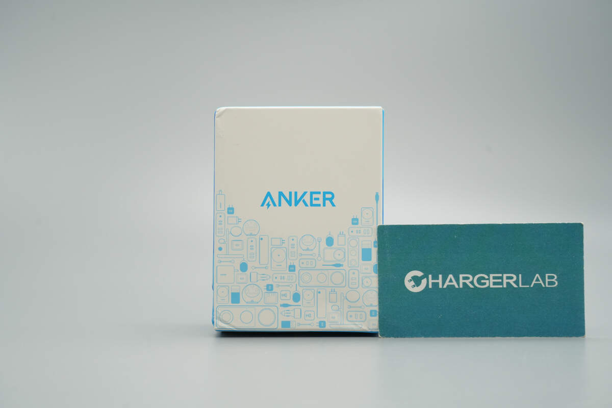
The front of the packaging features the ANKER logo.
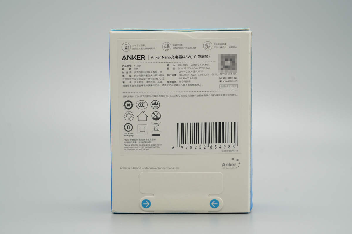
The back of the packaging has an information sticker.
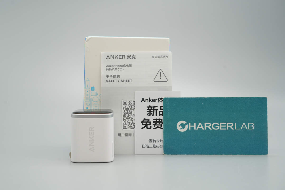
The package includes the charger, along with a user manual and other accessories.
The charger is wrapped in anti-scratch protective paper.
The outer casing is made of PC flame-retardant material.
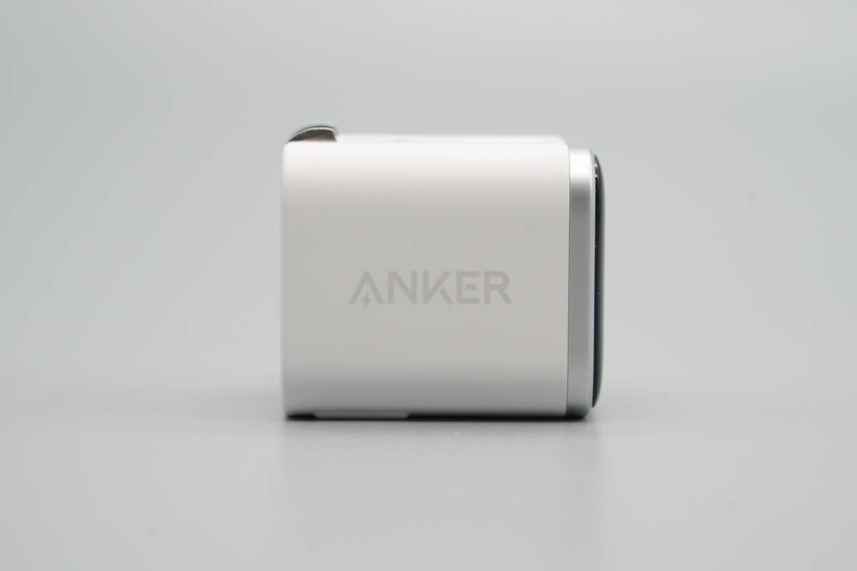
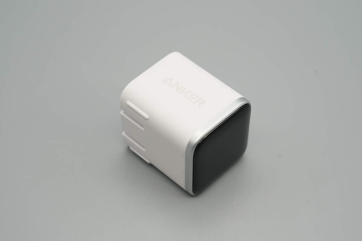
One side features the ANKER logo.

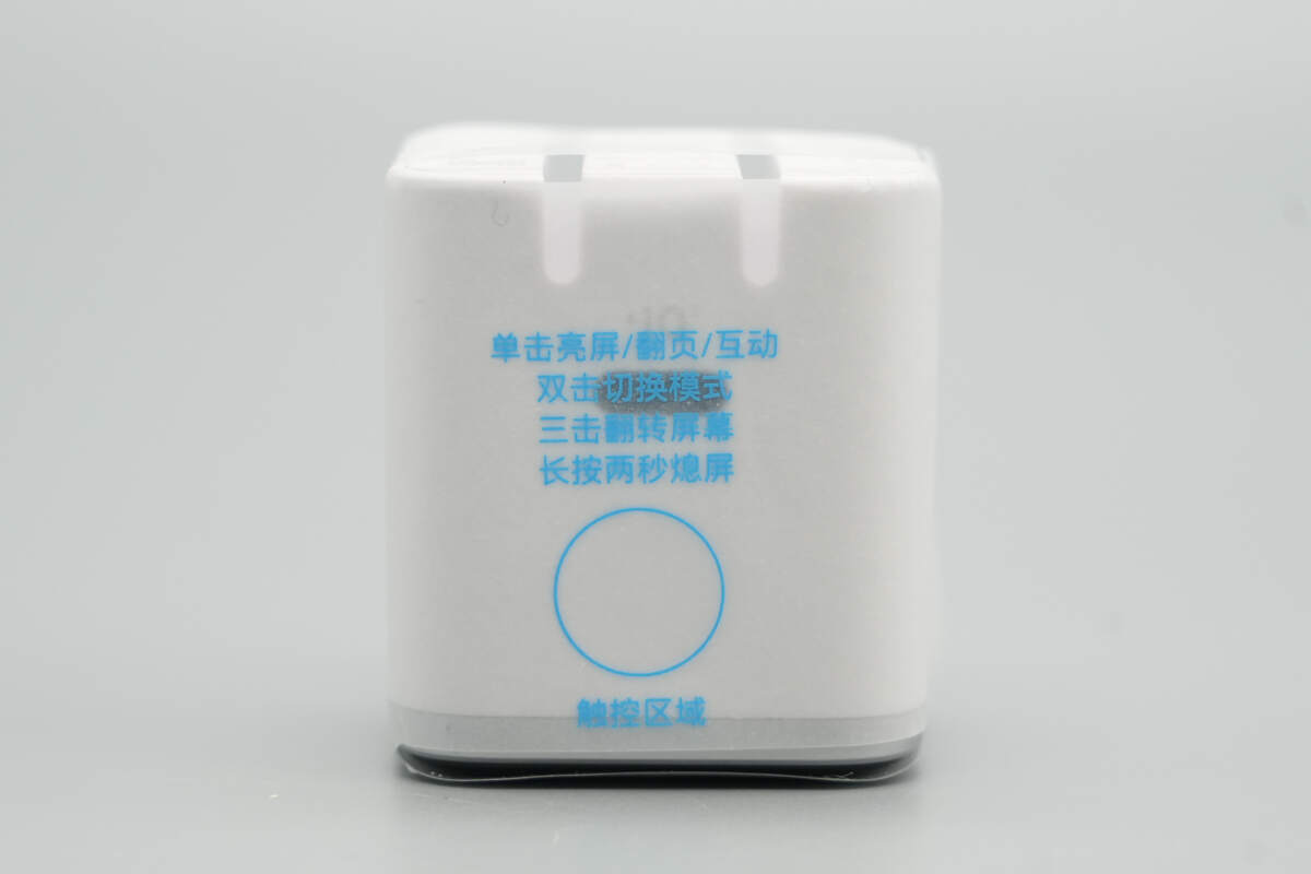
This side features a touch control button and a USB-C port, with a recessed design for the touch area.

The top black panel houses the smart interactive display.
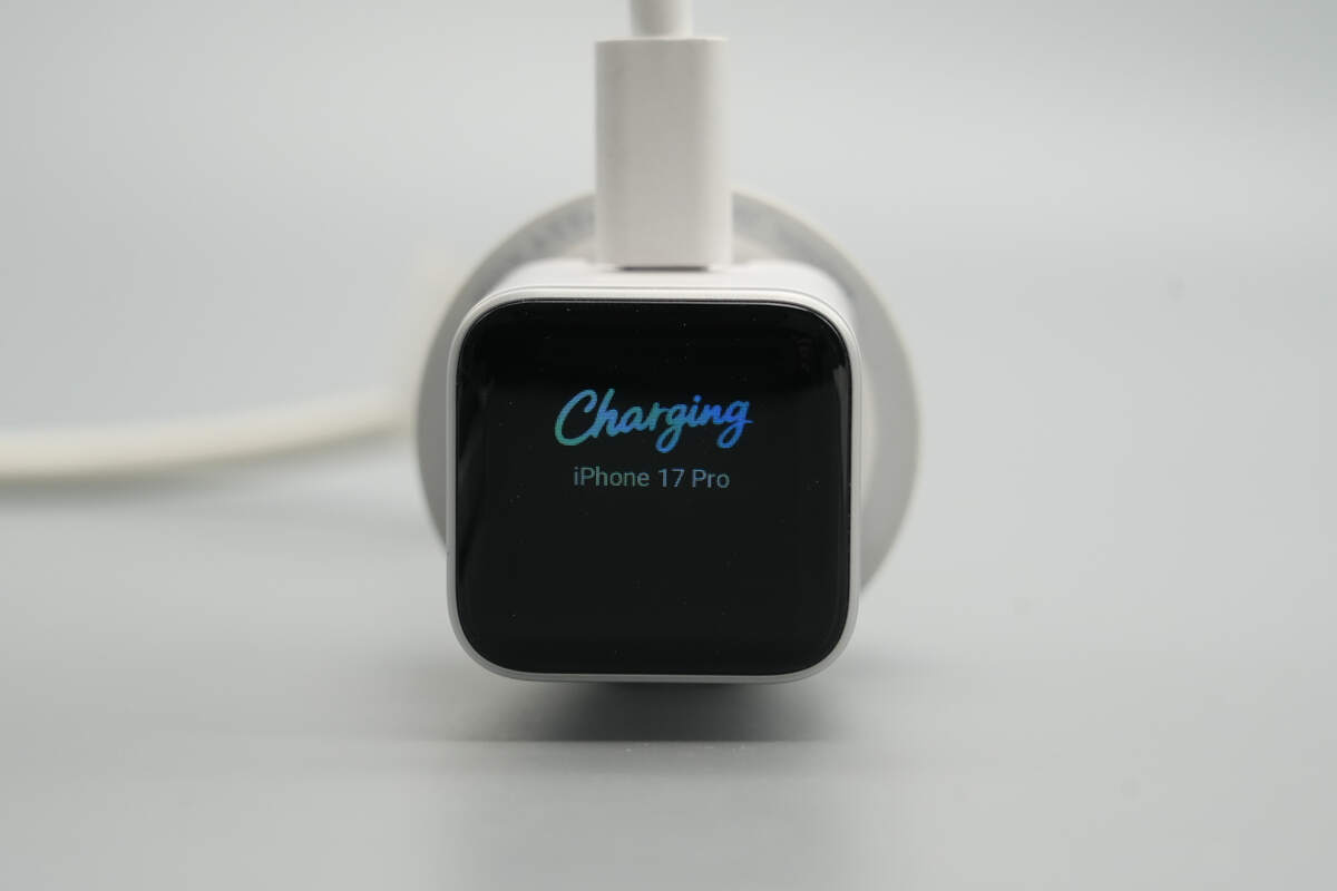
It supports recognition of the iPhone 17/16/15 series and USB-C iPads, and automatically adjusts the current/voltage accordingly.
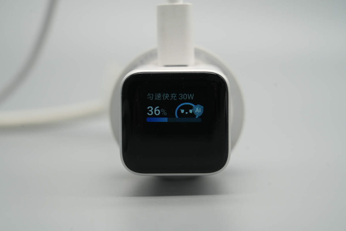
It can also display the charging status, power output, and progress.
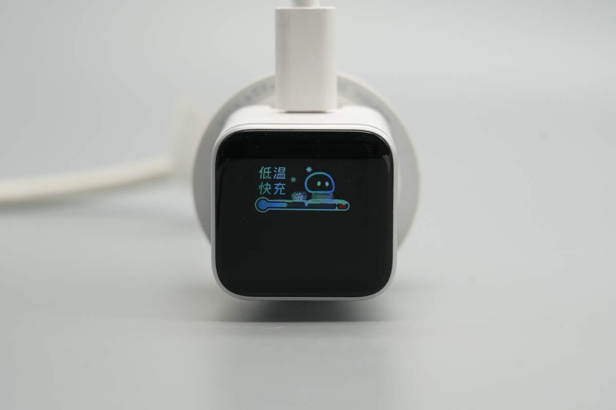
It can also indicate the current temperature status.
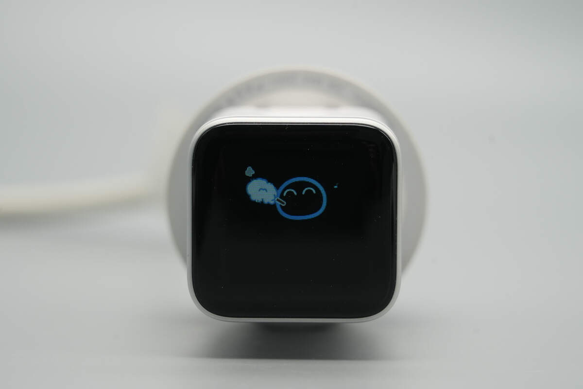
It also features a variety of fun emojis.
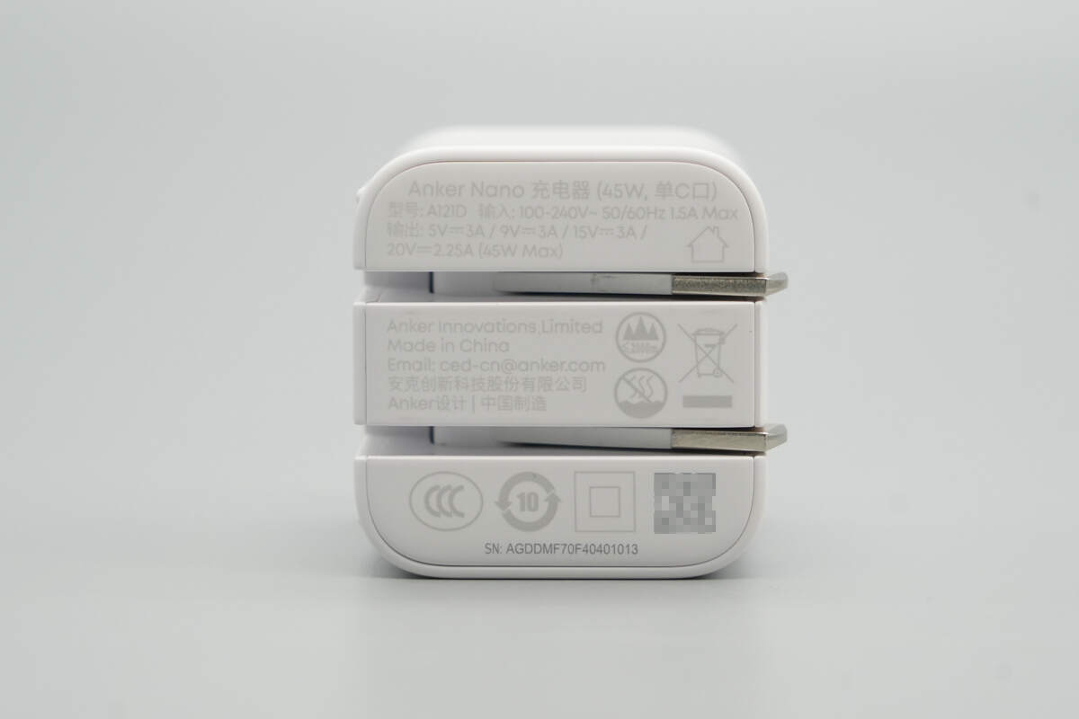
The input side of the casing is printed with the specifications.

Model: A121D
Input: 100-240V~50/60Hz 1.5A Max
Output: 5V 3A, 9V 3A, 15V 3A, 20V 2.25A (45W Max)
The charger has passed CCC certification.
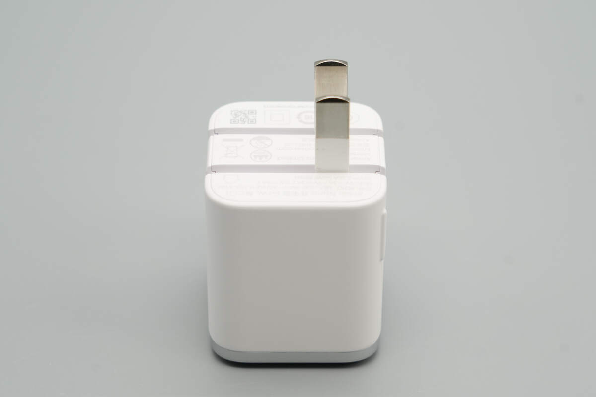
It comes with foldable prongs.
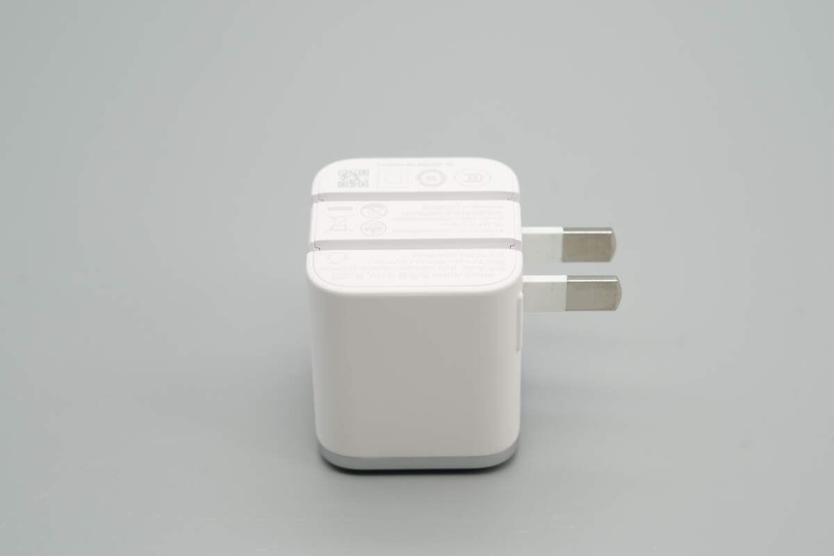
The prongs feature a patented 90° + 180° dual-fold design, allowing use in confined spaces without restriction.

The length of the charger is about 40.3 mm (1.59 inches).
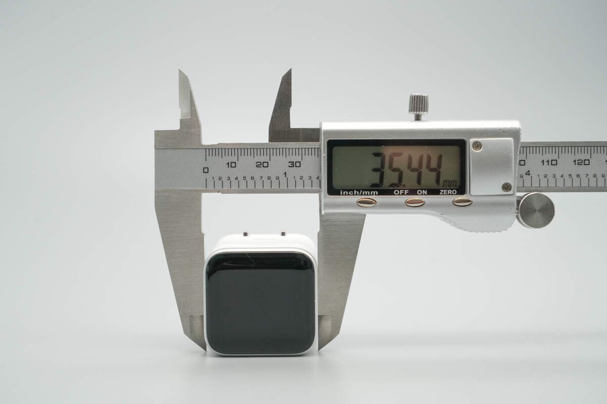
The width is about 35.44 mm (1.4 inches).
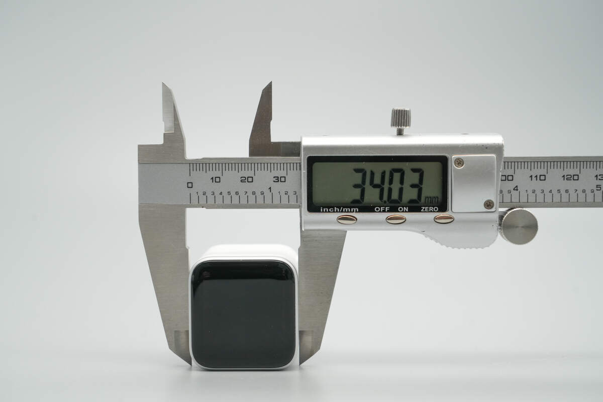
The thickness is about 34.03 mm (1.34 inches).
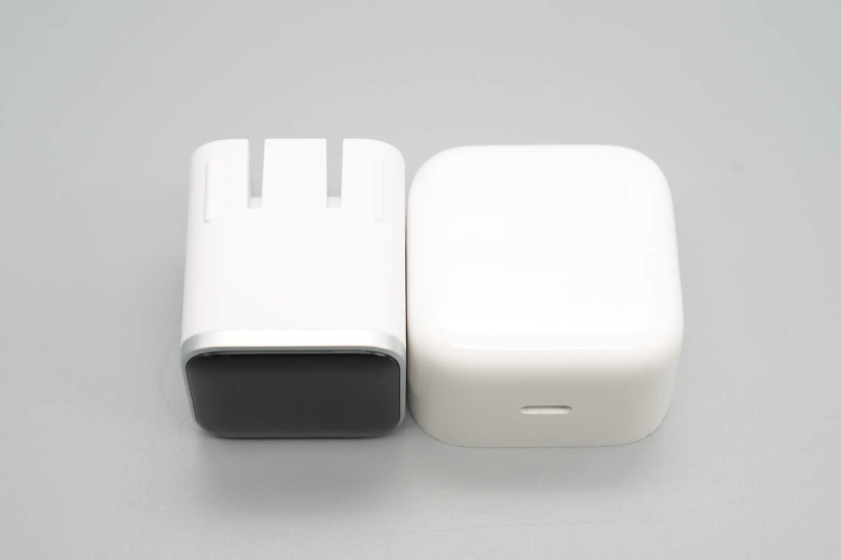
It is slightly smaller in size compared to Apple's 40W Dynamic Fast Charger.
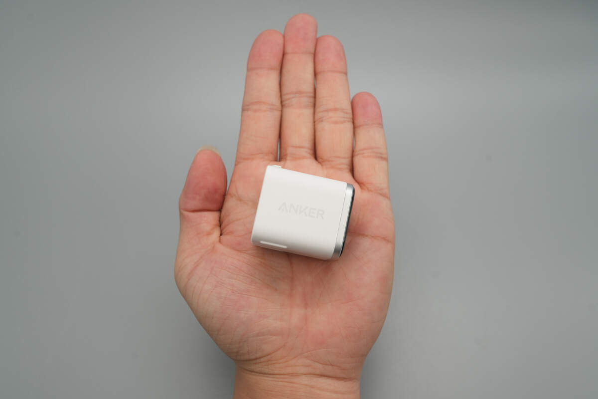
That's how big it is in the hand.
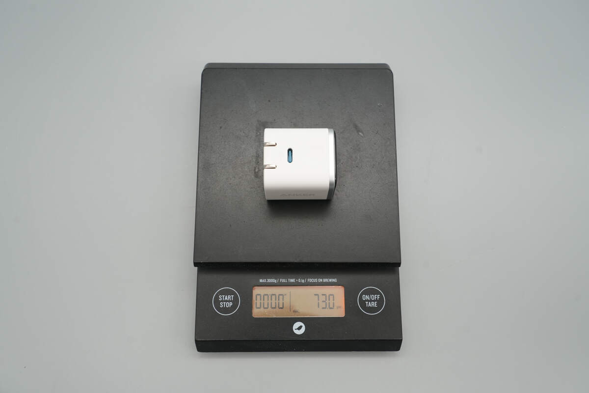
The weight is about 73 g (2.57 oz).

ChargerLAB POWER-Z KM003C shows that it supports QC3.0/4+, FCP, SCP, AFC, PD3.0, PPS, DCP, and Apple 2.4A protocols.
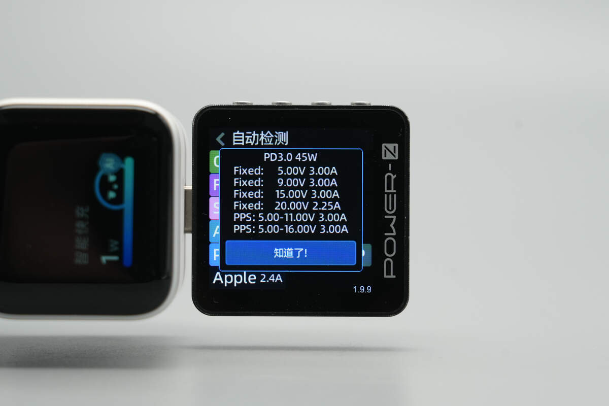
It has four fixed PDOs of 5V3A, 9V3A, 15V3A, and 20V2.25A. It also has two sets of PPS, which are 5-11V3A and 5-16V3A.
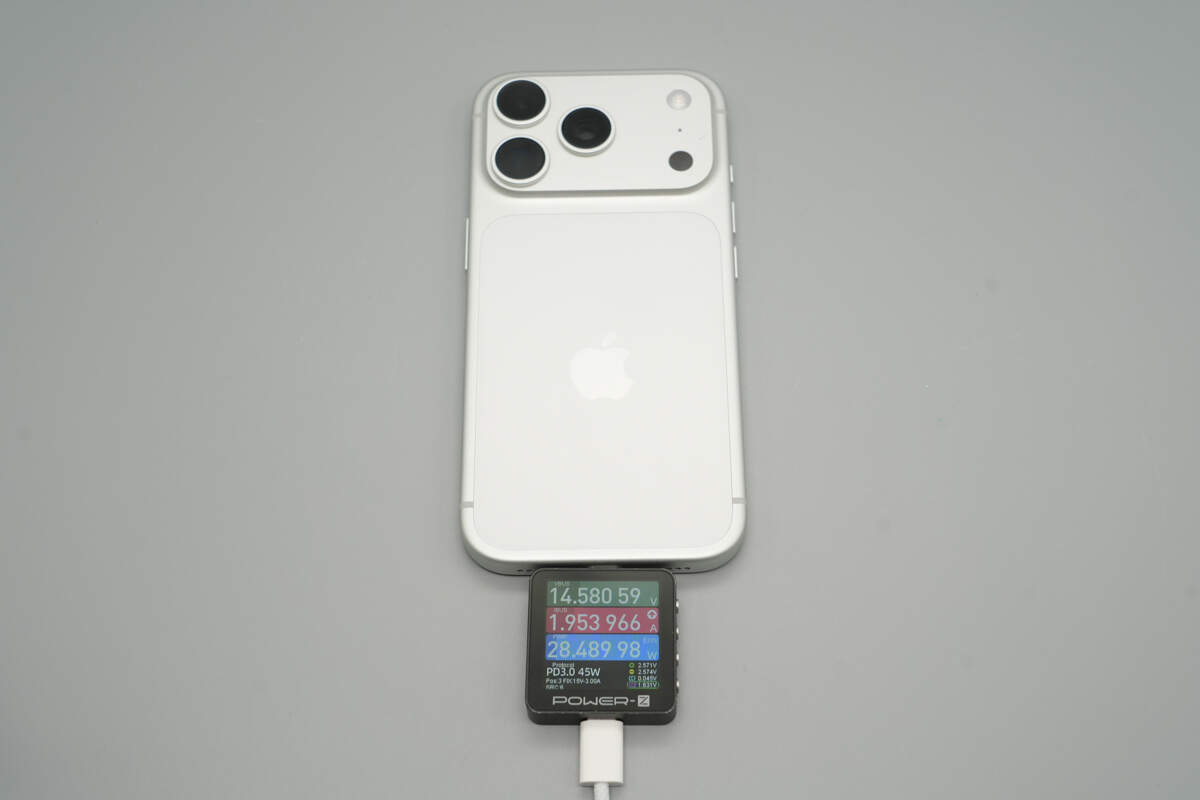
Use it to charge the Apple iPhone 17 Pro; the charging power is about 28.49W.
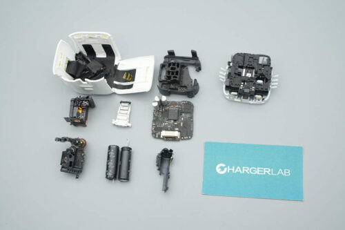
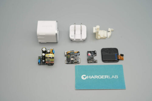
Teardown
Next, let's take it apart to see its internal components and structure.
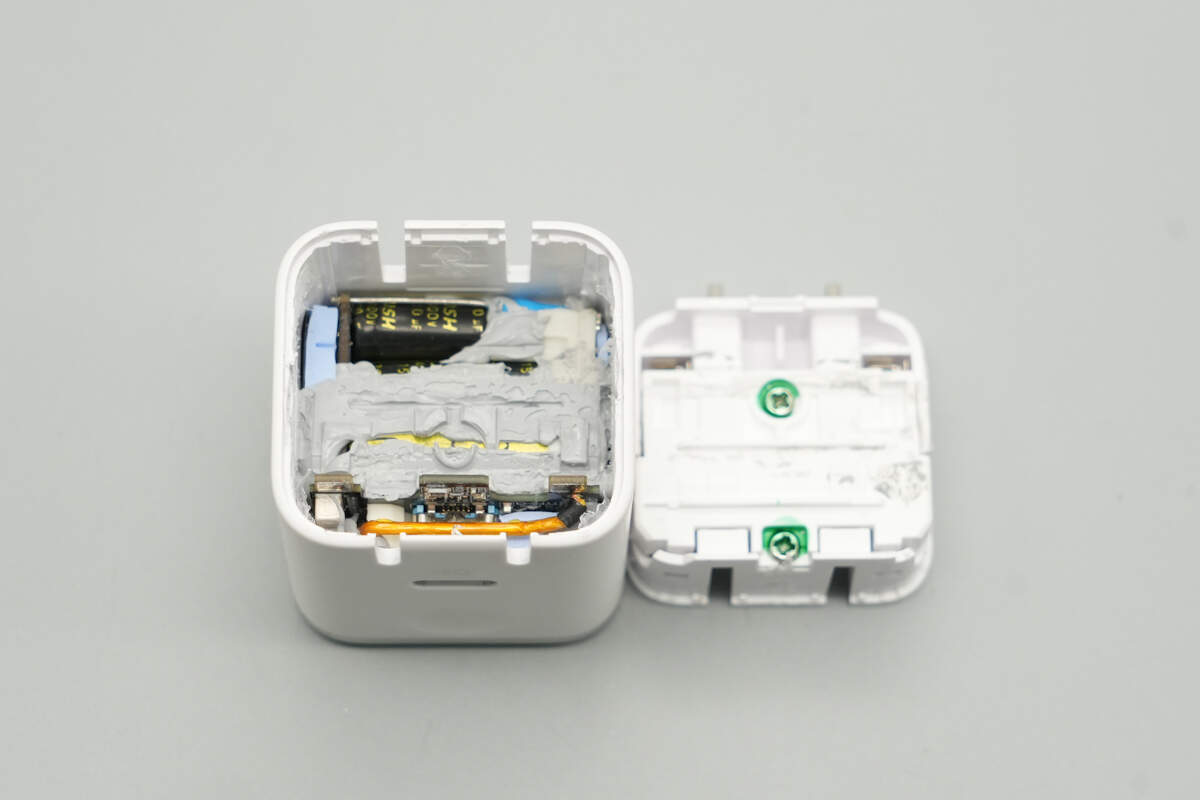
Remove the input-side casing. The prongs and the PCBA module use a contact-based power connection, with the prongs secured by a plastic cover and screws.
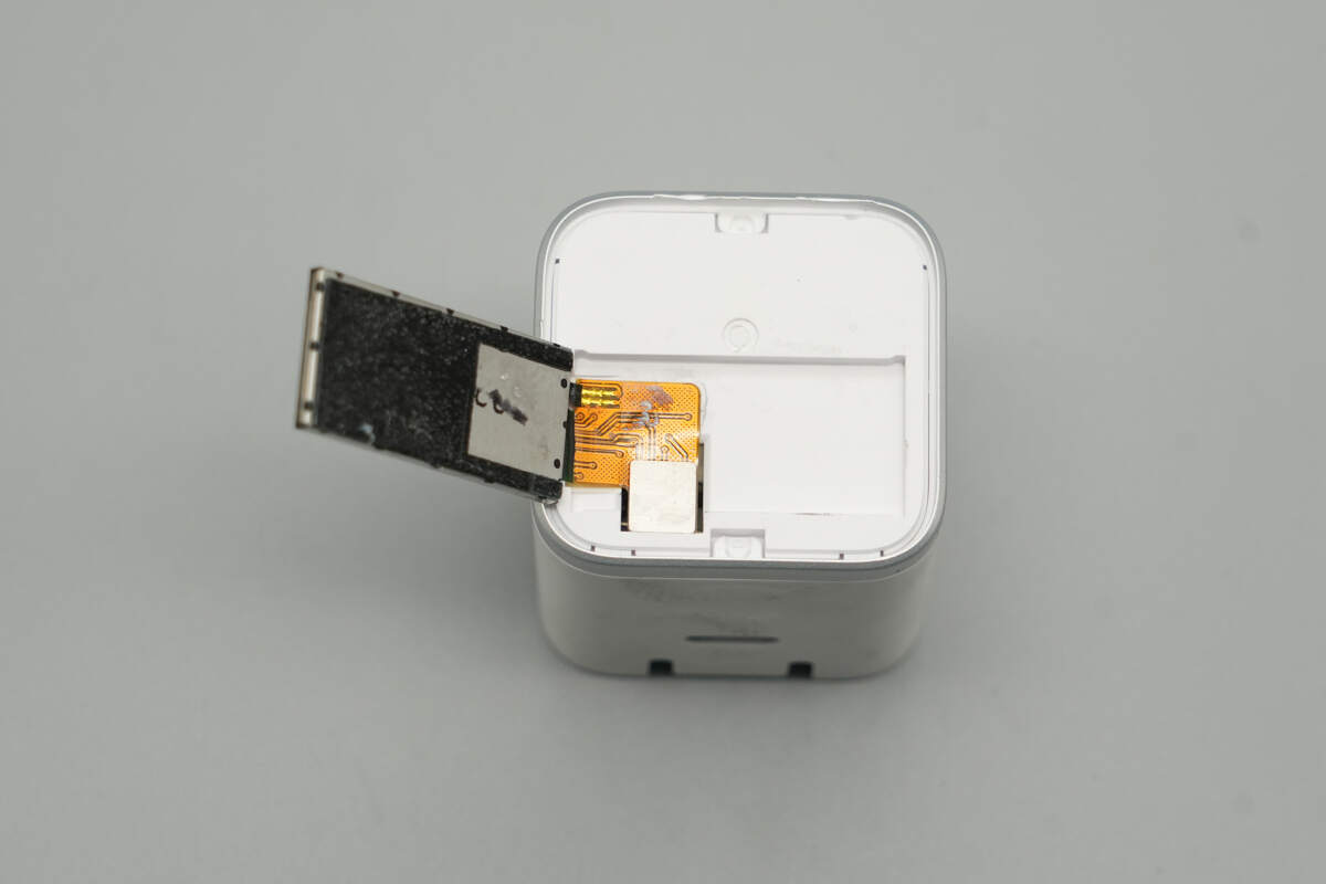
After removing the top black panel, it was found that the display is connected to the PCBA module via a flexible ribbon cable.
Remove the PCBA module.
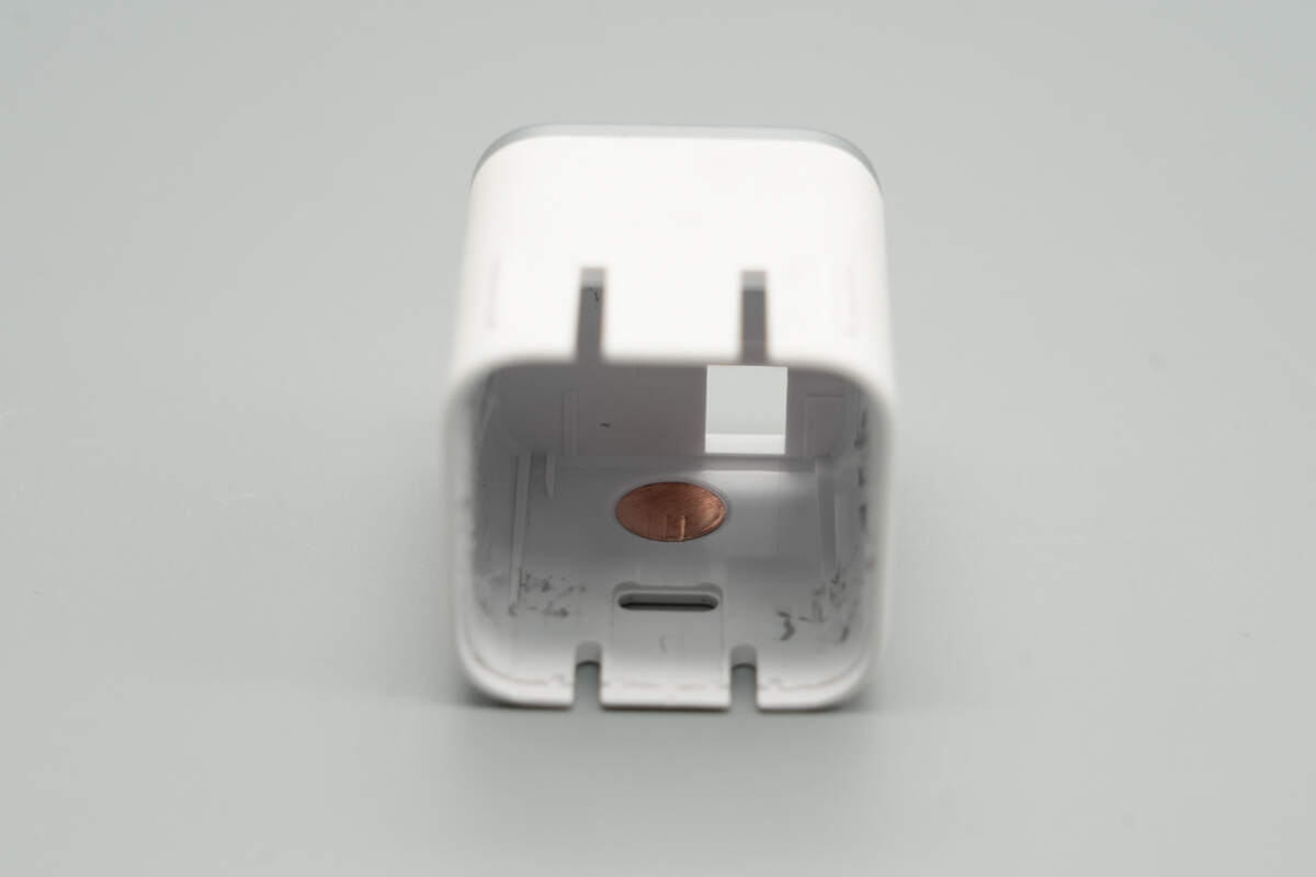
The inner side of the casing has a copper foil applied in the area corresponding to the touch button.
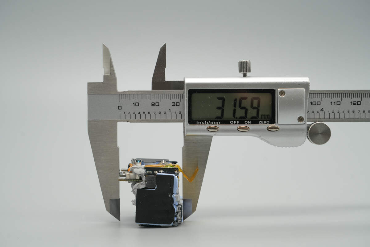
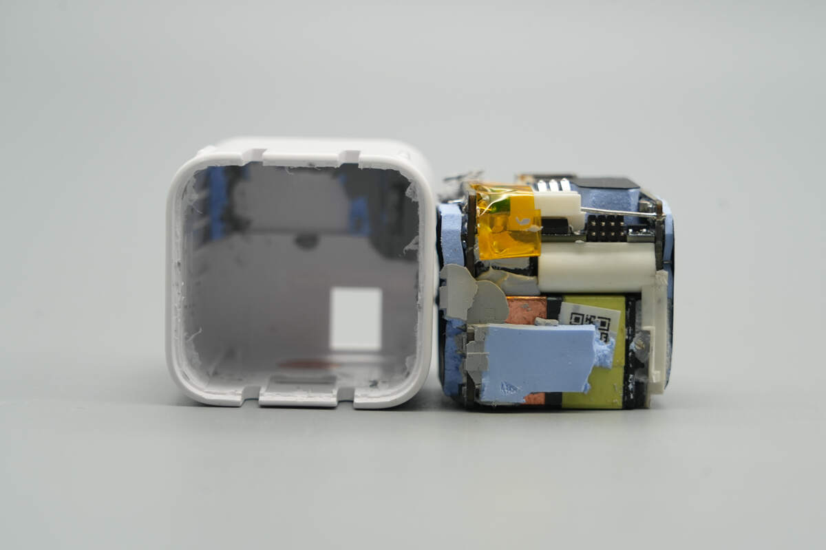
The length of the PCBA module is about 31.59 mm (1.24 inches).
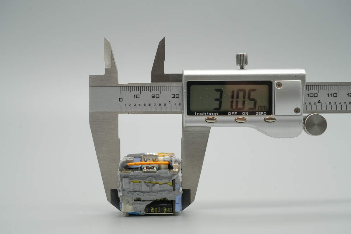
The width is about 31.05 mm (1.22 inches).
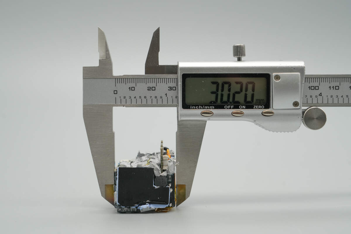
The thickness is about 30.2 mm (1.19 inches).
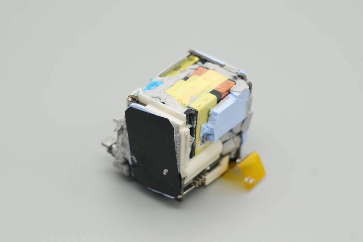
Thermal gel is applied between components.
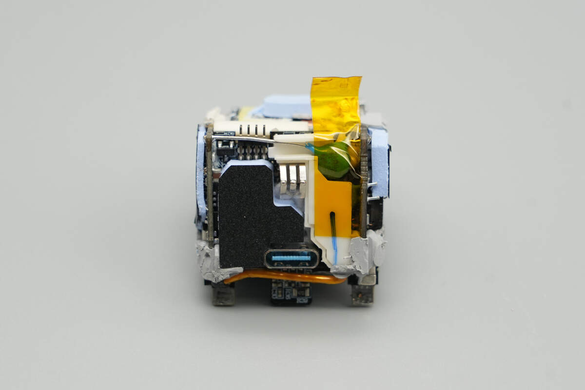
The front side of the output PCB is covered with a thermal pad, and the right-side area is reinforced with high-temperature insulating tape.

A plastic bracket is installed between the primary and secondary sections for isolation, while also providing structural reinforcement.
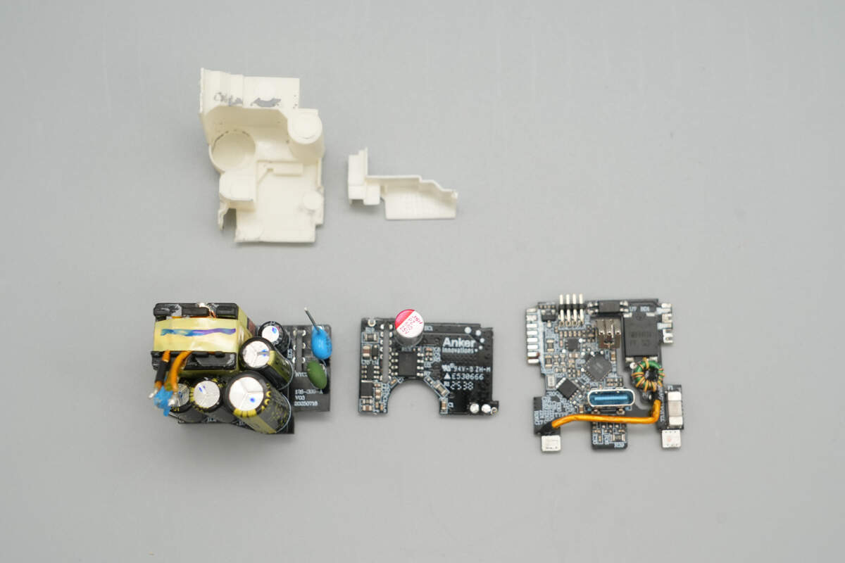
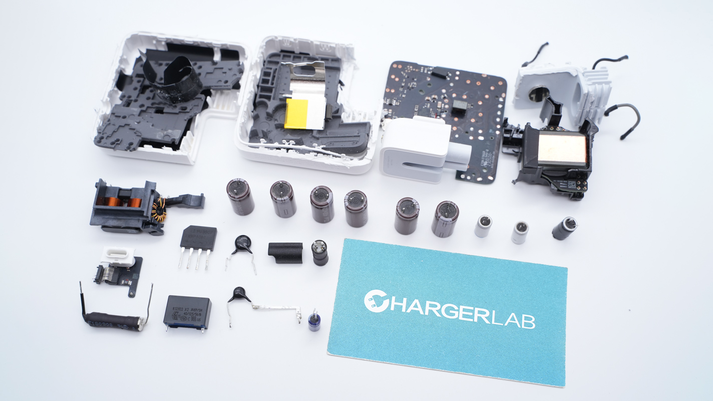
The PCBA module is disassembled into three separate PCBs.
The first PCB uses a cutout to separate the primary and secondary sides. Its front side houses components such as an SMD fuse, common mode choke, bridge rectifier, optocoupler, protocol chip, and output VBUS MOSFET.
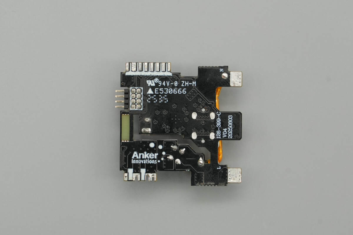
The back side has no components.

The front side of the second PCB houses an NTC thermistor, high-voltage electrolytic capacitors, a capacitor supplying power to the master control chip, a transformer, and Y capacitors.
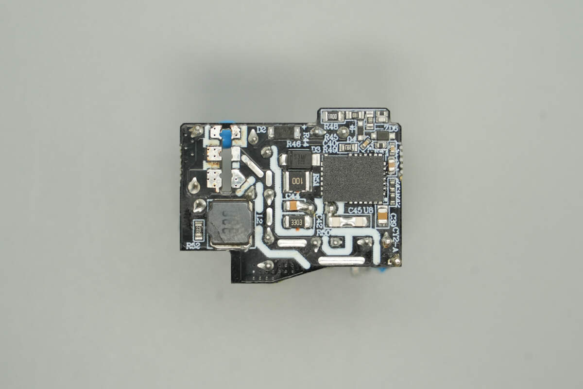
The back side features an I-shaped inductor and a packaged GaN chip.
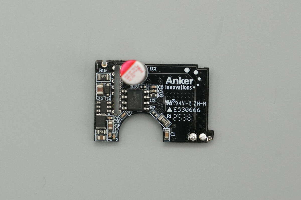
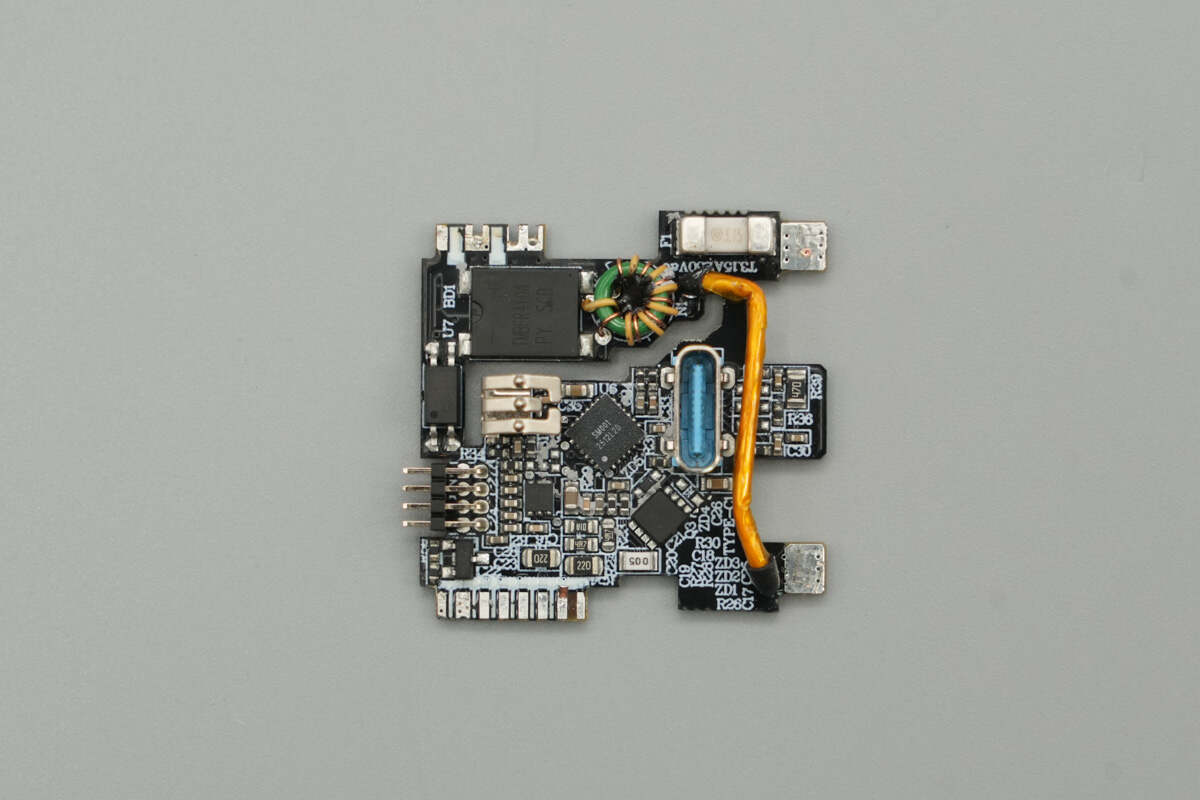
The front side of the third small PCB houses a solid capacitor for output filtering, a synchronous buck converter, memory, and other components.
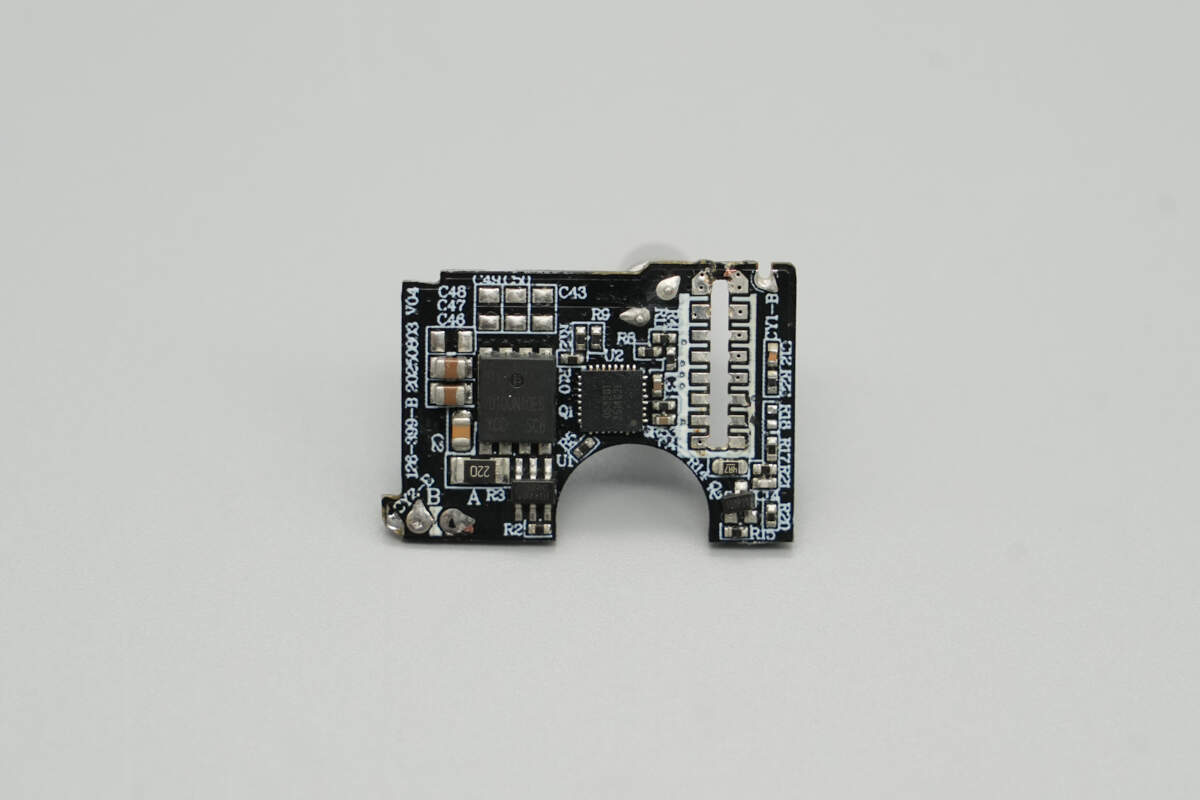
The back side features a synchronous rectifier controller, a synchronous rectifier, and an MCU.
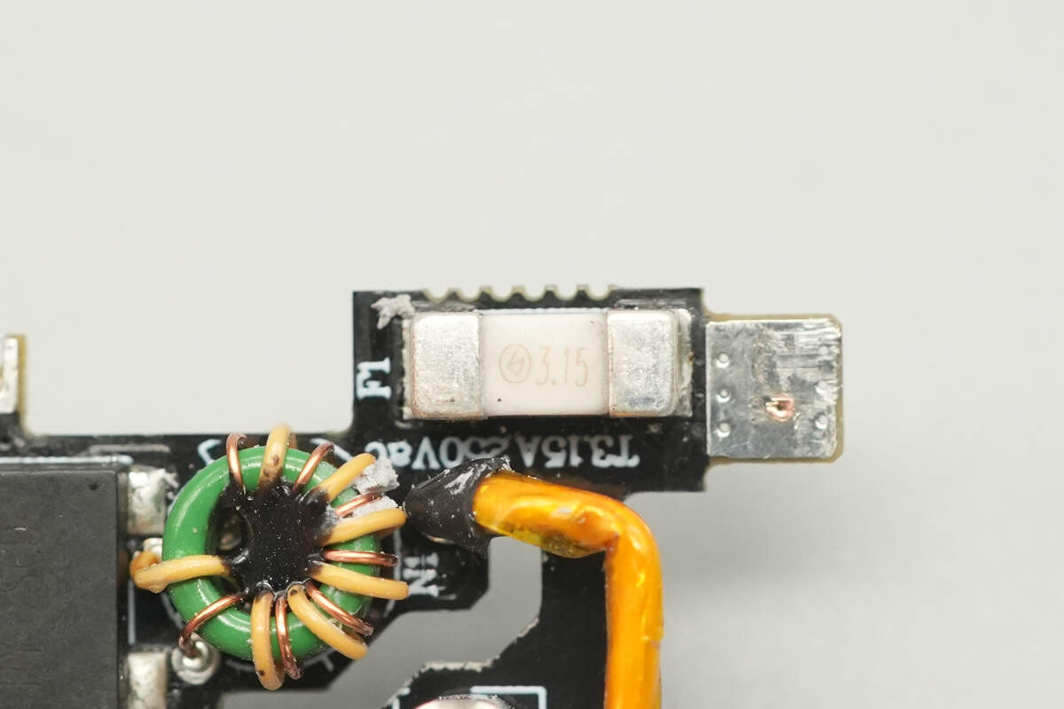
The SMD fuse is from Betterfuse, rated at 3.15A.
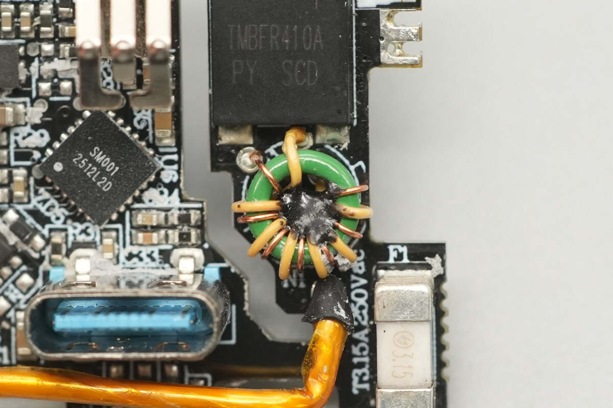
The common mode choke is a dual-wire winding, used to suppress EMI interference.
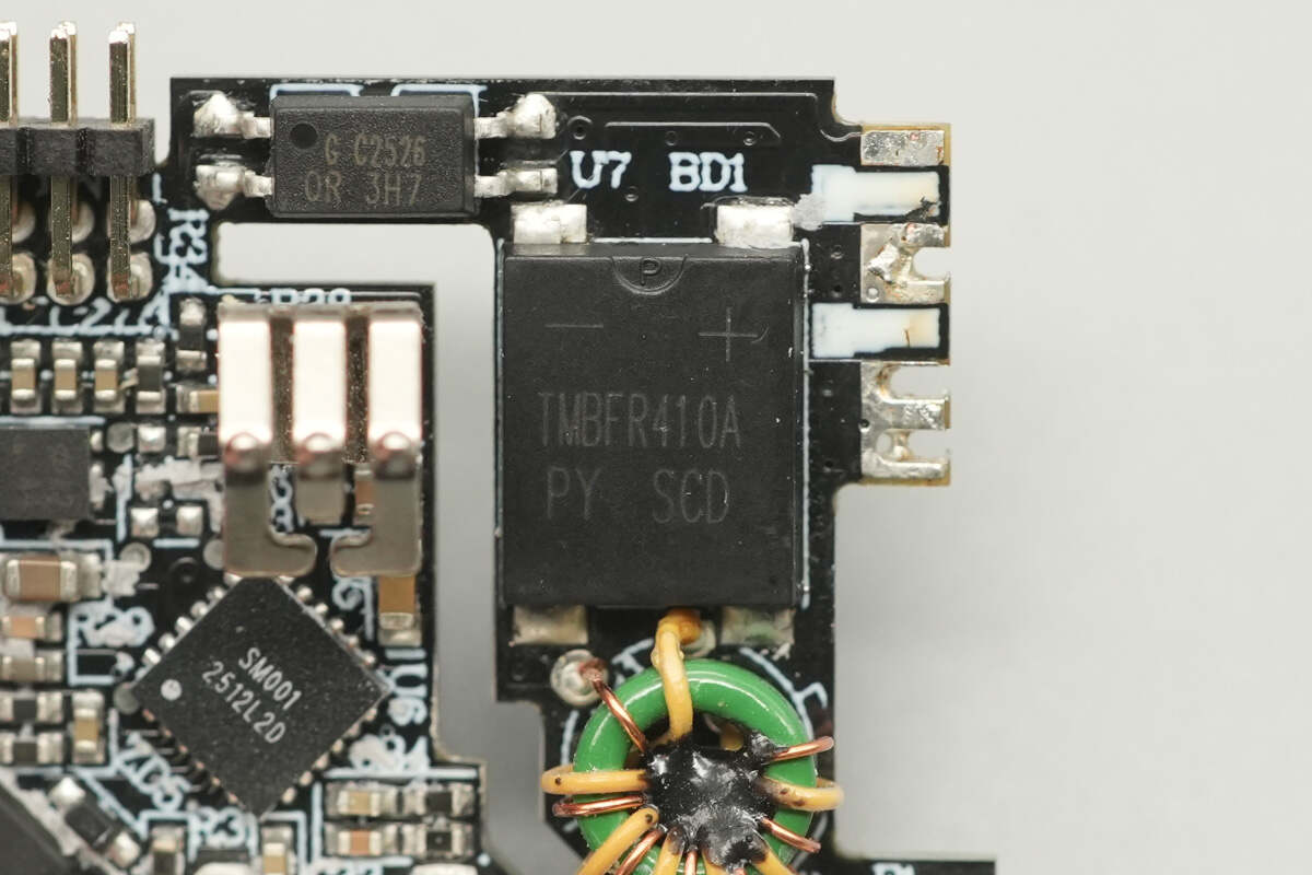
The bridge rectifier is from Pingwei, model TMBFR410A, rated at 1000V 4A, and uses a TMBF package.
The NTC thermistor is used to suppress inrush current during power-on.
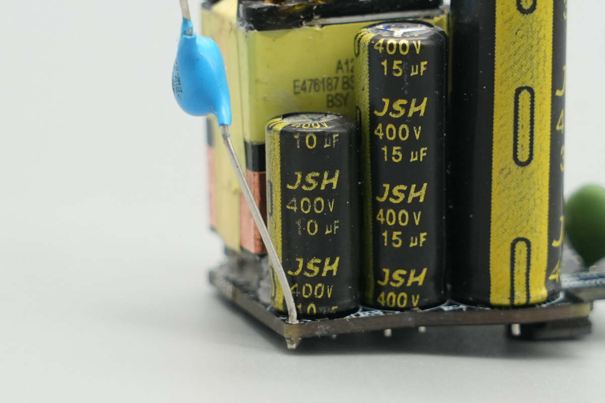
The primary side has four high-voltage filter electrolytic capacitors, all from JSH, with two of them rated at 400V 10μF and 400V 15μF, respectively.
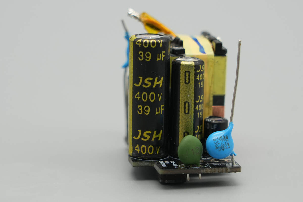
The third capacitor is rated at 400V 39μF.

The fourth capacitor is rated at 400V 15μF.
Close-up of the I-shaped inductor.
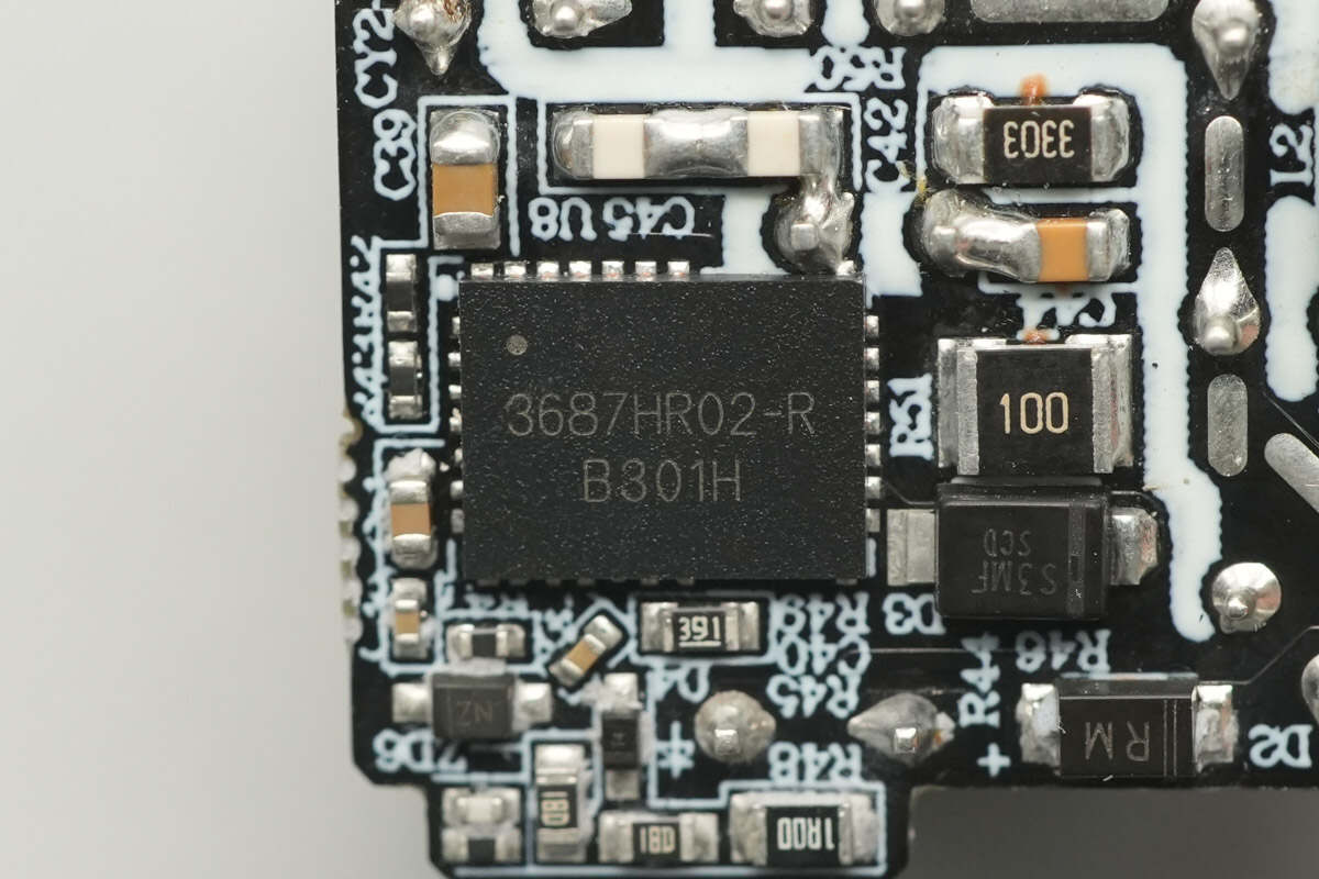
The integrated GaN chip is from HYASiC, model HYC3687HR02-R. The HYC3687H series is an all-in-one controller combining PWM, sense FET, and GaN. This controller features lossless current sensing, integrated high-voltage startup, and eliminates the need for conventional sense resistors, further improving efficiency, reducing external components, and lowering system cost.
The chip internally integrates a 700V DGaN, tailored for market demands and highly suitable for compact power supplies. Its patented D-GaN drive technology and adjustable switching speed enhance EMI performance. Packaged in a DFN 6mm × 8mm, it balances cost and thermal management effectively. Paired with a Huayuan synchronous rectifier chip, it ensures reliable system operation in CCM, QR, or DCM modes.

The HYC3687H/X integrates comprehensive protection features, including output overvoltage protection, transformer saturation protection (TSP), chip supply overvoltage protection, overload protection (OLP), over-temperature protection (OTP), undervoltage protection, and on-chip over-temperature protection. It comes in a QFN 6×8mm package.

The capacitor supplying power to the master control chip is also from JSH, rated at 63V 10μF.
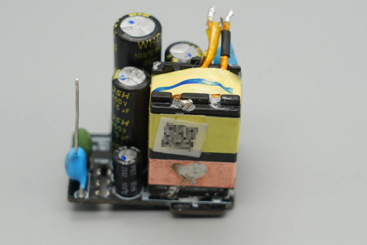
Close-up of the transformer.
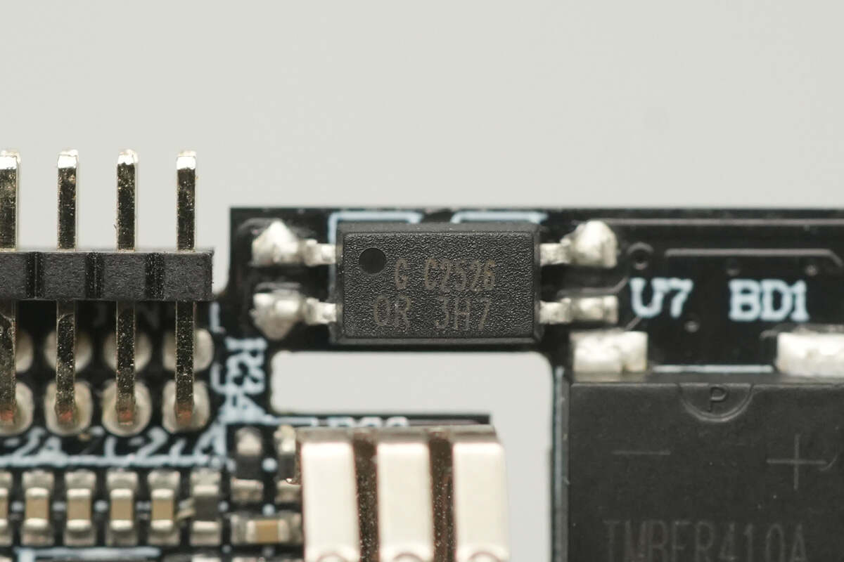
The OR 3H7 optocoupler is used for output voltage feedback.
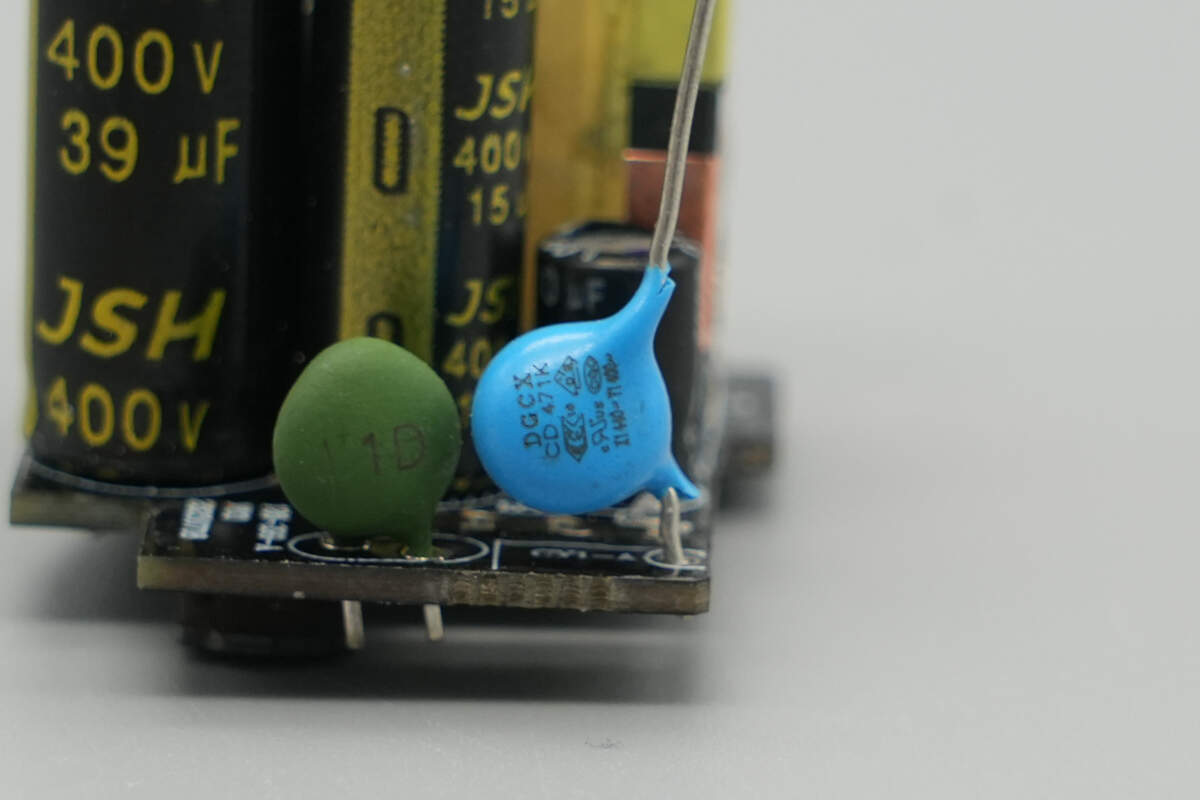
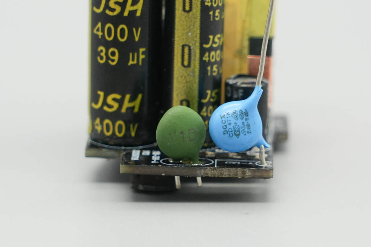
The blue Y capacitor is from DGCX.
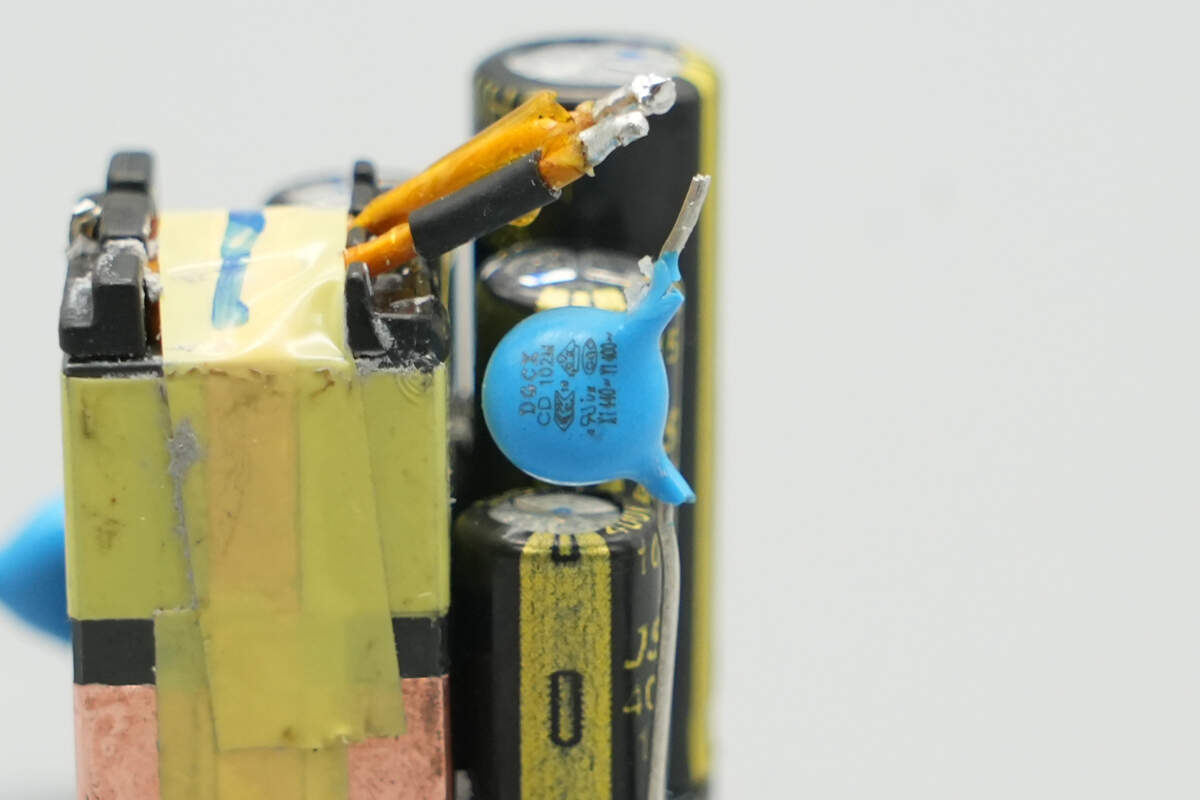
The other blue Y capacitor is also from DGCX.
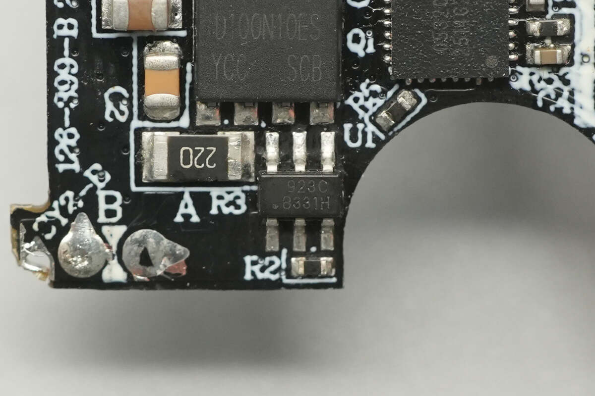
The synchronous rectifier controller is from HYASiC, model HY923. It is a digital adaptive synchronous rectifier controller that supports both high-side and low-side applications without requiring an auxiliary winding for power. The chip supports DCM, CCM, PFM, and QR operating modes, with a supply voltage range of 3.2–25V and a withstand voltage of 150V.
HY923 features high-current drive capability suitable for various synchronous rectifiers, with a gate drive voltage clamped at 7V and an active pull-down function at startup, compatible with MOSFETs from different manufacturers. It provides direct-through protection, optimizes switching losses and EMI, and has low quiescent current. The chip comes in an SOT23-6 package.
Here is the information about HYASiC HY923.

The synchronous rectifier is from Pingwei, model D100N10ES, an N-channel MOSFET with a voltage rating of 100V and an on-resistance of 5mΩ, packaged in DFN 5×6mm.

The solid capacitor for output filtering is from JSH, rated at 25V 560μF.
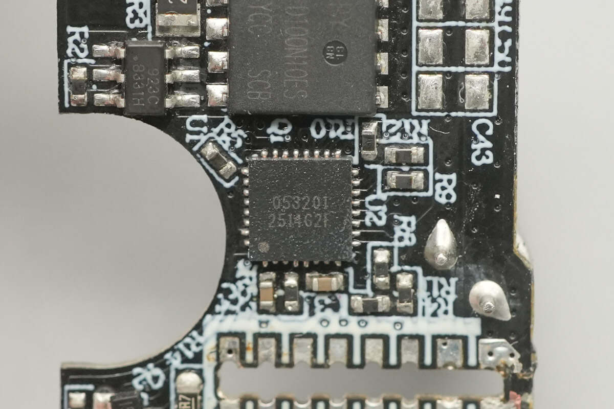
The MCU used for display control is marked 05320T and comes in a QFN32 package.
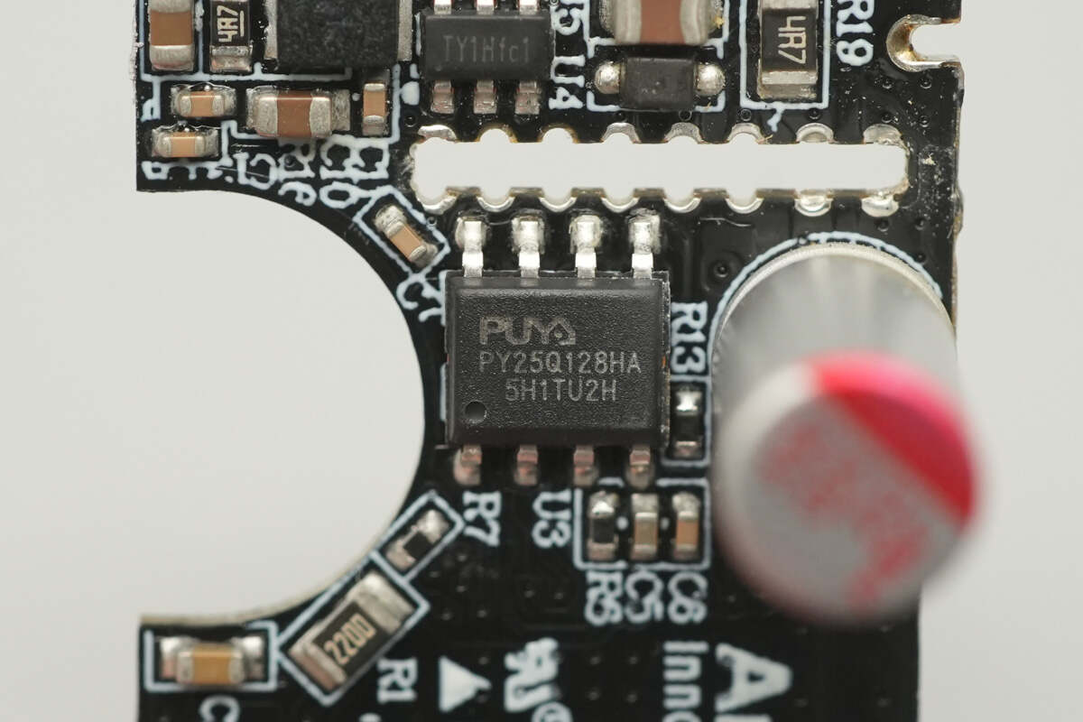
The memory is from Puya, model PY25Q128HA, in an SOP8 package, used for storing configuration data.
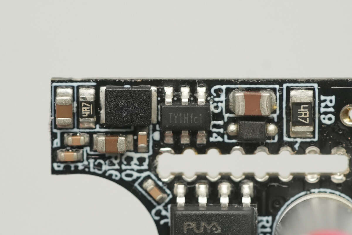
The synchronous buck converter used to step down the voltage for the MCU and display is from TOLL, marked TY1H, model TMI3341. It is a high-efficiency 1.5MHz synchronous buck converter capable of delivering up to 1.2A output current.
The TMI3341 integrates high- and low-side MOSFETs, with low on-resistance to effectively reduce conduction losses. Under light-load conditions, the chip operates in pulse frequency modulation (PFM) mode, significantly improving light-load efficiency. Its 1.5MHz switching frequency achieves low output voltage ripple while allowing the use of compact inductors and capacitors, requiring only a few standard external components. The chip comes in a RoHS-compliant 6-pin SOT23-6 package.
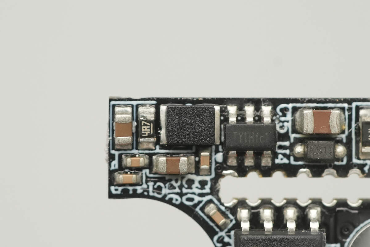
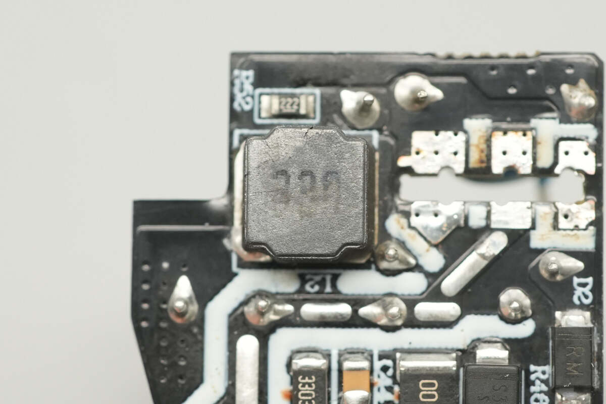
Next to it is an SMD buck inductor.

The protocol chip is marked SM001 and comes in a QFN24 package.

The USB-C port output VBUS MOSFET is from Allpower, model AP30H80Q, an N-channel MOSFET with a voltage rating of 30V and an on-resistance of 4.1mΩ, packaged in PDFN 3×3mm.
The back of the display is lined with foam padding.
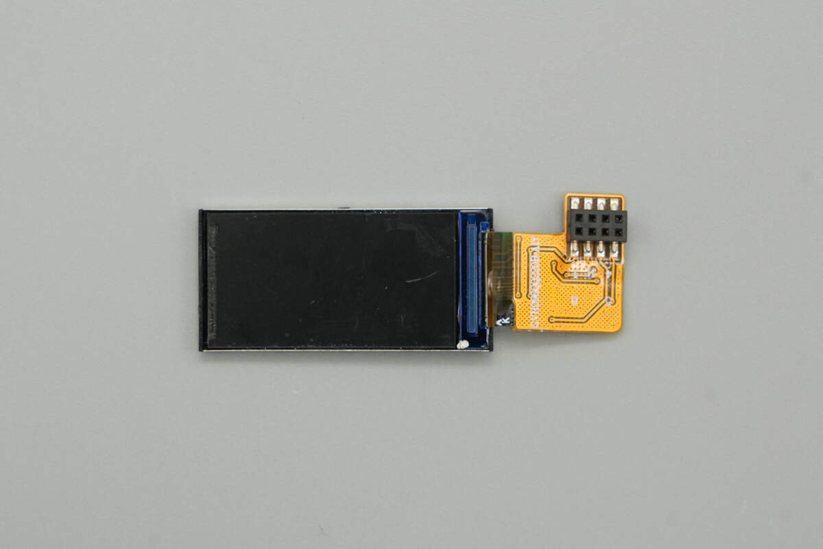
The ribbon cable features a pin header socket.

Well, those are all components of the Anker Nano 45W GaN Charger with Display.
Summary of ChargerLAB
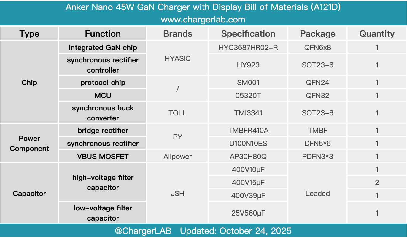
Here is the component list of the Anker Nano 45W GaN Charger with Display for your convenience.
The charger has a compact body. Its display supports rich real-time information, including charging power, temperature, device battery level, and fun emojis. It features an innovative 90° + 180° dual-fold prong design and can quickly recognize devices such as the iPhone 17, providing up to 45W fast charging.
After taking it apart, we found that it uses a three-PCB stacked design and employs a highly integrated GaN power solution with the HYASiC HYC3687HR02-R and HY923. This not only helps achieve a compact form factor but also ensures system reliability and efficiency. Thermal gel is applied between components on the PCBA module, and each small PCB is covered with thermal pads, providing effective heat dissipation.
Related Articles:
1. Teardown of Segotep 3200W Titanium-Rated SiC Digital Server Power Supply (CRPS3200W-12V)
2. Teardown of Xiaomi 33W Nano Power Adapter (MDY-19-ED)
3. Teardown of UGREEN 22.5W 20000mAh Power Bank with Built-in Cable (PB505)