Introduction
EcoFlow has launched a RAPID GaN Charger (65W, 3-port output), featuring a sleek and minimalist design that is compact and portable, making it easy to integrate into various environments. It is equipped with two USB-C ports and one USB-A port, supporting multiple fast charging protocols. The charger can deliver up to 65W per port, with intelligent power distribution, meeting the fast charging needs of laptops, smartphones, tablets, and other devices.
Recently, during a teardown of this EcoFlow charger, it was discovered that the primary side uses a high-voltage GaN MOSFET, the INN700D240B from Innoscience, in combination with the primary control chip. The following will provide a detailed introduction to this component.
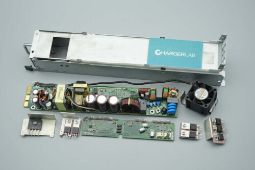
EcoFlow RAPID 65W GaN Charger
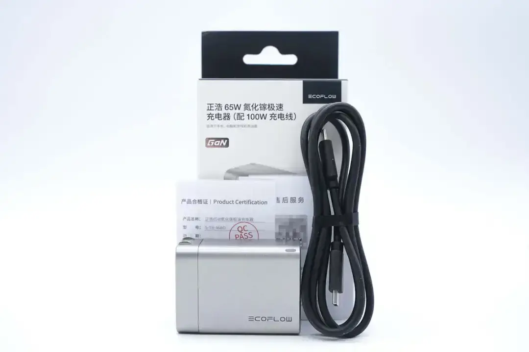
The box contains the EcoFlow RAPID 65W GaN charger, a dual USB-C cable, and some documents.
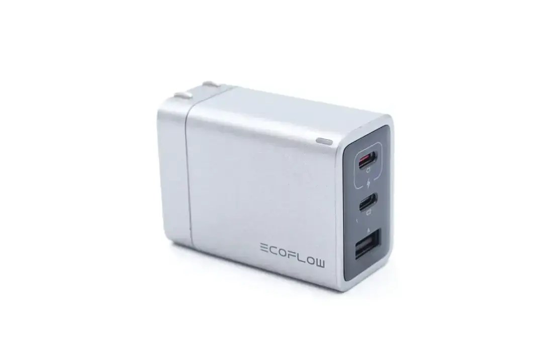
The shell is made of fire-retardant PC, and the surface is sprayed with silver-gray metallic paint, the overall appearance is quite fashionable.
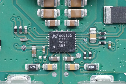
Innoscience INN700D240B
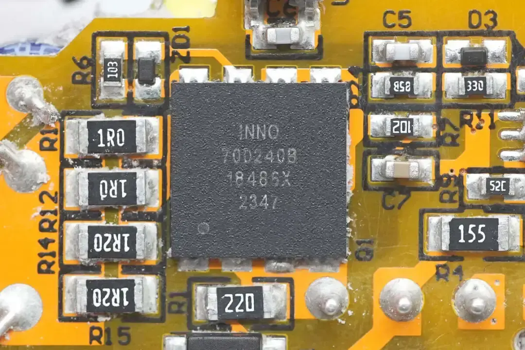
The primary MOSFET built into the EcoFlow charger uses the Innoscience INN700D240B, an enhanced GaN FET with a withstand voltage of 700V, a transient withstand voltage of 800V, and a conduction resistance of 240mΩ. It meets the JEDEC standard for industrial applications, has built-in ESD protection, and adopts a DFN8*8 package.
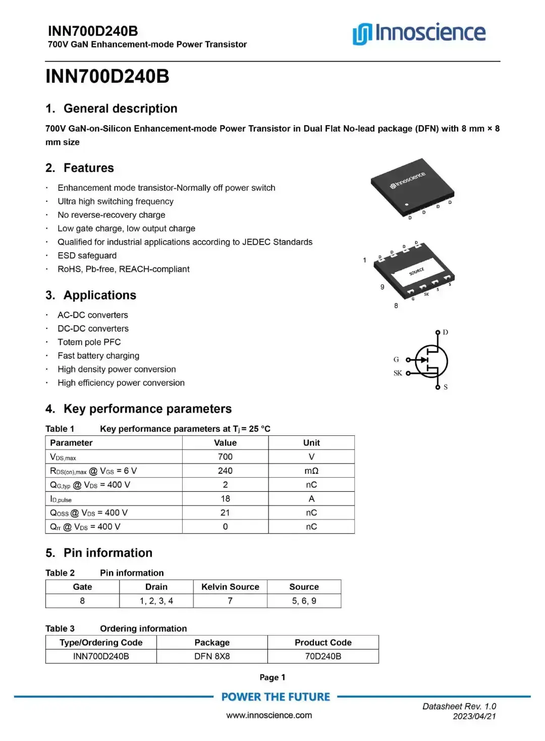
The component complies with JEDEC industrial application standards as well as RoHS and REACH regulations. It features zero reverse recovery charge, low gate charge, and low output charge, making it well-suited for applications such as PFC (Power Factor Correction), AC-DC and DC-DC conversion, and PD (Power Delivery) fast charging scenarios.
Summary of ChargerLAB
The Innoscience INN700D240B enhances the performance and reliability of the charger. With characteristics such as zero reverse recovery charge, low gate charge, and low output charge, it delivers excellent performance and plays a key role in helping EcoFlow provide users with a more efficient and convenient charging experience.
Innoscience is a global leader in third-generation semiconductor technology, specializing in the research and manufacturing of GaN-on-Si (gallium nitride on silicon). The company operates the world’s largest 8-inch GaN-on-Si wafer fabrication facility and offers product designs and performance that are at the forefront of the industry. Innoscience's GaN products cover a wide range of voltage applications—from 15V to 1200V—including wafers, discrete devices, ICs, and modules, delivering comprehensive GaN solutions for its clients. Since its founding, Innoscience has filed or been granted nearly 700 patents. Its products are widely used in cutting-edge fields such as consumer electronics, renewable energy, industrial applications, automotive electronics, and data centers.