Introduction
We obtained Xiaomi’s overseas 33W GaN charger, which features a compact cubic design measuring just 32 × 32 × 32 mm. According to preliminary information, this charger adopts a complete power solution from Injoinic. Below, we take a closer look at the internal components and design.
Product Appearance
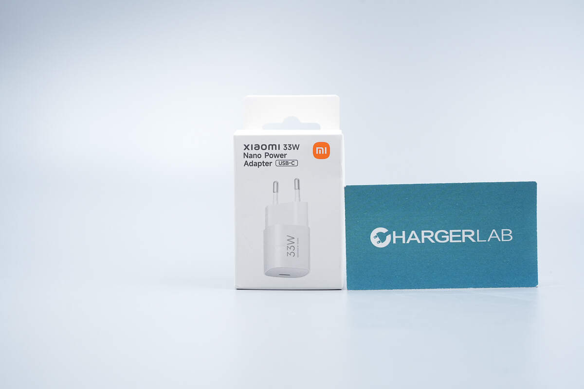
The front of the packaging box features the Xiaomi logo, the product name, and an image of the charger.

A specification label is affixed to the back of the box.

The package includes the charger, a user manual, and related documentation.
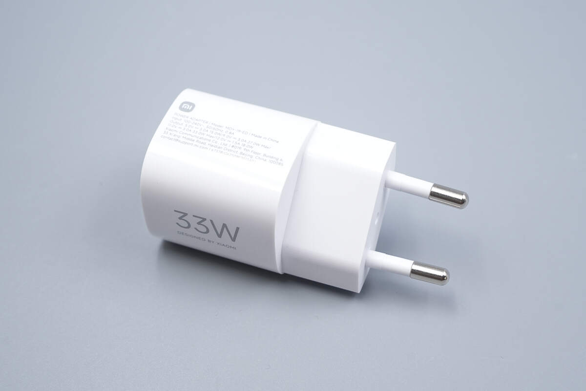
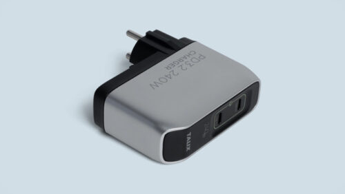
The outer casing is made of flame-retardant PC material with a glossy surface finish.
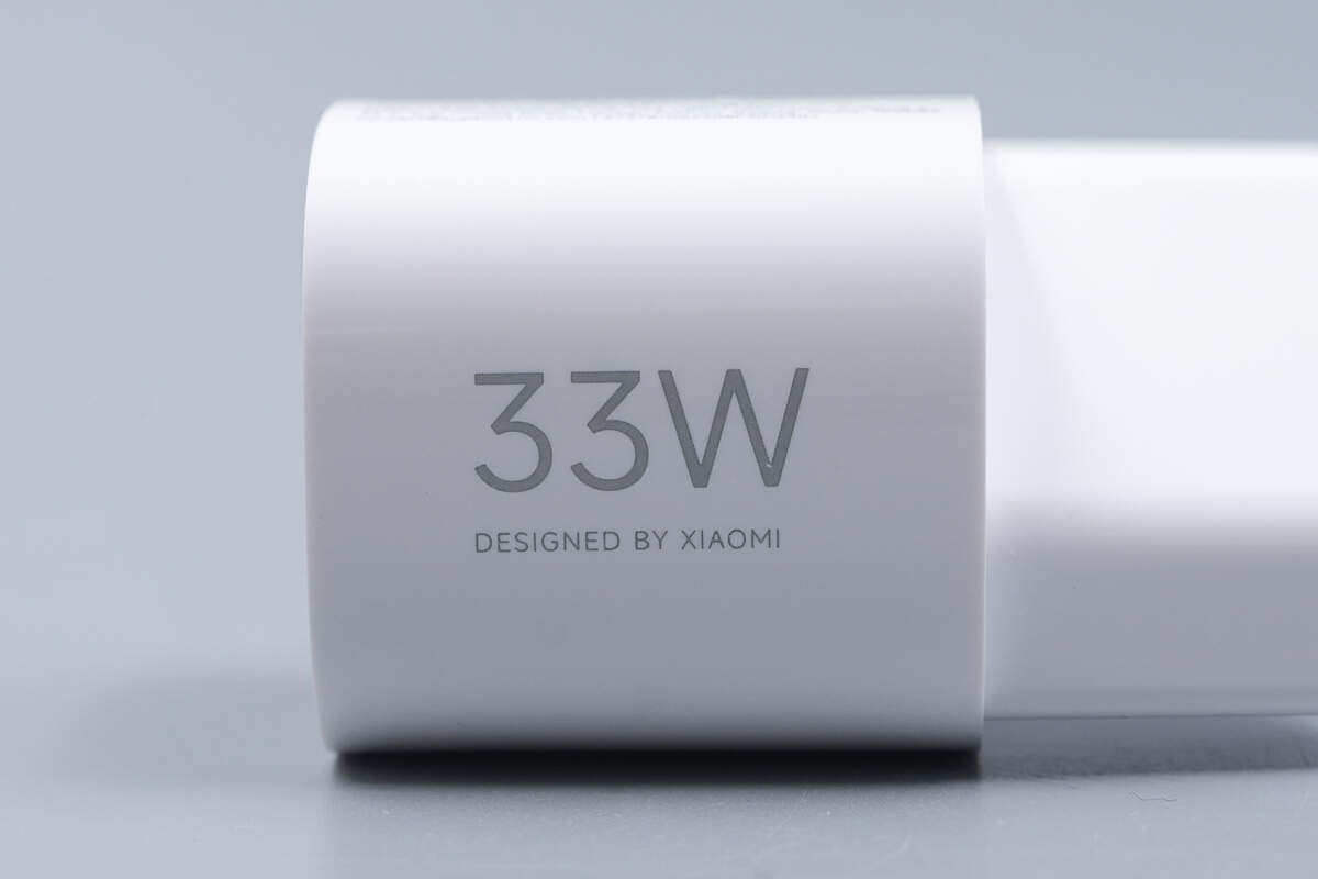
This side is printed with “33W” and “Designed by Xiaomi.”
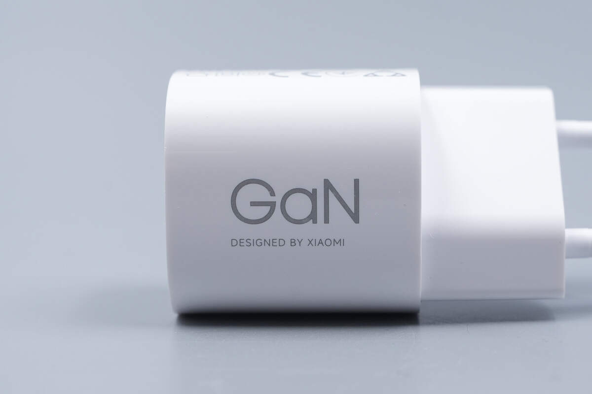
The opposite side is printed with “GaN” and “Designed by Xiaomi.”

The third side lists the product specifications:
Model: MDY-19-ED
Input: 100–240V~ 50/60Hz 0.8A
Output: 5V⎓3A, 9V⎓3A, 11V⎓3A Max, 12V⎓1.5A

It has passed CE, EAC, and CP certifications, as well as Level VI energy efficiency certification.
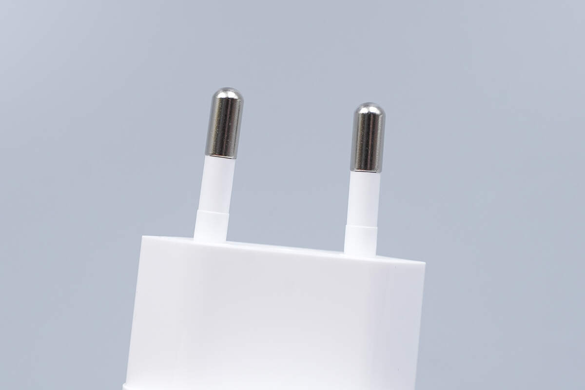
The plug features a European standard configuration.

The top surface features a USB-C output port.
The length of the charger is about 32.19 mm (1.27 inches).

The width is about 32.18 mm (1.27 inches).

The thickness is about 32.1 mm (1.26 inches).

Its size is close to that of Apple’s 5W charger, making it extremely compact.

That's how big it is in the hand.
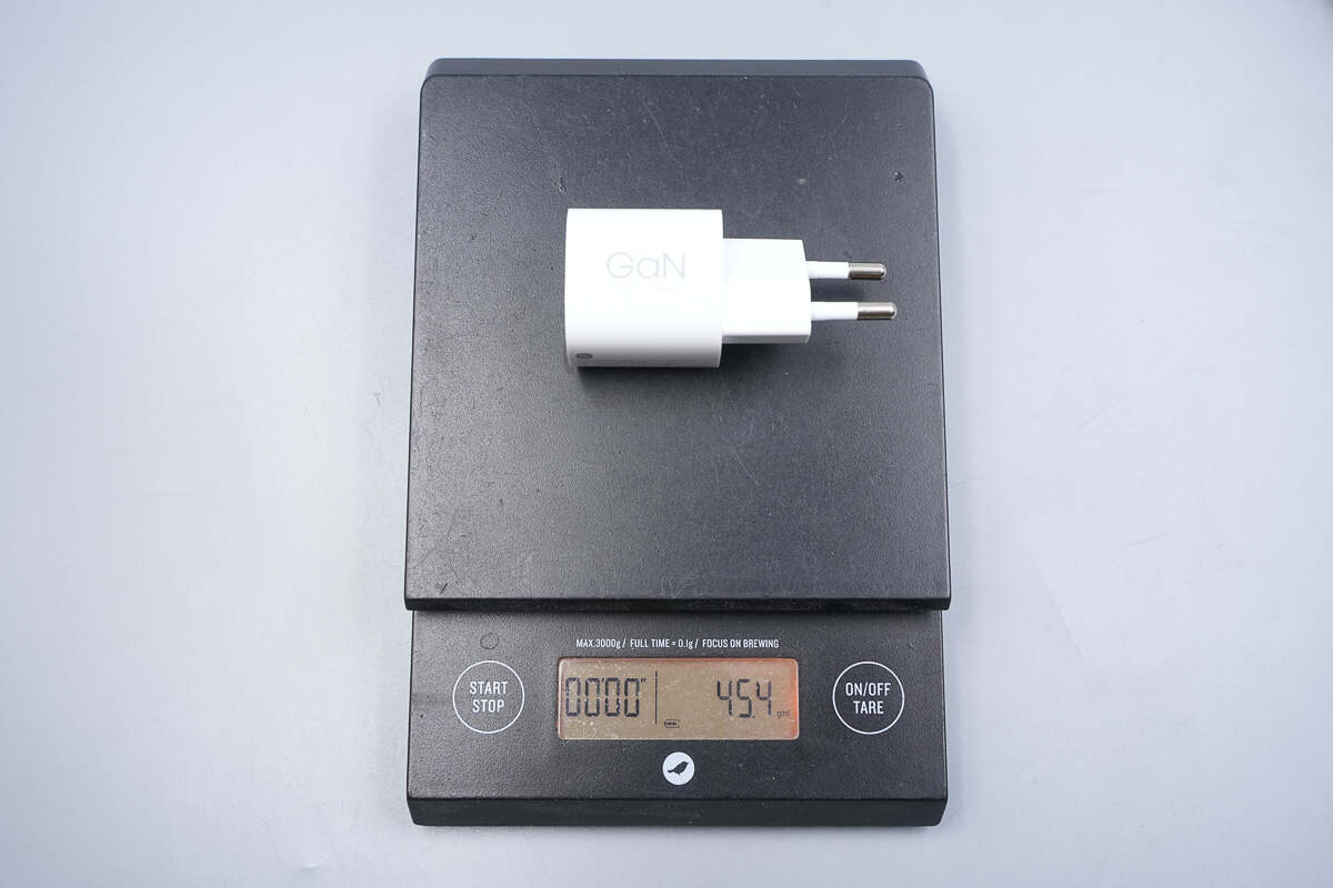
The weight is about 45 g (1.59 oz).
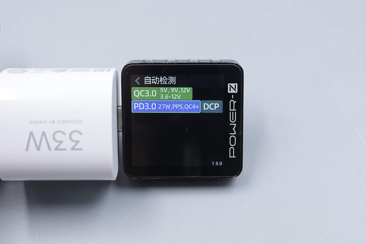
ChargerLAB POWER-Z KM003C shows that it supports QC3.0, PD3.0, PPS, and DCP protocols.

It has two fixed PDOs of 5V3A and 9V3A. It also has one set of PPS, which is 3.6-11V3A.
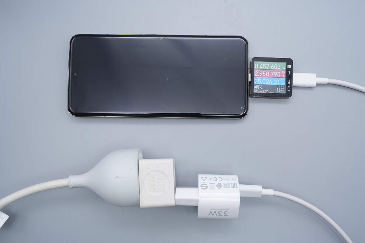
Use it to charge the Xiaomi 15 Pro, the power is about 25.02W.
Teardown
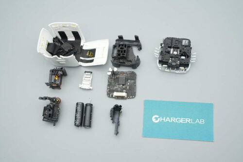
Next, let's take it apart to see its internal components and structure.

Cut open the casing to reveal the PCBA module. The input side features a contact-type power connection design.

The length of the PCBA module is about 28.3 mm (1.11 inches).

The width is about 25.56 mm (1.0063 inches).

The thickness is about 24.97 mm (0.98 inches).

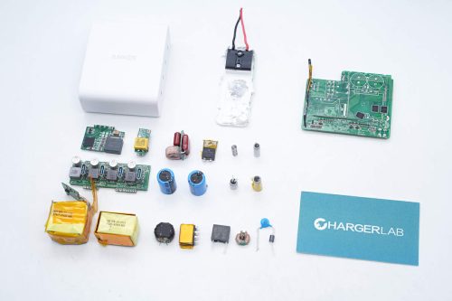
The PCBA module consists of two small PCBs. The input side is protected with foam, and components such as capacitors and the transformer are reinforced with adhesive.
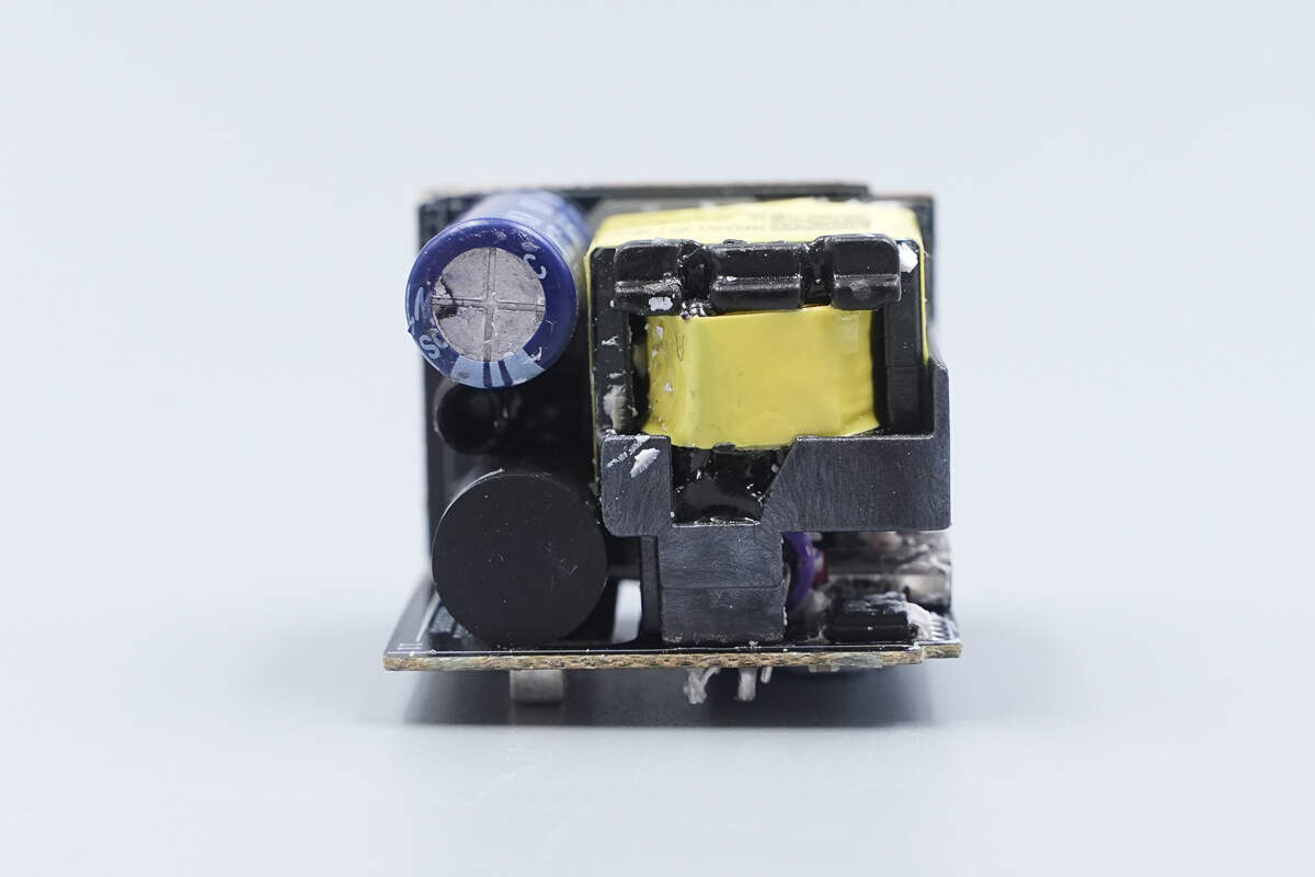
Remove the adhesive. A high-voltage filtering electrolytic capacitor is protected with a plastic sleeve, and one side of the transformer is encased in a plastic housing to provide primary-to-secondary isolation.
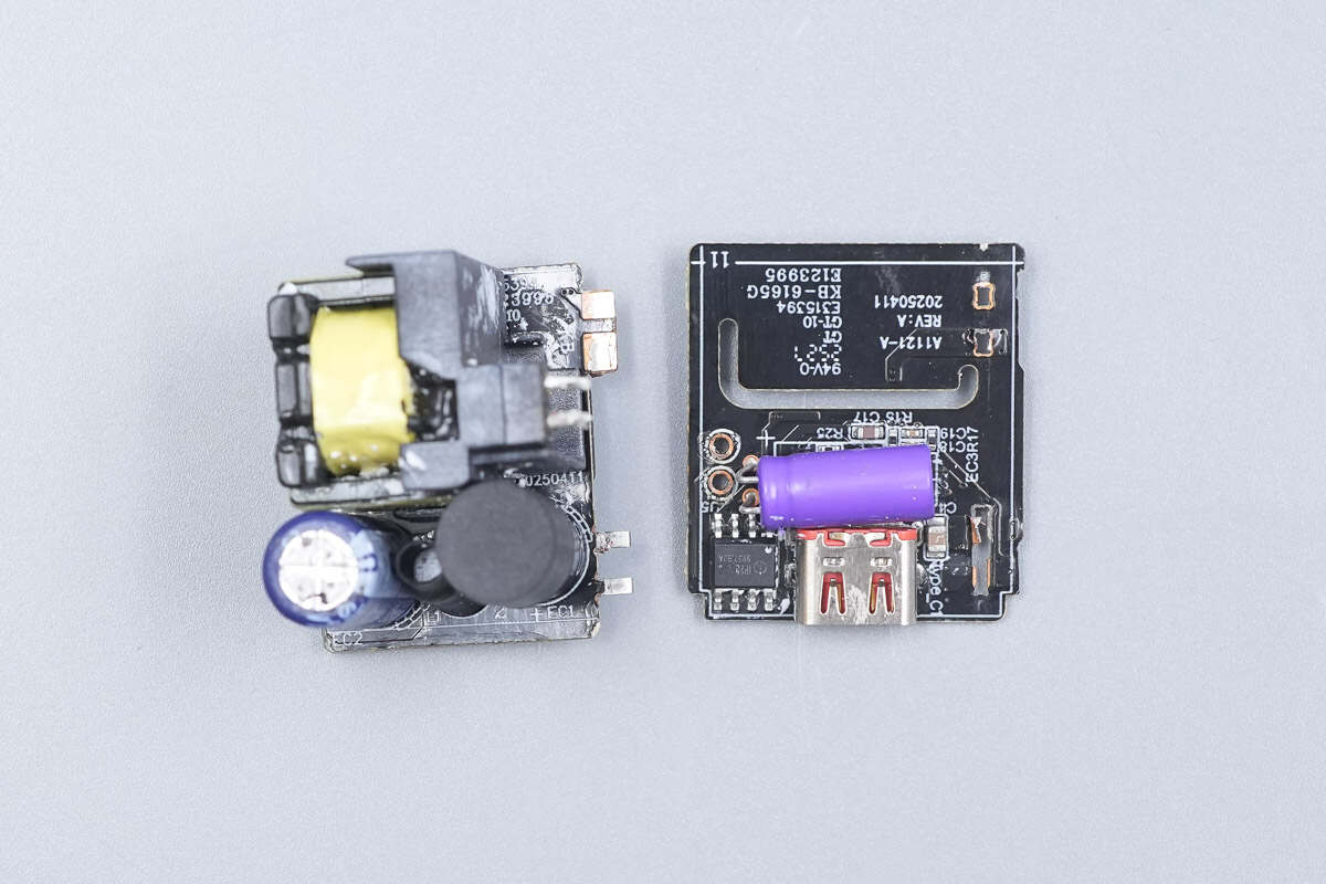
Separate the two small PCBs.
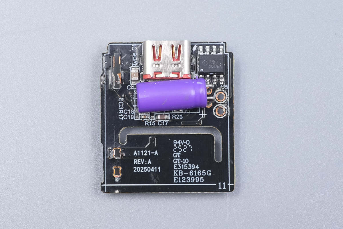
On the bottom PCB, the secondary side is equipped with a synchronous rectifier controller and a solid capacitor for output filtering.

On the back side, there is an SMD fuse, a bridge rectifier, a protocol chip, and an output VBUS MOSFET.

On the front side of the side PCB, there are electrolytic capacitors, an I-shaped inductor, and a transformer.
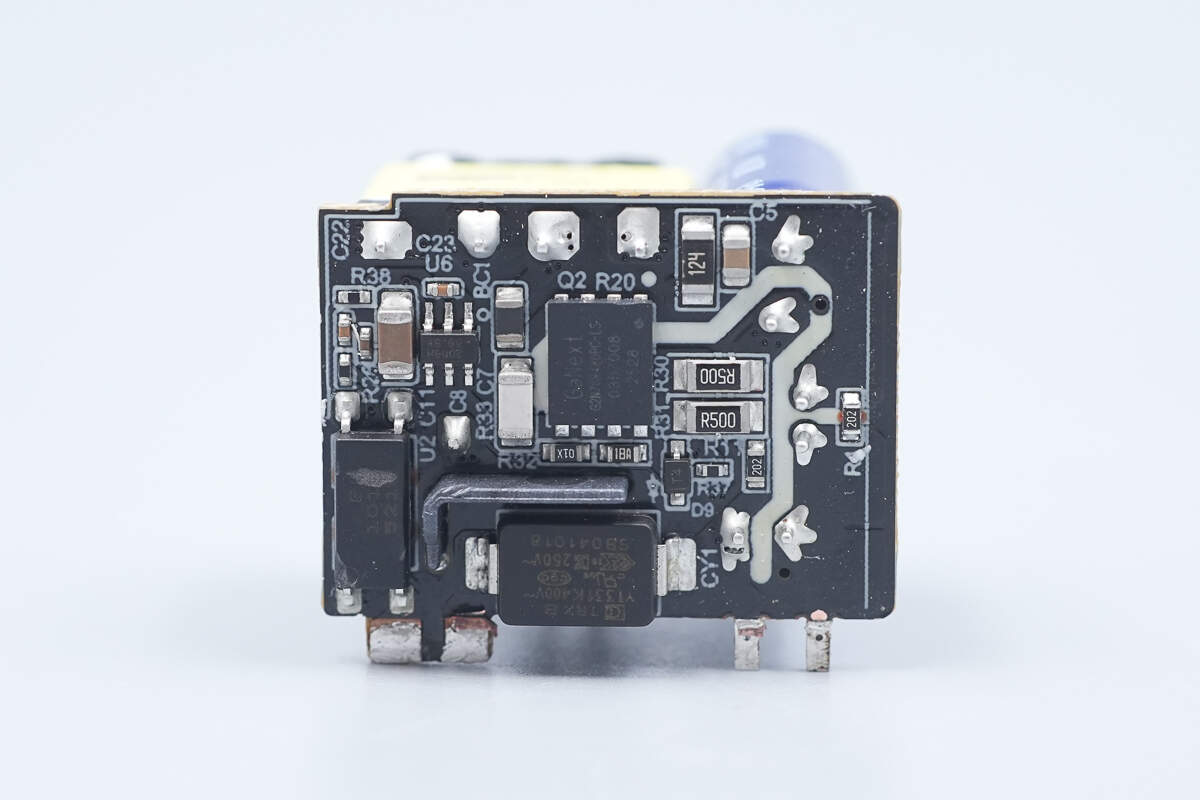
On the back side, there is a master control chip, a primary MOSFET, an optocoupler, and an SMD Y capacitor.

The SMD fuse is sourced from Betterfuse, with a rated current of 3.15 A.
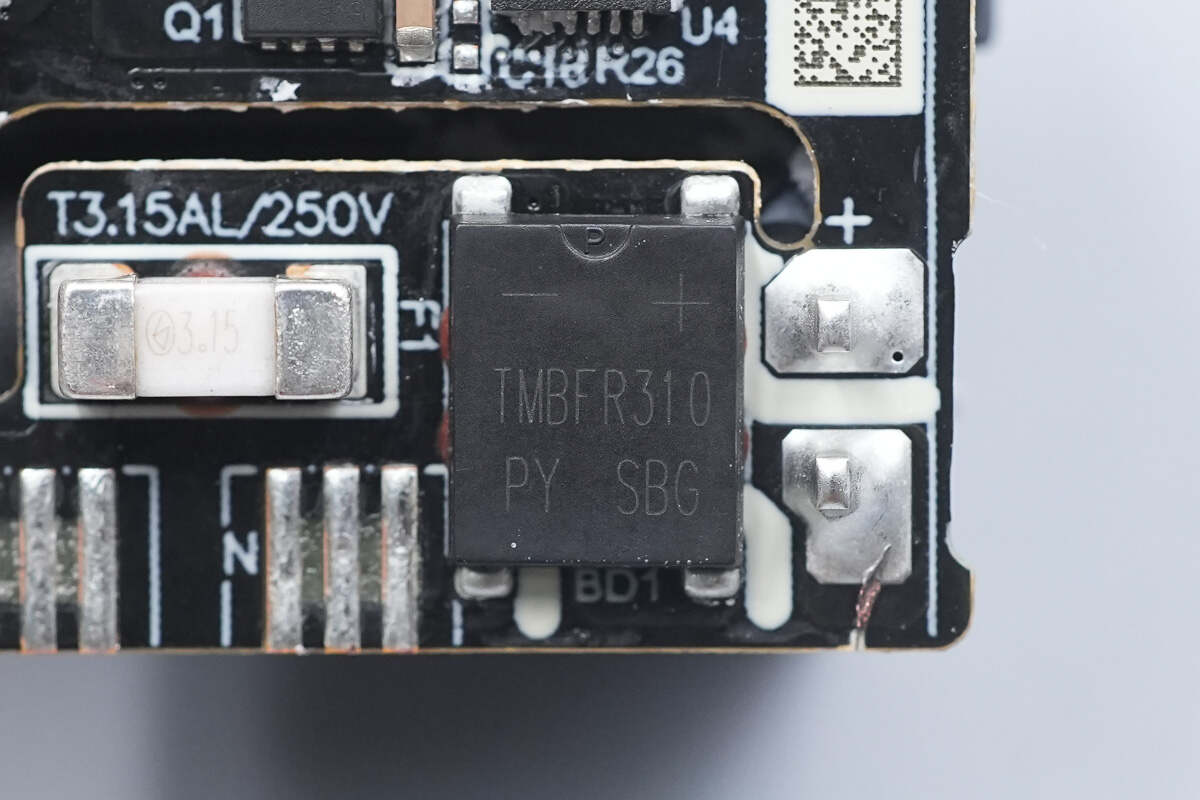
The bridge rectifier is from PY, model TMBFR310, rated at 3 A 1000 V, and comes in a TMBF package.
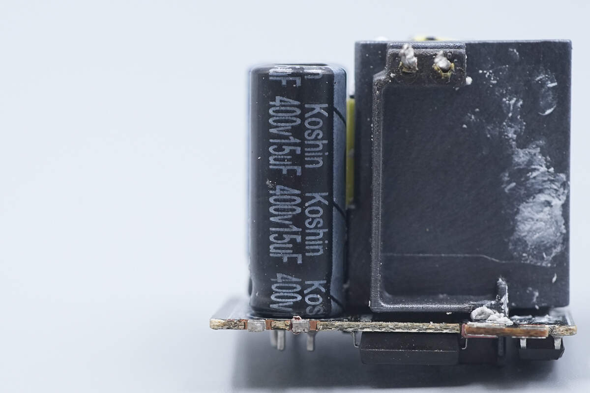
The high-voltage filtering electrolytic capacitor is from Koshin, rated at 400 V, 15 μF.
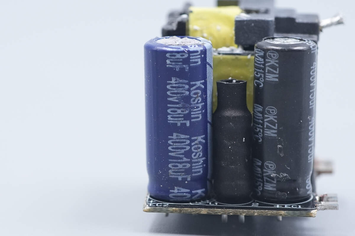
The other capacitor is also from Koshin, rated at 400 V, 18 μF.
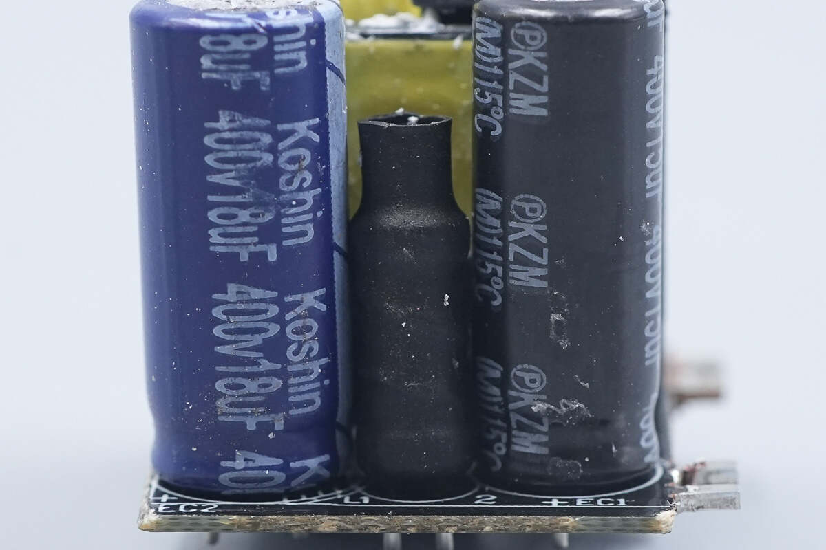
The I-shaped inductor is insulated with a heat-shrink tube for protection.
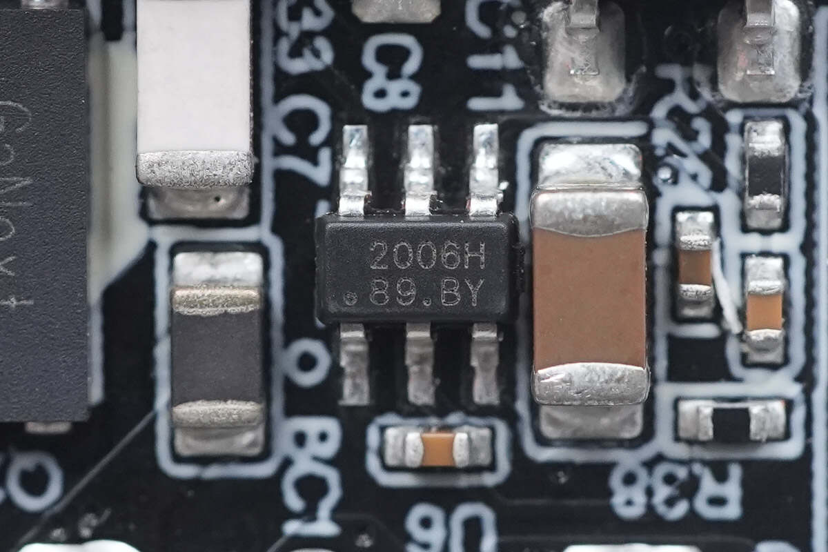
The master control chip is from Injoinic, model IP2006H. It is a high-performance multi-mode flyback controller featuring frequency foldback and valley switching technologies. It supports adaptive switching frequency to improve light-load efficiency, optimize maximum switching frequency, reduce temperature rise, and enhance full-load efficiency.
The IP2006H also supports burst mode, which lowers standby power consumption under light and no-load conditions, complying with CoC V5 and DoE Level VI standards. It offers comprehensive protection functions, including brown-in/brown-out, output overvoltage protection, output undervoltage protection, VDD overvoltage protection, input overvoltage protection, and over-temperature protection. It supports parameter customization and over-power protection and comes in a SOT23-6 package.

Here is the information about Injoinic IP2006H.
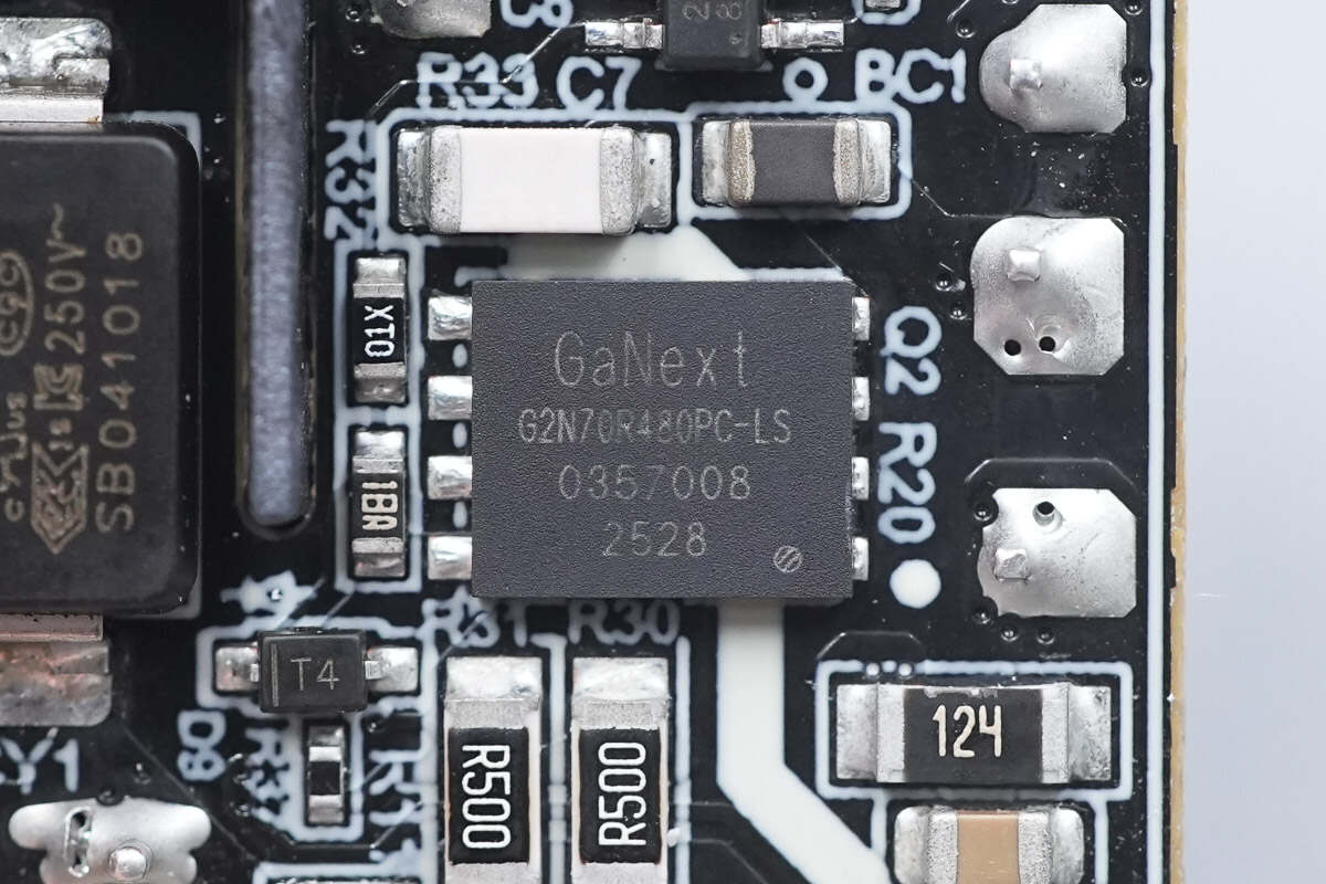
The GaN FET is from GaNext, model G2N70R480PC-LS. It is a 700 V GaN power device with a transient voltage rating of 800 V, a nominal on-resistance of 480 mΩ, and a gate voltage tolerance of ±20 V. It comes in a DFN5×6-8L package.
The G2N70 series FET is a hybrid normally-off GaN power device, featuring one of the most robust gate structures and the lowest reverse voltage drop among wide-bandgap semiconductors worldwide. This series supports a simple gate drive scheme while delivering industry-leading performance and excellent reliability.

Here is the information about GaNext G2N70R480PC-LS.
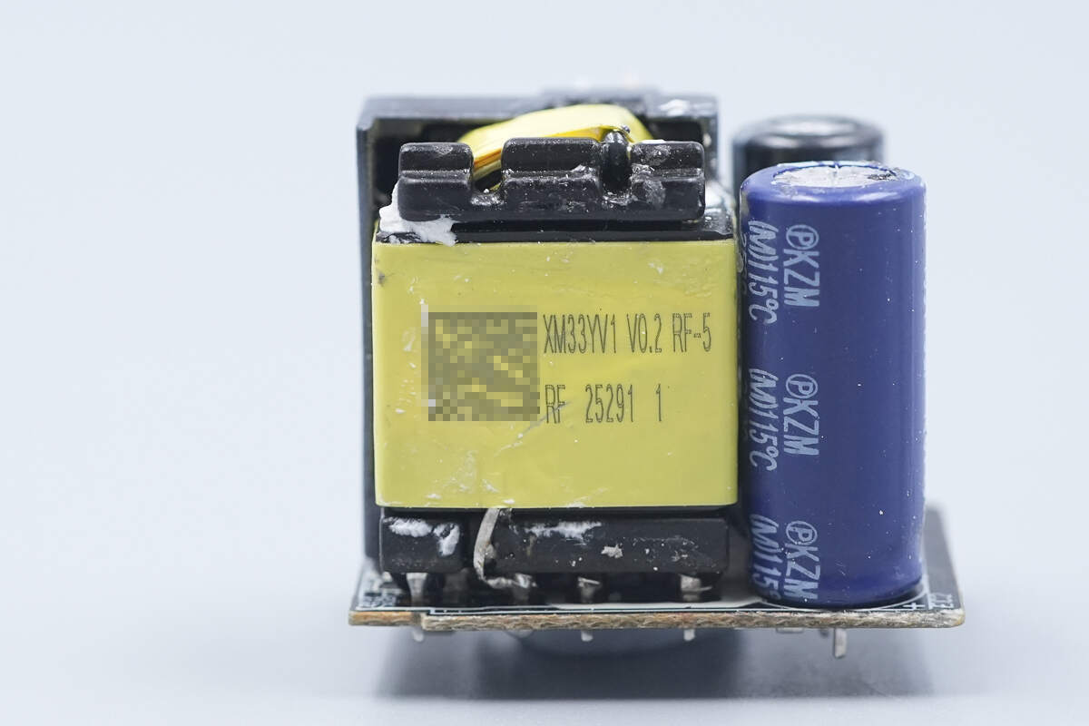
Close-up of the transformer.

An Everlight optocoupler is used for output voltage feedback; any wear marks are caused by casing disassembly.
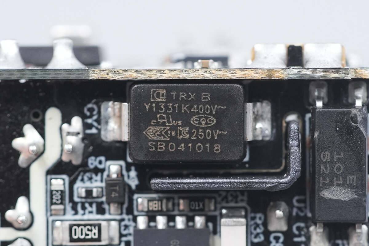
The SMD Y capacitor is from TRX, part number TMY1331K. Its compact size and light weight make it well-suited for high-density power products such as GaN fast chargers.
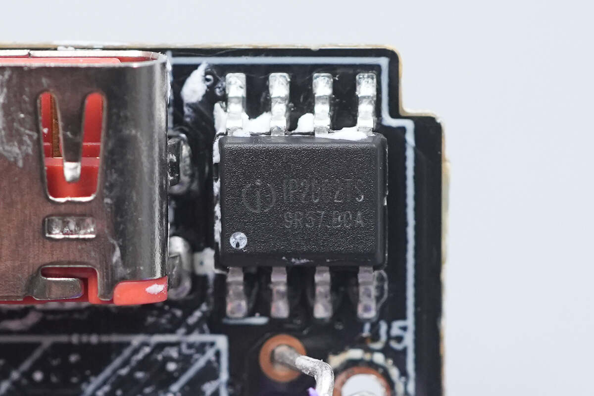
The synchronous rectifier controller is from Injoinic, model IP2002TS. It is a synchronous rectification controller with an integrated 65 V MOSFET, designed to replace Schottky diodes in high-efficiency flyback power supplies. By monitoring the drain-to-source voltage of the SR MOSFET, the IP2002TS can generate optimal drive signals to turn the MOSFET on or off. Synchronous rectification effectively reduces power loss on the secondary-side rectifier, achieving higher efficiency and increased power density.
The IP2002TS requires minimal external components to provide a high-performance solution for output voltages between 3.3 V and 12 V. It does not require an auxiliary winding for power; the internal regulation circuit generates its own supply voltage. This makes it suitable for charger applications with low output voltage requirements or adapters using a high-side synchronous rectification scheme.

To ensure rapid MOSFET turn-off capability, as the secondary current decreases, the IP2002TS reduces the MOSFET drive voltage to adjust the MOSFET’s conduction voltage drop to approximately 40 mV, and quickly turns it off before the drain-to-source voltage reverses. A configurable ringing detection circuit prevents false turn-on caused by V<sub>DS</sub> ringing in discontinuous conduction mode (DCM) and quasi-resonant operation. The IP2002TS comes in an SOP-8L package.
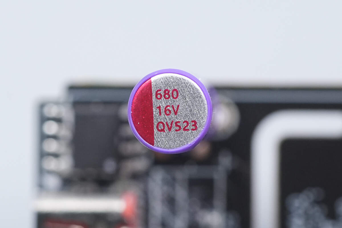
The solid capacitor for output filtering is from PolyCap, rated at 16 V, 680 μF.
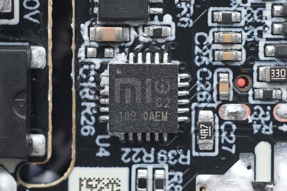
The protocol chip is custom-designed by Injoinic for Xiaomi. The chip is marked with both the Xiaomi and Injoinic logos and also bears the designation “C2.”
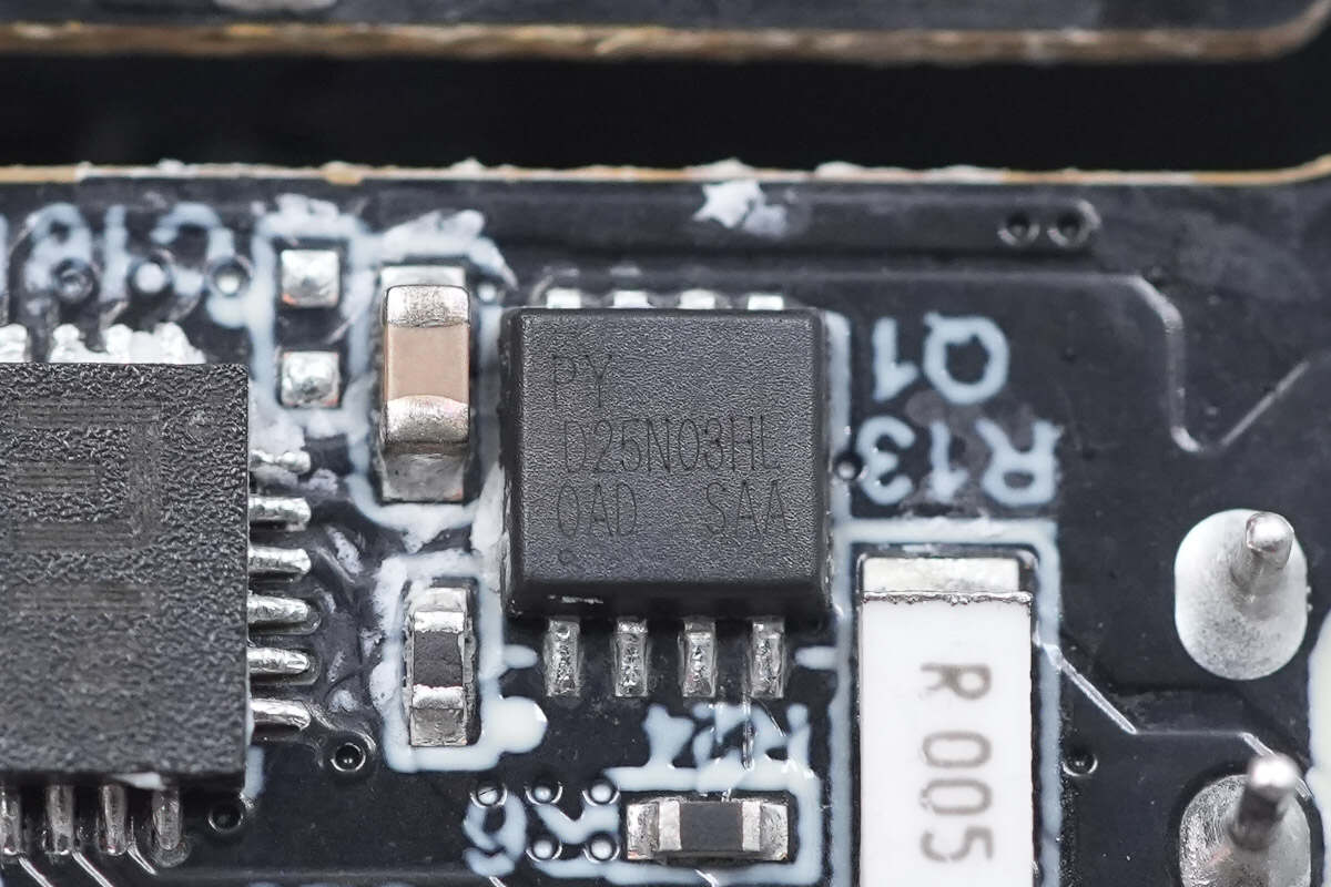
The output VBUS MOSFET is from PY, model D25N03HL. It is an NMOS with a voltage rating of 30 V, an on-resistance of 10 mΩ, and comes in a DFN3×3 package.

The USB-C socket is soldered through plated-through holes.

Well, those are all components of the Xiaomi 33W Nano Power Adapter.
Summary of ChargerLAB

Here is the component list of the Xiaomi 33W Nano Power Adapter for your convenience.
It features a compact and rounded design with a European-standard plug, supports 100–240 V global wide-voltage input, and is compatible with PD, PPS, and QC fast-charging protocols, meeting the fast-charging requirements of Xiaomi, Apple, Samsung, and other smartphones.
After taking it apart, we found that it is designed based on the Injoinic IP2006H + IP2002TS high-frequency QR flyback power solution. It also uses a custom Injoinic protocol chip to control the output. The GaN power device is the GaNext G2N70R480PC-LS, while the capacitors are sourced from Koshin and PolyCap. The PCBA module is reinforced with adhesive. Isolation is implemented between the primary and secondary sides. Overall, the build quality and component selection are excellent.
Related Articles:
1. Teardown of UGREEN 22.5W 20000mAh Power Bank with Built-in Cable (PB505)
2. Teardown of EcoFlow RAPID Pro 320W GaN Desktop Charger (EF-DC-320)
3. Teardown of MEGMEET 600W Switching Power Supply (MSP600)