Introduction
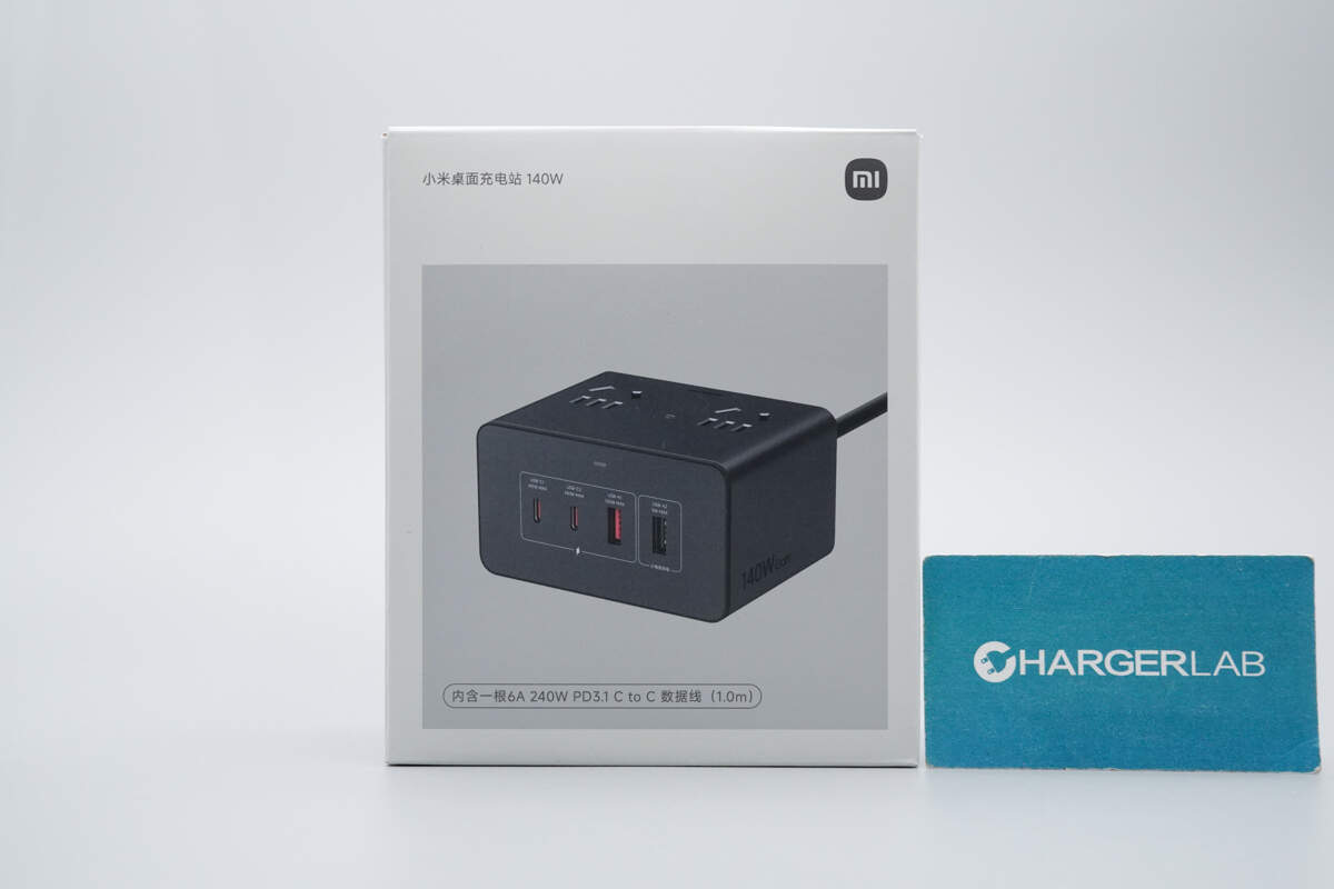
Xiaomi has recently launched a 140W 8-in-1 GaN desktop charging station. The front panel features an AG coating combined with an optical coating process, delivering a refined tactile feel while effectively resisting fingerprints and stains. Two USB-C ports and one of the USB-A ports support Xiaomi’s proprietary 120W HyperCharge protocol. In addition, both USB-C ports support PD 3.1 with a maximum output of 140W.
The USB-A1 port also supports up to 100W PD, offering broad compatibility with a wide range of devices. A dedicated USB-A2 port is designed with a low-current charging mode for devices such as earbuds and smartwatches. Next, through a detailed teardown, we will take a closer look at its internal design and component selection.
Product Appearance
The front of the packaging features the Xiaomi logo, product name, and images of the product's appearance.
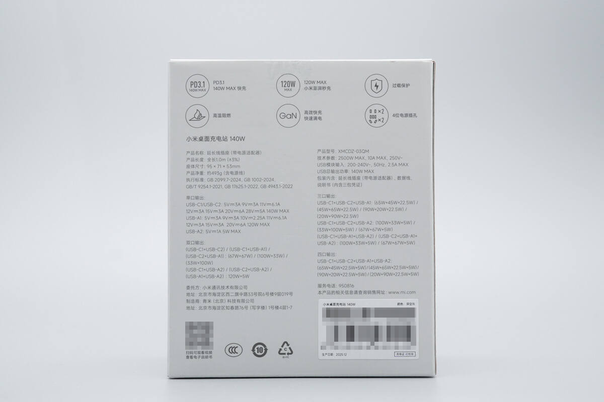
The back of the packaging displays key selling points, product specifications, and vendor information.
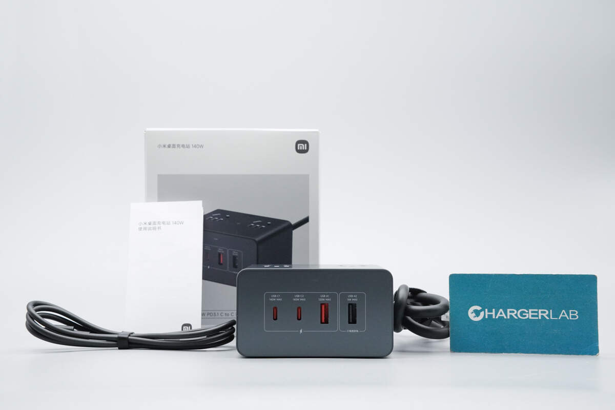
The package includes the Xiaomi 140W Desktop Charging Station, a data cable, and a user manual.
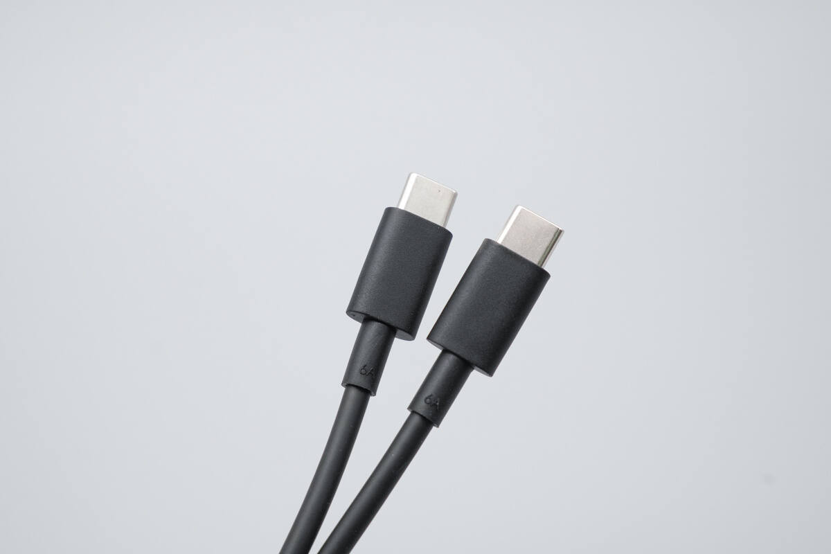
The included data cable is a dual USB-C type, with matte-finished connectors. The cable’s tail features a "6A" marking, indicating its current rating.
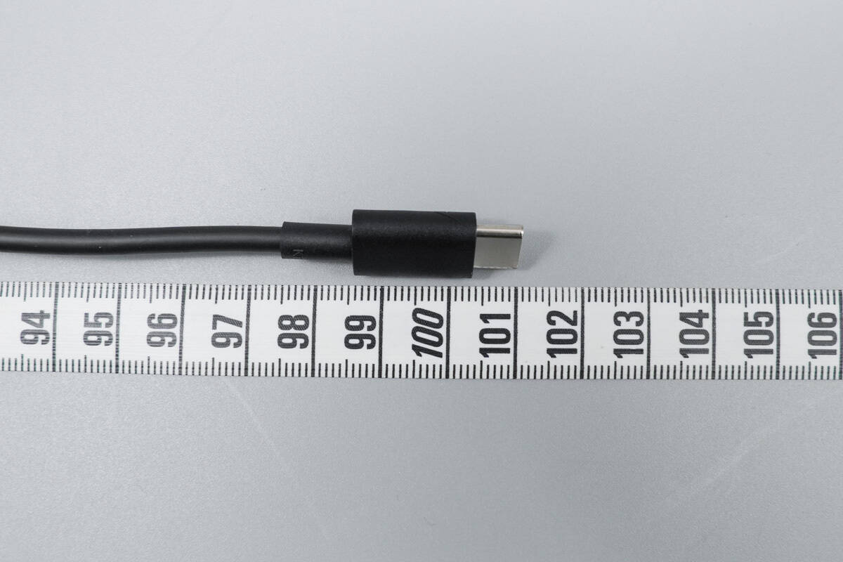
The length of the cable is about 101 cm (39.76 inches).
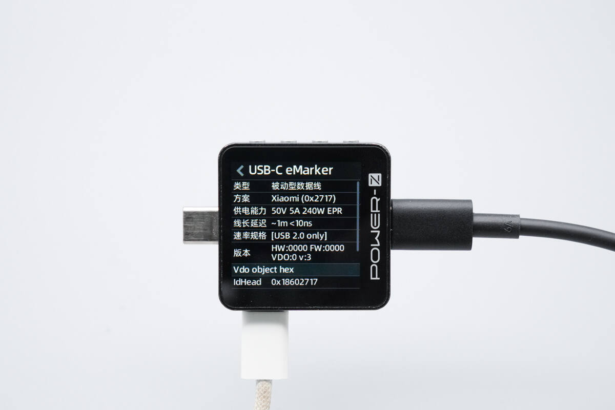
ChargerLAB POWER-Z KM003C indicates that the cable is equipped with an E-Marker chip, with a power transmission capability of 50V 5A. It also supports data transmission at USB 2.0 speeds.
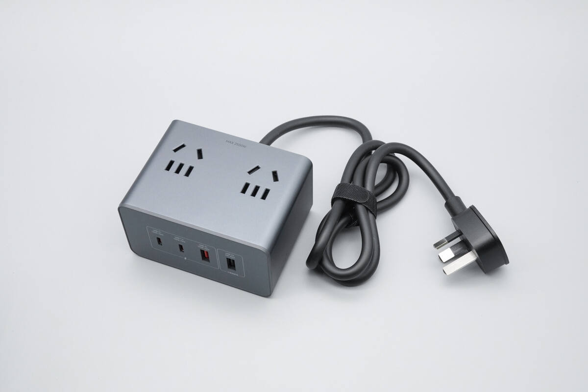
It is equipped with a power cord with a three-prong plug.

The inner side of the plug is labeled with the brand and relevant specifications, which are 10A 250V~, and it has passed the CCC certification.
The outer casing is made of PC flame-retardant material.
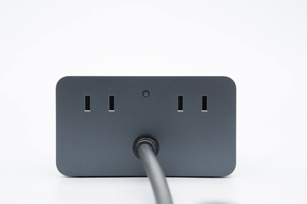
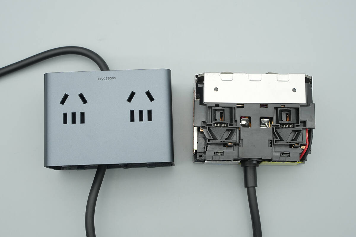
The connection between the power cord and the main body is protected by a rubber sleeve. The back of the charging station features two sets of dual-prong AC outlets.
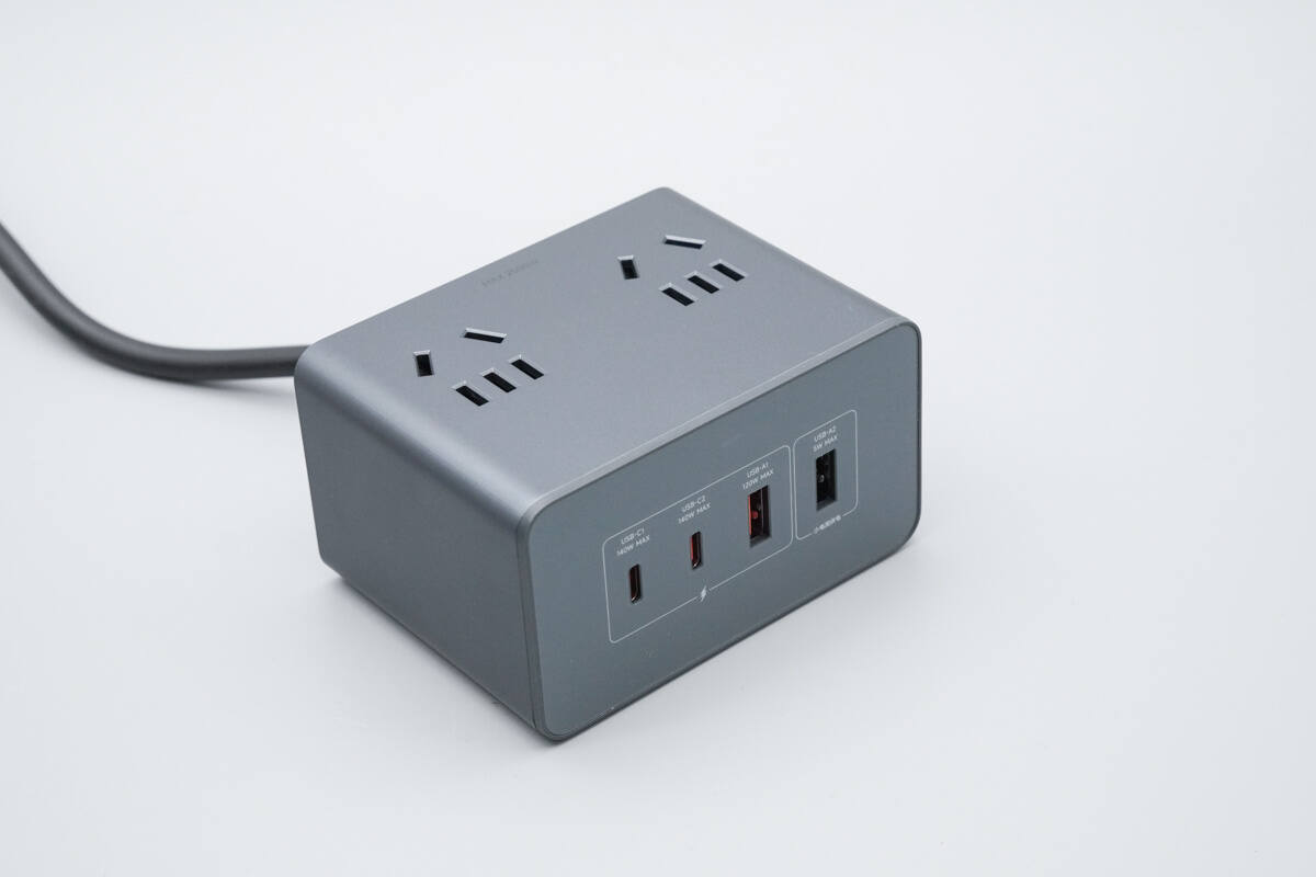
An overload protection button is provided between the sockets.
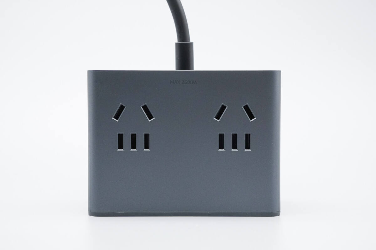
The top is equipped with two sets of 3+2 combination sockets, with "MAX 2500W" marked on the edge, indicating the total load capacity.
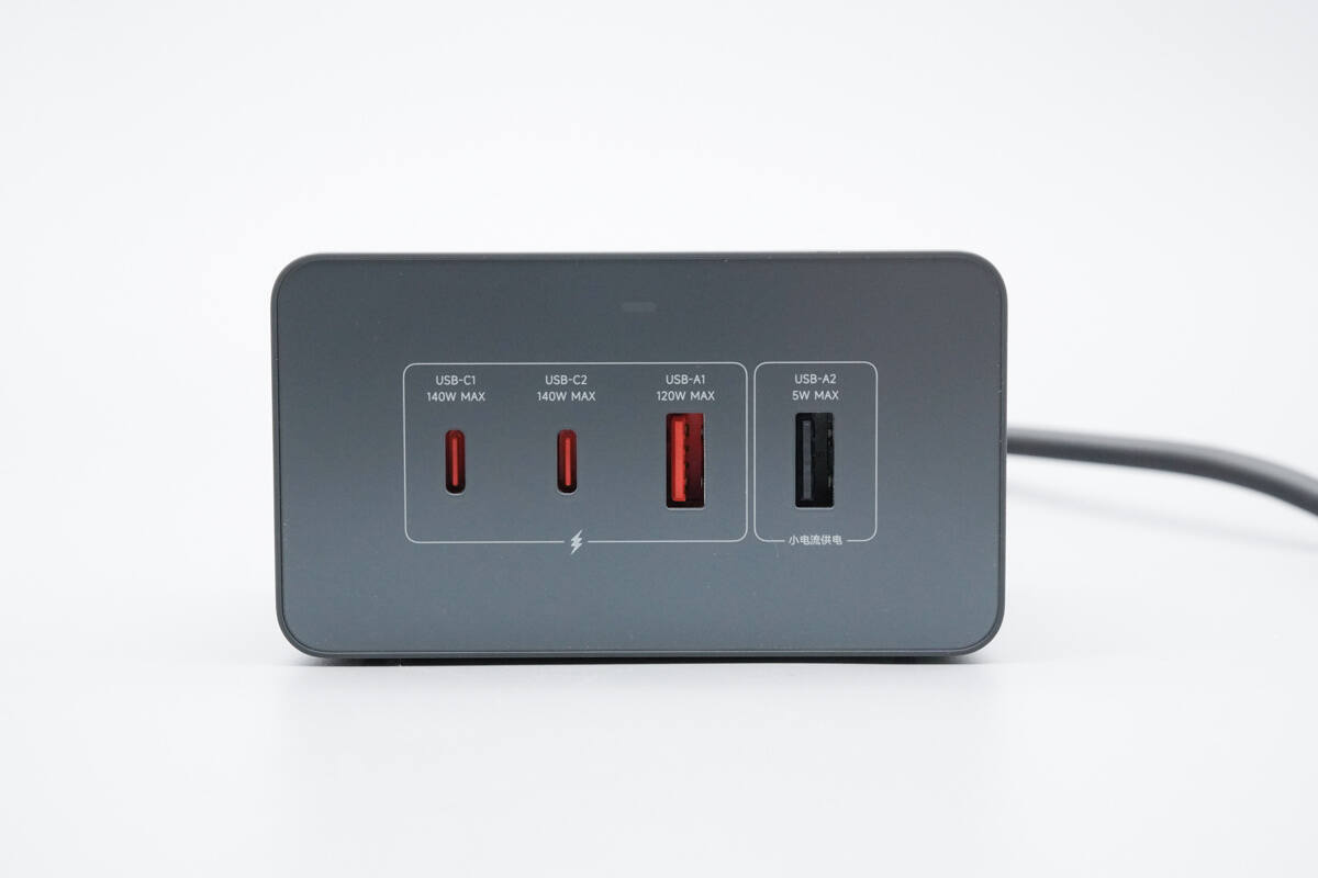
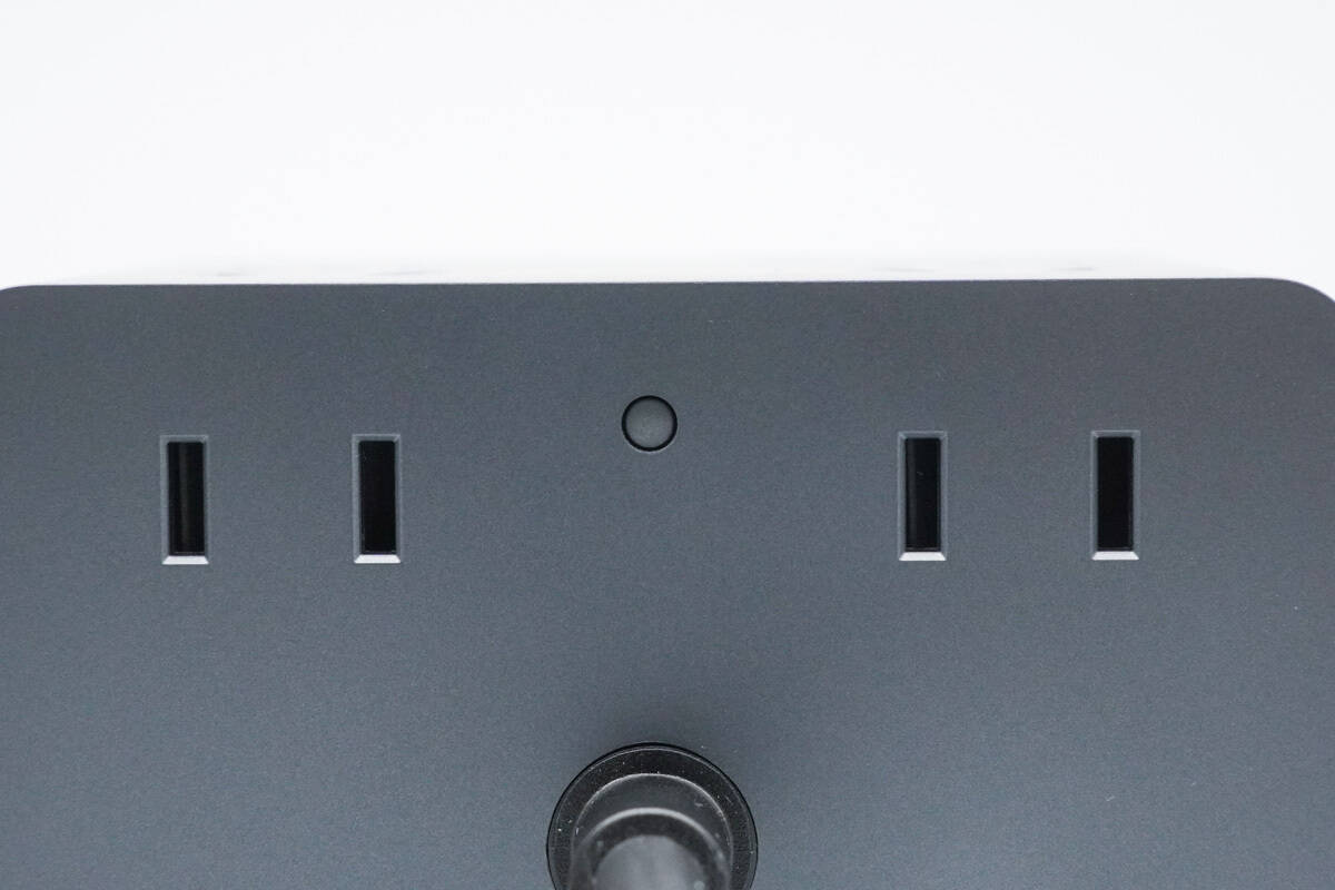
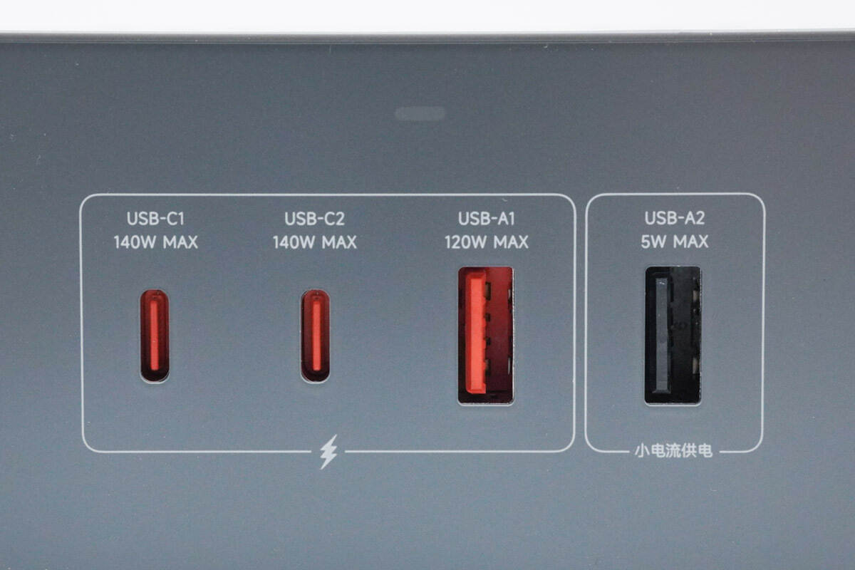
The front panel features two USB-C and two USB-A ports, each labeled with its corresponding identifier and output specifications.
An indicator light is positioned above the ports.
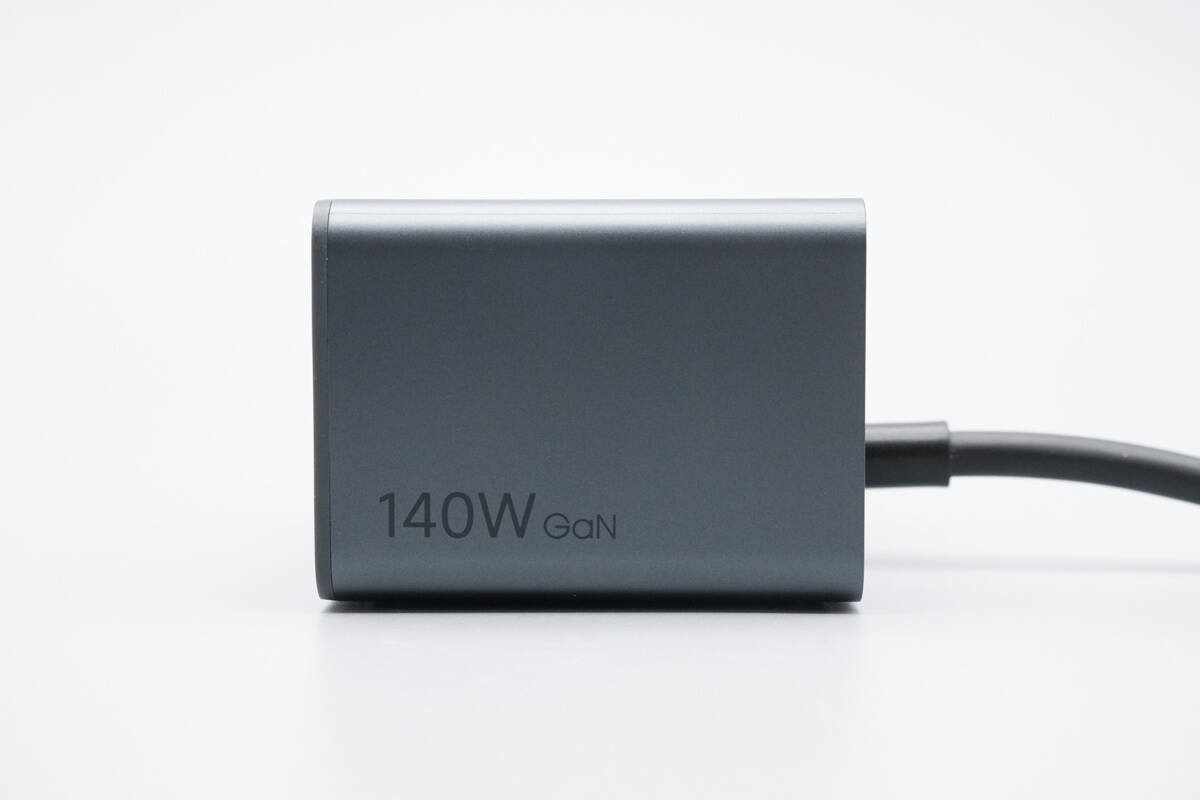
"140W GaN" is printed on one side of the device.
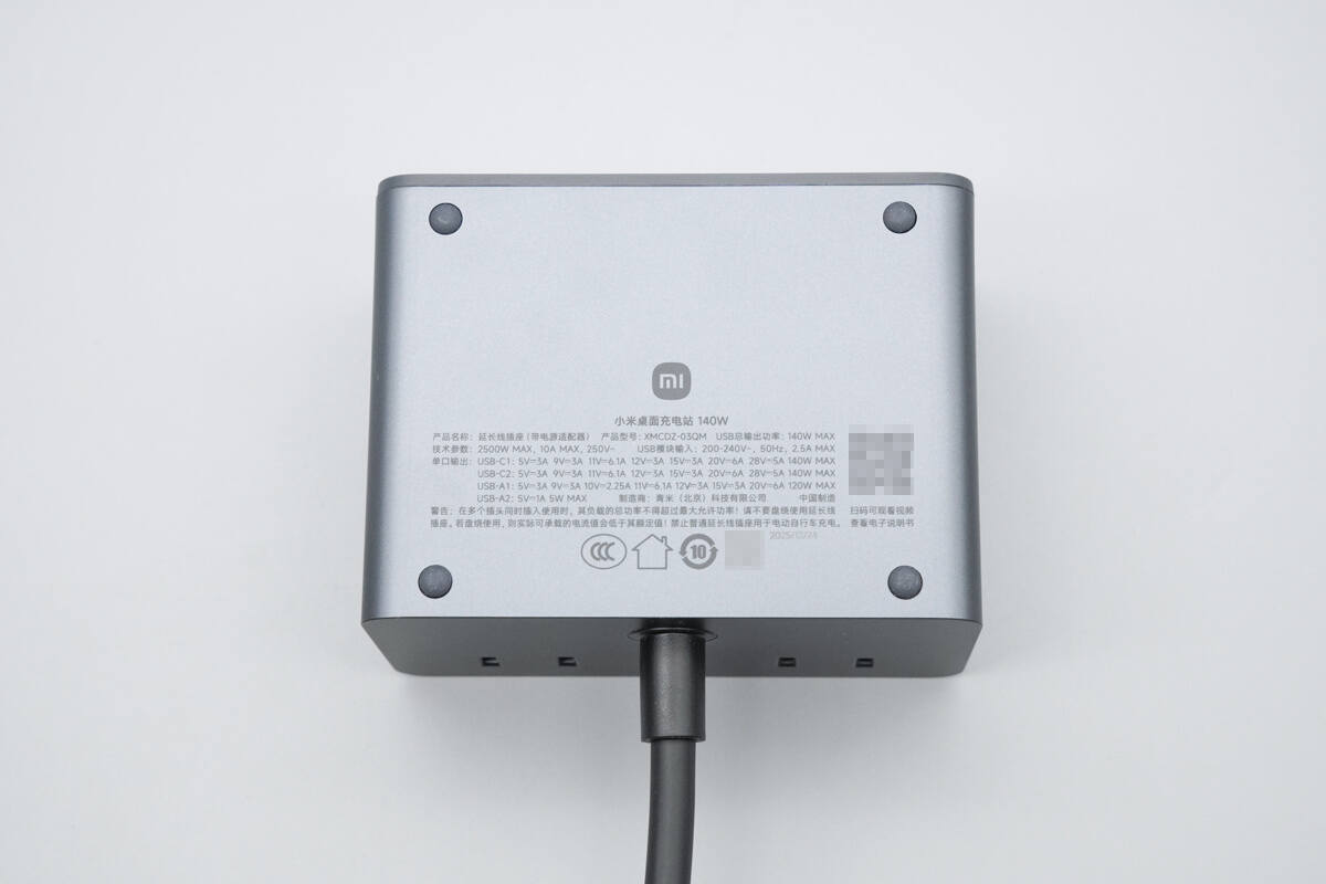
The bottom corners are equipped with anti-slip pads, and the specifications are printed on the outer casing.
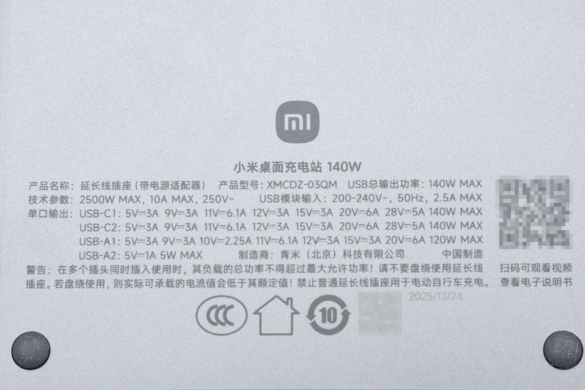
Model: XMCDZ-03QM
Technical Specifications: 2500W MAX, 10A MAX, 250V~
Total USB Output Power: 140W MAX
USB Module Input: 200-240V~, 50Hz, 2.5A MAX
Single Port Output:
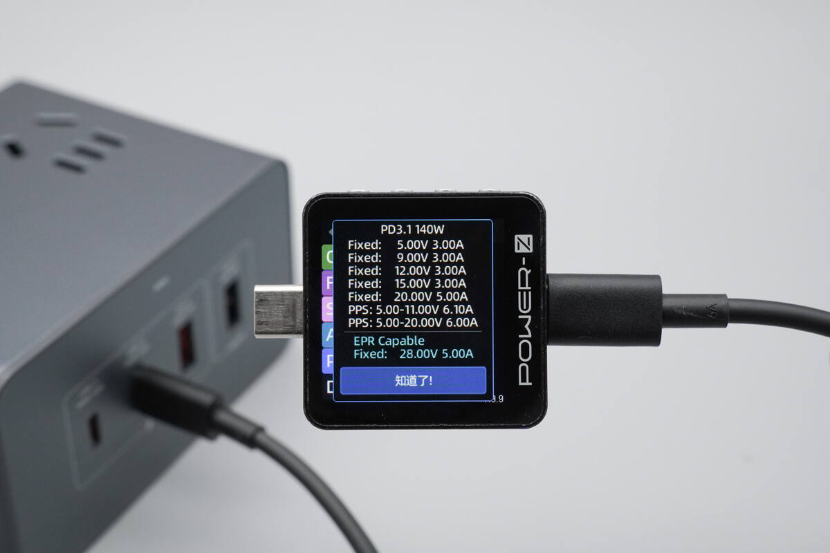
USB-C1: 5V3A, 9V3A, 11V6.1A, 12V3A, 15V3A, 20V6A, 28V5A 140W MAX
USB-C2: 5V3A, 9V3A, 11V6.1A, 12V3A, 15V3A, 20V6A, 28V5A 140W MAX
USB-A1: 5V3A, 9V3A, 10V2.25A, 11V6.1A, 12V3A, 15V3A, 20V6A 120W MAX
USB-A2: 5V1A 5W MAX
The product has passed CCC certification.
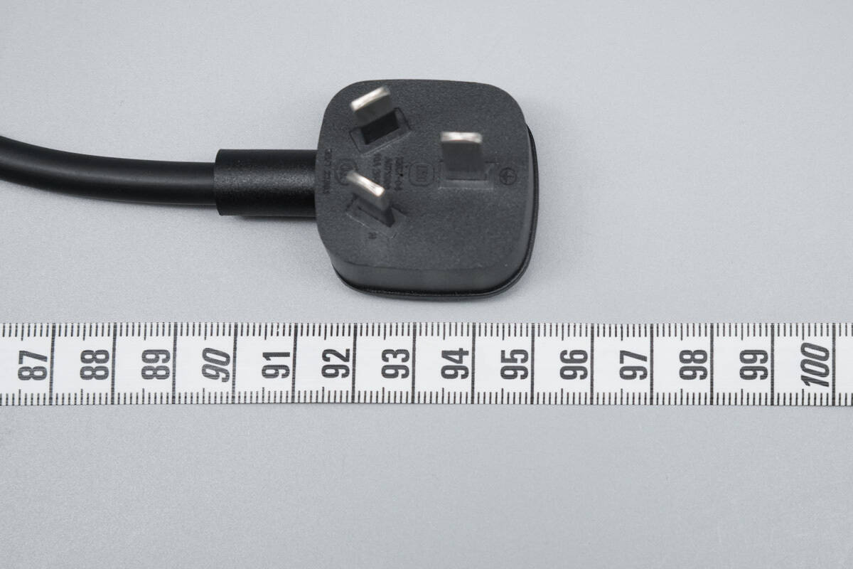
The length of the power cord is about 95 cm (39.76 inches).
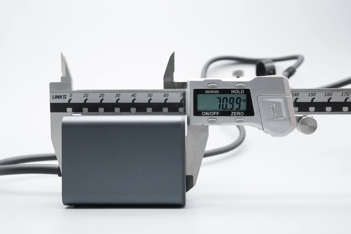
The length of the charging station is about 70.99 mm (2.79 inches).
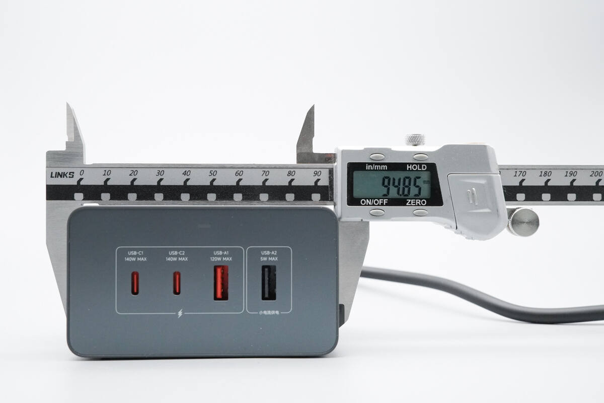
The width is about 94.85 mm (3.73 inches).
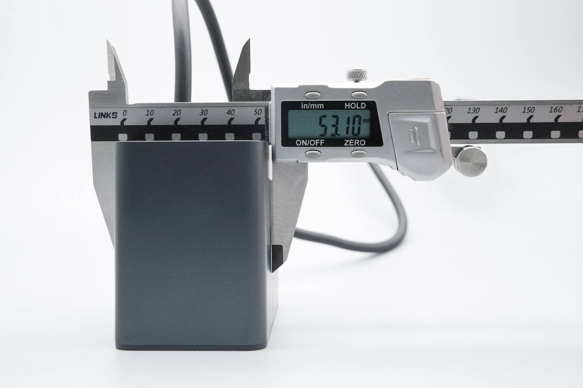
The thickness is about 53.1 mm (2.091 inches).
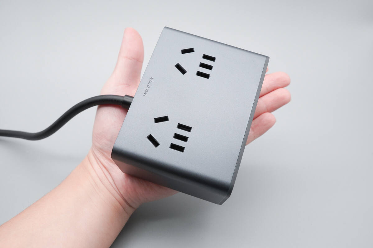
That's how big it is on the hand.
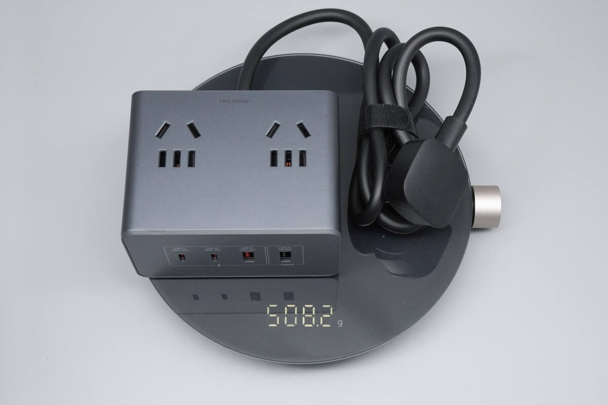
The weight is about 508 g (17.92 oz).
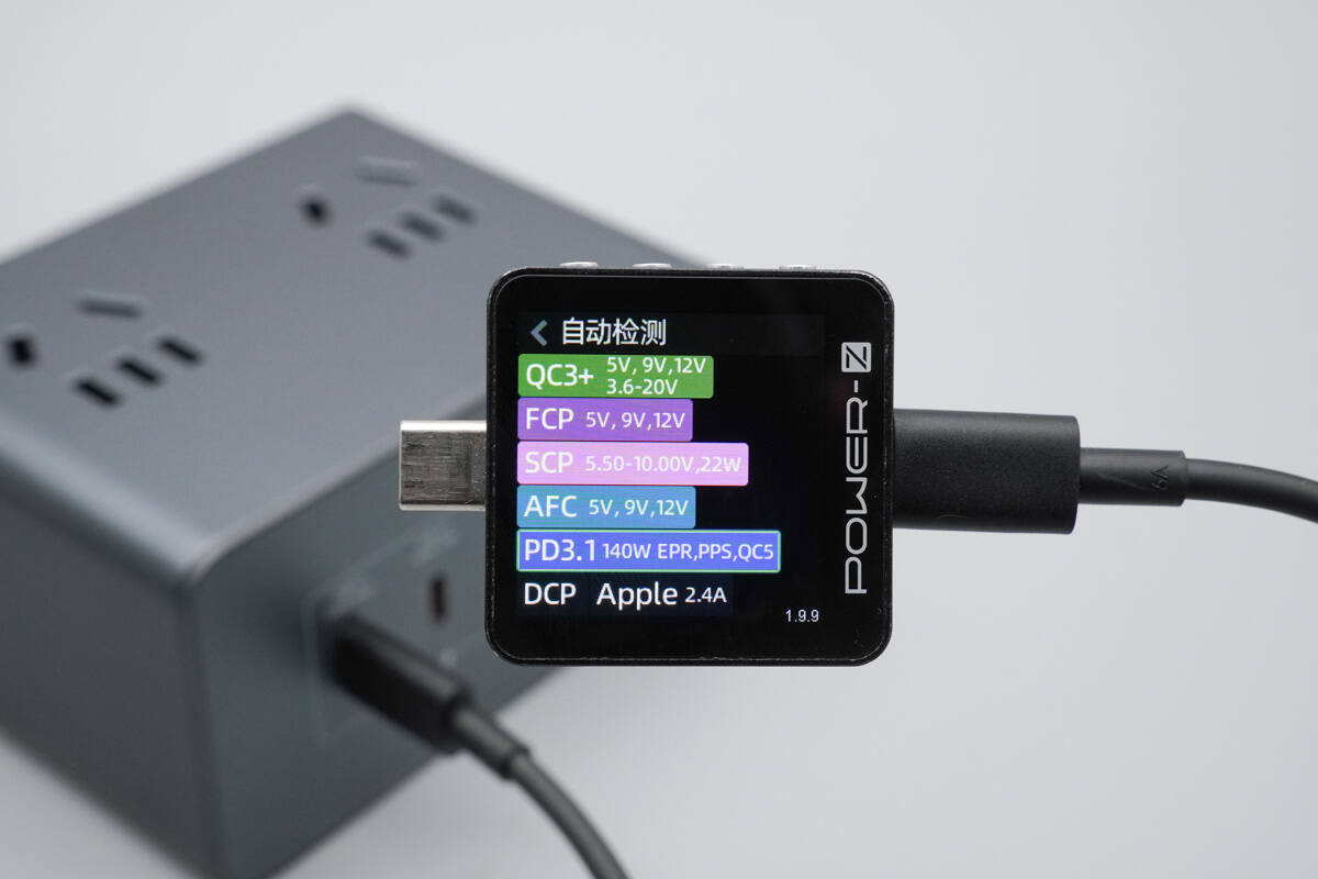
The USB-C1 supports QC3+/5, FCP, SCP, AFC, PD3.1, PPS, DCP, and Apple 2.4A charging protocols.
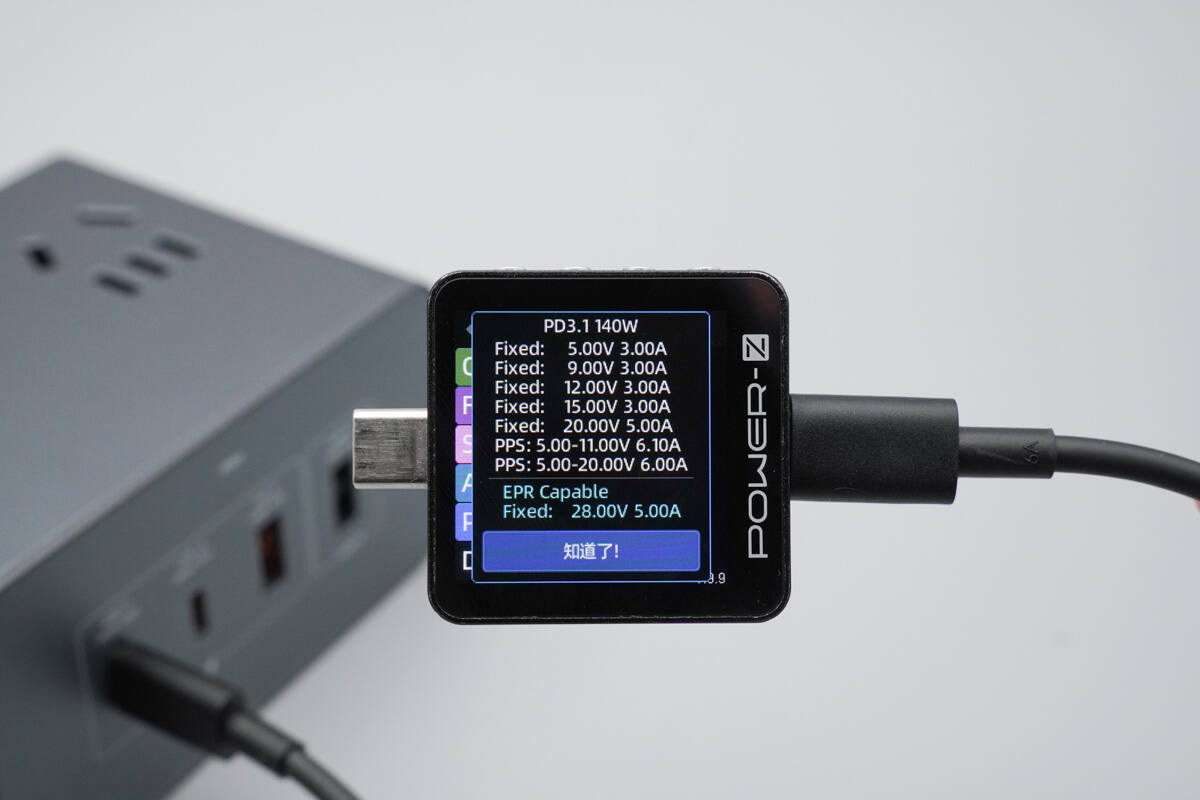
It features six fixed PDOs of 5V3A, 9V3A, 12V3A, 15V3A, 20V5A, and 28V5A. It also supports two sets of PPS, which are 5-11V6.1A and 5-20V6A.
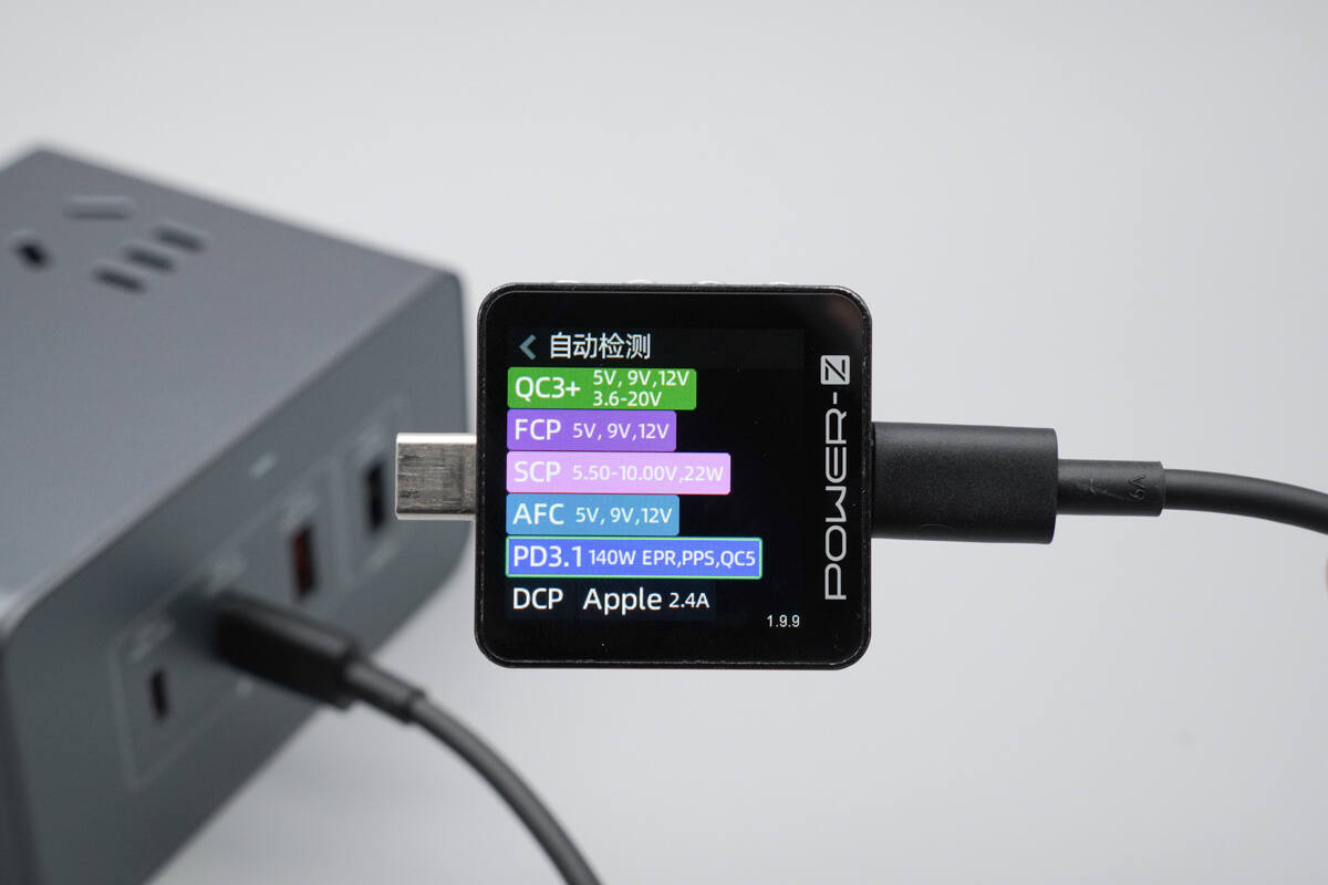
The protocols compatible with the USB-C2 port are the same as those of the USB-C1 port.
The PDO messages are also identical.
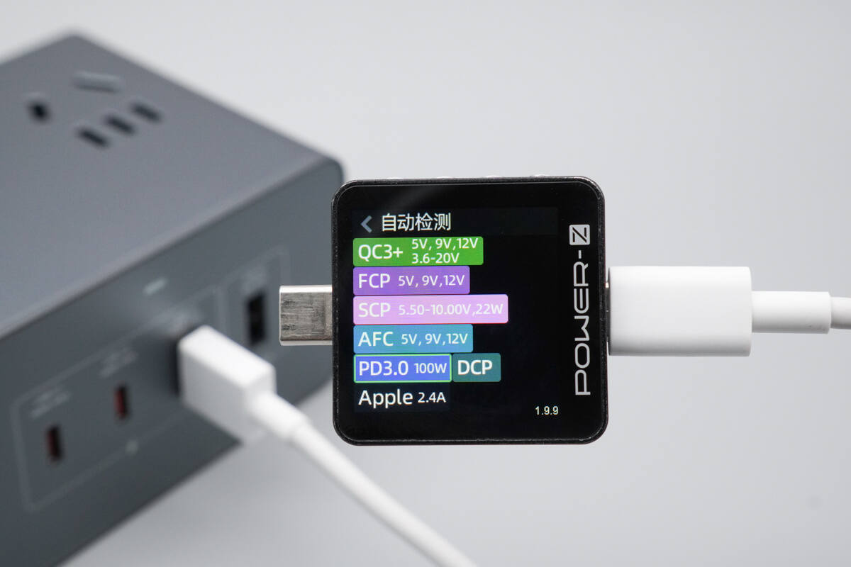
The USB-A1 supports QC3+, FCP, SCP, AFC, PD3.0, DCP, and Apple 2.4A charging protocols.
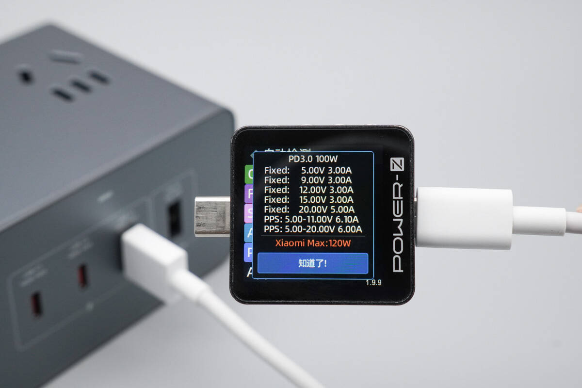
It features five fixed PDOs of 5V3A, 9V3A, 12V3A, 15V3A, and 20V5A. It also supports two sets of PPS, which are 5-11V6.1A and 5-20V6A. Additionally, it supports Xiaomi's 120W Surge Fast Charging.
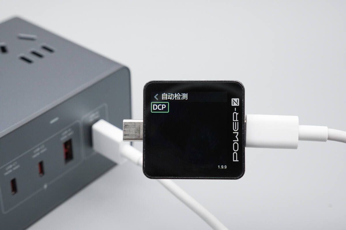
The USB-A2 supports the DCP charging protocol.
Teardown
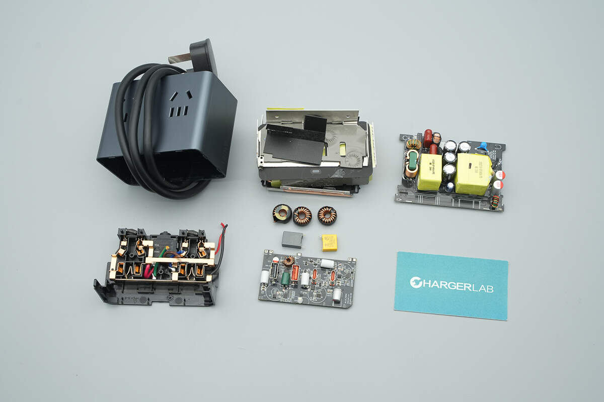
Next, let's take it apart to see its internal components and structure.
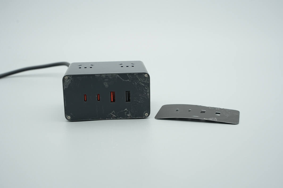
The front panel is secured with double-sided tape, and four screws are installed at the internal corners.
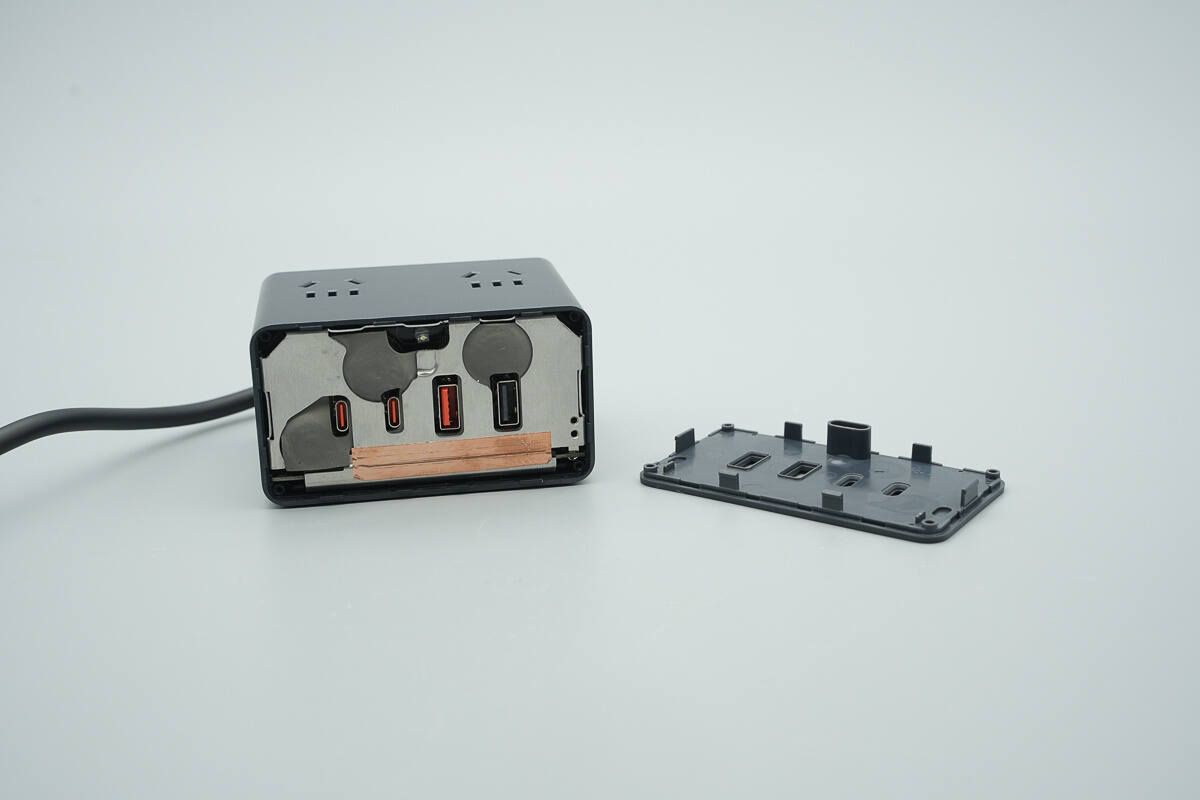
After removing the screws, the inner cover can be opened, which is also secured with clips.
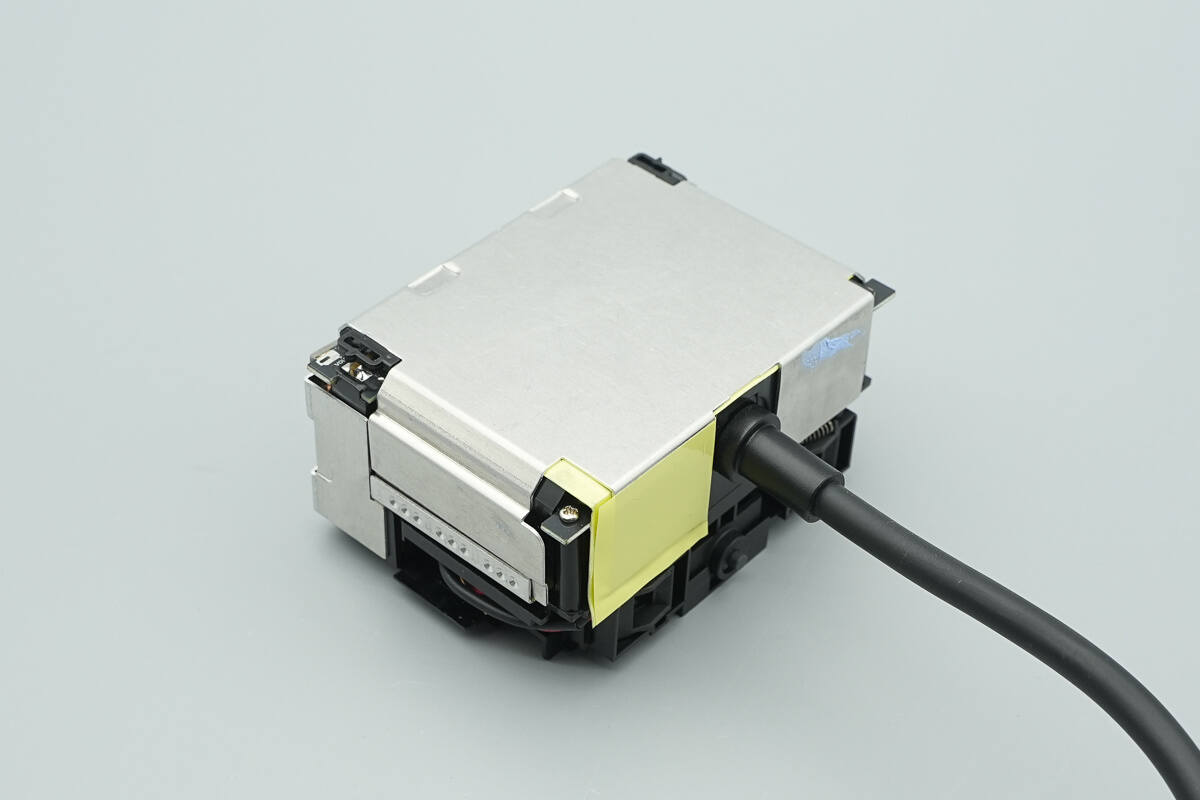
Pull out the internal module.
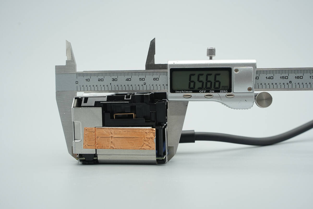
The length of the PCBA module is about 65.66 mm (2.59 inches).
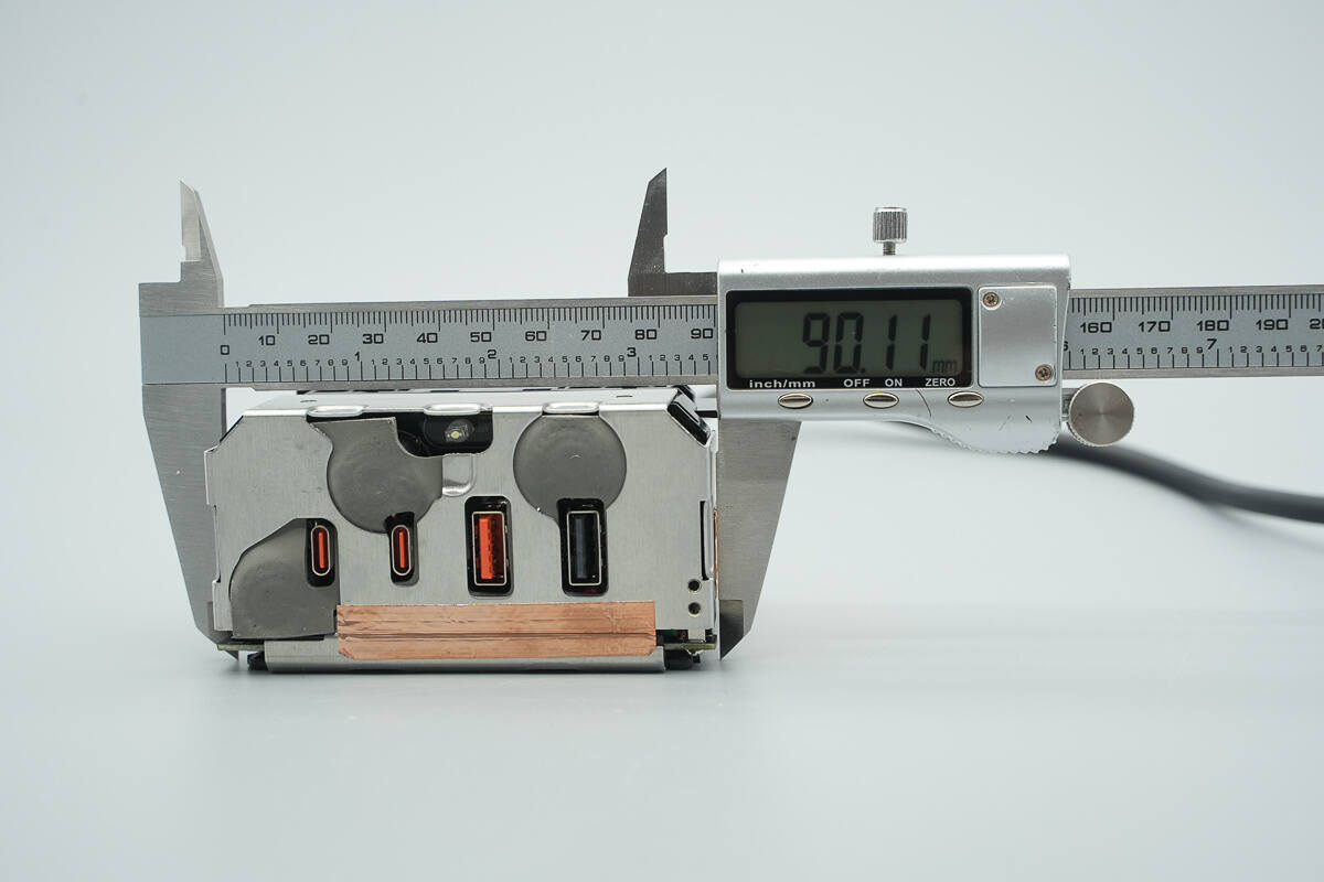
The width is about 90.11 mm (3.55 inches).

The thickness is about 49.14 mm (1.93 inches).
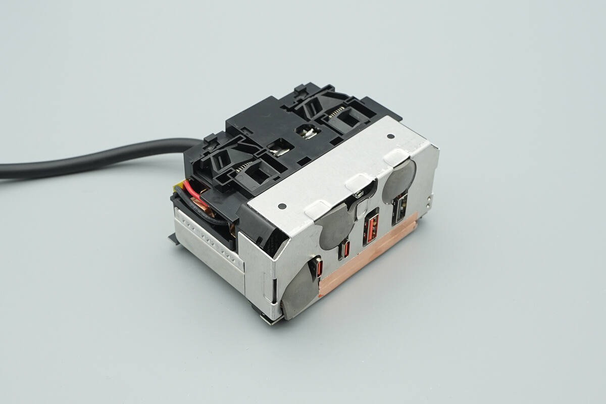
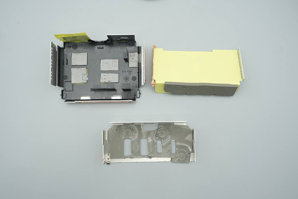
The bottom and front of the module are covered with a metal heat dissipation plate.
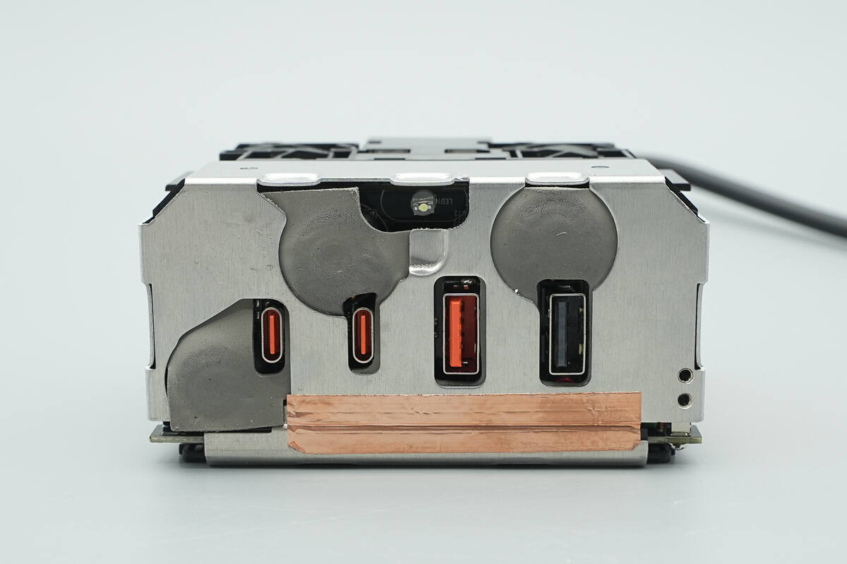
The area beneath the front metal plate is covered with copper foil, and the interior is filled with thermal pads.
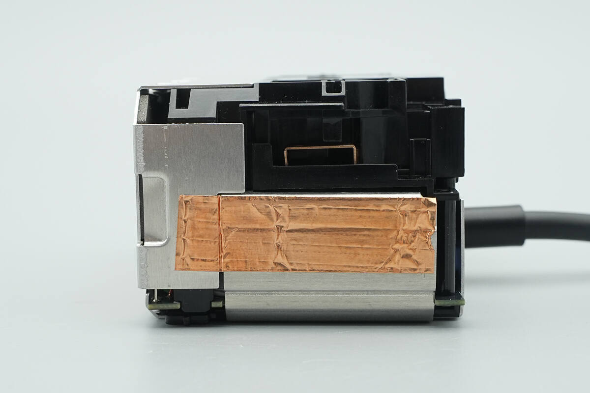
Copper foil is also applied to the metal plate on the side.
A large heat dissipation plate covers the bottom, with screws securing it at the corners.
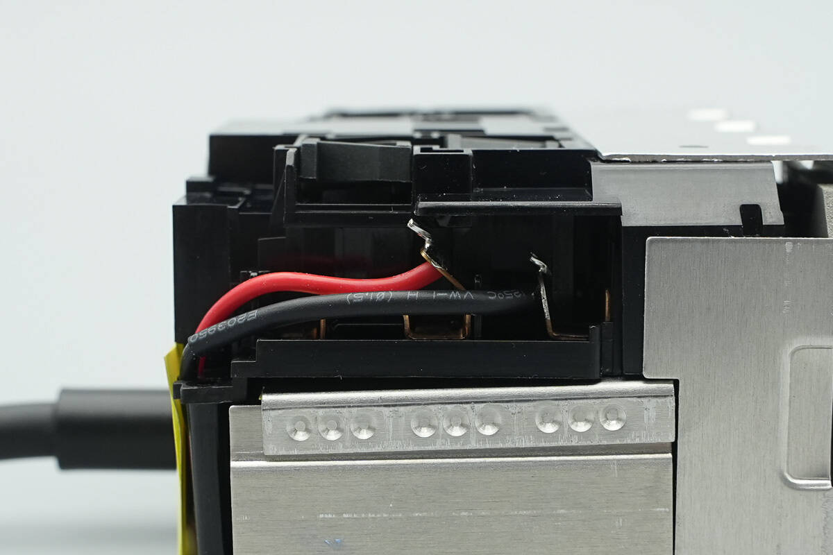
The USB fast charging module is powered through red and black wires connected to the AC socket module.
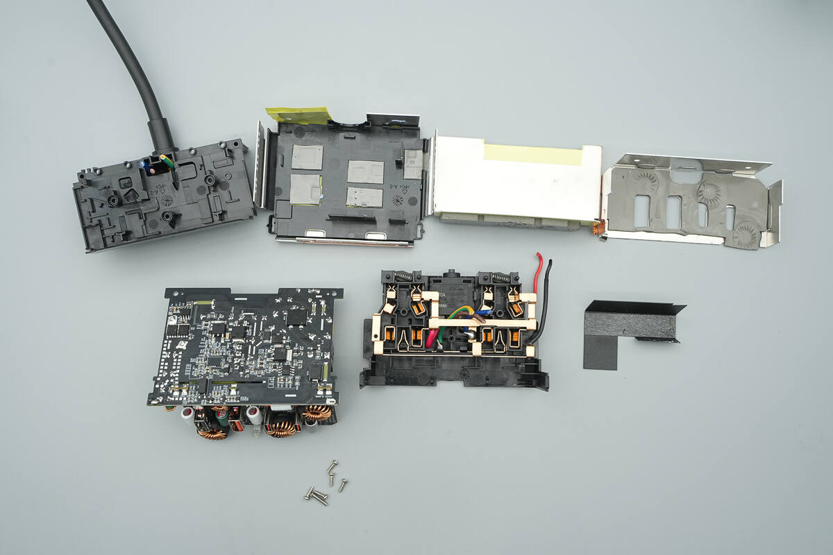
Disassemble the module.
Thermal pads are installed on the inner side of the metal heat dissipation plate.
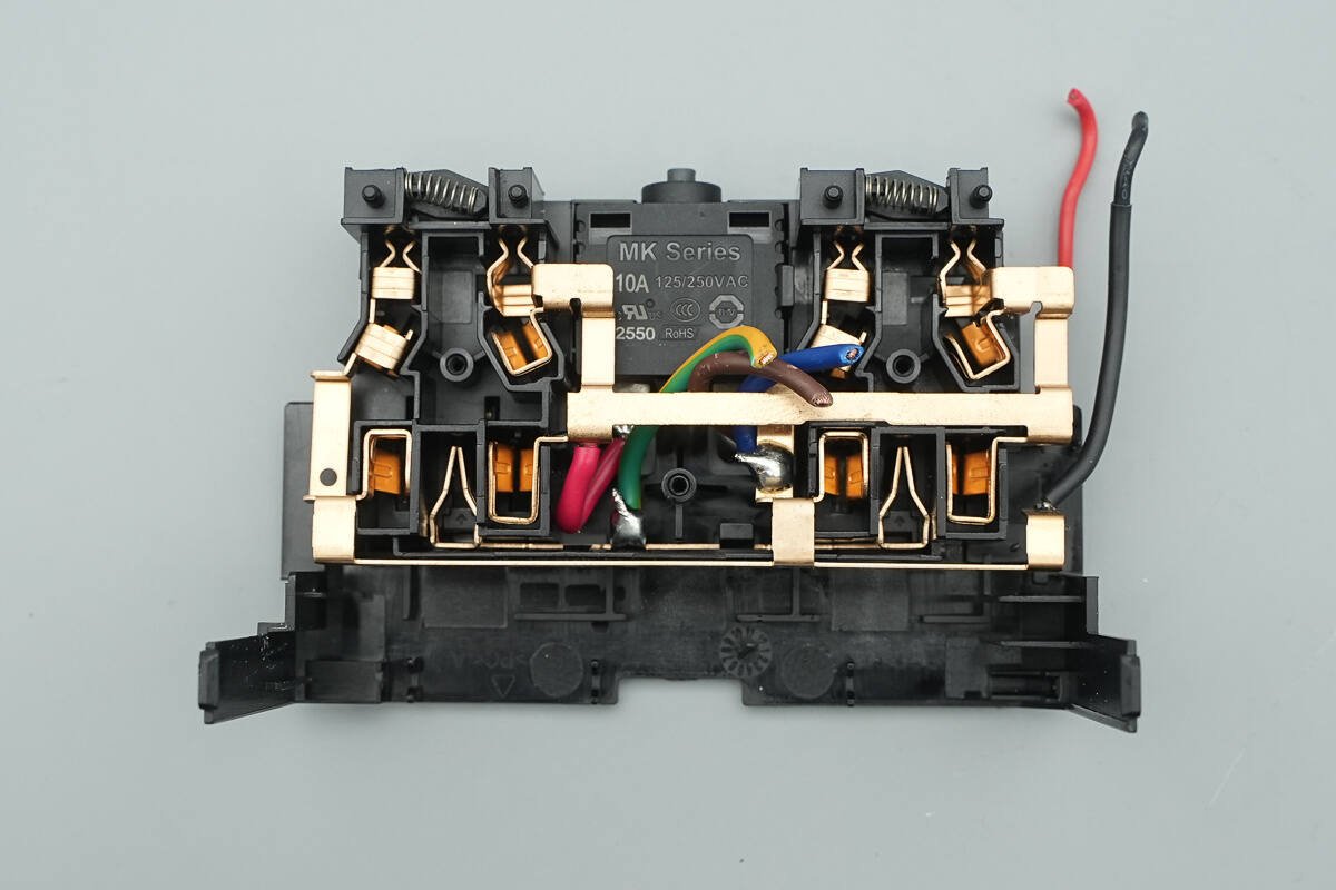
The AC socket module uses a single-piece copper strip internally.
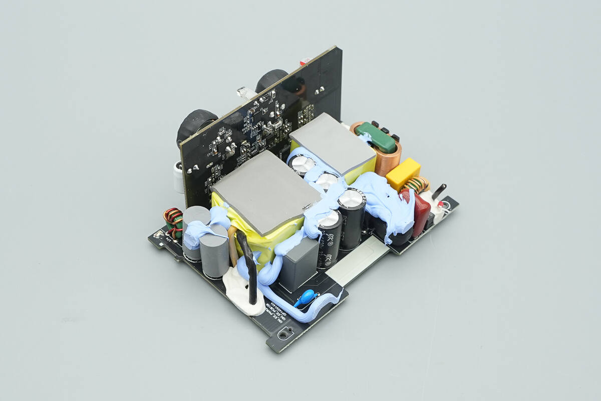
The PCBA module is composed of two PCBs welded vertically.

Disassemble and clean off the thermal adhesive and thermal pads.
The front side features components such as a time-delay fuse, common mode chokes, film capacitors, PFC boost inductor, electrolytic capacitors, a transformer, and electrolytic capacitors.
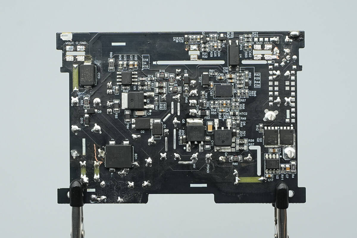
The back side features components such as a bridge rectifier, PFC boost controller, PFC MOSFET, PFC rectifier, AHB controller, AHB MOSFETs, synchronous rectifier controller, synchronous rectifiers, an optocoupler, and an SMD Y capacitor.
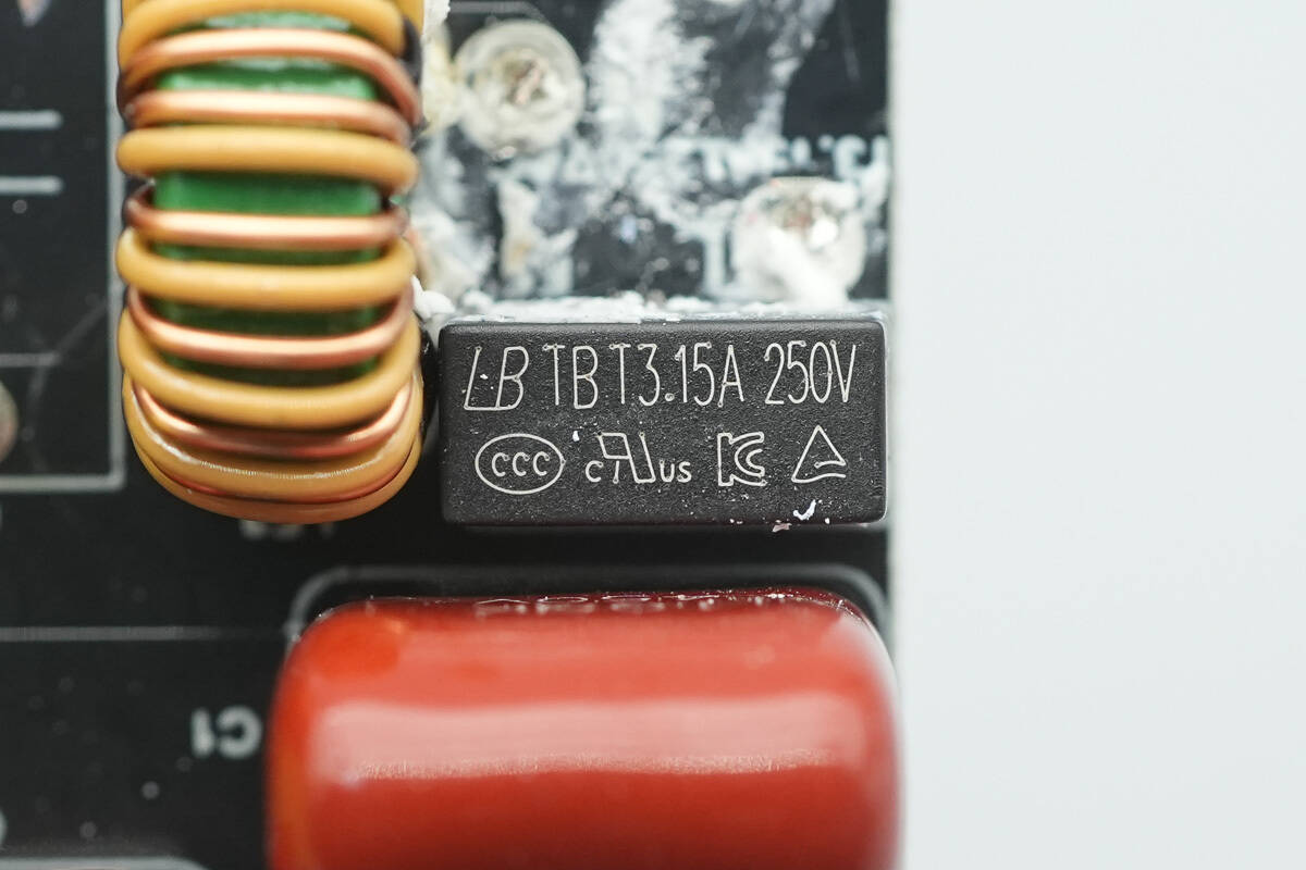
The time-delay fuse is from Lanbao, with a specification of 3.15A 250V.
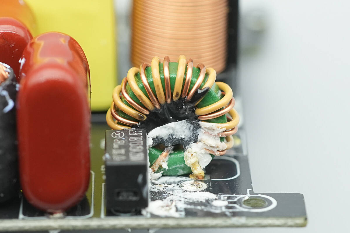
The common mode choke is wound with two wires and is used to filter out EMI.
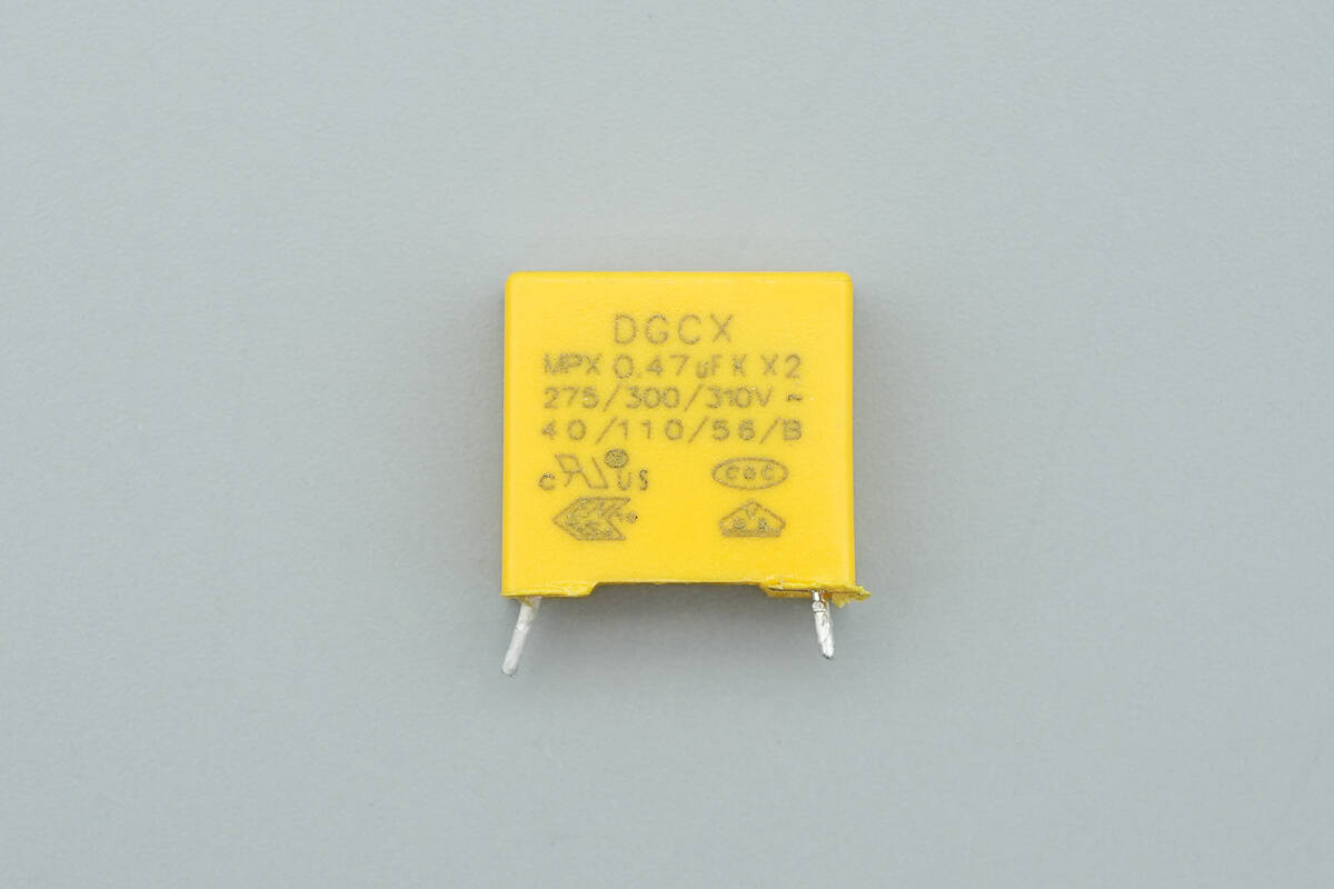
The safety X2 capacitor is from DGCX, with a capacitance of 0.47μF.
A close-up of the other common mode choke.
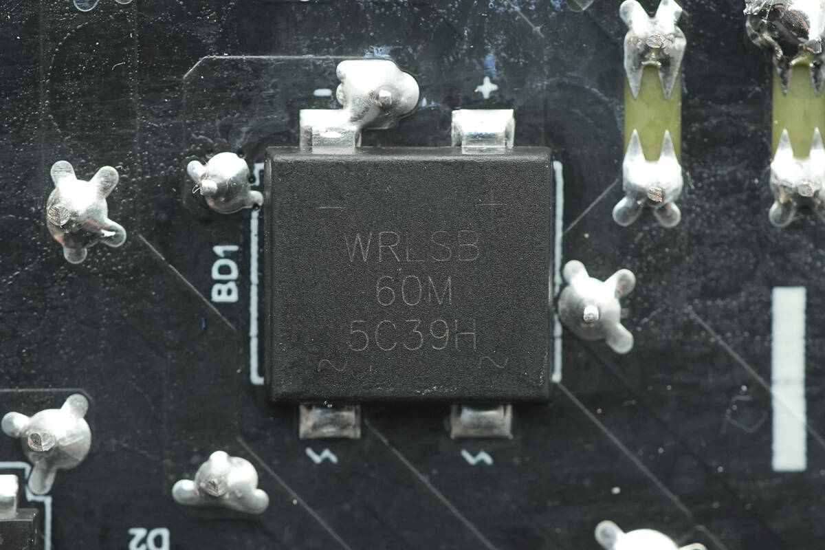
The bridge rectifier is from World Industrial, model WRLSB60M. This soft bridge rectifier, with a softer recovery curve and smoother turn-off characteristics, helps reduce diode junction capacitance, minimizing harmonic oscillation. The chosen LSB package offers excellent heat dissipation properties, enhancing the reliability of medium to high-wattage adapters.
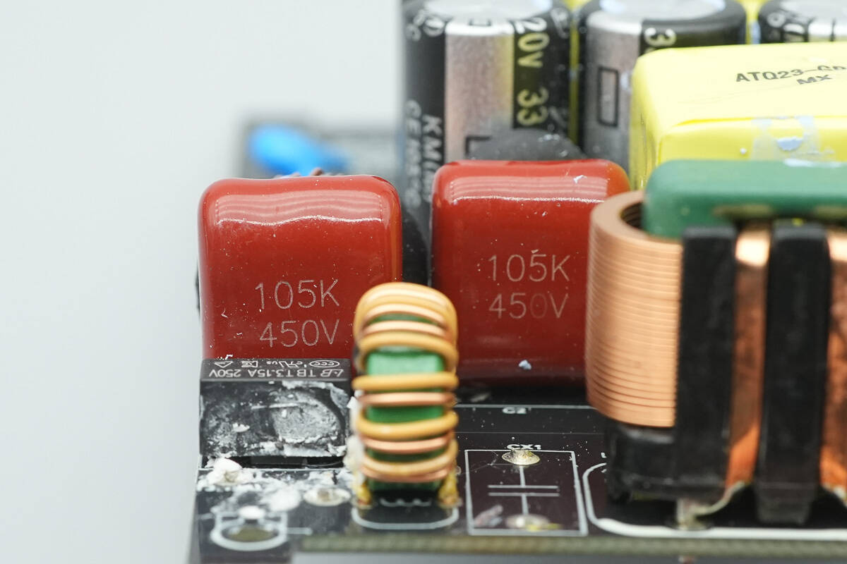
Both film capacitors have a specification of 1μF 450V.
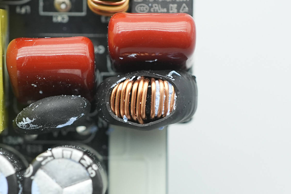
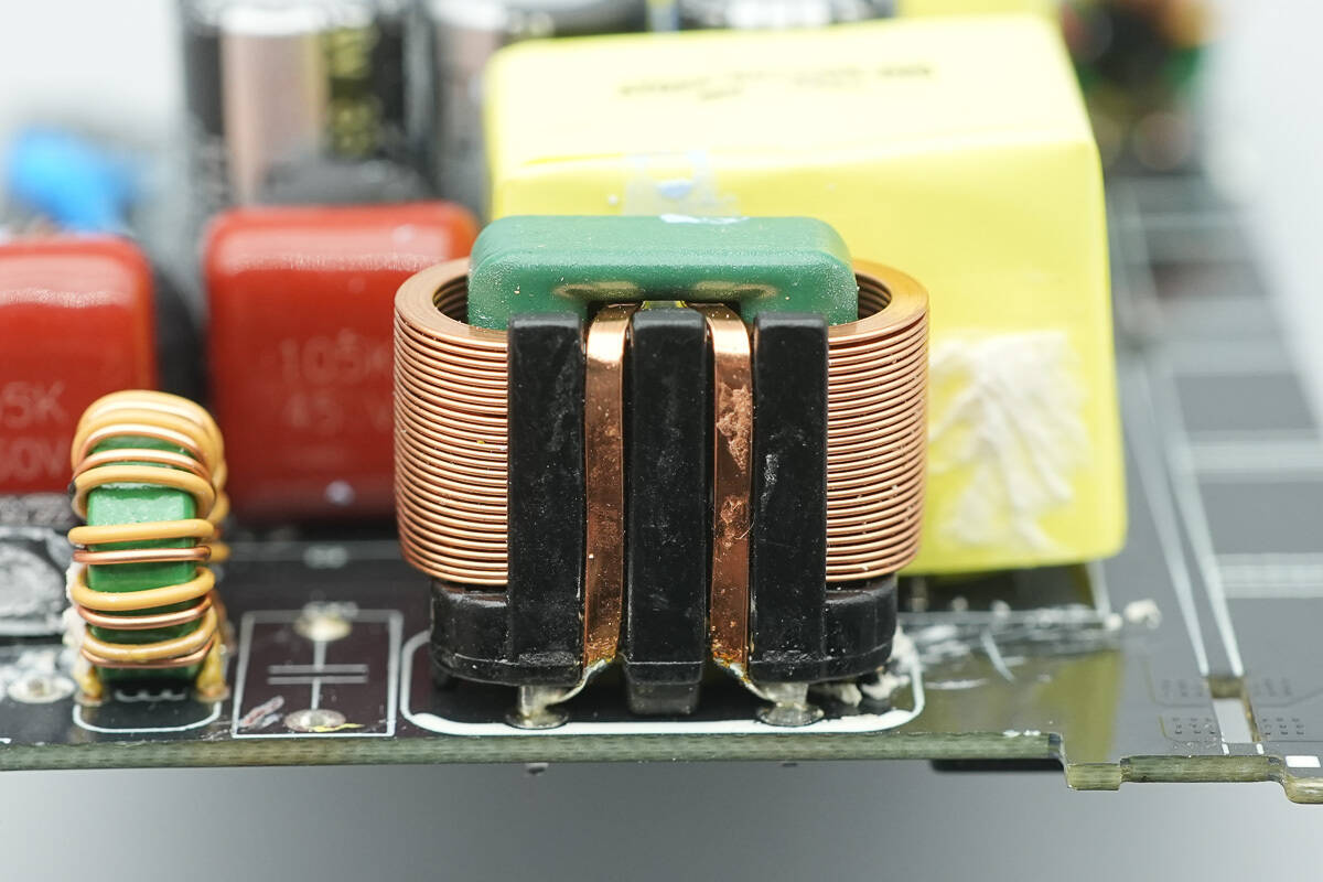
The filter inductor is insulated with heat shrink tubing.
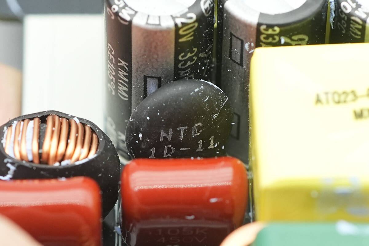
The NTC thermistor is used to suppress inrush current at power-on.
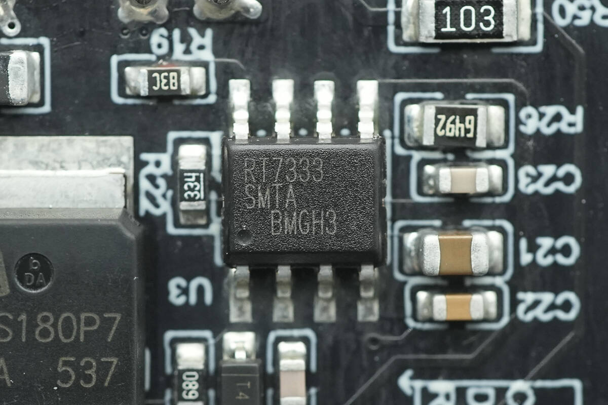
The PFC controller is from RICHTEK, model RT7333. It supports operating frequencies of up to 130kHz, 180kHz, 240kHz, and 400kHz, providing more options for different power conversion requirements. Additionally, it supports direct drive of GaN or MOSFETs, further enhancing system efficiency and simplifying the design. It comes in an SOP-8 package.
The PFC MOSFET is from Infineon, marked with 60S180P7, model IPD60R180P7S. It belongs to the CoolMOS P7 series, with a voltage rating of 650V and an Rds(on) of 180mΩ. The MOSFET is packaged in a TO252-3 package.
A close-up of the PFC boost inductor.
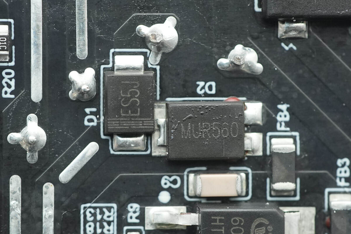
The PFC rectifier is marked with MUR560, packaged in a TO277 form factor. The bypass diode is marked with ES5J.
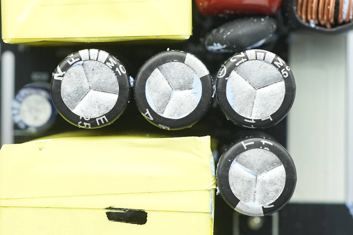
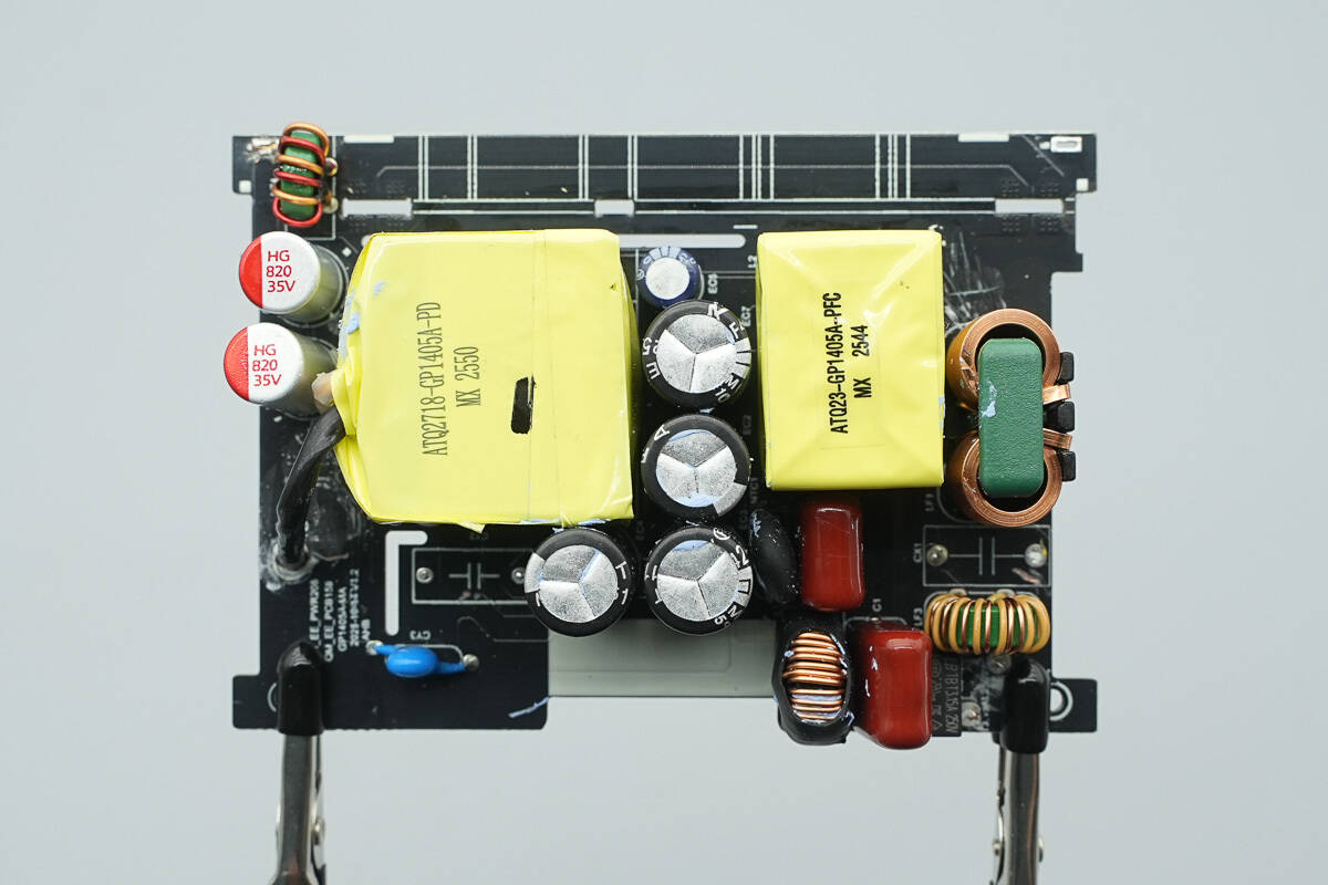
The primary side uses four electrolytic capacitors.
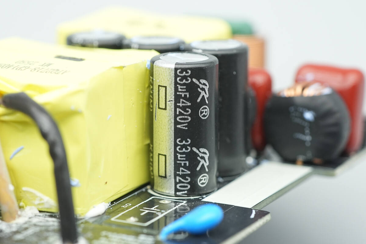
The four electrolytic capacitors are all from JK, with a specification of 420V 33μF.
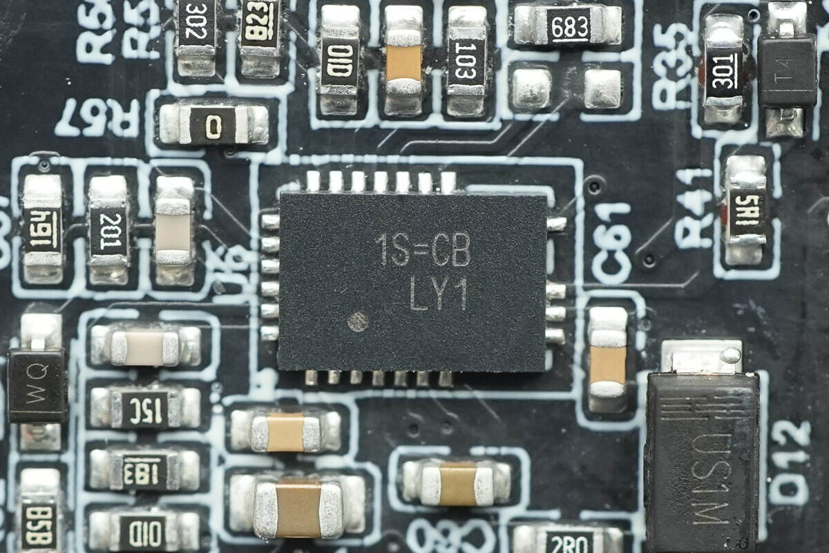
The master control chip is from RICHTEK, model RT7795M. This is a PWM controller designed specifically for Asymmetric Half-Bridge (AHB) power supplies. It features an integrated 625V high-voltage startup device and supports output power up to 300W with a voltage range of 5-48V. The RT7795M includes X-capacitor discharge and operates in continuous resonant mode, effectively reducing power loss in the secondary-side synchronous rectifiers.
The RT7795M integrates a driver that can directly drive GaN or MOSFETs, simplifying the design. The VCC supports a voltage range of 11V to 63.2V. It also allows for PFC switch control, further enhancing design flexibility and efficiency, making it suitable for various power conversion applications. The chip is packaged in a WQFN-24L form factor.
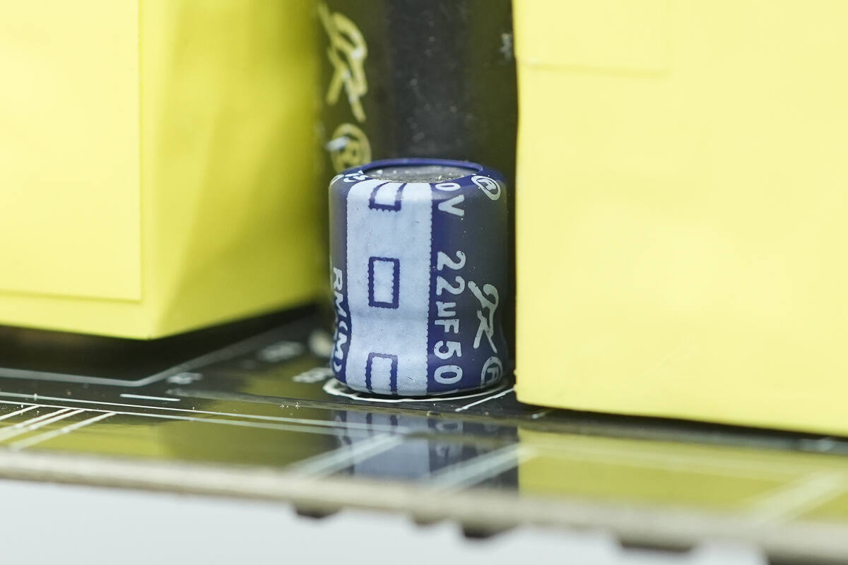
The capacitor supplying power to the master control chip is also from JK, with a specification of 50V 22μF.
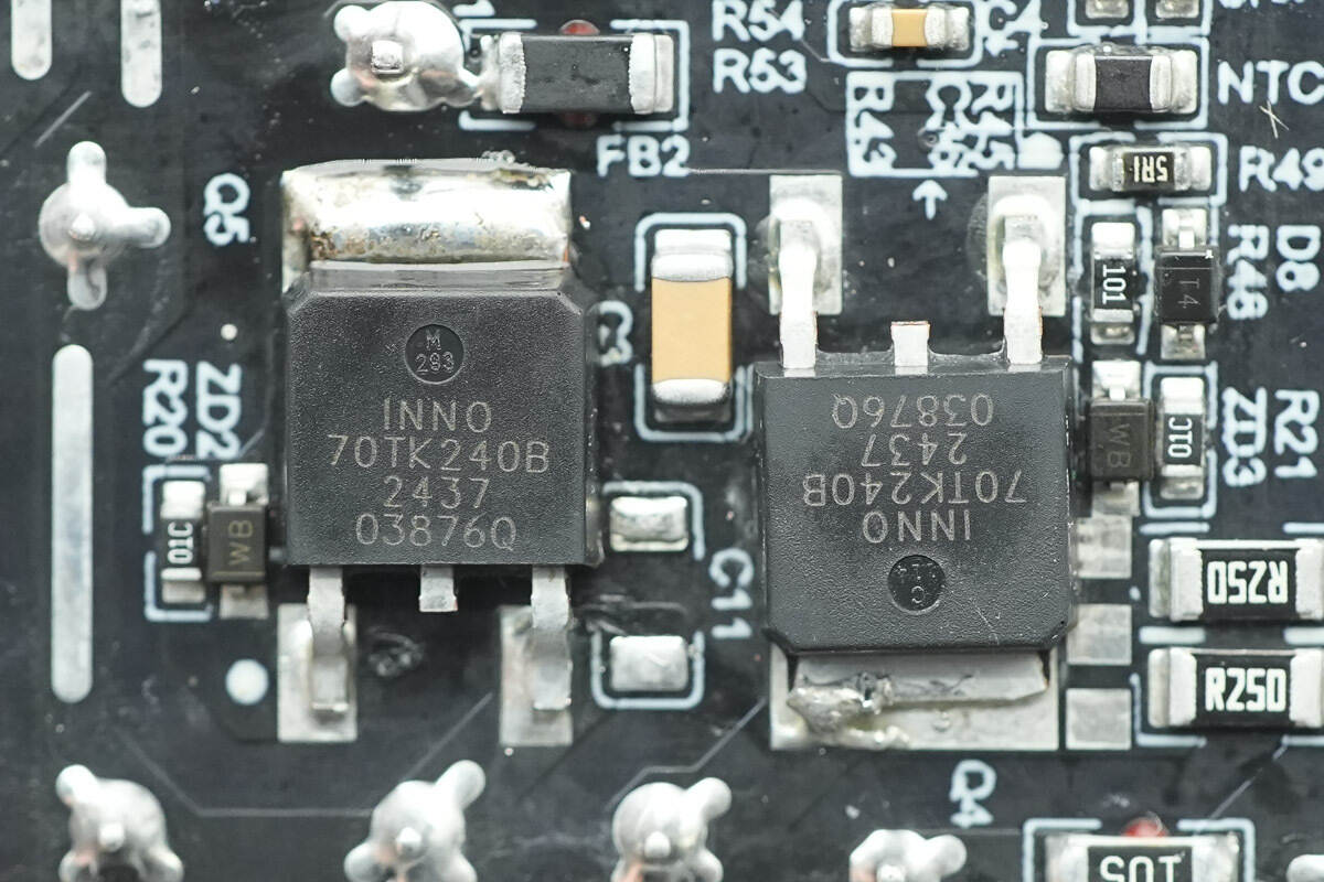
The AHB MOSFETs are from Innoscience, model INN700TK240B. This is an enhanced GaN FET with a voltage rating of 700V and a transient voltage rating of 800V. It has an Rds(on) of 240mΩ and meets the industrial application requirements according to JEDEC standards. The device also features integrated ESD protection and comes in a TO252 package.
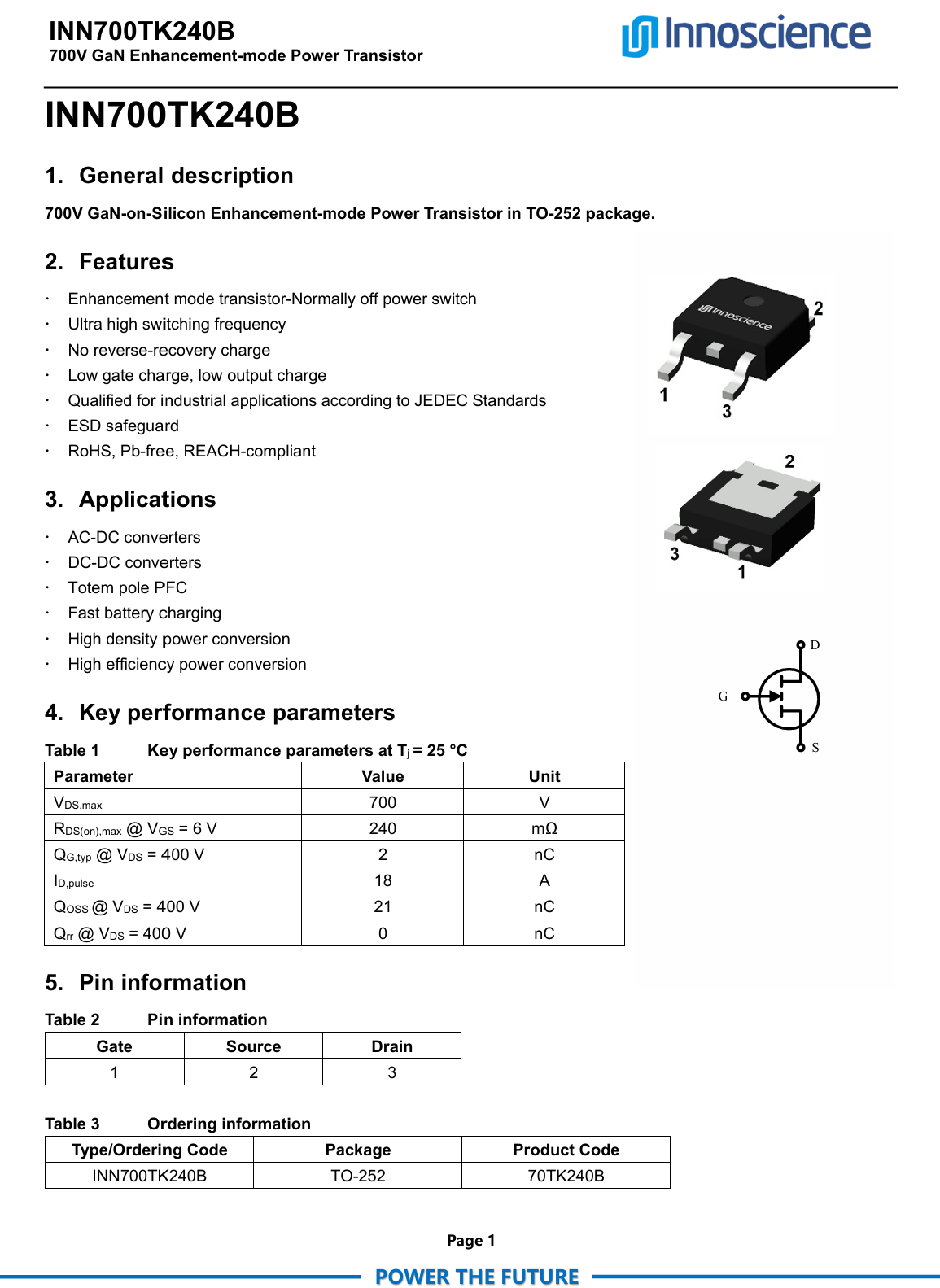
Here is the information about Innoscience INN700TK240B.
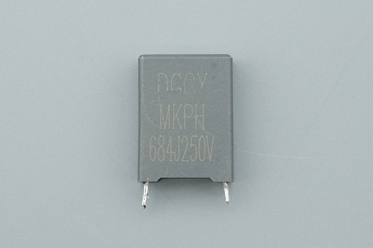
The resonant capacitor is from DGCX, with a specification of 0.68μF 250V.
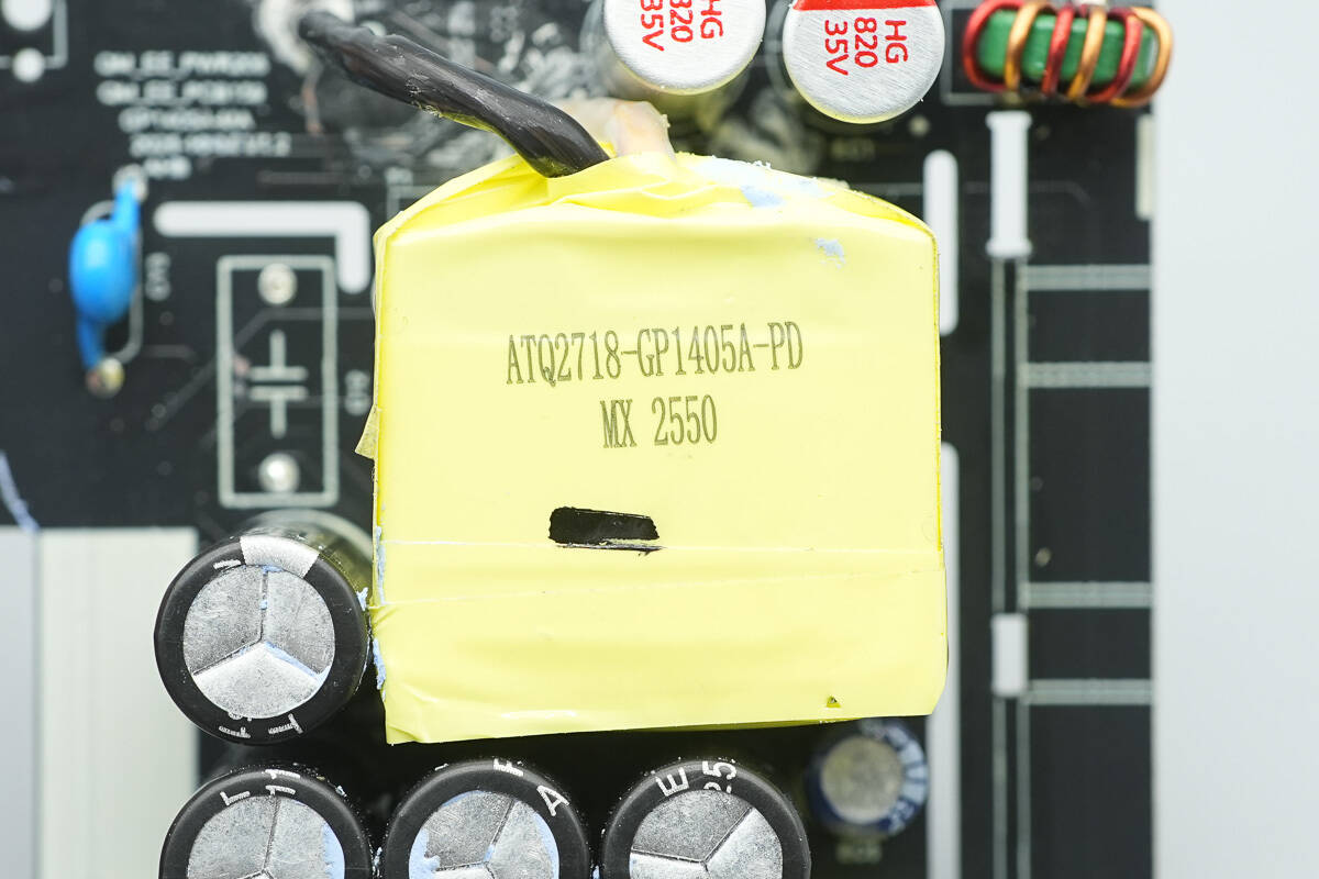
A close-up of the transformer.
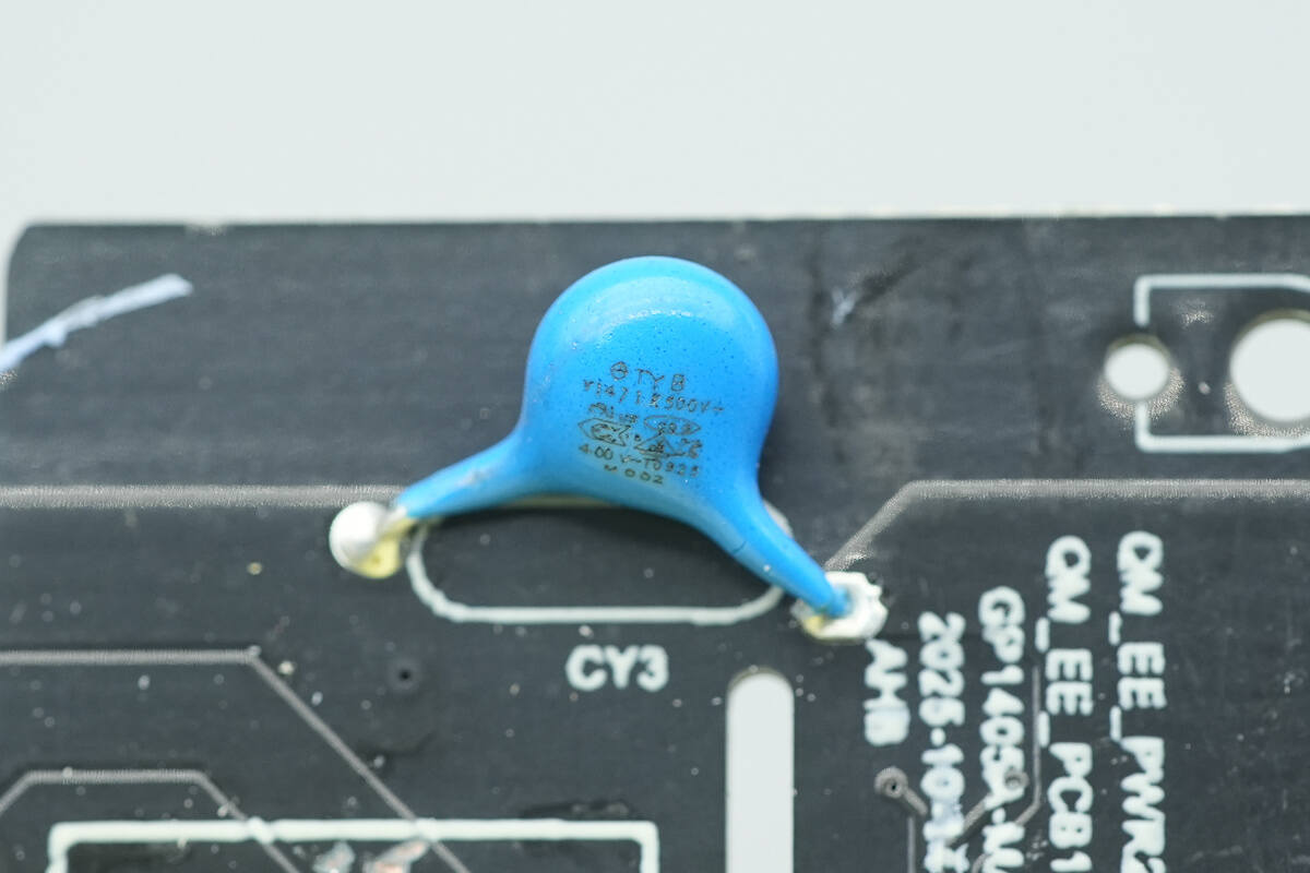
A close-up of the blue Y capacitor.
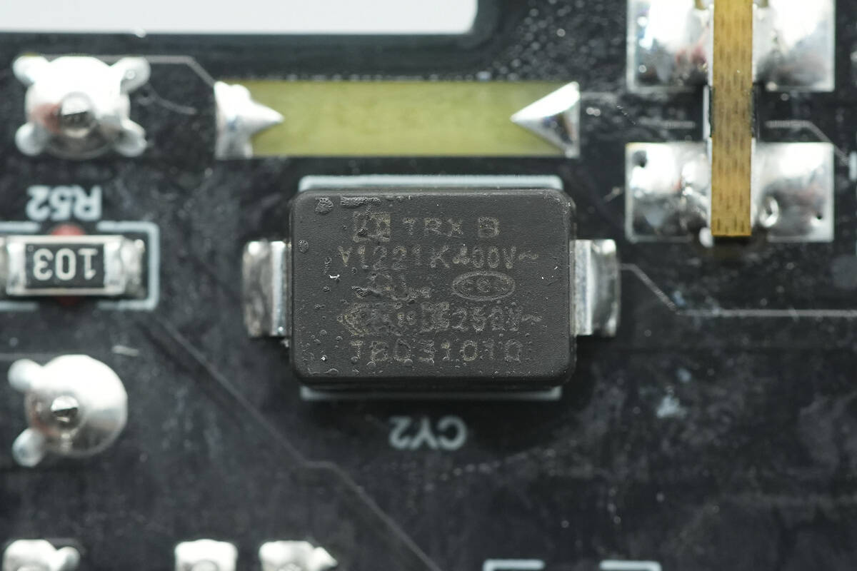
The SMD Y capacitor is from TRX, with part number TMY1221K. Its compact size and lightweight design make it ideal for high-density power products such as GaN fast chargers.
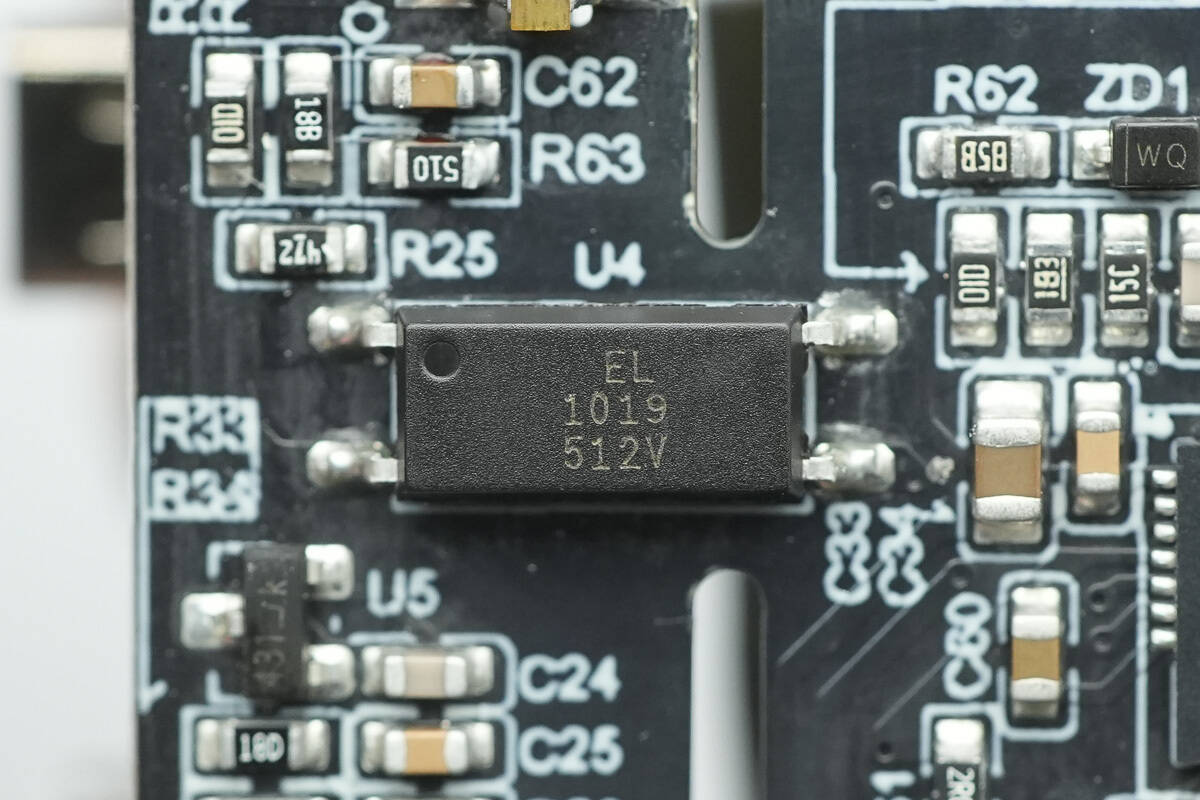
The Everlight EL1019 optocoupler is used for output voltage feedback.
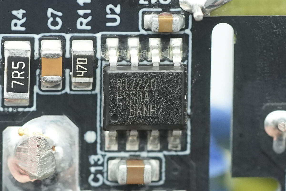
The synchronous rectifier controller is from RICHTEK, model RT7220E. It supports Asymmetric Half-Bridge (AHB) conversion and works in CRM/CSM/BM modes. The RT7220E controls the SR gate switching state by detecting the drain voltage of the MOSFET. This feature minimizes the turn-off dead time and transmits sine-wave energy through SR gate pulses, improving overall efficiency.
The RT7220E supports a wide output voltage range of 5-48V and includes an integrated high-to-low differential linear voltage regulator, specifically designed to power the MOSFET gate driver at low output voltages. When used in conjunction with the RT7795 AHB controller, the RT7220E enables a dual-pulse function to optimize efficiency under heavy load or low output voltage conditions. It is packaged in an SOP-8 form factor.

The synchronous rectifiers are from JJWD, model JMSL1006PG. They are NMOS transistors with a voltage rating of 100V and a Rds(on) of 4.3mΩ. The transistors are packaged in a PDFN 5x6-8L form factor.
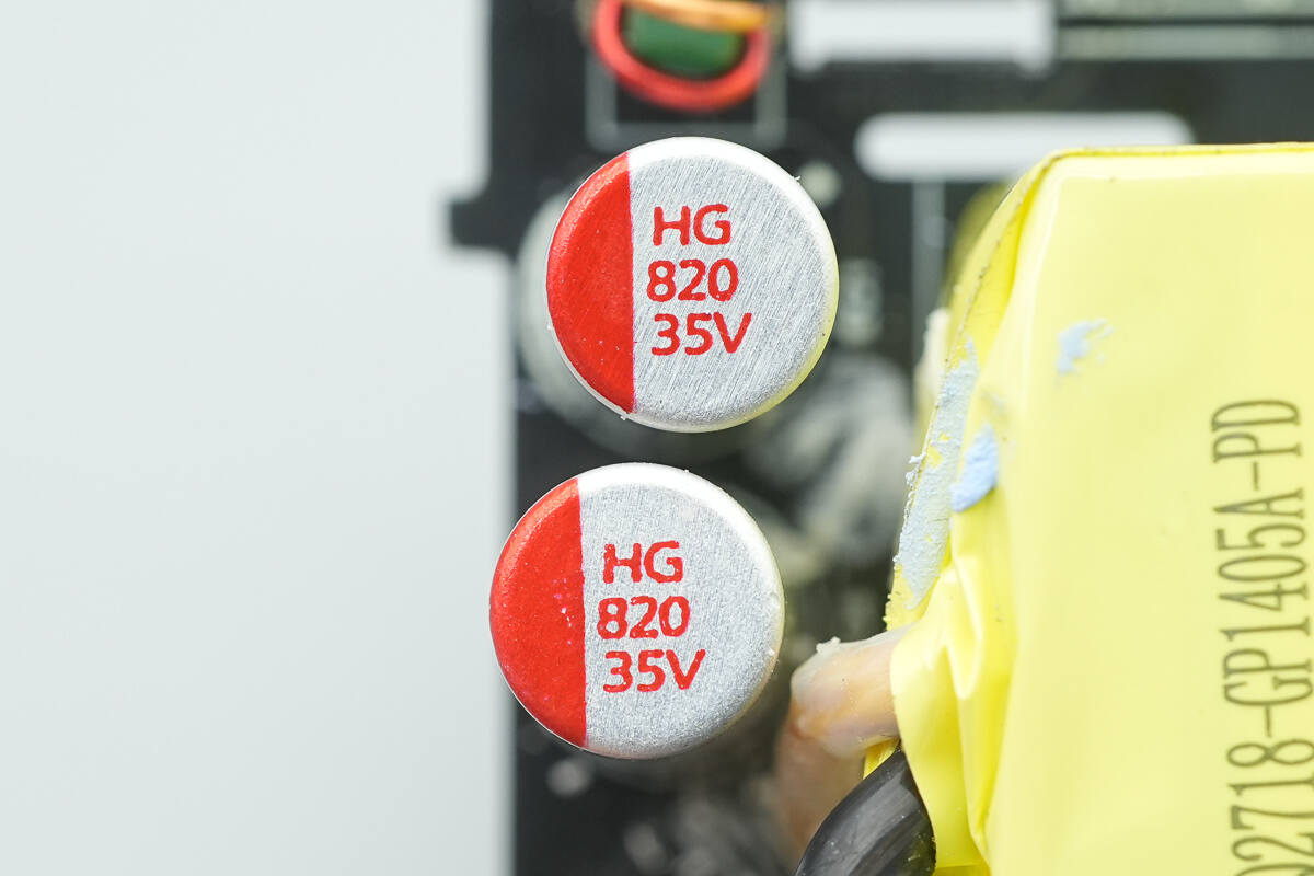
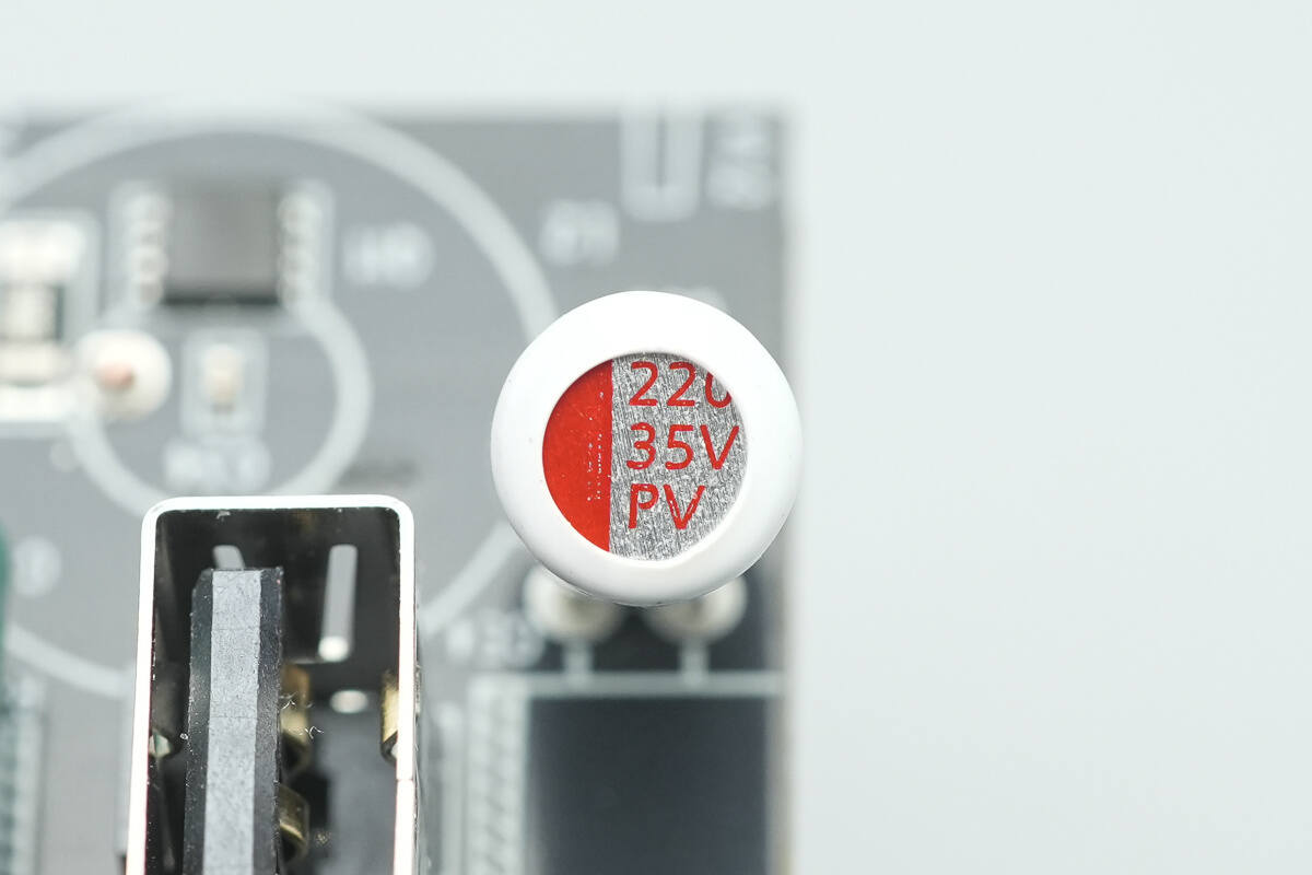
The two output filter electrolytic capacitors have a specification of 35V 820μF.
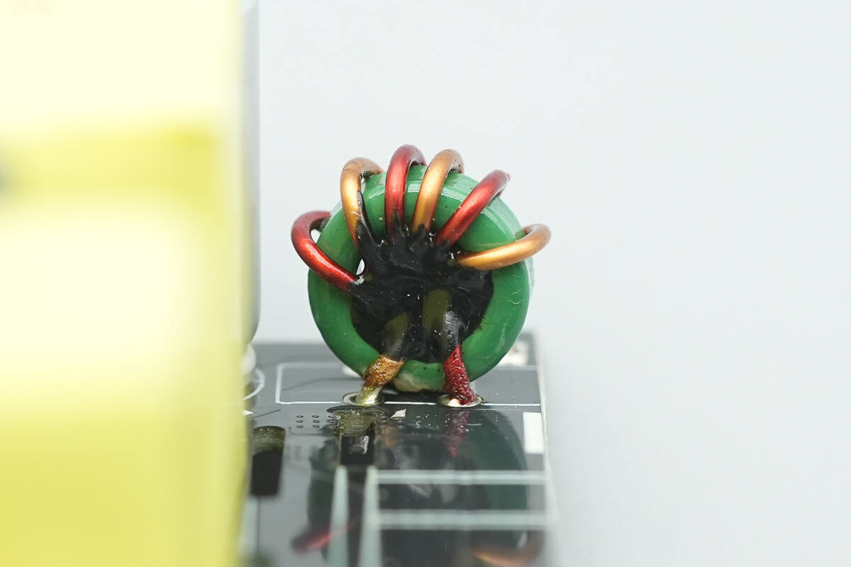
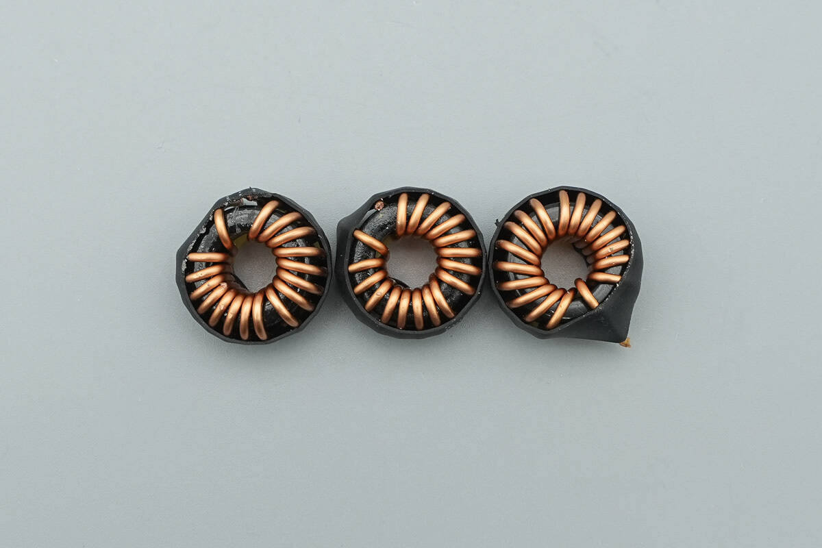
A close-up of the filter inductor.
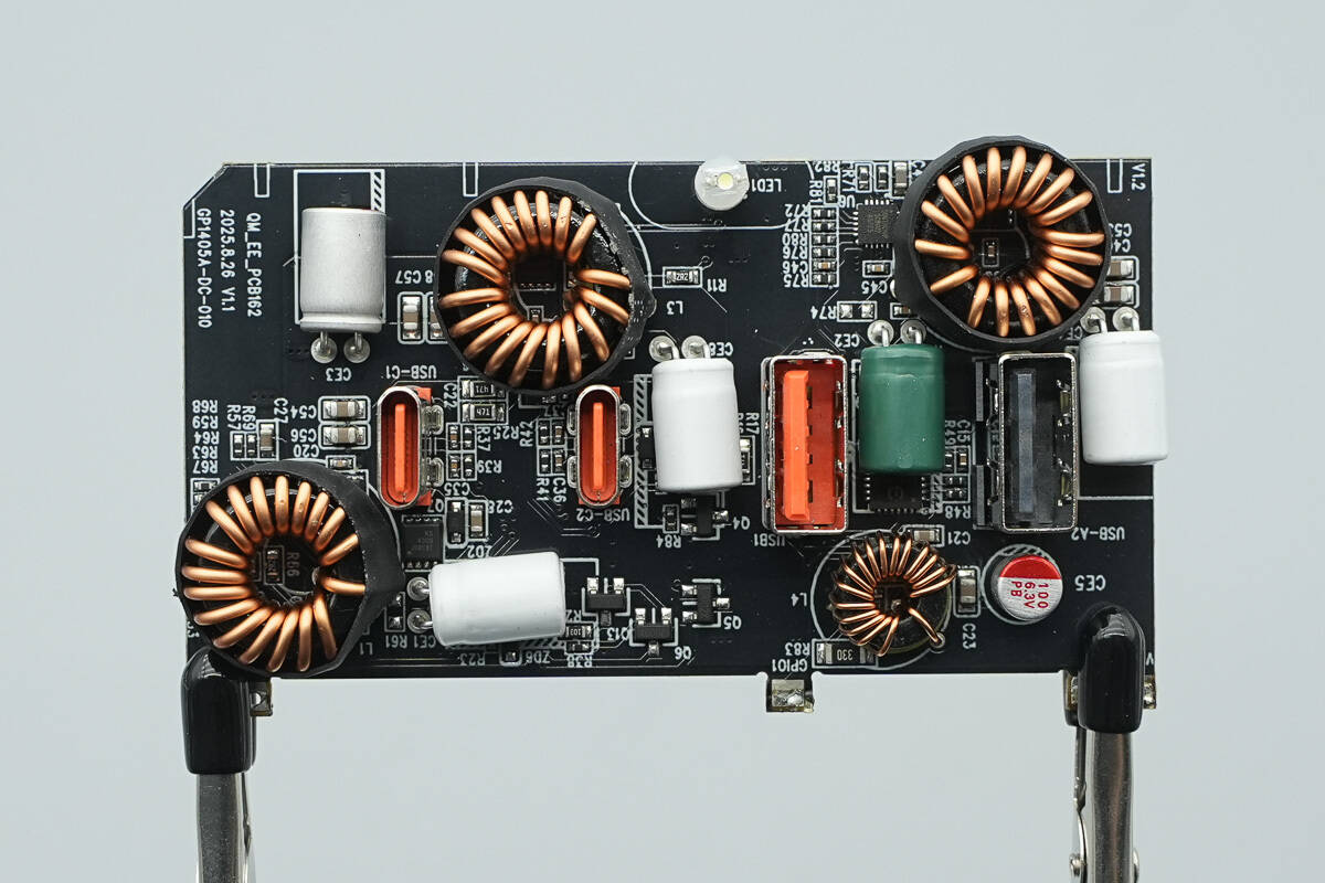
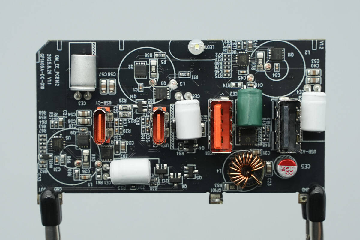
The front of the small PCB at the output terminal is equipped with an indicator light, a buck inductor, and secondary buck output filter electrolytic capacitors, among other components.
After removing the inductors, you can see components such as synchronous buck controllers, synchronous buck MOSFETs, protocol chip, and output VBUS MOSFETs.
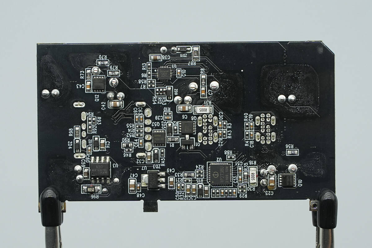
The back side features components such as a synchronous buck controller, synchronous buck converter, synchronous buck MOSFETs, protocol chip, and a VBUS MOSFET.
A close-up of the indicator light.

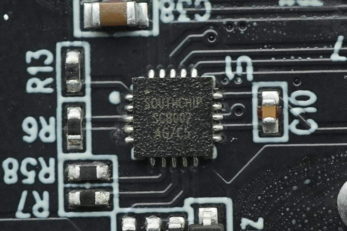
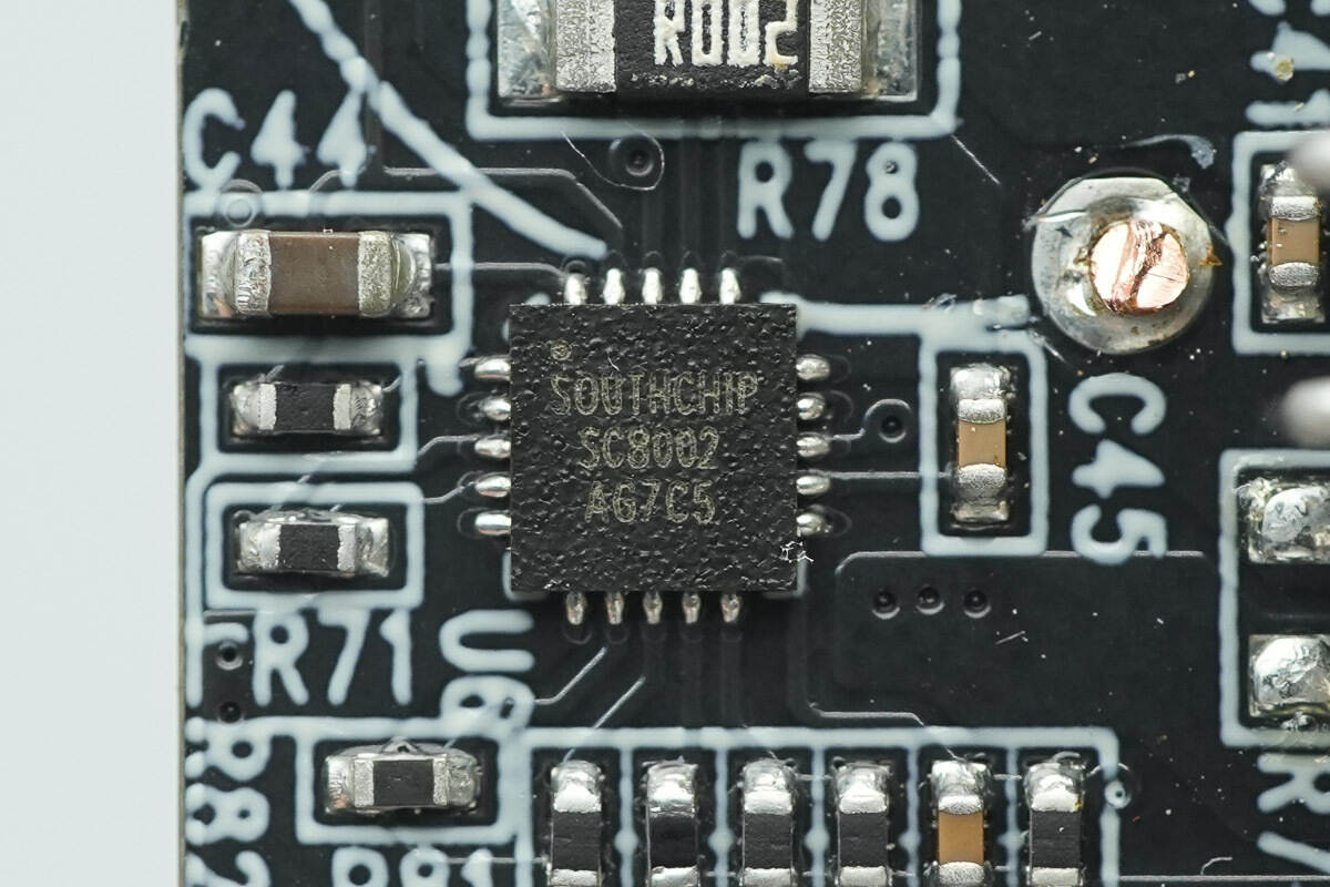
The synchronous buck controller used for the USB-C1 port is from SouthChip, model SC8002. It supports an input voltage range of 4.6-36V, with adjustable output voltage and a fixed 5V output for fast charging applications. The chip features high-precision output current limiting, supports dual-channel independent current limiting, and integrates comprehensive protection functions. The SC8002 is packaged in a QFN 3x3-20 form factor, making it suitable for applications such as car chargers, multi-port chargers, and USB hubs.

Here is the information about SouthChip SC8002.
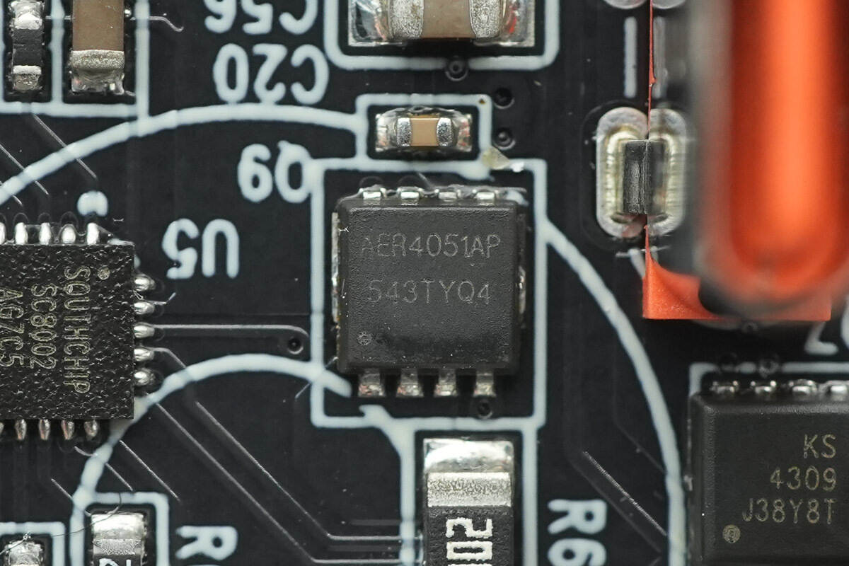
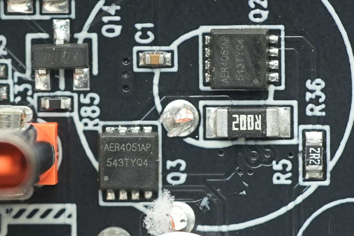
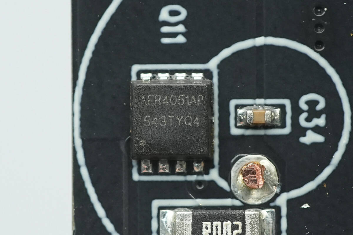
The two synchronous buck MOSFETs used in conjunction with the SC8002 are from ALLEPIC, model AER4051AP. These are NMOS transistors with a voltage rating of 40V and an Rds(on) of 5.5mΩ. The MOSFETs are packaged in a PDFN 3030 form factor.
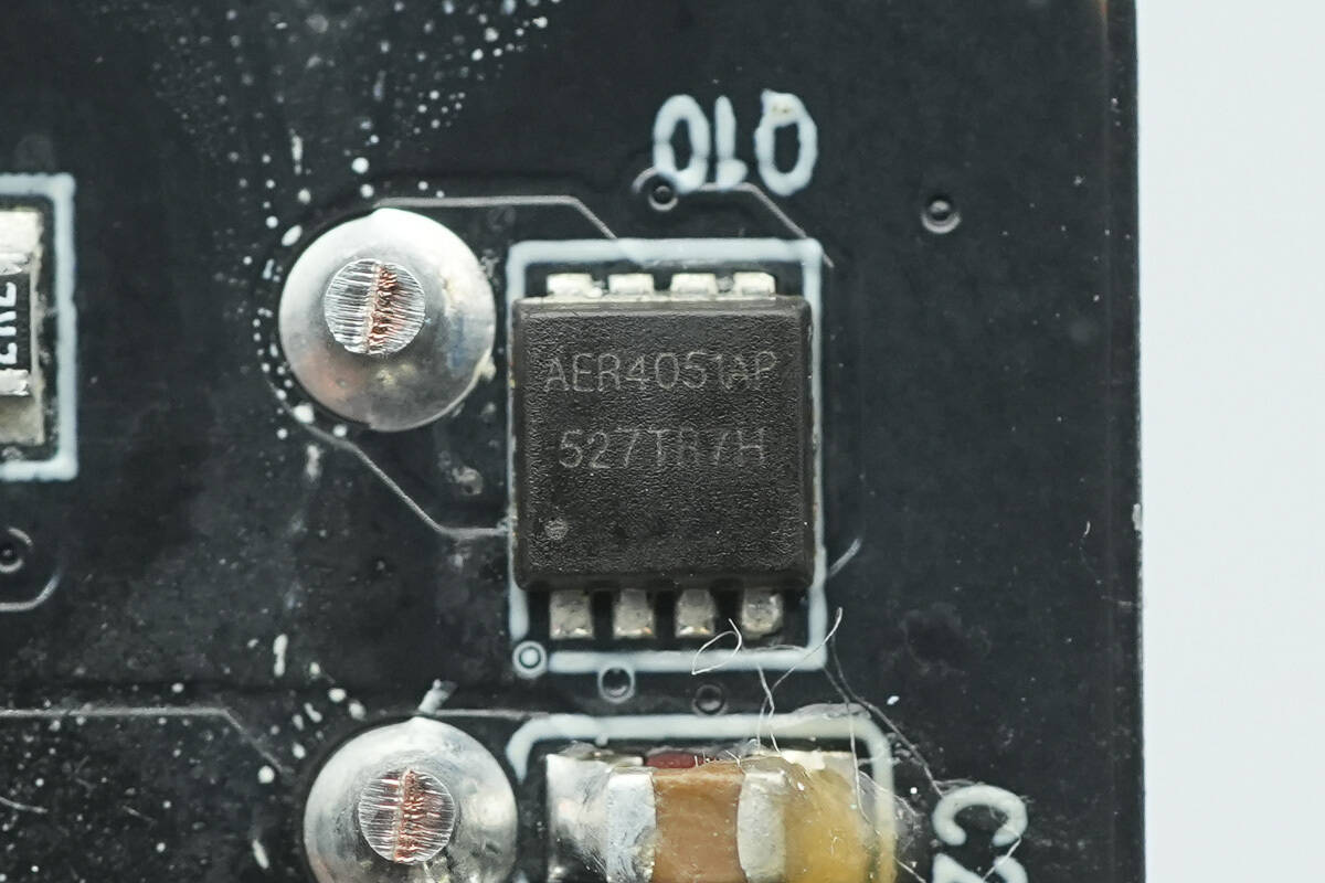
The other ALLEPIC AER4051AP synchronous buck MOSFET is located on the opposite side.
The synchronous buck controller used for the USB-C2 port is also the SouthChip SC8002.
The two synchronous buck MOSFETs used for the USB-C2 port are also ALLEPIC AER4051AP.
The synchronous buck controller used for the USB-A1 port is also the SouthChip SC8002.
The two synchronous buck MOSFETs used for the USB-A1 port are also ALLEPIC AER4051AP.
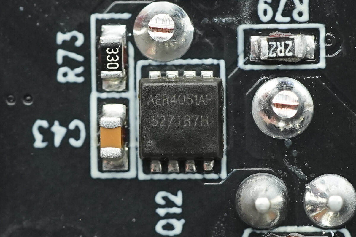
The other ALLEPIC AER4051AP synchronous buck MOSFET is located on the opposite side.
The inductors in the three buck converter circuits are all insulated with heat shrink tubing.
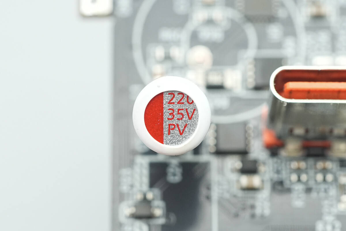
The secondary buck output filter electrolytic capacitor is insulated with a plastic sleeve, with a specification of 35V 220μF.
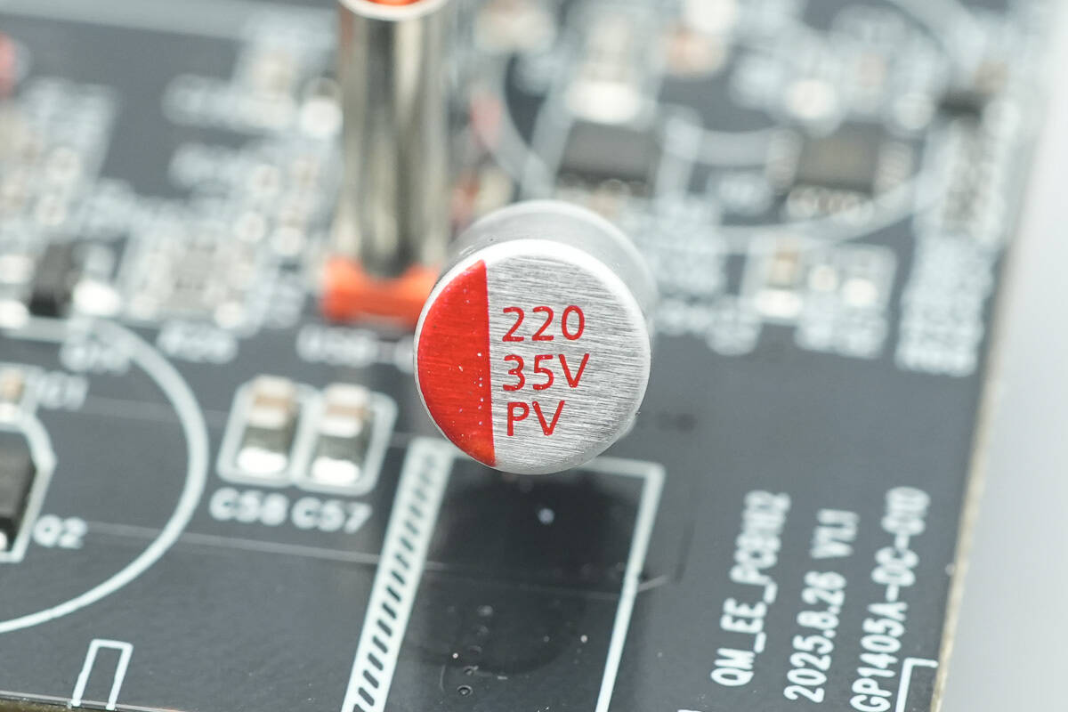
The second electrolytic capacitor also has a specification of 35V 220μF.
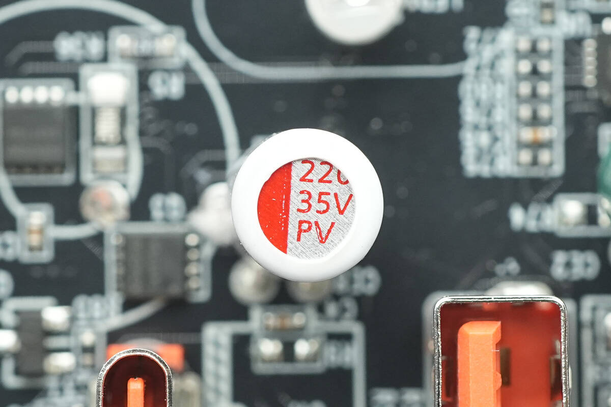
The third electrolytic capacitor has the same specification of 35V 220μF.
The fourth electrolytic capacitor also has the same specification of 35V 220μF.
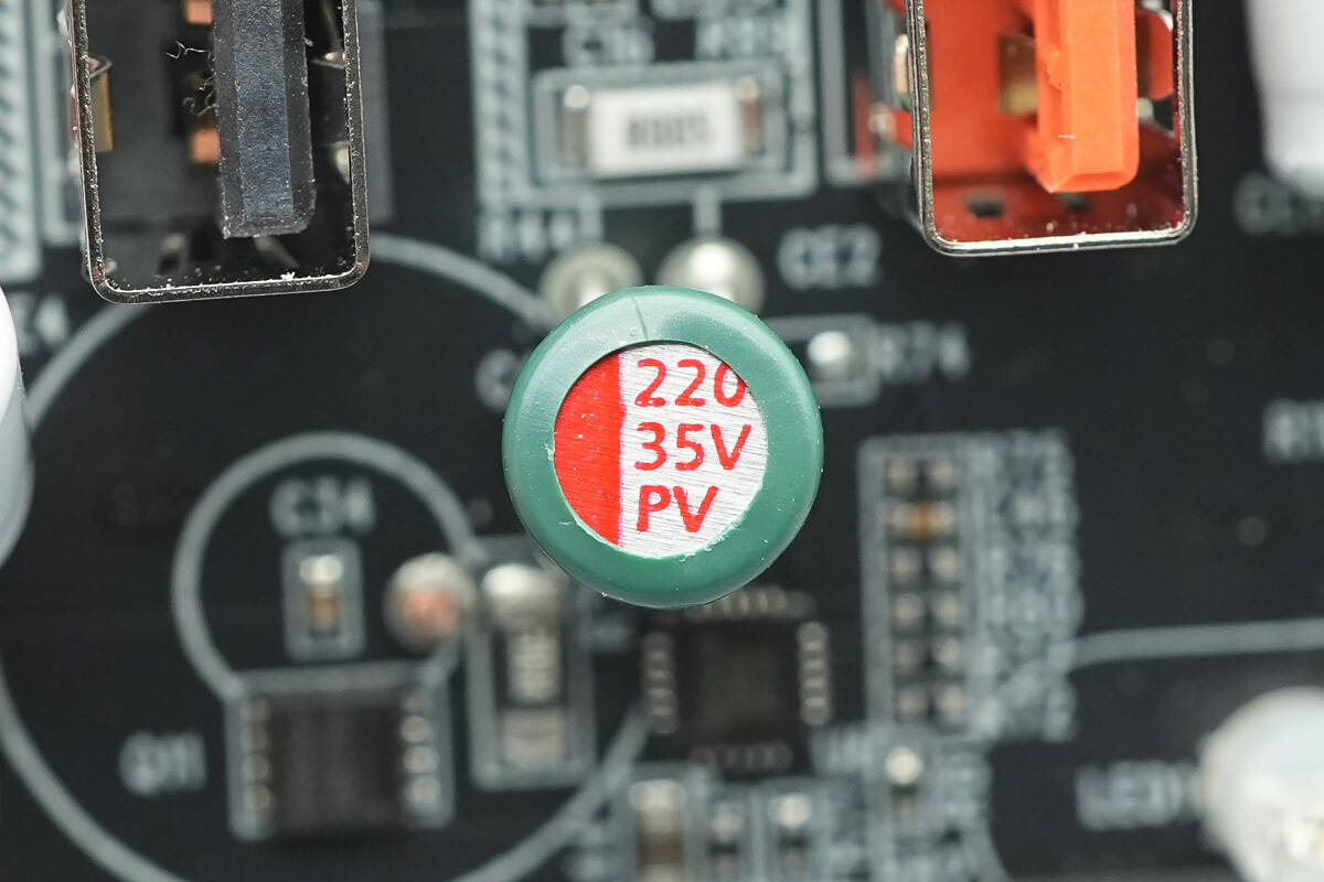
The fifth electrolytic capacitor also has the same specification of 35V 220μF.
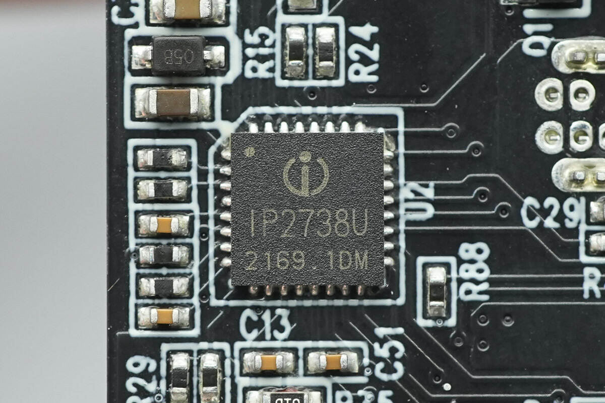
The USB-C protocol chip is from Injoinic, model IP2738U. This chip supports multiple USB ports and is designed for dual-port 18-140W fast charging applications. It features independent feedback control and USB PD control, essentially integrating two IP2736 chips into a single chip. The fast charging specifications are the same as those of the IP2736. It supports USBPD 3.1, 28V EPR, UFCS, and a wide range of fast charging protocols such as PD3.0/PPS, ensuring excellent compatibility.
The Injoinic IP2738U includes four independent NMOS drivers, which can control multiple output ports. It controls multiple VBUS MOSFETs for output port switching and parallel power control. Additionally, it supports dual independent overcurrent, overvoltage, and short-circuit protection, ensuring safe usage.
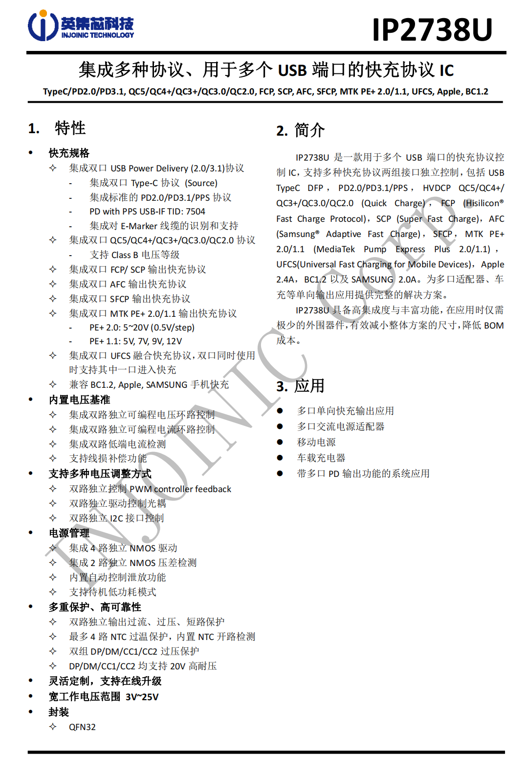
Here is the information about Injoinic IP2738U.
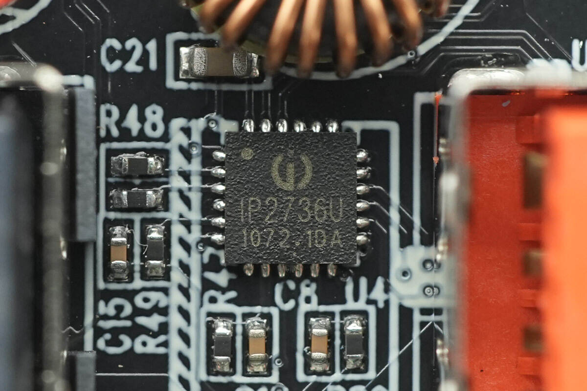
The USB-A1 protocol chip is from Injoinic, model IP2736U. This chip integrates multiple protocols and is designed for fast charging protocol control in USB ports. The IP2736U supports a wide range of fast charging protocols, including USB Type-C DP, PD2.0/PD3.1/PPS/EPR28V, HVDCP QC5/4+/3+/3.0/2.0, FCP, SCP, AFC, SFCP, MTKPE+2.0/1.1, UFCS, Apple 2.4A, BC1.2, and SAMSUNG 2.0A. It provides a complete solution for adapters, car chargers, and other single-output applications.
The Injoinic IP2736U features high integration and a rich set of functions, requiring minimal external components during application. This effectively reduces the overall solution size and lowers BOM costs.
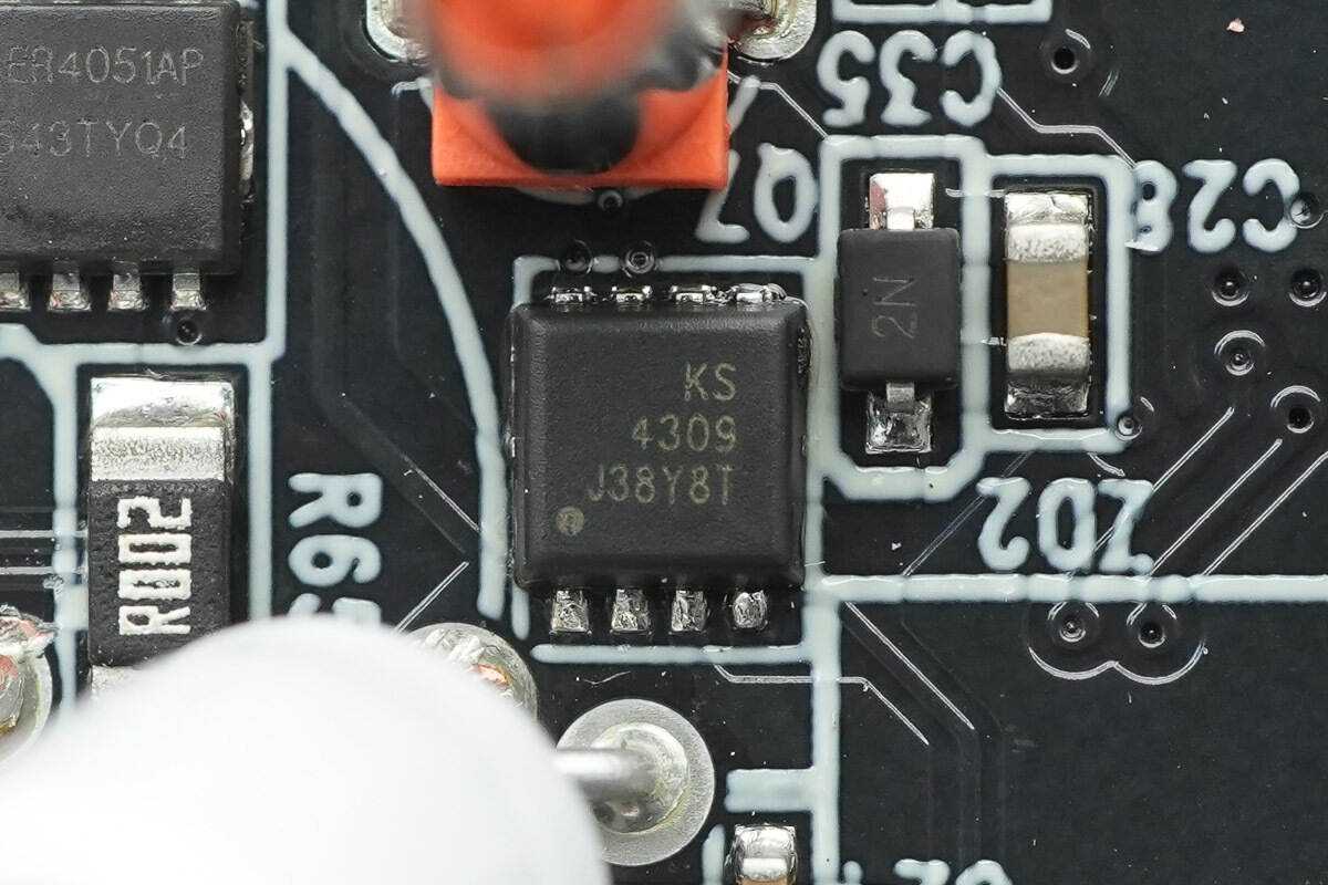
The output VBUS MOSFET for the USB-C1 port is from Kwansemi, model KS4309MA. It is a PMOS transistor with a voltage rating of -40V and a Rds(on) of 10mΩ. The MOSFET is packaged in a PDFN 3333 form factor.
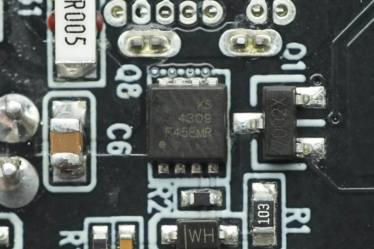
The output VBUS MOSFET for the USB-C2 port also uses the Kwansemi KS4309MA.
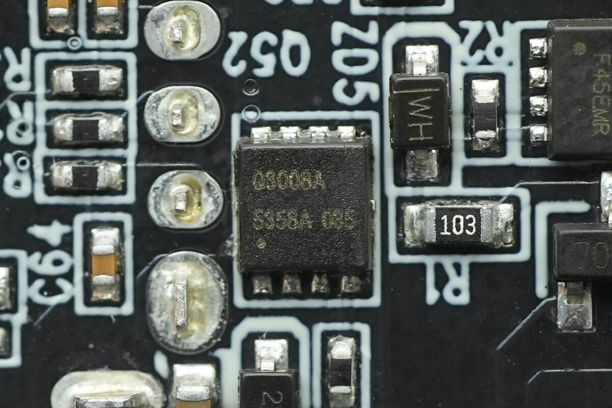
The output VBUS MOSFET for the USB-A1 port is marked with Q3008A and is packaged in a PDFN 3x3 form factor.
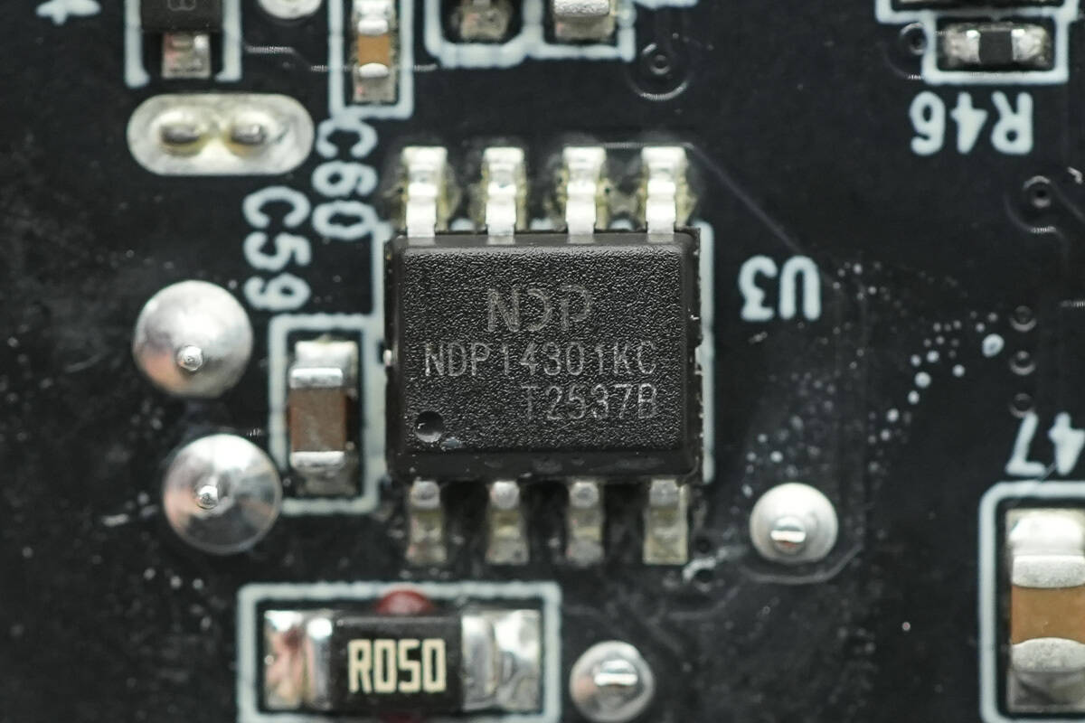
The synchronous buck converter used for the USB-A2 port is from NDP, model NDP14301KC. This is a high-efficiency, integrated synchronous buck DC/DC converter that uses a fixed-frequency average current mode control architecture. The device is capable of providing up to 3.0A of continuous load current and offers excellent line and load regulation performance. The chip requires very few external components and is equipped with a comprehensive set of protection features to ensure stable and reliable operation.
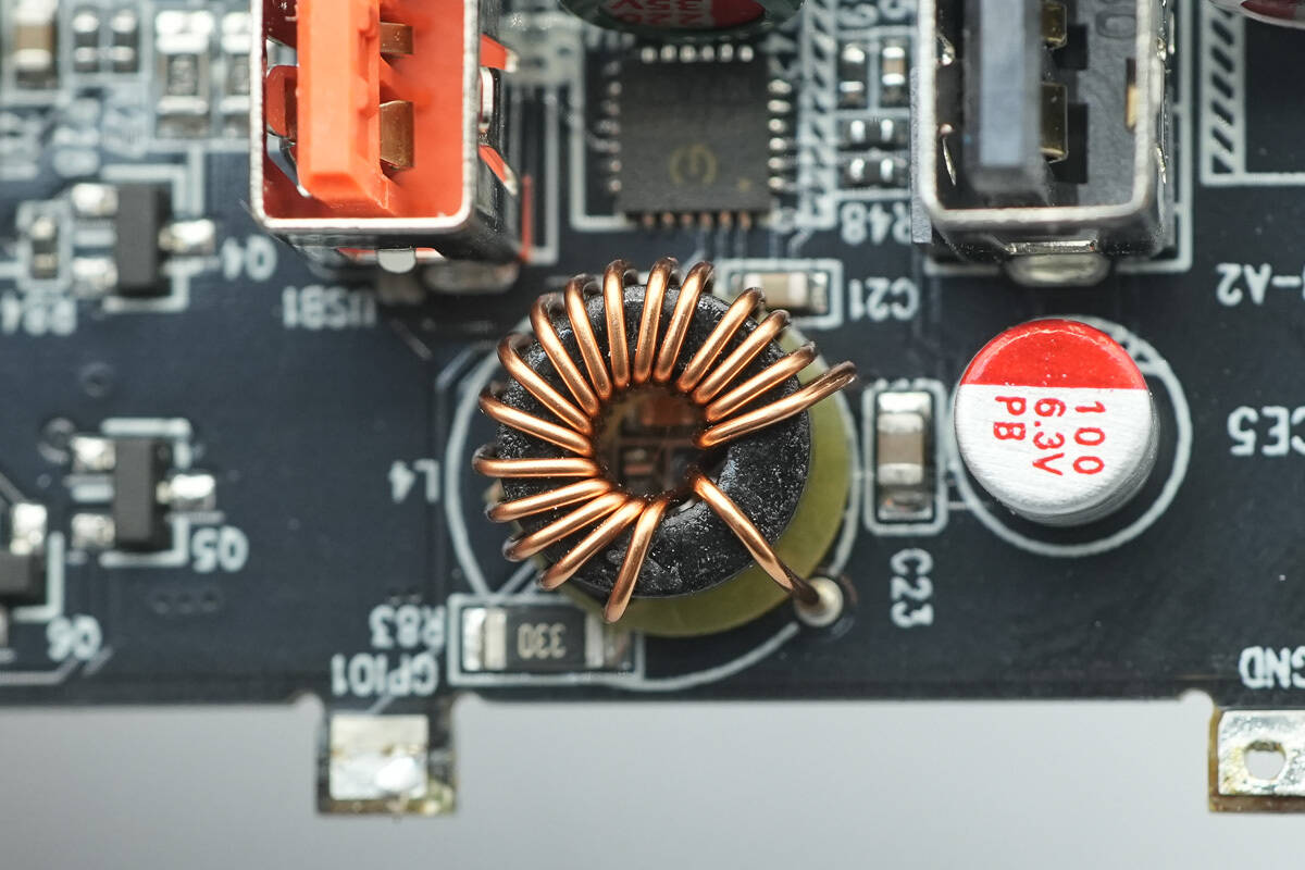
The paired buck inductor has a bakelite plate attached to its bottom.
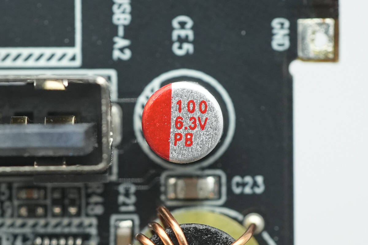
The buck output filter electrolytic capacitor has a specification of 6.3V 100μF.
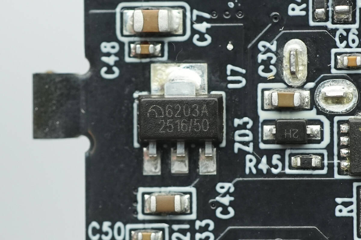
The voltage regulator chip marked with 6203A is from Microne.
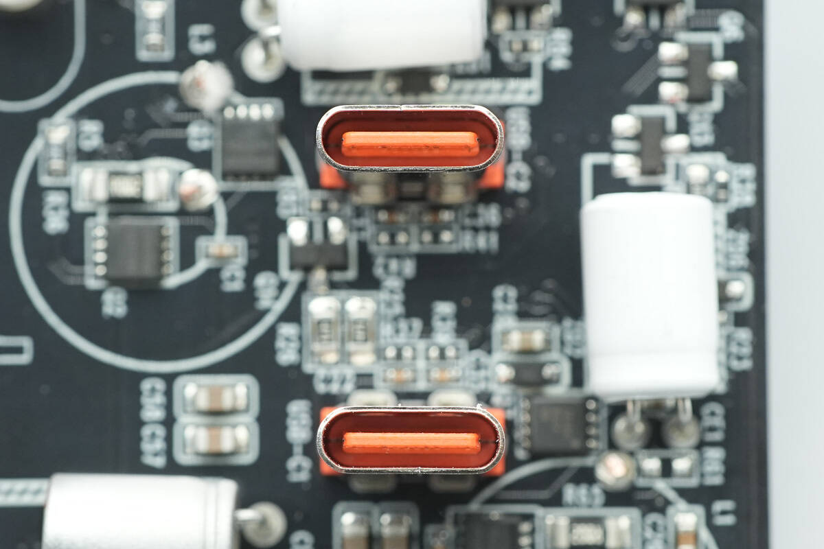
A close-up of the USB-C socket.
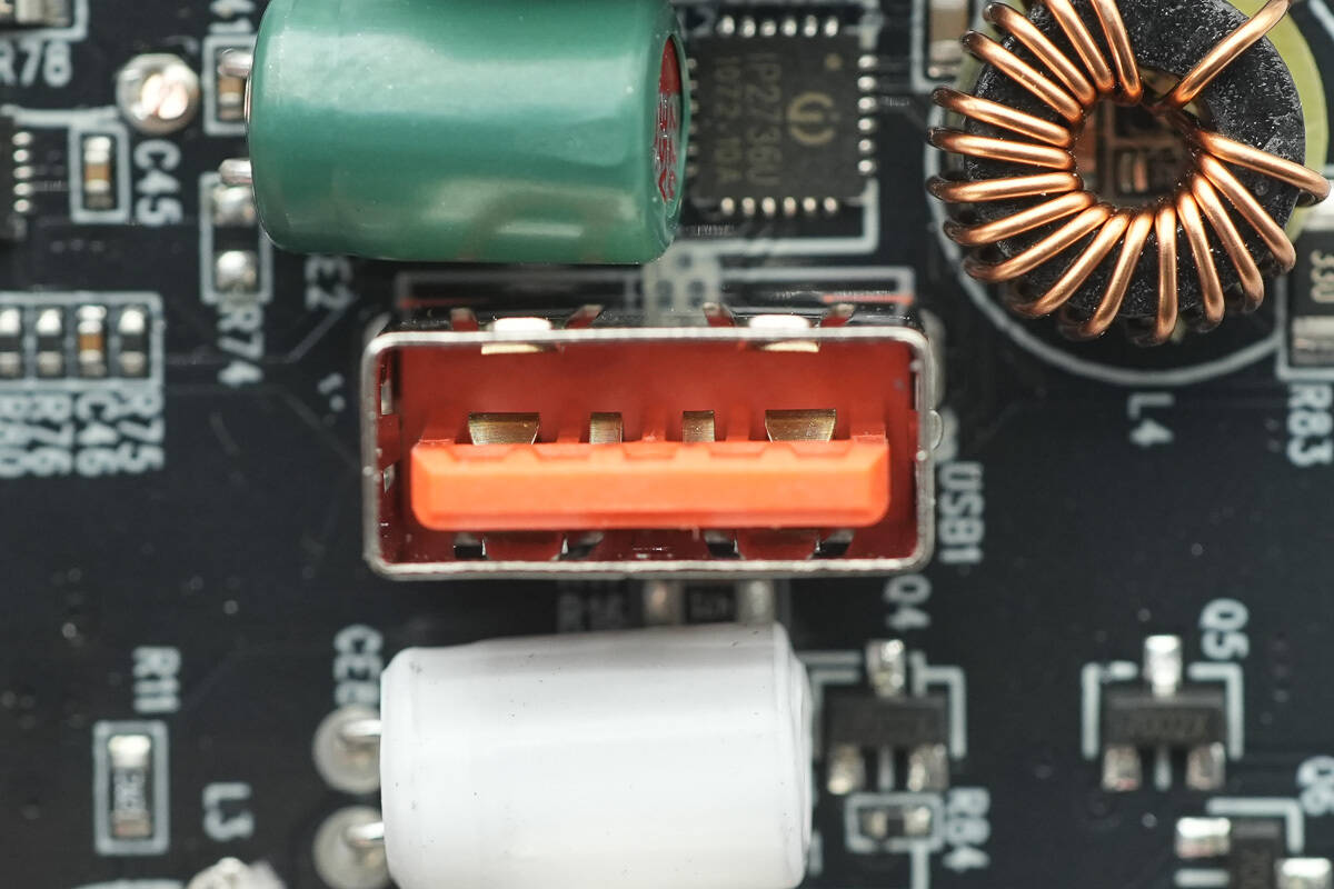
A close-up of the USB-A1 socket.
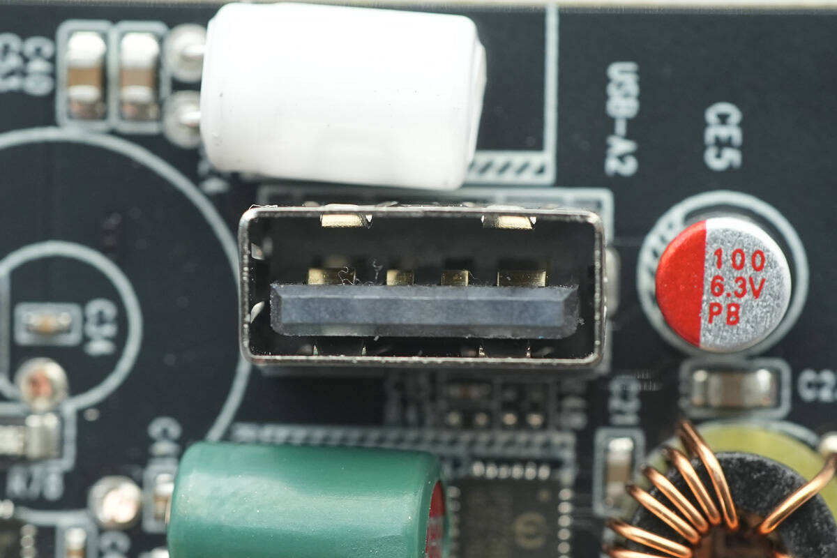
A close-up of the USB-A2 socket.
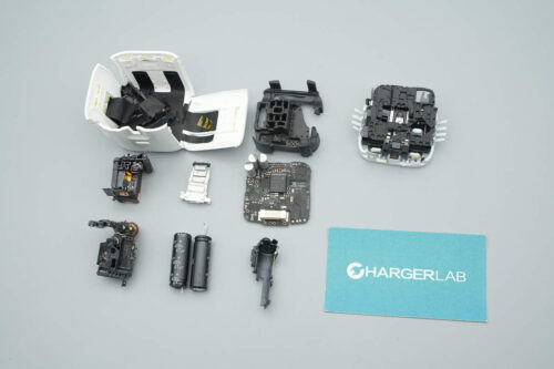
Well, those are all components of the Xiaomi 140W 8-in-1 Desktop Charging Station.
Summary of ChargerLAB
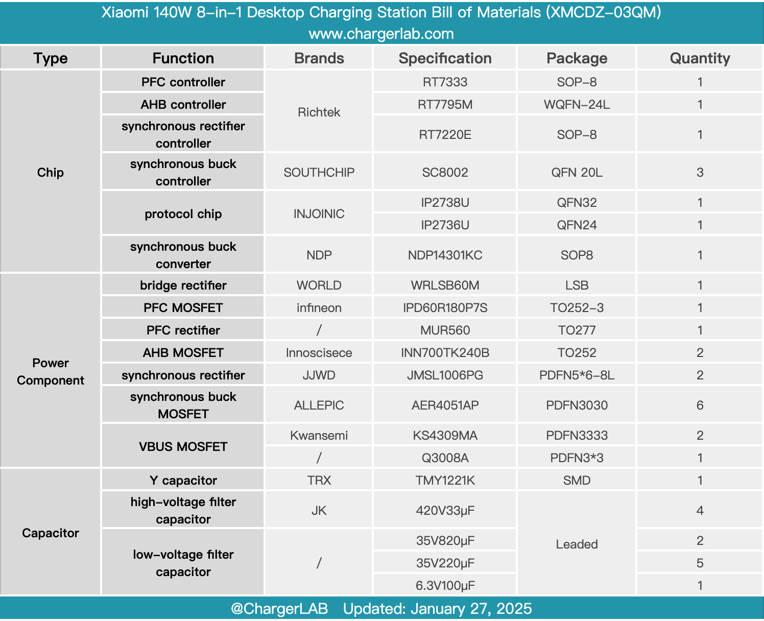
Here is the component list of the Xiaomi 140W 8-in-1 Desktop Charging Station for your convenience.
It addresses the core user demands for integrated desktop power supply, high performance, and aesthetic design. Combining an AC socket with a maximum load capacity of 2500W and a multi-port GaN fast charging module with a total power of 140W, it features 2 USB-C and 2 USB-A ports. It supports fast charging protocols such as Xiaomi's 120W Surge Fast Charging and PD3.1 140W. The independent low-current mode reflects consideration for users' diverse charging needs for various devices.
After taking it apart, we found that the internal structure is well-organized. The AC module uses a reliable single-piece copper strip, while the fast charging module employs a highly integrated active PFC (RICHTEK RT7333) combined with an AHB efficient architecture (RICHTEK RT7795M + Innoscience GaN FET), with synchronous rectification managed by the RICHTEK RT7220E.
The secondary buck conversion section utilizes the SouthChip SC8002 controller paired with ALLEPIC MOSFETs to achieve multiple independent, high-efficiency buck outputs. Protocol recognition is handled by the Injoinic IP2738U/IP2736U. The entire PCBA module is covered by a large metal heat dissipation plate and thermal pads, ensuring stable operation under high power density.
Overall, it is a well-designed, robustly built, and integrated product. It is not just a socket or charger; it is an intelligent power supply terminal that significantly enhances the desktop experience, combining safety, aesthetics, and powerful performance. For users who value a tidy desktop and have multiple device fast-charging needs, this is an extremely attractive and high-quality choice.
Related Articles:
1. Teardown of HONOR SuperCharge 66W Power Adapter (HN-110600CP0)
2. Teardown of Lenovo Thinkplus FLUXO 125W 12800mAh Portable Power Bank (PBFO-12125A)
3. Teardown of DJI Osmo Mobile 8 (DS308)