Introduction
Today, we are going to tear down the charger that comes with the vivo X200 and S20 series. It utilizes GaN technology, featuring a maximum output power of 90W, and is compact compared to traditional chargers. Although the output port is USB-A, it supports charging protocols such as QC and UFCS. Next, let's take it apart to see its internal components and structure.
Product Appearance
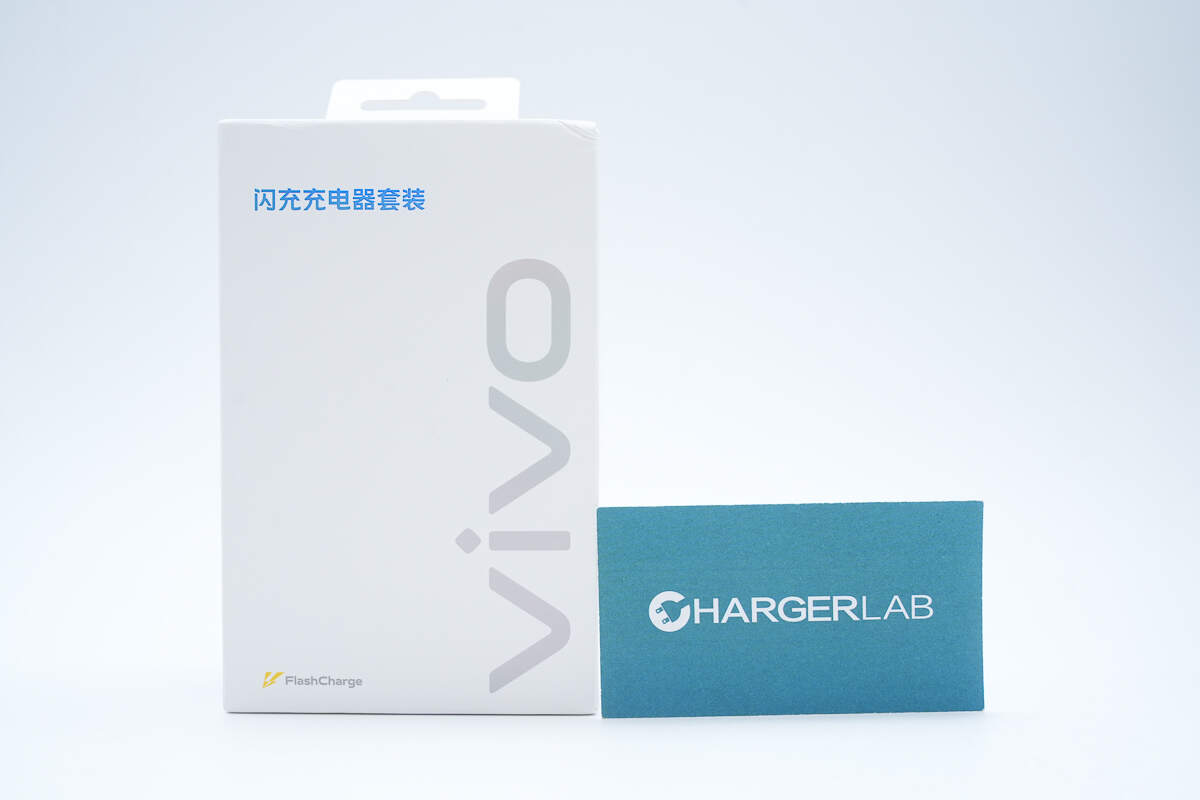
The vivo logo is printed on the front of the box.
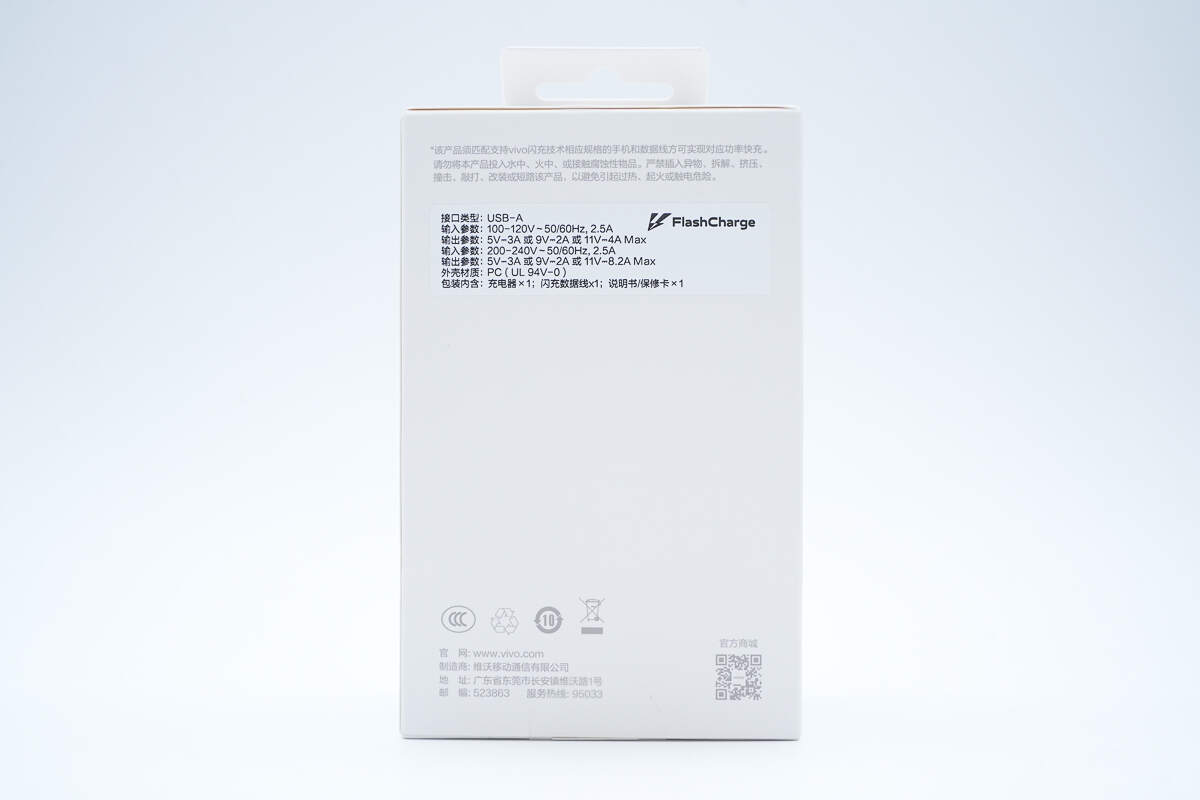
The specs info is printed on the back.
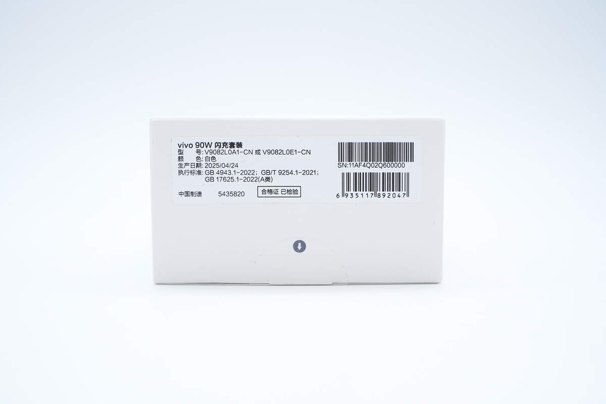
The sticker on the bottom displays information such as the model, color, and manufacturing date.
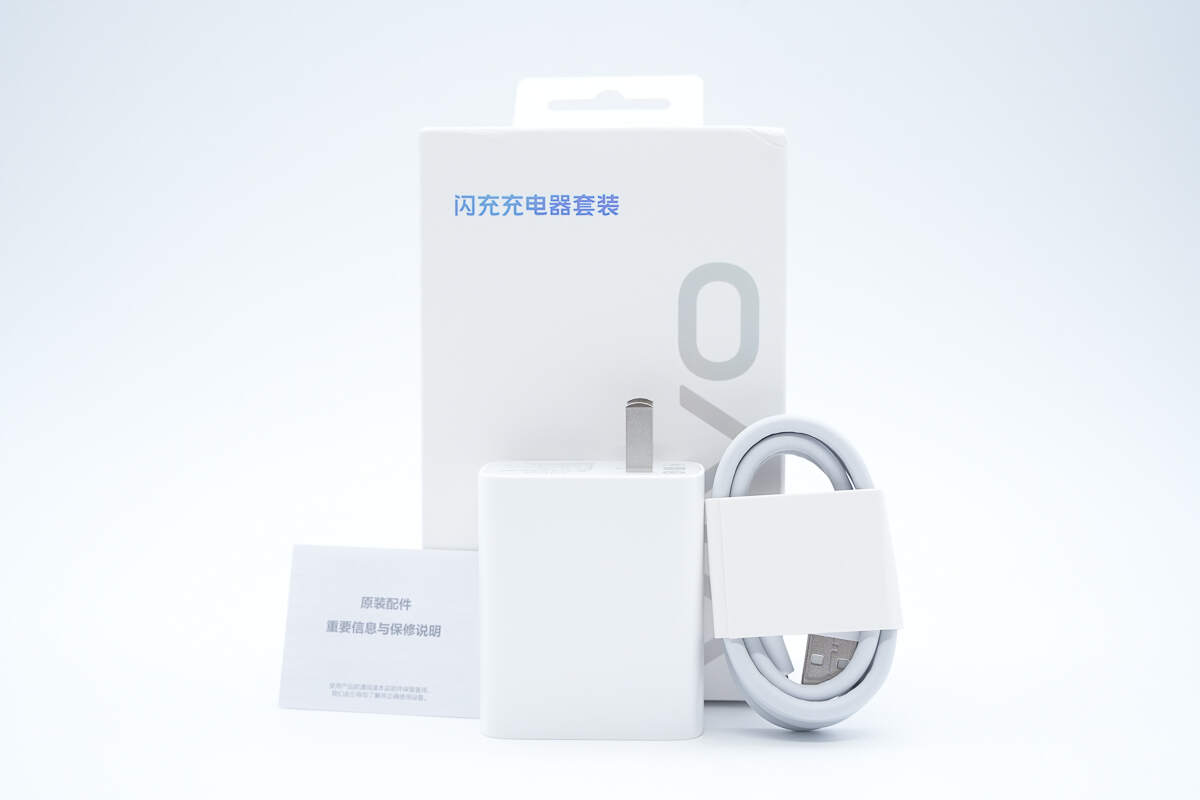
The box contains the charger, cable, and some documents.
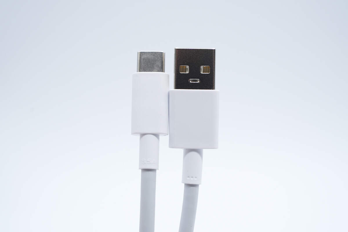
The USB-A to USB-C cable supports a current of up to 8.5A.
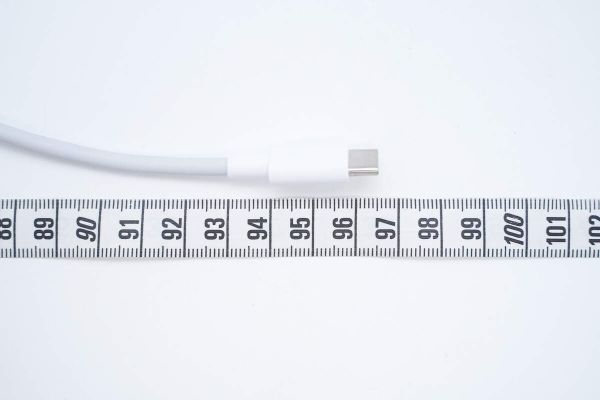
The length is about 96.5 cm (37.99 inches).
The casing is made of flame-retardant PC material.
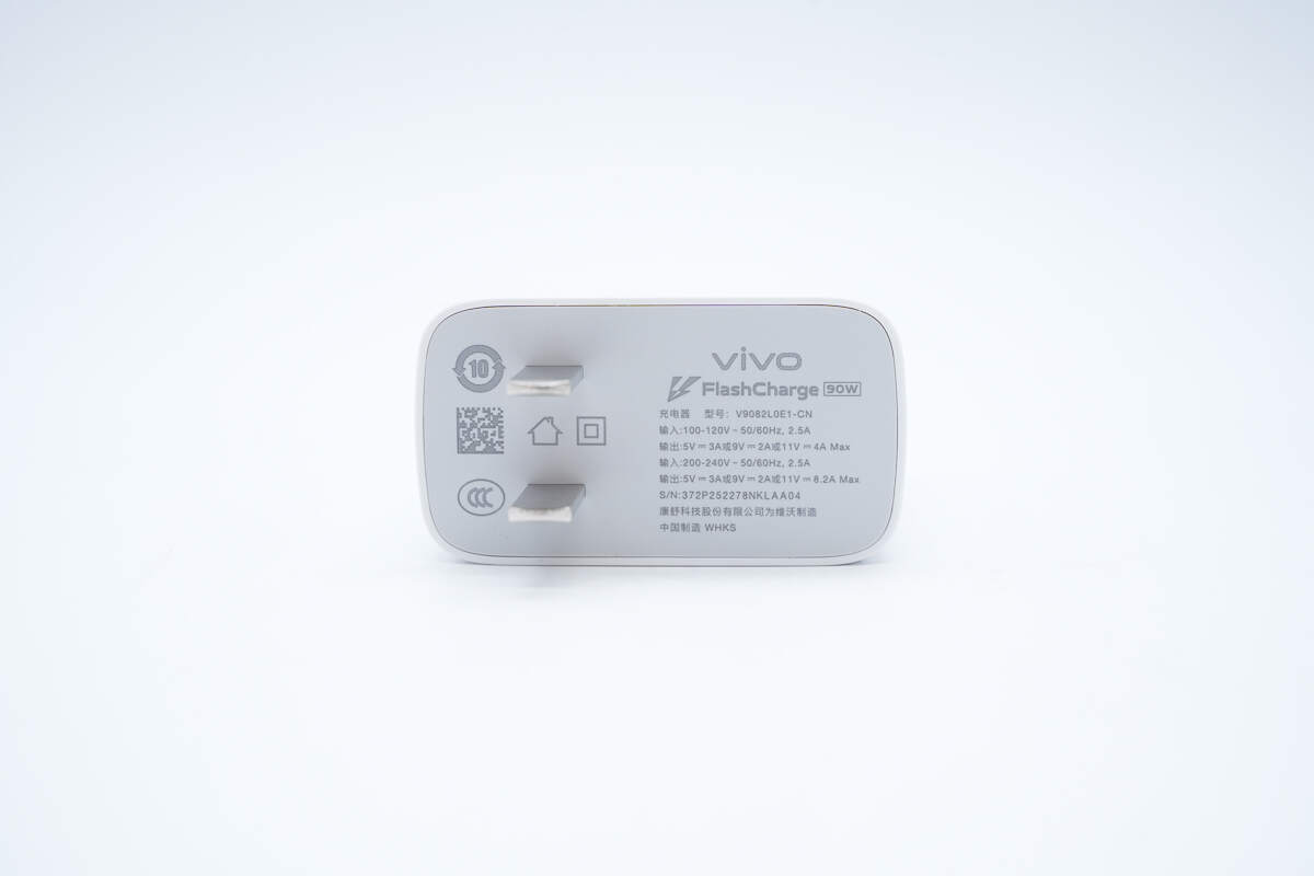
The input end is also printed with spec info.
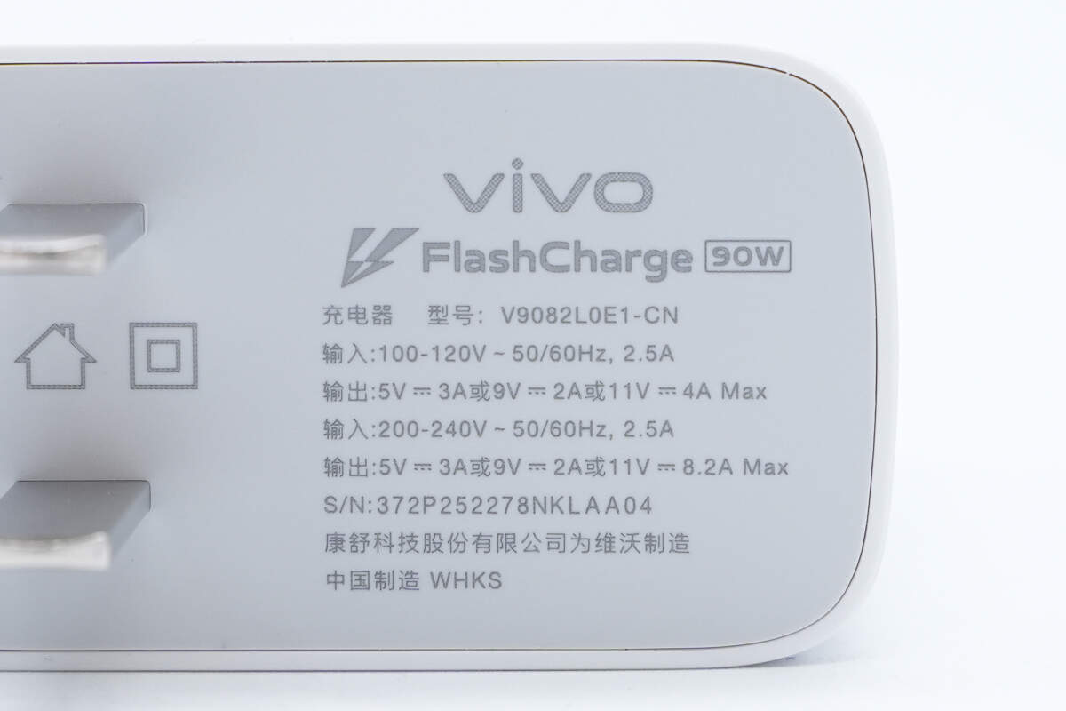
Model: V9082L0E1-CN
Input: 100-240V~50/60Hz 2.5A
Output: 5V3A, 9V2A, 11V4A Max
Input: 200-240V~50/60Hz 2.5A
Output: 5V3A, 9V2A, 11V8.2A Max
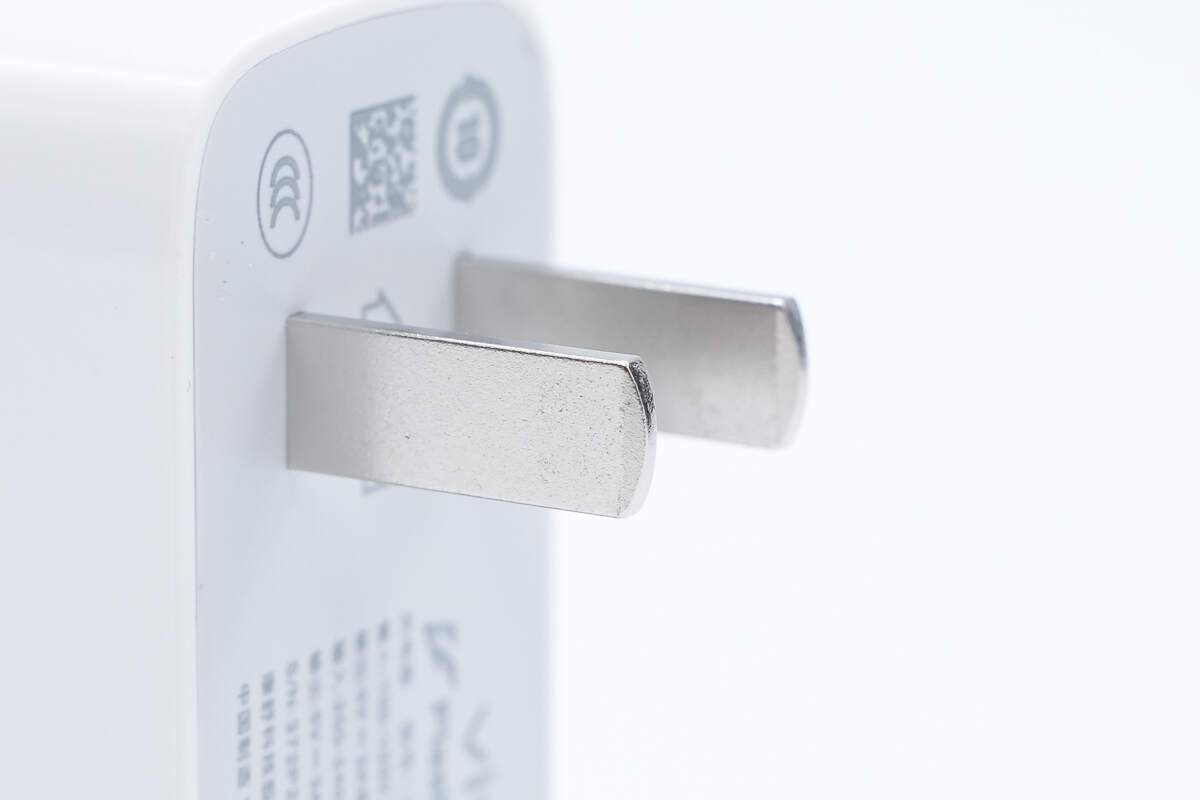
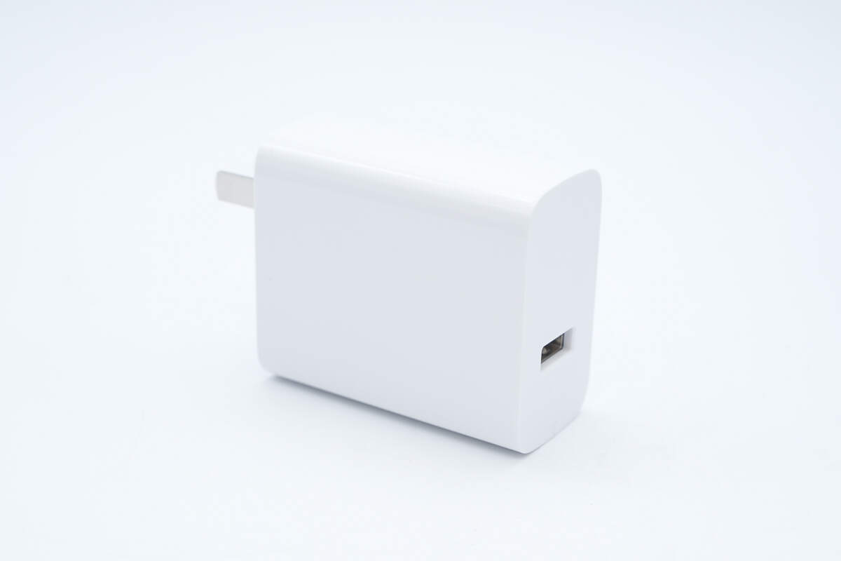
It is equipped with fixed prongs.
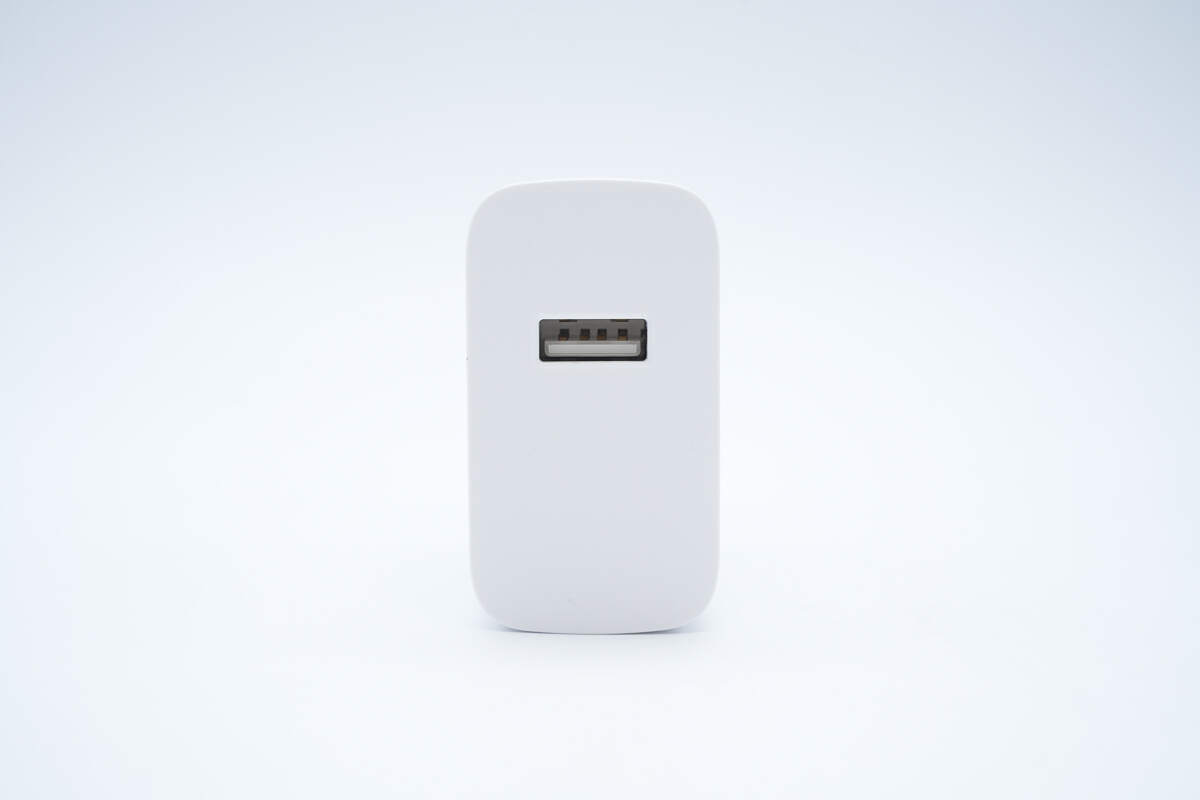
The output port is a single USB-A.
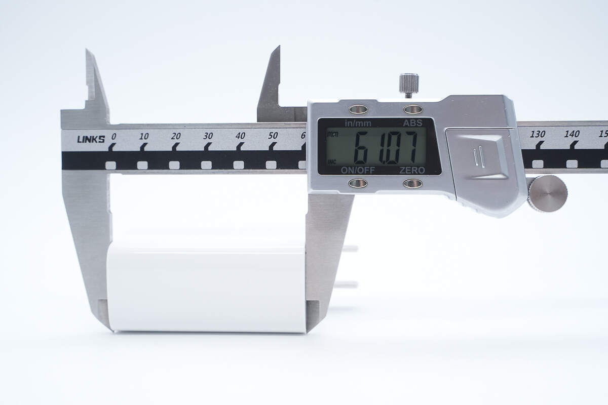
The length is about 61.07 mm (2.4 inches).
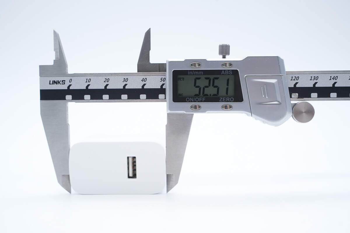
The width is about 52.51 mm (2.067 inches).
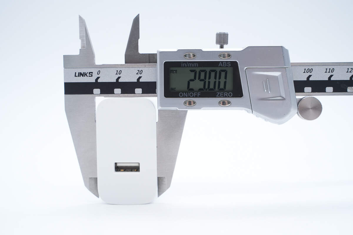
The thickness is about 29 mm (1.14 inches).
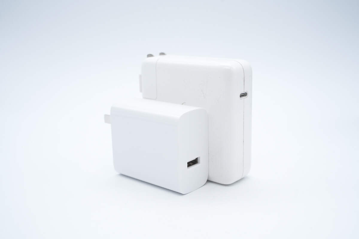
It is significantly smaller than the Apple 96W charger.
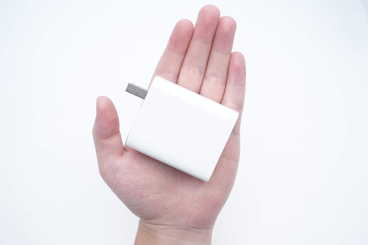
That's how big it is in the hand.
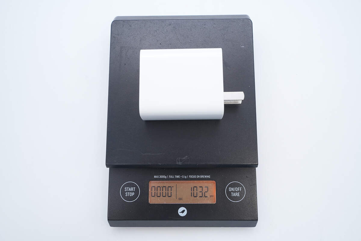
The weight is about 103 g (3.63 oz).
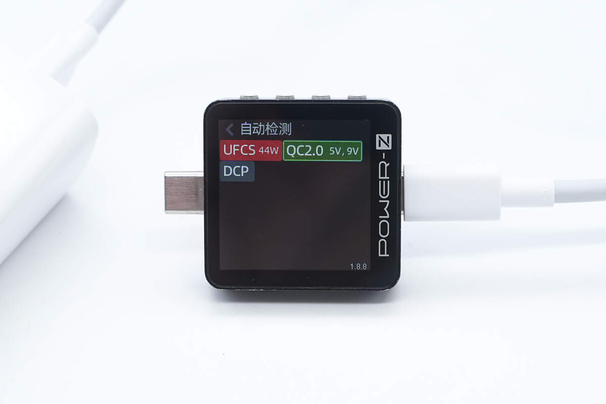
ChargerLAB POWER-Z KM003C shows it supports UFCS, QC2.0, and DCP protocols.
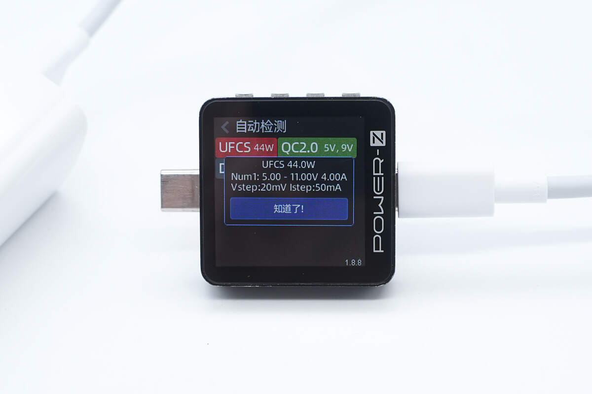
It supports a UFCS voltage range of 5–11V at 4A.
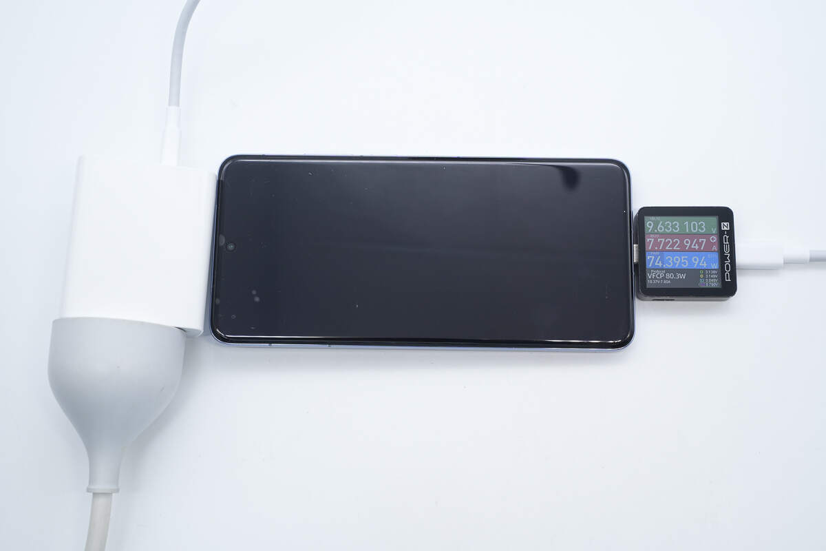
Using it to charge the vivo X200 Pro, the power is about 74.4W.
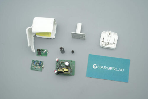
Teardown
Next, let's take it apart to see its internal components and structure.
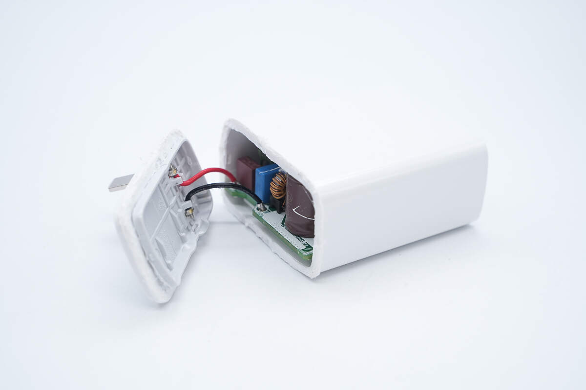
Cut open the casing at the input end.
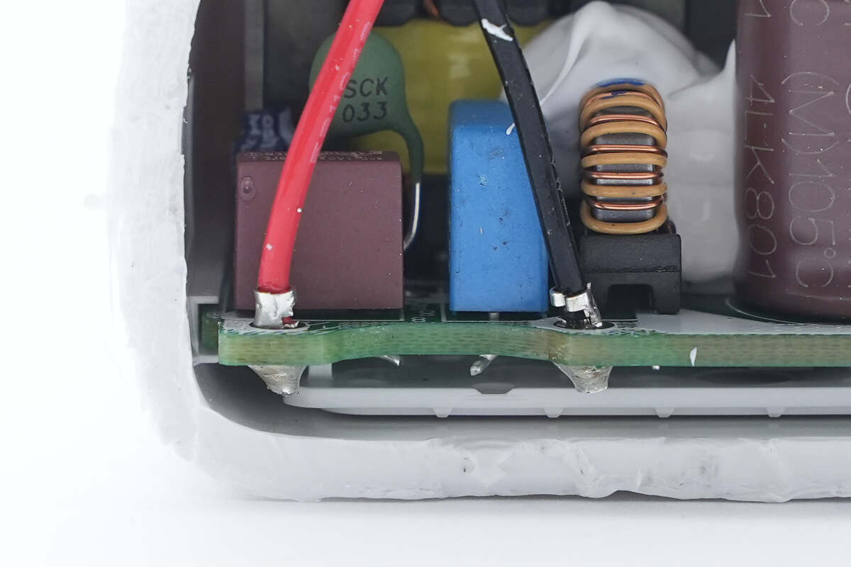
The connection wires are cold-pressed and soldered to terminals.
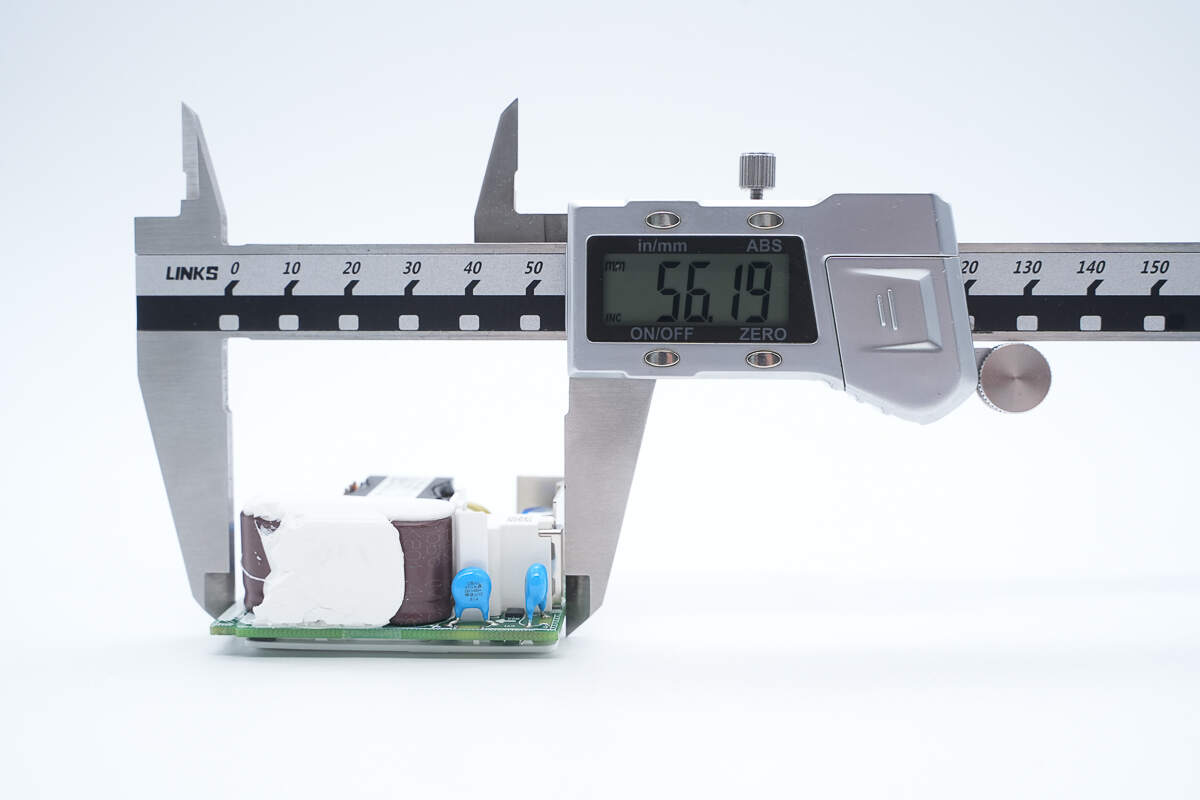
The length of the PCBA module is about 56.19 mm (2.21 inches).
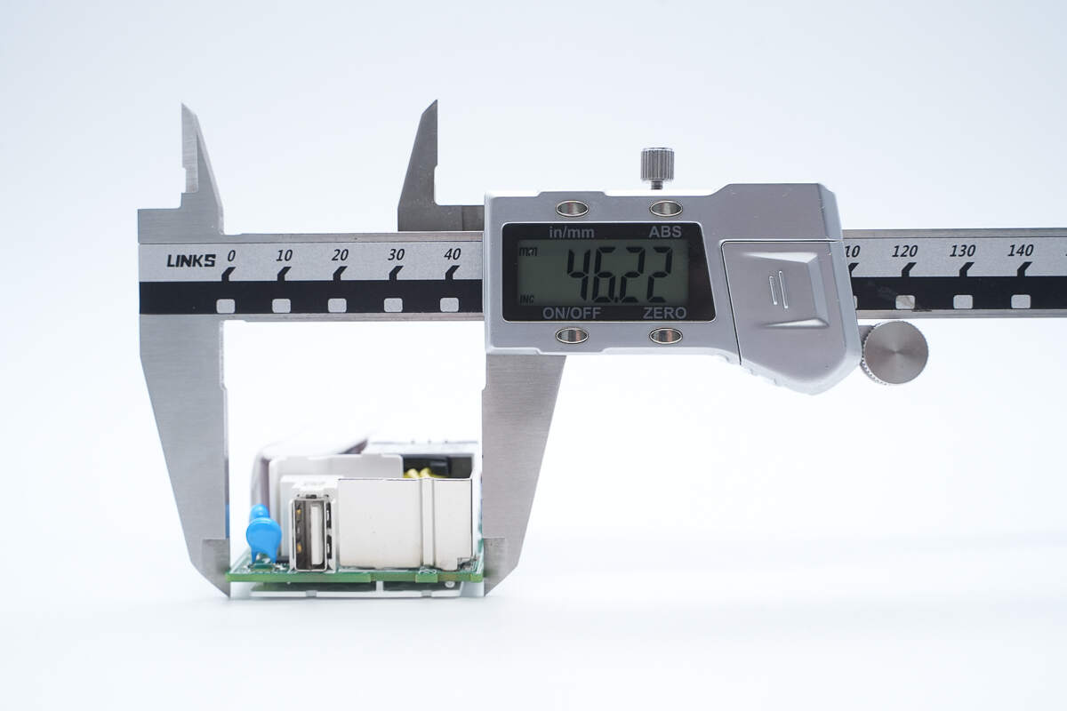
The width is about 46.22 mm (1.82 inches).
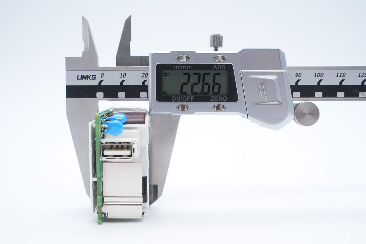
The thickness is about 22.66 mm (0.89 inches).
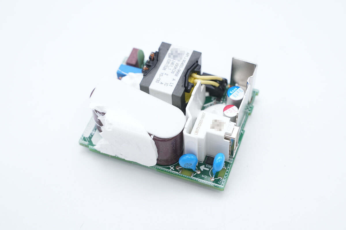
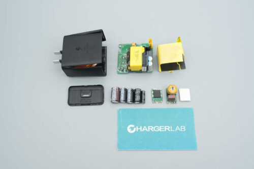
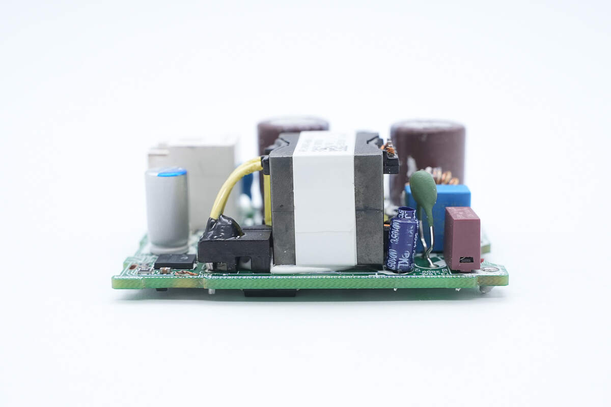
A sponge is attached to the top of the capacitors. A plastic isolation plate is placed between the primary and secondary sides. The USB-C socket is reinforced with a plastic housing, and a metal heatsink is also installed to dissipate heat from the synchronous rectifier.
The gaps are filled with potting compound.
The back is covered with a plastic plate and a metal heatsink.
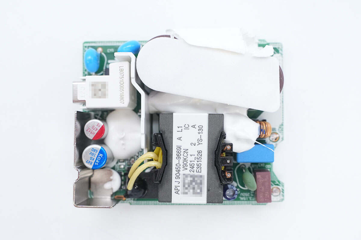
Remove the metal heatsink, part of the back is also filled with potting compound for reinforcement.
Remove the insulation board, metal plate, and potting compound.
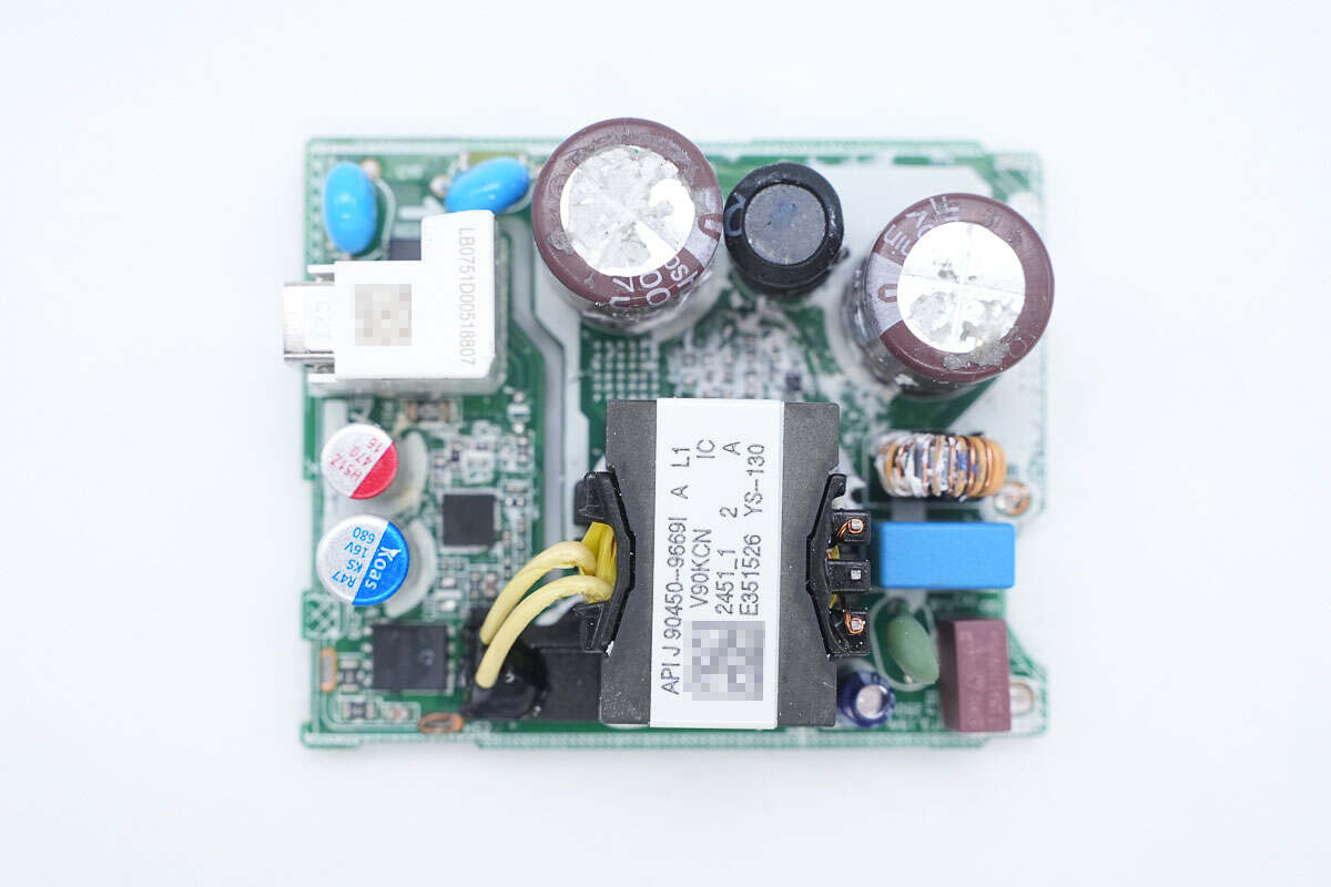
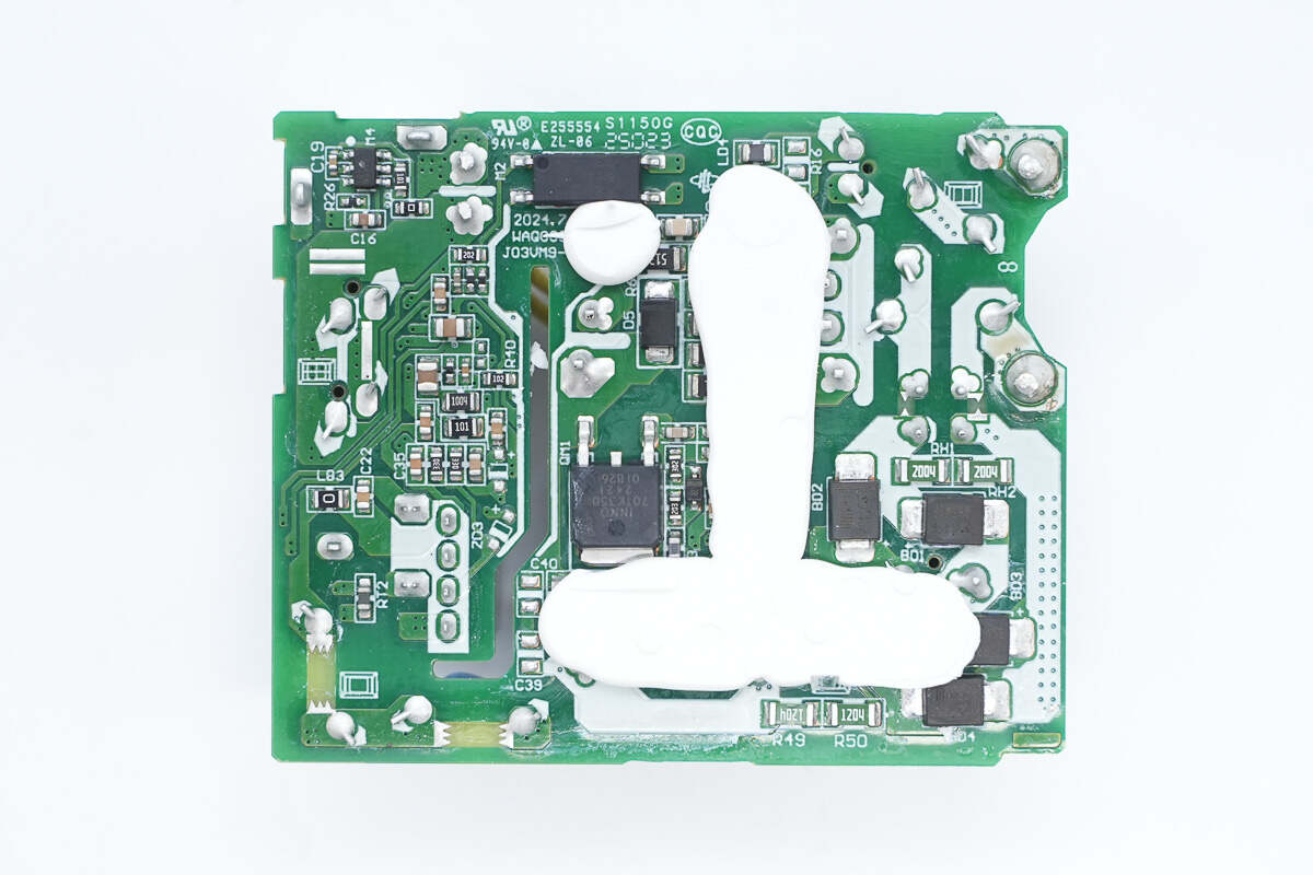
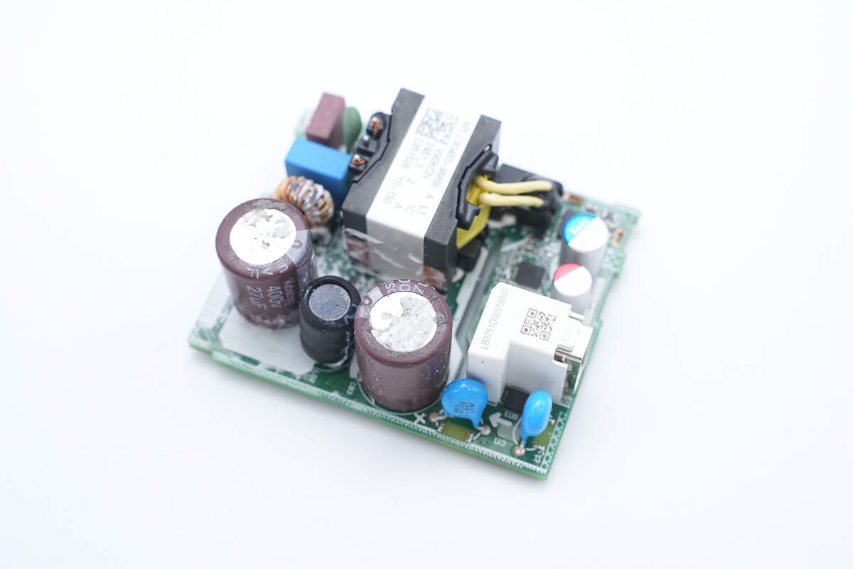
On the front of the PCBA module, there are components such as a fuse, common mode choke, electrolytic capacitors, and a transformer.
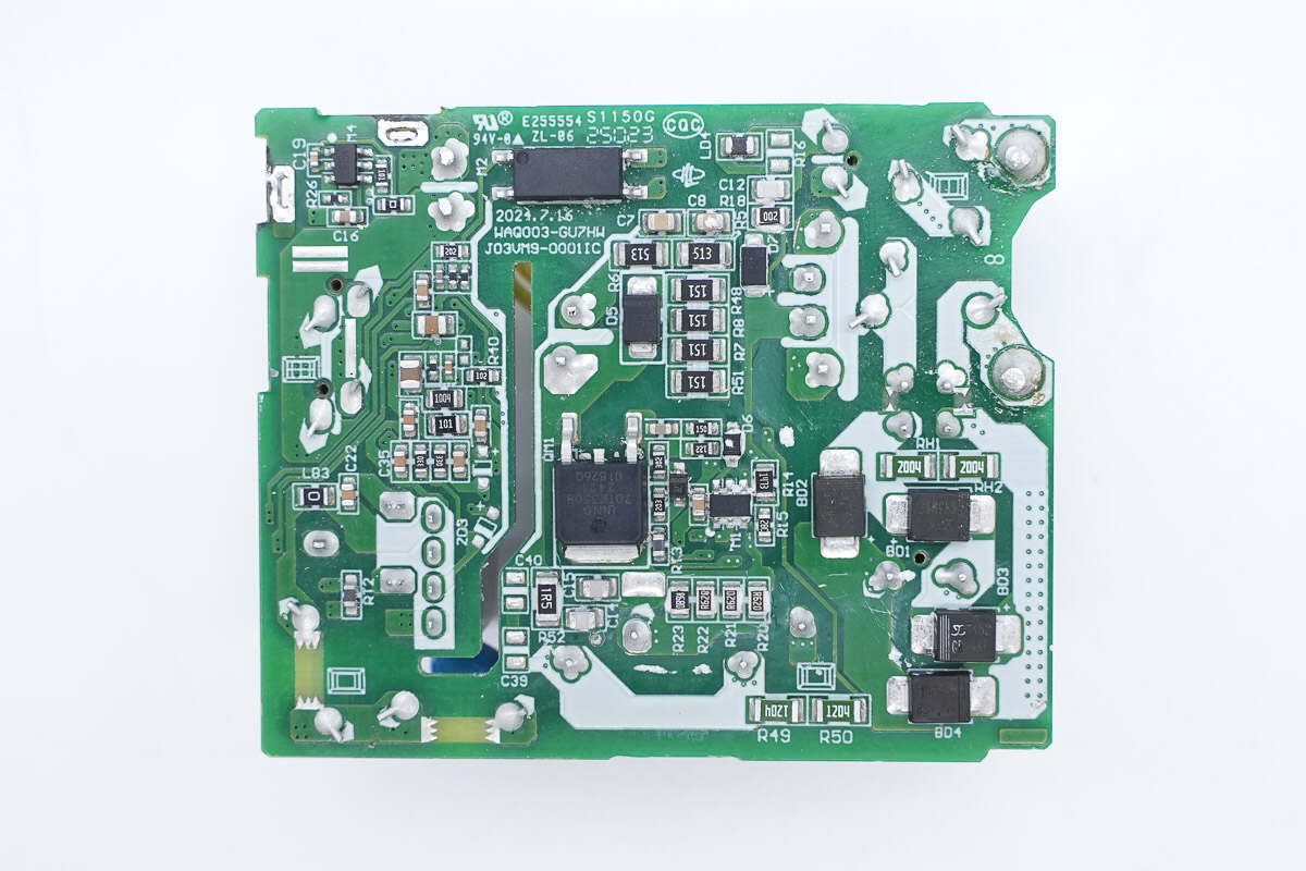
There are primary MOSFET, optocoupler, and synchronous rectifier controller on the back.
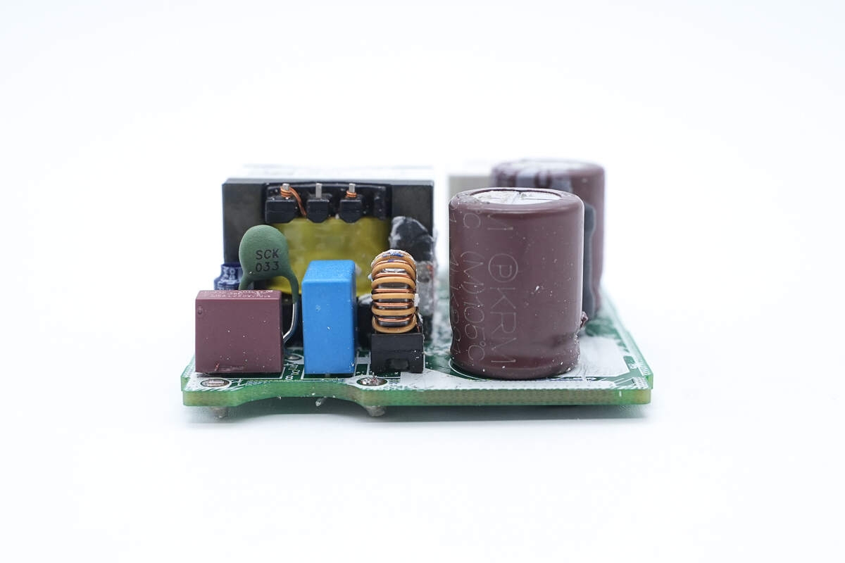
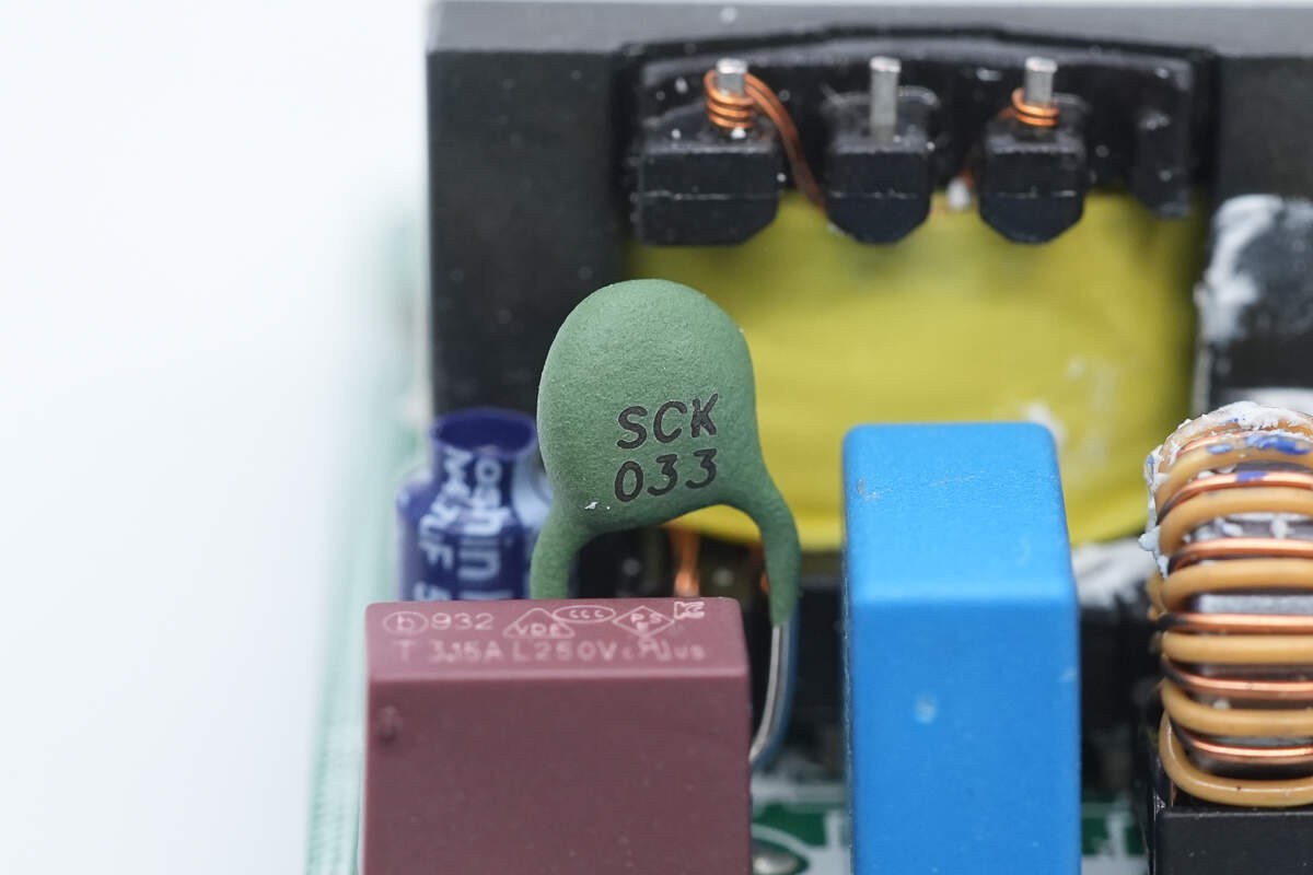
The input side features a time-delay fuse, NTC thermistor, safety X2 capacitor, and a common mode choke.
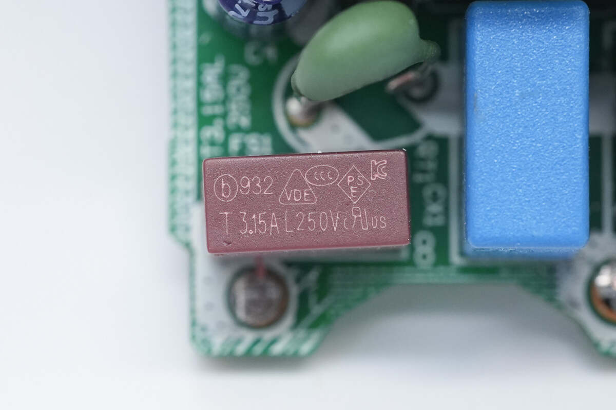
The time-delay fuse is from Betterfuse. 3.15A 250V.
The NTC thermistor is used to suppress inrush current when powered on.
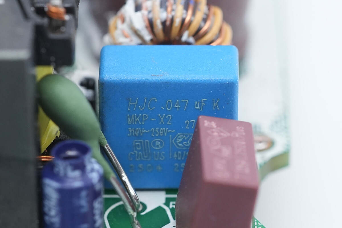
The safety X2 capacitor is from HJC. 0.47μF.
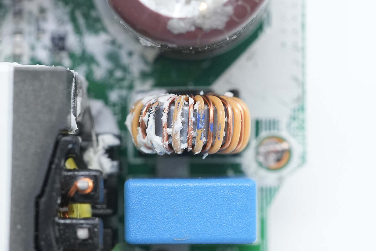
The common mode choke is wound with dual wires and is used to filter out EMI interference.
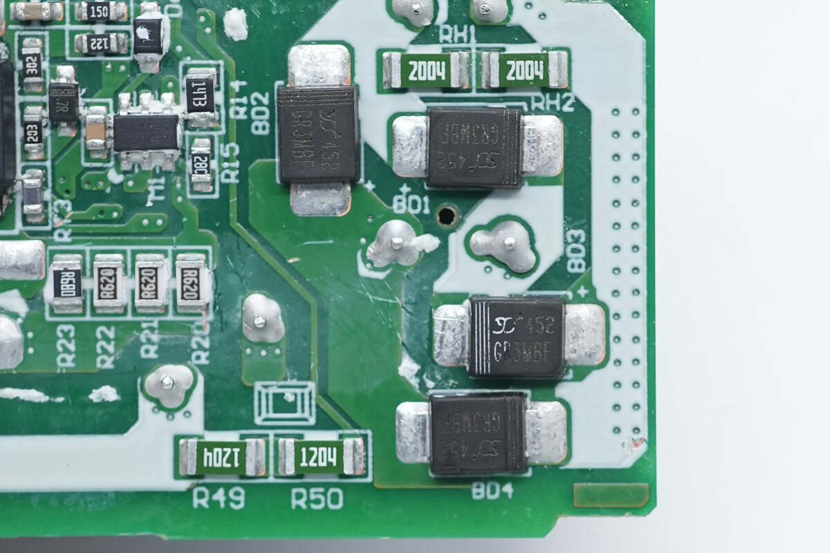
It uses four GR3MBF rectifiers configured as a bridge rectifier.
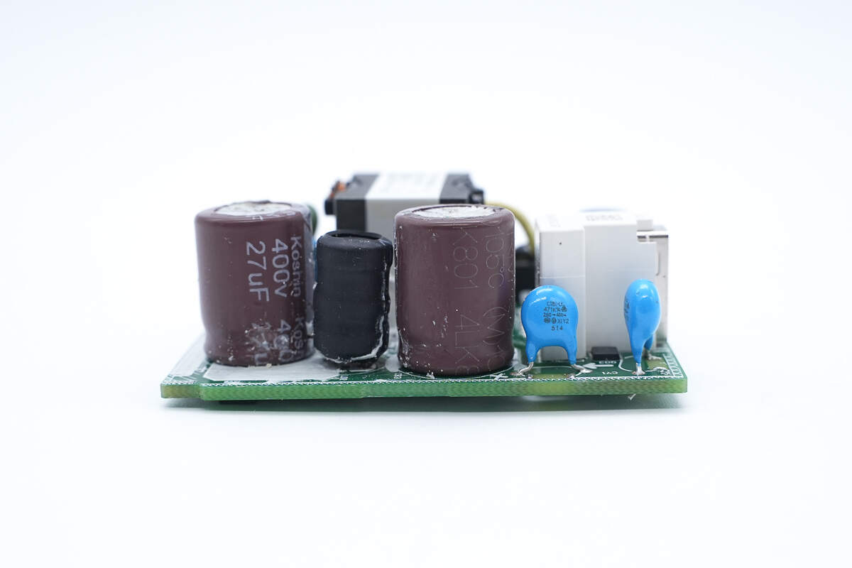
This side has two electrolytic capacitors and an I-shaped inductor.
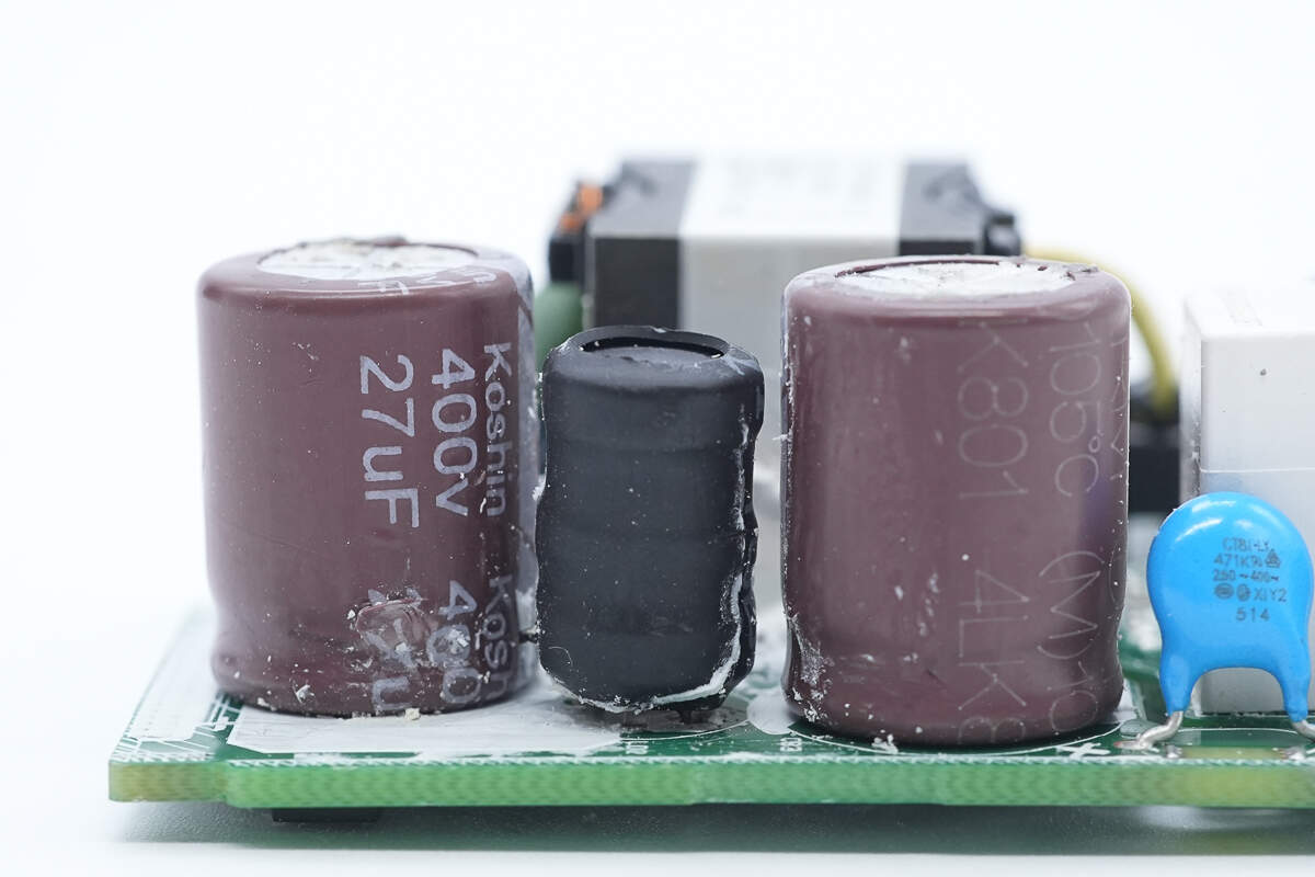
These two electrolytic capacitors are from Koshin. 400V 27μF.
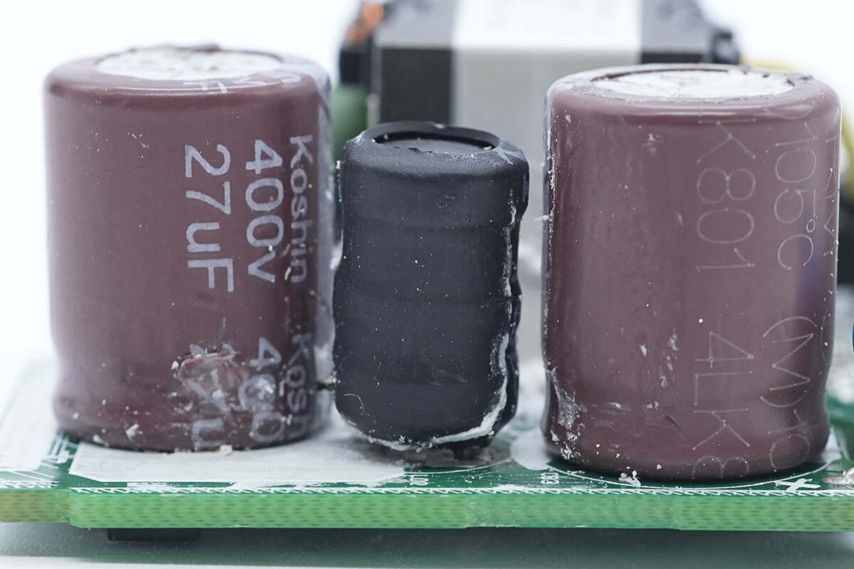
The I-shaped inductor is insulated by heat-shrinkable tubing.
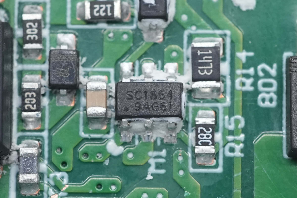
The primary master control chip is from SouthChip. Model is SC1854.
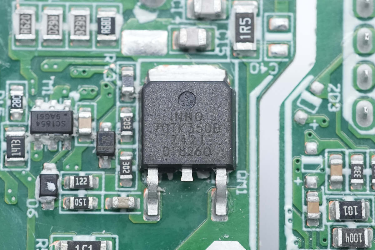
The primary MOSFET is from Innoscience. It is a 700V-rated enhancement-mode GaN FET, with a device voltage rating of 700V and a transient voltage rating of 800V. It has an on-resistance of 350mΩ. It supports ultra-high switching frequencies, has no reverse recovery charge, and features extremely low gate charge and output charge. It meets JEDEC standards for industrial applications, includes built-in ESD protection, and complies with RoHS, lead-free, and EU REACH regulations. Model is INN700TK350B.
It adopts the TO252 package. It features enhanced thermal conductivity and can be used in power supply PFC applications, asymmetric half-bridge/LLC/flyback switching power supplies, DC-DC conversion, LED lighting, fast battery charging, laptop adapters, computer power supplies, and high-efficiency, high-power-density power conversion applications such as electric tools.
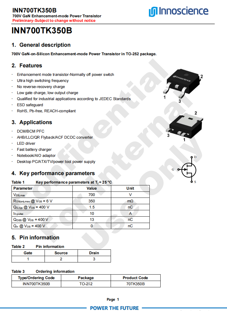
Here is the information about Innoscience INN700TK350B.
On the other side of the PCBA module, there is the capacitor that supplies power to the master control chip, as well as the transformer.
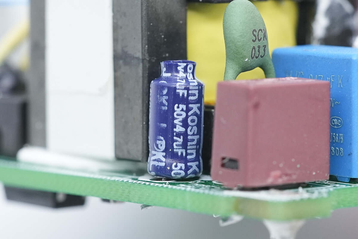
The capacitor that powers the master control chip is from Koshin. 50V 4.7μF.
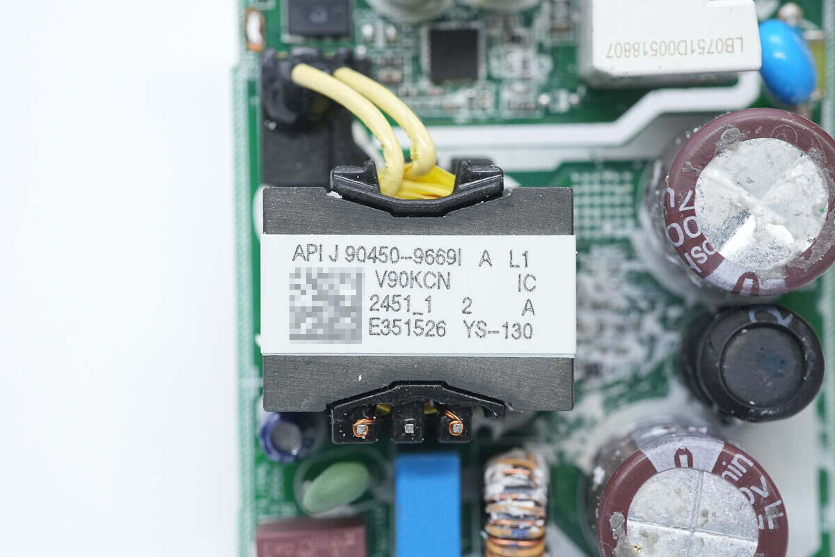
There is the transformer.
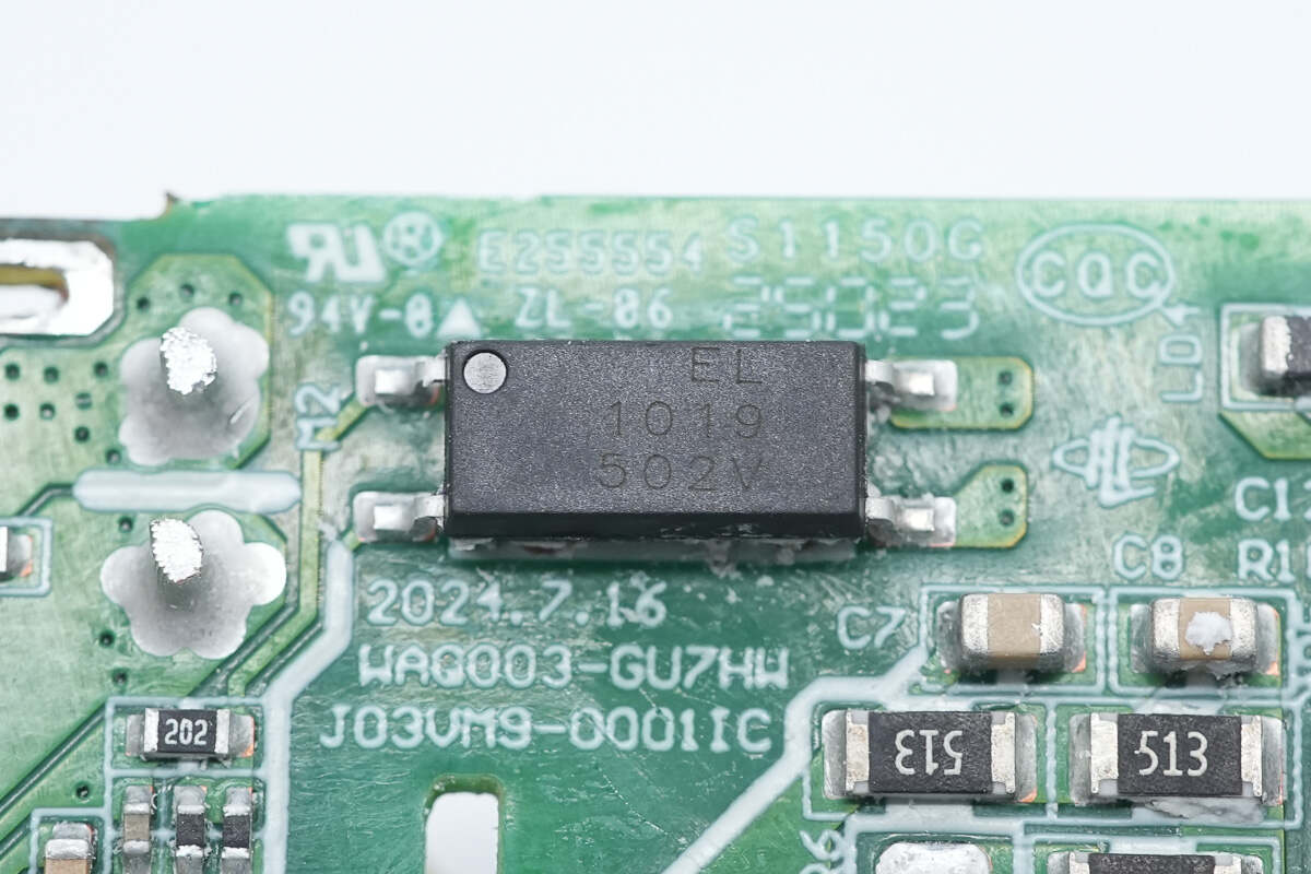
The Everlight EL 1019 optocoupler is used for output voltage feedback.
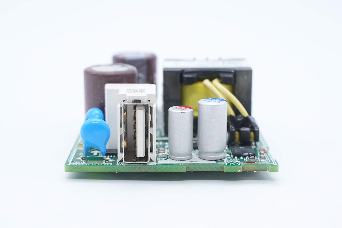
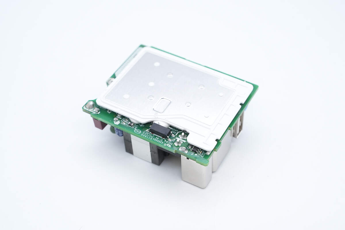
The output side includes blue Y capacitors, solid capacitors, a synchronous rectifier, a protocol chip, and an output VBUS MOSFET, among others.
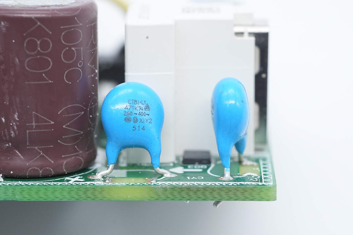
There are two blue Y capacitors.
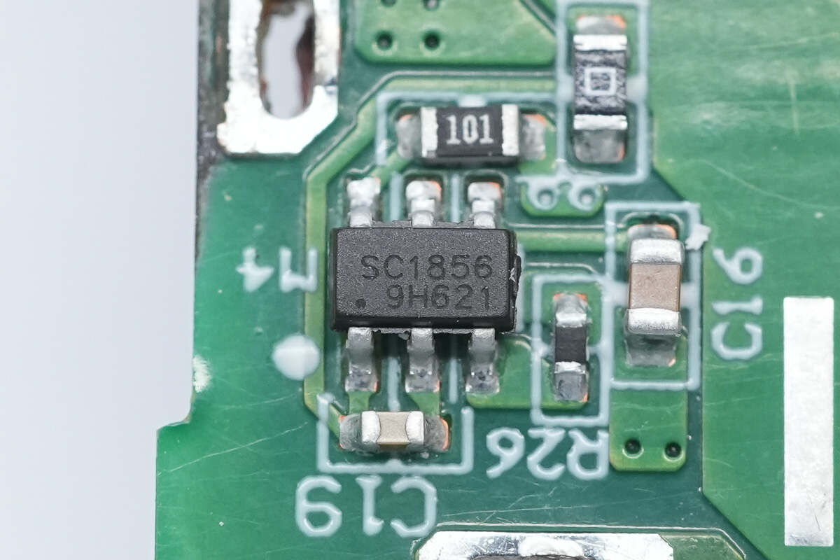
The synchronous rectifier controller is from SouthChip. Model is SC1856.
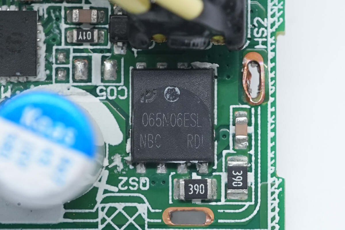
The synchronous rectifier is from Pingwei and adopts the DFN5*6 package. 60V 5mΩ. Model is PW065N06ESL.
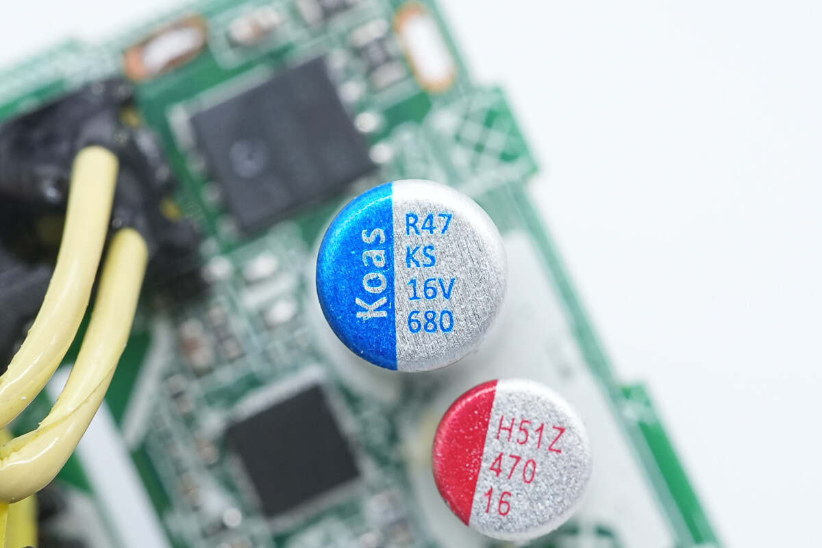
This solid capacitor is from Koshin. 16V 680μF.
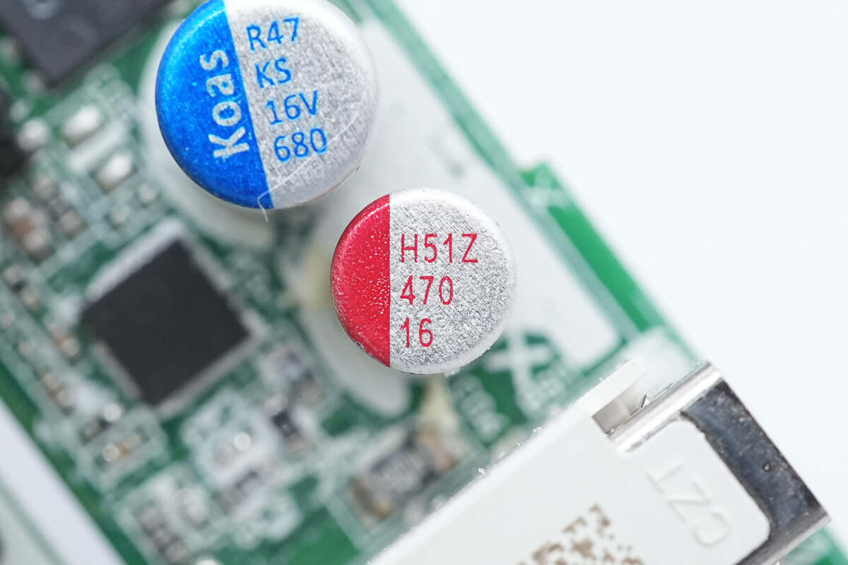
This is the other solid capacitor. 16V 470μF.
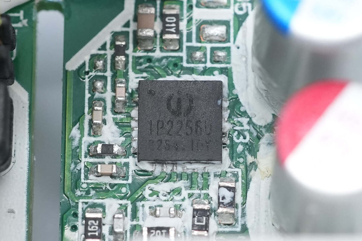
The protocol chip is from Injoinic. It is an integrated fast-charging protocol control IC designed for USB ports, supporting multiple fast-charging protocols including USB Type-C DFP, PD 2.0/PD 3.1/PPS, HVDCP QC5/QC4+/QC3+/QC3.0/QC2.0, UFCS, Apple 2.4A, BC1.2, and SAMSUNG 2.0A. This chip provides a complete solution for unidirectional output applications such as adapters and car chargers. With high integration and rich functionality, it requires minimal external components, effectively reducing overall solution size and lowering BOM costs. Model is IP2256U.
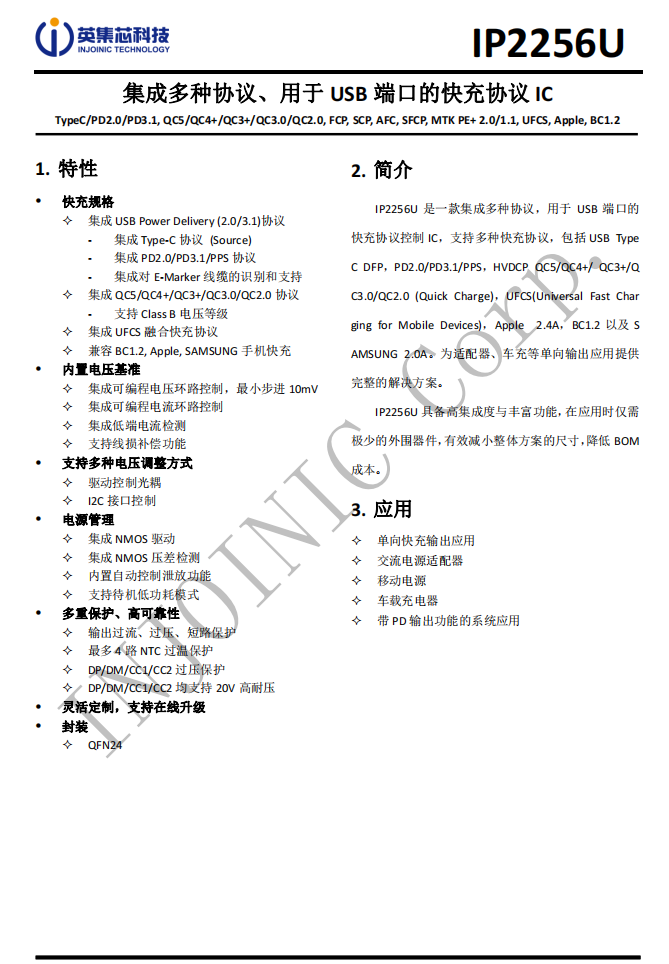
There is information about Injoinic IP2256U.
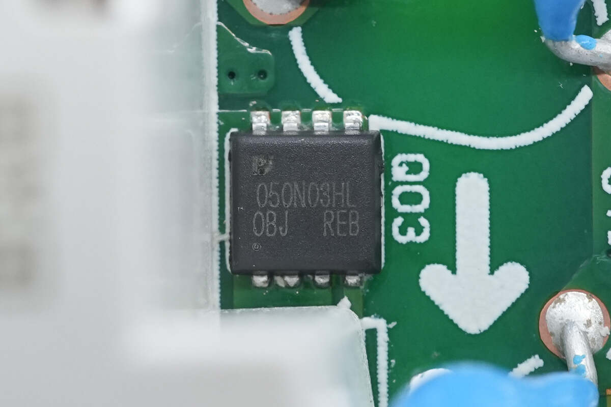
The output VBUS MOSFET is from Pingwei, marked with 050N03HL.
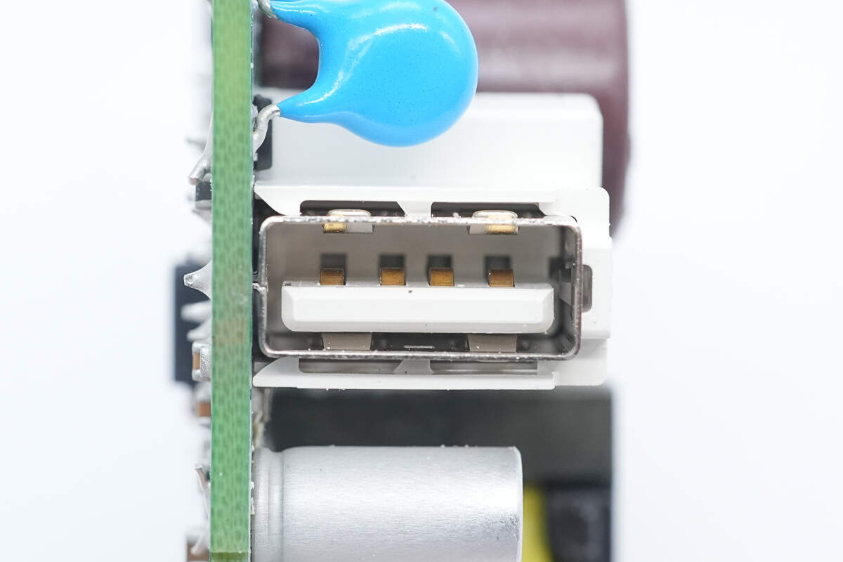
There is the USB-A socket.
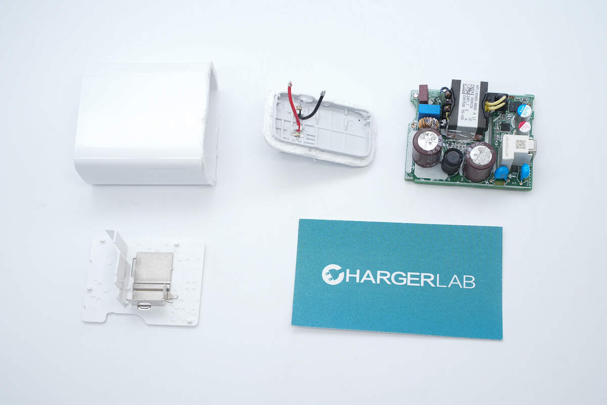
Well, those are all components of the vivo 90W FlashCharge GaN Charger.
Summary of ChargerLAB
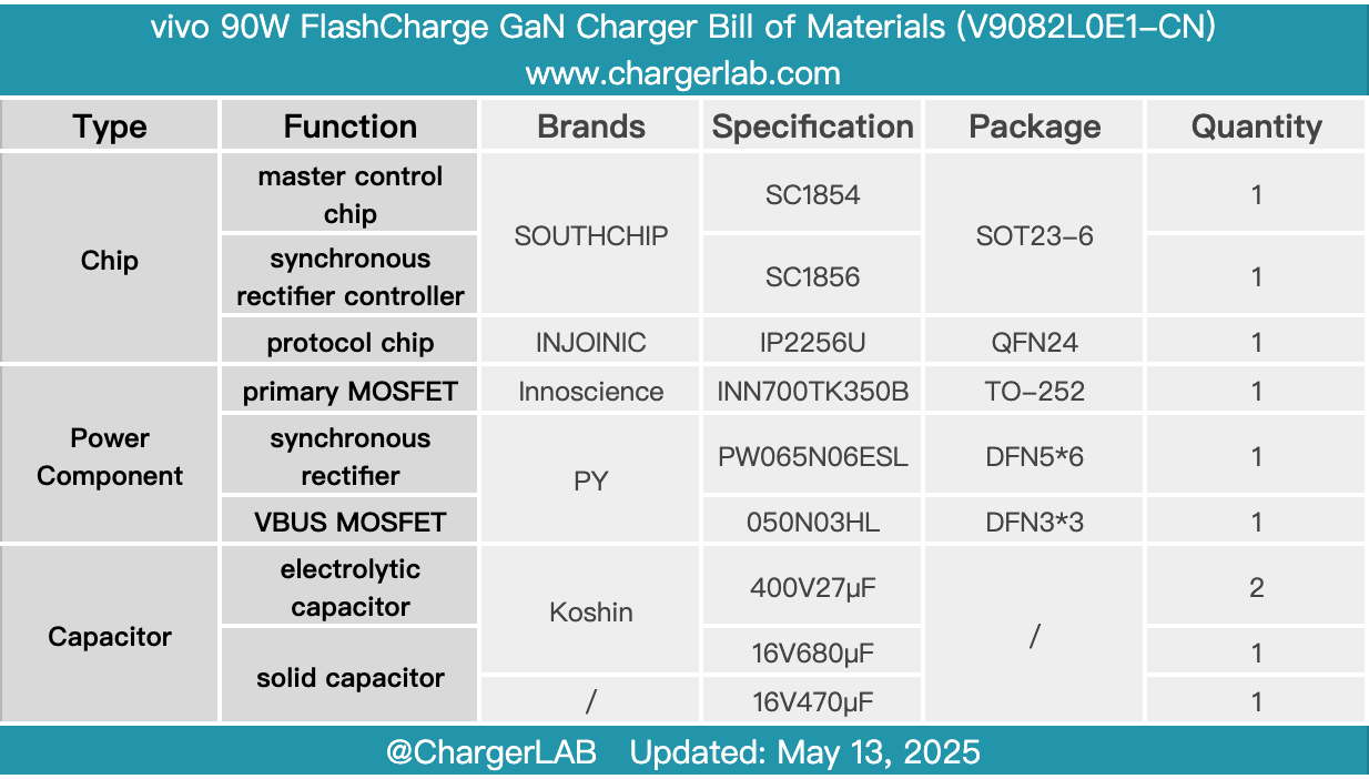
Here is the component list of the vivo 90W FlashCharge GaN Charger for your convenience.
It features a classic design and comes with a cable that supports a high current of 8.5A. It offers protection, including over-voltage and over-current.
After taking it apart, we found that it uses the SouthChip SC1854+SC1856 high-frequency QR flyback power architecture, paired with the Innoscience INN700TK350B GaN FET and Pingwei synchronous rectifier. Additionally, it employs the Injoinic 2256U protocol chip to control the output. In terms of build quality, components like capacitors and connectors are reinforced, and the synchronous rectifier is equipped with a dedicated heatsink for cooling.
Related Articles:
1. Teardown of Xiaomi 90W GaN Pudding Charger (MDY-18-EU)
2. Teardown of Huawei Pura X Original 66W GaN Charger (HW-110600C05)
3. Teardown of ANKER 253W GaN Power Adapter