Introduction
vivo has released a 120W GaN charger equipped with two USB-C ports and one USB-A port. It supports 11V/8.2A, 20V/6A, and 100W PD. The charger can charge the vivo X300 to 56% and the iPhone 16 to 59% within 30 minutes.
It is compatible with UFCS, PPS, PD 3.0, and other fast charging protocols, supporting multiple output configurations such as 90W+10W+10W and 55W+55W+10W. Below, we take a closer look at the internal components and design.
Product Appearance
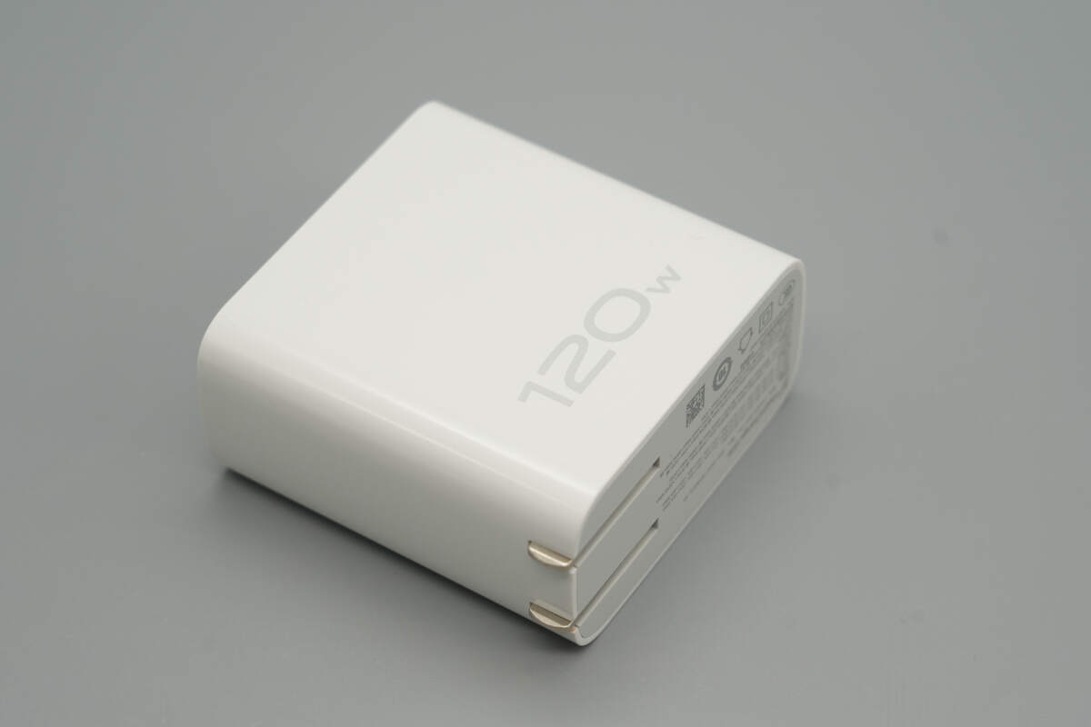
The casing is made of flame-retardant PC material with a glossy finish, featuring smooth rounded transitions on both sides.
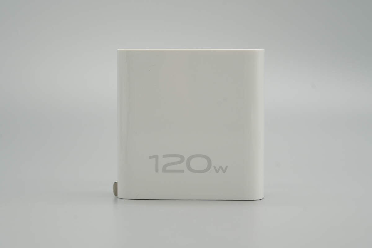
The front is marked with "120W."
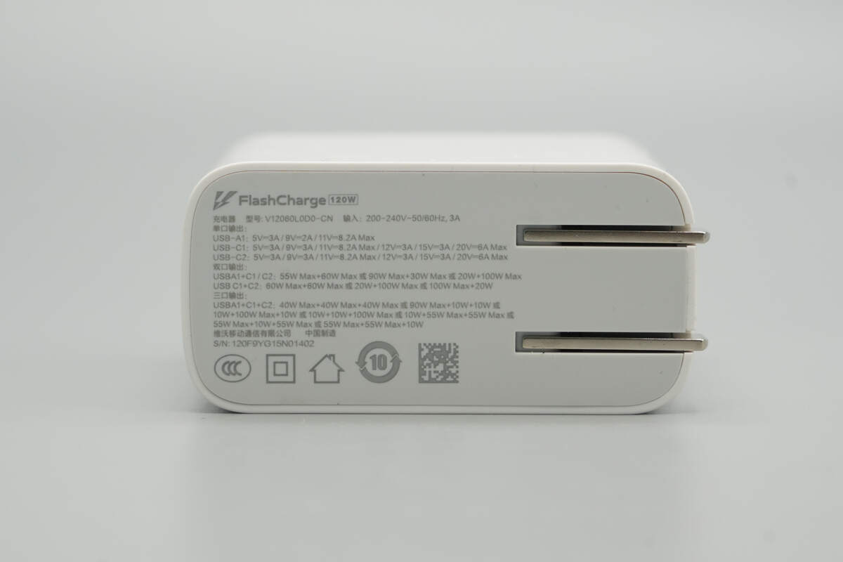
The input side is printed with the specification details.
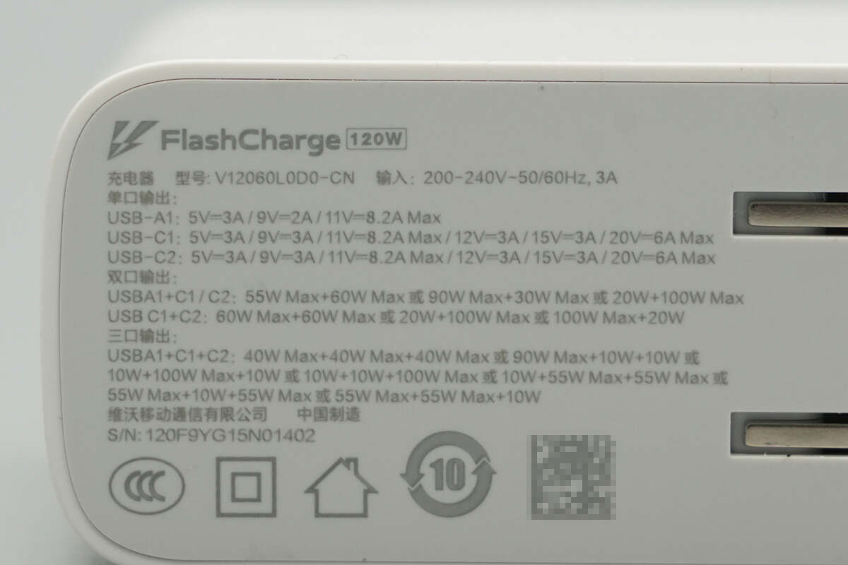
Model: V12060L0D0-CN
Input: 200-240V~ 50/60Hz 3A
Single port output:
USB-A1: 5V/3A, 9V/3A, 11V/8.2A Max
USB-C1/C2: 5V/3A, 9V/3A, 11V/8.2A, 12V/3A, 15V/3A, 20V/6A Max
Dual port output:
USB-A1 + C1/C2: 55W + 60W or 90W + 30W or 20W + 100W Max
USB-C1 + C2: 60W + 60W or 20W + 100W or 100W + 20W
Triple port output:
USB-A1 + C1 + C2: 40W + 40W + 40W or 90W + 10W + 10W or 10W + 100W + 10W or 10W + 10W + 100W or 10W + 55W + 55W or 55W + 10W + 55W or 55W + 55W + 10W
The charger has passed CCC certification.
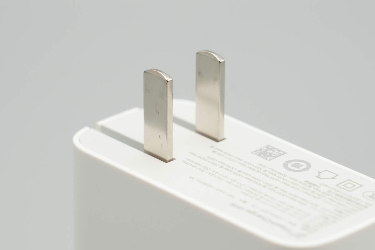
It is equipped with foldable prongs.
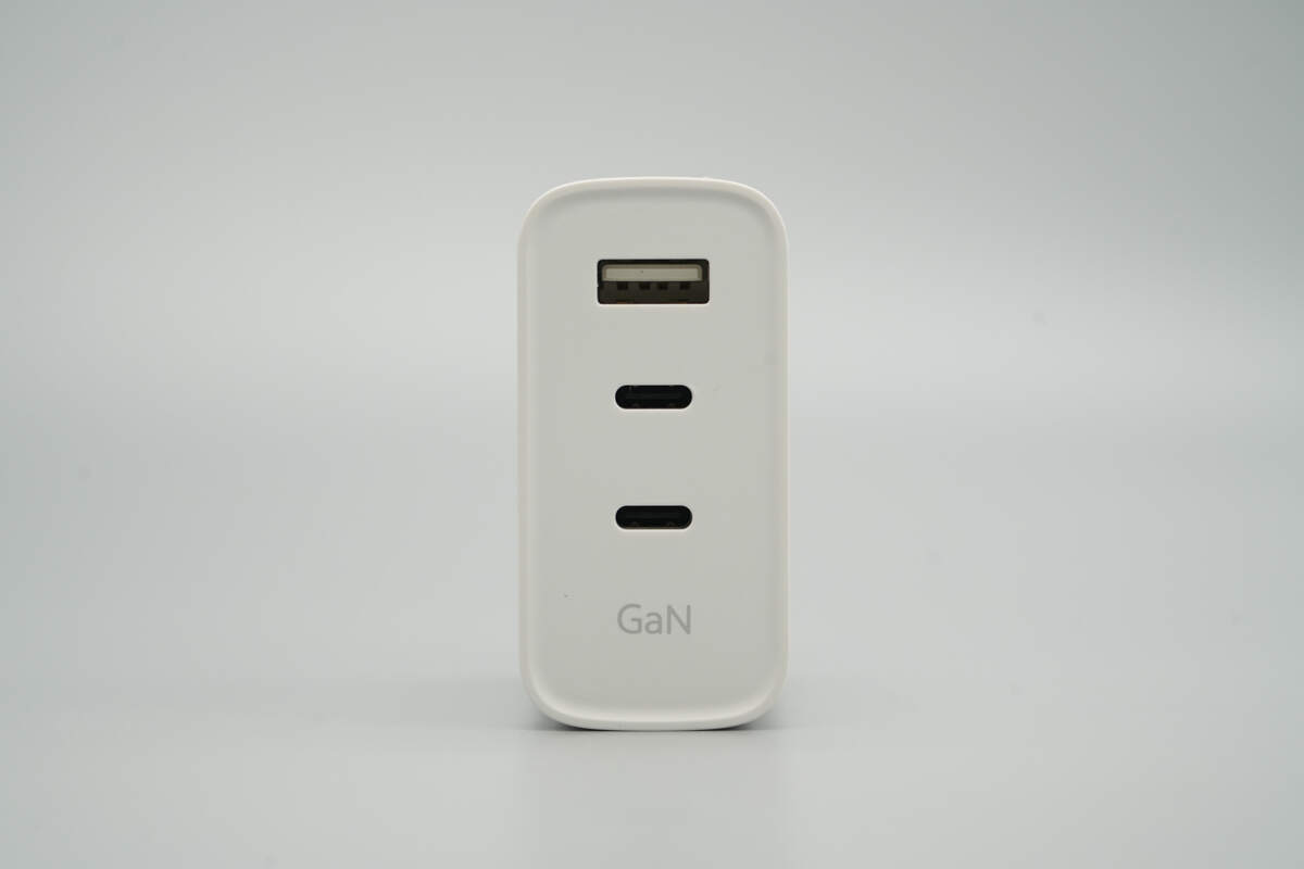
The top features three USB ports: two USB-C and one USB-A.
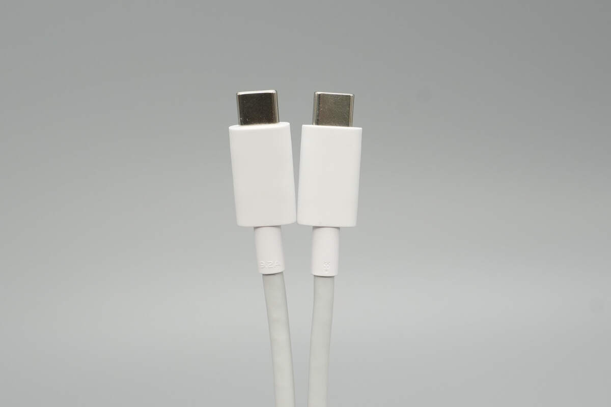
The included cable in the kit is a dual USB-C type with a current capacity of 9.2A, supporting the proprietary 11V/8.2A charging protocol.
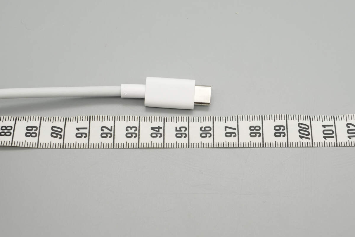
The length of the cable is about 96 cm (37.8 inches).
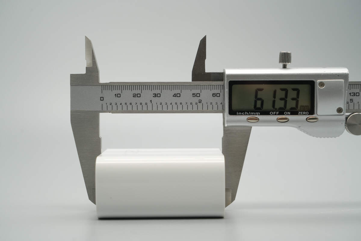
The length of the charger is about 61.33 mm (2.41 inches).
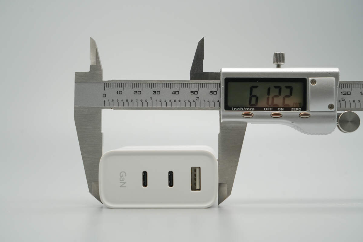
The width is about 61.22 mm (2.41 inches).
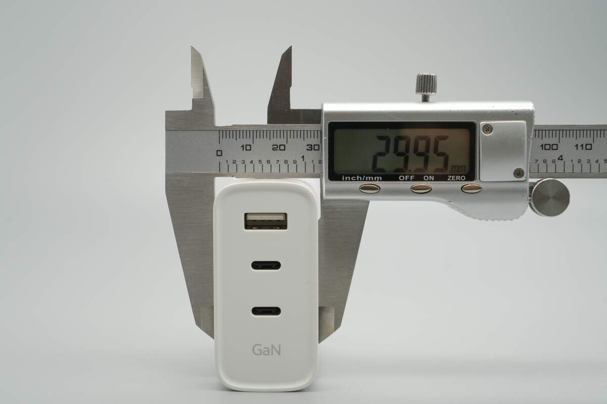
The thickness is about 29.95 mm (1.18 inches).
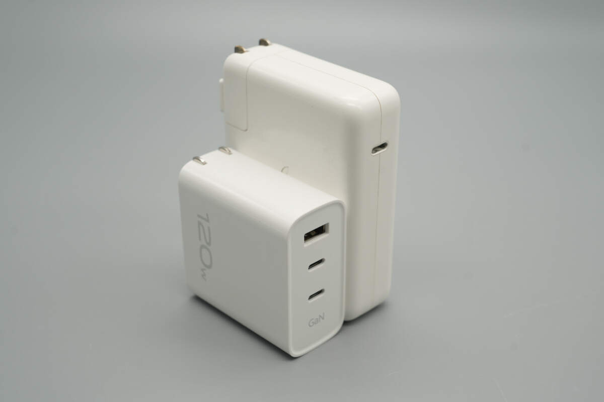
It is much smaller in size compared to Apple’s 140W GaN charger.
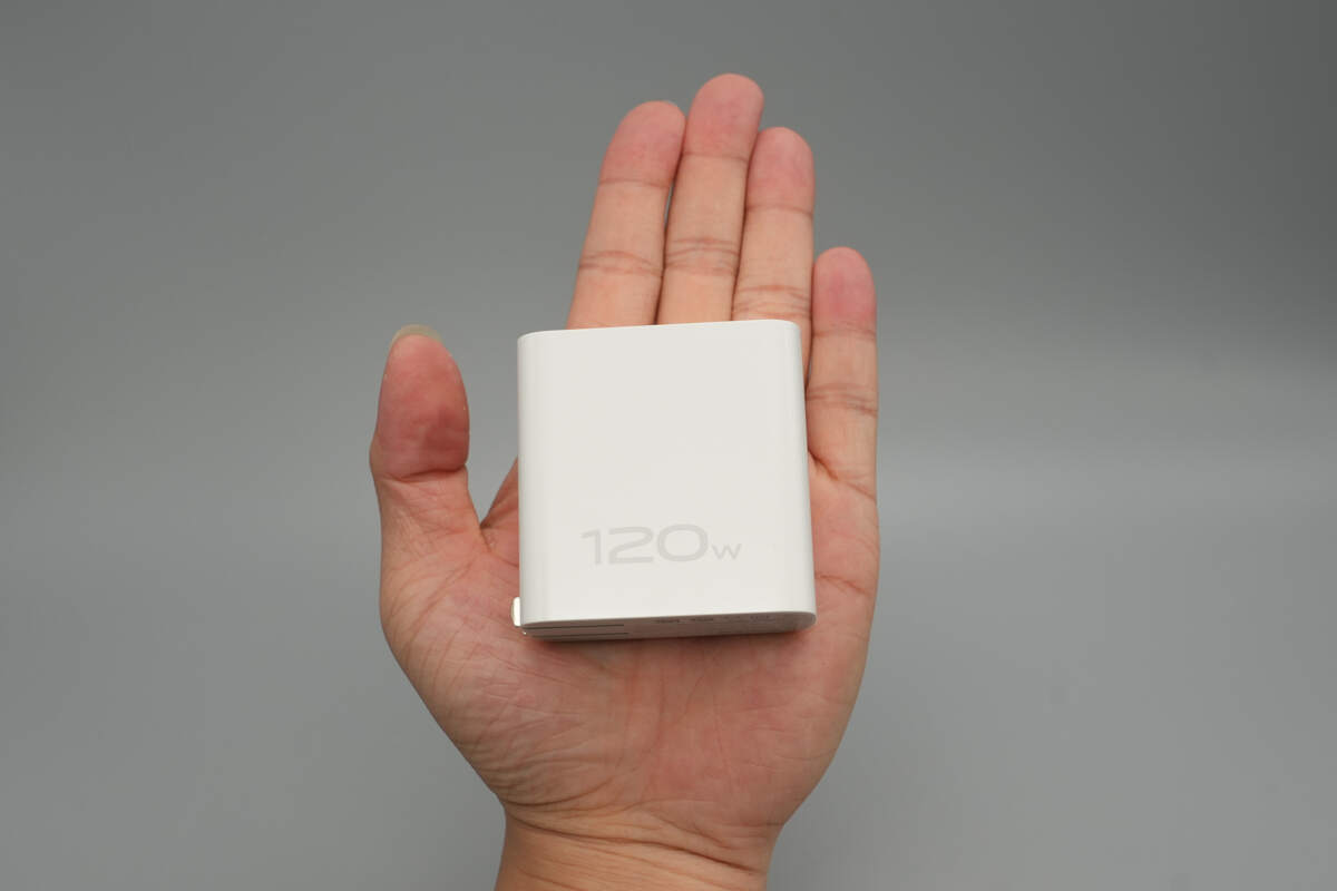
That's how big it is in the hand.
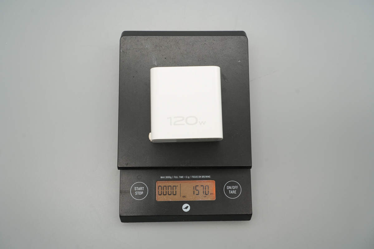
The weight is about 157 g (5.54 oz).
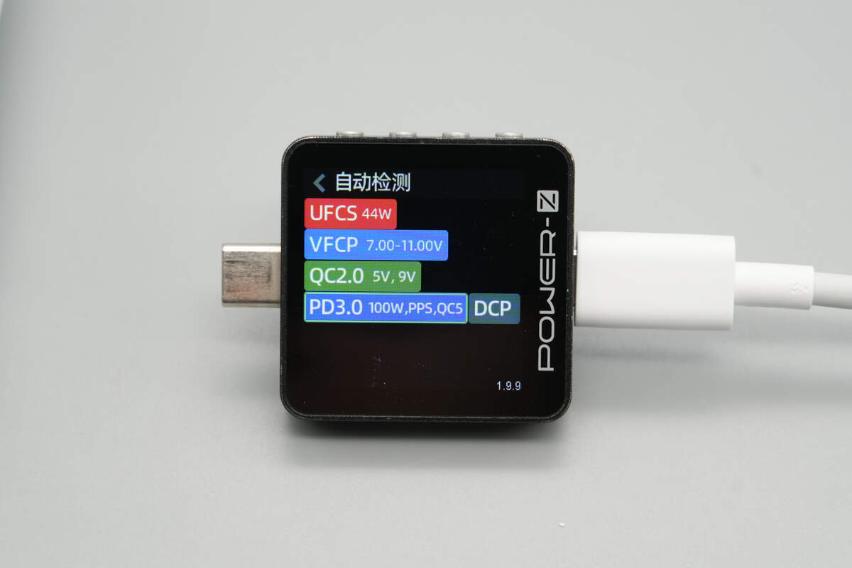
ChargerLAB POWER-Z KM003C shows that the UAB-C1 supports UFCS, VFCP, QC2.0/5, PD3.0, PPS, and DCP protocols.
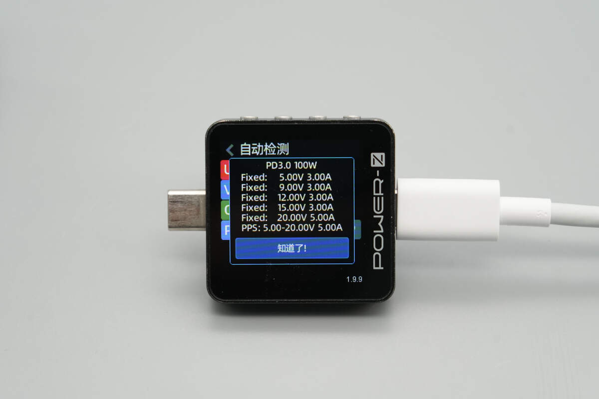
It has five fixed PDOs of 5V3A, 9V3A, 12V3A, 15V3A, and 20V5A. It also has one set of PPS, which is 5-20V5A.
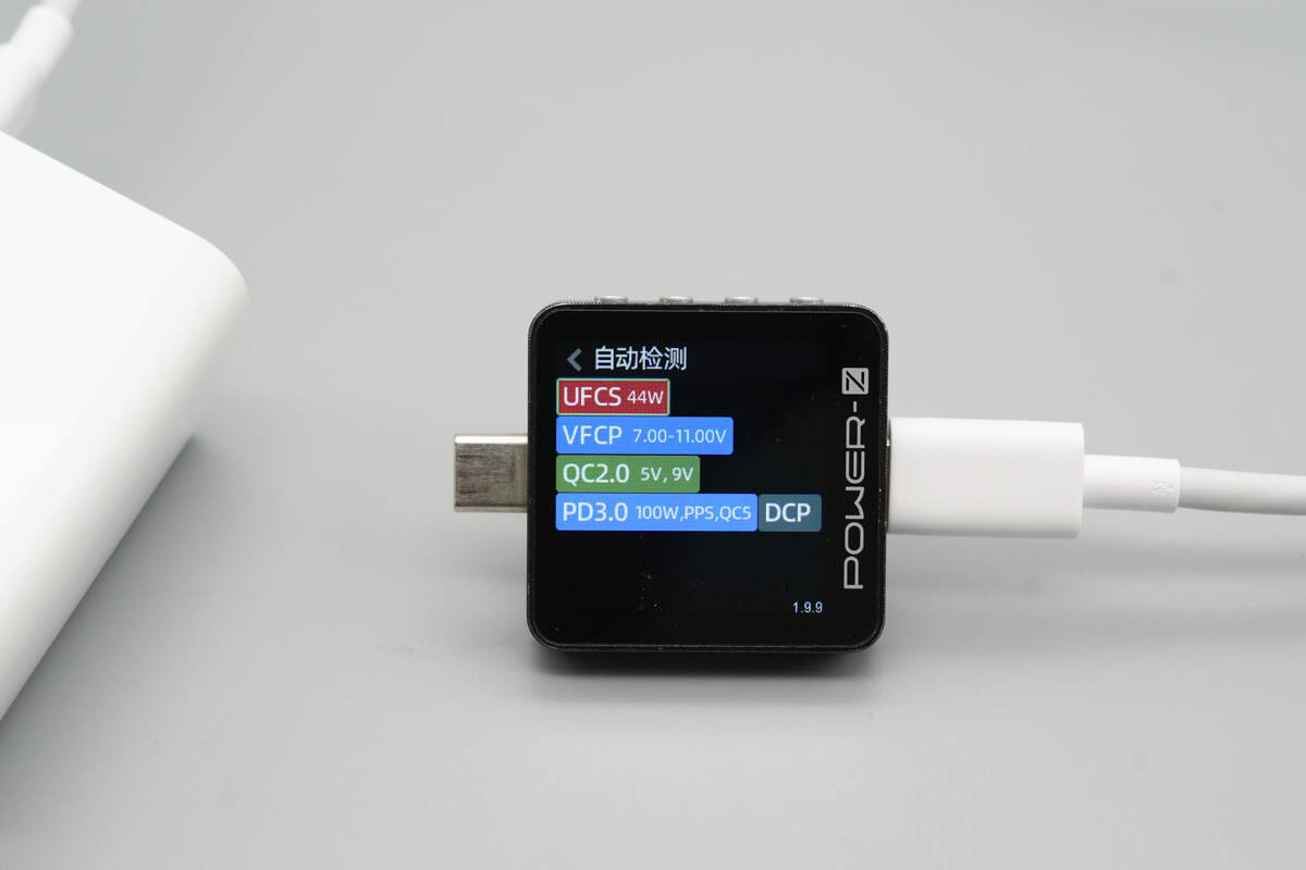
The USB-C2 port supports the same charging protocols as the USB-C1 port.

The PDO profiles are also identical between the two ports.

The USB-A port supports UFCS, VFCP, QC2.0, and DCP protocols.
Teardown
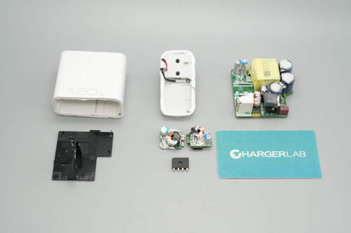
Next, let's take it apart to see its internal components and structure.
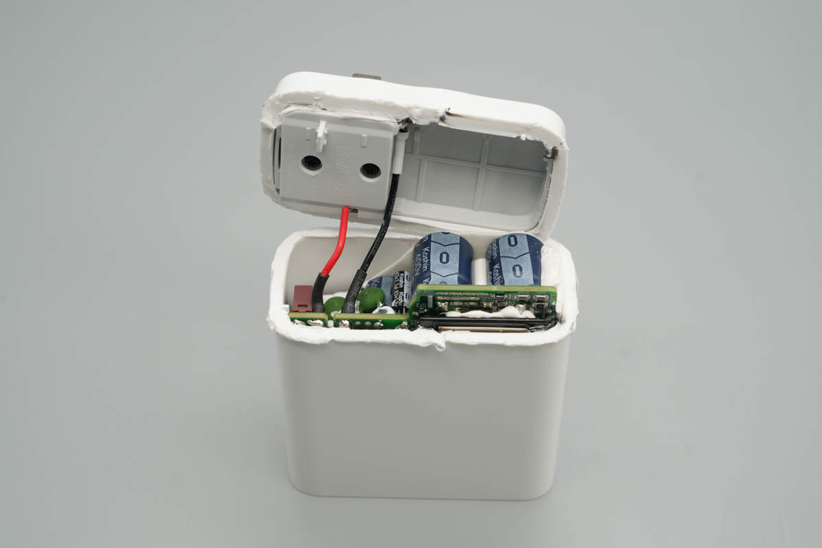
Cut open the input casing. The prongs are connected to the PCBA module via wires. Both ends of the wires are covered with insulating sleeves.
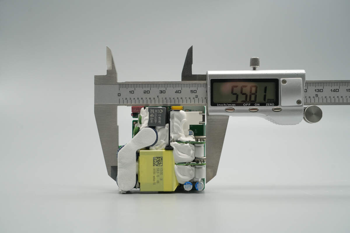
Remove the PCBA module. The length of the PCBA module is about 55.81 mm (2.2 inches).
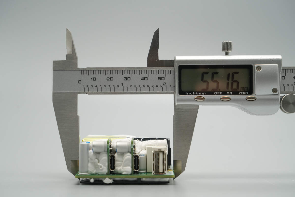
The width is about 55.18 mm (2.17 inches).
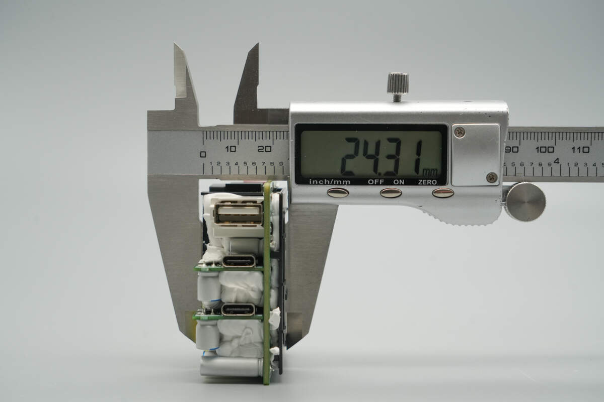
The thickness is about 24.31 mm (0.96 inches).
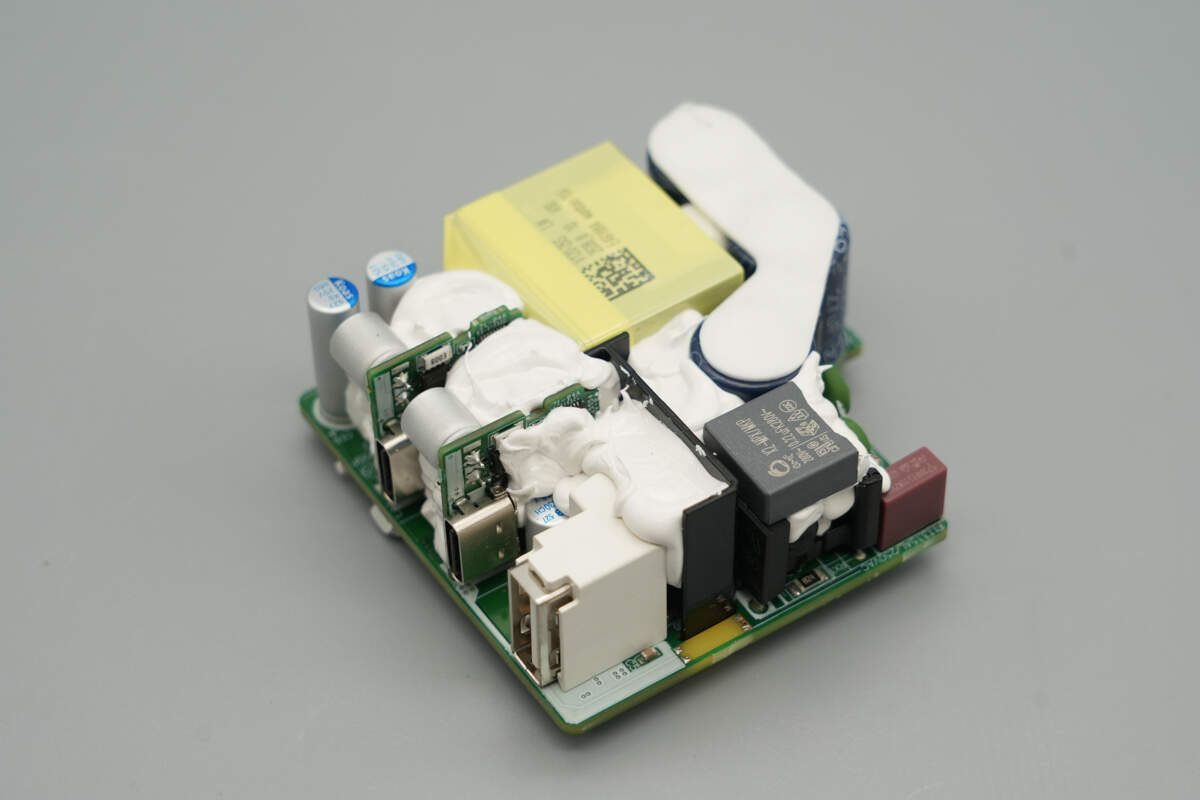
The front of the PCBA module is reinforced with adhesive. A sponge pad is attached to the top of the high-voltage filter electrolytic capacitors. A plastic separator is installed between the primary and secondary sides for isolation and insulation.
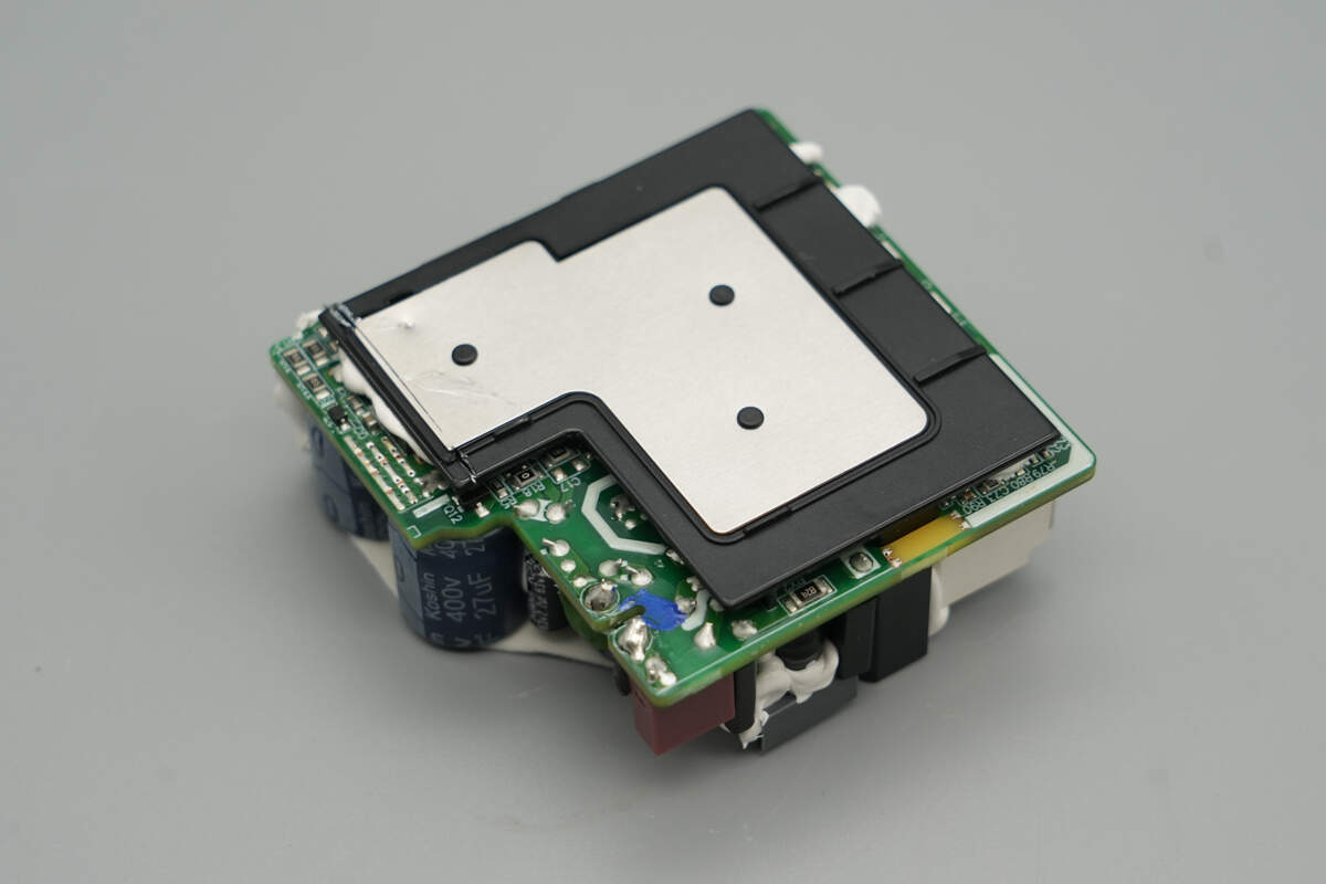
The bottom is covered by a plastic plate and a heatsink.
Clean off the adhesive. The component layout is compact.

On the back side, there are components including the master control chip, primary MOSFET, synchronous rectifier, buck converter chip for the USB-A port, and VBUS MOSFET.
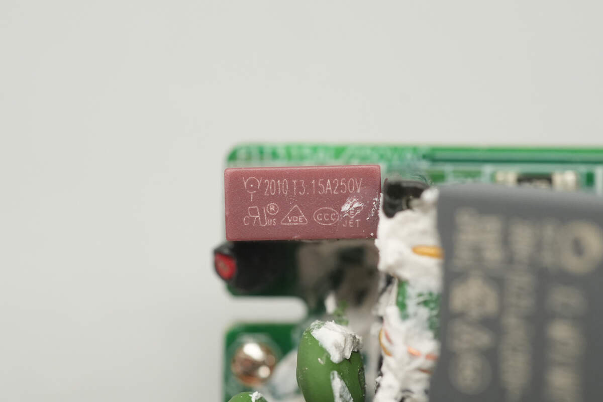
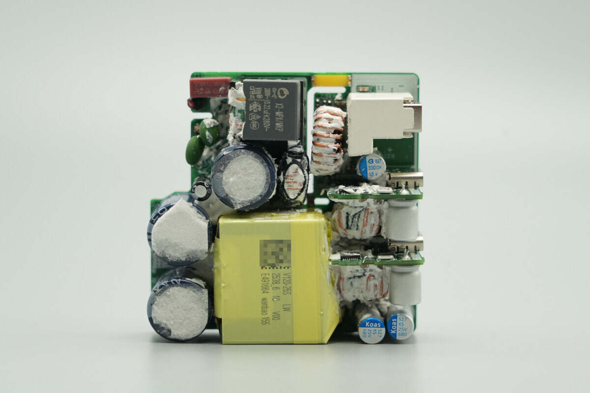
The time-delay fuse is from WalterFuse, rated at 3.15A 250V.
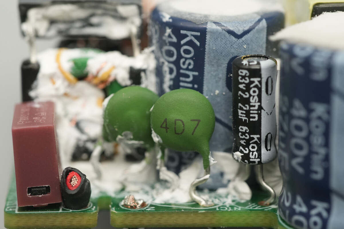
The two green NTC thermistors are used to suppress inrush current during power-up.

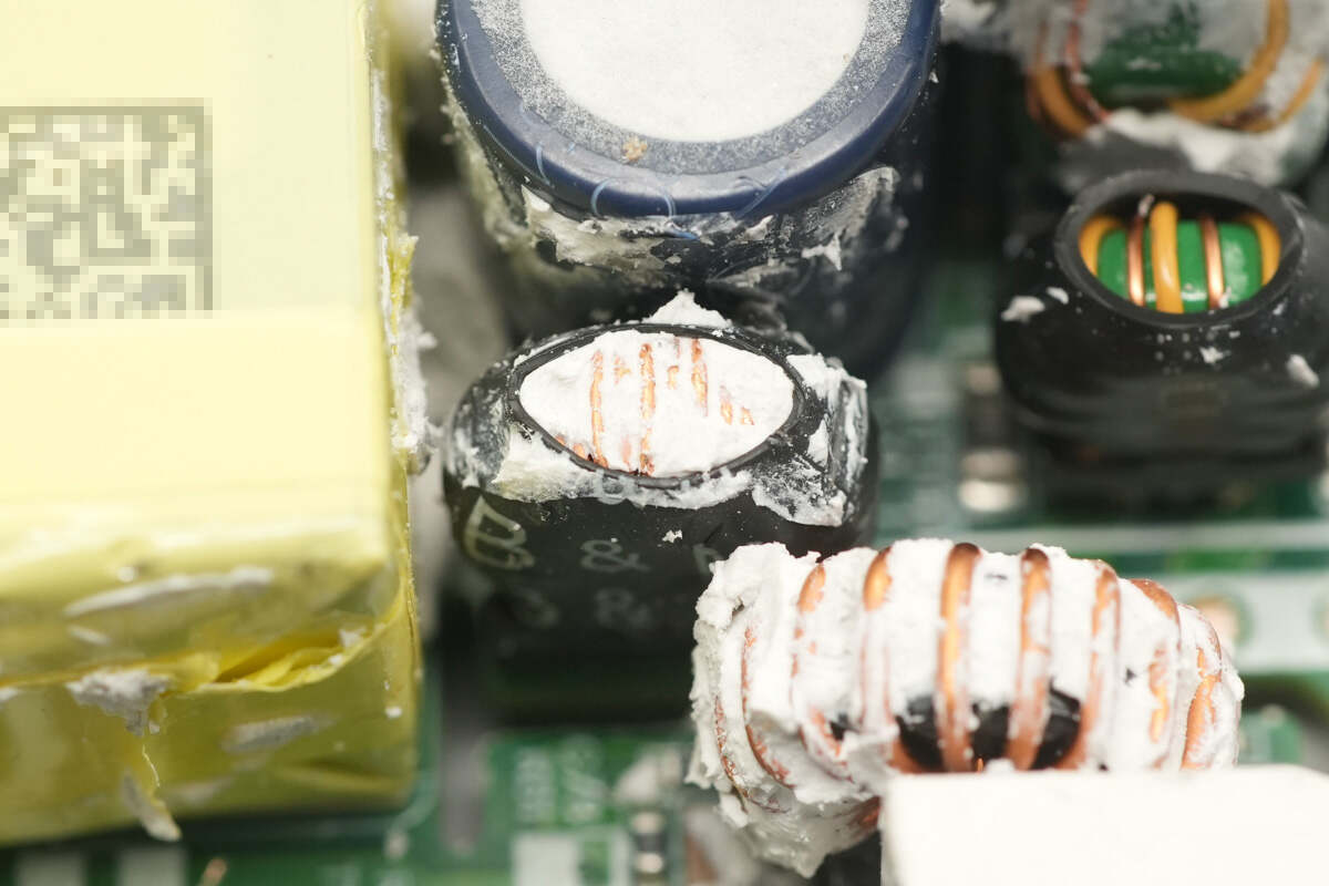
The safety X2 capacitor is soldered with an insulating sleeve. A two-stage common mode choke is designed to filter out EMI interference.
The other common mode choke is covered with a heat-shrink tube for insulation and protection.
The bridge rectifier is from Pingwei, model D8KB10A, rated at 8A 1000V, and uses a D3K package.
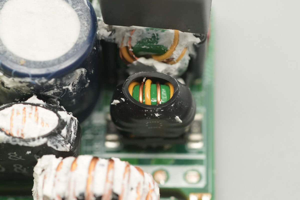
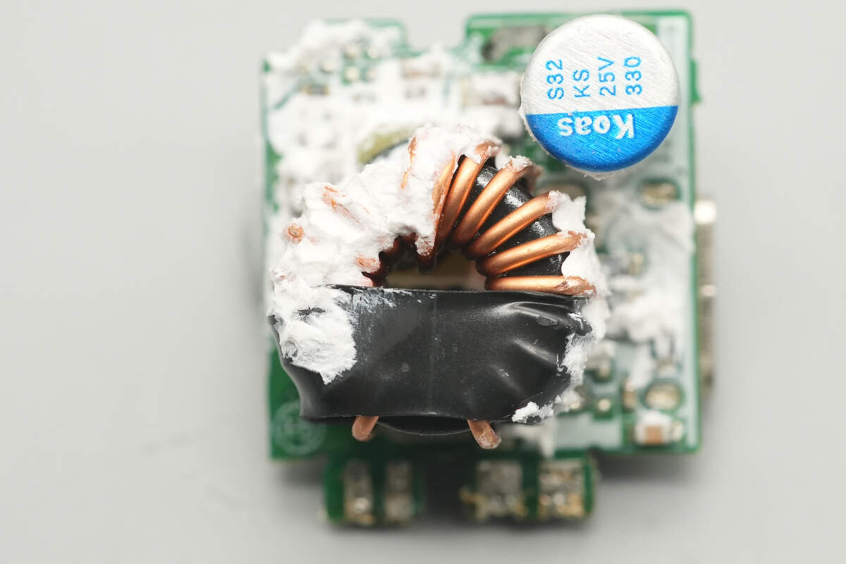
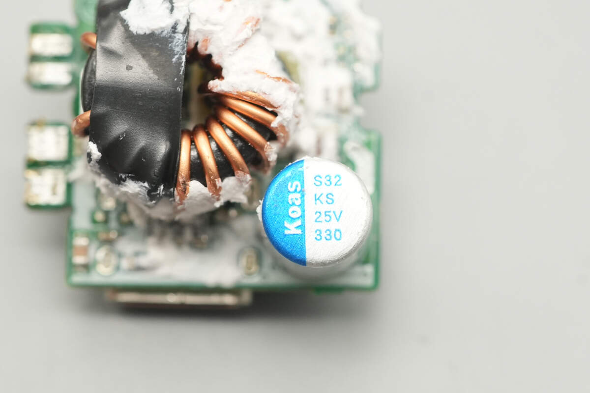
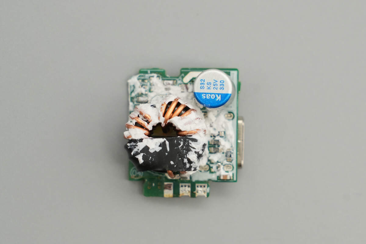
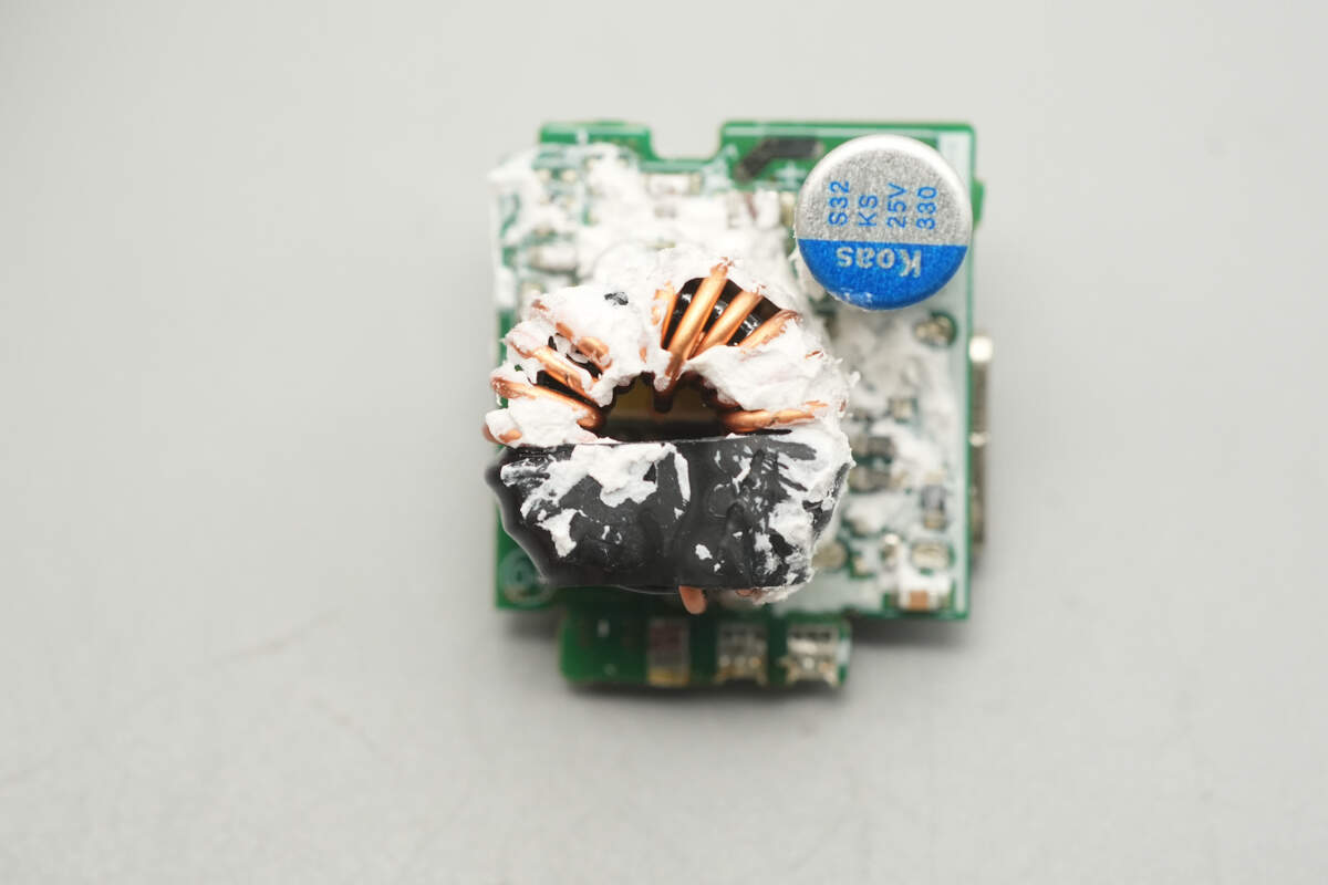
Close-up of the filter inductor.
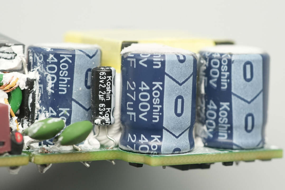
The three high-voltage filter electrolytic capacitors are from Koshin, each rated at 400V 27μF.
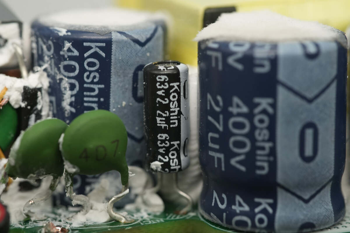
The capacitor supplying power to the master control chip is also from Koshin, rated at 63V 2.2μF.
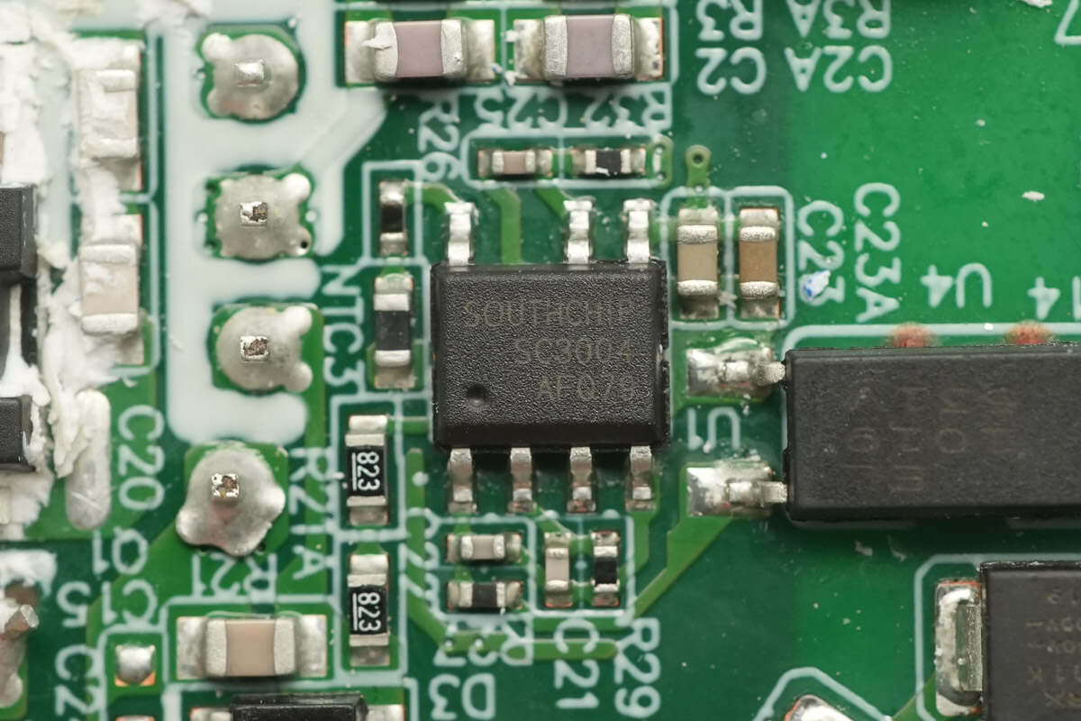
The master control chip is from SouthChip, model SC3004.
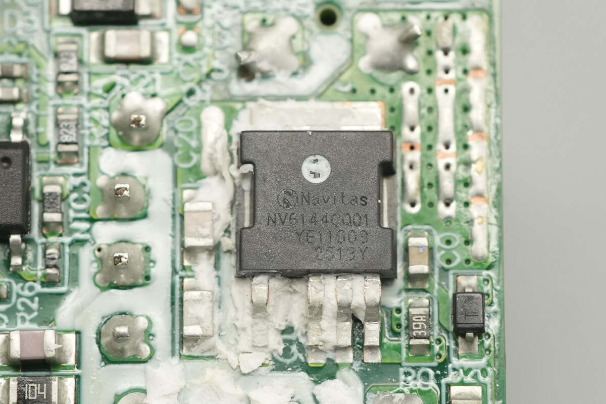
The primary MOSFET is the Navitas NV6144C, a GaNSlim GaN power chip. It integrates a 700V withstand voltage, 260mΩ high-performance enhancement-mode GaN FET, a gate driver, and extended functions, housed in a DPAK-4L package.
The device's lossless current-sensing technology eliminates the need for an external sense resistor, improving system efficiency. Overtemperature protection enhances system robustness, while automatic standby and sleep modes optimize efficiency under light, micro, and no-load conditions.
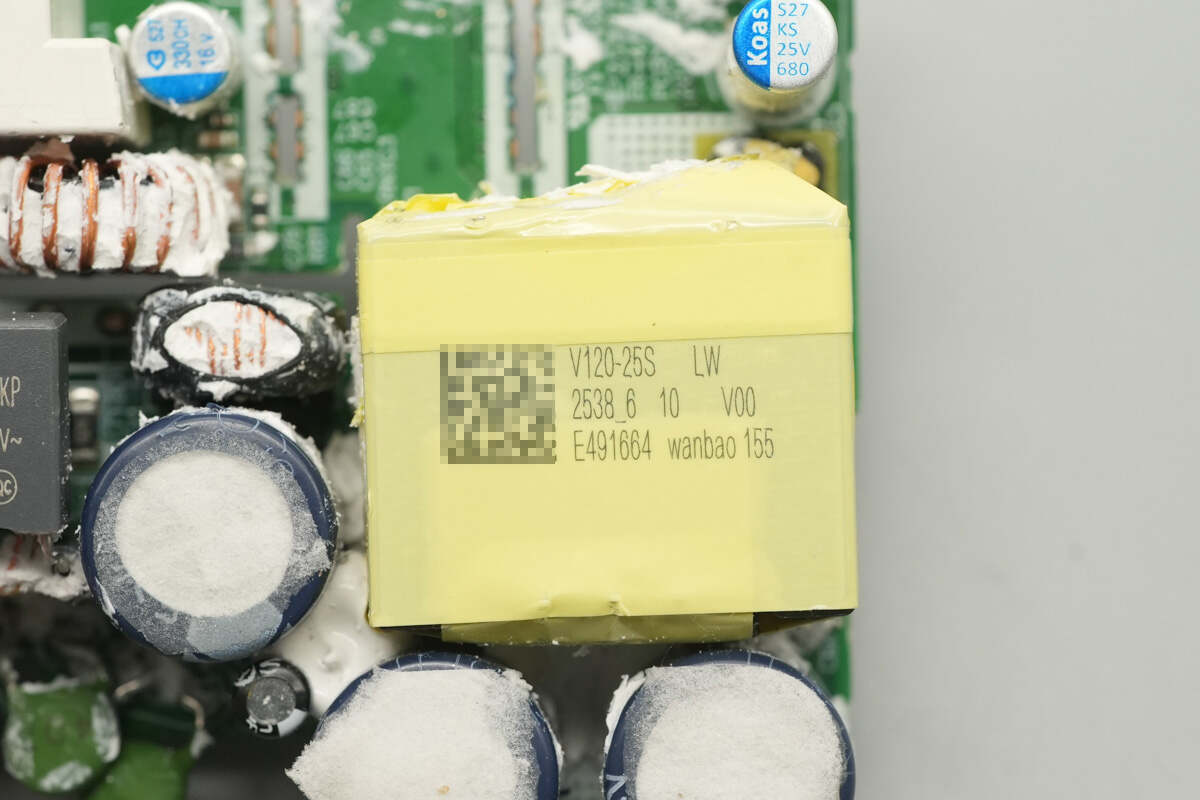
Close-up of the transformer.
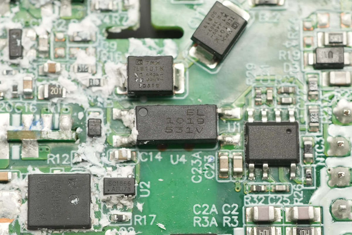
The Everlight EL1019 optocoupler is used for output voltage feedback.

The SMD Y capacitors are from TRX, model number TAY2101KB. Their small size and light weight make them well-suited for high-density power products such as GaN fast chargers.
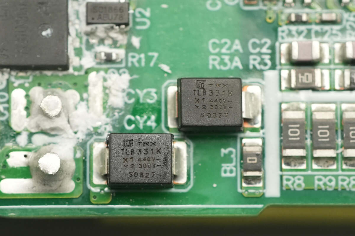
The other two TRX SMD Y capacitors have a model number of TAY2331KB.

The synchronous rectifier controller is from SouthChip, model SC1856.
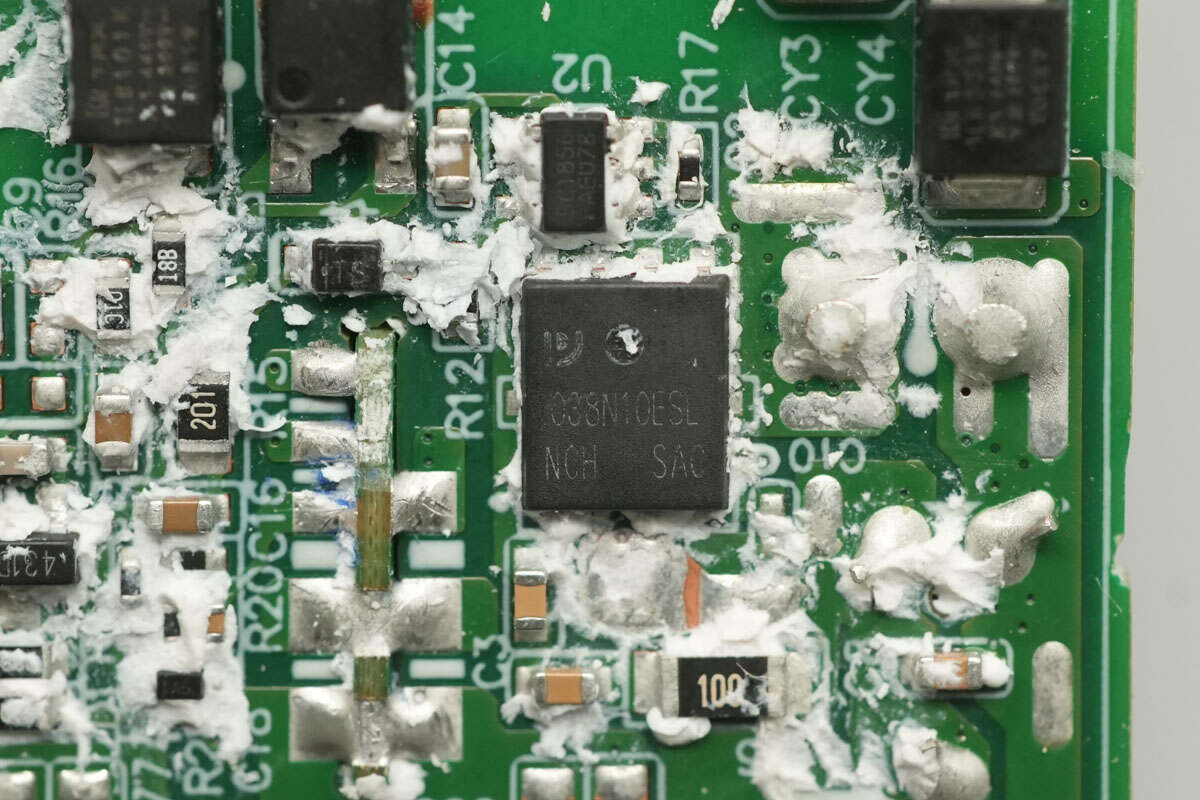
The synchronous rectifier is from Pingwei, model PW038N10ESL. It is an N-channel MOSFET with a voltage rating of 100V, an on-resistance of 3.2mΩ, and comes in a DFN 5×6 package.
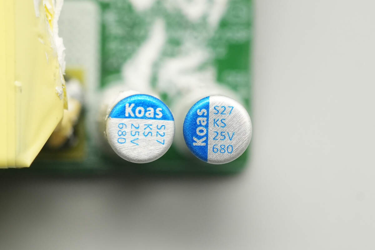
The two solid capacitors for output filtering are also from Koshin, each rated at 25V 680μF.
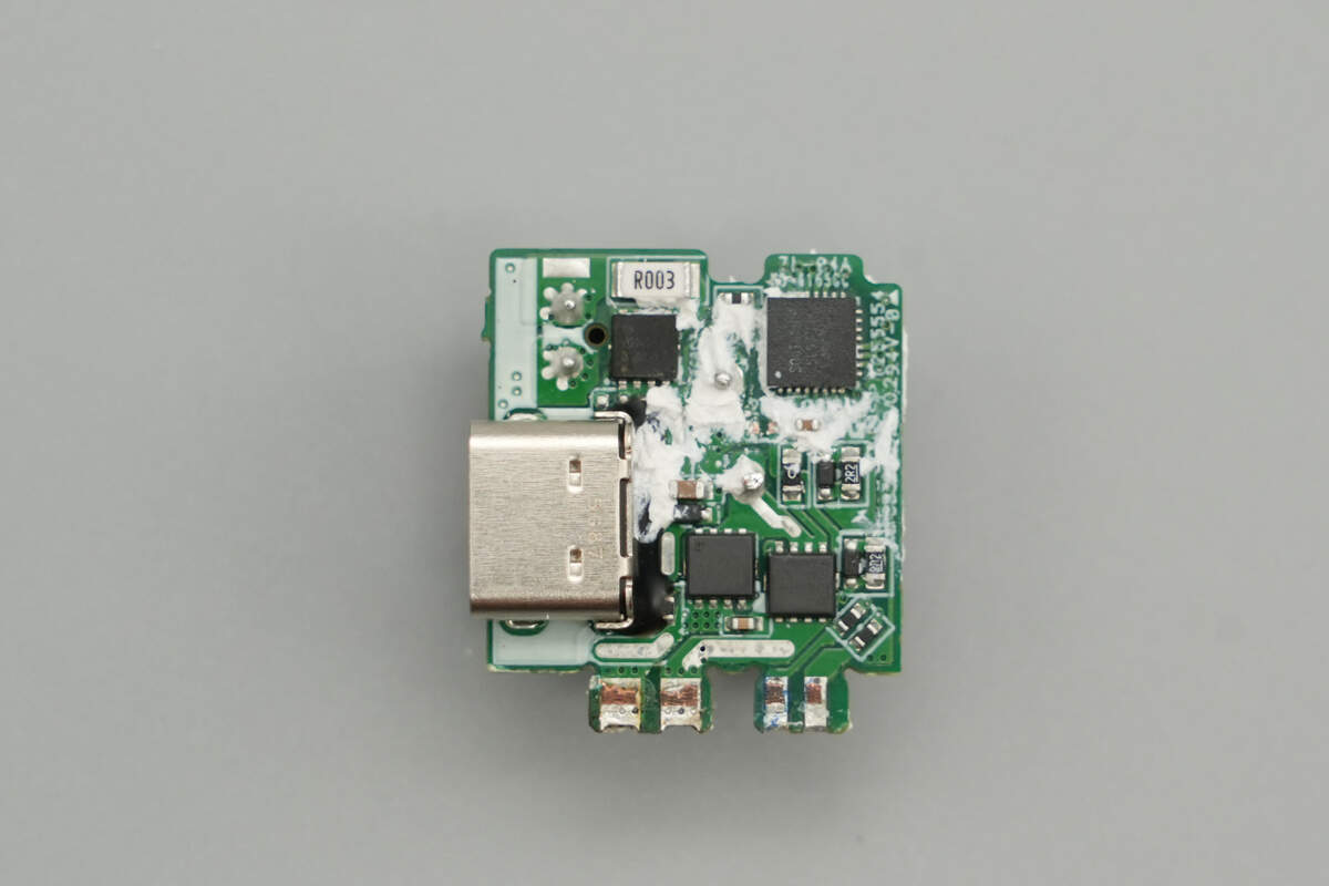
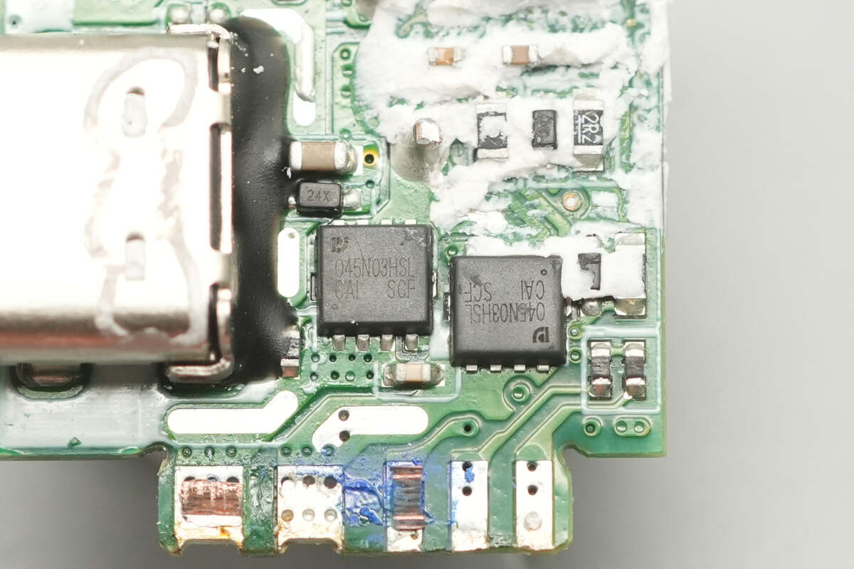
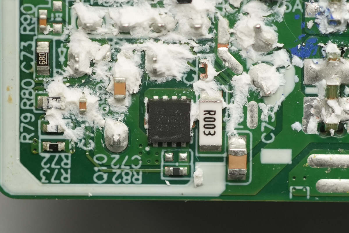
Remove all the small PCBs. On the front side of the USB-C1 PCB, there is a buck protocol chip, synchronous buck MOSFETs, and a VBUS MOSFET.
The other side is equipped with a buck inductor and a solid capacitor.
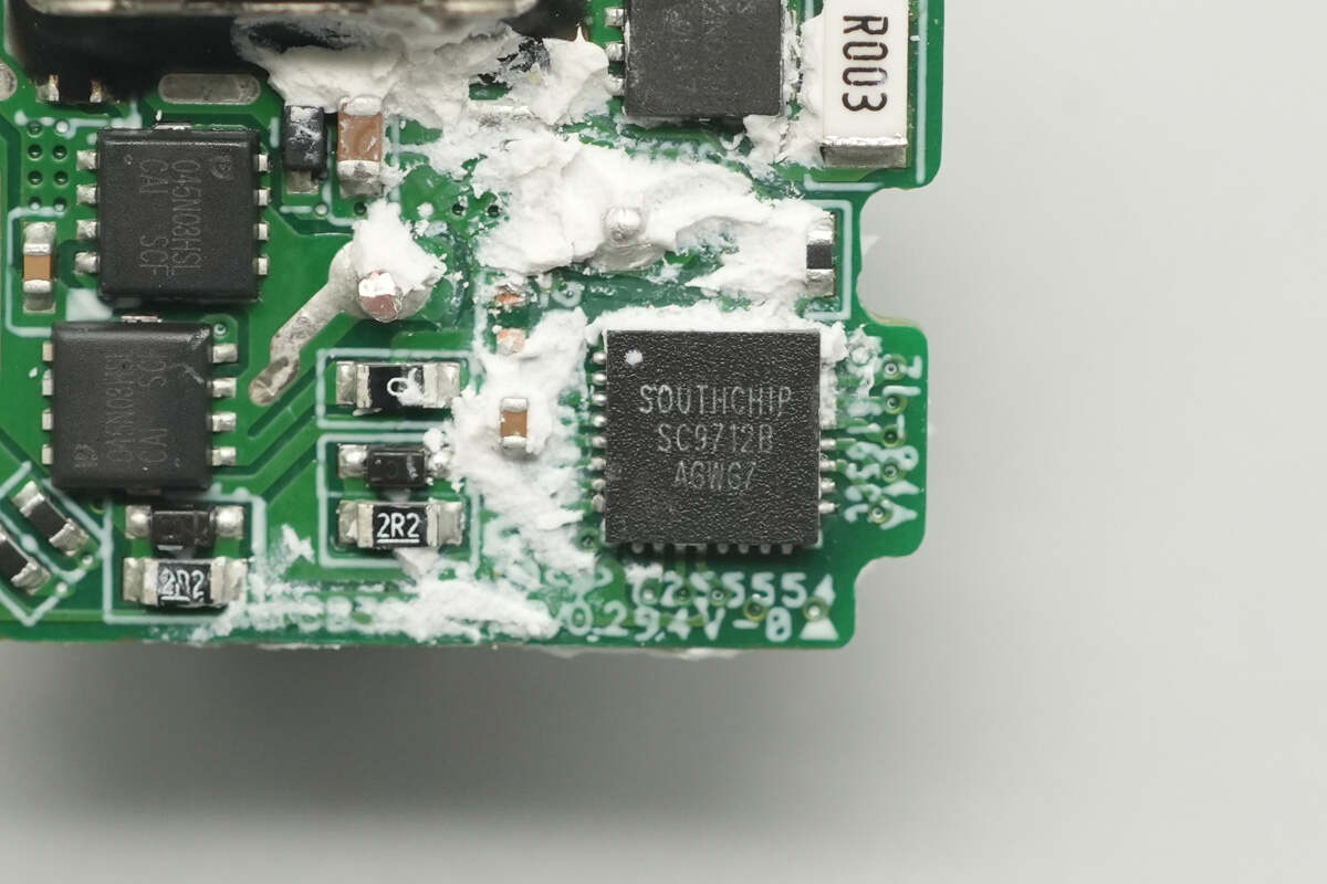
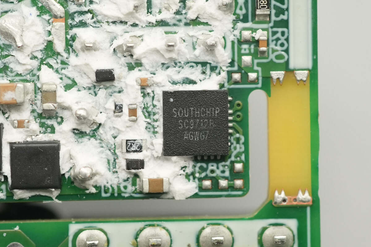
The buck protocol chip is from SouthChip, model SC9712B. It is a highly integrated dual-port fast charging SoC that supports multiple fast charging protocols. It integrates a 36V high-efficiency synchronous buck controller and includes one Type-C interface along with two sets of DPDM quick charging protocol interfaces, minimizing the need for external components.
The SC9712B supports dual-chip cooperative operation to enable fast charging on two USB-C ports. The configuration of two USB-C ports and one USB-A port requires no MCU control. The two SC9712B chips communicate with each other to deliver full power output when operating a single port and automatically allocate power when both ports are in use simultaneously.

The SC9712B supports a total output power of up to 140W. Both dual-port outputs fully support CC/CV mode and feature NTC temperature monitoring. It provides multiple protection mechanisms, including overvoltage protection, overcurrent protection, short-circuit protection, and overtemperature protection, effectively safeguarding the chip and the system. The chip comes in a 32-pin, 4×4mm QFN package.
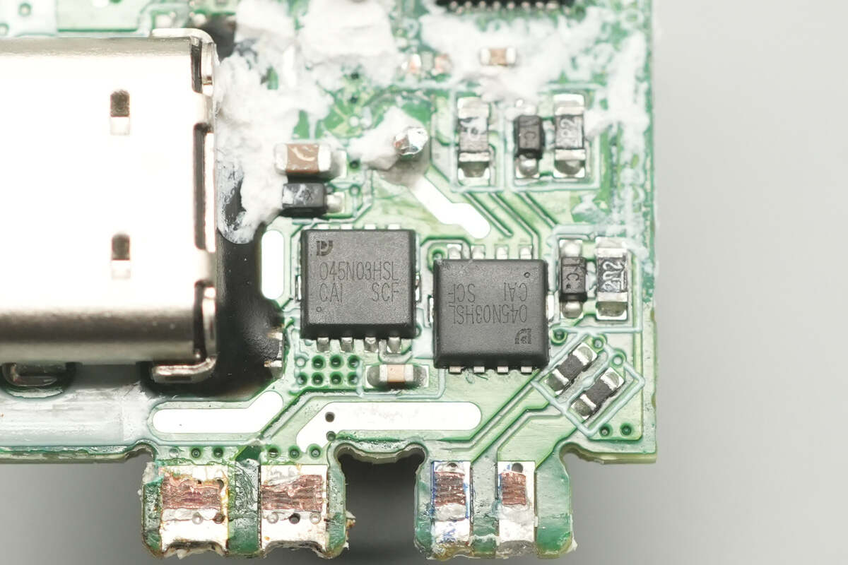
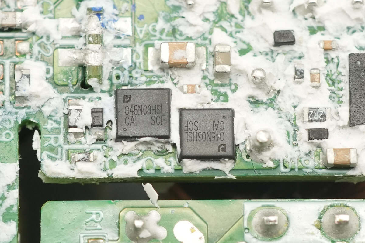
The synchronous buck MOSFETs are from Pingwei, model PW045N03HSL. They are N-channel MOSFETs with a voltage rating of 30V, an on-resistance of 3.8mΩ, and come in a DFN 3×3 package.
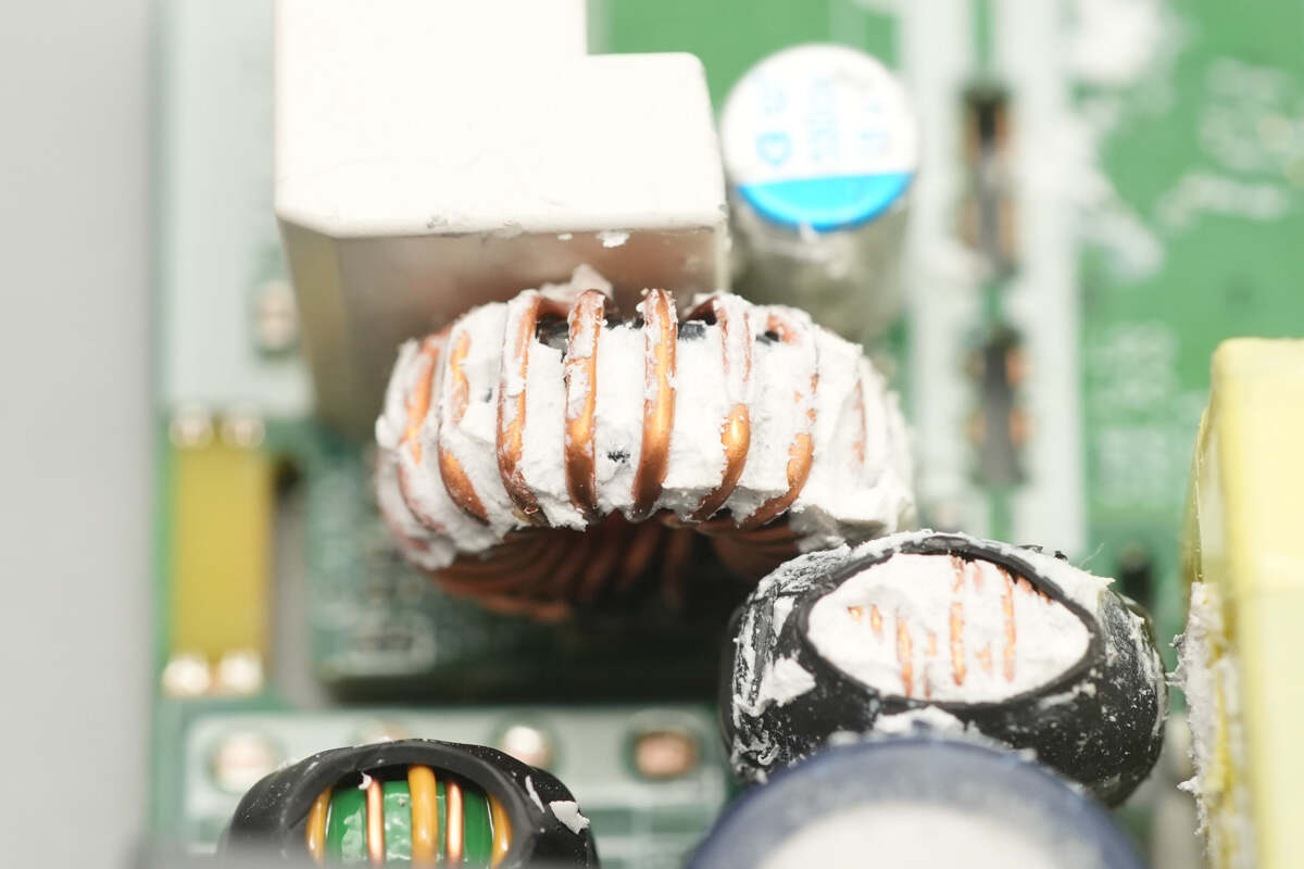
Close-up of the buck inductor.
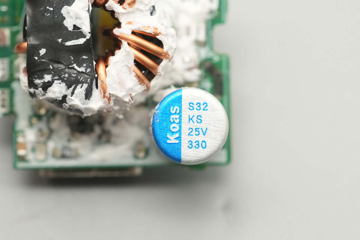
The solid capacitor is also from Koshin, rated at 25V 330μF.
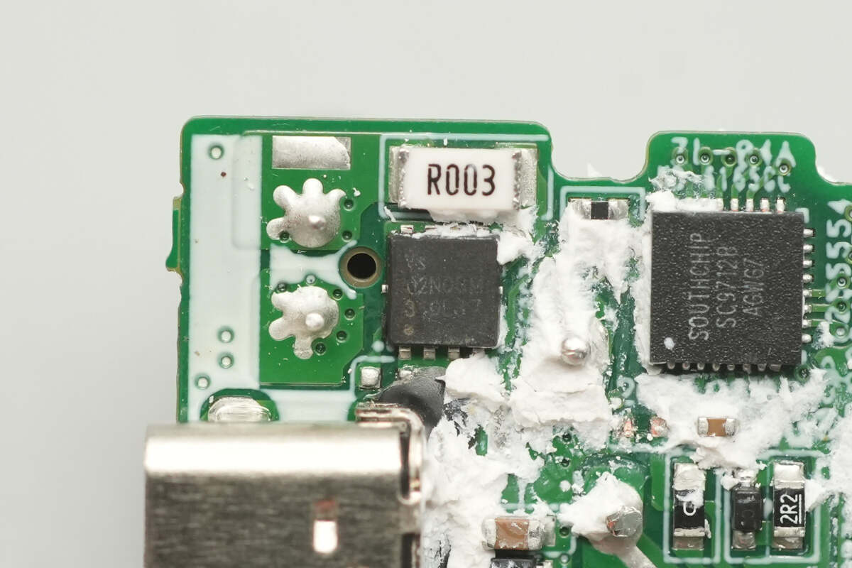
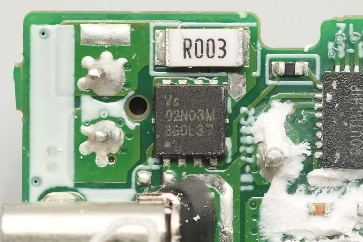
The VBUS MOSFET is from Vergiga, model VSE002N03MS-G. It is an N-channel MOSFET with a voltage rating of 30V, an on-resistance of 1.4mΩ, and comes in a PDFN 3×3×3 package.
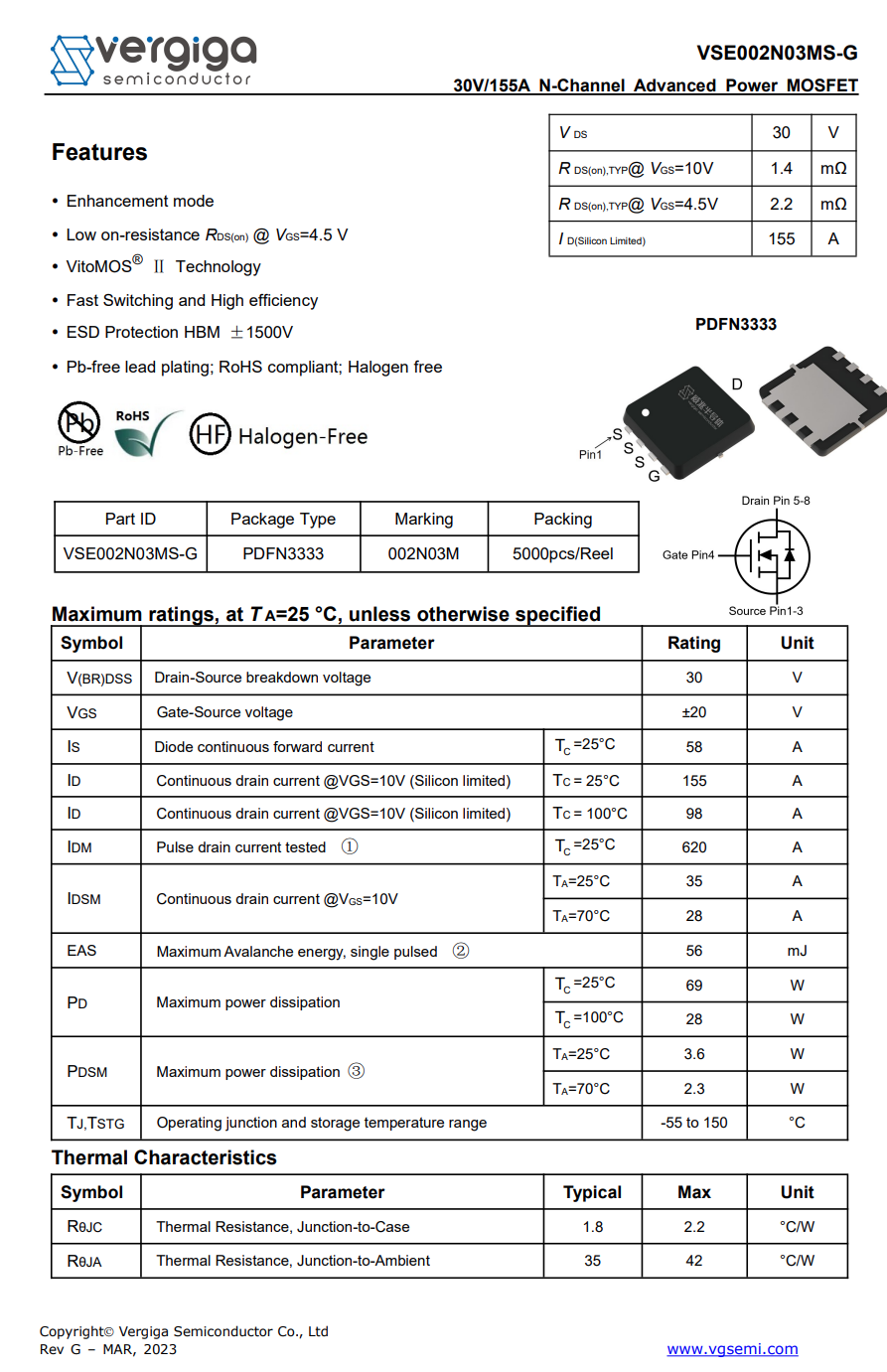
Here is the information about the Vergiga VSE002N03MS-G.

The front side of the USB-C2 PCB also features a buck protocol chip, synchronous buck MOSFETs, and a VBUS MOSFET.
On the back side, there is one buck inductor and one solid capacitor. Both small PCBs are identical in design and components.

The buck protocol chip for the USB-C2 port is also a SouthChip SC9712B.
The synchronous buck MOSFETs used are Pingwei PW045N03HSL.
The VBUS MOSFET is also Vergiga VSE002N03MS-G.
Close-up of the buck inductor.
The solid capacitor is also from Koshin, with the same specifications.
The USB-A port buck protocol chip also uses SouthChip SC9712B.
The synchronous buck MOSFETs also use Pingwei PW045N03HSL.
Close-up of the buck inductor.
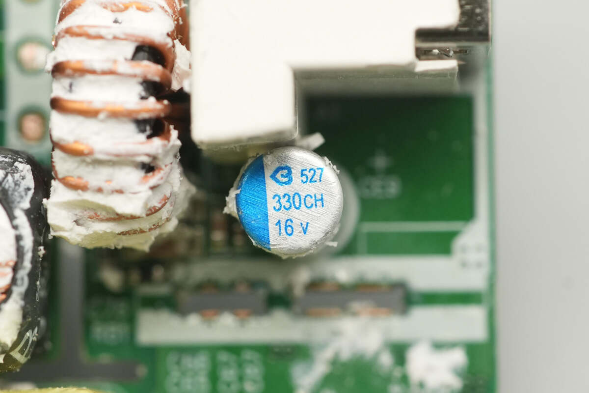
The solid capacitor is from BERYL, rated at 16V 330μF.
The VBUS MOSFET is also Vergiga VSE002N03MS-G.

Well, those are all components of the vivo 120W Multi-Port GaN Charger.
Summary of ChargerLAB
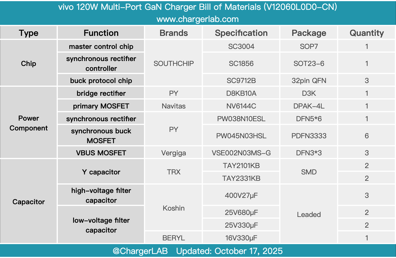
Here is the component list of the vivo 120W Multi-Port GaN Charger for your convenience.
It features two USB-C ports and one USB-A port. It supports vivo's proprietary charging protocol and is also compatible with 44W UFCS, 100W PD fast charging, and a 5–20V 5A PPS fast charging profile.
After taking it apart, we found that it is based on the SouthChip SC3004 and SC1856 high-frequency QR power design, utilizing the Navitas NV6144C GaN device and Pingwei synchronous rectifier. All three output DC-DC secondary buck circuits use the SouthChip SC9712B. The electrolytic and solid capacitors are from Koshin, with components reinforced by adhesive, ensuring reliable workmanship.
Related Articles:
1. Teardown of Xiaomi 30W 2-in-1 Magnetic Wireless Charger (MDY-20-EC)
2. Teardown of Xiaomi 30W Car Magnetic Wireless Charger (MDY-20-ED)
3. Teardown of Boco Electronics 800W SiC Server Power Supply (BCSE800AP-12E01)