Introduction
UGREEN has launched a new Thunderbolt 5 docking station featuring an external power supply. It includes one Thunderbolt 5 upstream port and three Thunderbolt 5 downstream ports. Powered by Intel's JHL9480 Thunderbolt controller, it supports data transfer speeds of up to 120Gbps and 140W fast charging. The Thunderbolt 5 downstream ports allow for monitor expansion, supporting dual 8K 60Hz or dual 4K 240Hz video output. Additionally, the dock is equipped with both TF and SD card slots, a 2.5G Ethernet port, and four USB-A ports for comprehensive connectivity.
The dock features an aluminum alloy casing with internal aluminum heatsinks and shielding, along with thermal pads placed over heat-generating components for efficient cooling. Non-slip pads are located on the bottom and sides, allowing for either vertical or horizontal placement. The front panel includes a power switch and status indicator lights for easy monitoring of power and connection status. Next, let’s take it apart to examine its internal components and structure.
Product Appearance
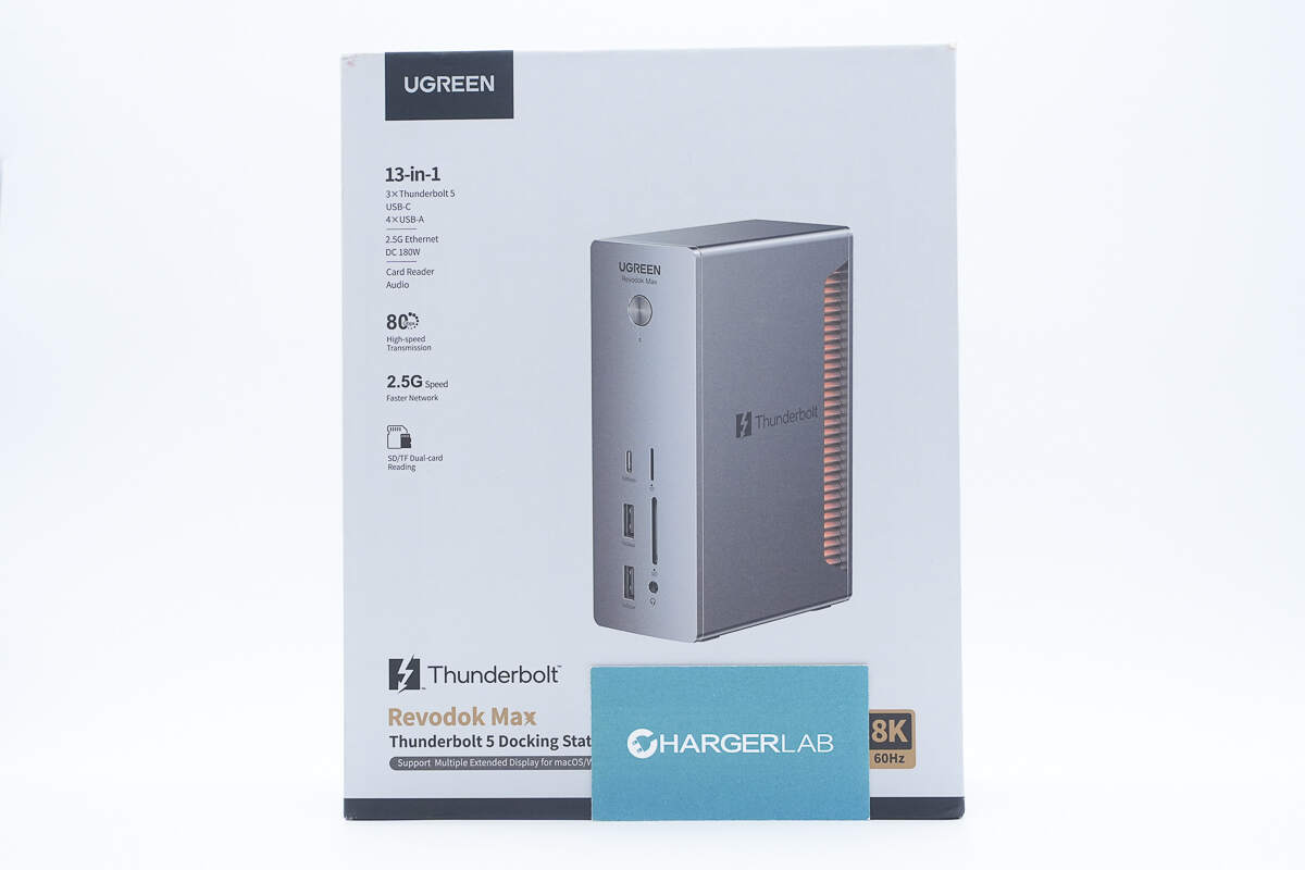
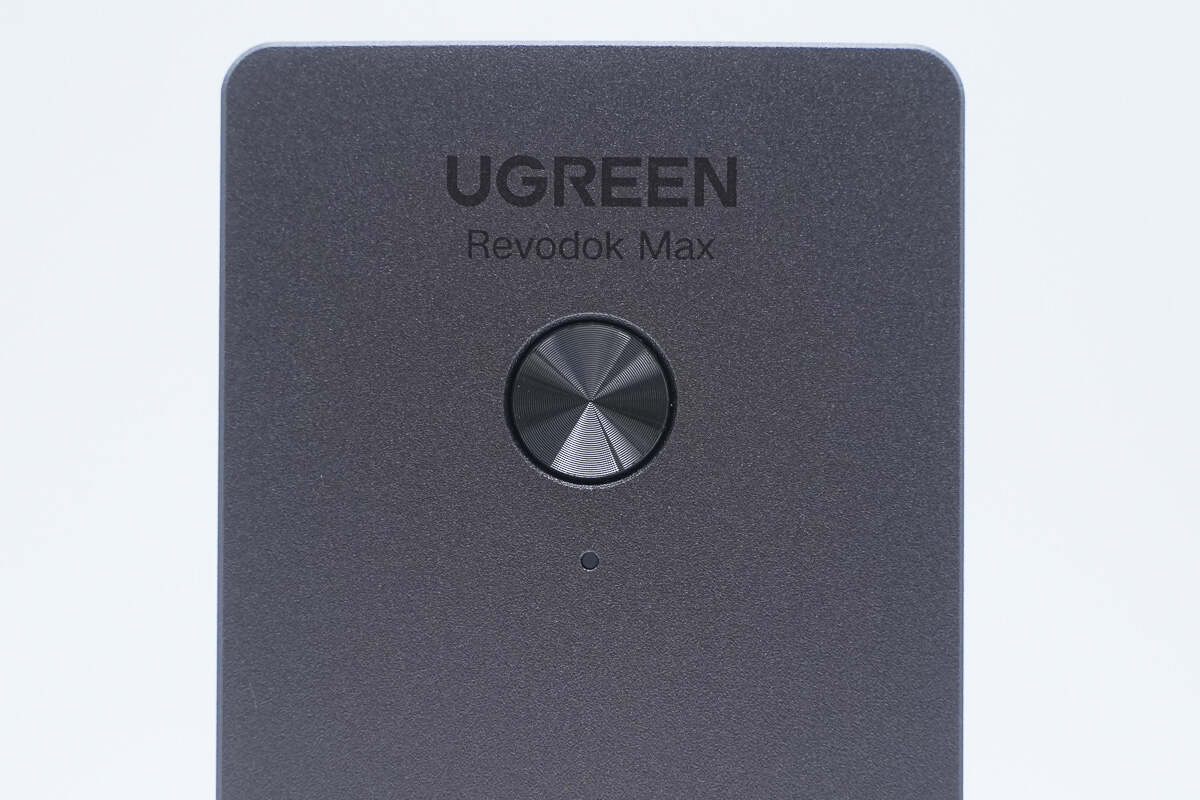
The front is printed with UGREEN, showcasing the docking station’s appearance, name, and selling points.
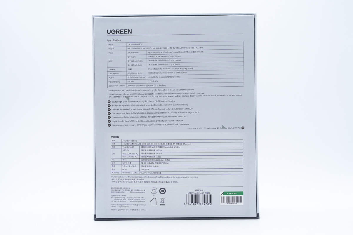
The spec info is printed on the back.
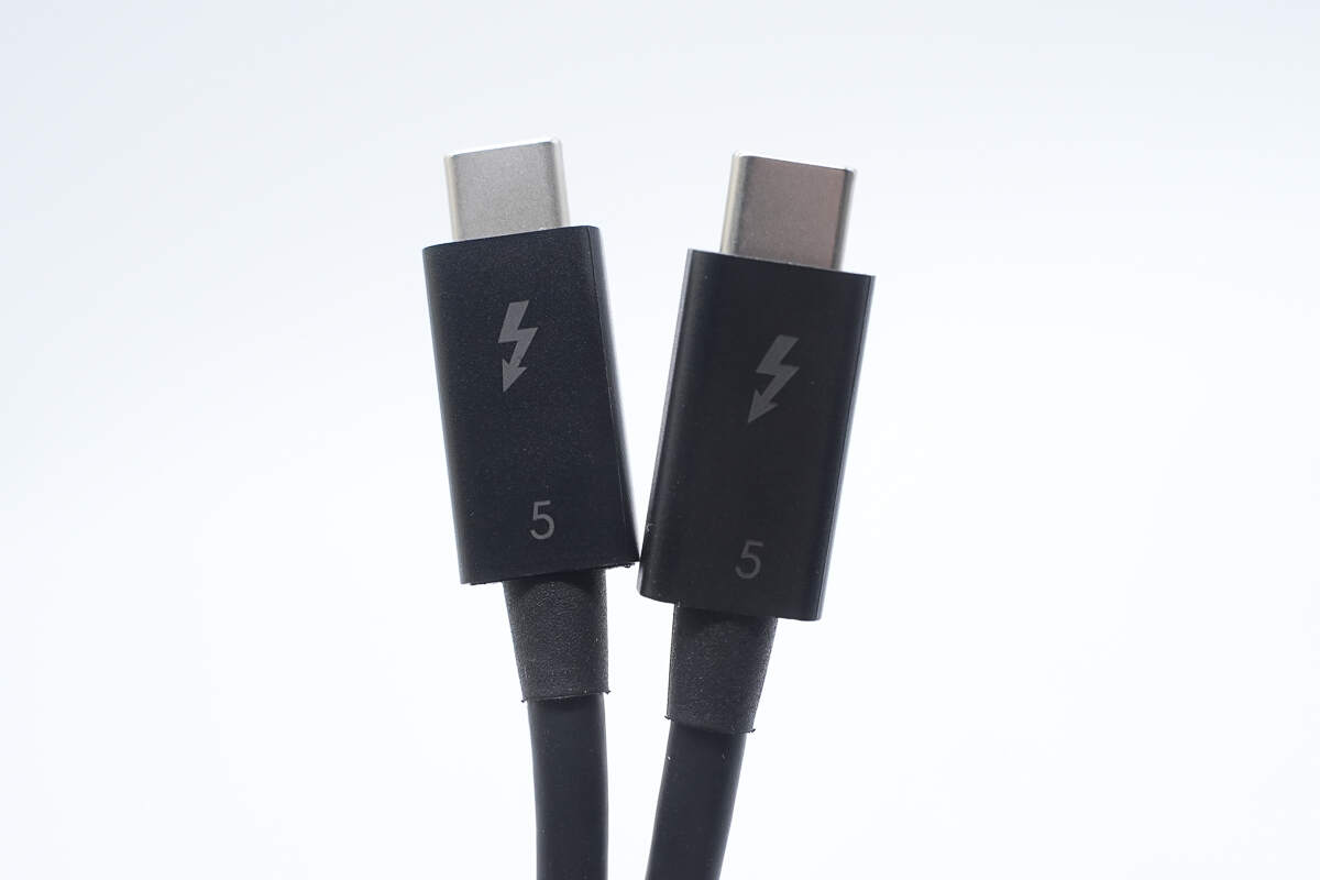
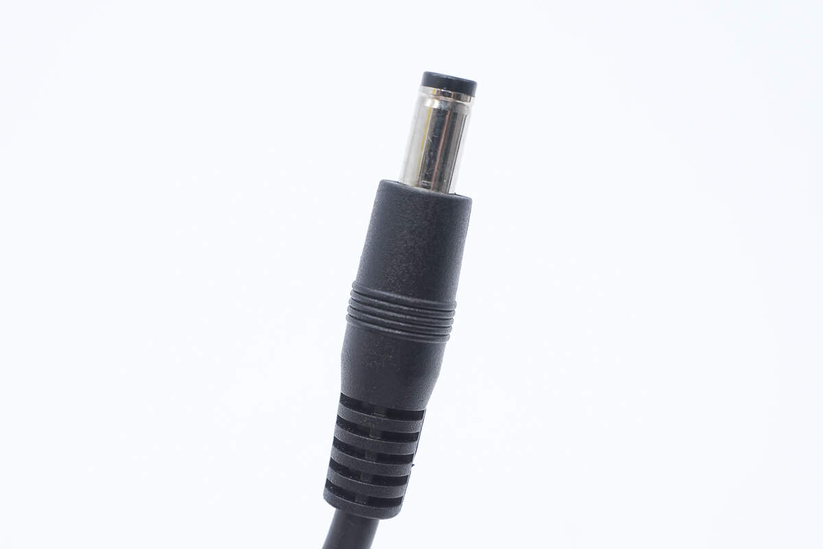
Close-up of the included Thunderbolt 5 cable's connectors.
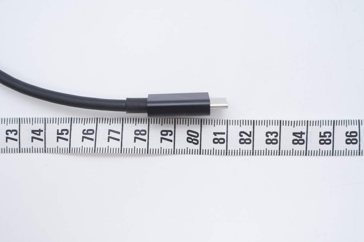
The length of the cable is about 81 cm (31.89 inches).
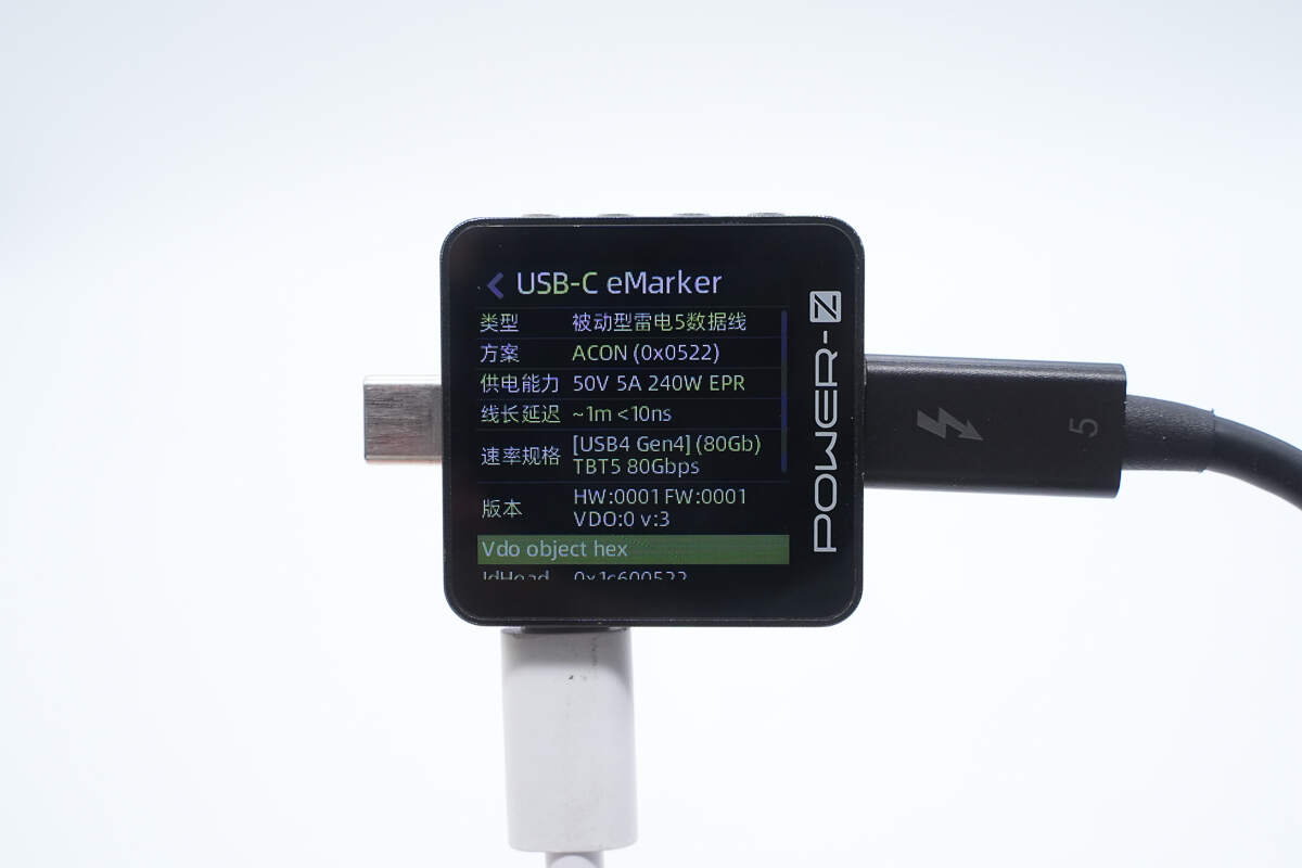
ChargerLAB POWER-Z KM003C shows it has an E-Marker chip, with a power delivery capability of 50V 5A and data transfer capability of USB4 Gen4 (80Gbps) / Thunderbolt 5 80Gbps.
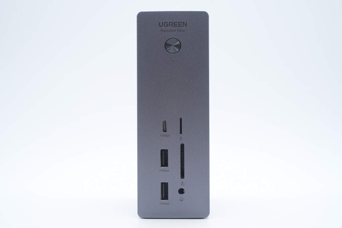
The front of the docking station features a power button, indicator light, USB ports, a TF card slot, an SD card slot, and a 3.5mm audio jack.
The indicator light is located below the power button.
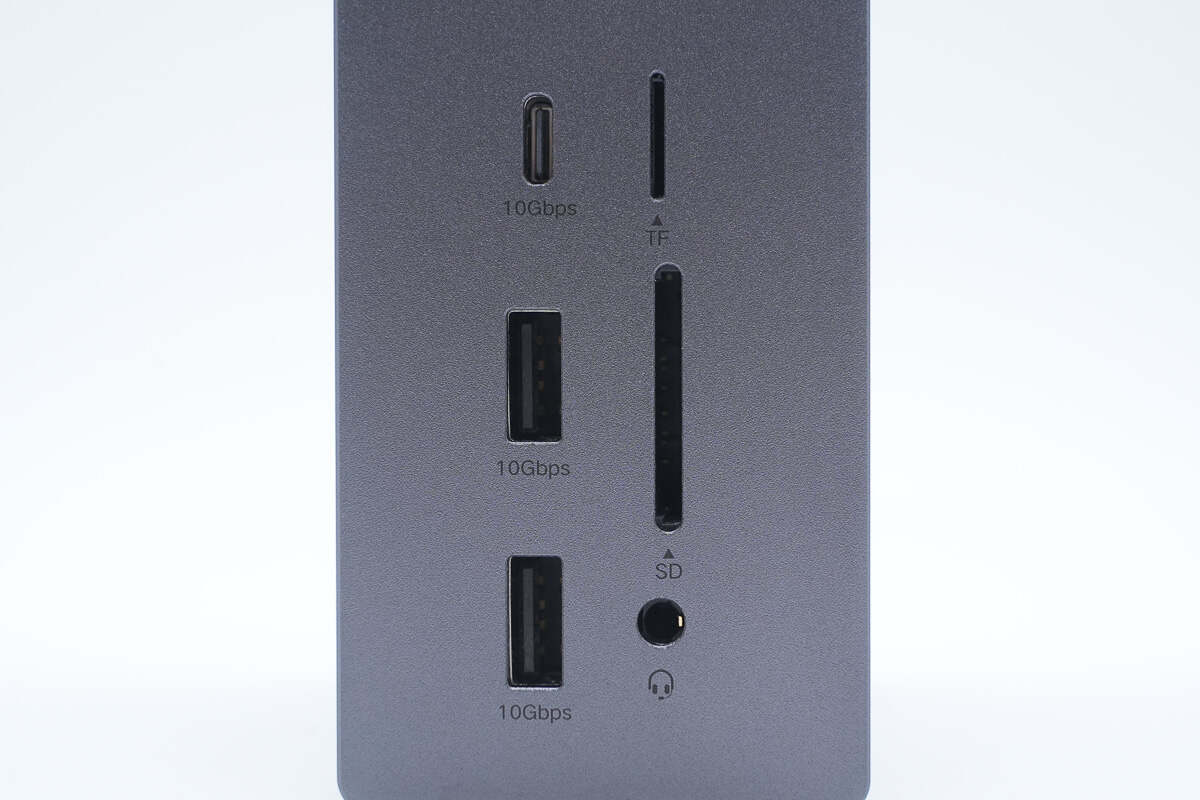
The ports are labeled with their respective data transfer rates.
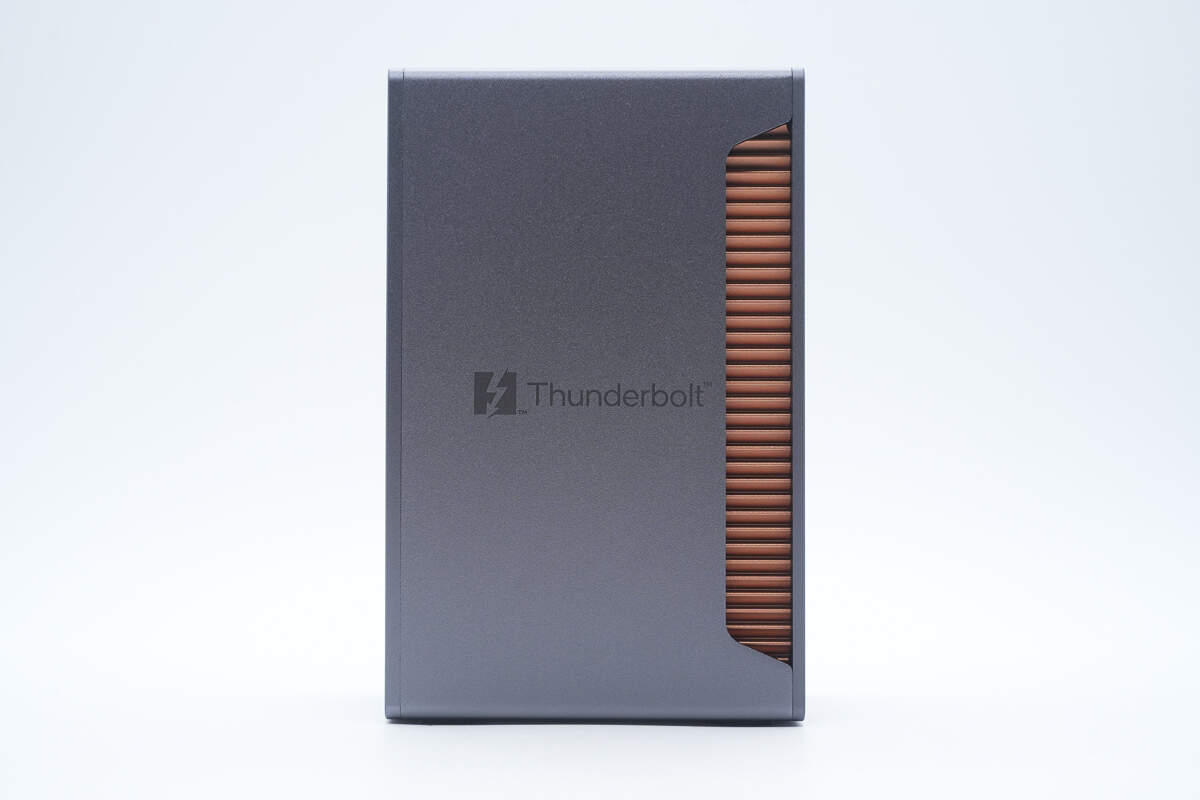
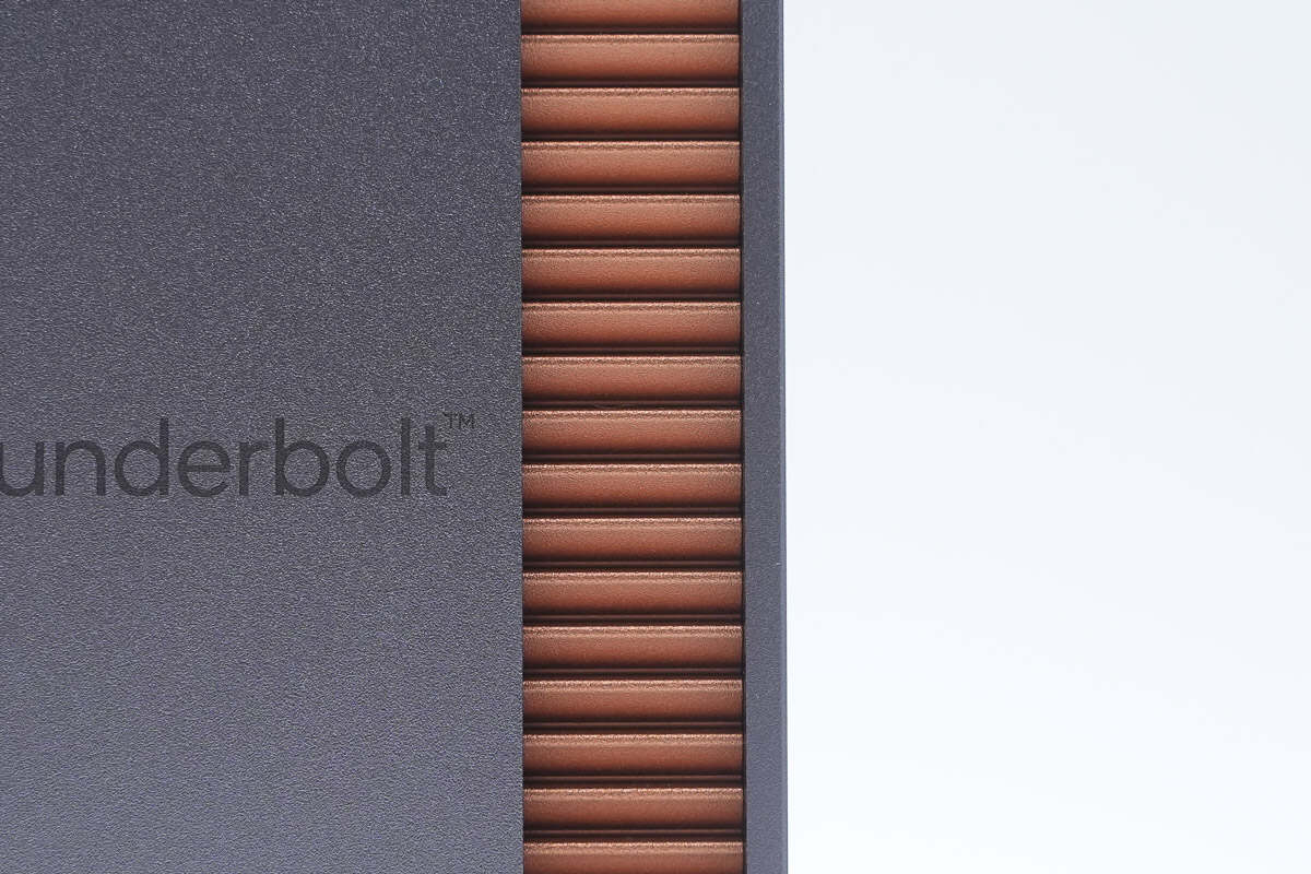
The side features the Thunderbolt logo.
Inside, there are heatsinks installed.
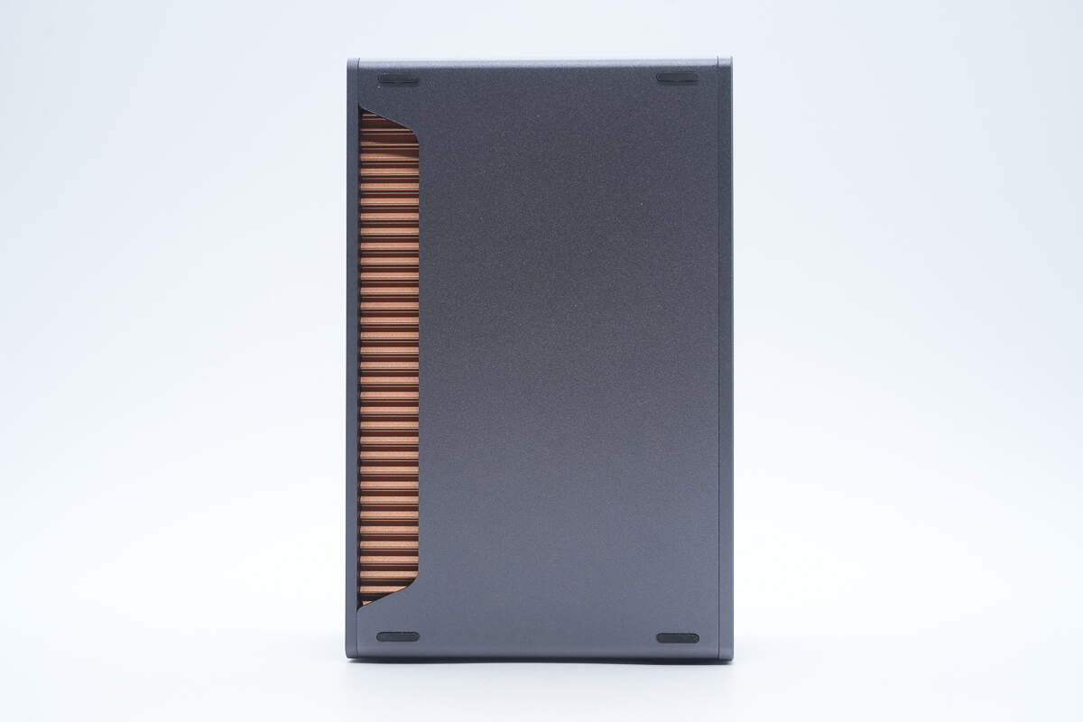
The other side also has heatsinks and is equipped with anti-slip pads.
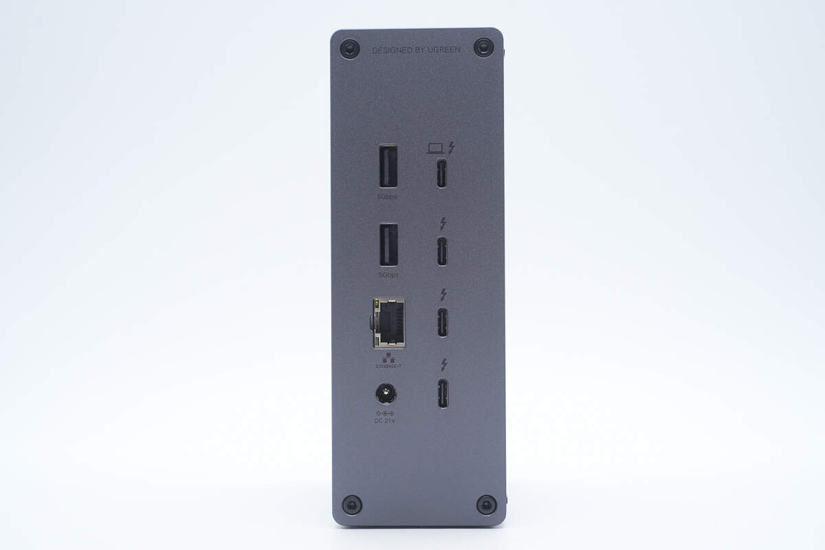
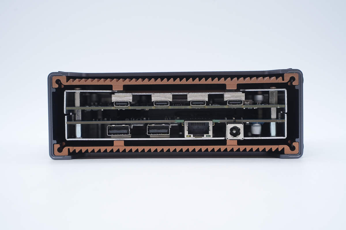
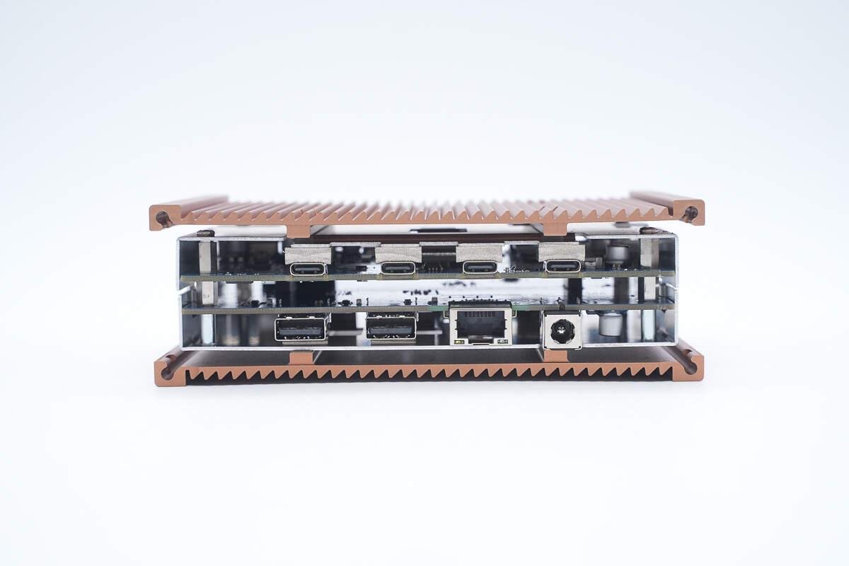
The back has Thunderbolt 5 ports, USB-A ports, an Ethernet port, and a power input slot.
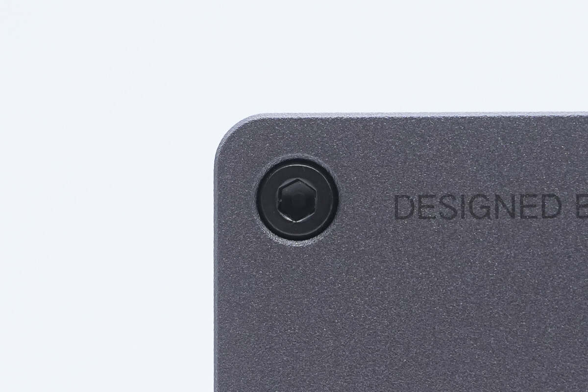
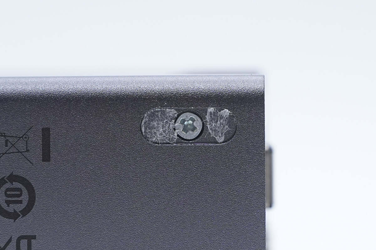
The back cover is secured with Allen screws.
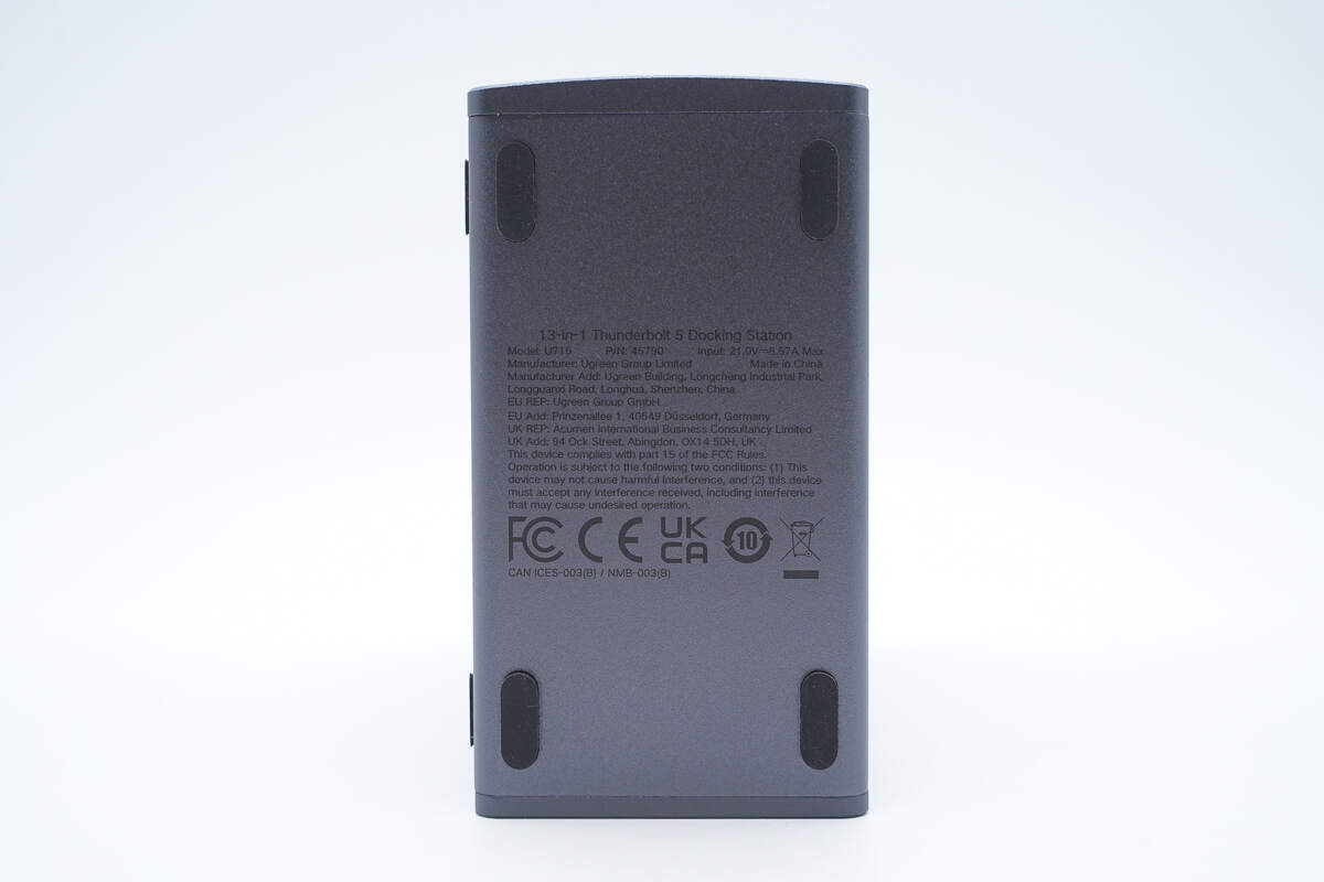
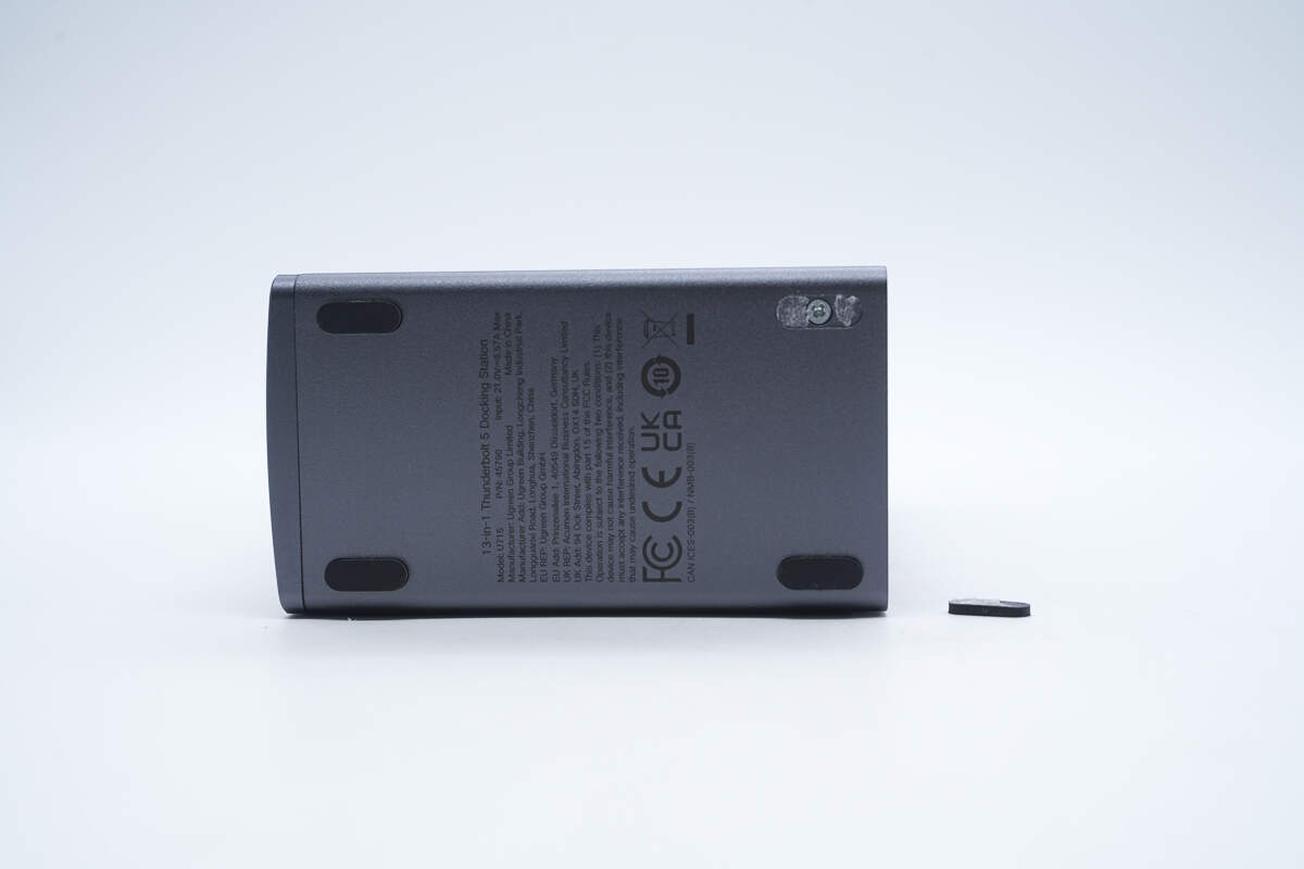
The bottom has anti-slip pads and printed product information.
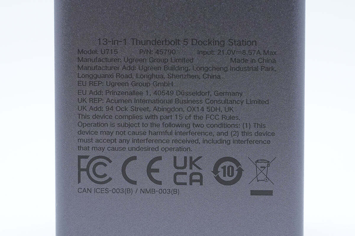
Model: U715
P/N: 45790
Input: 21V8.57A Max
It has passed FCC, CE, and UKCA certifications.
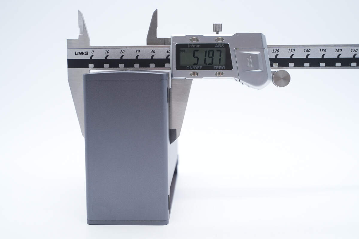
The width of the dock is about 52 mm (2.047 inches).
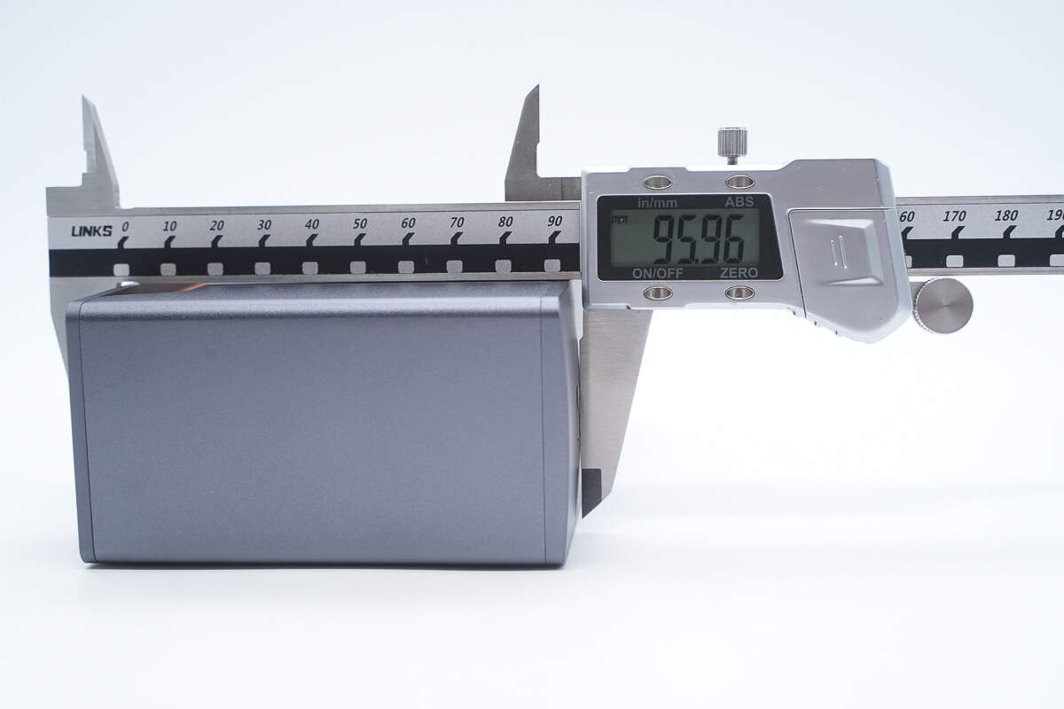
The thickness is about 96 mm (3.78 inches).
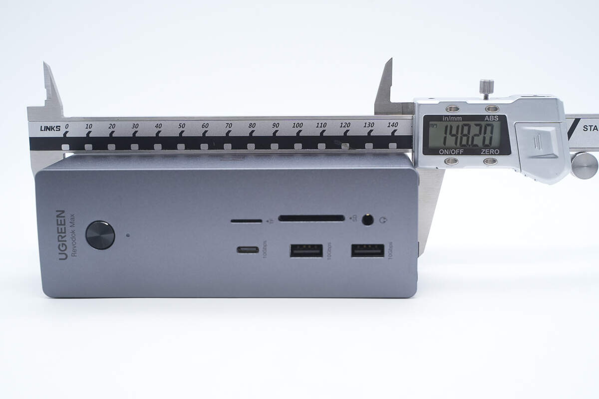
The height is about 148.2 mm (5.83 inches).
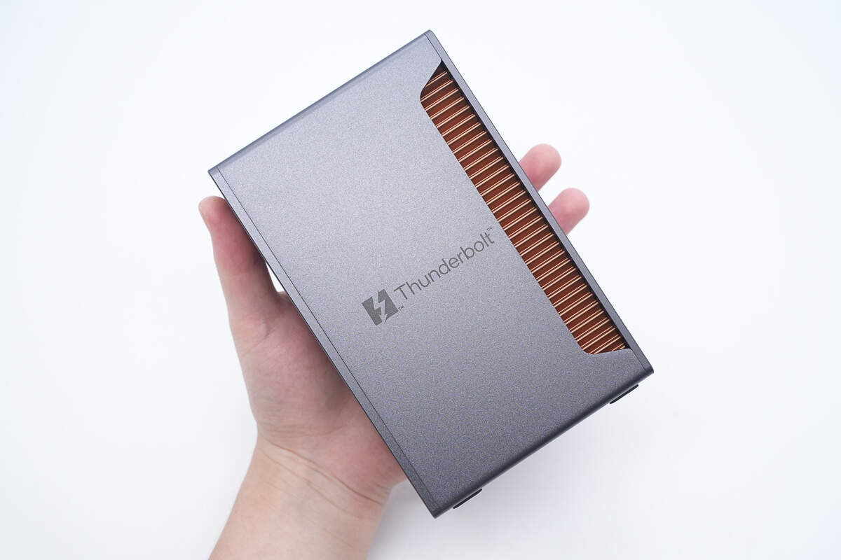
That's how big it is in the hand.
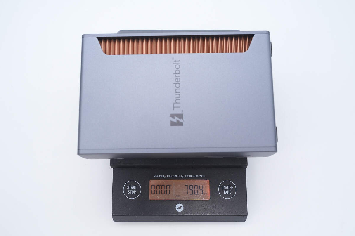
The weight is about 790 g (27.87 oz).
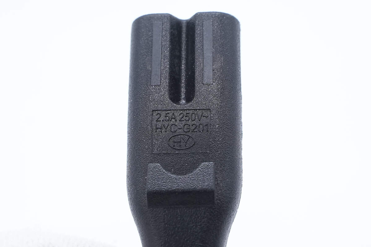
The included power cable has a C8 connector.
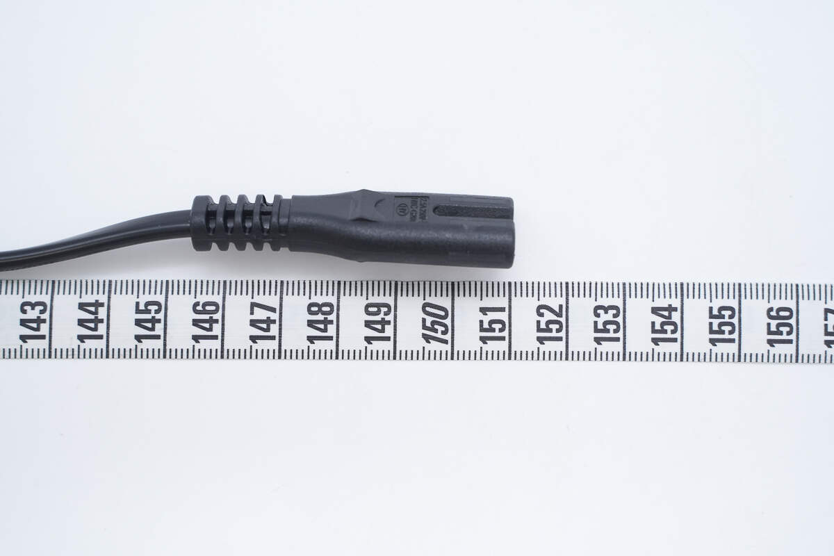
The length of the cable is about 151 cm (59.45 inches).
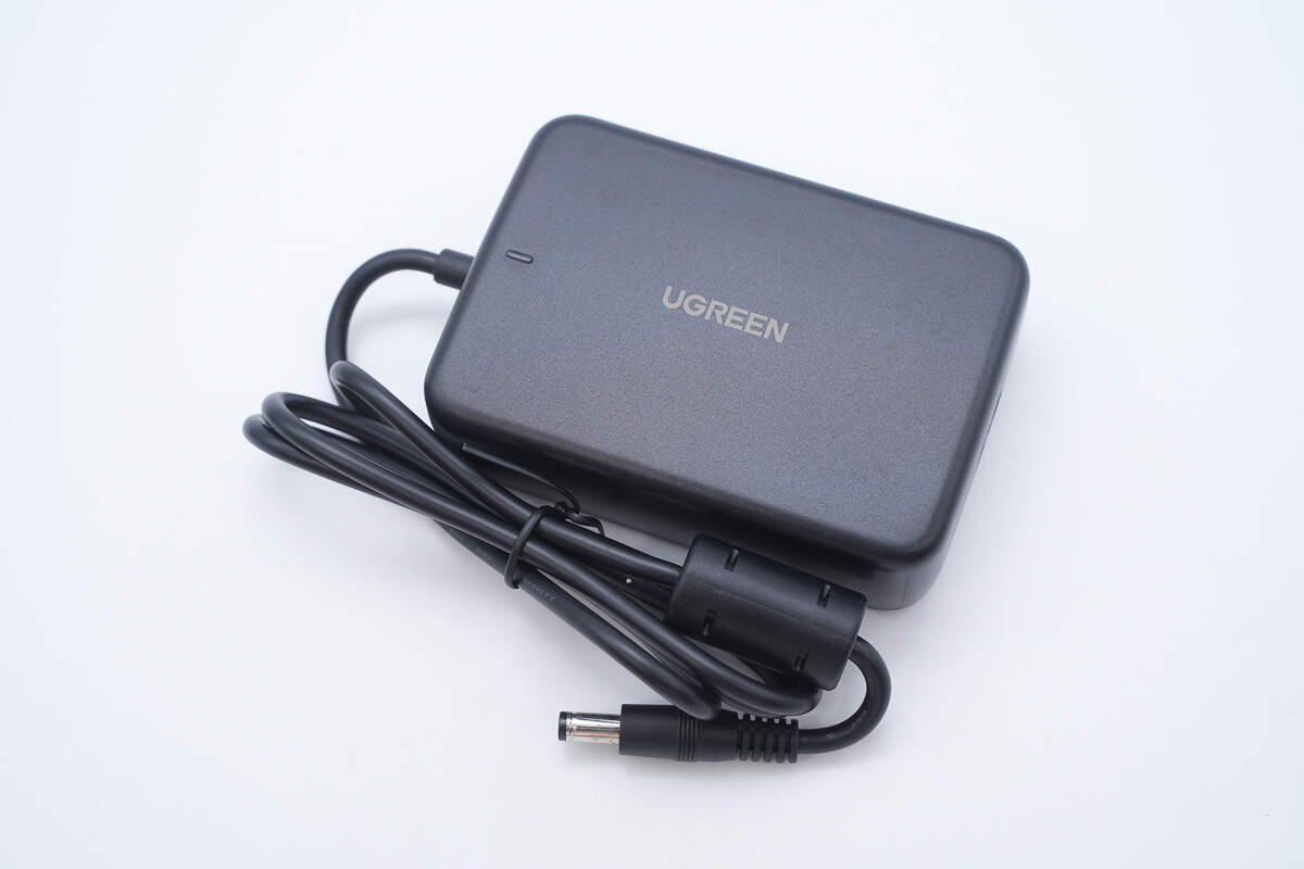
The included power adapter features an integrated cable design.
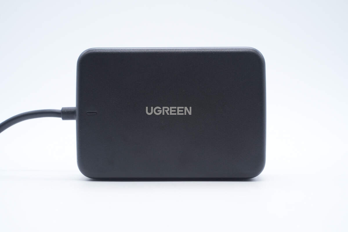
The front is printed with UGREEN and has an indicator light.
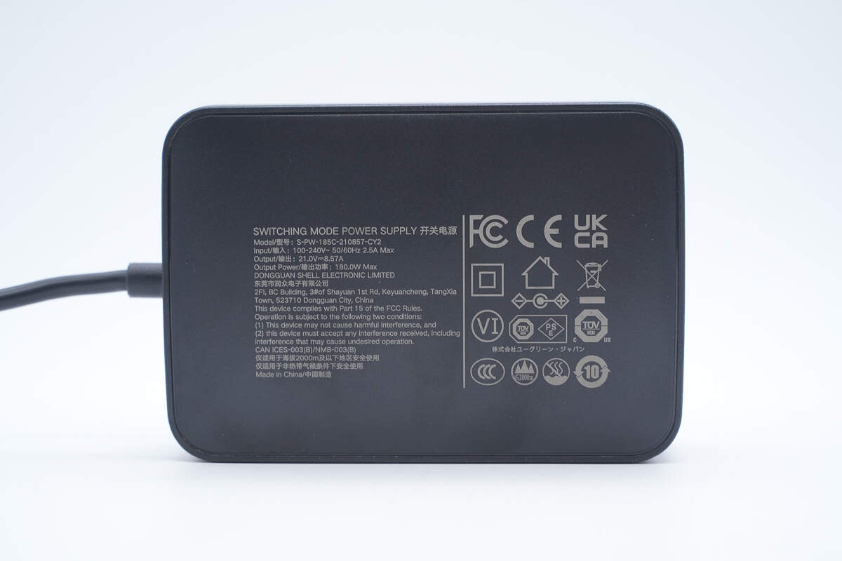
The spec info is printed on the back.
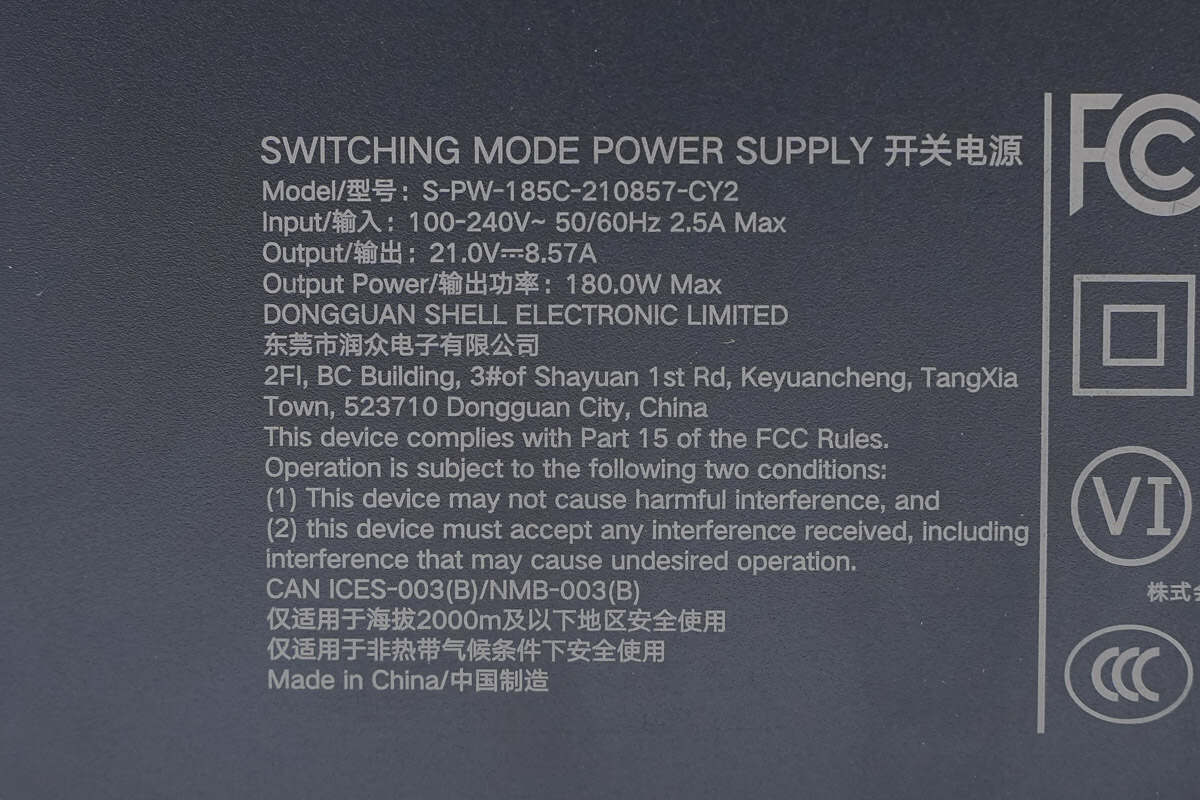
Model: S-PW-185C-210857-CY2
Input: 100-240V~ 50/60Hz 2.5A Max
Output: 21V 8.57A
Output Power: 180W Max
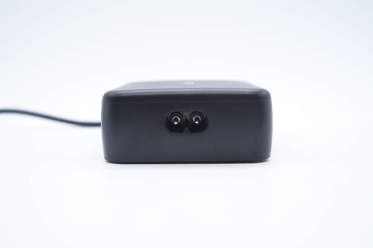
The power input features a C8 socket.
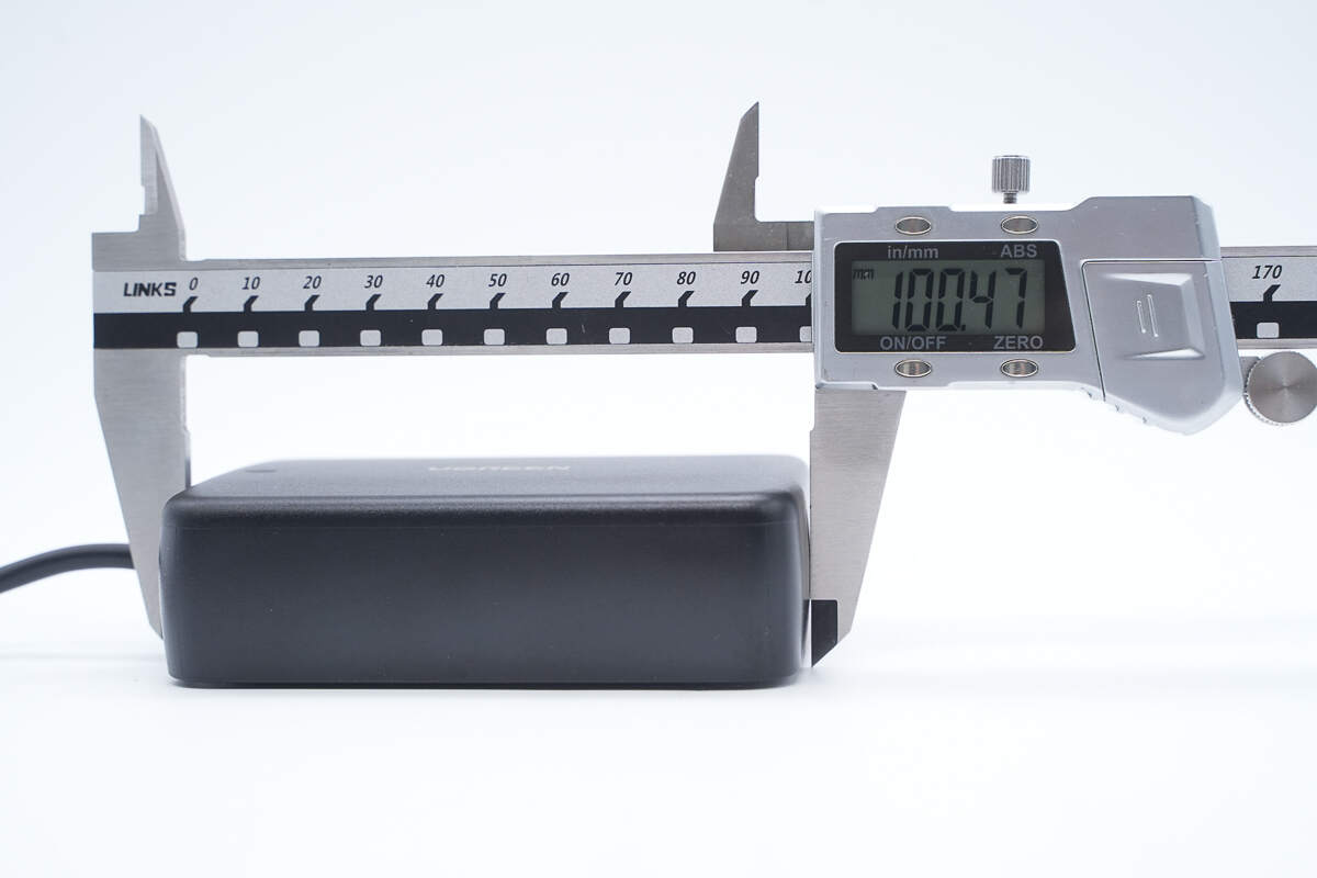
The length is about 100.5 mm (3.96 inches).
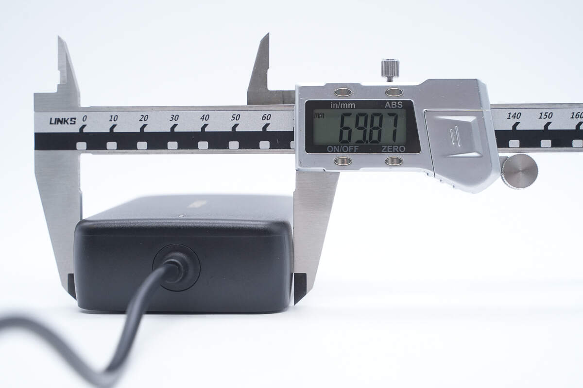
The width is about 69.9 mm (2.75 inches).
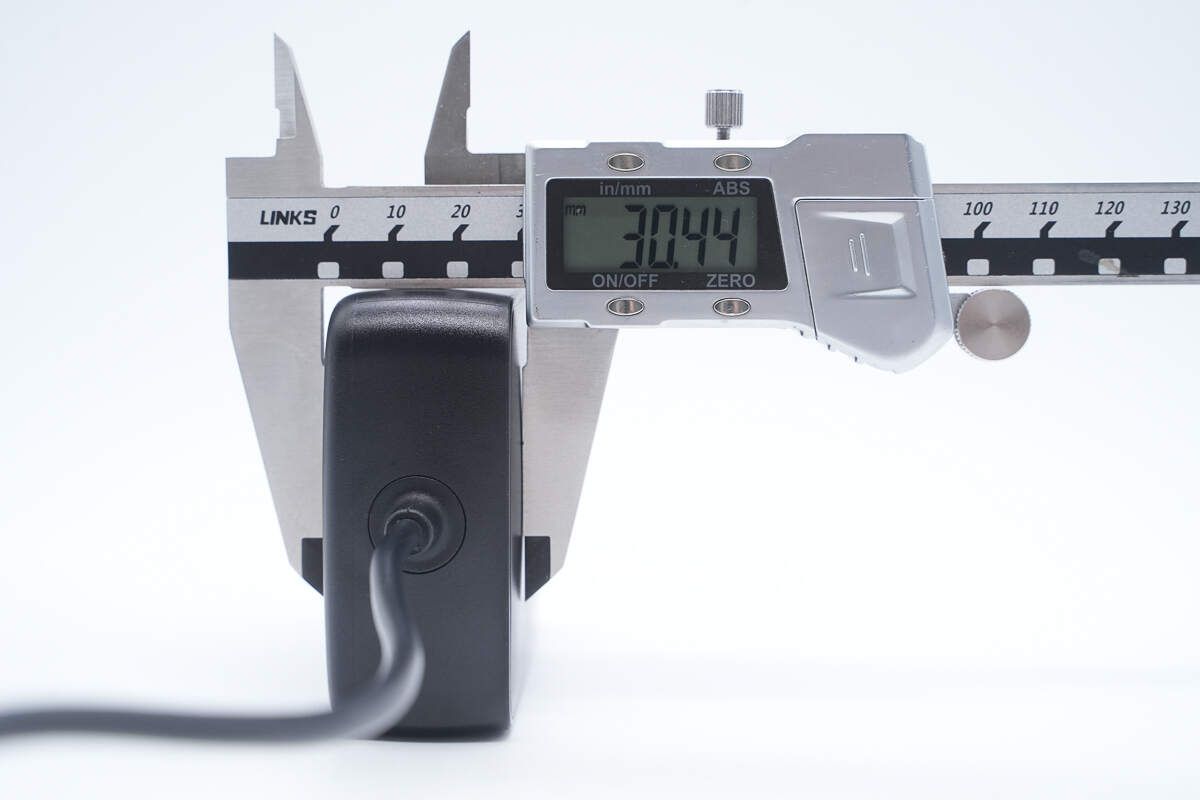
The thickness is about 30.4 mm (1.2 inches).
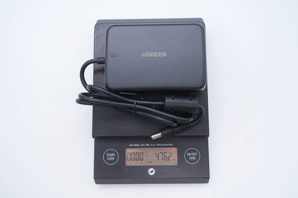
The weight is about 476 g (16.79 oz).
The output is a DC connector.
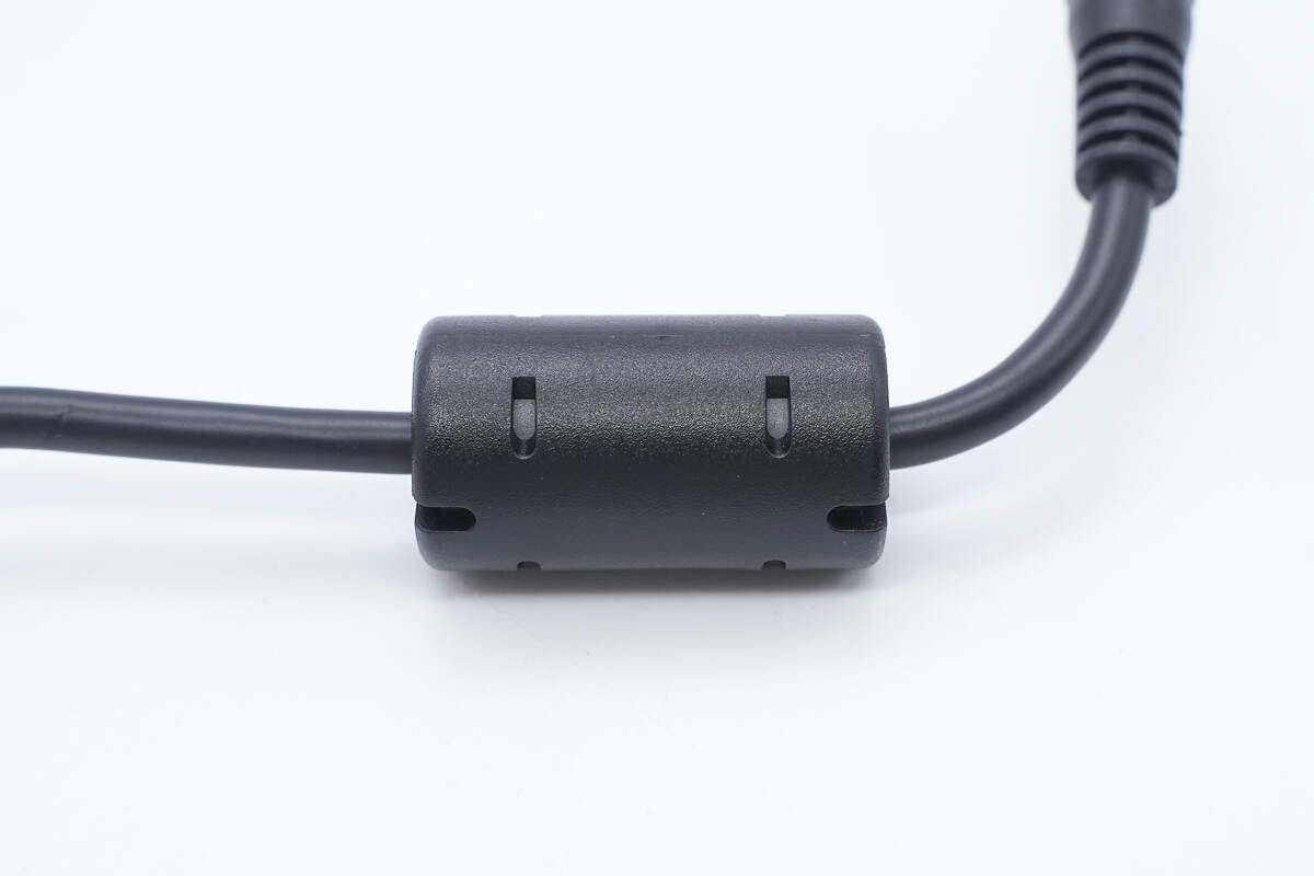
The output cable is equipped with an anti-interference ferrite core.
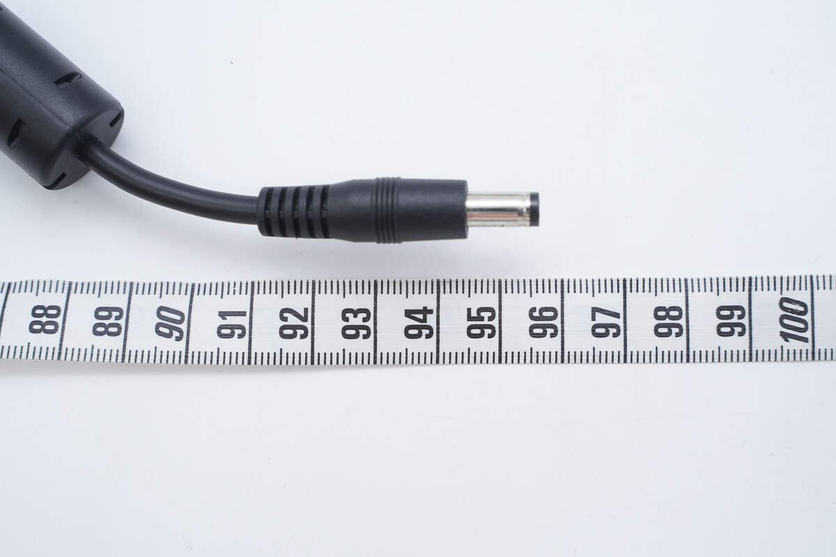
The length of the output cable is about 96 cm (37.8 inches).
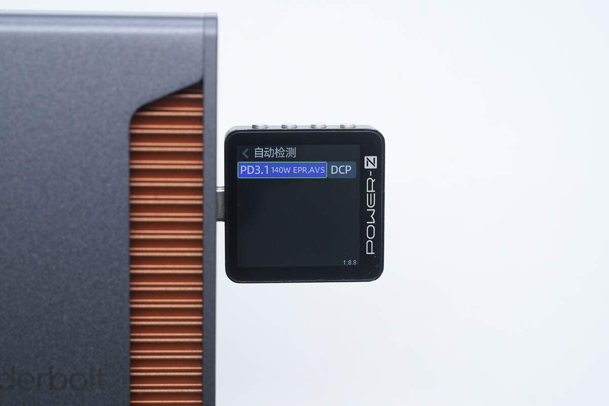
ChargerLAB POWER-Z KM003C measured that the Thunderbolt 5 upstream port supports PD3.1 140W charging protocol and DCP charging protocol.
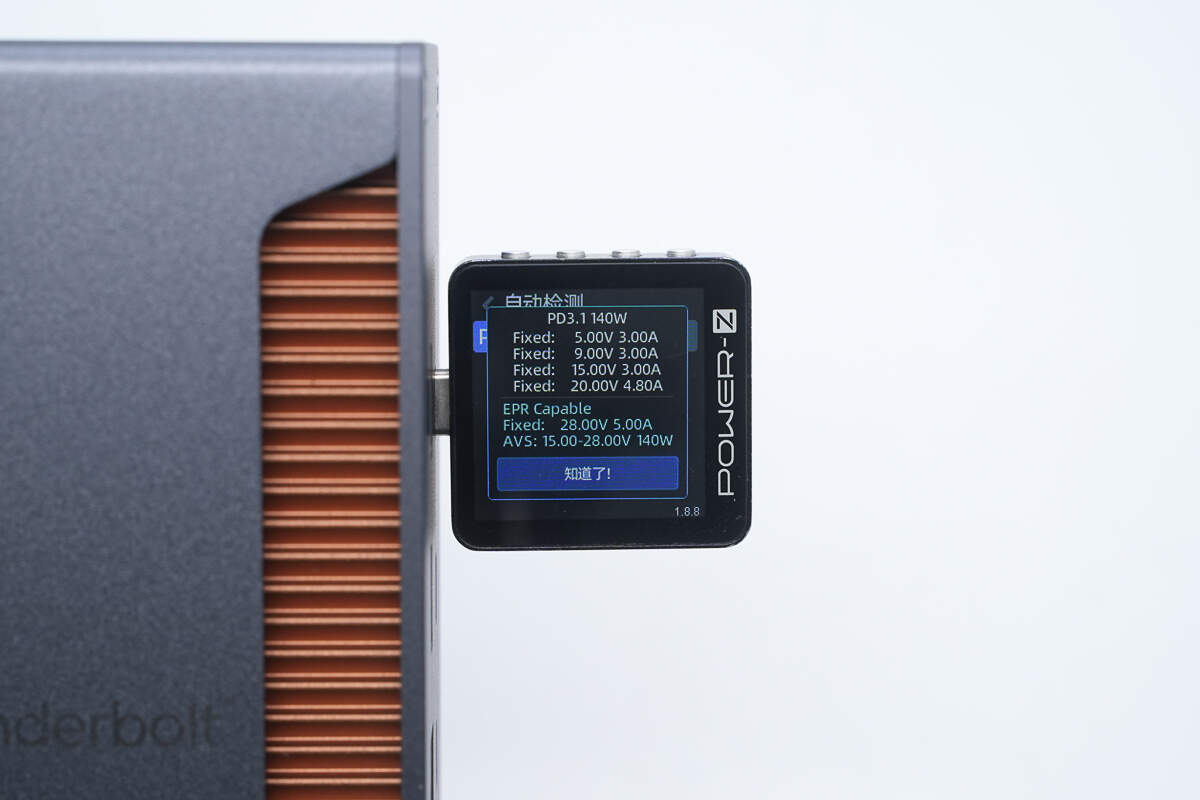
And it has five fixed PDOs of 5V3A, 9V3A, 15V3A, 20V4.8A, and 28V5A. It has one set of AVS, which is 15-28V 140W.
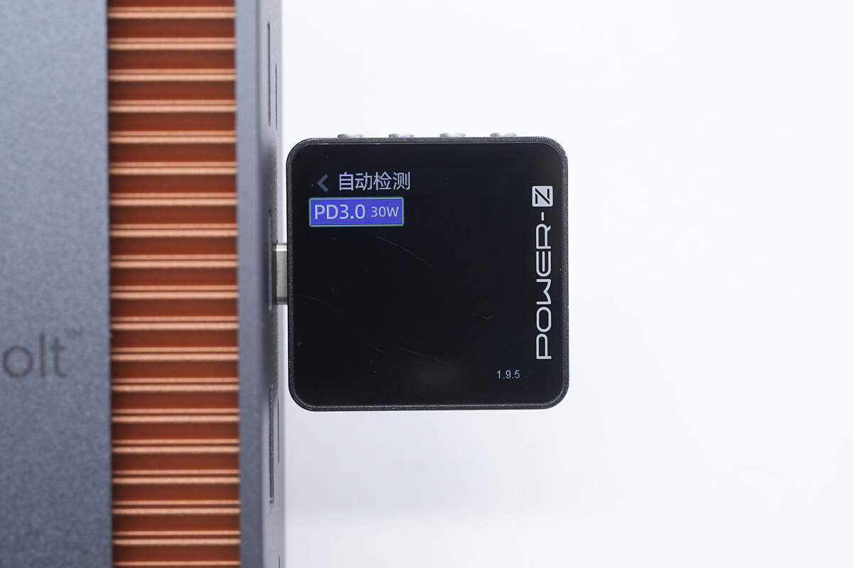
It was measured that Thunderbolt 5 downstream port A supports PD3.0 30W output.
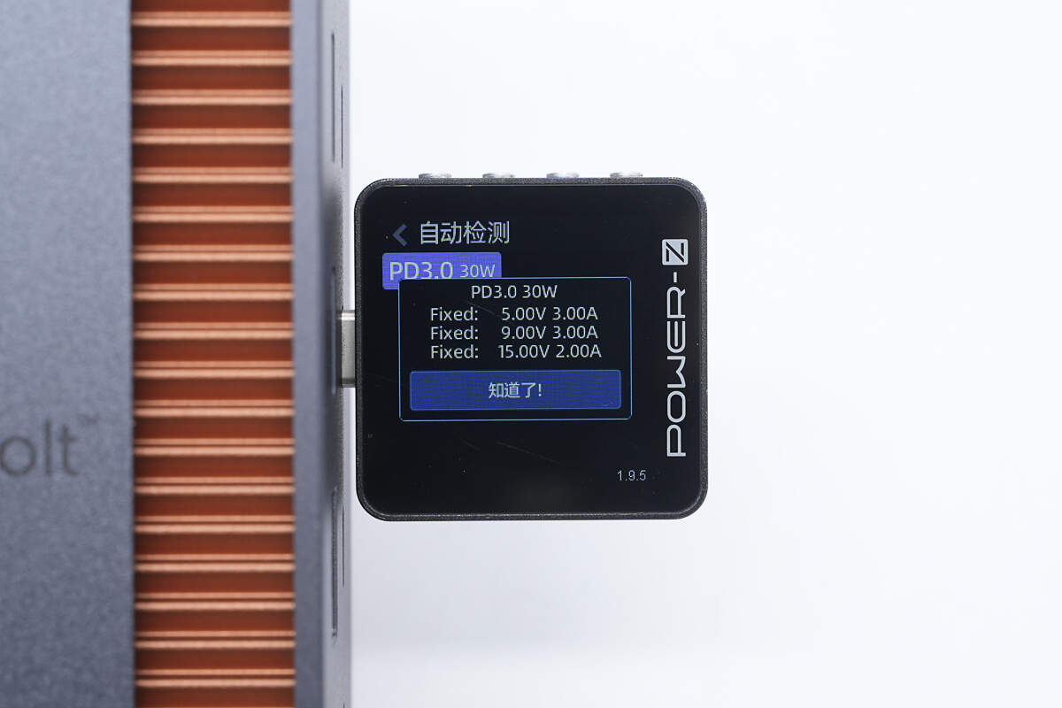
And it has three fixed PDOs of 5V3A, 9V3A, and 15V2A.
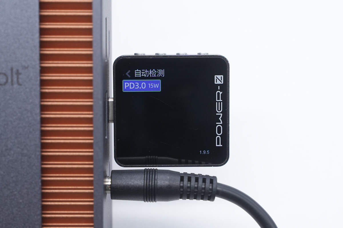
Thunderbolt 5 downstream ports B and C support PD3.0 15W output.
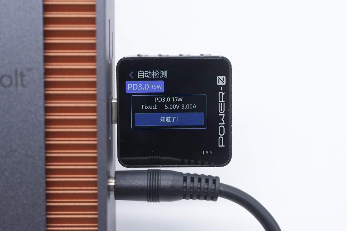
And it has one fixed PDO of 5V3A.
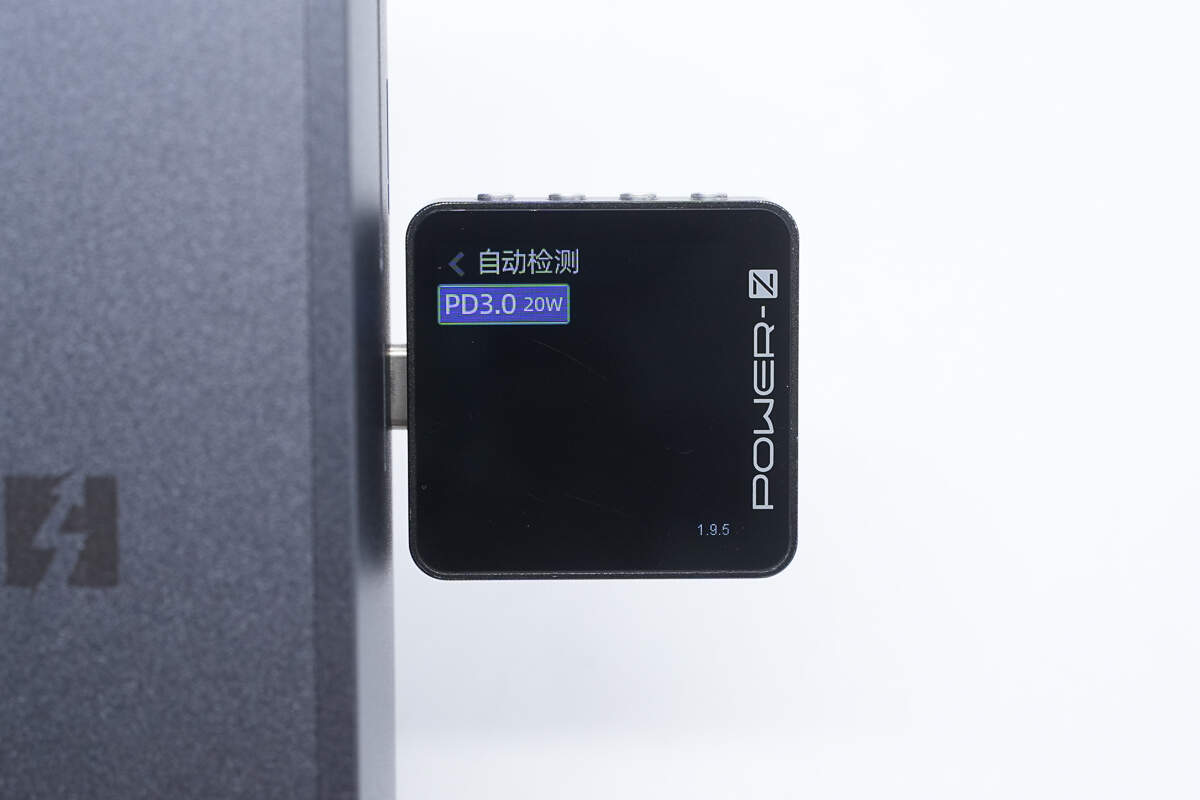
The front USB-C port supports 20W PD.
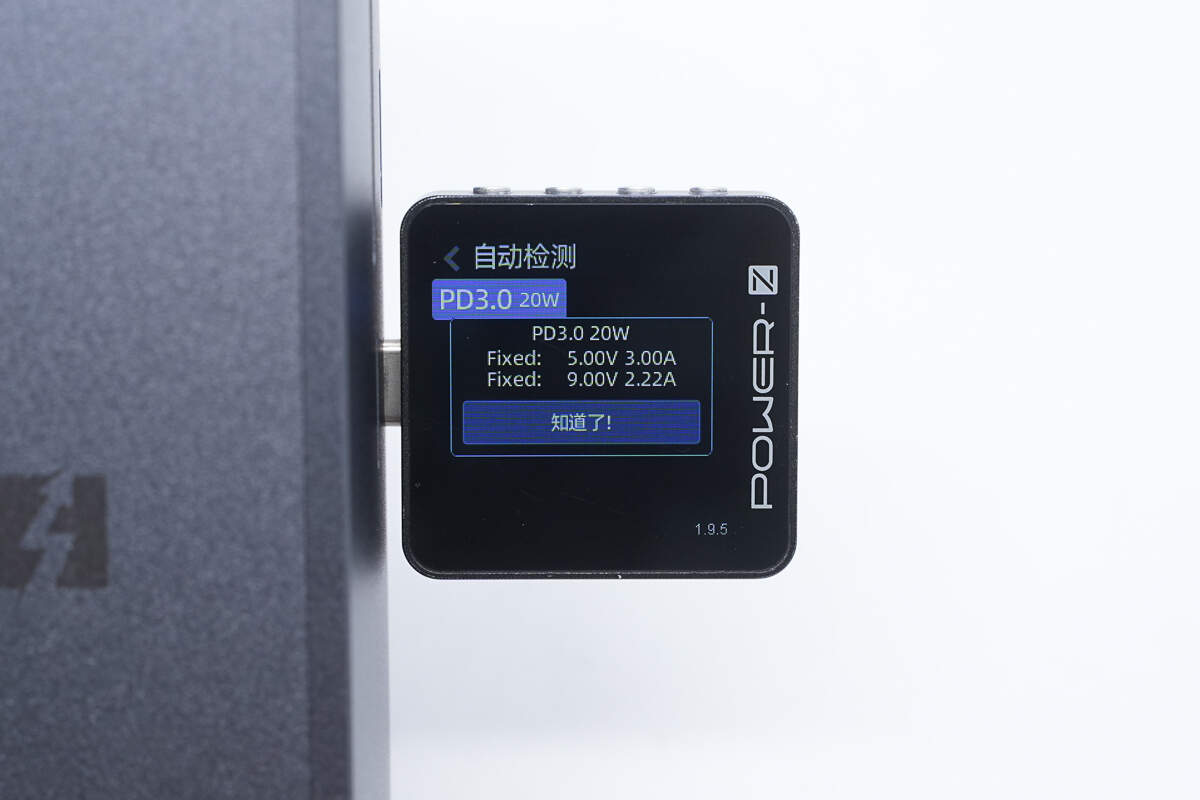
And it has two fixed PDOs of 5V3A and 9V2.22A.
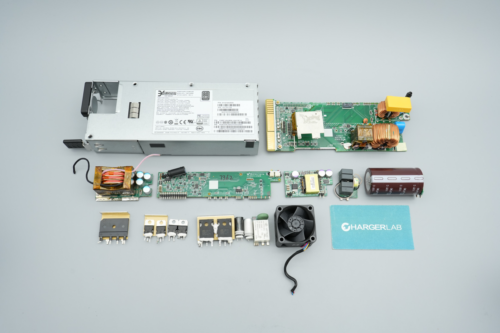
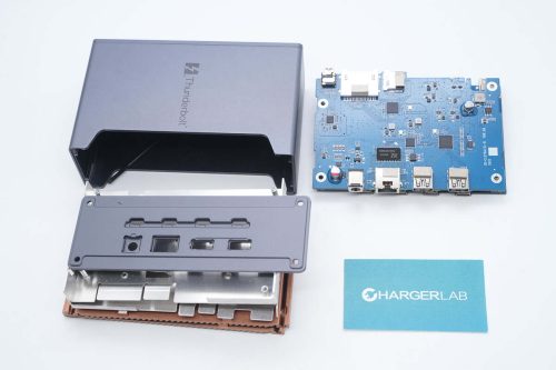
Teardown
Next, let's take it apart to see its internal components and structure.
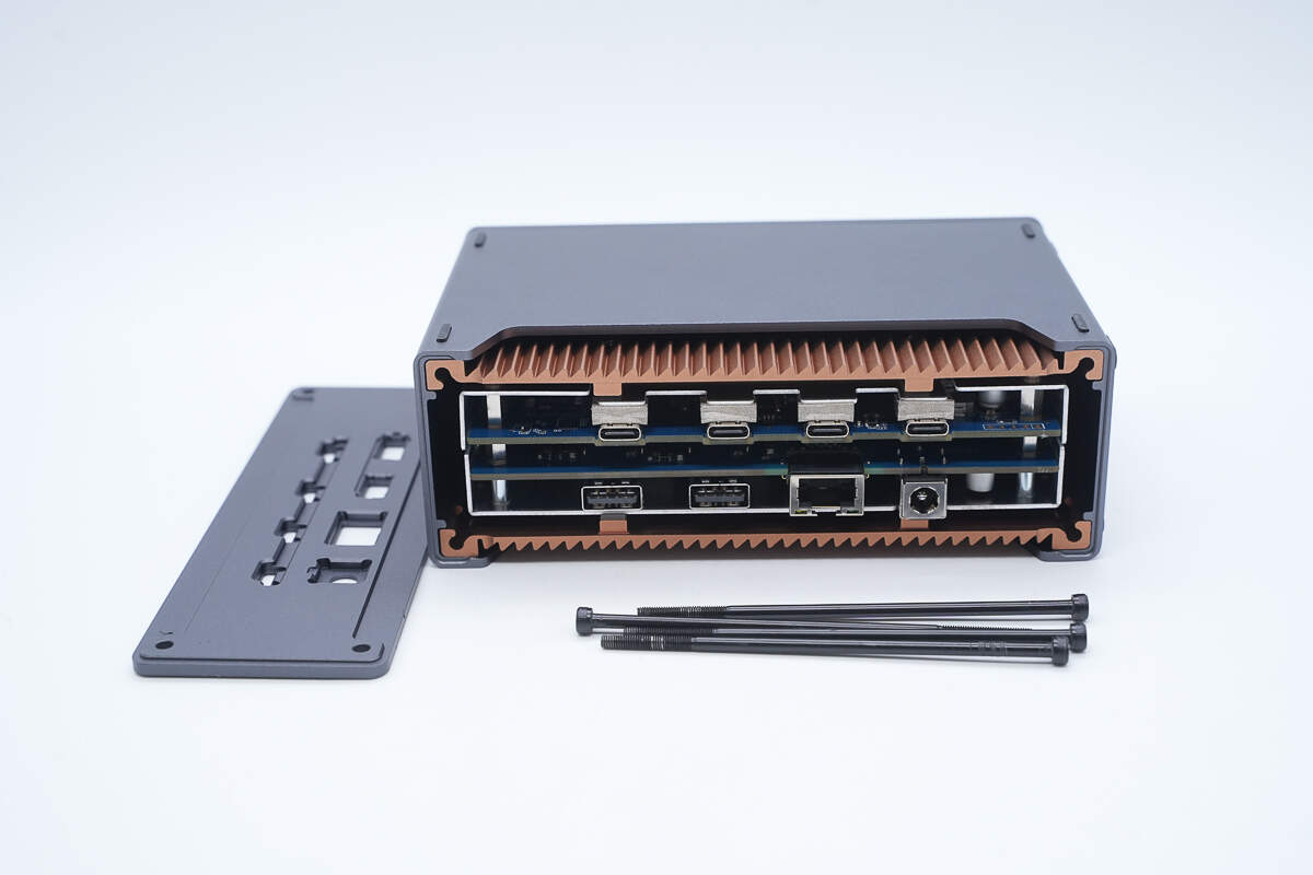
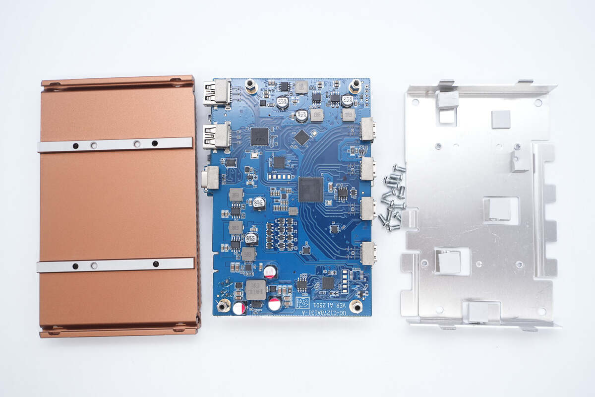
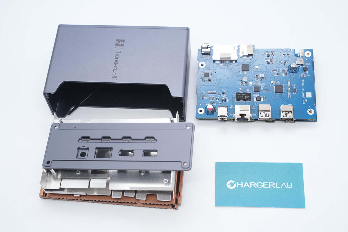
First, unscrew the four long screws to remove the back cover.
The PCBA module is equipped with aluminum alloy shielding covers, and conductive fabric is applied between the ports and the casing for grounding.
Peel off the anti-slip pads from the bottom.
There are screws underneath the pads.
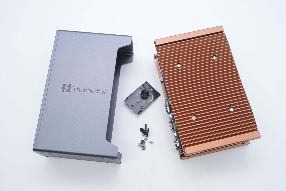
Unscrew the screws and remove the PCBA module.
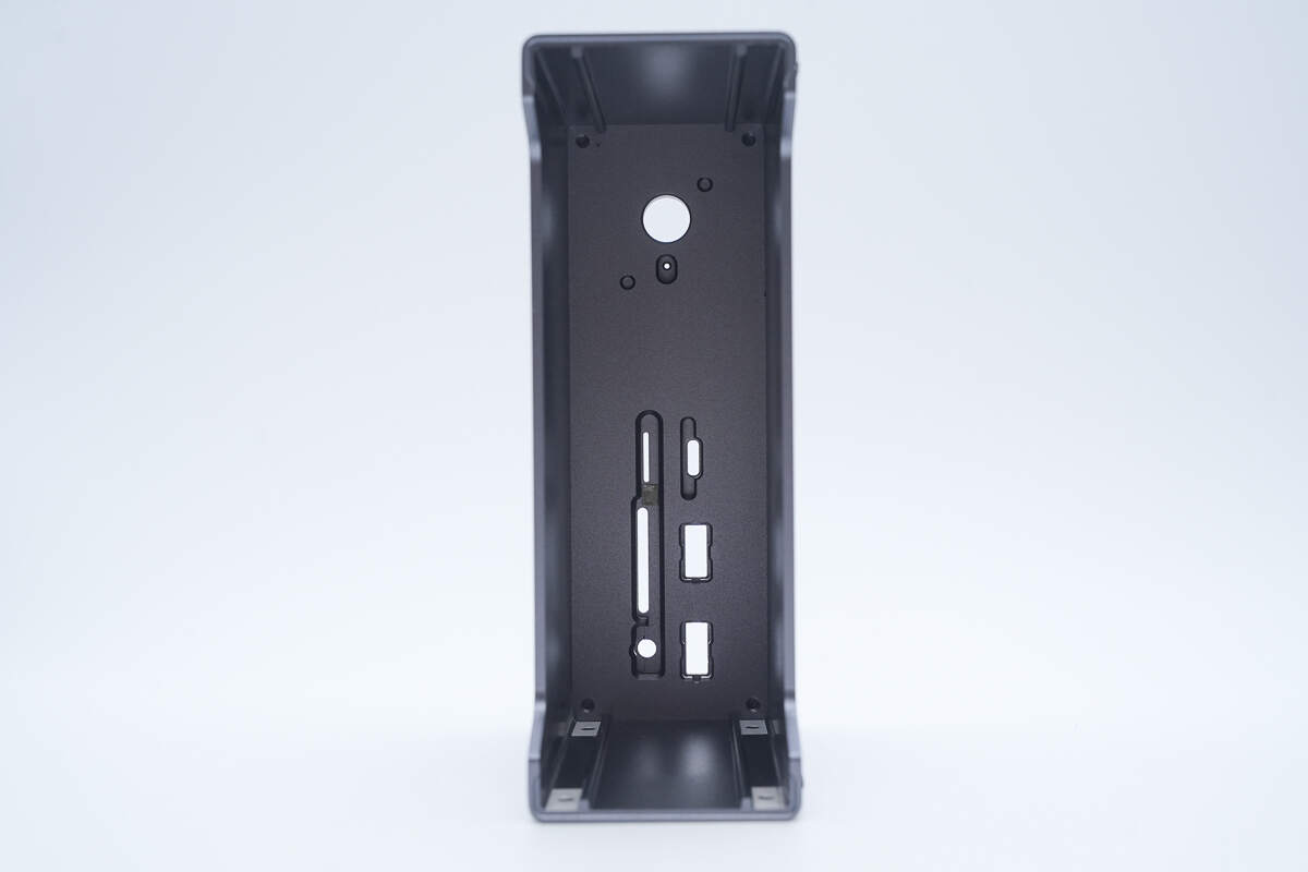
The casing is made of aluminum alloy.
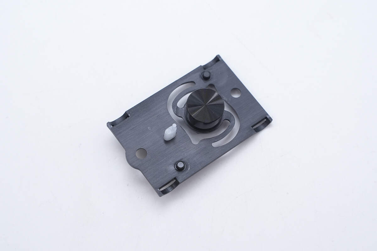
Close-up of the power button and the light guide for the indicator LED.
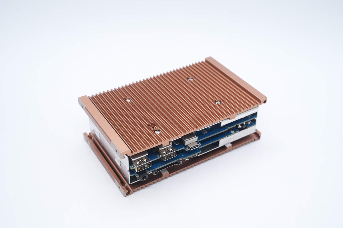
The PCBA module has aluminum alloy heatsinks on both sides.
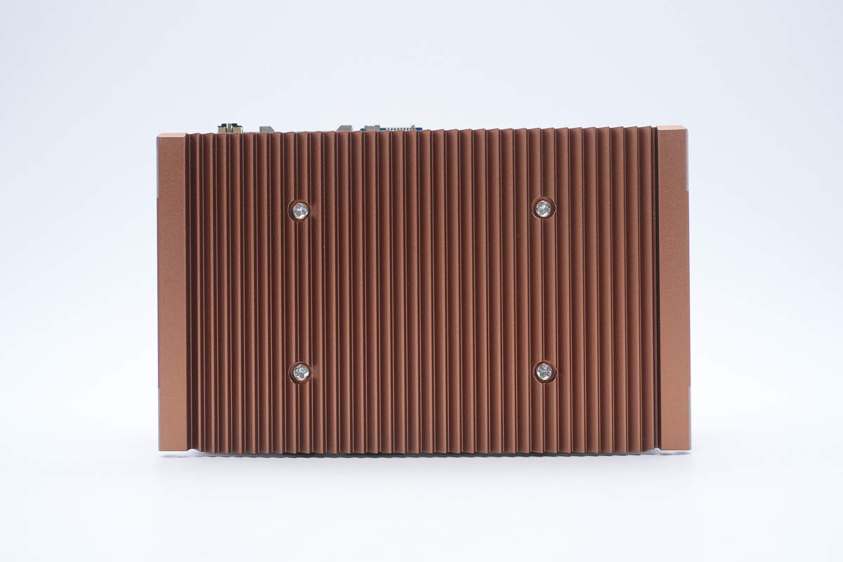
The heatsinks are secured with screws.
The heatsinks are attached to the shielding cover.
After removing the heatsinks and shielding cover, thermal pads are placed on the shielding cover corresponding to the heat-generating components.
The PCBA module is secured with standoffs.
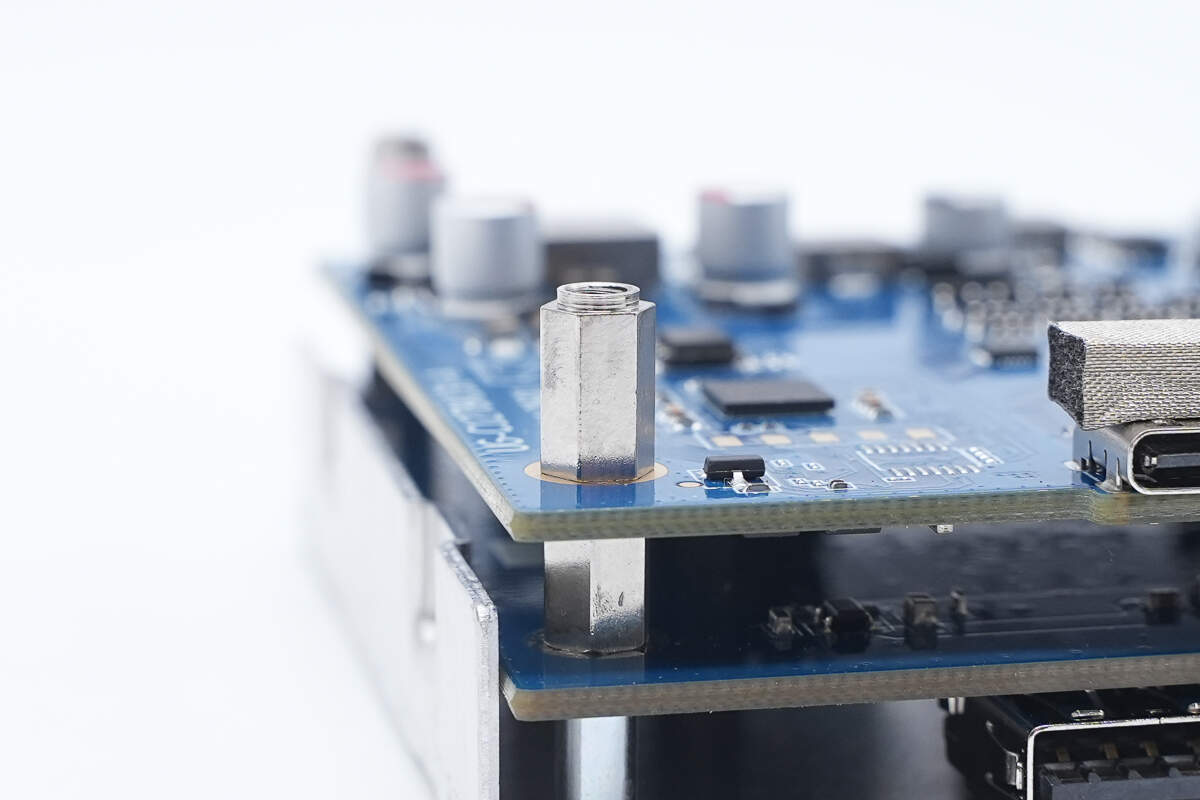
Close-up of the standoffs securing the PCBA module.
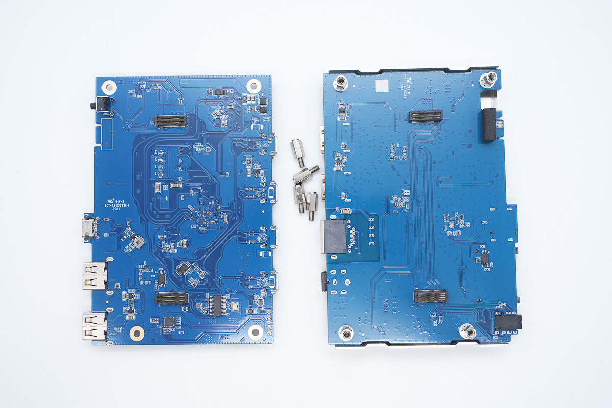
Separate the two PCBs.
There are also thermal pads between the other side of the PCB and the shielding cover.
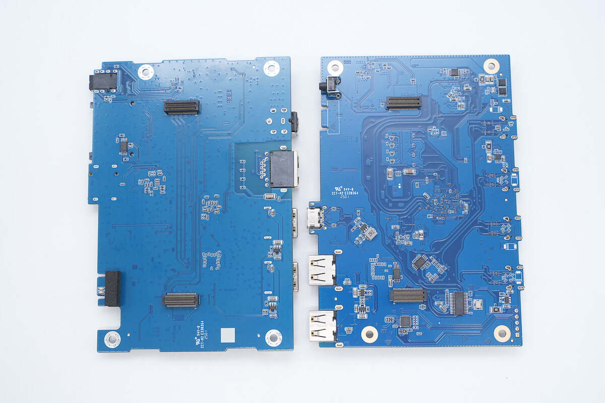
The two PCBs are connected through connectors.
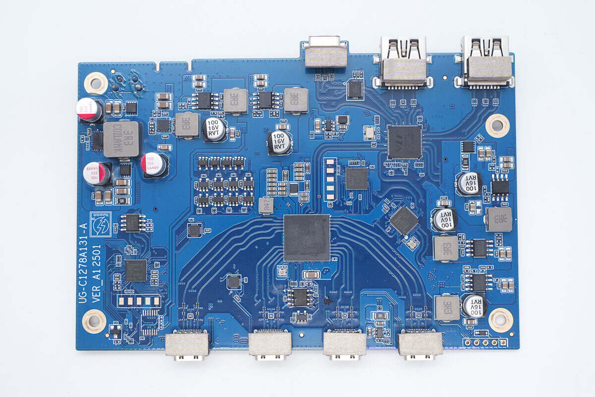
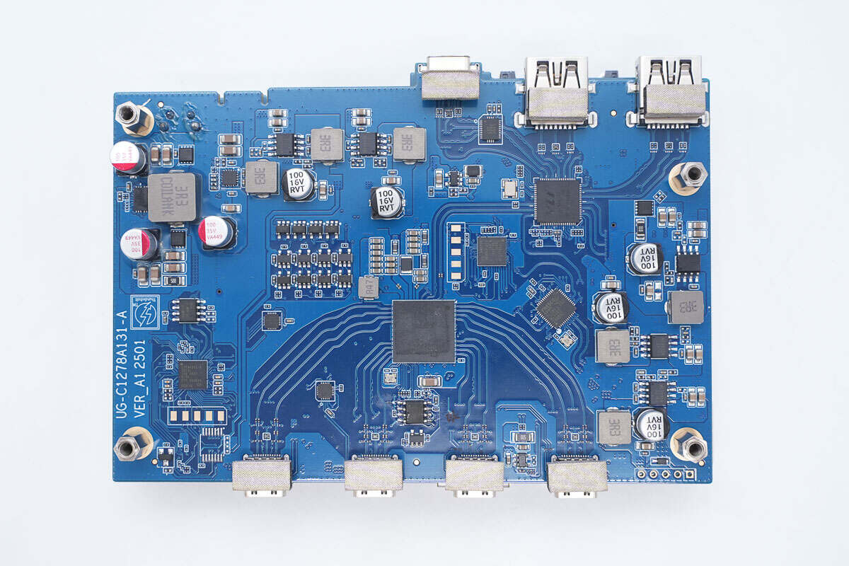
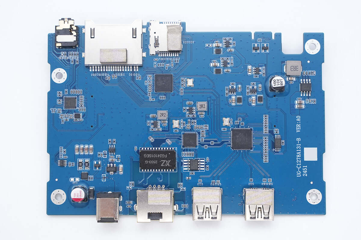
On the bottom side of the Thunderbolt 5 interface PCB, there are four Thunderbolt 5 ports and the Thunderbolt controller. The upper left area contains synchronous buck-boost and synchronous buck circuits. The lower left area houses protocol chips. The upper right corner has USB ports and a hub chip. The right side includes synchronous buck circuits, a hub chip, and protocol chips.
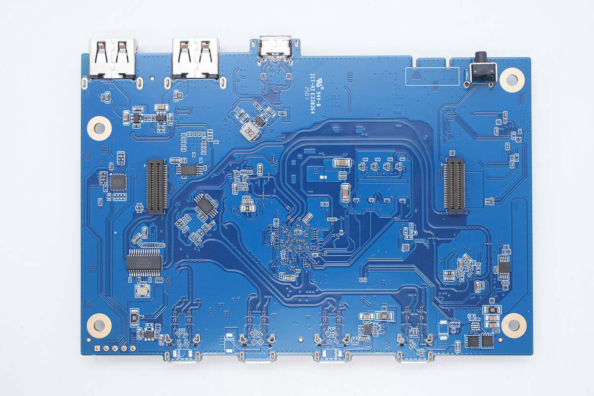
The back side has connectors, protocol chips, hub chips, memory, and VBUS MOSFETs. It also features synchronous buck chips and overcurrent protection chips.
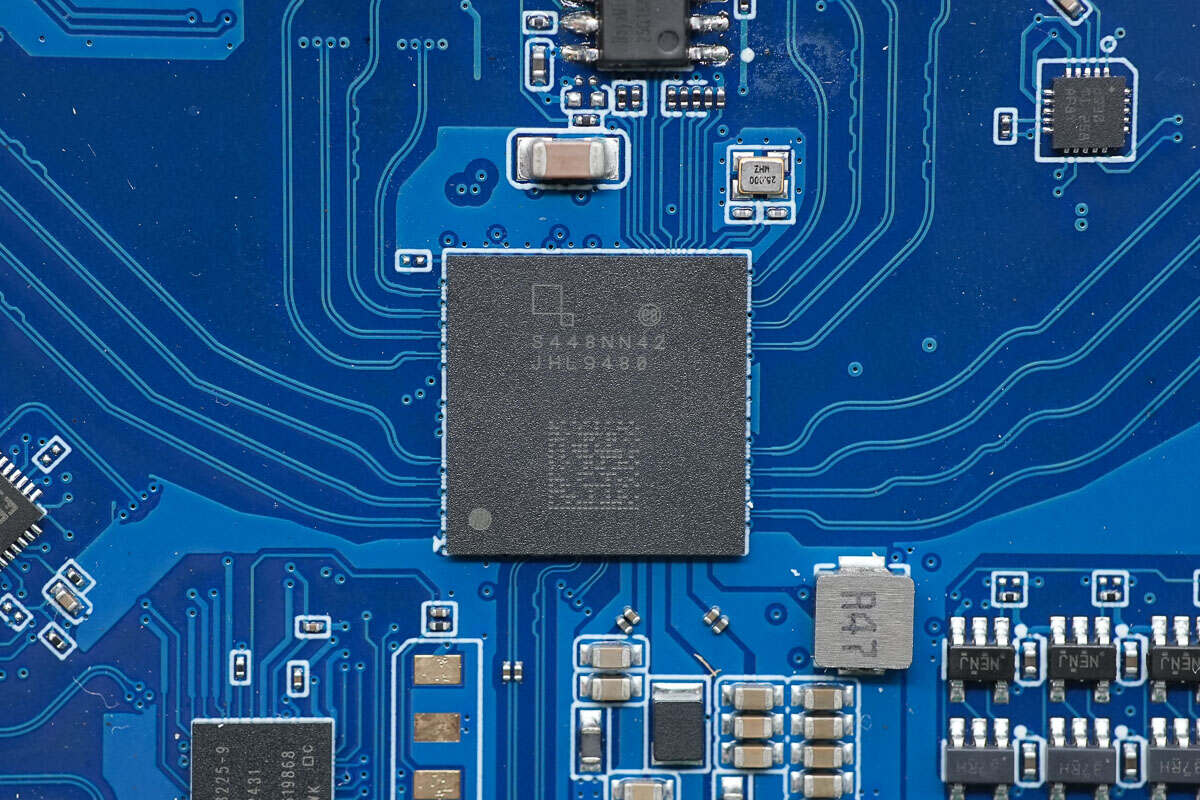
The Thunderbolt controller is from Intel, model JHL9480, codenamed Barlow Ridge. It supports four PCIe lanes configured as x4 Gen 4 and includes features such as ACS, FBP, PTM, and P2P. It supports 128/256B payloads. For display ports, it provides 2 DP sinks and 3 DP sources, supports DP 2.1 tunneling and retiming functions, and operates in x1/x2/x4 modes with speeds ranging from 1.62Gbps to 20Gbps. It features SST, MST, DSC 1.2, FEC, LTTPR, Panel Replay, and uses an FC-CSP package.
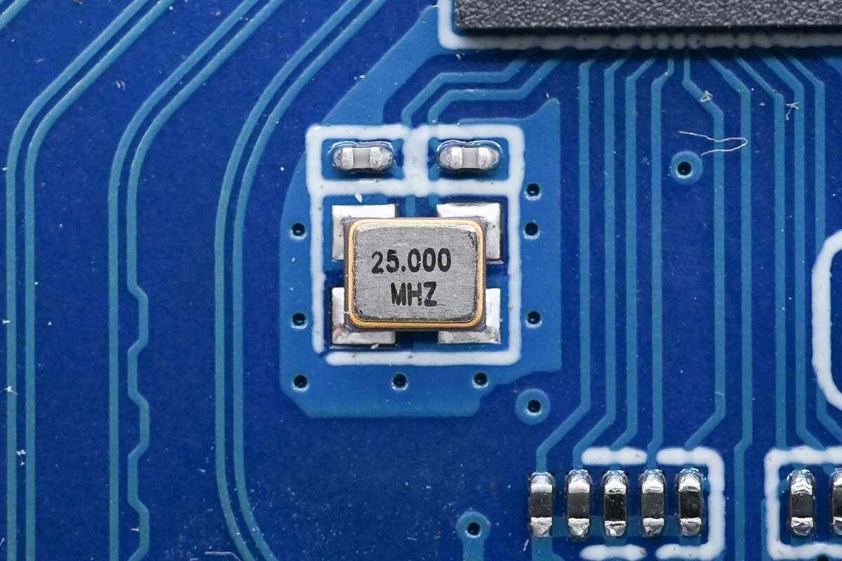
Close-up of the external 25.000 MHz clock crystal oscillator.
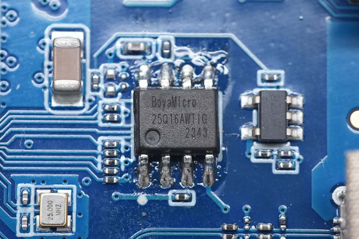
The memory is from BoyaMicro, model BY25Q16AWTIG, with a capacity of 2MB and packaged in SOP8.
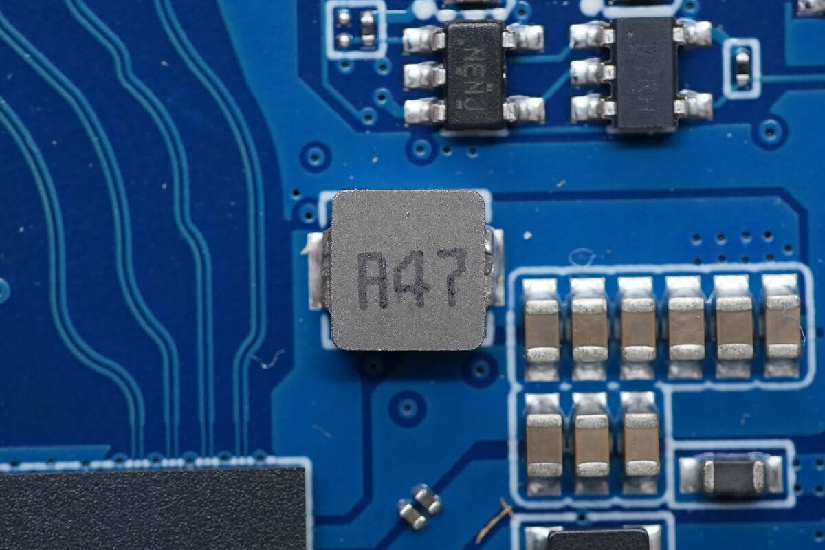
Close-up of the external 0.47μH buck inductor for the Thunderbolt controller.
Close-up of the external buck inductors.
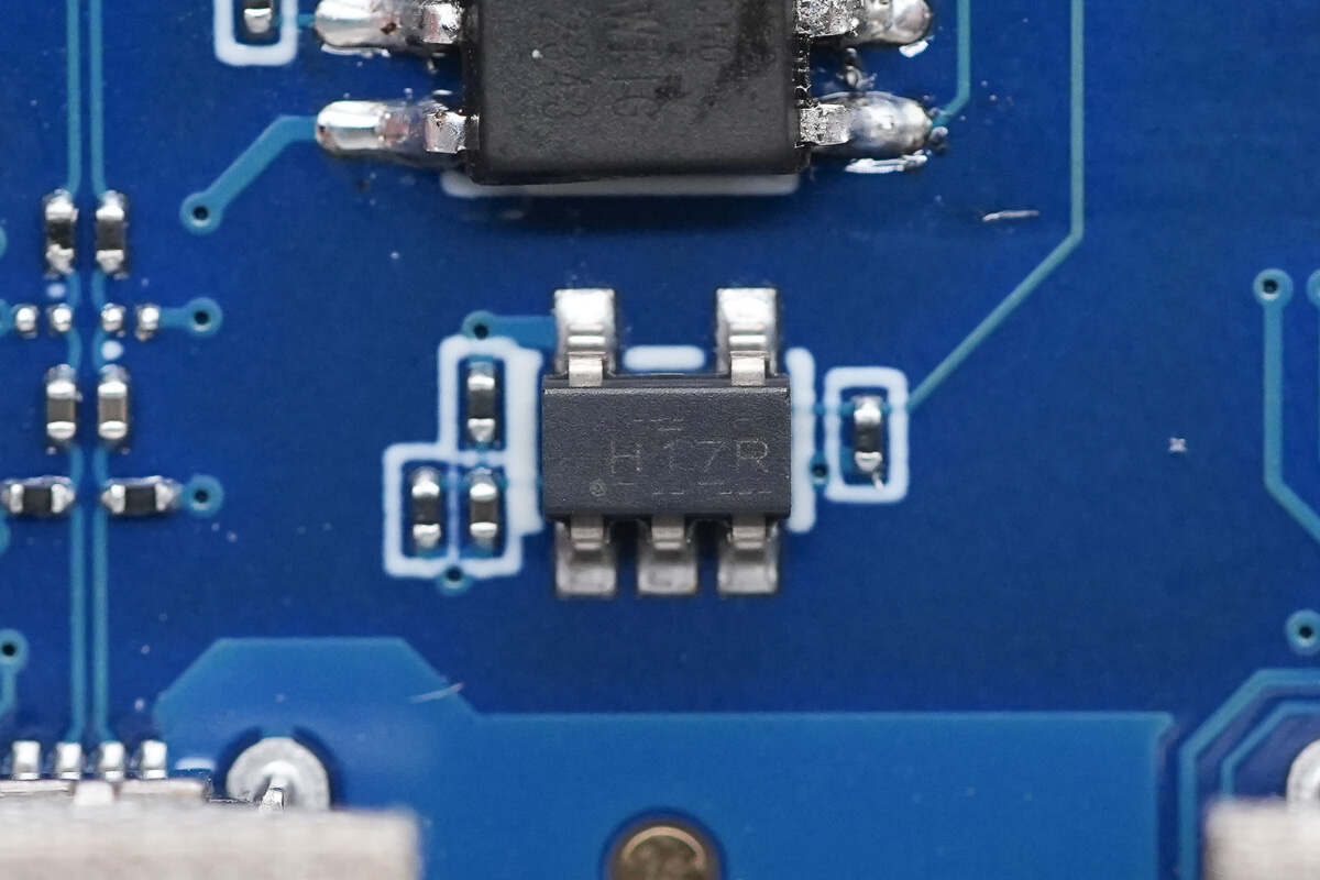
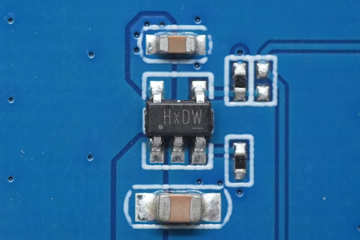
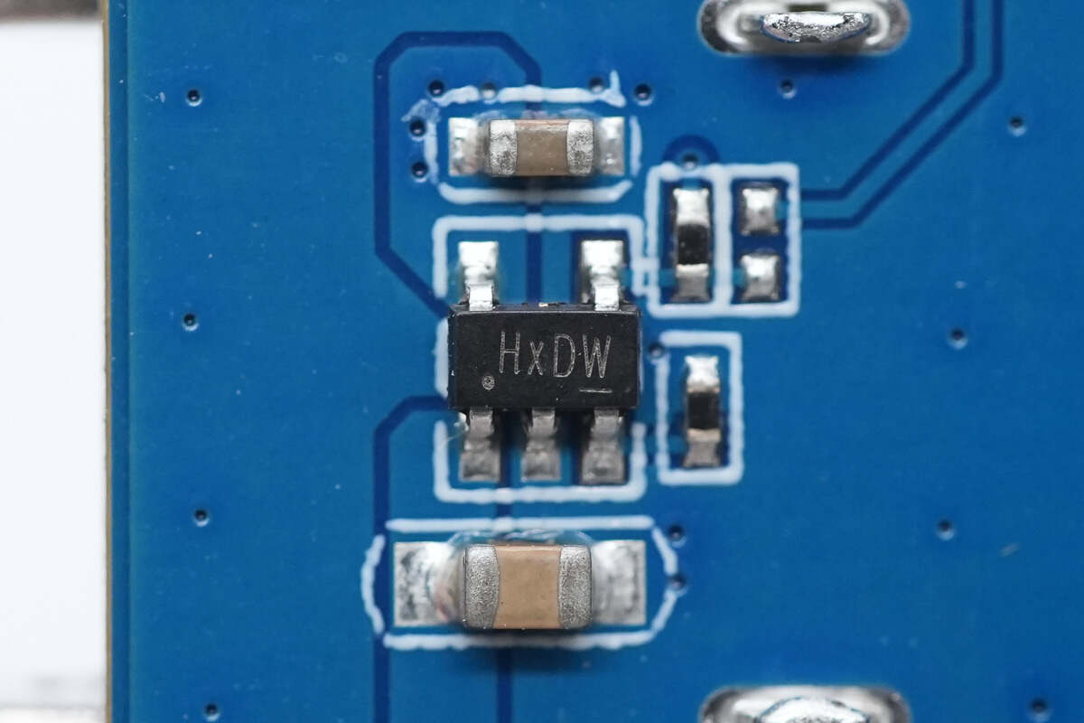
The buffer is from TI, marked with H17R, model SN74AUP1G17. It features a Schmitt-trigger input and comes in an SOT-23 package.
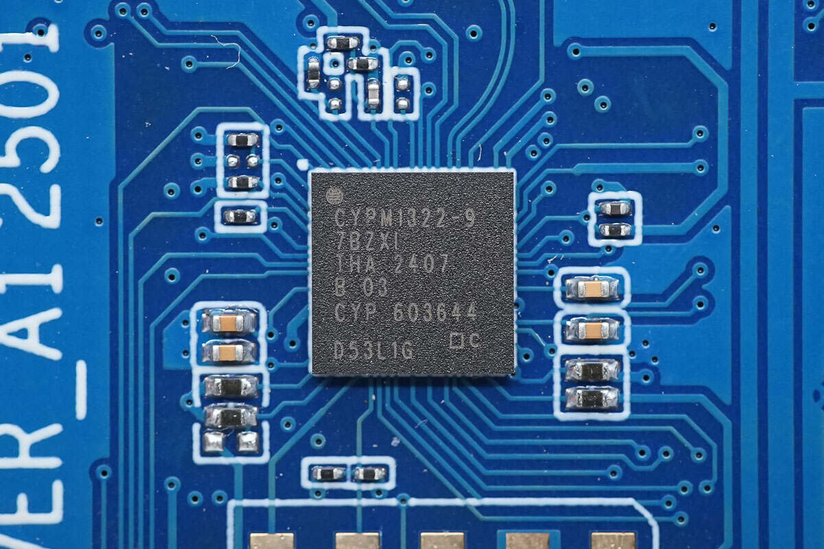
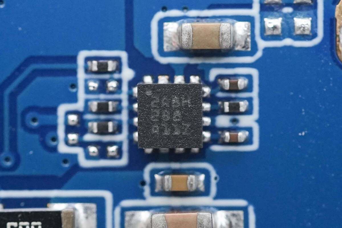
The USB-C controller is from Infineon, model CYPM1322-97BZXI, part of the EZ-PD PMG1-S3 series high-voltage microcontroller chips. It features a built-in ARM Cortex-M0+ MCU, 256KB Flash, and 32KB SRAM. The chip integrates voltage regulators and protection circuits and comes in a 97-BGA package.
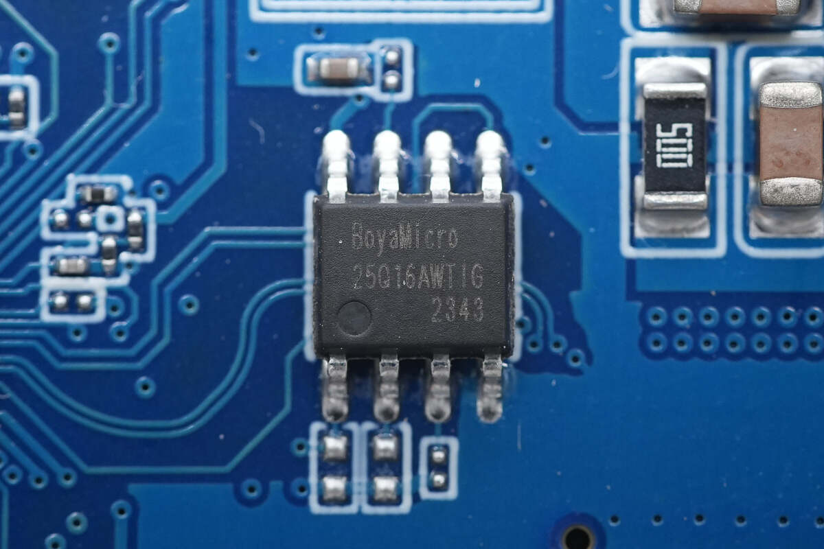
The memory is from BoyaMicro, model BY25Q16AWTIG, with a capacity of 2MB, packaged in SOP8.
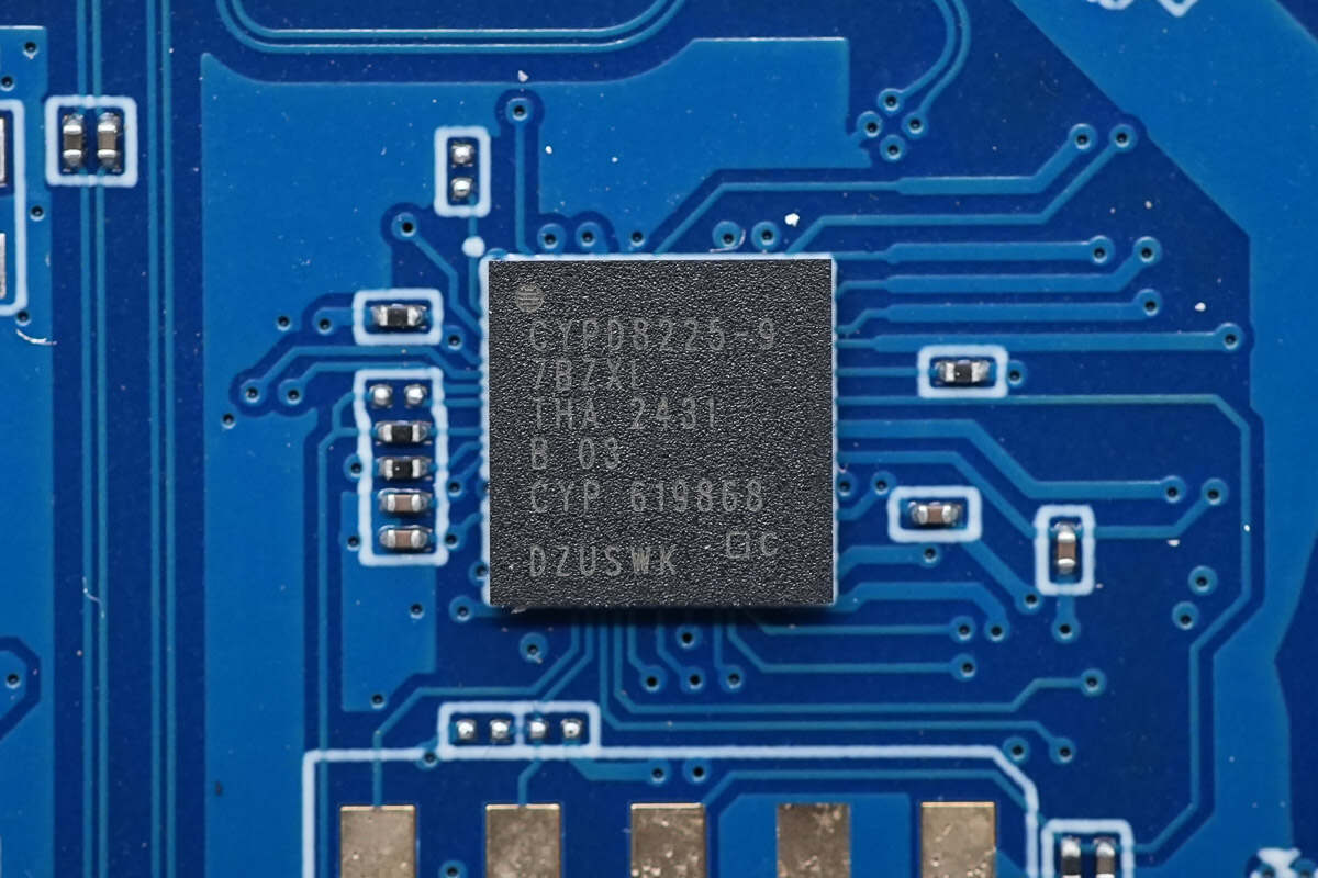
The other USB-C controller is from Infineon’s EZ-PD CCG8 series, model CYPD8225-97BZXI. This chip supports PD3.1 28V EPR applications, features a built-in ARM Cortex-M0+ MCU, 256KB Flash, and 32KB SRAM. It supports dual-port control and comes in a 97-BGA package.
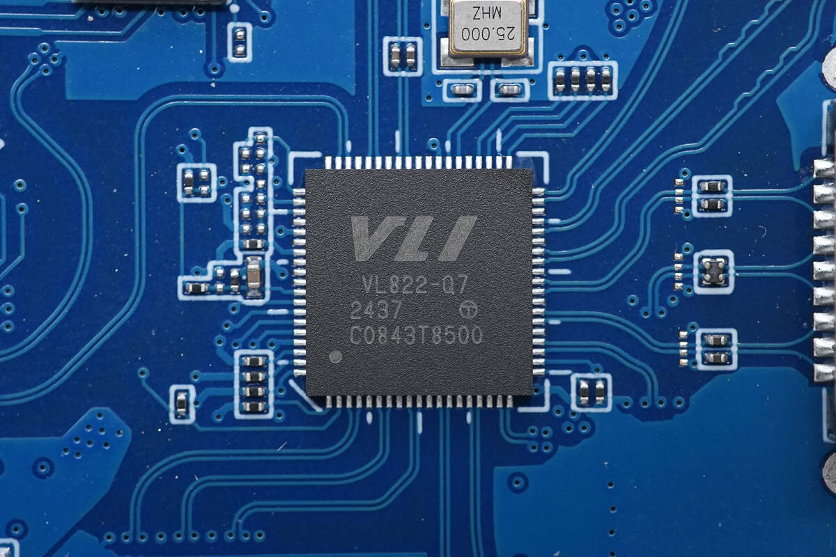
The USB hub chip is from VIA Labs, model VL822-Q7. It integrates an upstream port and two downstream port multiplexers, suitable for expanding four USB-A ports. It supports 10Gbps speeds and comes in a QFN-76 package.
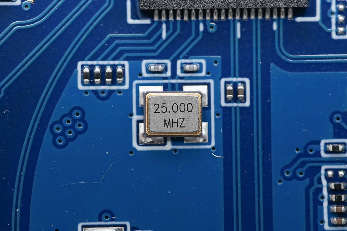
Close-up of the external 25.000 MHz clock crystal oscillator.
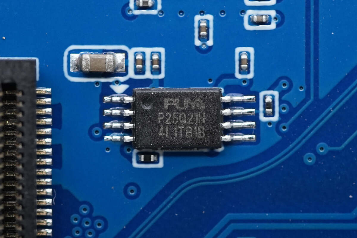
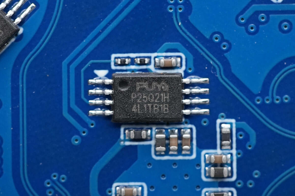
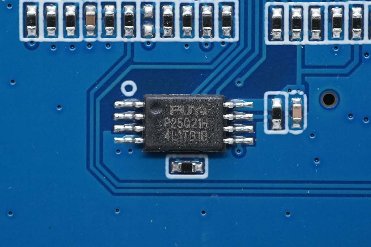
The memory is from Puya, model P25Q21H, with a capacity of 256KB, packaged in TSSOP8.
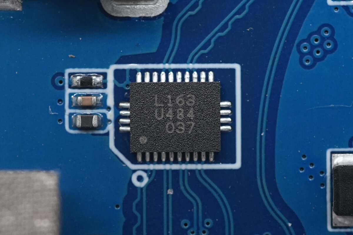
The VIA Labs VL163 port multiplexer is used for switching the front and back of the USB-C interface and comes in a QFN-28 package.
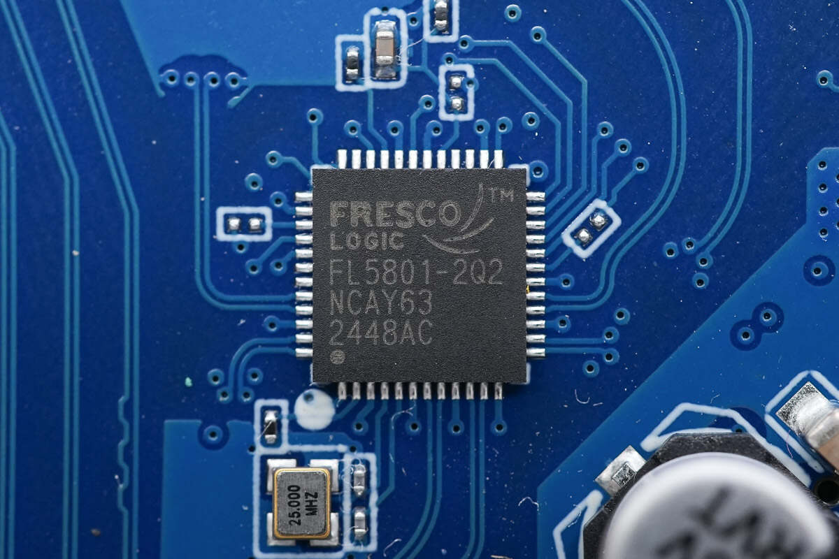
The hub chip is from Parade Technologies, model FL5801-2Q2. It is a USB 2.0 hub supporting configurations of 1 upstream port with 5 downstream ports, and 2 upstream ports with 4 downstream ports. It is backward compatible with USB 1.1, supports the BC1.2 specification, and allows for feature customization. The chip comes in a QFN48 package.
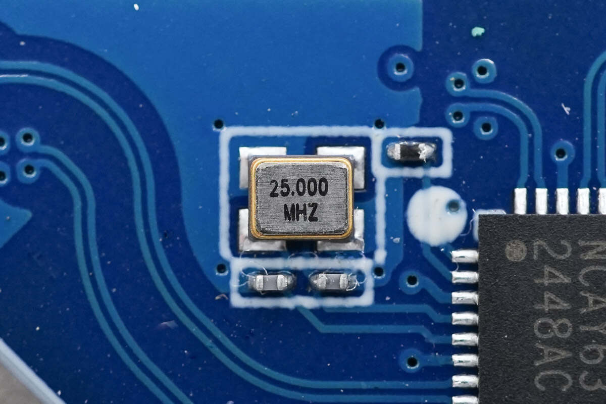
Close-up of the external 25.000 MHz clock crystal oscillator.
The memory is from Puya, model P25Q21H, with a capacity of 256KB, packaged in TSSOP8.
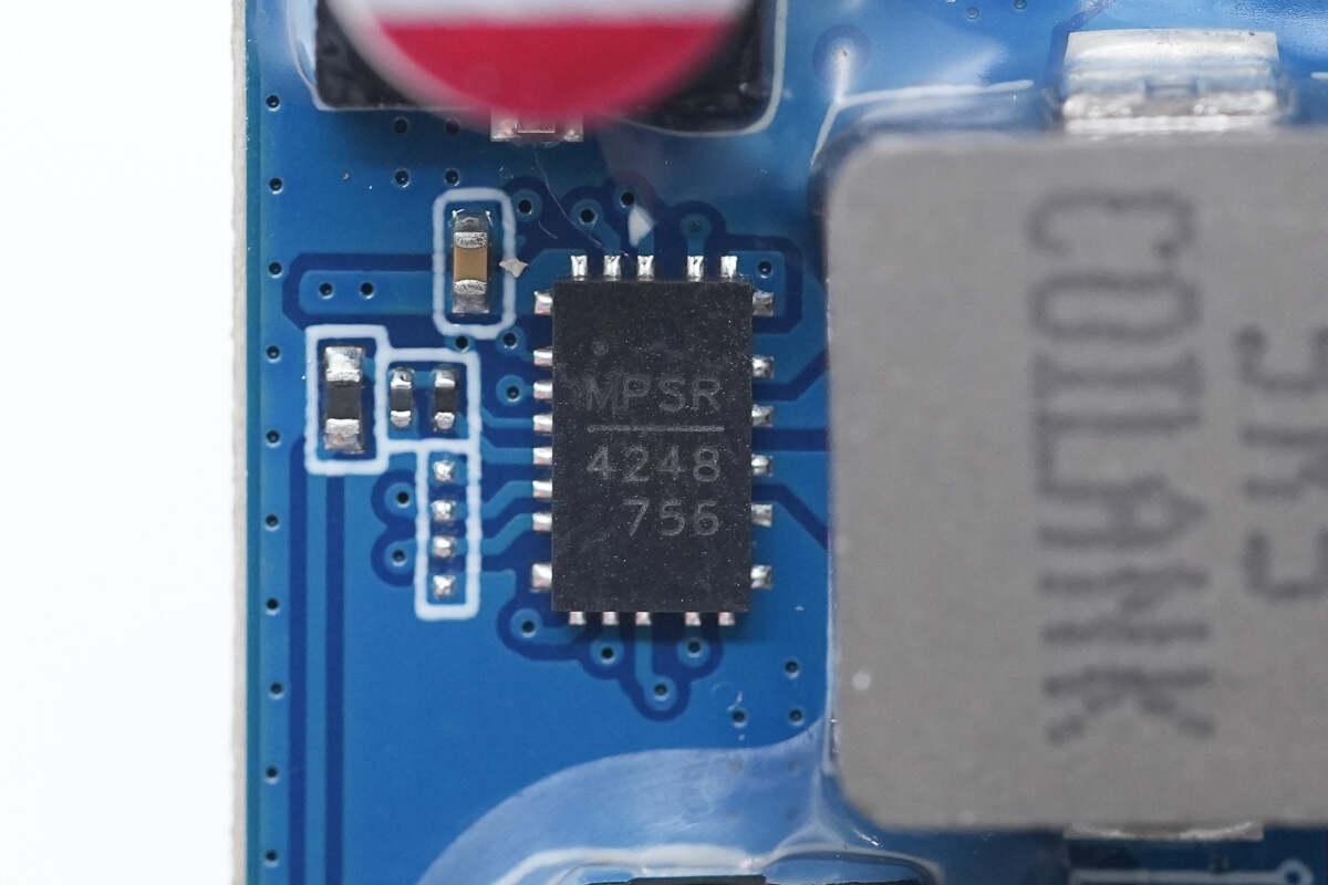
The synchronous buck-boost chip used for the Thunderbolt 5 upstream interface 140W output is from MPS, model MP4248. It is a synchronous buck-boost converter with two internal low-side MOSFETs and an integrated external PMOSFET driver. The chip supports 140W output power, 36V input and output voltage, and can connect to the protocol chip via an I2C interface. It comes in a QFN 3x5-20 package.
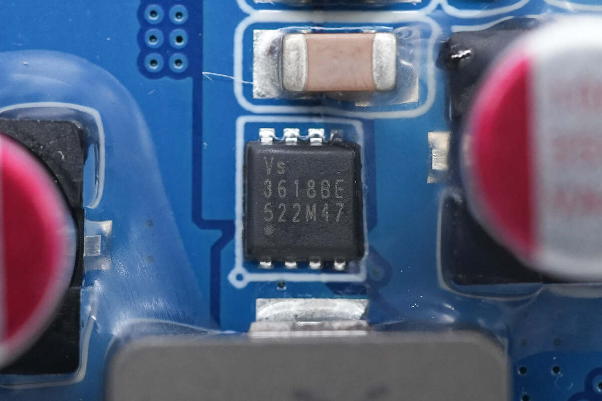
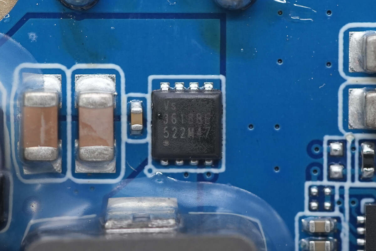
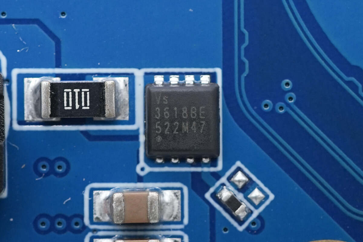
The external MOSFET is from Vergiga, model VS3618BE. It is an NMOS with a voltage rating of 30V and an on-resistance of 5.2mΩ, packaged in PDFN3333.
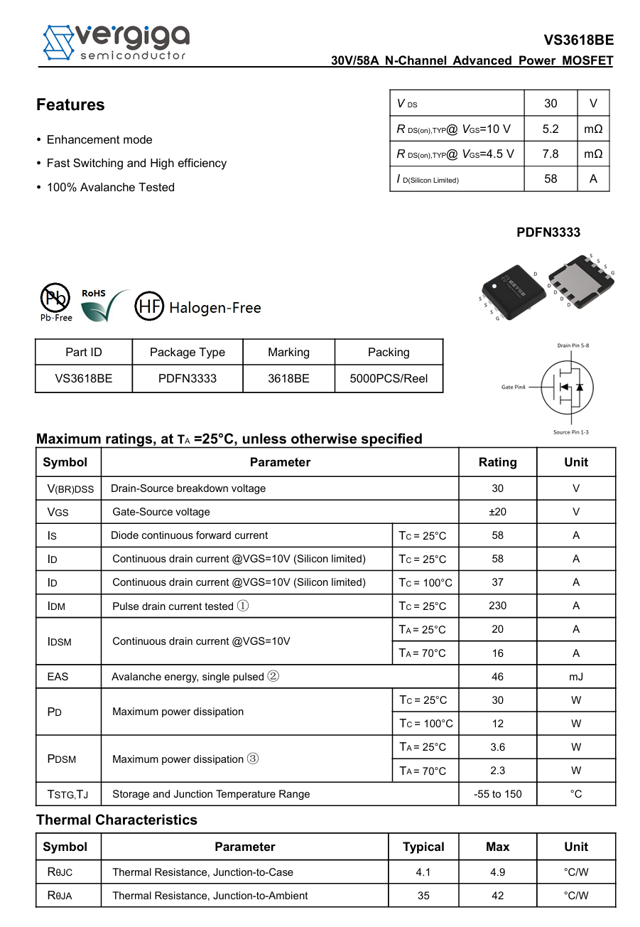
Here is the information about Vergiga VS3618BE.
The other MOSFET has the same model.
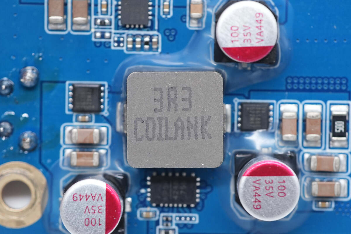
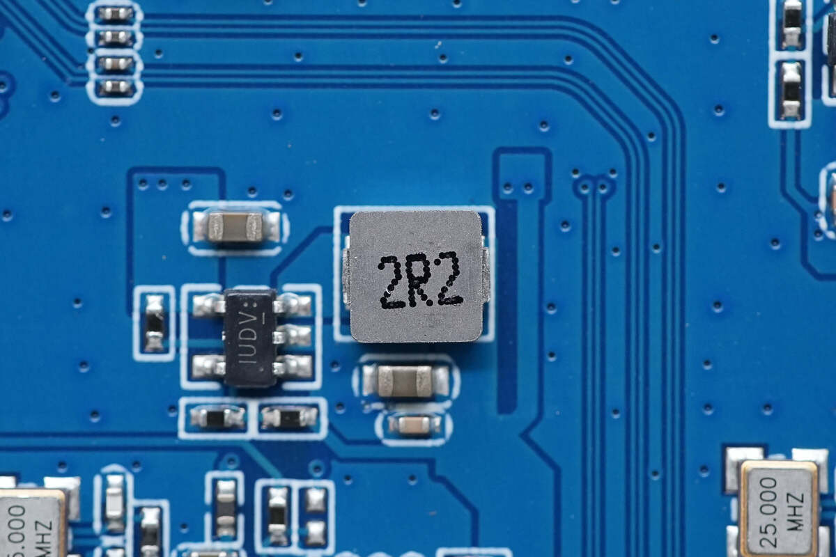
The alloy inductor is from Coilank, rated at 3.3μH, with glue reinforcement applied at the bottom.
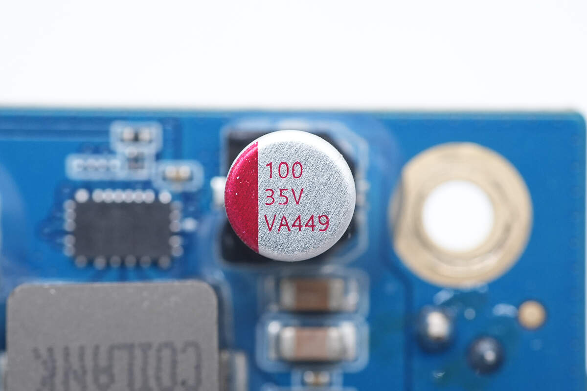
The filter capacitor is from PolyCap, a VA series high-voltage chip capacitor, rated at 100μF 35V.
The other filter capacitor has the same specifications.
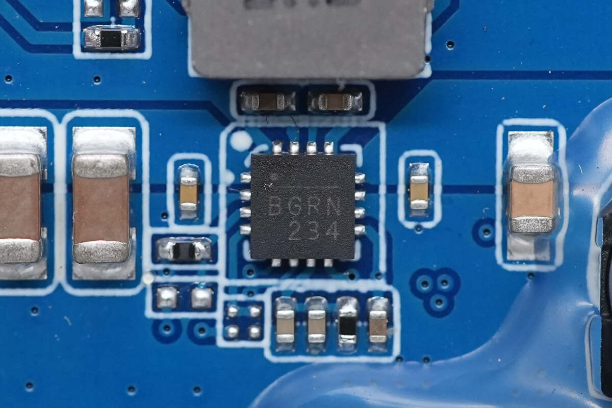
The synchronous buck-boost converter from MPS, marked with BGR and model MP8859, integrates internal MOSFETs and supports an input voltage of up to 22V. It provides an output current of 3A and features an adjustable constant current limit. The device includes output overvoltage protection, overcurrent protection, and short-circuit protection. It is packaged in a QFN16 package.
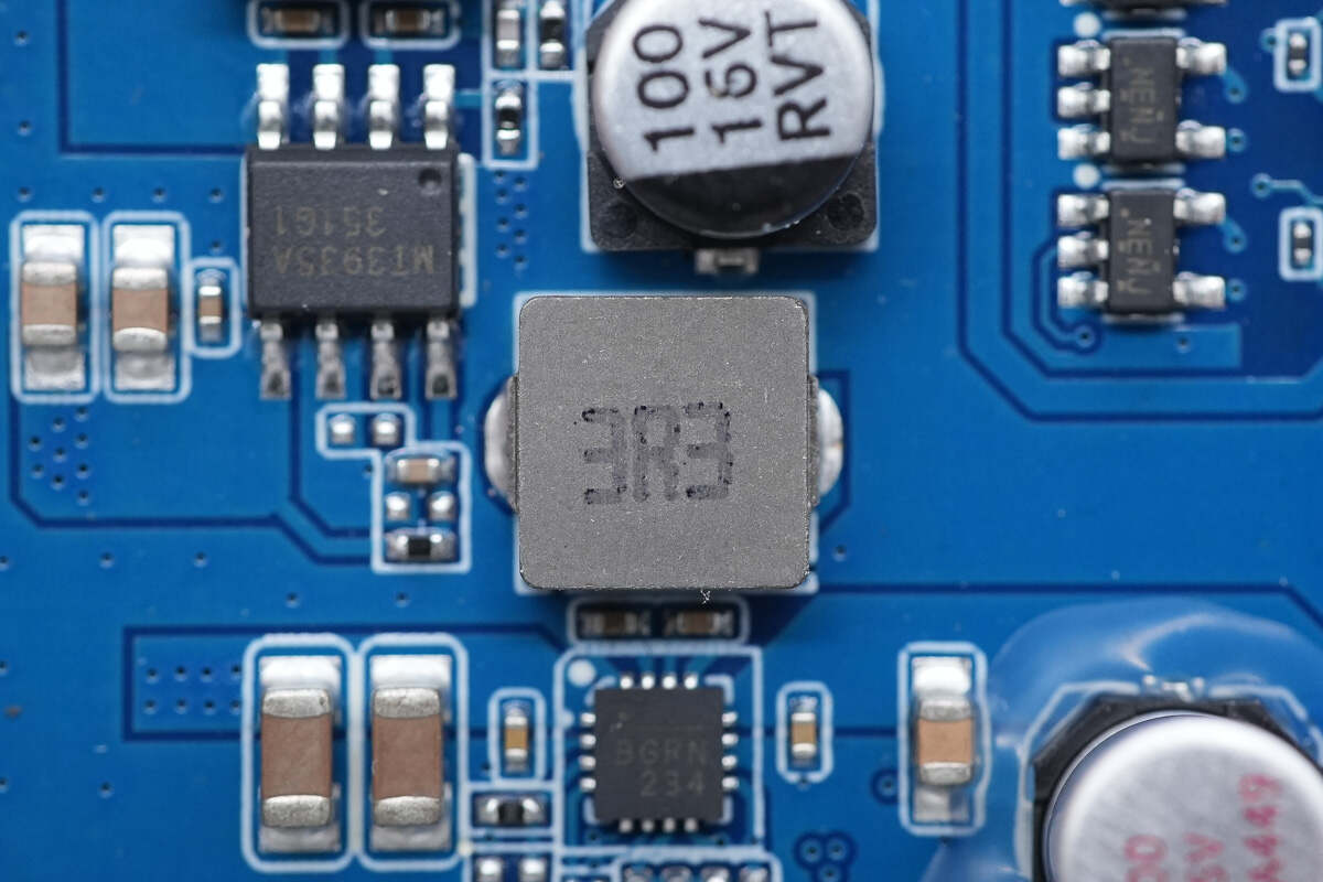
Close-up of 3.3μH alloy inductor.
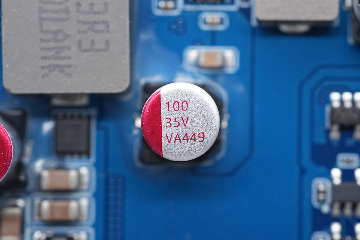
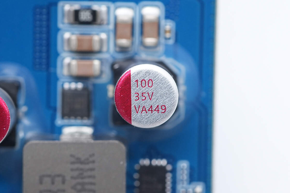
The filter capacitor is rated at 100μF 35V.
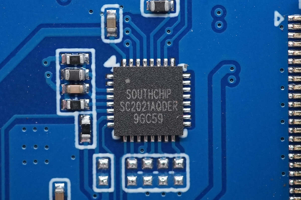
The protocol chip used is the SouthChip SC2021A, a highly integrated Type-C/PD and DPDM fast charging controller. It complies with the latest Type-C and PD 3.0 standards and has passed the USB PD 3.1 compliance test. The chip supports proprietary high-voltage fast charging protocols and includes one USB-C interface and two DPDM interfaces, making it suitable for 1A+1C dual-port fast charging applications. It comes in a QFN32 package.
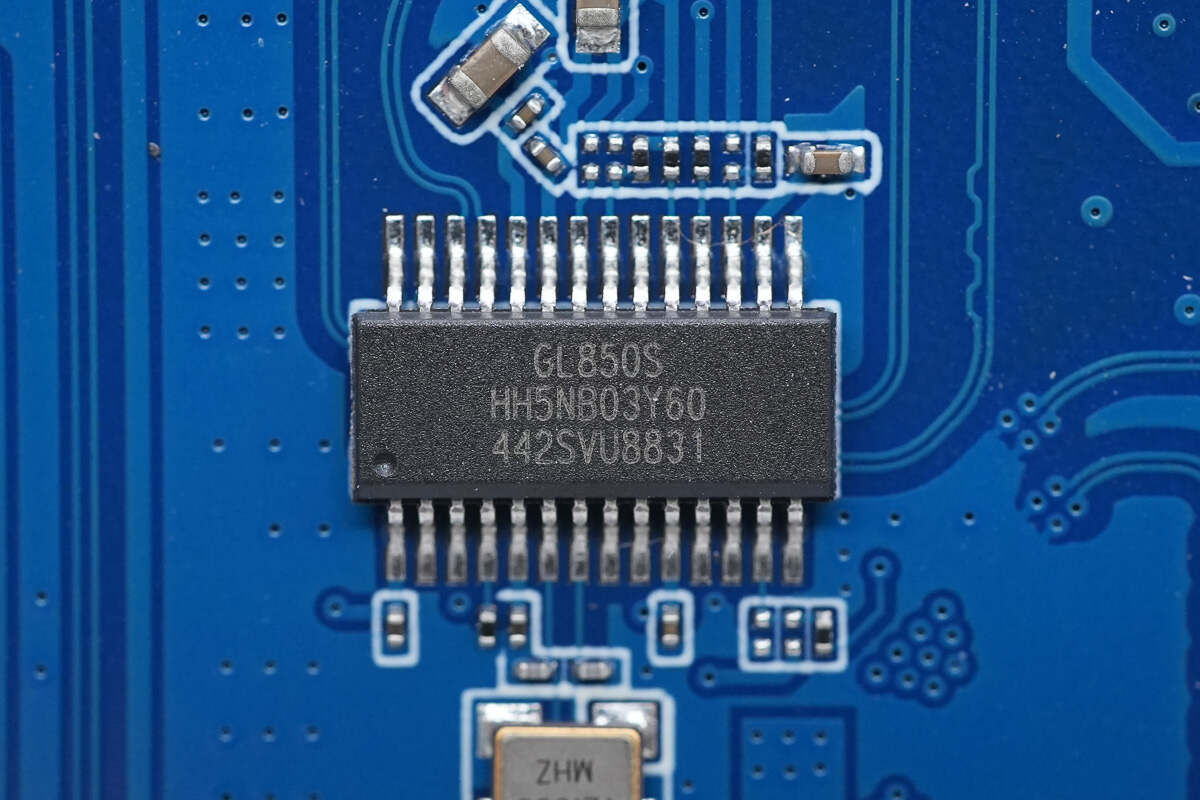
The USB hub chip is from GENESYS, model GL850G. It is a four-port USB 2.0 HUB chip and comes in an SSOP28 package.
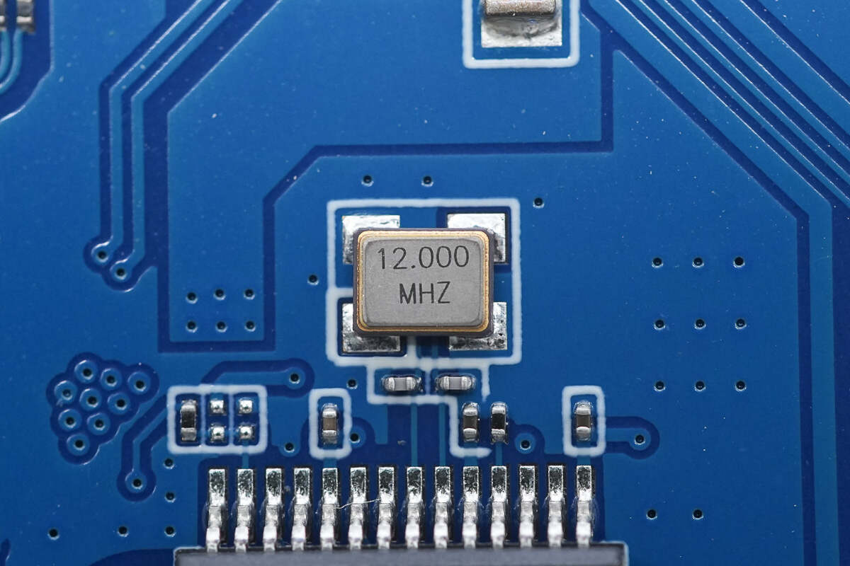
Close-up of external 12.000 MHz crystal oscillator.
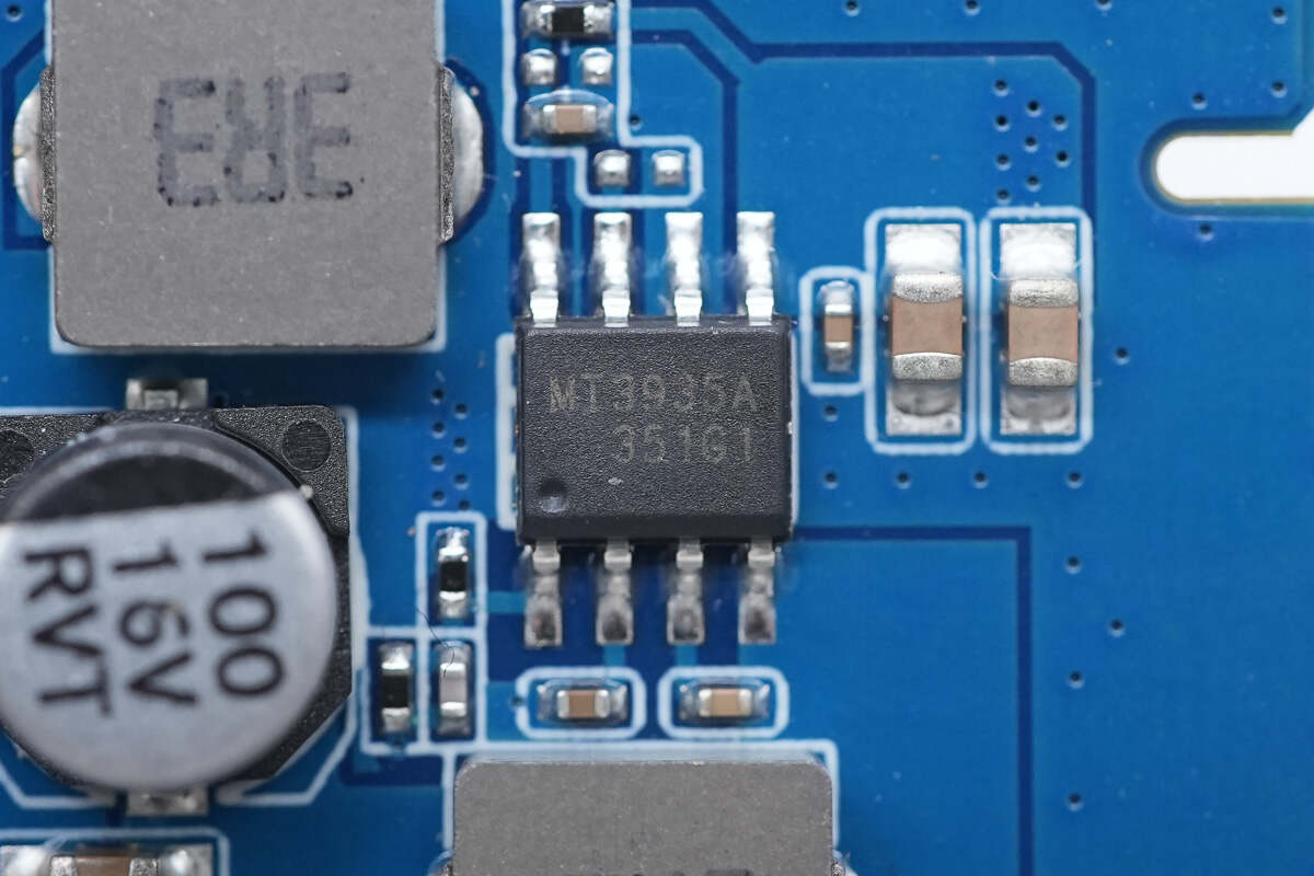
The synchronous buck converter chip is from M3TEK, model MT3935A. It supports an input voltage of 26V, a continuous output current of 4A, and a peak output current of 5A. The chip integrates MOSFETs and is packaged in an SOP8-EP package.
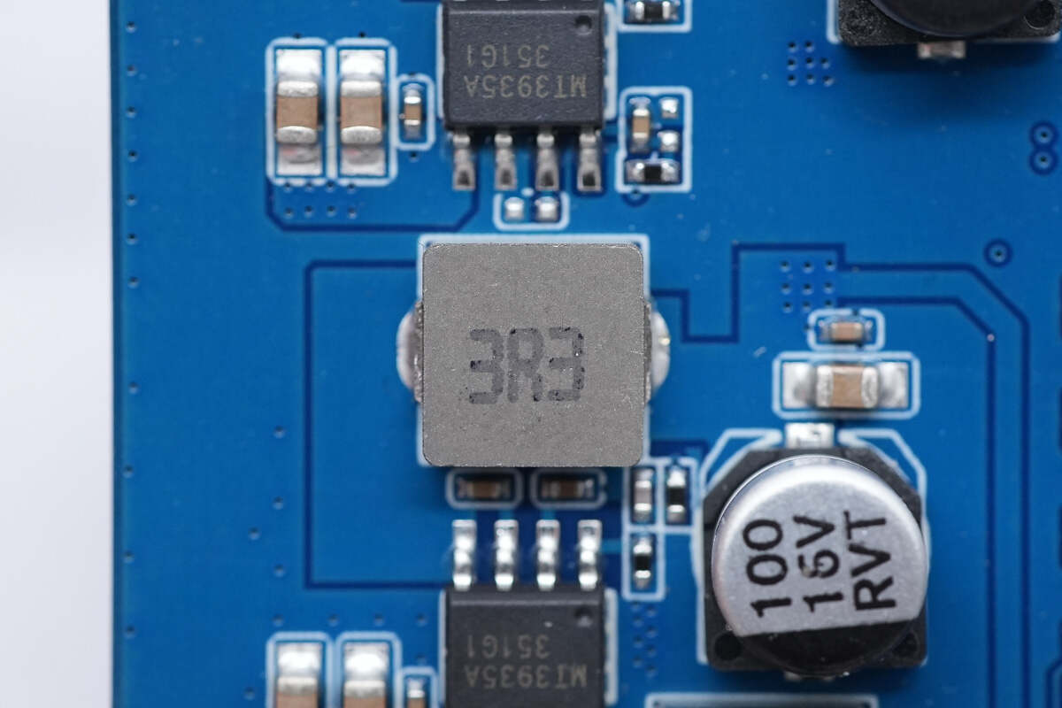
Close-up of 3.3μH alloy inductor.
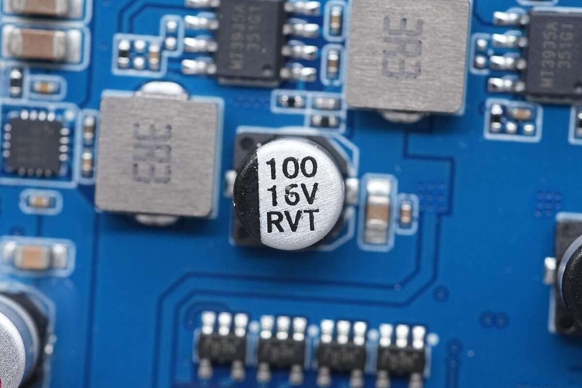
The electrolytic capacitor is rated at 100μF 16V. There are a total of five identical buck circuits on the PCB, which will not be described further to save space.
The VBUS MOSFET used is the Vergiga VS3618BE.
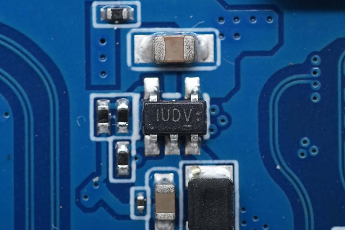
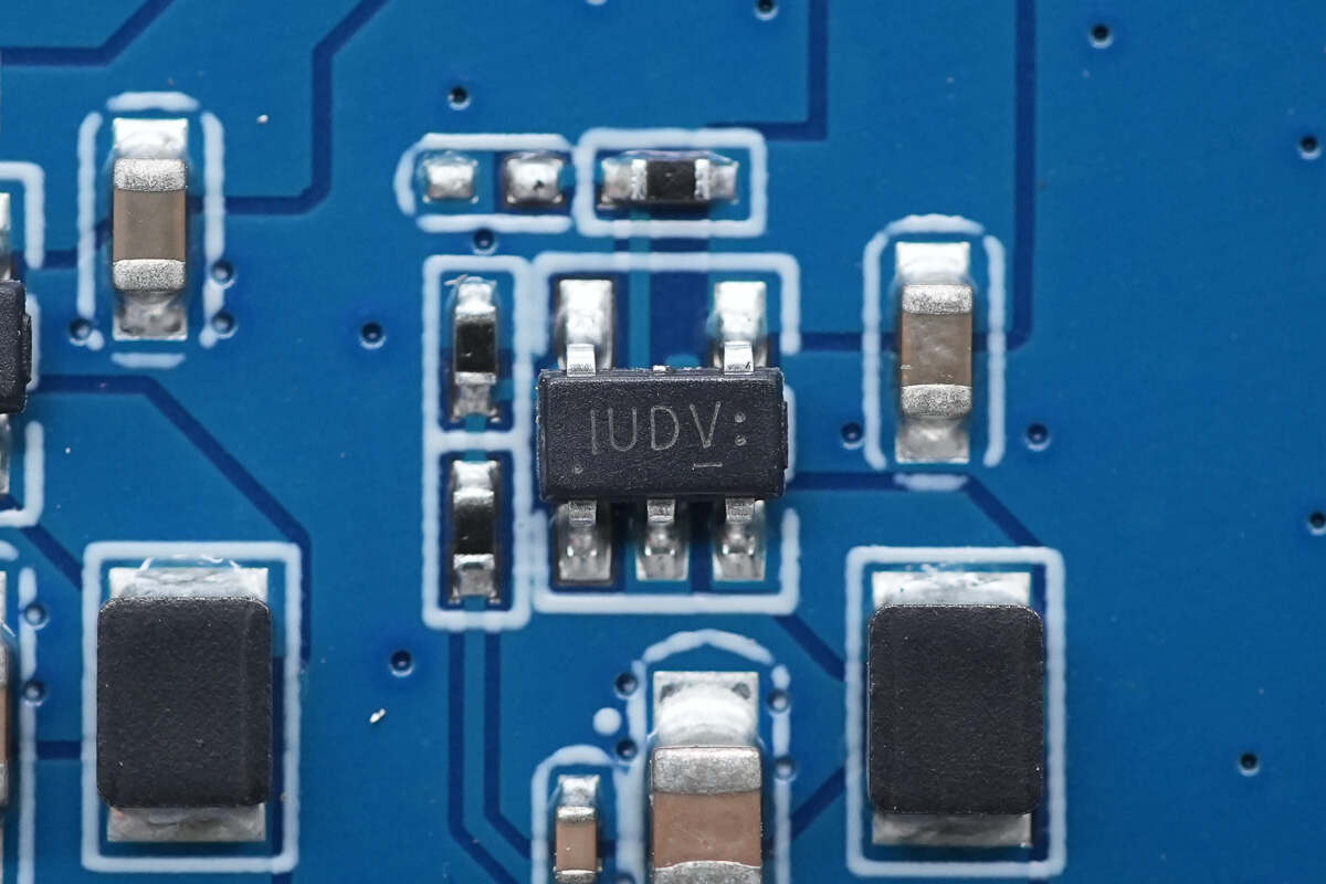
The synchronous buck converter is from ETA, marked with IU, model ETA3485S2F. It supports a 7V input voltage, adjustable output voltage, and an output current of 1.5A, with a switching frequency of 2MHz. Fixed output voltage versions of 1.2V, 2.5V, and 3.3V are also available. It comes in a SOT23-5 package.
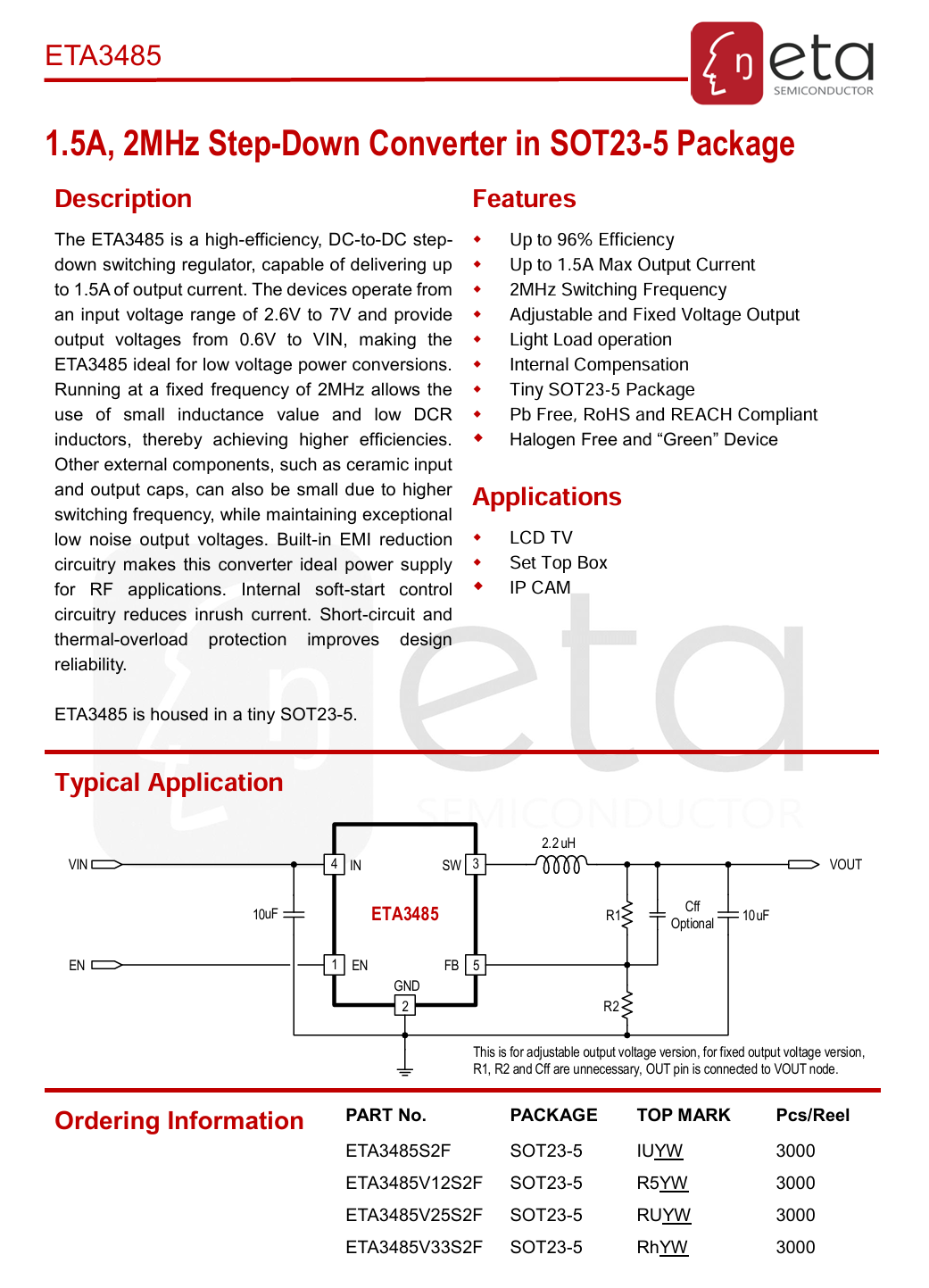
Here is the information about ETA ETA3485.
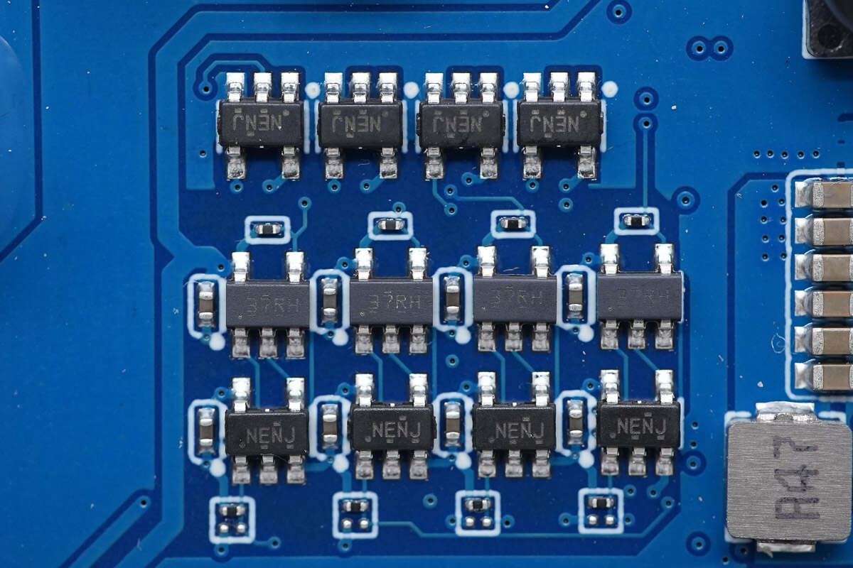
Four buffer gate chips are from TI, marked with 37RH, model SN74LV1T125, featuring tri-state outputs. Eight buffer gate chips are marked with NENJ, model SN74LV1T126, also featuring tri-state outputs. All are in SOT23 packages.
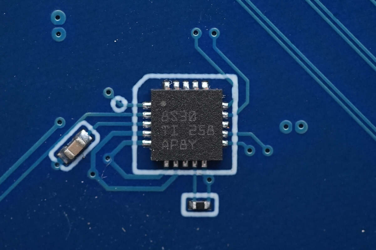
The USB-C port protector is from TI, marked with 8S30, model TPD8S300. It provides 4-channel VBUS short-to-overvoltage protection and 8-channel ESD protection. It comes in a WQFN20 package.
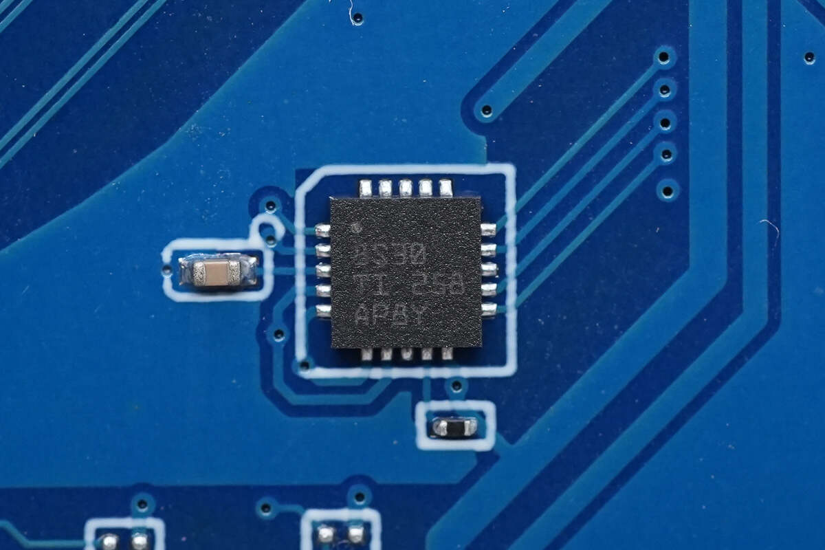
The other USB-C port protector is of the same model.
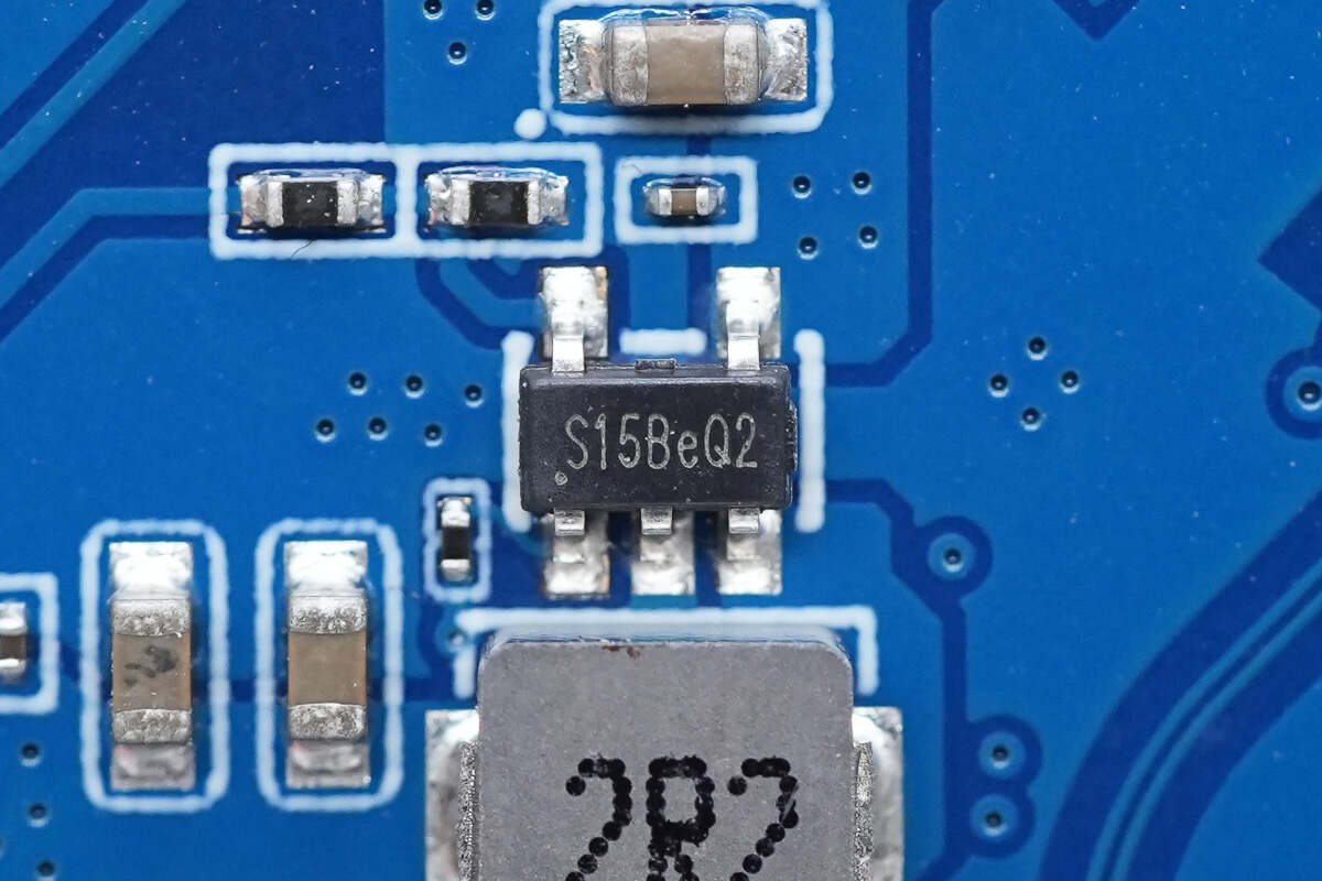
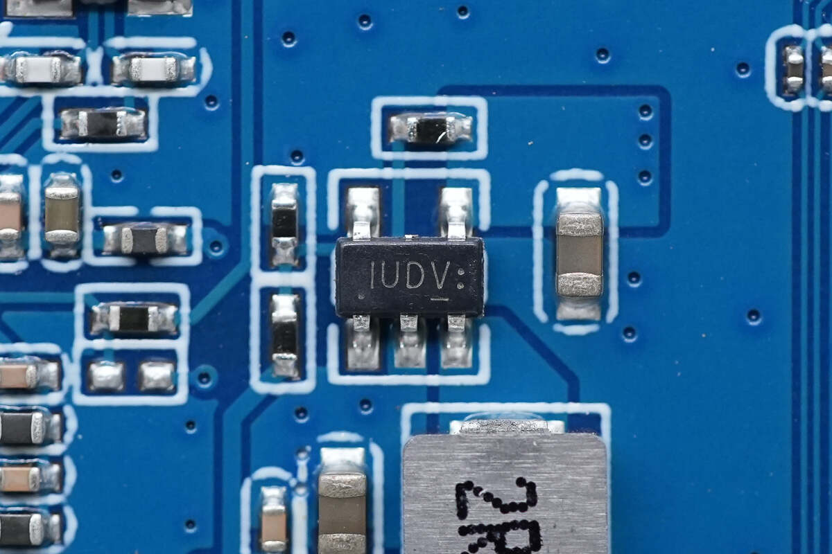
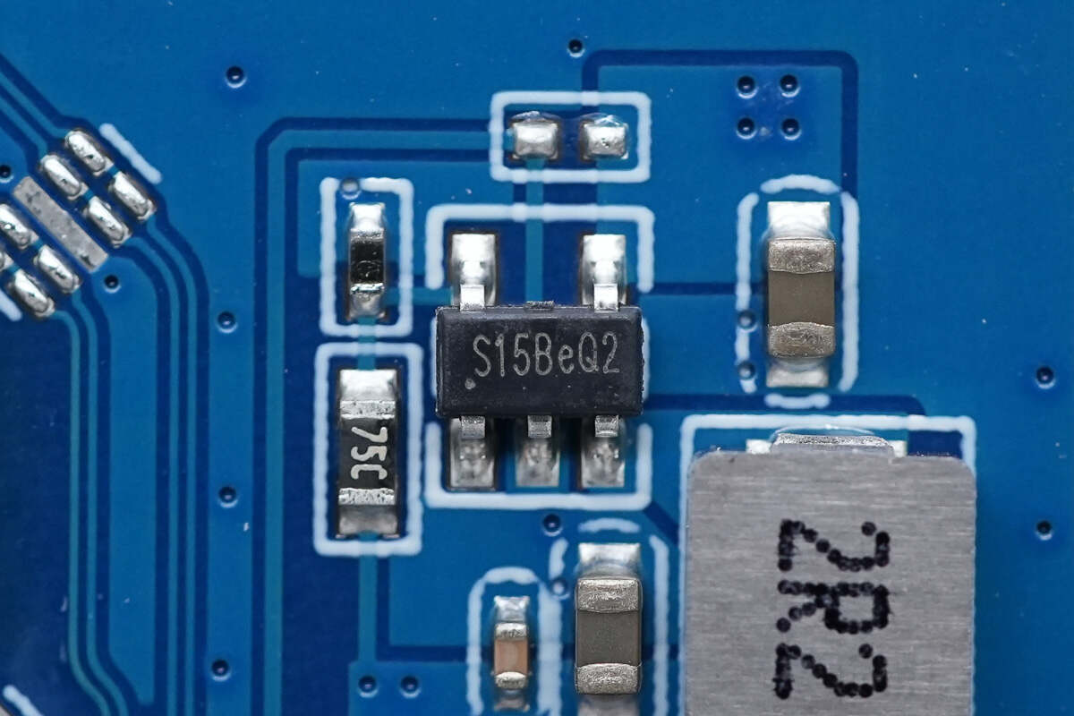
The synchronous buck converter chip is from Tollsemi, marked with S15B, model TMI3410. It supports an input voltage of 5.5V and provides an output current of 1.2A, with a switching frequency of 1.5MHz. The chip features input overvoltage protection, short-circuit protection, and overtemperature protection. It comes in a SOT23-5 package.
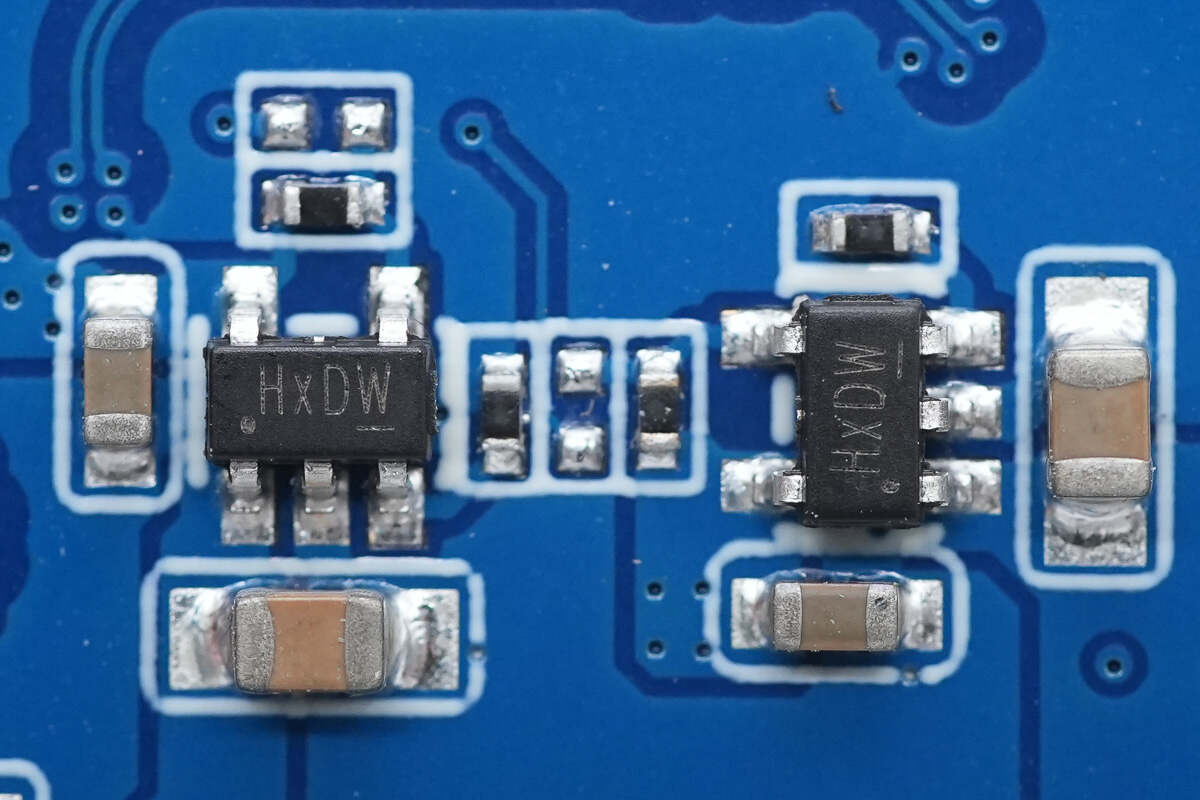
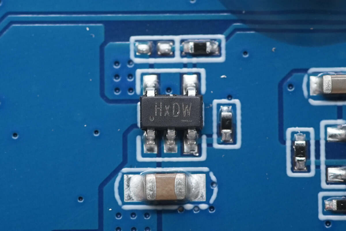
Two overcurrent protection chips are from ETA, marked with Hx, model ETA6280S2F. They support an input voltage range of 2.1–6V and feature 6.1V overvoltage protection. The output current can be set via an external resistor, with a configurable range of 75mA to 2.2A. The chips offer fast overcurrent response and support reverse current blocking. They come in a SOT23-5 package.
Here is the information about ETA ETA6280.
The overcurrent protection chip is from TI, marked with 2ABH, model TPS259472. It supports an operating voltage of 23V and an operating current of 6A. The overvoltage clamp threshold and overcurrent protection threshold are configurable. It features adjustable output slew rate control and includes overtemperature protection. The chip is certified under IEC 62368-1 CB and comes in a 2×2 mm QFN package.
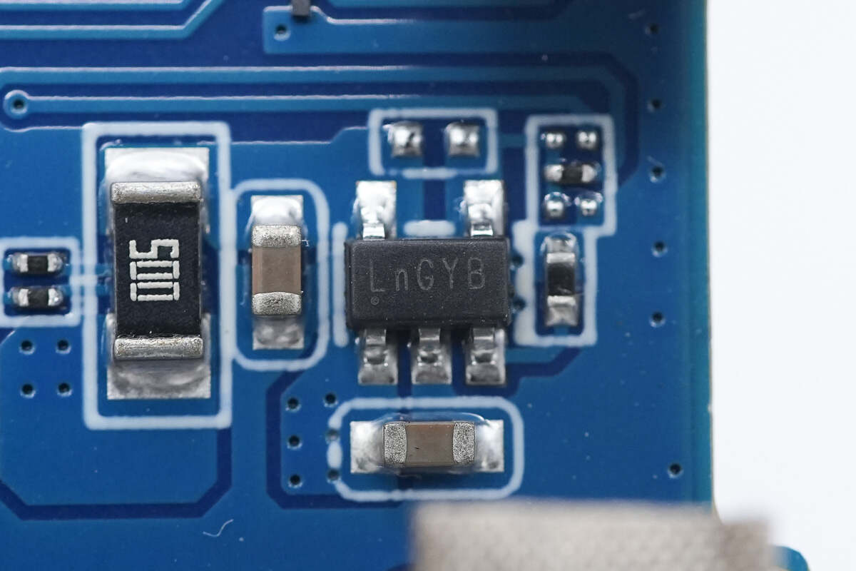
The overcurrent protection chip is marked with Ln and comes in a SOT23-5 package.
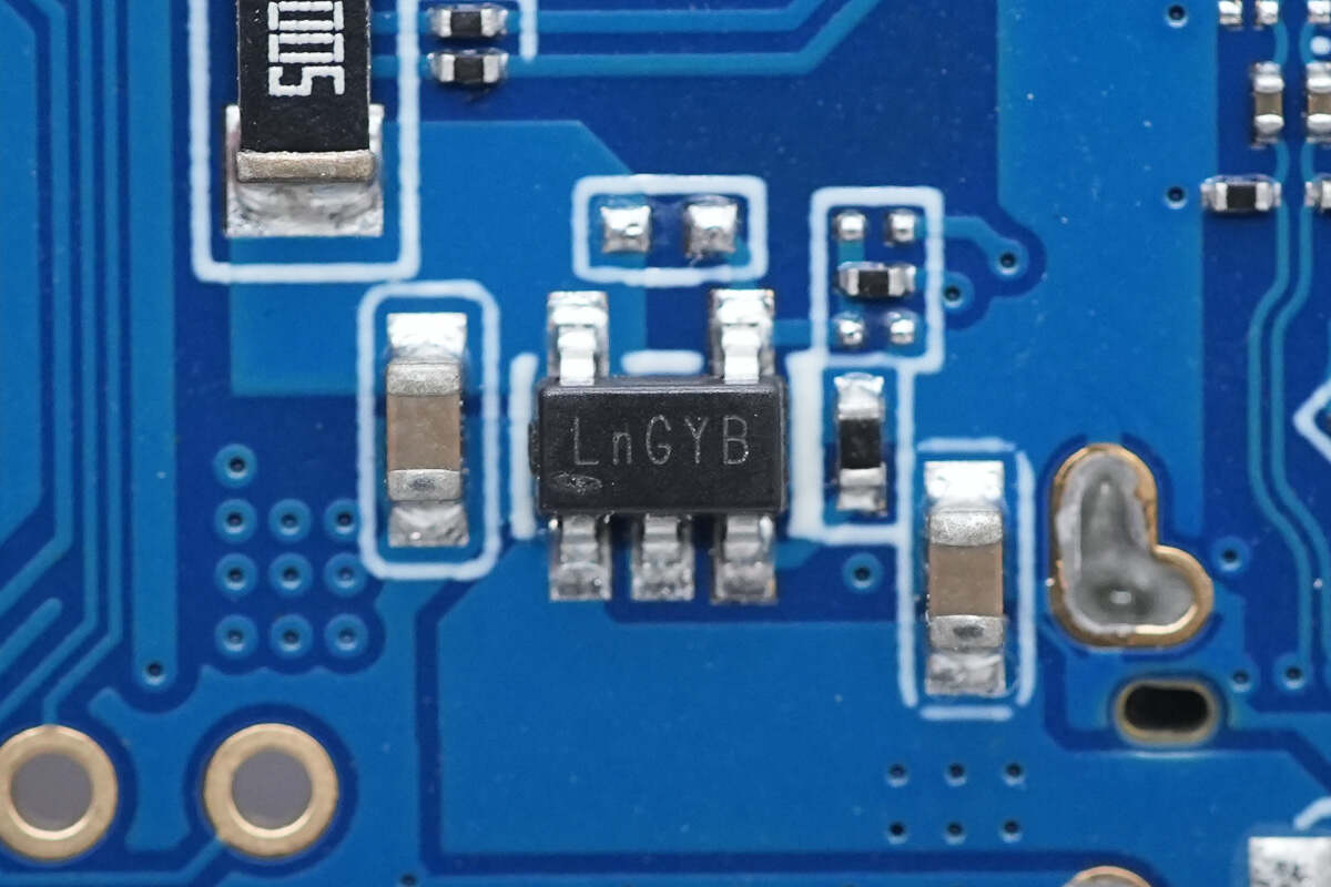
The other overcurrent protection chip is marked with the same code.
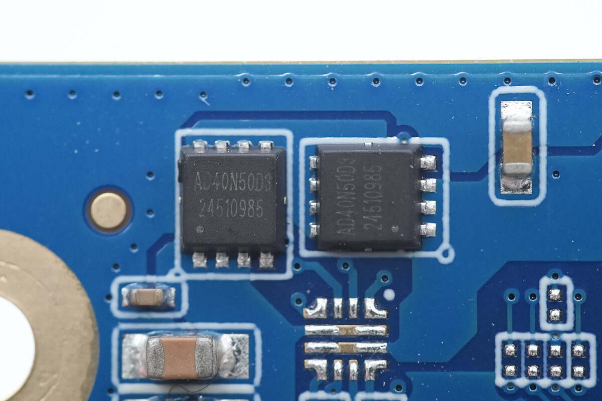
The VBUS MOSFET used for the Thunderbolt 5 upstream interface is from ADAMANT, model AD40N50D3. It is an NMOS with an on-resistance of 4.5mΩ and a voltage rating of 40V. It comes in a PPAK 3×3 package.
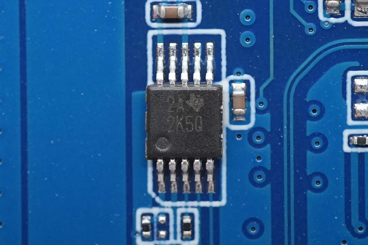
The digital power monitor is from TI, marked with 2K5Q, model INA230. The chip supports a 36V bus voltage and high-side or low-side sensing. It provides current, voltage, and power reporting, and comes in a VSSOP10 package.
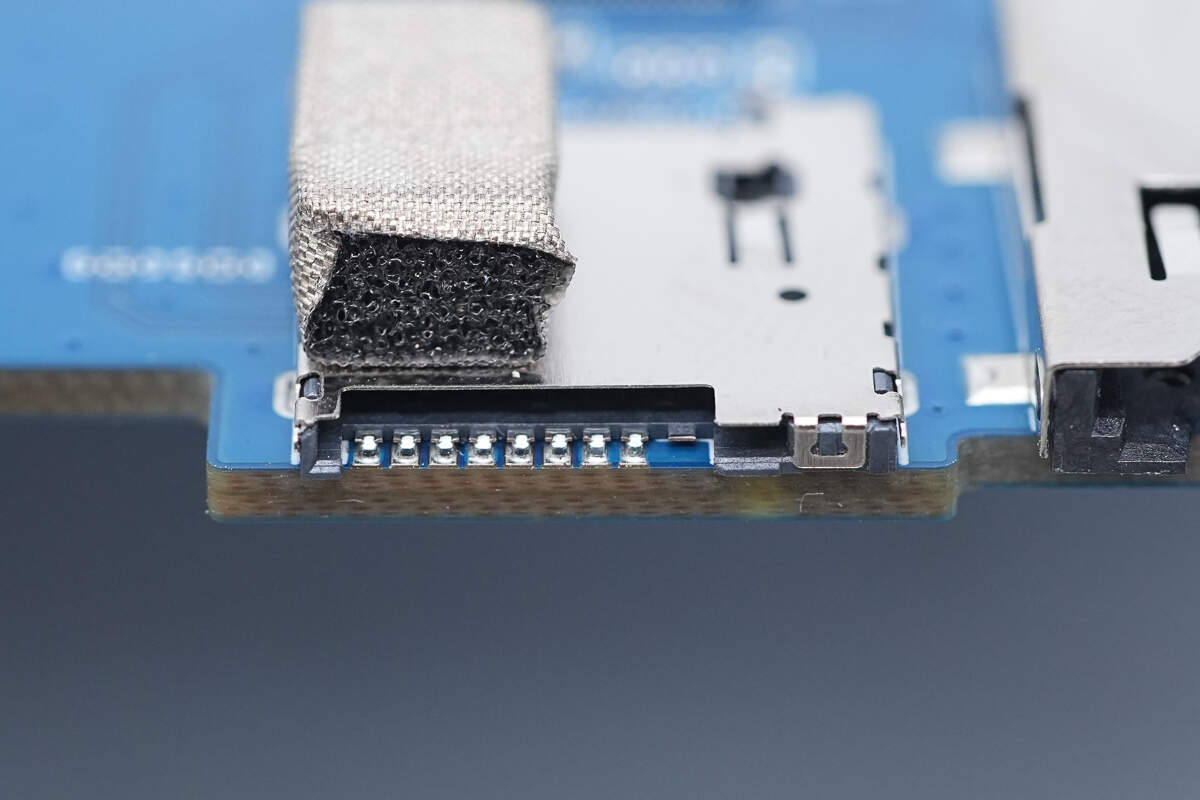
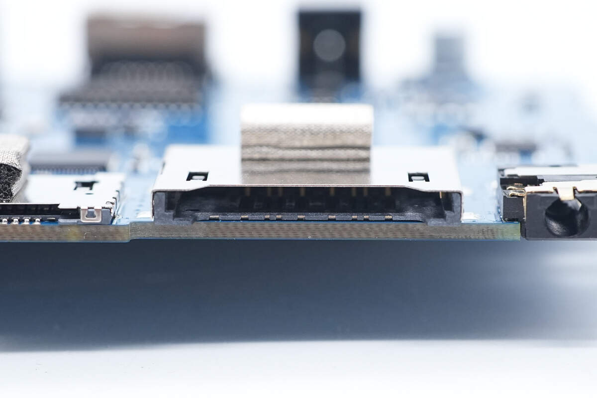
Close-up of the connector used to connect two PCBs.
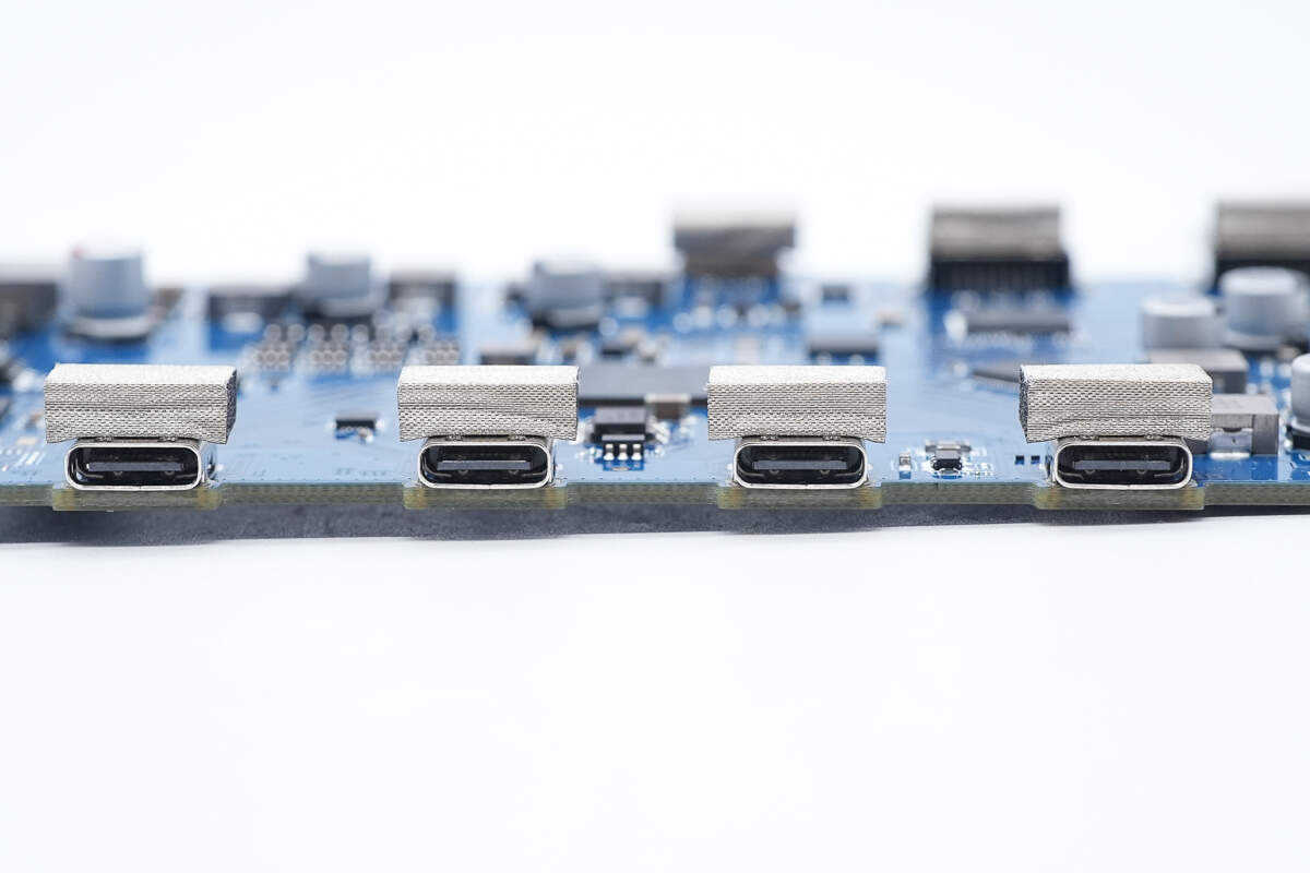
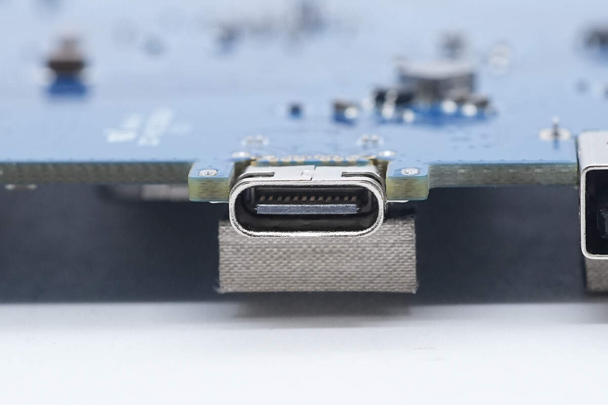
The USB-C sockets are secured by through-hole soldering and grounded with adhesive conductive fabric.
The USB-C socket on the front panel uses flush-mount soldering.
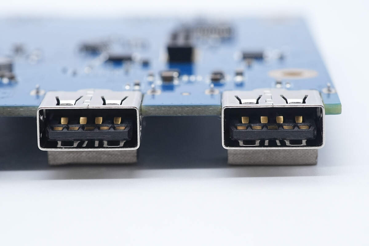
The USB-A sockets also use flush-mount soldering.
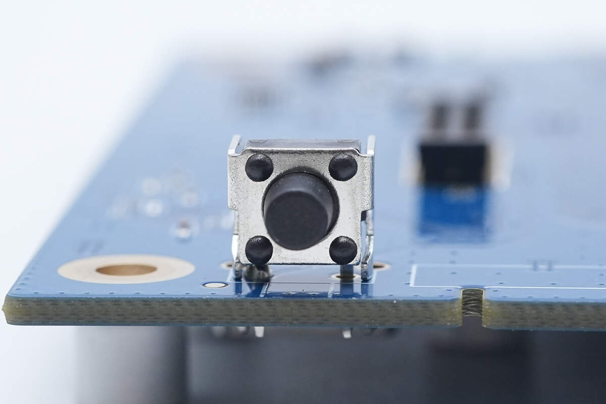
The power button is secured by through-hole soldering.
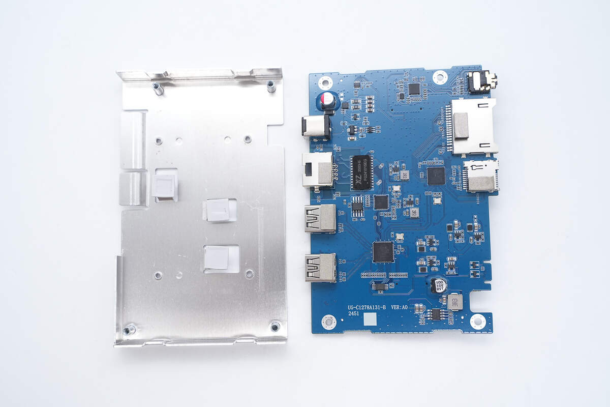
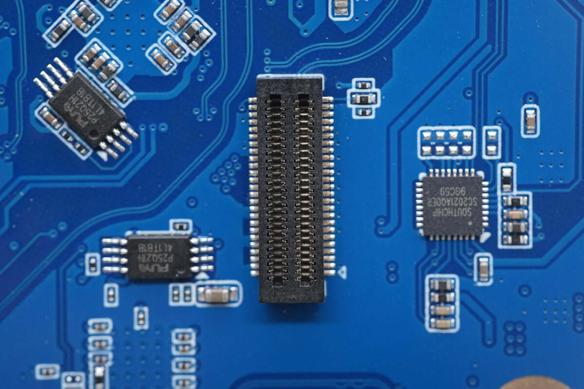
The lower PCB features a power socket, an Ethernet port, and two USB-A ports. The upper side includes a headphone jack, an SD card slot, and a TF card slot. In the middle are a hub chip, an Ethernet controller, and a card reader controller, while the left side houses the audio interface chip.
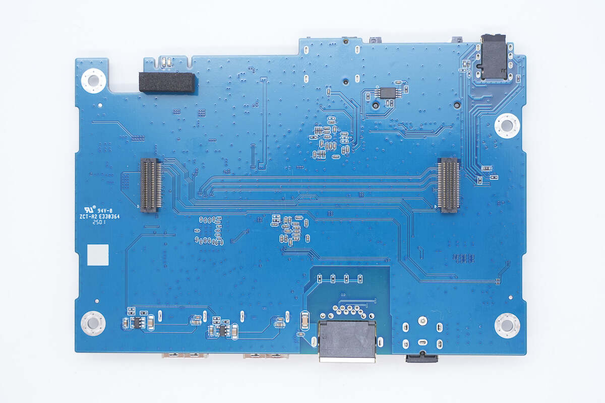
On the back are connectors, memories, and overcurrent protection chips.
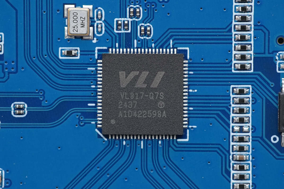
The USB hub chip is from VIA Labs, model VL817-Q7S. It is a 5G-rate hub chip used for USB interface expansion and comes in a QFN76 package.
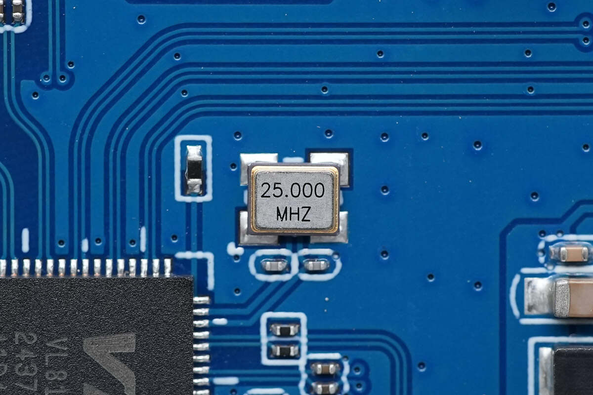
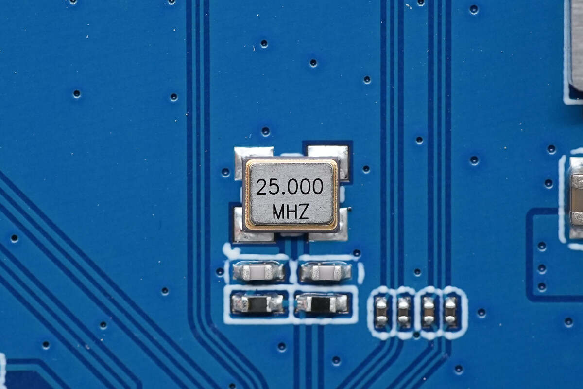
Close-up of the 25.000 MHz crystal oscillator.
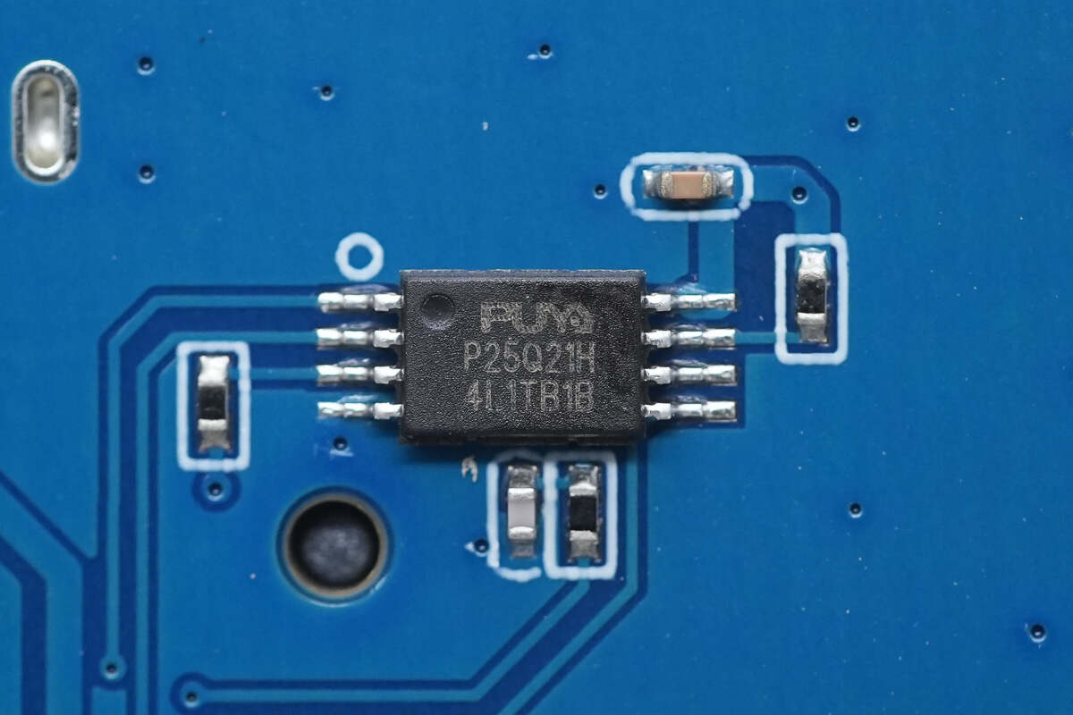
The memory is from Puya, model P25Q21H, with a capacity of 256KB. It comes in a TSSOP8 package.
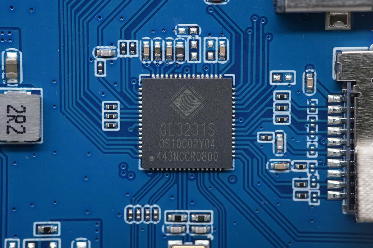
The card reader controller is from GENESYS, model GL3231S. It is a USB 3.1 Gen 1 card reader controller with an integrated DC-DC converter. The chip supports SD 3.0 UHS-1 and SD 4.0 UHS-2 memory cards and comes in a QFN64 package.
Close-up of the 25.000 MHz crystal oscillator.
The memory is from Puya, model P25Q21H, with a capacity of 256KB. It comes in a TSSOP8 package.
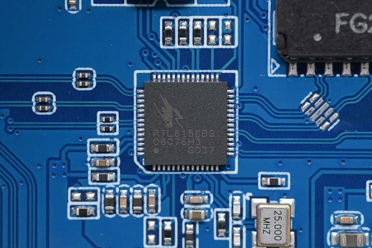
The 2.5G Ethernet controller is from REALTEK, model RTL8156BG. It is used for USB 3.0 to 2.5G wired networking and backward supports gigabit and 100Mbps speeds. It comes in a QFN56 package.
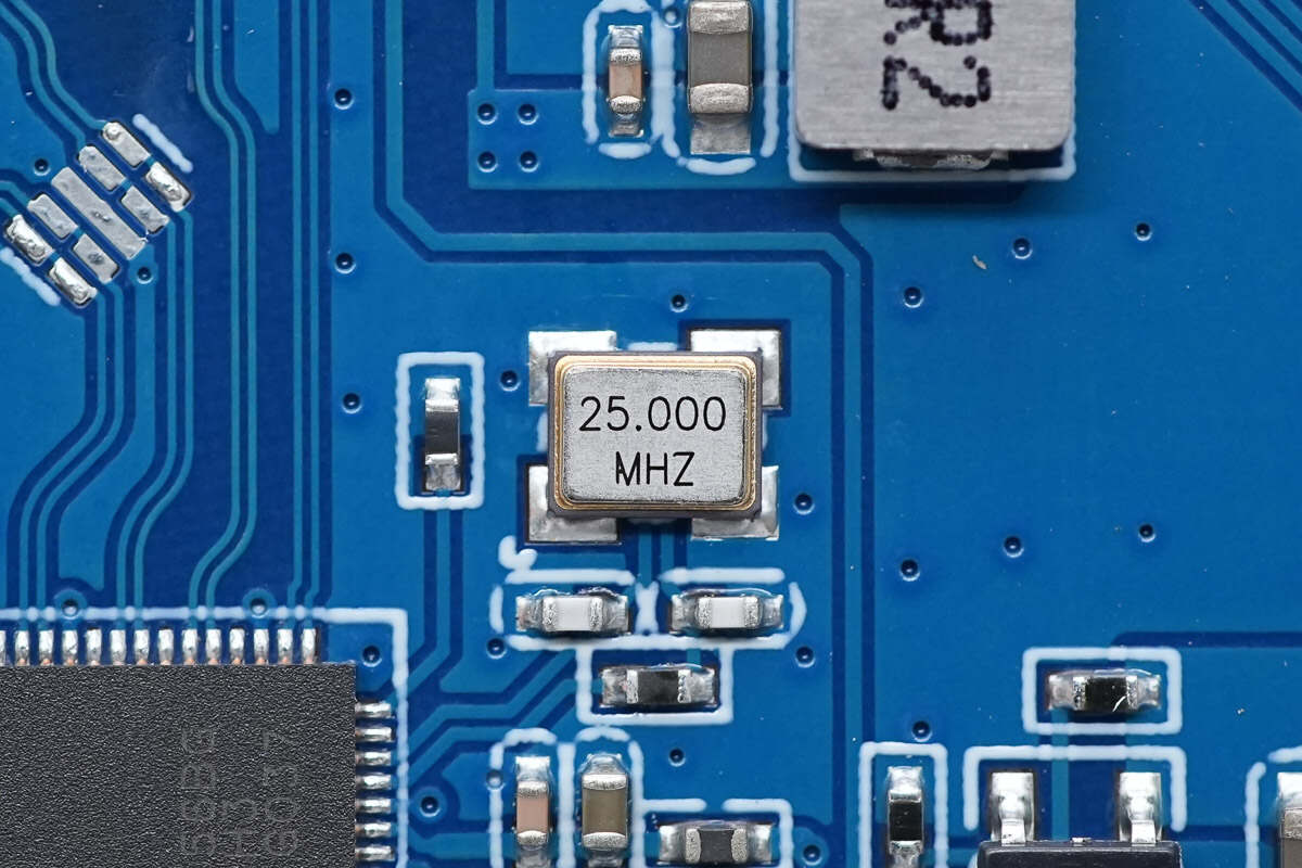
Close-up of the external 25.000 MHz crystal oscillator.
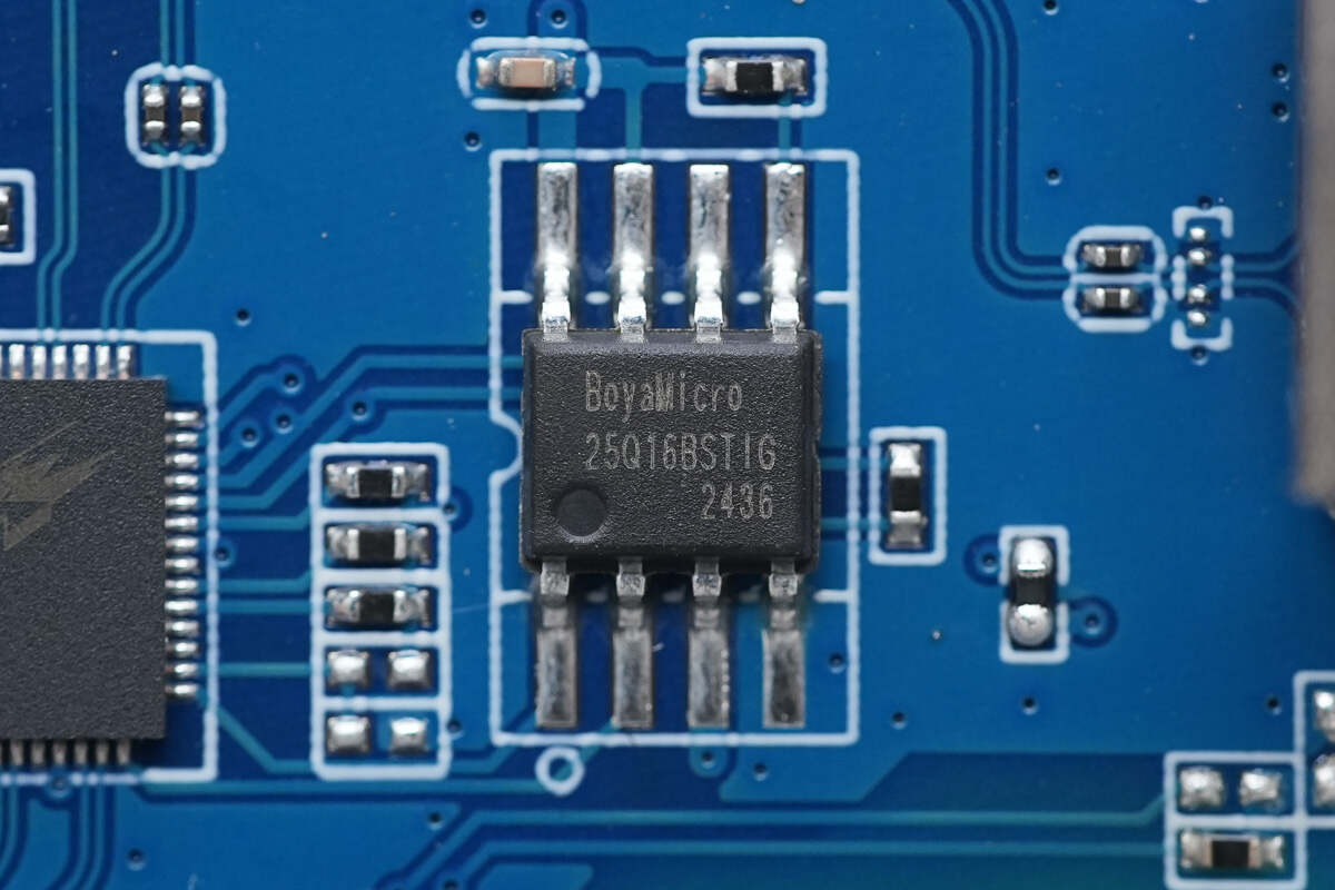
The memory is from BoyaMicro, model BY25Q16BSTIG, with a capacity of 2MB. It comes in an SOP8 package.
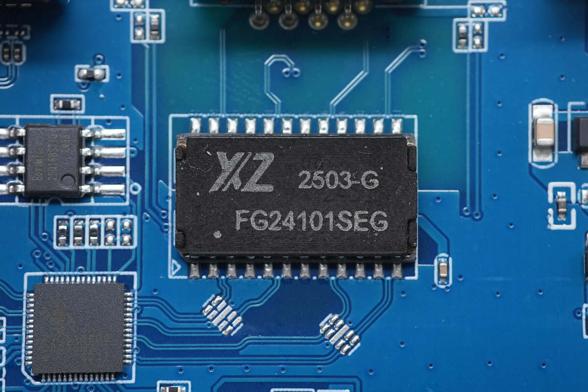
The network transformer is from YAN XING ZHI, model FG24101SEG, and is surface-mounted.
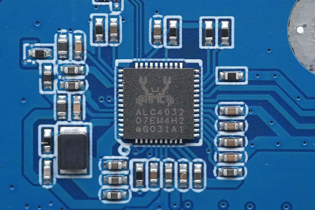
The audio chip is from REALTEK, model ALC4032. It is a low-power USB digital audio chip supporting 192kHz/24-bit sampling rate and comes in a QFN48 package.
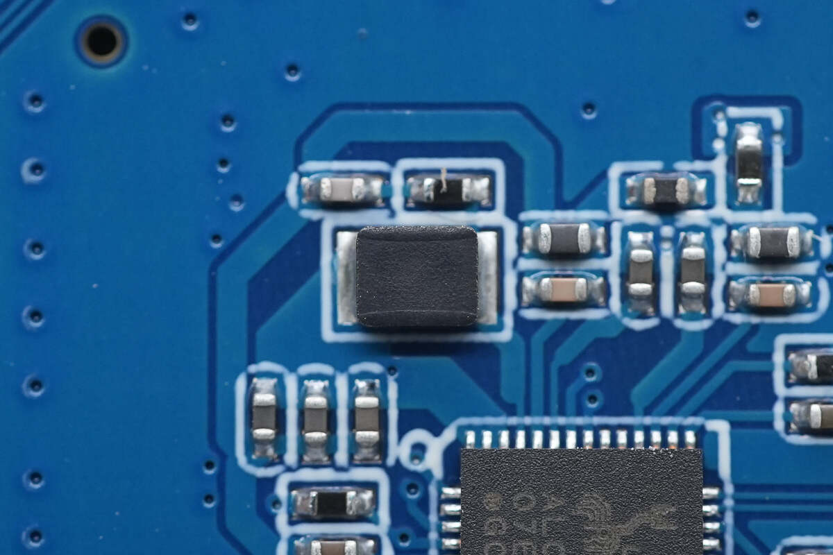
Close-up of external buck inductor.
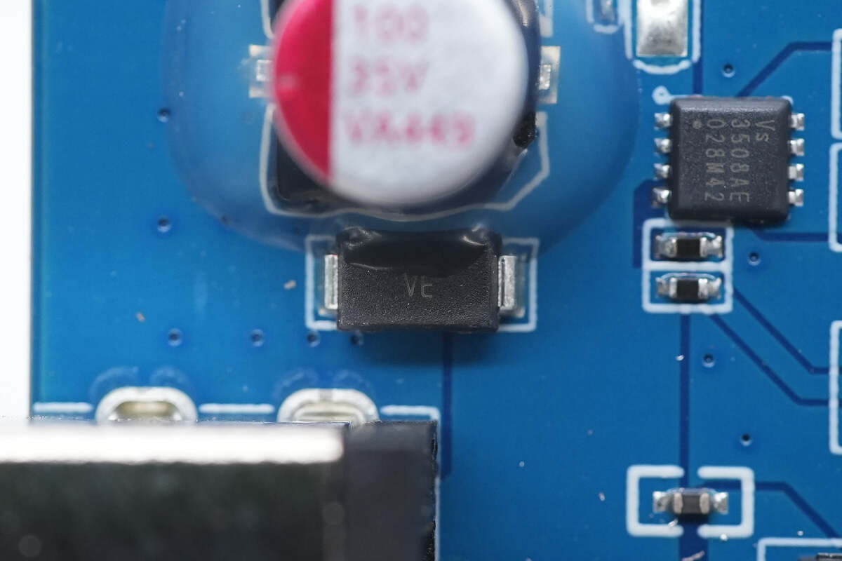
The input terminal is equipped with a TVS diode for overvoltage surge suppression.
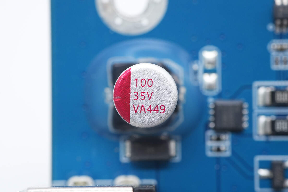
The input filter capacitor is rated at 100μF 35V.
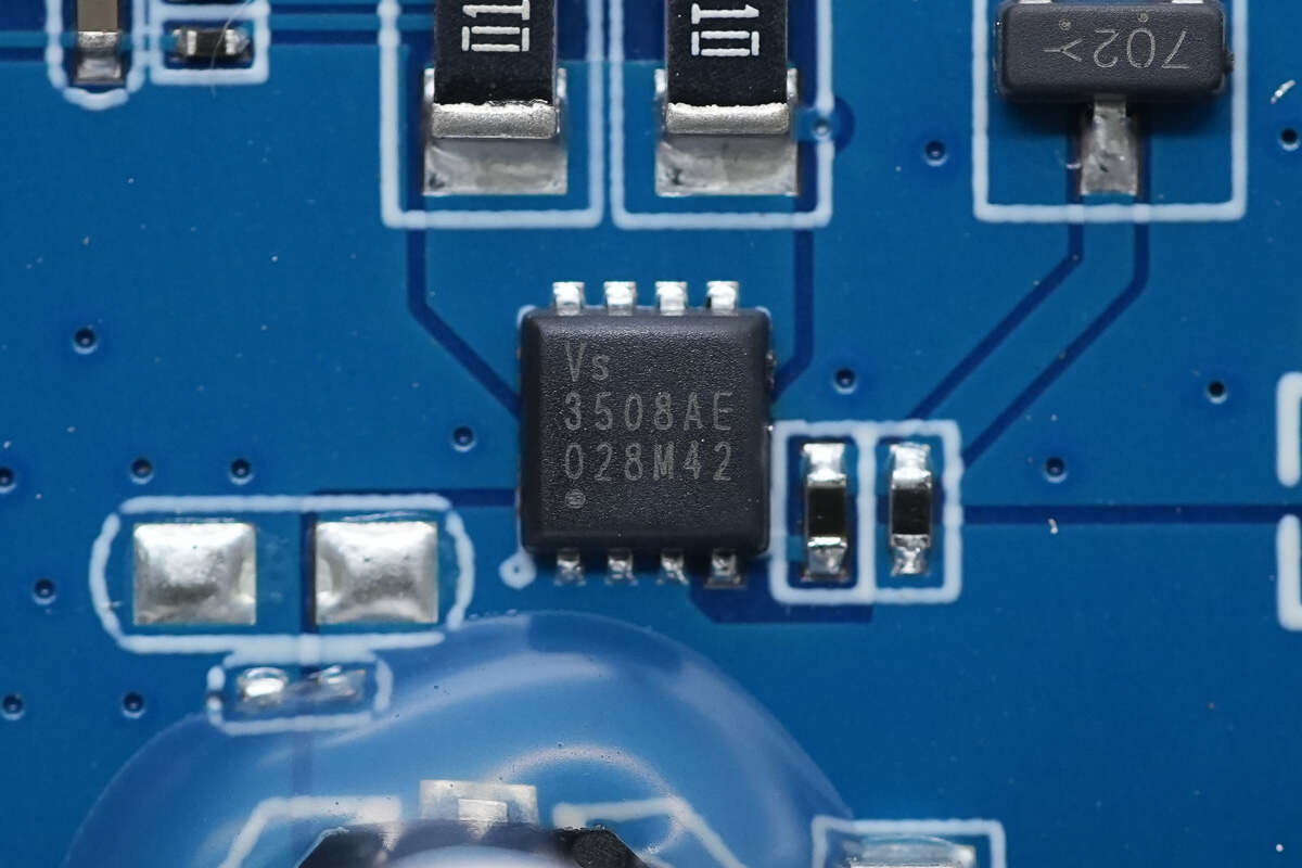
The MOSFET used for power control is from Vergiga, model VS3508AE. It is a PMOS with a voltage rating of -30V and an on-resistance of 8.5mΩ. It comes in a PDFN3333 package.
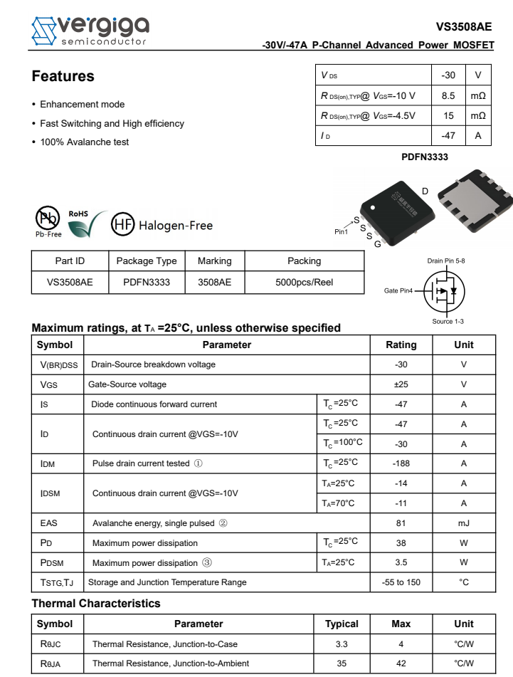
Here is information about Vergiga VS3508AE.
Close-up of current sensing resistors and filter capacitors.
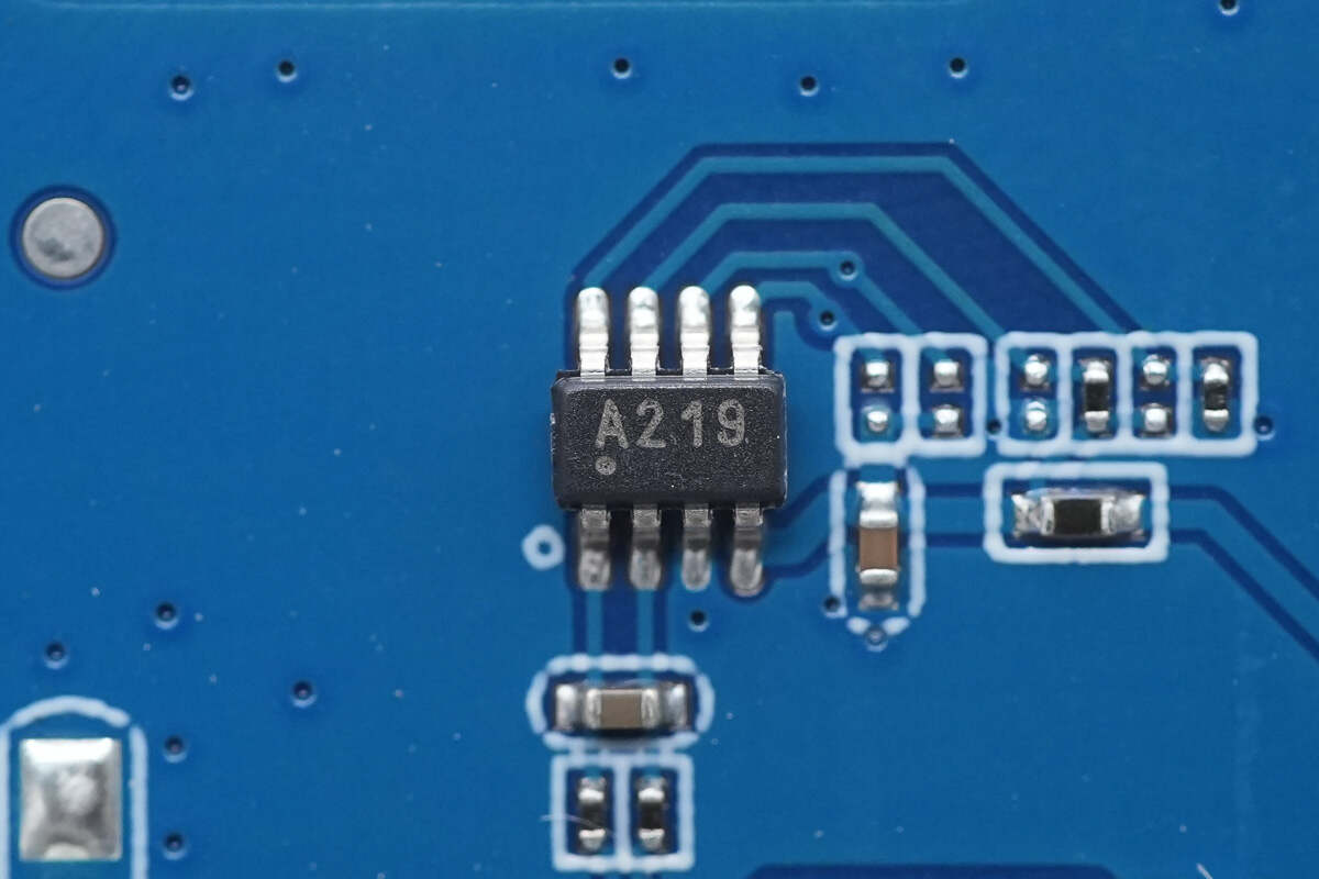
The current sensing chip is from TI, model INA219. It is a zero-drift bidirectional current and power monitoring chip with an I2C interface, supporting up to 26V. It features voltage and current detection channels and comes in a SOT23-8 package.
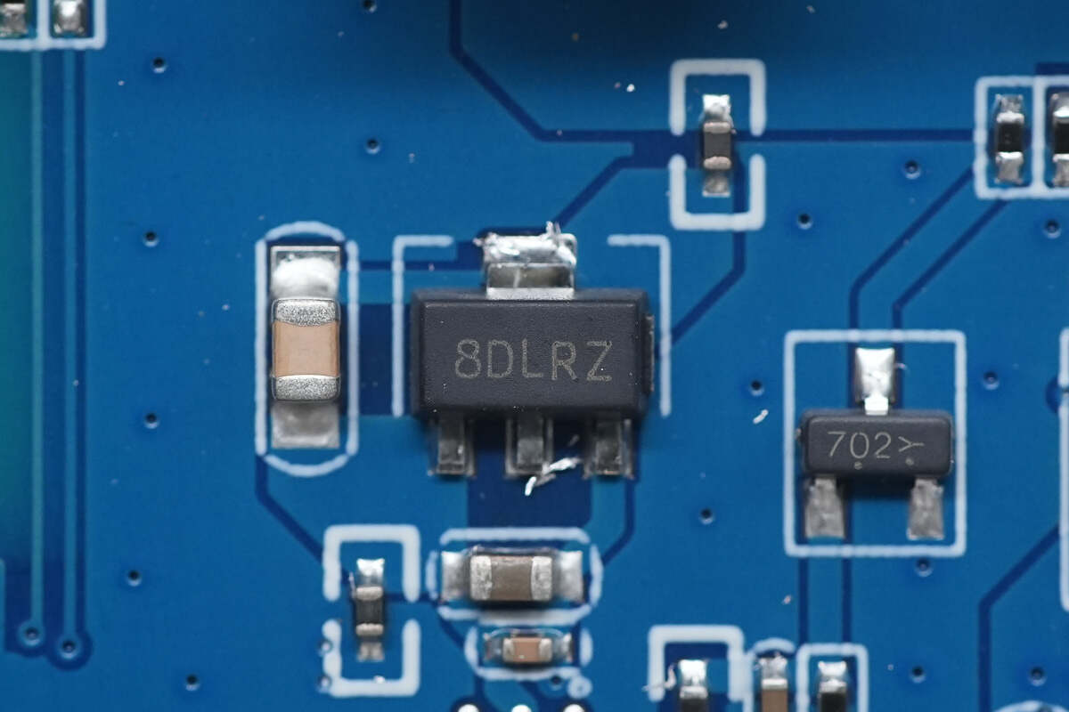
The voltage regulator chip is from LRC, marked with 8DL, model LR6375A33P. It supports an input voltage of up to 36V, outputs 3.3V at 250mA, and comes in a SOT-89-3 package.
Close-up of an unmarked chip.
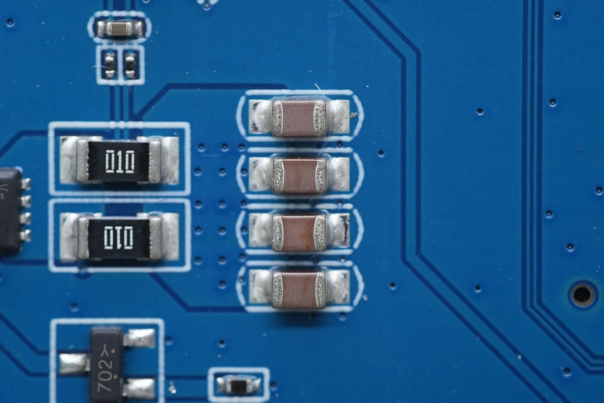
Close-up of synchronous buck converter chips and overcurrent protection chips.
All four synchronous buck converter chips use the ETA ETA3485S2F model.
The overcurrent protection chips are ETA ETA6280S2F.
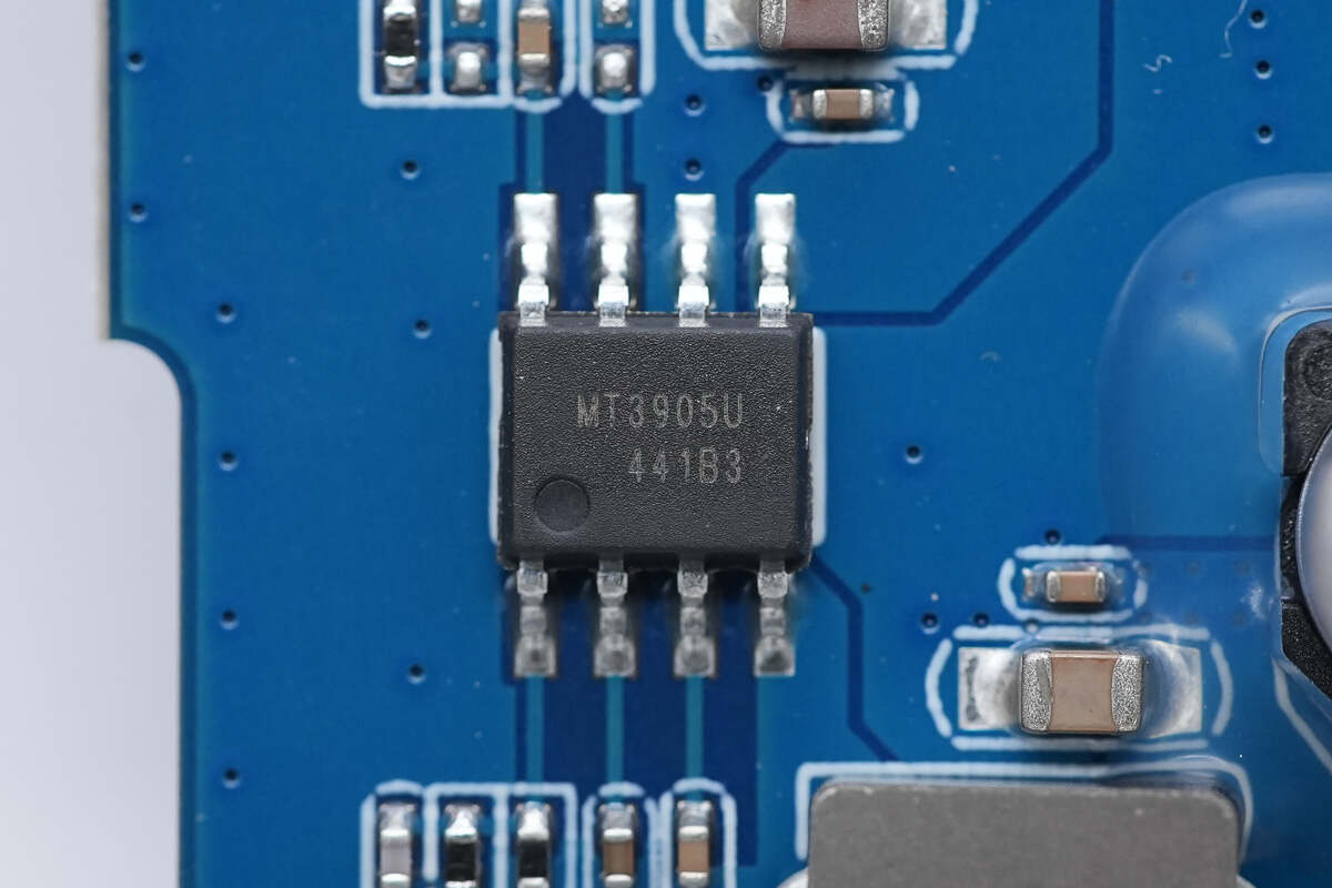
This synchronous buck converter chip is from M3TEK, model MT3905U. It supports a 30V input voltage, 4A continuous output current, and 5A peak output current. The chip integrates MOSFETs and comes in an SOP8-EP package.
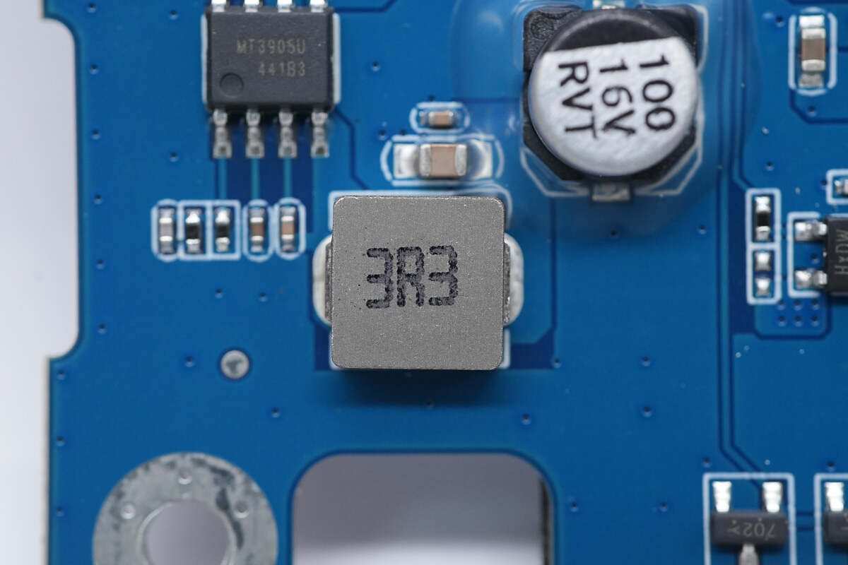
Close-up of 3.3μH alloy inductor.
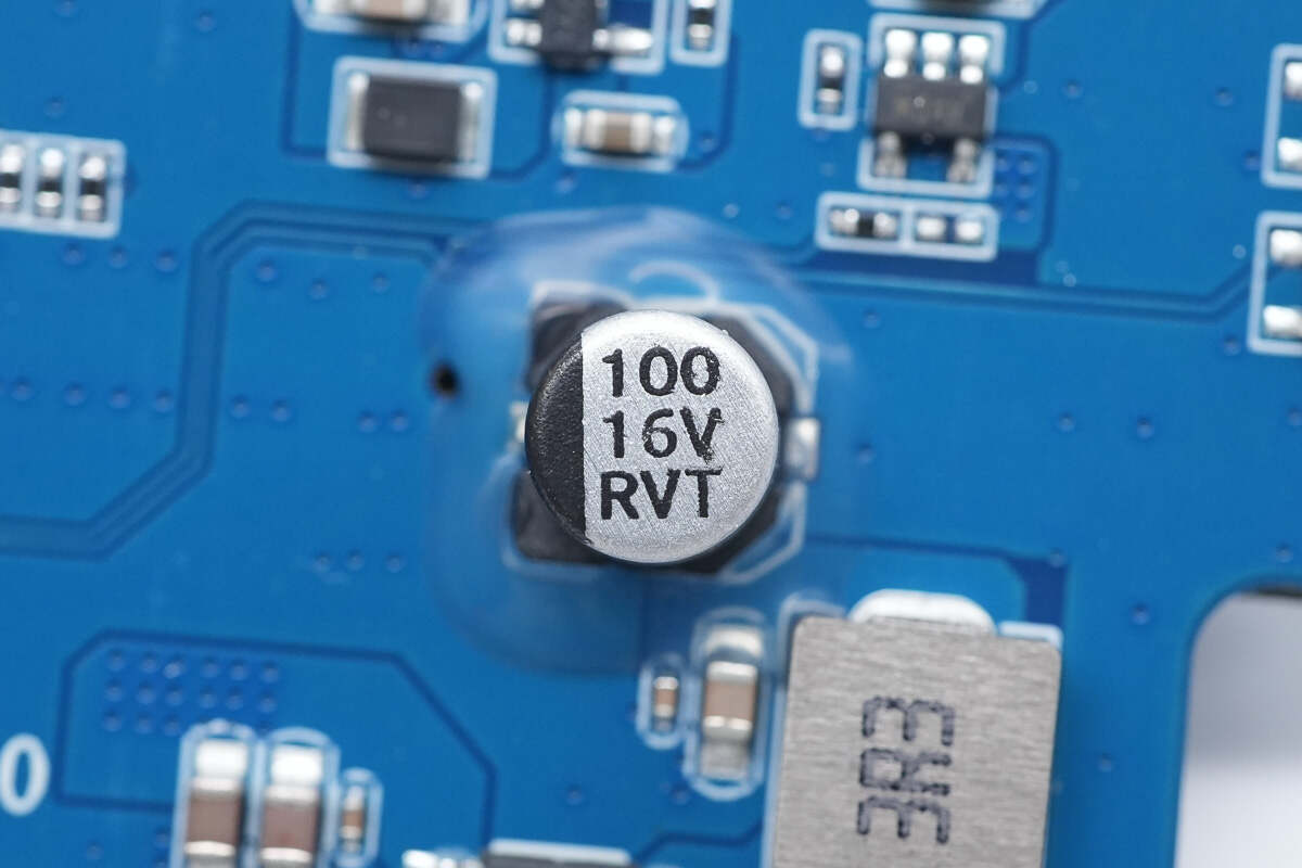
The output filter capacitor is rated at 100μF 16V.
The synchronous buck converter chip used is ETA ETA3485S2F.
Close-up of 2.2μH alloy inductor.
The synchronous buck converter chip used is Tollsemi TMI3410.
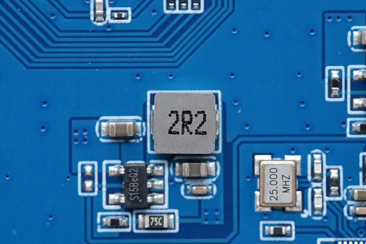
Close-up of 2.2μH alloy inductor.
The ETA ETA6280S2F is used for USB-A overcurrent protection.
The other overcurrent protection chip has the same model.
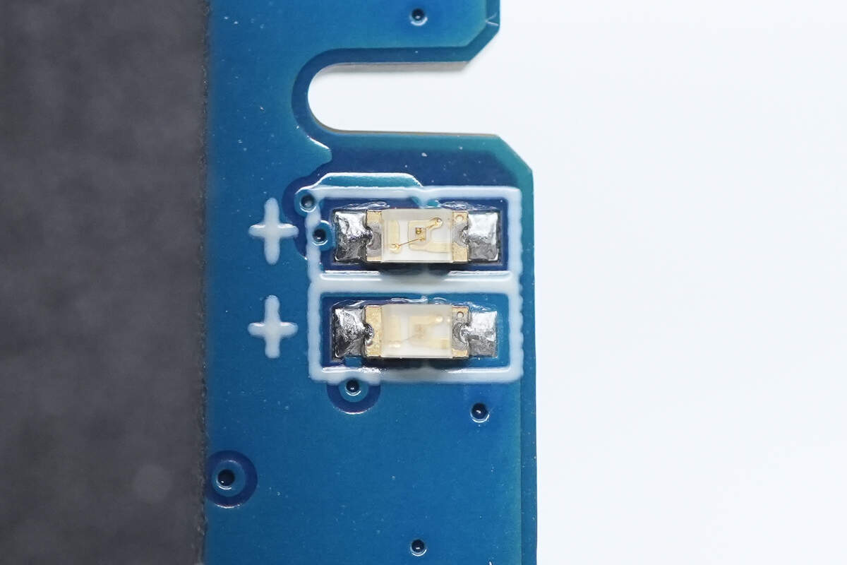
The SMD LED is used to indicate the dock’s operating status.
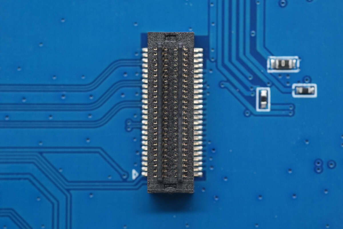
Close-up of the connector used to connect two PCBs.
The TF card slot uses surface-mount soldering.
The SD card slot also uses surface-mount soldering.
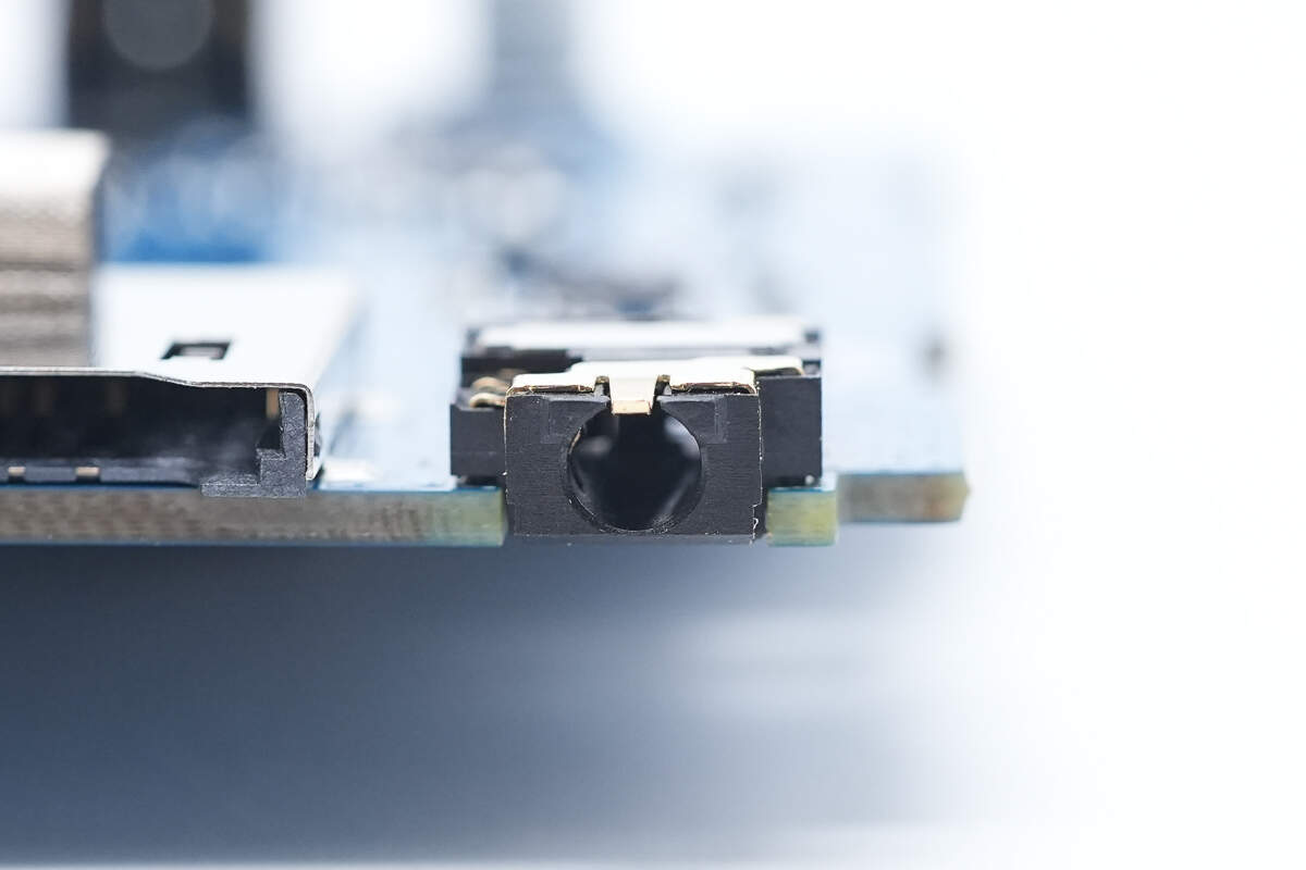
The 3.5mm audio jack uses flush-mount soldering.
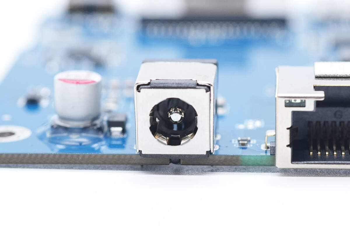
The power socket is secured by through-hole soldering.
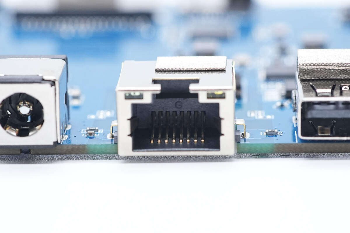
The Ethernet port uses flush-mount soldering to reduce thickness and is equipped with an indicator light.
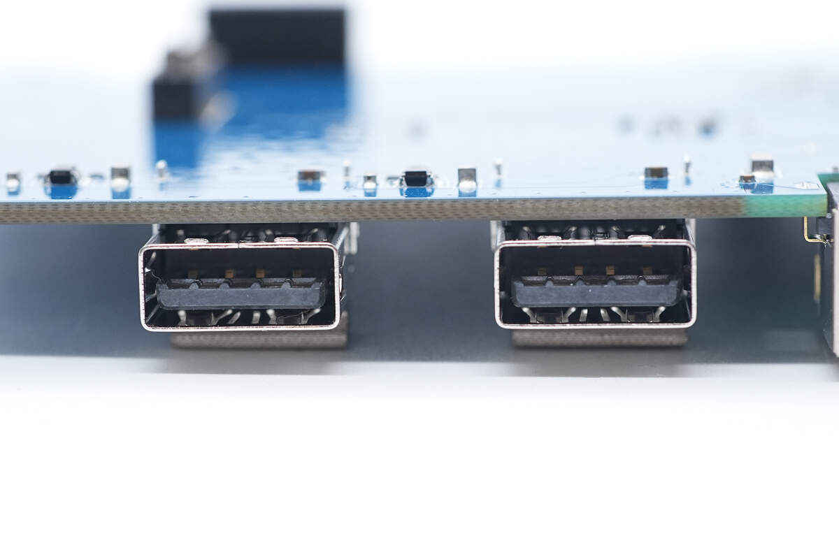
The USB-A sockets are secured by through-hole soldering.
Well, those are all components of the UGREEN Revodok Max Thunderbolt 5 Docking Station.
Summary of ChargerLAB
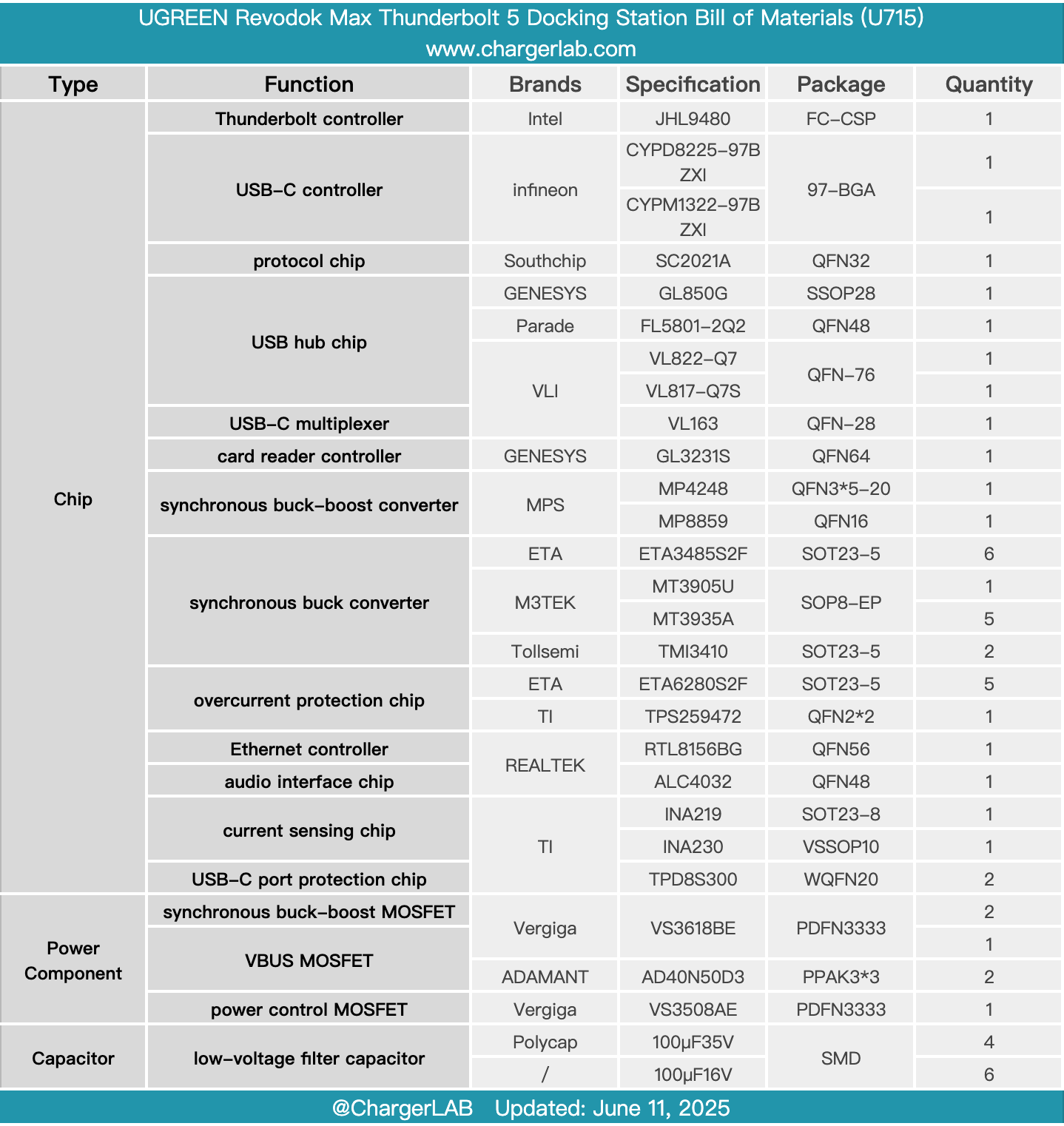
Here is the component list of the UGREEN Revodok Max Thunderbolt 5 Docking Station for your convenience.
It features an aluminum alloy casing and is powered by an external power supply. The front side includes USB-C and USB-A ports, as well as SD and TF card slots. The rear side is equipped with Thunderbolt 5 ports, an Ethernet port, and USB-A ports.
After taking it apart, we found that the PCBA module is equipped with shielding covers and heat sinks, fixed by standoffs. It consists of two PCBs connected by connectors. It uses the Intel JHL9480 Thunderbolt 5 controller paired with an Infineon USB-C controller to enable multiple Thunderbolt 5 port expansions.
USB-A and USB-C ports are expanded using VIA Labs hub controllers. MPS MP4248 and MP8859 synchronous buck-boost converters are used for voltage conversion. Both the Ethernet controller chips and audio chips come from REALTEK. Thermal pads are applied to heat-generating chips, and heat is dissipated through the shielding cover, ensuring stable and reliable operation.
Related Articles:
1. Teardown of Xiaomi 22.5W 5000mAh Magnetic Wireless Power Bank (WPB0507S)
2. Teardown of HUAWEI 3000W R4850G1 Power Supply Unit
3. Teardown of CUKTECH 10 GaN Charger Ultra (AD1204U)