Introduction
UGREEN's new 45W USB-C GaN charger has arrived at ChargerLAB. It pairs a premium metallic and skin-friendly finish with a sleek, rounded design that feels great in the hand. The highlight is a uniquely positioned 45° angled display on the front, ensuring clear visibility regardless of whether it is plugged into a wall outlet or a desktop strip.
The screen provides a comprehensive look at your power metrics—total output, current, voltage, charging protocols, and temperature—all in real-time. It also adds a layer of fun, letting users switch between various dynamic emoji animations for a more personalized experience.
Compatibility is another strong point, as the charger supports UFCS, QC, and PD 3.2/AVS protocols, ensuring it can fast-charge most smartphones, tablets, and lightweight laptops.
While ChargerLAB has previously torn down the Anker Nano 45W GaN charger, the two devices represent distinct approaches to product design despite their identical 45W power output.
Now, let's dive into the UGREEN 45W GaN charger with a full teardown to reveal what’s inside.
Product Appearance
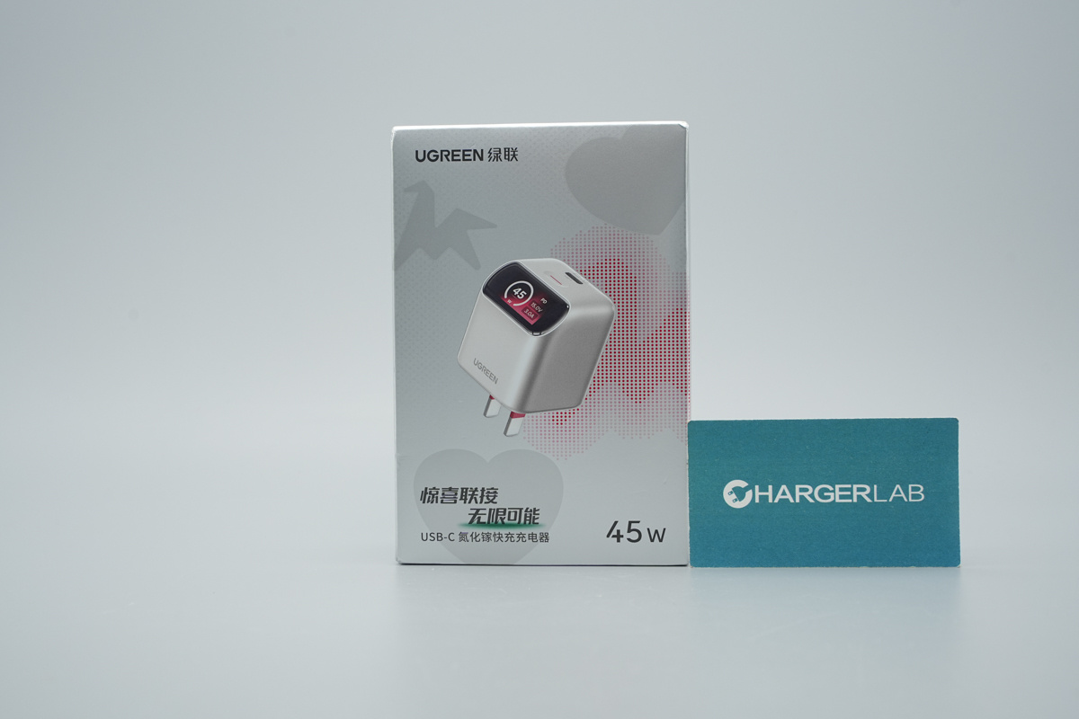
The packaging box's silver-gray front showcases the UGREEN logo, a product rendering of the charger, and the"45W" branding accompanied by the slogan "Surprising Connection, Infinite Possibilities."
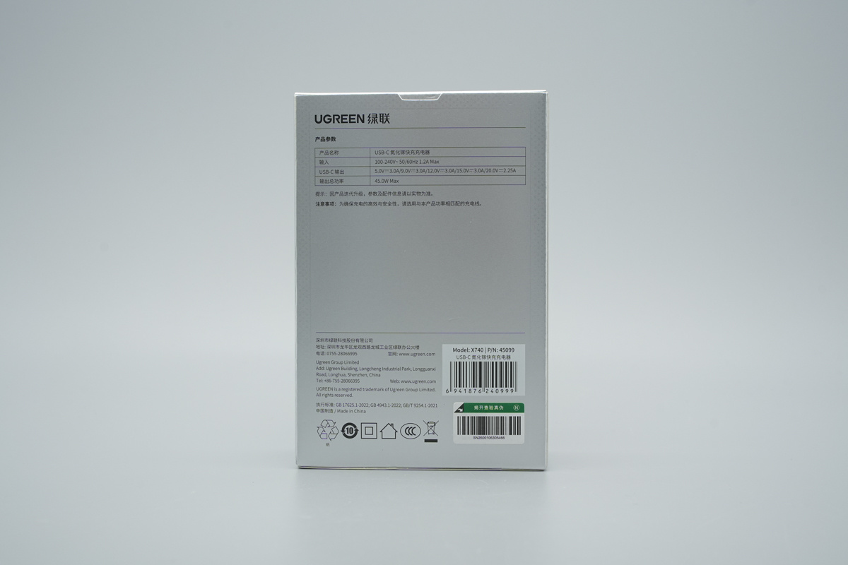
The back of the package features comprehensive specs, manufacturer details, and an anti-counterfeiting label. Technical specs will be detailed in the upcoming physical teardown section.
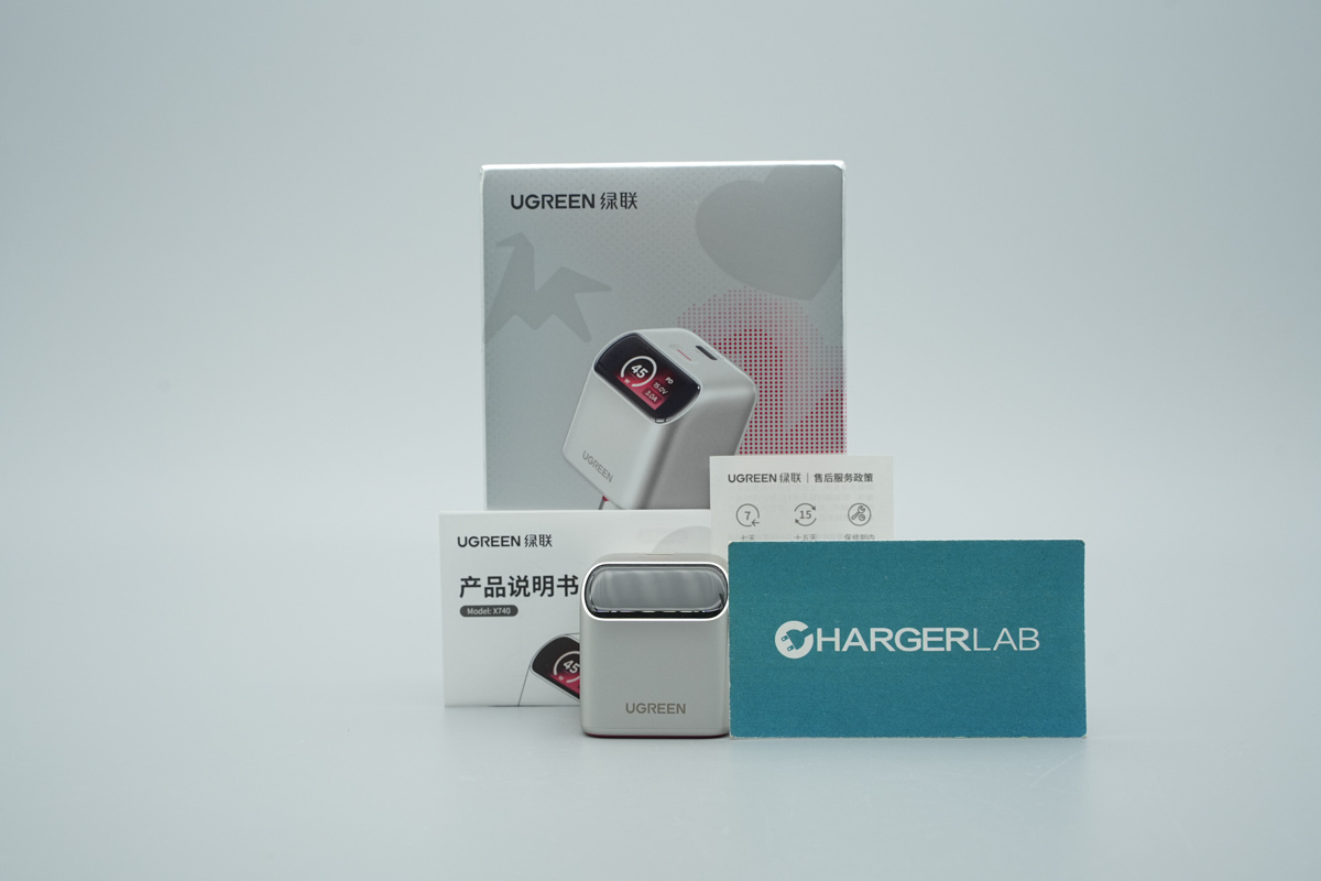
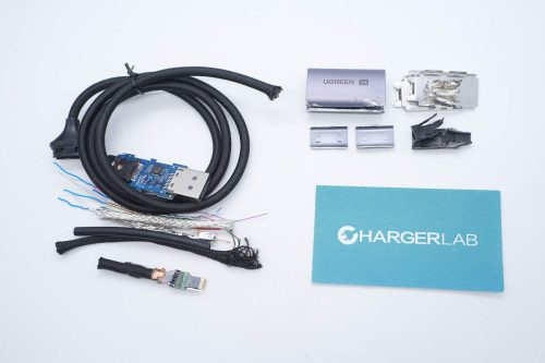
Inside the box, you will find the charger, the instruction manual, and the warranty card.
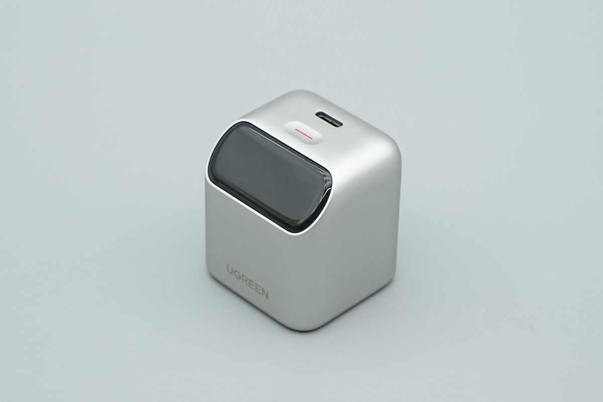
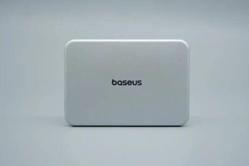
The charger sports a silver-gray shell with smooth, rounded edges and a distinct black high-gloss display area on the front for a highly recognizable look.
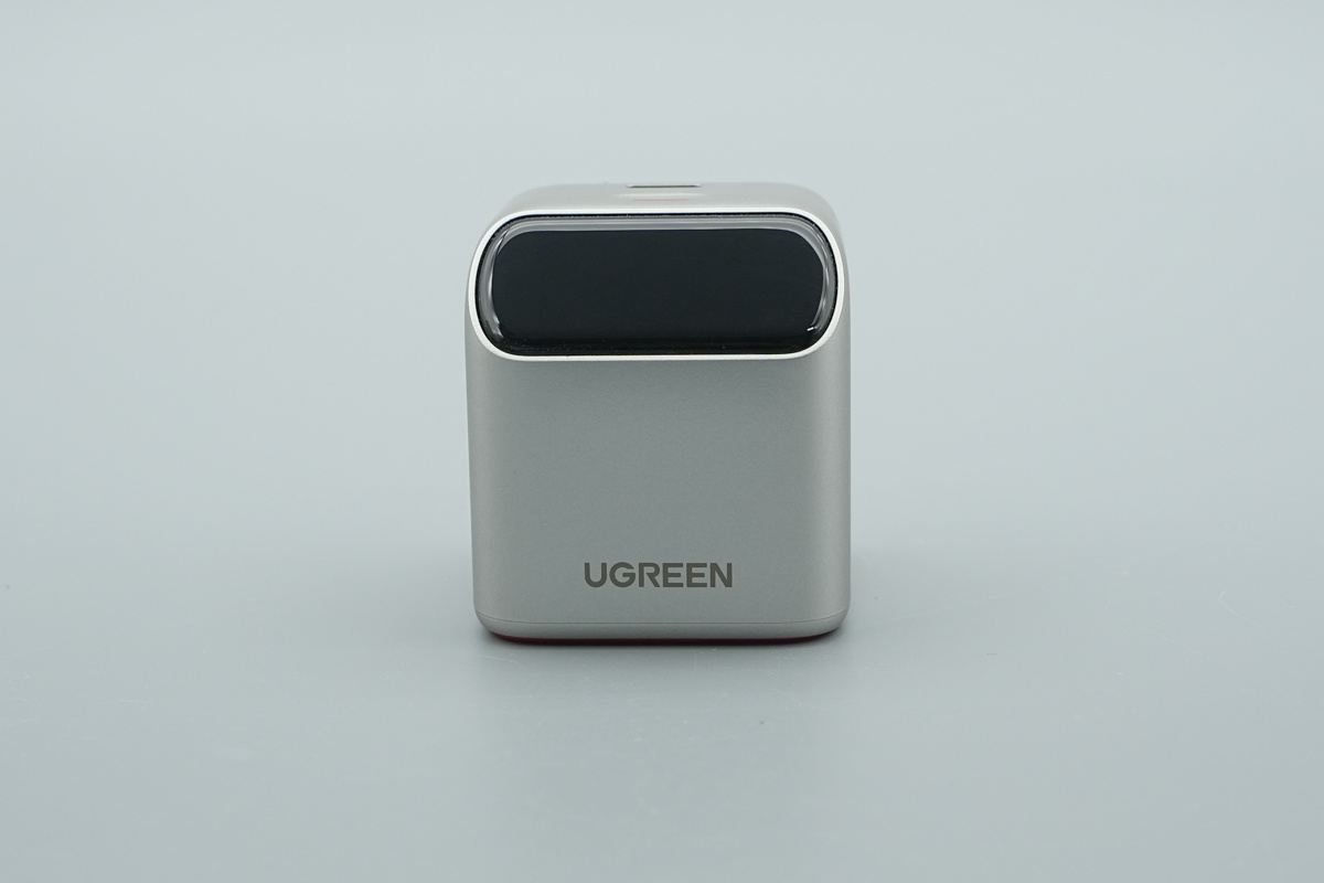
The UGREEN logo is located beneath the screen.
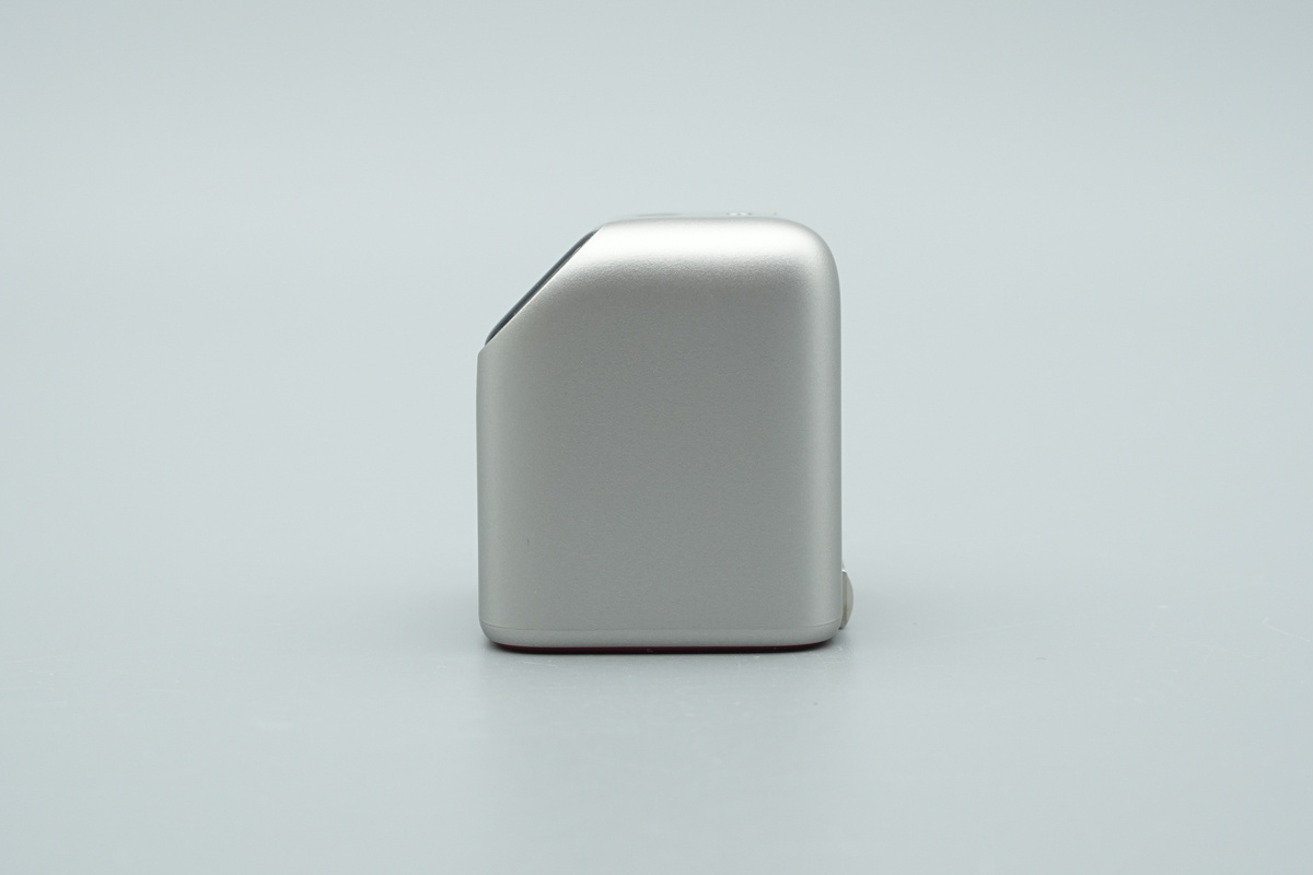
The side profile reveals a natural tilt to the display panel, ensuring that users can easily read screen info from a comfortable angle, whether it's plugged into a wall or a desk power strip.
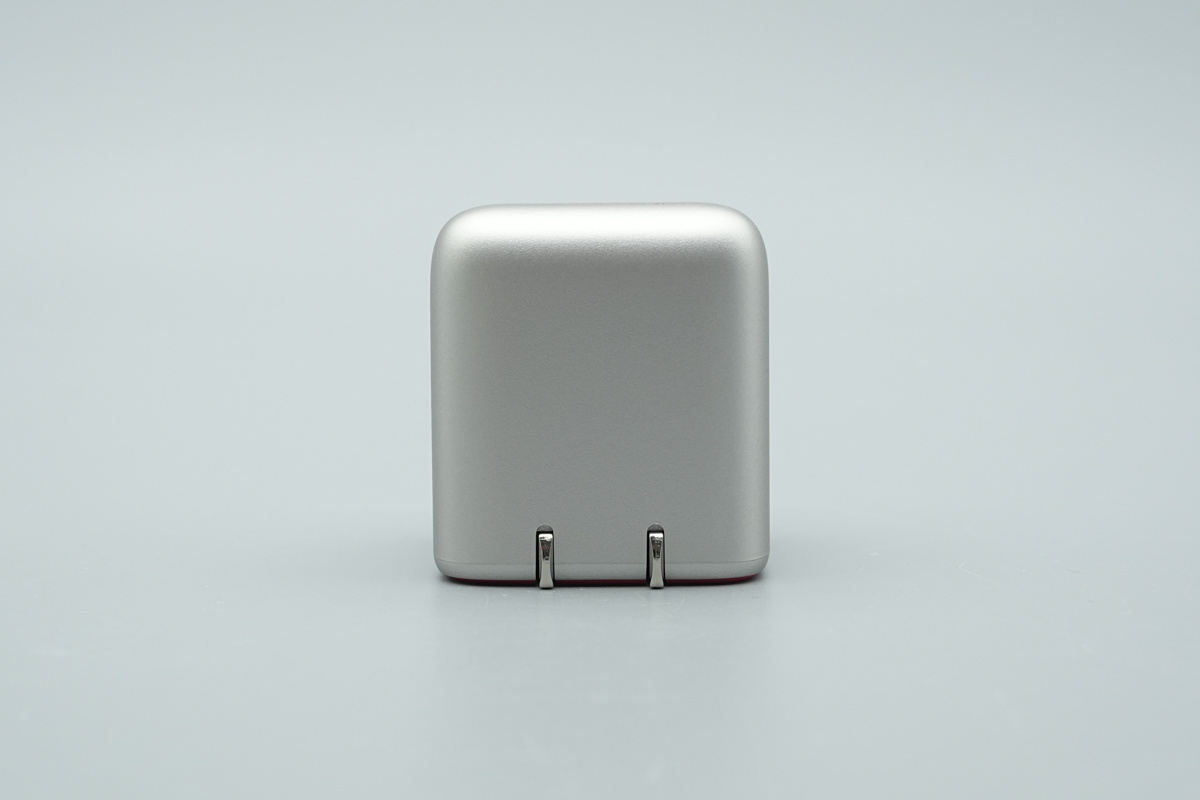
The back of the charger features a minimalist design, with the foldable plug clearly visible at the bottom.
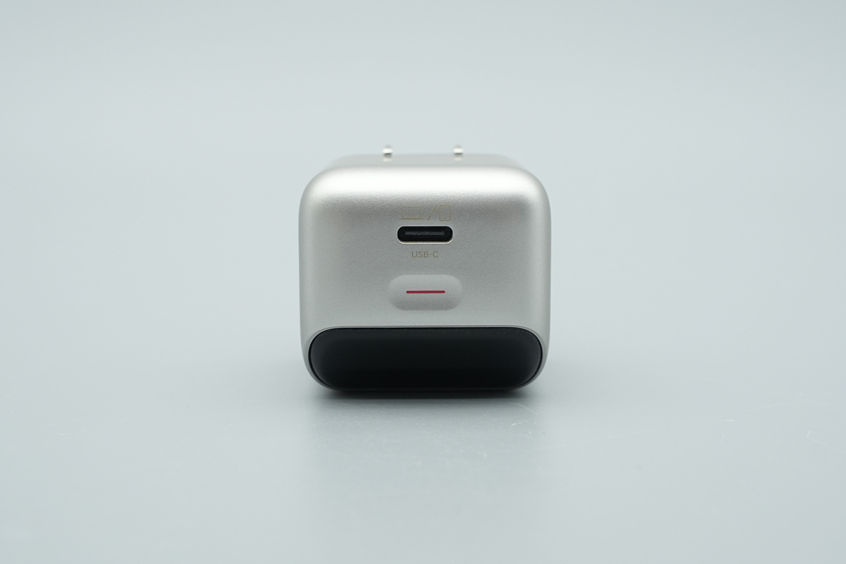
The top panel features a single USB-C output port, accented by laptop and smartphone icons above and a red touch-sensitive control zone beneath.
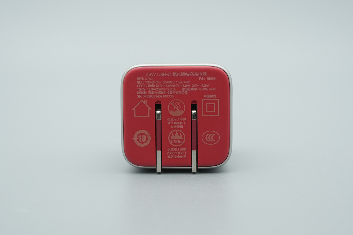
The base features a striking red design and includes a foldable, new Chinese standard plug, making it easy to pack for travel.
Product specs are listed below:
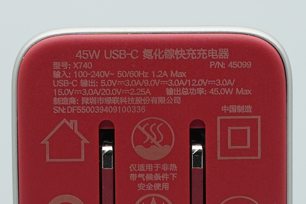
Model: X740
Input: 100-240V~ 50/60Hz 1.2A Max
USB-C Output: 5V3A, 9V3A, 12V3A, 15V3A, 20V2.25A (45.0W Max total)
Manufacturer: Ugreen Group Limited
Origin: Made in China
Certification: Chinese 3C certified.
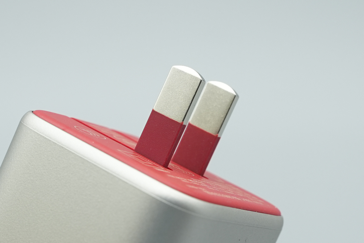
The foldable, new Chinese standard plug is well-built and completely free of burrs.
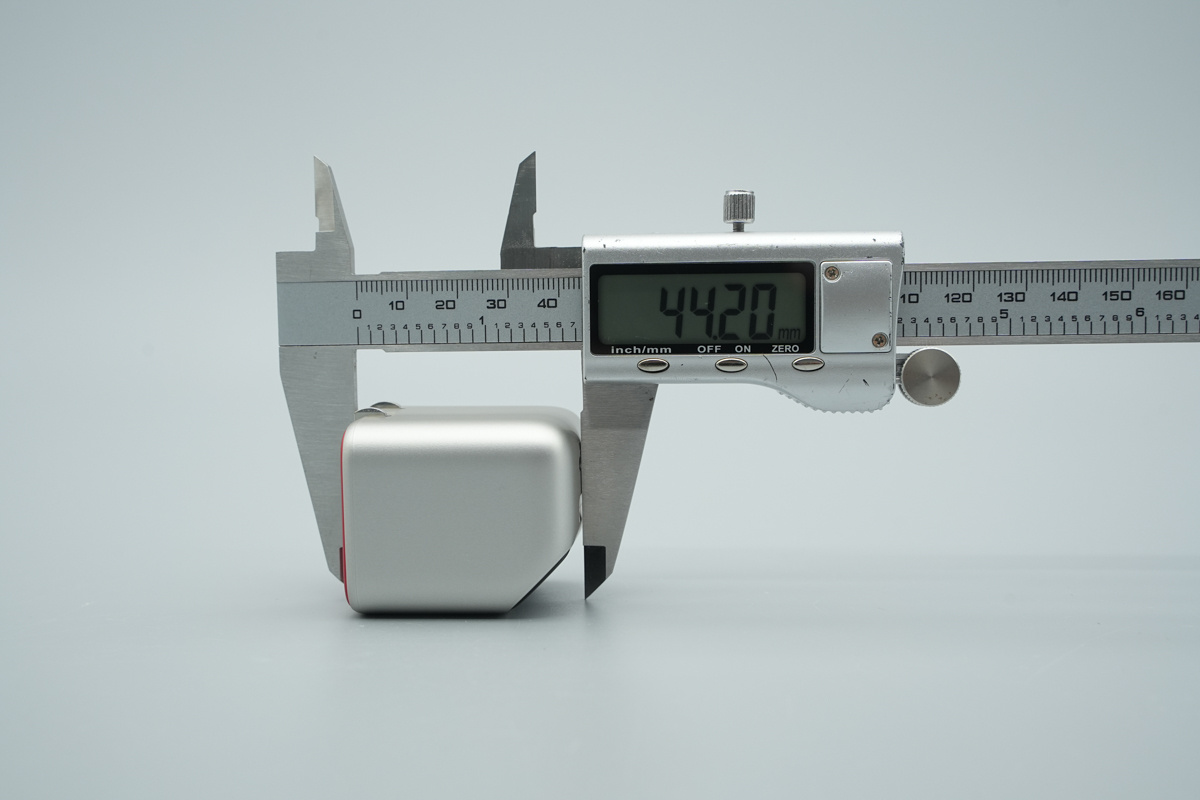
The height of the charger is about 44.20mm (1.740 inches).
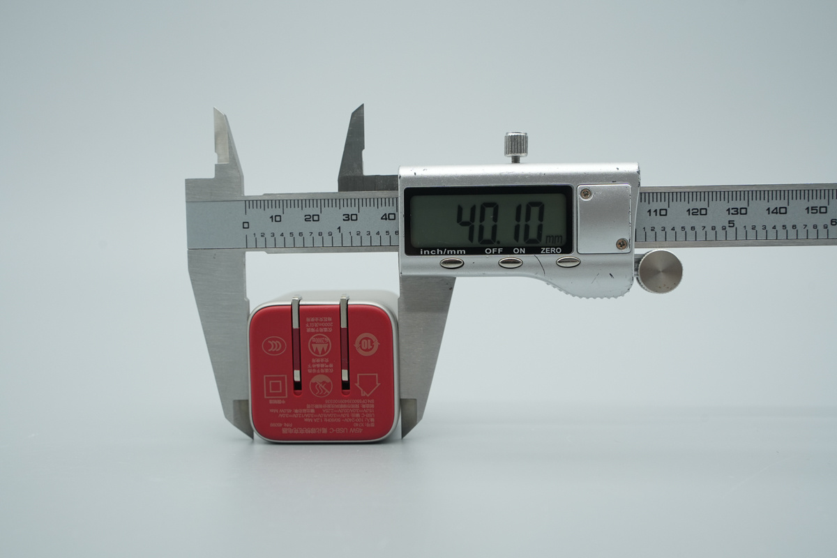
The length of the charger is about 40.10mm (1.579 inches).
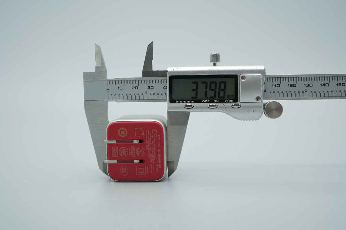
The width of the charger is about 37.98mm (1.495 inches).
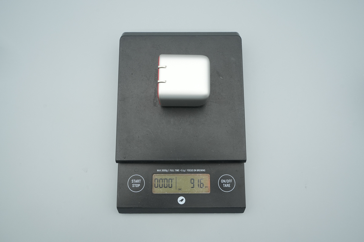
The weight is about 91.6g (3.23 oz).
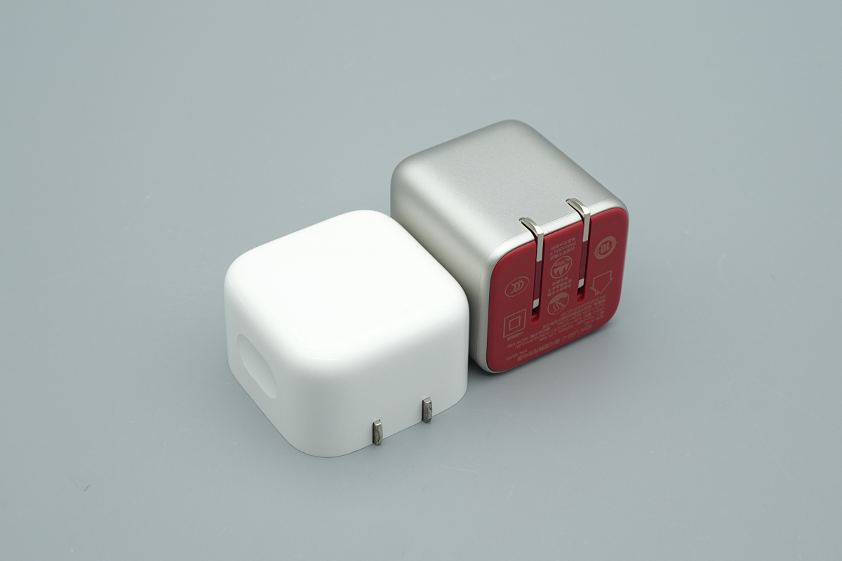
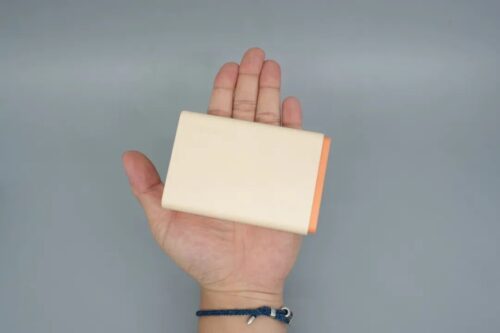
Put it with Apple’s 40W dynamic charger, as illustrated in the image.
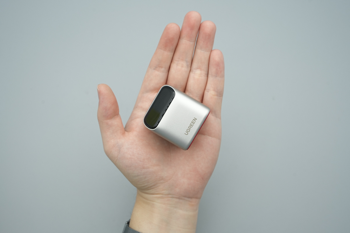
That's how big it is in the hand.
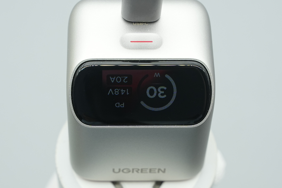
The display shows live charging data, including power, protocols, voltage, and current. You can easily toggle between device info, power status, temperature, and settings by clicking the button.
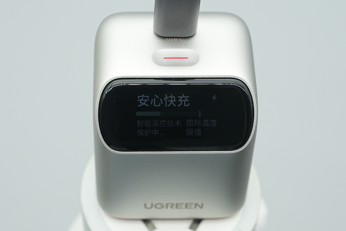
A click cycles to the safe charging and temperature limit display, confirming that intelligent thermal management and international temperature safeguards are currently in operation.
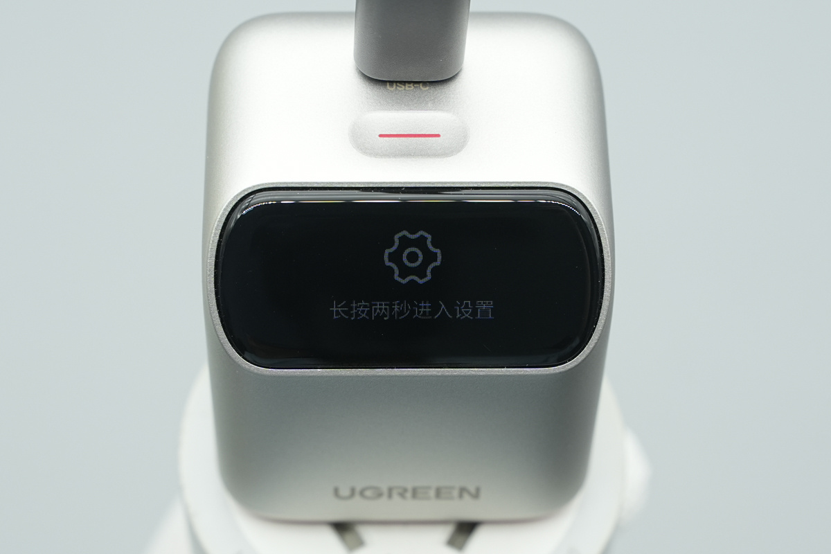
Navigate to the settings interface and hold for two seconds to enter the menu.
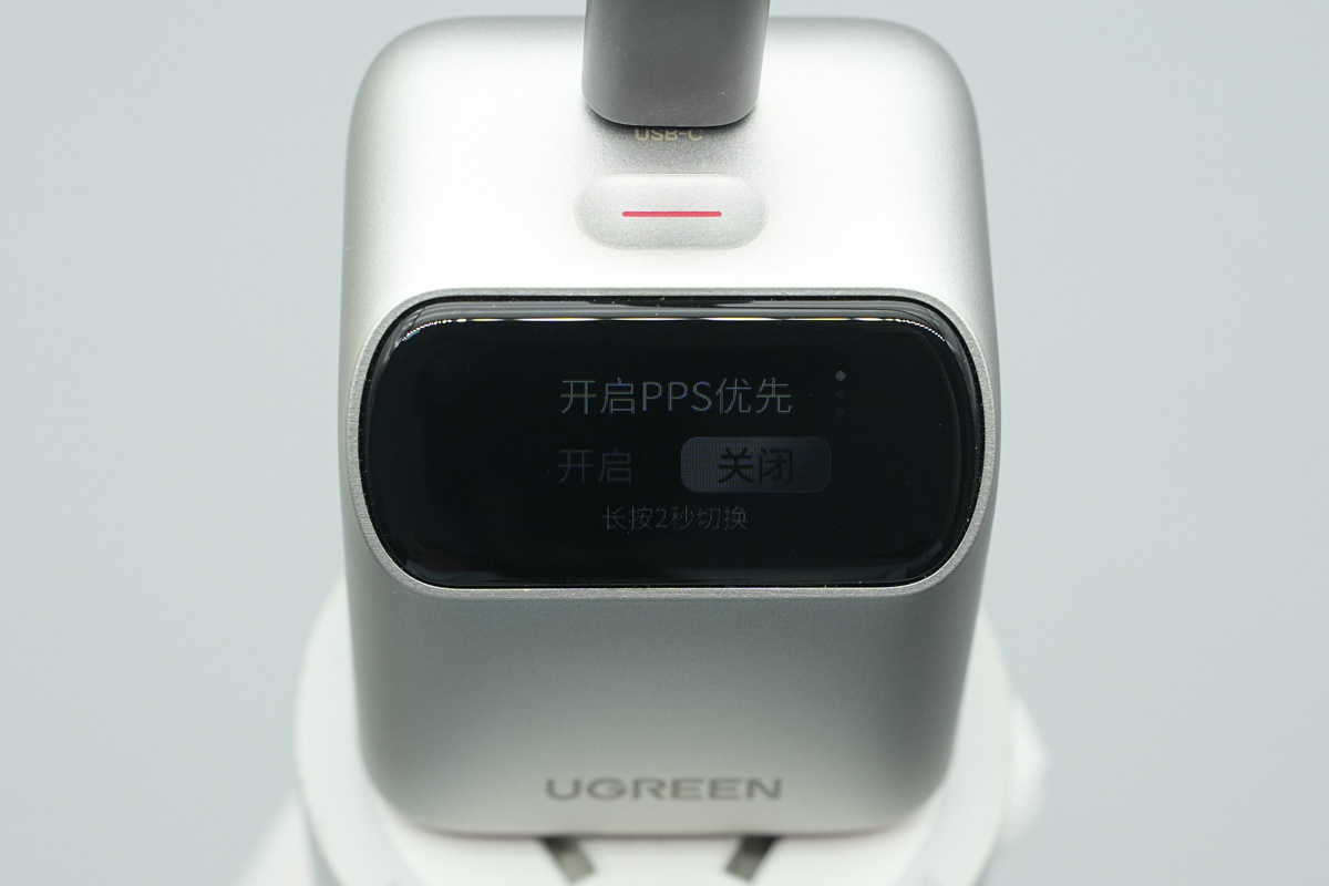
Within the settings menu, a long press of two seconds allows you to enable or disable the PPS priority feature.
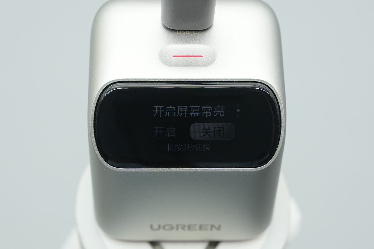
Users can similarly toggle the "Always-on Display" feature.
Long press for three seconds to flip the screen orientation, while holding the button to cycle through display rotations.
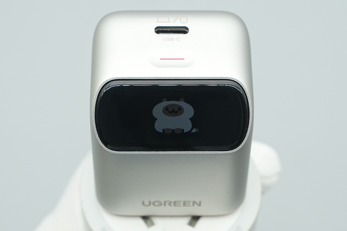
Cycles through four preset animations on the screen when left in an idle state.
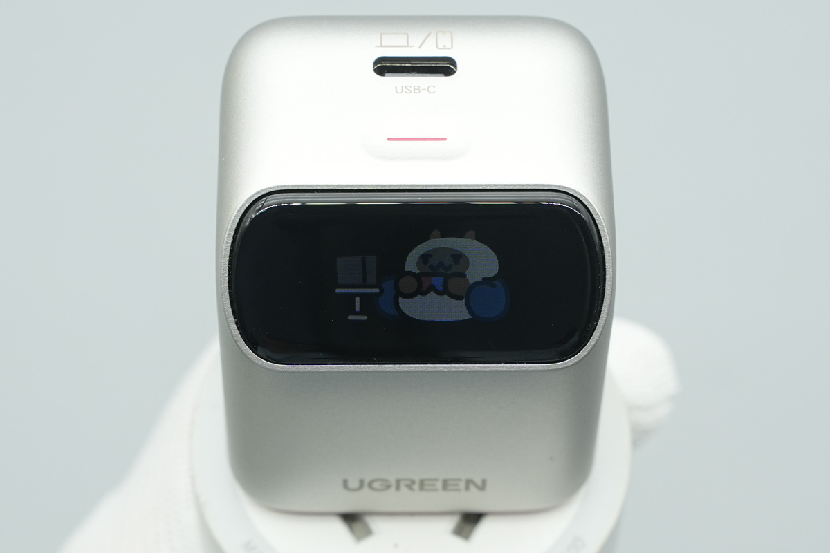
Demonstrating another preset animation state.
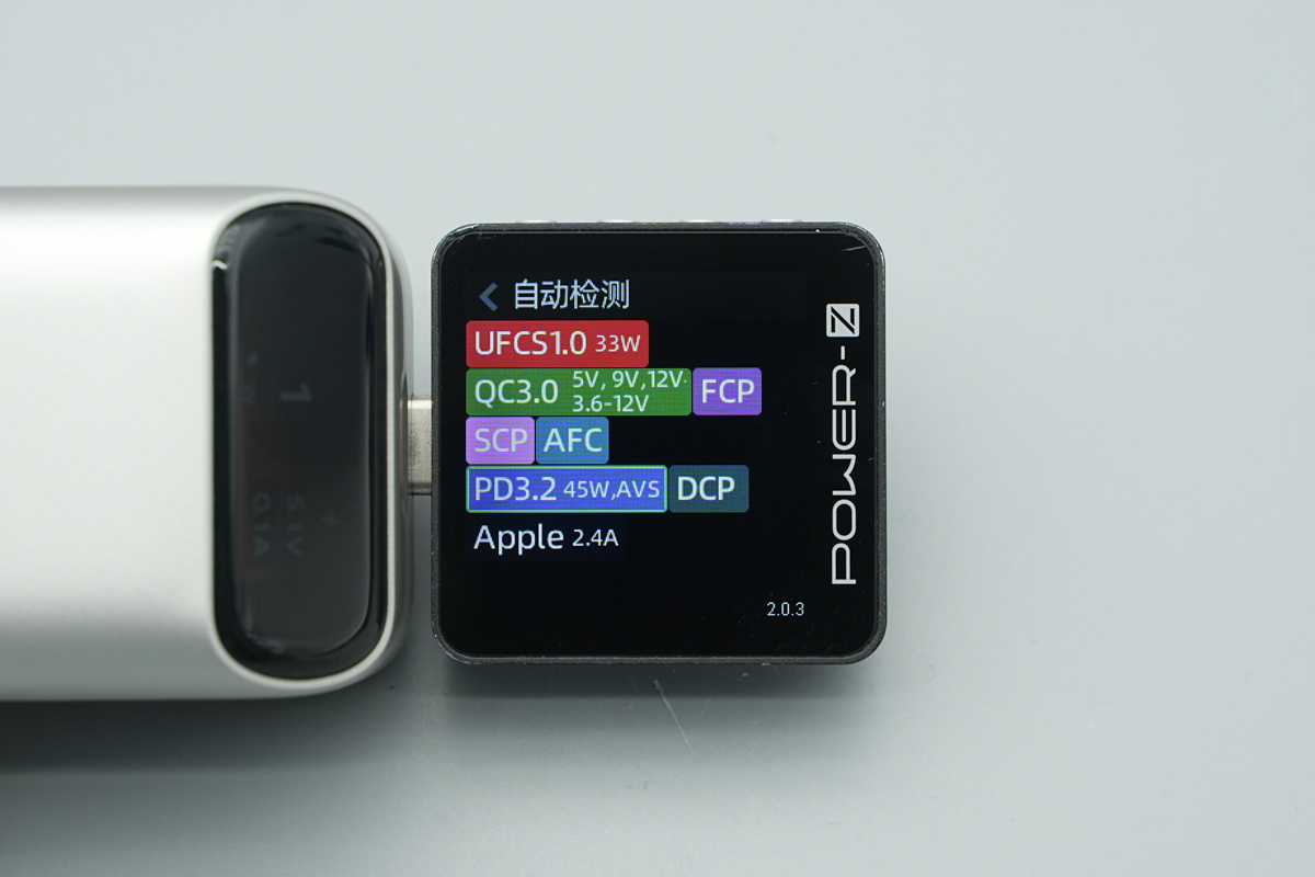
ChargerLAB POWER-Z KM003C shows that the USB-C port supports 1.0, QC3.0, FCP, SCP, AFC, PD3.2/AVS, DCP and Apple 2.4A.
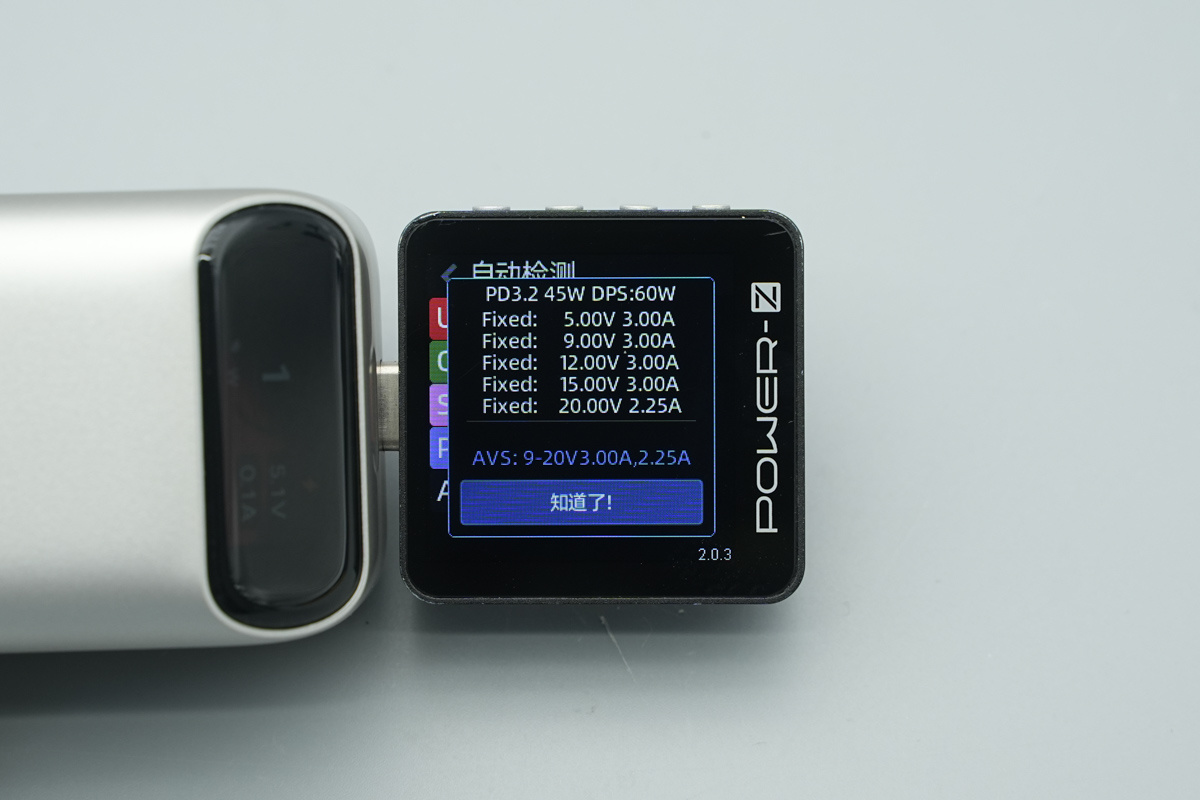
And it also supports four fixed PDOs of 5V3A, 9V3A, 12V3A, 15V3A and 20V2.25A, and features AVS subset: 9-20V 3A, 2.25A.
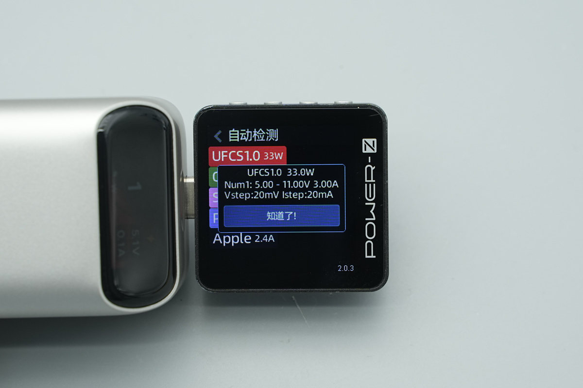
And it shows that the UFCS supports a voltage range of 5–11V at 3A.
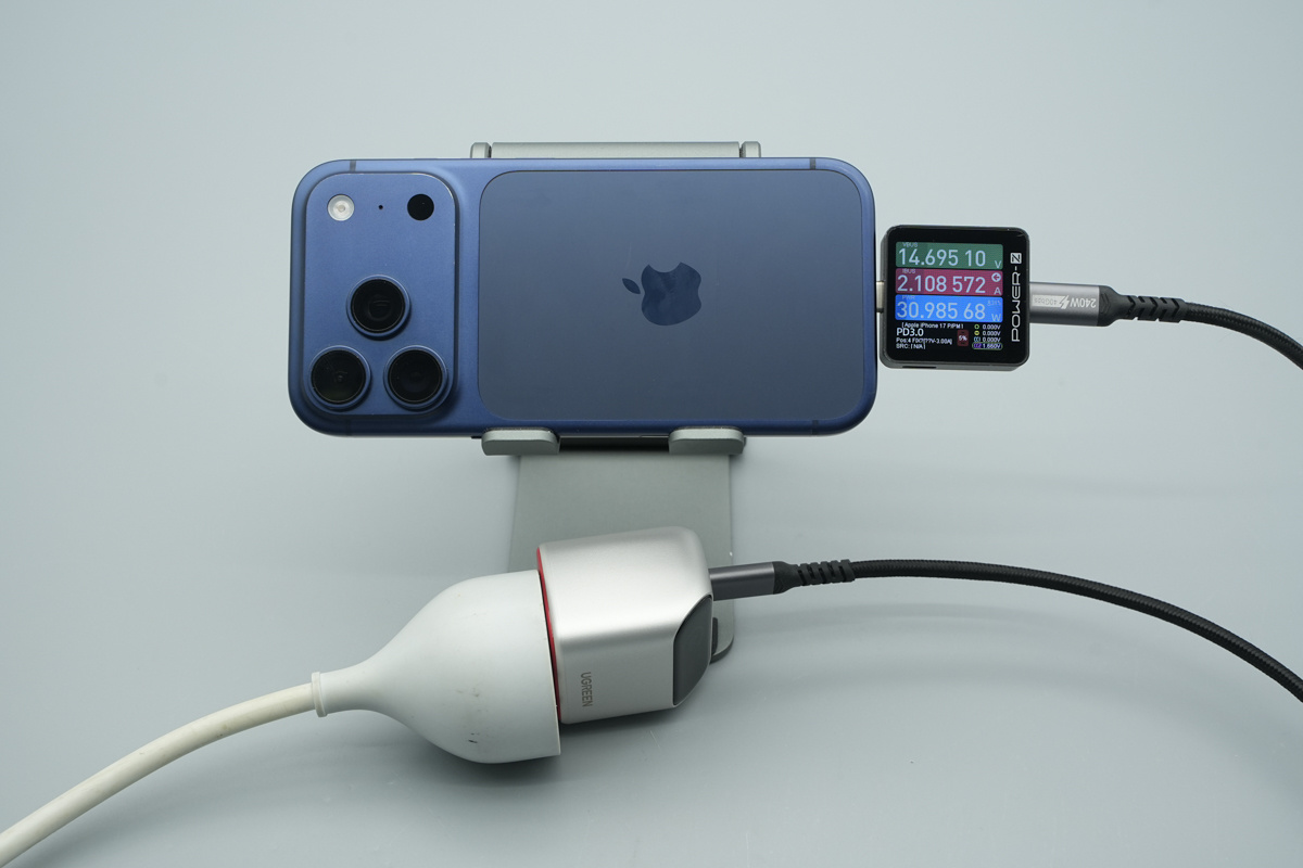
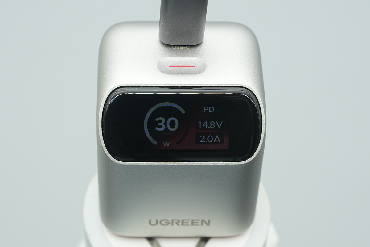
When charging the iPhone 17 Pro, the charging power can reach up to 30W.
After a quick look at the design and protocol compatibility, let's moving on to the full product teardown.
Teardown
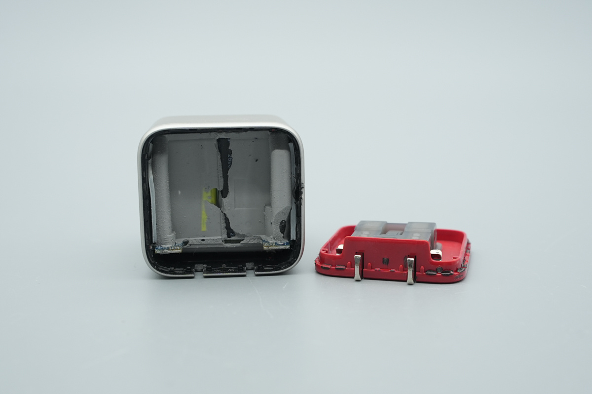
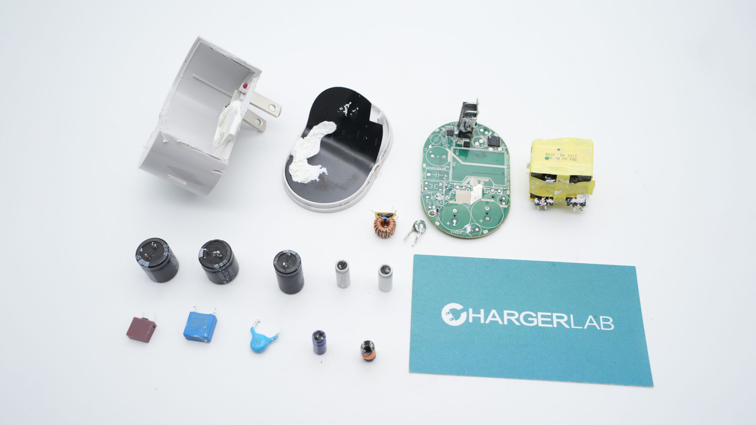
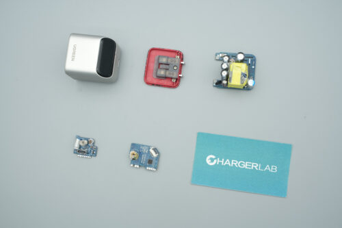
Pry the red ultrasonic-welded bottom cover along the seam, the PCBA is fully encapsulated in gray thermal potting compound.
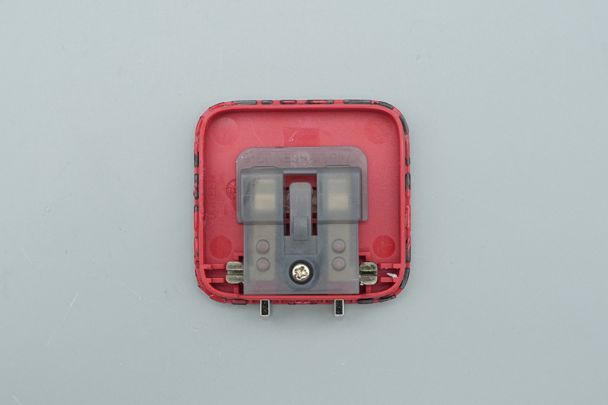
Foldable plug assembly located inside the red bottom cover, connecting to the PCBA via two metal contacts to supply power.
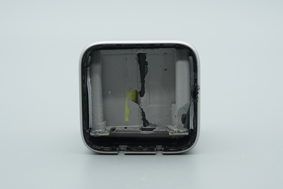
Interior filled with gray potting compound, which ensures effective thermal management and improves drop resistance.
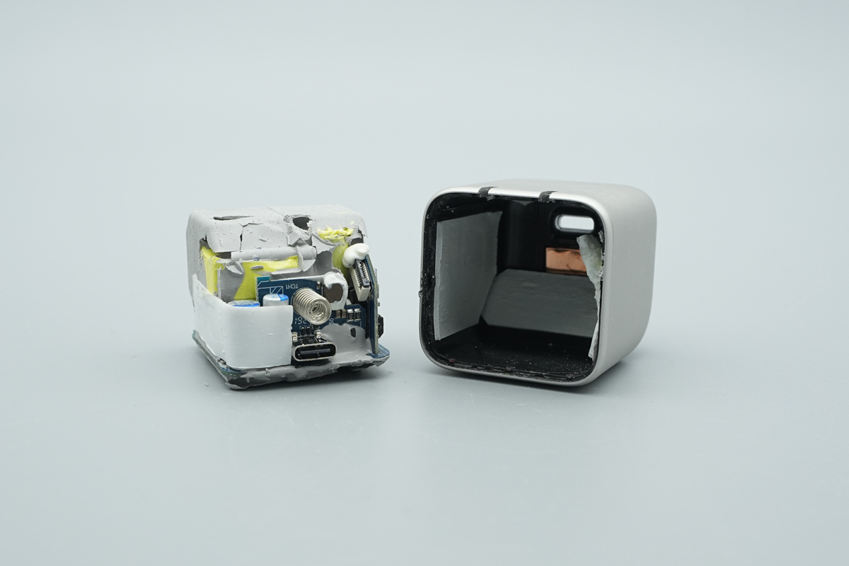
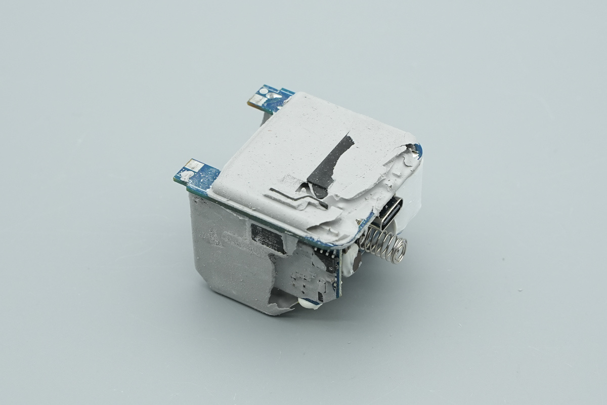
The entire PCBA module is pulled out from the silver housing.
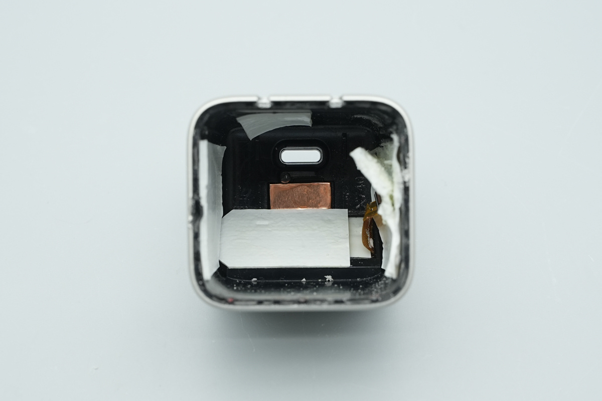
Interior sidewalls are fitted with thermal sheets and a copper-foil-covered touch-sensing zone.
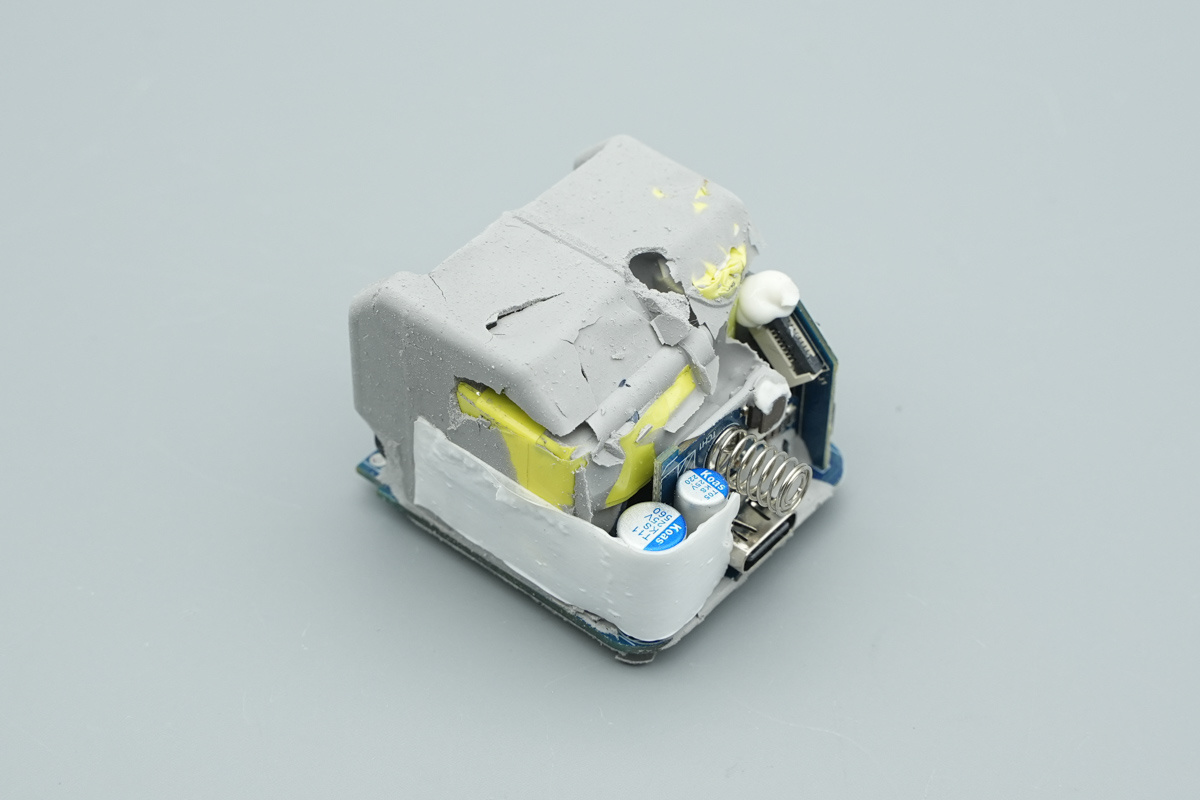
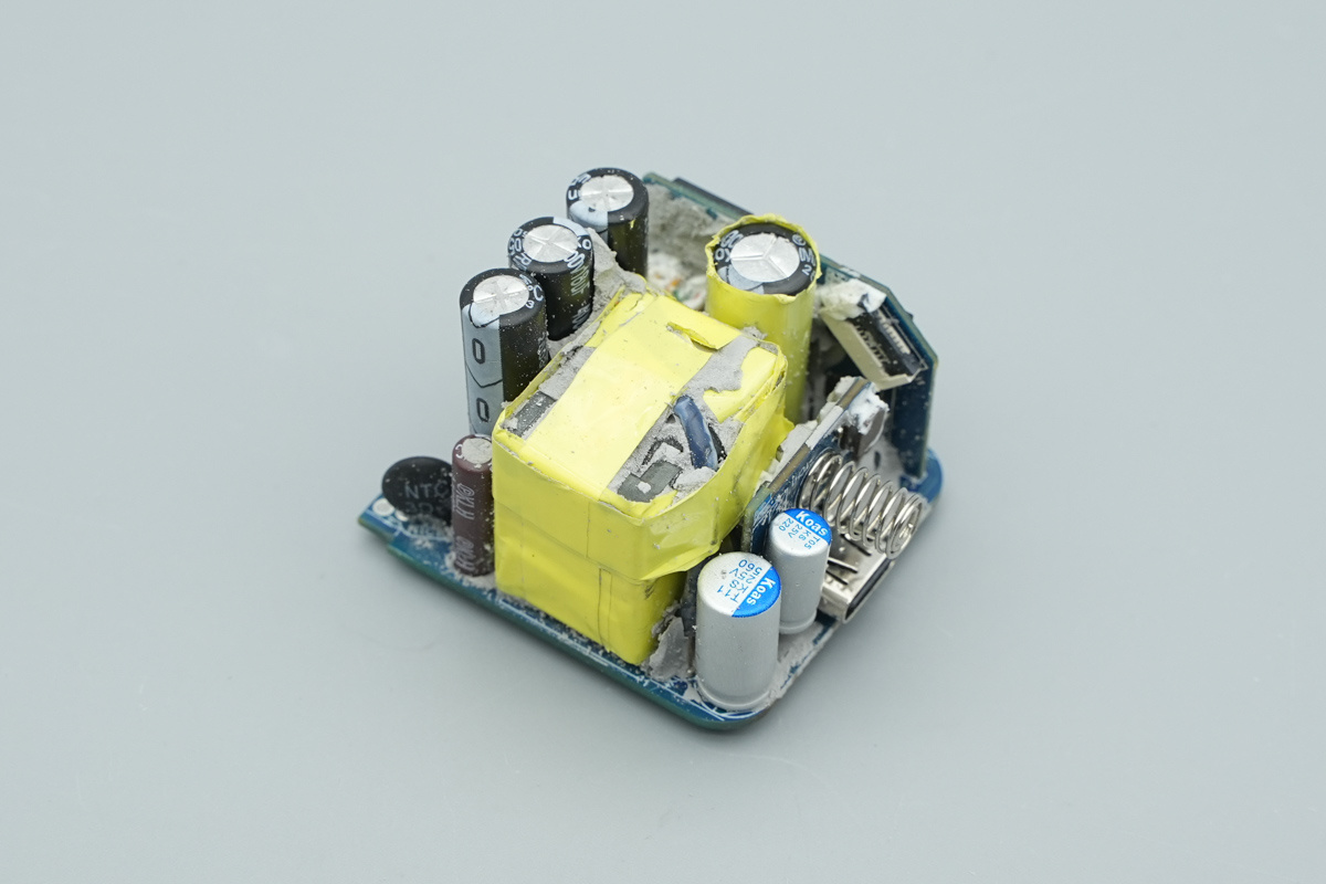
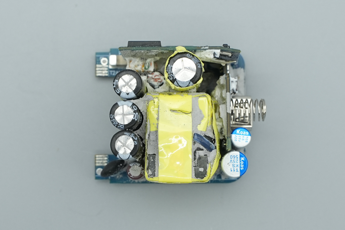
The PCBA is fully covered in gray potting compound, revealing an input capacitor and the touch-sensing spring along its side.
The back of it is likewise fully covered in thermal potting compound.
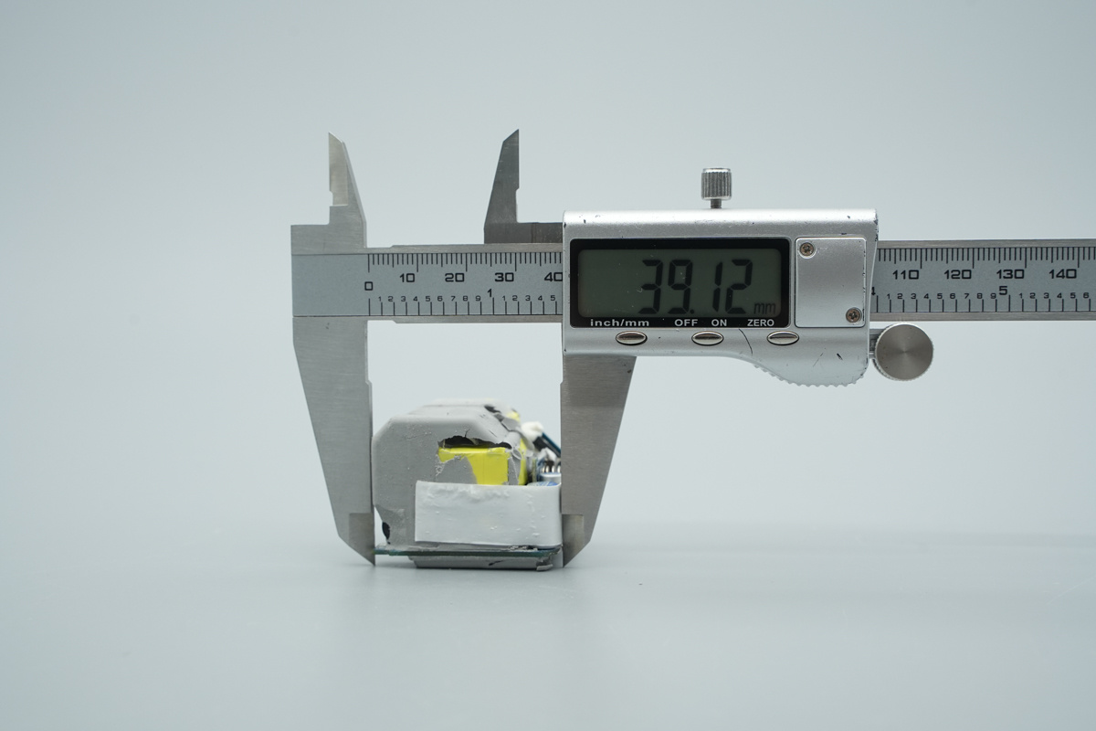
The length of PCBA is about 39.12mm (1.540 inches).
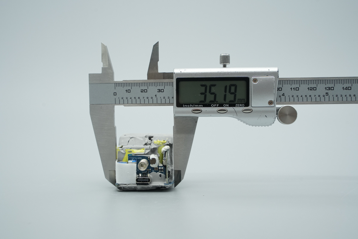
The width of PCBA is about 35.19mm (1.385 inches).
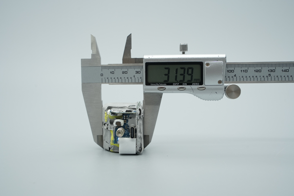
The thickness of PCBA is about 31.39mm (1.236 inches).
With the gray thermal potting compound cleared away, a stacked design is exposed, consisting of a main bottom PCB and two small side PCBs.
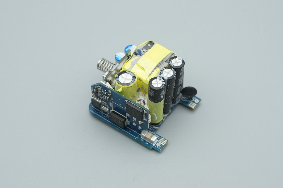
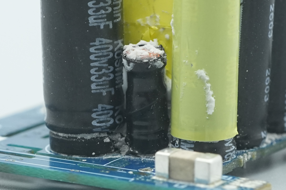
Four input filter electrolytic caps are visible from this angle.
The reverse side displays distinct isolation between the primary and secondary sections.
The front side of the PCBA is populated with the input EMI filtering circuit, input filter caps, the transformer, the output filtering circuit, and the output end PCB.
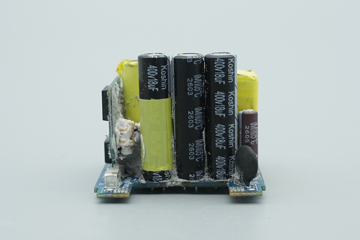
There is the high-voltage filter caps, master control chip power supply cap, and transformer.
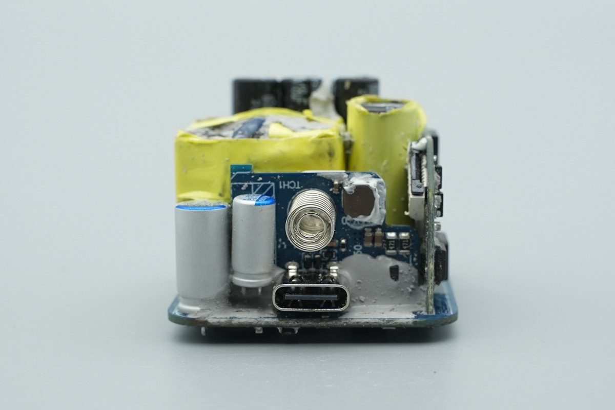
The output end features two solid caps, spring connectors for the screen control ribbon cable, and a centrally located USB-C female port.
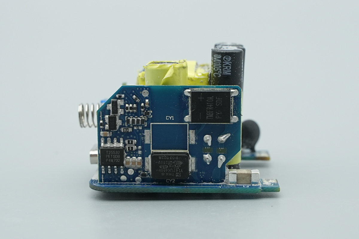
Rectifier bridge and SMD Y-caps located on the side PCB.
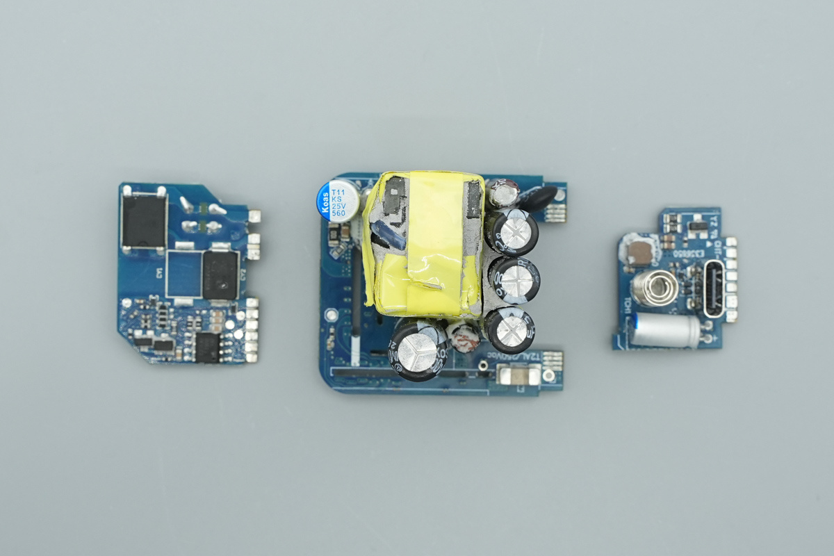
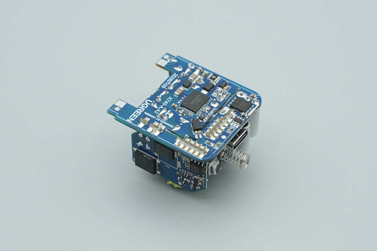
Separating the side PCBs unveils a three-part structure: the left PCB housing the screen driver, the central main PCB featuring the transformer, and the right output PCB.
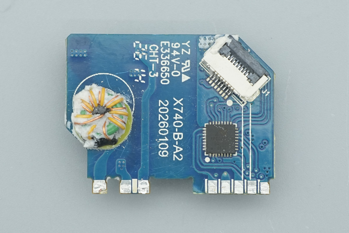
On the front of the left PCB, you will find a common-mode choke, the screen main control MCU, and a socket for the FPC screen ribbon cable.
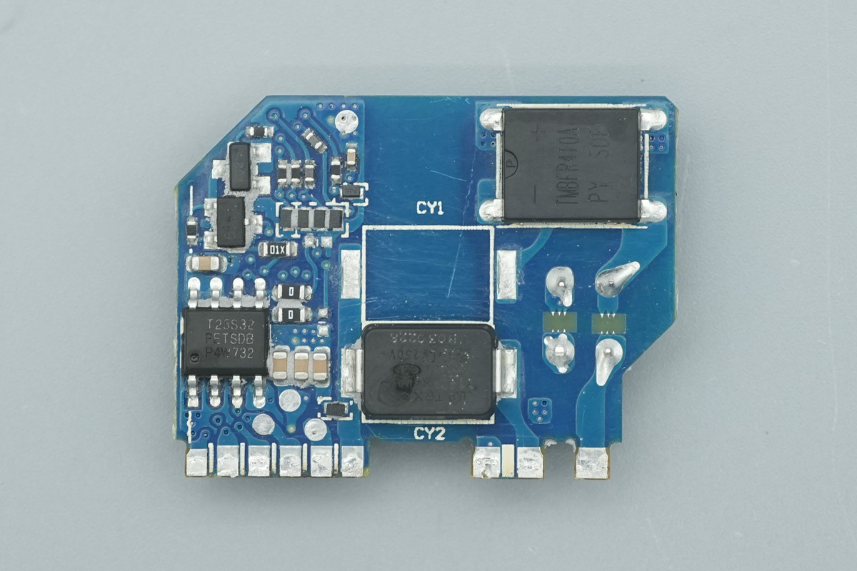
The back of the side PCB houses a rectifier bridge, a memory chip, and SMD Y-caps.
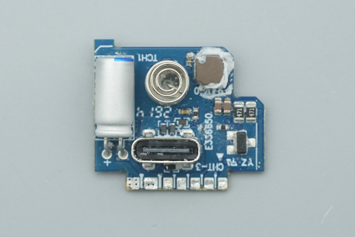
The front of the output interface PCB is equipped with a solid filtering cap, a touch spring, and a USB-C female socket.
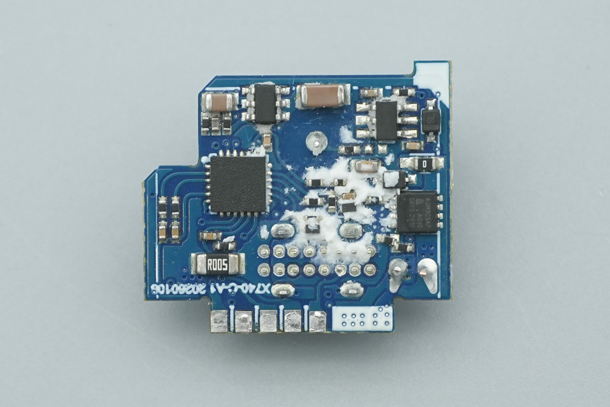
The back side of the output interface PCB is populated with the protocol chip and the output VBUS MOSFET.
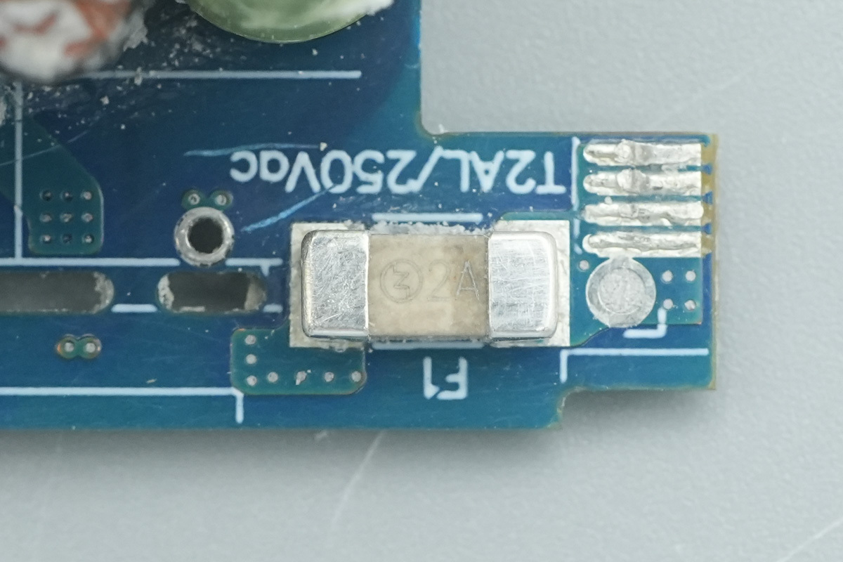
This is a SMD fuse located on the input end.
This is a differential mode choke, insulated with a heat-shrink tube.
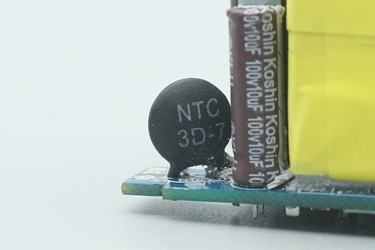
This is an NTC thermistor, employed to suppress inrush current for power-on protection.
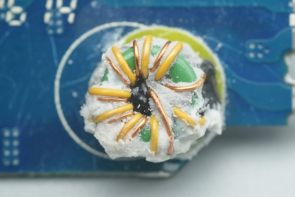
The common-mode choke is utilized to filter out EMI interference.
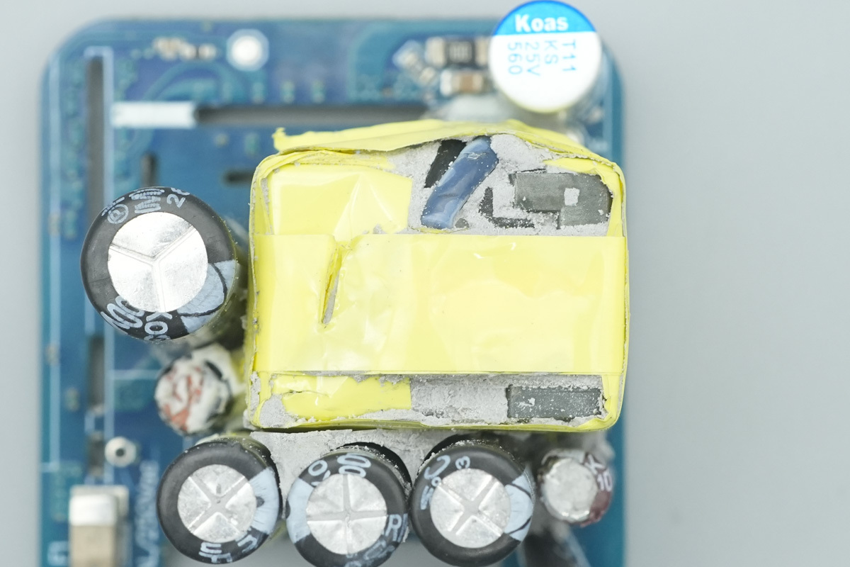
The top of the transformer is wrapped in yellow insulation tape.
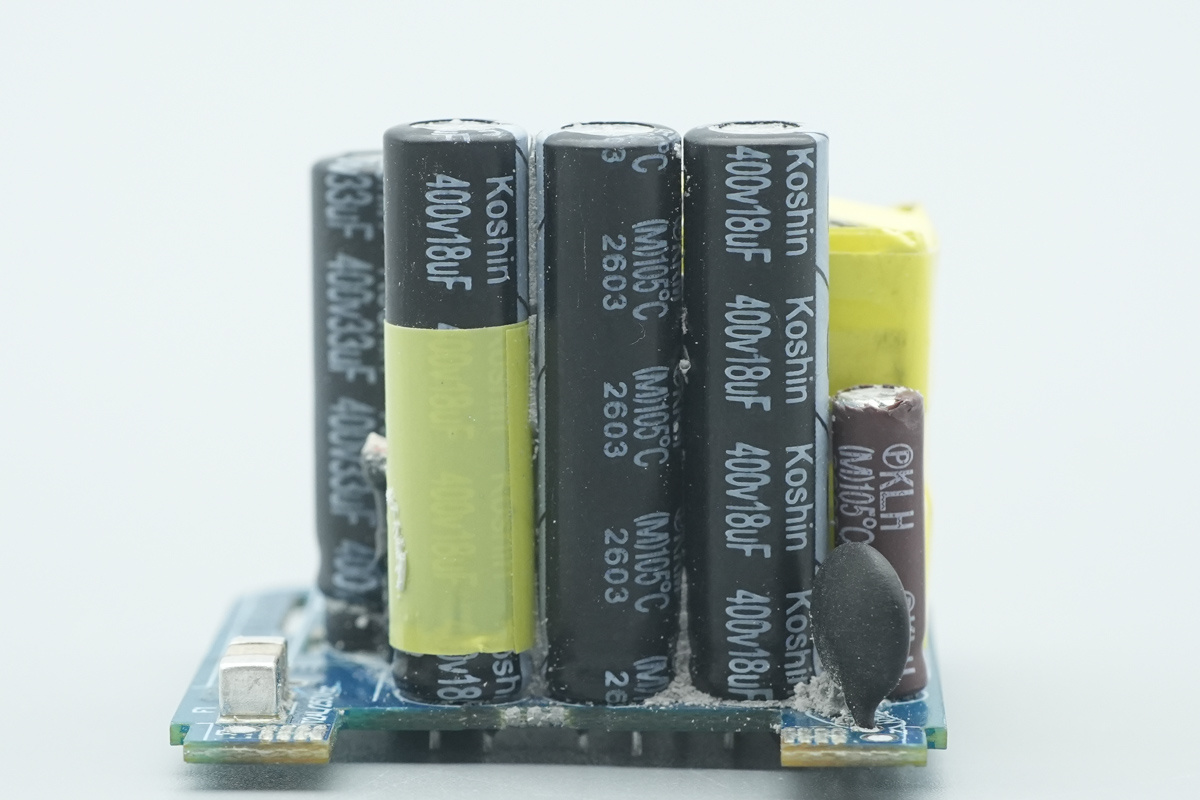
The high-voltage electrolytic filtering caps on the input end are from Koshin, all 400V 18μF.
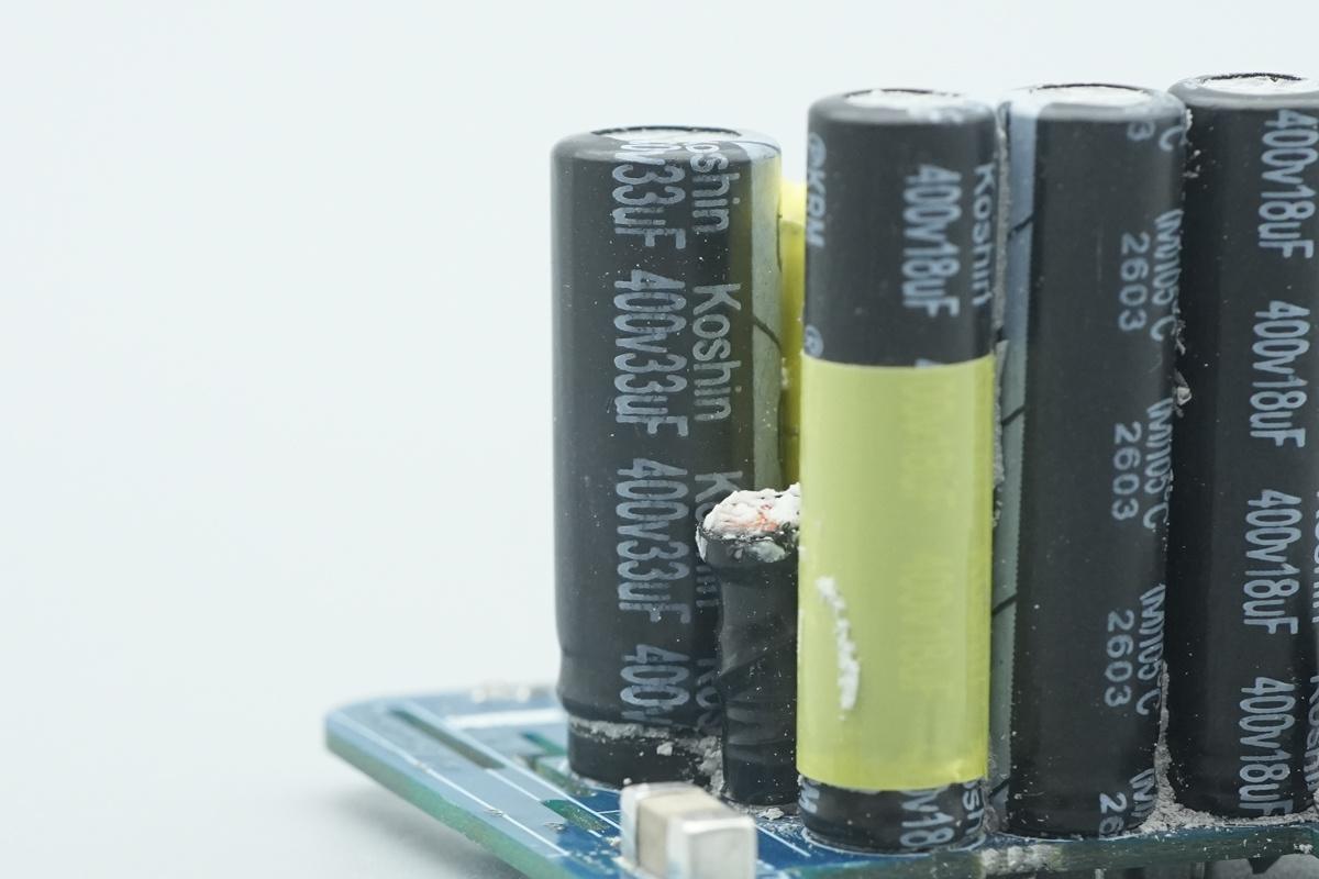
Another one is from Koshin, 400V 33μF.
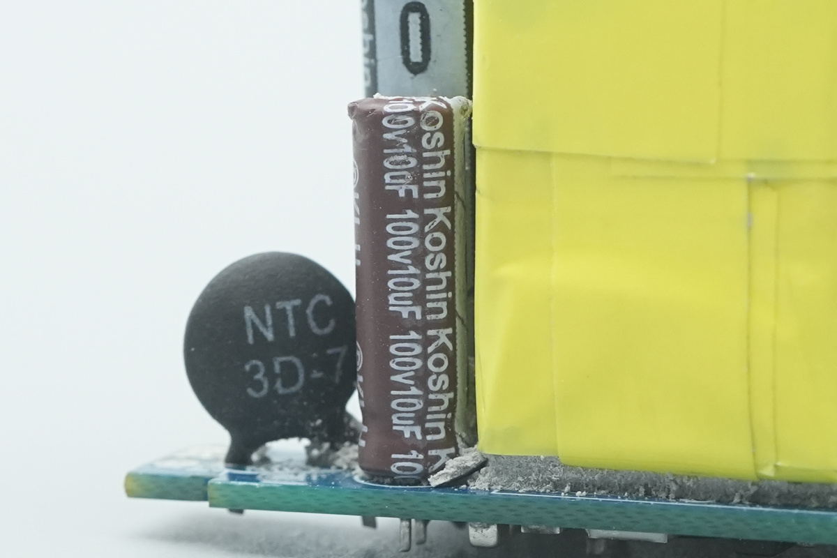
The power supply cap for the master control chip is from Koshin, 100V 100μF.
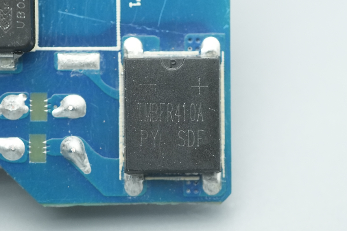
A rectifier bridge, marked TMBFR410A.
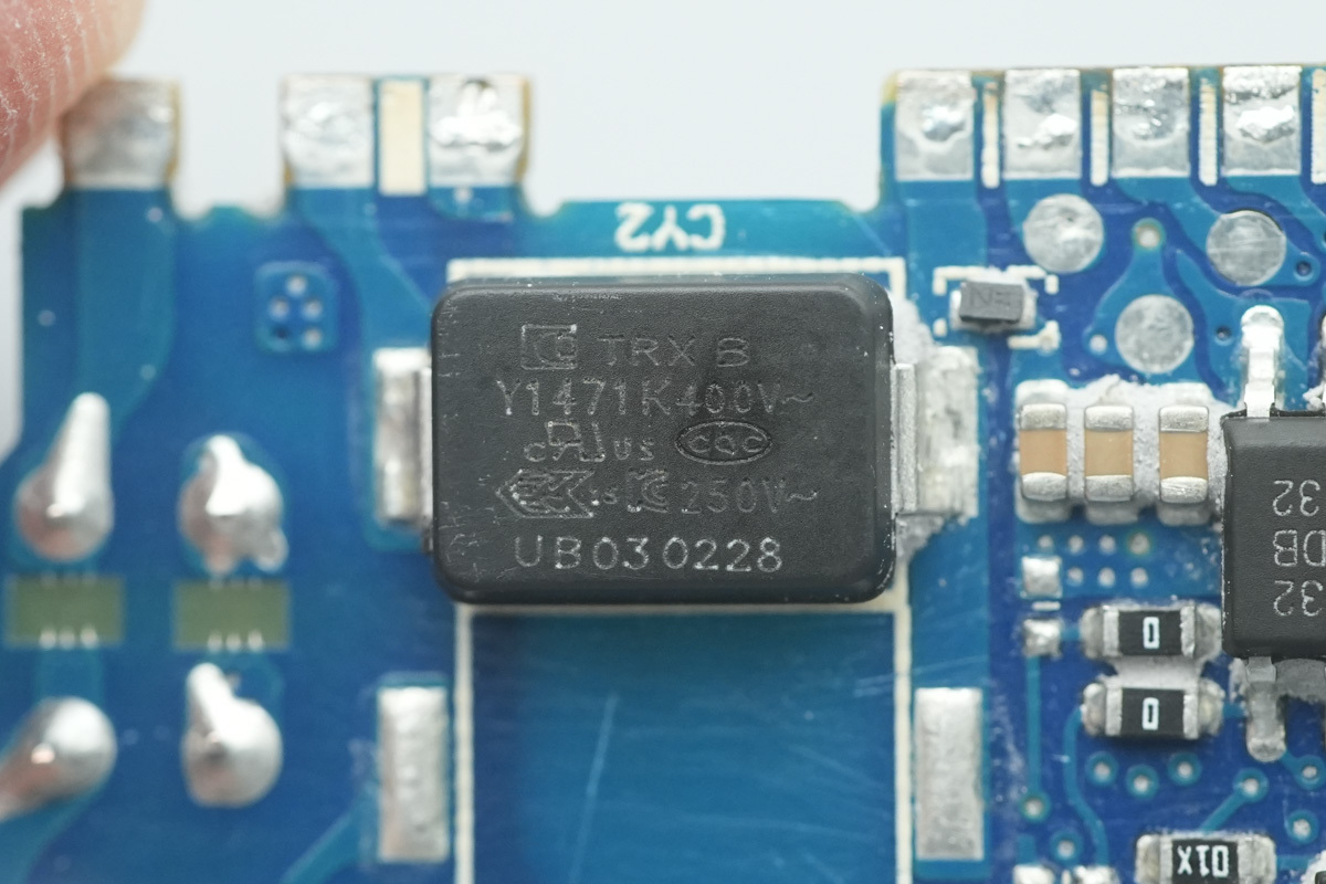
The SMD Y-cap is from TRX, model TMY1471K. Featuring a compact and lightweight design, it is ideally suited for high-density power applications such as GaN fast chargers.
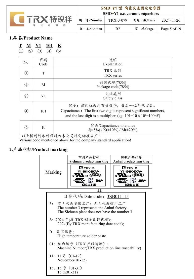
Here is the info about the TRX SMD Y-cap.
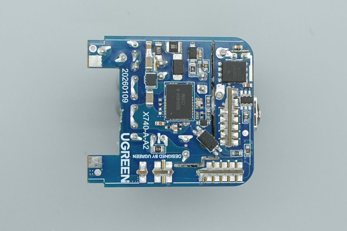
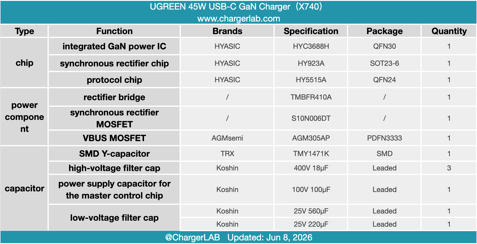
The bottom of the PCBA reveals a space-efficient U-shaped structure consisting of a main PCB and two PCBs, housing the integrated GaN power ICs, synchronous rectifier chips, and their corresponding synchronous rectifier MOSFETs.
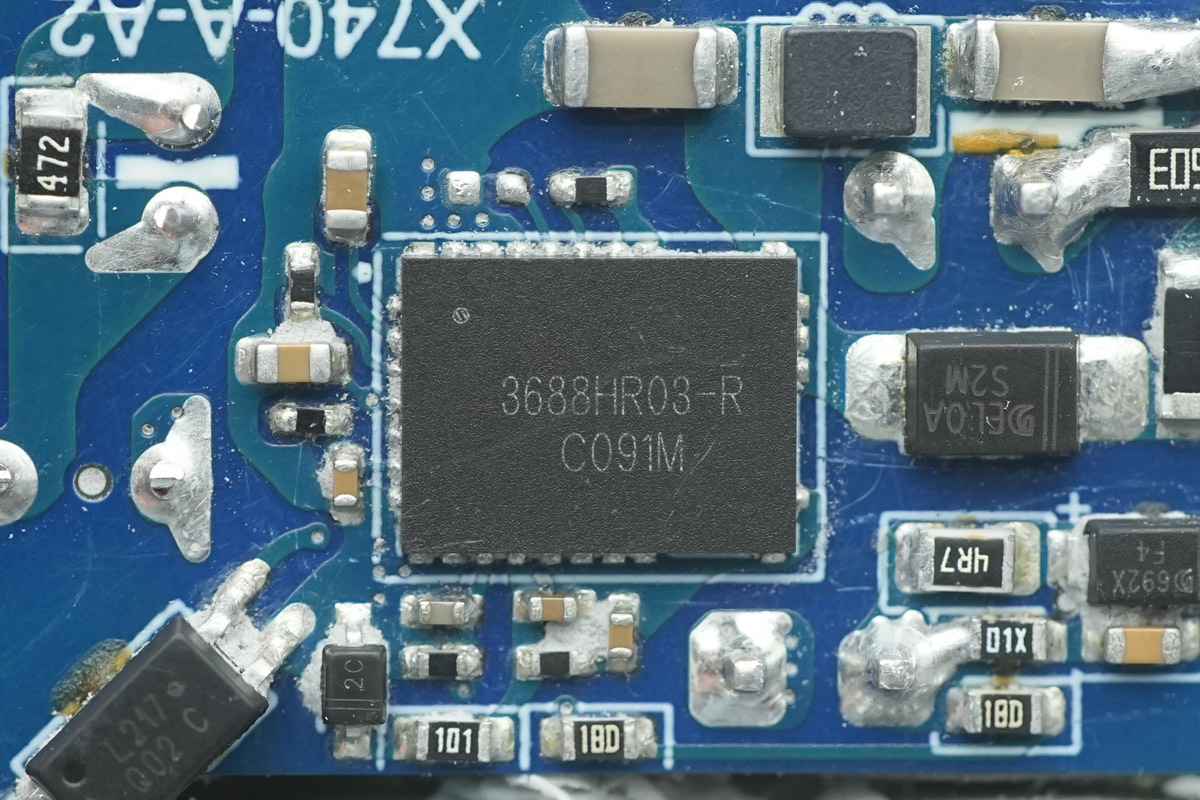
The integrated GaN power IC is from HYASiC, model HYC3688HR02-R. The HYC3688H series is a 3-in-1 controller that integrates the PWM, Sense FET, and GaN.
Utilizing lossless current sensing tech, it integrates high-voltage startup functionality, eliminates the need for conventional sampling resistors, and further improves efficiency while reducing both component count and system costs.
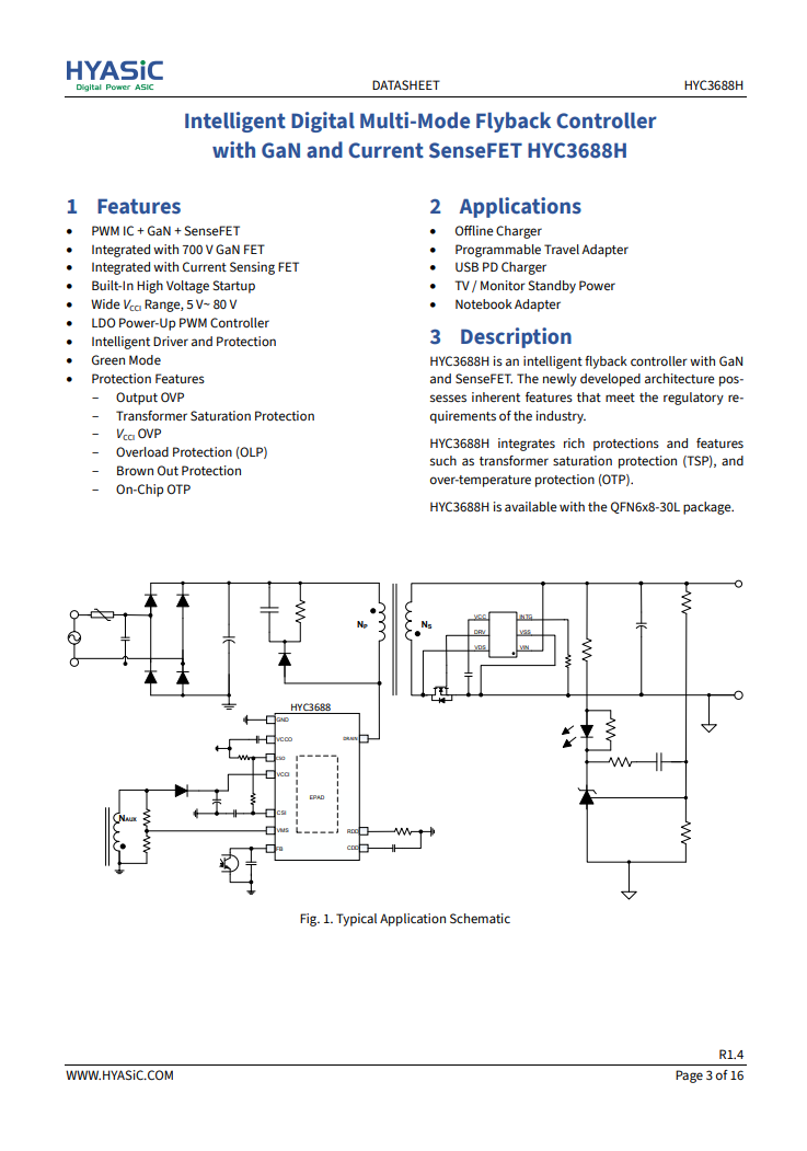
The IC integrates a 700V D-GaN power device, addressing current market demand for miniaturized power supplies. Its proprietary D-GaN drive technology and adjustable switching speed effectively improve radiated EMI performance. It utilizes a 6mm x 8mm DFN package, offering an optimal balance between cost and thermal dissipation. When paired with HYASiC’s synchronous rectifier chip, it ensures stable system operation across CCM, QR, and DCM modes.
The HYC3688H provides comprehensive internal safety protections, including output OVP, transformer saturation protection, overload protection, OTP, and brown-out protection, making it widely applicable for TV/monitor power supplies, USB PD chargers, and laptop adapters.
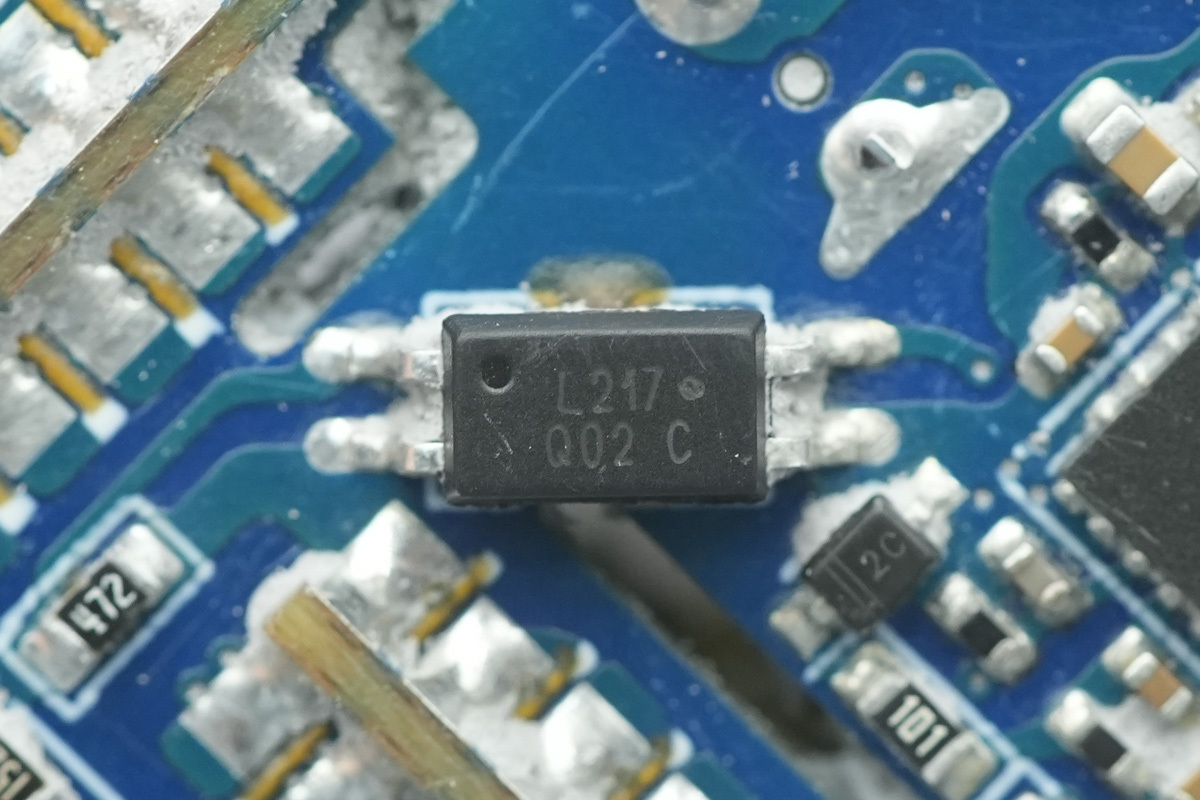
This is a SMD optocoupler used for high-to-low voltage side isolation and feedback, marked L217 Q02 C.
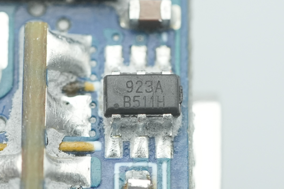
The synchronous rectifier chip is also from HYASiC, model HY923A, in an SOT23-6 package. This intelligent, digitally controlled, multi-mode synchronous rectification controller significantly enhances system efficiency by driving an NMOS to replace the Schottky diode.
It provides flexible support for high-side and low-side synchronous rectification without requiring an auxiliary winding, and it accommodates a wide output voltage range of 3.2V to 25V while supporting high-voltage drain detection up to 150V. Utilizing digital control technology, it is capable of optimized operation across various modes, including DCM, PFM, CCM, and QR, tailored to specific applications.
The core adaptive pre-turn-off scheme ensures rapid state transitions and minimizes switching losses, while also improving system EMI performance through flexible switching turn-off transitions.
Regarding system reliability, the HY923 supports flexible volt-second threshold configuration via the INTG pin, effectively preventing MOSFET mis-triggering due to parasitic ringing in DCM or QR modes. Combined with built-in anti-shoot-through protection and low quiescent current characteristics, this controller is an ideal solution for applications such as PD fast chargers and AC/DC offline adapters.
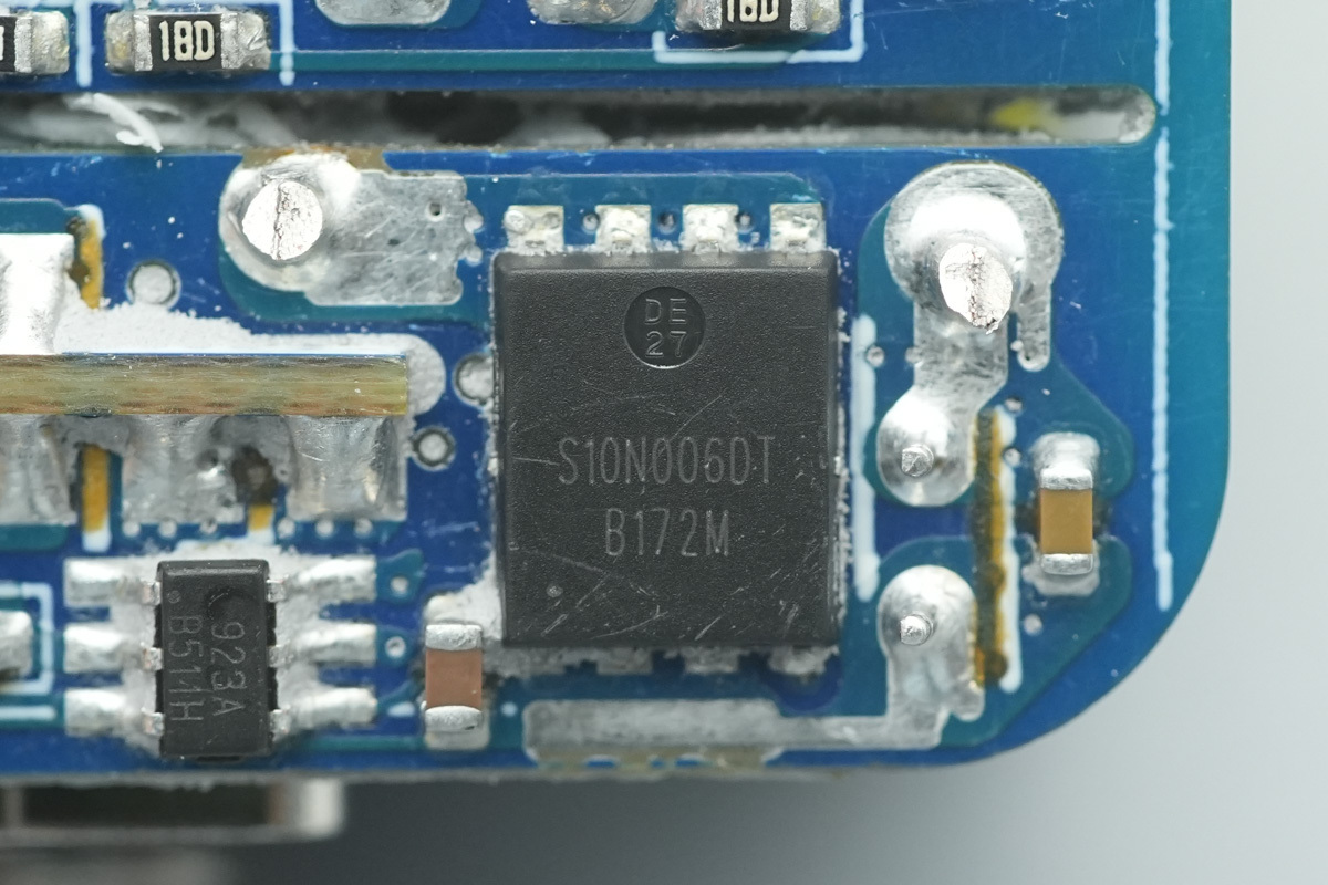
The synchronous rectifier MOSFET, marked S10N006DT.
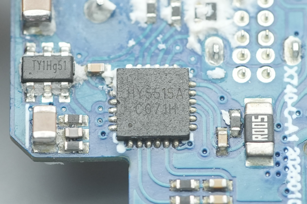
The protocol chip is also from HYASiC, model HY5515A. This cost-effective fast-charging protocol chip features an integrated 32-bit ARM-based MCU, equipped with 32KB of Flash memory and 4KB of SRAM, and is housed in a QFN24 package.
The HY5515A is highly versatile, supporting a wide range of fast-charging protocols including PD 3.2, PPS, QC 3.0+, and UFCS, while also featuring AVS/DPS support, making it specifically optimized for high-performance PD fast chargers. It facilitates I2C and serial communication, enabling the delivery of real-time system telemetry—such as voltage, current, and power levels—to intelligent display interfaces. Furthermore, it is engineered for seamless recognition of the iPhone 15, 16, and 17 series.
To ensure system-level robustness, it integrates a comprehensive suite of programmable protection features, including over-voltage, under-voltage, over-current, and over-temperature protection, complemented by advanced ESD shielding to guarantee long-term reliability.
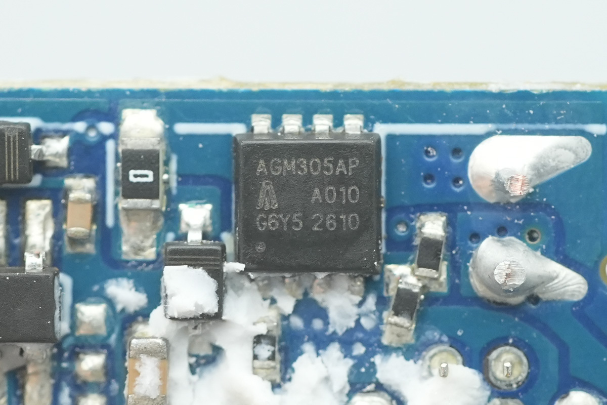
The VBUS MOSFET is from AGMsemi, model AGM305AP, 30V and 4.5mΩ, housed in a PDFN3333 package.
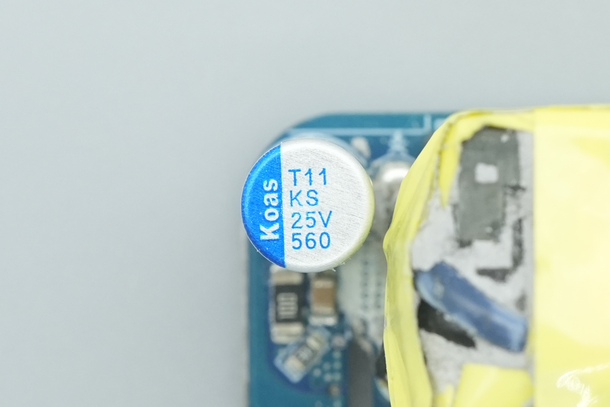
The solid filtering cap at the output end is from Koshin, 25V 560μF.
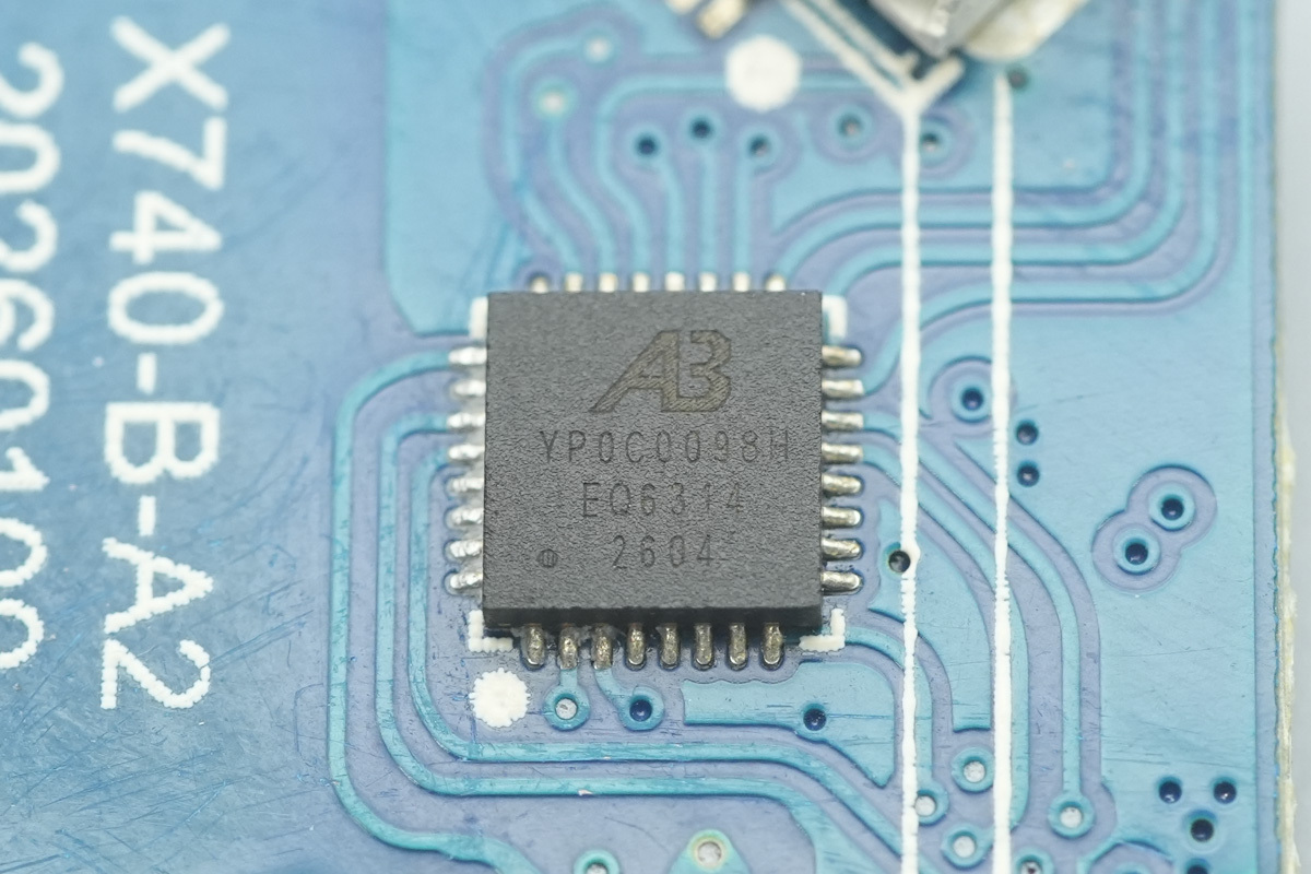
The MCU serves as the dedicated controller for the charger’s display UI and real-time parameter interaction, marked YP0C0098H.
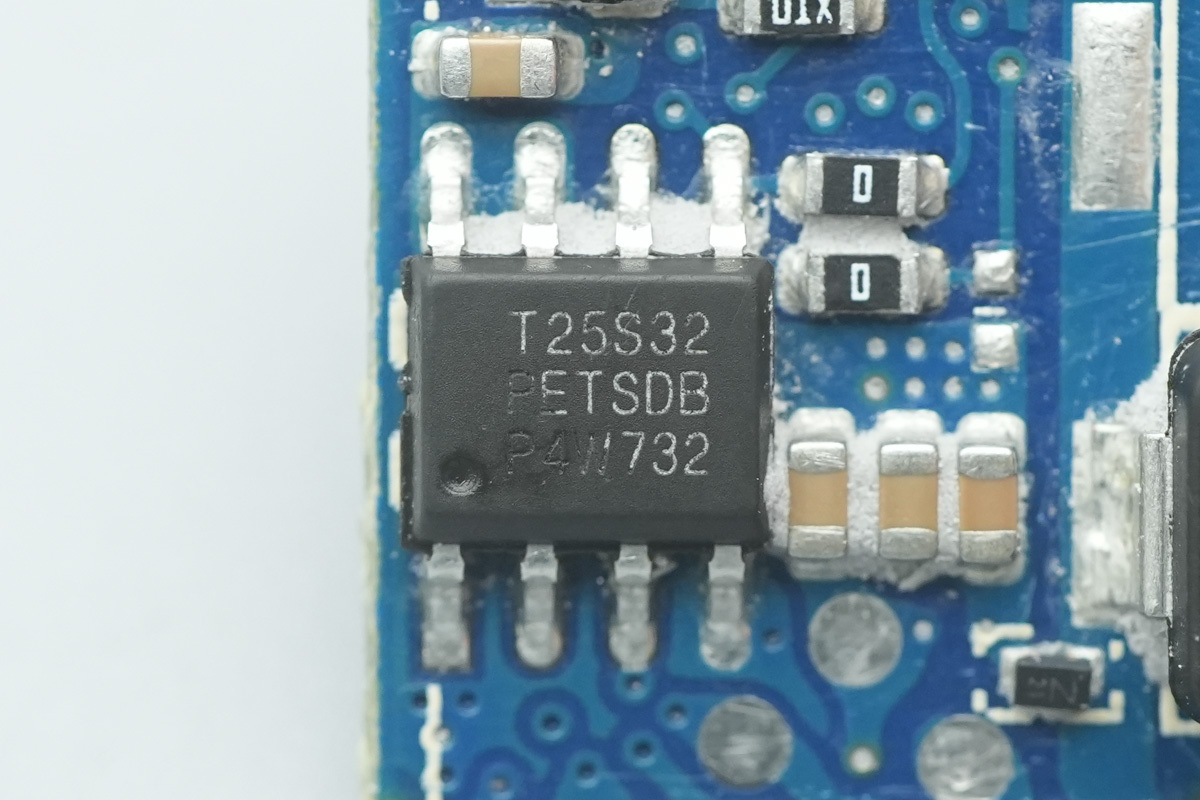
The NOR flash is from First-Rank, model T25S32, housed in an SOIC8 package, to firmware storage for the controller.
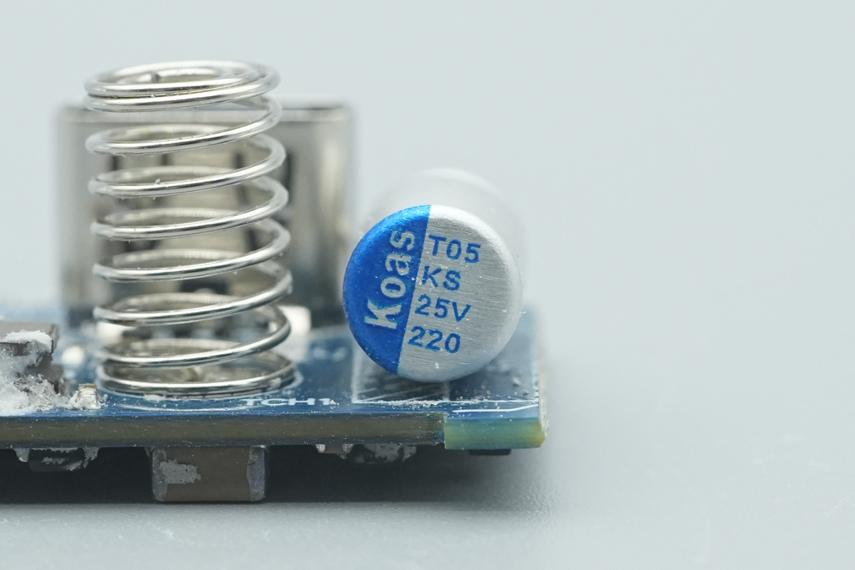
Another output solid filtering cap is from Koshin, 25V 220μF.
The USB-C female receptacle features a black internal plastic sheet.
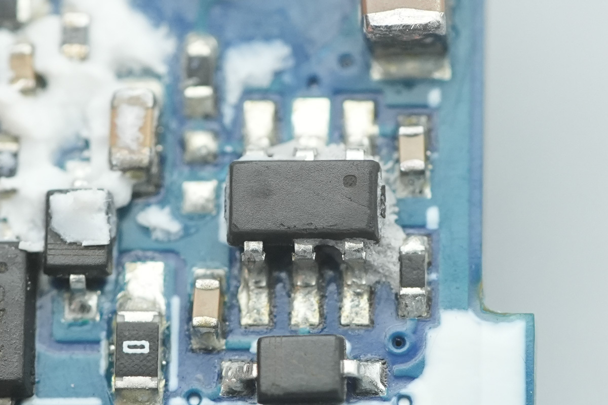
A chip with no mark.
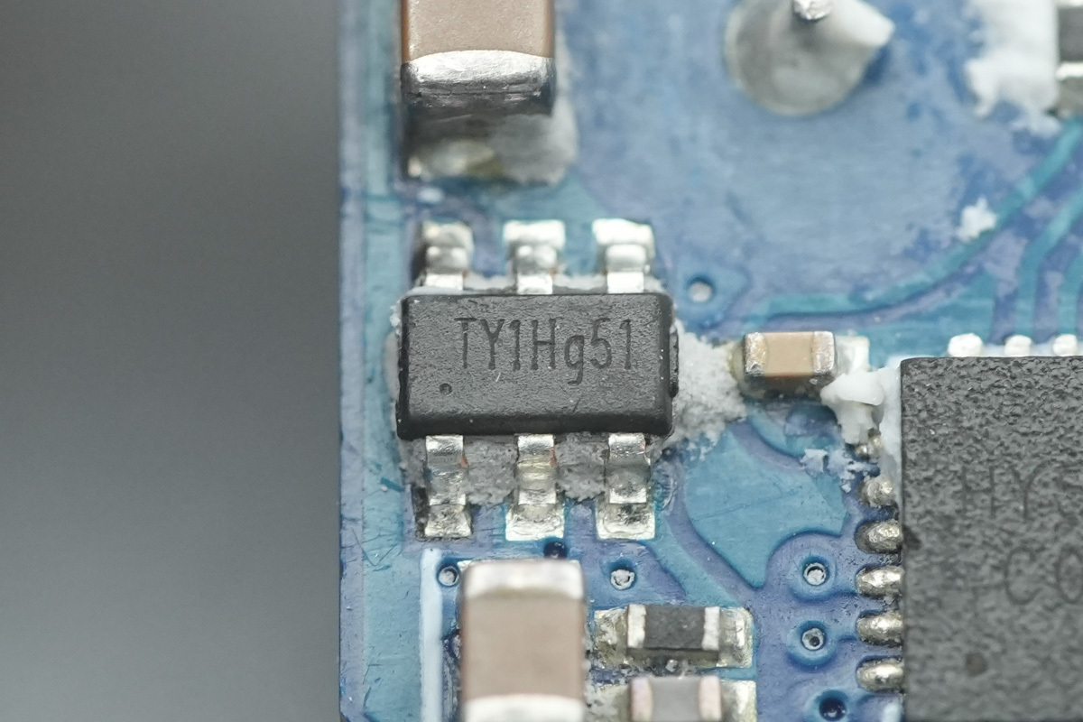
A chip, marked TY1Hg51.

Well, those are all components of the UGREEN 45W USB-C GaN Charger.
Summary of ChargerLAB
UGREEN’s 45W USB-C GaN charger redefines the power adapter by adding a tilted micro-display. It offers more than just power, providing users with live data monitoring—including wattage and temperature—and customizable animations, making it both a practical tool and a stylish desk accessory.
To pack 45W of fast-charging power and a display controller into such a small form factor, UGREEN employed a dense, multi-board stacked structure filled with thermal potting compound, balancing efficient heat management with rugged durability.
The internal specs are equally impressive: HYASiC provides the integrated GaN main controller, synchronous rectification, and protocol chips. Other key components include Koshin caps and TRX SMD Y-caps, complemented by an onboard MCU and storage system for the UI. In short, UGREEN has delivered a meticulously designed, high-performance charger that pushes the boundaries of quality and innovation.
Related Articles:
1. Teardown of UGREEN Nexode Air 45W GaN Charger (X840)
2.One-Tap Battery Health Check:UGREEN P6 Series 45W Power Bank with Integrated Cable Now Available in China
3. Unboxing of UGREEN Nexode 500W GaN Charger