Introduction
We are taking a look at the Baidu Kunlunxin K200, a full-height, dual-slot AI accelerator card built on the 1-Gen Kunlunxin chip. Supporting PCIe Gen4 x8 (with full backward compatibility), this card is built on the XPU-K architecture using a 14nm process. With 16GB of HBM memory providing 512GB/s bandwidth, it is a formidable piece of hardware.
The K200 is versatile, supporting INT8/INT16/INT32 and FP16/FP32 precision for both AI training and inference. Housed in a sleek black aluminum alloy casing, the card relies on an internal passive heatsink optimized for server-grade airflow. Join us as ChargerLAB breaks down the Baidu Kunlunxin AI accelerator to reveal its internal engineering and build quality.
Product Appearance
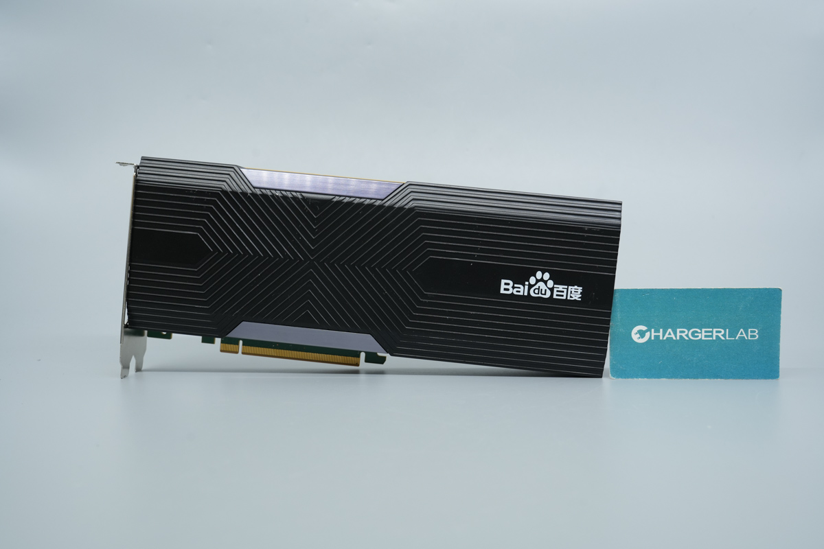
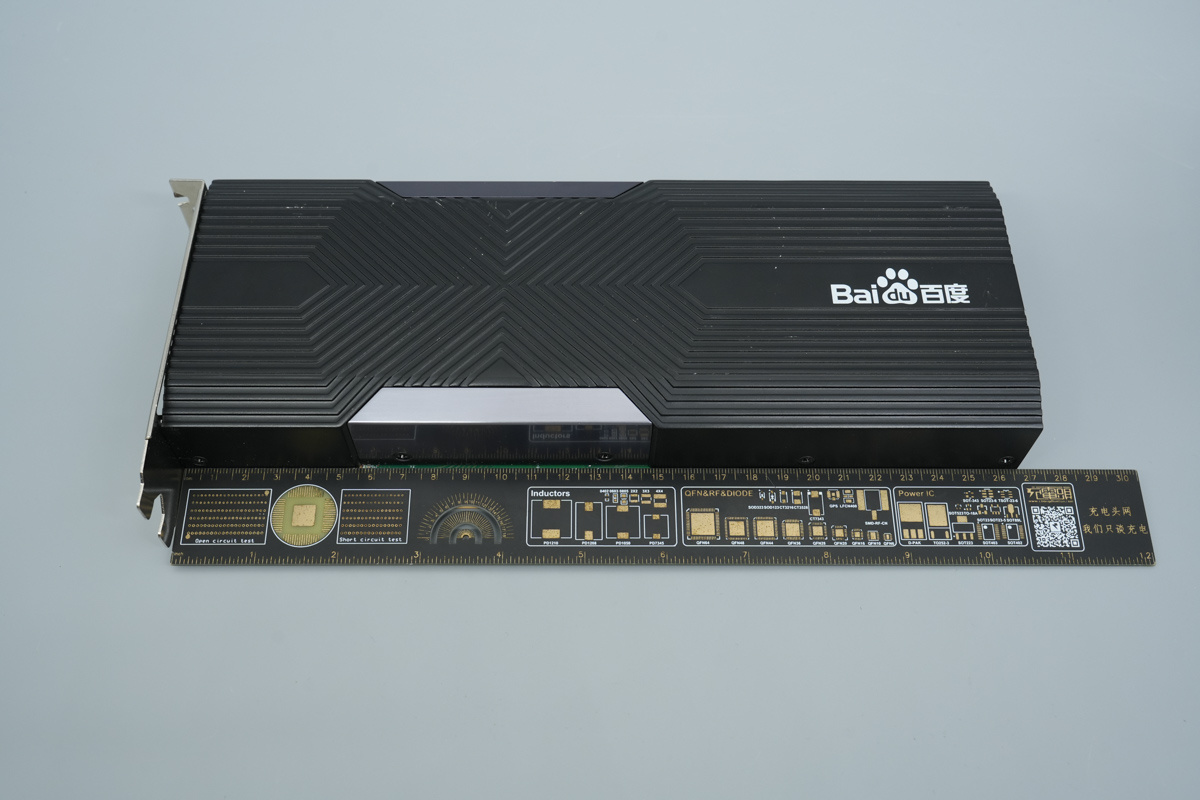
Encased in black aluminum alloy, the Baidu Kunlunxin accelerator card prominently displays the Baidu logo on its right panel.
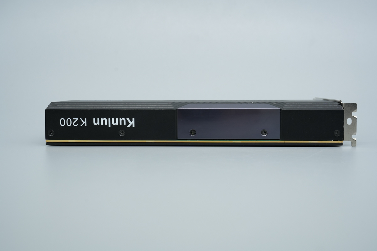
The model name "Kunlun K200" is clearly marked on the top of it, and features securing screws.
Additional securing screws located on the bottom edge.
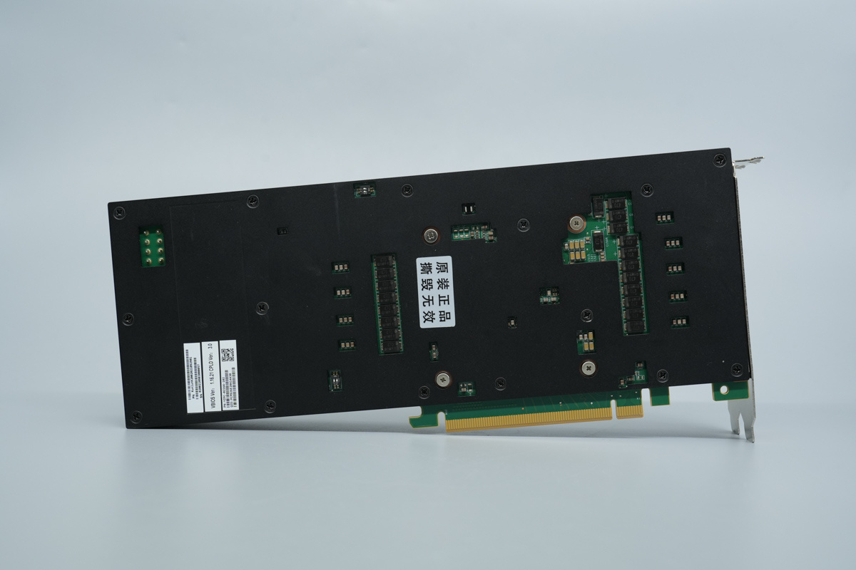
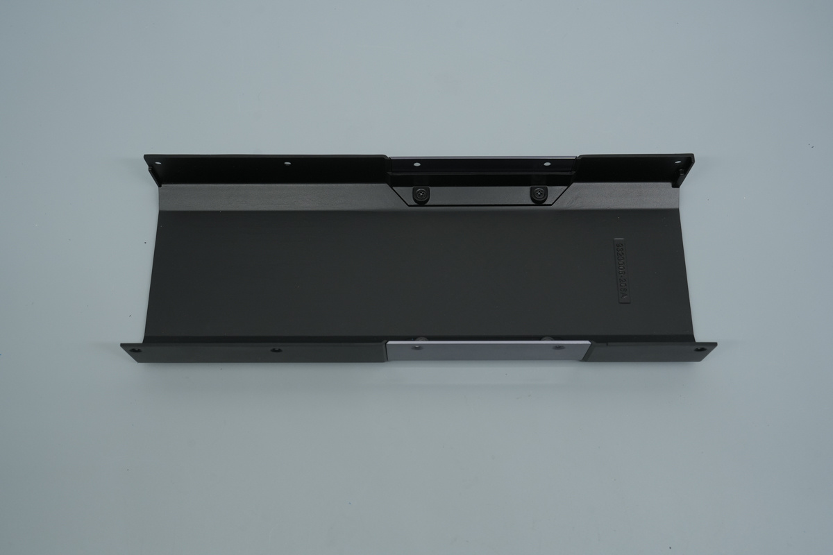
The back of it is equipped with an aluminum alloy backplate, which is secured by screws and features labels for the model and serial number. The backplate includes cutouts corresponding to the cap locations to reduce its overall thickness.
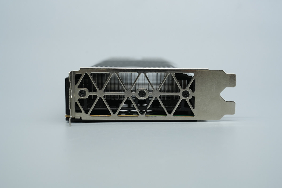
It’s side panel is ventilated with a through-flow design, facilitating cooling via high-velocity system airflow.
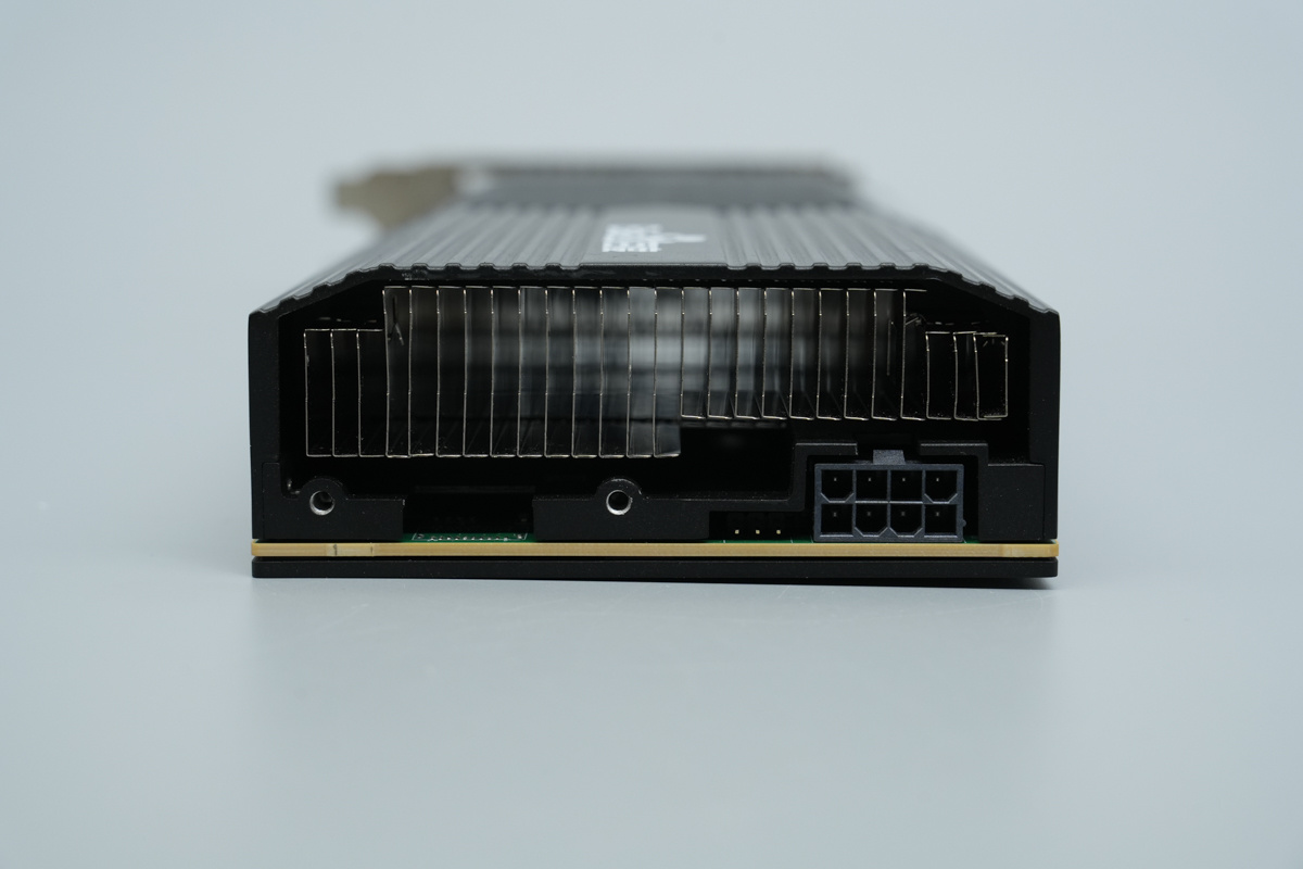
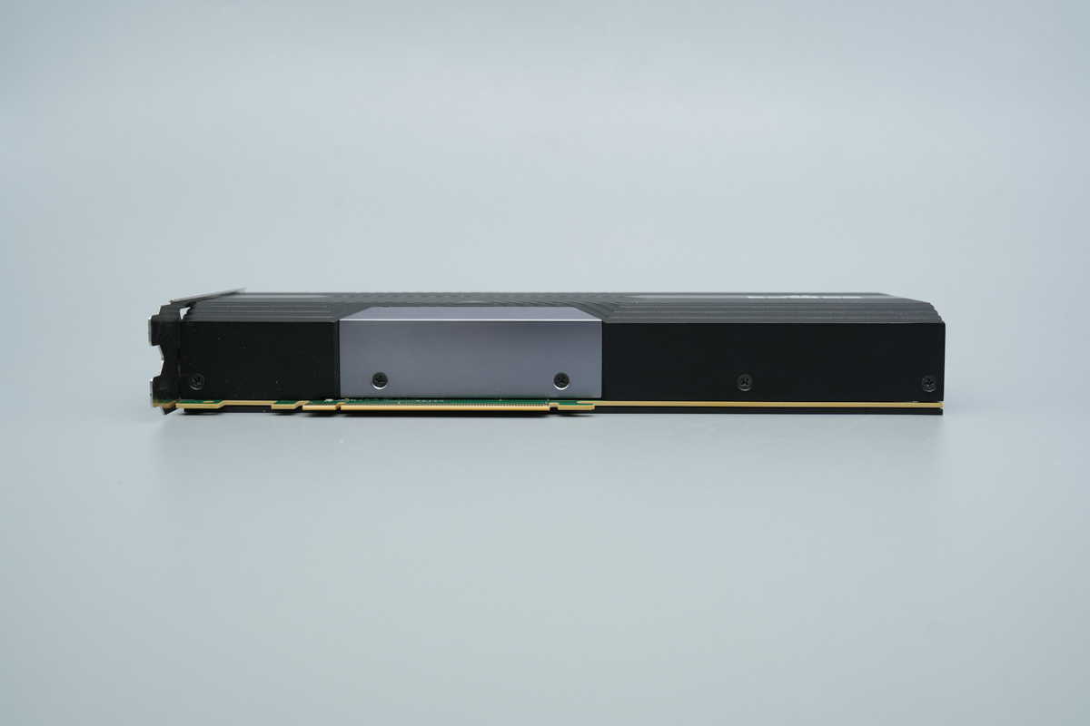
The opposite side of it is equipped with heat dissipation fins and power input connectors.
The length of the accelerator card is about 267mm (10.512 inches).
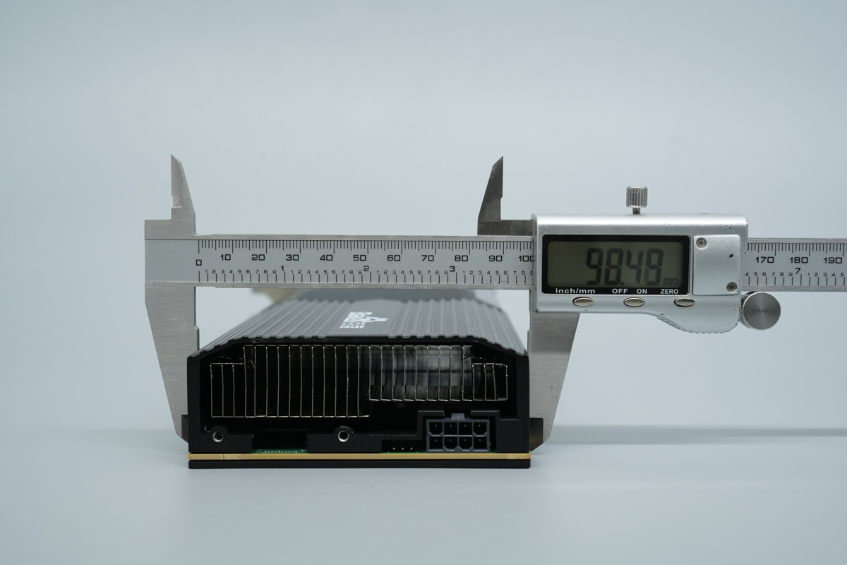
The width of the accelerator card is about 98.5mm (3.878 inches).
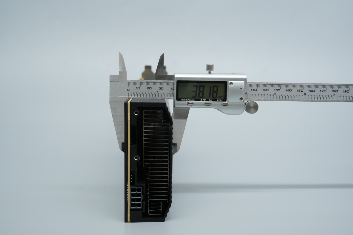
The thickness of the accelerator card is about 38.2mm (1.504 inches).
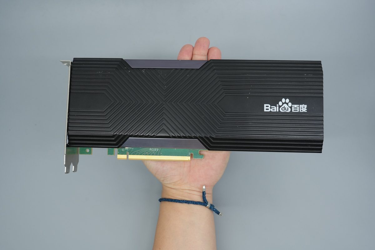
That's how big it is in the hand.
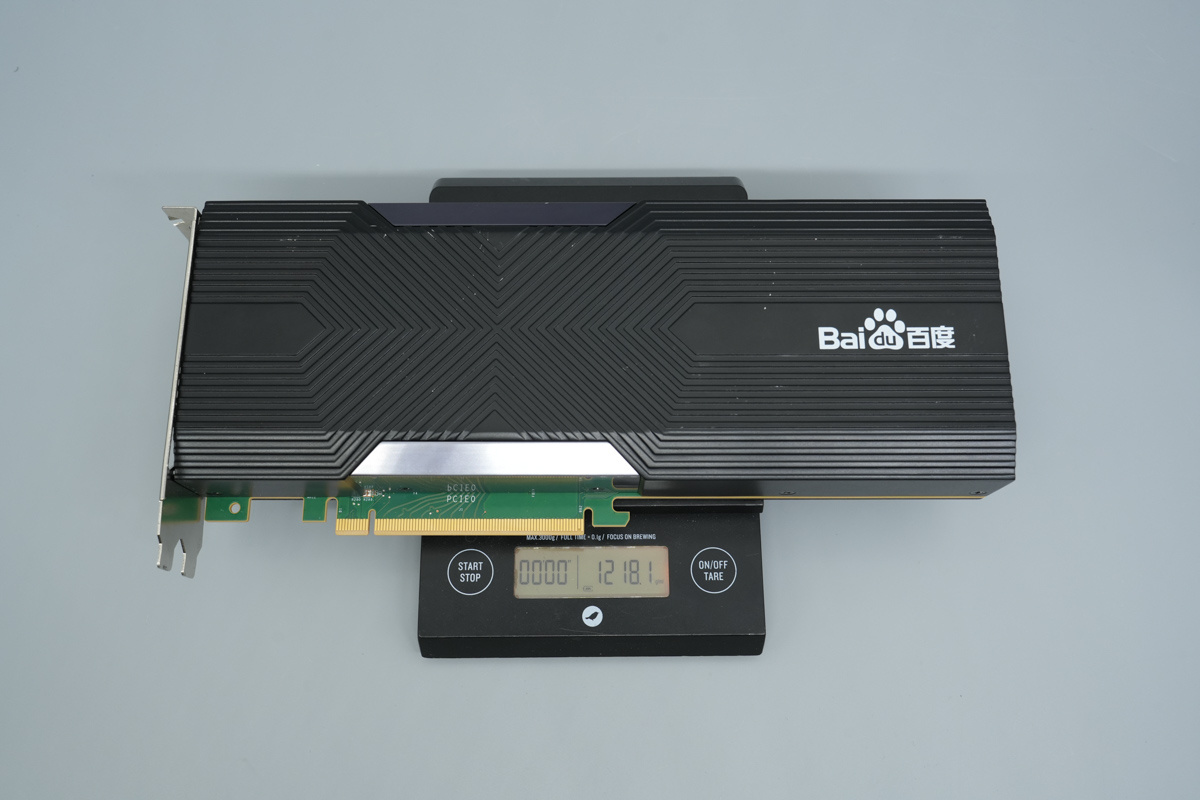
The weight is about 1218g (42.96 oz).
Teardown
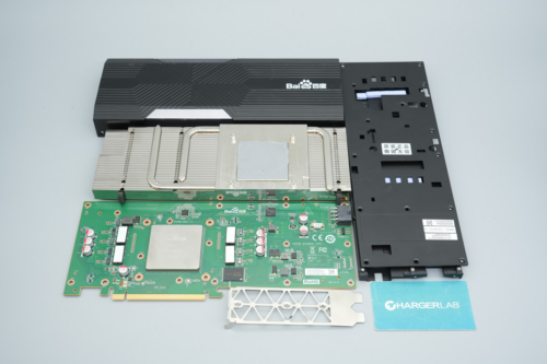
With the exterior tour concluded, it is time to crack open the Baidu Kunlun AI accelerator and take a closer look at its internal engineering and component quality.
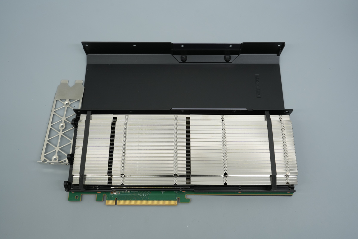
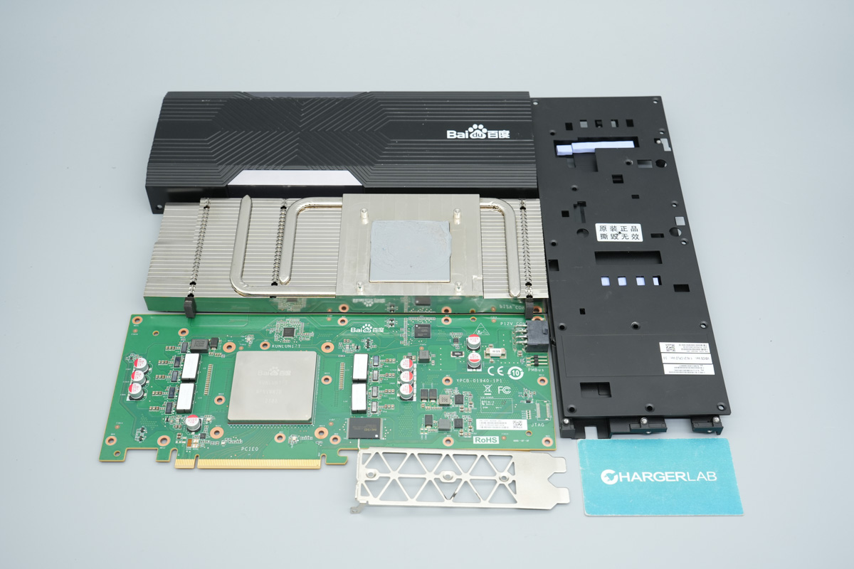
First, unscrew the retaining screws located on the back of the accelerator card, and then remove the front enclosure.
The enclosure is constructed from aluminum alloy.
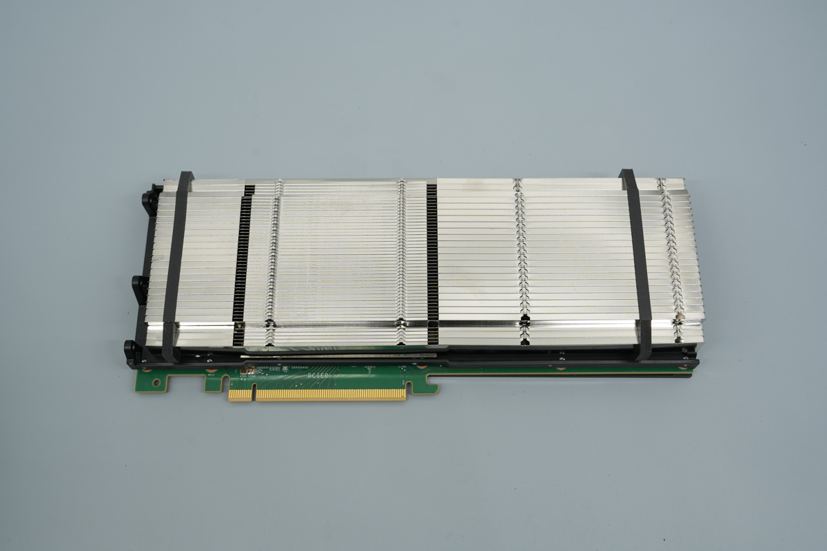
The PCBA module is covered by a large-area heatsink.
Unscrew the retaining screws from the backplate and remove it. The heatsink is secured in place by additional screws.
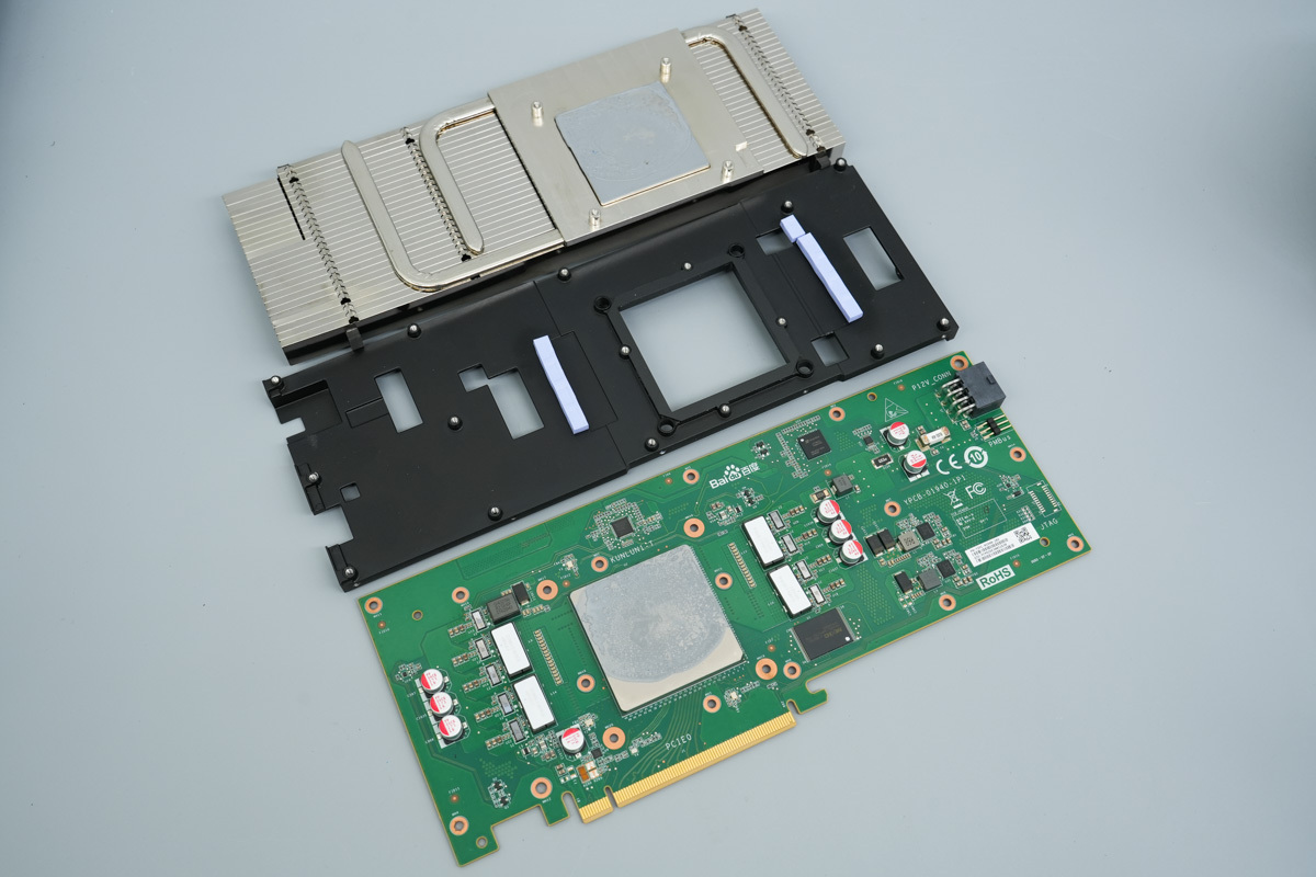
Unscrew the retaining screws and remove the heatsink and the middle frame. Thermal grease is applied to the core for heat dissipation, while thermal pads are used to dissipate heat from the smart power stages.
The central-left area of the PCBA features the accelerator card's core, flanked by power chokes, smart power stages, and filtering caps. A power controller is situated above the core. The right side accommodates the hardware management controller, voltage and current monitor, synchronous step-down chip, filtering caps, and a fuse.
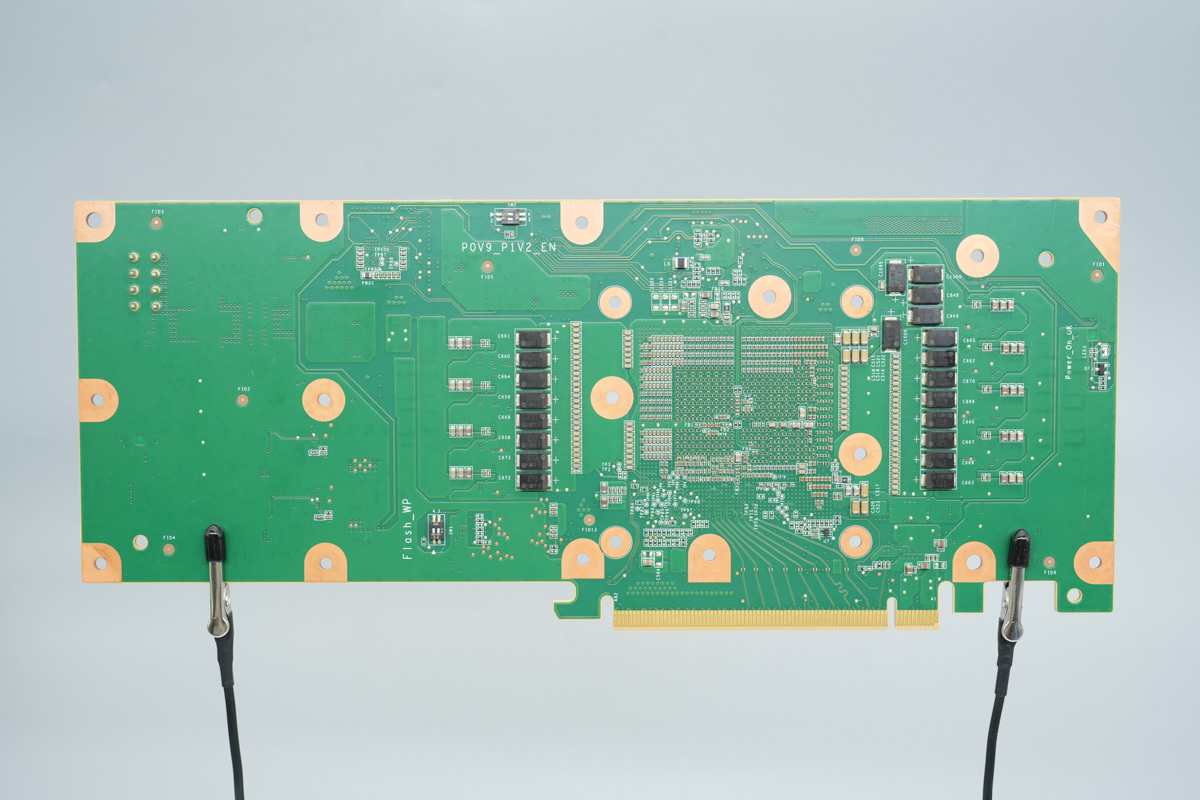
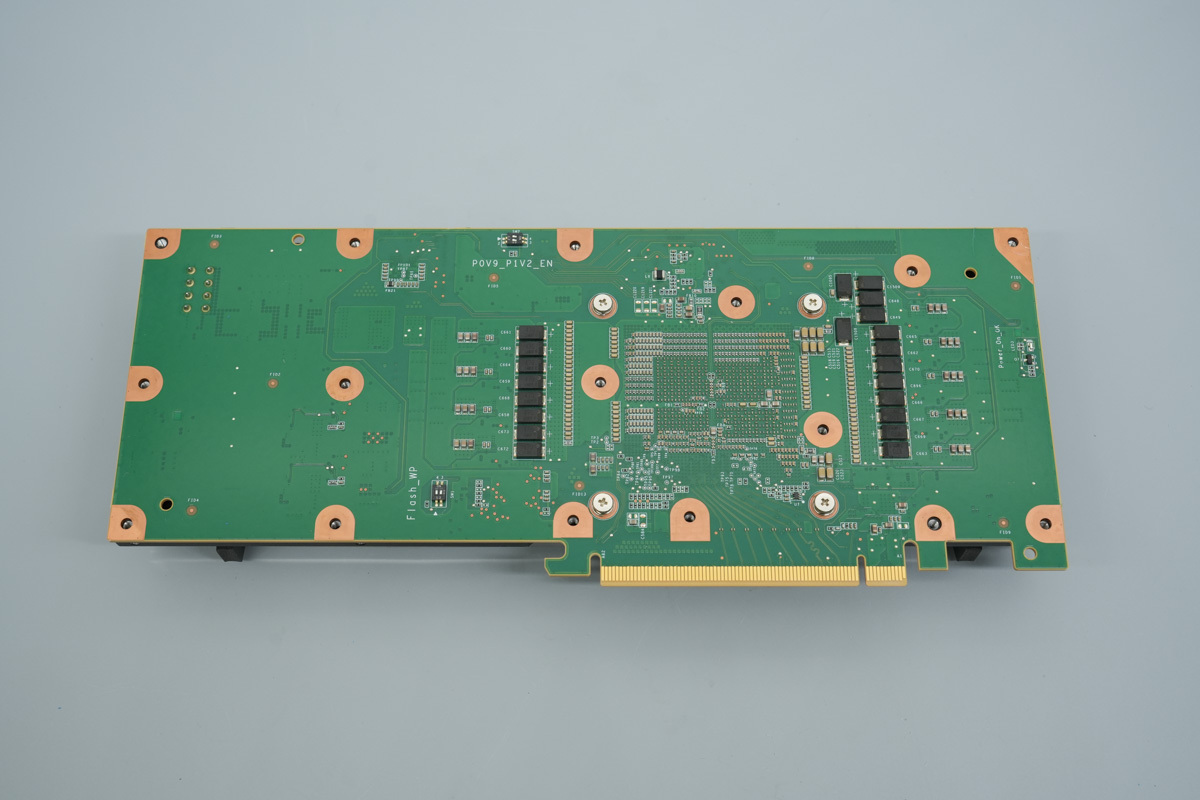
The back of the PCBA is equipped with filtering caps and DIP switches.
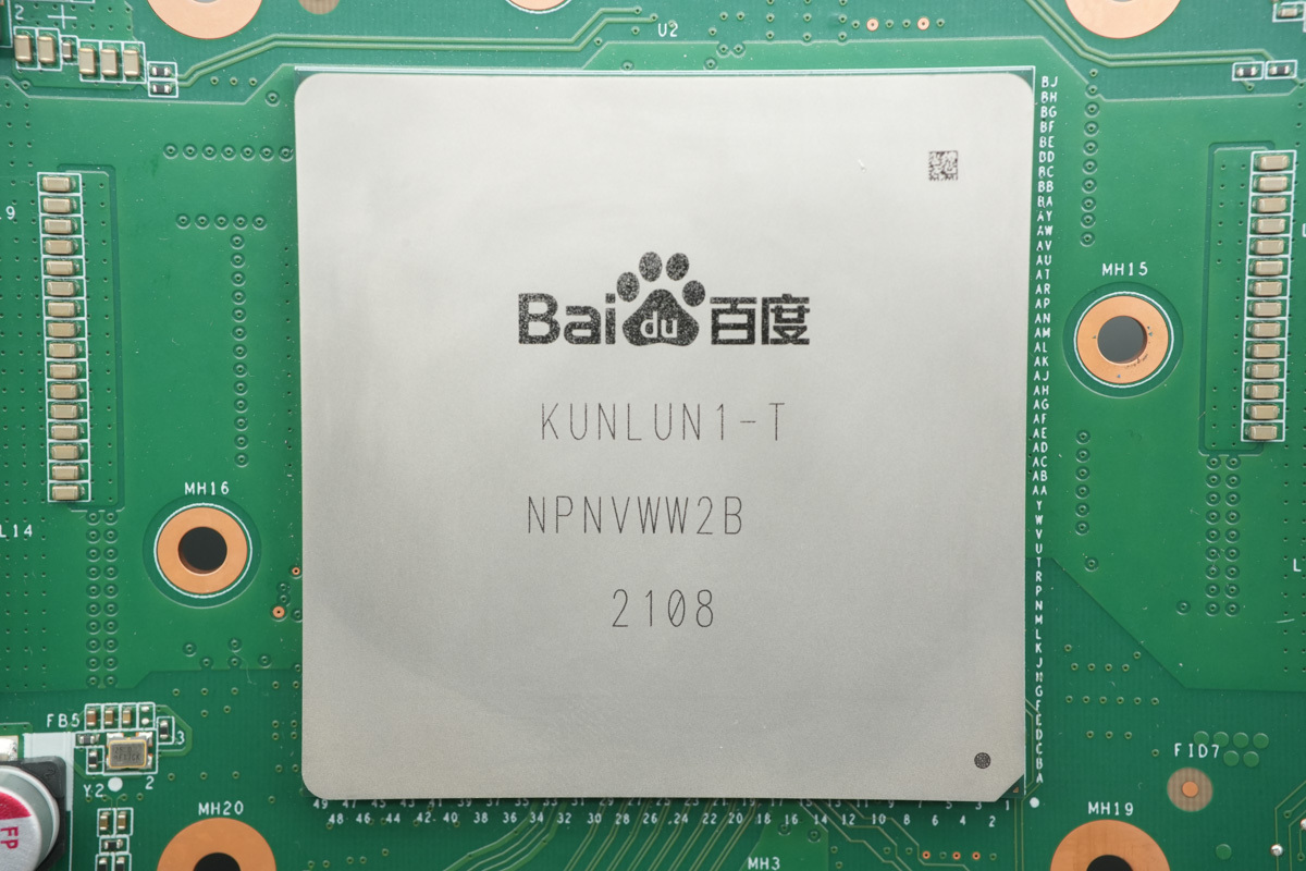
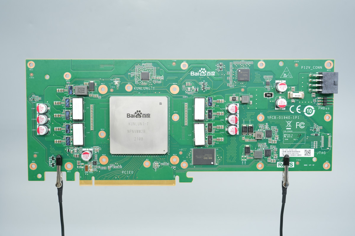
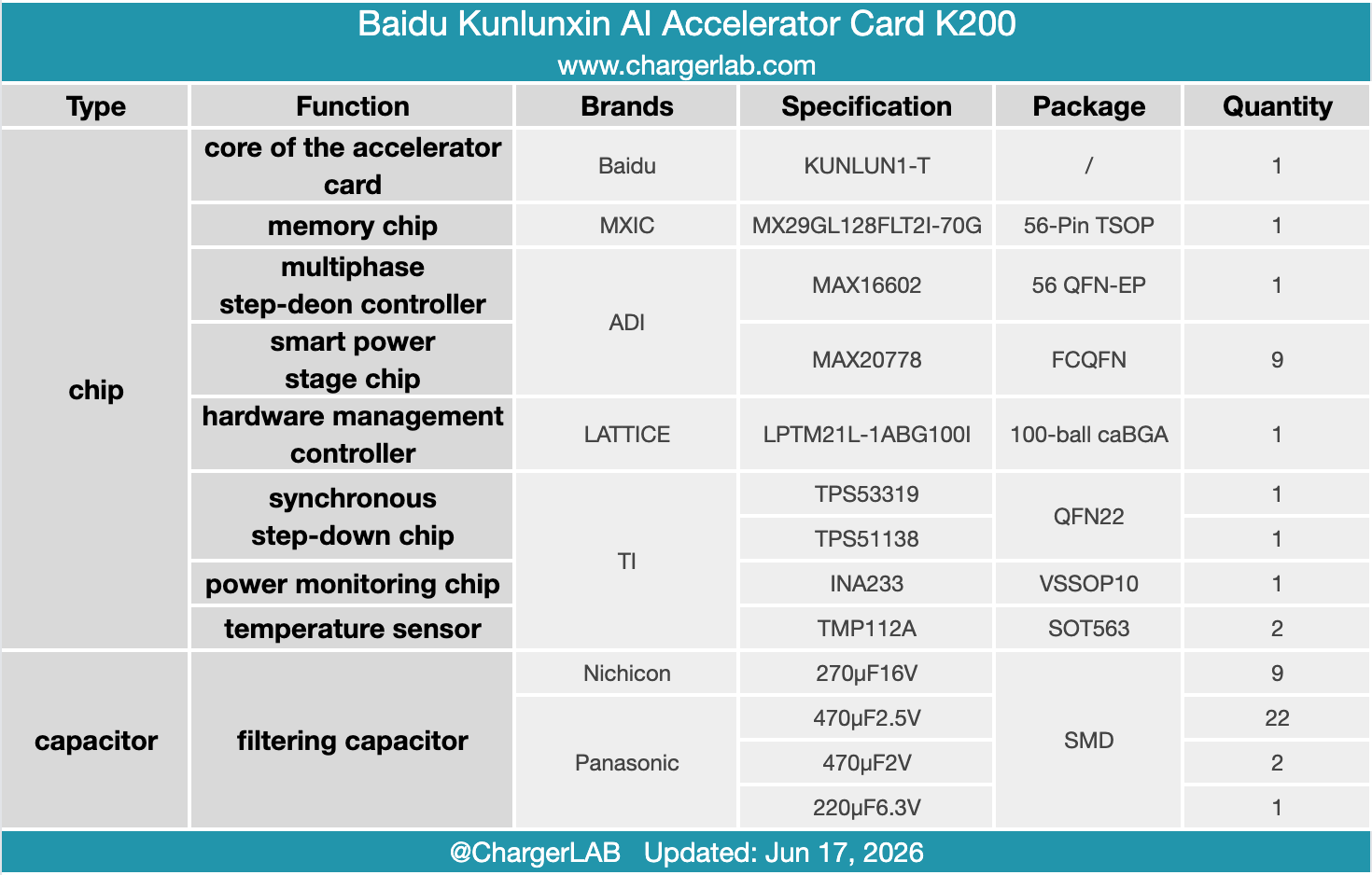
The core of the accelerator card is protected by a metal casing, printed with the Baidu logo, marked KUNLUN1-T NPNVWW2B 2108. It integrates 16GB of HBM memory internally.
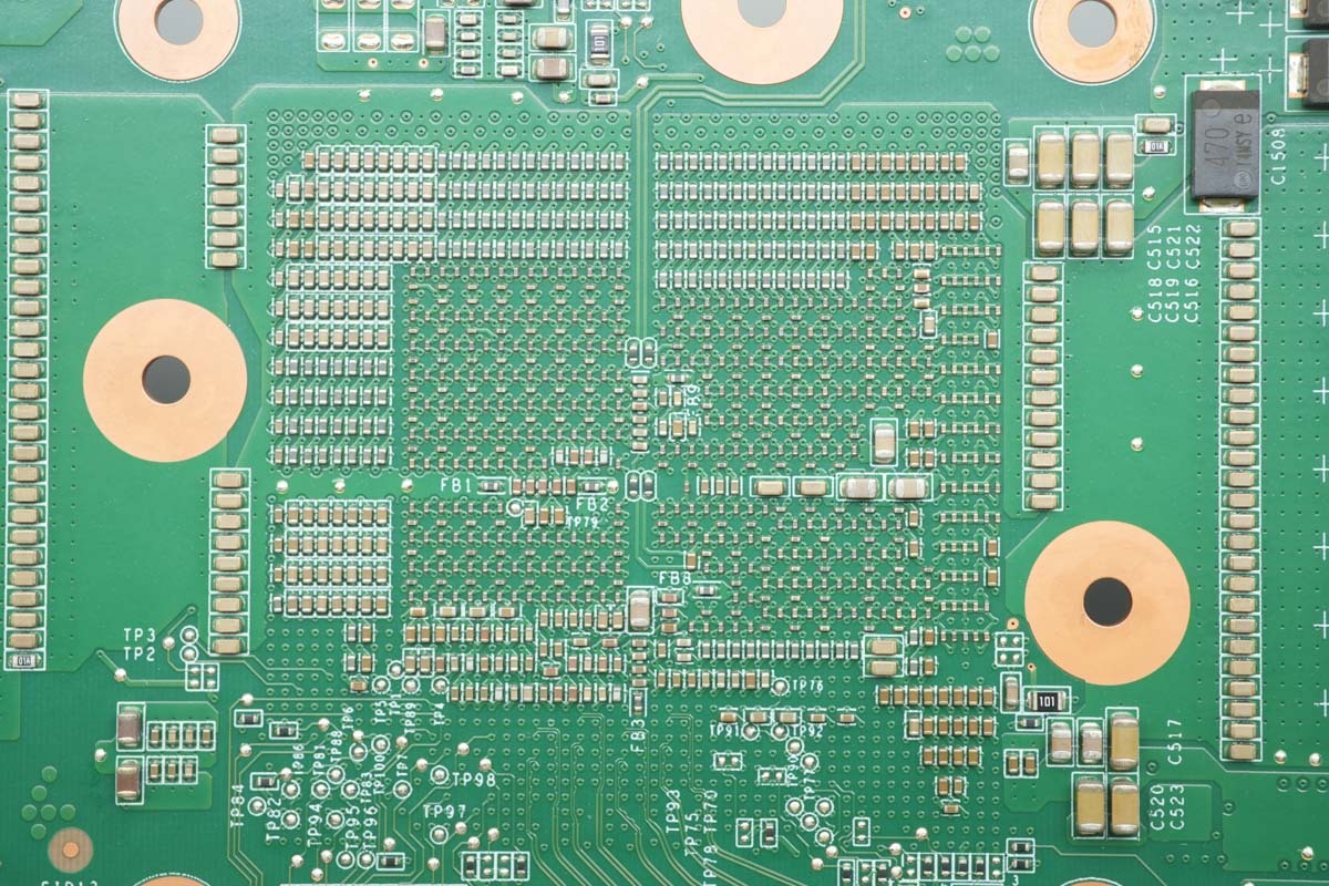
The back of the core is equipped with MLCCs for decoupling and filtering.
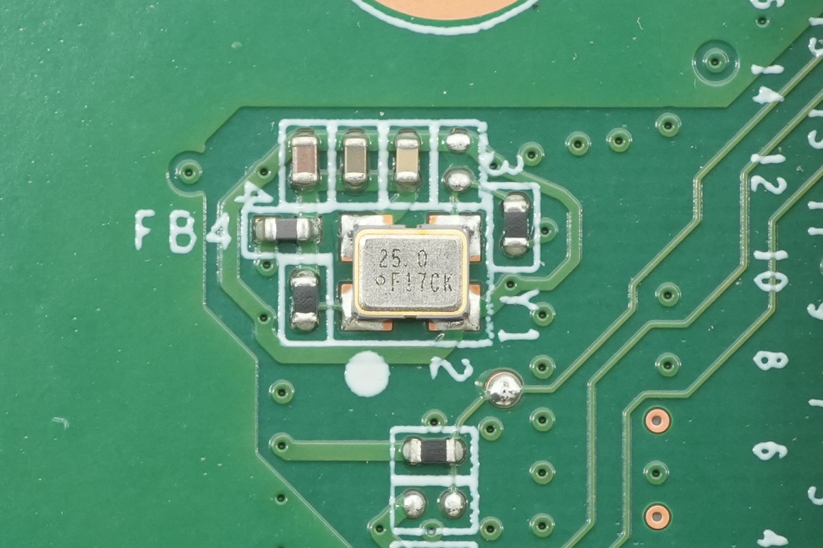
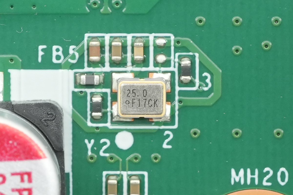
The chip features an external 25.000MHz crystal oscillator for clock reference.
The second 25.000MHz crystal oscillator.
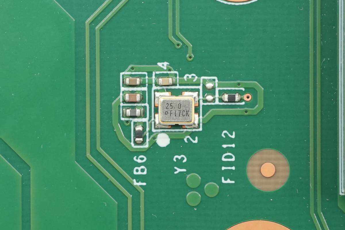
Three 25.000MHz crystal oscillators in total.
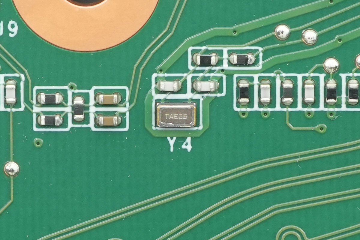
A 32.768kHz crystal oscillator.
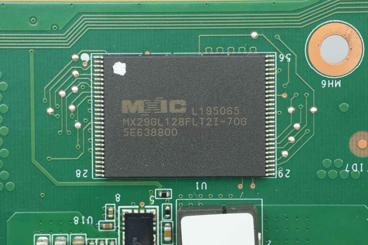
The memory chip is from MXIC, model number MX29GL128FLT2I-70G. It is a parallel NOR flash memory with a capacity of 16MB, supporting an operating voltage range of 2.7 to 3.6V, and is housed in a 56-pin TSOP.
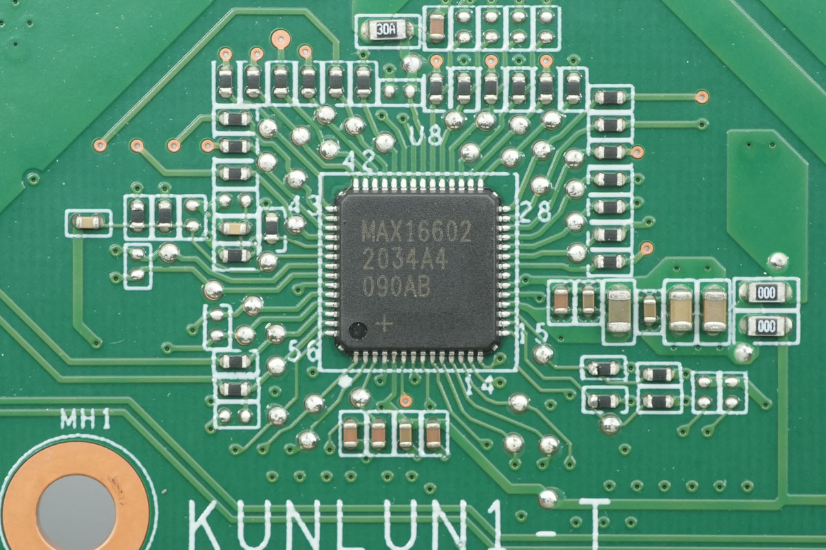
The multiphase step-deon controller is from ADI, model number MAX16602. It is a dual-output voltage regulator chipset for voltage regulator 13.HC+AI cores, supporting 8+1 phase synchronous buck conversion applications. It integrates an input power monitor, features a PMBus interface, supports digitally programmable configuration, and provides input voltage, current, and power monitoring. It is housed in a 56 QFN-EP.
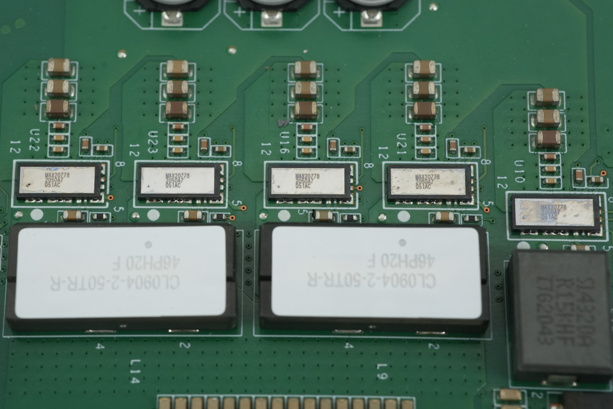
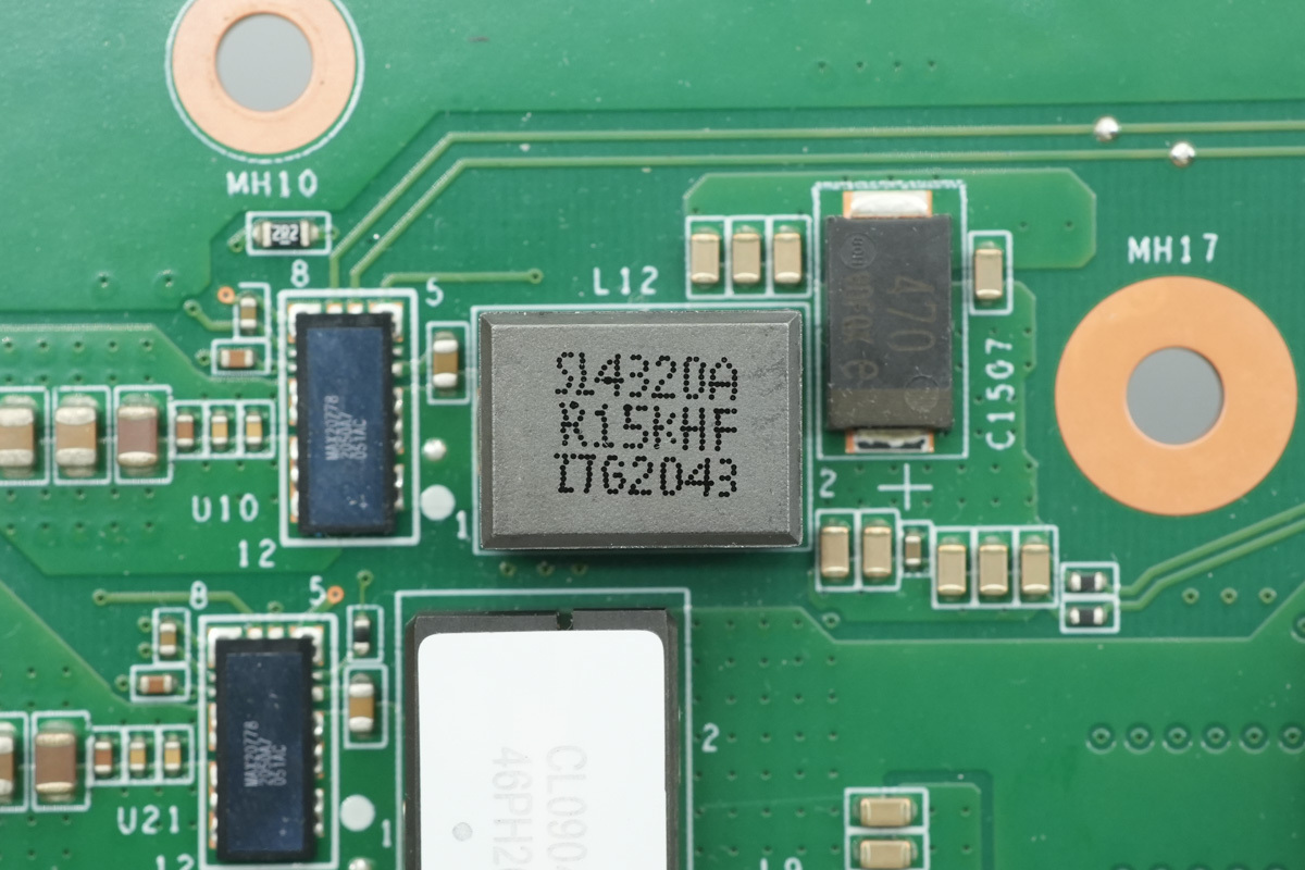
The smart power stage chip is from ADI, model number MAX20778. It integrates internal MOSFETs and is housed in a FCQFN package.
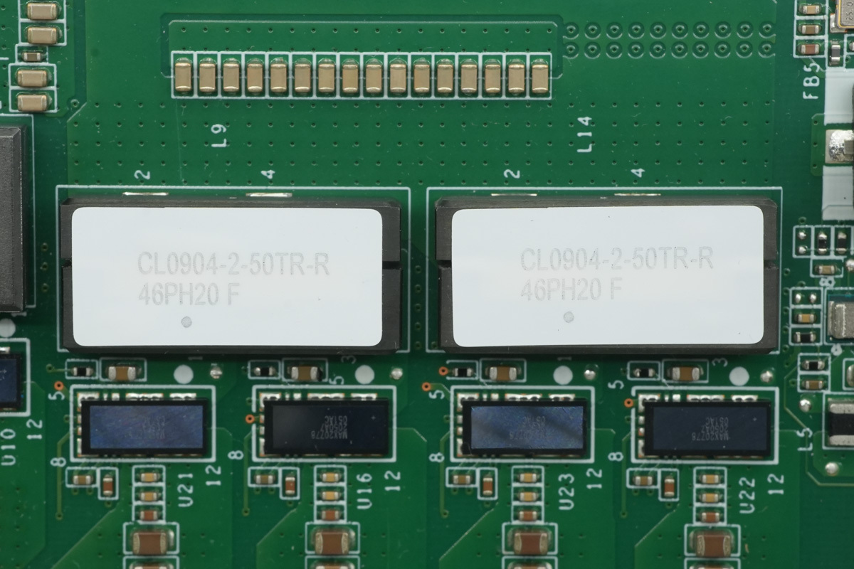
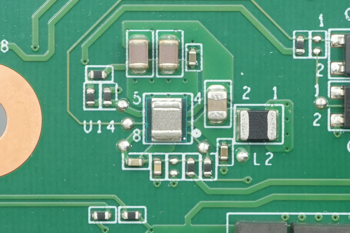
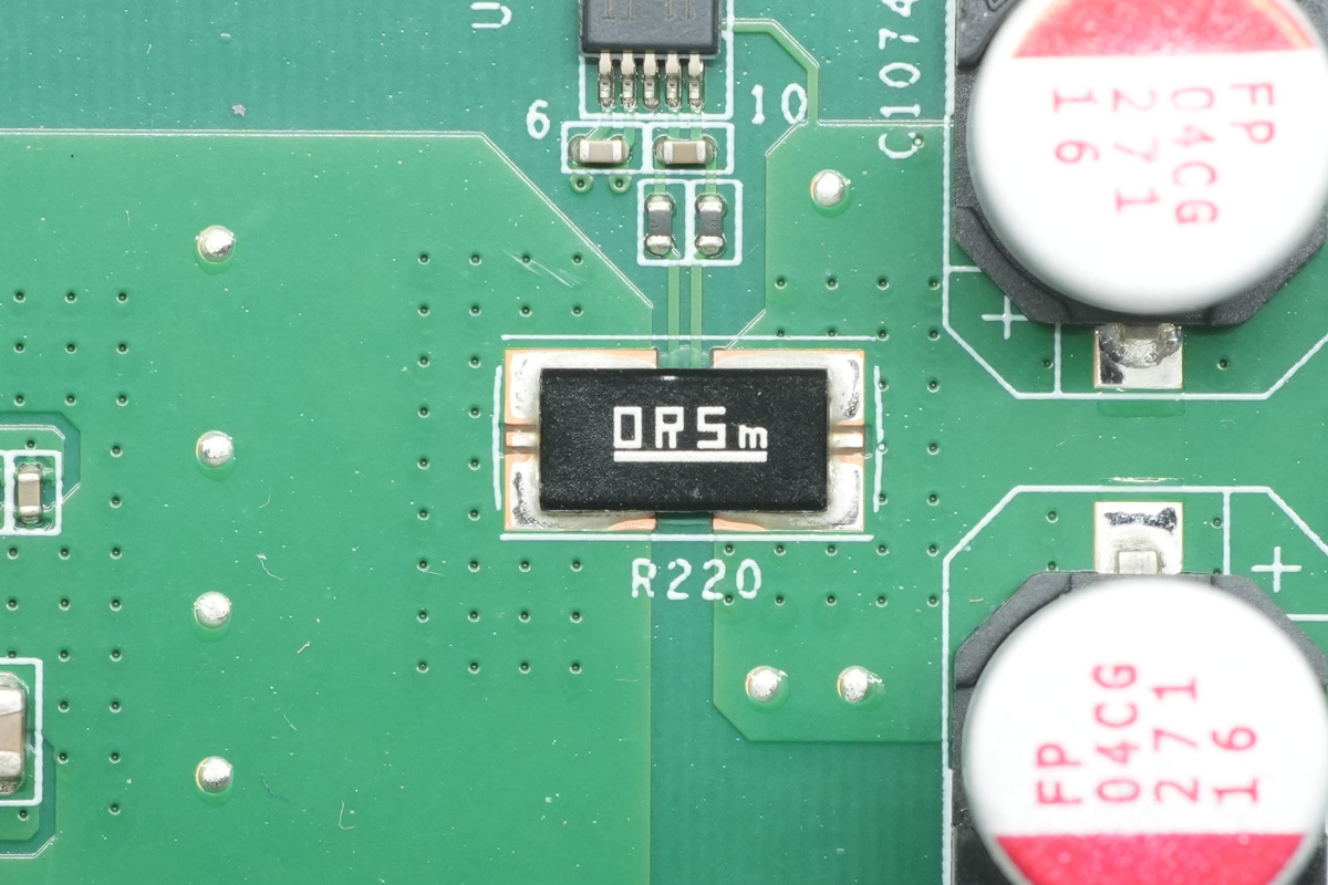
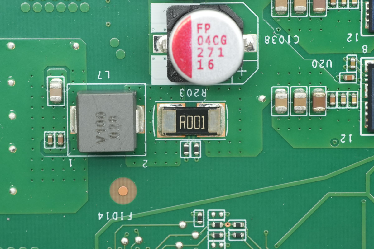
The step-down chokes are utilized for power delivery.
The step-down choke, 0.15μH.
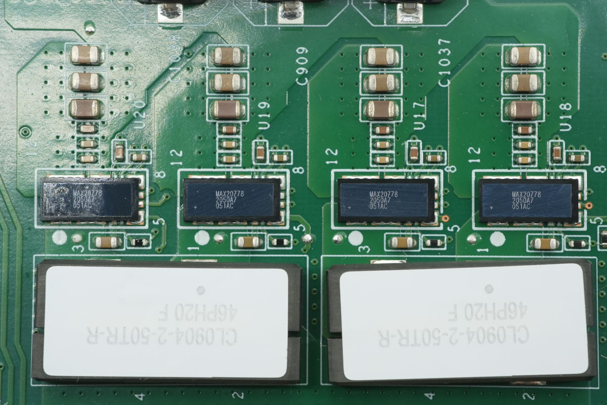
The smart power stage chip is from ADI, model MAX20778.
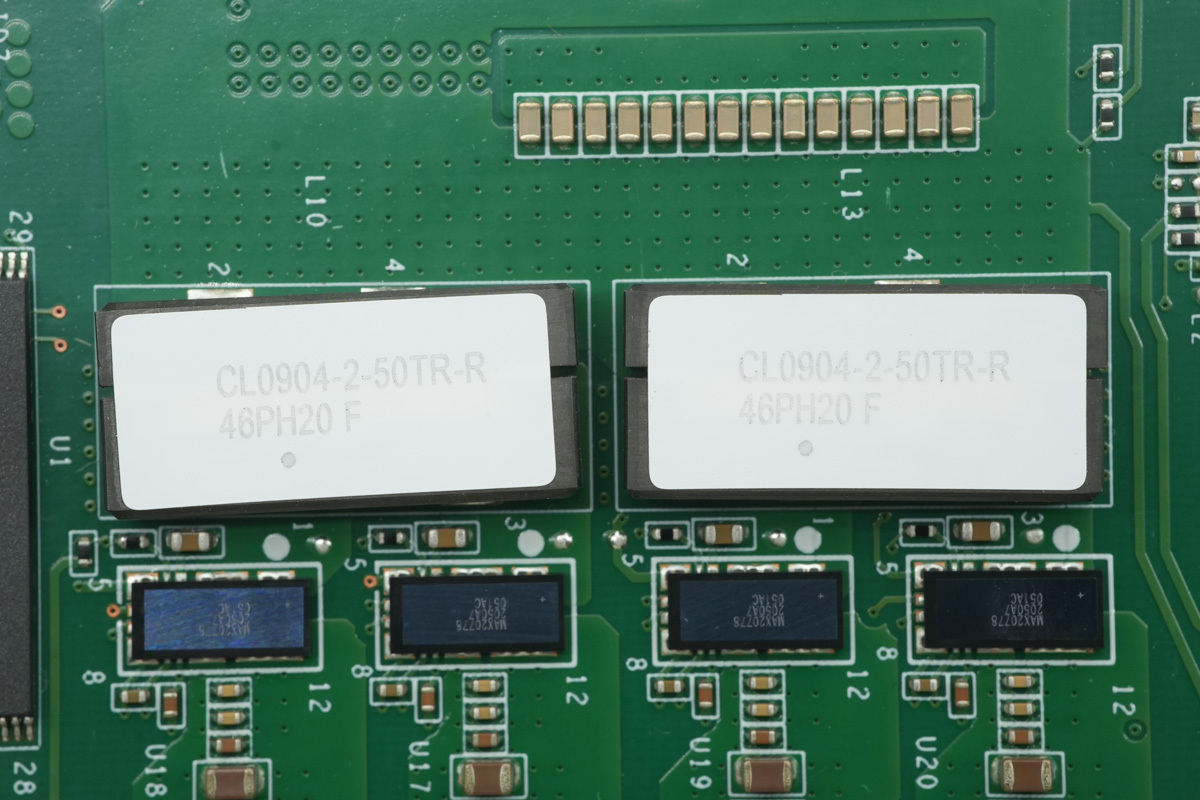
The step-down chokes are utilized for power delivery.
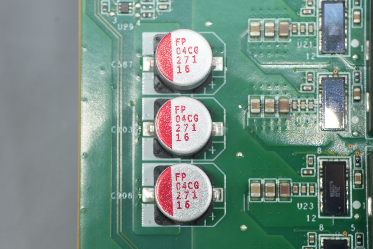
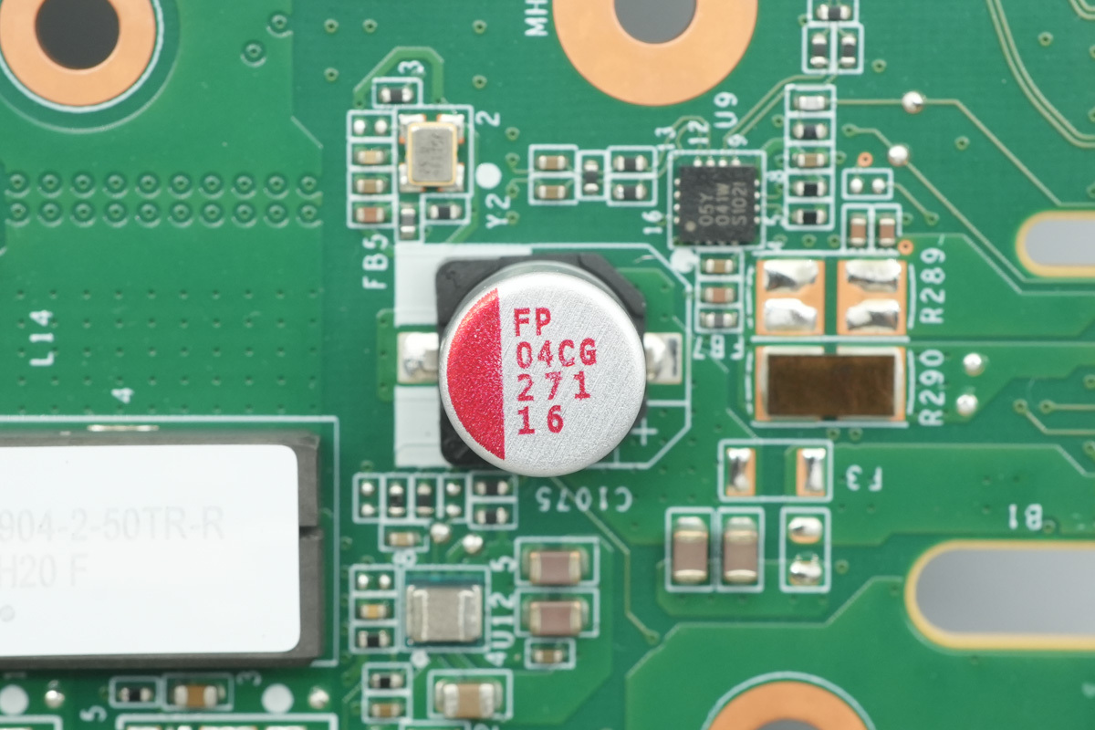
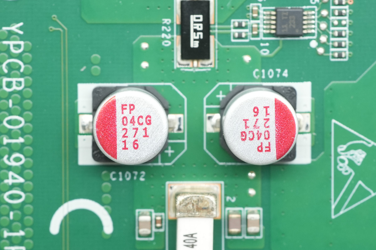
The three filtering caps are from Nichicon, spec 270μF16V.
Another one shares the same model.
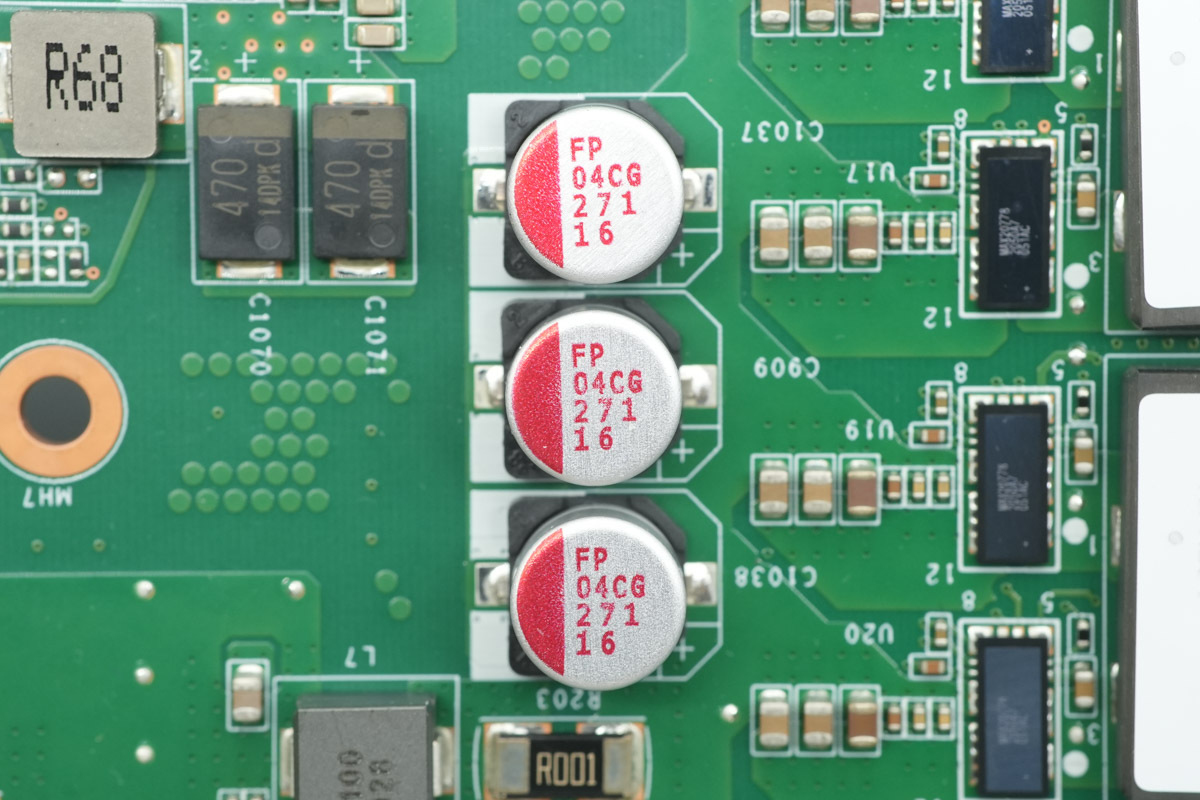
Three filtering caps of the same model are located on the right side.
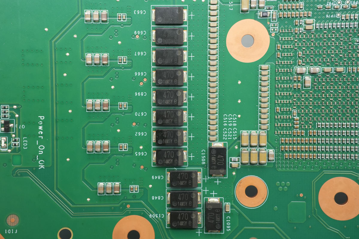
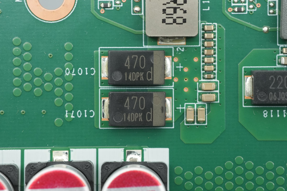
The back of the PCBA is equipped with 13 SMD filtering caps from the Panasonic SP-CAP series, spec 470μF2.5V.
The front side features another filtering cap of the same model.

8 filtering caps of the same model are provided on the other side.
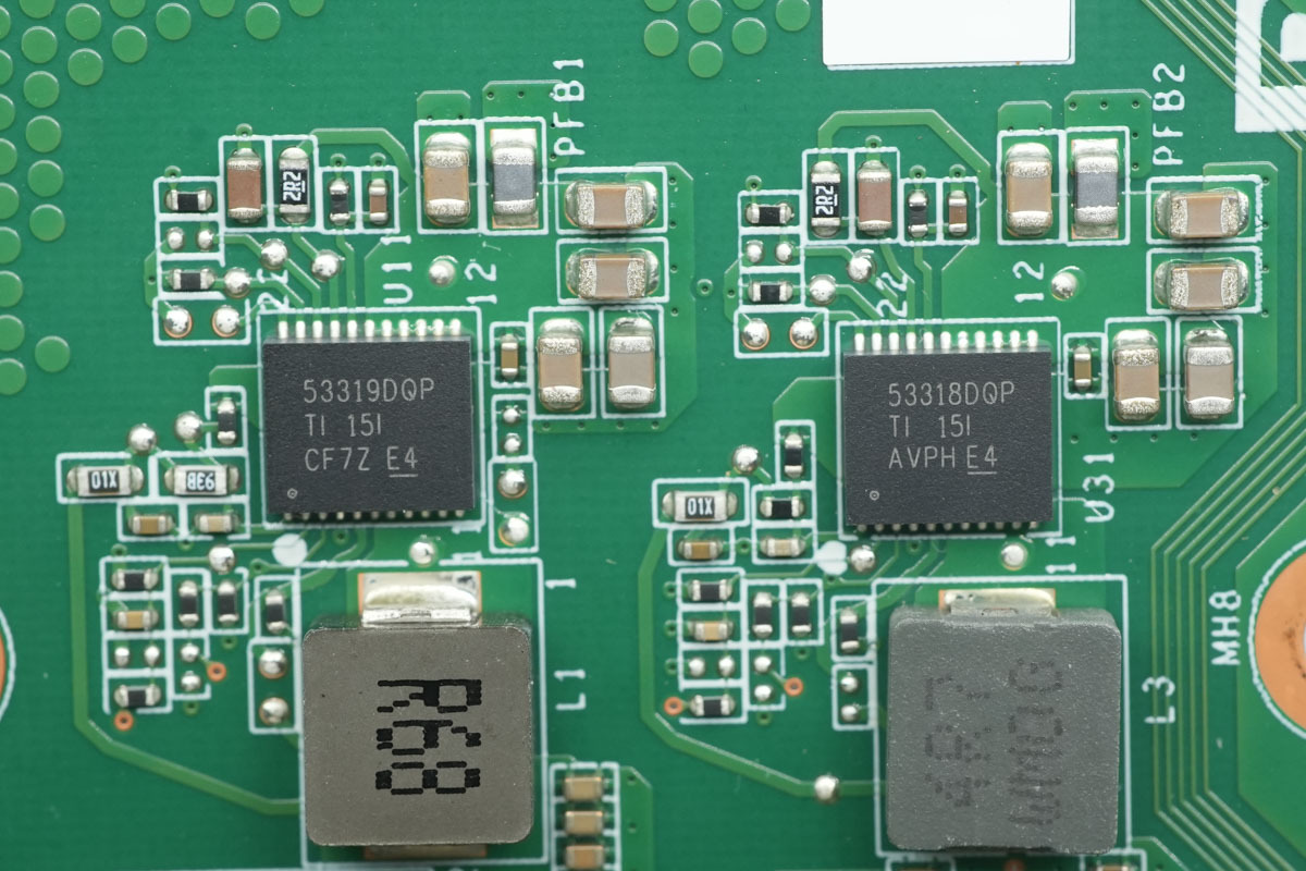
Two synchronous step-down chips are from TI, model TPS53319 and TPS51138, respectively. These are synchronous step-down converters with Eco-mode control, supporting an input voltage range of 1.5-22V and an output voltage range of 0.6-5.5V. They feature a 5V low-dropout regulator output and D-CAP ultra-fast transient control, and are housed in a QFN22 package. The TPS53319 supports an output current of 14A, while the TPS51138 supports an output current of 8A.
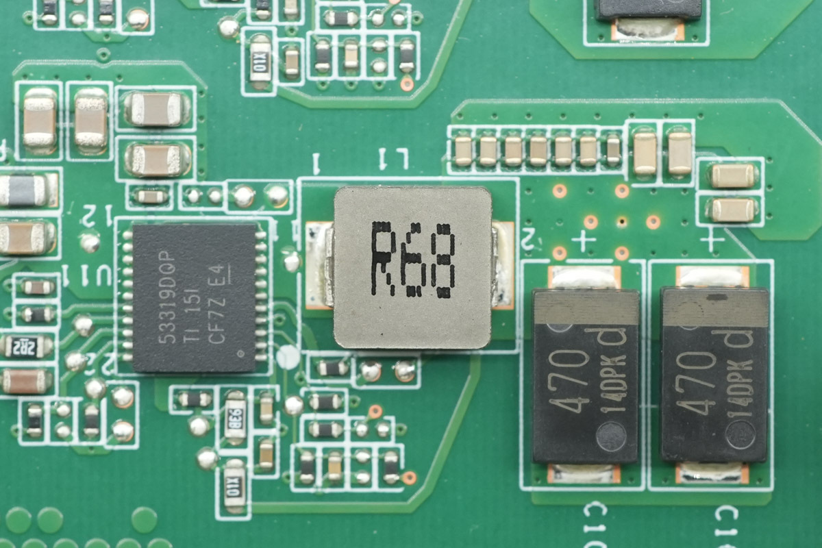
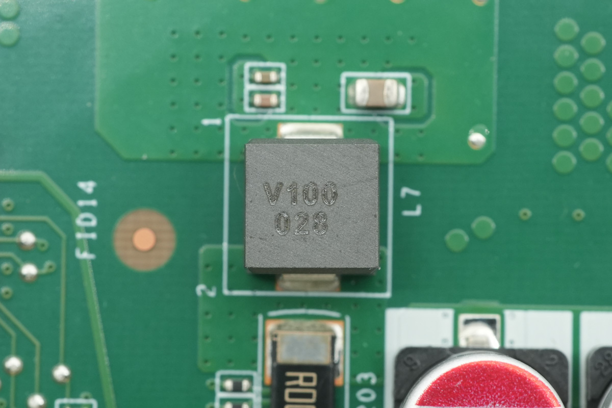
The TPS53319 is used with a 0.68μH step-down choke.
The two filtering caps, 470μF 2V.
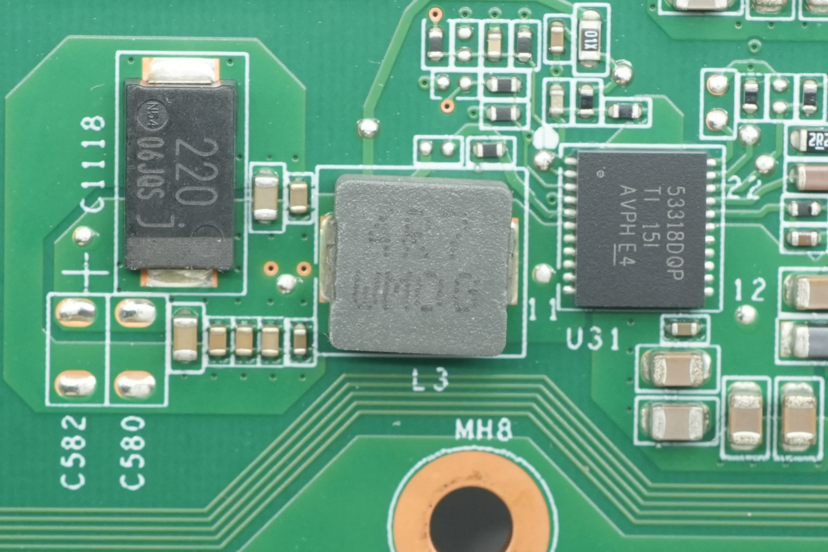
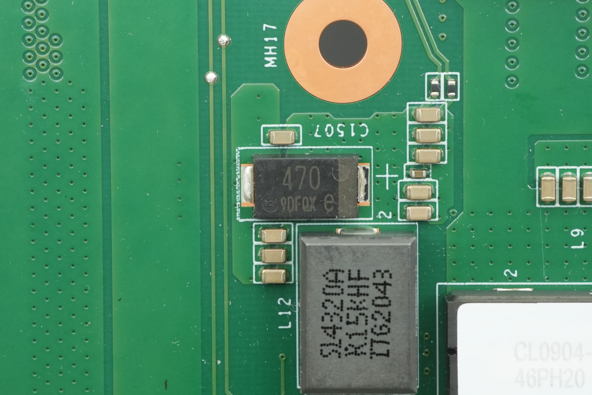
The TPS53318 is paired with a 4.7μH step-down choke.
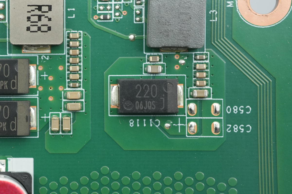
The filter cap, 220μF 6.3V.
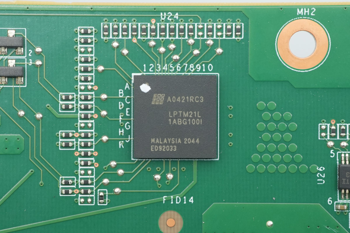
The hardware management controller is from LATTICE, belongs to the Lattice Platform Manager 2 series, model number LPTM21L-1ABG100I. It is a programmable logic-based, fast-response hardware management controller that integrates analog sensors, control components, and programmable logic resources. It supports power management, thermal management, and control functions, and is housed in a 100-ball caBGA package.
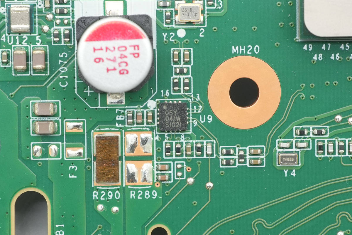
A chip, marked 05Y 041W S102I.
The power conversion module is from TI, and in a uSIP8 package.
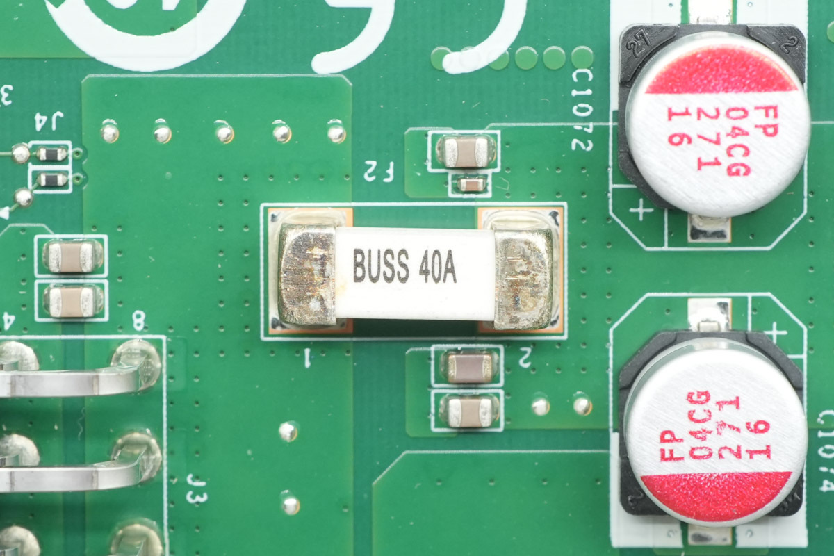
The input fuse, 40A.
The two filtering caps are from Nichicon, spec 270μF16V.
A 0.5 mΩ current sense resistor is utilized for input current detection.
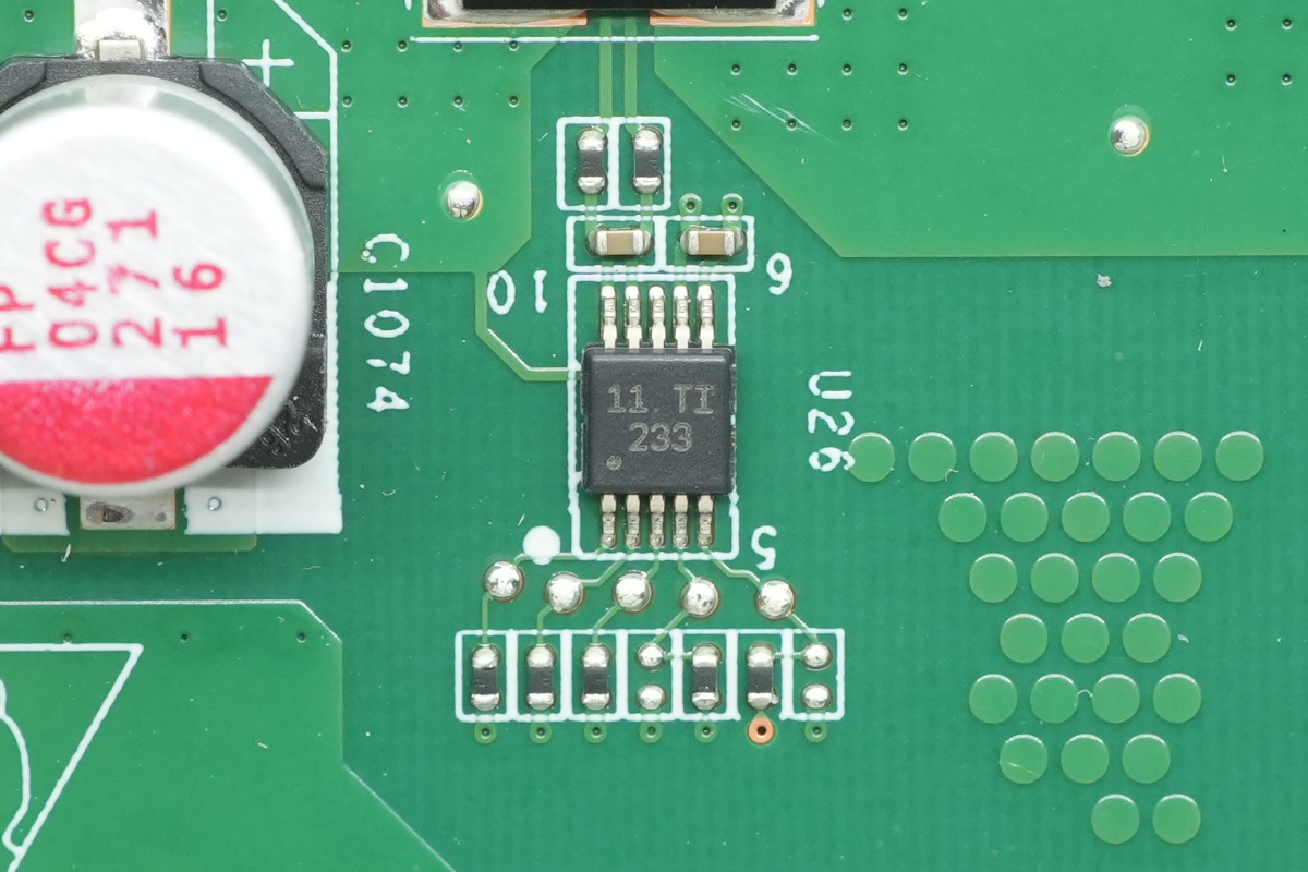
The power monitoring chip is from TI, model INA233. It is a 36V bus voltage, 16-bit voltage, current, and power monitor chip that features I2C, SMBus, and PMBus interfaces. The device supports high-side or low-side sensing, features 16 programmable addresses, and is housed in a VSSOP10 package.
The SMD filtering choke.
A 1mΩ current sense resistor is utilized for input current detection.
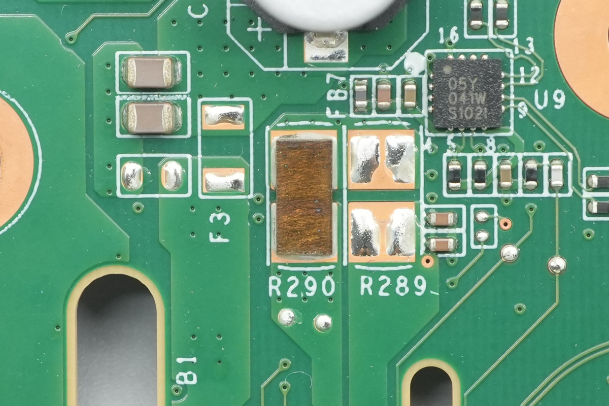
This is a SMD current sense resistor.
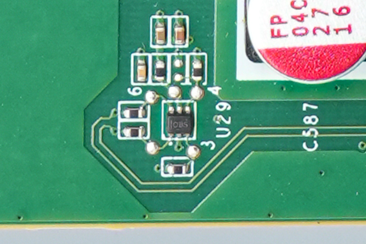
The temperature sensor is from TI, marked OBS, model TMP112A. It is a high-accuracy, low-power digital temperature sensor featuring SMBus and two-wire serial interfaces, and is housed in a SOT563 package.
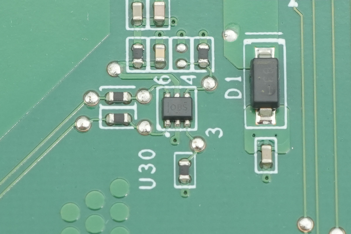
Another one shares the same model.
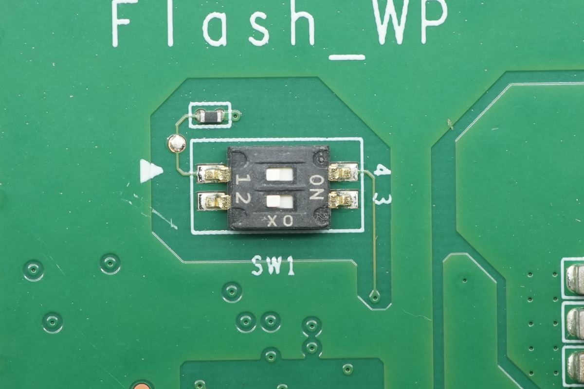
A DIP switch is soldered onto the back of the PCBA.
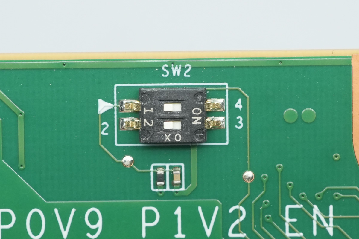
Another DIP switch.
Well, those are all components of Baidu Kunlunxin AI Accelerator Card K200.
Summary of ChargerLAB
The Baidu Kunlunxin K200 AI accelerator card pairs a 1-Gen Kunlunxin chip with a dual-slot, full-length/full-height design. Featuring PCIe Gen4*8 support, the card is encased in a black aluminum alloy shell that utilizes system airflow to cool an integrated pass-through passive heat sink. Built on the 14nm XPU-K architecture, it also includes 16GB of HBM memory.
Teardown confirms the KUNLUN1-T core utilizes a dedicated heat pipe radiator. Power management relies on ADI components, utilizing a MAX16602 and MAX20778 combination for an 8+1 phase configuration, with thermal pads ensuring efficient heat dissipation via the frame.
Rounding out the specs are TI converters (TPS53319 and TPS53318), an INA233 power monitor, and a TMP112A temperature sensor. High-quality filtering is provided by Nichicon solid caps and Panasonic SP-CAPs, reflecting a reliable and well-engineered design.
Related Articles:
1. Teardown of CUKTECH 10 Super Magnetic Power Card (WPB100P)
2. BPS Launches BPD93136, BPD93204, and BPD80350E DrMOS for NVIDIA Graphics Cards and High-Performance Power Management
3. Mingfan Releases New External Graphics Card with Built-in 240W GaN Power Supply and OCuLink Interface Support