Introduction
In recent years, the addition of power display features has become an important way to distinguish between new and older models of chargers. By showing power usage directly on the charger, users can intuitively understand the device's power consumption. SHARGE has launched a GaN charger equipped with a pixel dot-matrix display. The charger features three USB-C ports, each supporting 140W fast charging. The pixel dot-matrix display can show both the active charging port and the real-time charging power. It also includes a button for adjusting display brightness and orientation. Let’s take it apart to see its internal components and structure.
Product Appearance
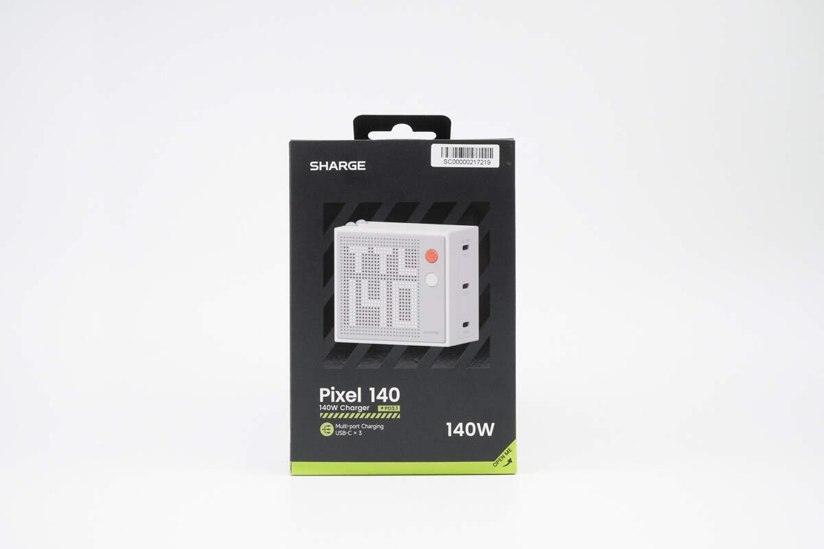
The front of the packaging box features the SHARGE logo, an image of the product, as well as the text "Pixel 140W" and "140W".
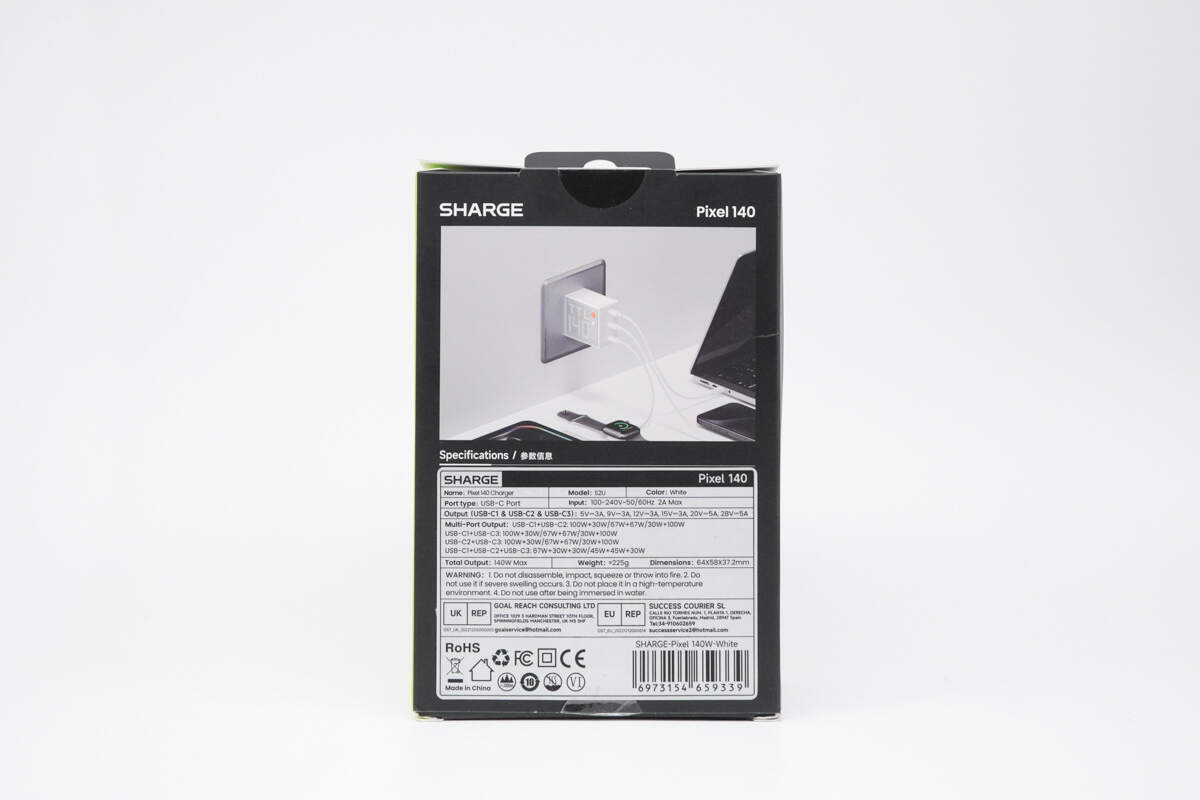
The back of the packaging displays usage scenarios and spec info.
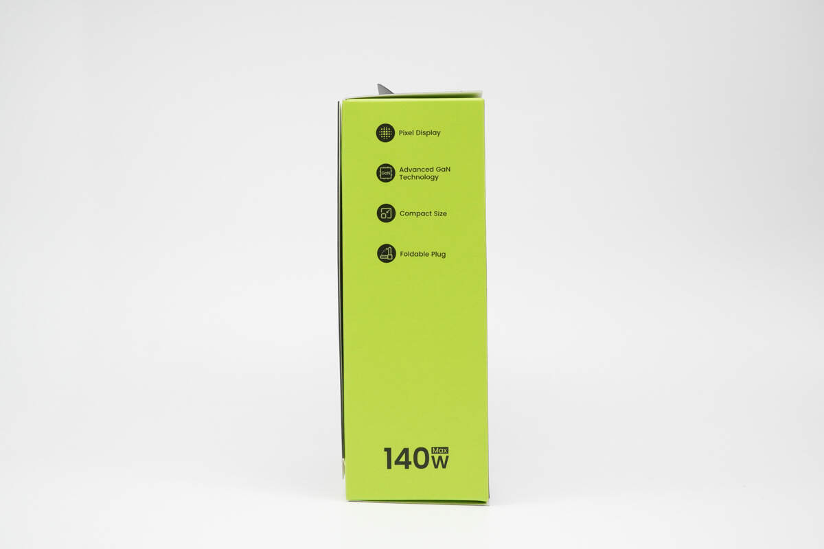
The sides highlight the selling points.

The other side indicates that the product is available in two color options.
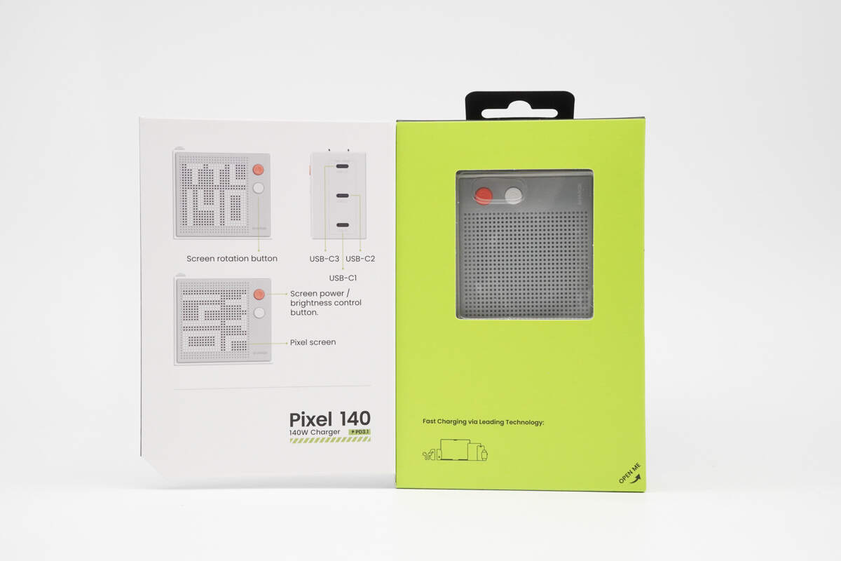
Upon opening the packaging, the charger is secured in a blister pack, with button usage instructions printed inside.
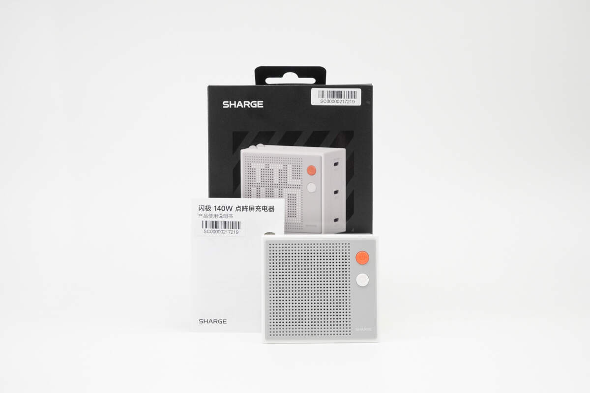
The packaging contains the charger and some documents.
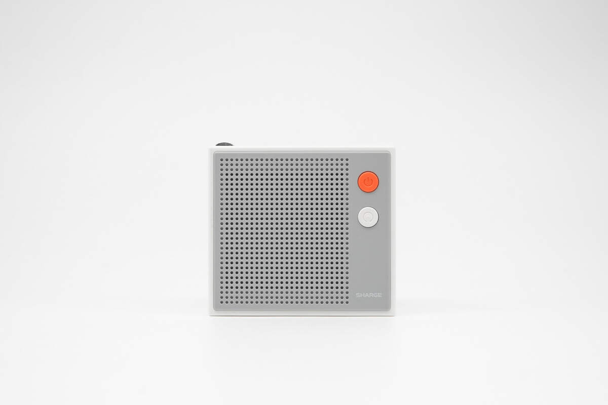
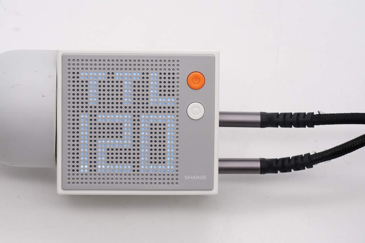
This side features the dot-matrix display and two buttons.
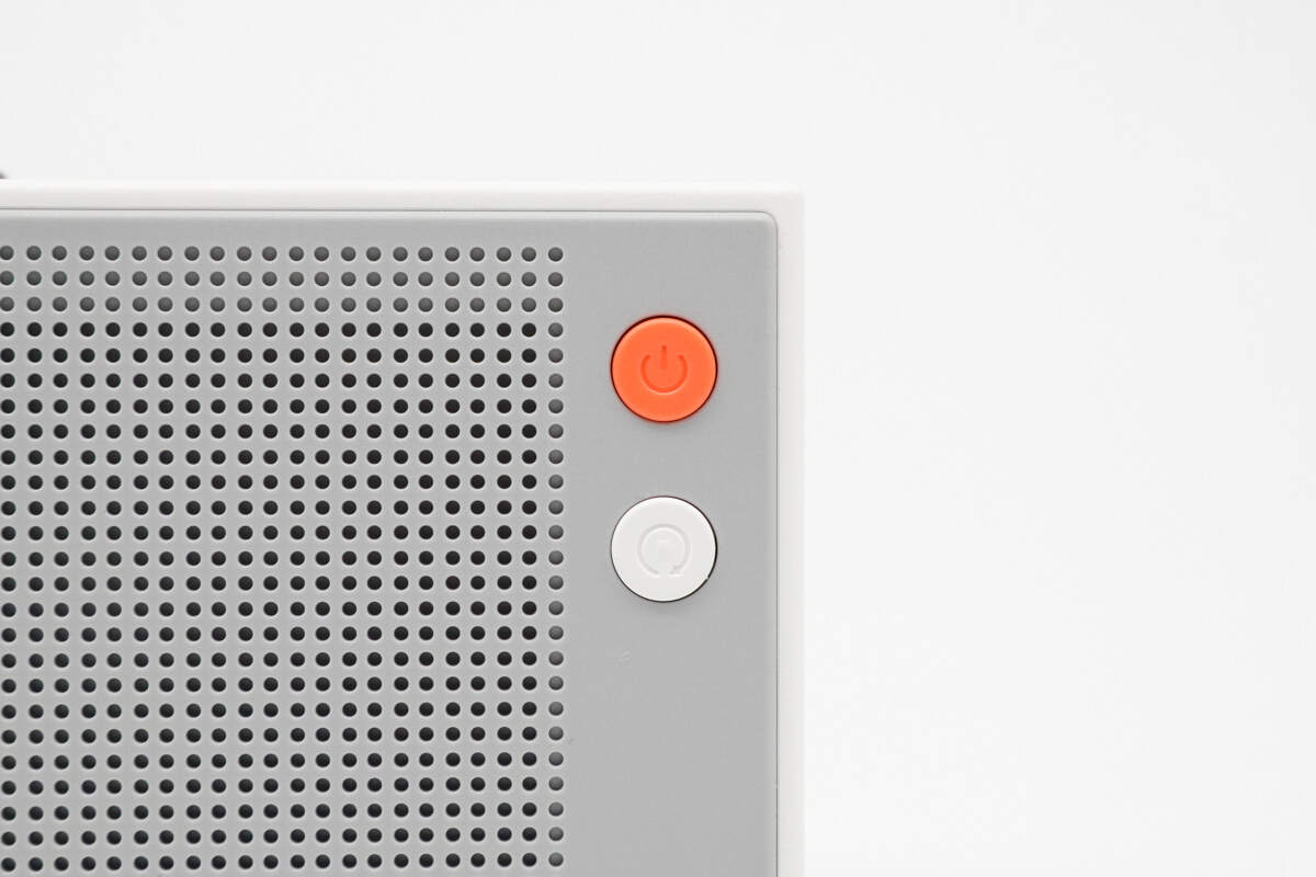
The orange button serves as the power switch, while the white button is used to control the display.
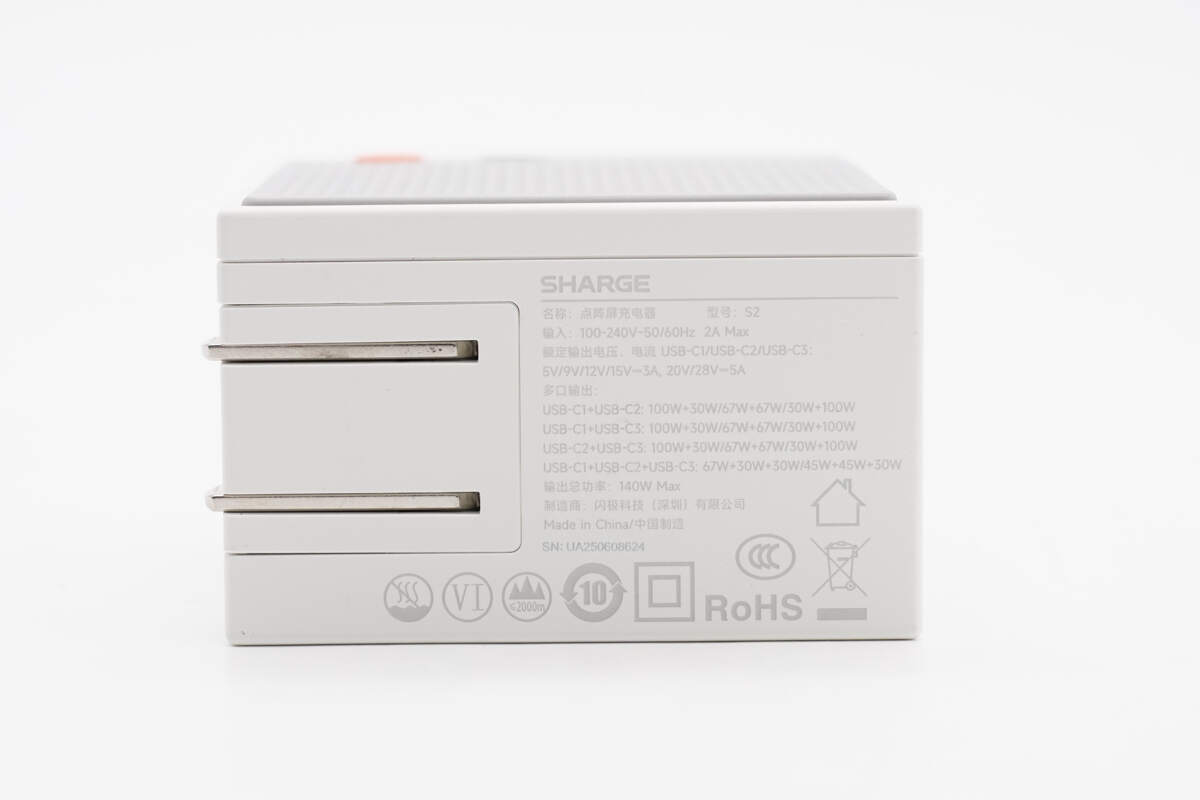
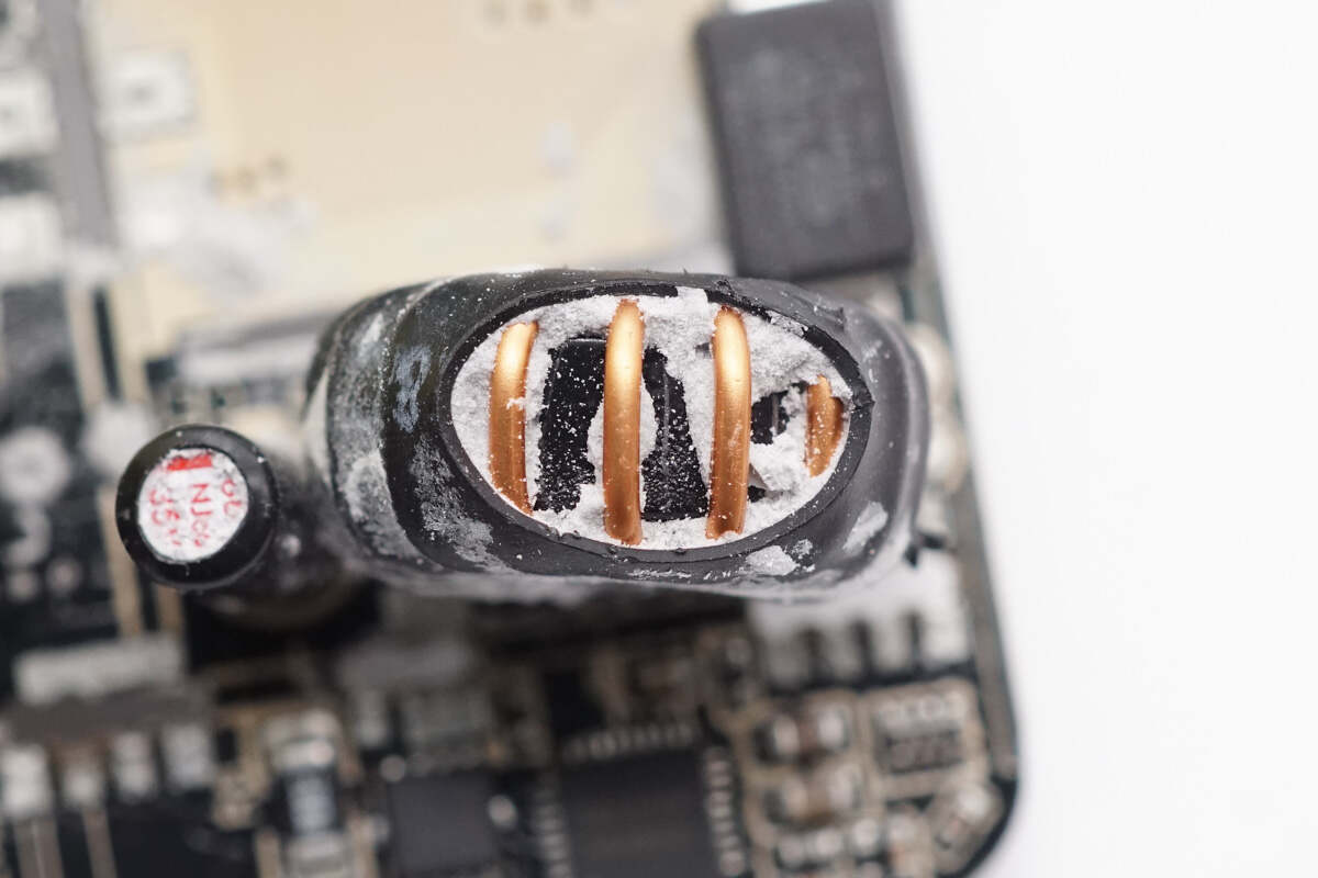
It comes with foldable prongs, and the input end casing is printed with spec info.
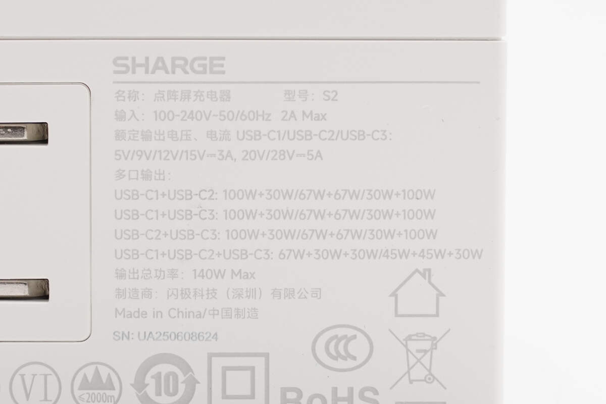
Model: S2
Input: 100-240V\~50/60Hz 2A Max
Rated Output Voltage/Current USB-C1/USB-C2/USB-C3:
5V/9V/12V/15V 3A, 20/28V 5A
Multiple Port Output:
USB-C1 + USB-C2: 100W + 30W / 67W + 67W / 30W + 100W
USB-C1 + USB-C3: 100W + 30W / 67W + 67W / 30W + 100W
USB-C2 + USB-C3: 100W + 30W / 67W + 67W / 30W + 100W
USB-C1 + USB-C2 + USB-C3: 67W + 30W + 30W / 45W + 45W + 30W
Total Output Power: 140W Max
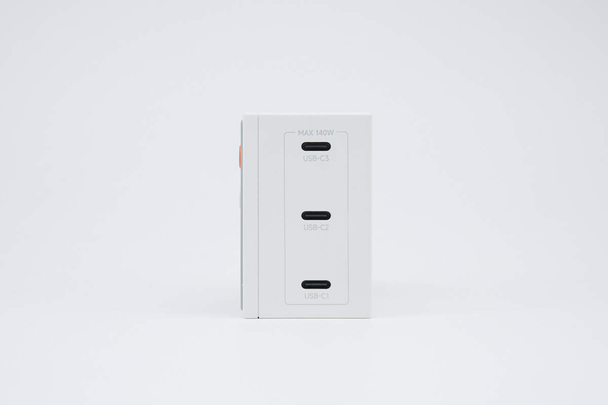
The output end is equipped with three USB-C ports.
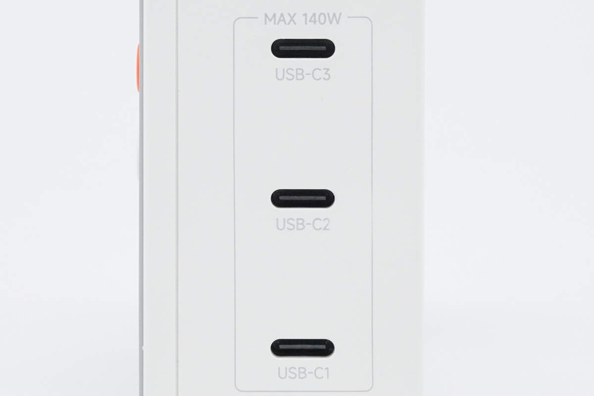
The ports are labeled with a maximum output power of 140W.
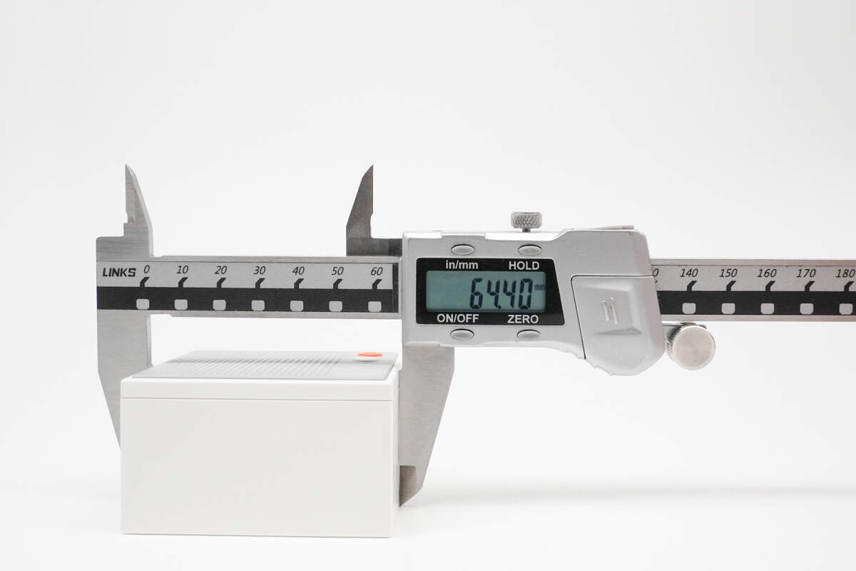
The length of the charger is about 64.4 mm (2.54 inches).
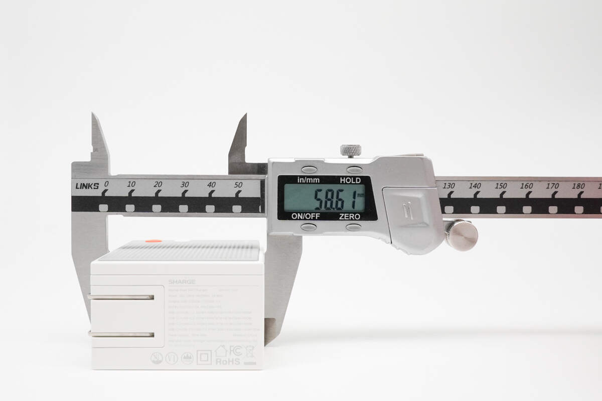
The width is about 58.6 mm (2.31 inches).
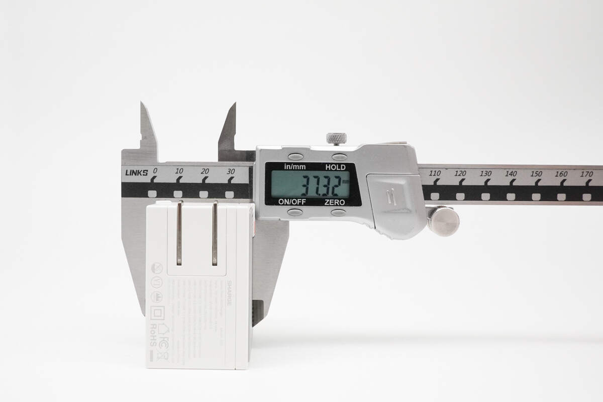
The thickness is about 37.3 mm (1.47 inches).
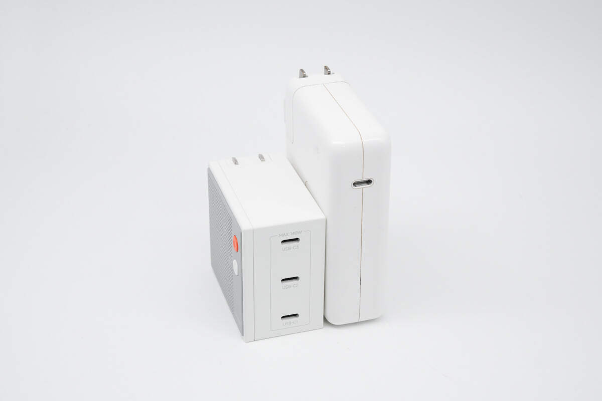
It is much smaller than the Apple 140W charger.

That's how big it is in the hand.
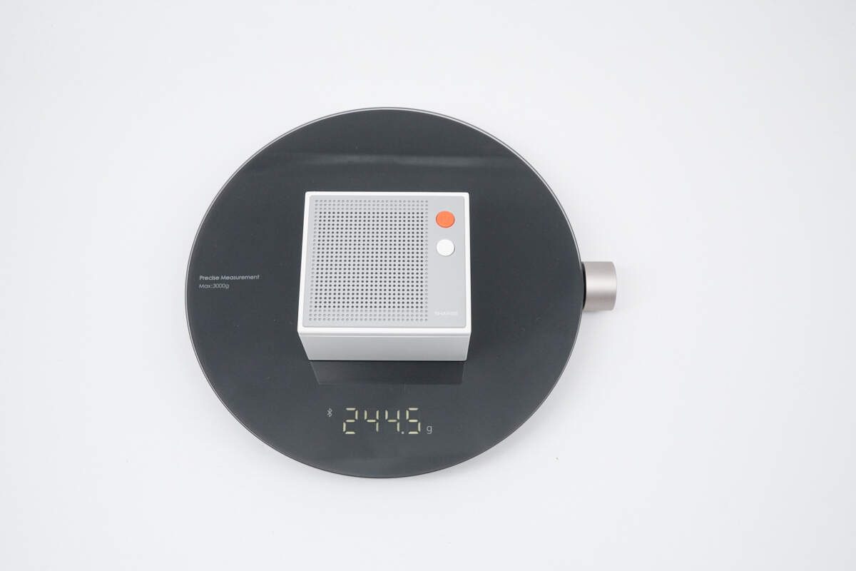
The weight is about 244.5 g (8.62 oz).
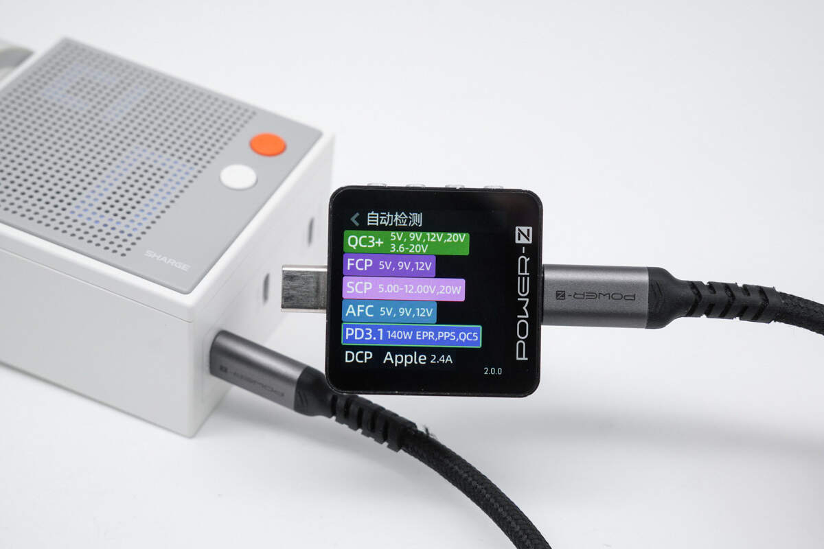
ChargerLAB POWER-Z KM003C shows that the USB-C1/C2/C3 supports FCP, SCP, AFC, PD3.1, PPS, QC3+/5, DCP, and Apple 2.4A protocols.
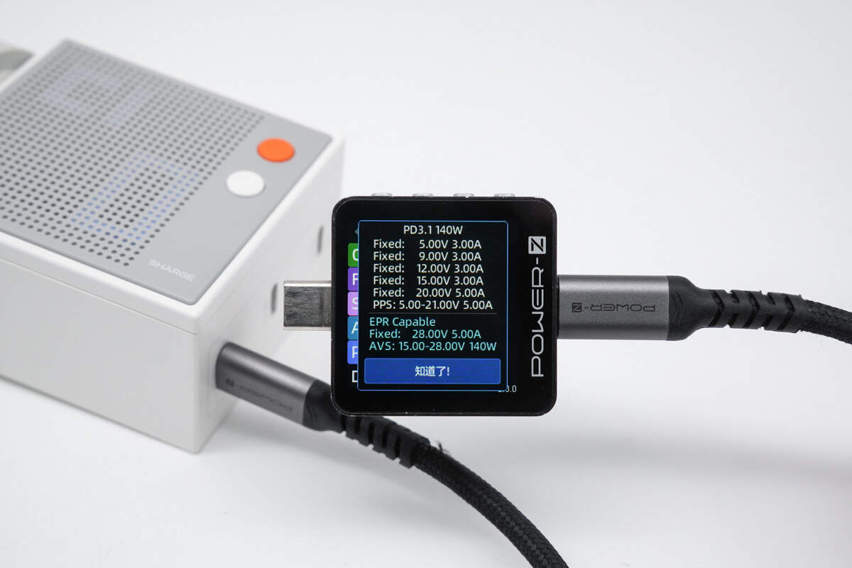
It supports six fixed PDOs of 5V3A, 9V3A, 12V3A, 15V3A, 20V5A, and 28V5A. It also supports one set of PPS (5–21V, 5A) and one set of AVS (15–28V, 140W).
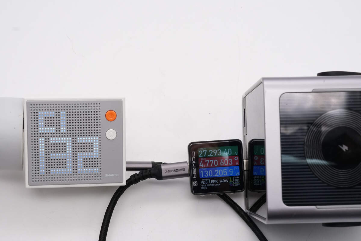
Use it to charge the CUKTECH 30 power bank, the power is about 132W.
When multiple ports are used simultaneously, the display shows the total output power. "TTL" is the abbreviation for "Total".
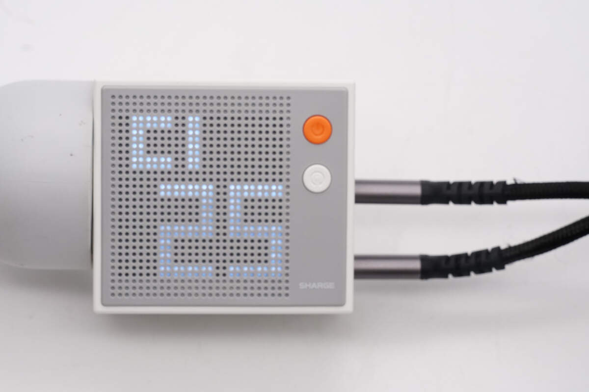
The dot-matrix display shows that the USB-C1 is outputting 25W of power.
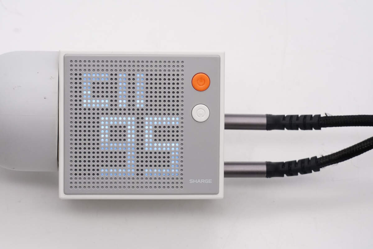
The dot-matrix display shows that the USB-C2 is outputting 95W of power.
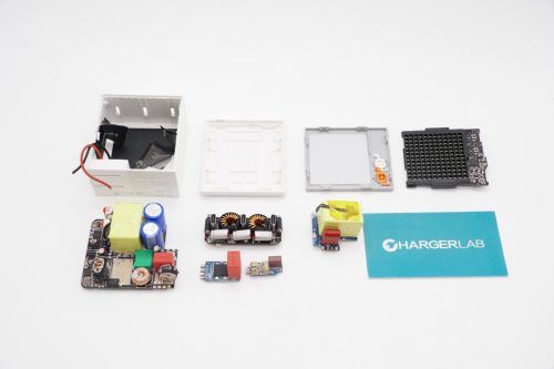
Teardown
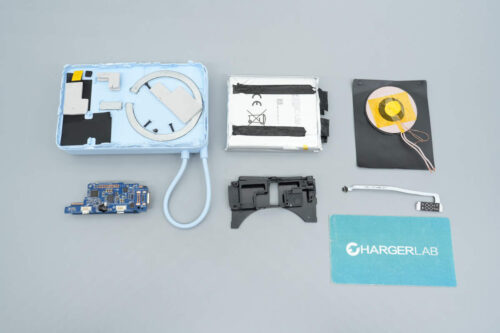
Next, let's take it apart to see its internal components and structure.
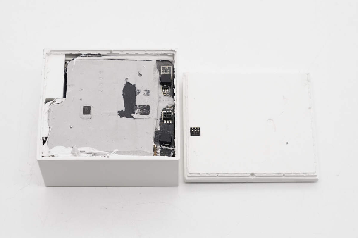
Pry open the dot matrix display module along the gap; the housing is fixed by ultrasonic welding.
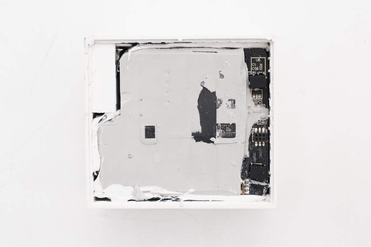
The PCBA module is filled with potting compound to improve heat dissipation and weather resistance.
The dot matrix display module is connected to the PCBA module via pin headers.
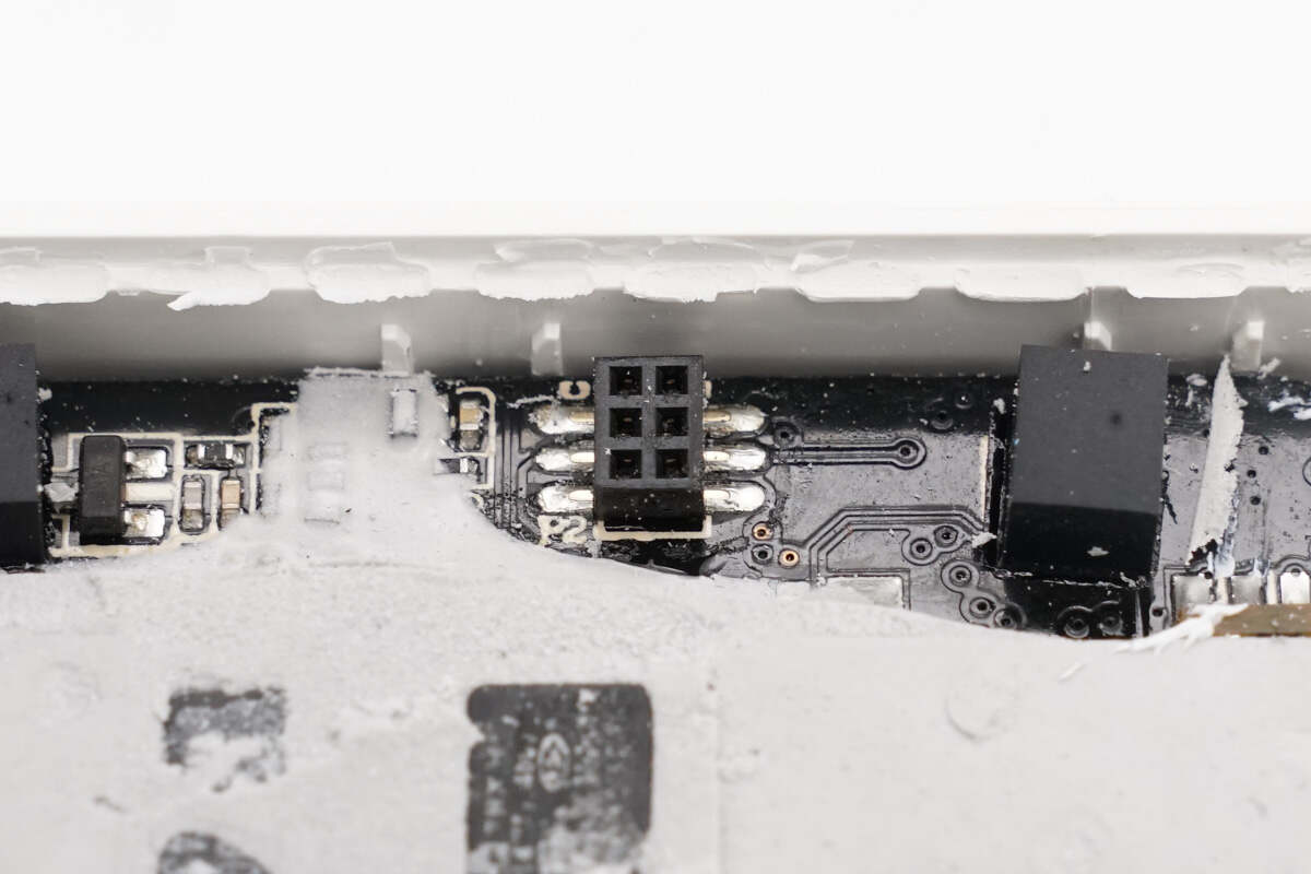
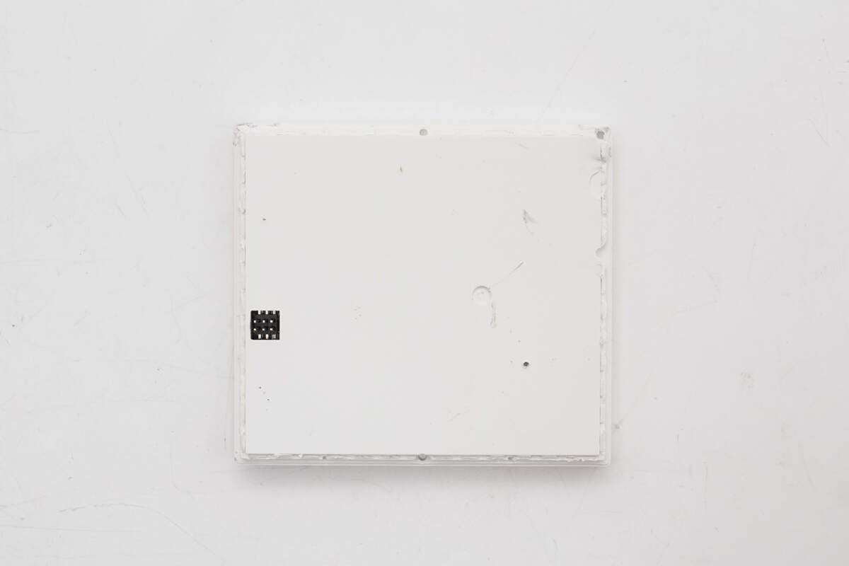
The PCBA module is equipped with the socket.
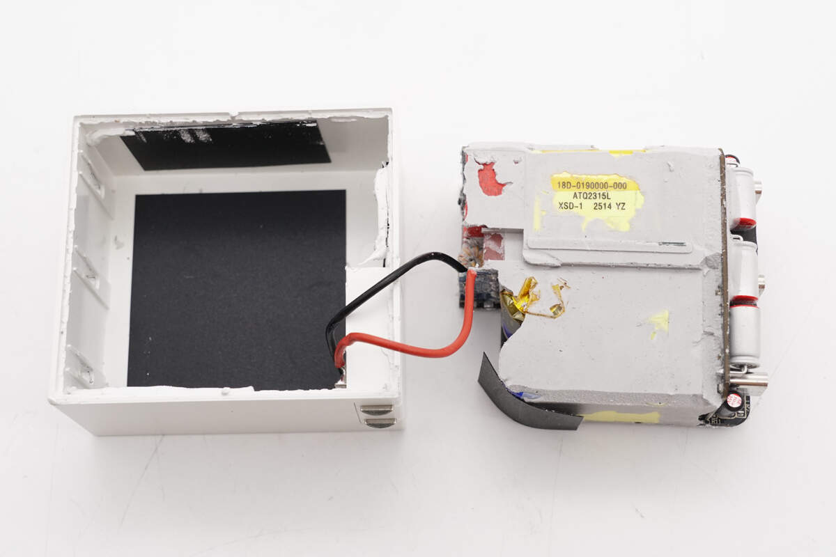
The foldable pins are connected to the PCBA module via wires, and graphite thermal conductive stickers are attached inside the housing.
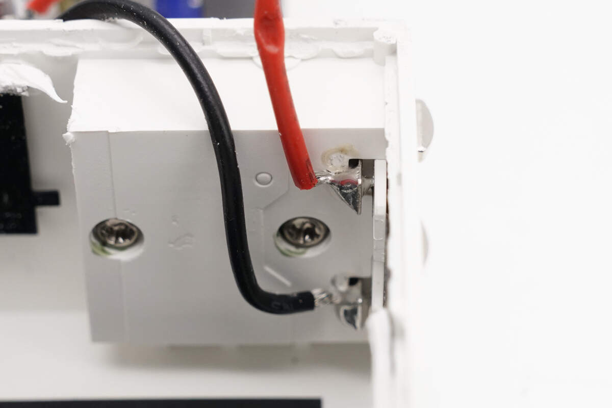
The wires are soldered to the pins.
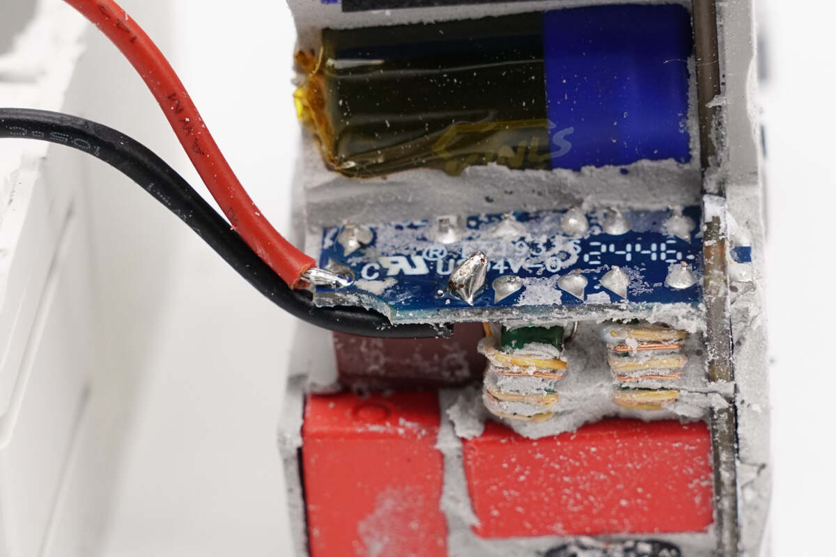
The other end is soldered to the PCBA module.
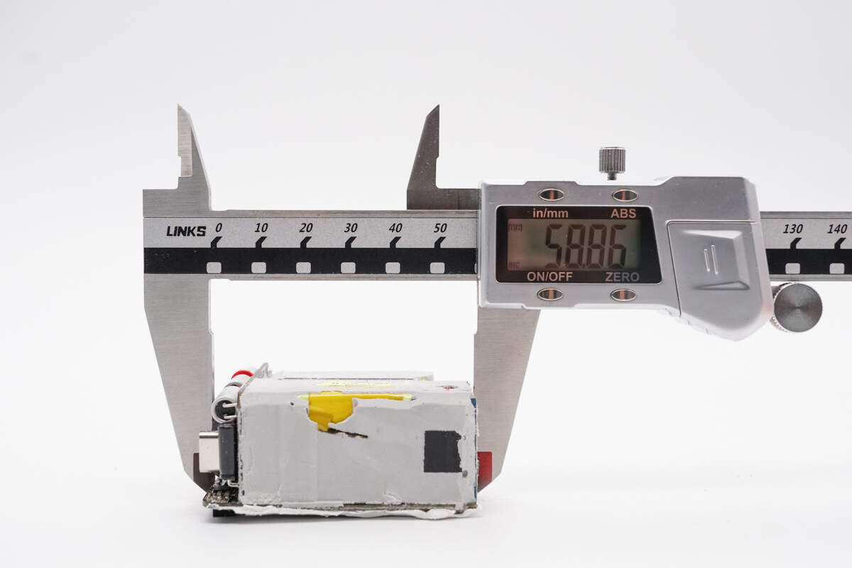
The length of the PCBA module is about 58.9 mm (2.32 inches).
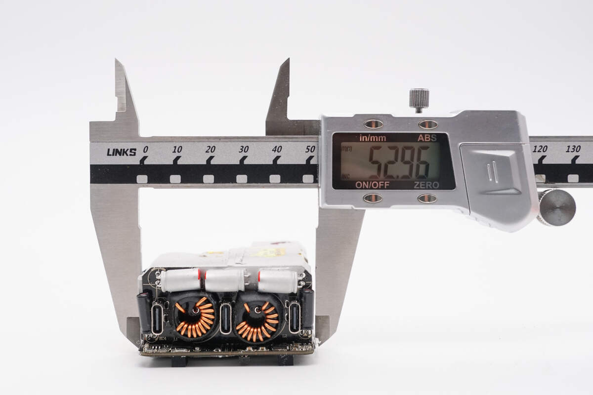
The width is about 53 mm (2.087 inches).
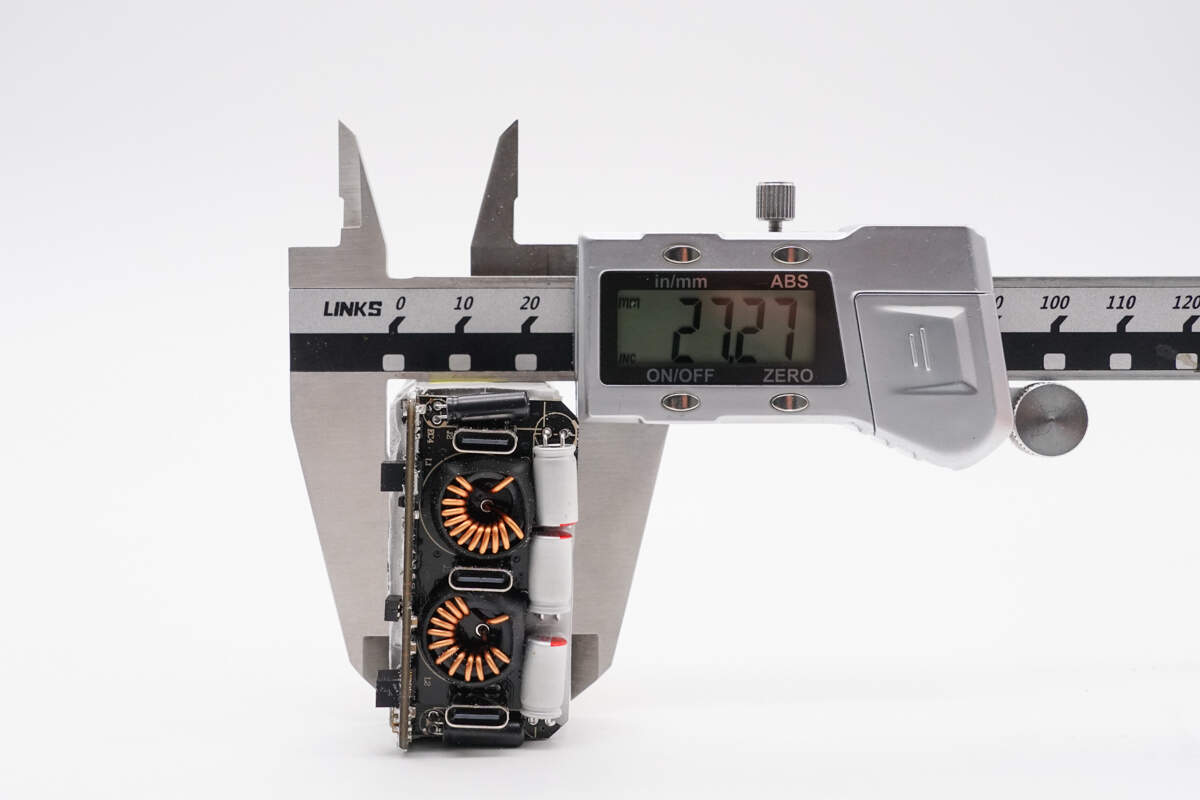
The thickness is about 27.3 mm (1.075 inches).
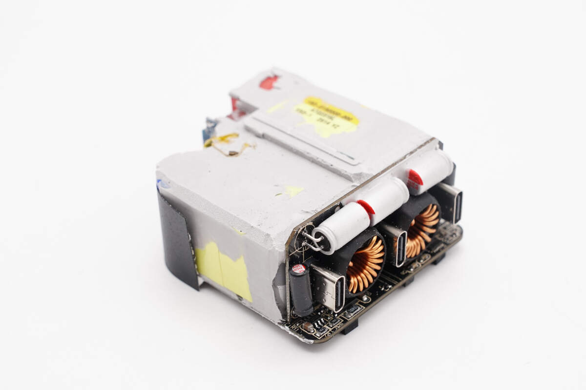
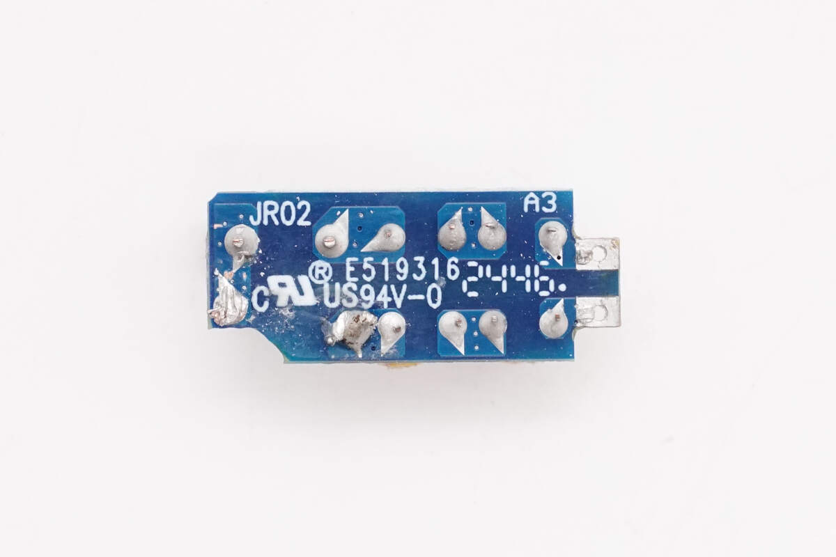
The PCBA module is assembled by soldering together multiple small PCBs.
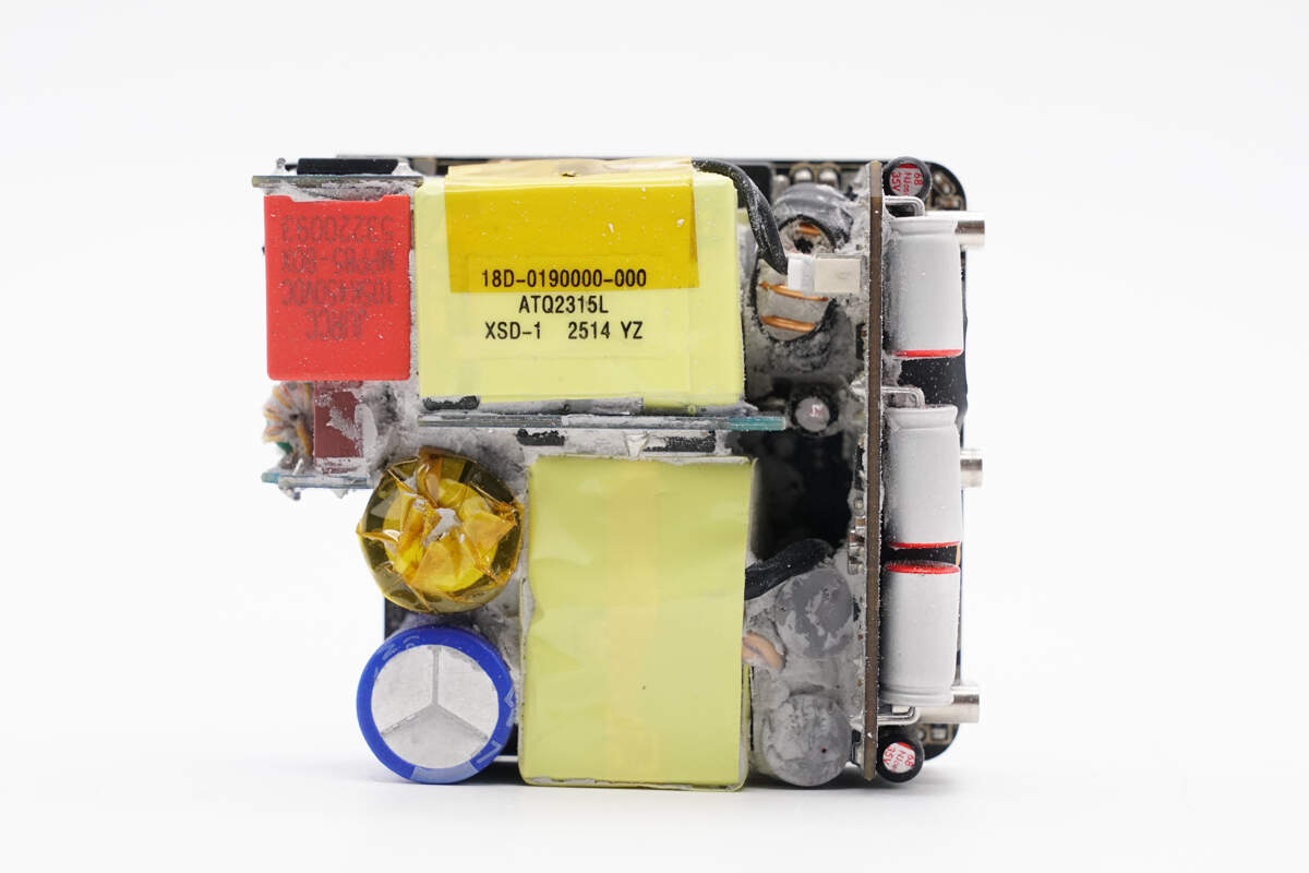
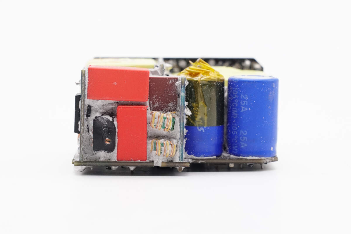
Clean off the potting compound. On the front left side of the PCBA module is the input section, where the fuse PCB and bridge rectifier PCB are soldered. Above that is the PFC PCB, below are the high-voltage filter capacitor and transformer. The capacitor for output filtering is insulated with a silicone sleeve. On the right side is the buck output PCB.
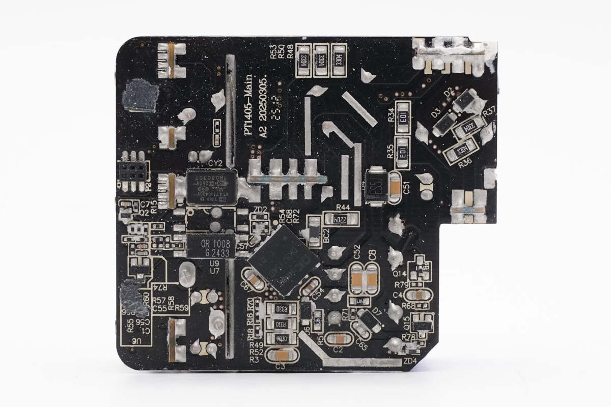
The back side is equipped with an AHB GaN chip, an SMD Y capacitor, and a feedback optocoupler.
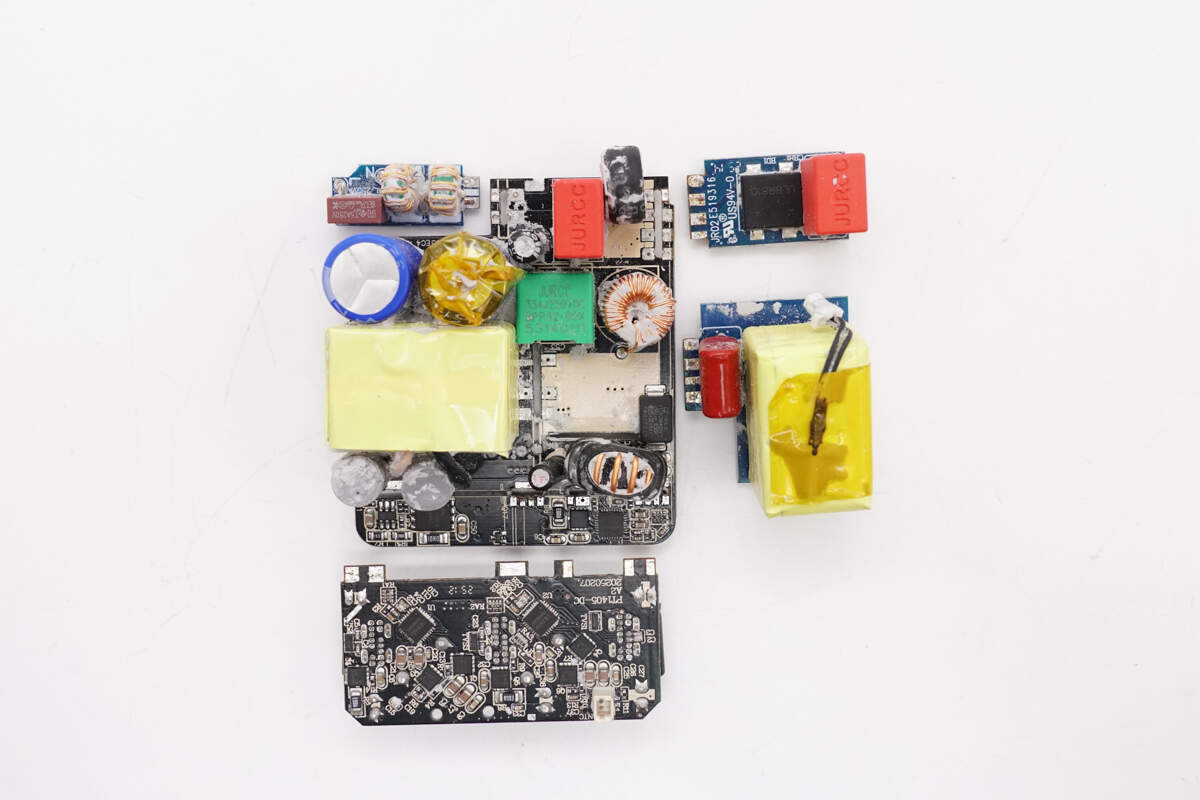
Disassemble each small PCB. Through observation of the PCBA modules, it was found that it adopts a PFC + AHB architecture. The output section uses three synchronous buck chips. The PFC MOSFET is from Navitas, and the AHB stage uses a GaN chip from DONGKE.
The AHB architecture improves conversion efficiency by recycling the leakage inductance energy typically lost in traditional flyback designs, while retaining the wide output voltage range advantages of the flyback topology. DONGKE's highly integrated AHB GaN co-packaged chip is well-suited for high-power single-port PD fast charging applications. In fixed-voltage output scenarios for multi-port fast chargers, its conversion efficiency can rival that of LLC converters, while offering a cost advantage.
Two small PCBs are soldered together at the input to form the EMI circuit, improving space utilization and reducing overall size. The high-voltage filter capacitor on the right is wrapped with high-temperature insulation tape for safety.
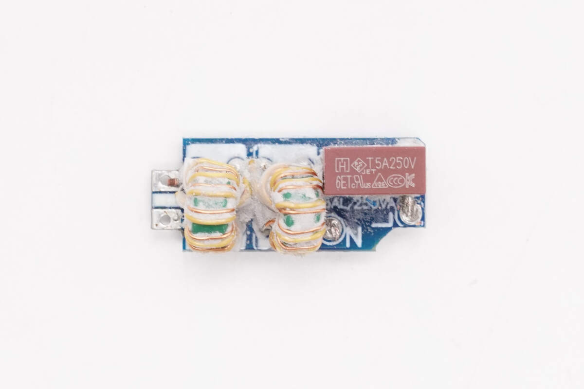
A fuse and two common mode chokes are soldered on the front side of the input PCB.
There are no components on the back.
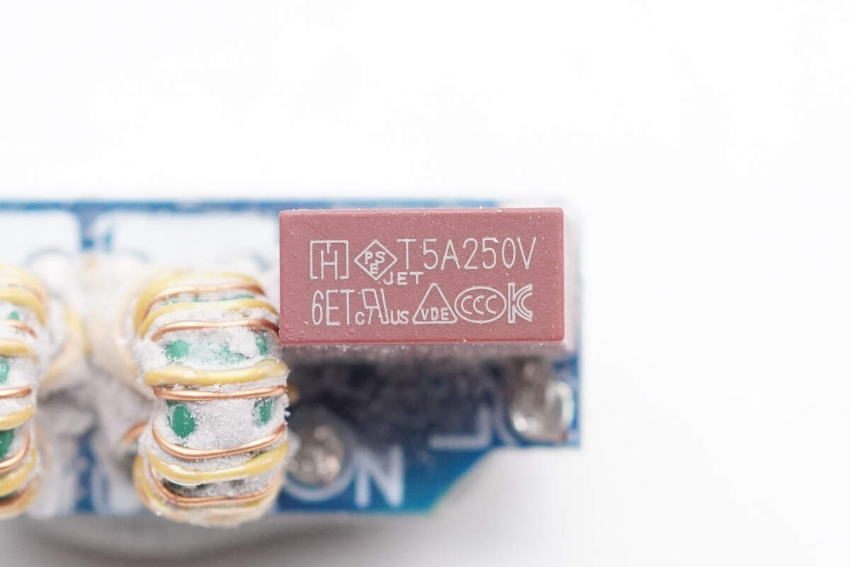
The input fuse is rated at 5A, 250V.
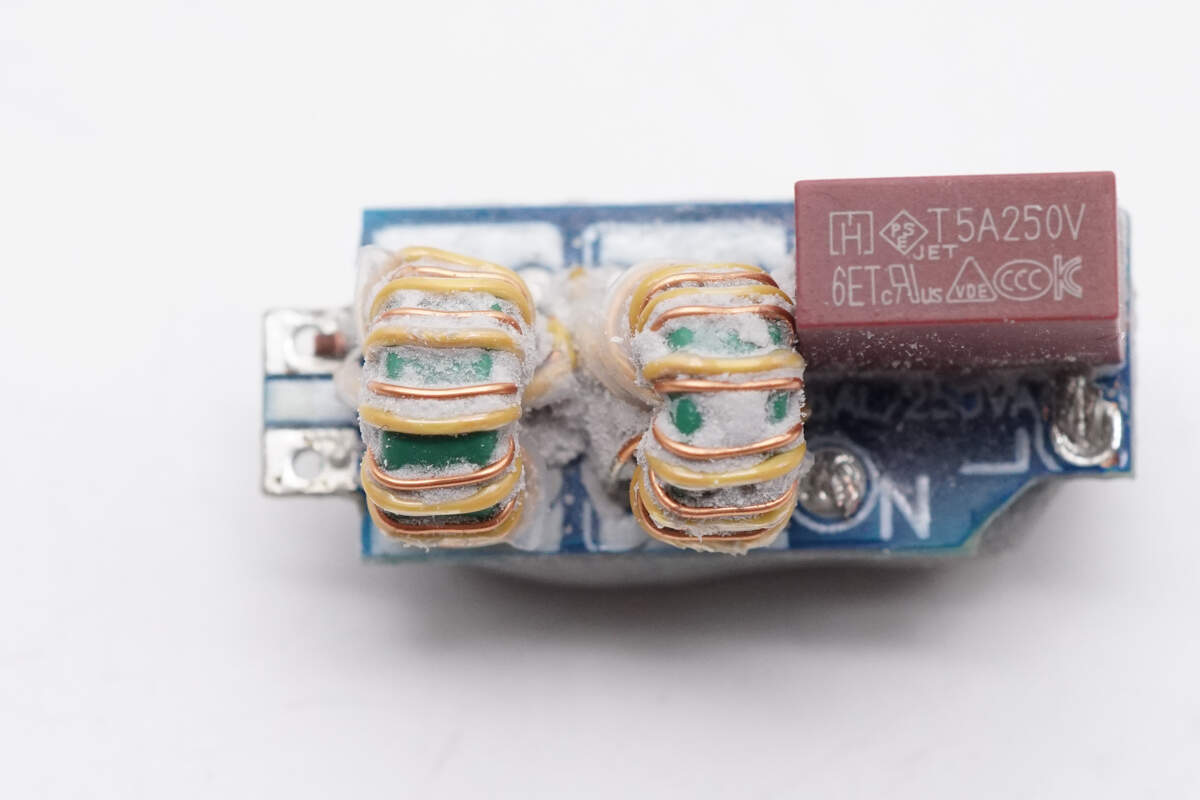
The common mode chokes are wound using enameled wire and insulated wire.
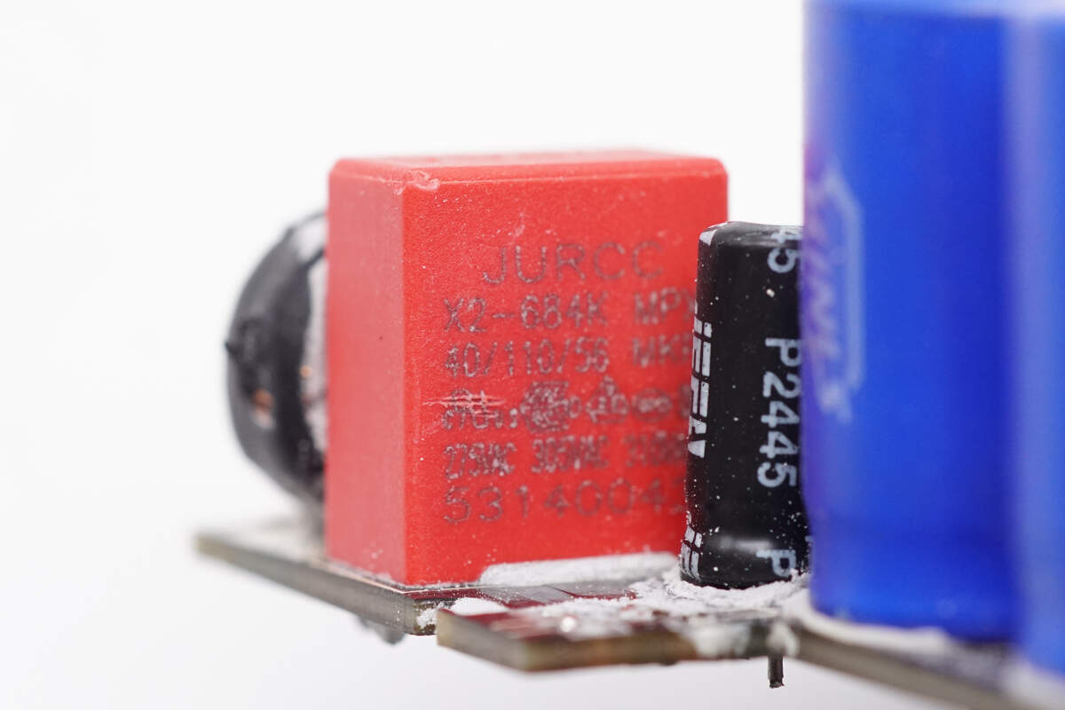
The safety X2 capacitor is from JURCC. 0.68μF.
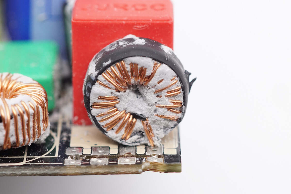
The filter inductor is wounded with a magnetic ring and insulated by heat-shrinkable tubing.
A thermistor is attached to the PFC inductor for temperature sensing. Below it are a film capacitor and a filter inductor. On the right side, a small PCB is soldered with a bridge rectifier.
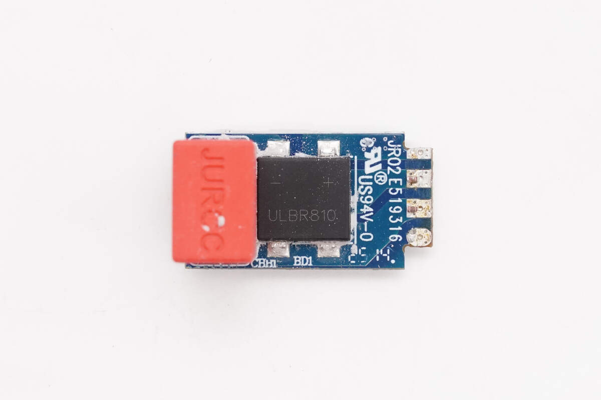
Another small PCB houses a bridge rectifier and a film capacitor.
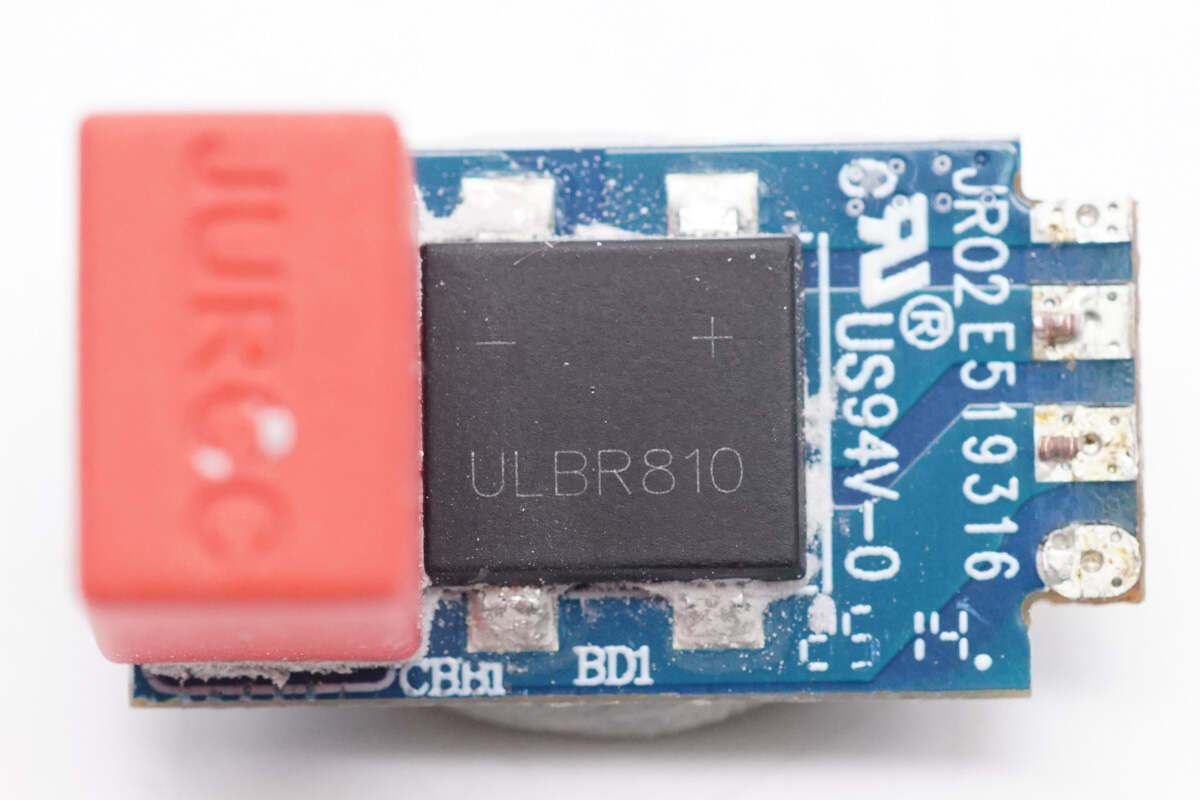
The bridge rectifier is marked with ULBR810. 8A 1000V.
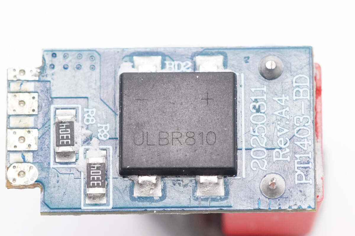
The back features another bridge rectifier of the same model, configured in a half-bridge connection. This setup helps distribute heat more evenly and reduces temperature rise.
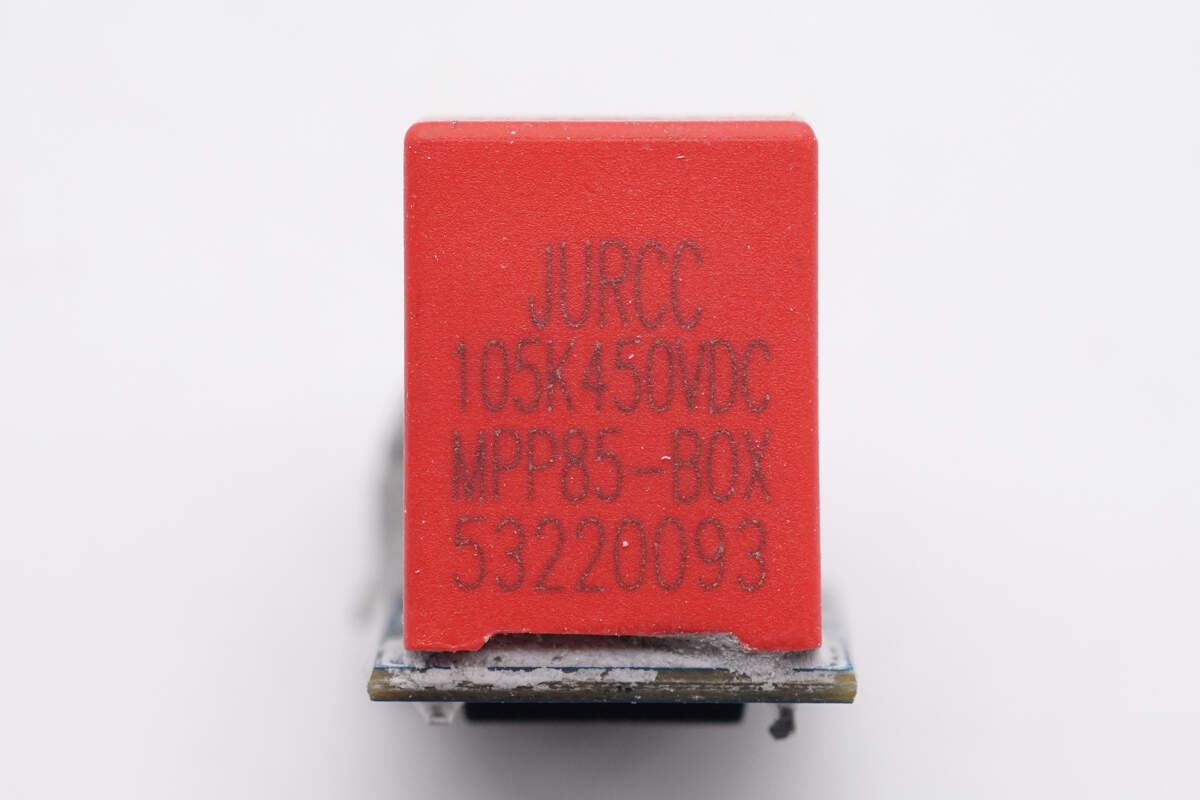
The film capacitor is from JURCC. 1μF 450V.
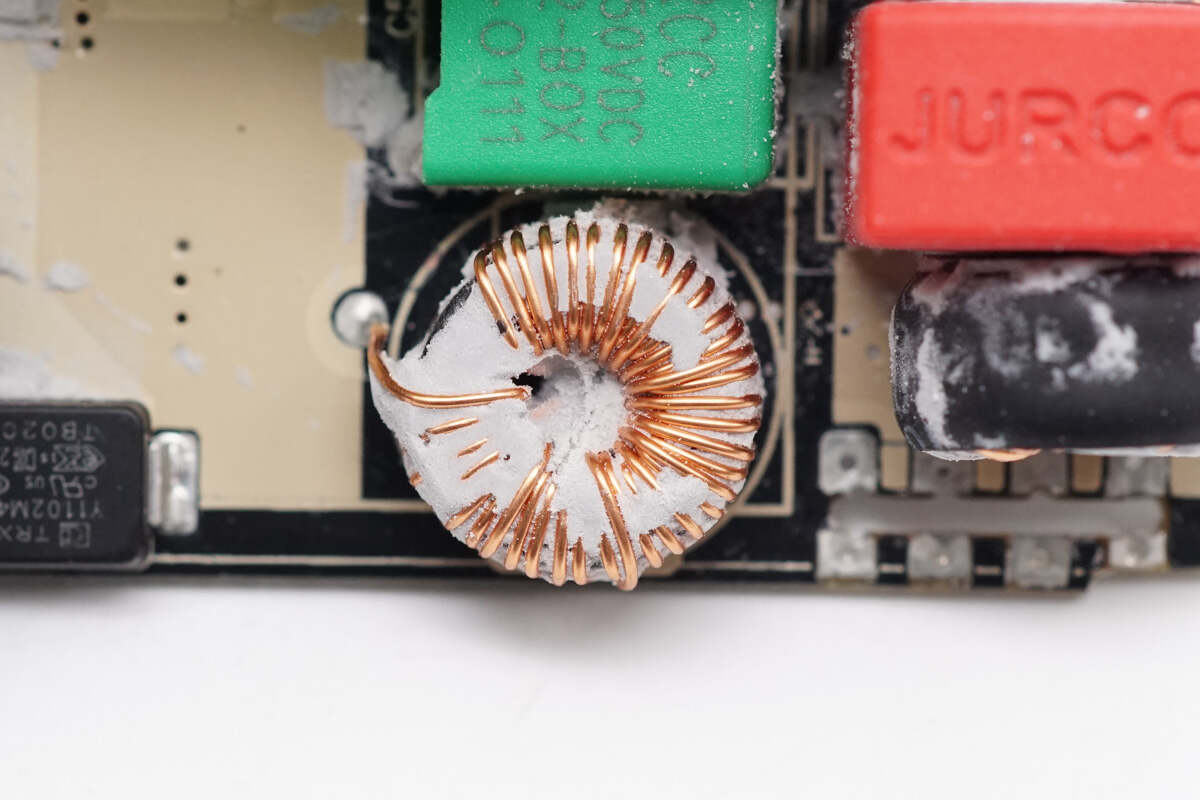
Close-up of the filter inductor soldered below the PFC inductor.
The PFC PCB is soldered with the PFC controller, PFC MOSFET, and PFC rectifier diode.
The other side features a boost inductor and a film capacitor.

The film capacitor is rated at 1 μF, 450 V.
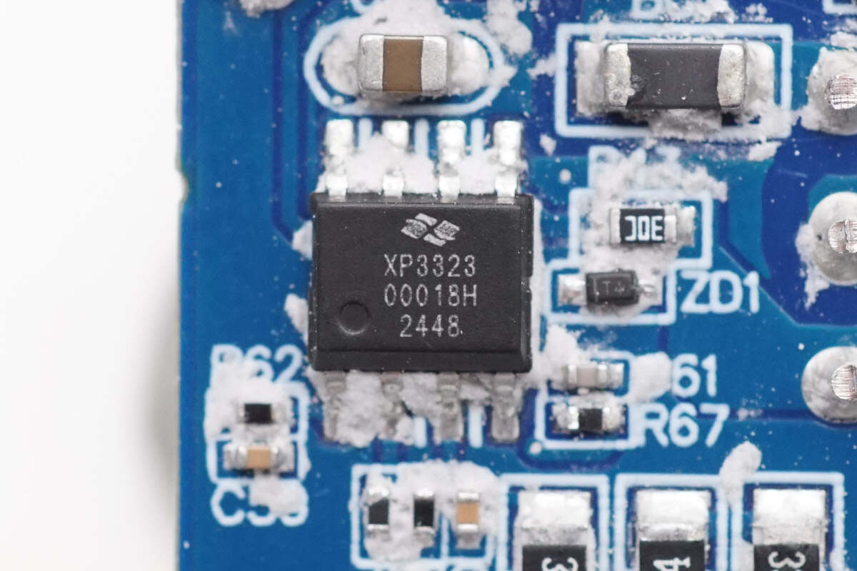
The PFC controller is from X-Signal, model XP3323. It is a boundary mode PFC controller that uses a patented digital power control algorithm, offering excellent dynamic performance and light-load PF/THD characteristics. It comes in an SOP-8 package.
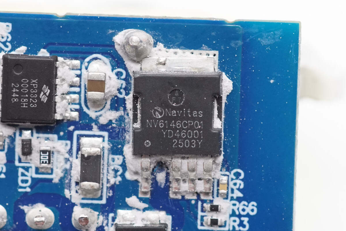
The PFC MOSFET is from Navitas, model NV6146C, part of the GaNSlim series. It integrates a high-performance 700V, 170mΩ enhancement-mode GaN device, with a built-in gate driver and lossless current sensing. It also supports over-temperature protection. The NV6146C is suitable for applications such as fast charging, wireless power transfer, LED lighting, solar micro-inverters, and server power supplies. It comes in a DPAK-4L package.
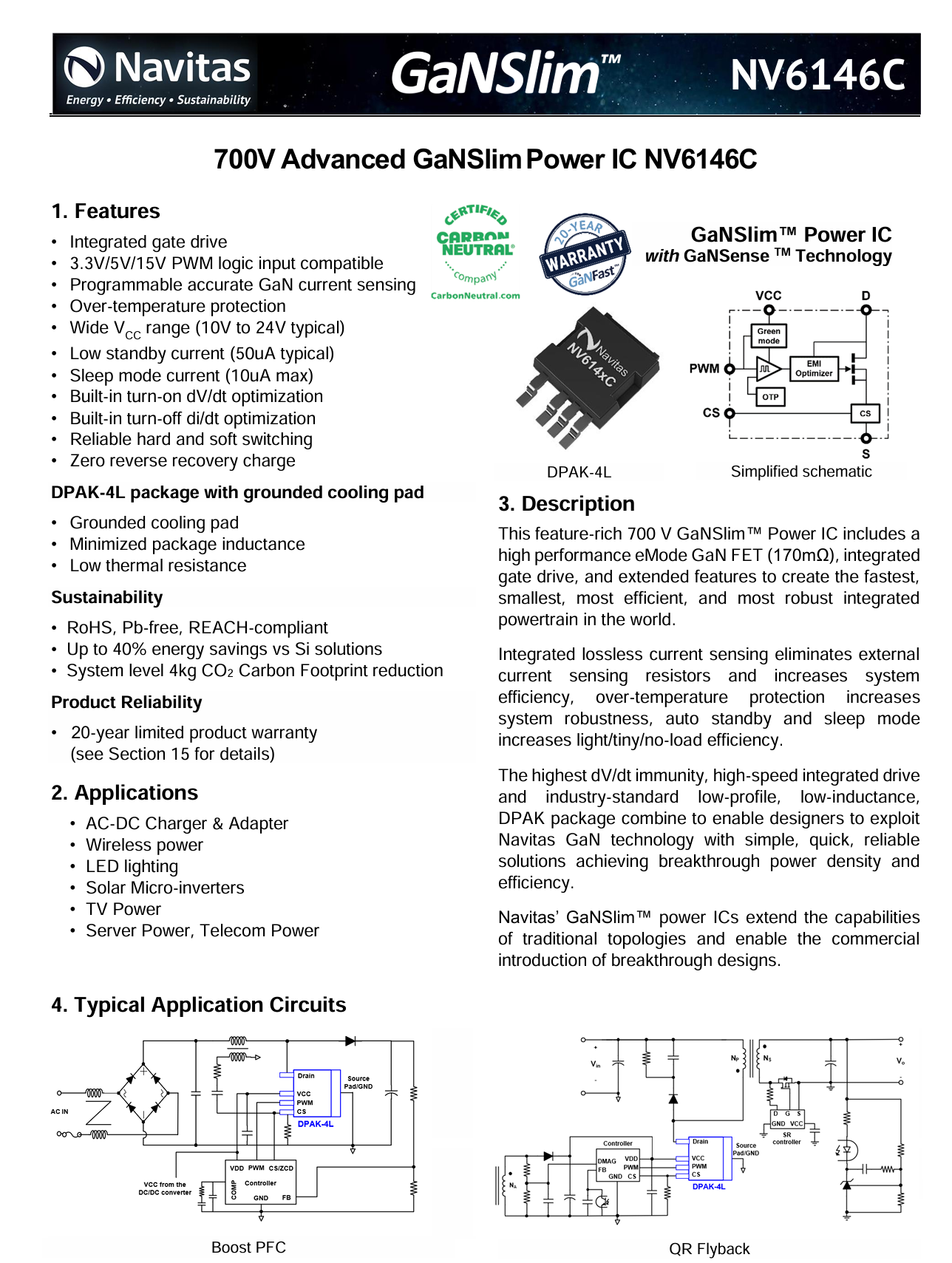
Here is the information about Navitas NV6146C.
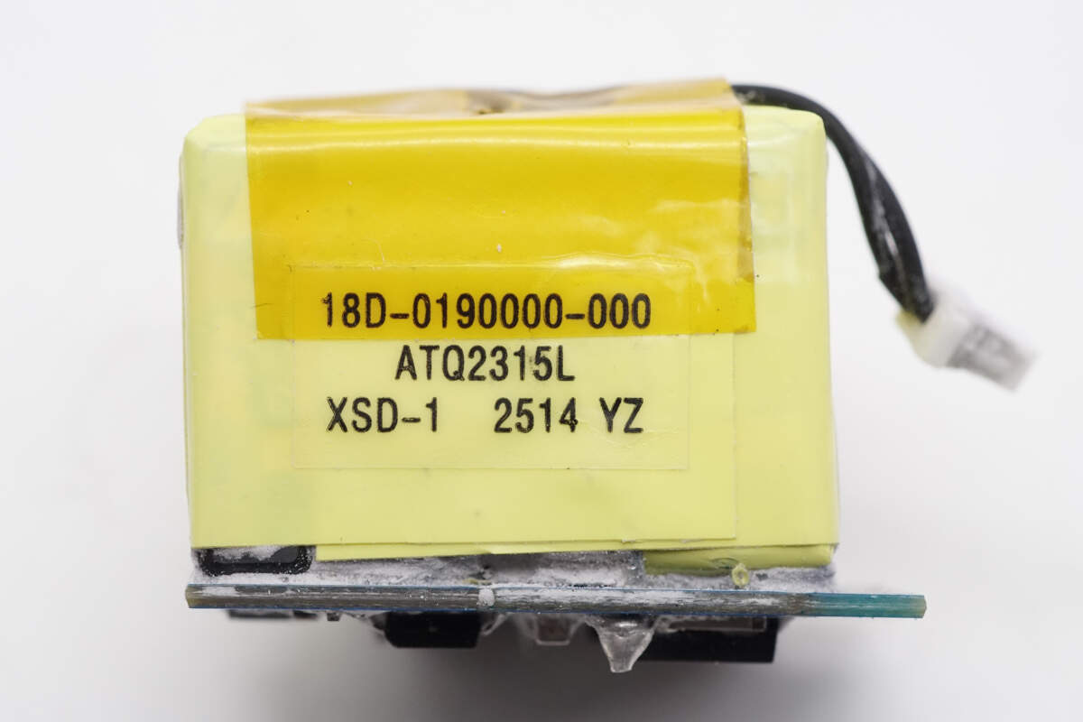
The PFC boost inductor uses an ATQ2315L magnetic core.
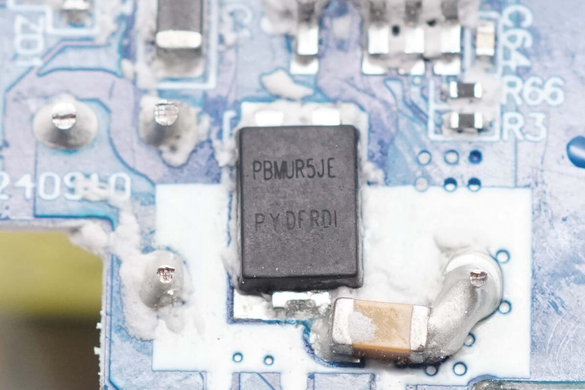
The PFC rectifier is from Pingwei, model PBMUR5JE. It is an ultrafast recovery diode rated at 600V, 5A, and comes in a PS-277B package.
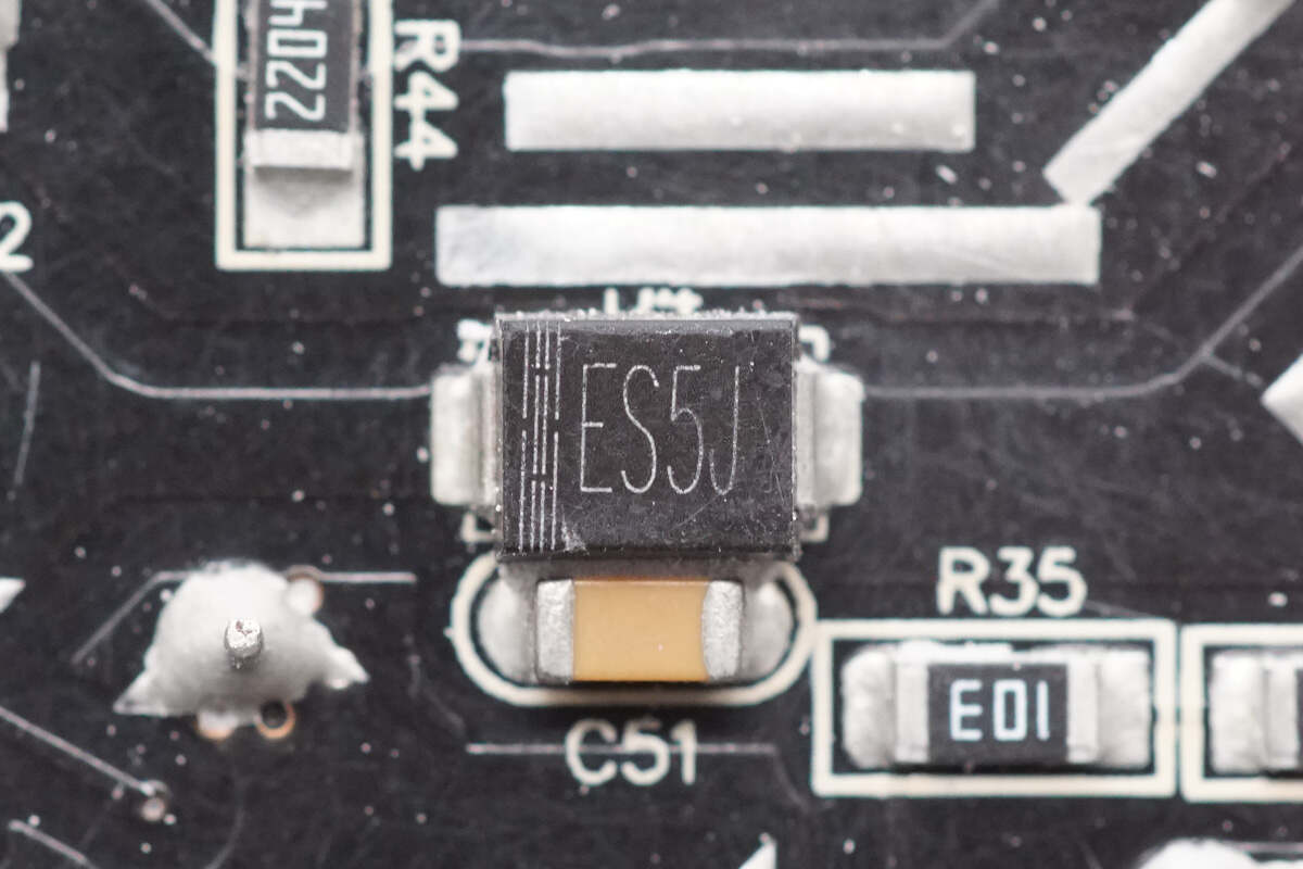
The ES5J diode is used for PFC bypass.
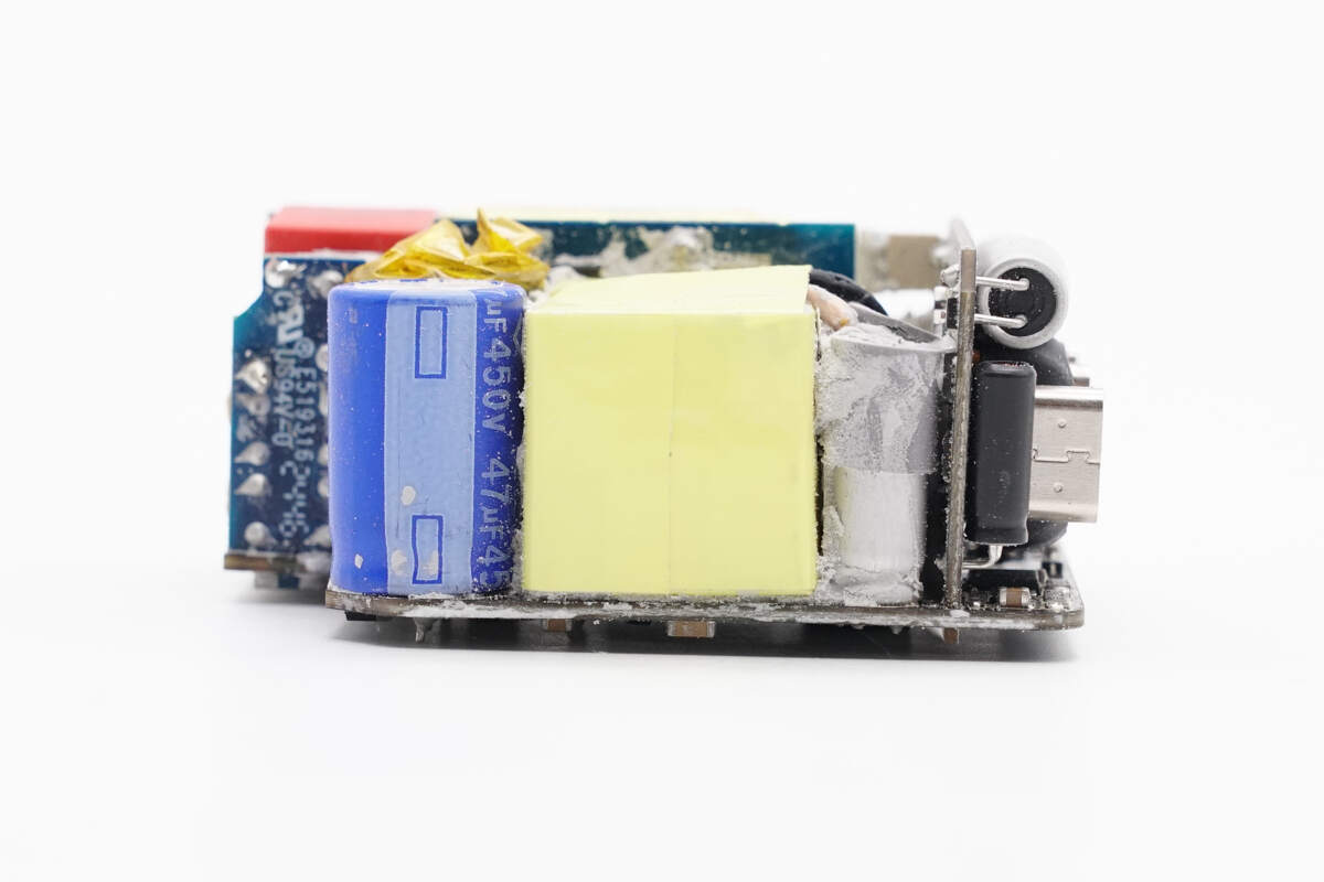
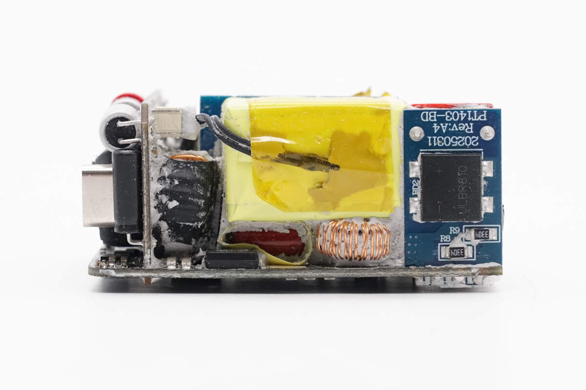
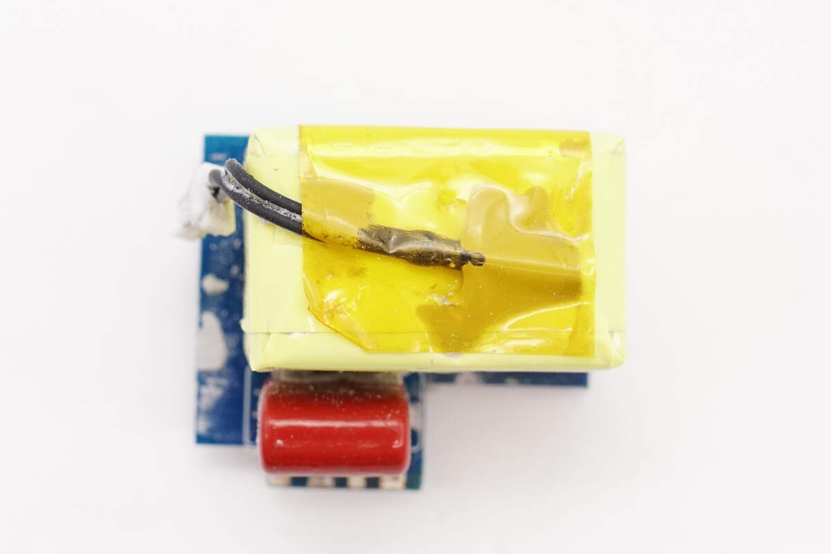
This side of the PCBA module features a high-voltage filter capacitor, transformer, solid capacitor, and a small output PCB.

The high-voltage filter capacitor is from KINLS. 47μF 450V.
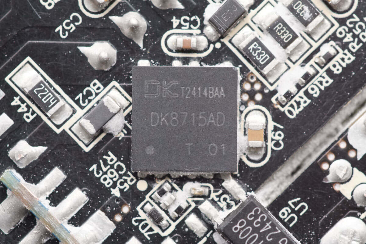
The AHB GaN chip is from DONGKE, model DK8715AD. It is an AC-DC power switch chip based on an asymmetric half-bridge architecture, integrating two GaN power devices. It enables primary-side ZVS and secondary-side ZCS over a wide load range, thereby improving overall system efficiency. Soft-switching also reduces stress on the power devices. An integrated full-range spread-spectrum circuit helps lower switching losses and improves EMI performance.
DK8715AD supports switching frequencies up to 800 kHz. With a front-end boost PFC stage, it is recommended for 150 W power applications. The standby power consumption is less than 50 mW. It features adaptive dead-time and shutdown algorithms that require no external adjustment, resulting in an extremely simplified peripheral design. The chip is halogen-free, RoHS compliant, and integrates high-voltage startup and X-capacitor discharge circuits, offering higher system performance and reliability.
DK8715AD supports four adaptive load modes, significantly improving efficiency across different load conditions. When using DK8715AD, the power conversion efficiency can reach up to 95.4%.
The DK8715AD integrates two 650V enhancement-mode GaN HEMTs, along with built-in half-bridge driver and asymmetric half-bridge control circuits. The PMOSFET and NMOSFET feature adaptive dead-time and shutdown algorithms: the NMOSFET uses adaptive dead-time, while the PMOSFET uses adaptive shutdown time. This eliminates the need for external adjustments, greatly simplifying design and debugging. It is equipped with multifunctional pins that support demagnetization detection, output OVP, brown-in/out detection, and more. It also includes a negative CS voltage sampling function to enhance drive stability.
With a highly simplified peripheral circuit, the DK8715AD significantly streamlines the design and manufacturing of AC-DC converters, especially for products requiring high conversion efficiency and high power density. The chip provides comprehensive protection features, including overload protection, output overvoltage protection, output short-circuit protection, VCC over/under-voltage protection, VS pin fault protection, primary overcurrent protection, and over-temperature protection.
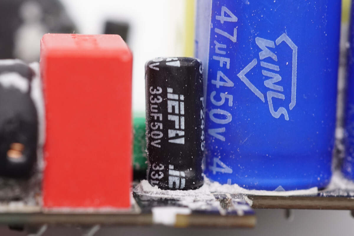
The filter capacitor for powering the master control chip is from Autochips. 33μF 50V.
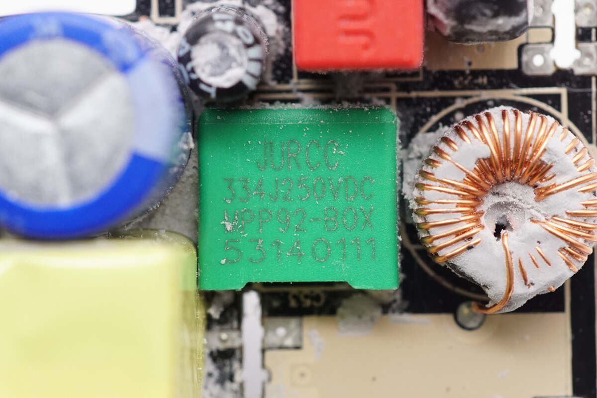
The resonant capacitor is from JURCC. 0.33μF 250V.
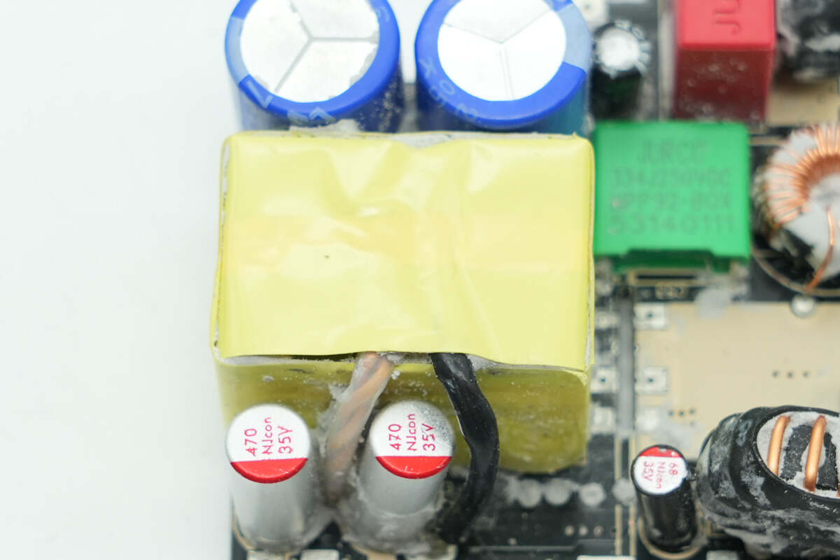
The transformer is tightly wrapped with insulating tape.
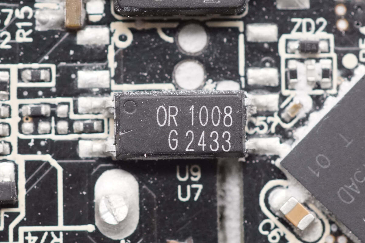
The OR OR1008 optocoupler is used for output voltage feedback regulation.
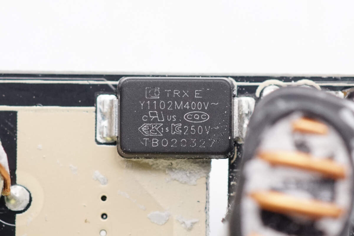
The SMD Y capacitor is from TRX. Its small size and light weight are suitable for high-density power products such as GaN fast chargers. The part number is TMY1102M.
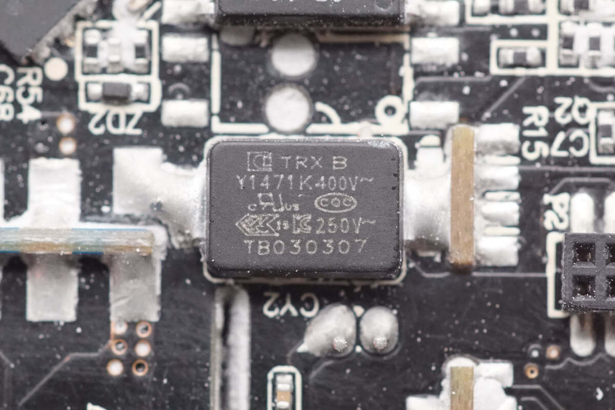
The other part number is TMY1471K.
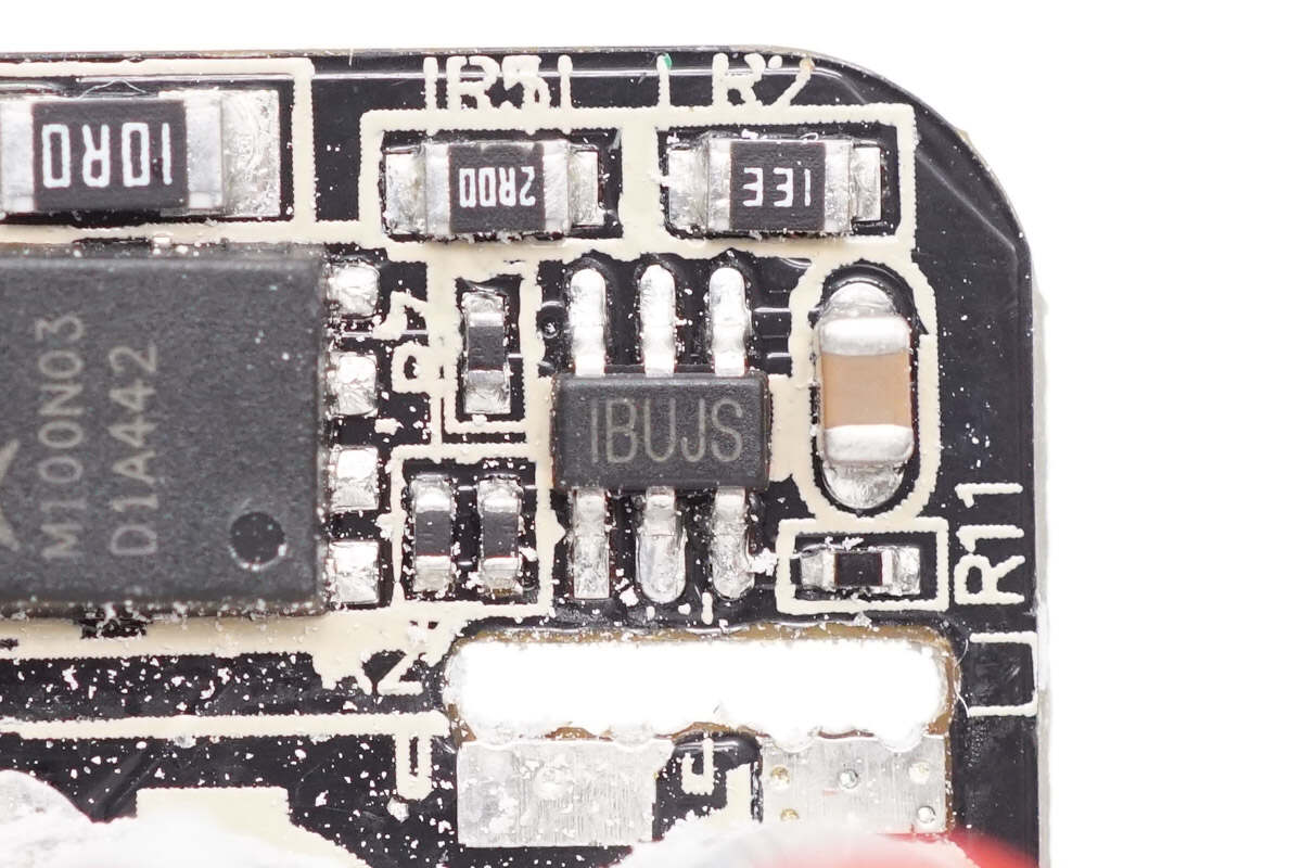
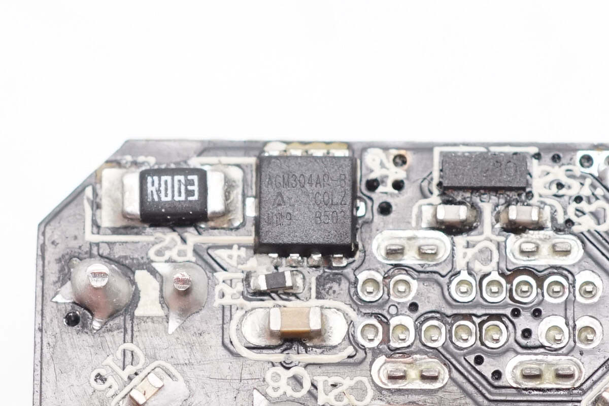
The synchronous rectifier controller is from MPS, marked with BUJ, model MP6951. It is MPS’s latest synchronous rectifier controller supporting DCM, CCM, QR, and ZVS operating modes. It also supports ACF active clamp flyback and HFB hybrid flyback topologies. The controller operates at frequencies up to 1 MHz and supports driving GaN synchronous rectifiers. It is suitable for both high-side and low-side applications and comes in a TSOT23-6 package.
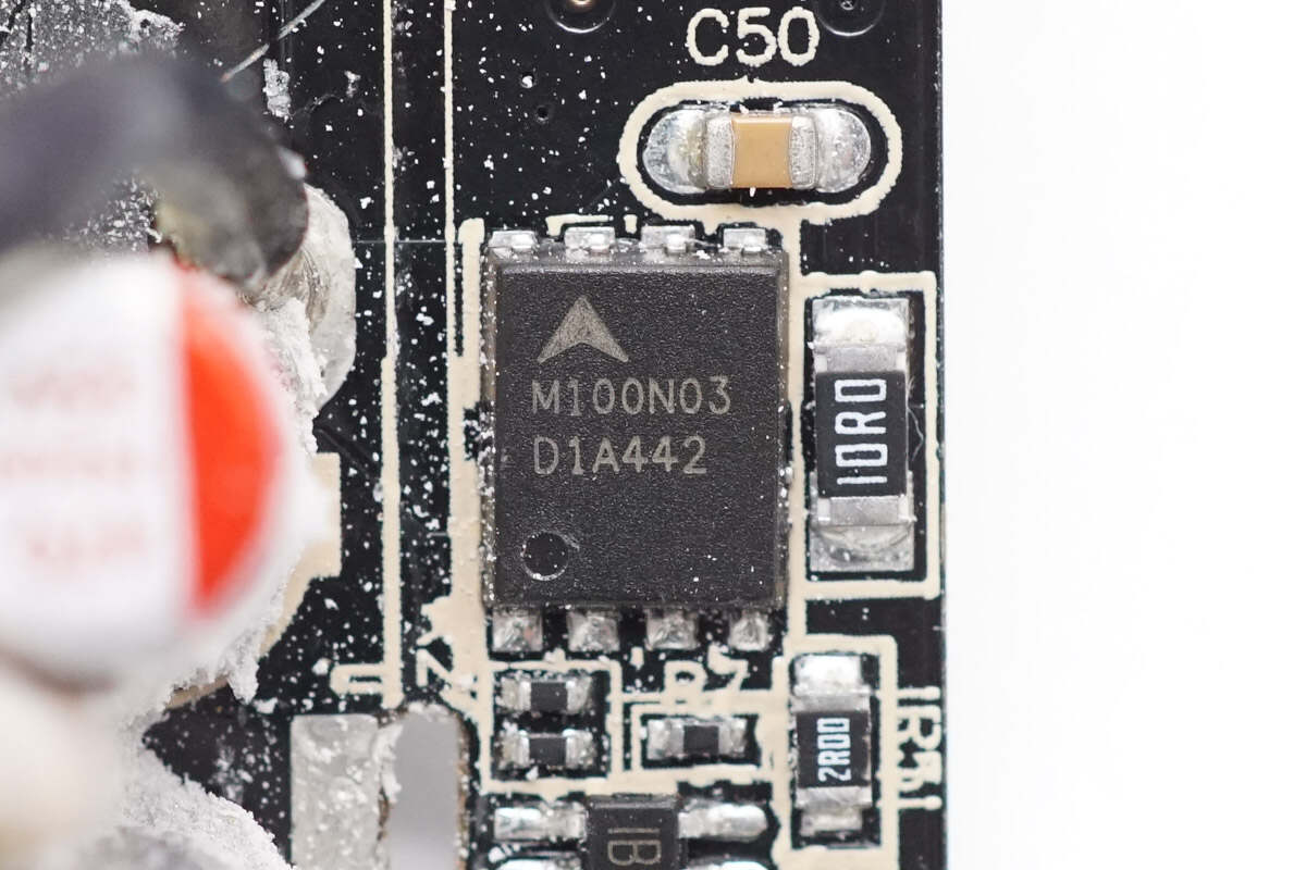
The synchronous rectifier is from ARK, marked with M100N03, model AKCM100N03DC8. It is an N-channel MOSFET with a voltage rating of 100V and an on-resistance of 5.2mΩ, packaged in a DFN 5×6 case.
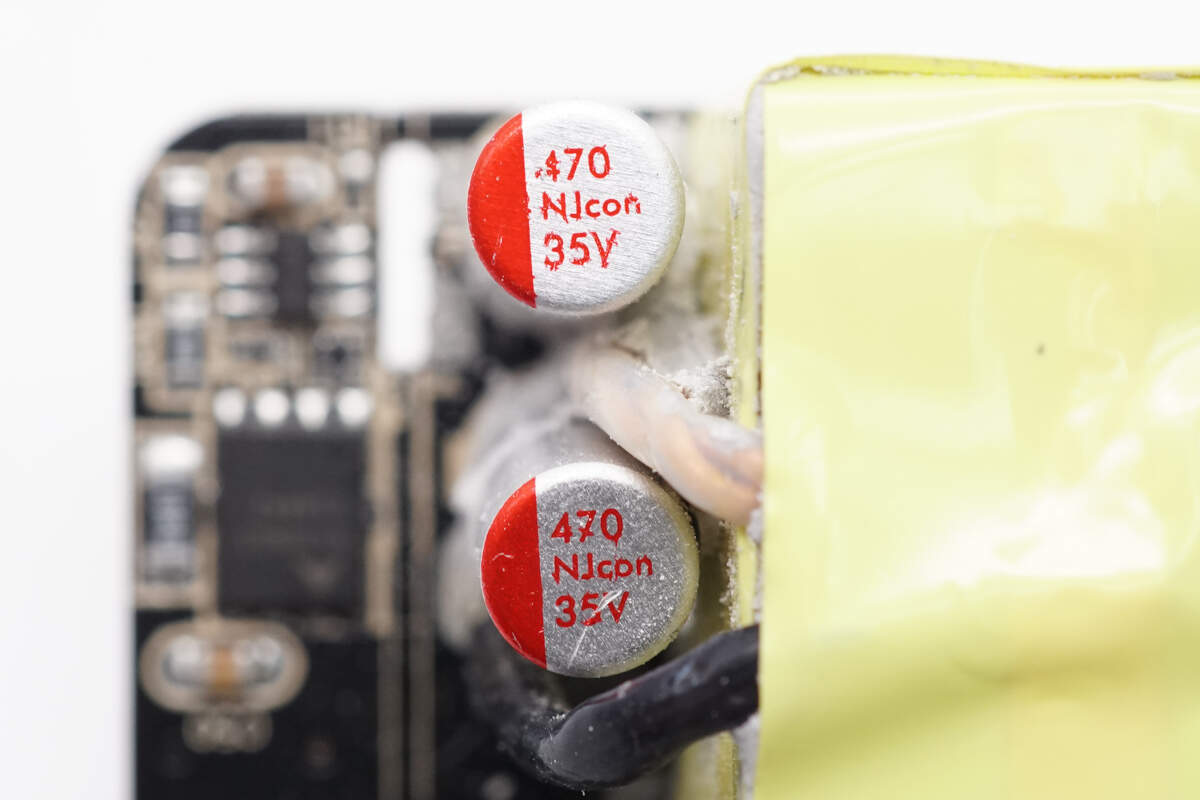
The solid capacitors are from Winner, rated at 470μF 35V, connected in parallel with two units.
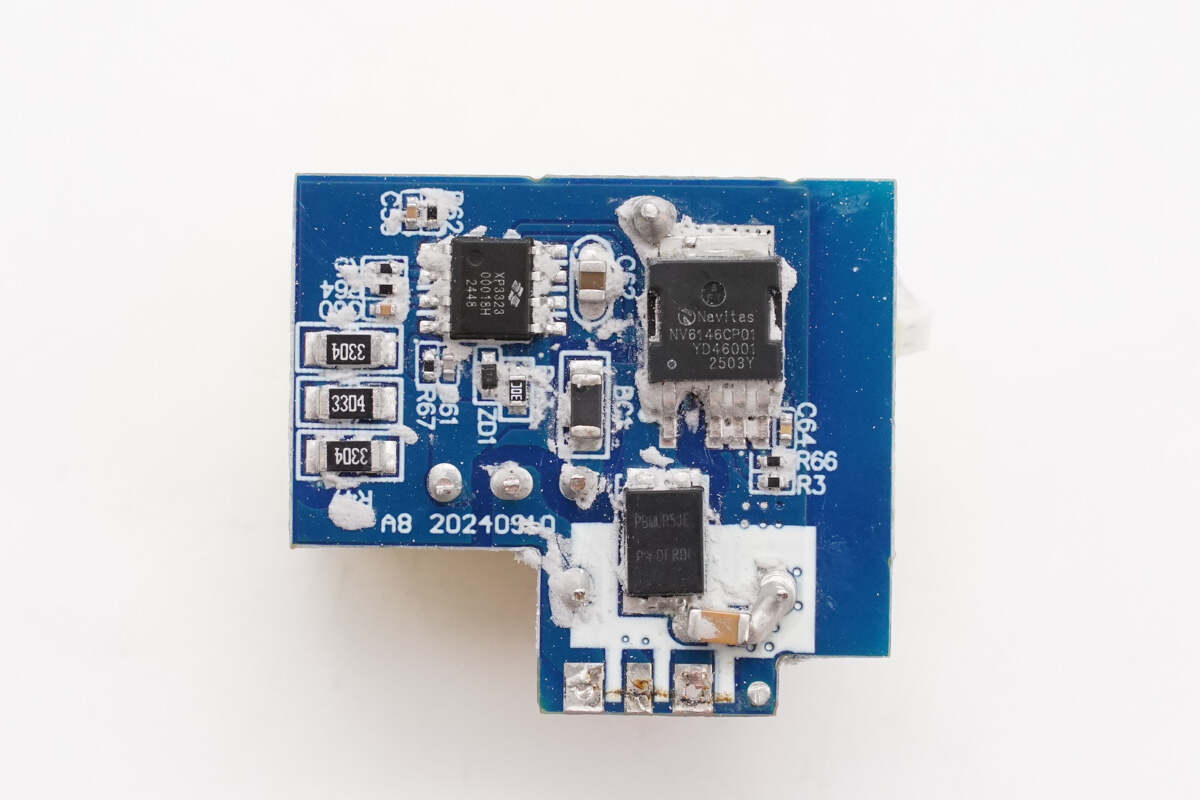
This small PCB is soldered vertically at the output end.
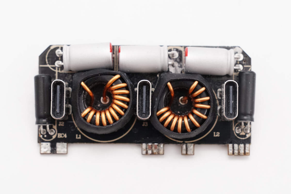
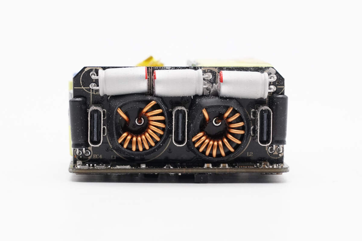
The PCB features three USB-C sockets, two magnetic buck inductors, and several filter capacitors.
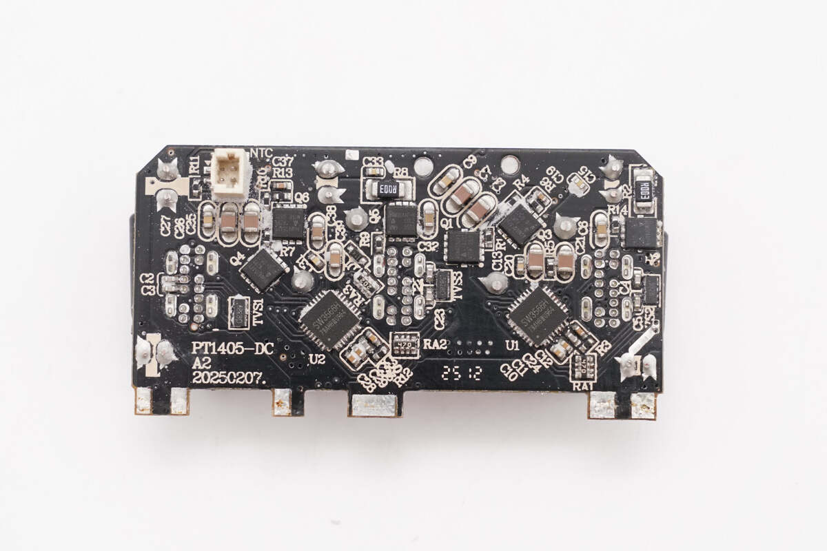
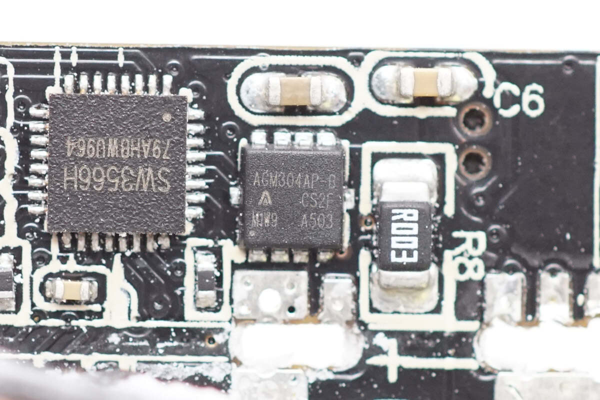
On the back side, the PCB is soldered with the buck protocol chips, the corresponding synchronous buck MOSFETs, and the VBUS MOSFETs.
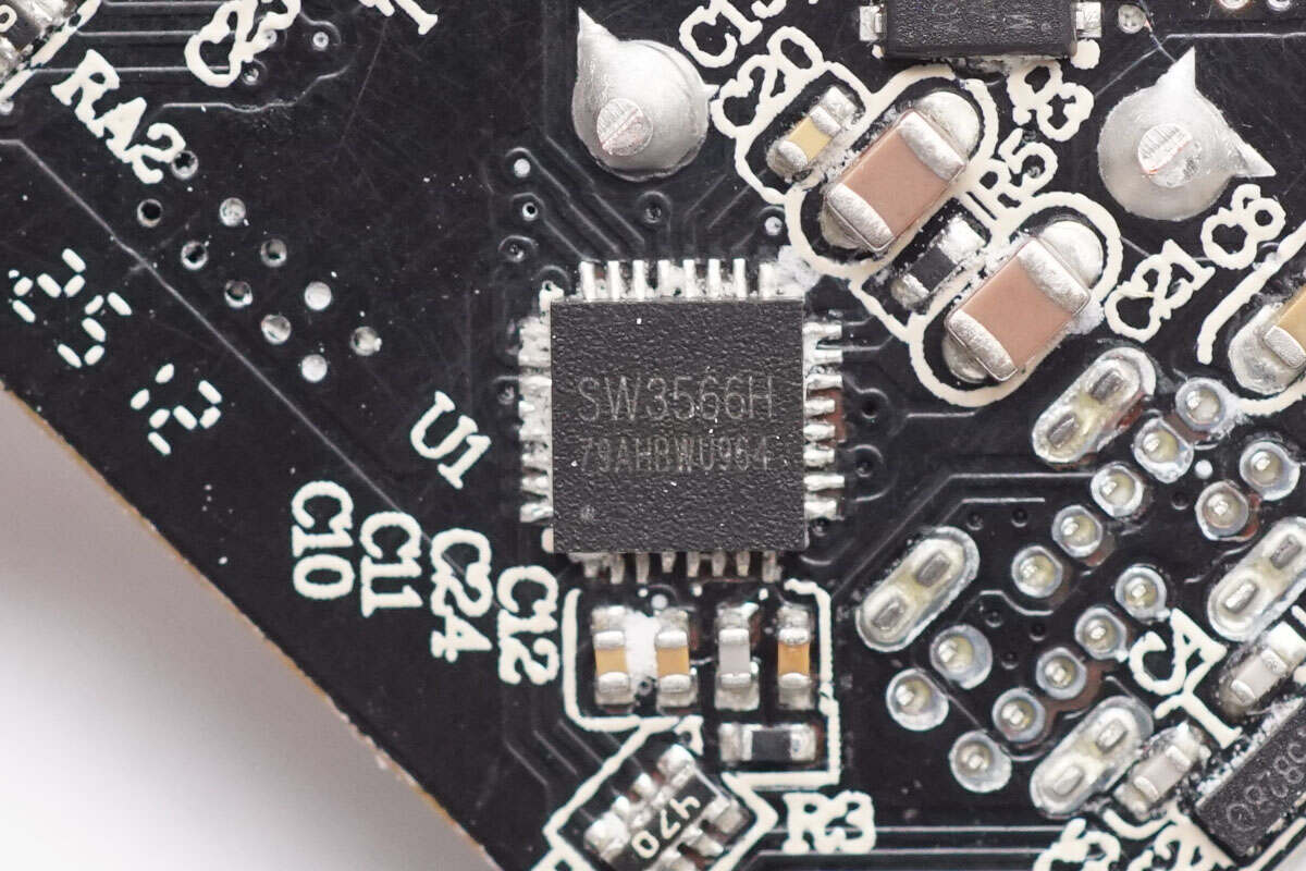
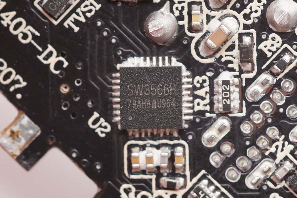
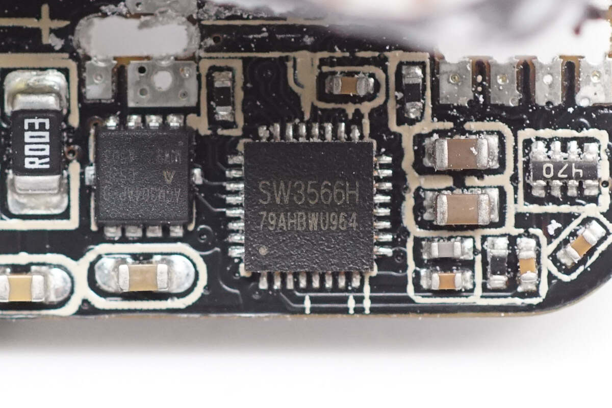
USB-C1 uses the iSmartWare SW3566H buck protocol chip. This highly integrated dual-port fast-charging SOC supports both USB-C and USB-A charging interfaces, with independent current limiting for each port. It features a built-in high-efficiency synchronous buck converter supporting 20V/7A and 28V/5A outputs. The chip supports fast-charging protocols including PD 3.1, QC, SCP, and UFCS, as well as customizable fast-charging protocols, with a maximum output power of up to 140W.
The SW3566H integrates CC/CV modes, dual-port management logic, and bus voltage detection. Paired with the corresponding buck MOSFET and VBUS MOSFET, it can achieve dual-port buck output. The built-in buck converter operates at a switching frequency of 180 kHz and supports both PWM and PFM modes. Protection thresholds such as output current and line loss compensation can be set via the I²C interface. The internal ADC supports data sampling on nine channels, including input/output voltage, output current, and chip temperature, enabling external MCU parameter display.
The SW3566H supports up to 36 V input voltage and a maximum output current of 7 A. It features built-in soft-start, input overvoltage/undervoltage protection, output overvoltage/undervoltage protection, output overcurrent/short-circuit protection, DP/DM/CC overvoltage protection, chip over-temperature protection, external NTC thermistor protection, and power limiting protection. The chip comes in a QFN 4×4-32 package.
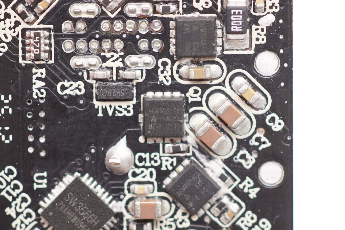
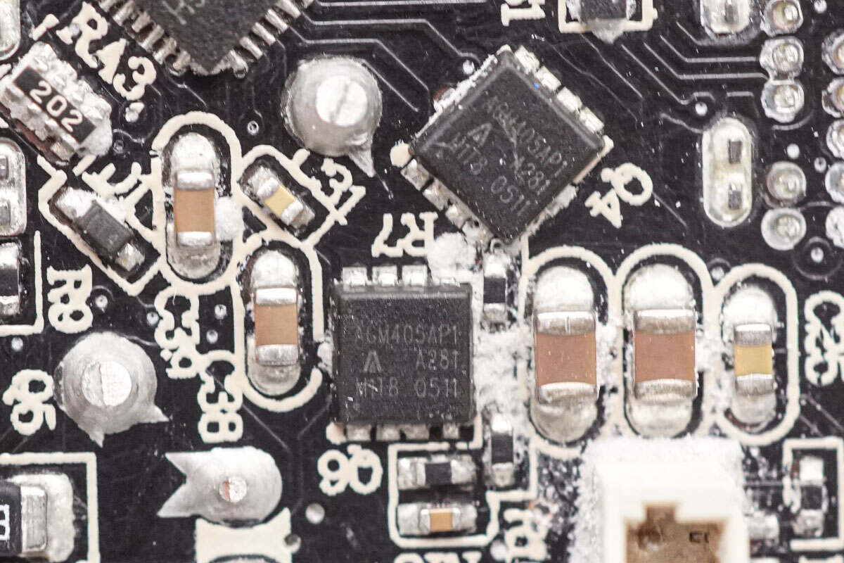
The synchronous buck MOSFET is from AGM-Semi, model AGM405AP1. It is an N-channel MOSFET rated at 40V with an on-resistance of 5.7mΩ, packaged in a PDFN 3.3×3.3 case.
The TVS diode for ESD protection on the USB-C interface is from Goaltop, marked 5B28O, model GESD5B284JDO. This device features an asymmetric design with two 5V bidirectional TVSs and two 28V unidirectional TVSs. It offers low leakage current and low clamping voltage, providing overvoltage protection for data lines and CC lines in PD applications. The package type is DFN 2.5×10.
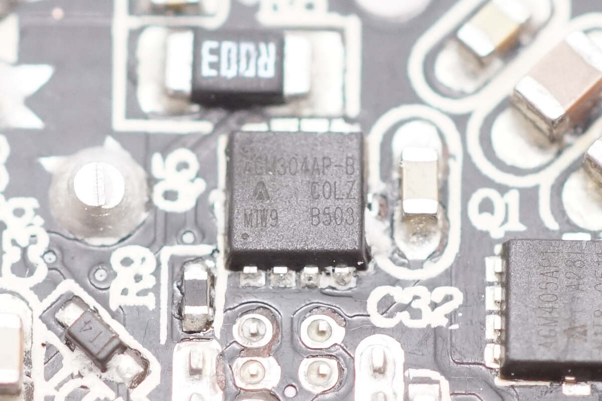
The VBUS MOSFET is from AGM-Semi, model AGM304AP-B. It is an N-channel MOSFET rated at 35V with an on-resistance of 3.1mΩ, packaged in a PDFN 3.3×3.3 case.
USB-C2 uses the iSmartWare SW3566H buck protocol chip.
The synchronous buck MOSFET uses AGM-Semi AGM405AP1.
The VBUS MOSFET uses AGM-Semi AGM304AP-B.
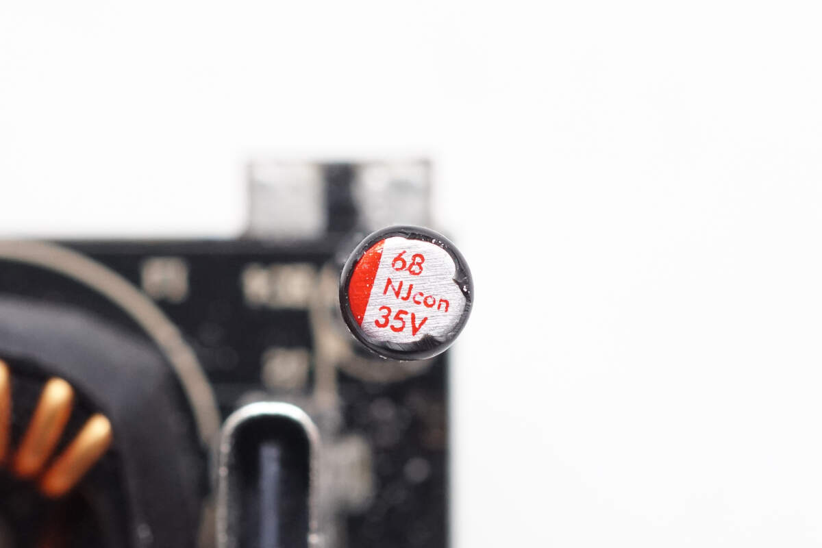
The input filter capacitor is from Winner. 68μF 35V.
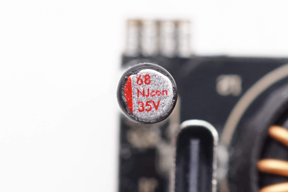
The other filter capacitor has the same specifications.
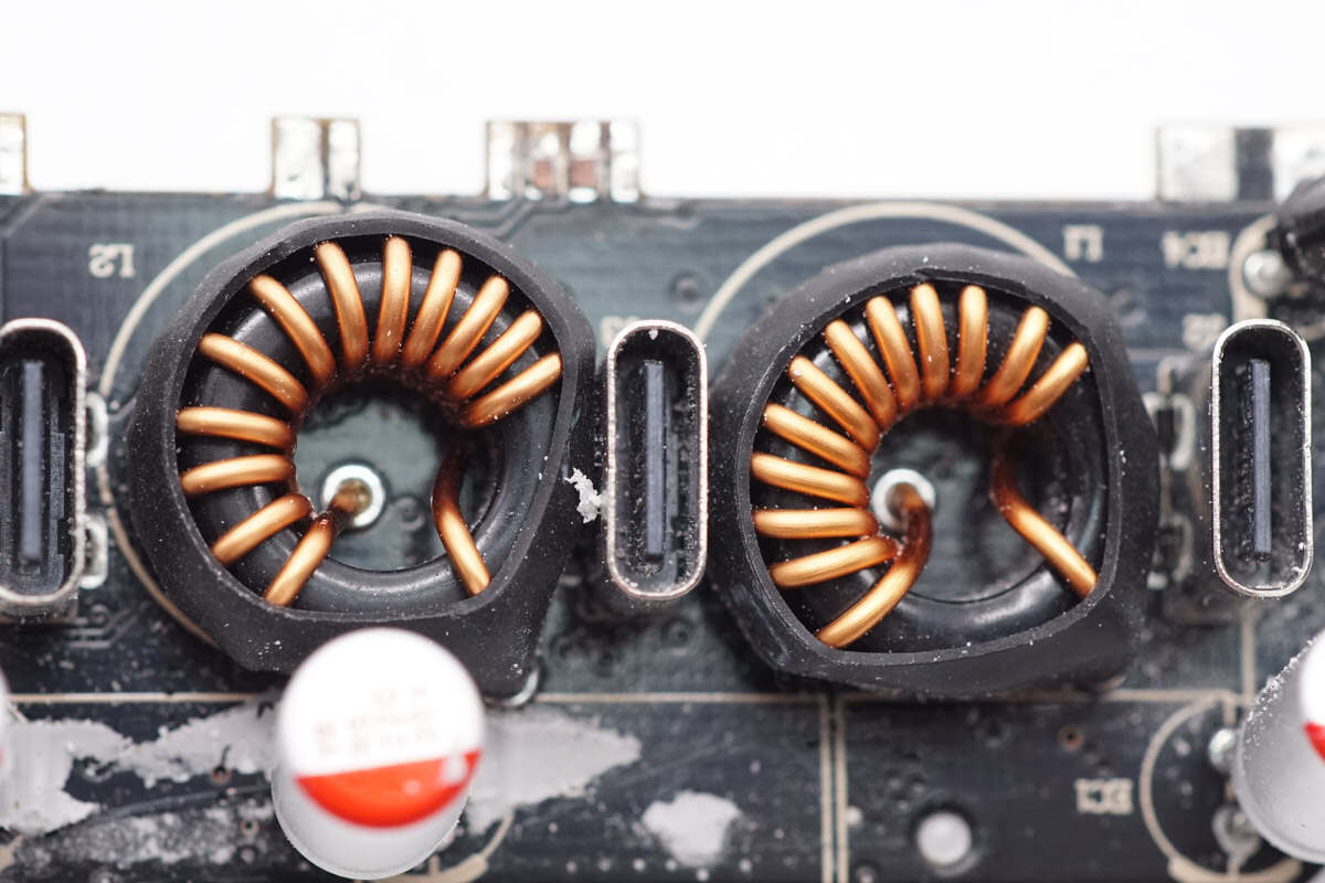
Two magnetic buck inductors are insulated with heat-shrink tubing.
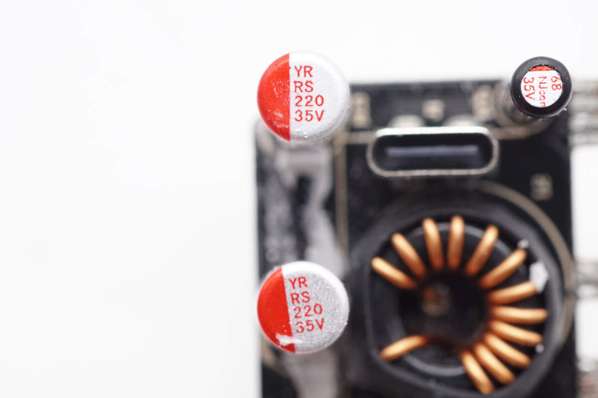
The two filter capacitors are rated at 220μF, 35V.
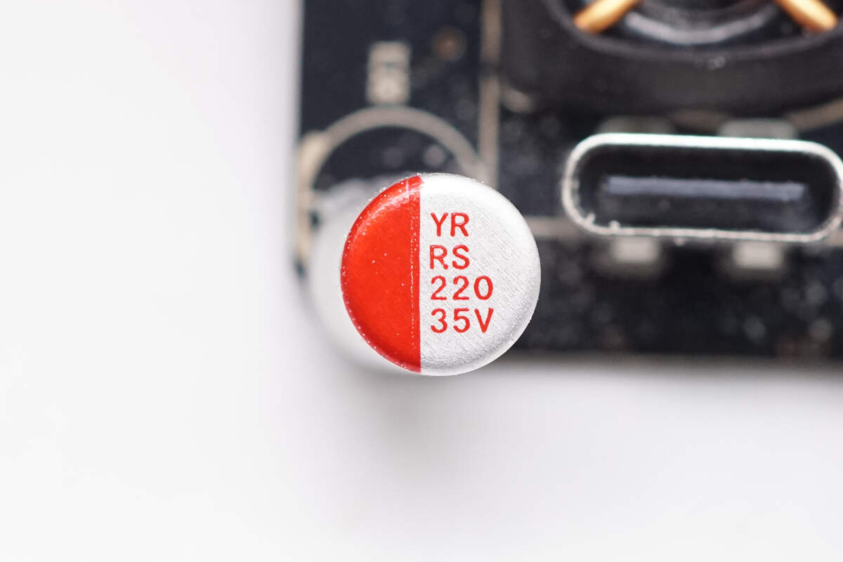
The third filter capacitor has the same specifications.
USB-C3 also uses the iSmartWare SW3566H buck protocol chip.
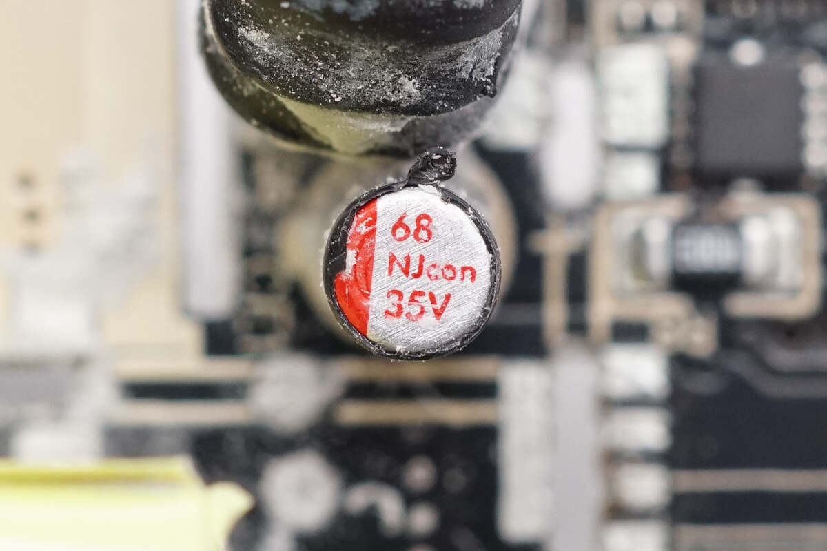
The input filter capacitor is rated at 68μF, 35V.
The magnetic buck inductor is insulated with heat-shrink tubing.
Below the buck inductor is the synchronous buck MOSFET, using AGM-Semi AGM405AP1.
The VBUS MOSFET uses AGM-Semi AGM304AP-B.
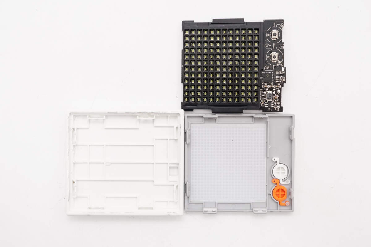
Pry open the dot matrix module casing along the gap.
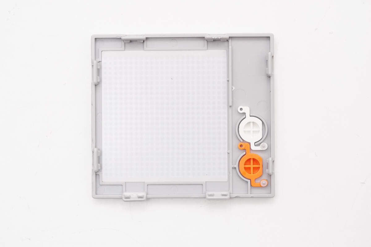
Inside the gray cover plate are a light guide plate and buttons.
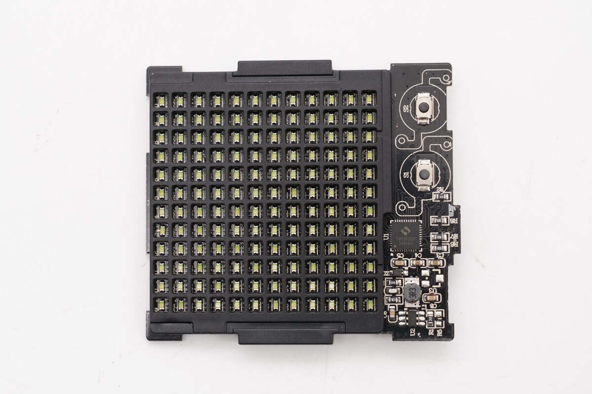
The front side of the PCBA module features SMD LED dot matrices, with SMD buttons and an MCU on the right.
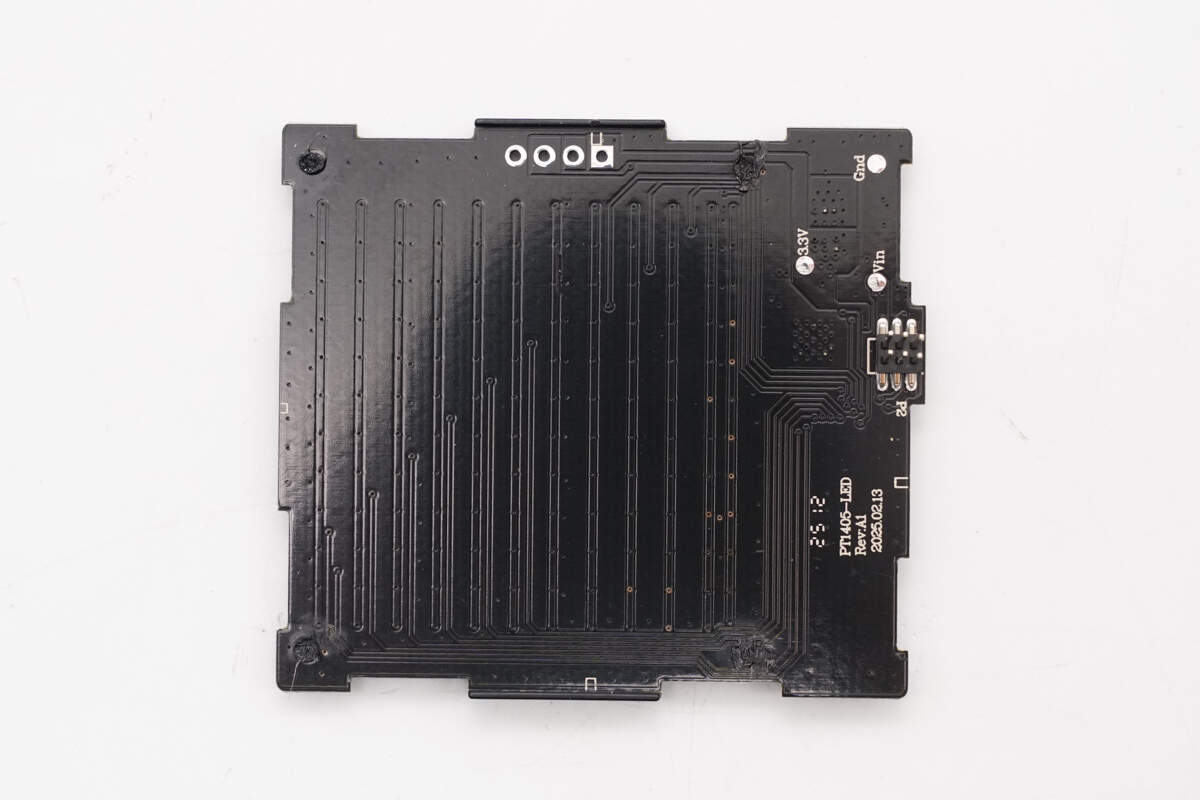
The back side of the module contains the LED wiring traces.
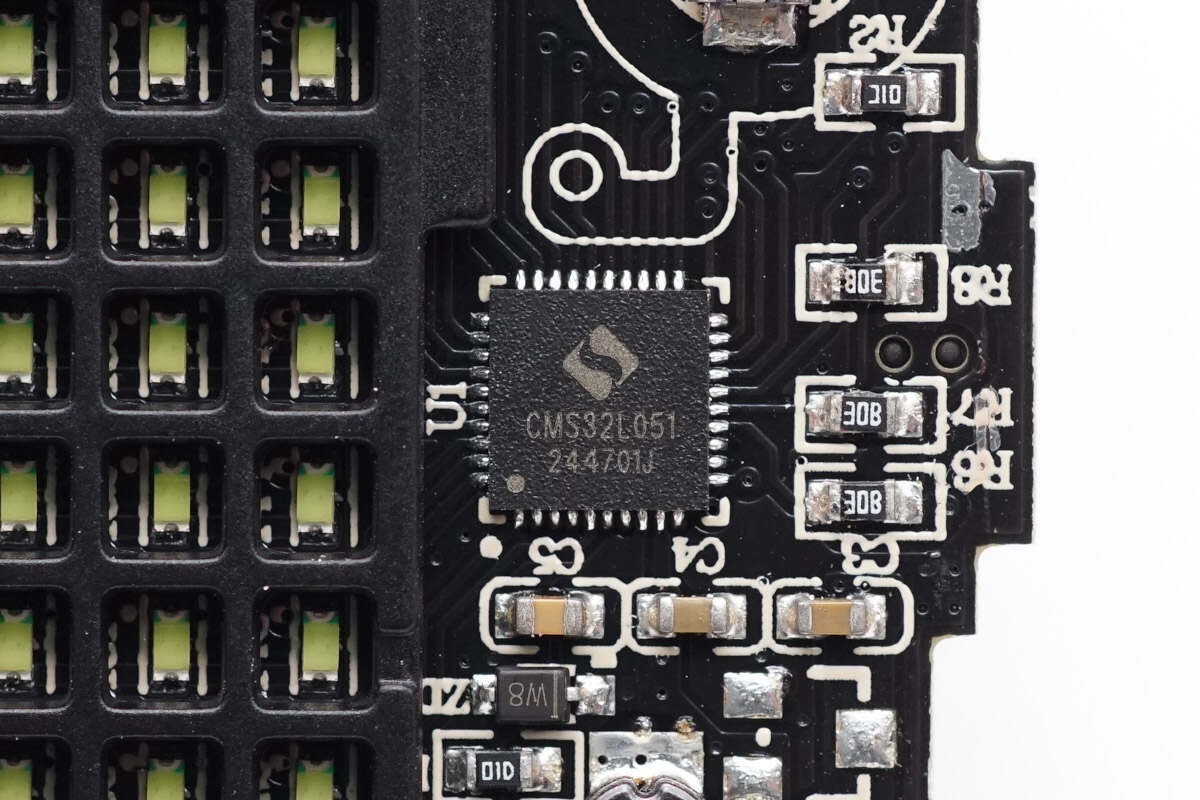
The MCU used for the dot matrix display control is from Cmsemicon, model CMS32L051. It features an ARM Cortex-M0+ CPU, 64KB of built-in FLASH, and 8KB of SRAM, and comes in a QFN40 package.
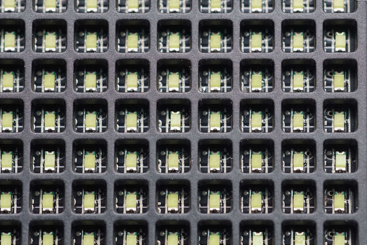
Close-up of the SMD LED lights, equipped with a plastic grid to block stray light.
Well, those are all components of the SHARGE Pixel 140 GaN Charger.
Summary of ChargerLAB
Here is the component list of the SHARGE Pixel 140 GaN Charger for your convenience.
It features foldable pins for easy portability. The charger has three USB-C ports and supports automatic power distribution when used simultaneously. The dot matrix display can show the total output power as well as the power of each port, with support for brightness and angle adjustments.
After taking it apart, we found that it is composed of multiple PCBs soldered together to fully utilize space. It uses a PFC + AHB architecture, featuring the X-Signal XP3323 PFC controller paired with the Navitas NV6146C GaN FET. The AHB GaN chip is the DONGKE DK8715AD.
It uses three iSmartWare SW3566H chips for buck output, paired with AGM-Semi MOSFETs. The charger includes an NTC thermistor for over-temperature protection, solid capacitors on the output, and TVS diodes on the USB-C ports for ESD protection. The PCBA module is filled with potting compound, with graphite sheets applied internally for heat dissipation. The workmanship and materials are solid and reliable.
Related Articles:
1. Teardown of MEGMEET MR750‑20V 15 kW DC Charging Module
2. Teardown of Belkin 240W Dual USB-C Braided Cable
3. Teardown of Lenovo Legion 245W GaN Adapter (LA245)