Introduction
Recently, Samsung released a 60W GaN charger specifically designed for its flagship smartphones to be launched in 2025 and beyond. In addition to using GaN technology and supporting 60W fast charging, the charger features a key innovation: achieving zero standby power consumption.
To achieve this, the product is based on the BPS BP87650A + BP62650A power solution and paired with its patented magnetic coupling communication feedback component BP818. This allows primary-to-secondary communication without a bias current, further eliminating standby losses caused by the feedback loop. As a result, the entire solution achieves power consumption as low as 2mW, far below the IEC62301 standard, leaving ample headroom for energy efficiency upgrades in higher-power fast charging products.
As a global leader in consumer electronics, Samsung clearly stated as early as 2021 that its mobile charger products, which previously met a 20mW standby standard, would be upgraded to a 5mW standard by 2025. The launch of this charger not only fulfills Samsung’s energy efficiency commitment but also establishes a new technical benchmark for the industry. The following sections detail the product’s specific design.
Product Appearance
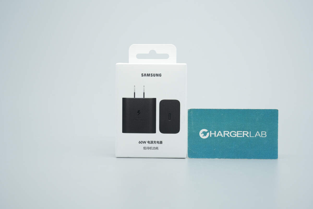
The front of the packaging displays the SAMSUNG brand, the product name, and images of the charger’s front and top views.
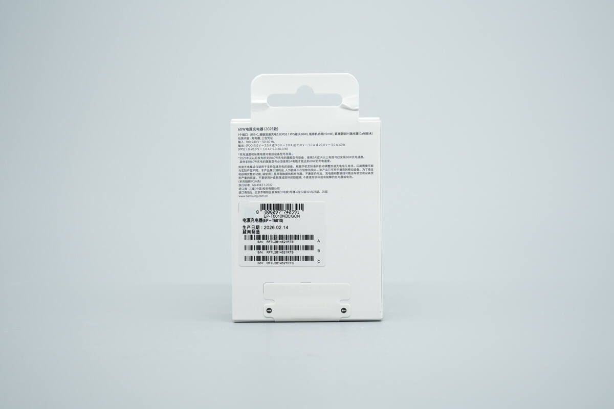
The back of the packaging displays the contents list, product specifications, manufacturing date, and relevant cautionary information.
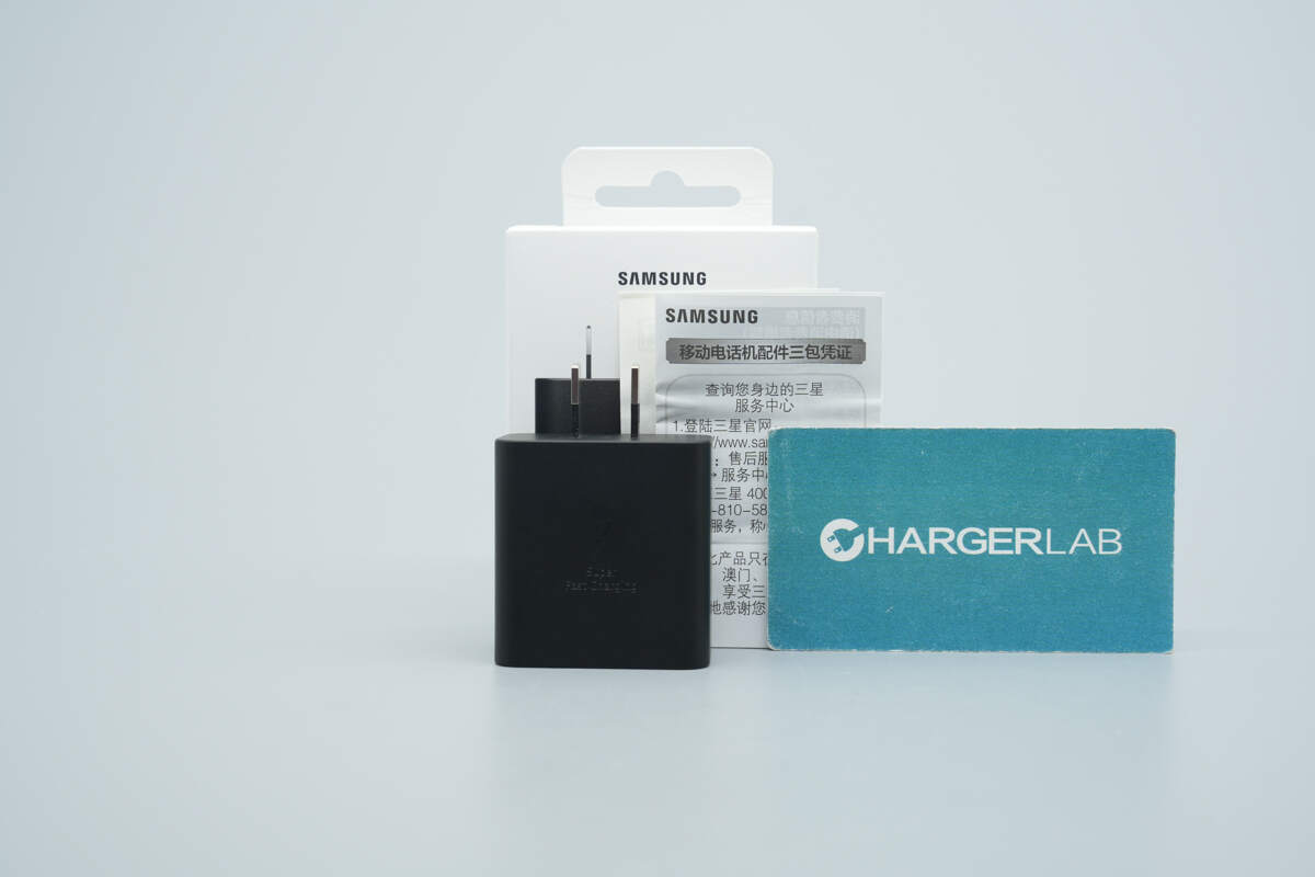
The package includes the charger, the warranty certificate, and a list of hazardous substances.
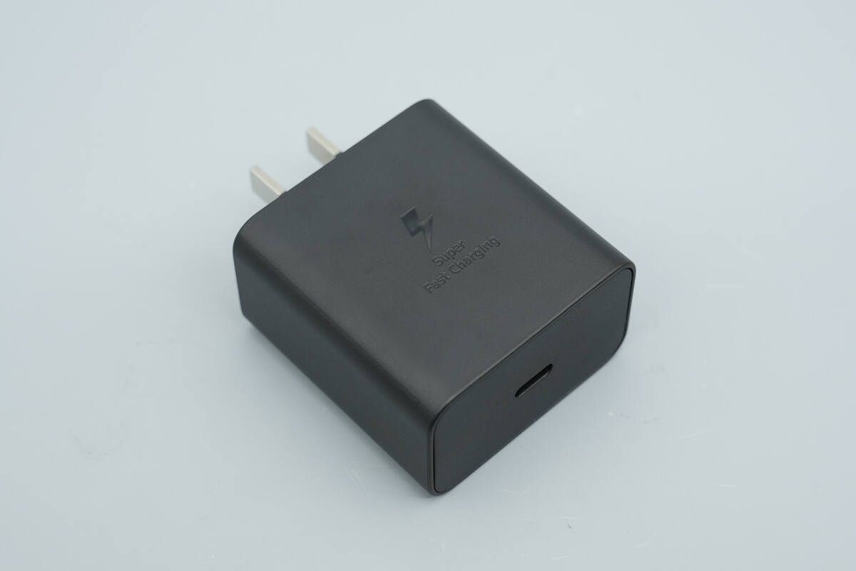
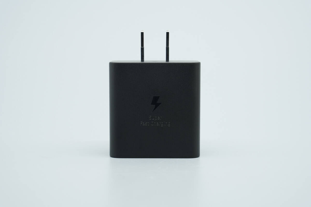
The charger is entirely black with a matte finish.
The center of the front features a lightning logo and the text “SuperFast Charging.”
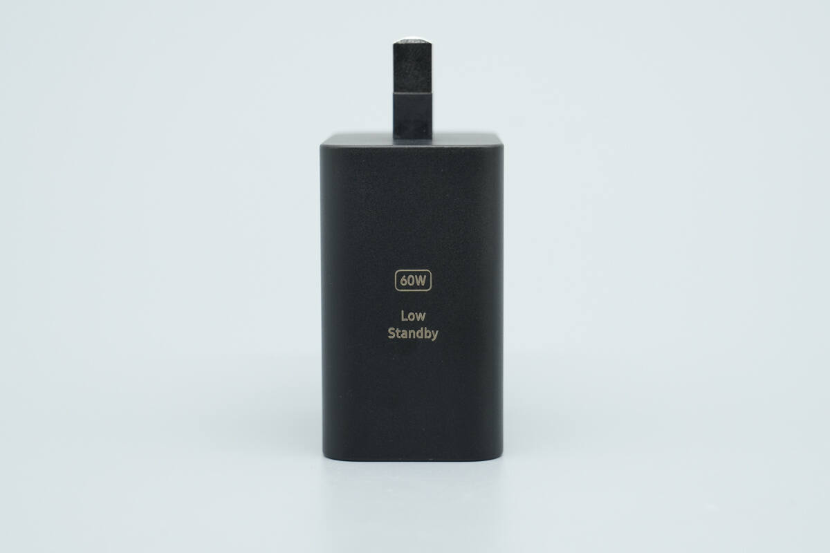
The side displays “60W” and “Low Standby.”
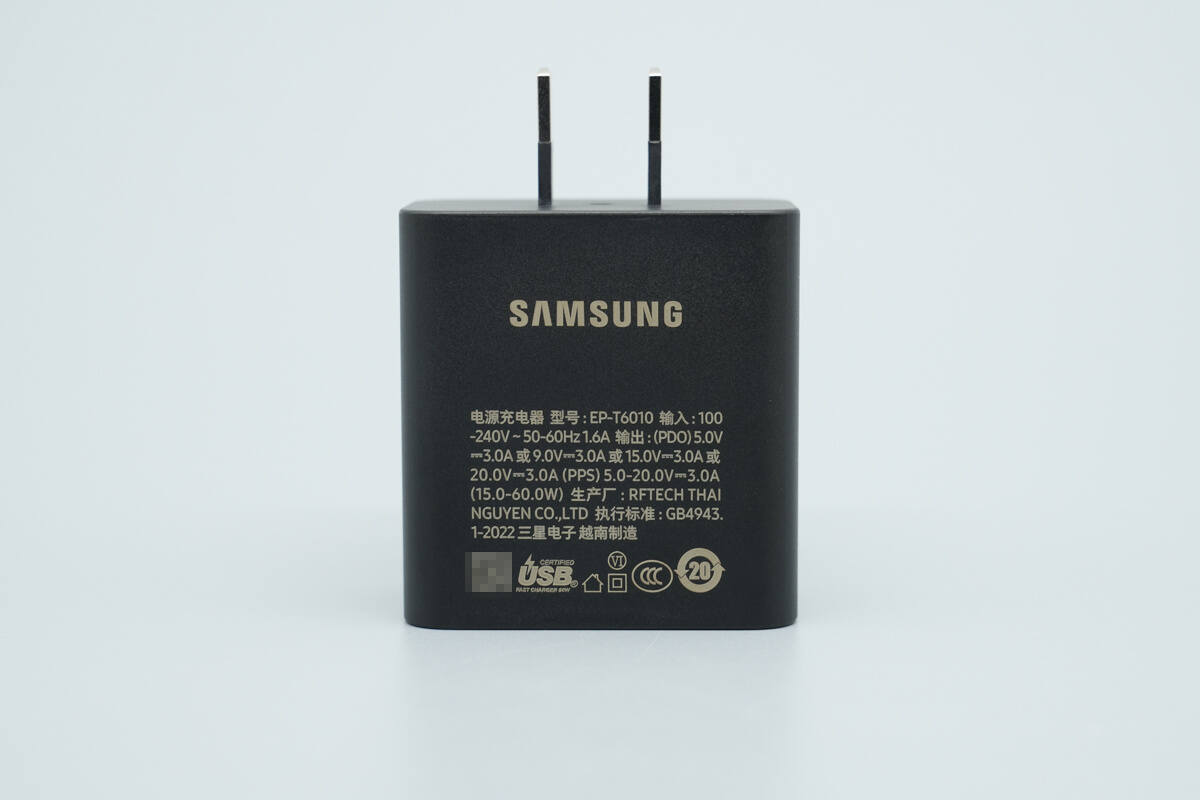
The back displays the charger’s technical specifications.
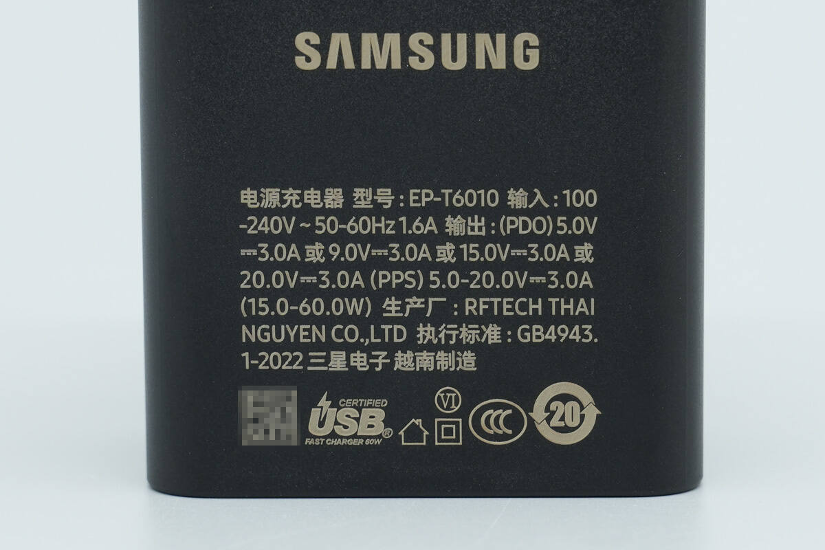
Model: EP-T6010
Input: 100-240V~ 50/60Hz 1.6A
Output: (PDO) 5V 3A, 9V 3A, 15V 3A, 20V 3A
(PPS) 5-20V 3A (15-60W)
Manufacturer: RFTECH THAINGUYEN CO., LTD
The charger is certified with CCC and Level VI energy efficiency.
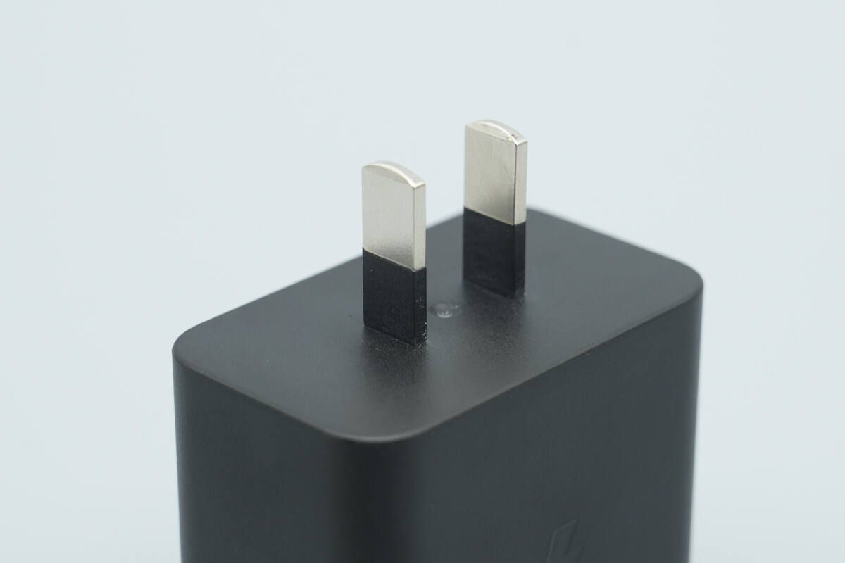
The charger is equipped with fixed prongs.
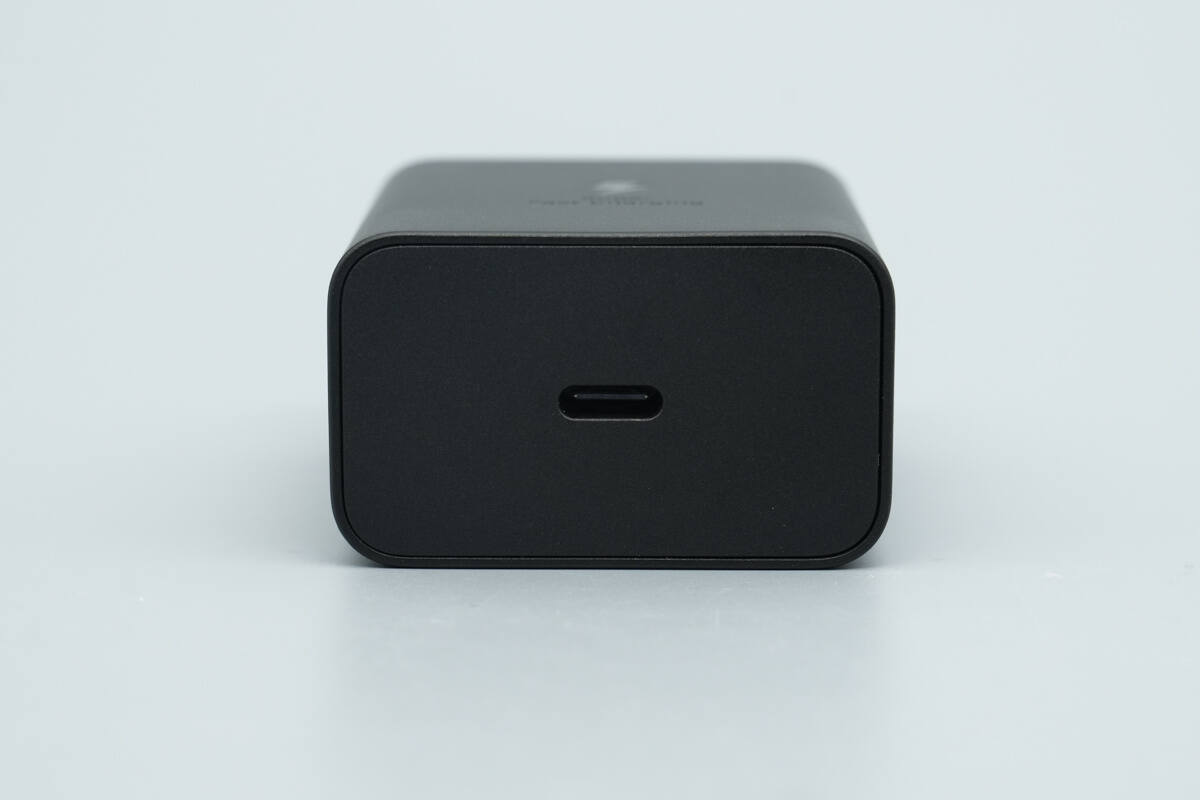
The top is equipped with a single USB-C port.
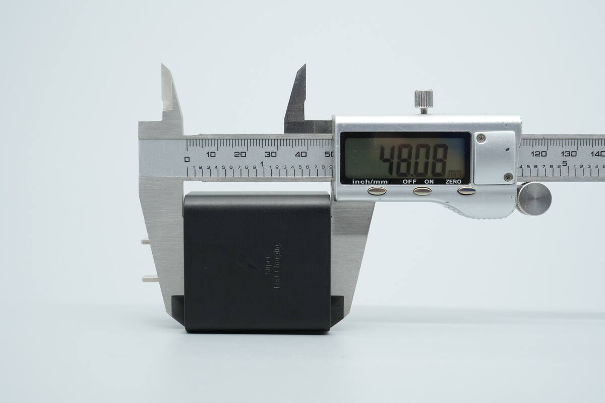
The length of the charger is about 48.08 mm (1.89 inches).
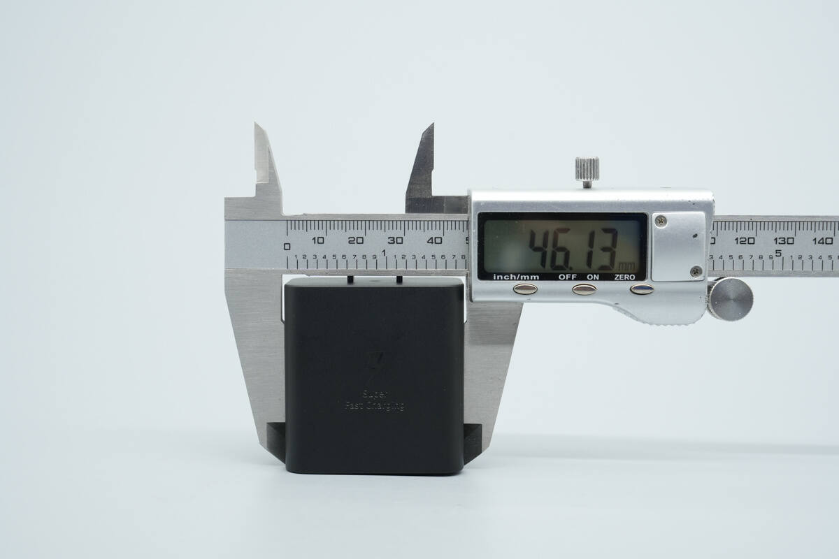
The width is about 46.13 mm (1.82 inches).
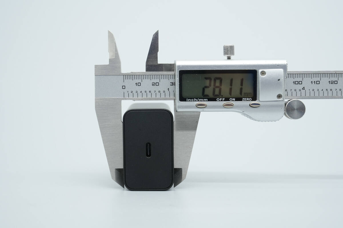
The thickness is about 28.11 mm (1.11 inches).
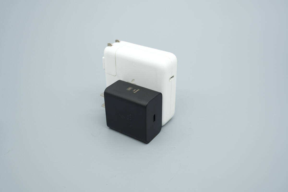
Compared with the Apple 67W charger, it has a clear size advantage.
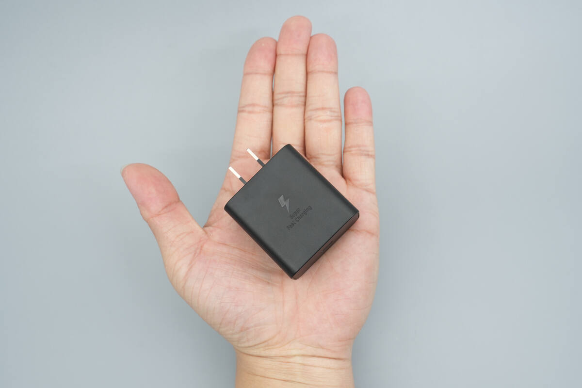
That's how big it is in the hand.
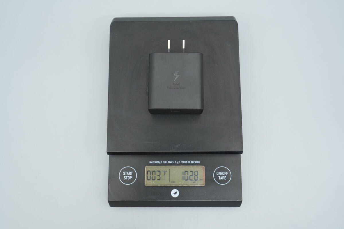
The weight is about 103 g (3.63 oz).
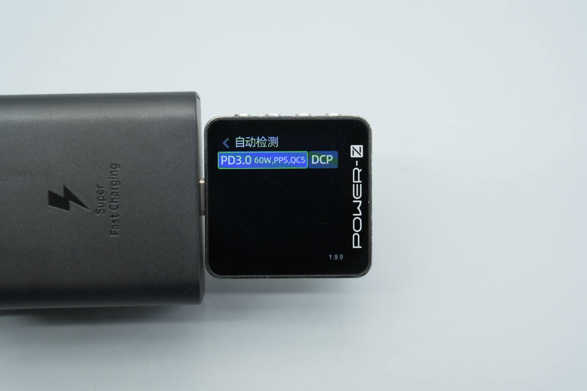
ChargerLAB POWER-Z KM003C shows that it supports PD3.0, PPS, QC5, and DCP charging protocols.
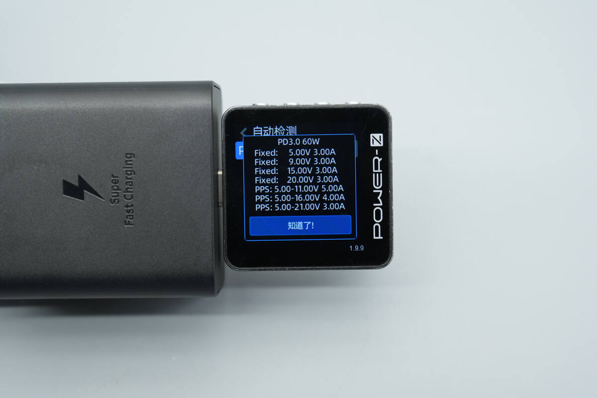
It has four fixed PDOs of 5V3A, 9V3A, 15V3A, and 20V3A. It also has three sets of PPS, which are 5-11V5A, 5-16V4A, and 5-21V3A.
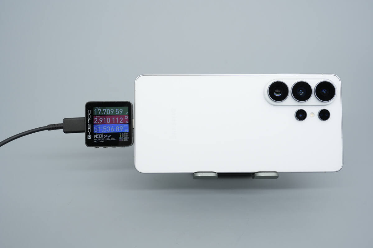
When used to charge the Galaxy S26 Ultra, the charging power is about 51.54W.
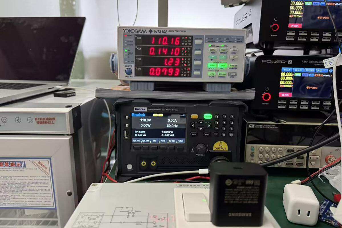
At a 110V input, its no-load standby power consumption is 1.23 mW.
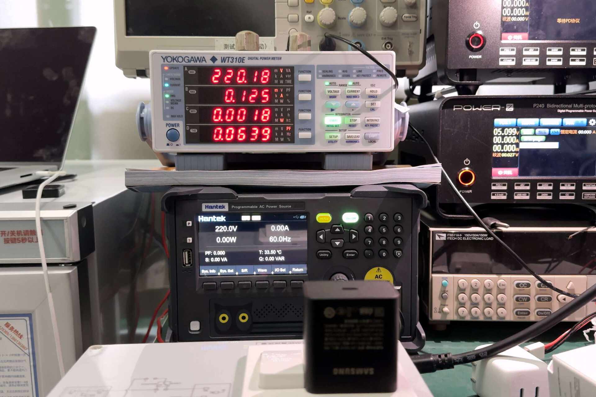
At a 220V input, its no-load standby power consumption is 1.8 mW (calculated from 0.0018 W).
According to the IEC62301 standard, a power consumption of less than 5 mW qualifies as zero standby. The measured data of this Samsung charger, designed based on the BPS BP87650A + BP62650A power solution, fully meet this standard.
Teardown
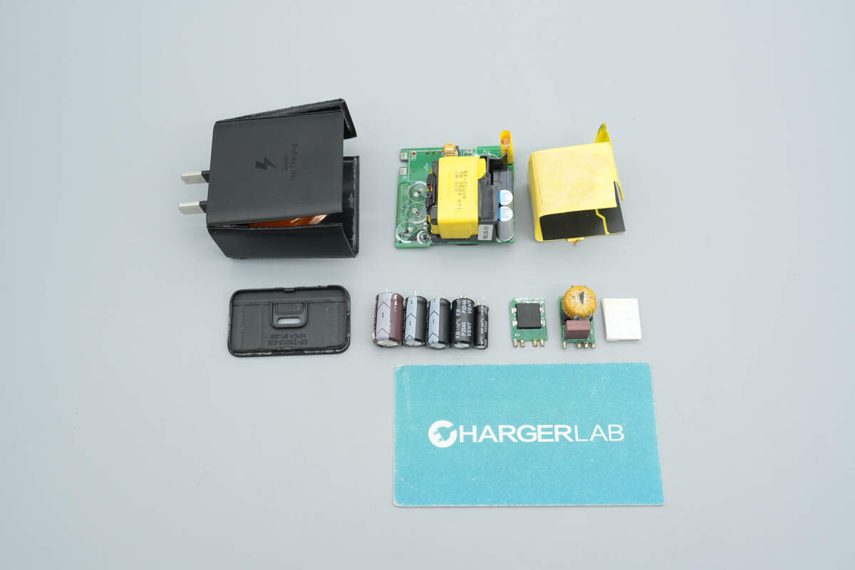
Next, let's take it apart to see its internal components and structure.
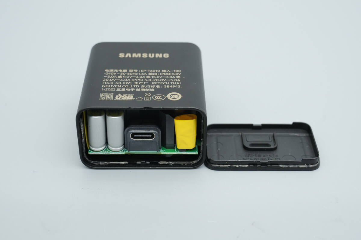
The top casing, which features ultrasonically welded edges, is removed.
The casing is cut open to remove the PCBA module.
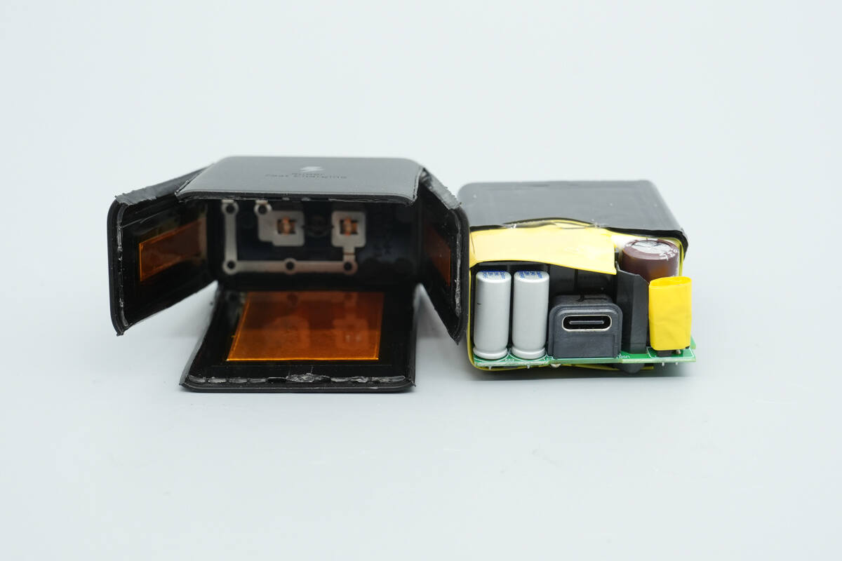
The inner side of the casing is designed for insulation and heat dissipation.
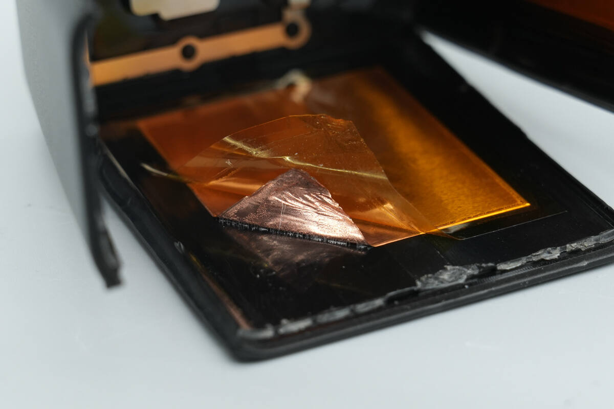
The inner side is lined with copper foil and high-temperature resistant insulating tape.
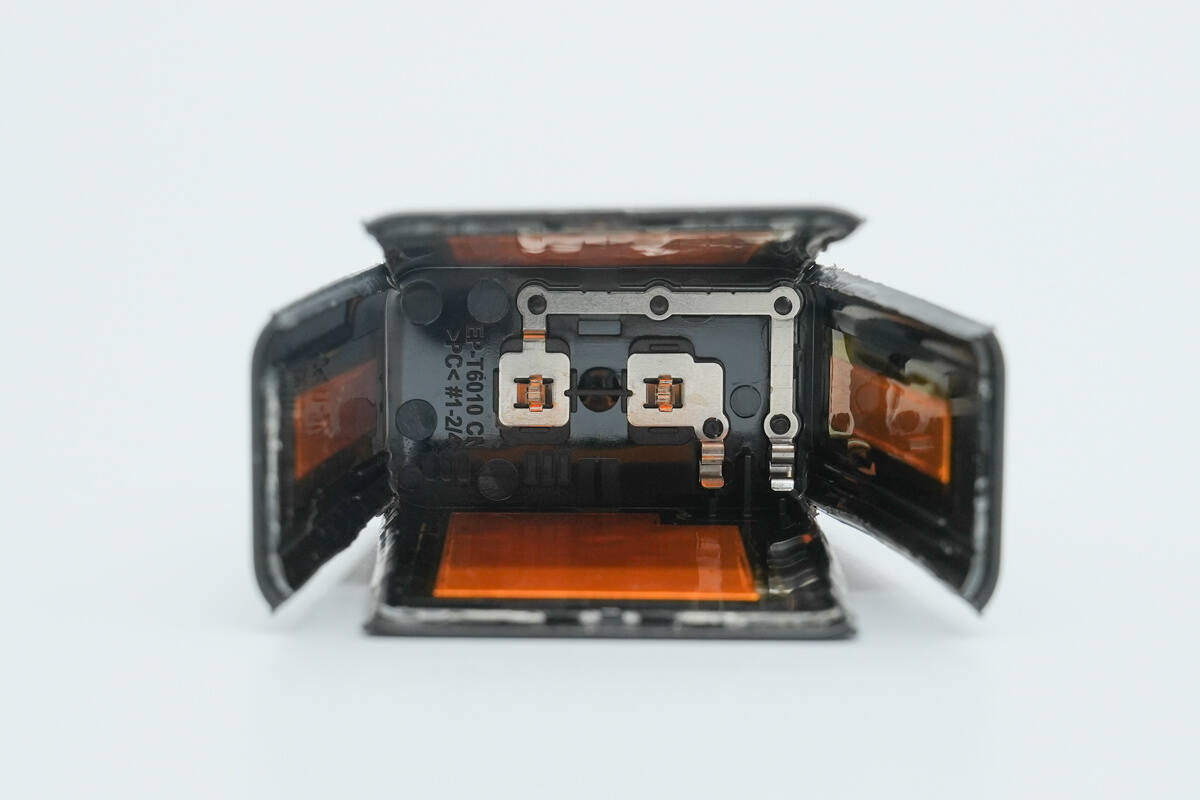
The input end uses a contact-type power connection design, with the prongs crimped to metal plates.
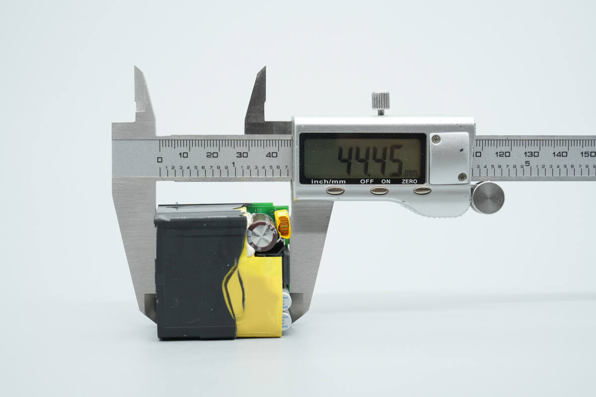
The length of the PCBA module is about 44.45 mm (1.75 inches).
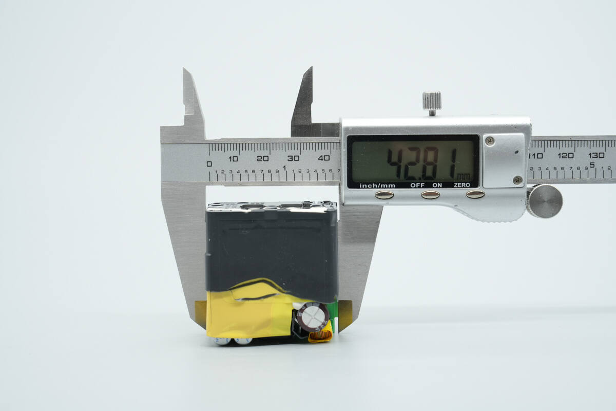
The width is about 42.81 mm (1.69 inches).
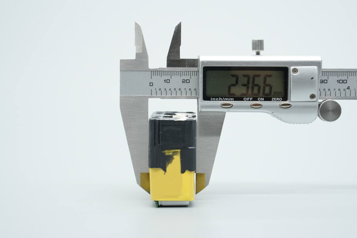
The thickness is about 23.66 mm (0.93 inches).
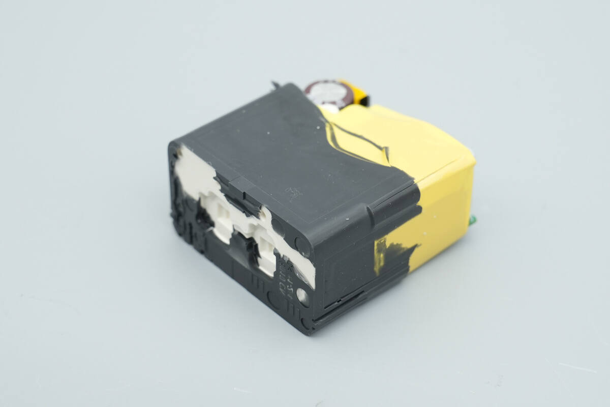
The PCBA module is encased in a copper sheet.
The thermal adhesive and copper sheets are removed. A Mylar sheet is also attached to the back of the PCBA.
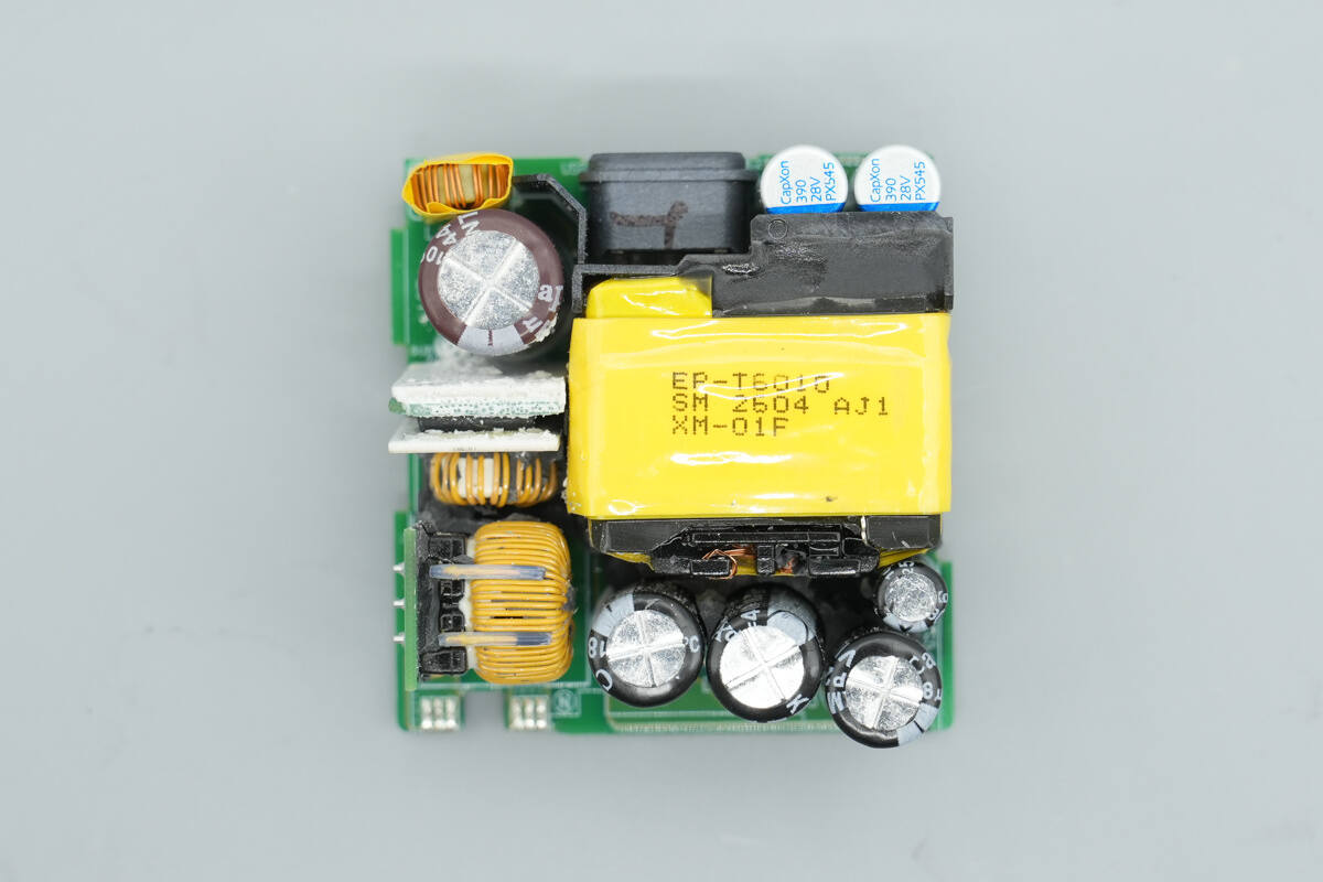
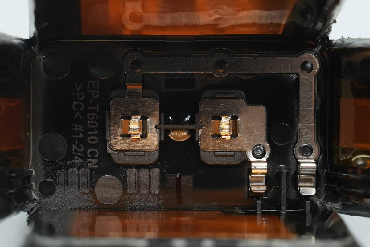
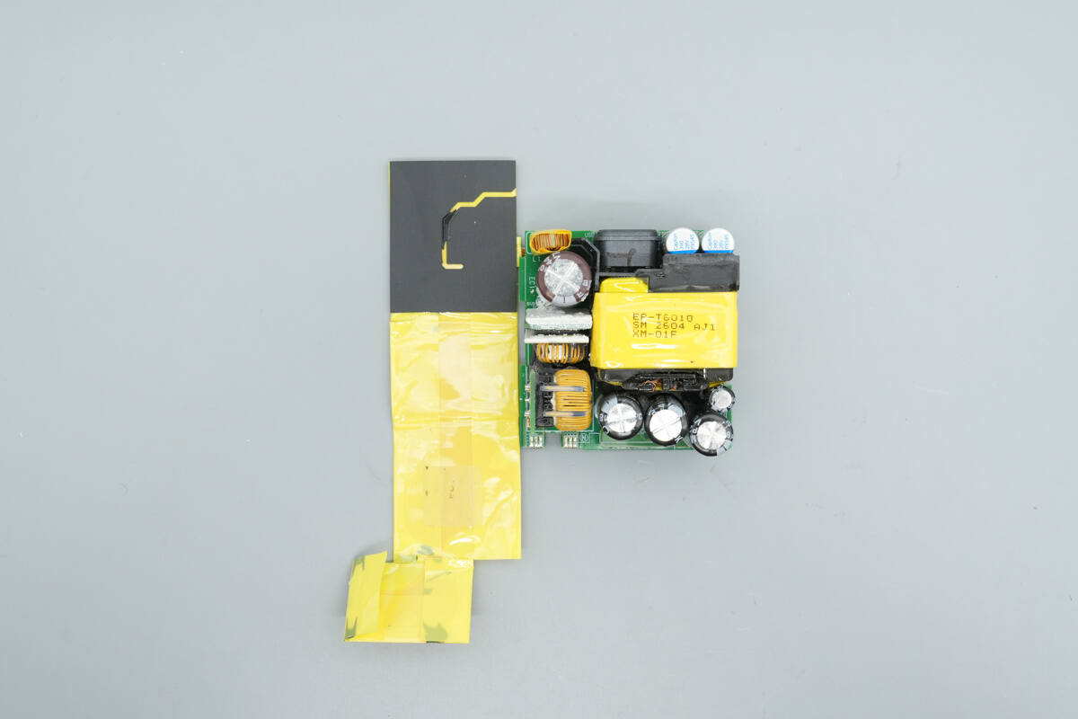
The front of the PCBA module contains common mode chokes, filter capacitors, transformers, and other components.
The back of the PCBA features the primary master control chip, magnetic couplers, SMD Y capacitors, and the protocol chip.
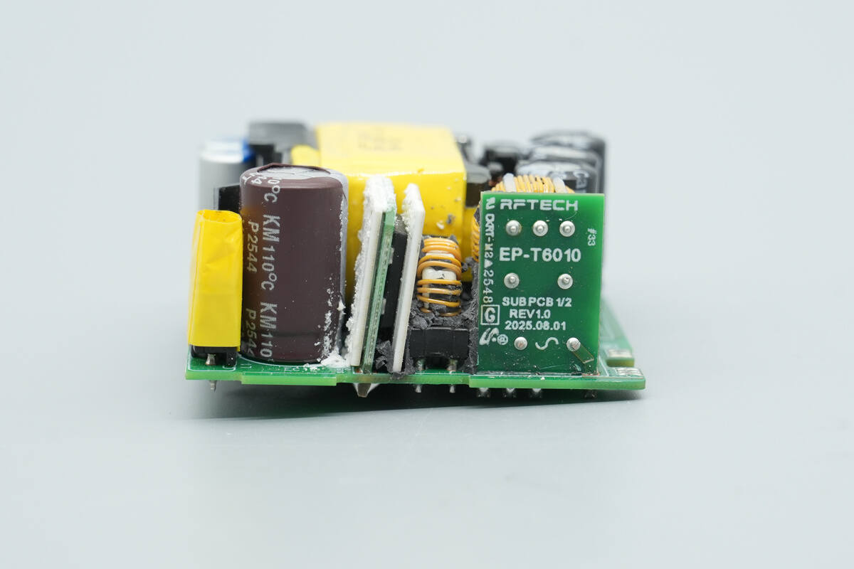
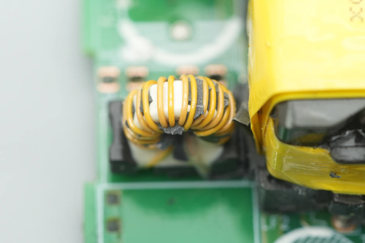
This side contains the input PCB, rectification PCB, a high-voltage filter electrolytic capacitor, and a differential mode choke.
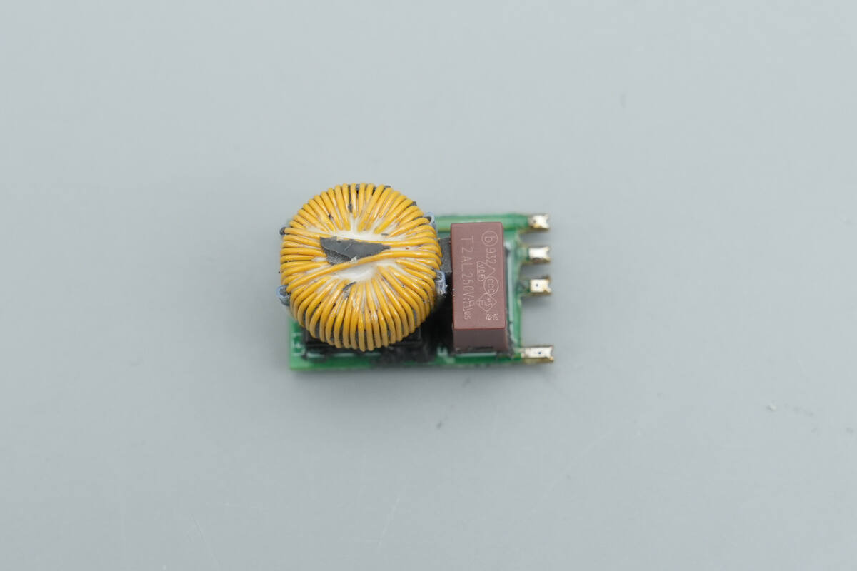
The front of the input PCB is equipped with a time-delay fuse and a common mode choke.
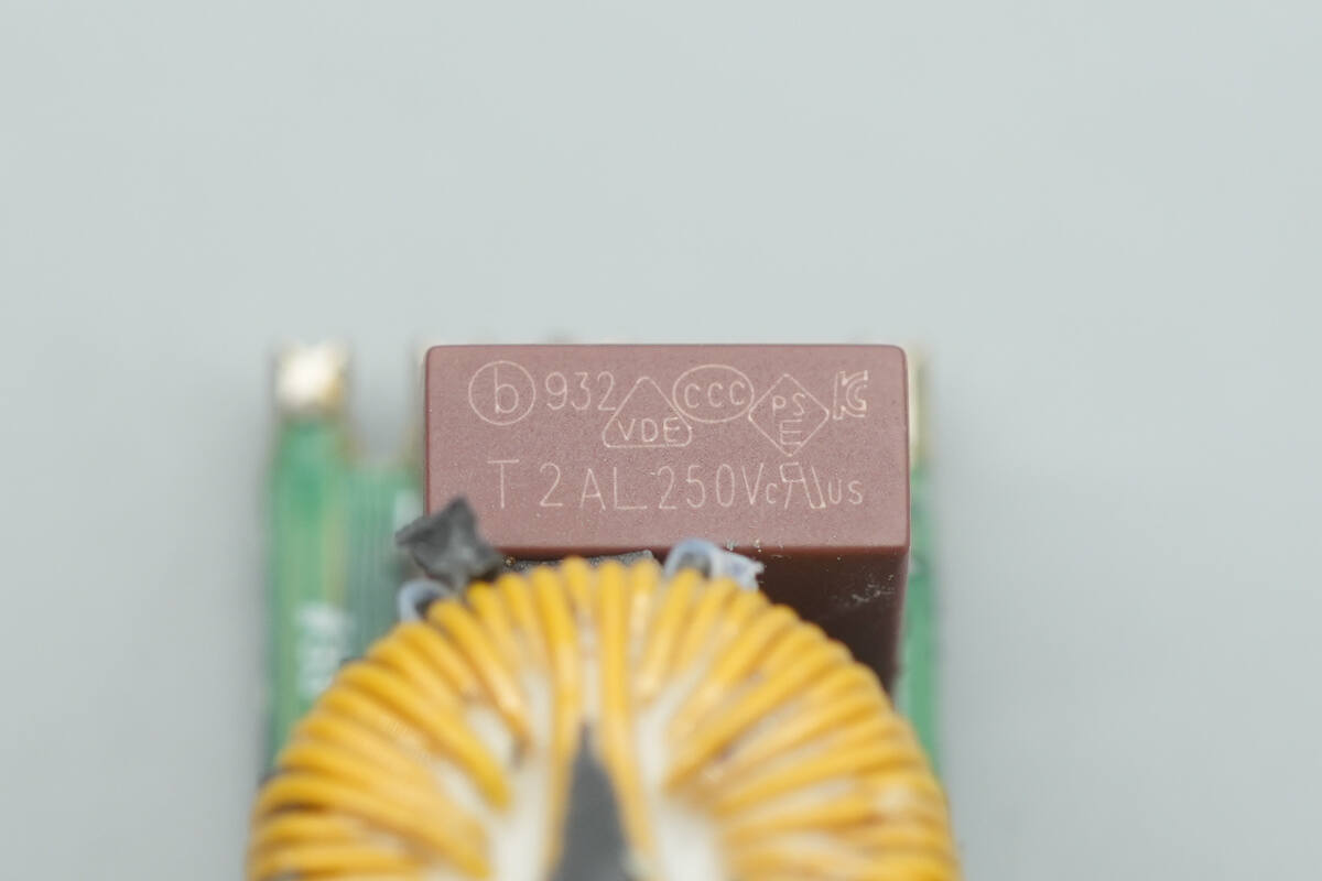
The time-delay fuse is from Betterfuse, part number 932, rated at 2 A 250 V.
The common mode choke is reinforced with adhesive.
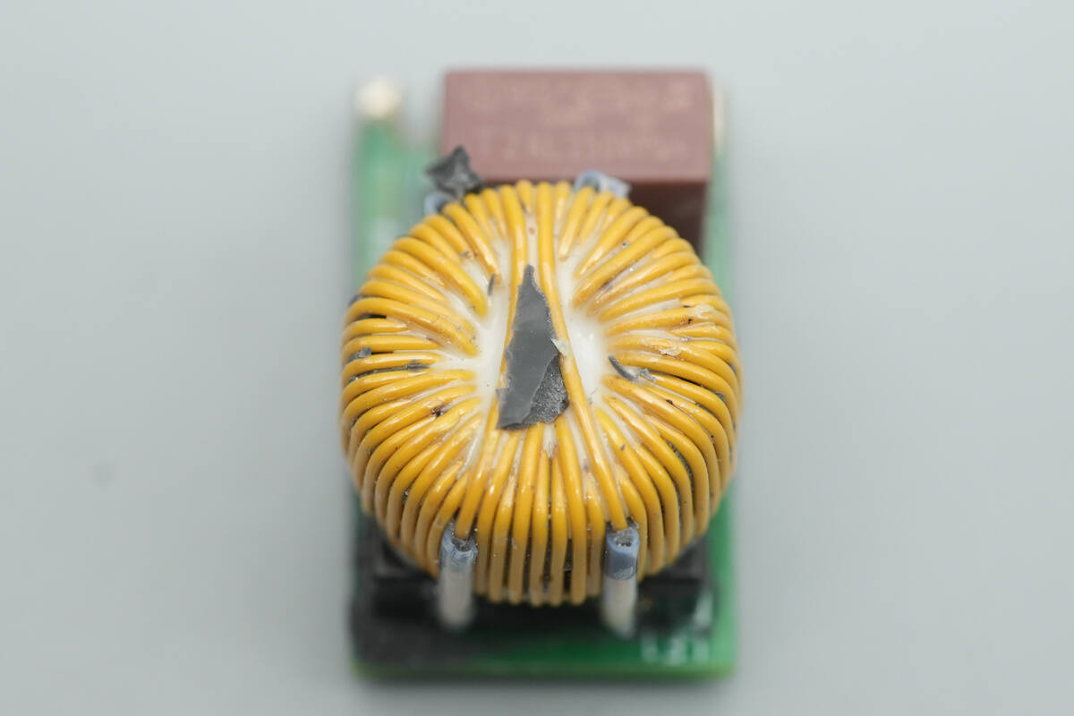
A close-up view of the other common mode choke.
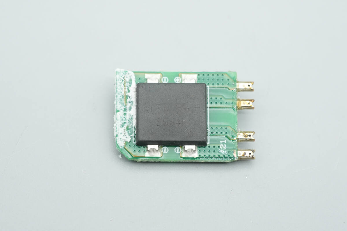
The bridge rectifier is model RULBF810T.
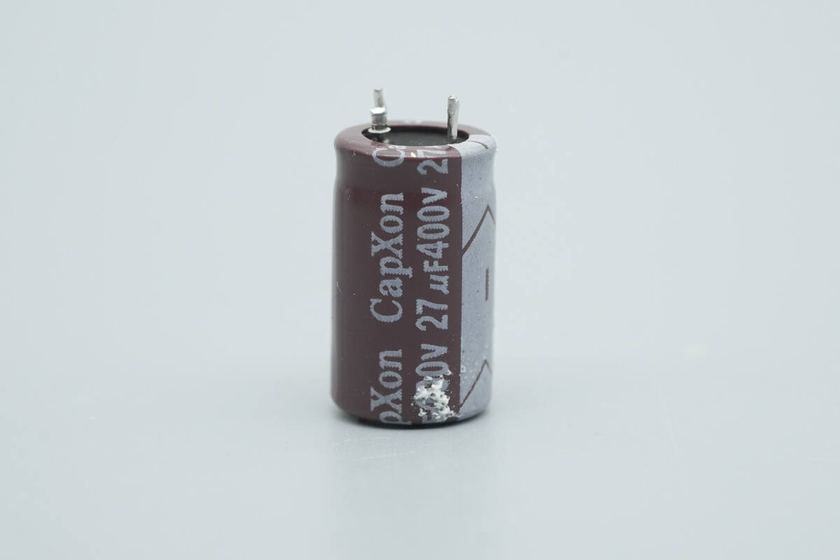
The high-voltage filter electrolytic capacitor is from CapXon, rated at 400 V, 27 μF.
The differential-mode choke is wrapped with insulating tape.
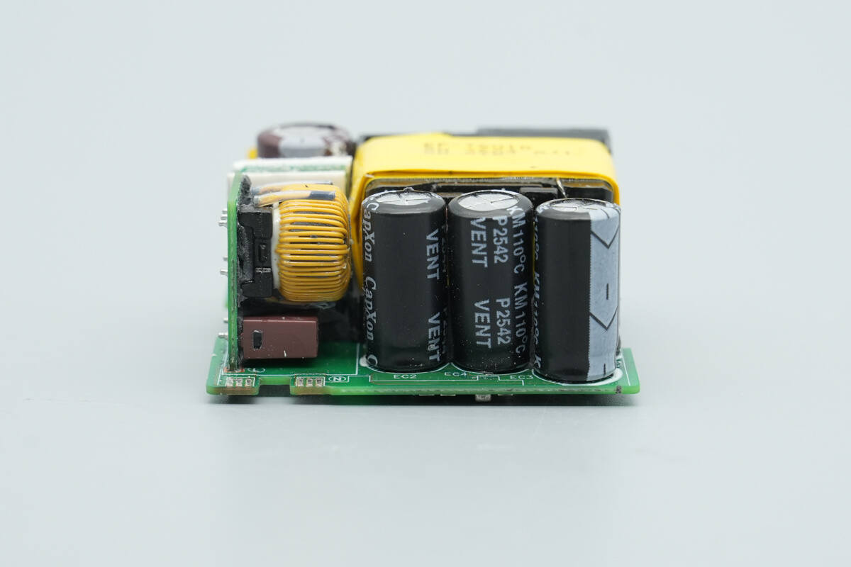
The front end of the module is equipped with three additional high-voltage filter electrolytic capacitors.
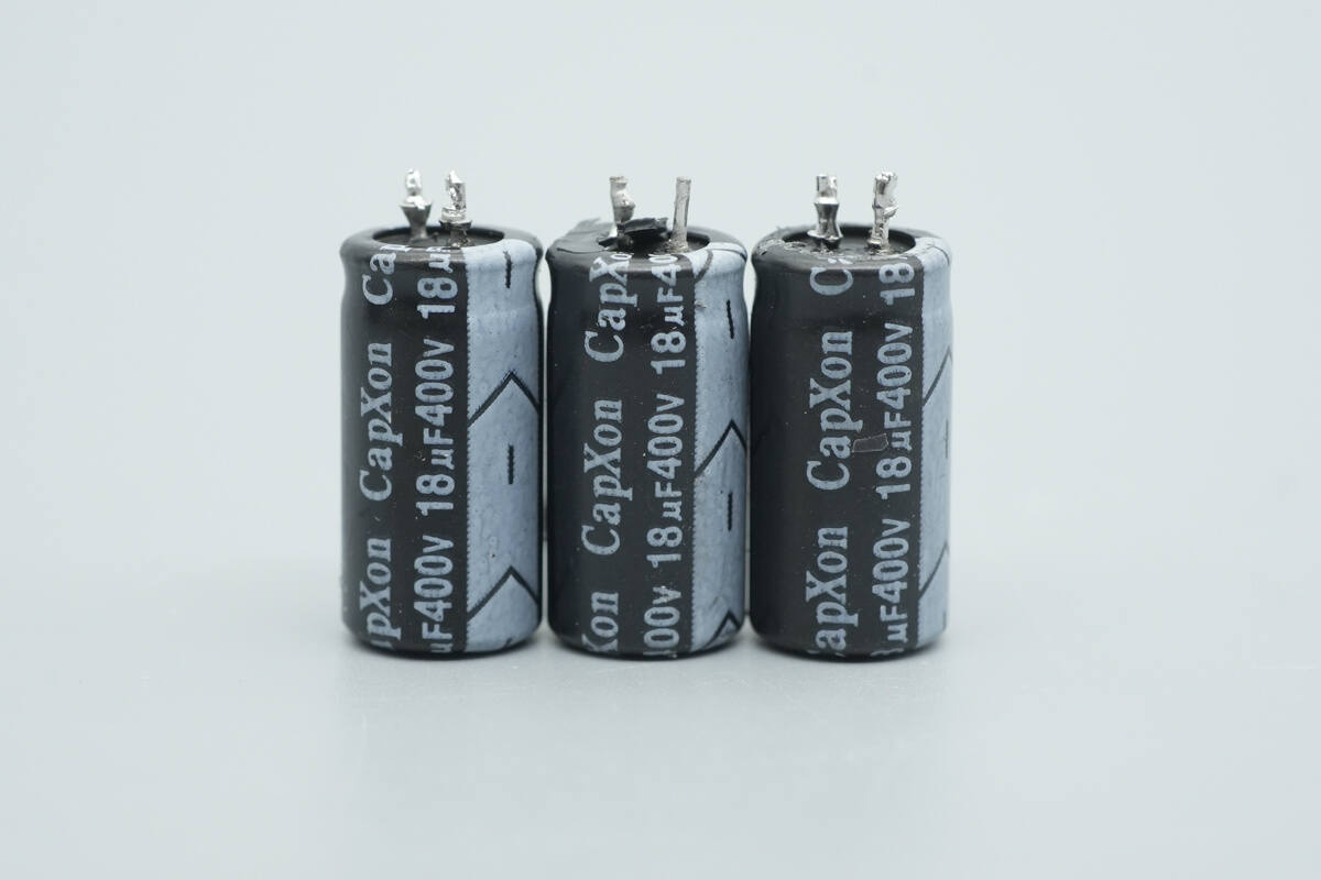
The three high-voltage filter electrolytic capacitors are also from CapXon, each rated at 400 V, 18 μF.
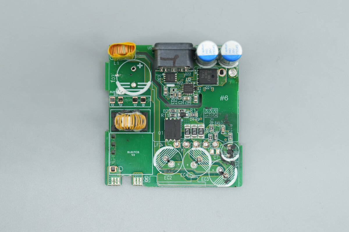
After removing the capacitors, transformer, and other components, the area beneath the transformer reveals a GaN FET, a secondary controller, a synchronous rectifier, and a VBUS MOSFET.
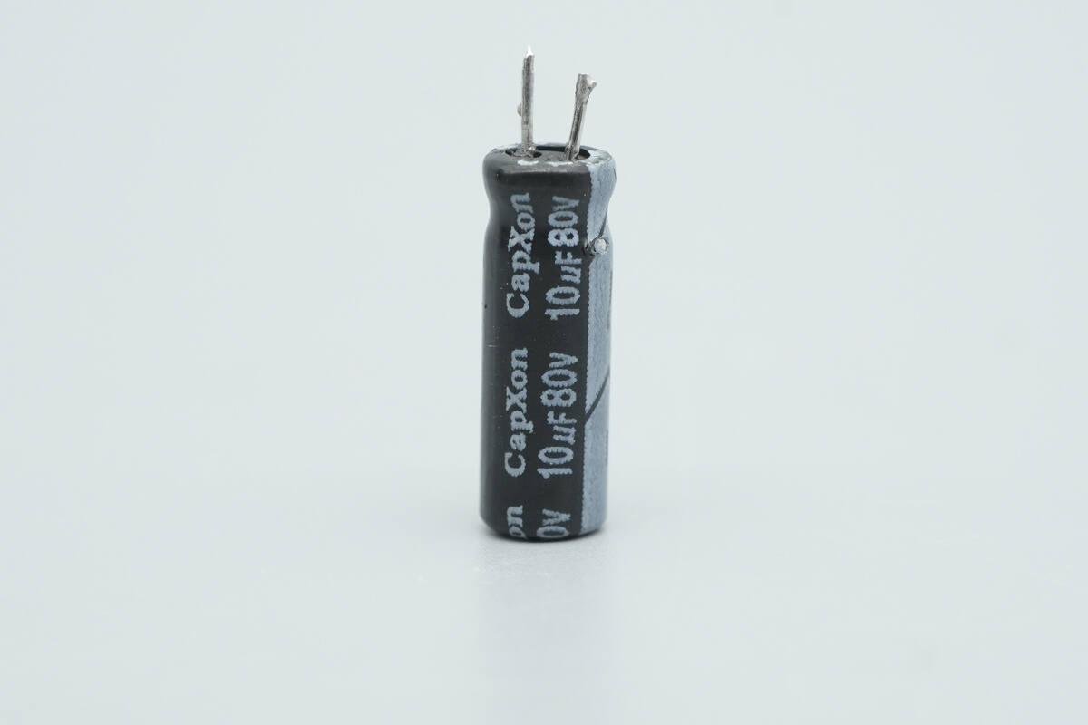
The capacitor supplying power to the master control chip is from CapXon, rated at 80 V, 10 μF.
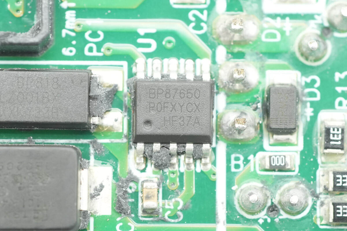
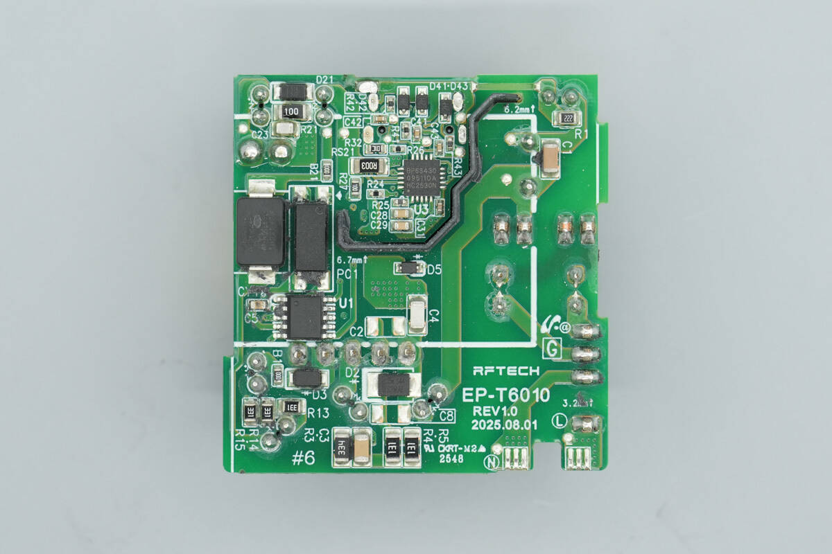
The primary master control chip is from BPS, model BP87650A. It is a high-performance quasi-resonant flyback controller that enables zero no-load power consumption in fast charger applications. The chip communicates with the secondary-side controller BP62650A via the magnetic coupler BP818 to achieve secondary-side regulation. Because the magnetic coupler operates without a bias current, the system’s no-load power consumption is significantly reduced to below 5 mW.
The BP87650A operates in conventional QR/DCM mode and employs valley switching technology to achieve high efficiency and excellent EMI performance. It integrates an enhanced GaN power transistor gate driver, a 700 V high-voltage startup current source, and an auxiliary power supply module supporting up to 150 V input. Its high level of integration greatly reduces the number of external components and lowers system cost, making it an ideal choice for compact travel adapter applications.
The BP87650A also provides comprehensive protection features to safeguard the system under abnormal conditions. The chip comes in an SSOP-10 package and meets the MSL-3 moisture sensitivity level standard.
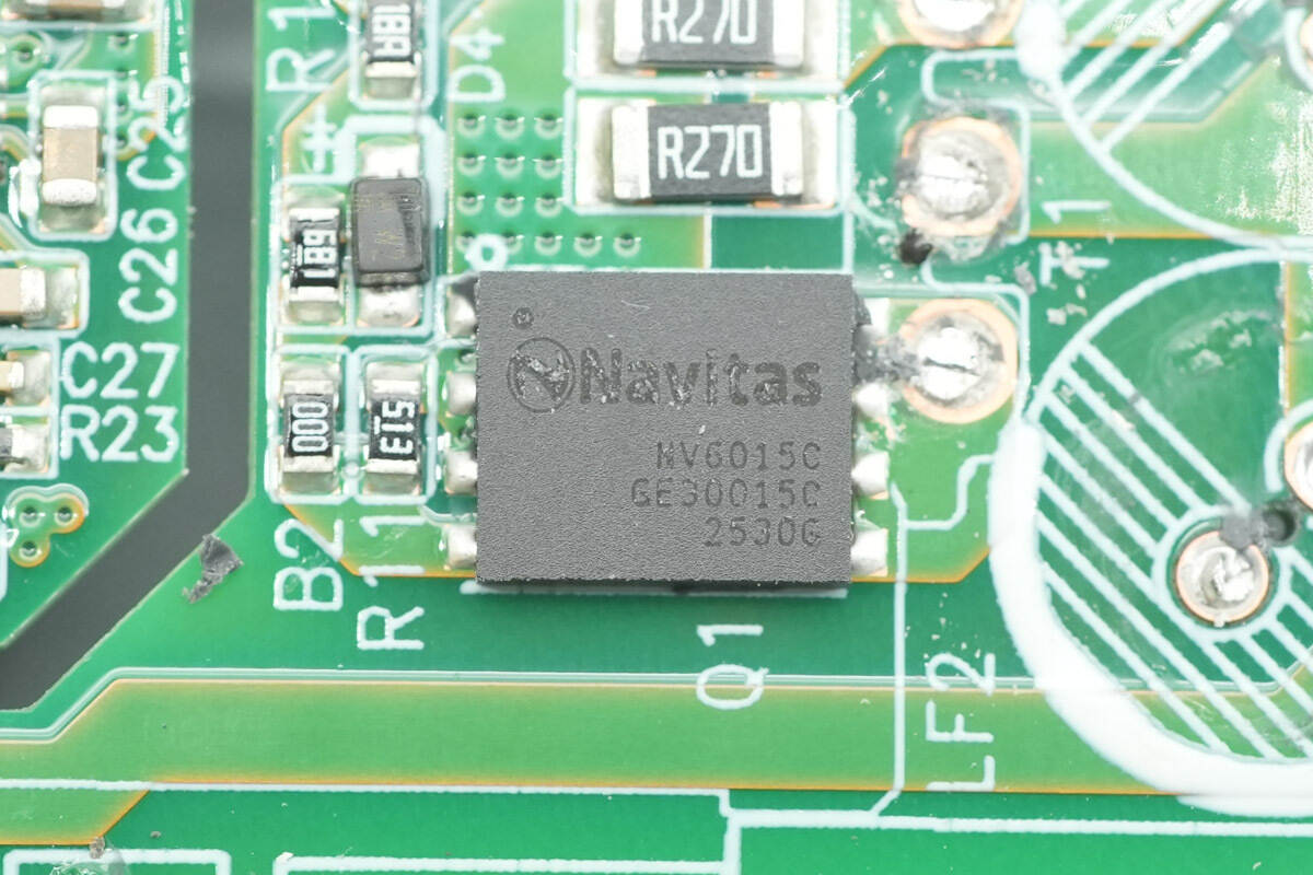
The GaN FET is from Navitas, model NV6015C. It is a high-performance enhancement-mode GaN FET with an integrated Source Kelvin pin to improve noise immunity. It comes in a 5×6 mm QFN package with bottom-side thermal pad, effectively reducing thermal resistance and package inductance while saving PCB space.
The NV6015C features an on-resistance of 150 mΩ, a voltage rating of 700 V (supporting 800 V transient overvoltage), and a switching frequency of up to 10 MHz. It has ultra-low gate charge, zero reverse-recovery charge, and low output charge, significantly reducing switching losses.
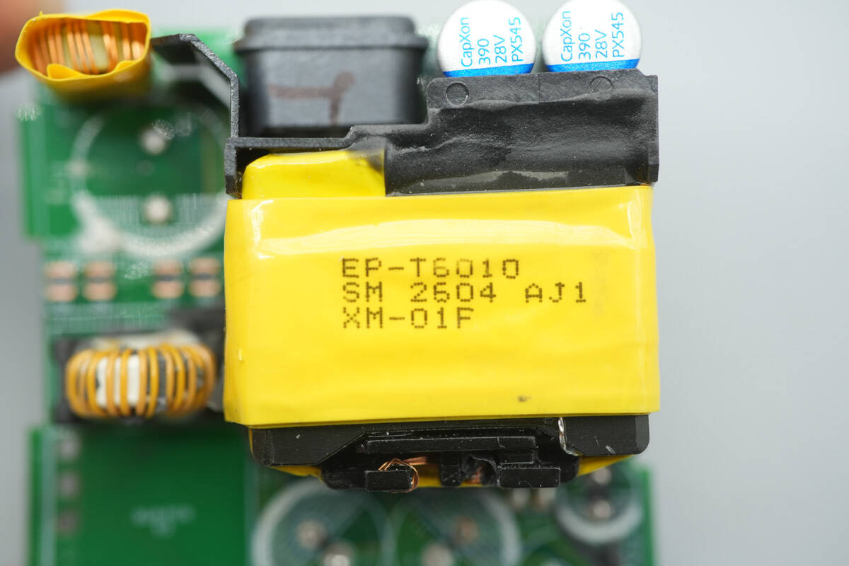
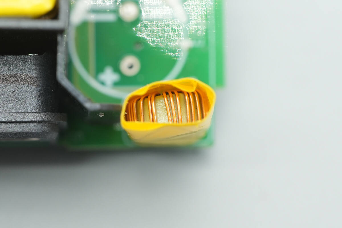
A close-up view of the transformer.
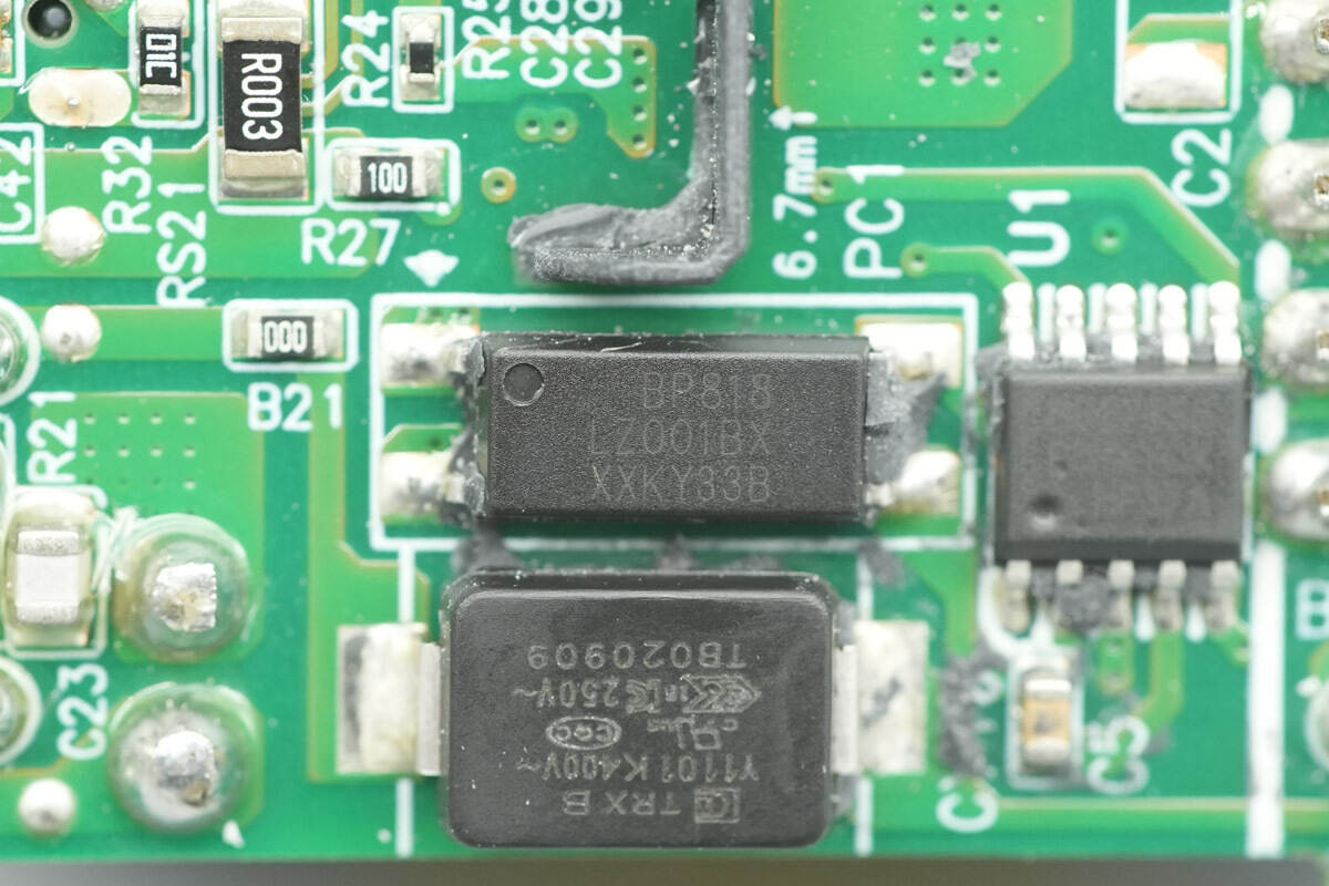
The BPS patented magnetic-coupled communication feedback component BP818, which resembles an optocoupler in appearance, has obtained global safety certifications. The device integrates two coupling coils for primary-to-secondary communication, operating without a bias current, effectively reducing standby power consumption.
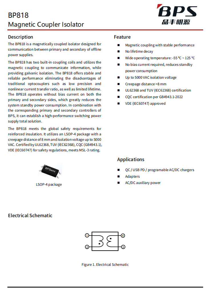
Here is the information about BPS BP818.
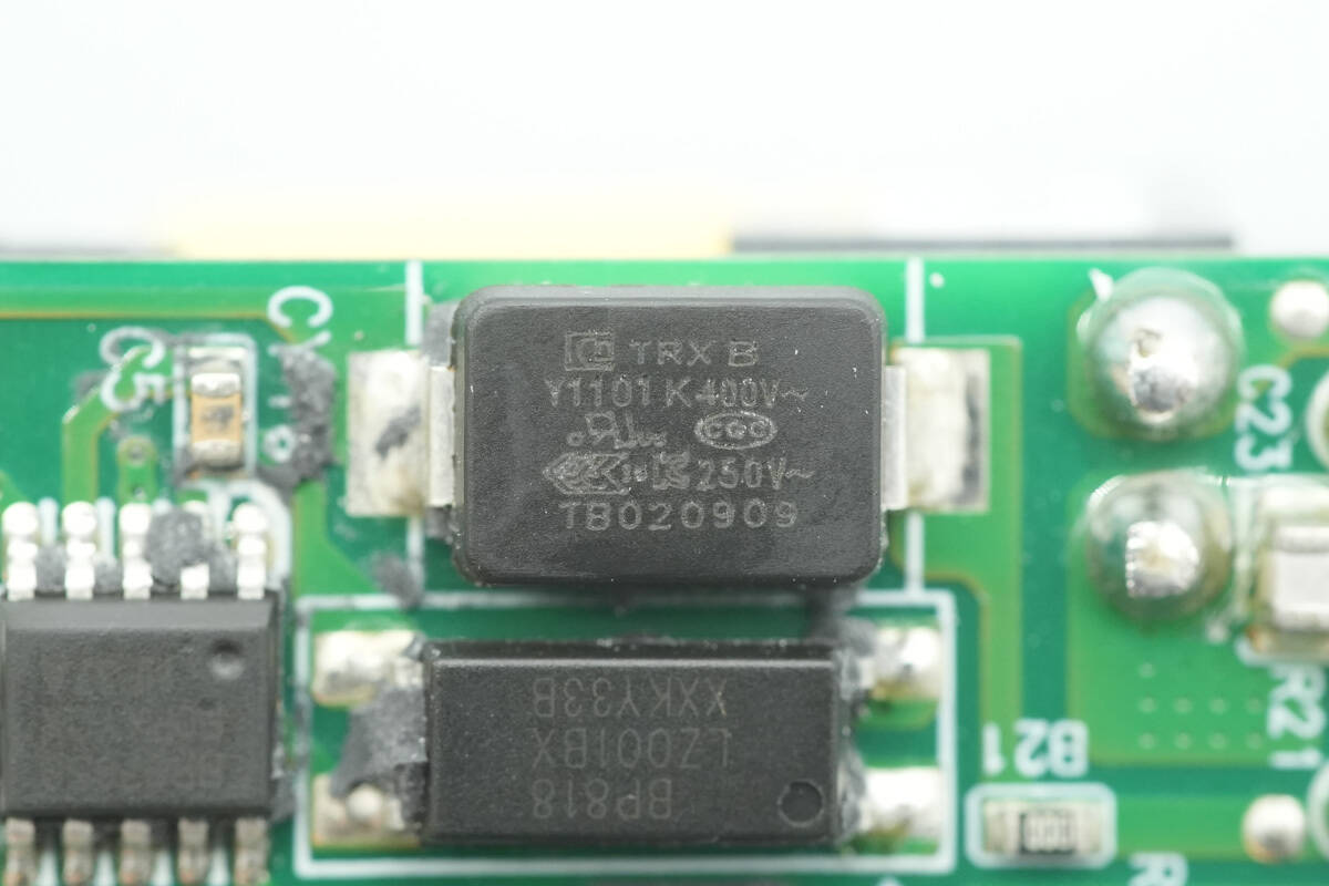
The SMD Y capacitor is from TRX, part number TMY1101K. Its compact size and light weight make it well-suited for high-density power products such as GaN fast chargers.
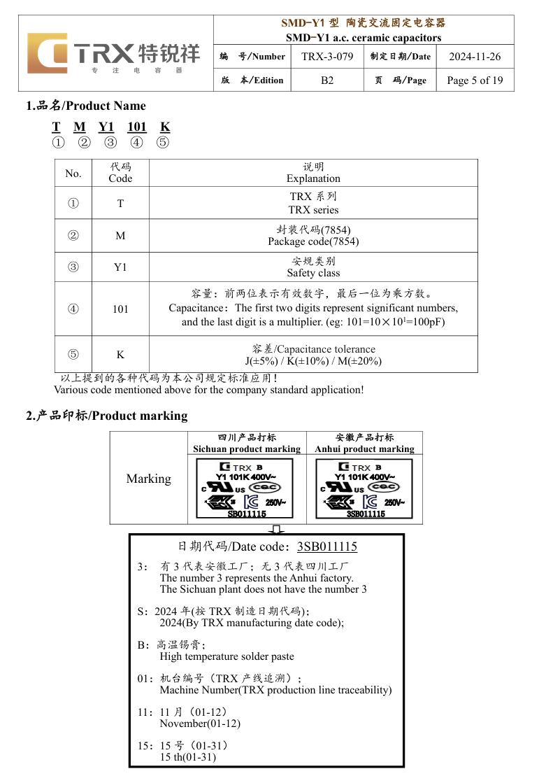
Here is the information about the TRX SMD Y capacitor.
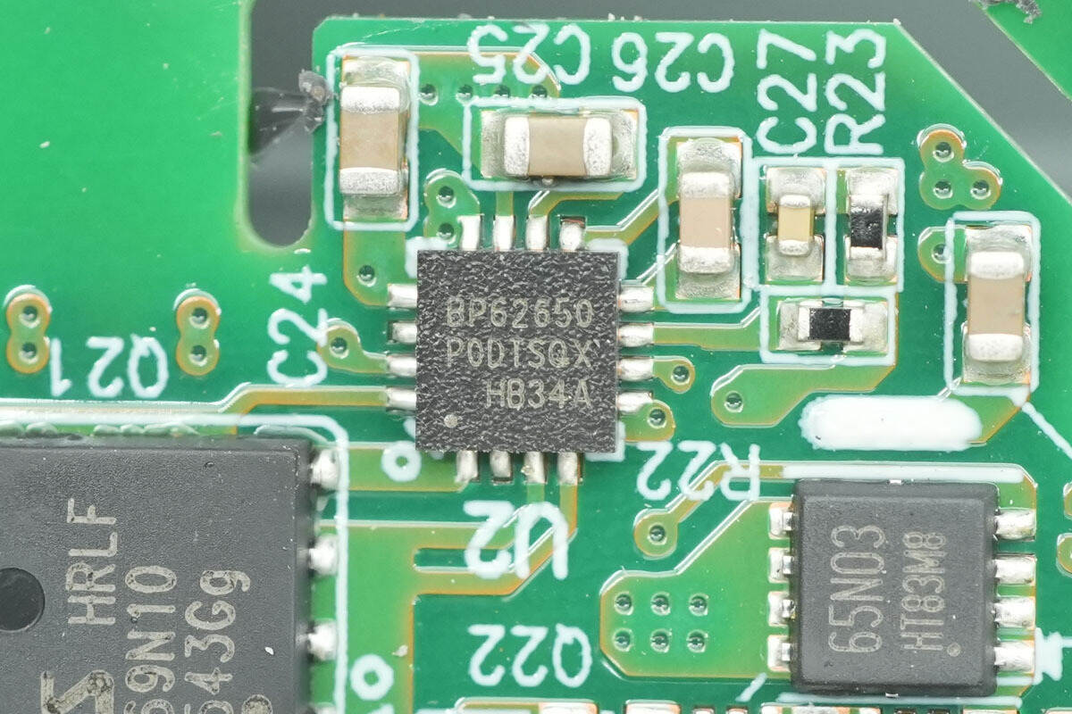
The BPS BP62650A is an AC/DC secondary-side controller. When used in conjunction with the BP87650A, it enables zero standby power consumption in travel adapter applications. The chip employs a control algorithm based on output voltage ripple, achieving fast transient response without requiring complex loop compensation circuits.
The BP62650A sends request signals to the primary-side controller via the magnetic coupler BP818 to regulate the output voltage. In standby mode, it can enter an ultra-low-power sleep state under control, resulting in extremely low secondary-side power consumption. This eliminates losses from the feedback resistor network, and since the magnetic coupler requires no bias current, the overall system power consumption is well below 5 mW.
The BP62650A integrates an advanced synchronous rectification controller to optimize drive duty cycle and improve system efficiency. Powered by a charge pump, its output voltage can go as low as 2.8 V. The chip comes in a QFN 3×3-16L package and meets the MSL-3 moisture sensitivity level standard.
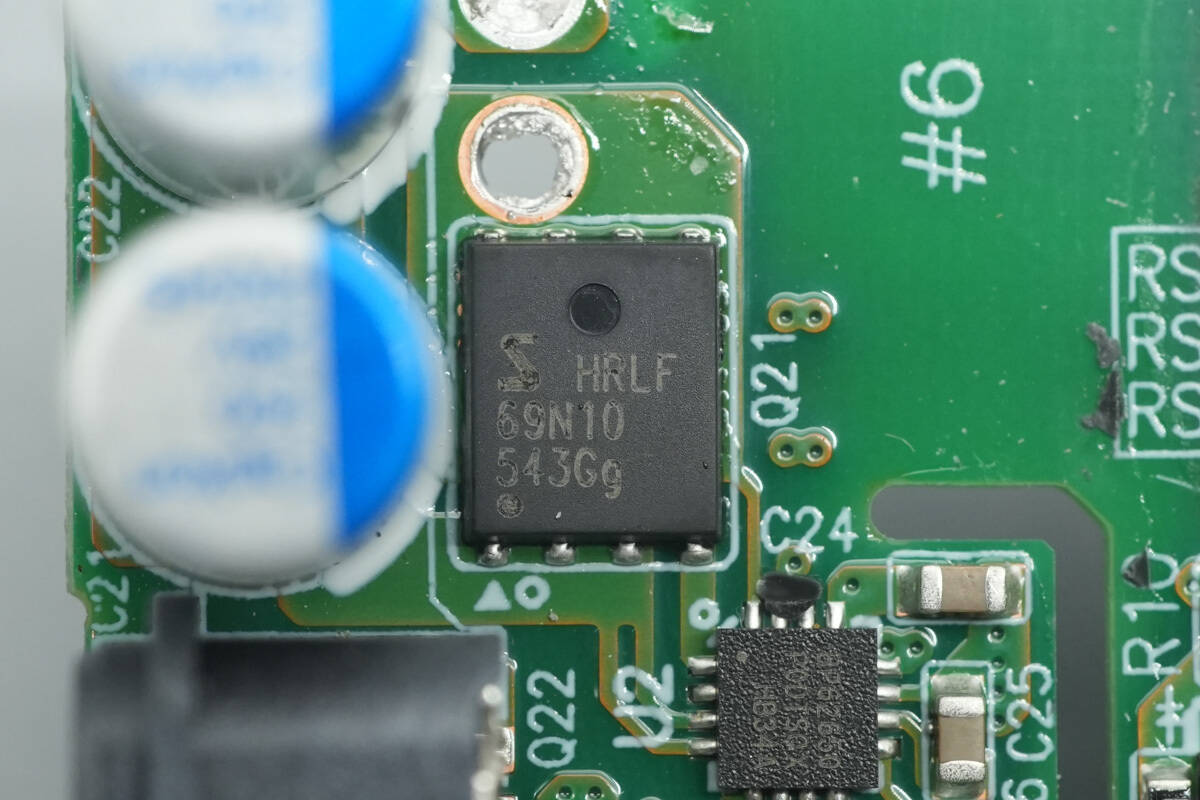
The synchronous rectifier is from SemiHow, model HRLF69N10, and comes in a 5×6 mm DFN package.
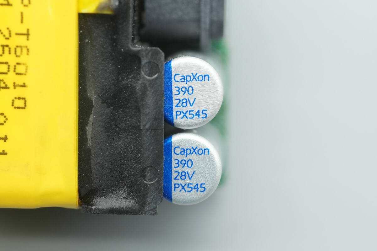
The two output filter solid capacitors are also from CapXon, each rated at 28 V, 390 μF.
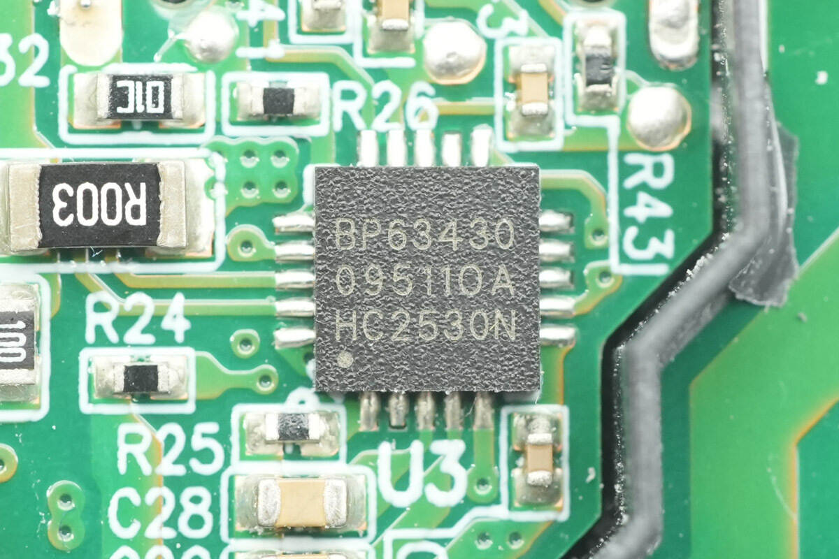
The protocol chip is from BPS, model BP63430N. It is a highly integrated Type-C/PD and DPDM fast-charging source-side controller, compliant with the latest USB Type-C and PD 3.1 standards. It supports mainstream fast-charging protocols, including BC1.2, QC5/4+/3+/3.0/2.0, UFCS, and also allows for proprietary protocol customization. This makes it suitable for applications such as power adapters, wall chargers, and car chargers.
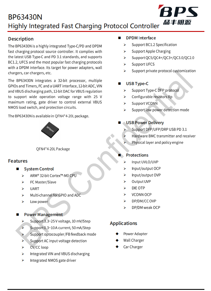
The BP63430N integrates a 32-bit processor, multiple GPIOs and timers, I2C and UART interfaces, a 12-bit ADC, VIN and VBUS discharge paths, and a 12-bit DAC for VBUS regulation to support a wide operating voltage range (maximum rated 25 V). It also includes a gate driver for controlling external VBUS N-MOS load switches and built-in protection circuits. The chip comes in a 4×4 mm QFN-20L package.
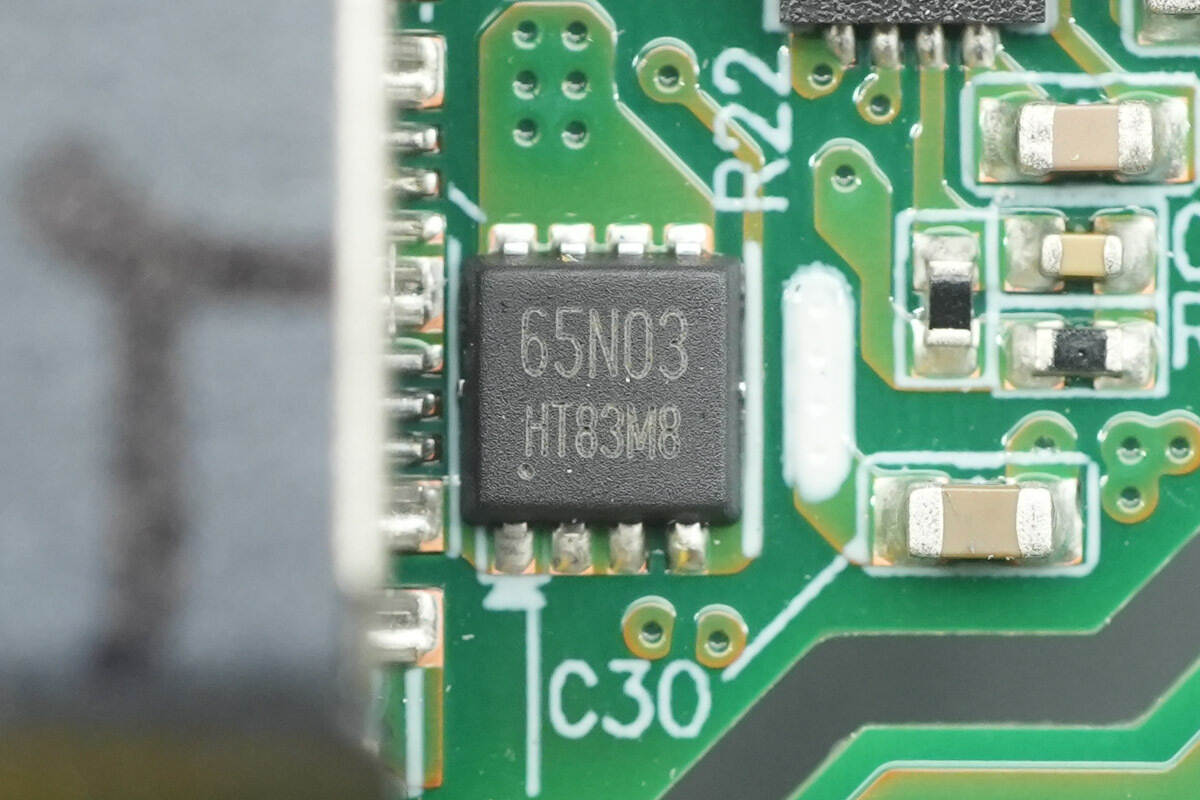
The output VBUS MOSFET is marked 65N03 and comes in a 3×3 mm DFN package.
Well, those are all components of the Samsung 60W Low Standby GaN Charger.
Summary of ChargerLAB
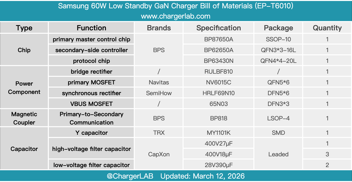
Here is the component list of the Samsung 60W Low Standby GaN Charger for your convenience.
It features fixed prongs and a single USB-C port, supporting PD 3.0, PPS, and QC5 fast-charging protocols, capable of delivering up to 60 W fast charging for flagship devices such as the Samsung Galaxy S26 Ultra. Under no-load conditions at 110 V and 220 V, its standby power consumption is 1.23 mW and 1.8 mW, respectively, well below the 5 mW zero-standby threshold specified by the IEC62301 standard, demonstrating outstanding energy efficiency.
After taking it apart, we found that it uses the BPS BP87650A + BP62650A zero-standby-power supply solution, paired with the patented magnetic-coupled communication feedback component BP818. This allows primary-to-secondary communication without a bias current, fundamentally eliminating standby losses from the feedback loop. The protocol chip is the BPS BP63430N, providing a complete solution from primary-side control to secondary-side protocol management.
It is this deeply integrated solution that enables Samsung’s fast-charging products to achieve milliwatt-level standby power, fulfilling its energy efficiency commitments. The inclusion of the full BPS zero-standby solution in Samsung’s global flagship smartphone charger supply chain also reflects Samsung’s strong recognition of the technological maturity, product stability, and mass-production capability of the BPS solution, marking a milestone in which domestic analog chips have demonstrated the ability to compete alongside top international manufacturers in the high-end fast-charging sector.
Related Articles:
1. Teardown of MORNSUN 550W Platinum SiC Server Power Supply (LMS550-P12B)
2. Teardown of Apple 40W Dynamic Power Adapter (A3365, HK Version)
3. Teardown of Apple M4 Mac mini (A3238)