Introduction
As a globally recognized consumer electronics giant, Samsung also possesses deep technical expertise in mobile accessories. Recently, Samsung launched a 5000 mAh magnetic wireless charging power bank supporting the Qi2 standard. The product features a compact and refined design, with a built-in foldable aluminum alloy stand, and supports 15 W Qi2 magnetic wireless charging as well as 25 W wired fast charging, meeting the everyday charging needs of modern smartphone users. Next, we will take a closer look at the design of this product.
Product Appearance
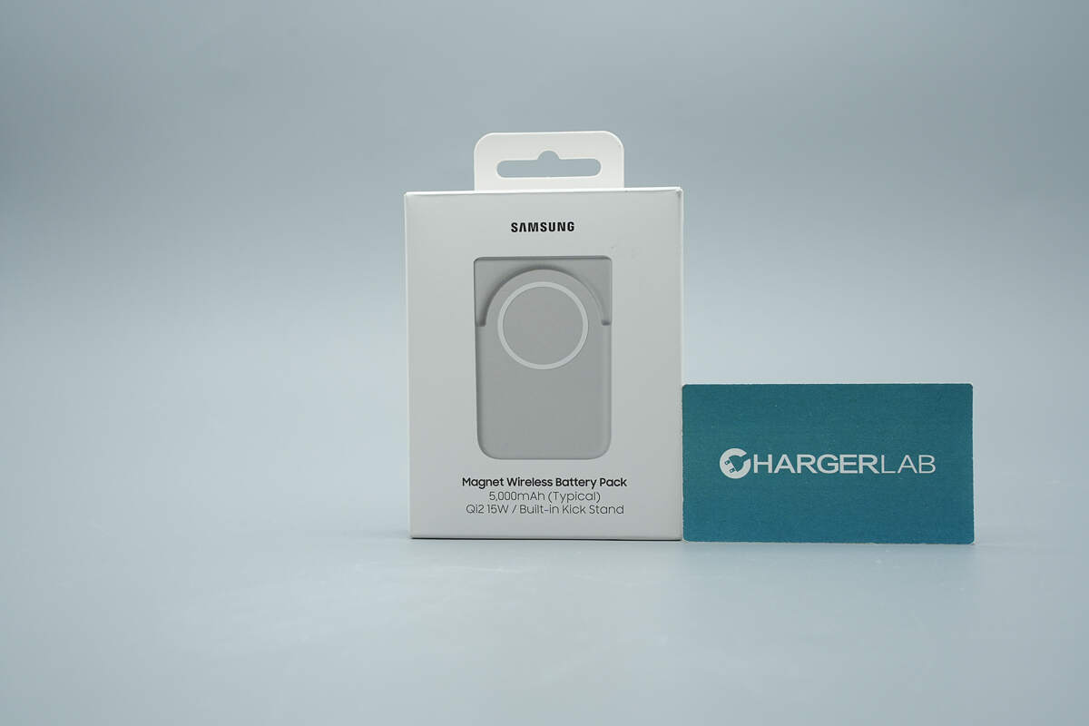
The top of the packaging features a hanging tab. A product rendering is displayed at the center, with the product name and “Qi2 15W” printed below.
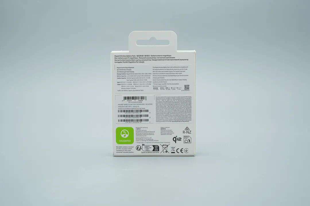
The back displays the technical specifications, manufacturing information, a barcode, and various safety and environmental certification marks.
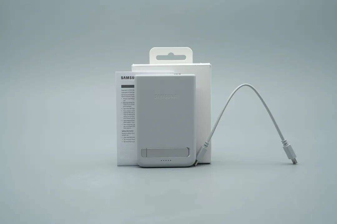
The package includes a power bank, a short dual USB-C cable, and a user manual.
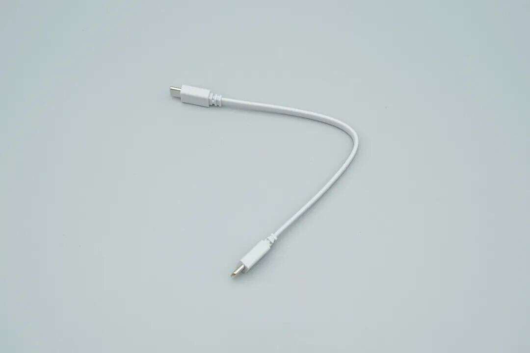
The short dual USB-C cable is well-suited for use with the power bank on the go.
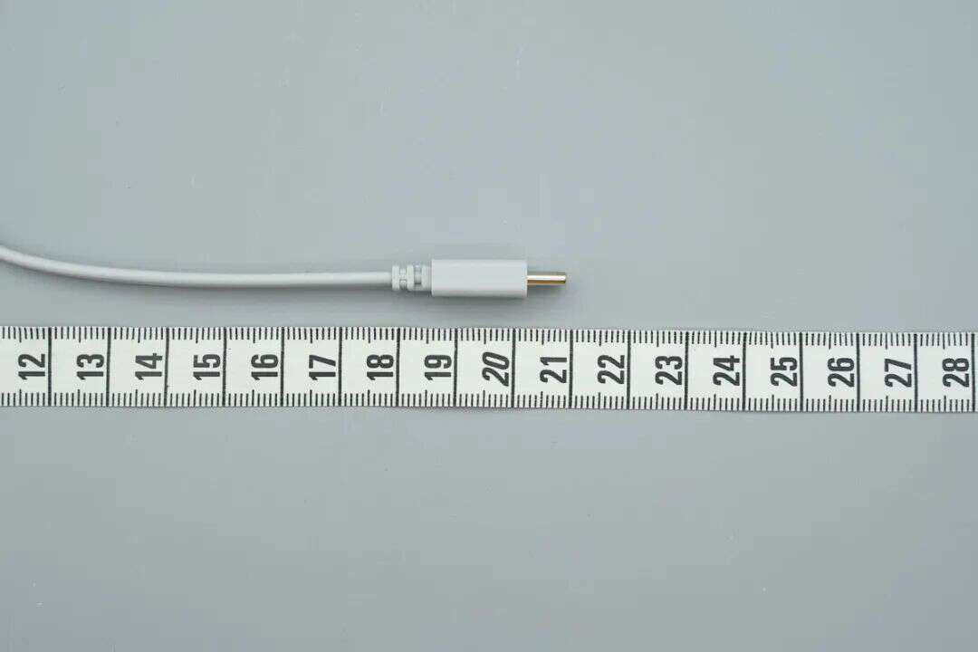
The length of the cable is about 20 cm (7.87 inches).
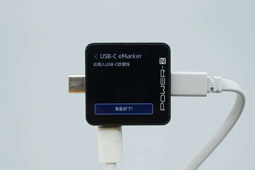
ChargerLAB POWER-Z KM003C indicates that it does not feature an E-Marker chip.
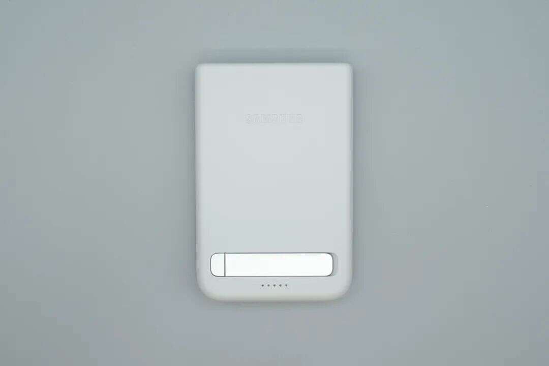
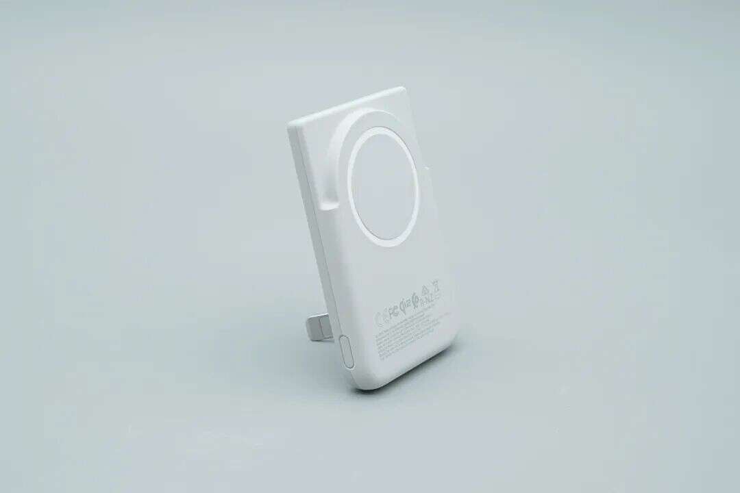
The enclosure features a grayish-white, skin-friendly finish, with the Samsung logo centered. The bottom is equipped with an aluminum alloy folding stand and indicator lights.
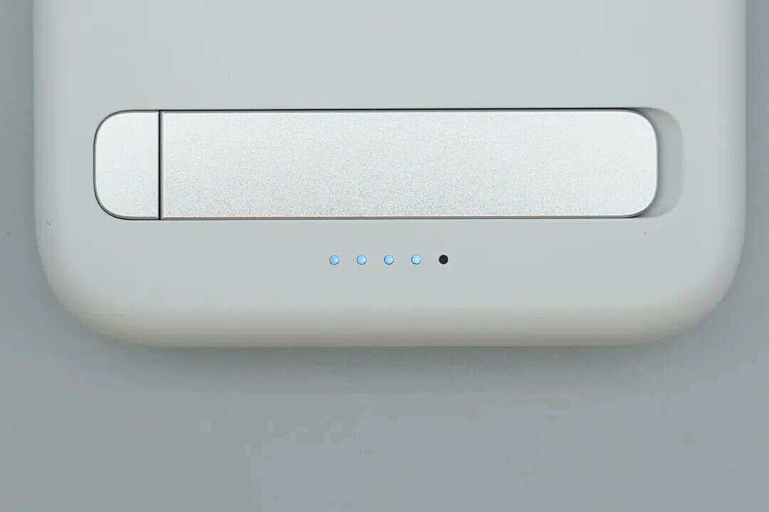
The aluminum alloy stand on the bottom is finely crafted and features a sandblasted metal finish. The bottom also includes white LED battery level indicators, with the rightmost light indicating fast charging status.
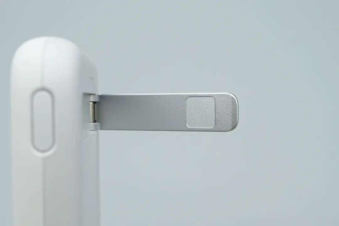
When the metal stand is unfolded, the hinge provides a well-damped, smooth resistance.
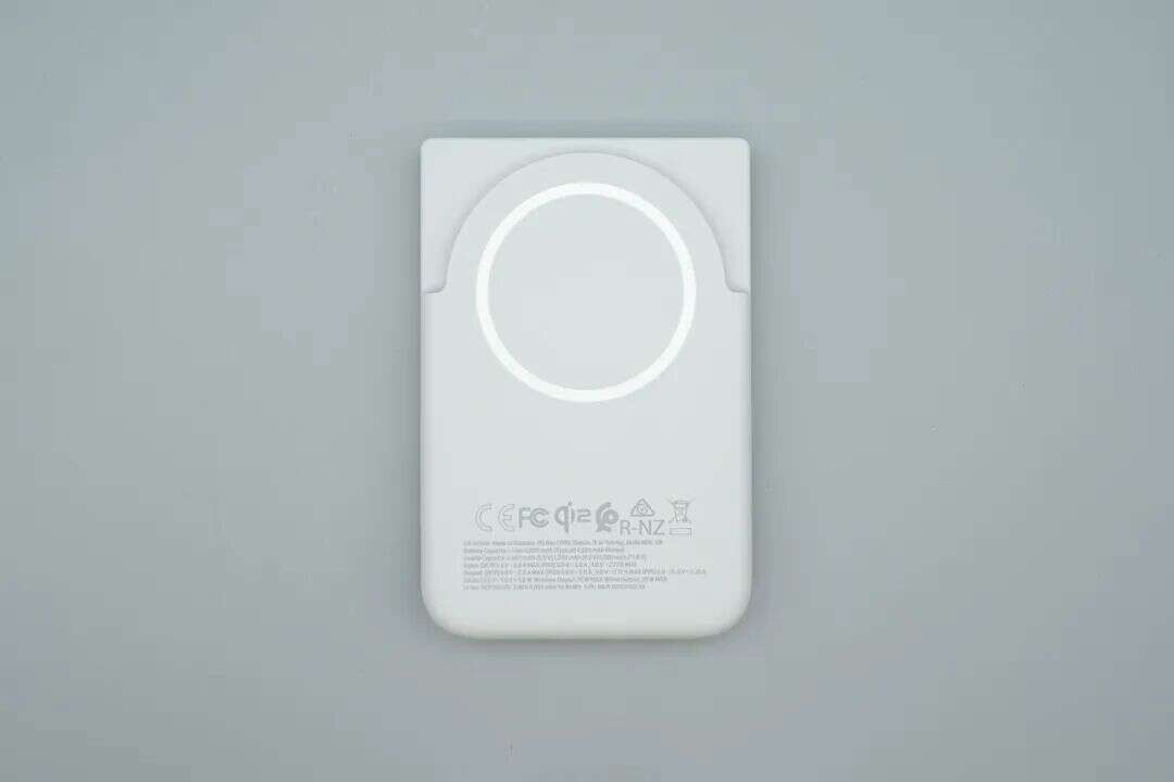
The back of the power bank features a circular magnetic alignment area. The top sides have recesses that do not obstruct the camera, and the bottom displays relevant certifications and specifications.
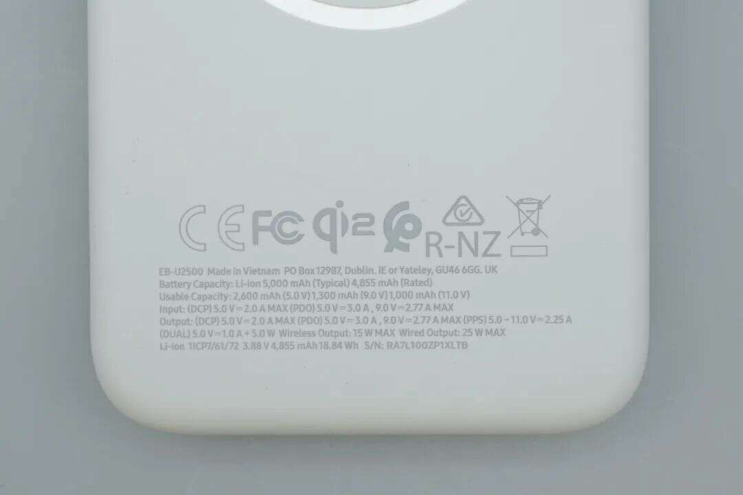
Model: EB-U2500
Battery capacity:
5,000 mAh (typical), 4,855 mAh (rated)
Usable capacity:
2,600 mAh (5.0 V)
1,300 mAh (9.0 V)
1,000 mAh (11.0 V)
Input:
(DCP) 5.0 V ⎓ 2.0 A MAX
(PDO) 5.0 V ⎓ 3.0 A, 9.0 V ⎓ 2.77 A MAX
Output:
(DCP) 5.0 V ⎓ 2.0 A MAX
(PDO) 5.0 V ⎓ 3.0 A, 9.0 V ⎓ 2.77 A MAX
(PPS) 5.0–11.0 V ⎓ 2.25 A
Dual output:
5.0 V ⎓ 1.0 A + 5.0 W
Wireless charging output: 15 W MAX
Maximum output: 25 W MAX
This product is made in Vietnam and has obtained CE, FCC, and various other certifications.
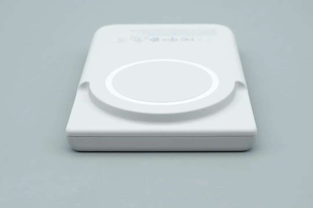
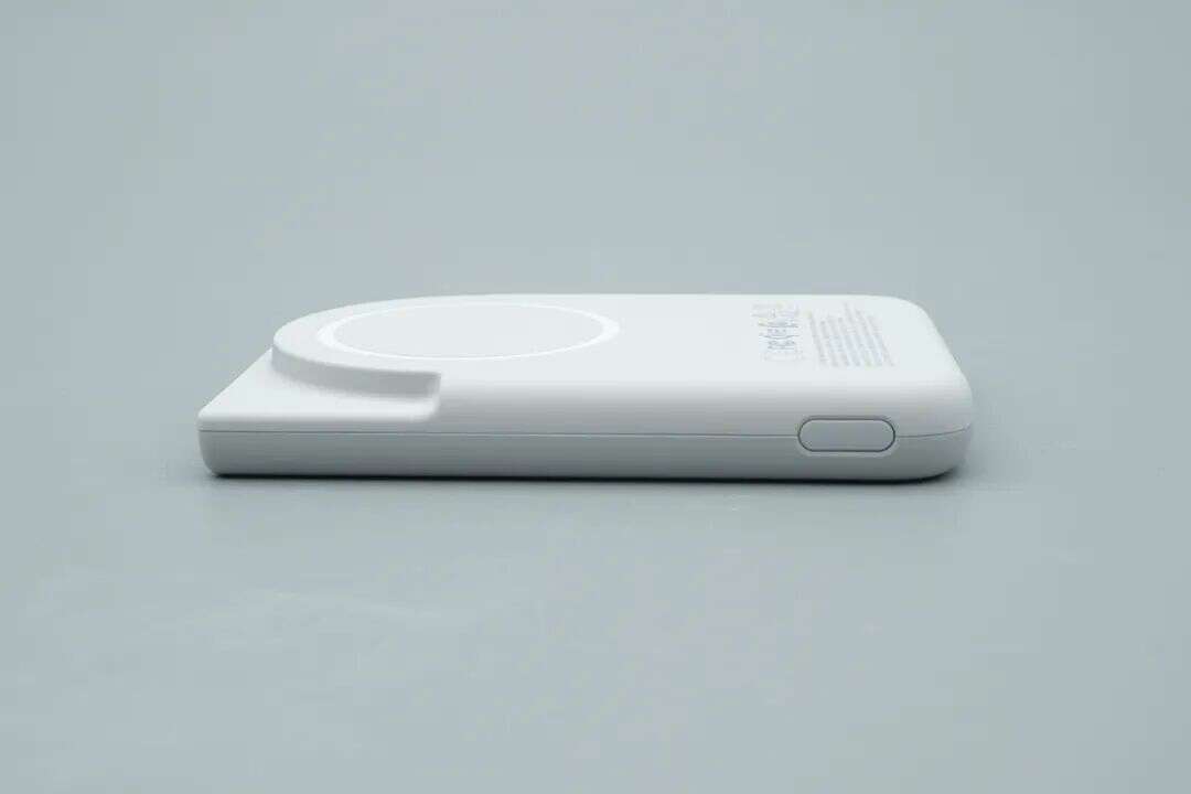
The wireless charging area features a stepped raised design, specifically tailored to accommodate the large rear camera modules of modern smartphones.
The edges of the power bank are smoothly rounded, with a recessed micro-switch power button located on the right side.
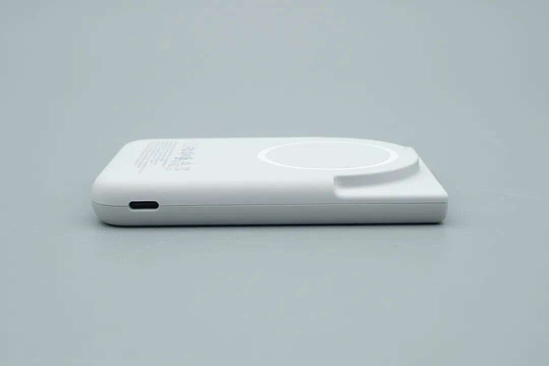
The opposite side features a USB-C port supporting bidirectional fast charging.
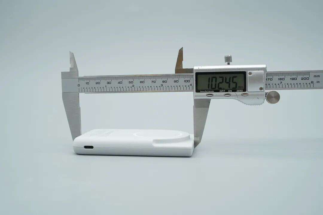
The length of the power bank is about 102.45 mm (4.033 inches).
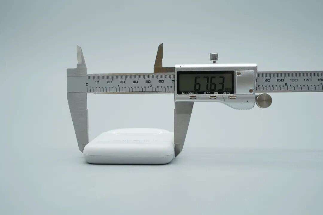
The width is about 67.63 mm (2.66 inches).
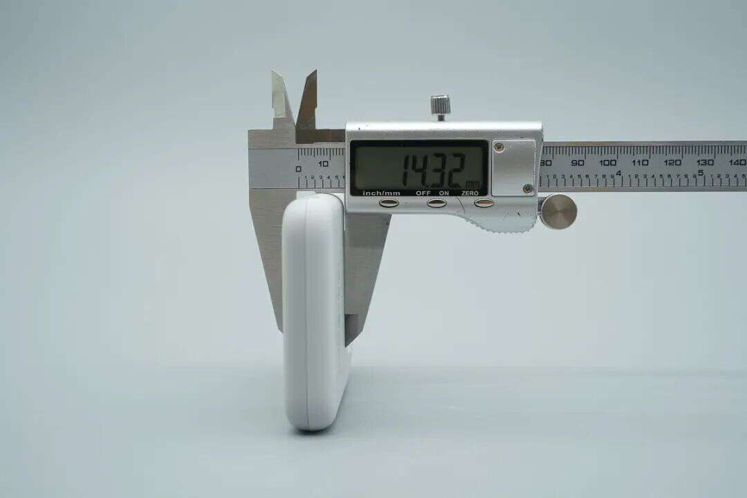
The thickness is about 14.32 mm (0.56 inches).
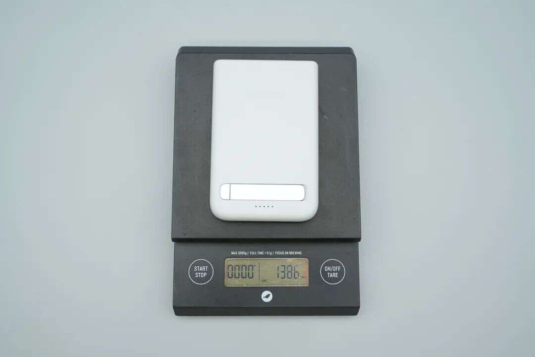
The weight is about 138.6 g (4.89 oz).
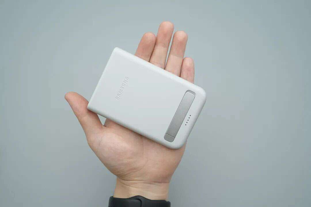
That's how big it is in the hand.
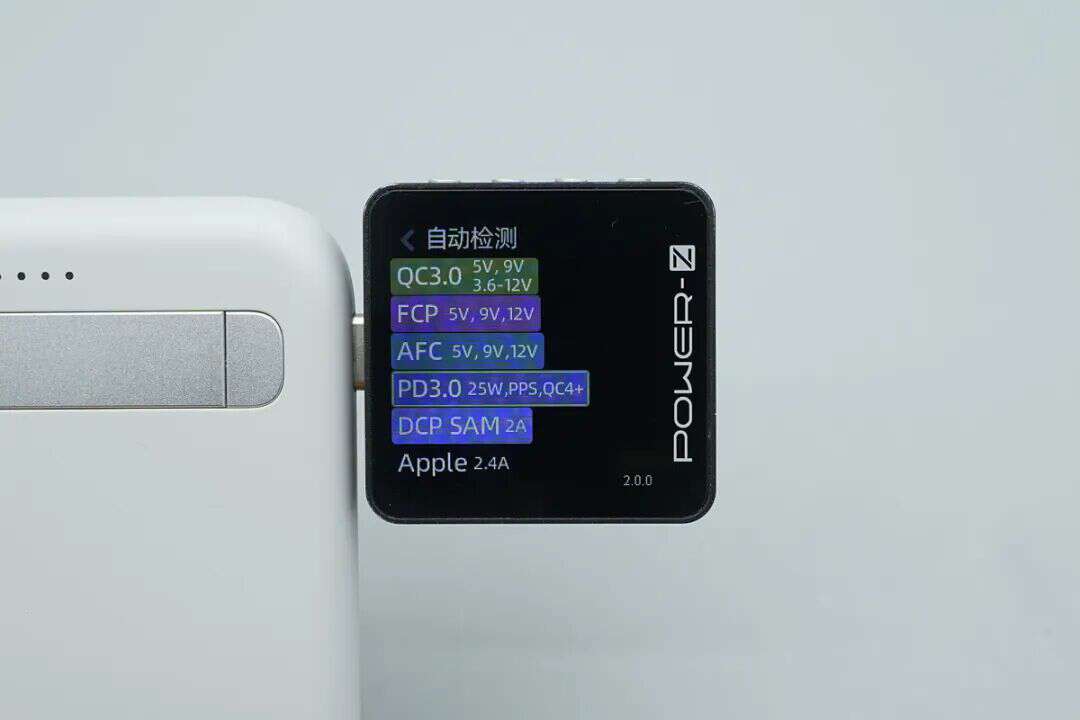
ChargerLAB POWER-Z KM003C shows that the USB-C port supports QC3.0, FCP, AFC, PD3.0, PPS, DCP, SAMSUNG 2A, and Apple 2.4A charging protocols.
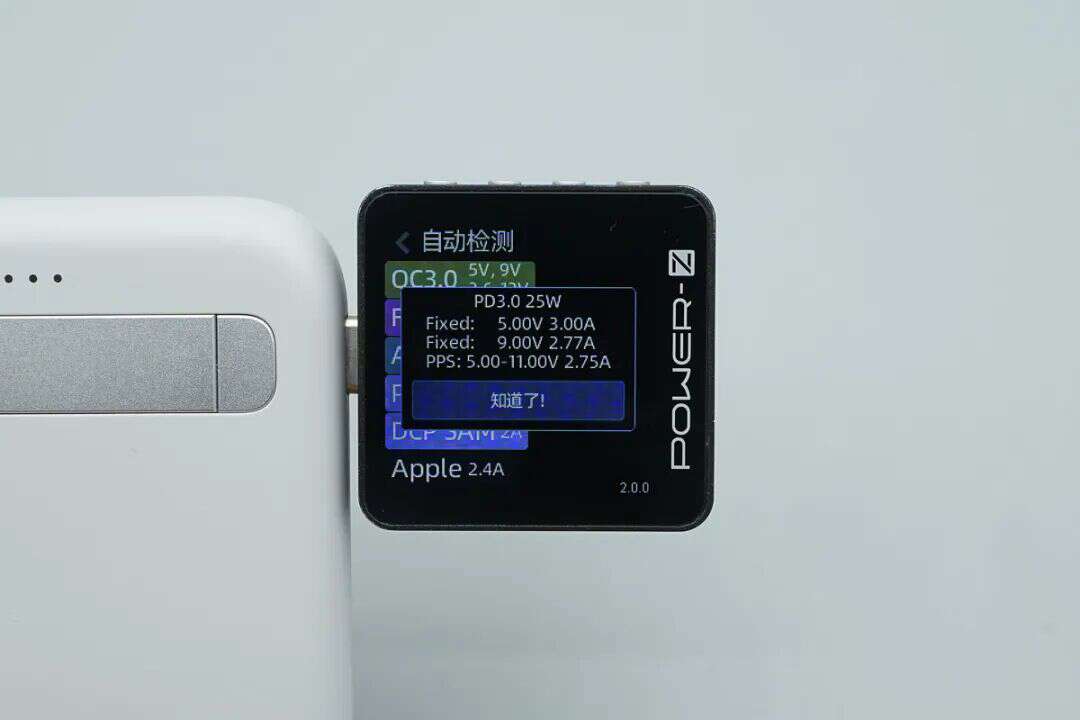
It also supports two fixed PDOs of 5 V⎓3 A and 9 V⎓2.77 A, as well as a PPS voltage range of 5.00–11.00 V⎓2.25 A.
When the metal stand is unfolded, the power bank can be placed securely on a flat surface.
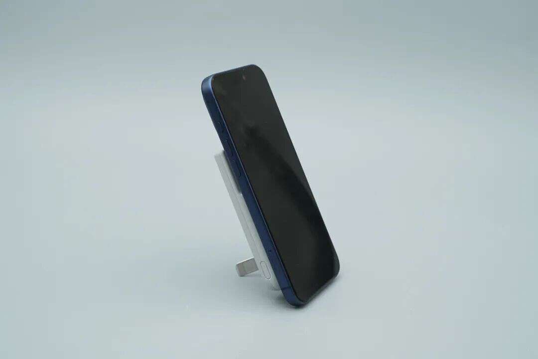
A usage scenario with an iPhone is shown in the illustration.
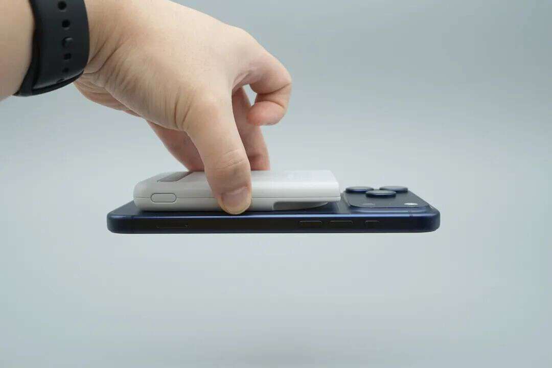
The magnetic attachment is strong enough to hold the phone securely, even when inverted.
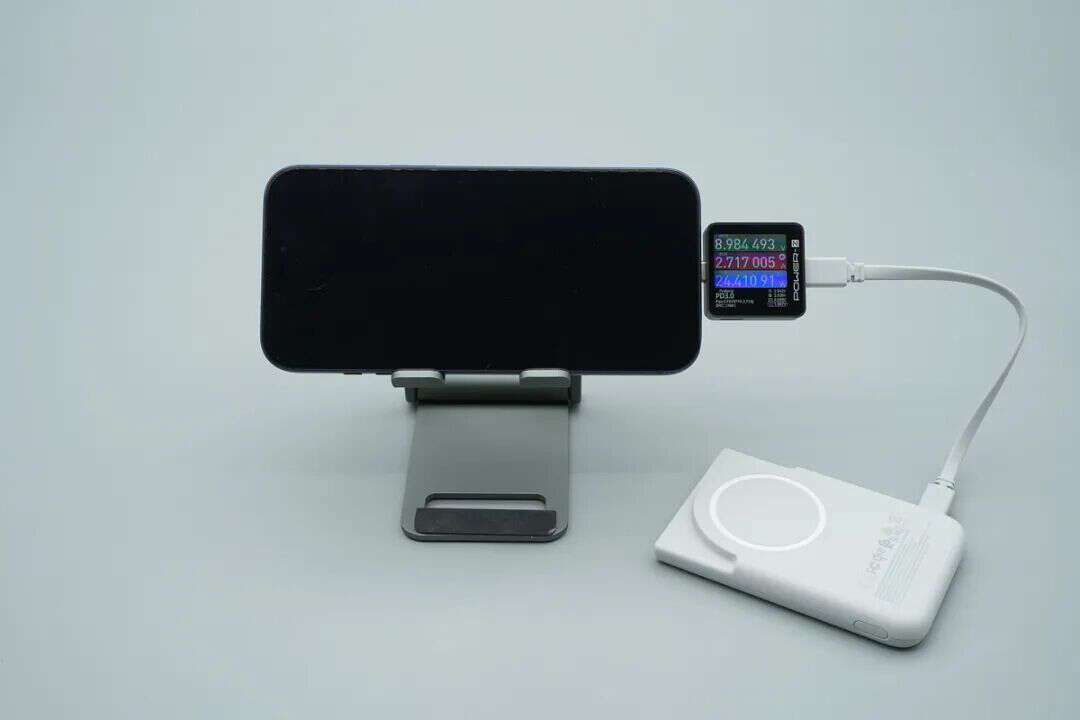
ChargerLAB POWER-Z KM003C shows that the wired output can reach 8.98 V ⎓ 2.71 A (24.41 W), successfully enabling PD fast charging.
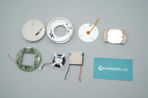
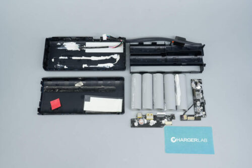
Teardown
Next, let's take it apart to see its internal components and structure.
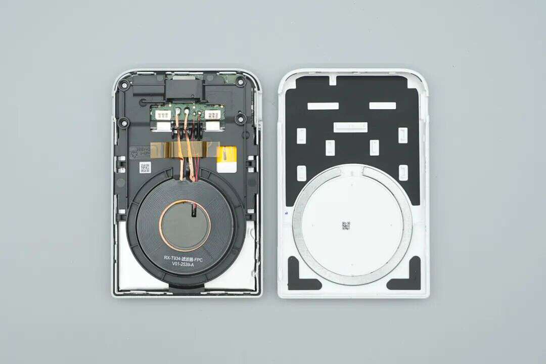
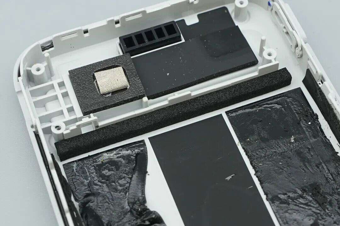
Prying open the front panel along the seams reveals that the PCBA module is largely covered by plastic sheets. A metal magnetic induction plate is attached to the center of the front cover, while black foam and graphite thermal pads are distributed around the edges for cushioning, isolation, and enhanced heat dissipation.
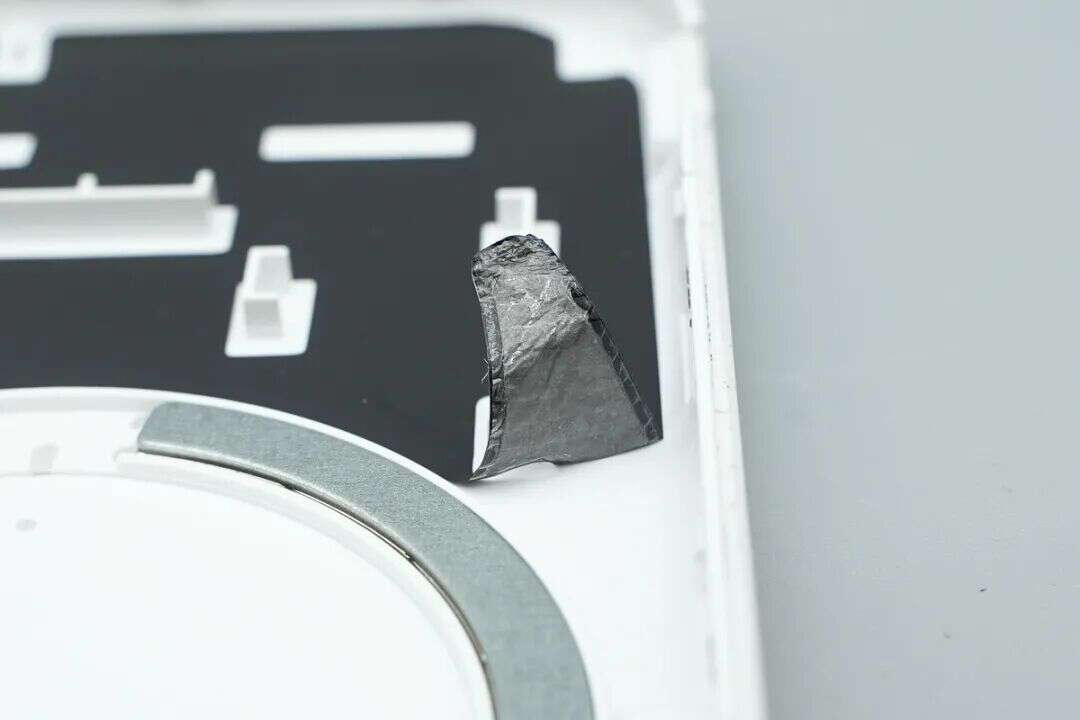
Peeling back a corner of the black protective tape on the front cover confirms that it is a graphite thermal pad.
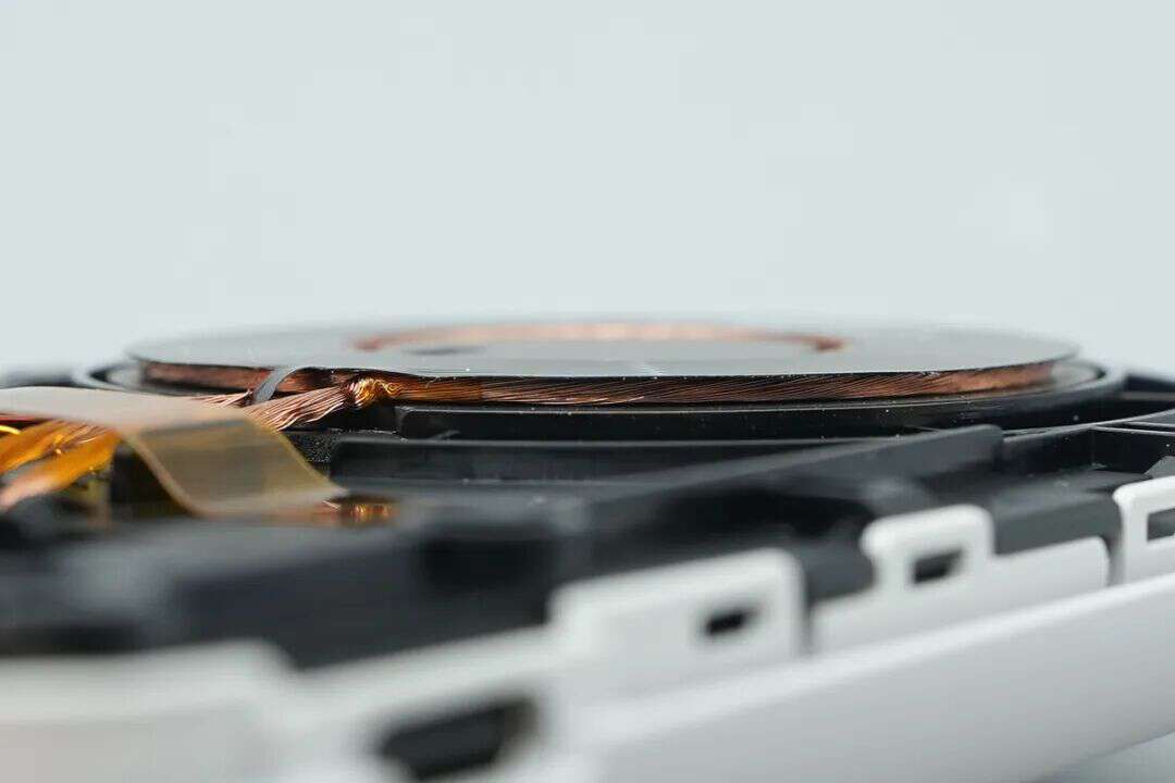
The wireless charging coil is tightly wound using multi-stranded Litz wire, with the outer layer insulated by a black adhesive tape.
A thermistor is located at the center of the coil.
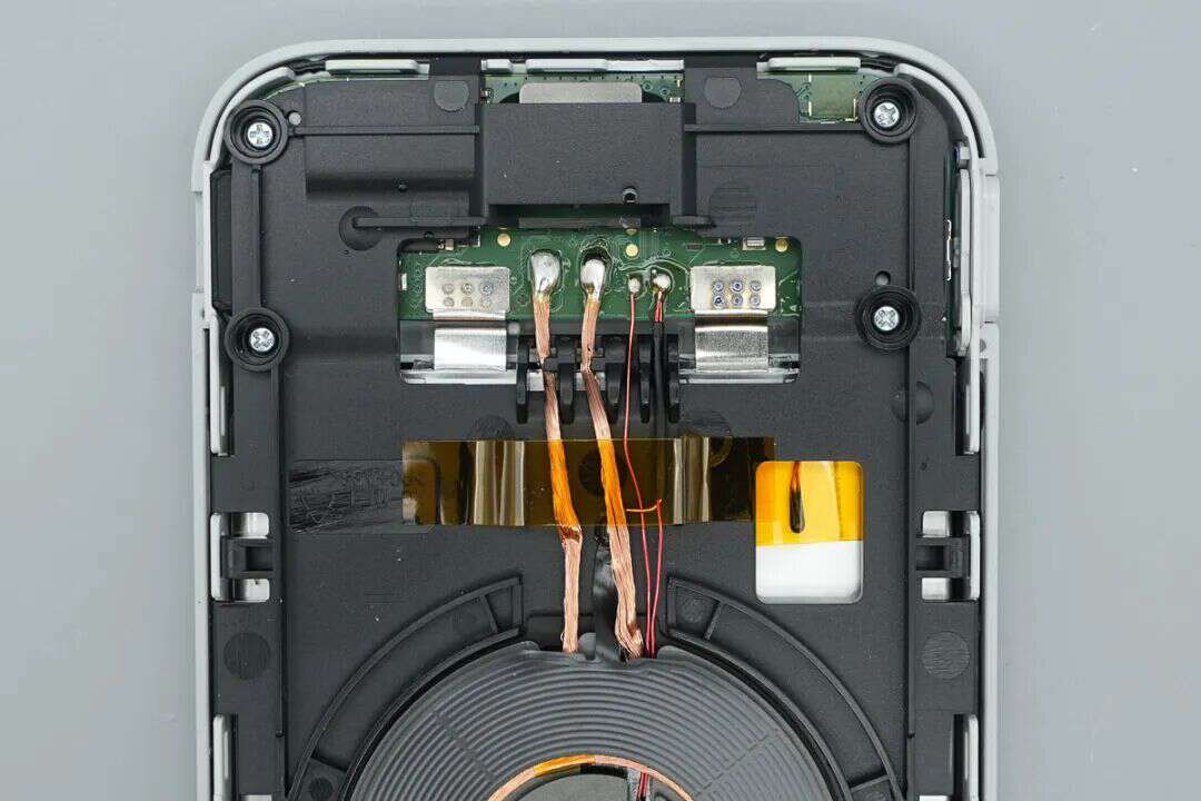
In the PCBA area, only the connection wires to the coil and a few metal pads for the thermistor are exposed.
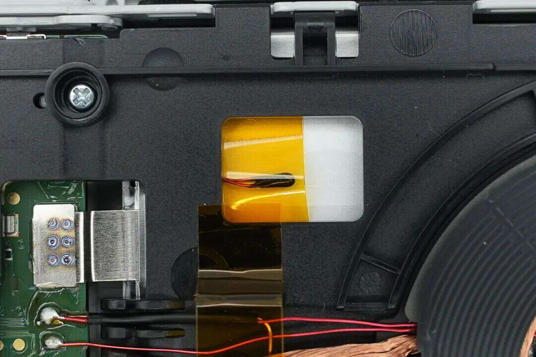
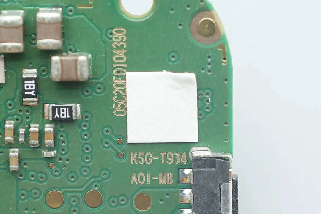
A yellow high-temperature insulating tape is applied to the cutout area on the right side of the plastic cover, covering a thermistor used to monitor the battery pack temperature.
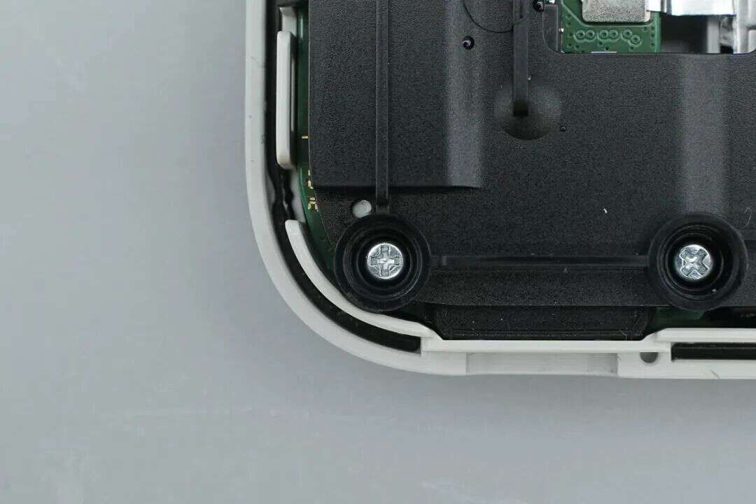
The black plastic cover is secured with four screws.
The coil, wiring, and plastic cover are stacked tightly, with the overall thickness minimized to near the design limit.
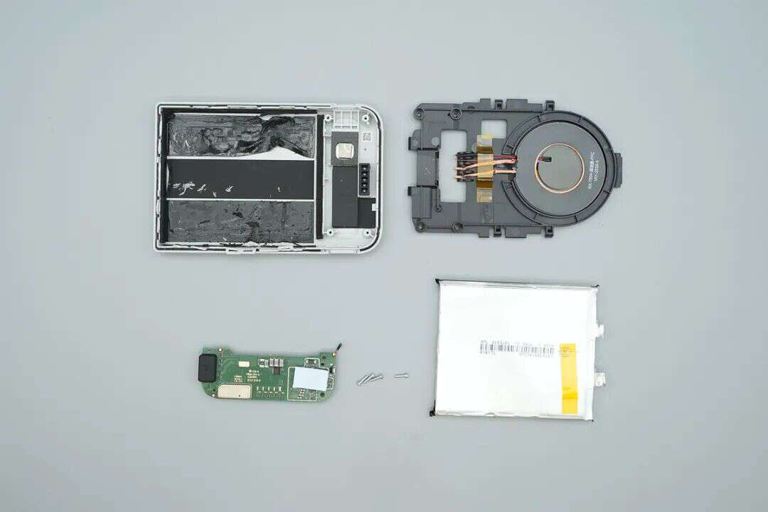
Unscrew all the screws to separate the core module.
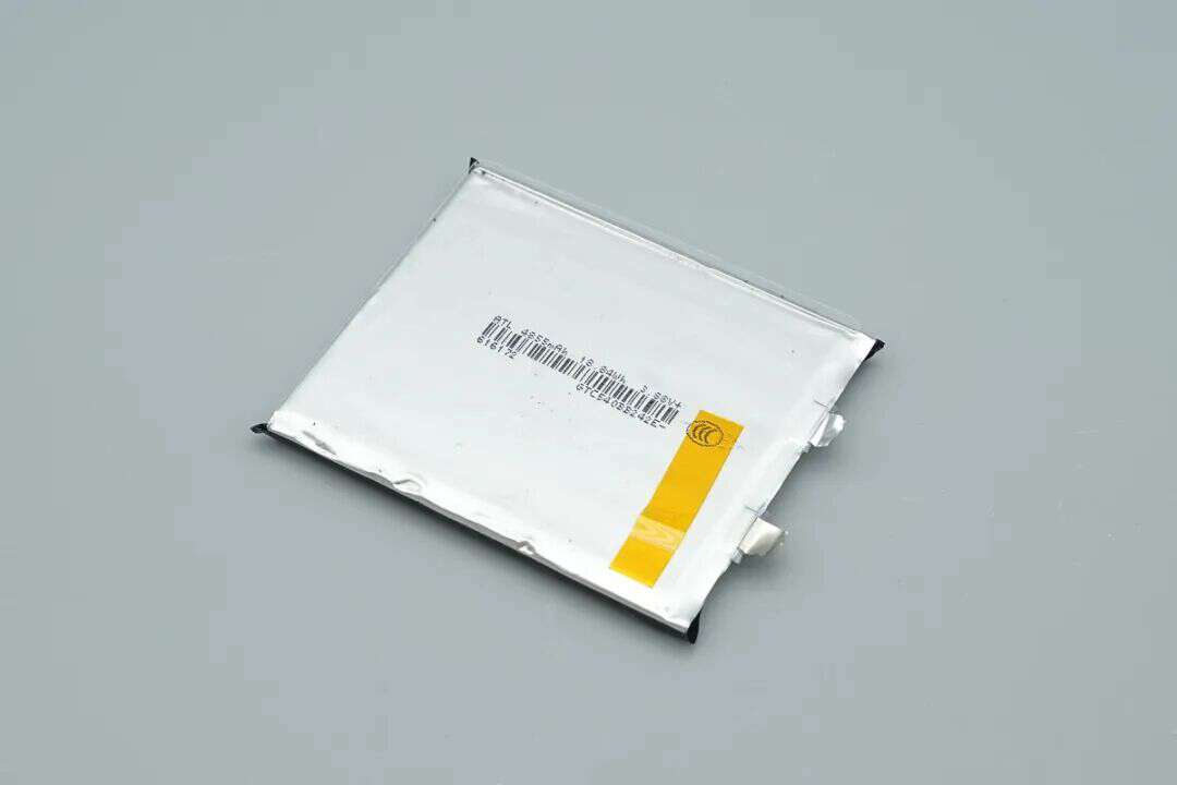
The pouch-type lithium-ion cell is wrapped in a silver-colored film.
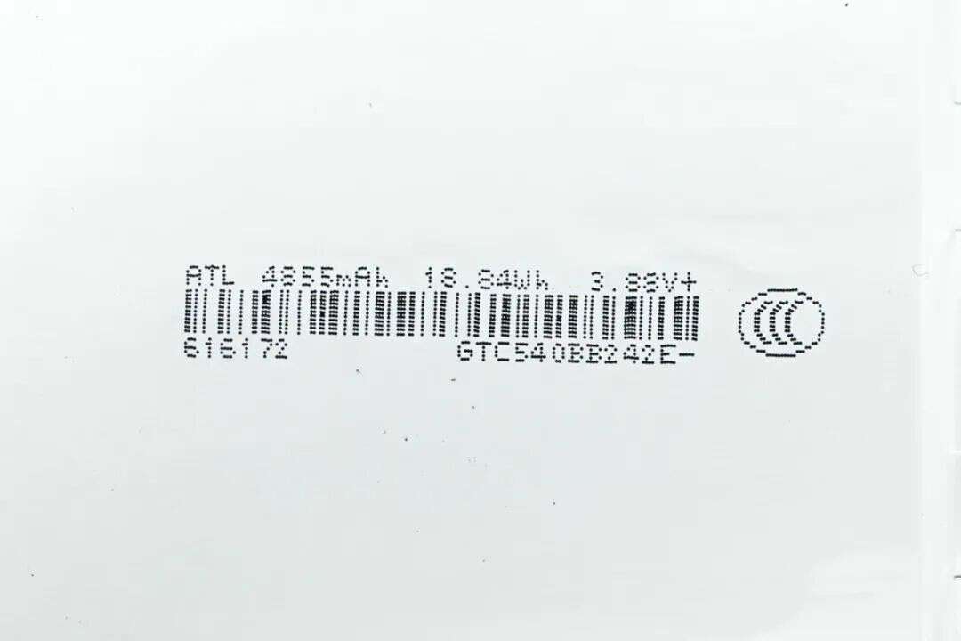
The cell is sourced from ATL, with a capacity of 4855 mAh, energy of 18.84 Wh, and voltage of 3.88 V, and it is CCC certified.
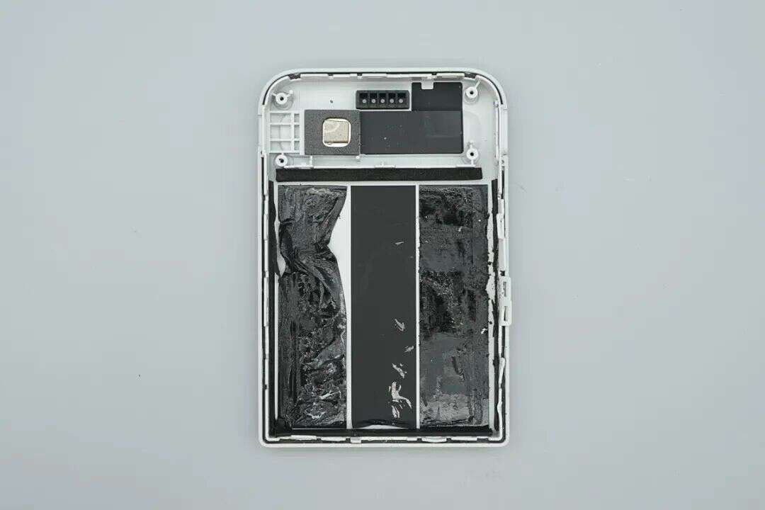
A large area inside the bottom casing is covered with black, strong adhesive to firmly secure the battery.
A metal braided conductive fabric and a black anti-vibration foam strip are applied at the PCBA module location to contact the grounding area, providing electromagnetic shielding.
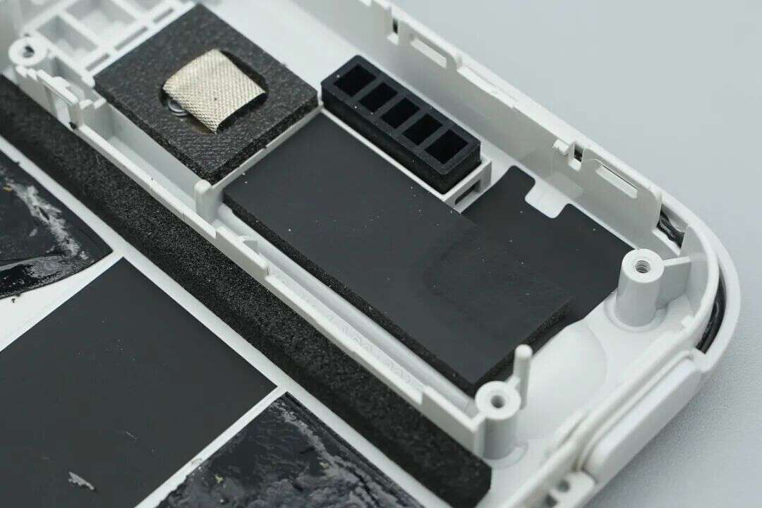
Each LED indicator slot is individually separated to prevent light leakage between the lamps.
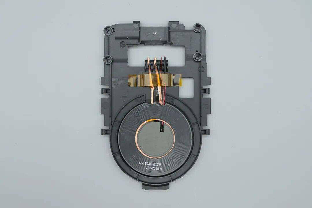
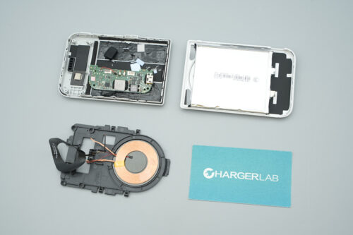
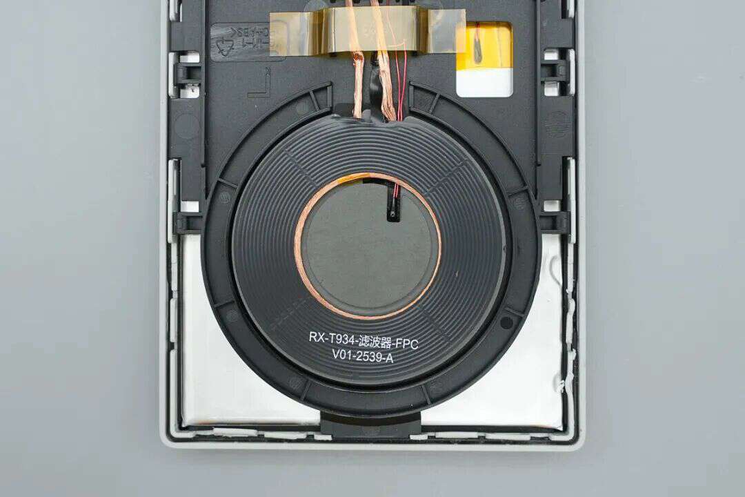
Front view of the black middle frame with the magnetic wireless charging coil, featuring a large opening at the top for wire routing.
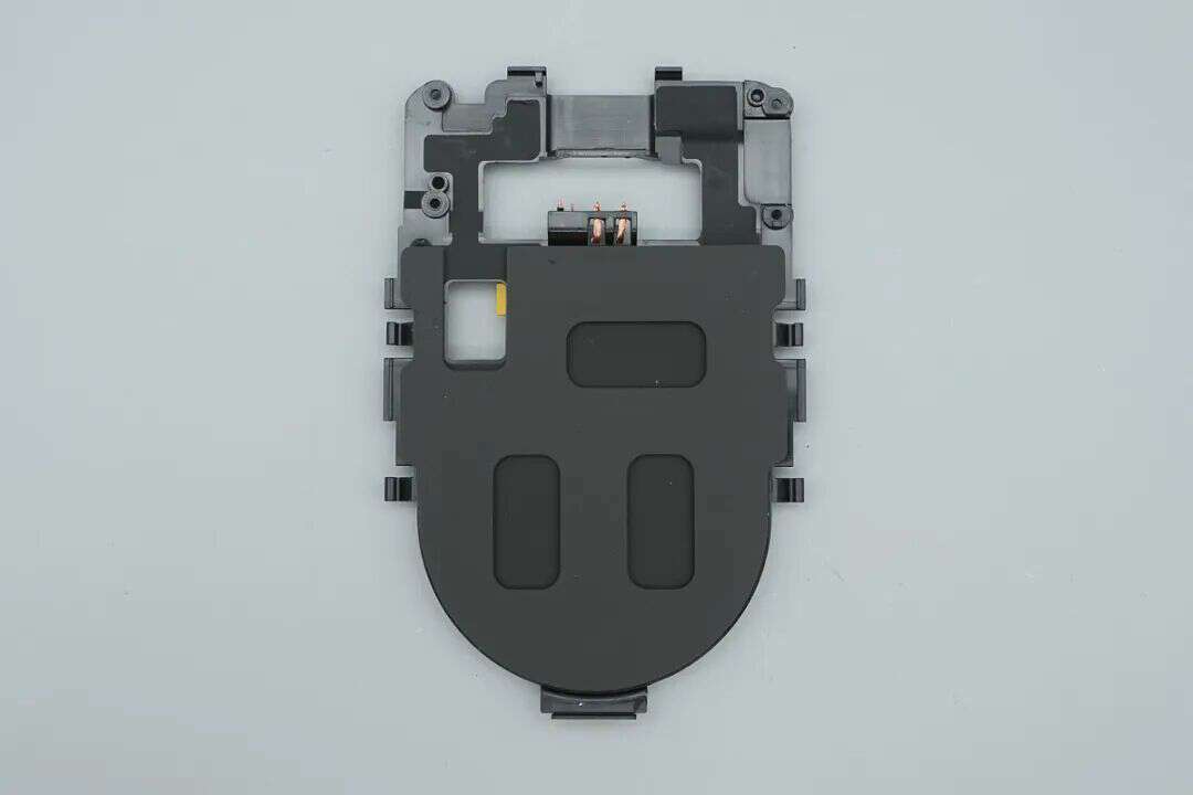
The back of the middle frame has a flat surface with a large black insulating pad applied to the battery contact area.
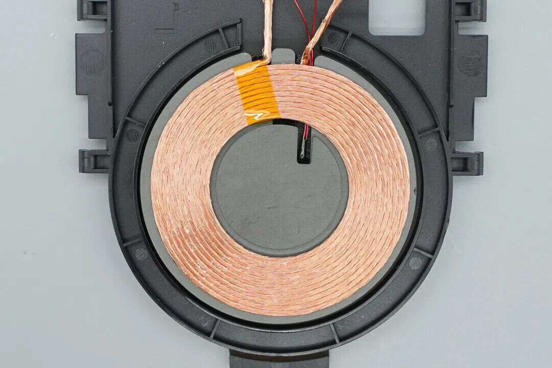
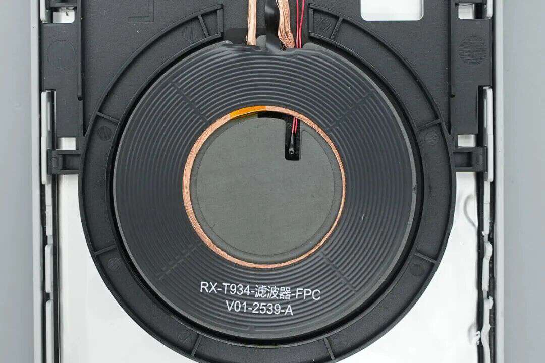
Peel off the insulation protective film on the front of the coil to reveal the wireless charging transmitter coil, with the Litz wire arranged neatly and tightly, demonstrating solid workmanship.
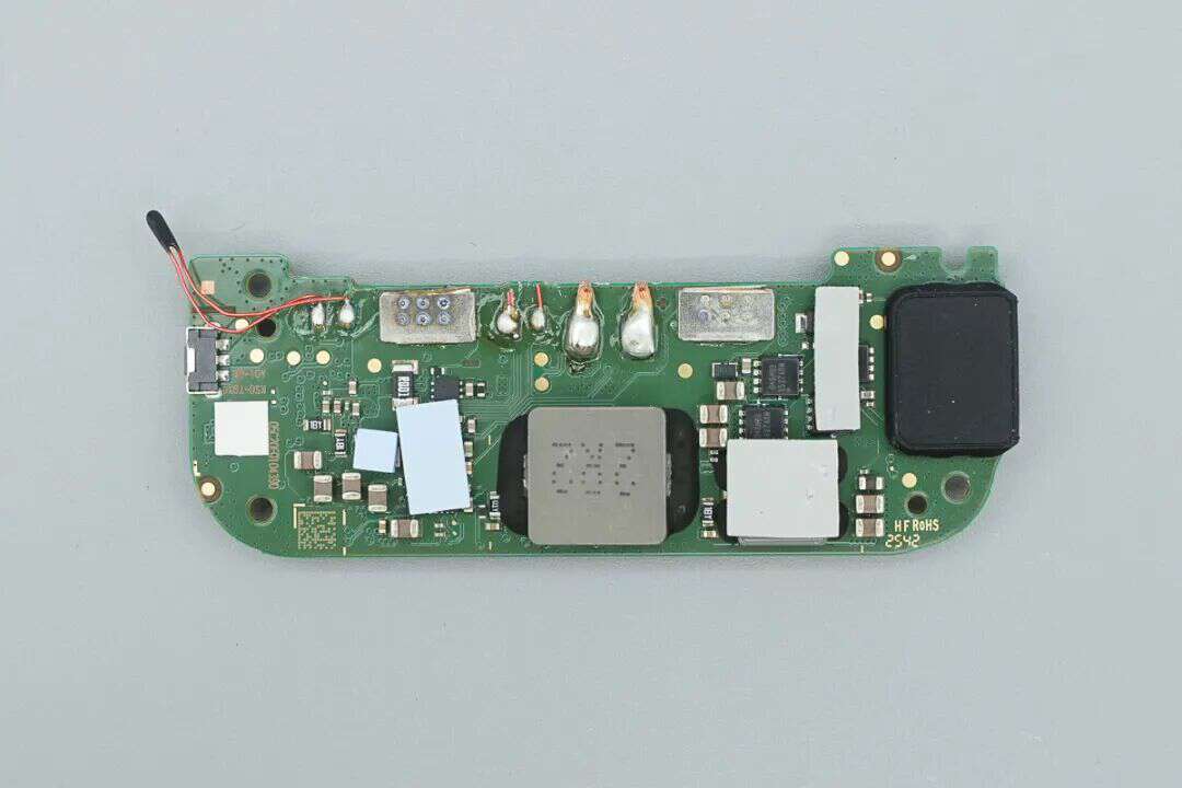
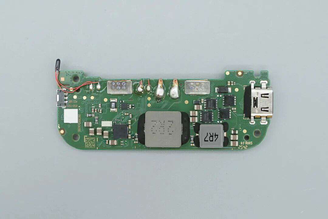
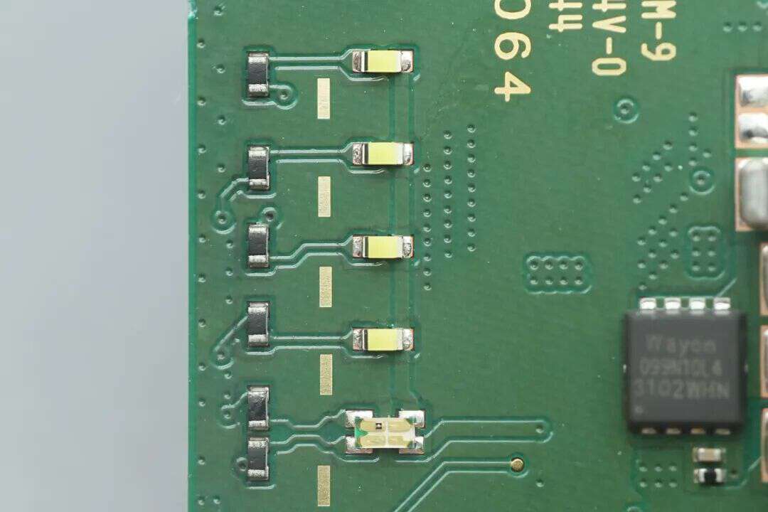
The front of the PCBA module features a USB-C female connector, two buck-boost alloy inductors, several filter capacitors, and a micro push-button switch.
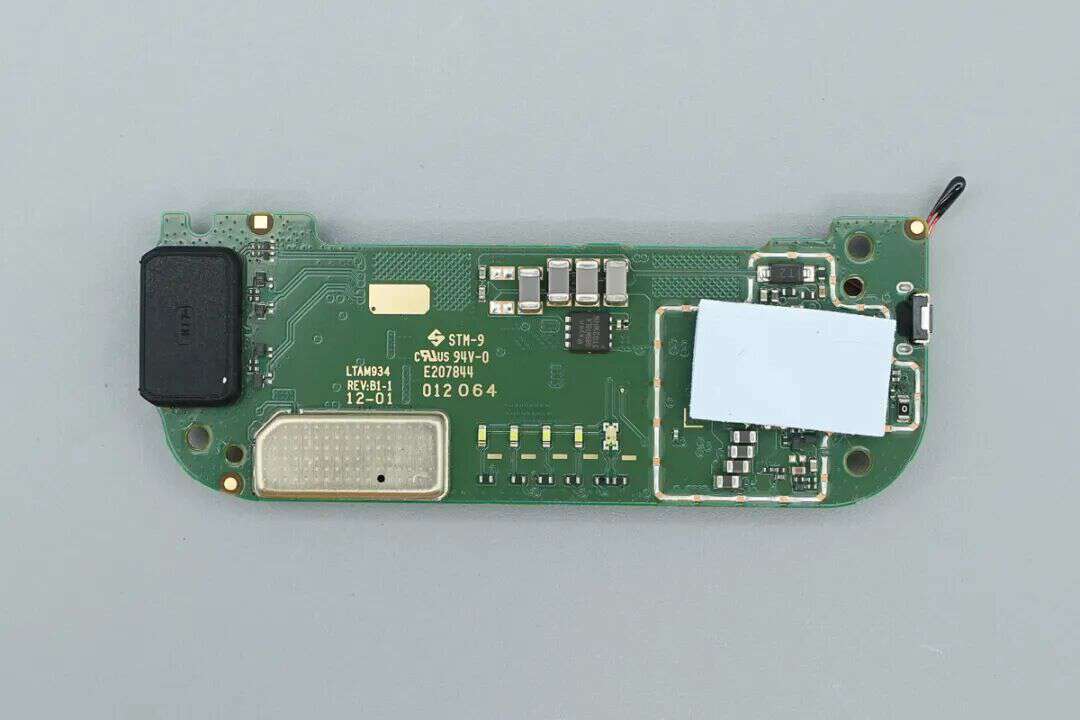
The back is marked with “STM-9” and the UL94V-0 flammability rating. A thick thermal pad covers the control chip area on the right side.
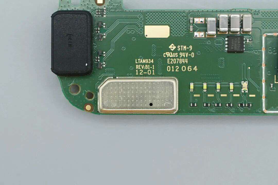
Close-up of the back showing the shielding cover and the five LED indicators for battery level and status.
Remove the thermal silicone pads from both the front and back sides.
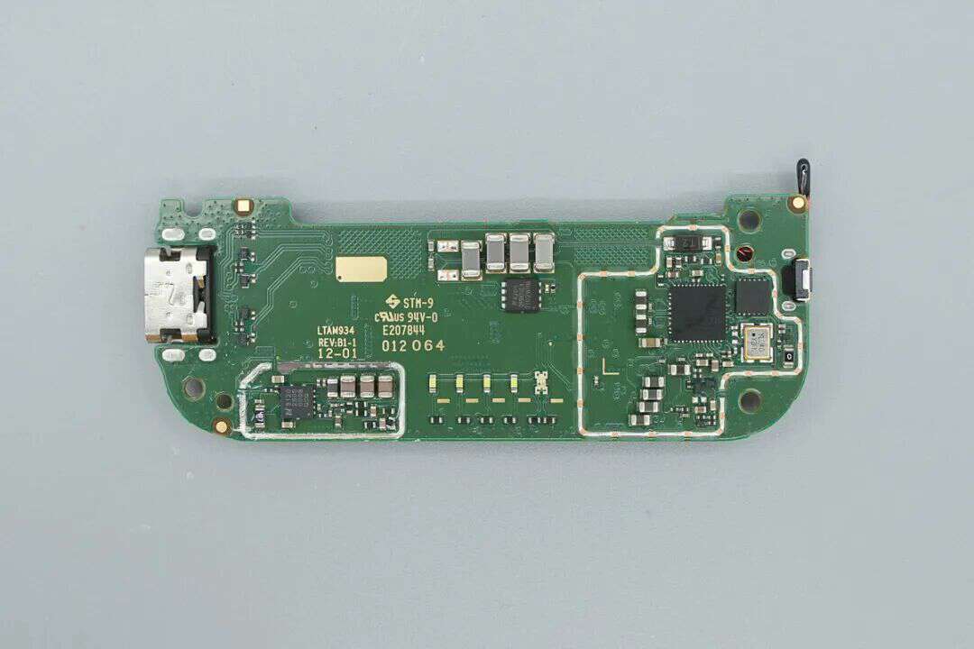
Rear view after removing the thermal pad and shielding cover.
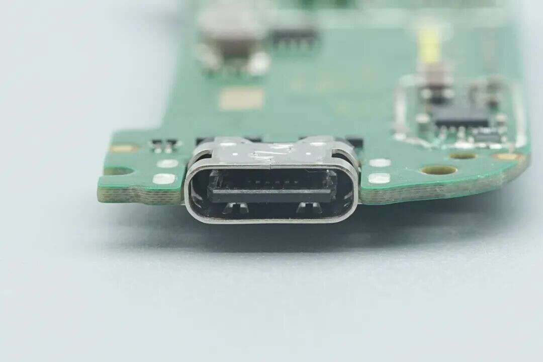
The USB-C socket is soldered via recessed plated through-holes, with a black plastic sheet.
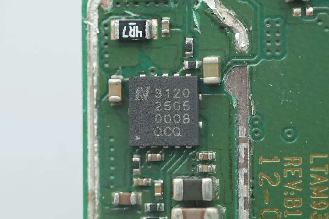
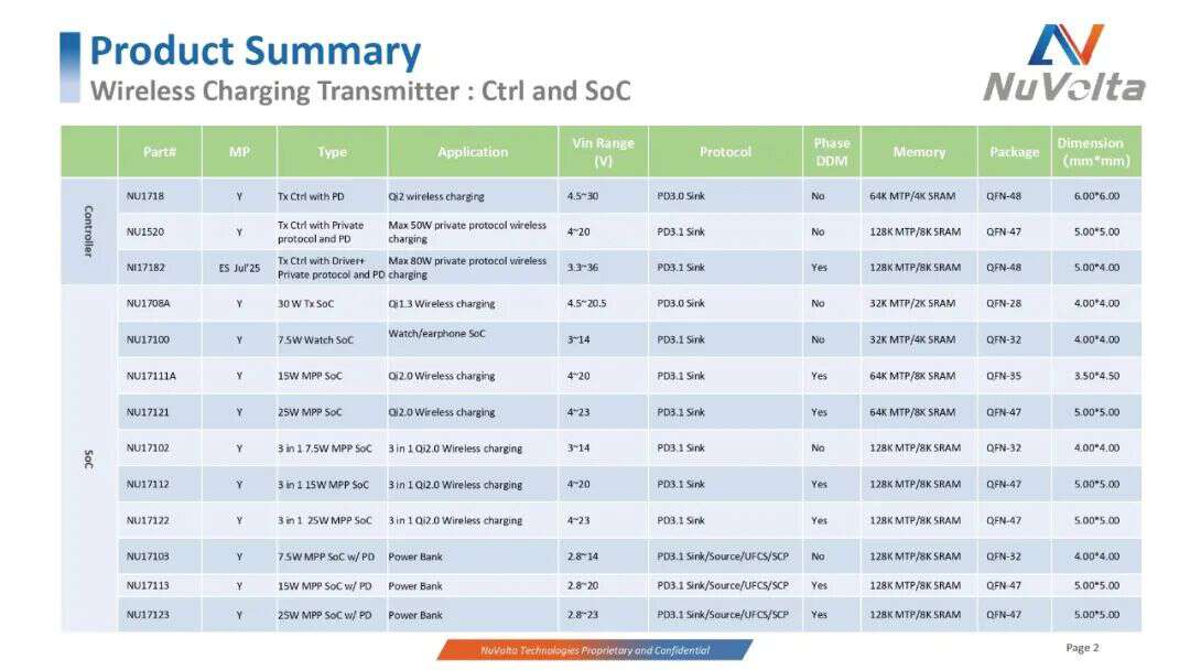
Inside the shielding cover, the synchronous boost converter is from NuVolta, model NU3120. This highly integrated design meets the compact internal space requirements of this Samsung power bank and, together with two additional NuVolta ICs, enables simultaneous charging and discharging, supporting 15 W MPP operation.
The chip comes in a QFN13 package, integrating a 10 mΩ MOSFET and a 16 mΩ rectifier, significantly simplifying the peripheral circuit design and providing a compact solution for portable devices. It supports a wide input voltage range of 2.9 V to 18 V, offers 10 A continuous switching current capability, and can deliver a maximum output voltage of 20 V. It also supports PFM and PWM mode switching, balancing high efficiency with stable operation.
Close-up of the five LED indicators, with the bottom one being a bi-color LED.
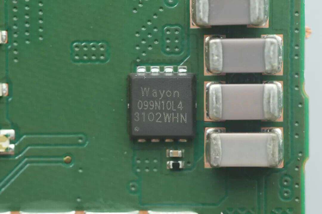
The wireless charging resonant capacitor switching MOSFET is marked “099N10L4,” with the full model WMB099N10LG4, from Wayon. It comes in a PDFN5060 package, is an NMOS type, rated for 100 V, with an on-resistance of 8 mΩ.
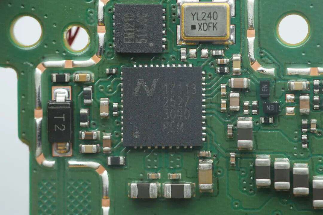
The master control SoC for the wireless charging power bank is from NuVolta, specifically designed for Qi2 wireless charging power banks. It supports 15 W MPP simultaneous charging and discharging, allowing the power bank to function as a desktop wireless charger when continuously connected to power.
The NU17113 comes in a QFN47 package, featuring a 32-bit MCU core, low-resistance full-bridge MOSFETs with integrated drivers, and built-in fast-charging protocols including PD, QC3.0, and UFCS. This integration simplifies the peripheral circuit design, reducing space requirements inside the compact power bank.
Additionally, the chip offers high-precision Q-factor detection, adjustable MOSFET power driving, and hardware frequency dithering to effectively reduce EMI. It also incorporates multiple safety protections, including overvoltage, overcurrent, and thermal shutdown, ensuring comprehensive stability for this Samsung product.
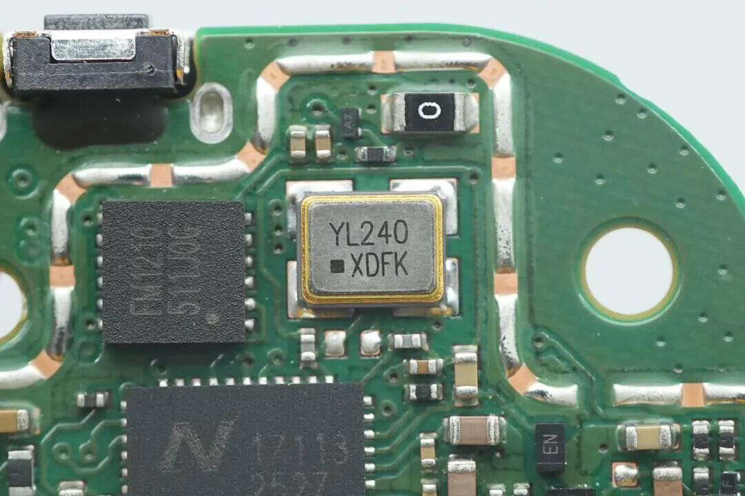
A crystal oscillator next to the wireless charging master control chip is marked “YL240.”
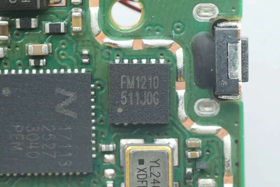
A FUDAN authentication chip marked “FM1210,” featuring data protection and address/data encryption, is used to meet the security encryption requirements of the Qi2 wireless charging standard. It comes in a DFN12 package.
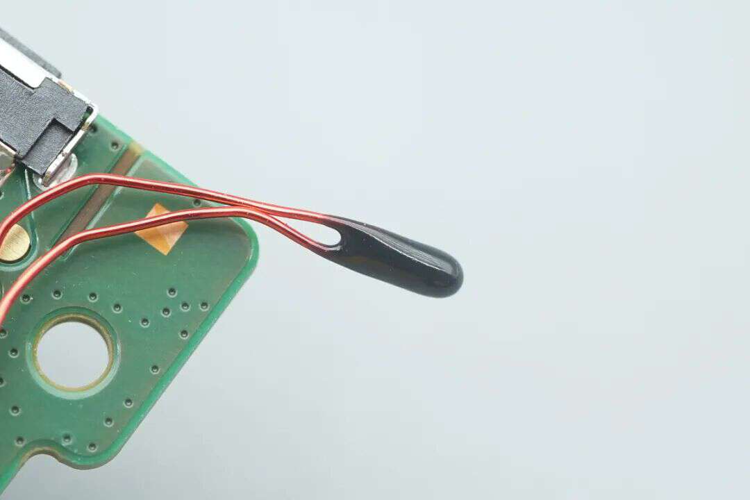
Close-up of the thermistor.
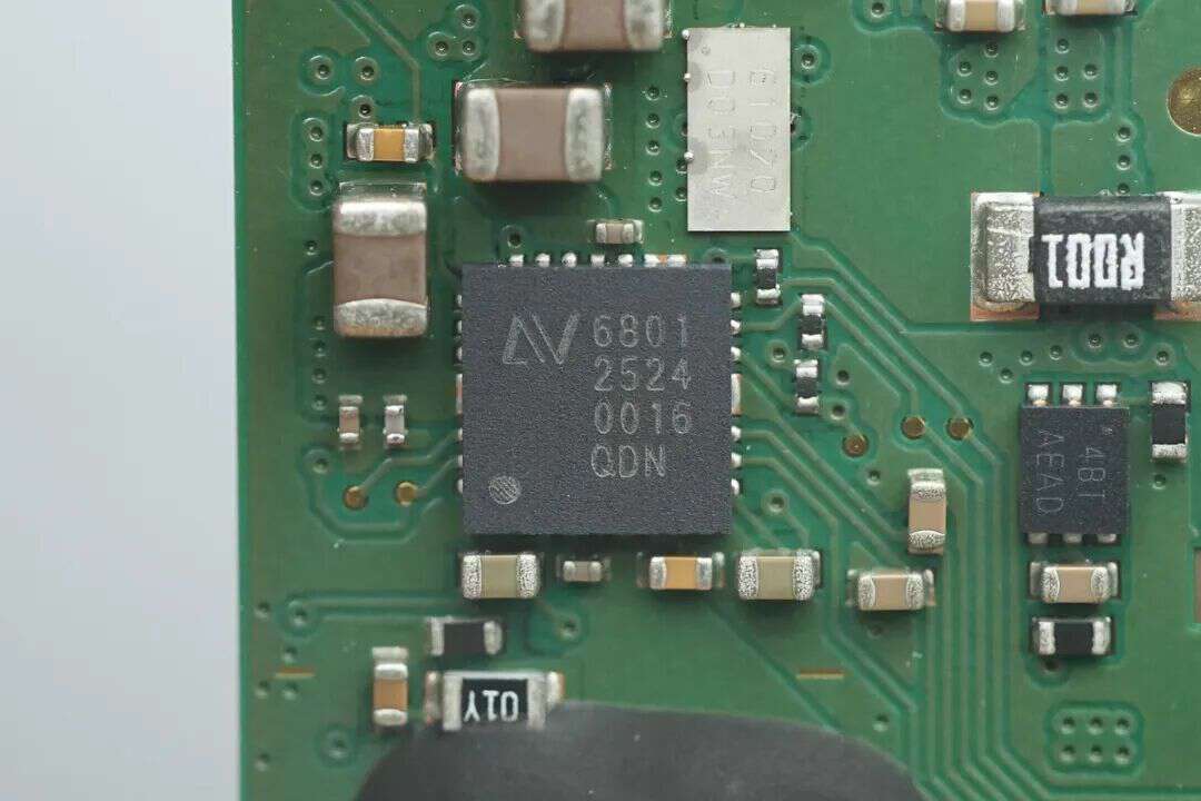
Switching charging chip from NuVolta, model NU6801, is a power management IC integrating charging and discharging functions with three-port path management, supporting a wide range of VBUS voltages.
In charging mode, the maximum input voltage reaches 16 V, and in discharging mode, the maximum output voltage reaches 19 V. It integrates IBUS, IBAT, IAC, VBUS, VBAT, and NTC signal sampling functions, offering high configurability and compatibility. This significantly reduces the number of external components and PCB footprint. The device is packaged in a QFN30.
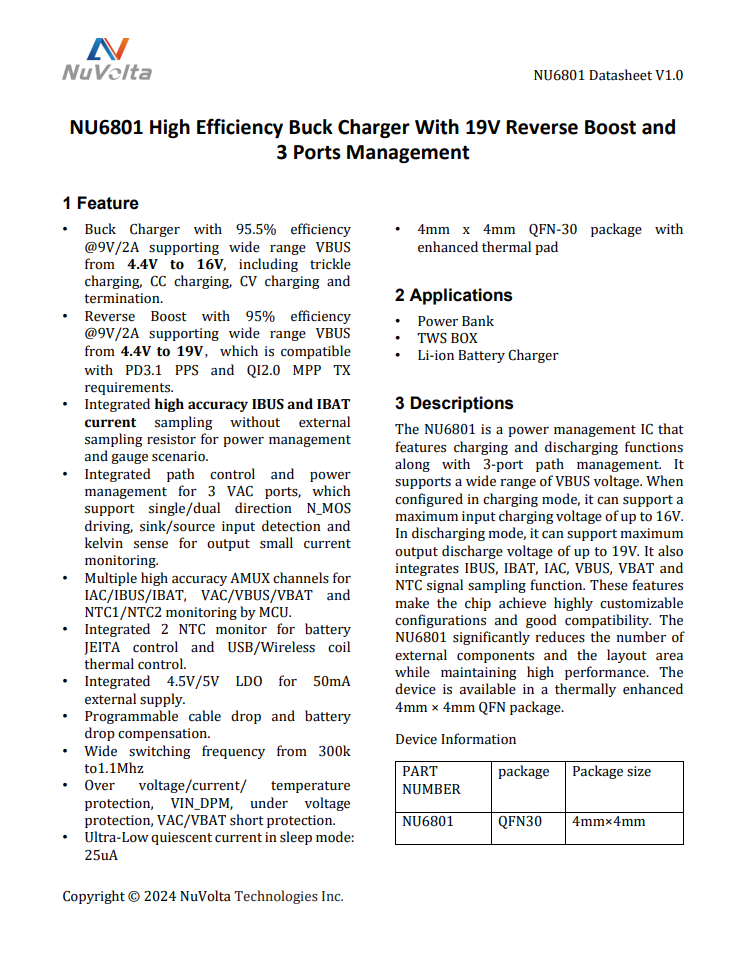
Close-up of a chip marked with "4BT".
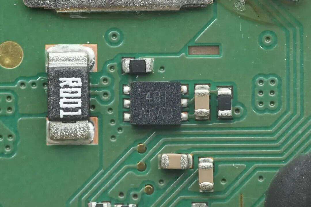
Four buck-boost MOSFETs marked with Q46N03 from Wayon, model WMQ46N03T1, are NMOS devices with a voltage rating of 30 V and an on-resistance of 8 mΩ, packaged in PDFN3030.
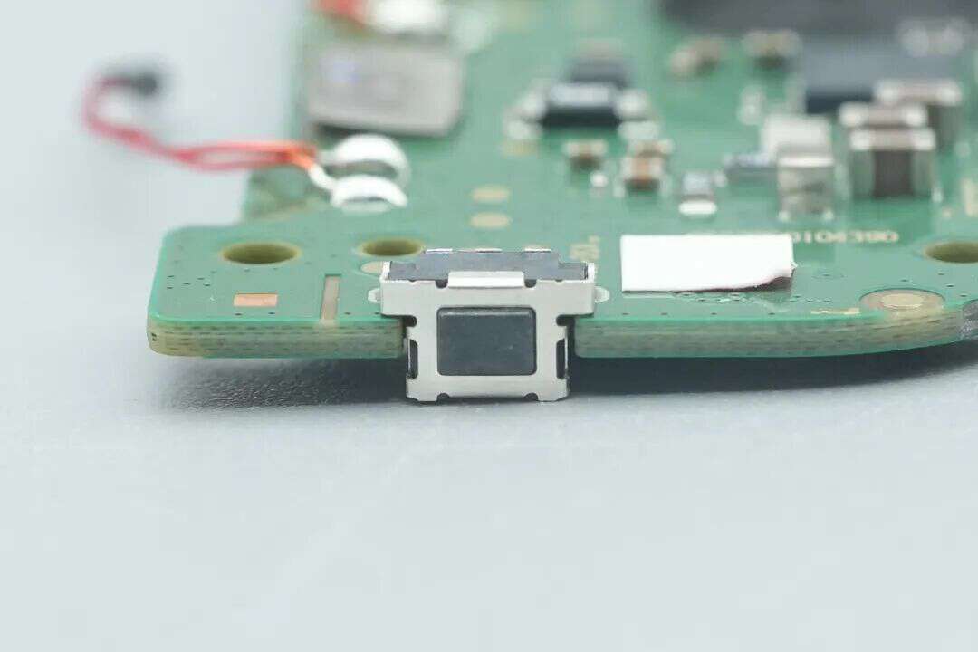
Close-up of the micro switch.
The PCB also features a water ingress indicator sticker.
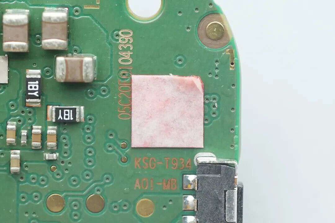
Testing shows that it turns red upon contact with water, facilitating after-sales inspection of damage causes.

Well, those are all components of the Samsung 5000mAh Qi2 Magnetic Wireless Power Bank.
Summary of ChargerLAB
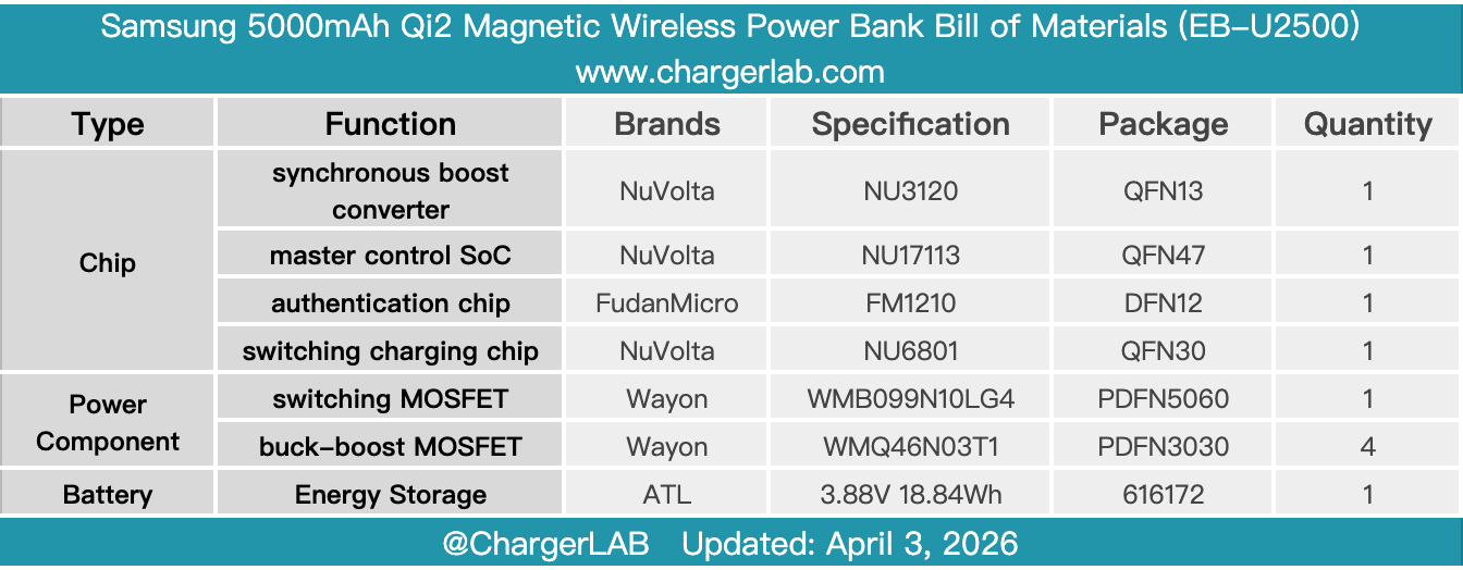
Here is the component list of the Samsung 5000mAh Qi2 Magnetic Wireless Power Bank for your convenience.
The enclosure of this wireless charging power bank features a gray-white skin-friendly material paired with an integrated aluminum alloy stand. Teardown reveals that the materials and workmanship fully reflect Samsung’s consistent high standards. The core circuitry is based on a NuVolta solution, including the NU6801 switching charging IC, NU3120 synchronous boost converter, and NU17113 wireless power bank master control SoC. This integrated solution demonstrates high integration, effectively streamlining external circuitry, while the overall design supports simultaneous charging and discharging as well as Qi2 15 W magnetic wireless fast charging.
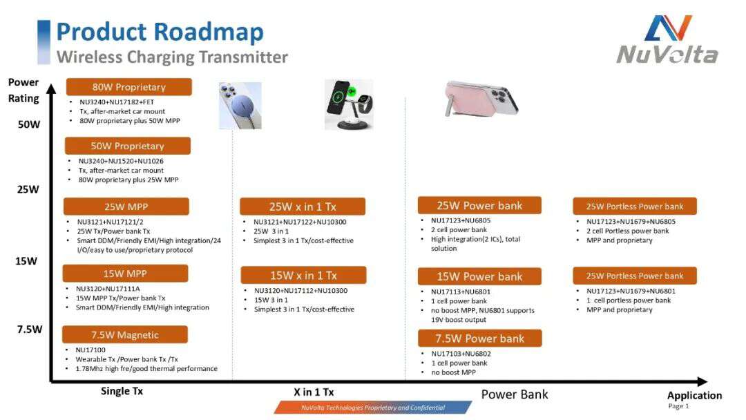
In fact, NuVolta Semiconductor offers a complete product roadmap and solution matrix for wireless charging transmitters. For a comprehensive overview, the following compilation presents NuVolta’s wireless charging transmitter product roadmap and summary tables, covering different power levels, chip combinations, and application scenarios.
The pouch cell is sourced from ATL, and the authentication chip comes from FUDAN, meeting the security encryption requirements of the Qi2 standard. The internal structure is compact and orderly, with both the coil and battery pack equipped with independent thermistors for temperature control. This is complemented by large-area graphite thermal pads, thick thermal silicone pads, and shielding stickers. From the power management IC to thermal design and chip selection, every aspect ensures the device’s stability and safety during everyday use.
Related Articles:
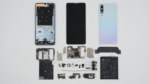
1. Teardown of Huawei P30
2. Teardown of OPPO 50W AirVOOC Magnetic Wireless Charger (OAWV09)
3. Teardown of VMAX AC Power Supply (VT450AB220A)