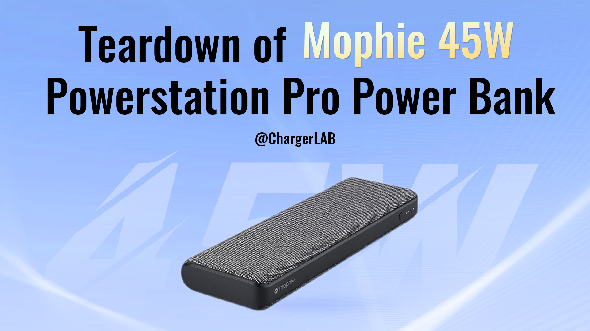
Introduction
On October 21, realme released a new 45W cabled power bank featuring 45W output support and a built-in 20,000 mAh battery. It comes with an integrated charging cable and is available in multiple colors, including white, yellow, and black. Let’s dive into the internal design and build quality of this product.
Product Appearance
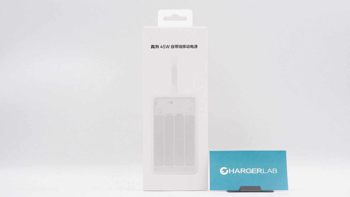
The packaging box features the product name and an image of the device.
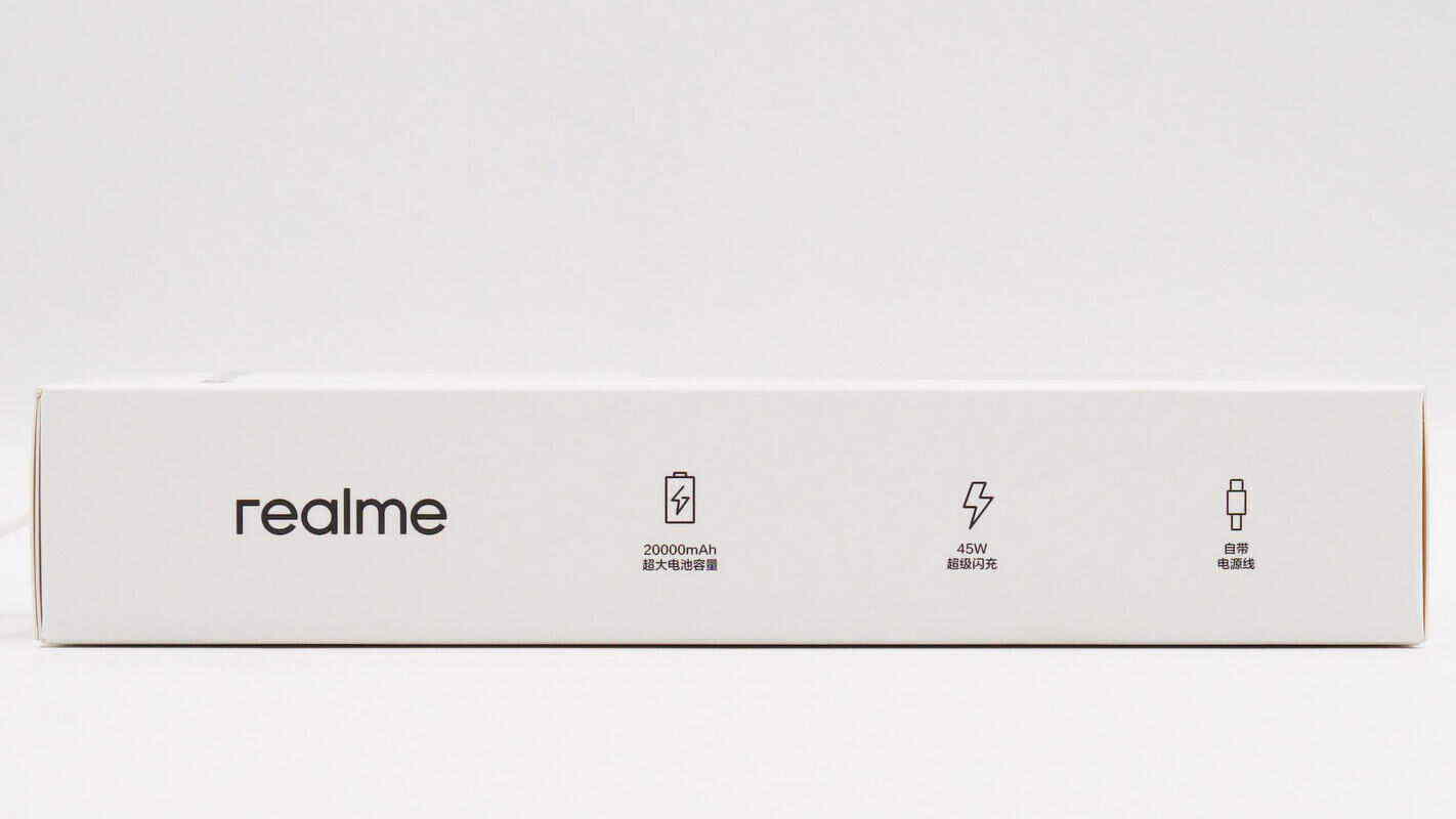
This side displays a black realme logo along with key product highlights.
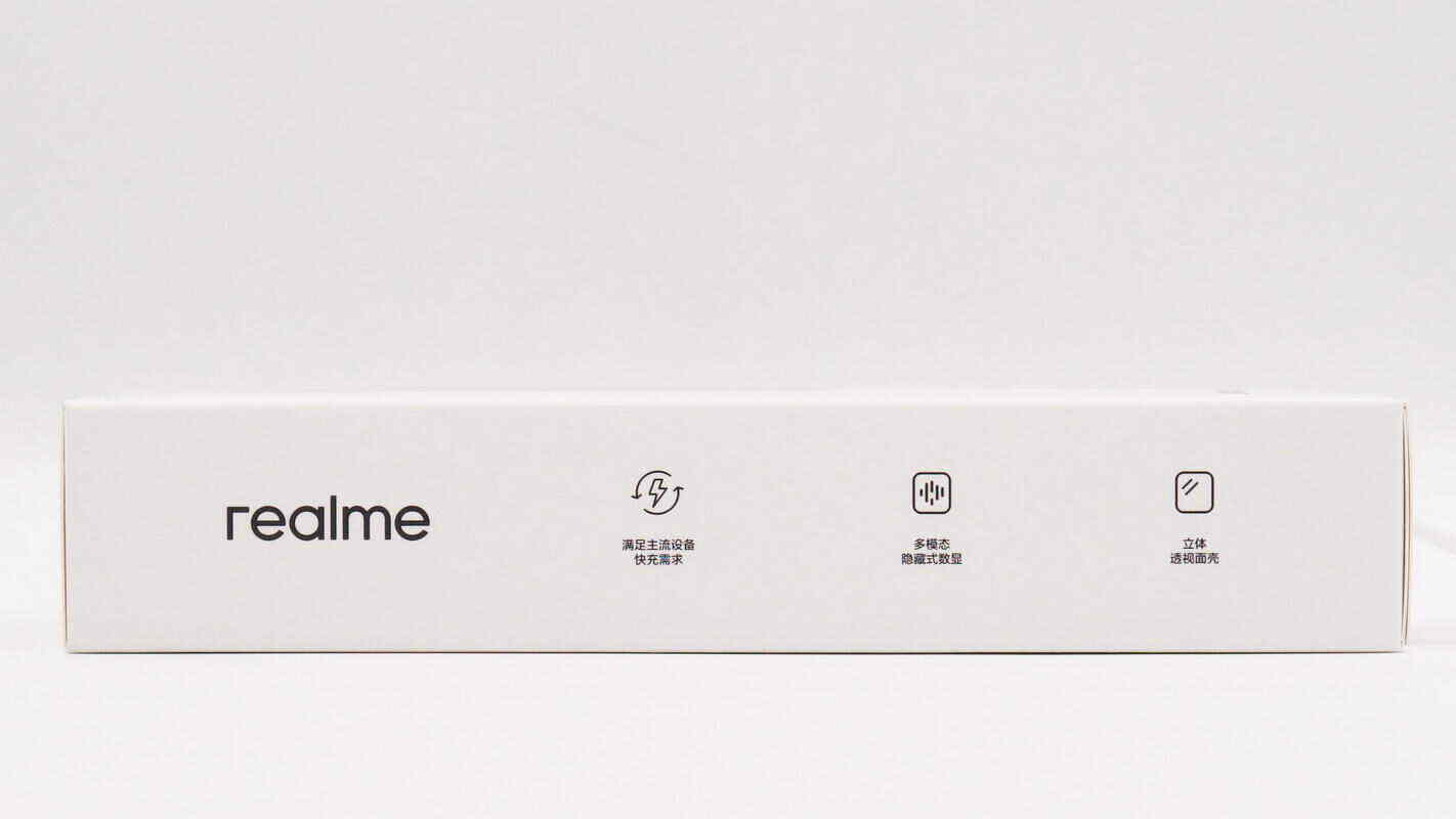
The design on the opposite side is the same.
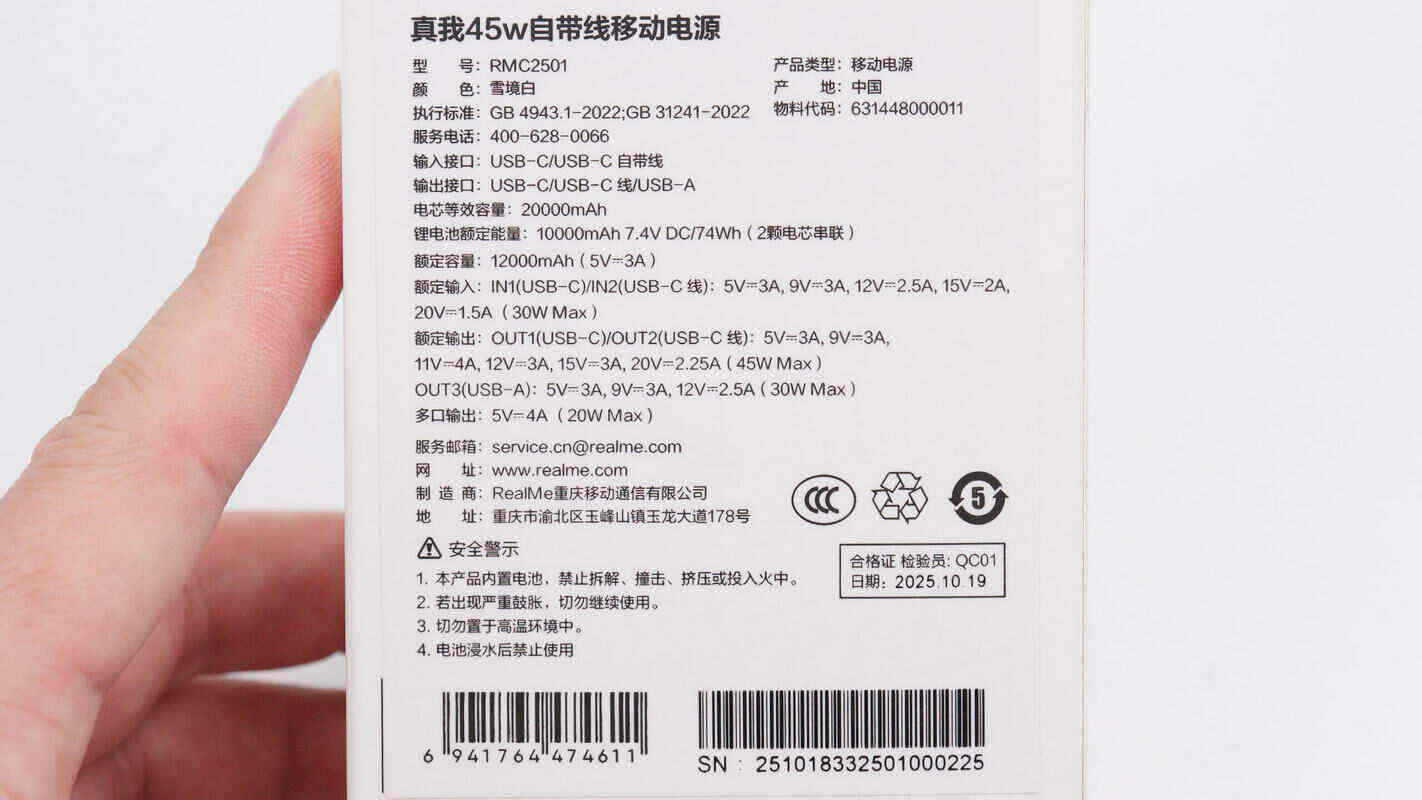
Model: RMC2501
Place of Origin: China
Standards: GB 4943.1-2022; GB 31241-2022
Input Interfaces: USB-C / Built-in USB-C cable
Output Interfaces: USB-C / Built-in USB-C cable / USB-A
Equivalent Cell Capacity: 20,000 mAh
Rated Lithium Battery Energy: 10,000 mAh 7.4 V DC / 74 Wh (two cells in series)
Rated Capacity: 12,000 mAh (5V 3A)
Rated Input:
IN1 (USB-C) / IN2 (Built-in USB-C cable):
5V 3A, 9V 3A, 12V 2.5A, 15V 2A, 20V 1.5A (30W Max)
Rated Output:
OUT1 (USB-C) / OUT2 (Built-in USB-C cable):
5V 3A, 9V 3A, 11V 4A, 12V 3A, 15V 3A, 20V 2.25A (45W Max)
OUT3 (USB-A):
5V 3A, 9V 3A, 12V 2.5A (30W Max)
Multi-port Output:
5V 4A (20W Max)
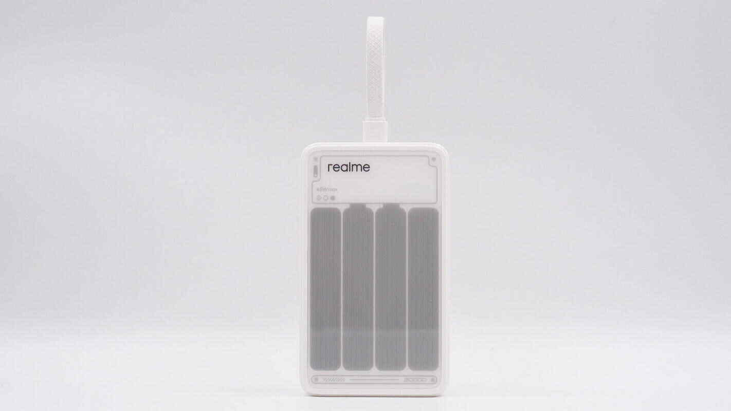
The upper portion of the front side features the realme logo, while four vertically arranged battery cell icons are printed below it.
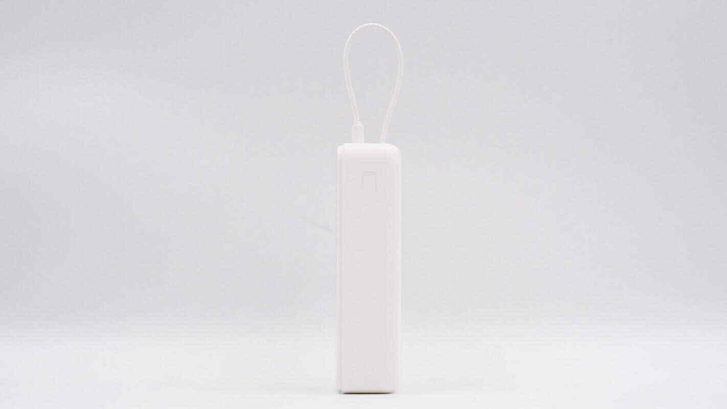
The power button is located on this side.

Pressing the power button causes the front display to show the remaining battery level.
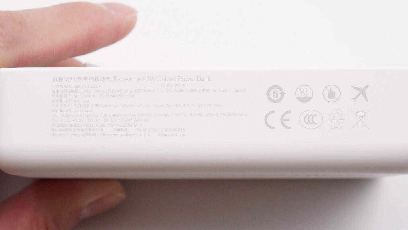
The opposite side displays the specifications and certification marks.
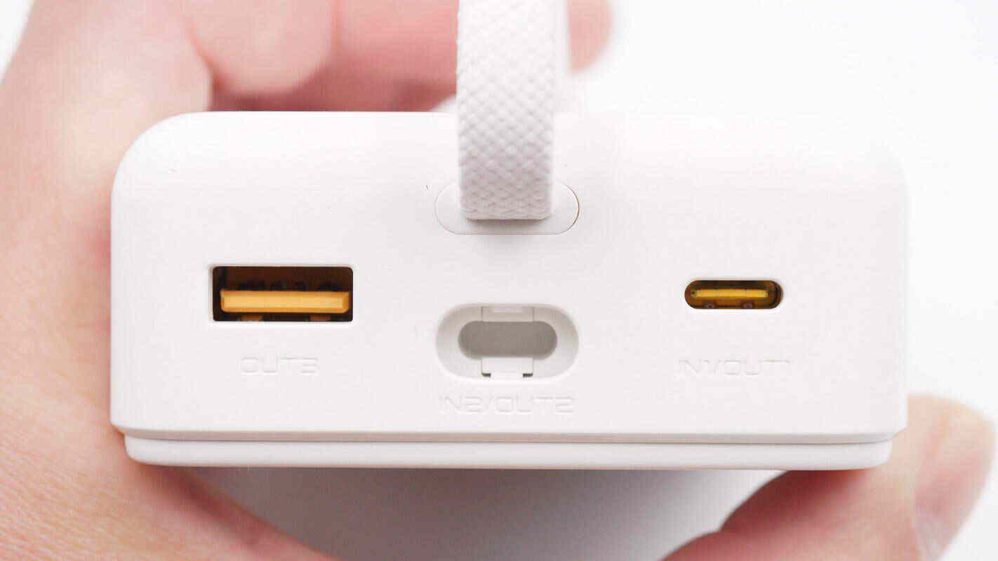
In addition to the built-in USB-C cable, the top features one USB-A and one USB-C port. The center houses a slot for storing the USB-C cable plug.

The built-in cable is flat.
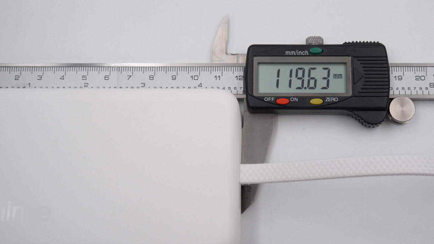
The length of the power bank is about 119.63 mm (4.71 inches).
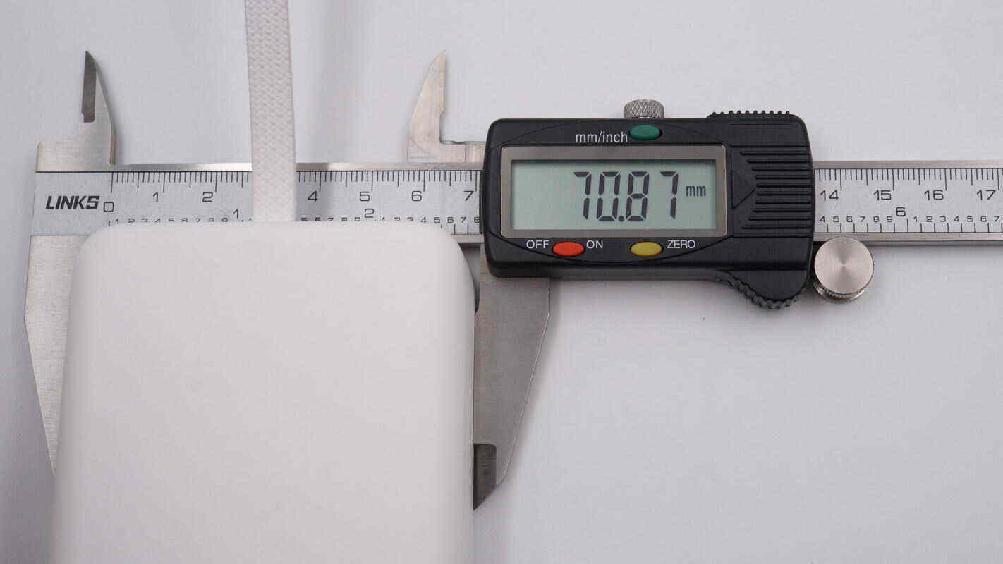
The width is about 70.87 mm (2.79 inches).

The thickness is about 30.85 mm (1.21 inches).

The length of the cable is about 149.91 mm (5.9 inches).

The weight is about 363.9 g (12.84 oz).
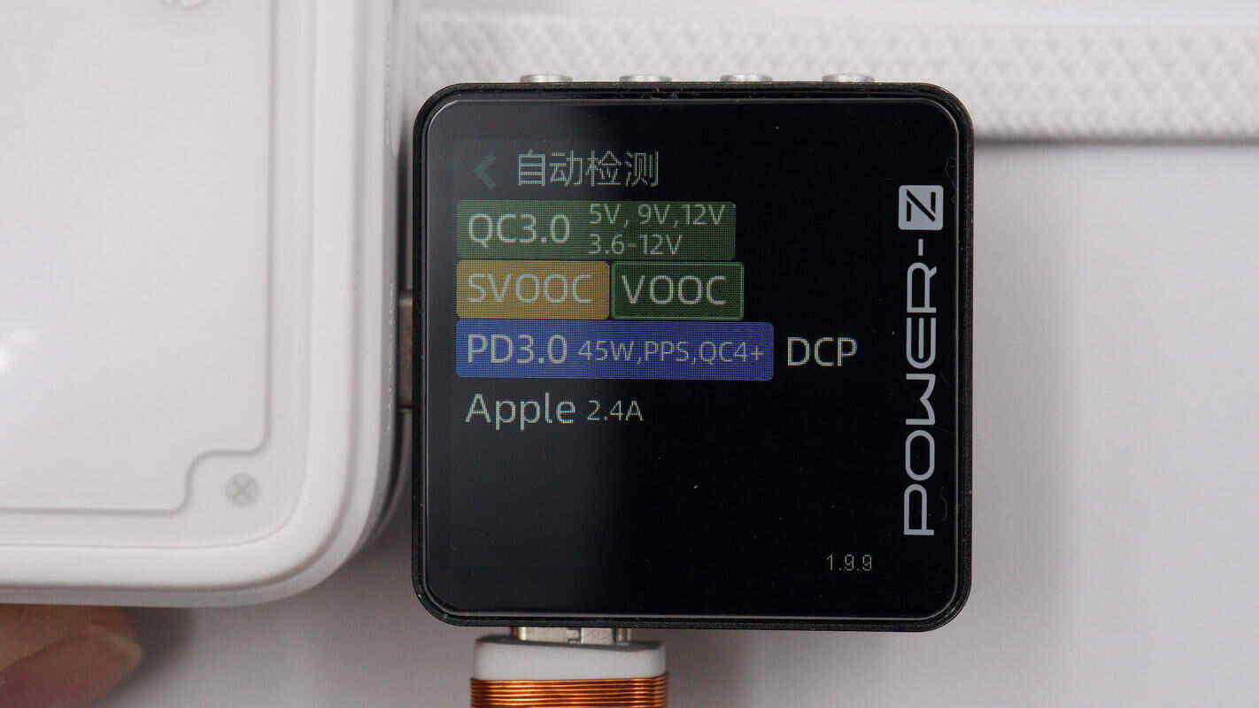
ChargerLAB POWER-Z KM003C shows that the USB-C port supports QC3.0/4+, SVOOC, VOOC, PD3.0, DCP, and Apple 2.4A charging protocols.
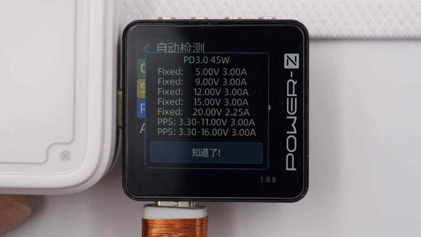
And it has five fixed PDOs of 5V3A, 9V3A, 12V3A, 15V3A, and 20V2.25A. It has two sets of PPS, which are 3.3-11V/3A and 3.3-16V/3A.
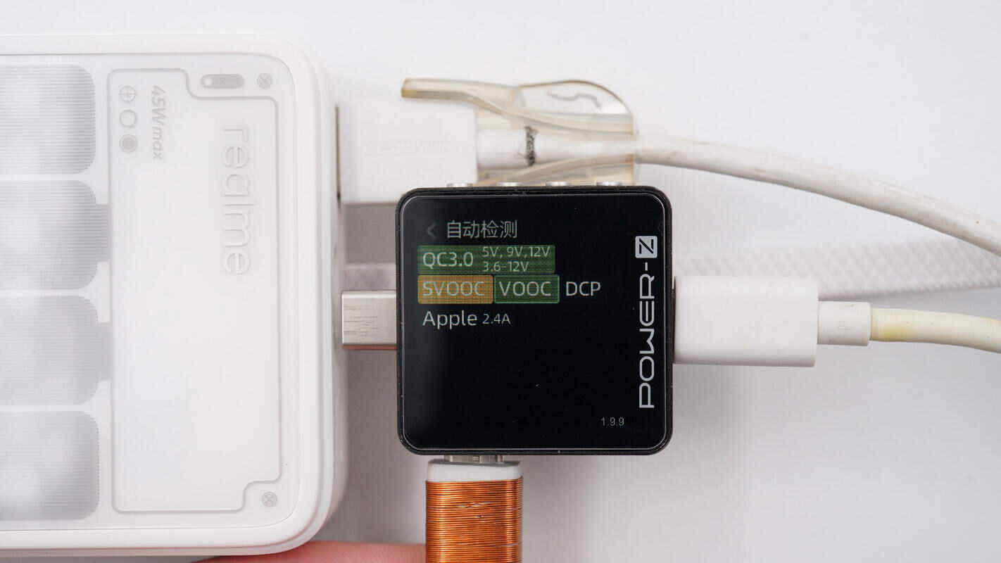
The USB-A port supports QC3.0, SVOOC, VOOC, DCP, and Apple 2.4A charging protocols.
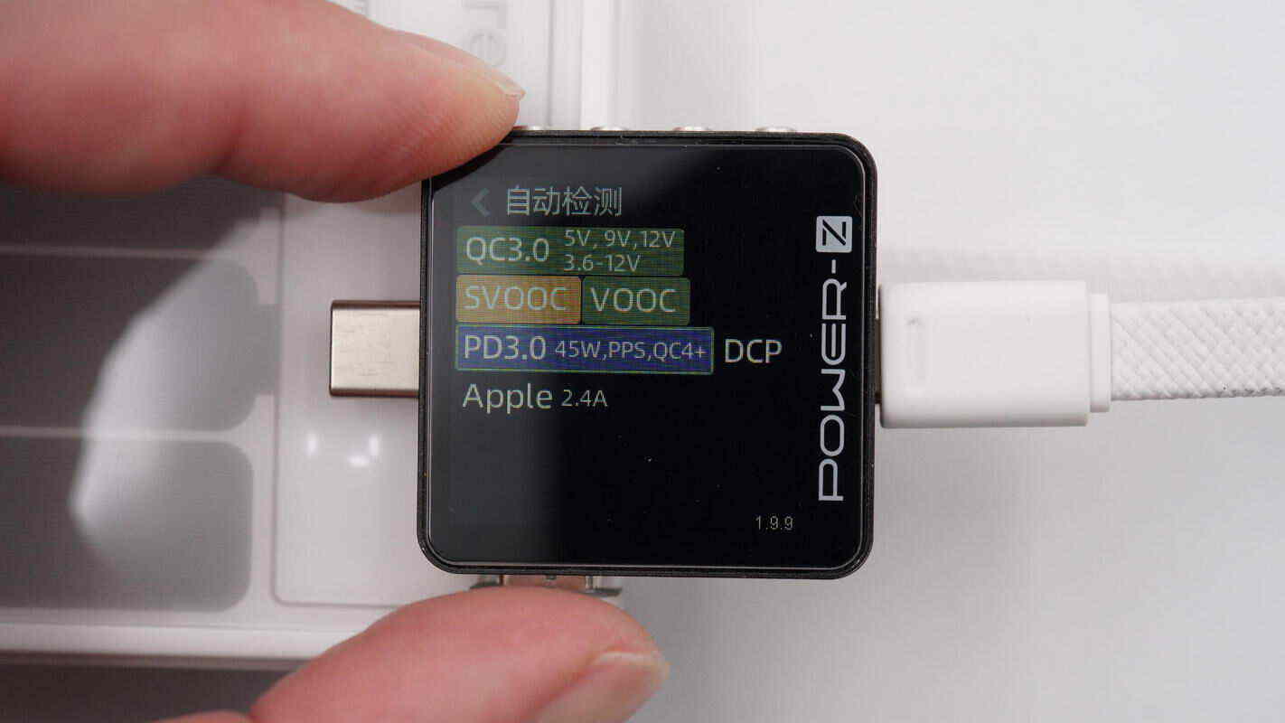
The USB-C cable supports QC3.0/4+, SVOOC, VOOC, PD3.0, DCP, and Apple 2.4A charging protocols.
Teardown
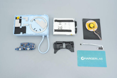
Next, let's take it apart to see its internal components and structure.
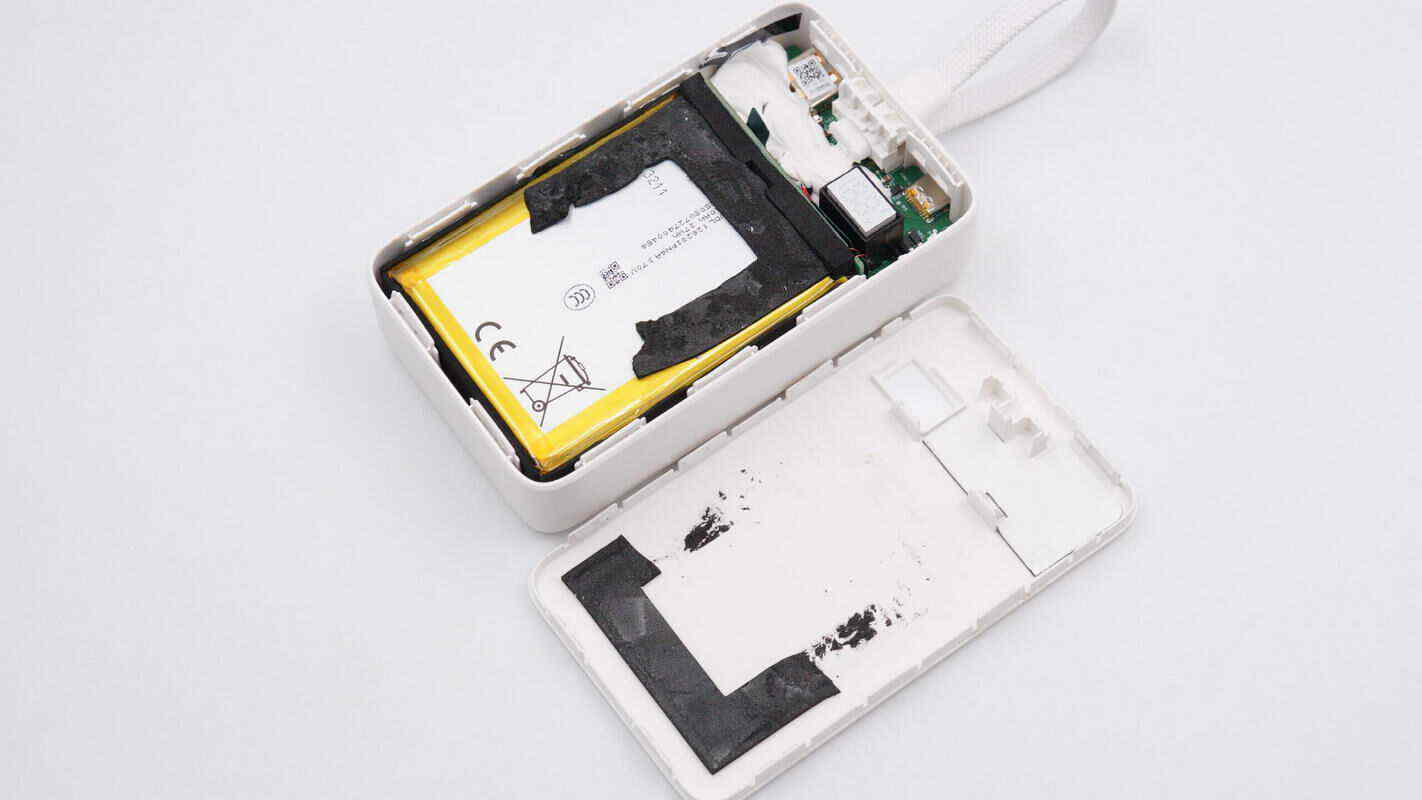
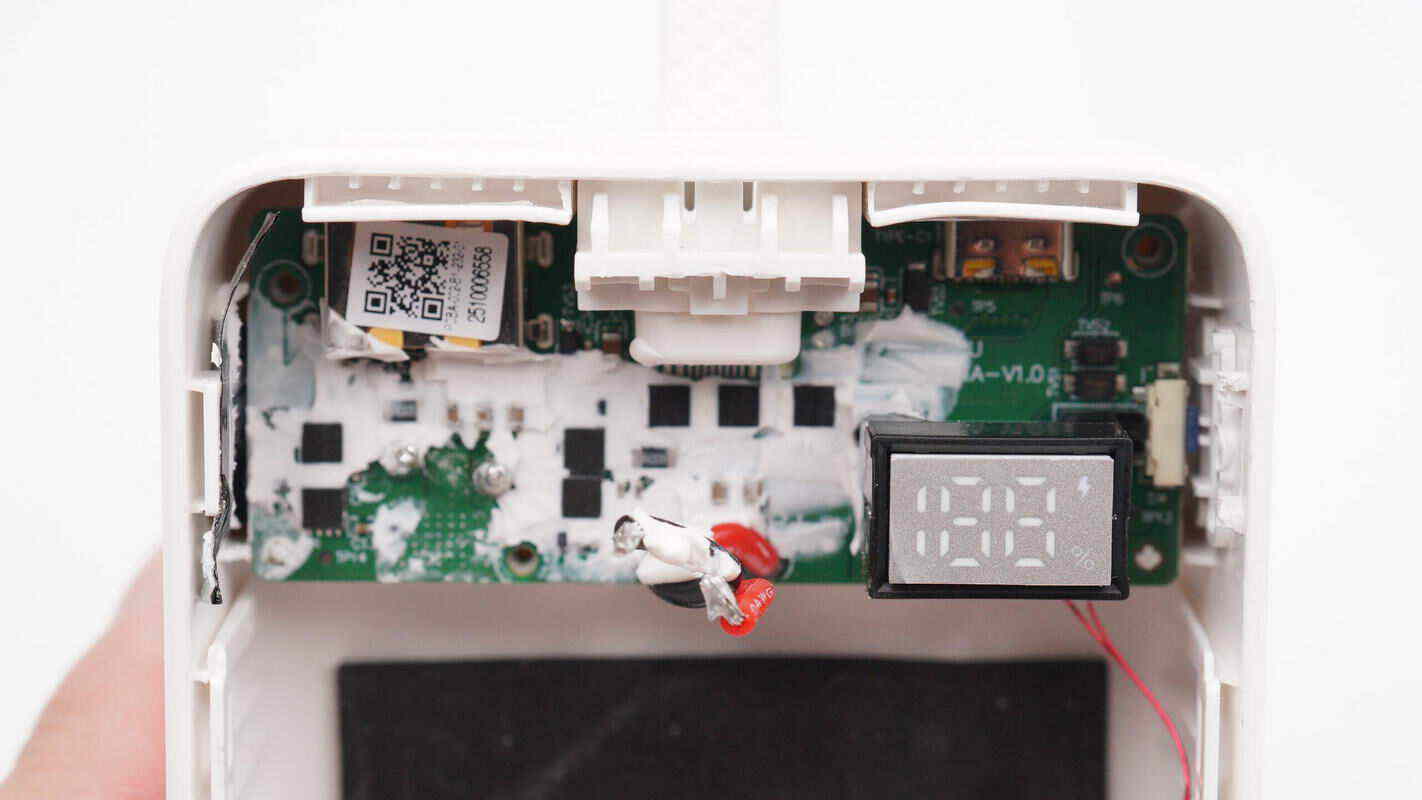
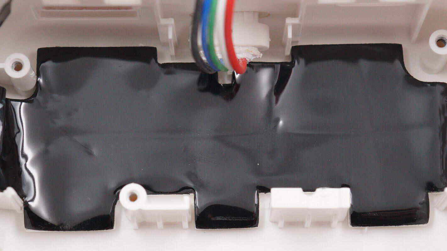
The front panel can be pried open along the seams, where it is secured by clips. Black cushioning foam is placed between the battery pack and the panel.
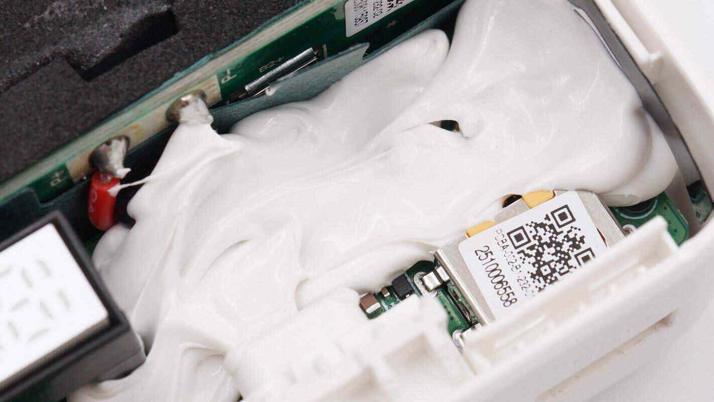
A large area of white thermal paste is applied to the PCBA module region.
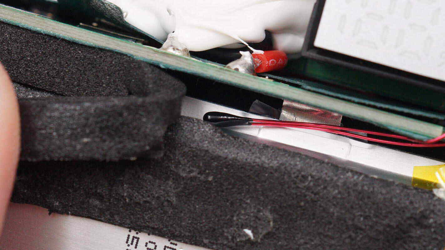
The battery pack is equipped with a thermistor, which is secured in place with foam.
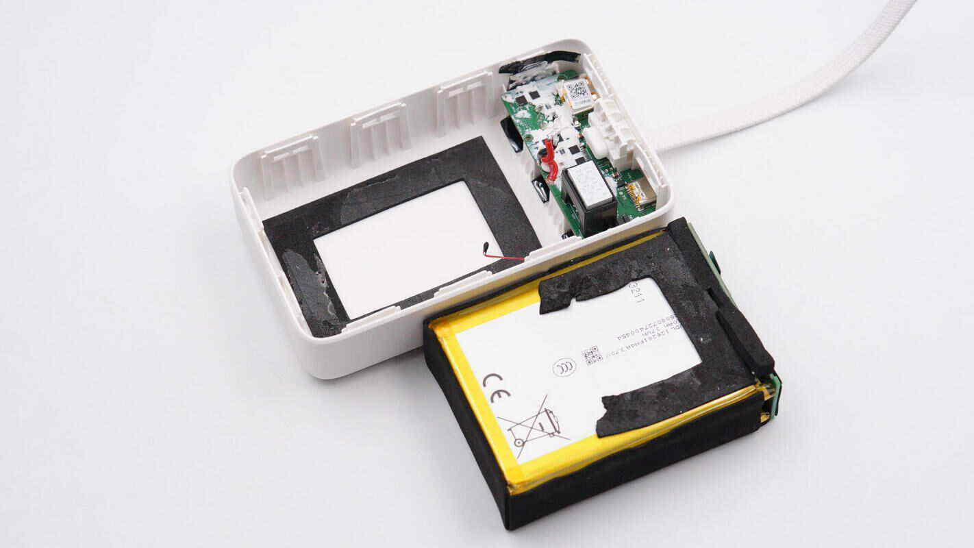
Remove the battery pack.
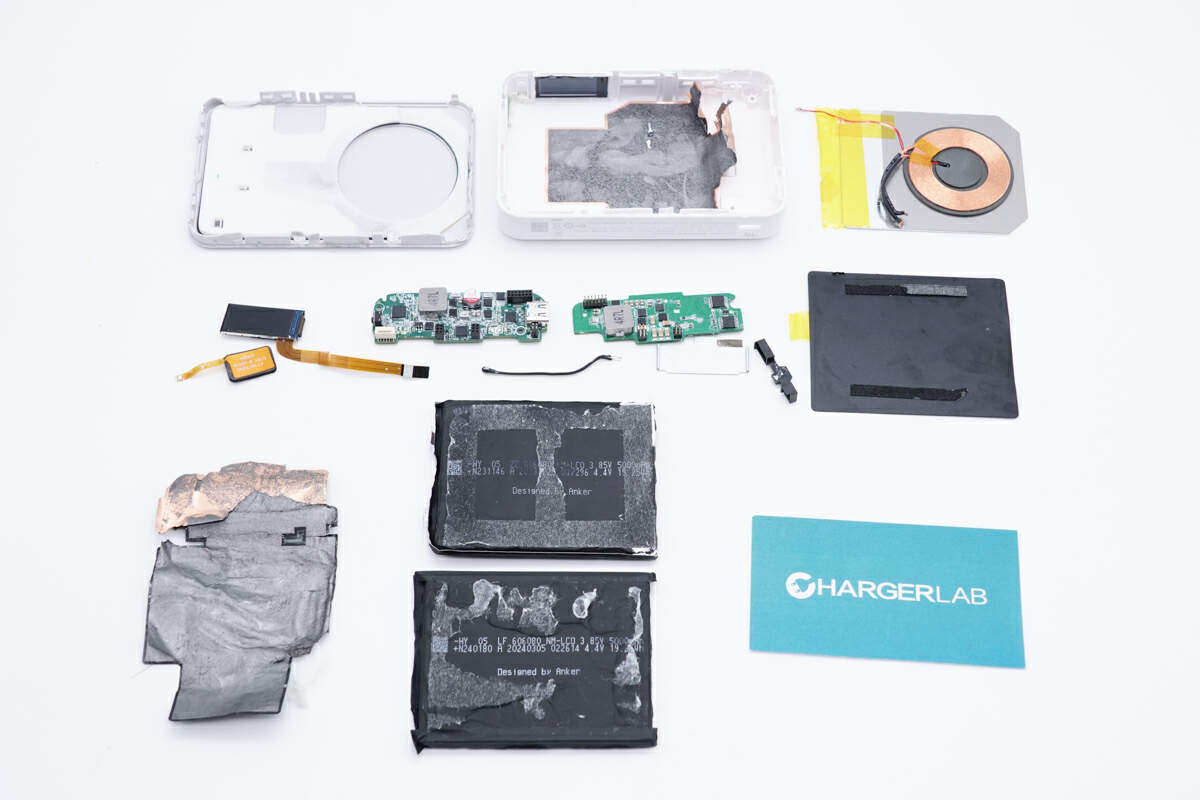
Foam padding is applied around all sides of the battery pack.
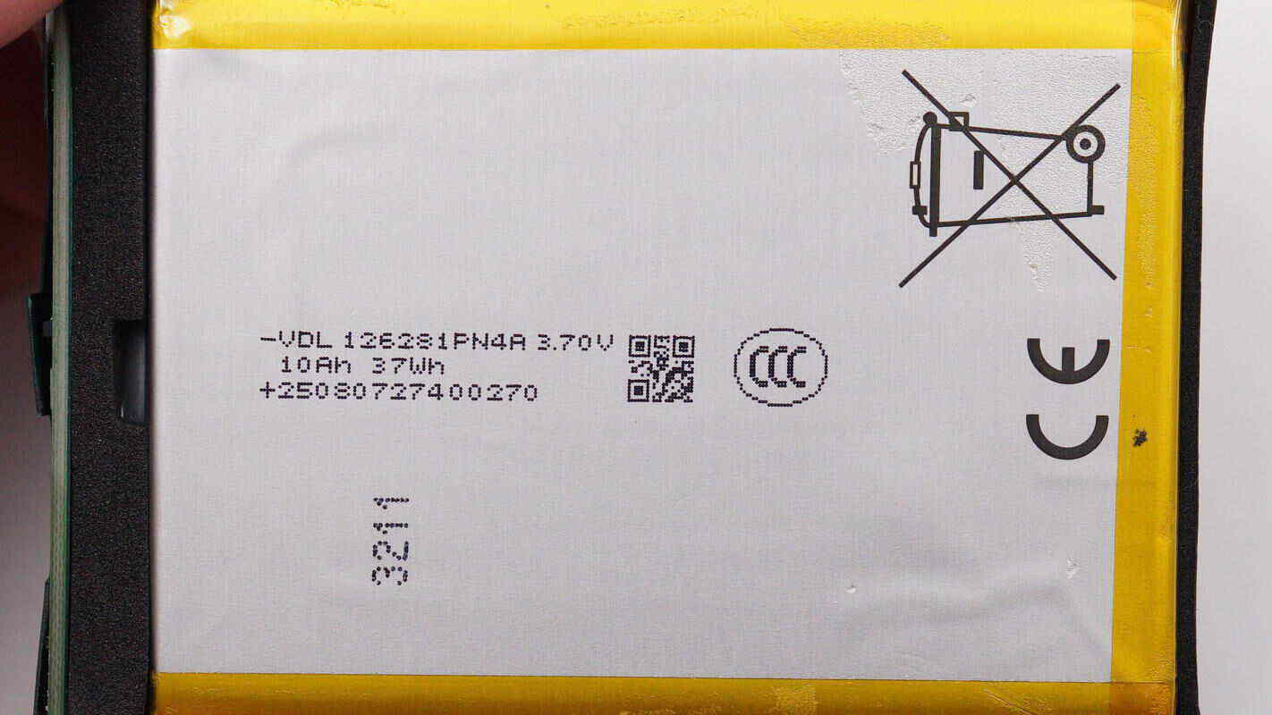
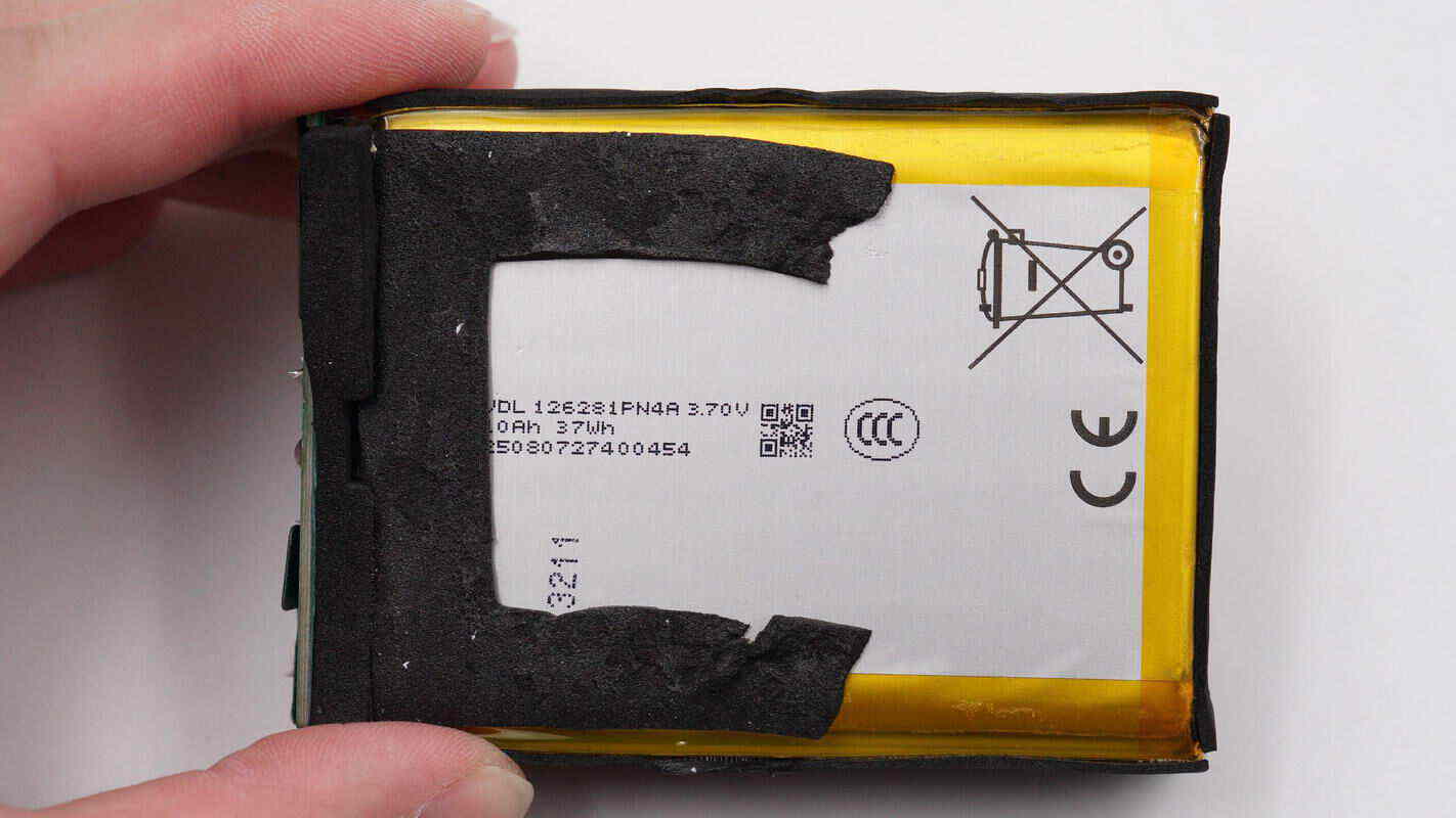
The battery cells are sourced from VDL, model 126281PN4A, with a rated energy of 37Wh, rated voltage of 3.7V, and rated capacity of 10Ah (10000 mAh). This cell has already obtained 3C certification.
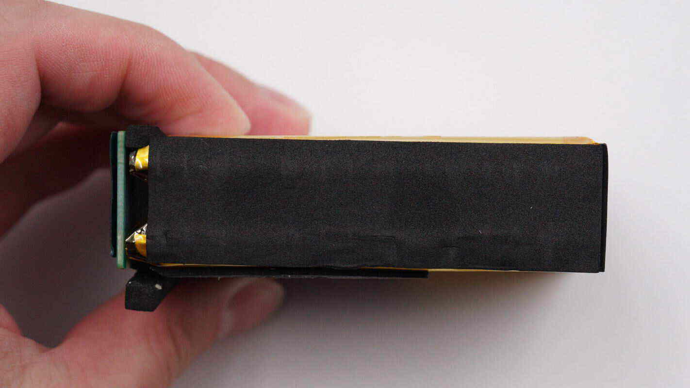
The side of the battery pack is covered with black foam.
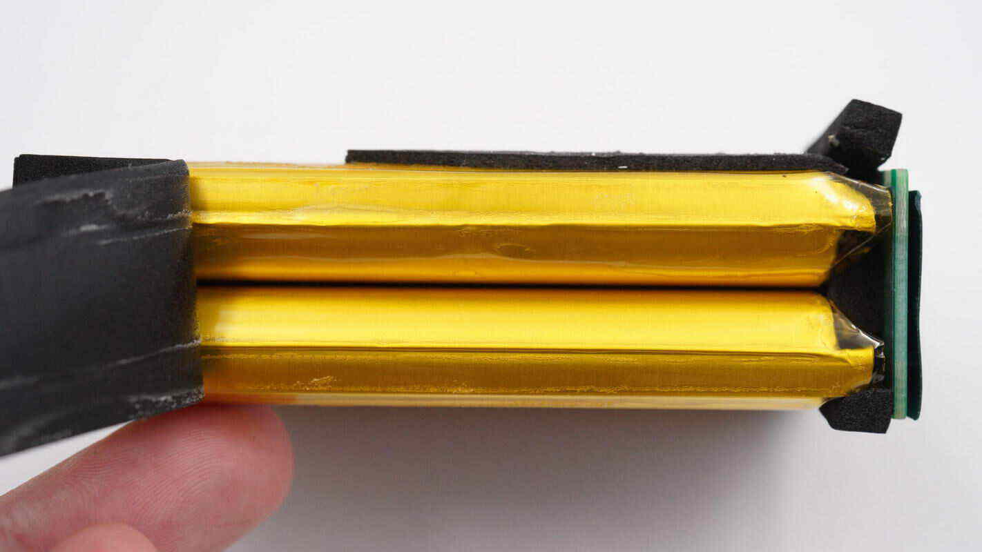
The battery pack consists of two soft-pack cells connected in series.
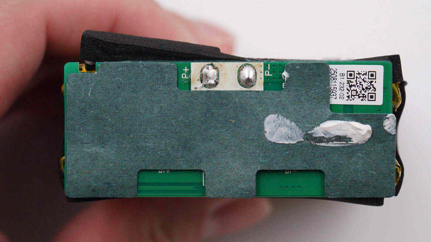
The battery protection PCB is insulated with Kapton tape.
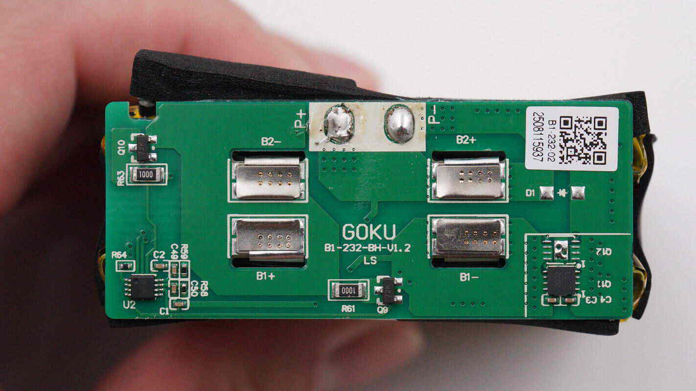
Remove the Kapton tape. The battery protection PCB reveals a battery protection chip, battery protection MOSFETs, and a balancing circuit.
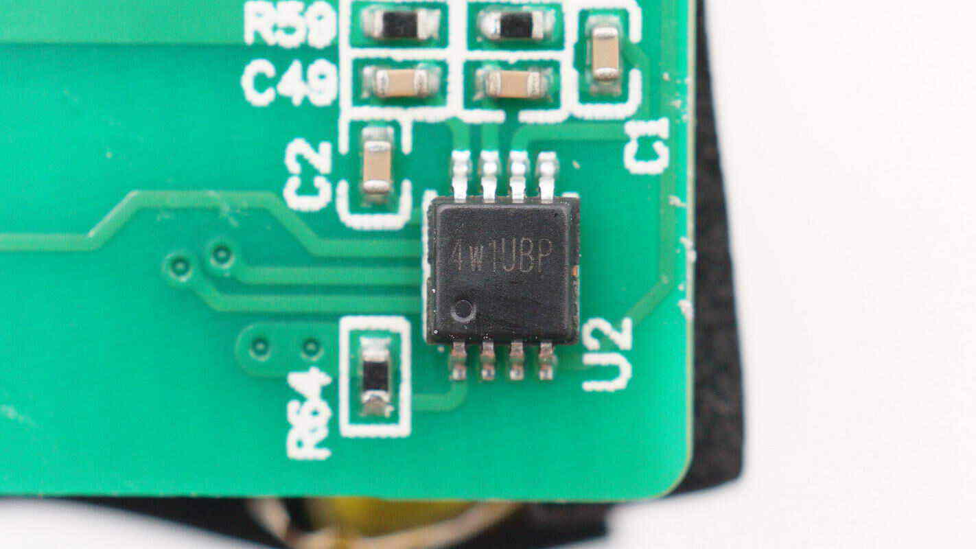
The battery protection chip is marked with 4w1UBP.
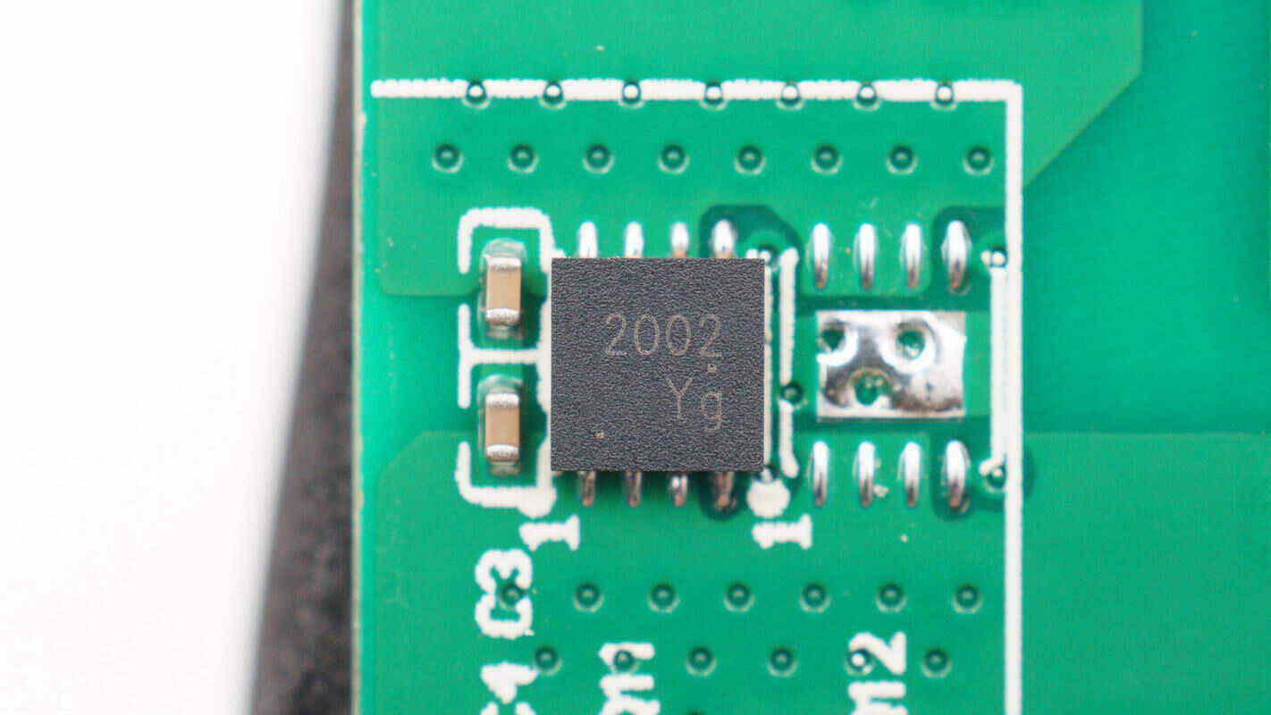
The battery protection MOSFET is marked with 2002, model LT2002EFOB, sourced from Leadteck. It is a dual NMOS with a voltage rating of 20 V and comes in a TDFN 3×3–8L package.
Remove the white thermal paste from the PCBA module.
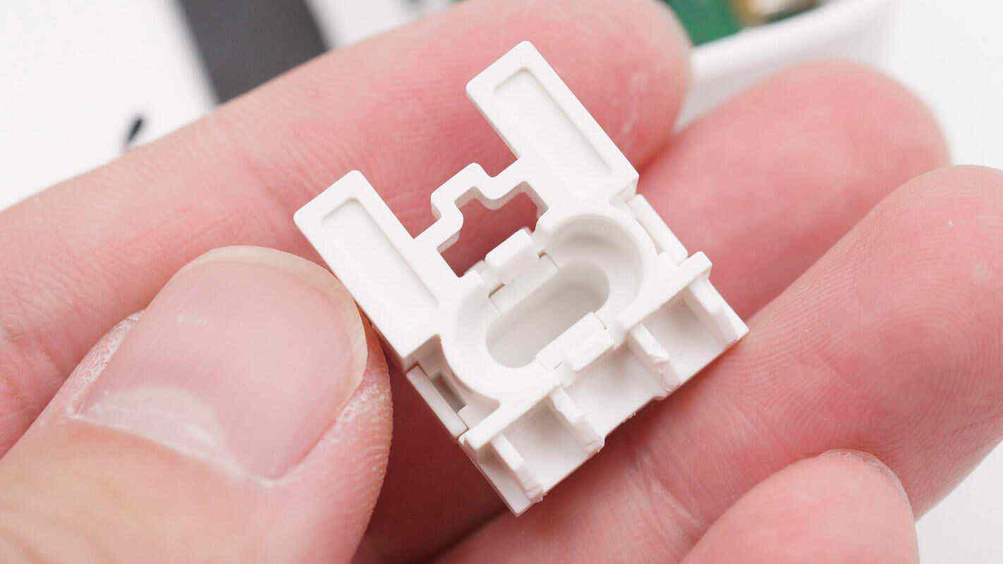
Close-up of the storage bracket for the USB-C plug.
The built-in USB-C cable is connected to the PCB via a detachable ribbon cable.
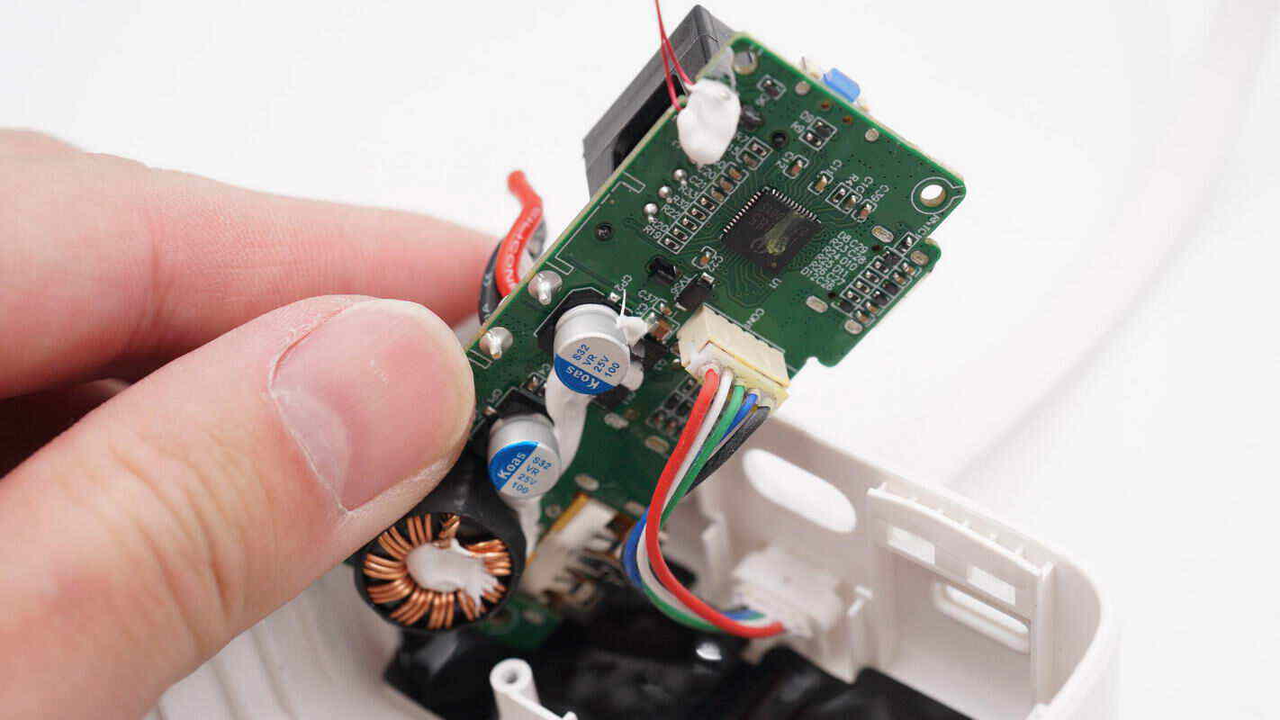
A large thermal pad is placed on the lower layer of the PCBA.
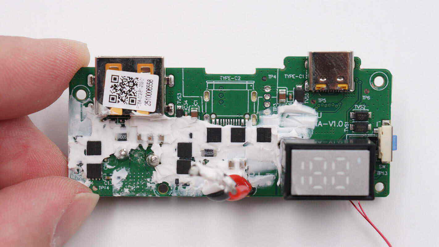
The front side of the PCB features synchronous buck-boost MOSFETs, VBUS MOSFETs, TVS diodes, a USB-A socket, and a USB-C socket.
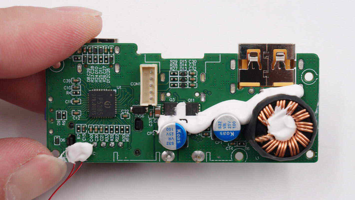
The back side houses the power bank SoC, VBUS MOSFETs, solid capacitors, and a buck-boost inductor.
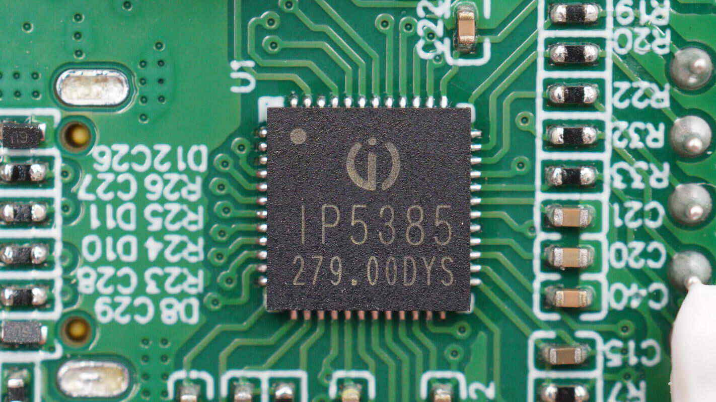
The power bank SoC is from Injoinic, model IP5385. It supports fast-charging protocols such as PD3.0, PPS, AFC, and FCP, and integrates multiple functions, including synchronous bidirectional buck-boost driving, lithium battery charging management, and battery level indication, providing a complete power solution for fast-charging power banks.
It can simultaneously support two USB-A ports, one USB-C port, and one Lightning port. Any single port can independently deliver fast charging, while using two or more output ports at the same time limits operation to 5 V input/output. Thanks to the high integration and rich functionality of the IP5385, very few external components are needed in applications—only a single inductor is required to achieve bidirectional buck-boost functionality—effectively reducing the overall size of the solution and lowering BOM costs.
The IP5385 supports 2 to 4 series-connected cells, and its synchronous buck-boost system can deliver up to 65 W of input and output power. It automatically enters sleep mode under light load and comes in a QFN48 package.
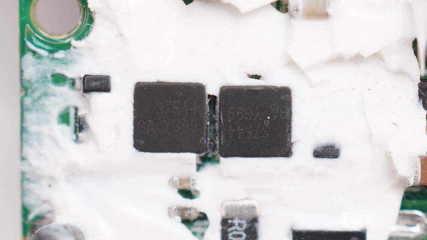
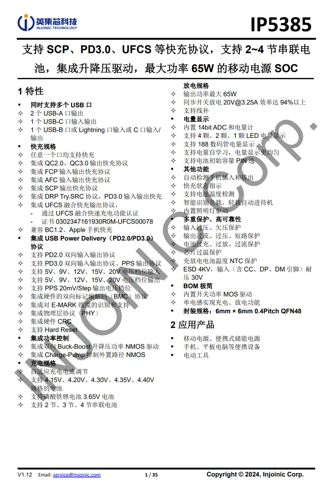
The synchronous buck-boost MOSFETs are marked S7544, sourced from Leadteck, model LTS7544FL. They have a voltage rating of 30 V and come in a PDFN 3×3–8L package.
The other two synchronous buck-boost MOSFETs are also LTS7544FL, forming a set of four MOSFETs that make up a full four-switch synchronous buck-boost power stage.
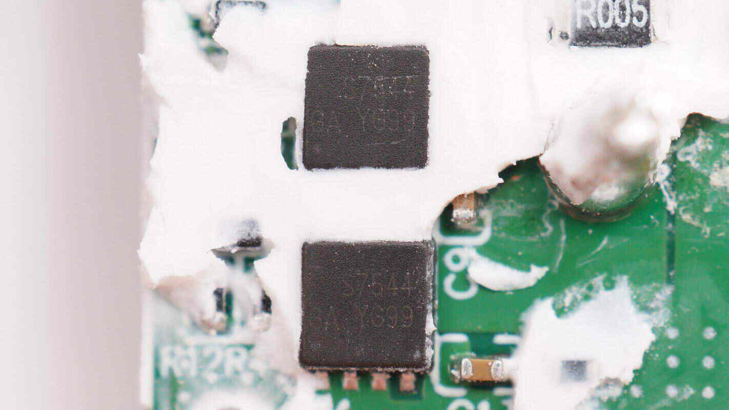
The buck-boost inductor paired with the four synchronous buck-boost MOSFETs is insulated and protected with a heat-shrink tube.
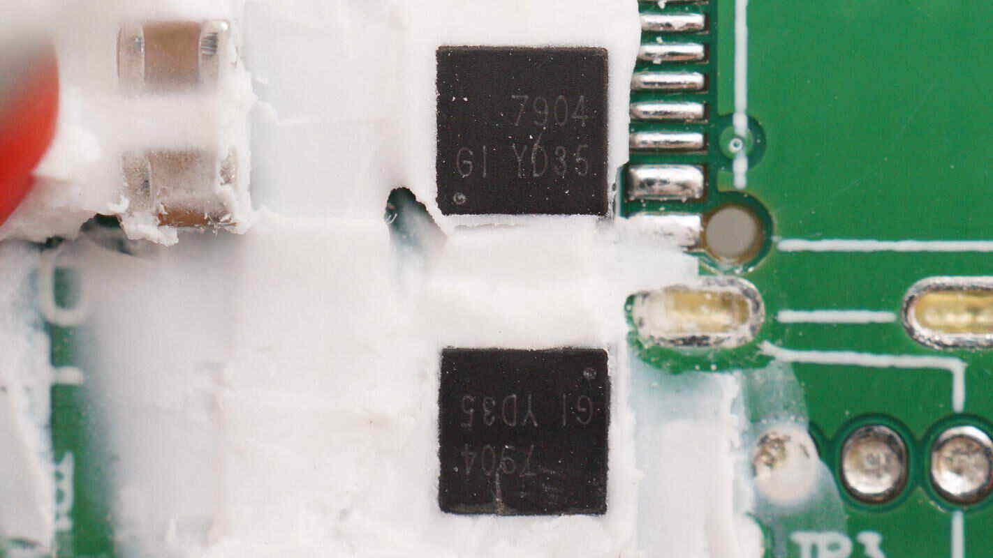
The VBUS MOSFETs used for the USB-C port are marked 7904, sourced from Leadteck, model LT7904FL‑X. They have a voltage rating of 30 V and come in a PDFN 3×3–8L package.
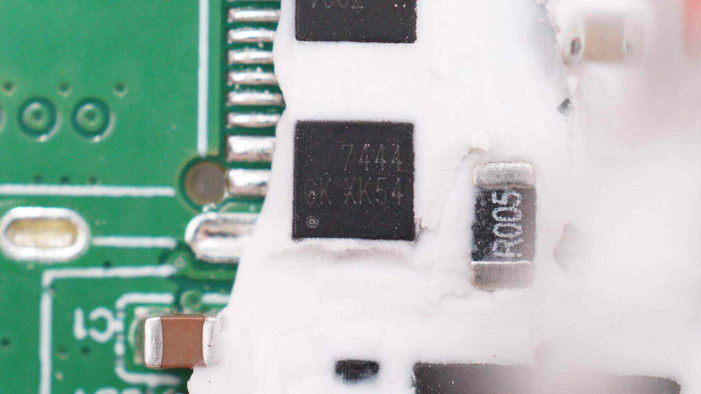
The VBUS MOSFET used for the USB-A port is marked 7444, sourced from Leadteck, model LT7444FL‑X. It has a voltage rating of 30 V and comes in a PDFN 3×3–8L package.
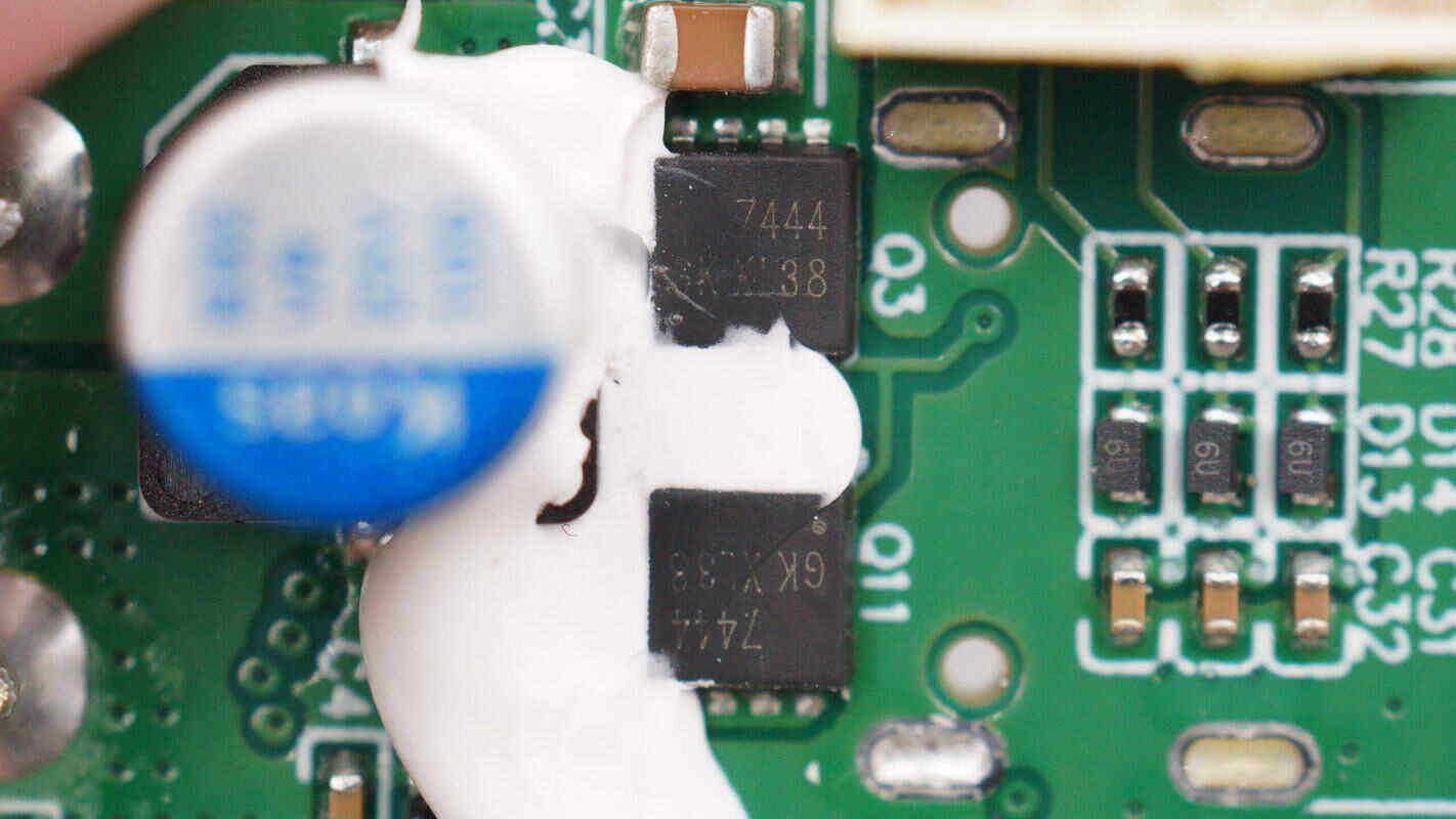
The VBUS MOSFETs for the built-in USB-C cable are also from Leadteck, model LT7444FL‑X, with a voltage rating of 30 V and a PDFN 3×3–8L package.
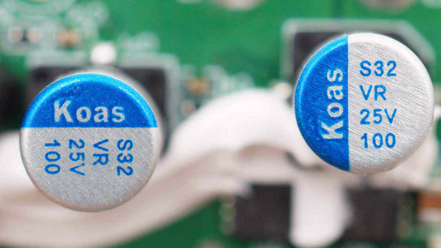
The two solid capacitors are from Koshin, rated at 25 V and 100 μF.
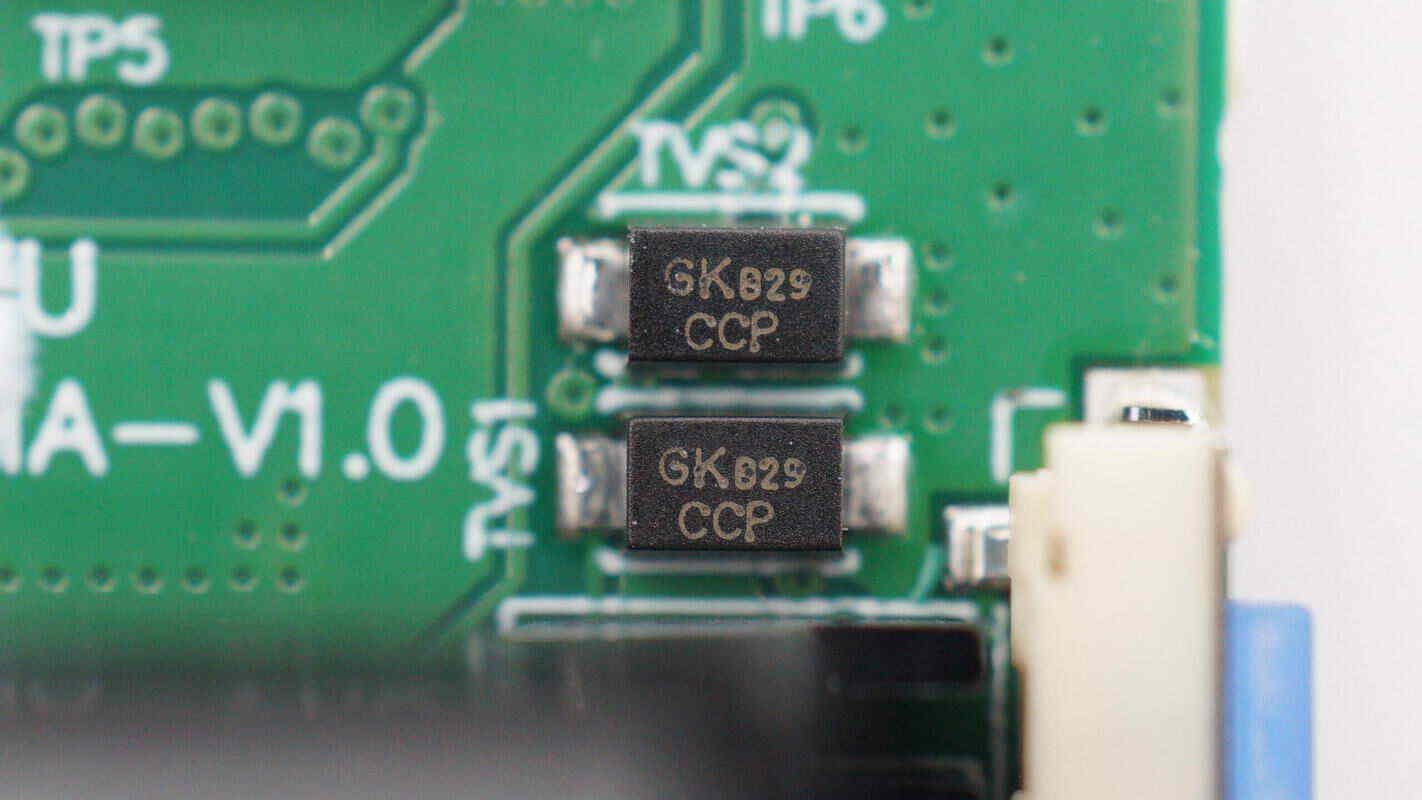
The two TVS diodes are marked GK829.
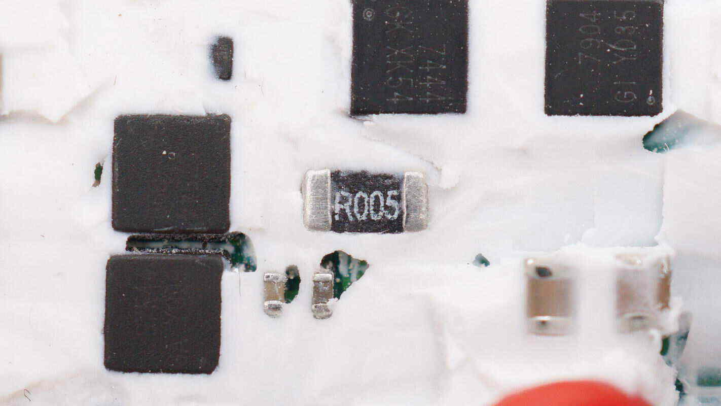
Close-up of the 5mΩ current sampling resistor.
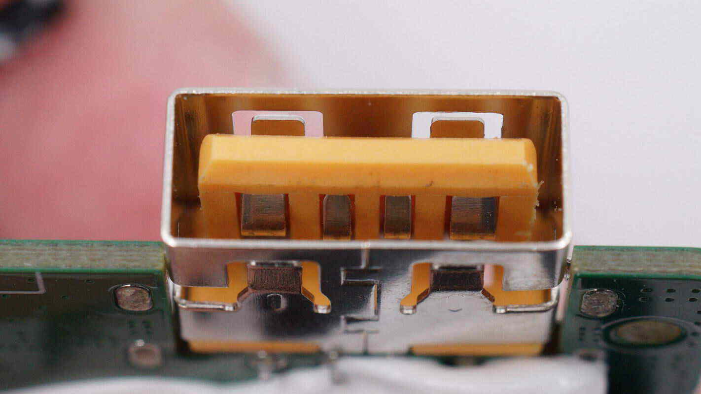
The USB-A port is through-hole soldered and uses a yellow plastic sheet.
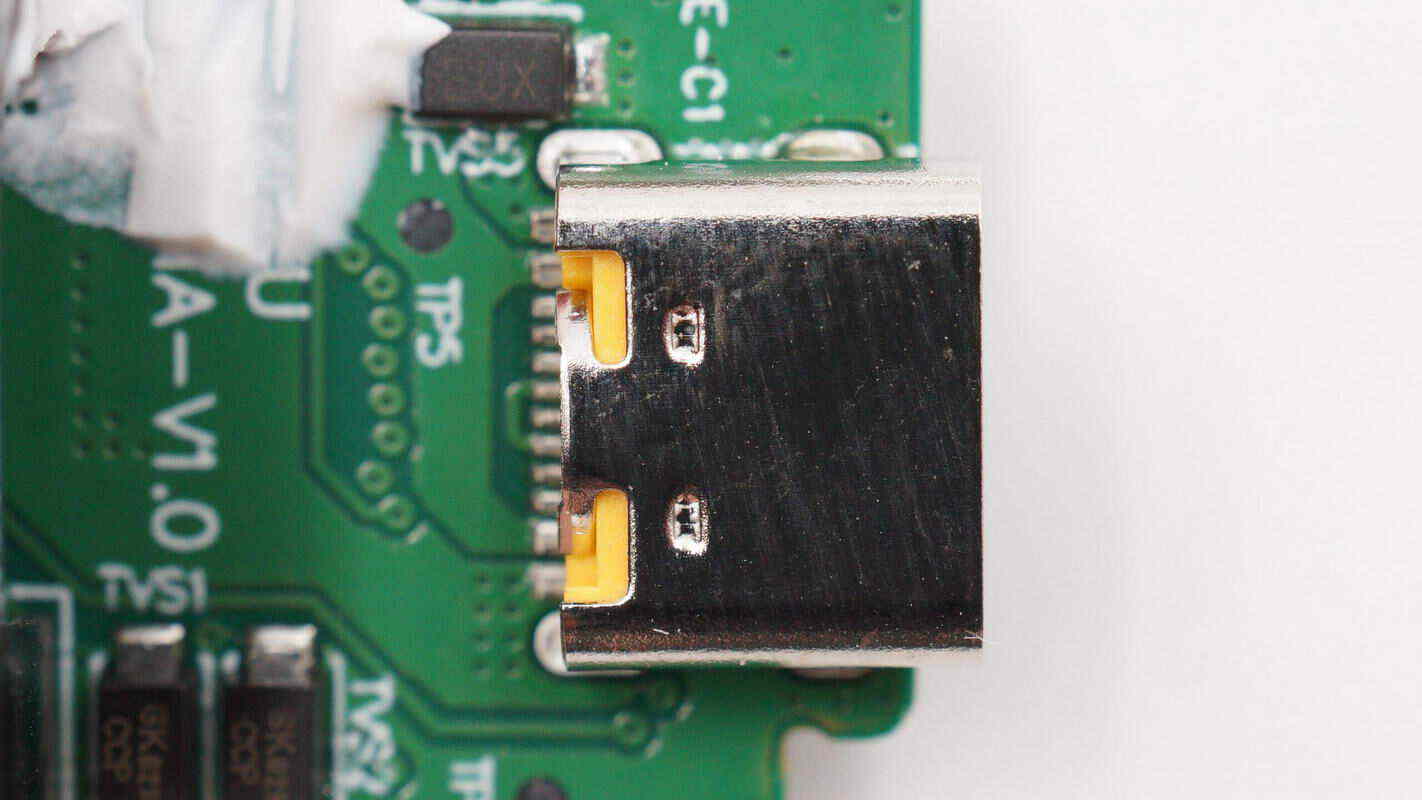
The USB-C port also uses a yellow plastic sheet.
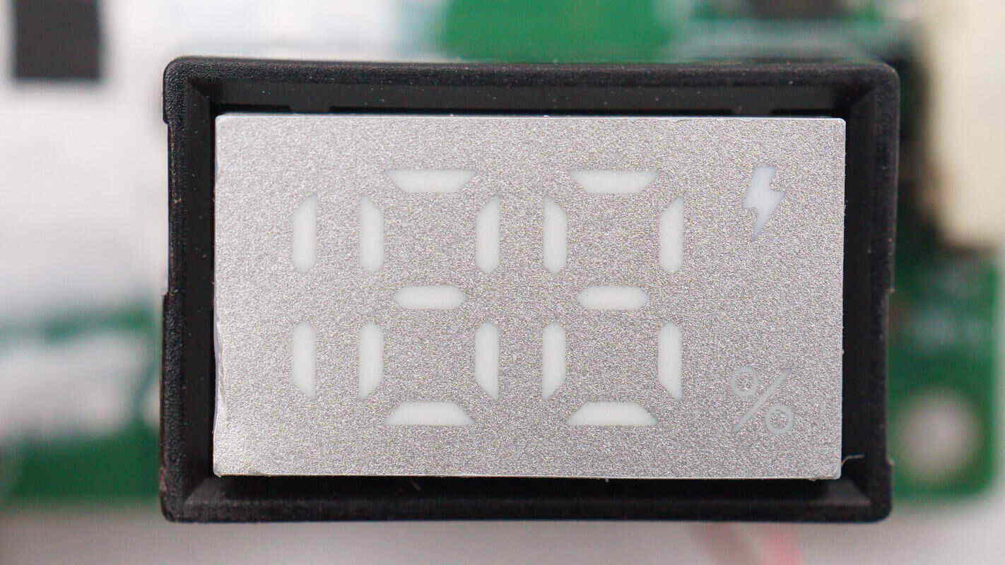
Close-up of the digital display module.
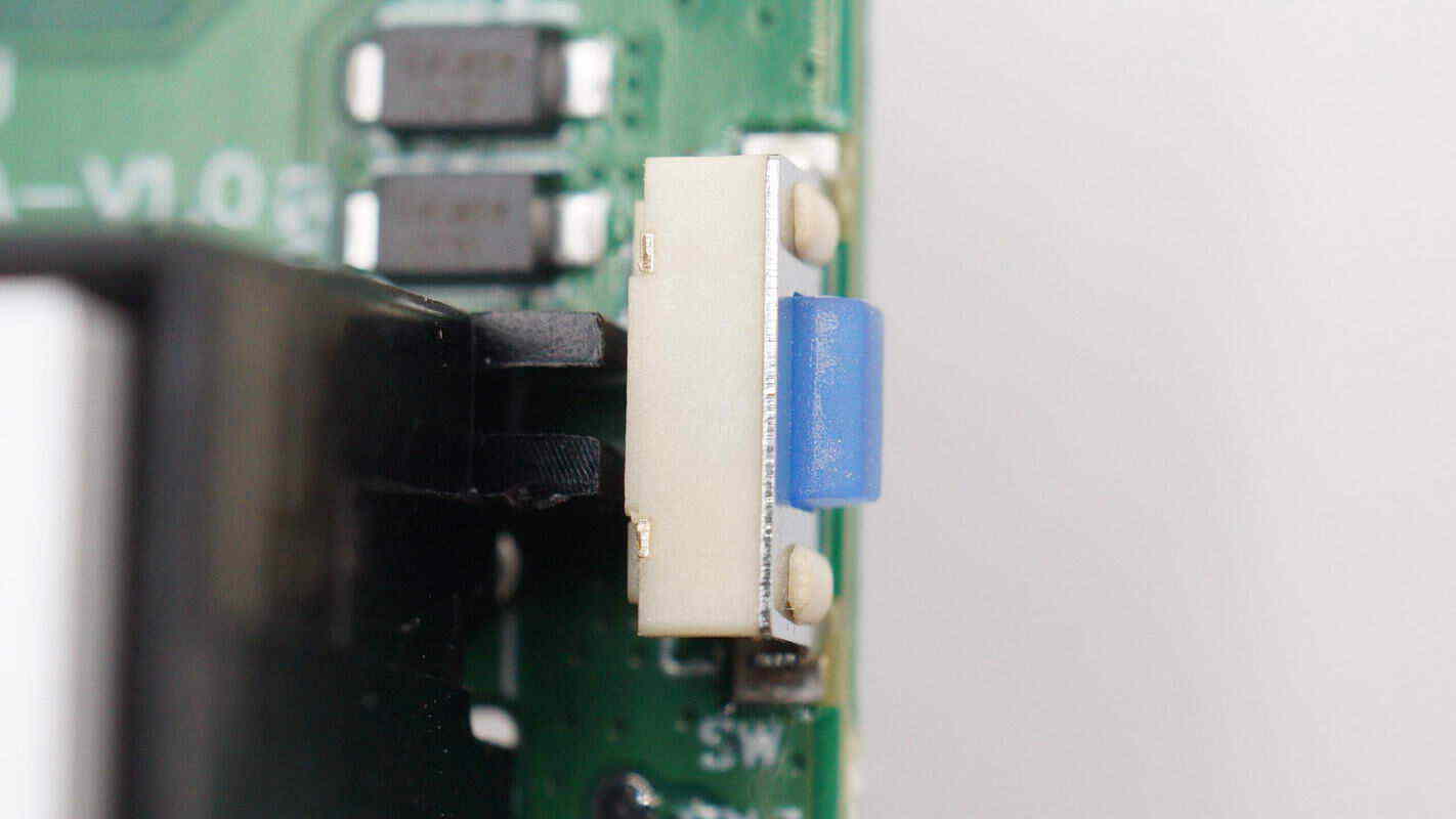
The power button is surface-mounted.
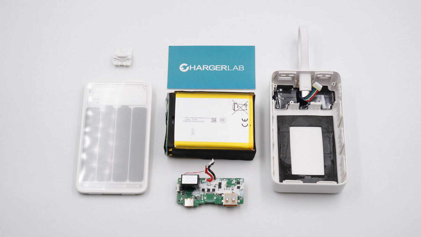
Well, those are all components of the realme 45W Cabled Power Bank.
Summary of ChargerLAB
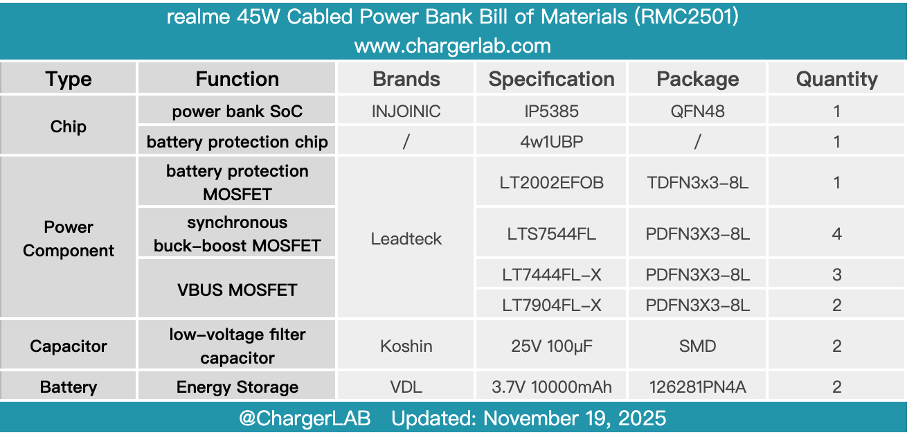
Here is the component list of the realme 45W Cabled Power Bank for your convenience.
It supports 45W output, features a built-in 20,000 mAh battery, and comes with a built-in USB-C braided cable, one USB-A port, and one USB-C port. It is compatible with multiple fast-charging protocols, including PD3.0, PPS, QC, and VOOC/SVOOC.
After taking it apart, we found that it contains two VDL soft-pack cells connected in series. The cell model is 126281PN4A, with a rated voltage of 3.7 V and a rated capacity of 10,000 mAh, and it has passed CCC certification. A battery protection chip works together with a battery protection MOSFET to manage and protect the battery pack. The pack is surrounded by abundant foam padding and insulated with Kapton tape. The pack is equipped with a thermistor and a battery protection PCB, reflecting high-quality internal components.
The master controller uses the Injoinic IP5385, a highly integrated power bank SoC, paired with four Leadteck LTS7544FL synchronous buck-boost MOSFETs. Leadteck LT7444FL‑X and LT7904FL‑X VBUS MOSFETs are used for port management, and the solid capacitors are from Koshin. The design demonstrates high integration and a well-organized PCB layout.
Related Articles:
1. Teardown of Belkin BoostCharge 45W GaN Wall Charger – Spider-Man Limited Edition (WCA013yz)
2. Teardown of Xiaomi 100W GaN Charger for Xiaomi 17 Series (MDY-18-EW)
3. Teardown of Belkin BoostCharge Pro 140W 4-Port GaN Wall Charger (WCH014)