Introduction
Today, we received an OPPO 120W SuperVOOC GaN Charger. It not only supports the SUPERVOOC fast-charging protocol but is also compatible with multiple fast-charging standards, including PD and PPS. Next, we will proceed with a teardown to examine its components and structure.
Product Appearance
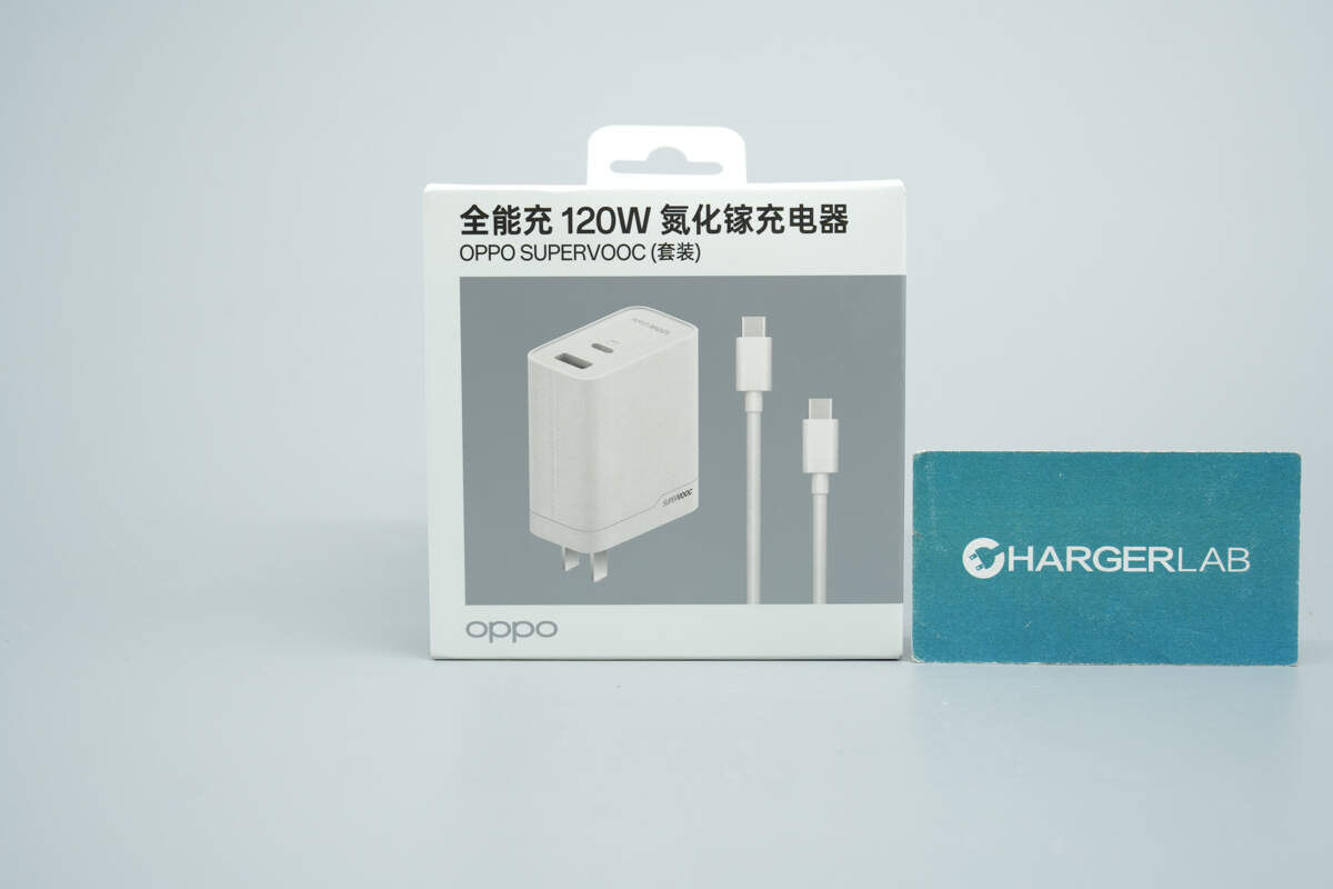
The front of the packaging features the OPPO logo, the product name, and an image of the kit.
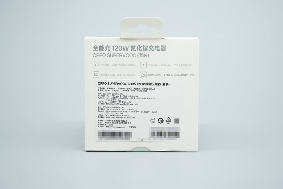
The back of the packaging displays the product name and key selling points, and also features a sticker with the specifications.
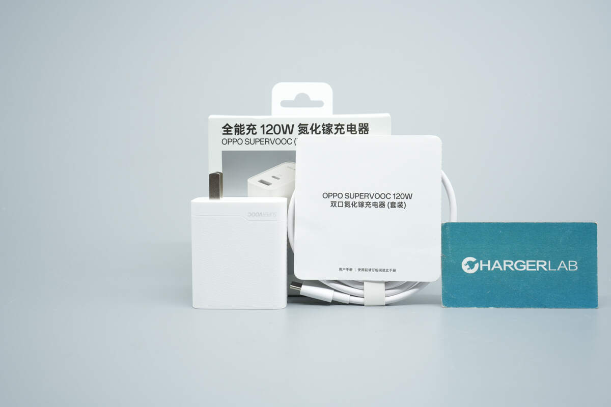
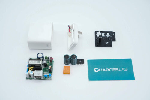
The package includes the charger kit and a user manual.
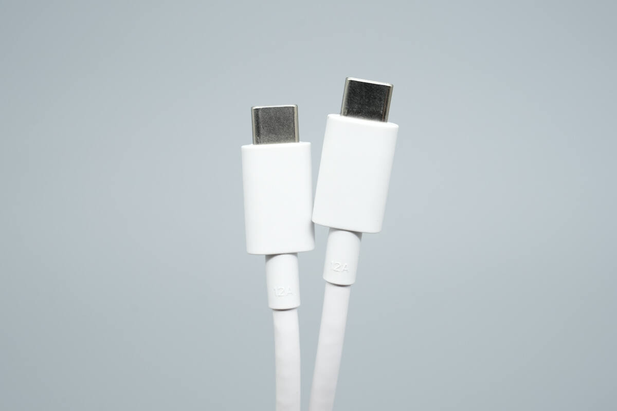
The included cable is a dual USB-C type.
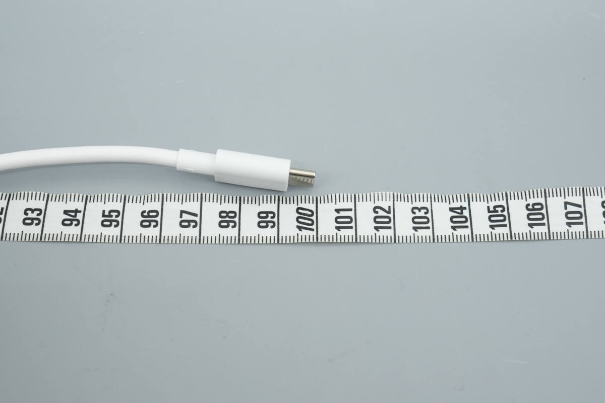
The length of the cable is about 100 cm (39.37 inches).
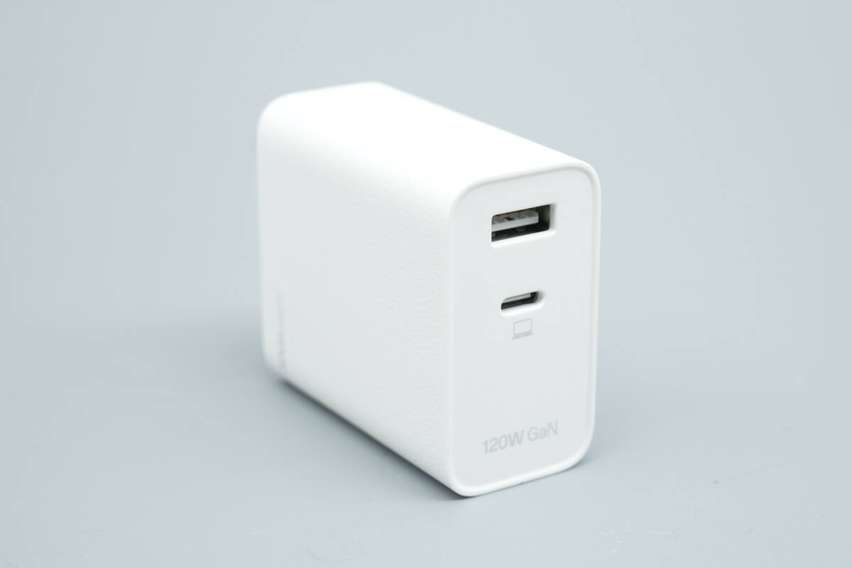
It features an all-white casing with a minimalist design.
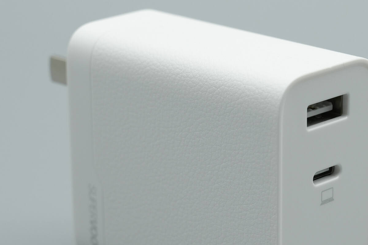
The sides are crafted with a laser-engraved technique to create a leather-like texture.
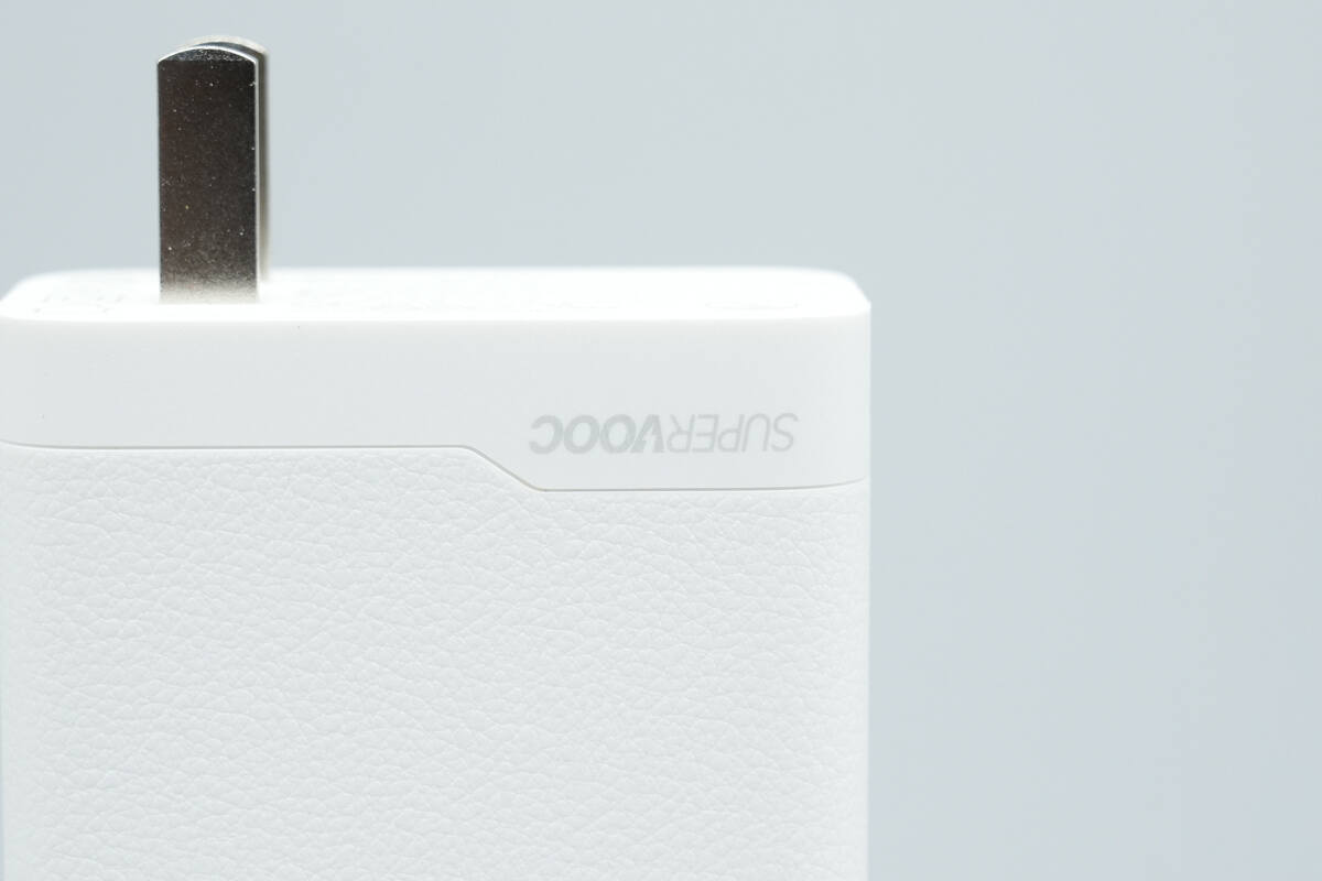
“SUPERVOOC” is printed here.
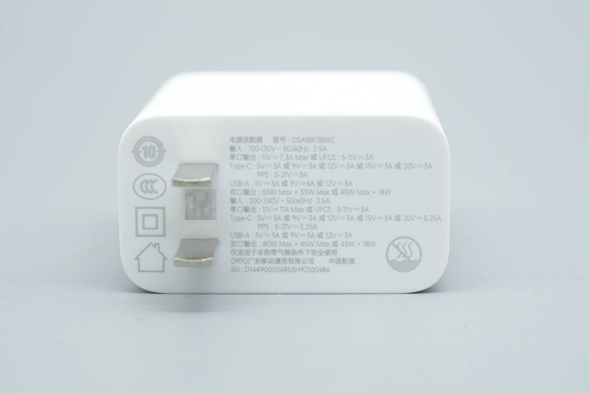
The input-side casing is printed with the specifications.
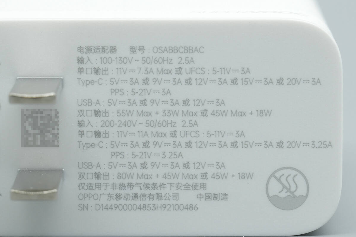
Model: OSABBCBBAC
Input: 100-130V~50/60Hz 2.5A
Single-port output: 11V 7.3A Max or UFCS: 5-11V = 3A
Type-C: 5V 3A, 9V 3A, 12V 3A, 15V 3A, 20V 3A
PPS: 5-21V 3A
USB-A: 5V 3A, 9V 3A, 12V 3A
Dual-port output: 55W Max + 33W Max or 45W Max + 18W
Input: 200-240V~50/60Hz 2.5A
Single-port output: 11V 11A Max or UFCS: 5-11V = 3A
Type-C: 5V 3A, 9V 3A, 12V 3A, 15V 3A, 20V 3.25A
PPS: 5-21V 3.25A
USB-A: 5V 3A, 9V 3A, 12V 3A
Dual-port output: 80W Max + 45W Max or 45W + 18W
The product has passed CCC certification.
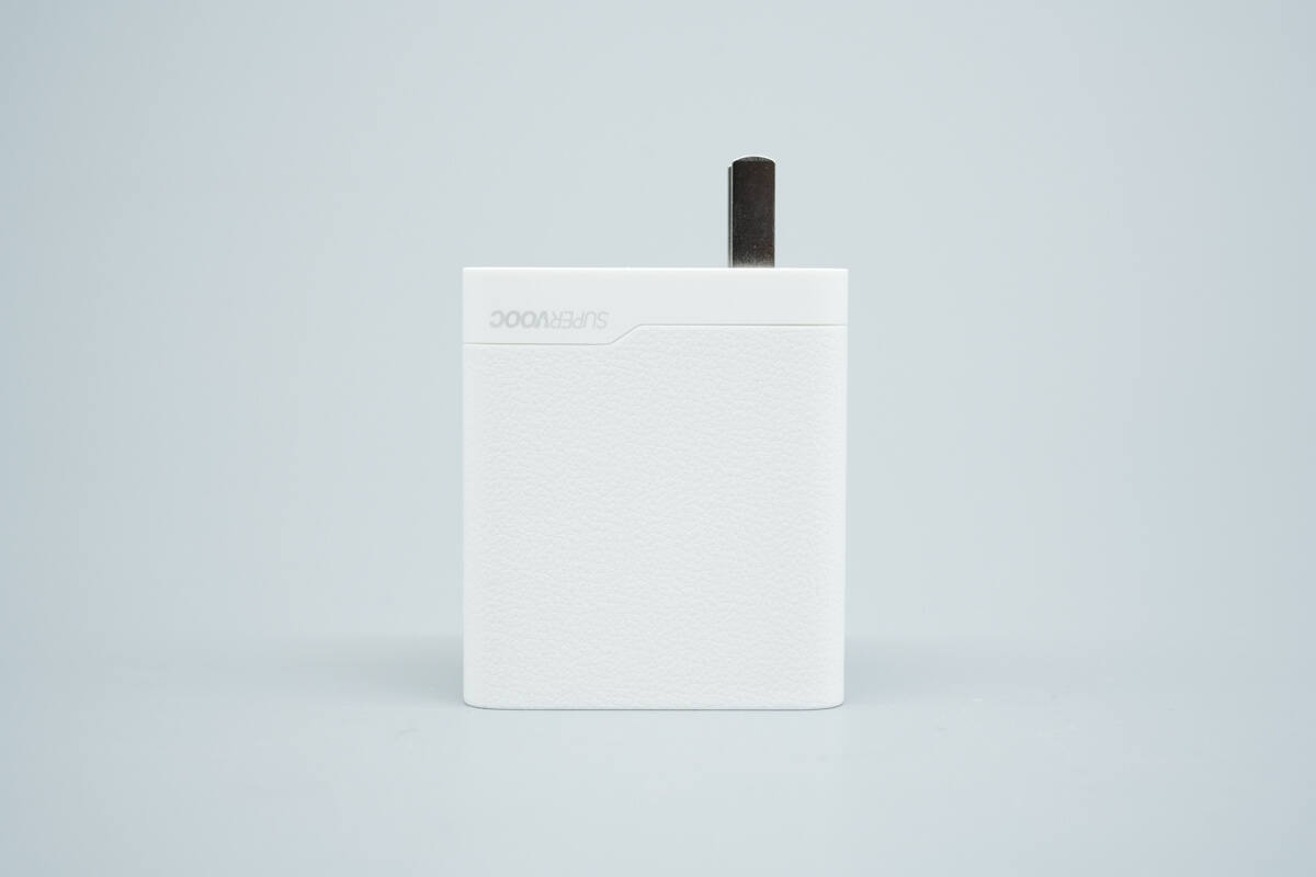
It comes with fixed prong pins.
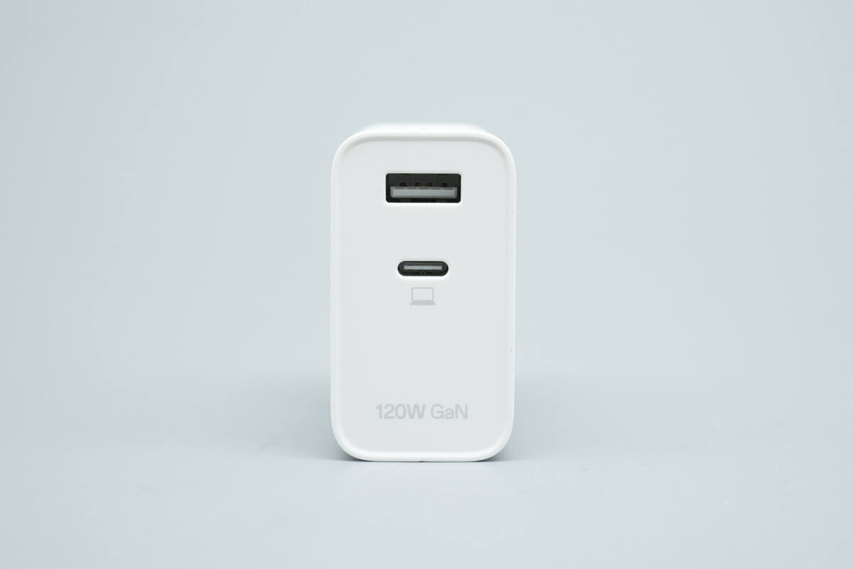
The top features one USB-A port and one USB-C port.
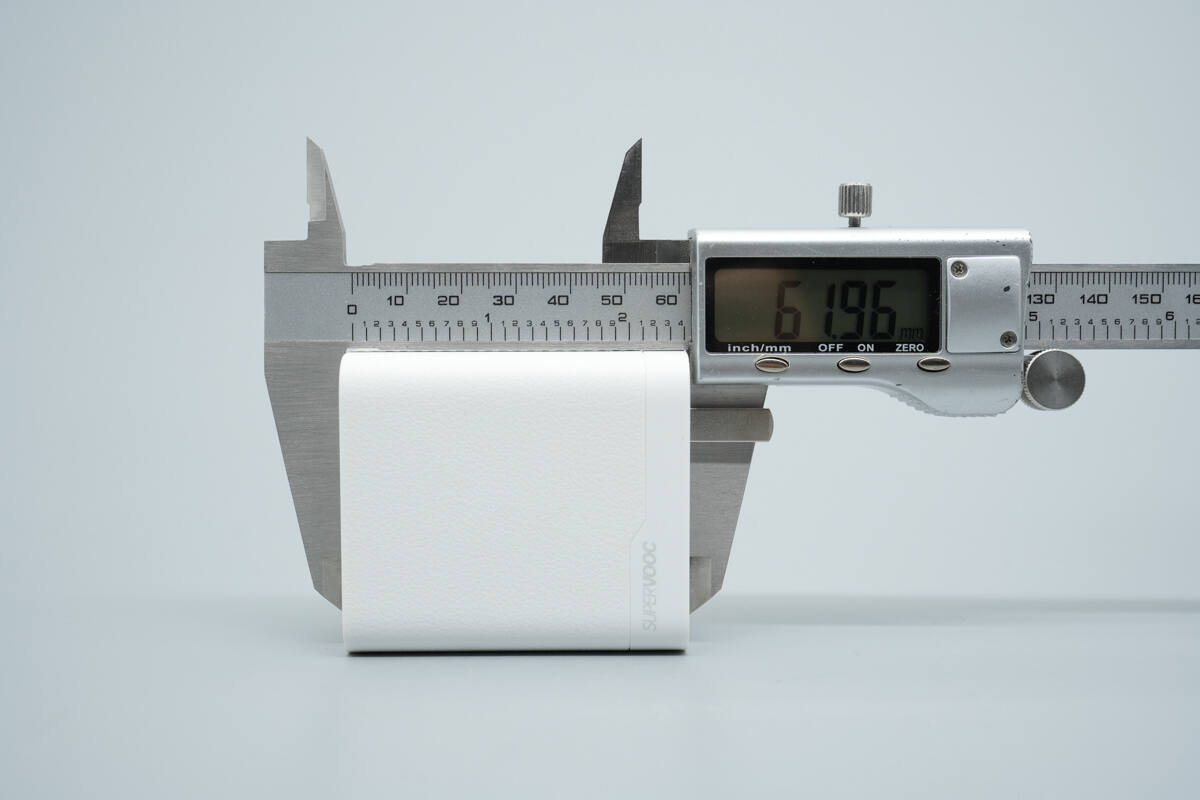
The length of the charger is about 61.96 mm (2.44 inches).
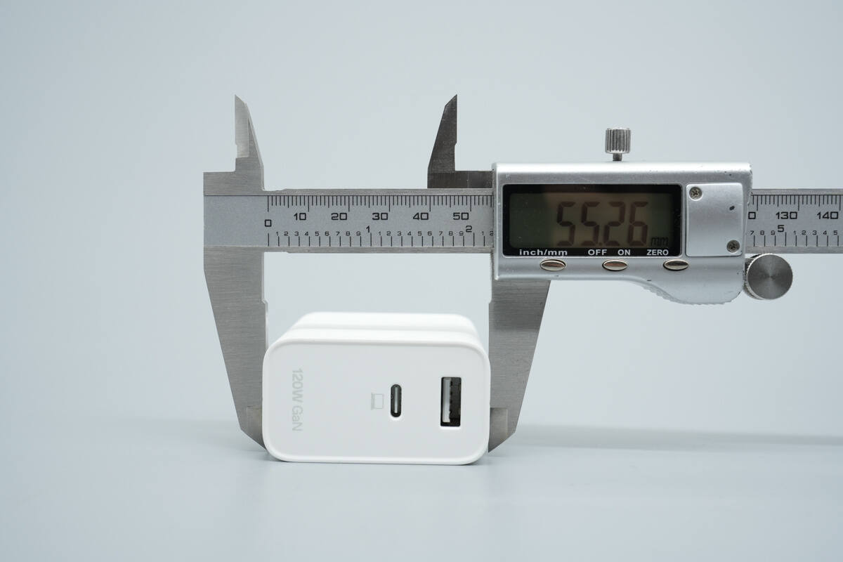
The width is about 55.26 mm (2.18 inches).
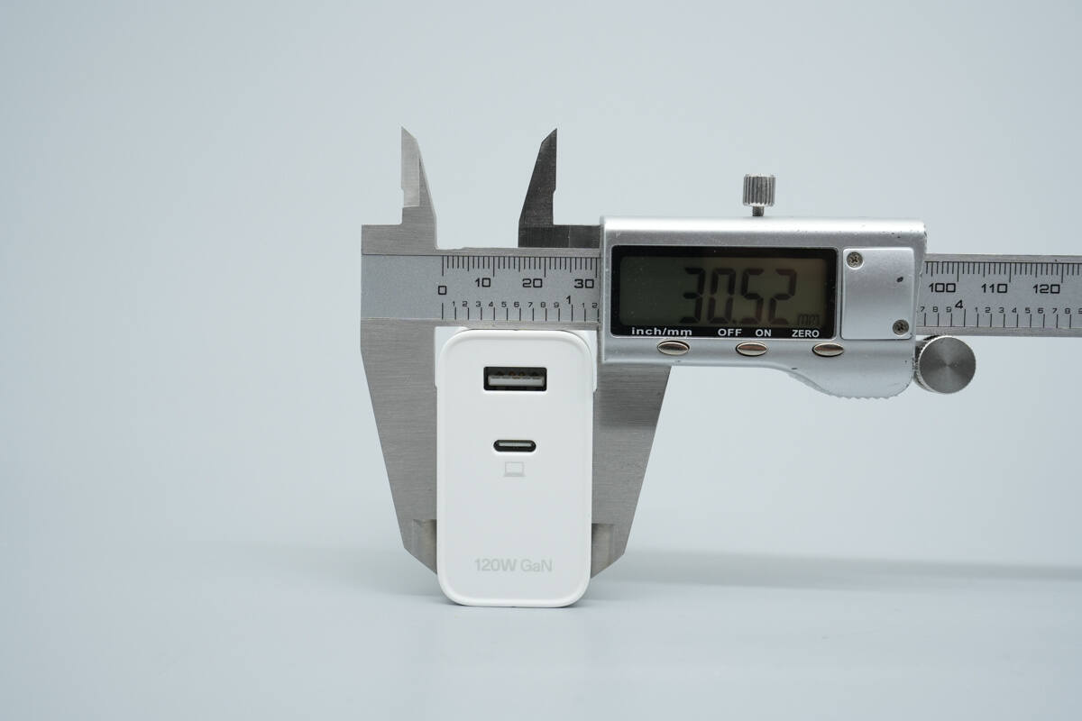
The thickness is about 30.52 mm (1.2 inches).
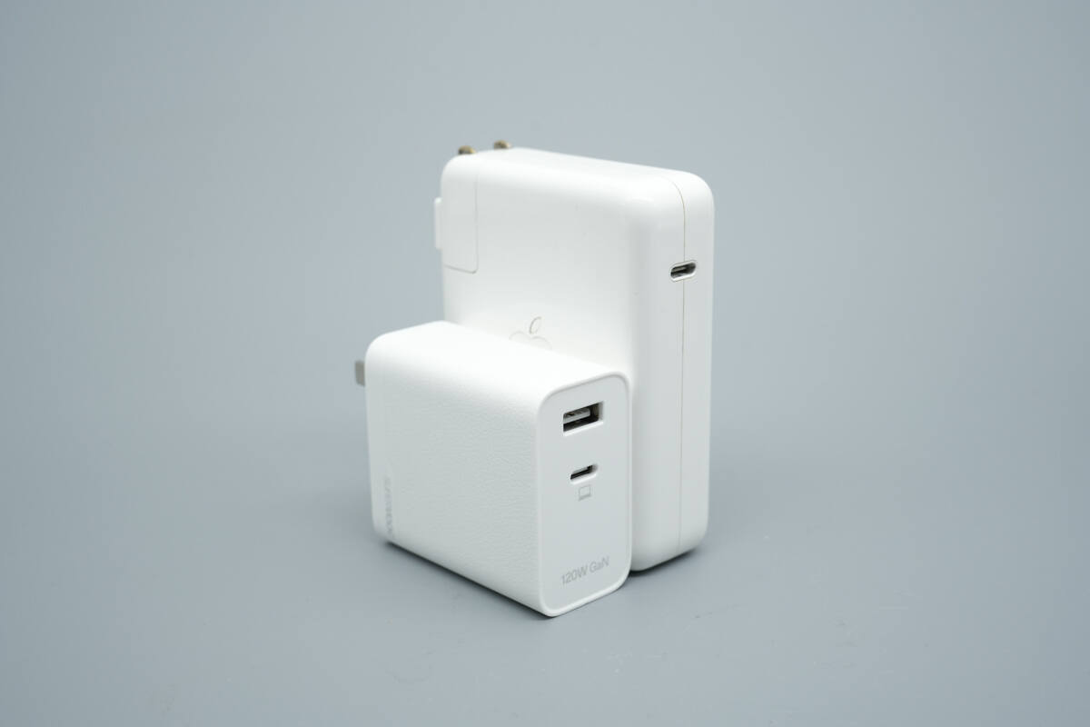
Compared side by side with the Apple 140W charger, it is significantly smaller in size.

That's how big it is in the hand.
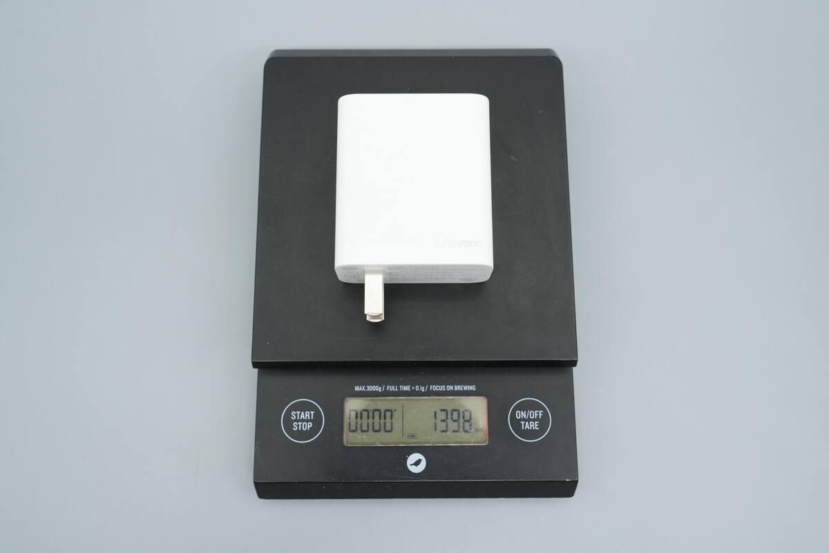
The weight is about 140 g (4.94 oz).
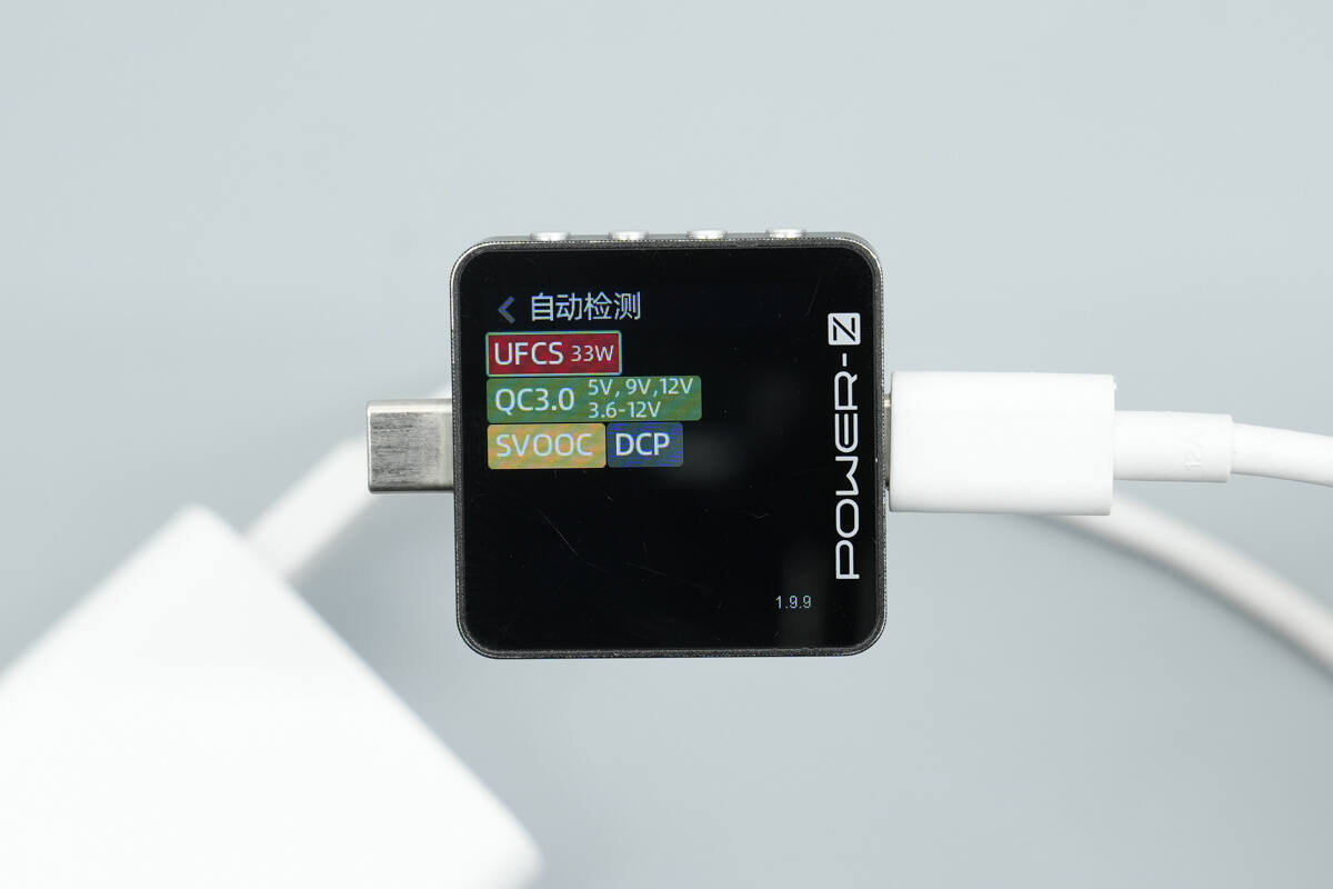
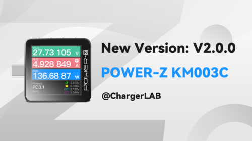
ChargerLAB POWER-Z KM003C shows that the USB-A port supports UFCS, QC3.0, SVOOC, and DCP charging protocols.
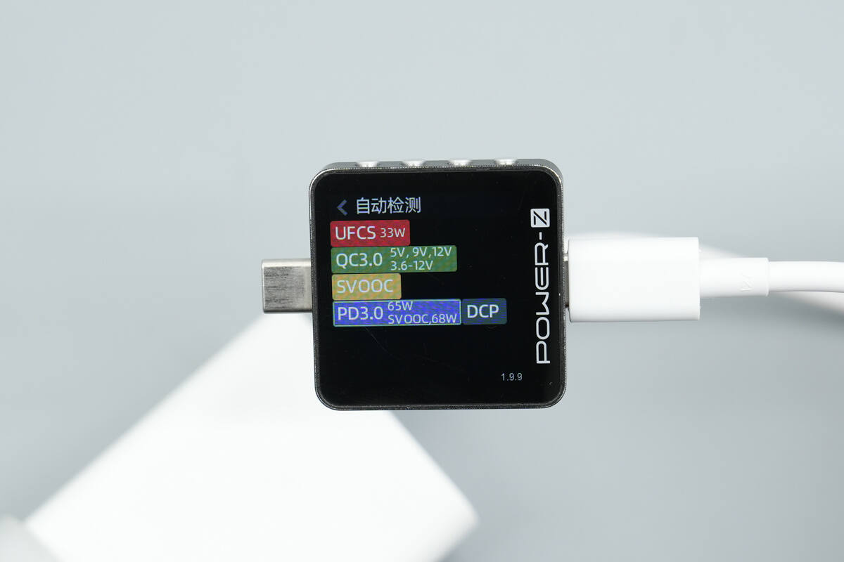
The USB-C port supports UFCS, QC3.0, SVOOC, PD3.0, and DCP charging protocols.
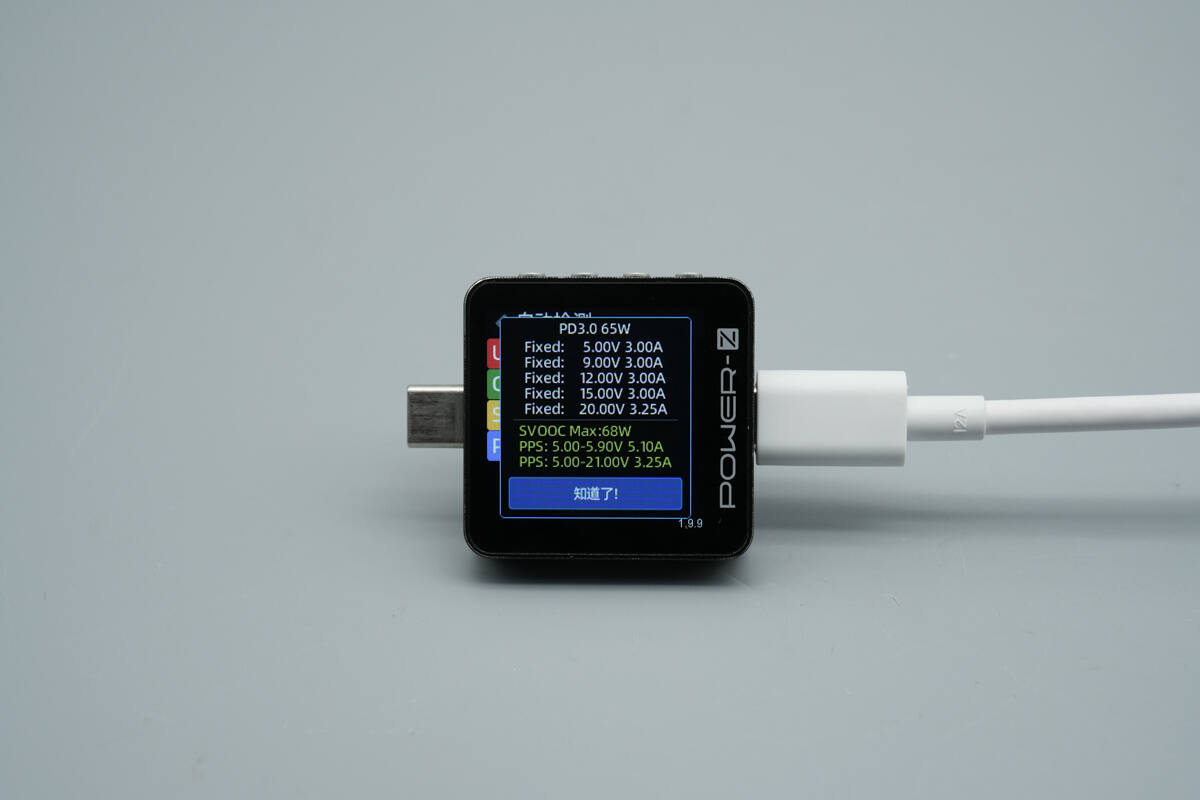
It features five fixed PDOs: 5V3A, 9V3A, 12V3A, 15V3A, 20V3.25A, as well as two PPS voltage ranges: 5-5.9V 5.1A and 5-21V 3.25A.
Teardown
Next, let's take it apart to see its internal components and structure.
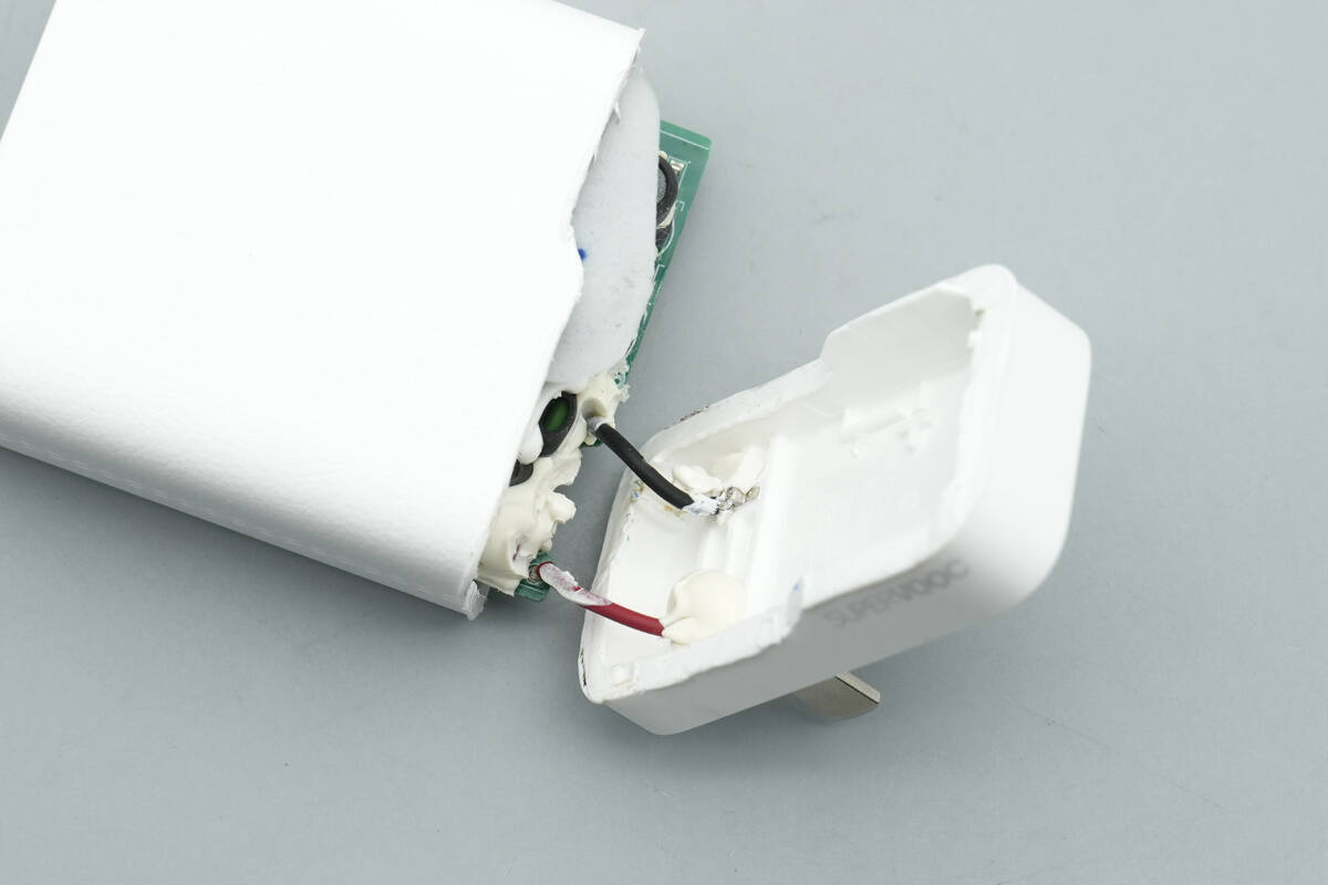
Open the input-side casing, revealing that the prongs are connected via wires.
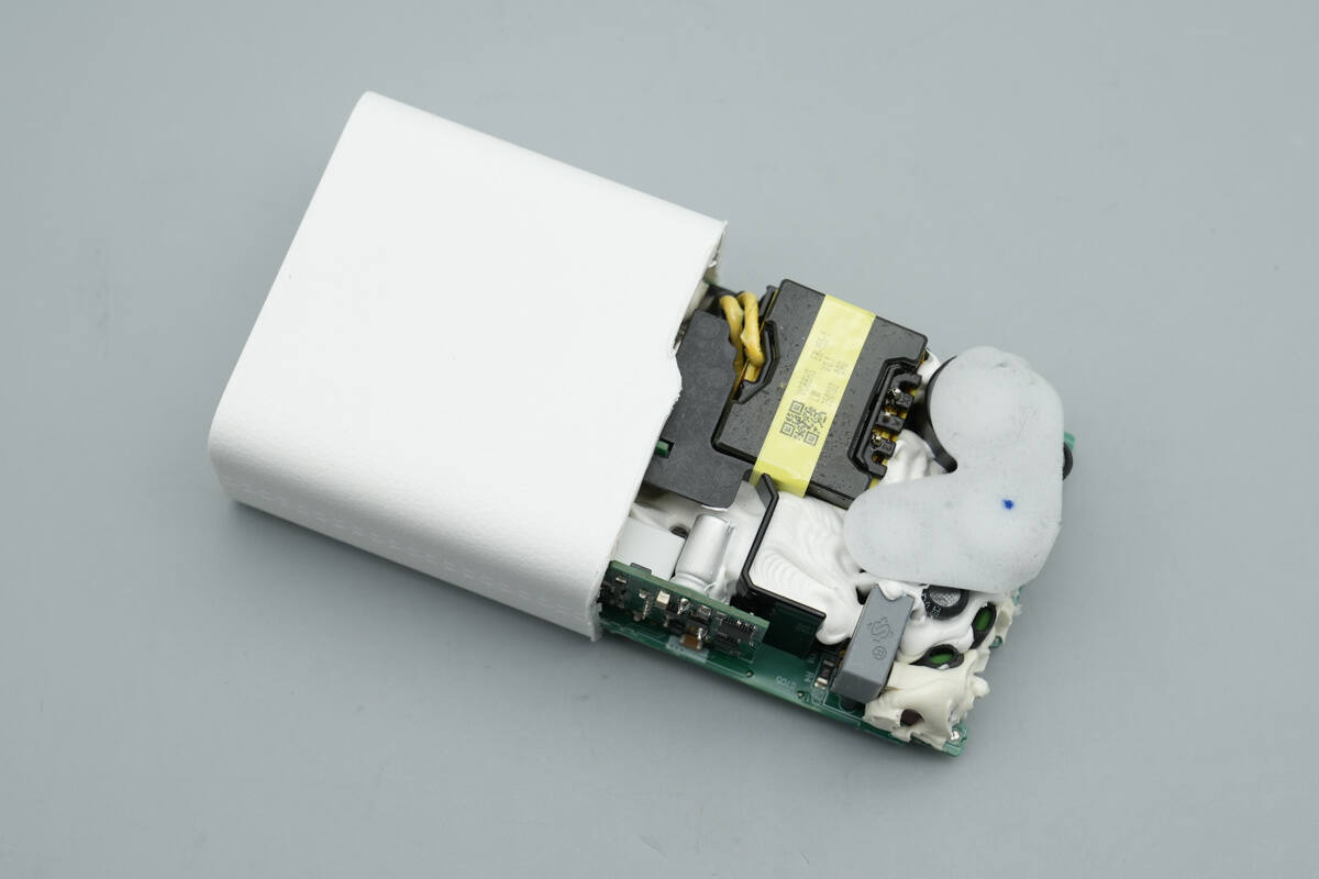
Remove the PCBA module.
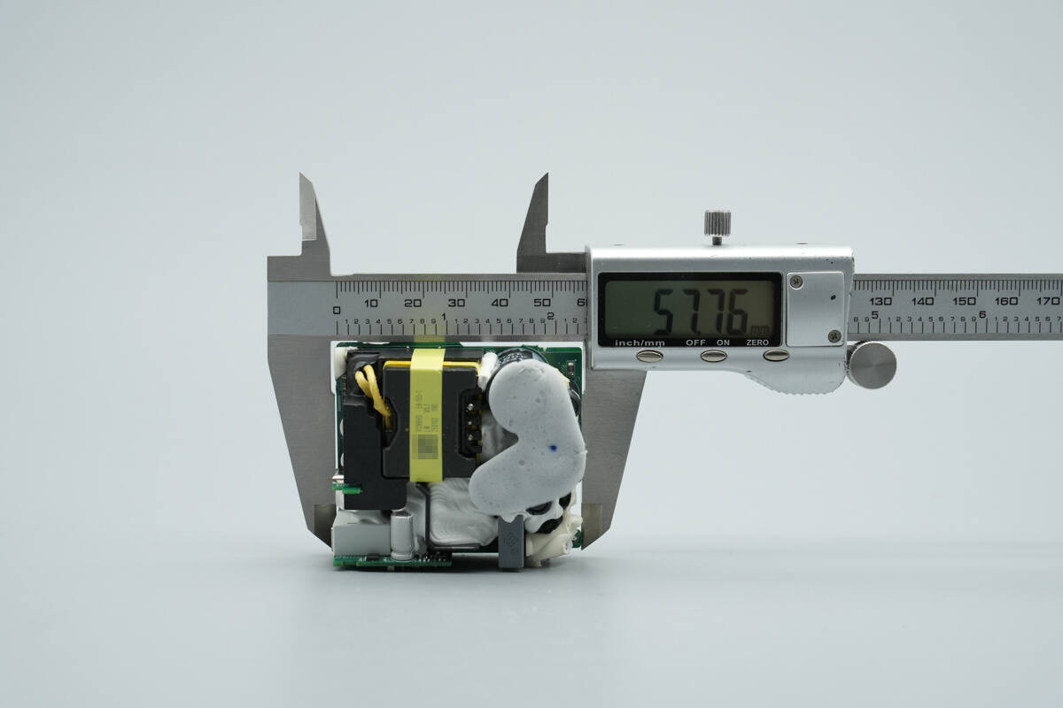
The length of the PCBA module is about 57.76 mm (2.27 inches).
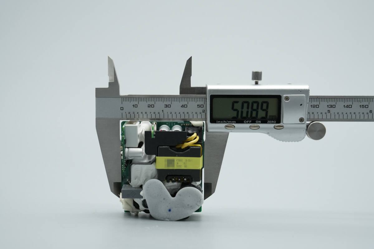
The width is about 50.89 mm (2.0035 inches).
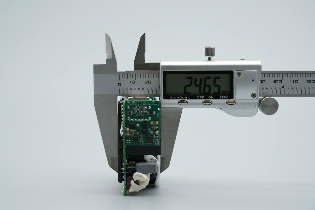
The thickness is about 24.65 mm (0.97 inches).
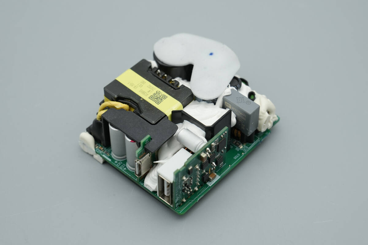
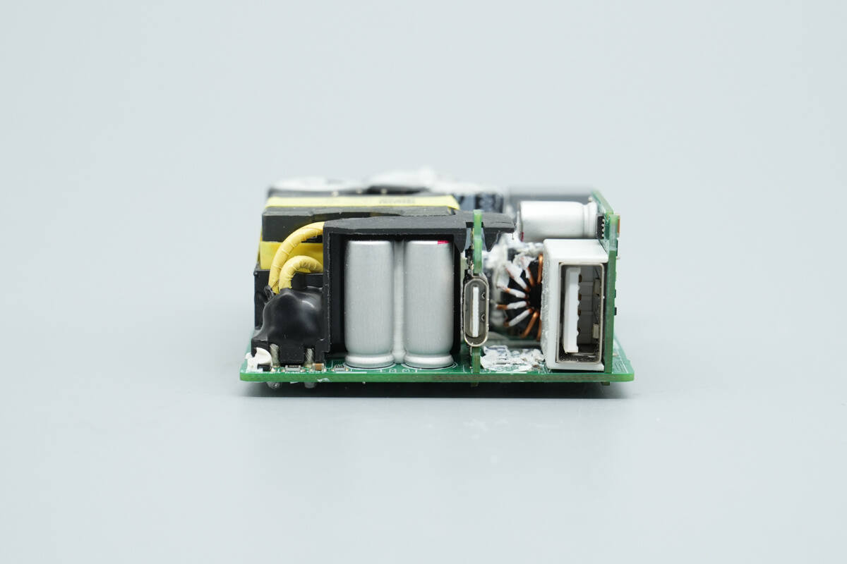
The components on the front of the PCBA module are reinforced with adhesive, and the area around the transformer features isolation and insulation treatment.
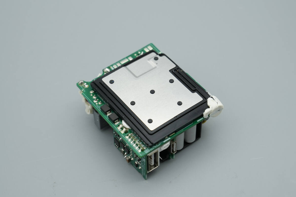
The bottom of the module is covered by a plastic isolation plate and a heatsink.
The front of the PCBA module houses components such as a fuse, filter capacitors, a bridge rectifier, and a transformer.
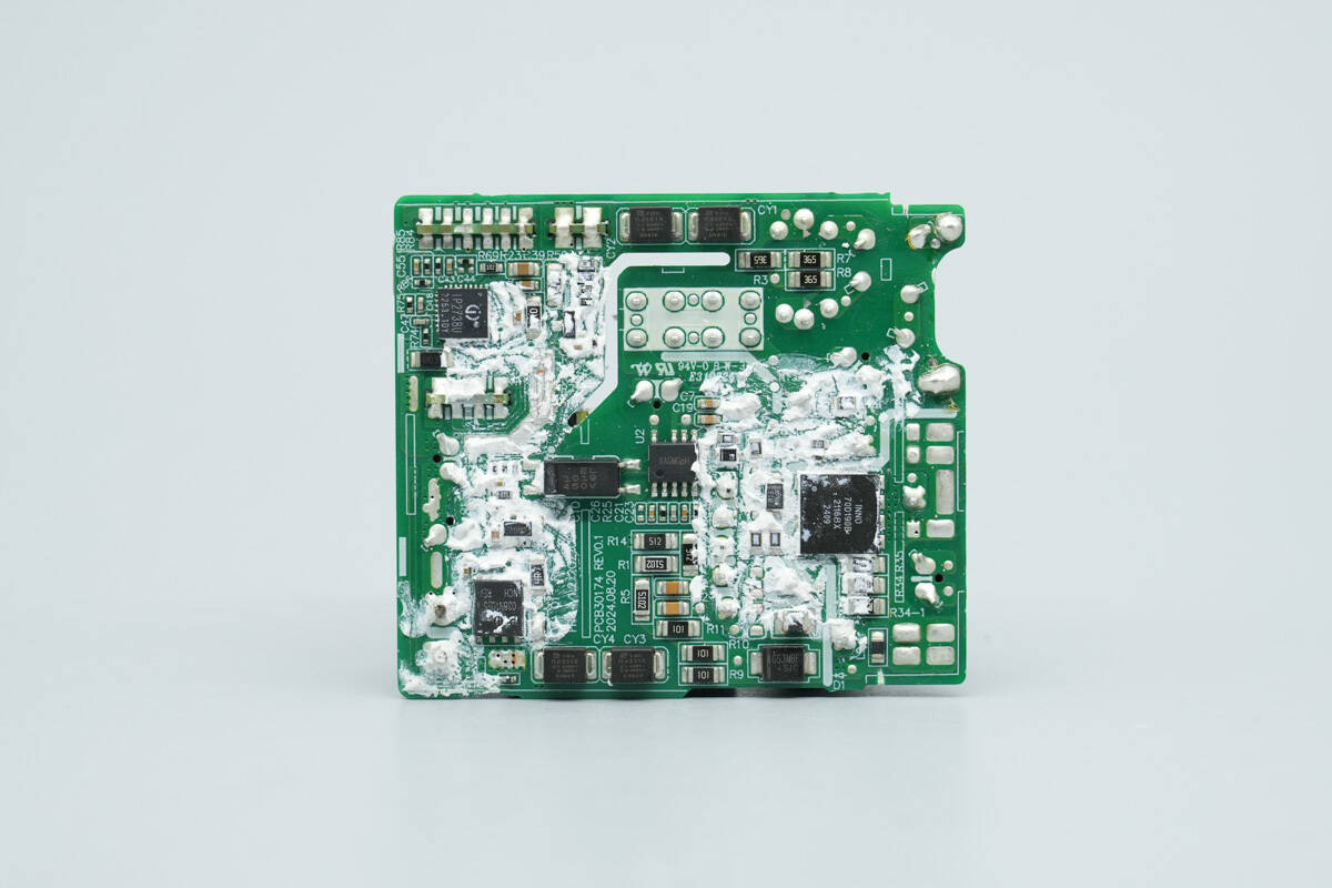
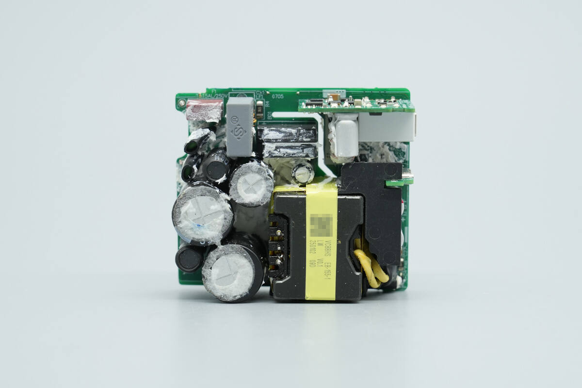
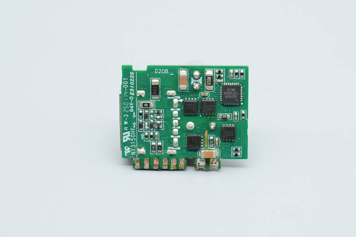
The back of the module contains the master control chip, primary MOSFET, synchronous rectifier, and protocol chip.
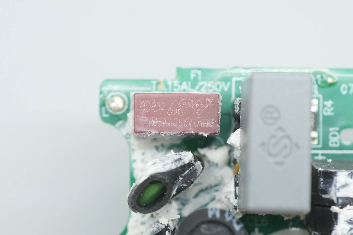
The delay fuse is from Betterfuse, part number 932, rated at 3.15A 250V.
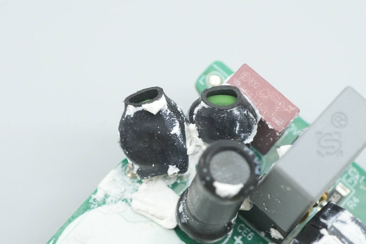
The NTC thermistors are used to suppress inrush current at power-up, and both are insulated with heat-shrink tubing.
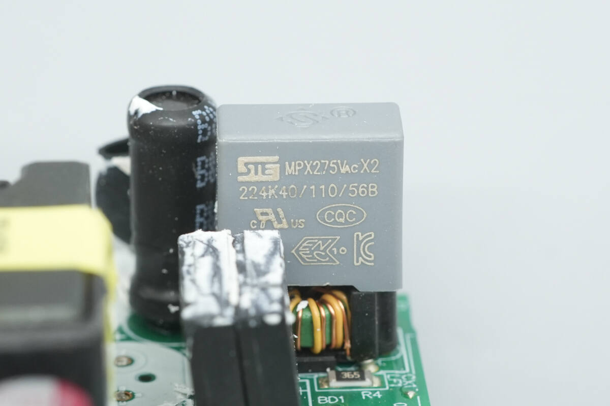
The safety X2 capacitor is from STE, with a capacitance of 0.22 μF.
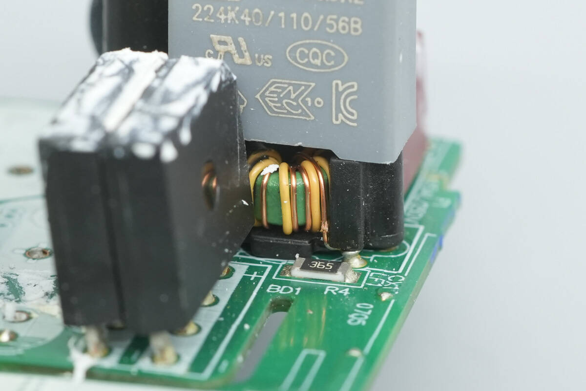
The safety X2 capacitor is supported by plastic posts on its leads, and a common-mode choke is positioned below to filter EMI interference.
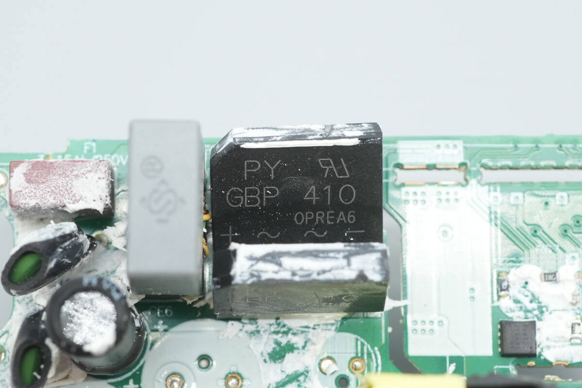
The bridge rectifier is from PY, model GBP410, rated at 4A 1000V, and comes in a GBP package.
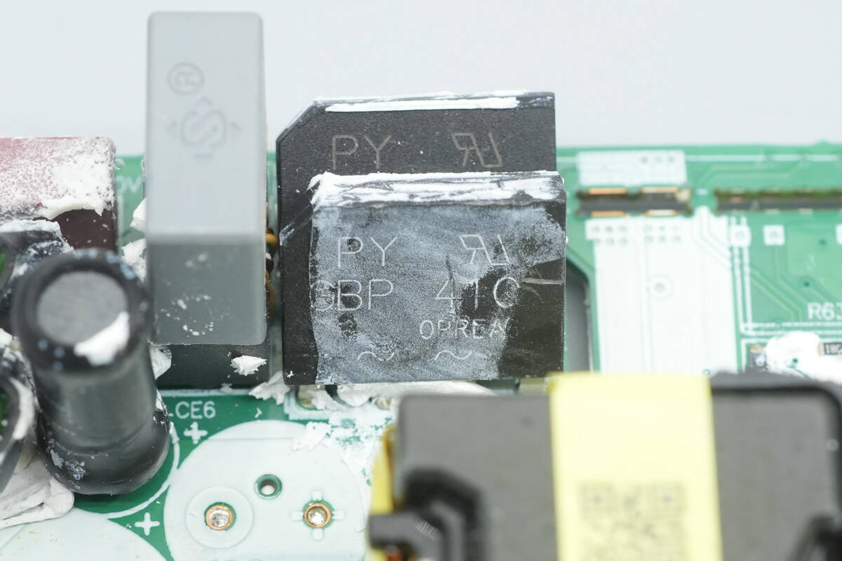
The other bridge rectifier is identical to the first one.
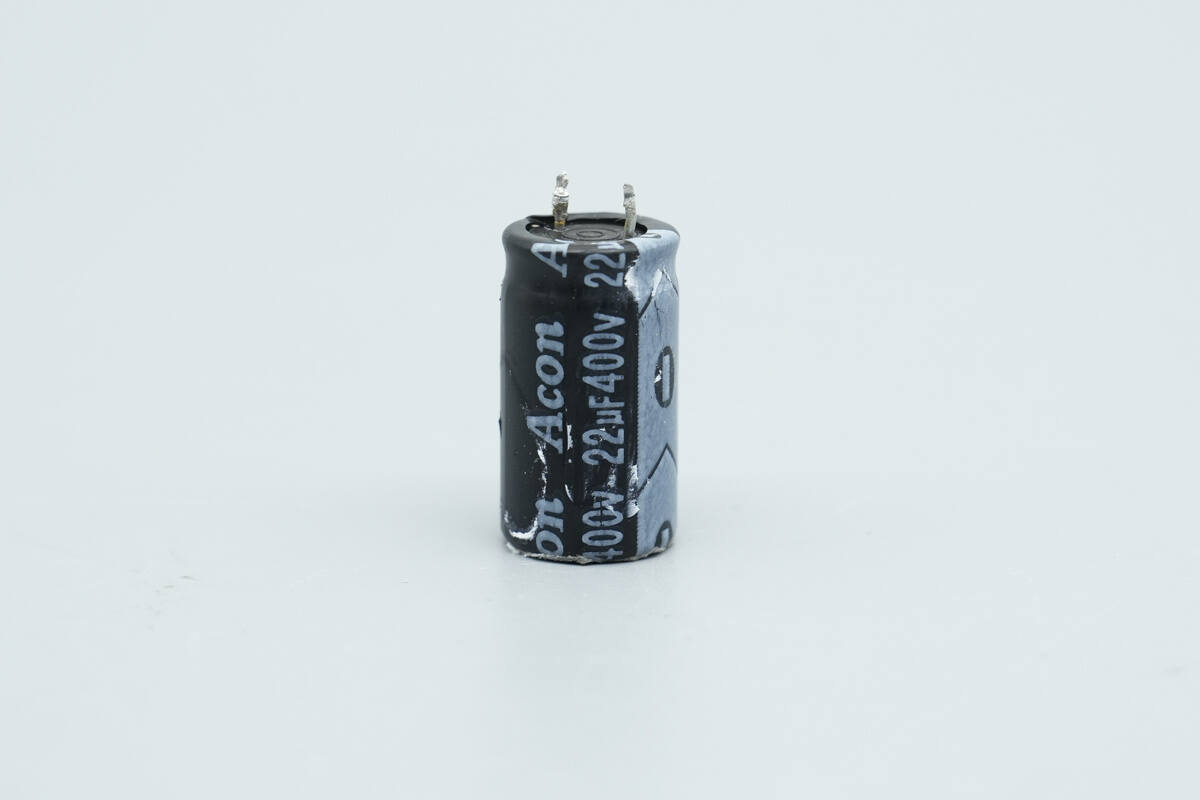
The high-voltage filter electrolytic capacitor is from Acon, rated at 400V 22 μF.
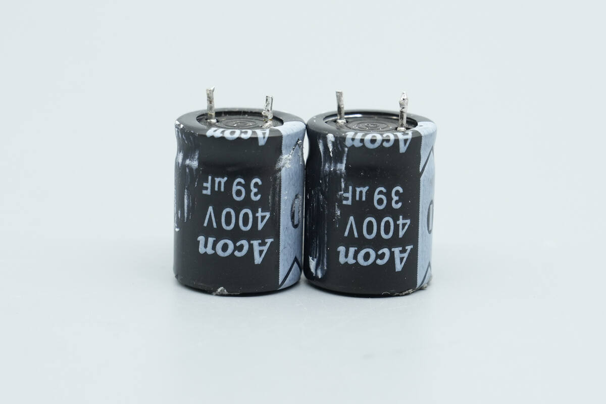
The other two are also from Acon, each rated at 400V 39 μF.
The I-shaped inductor is insulated with heat-shrink tubing.
A close-up of the other I-shaped inductor.
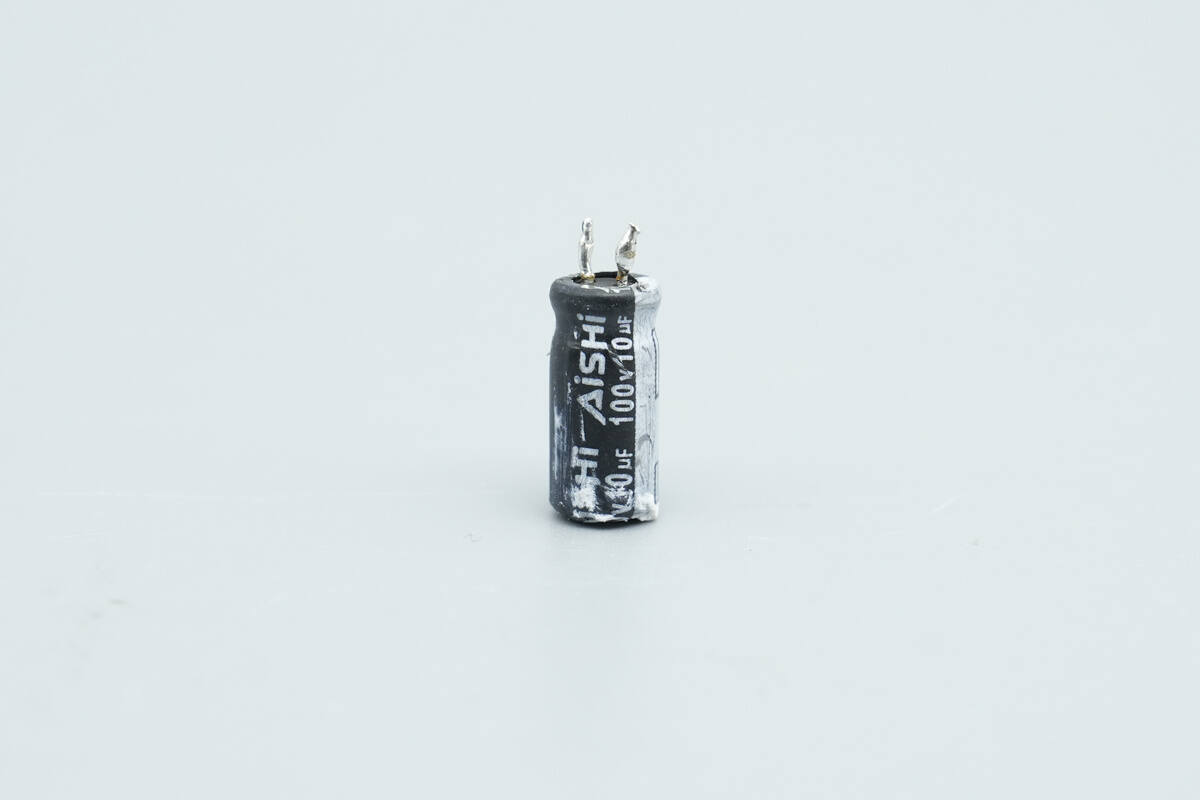
The capacitor supplying power to the master control chip is from AiSHi, rated at 100V 10 μF.
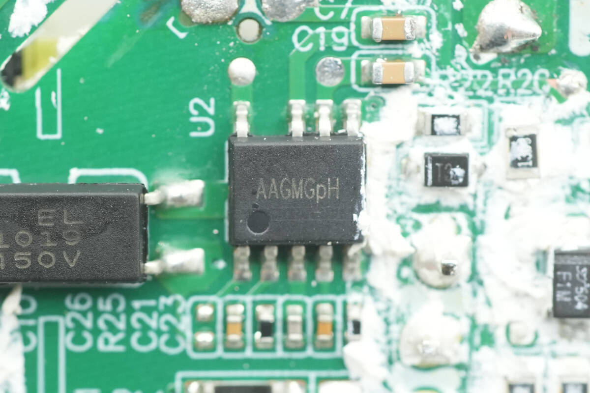
The primary master control chip is from Silergy, marked with AAGM, and comes in an SSOP-9 package.
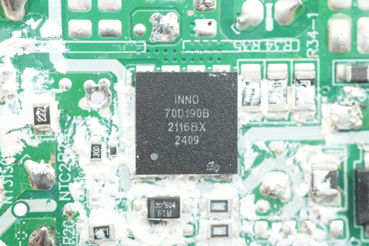
The primary MOSFET is from Innoscience, model INN700DA190B. It is a 700V enhancement-mode GaN transistor, upgraded from the previous 650V rating, with a transient voltage tolerance of 800V. The device has an on-resistance of 190 mΩ, supporting higher-power applications.
It supports ultra-high switching frequencies, has no reverse-recovery charge, and features extremely low gate and output charges. It meets JEDEC standards for industrial applications, includes built-in ESD protection, and complies with RoHS, lead-free, and EU REACH regulations. It is suitable for high-efficiency, high-density applications such as AC-DC and DC-DC conversion. The MOSFET comes in a DFN 5×6 package.
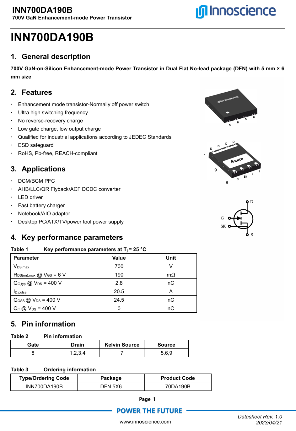
Here is the information about Innoscience INN700DA190B.
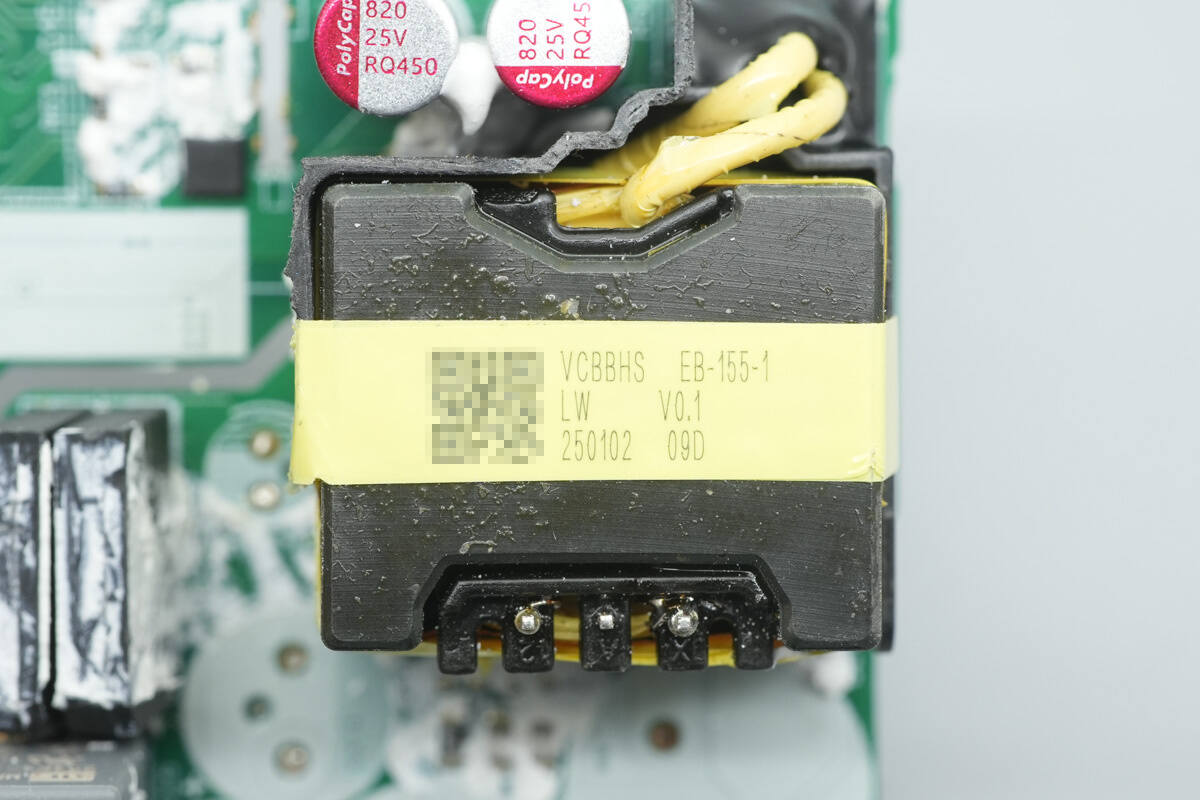
A close-up of the transformer.
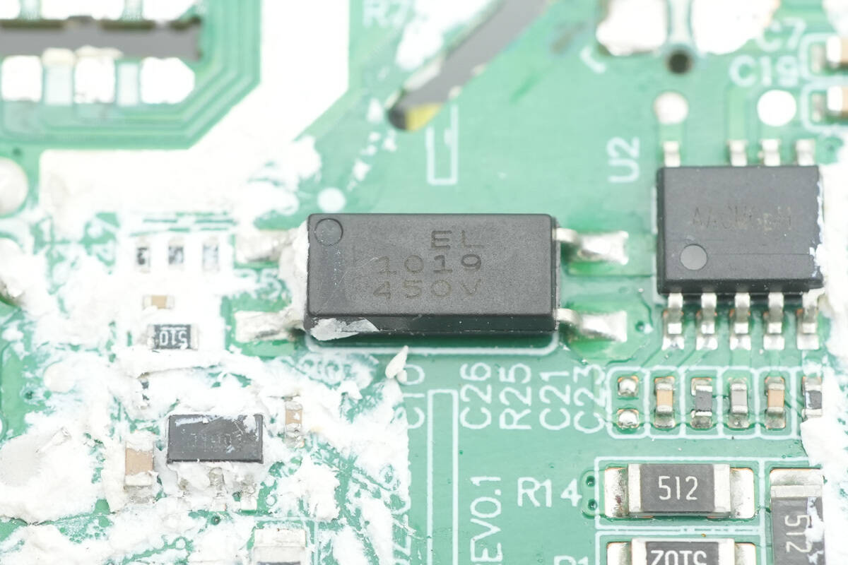
The Everlight EL1019 optocoupler is used for output voltage feedback.
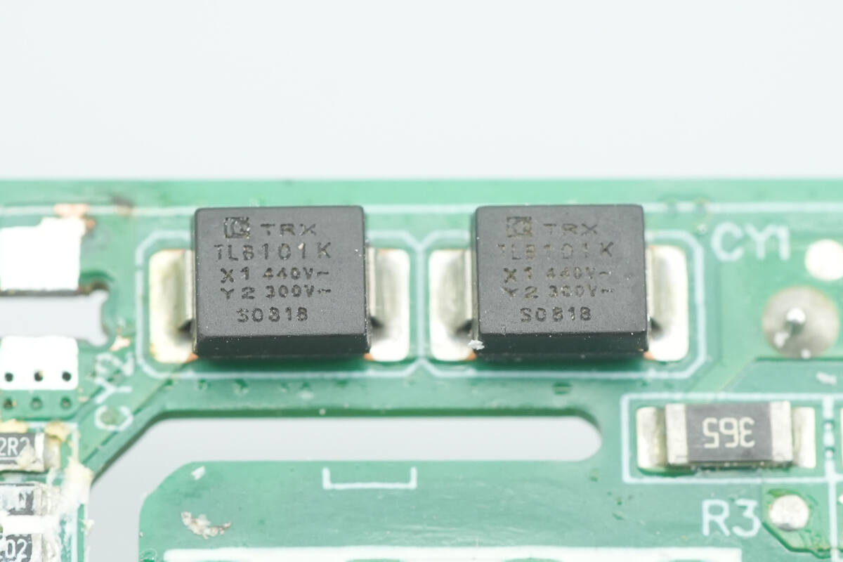
The SMD Y capacitors are from TRX, part number TBY2101KB. Their compact size and light weight make them well-suited for high-density power products, such as GaN fast chargers.
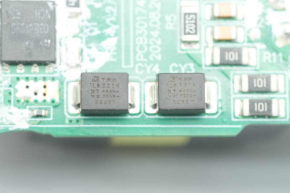
The other two TRX SMD Y capacitors are part number TBY2331KB.
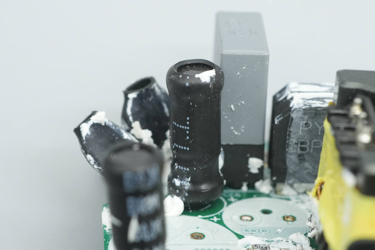
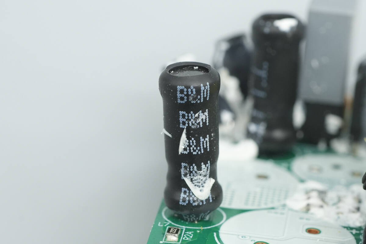
The solid capacitors are reinforced with adhesive, and the sockets for both interfaces are soldered onto separate small PCBs.
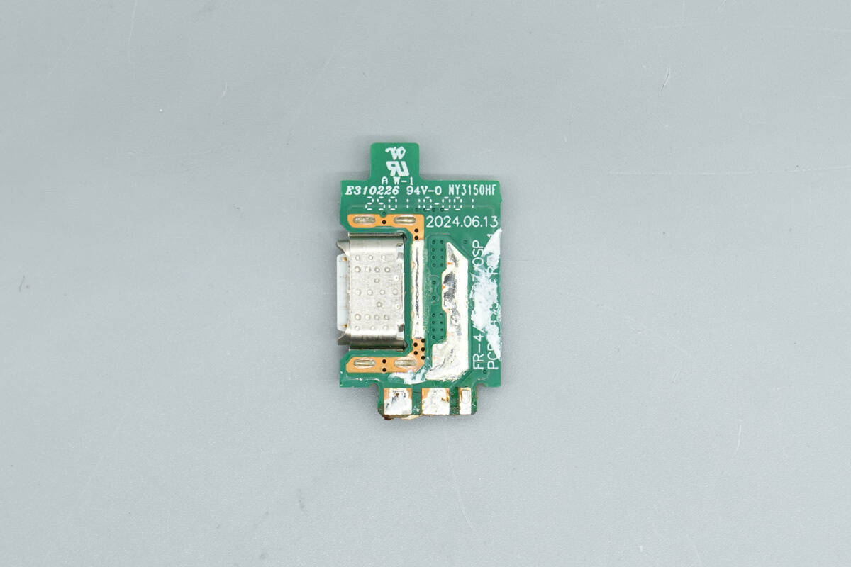
Remove the small PCB hosting the USB-C socket.
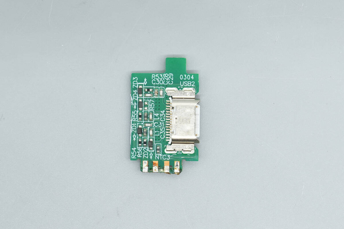
A view of the other side of the small PCB.
The USB-A socket is reinforced with a plastic housing. On the front of the small PCB, there is a buck-boost MOSFET, a VBUS MOSFET, a buck-boost inductor, and a solid capacitor.
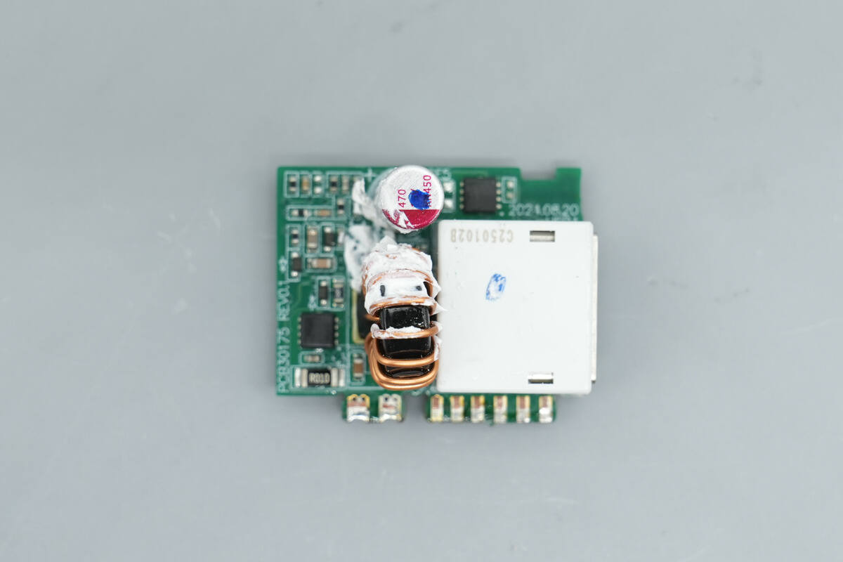
The other side features a synchronous buck-boost controller, a synchronous buck-boost MOSFET, and VBUS MOSFETs.
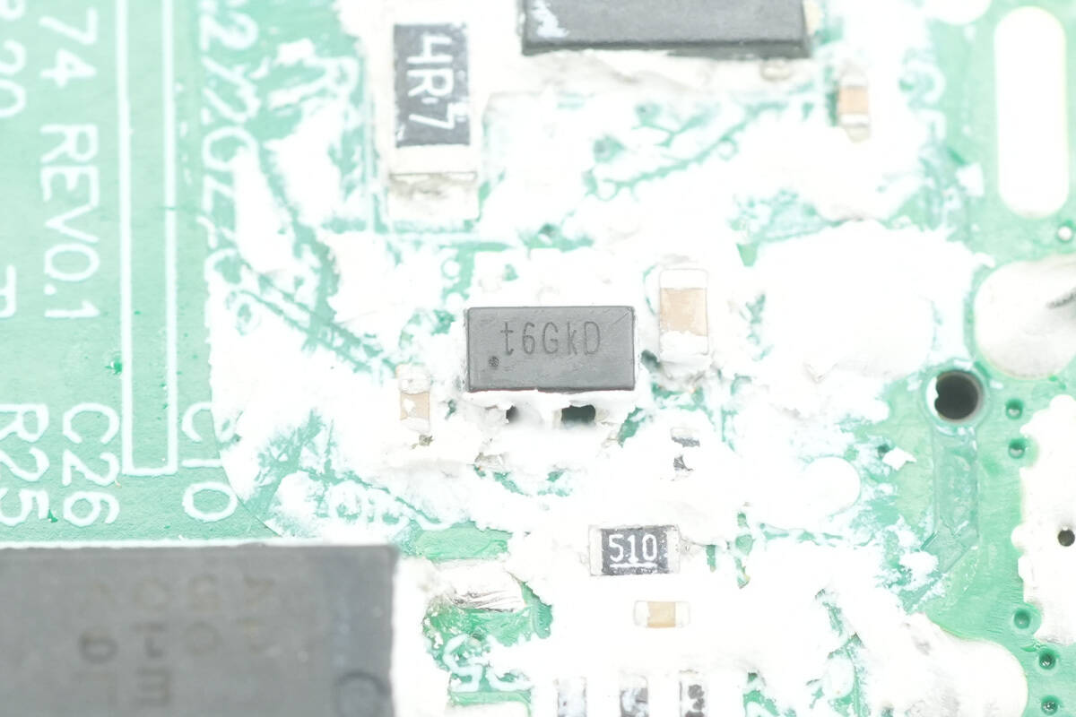
The synchronous rectifier controller is from Silergy, marked with t6.
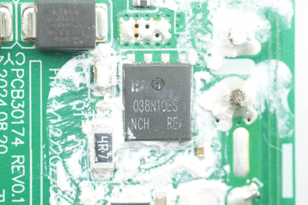
The synchronous rectifier is from PY, model PW038N10ESL. It is an NMOS with a voltage rating of 100 V and an on-resistance of 3.2 mΩ, housed in a DFN 5×6 package.
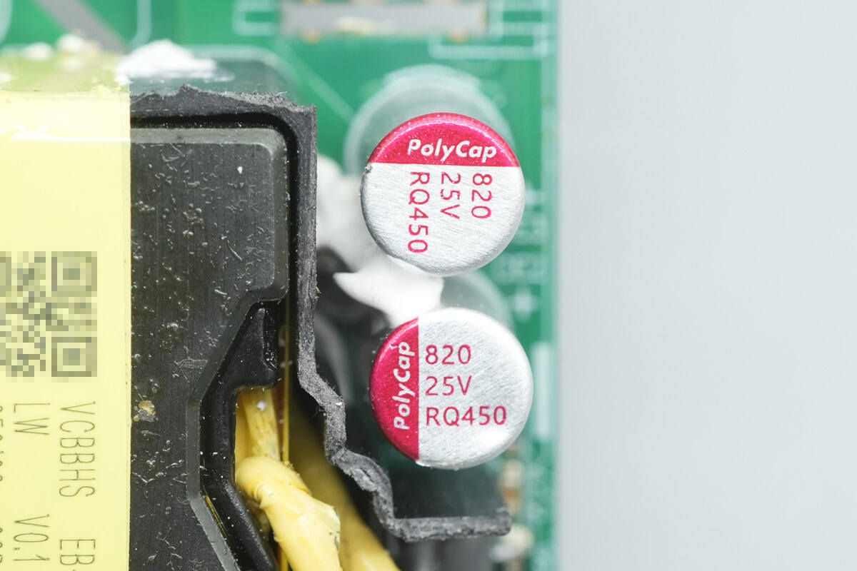
The two solid capacitors are from PolyCap, each rated at 25 V 820 μF.
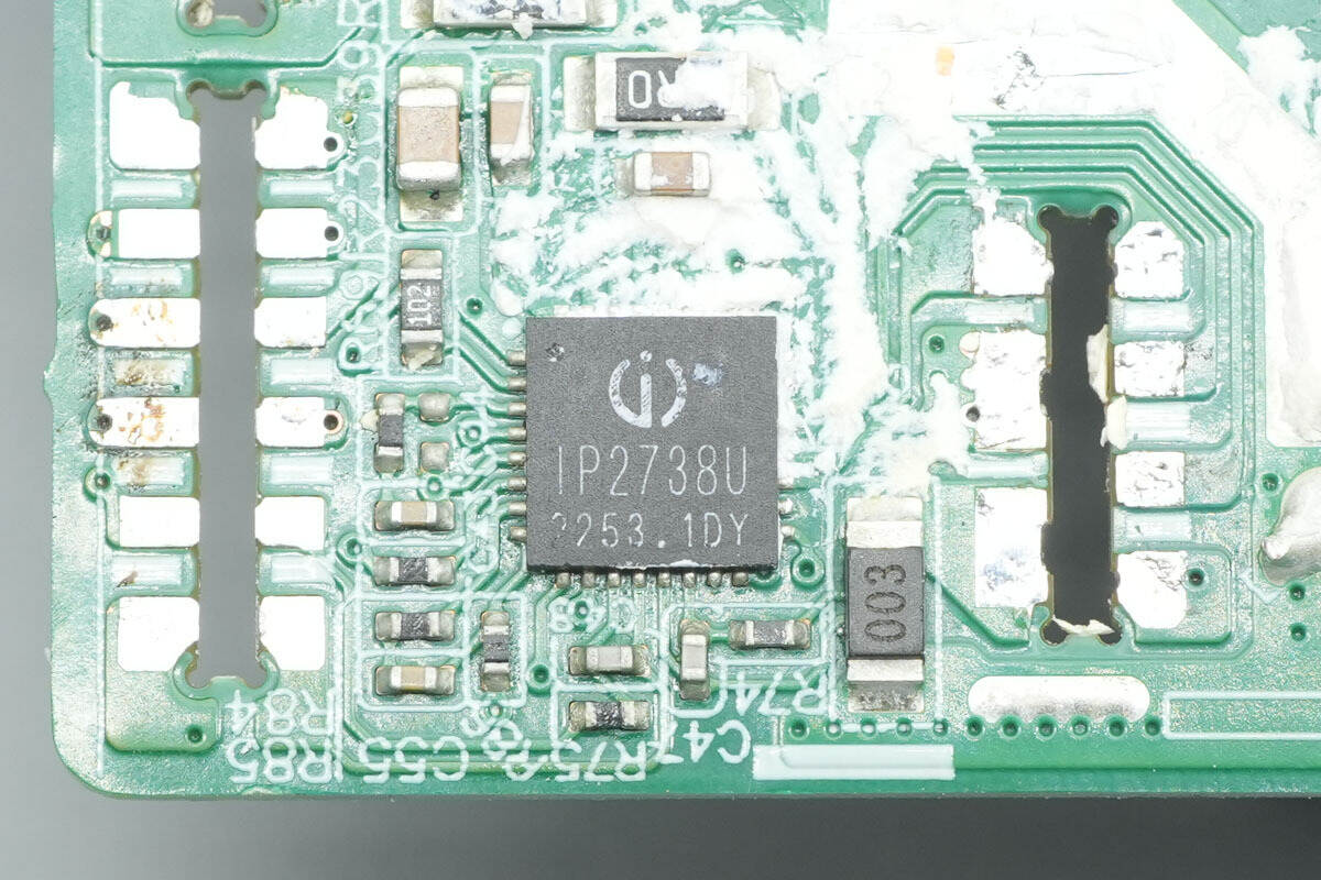
The protocol chip is from Injoinic, model IP2738U. It is a multi-USB interface protocol chip that supports dual-port 18–140 W fast-charging applications. It features independent feedback control and separate USB PD management, effectively integrating the functionality of two IP2736 chips into a single device, with fast-charging specifications equivalent to the IP2736. It supports USB PD 3.1 28 V EPR levels, UFCS fusion fast charging, as well as USB PD 3.0, PPS, and a wide range of other fast-charging protocols, offering excellent compatibility.
The Injoinic IP2738U includes four independent NMOS drivers for controlling multiple output ports, managing multiple VBUS MOSFETs for port switching, and enabling dual power-path parallel control. It also provides independent dual-channel overcurrent, overvoltage, and short-circuit protection, ensuring safe operation.
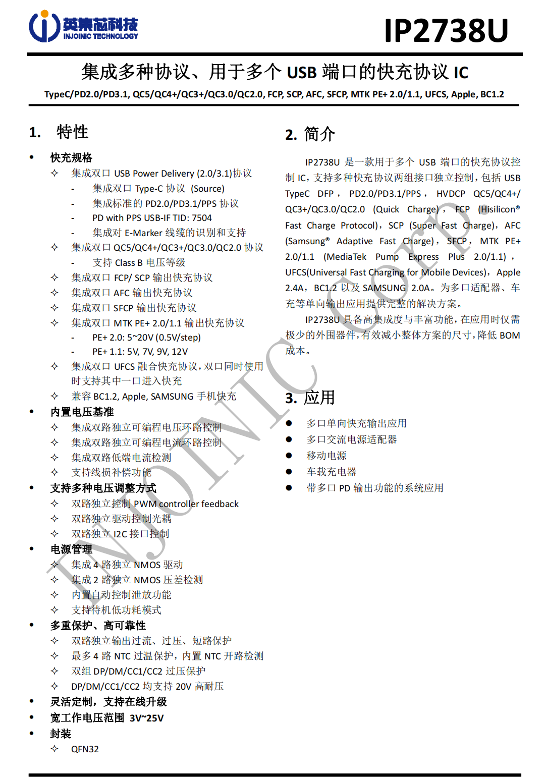
Here is the information about Injoinic IP2738U.
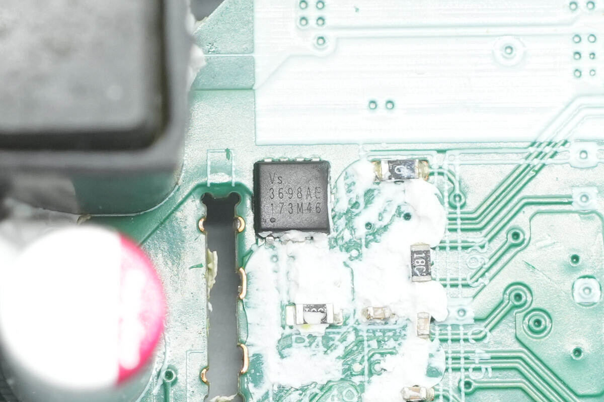
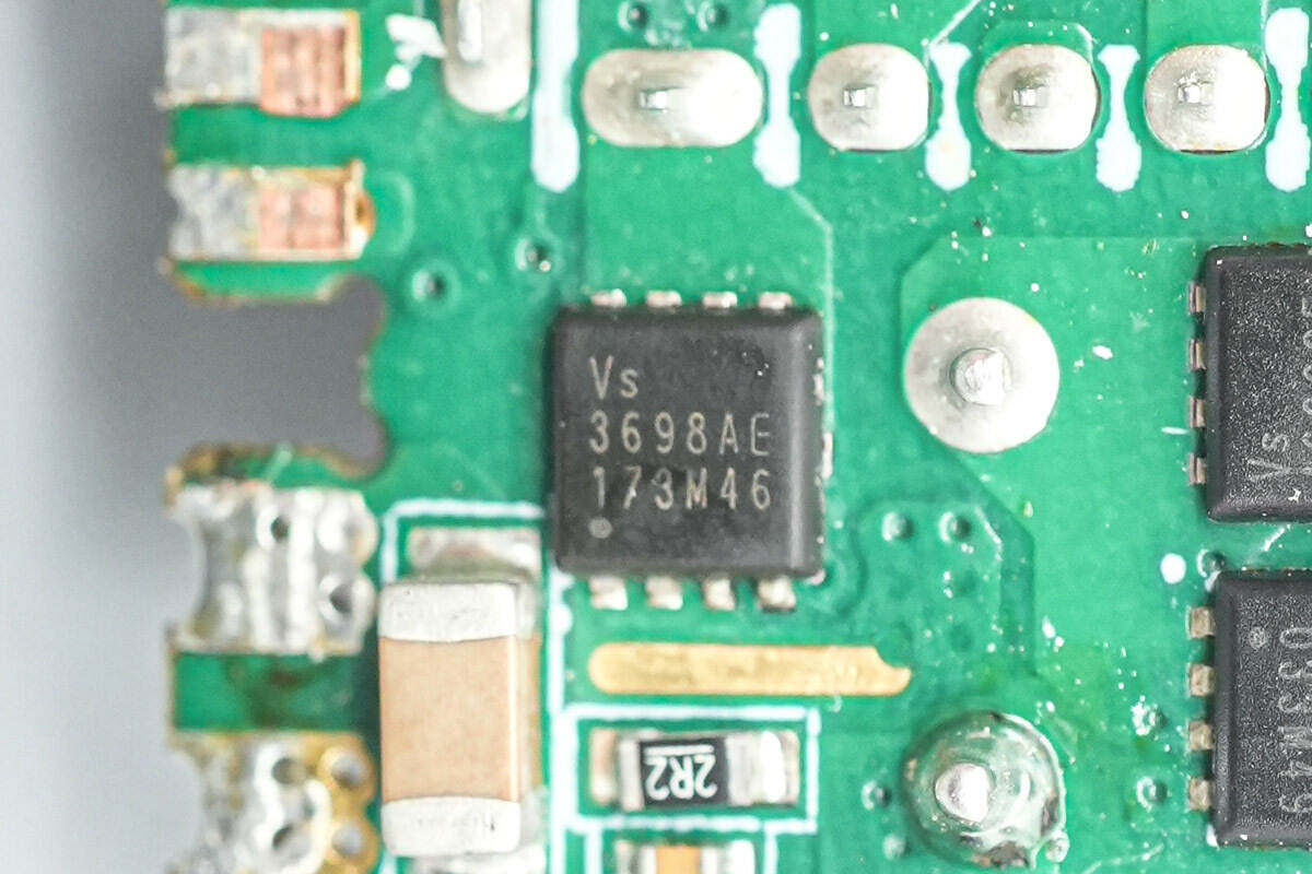
The output VBUS MOSFET is from Vergiga, model VS3698AE. It is an NMOS with a voltage rating of 30 V and an on-resistance of 3 mΩ, housed in a PDFN 3×3×3 package.
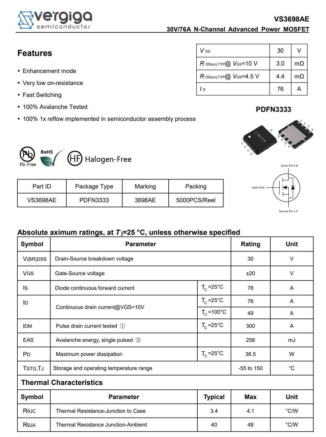
Here is the information about Vergiga VS3698AE.
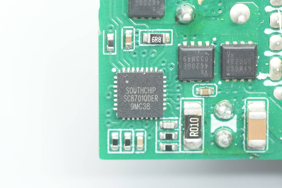
The synchronous buck-boost controller is from SouthChip, model SC8701. It is a synchronous four-MOSFET buck-boost controller that maintains a regulated output regardless of whether the input voltage is higher than, lower than, or equal to the output voltage.
The SC8701 supports a very wide input-output voltage range, with an operating range of 2.7–36 V, accommodating diverse application requirements. It also features an industry-leading 10 V gate driver voltage, maximizing the performance of external power MOSFETs to achieve optimal conversion efficiency.
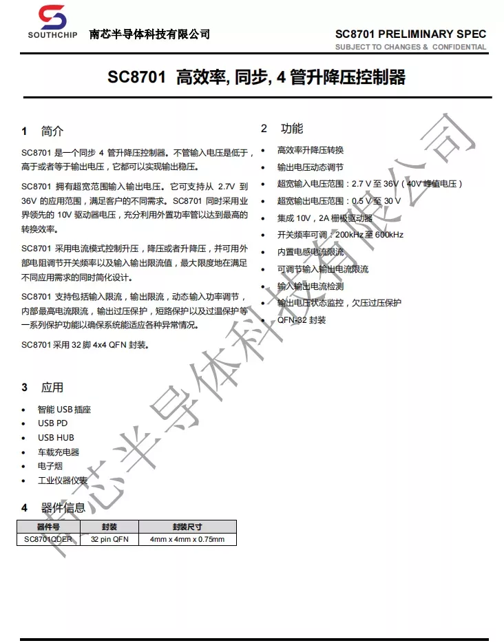
The SC8701 uses current-mode control for boost, buck, or buck-boost operation, and allows external resistors to adjust the switching frequency as well as the input and output current limits. This design maximizes flexibility for different applications while simplifying overall system design.
It supports a comprehensive set of protection features, including input current limiting, output current limiting, dynamic input power regulation, internal peak current limiting, output overvoltage protection, short-circuit protection, and over-temperature protection, ensuring reliable operation under various abnormal conditions. The device comes in a 32-pin 4×4 mm QFN package.
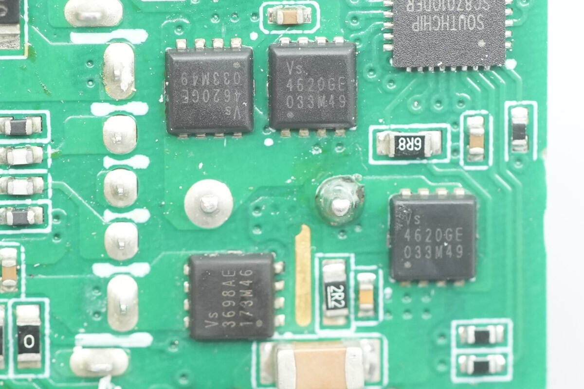
The synchronous buck-boost MOSFETs are from Vergiga, model VS4620GEMC. They are NMOS devices with a voltage rating of 40 V and an on-resistance of 6.4 mΩ, housed in a PDFN 3×3×3 package.
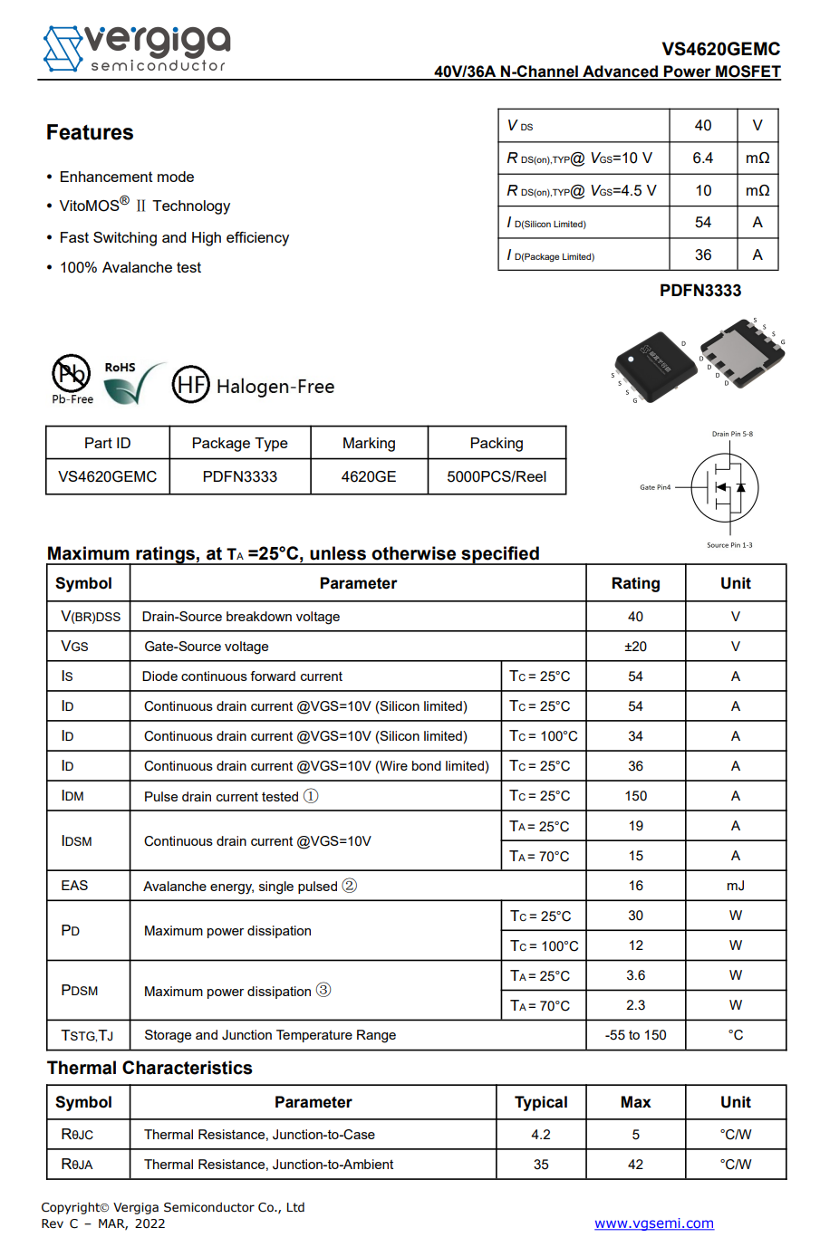
Here is the information about Vergiga VS4620GEMC.
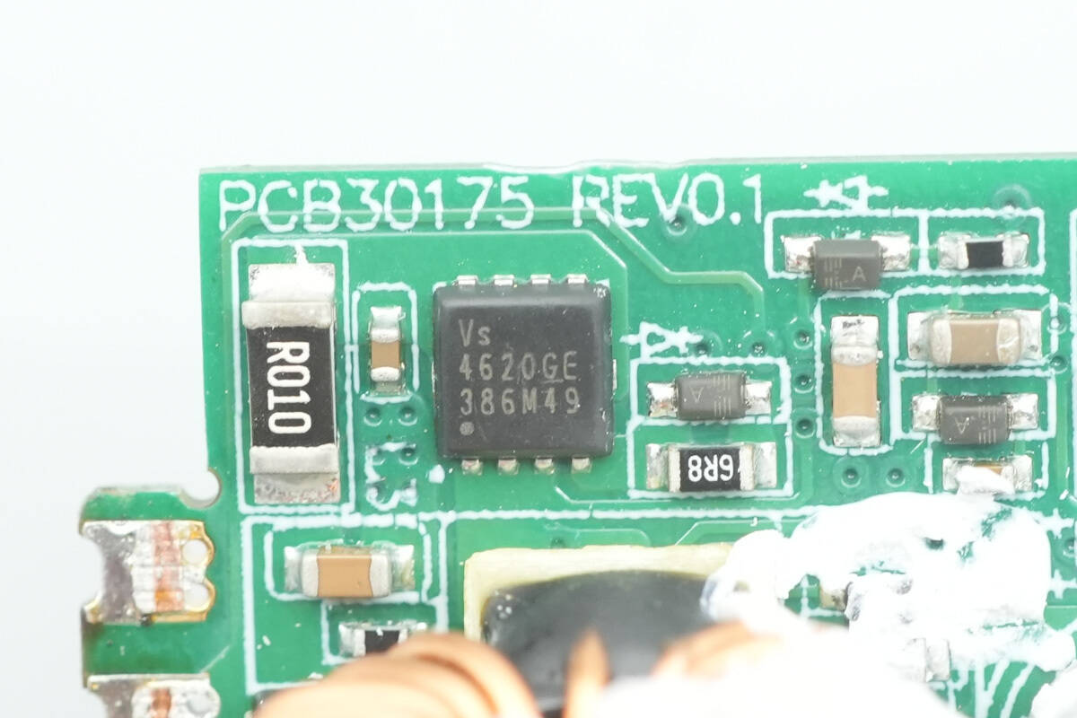
One Vergiga VS4620GEMC synchronous buck-boost MOSFET is mounted on the other side of the small PCB.
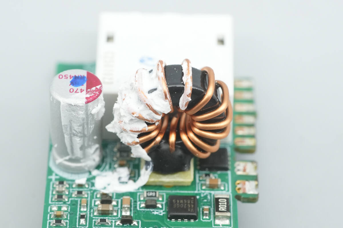
A close-up of the buck-boost inductor.
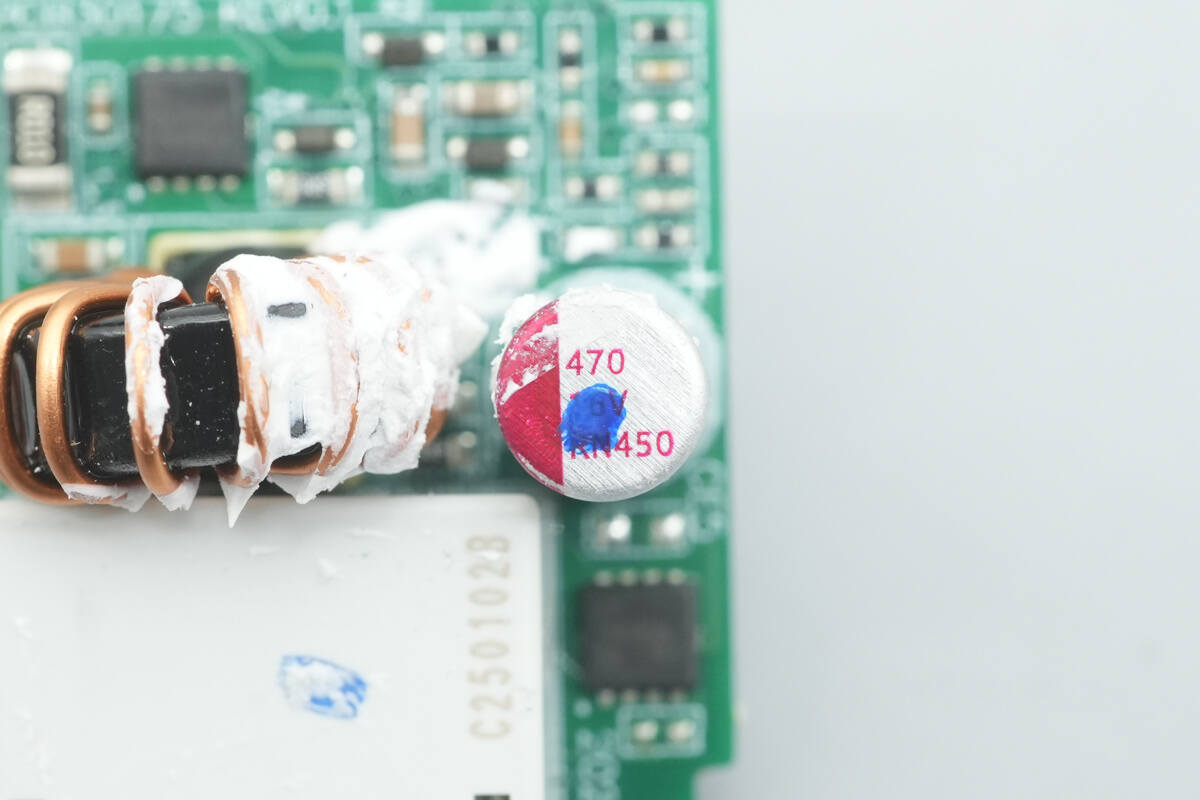
The secondary filter solid capacitor is rated at 16 V 470 μF.
The output VBUS MOSFET also uses the Vergiga VS3698AE.
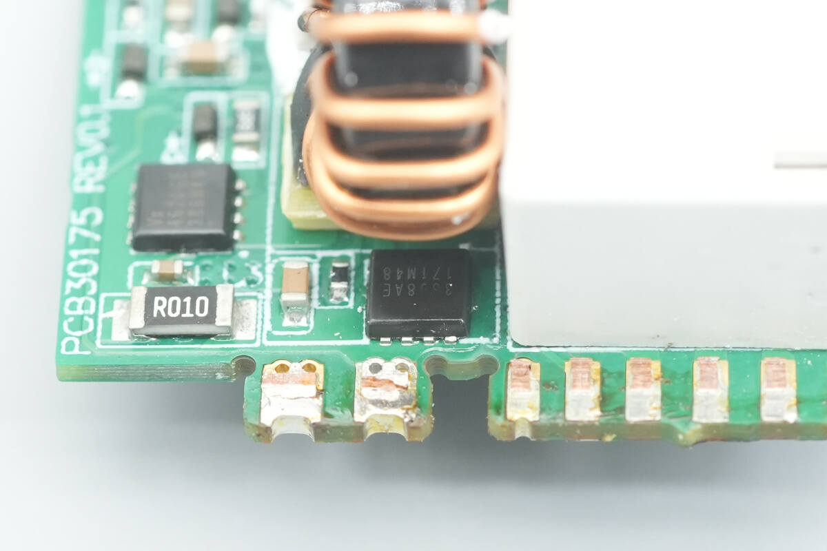
The other output VBUS MOSFET also uses the Vergiga VS3698AE.
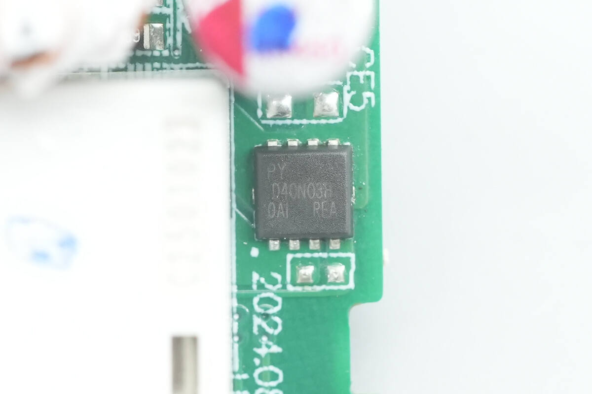
The third VBUS MOSFET is from PY, model D40N03H. It is a 30 V NMOS with an on-resistance of 4.3 mΩ, housed in a DFN 3×3 package.

Well, those are all components of the OPPO 120W SuperVOOC GaN Charger.
Summary of ChargerLAB
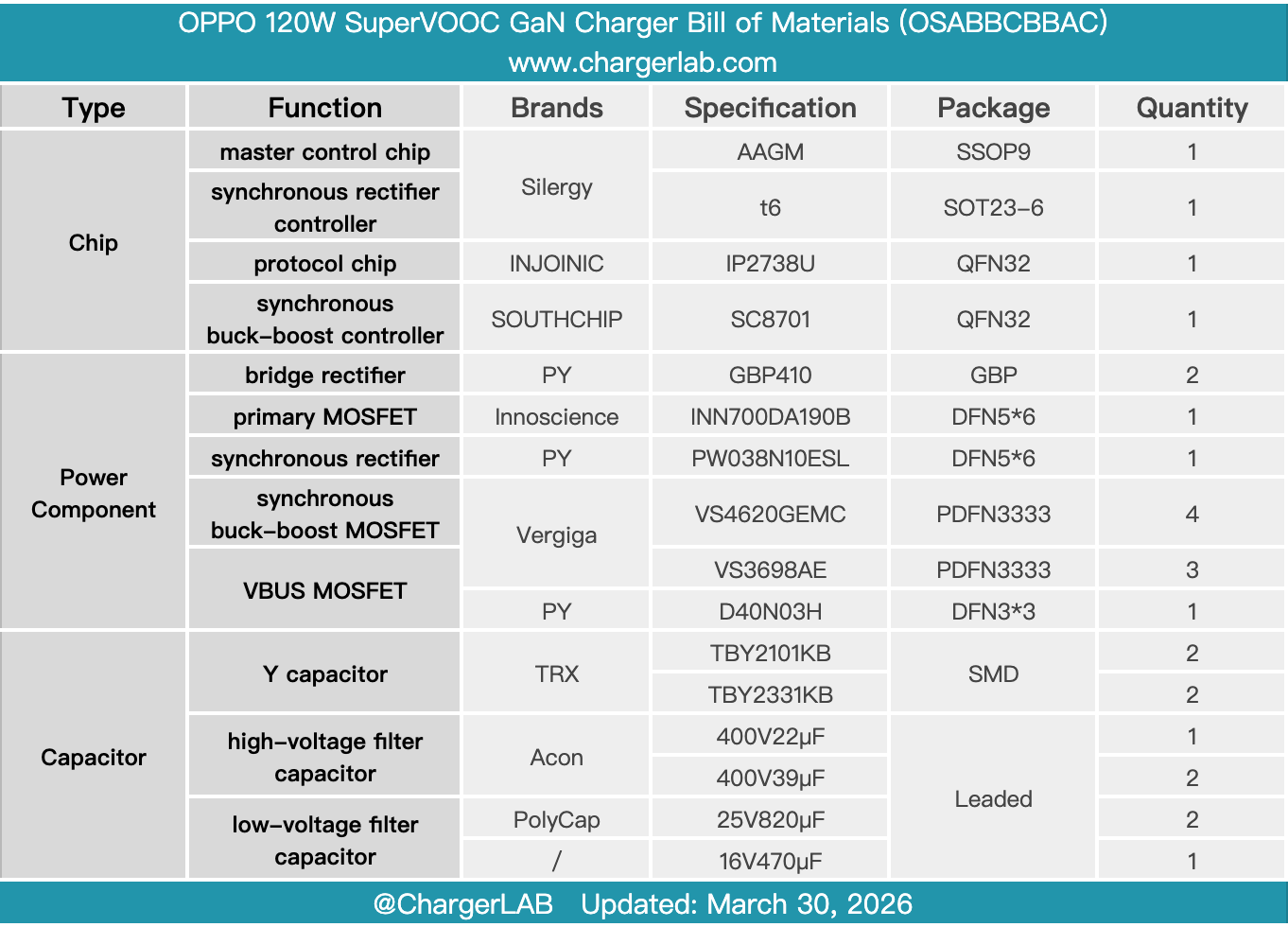
Here is the component list of the OPPO 120W SuperVOOC GaN Charger for your convenience.
It features one USB-A and one USB-C output port and is compatible with multiple protocols, including PD, PPS, and QC3.0. It can provide efficient charging for a wide range of devices such as smartphones, tablets, and laptops, offering broad compatibility and strong versatility.
After taking it apart, we found that it utilizes a high-performance power solution from Silergy, paired with the Innoscience INN700DA190B GaN power chip. It also incorporates an Injoinic protocol chip, a SouthChip synchronous buck-boost controller, and Vergiga MOSFETs, among other components. The design demonstrates solid craftsmanship in thermal management, electromagnetic shielding, and safety protection, with reliable materials and a well-structured layout.
Related Articles:
1. Teardown of OnePlus 100W SuperVOOC GaN Charger (VCBAOBCH)
2. Teardown of Anker Nano 5000mAh Magnetic Power Bank (A1665)
3. Teardown of HuntKey 45W GaN Charger (HKC04520023-0J2)