Introduction
On June 5, Nintendo launched its next-generation gaming console, the Switch 2. Compared to the previous generation, the new model features significant improvements in hardware performance, display quality, and controller design. It is equipped with a 60W fast charger, which offers a notable increase in maximum power output.
Earlier, we conducted a teardown of the original 60W charger that comes with the Switch 2. In this article, we will take apart the Japan version of the original 60W charger to examine the differences in design and materials between the two versions.
Product Appearance
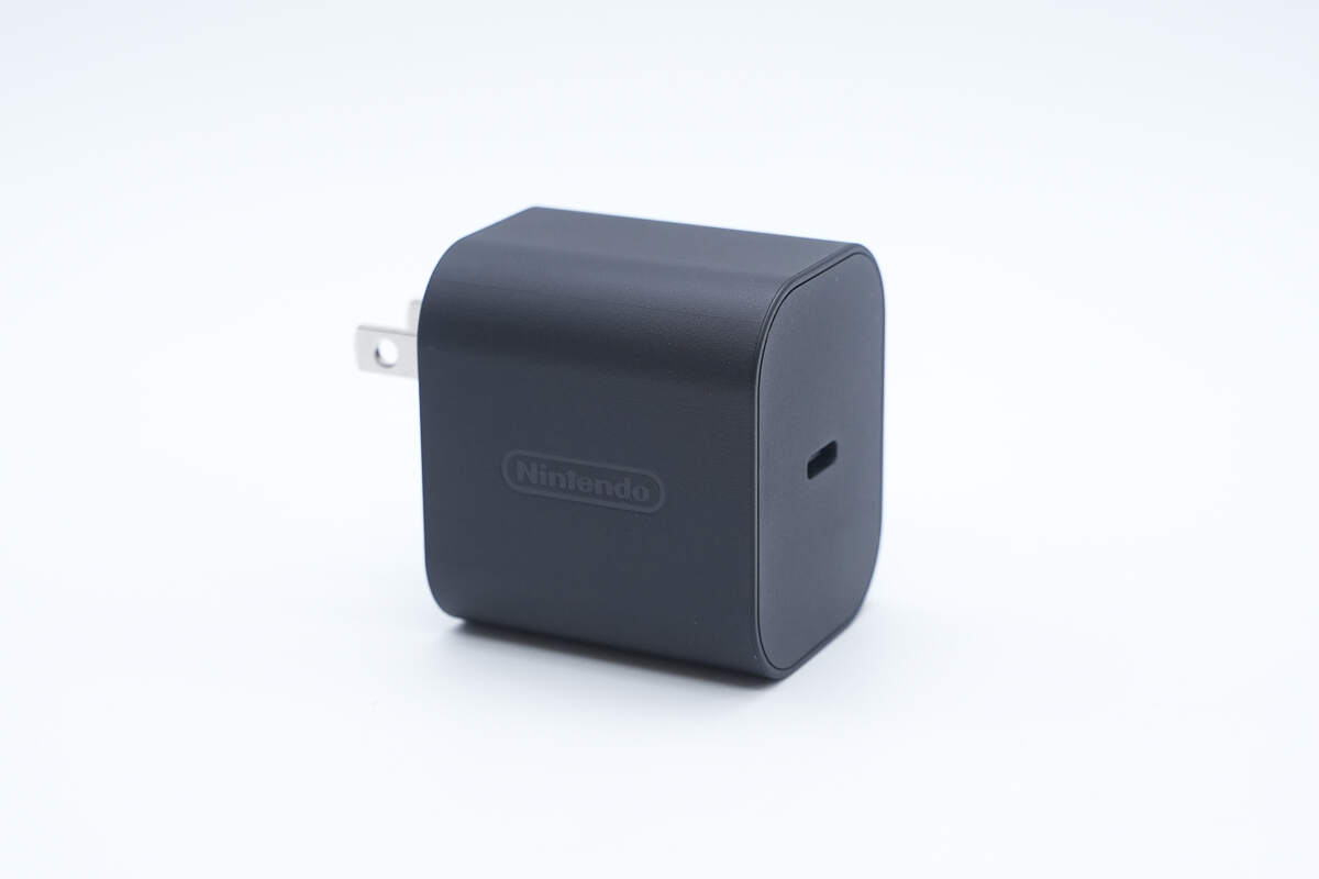
The overall design of the charger body is identical to the previously dissected version, but the input side is equipped with a Japanese standard plug.
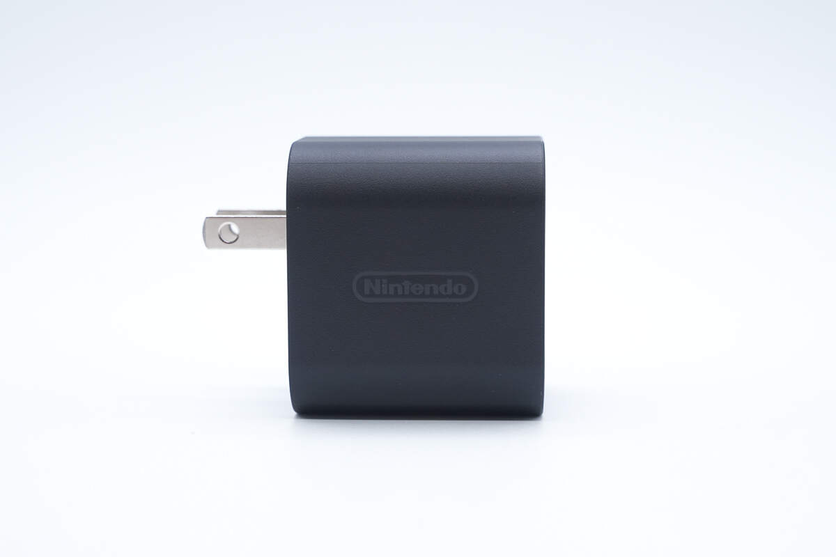
Nintendo is printed on the front of the charger.
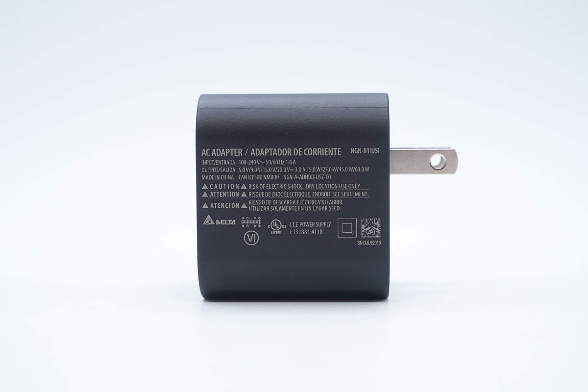
The back of the charger displays the technical specifications.

Input: 100-240V~50/60Hz 1.6A
Output: 5/9/15/20V 3A, 60W Max
Manufacturer: Delta Electronics, Inc.
The charger is UL certified and meets Level VI energy efficiency standards.
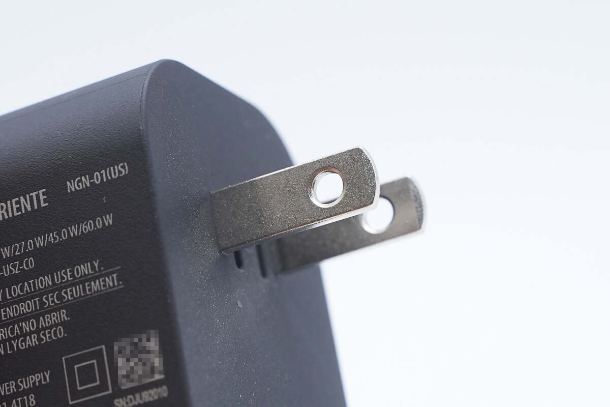
Close-up of the plug.
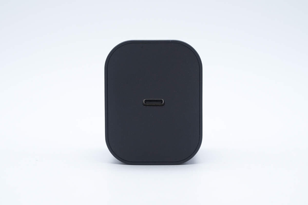
The output side features a centered USB-C port.
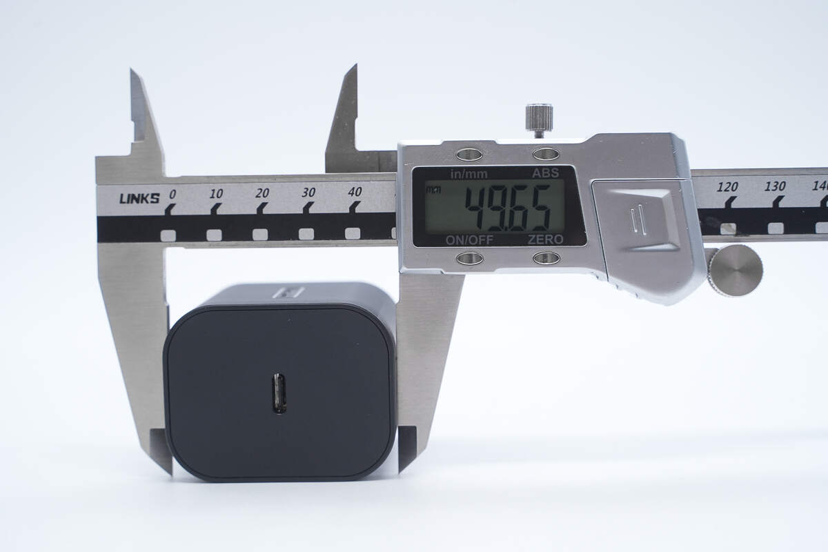
The length is about 45.05 mm (1.77 inches).
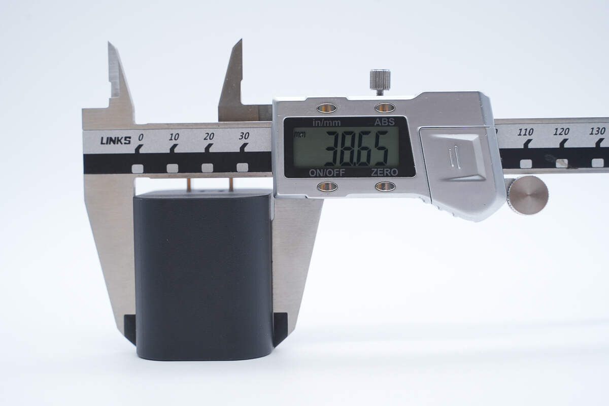
The width is about 49.65 mm (1.95 inches).
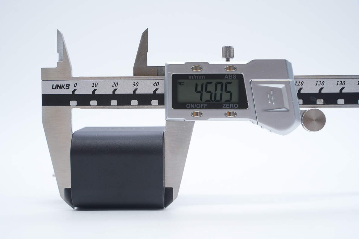
The thickness is about 38.65 mm (1.52 inches).
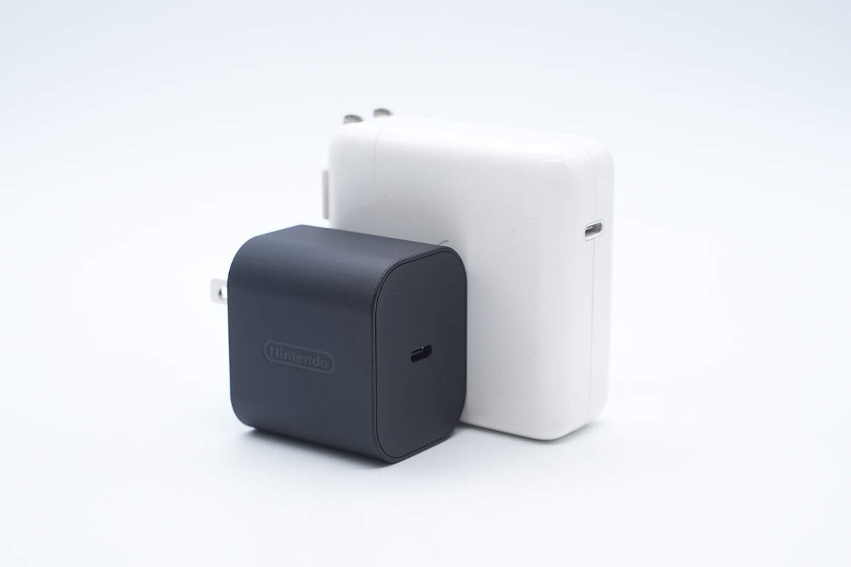
It is much smaller than the Apple 61W charger.
That's how big it is in the hand.
The weight is about 117 g (4.13 oz).
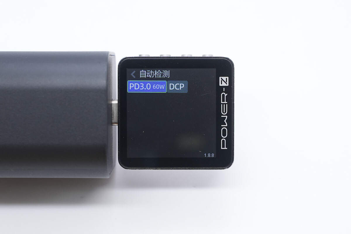
ChargerLAB POWER-Z KM003C shows it supports PD3.0 and DCP protocols.
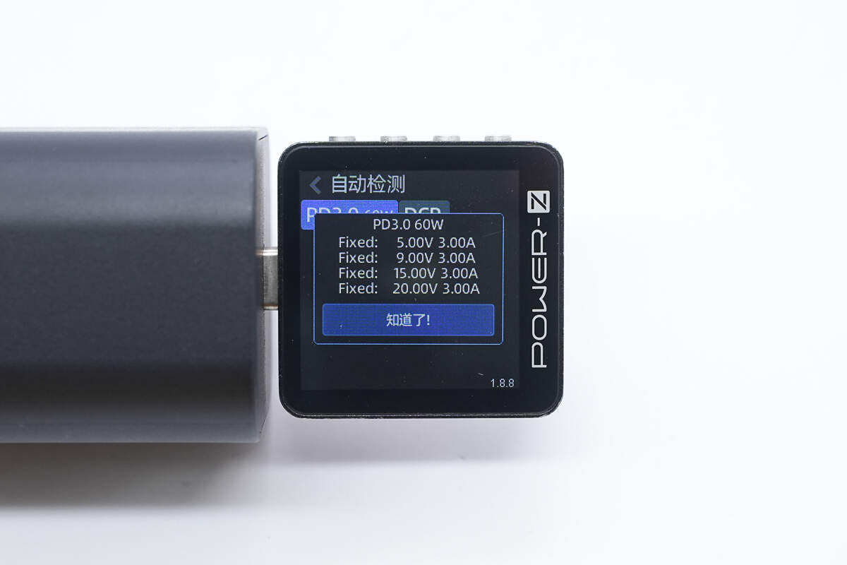
It has four fixed PDOs of 5V3A, 9V3A, 15V3A, and 20V3A.
Teardown
Next, let's take it apart to see its internal components and structure.
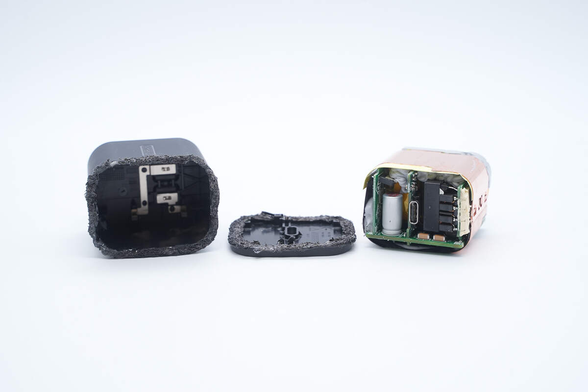
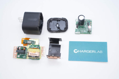
Cut open the top cover. The input uses a contact-based power connection design.
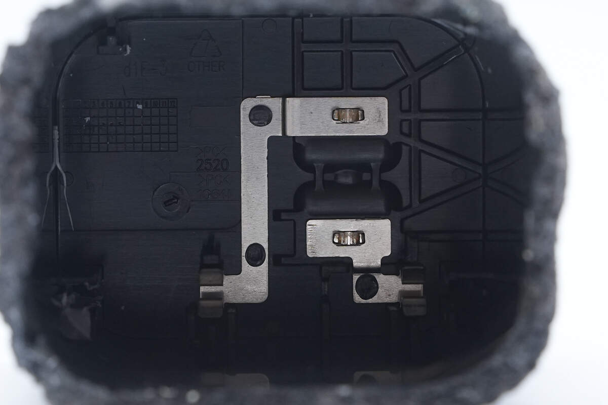
The metal spring clips are crimped onto the plug pins.
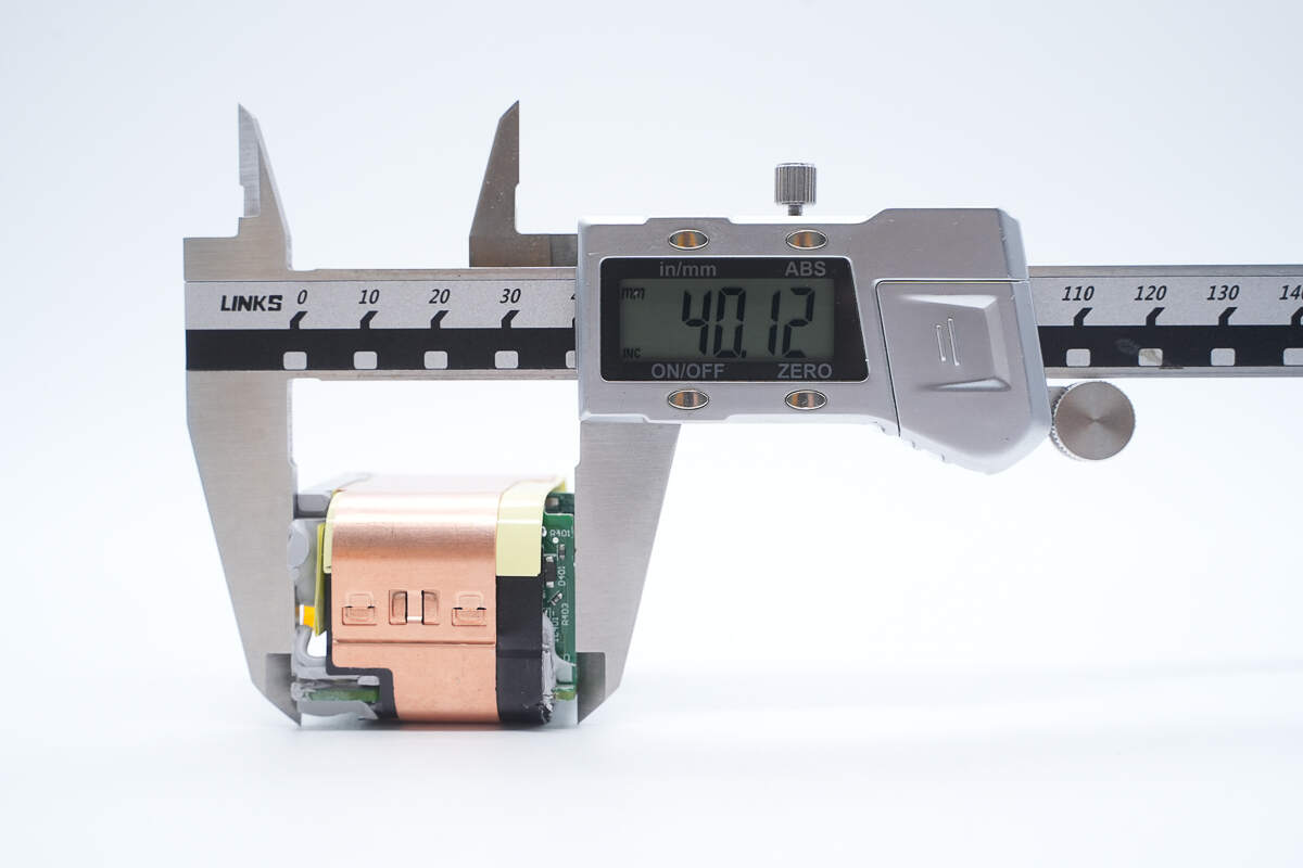
The length of the PCBA module is about 40.12 mm (1.58 inches).
The width is about 44.47 mm (1.75 inches).
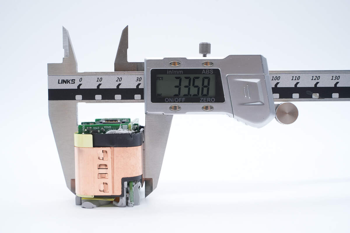
The thickness is about 33.58 mm (1.32 inches).
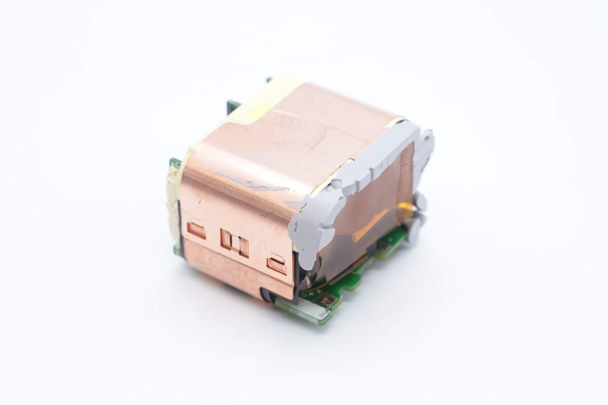
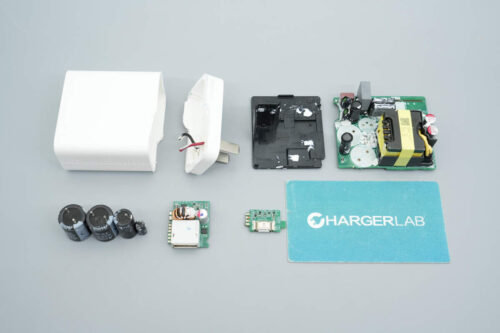
The PCBA module is wrapped in a copper heat sink and secured with a snap-on structure. The input end is glued, and a high-temperature-resistant insulation sheet is attached.
The copper heat sink is also fixed with screws and has Mylar sheets on the inside for insulation.
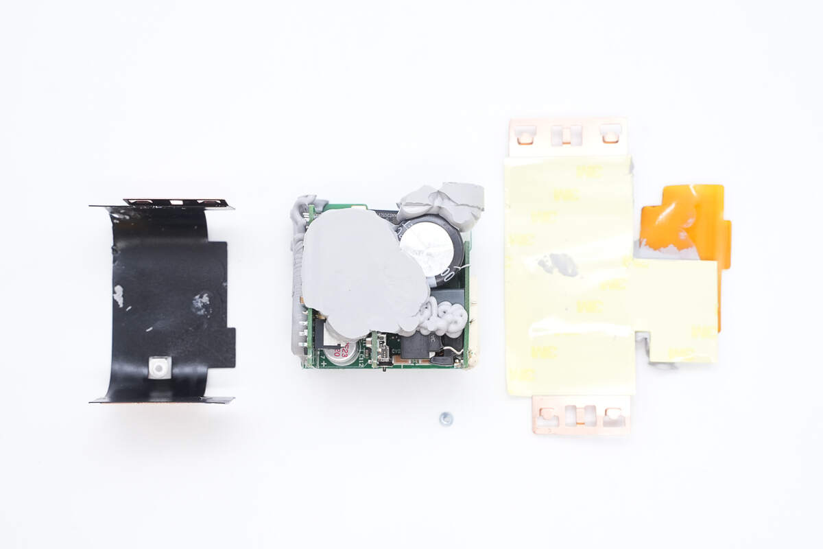
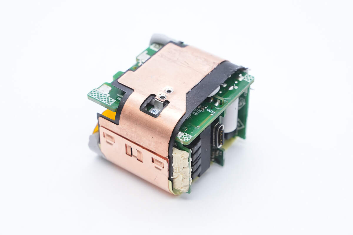
Remove the heat sink, and you'll find insulation tape applied to the inner side.
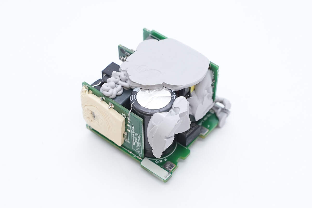
Thermal compound is applied to the PCBA module, and a thermal pad is attached to the small PCB on the side.

The back side is also filled with thermal compound, and a Mylar sheet is placed in the cutout between the primary and secondary sides for isolation.
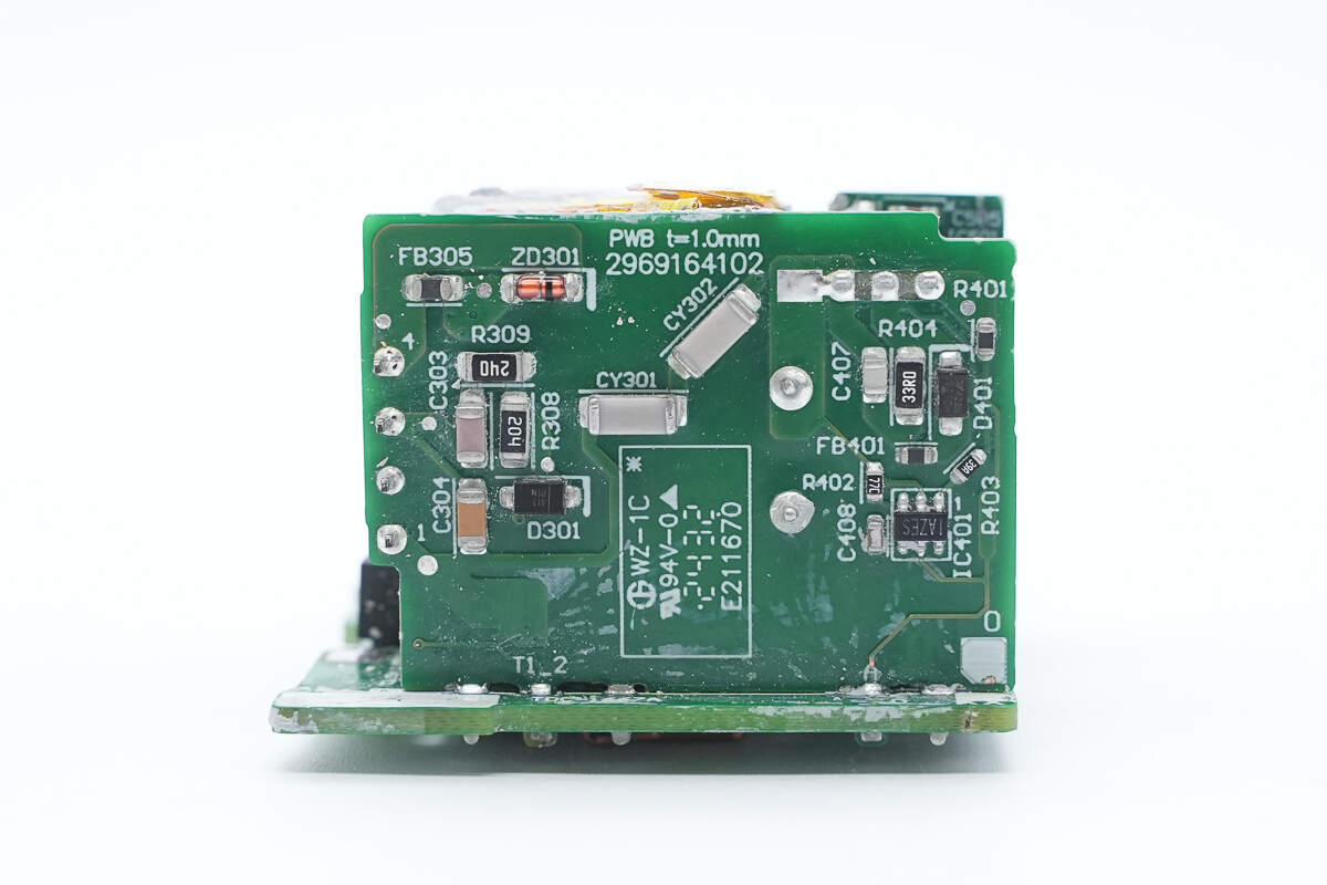
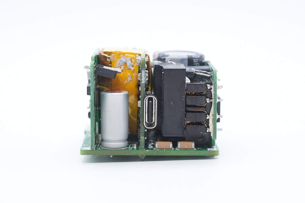
After removing the thermal compound, multiple stacked PCBs can be seen in the module, making efficient use of the internal space.
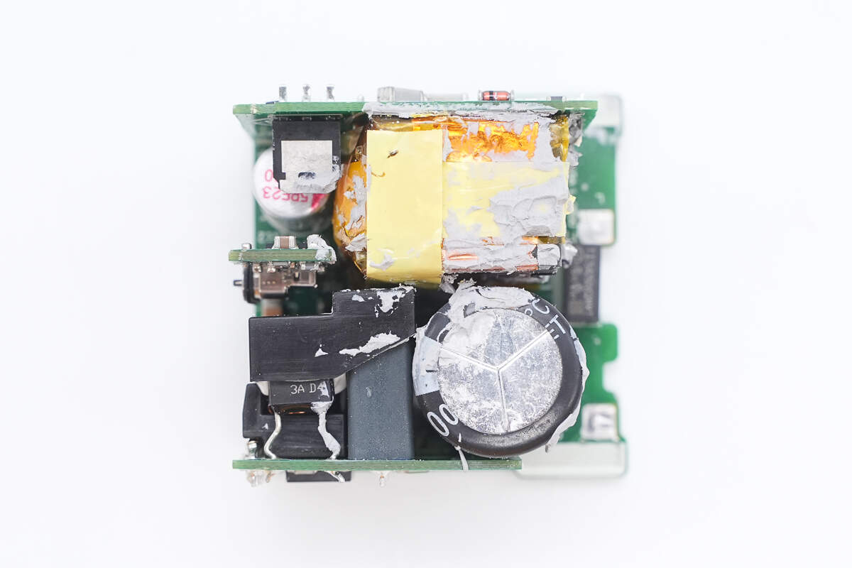
The area between the two small PCBs houses components such as the electrolytic capacitor and the transformer. The side with the output connector features a plastic casing for insulation and isolation.
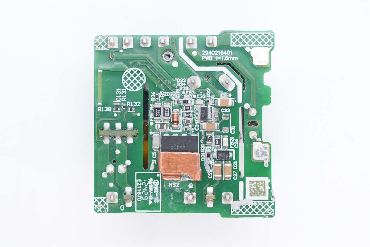
On the back side, the primary controller chip and primary MOSFET are located, with the MOSFET covered by a copper heatsink.
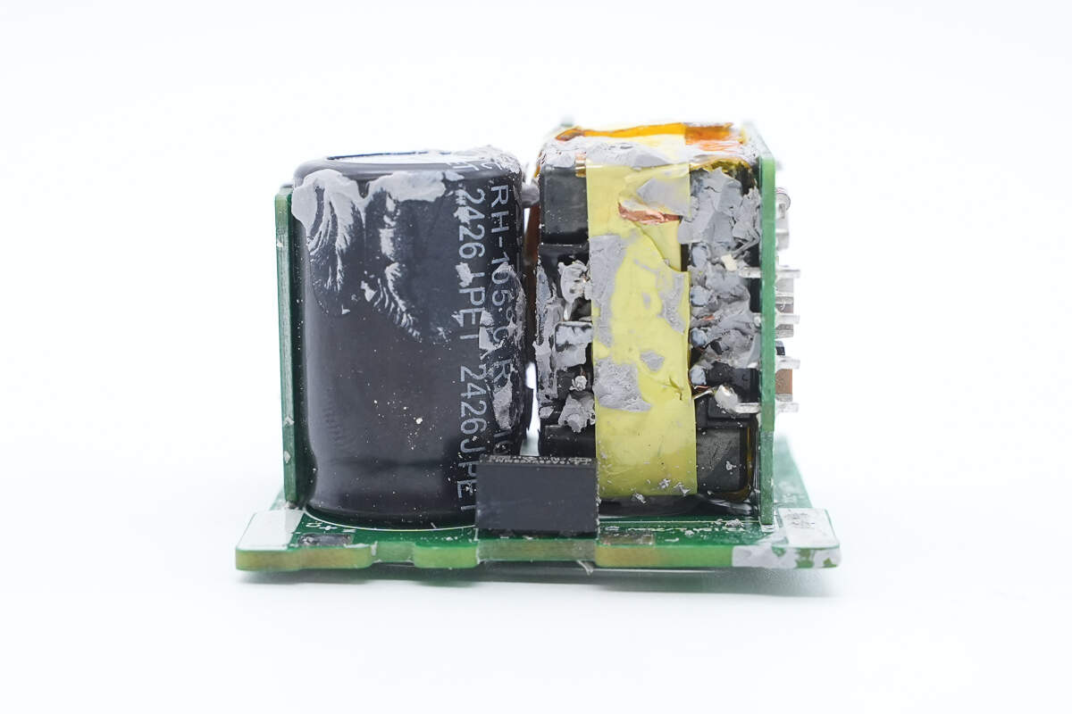
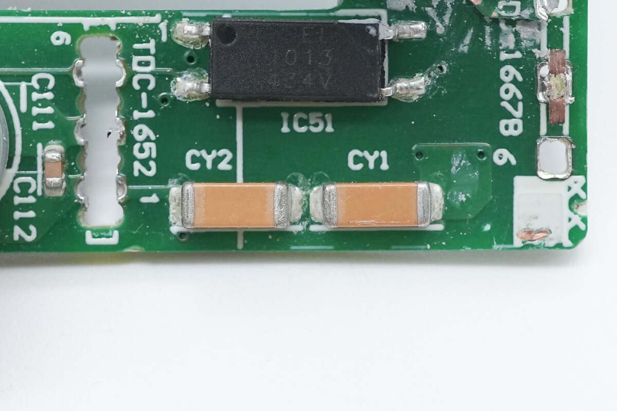
The input side includes a time-delay fuse and a high-voltage filtering electrolytic capacitor.

The back side of this small PCB features a bridge rectifier.
Remove the small PCB. The components on the front are covered with a plastic casing.
Remove the plastic casing. White adhesive is applied to the components.

The time-delay fuse is rated at 3.15A 250V.
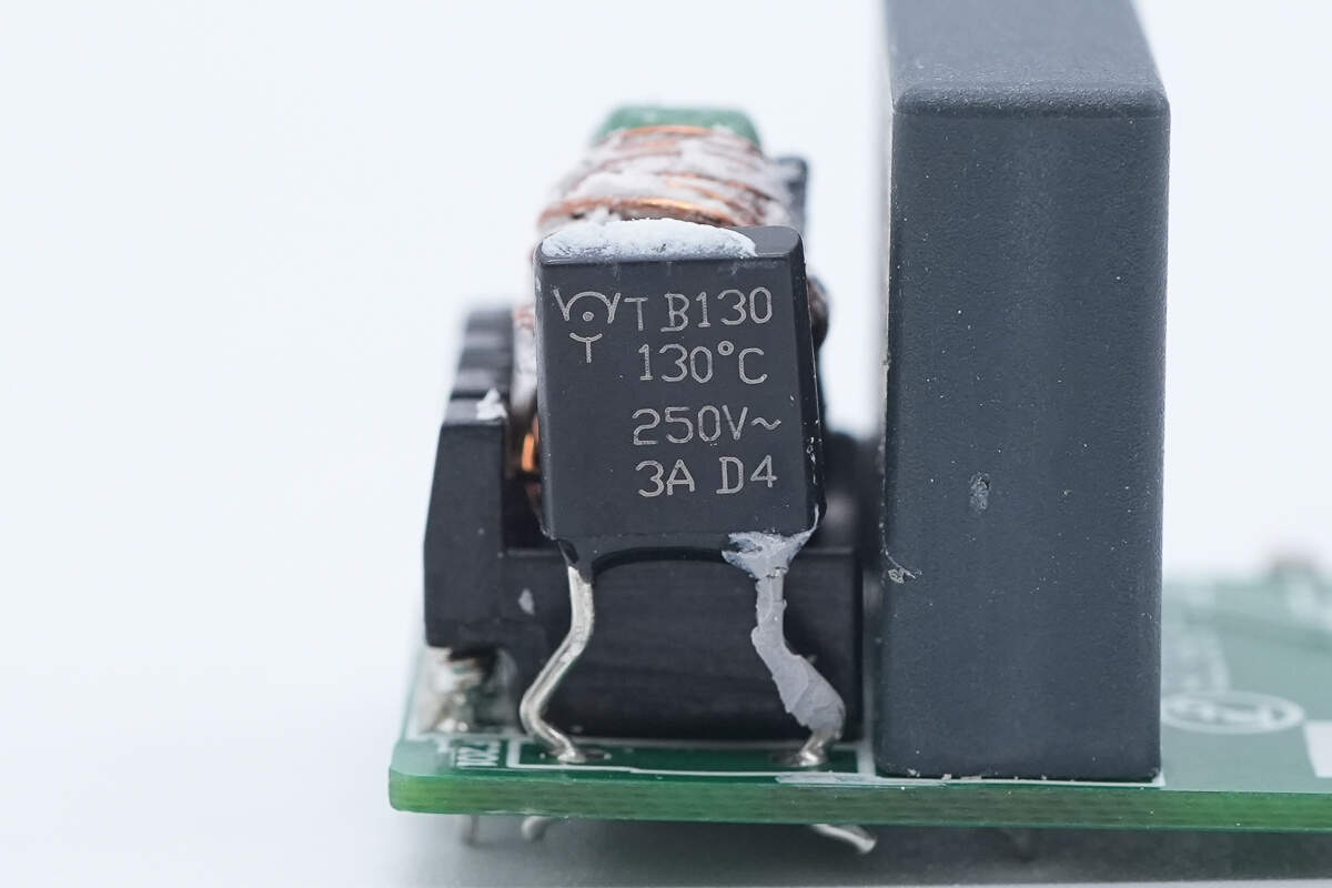
The thermal fuse is manufactured by WalterFuse.

The common mode choke is used to filter out EMI interference.
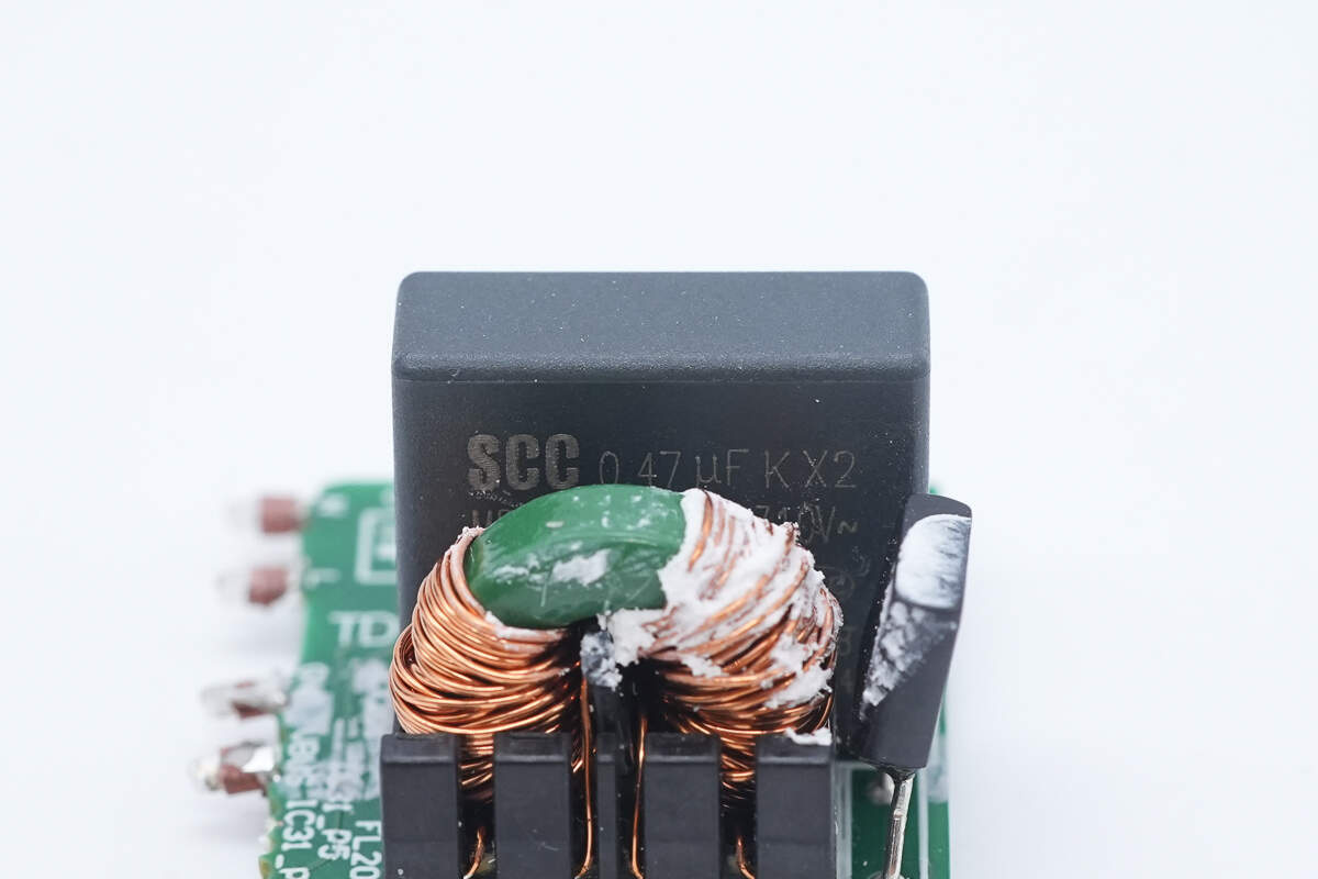
The safety X2 capacitor is from SCC, with a specification of 0.47μF.
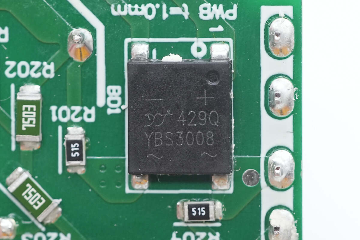
The bridge rectifier is from YJ, model YBS3008, rated at 3A 800V, and uses a YBS package.
The back side of the other small PCB features a synchronous rectifier controller.
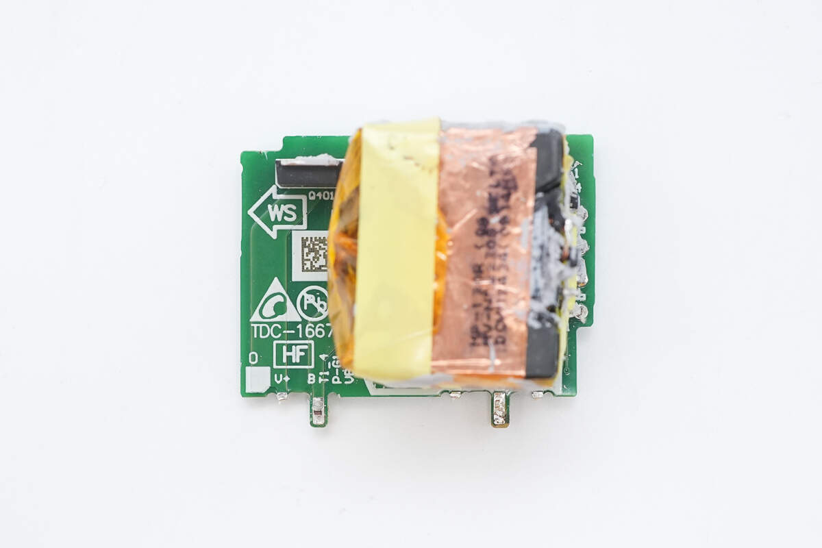
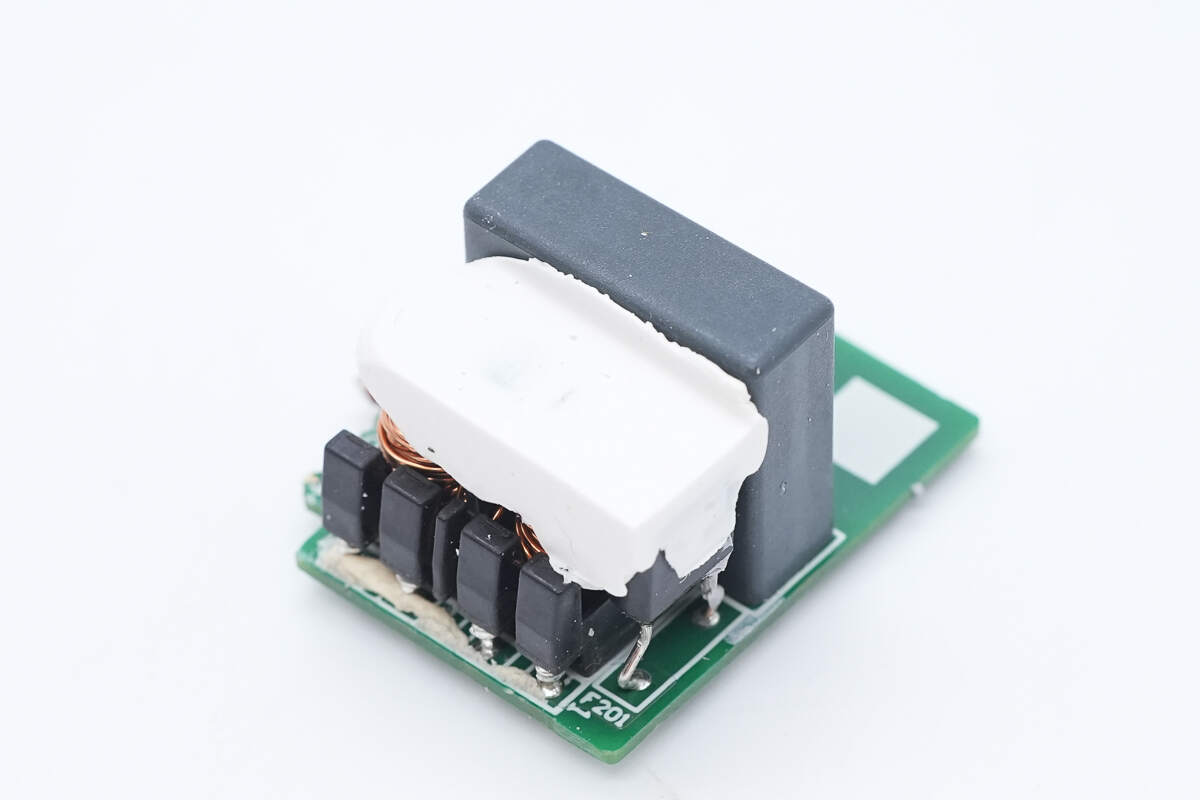
Remove the small PCB. On the other side, there is a transformer and a synchronous rectifier.
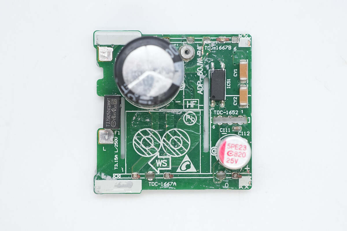
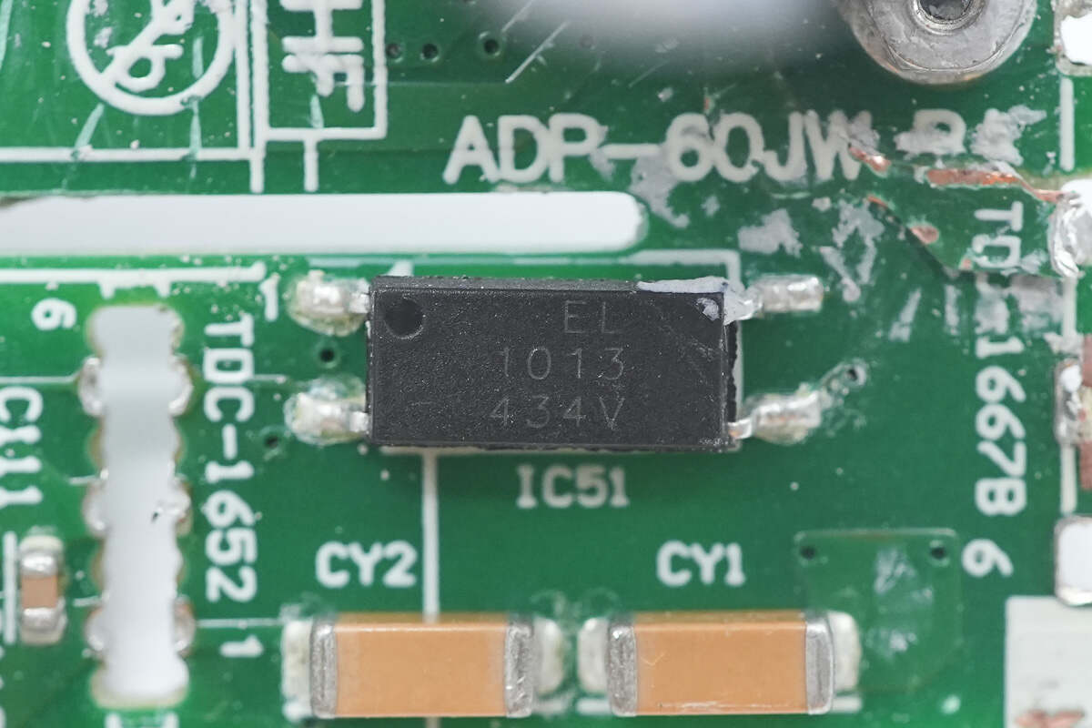
After removing all the small PCBs from the front, the main PCB front side contains an optocoupler, SMD Y capacitors, one electrolytic capacitor, and one solid output filter capacitor.
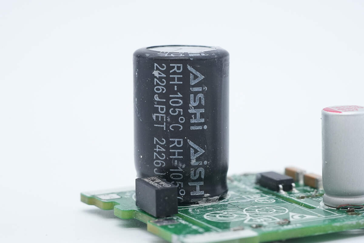
The electrolytic capacitor is from AiSHi.
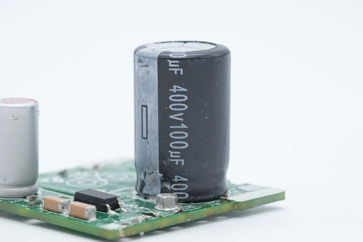
It is rated at 400V 100μF.
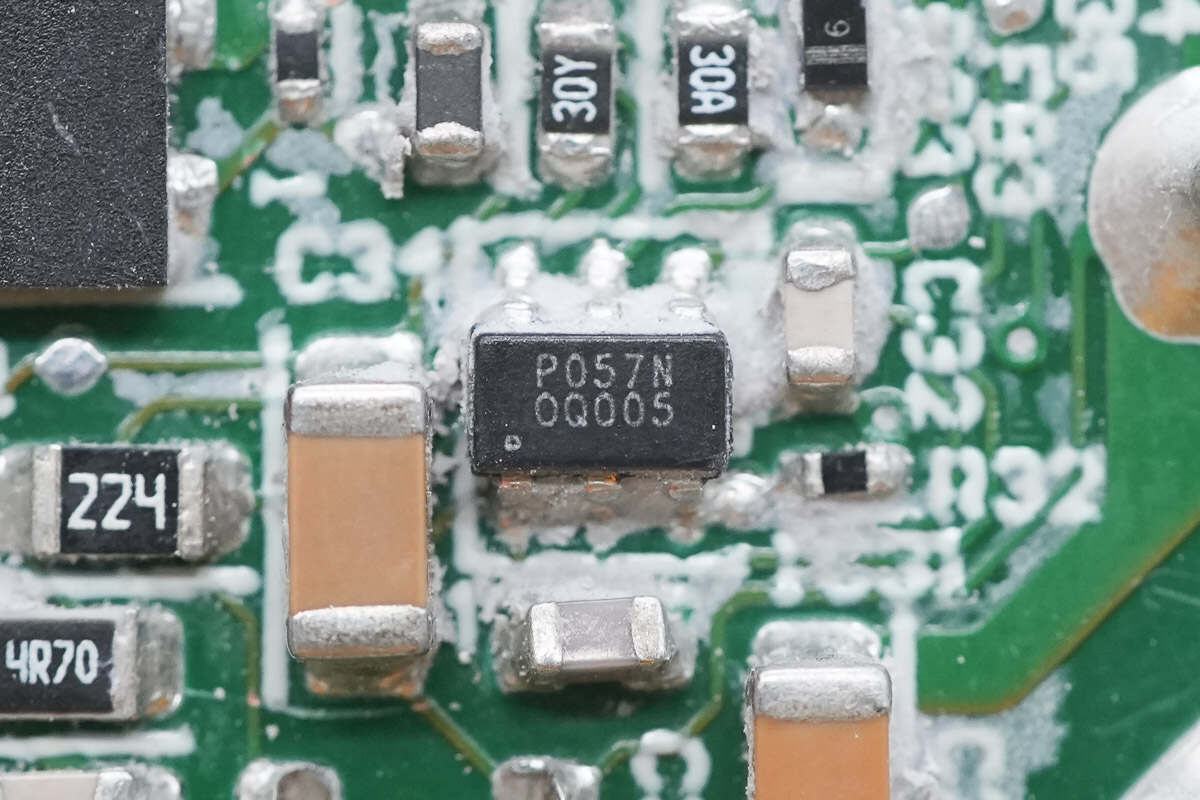
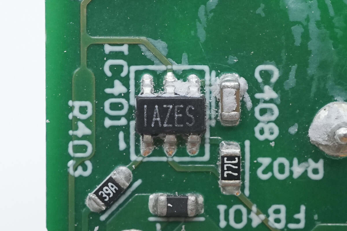
The primary controller chip is marked with P057N and comes in a SOT-23-6 package.

The primary MOSFET is from Infineon, model IPL60R185P7, part of the CoolMOS P7 series. It has a voltage rating of 650V, an on-resistance of 185mΩ, and comes in a VSON-4 package.
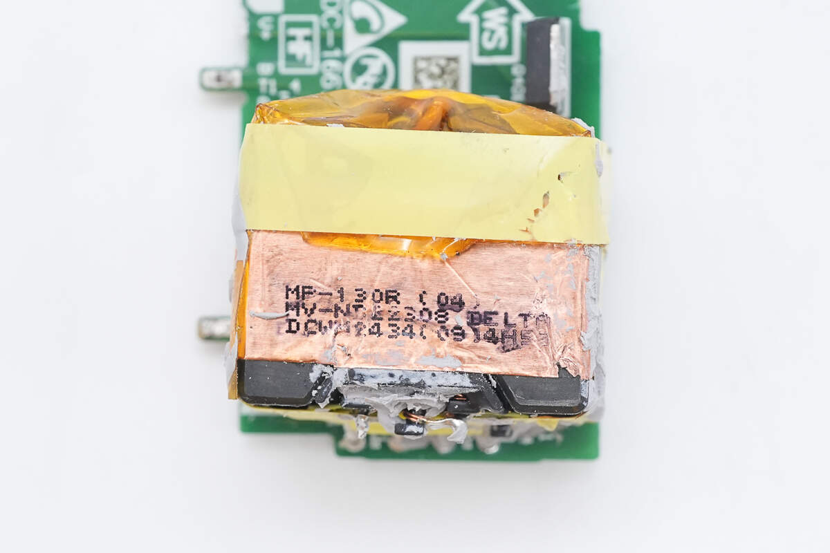
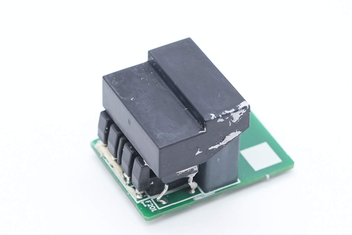
The transformer is wrapped with copper foil and insulation tape.
The Everlight EL1013 optocoupler is used for output voltage feedback.
Two SMD Y capacitors are connected in series to increase the voltage rating.
The synchronous rectifier controller is from MPS, model MP6908. It supports a wide output voltage range, multiple operating modes including DCM, CCM, and quasi-resonant, and features both high-side and low-side synchronous rectification.
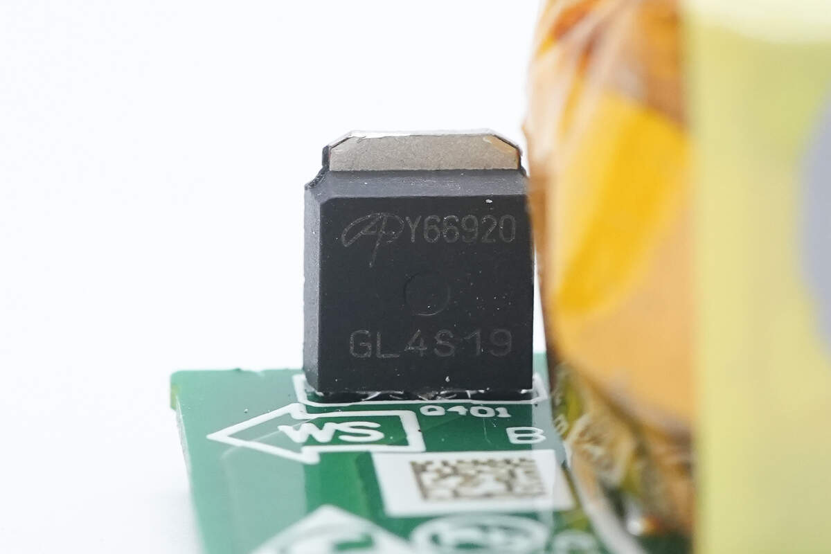
The synchronous rectifier is from AOS, model AOY66920, rated at 100V with an on-resistance of 8.2mΩ, and comes in a TO-251B package.

Here is the information about AOS AOY66920.
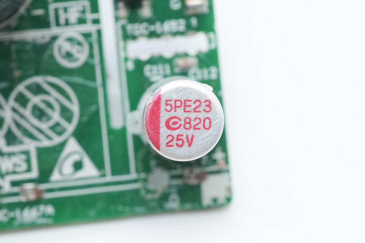
The solid capacitor for output filtering is from APAQ, rated at 25V 820μF.
The USB-C socket PCB is soldered at the center of the output end.
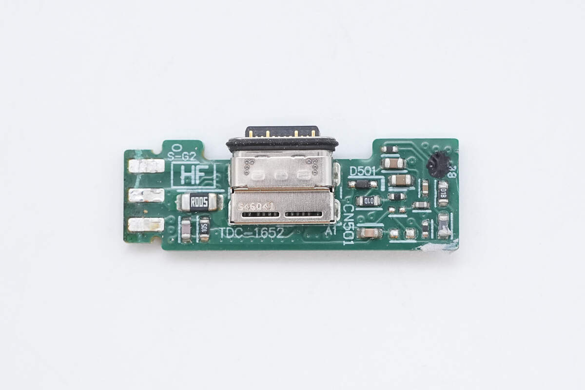
The USB-C socket is soldered on the front side of the small PCB.
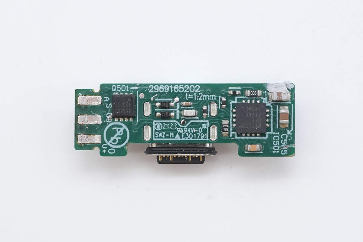
The back side features a protocol chip and an output VBUS MOSFET.
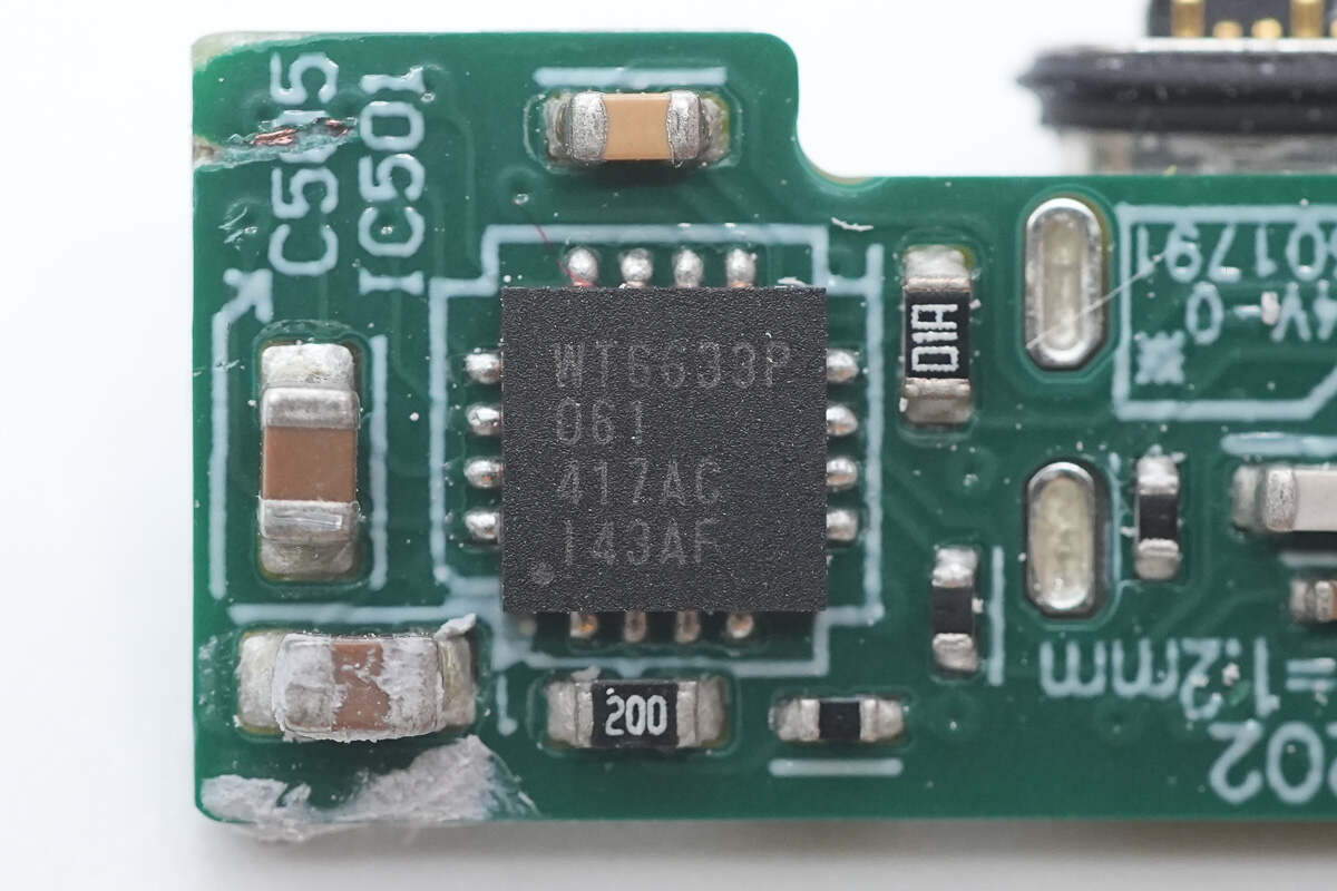
The protocol chip is from Weltrend, model WT6633P. It supports USB PD 3.0 as well as Qualcomm QC4, QC4+, and QC5 protocols. It is USB-IF certified with TID 1070018 and has Qualcomm QC5 certification (ID 4789627043-2) and QC4+ certification (ID 4788566324-2). The chip features a built-in 8051 core, integrated constant voltage and constant current control, output current sensing, line loss compensation, and comprehensive protection functions.

The output VBUS MOSFET is from APEC, model AP3NA4R2YT. It is an N-channel MOSFET rated at 30V with an on-resistance of 4.2mΩ, housed in a PMP3×3 package.
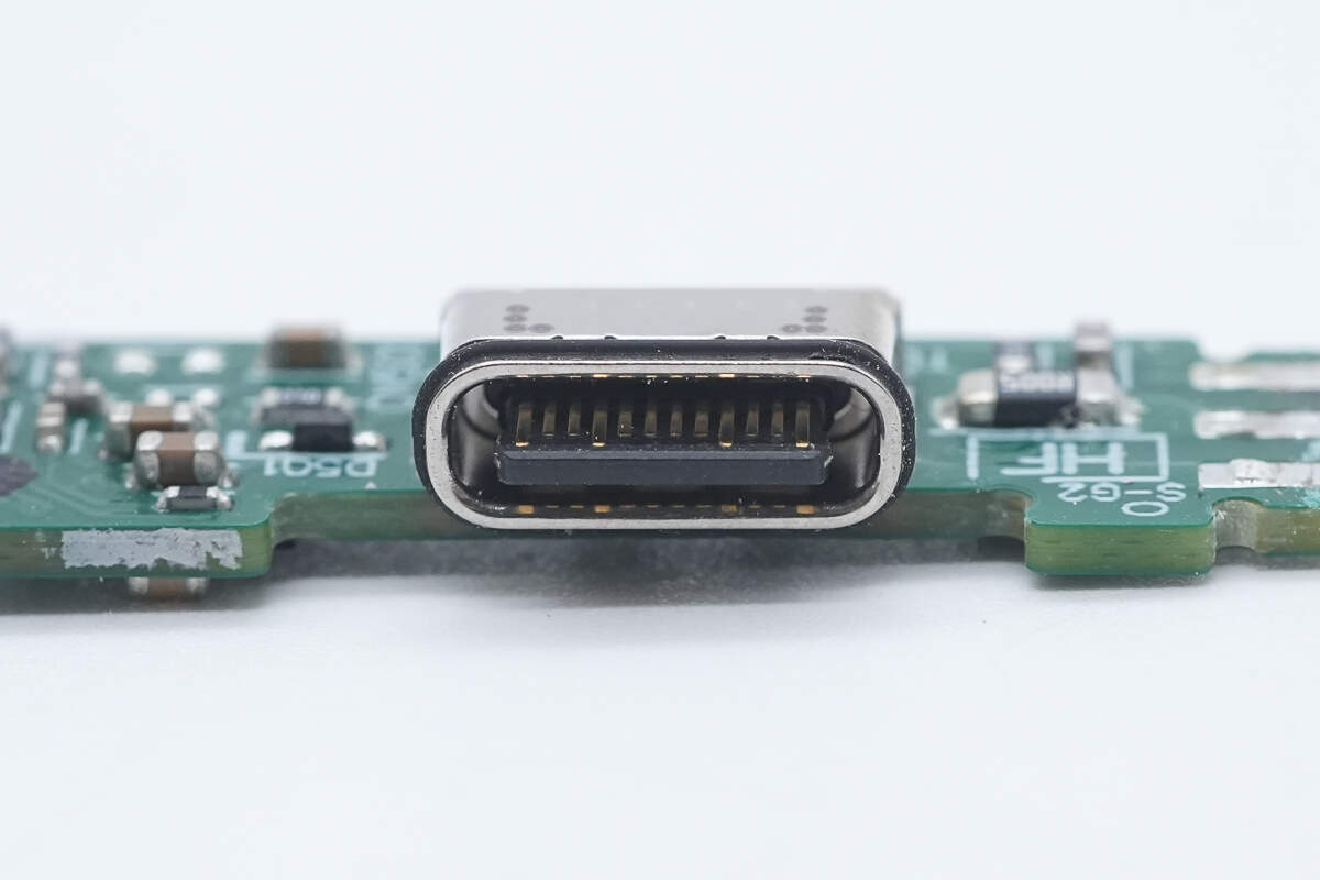
The USB-C socket is reinforced with a steel shell.

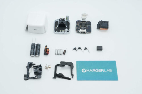
Well, those are all components of the Nintendo Switch 2 Original 60W PD Fast Charger (Japan Version).
Summary of ChargerLAB

Here is the component list of the Nintendo Switch 2 Original 60W PD Fast Charger (Japan Version) for your convenience.
Its design style is the same as the version we previously disassembled, with differences only in the plug and the branding and label layout on the body. Testing confirmed that this charger also supports PD 3.0 and can deliver a maximum output of 60W. Besides powering the Switch 2, it can also be used to charge smartphones, tablets, and even ultraportable laptops.
After taking it apart, we found that the internal module design is identical to the previous version, including the chips' and capacitors' part numbers. It is also manufactured by Delta Electronics. The PCBA module is filled with potting compound and equipped with copper heat sinks for cooling, ensuring excellent material quality and craftsmanship.
Related Articles:
1. Teardown of Google 25W Qi2.2 Magnetic Wireless Charger (GH5UG)
2. Teardown of Apple 25W Qi2.2 + MagSafe Charger A3502 (HK Version)
3. Teardown of EcoFlow RAPID 170W 25000mAh Power Bank (EF-HB-002)