Introduction
Nintendo has released its next-generation gaming console, the Switch 2, featuring significant upgrades in hardware performance, display quality, and controller design. In this article, we’ll take a closer look at the teardown of the official charging dock — one of the core accessories for the Switch 2.
Beyond serving as a charging station and a resting place for the console when not in use, the dock also supports 4K resolution output in TV mode and comes equipped with a gigabit Ethernet port for faster and more stable online gameplay. Let’s take it apart to see its internal components and structure.
Product Appearance
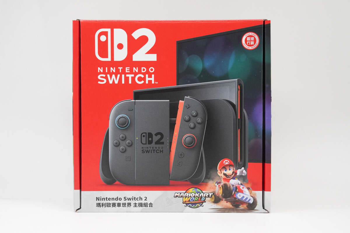
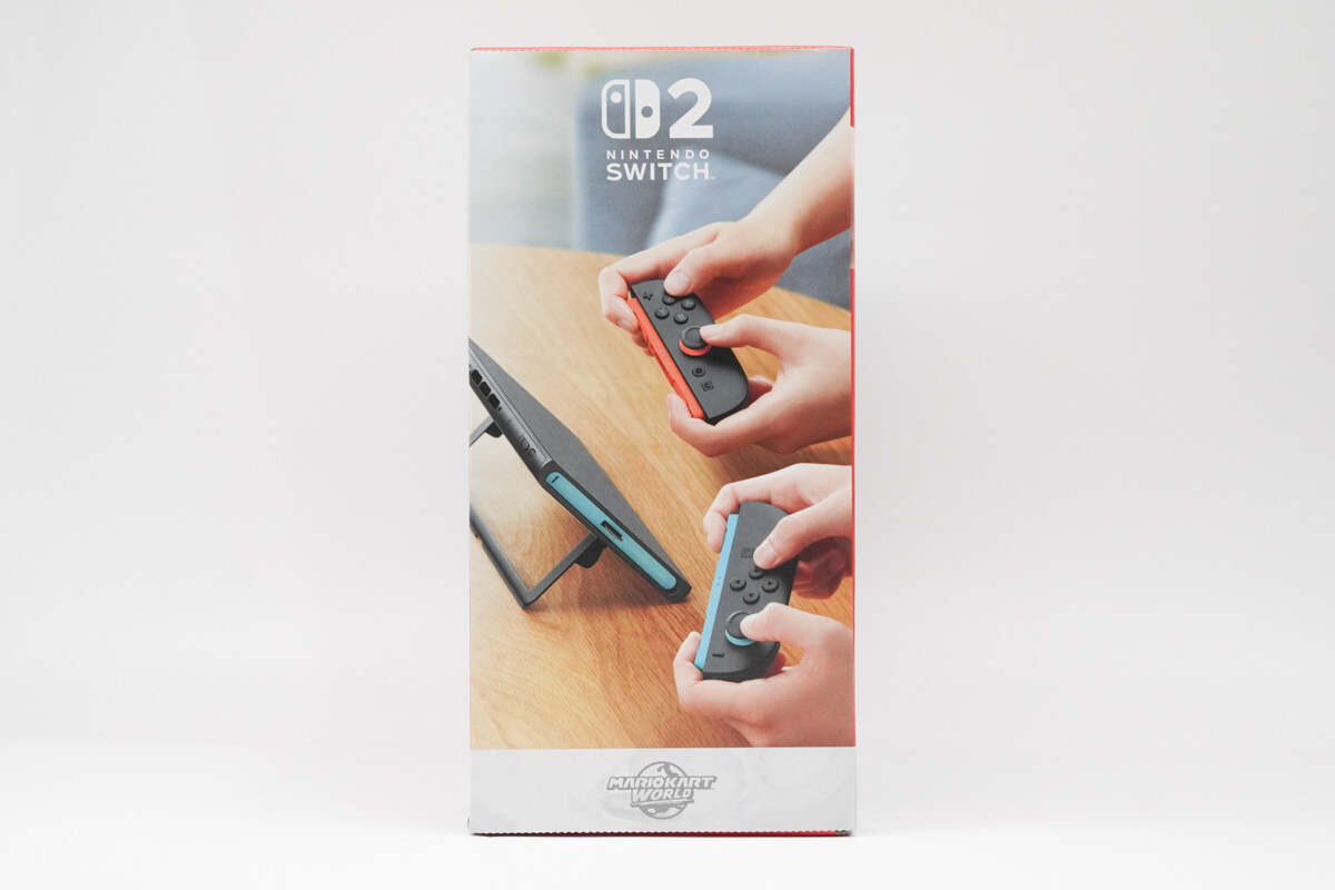
The packaging continues the classic red theme, with the front featuring images of the product itself as well as elements from Mario Kart and other related graphics.
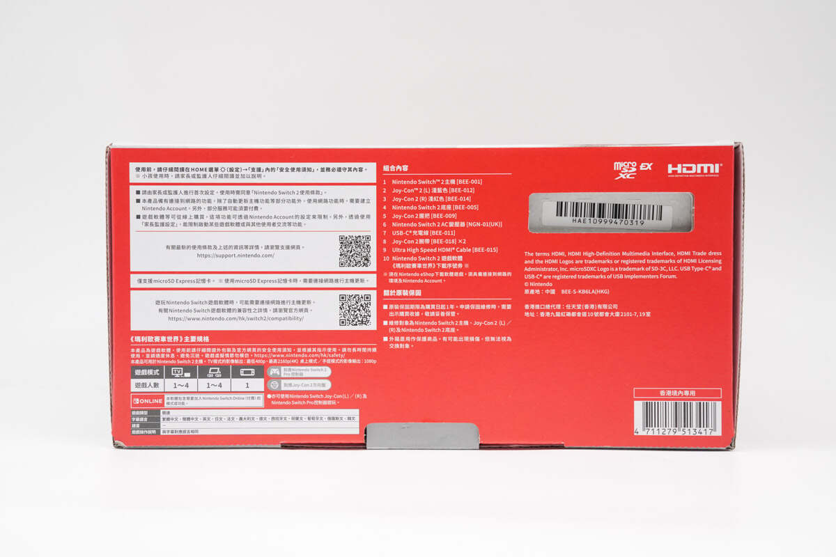
The packing list and precautions are printed on the side.
The other side is printed with product usage scenarios.
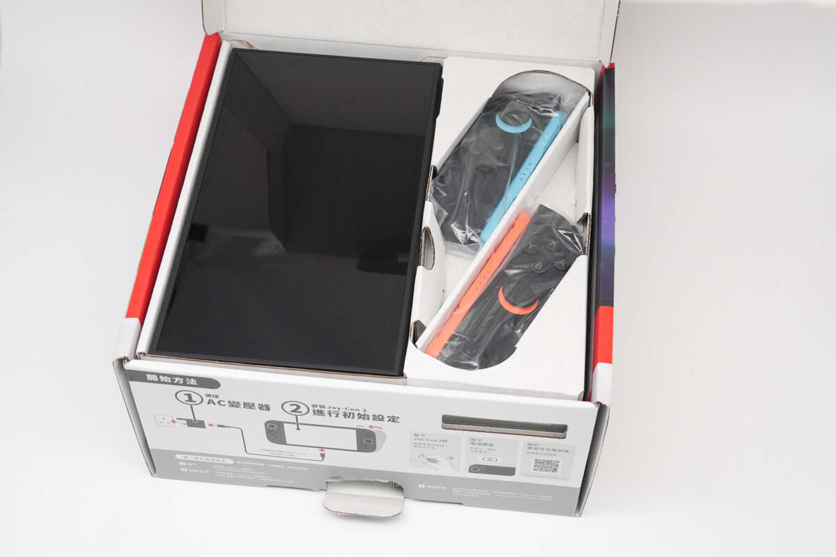
The Nintendo Switch 2 is secured with cardboard.
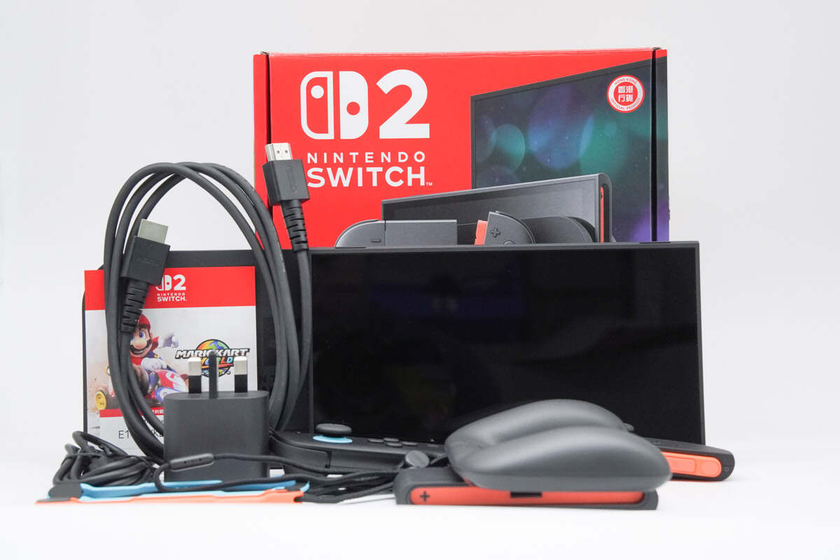
The package includes the Switch 2 console, Joy-Con set, dock, charger kit, HDMI cable, and more.
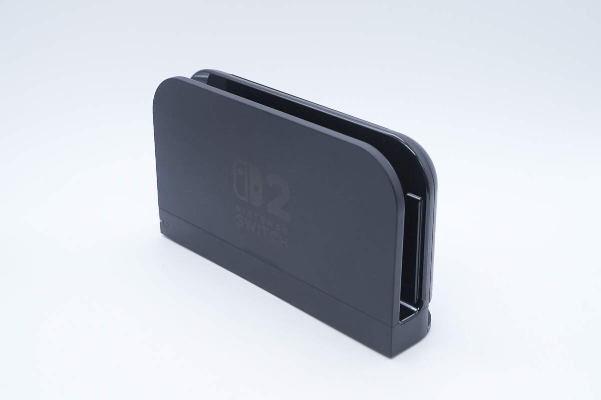
The official charging dock continues the minimalist design style, featuring a contrast of matte and glossy finishes on the surface and inside the slot.
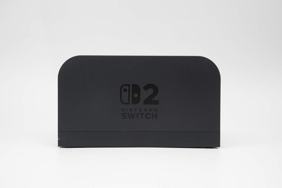
The front-facing logo is noticeably larger, and the curves at both ends of the top are more pronounced — subtle details that set it apart from the previous model.
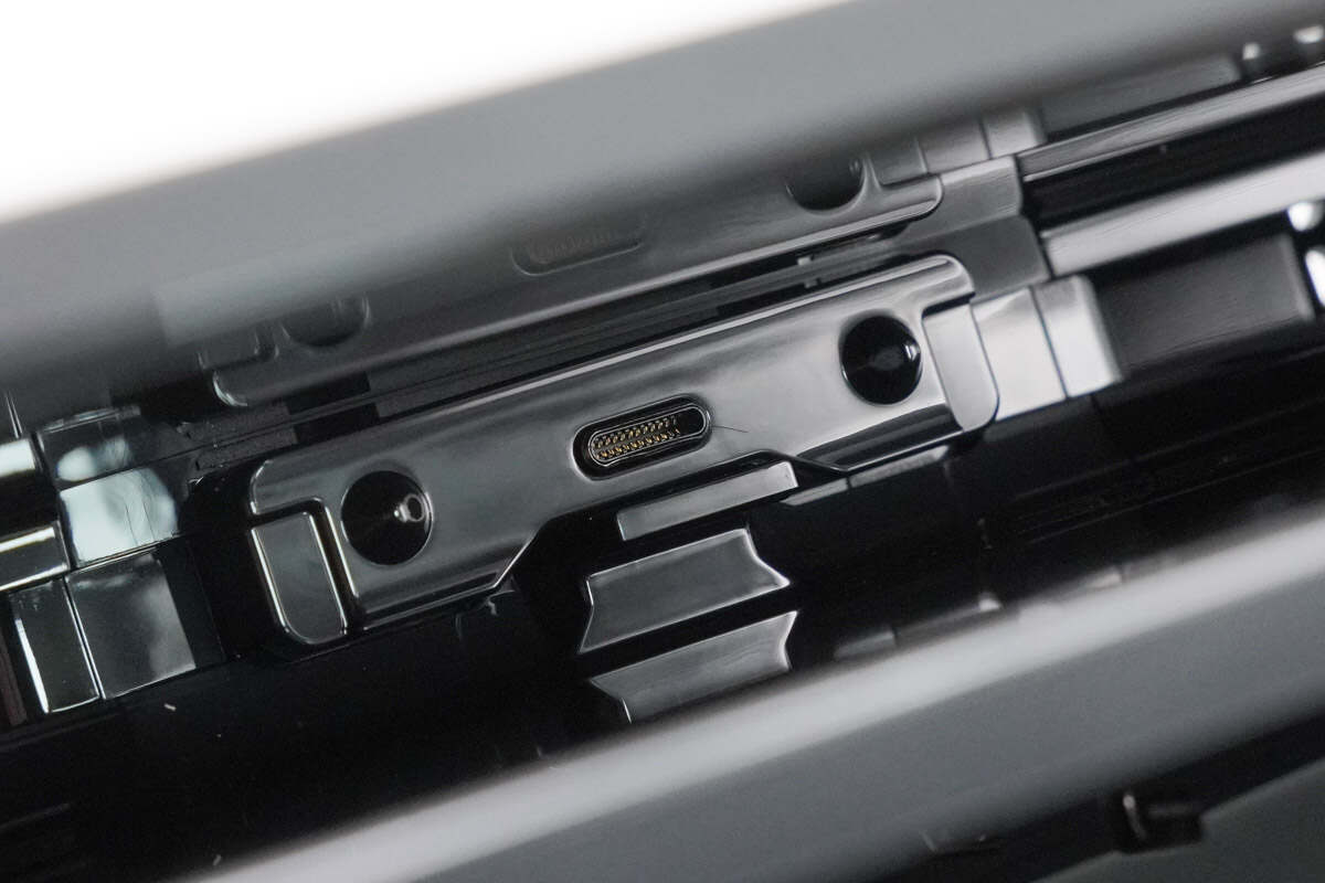
At the center of the slot is a USB-C male connector, with a protective plate held up by an internal spring mechanism.
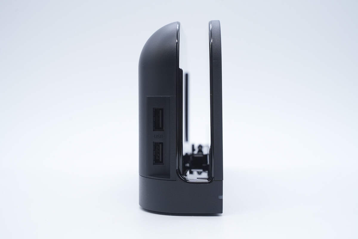
One side of the dock is also equipped with two USB-A ports.
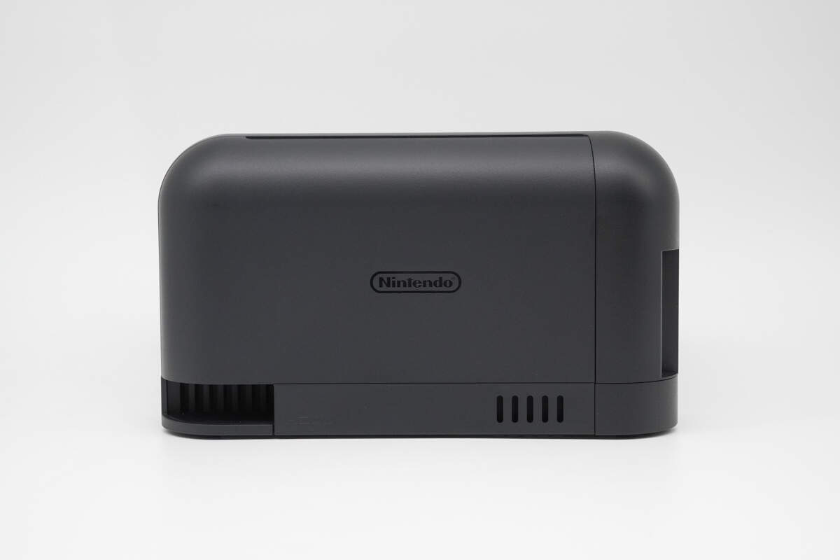
The edges at the back are smoothly rounded, with the Nintendo logo positioned at the center.
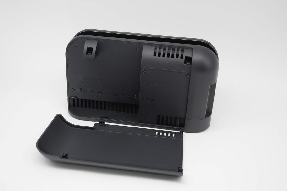
When you open the back cover, the spec information is located on the upper left side.
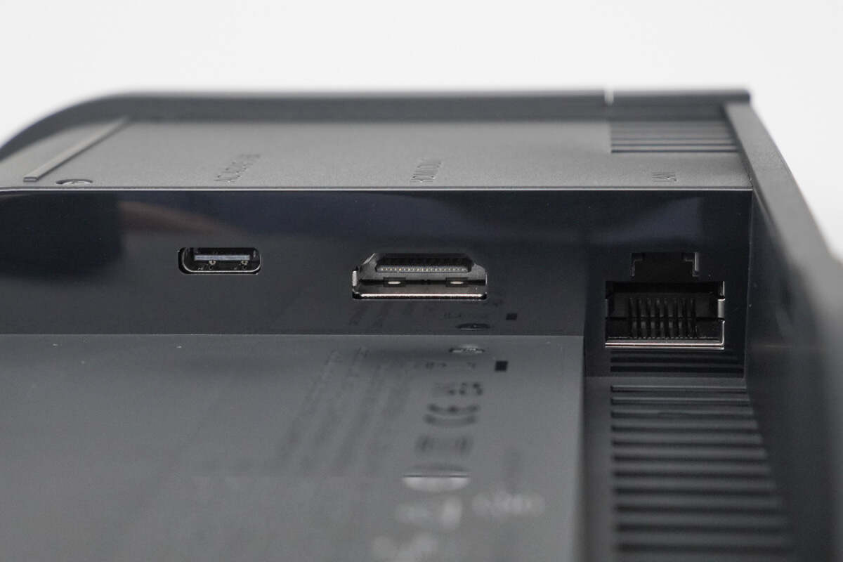
Located here are the USB-C, HDMI, and Ethernet ports.
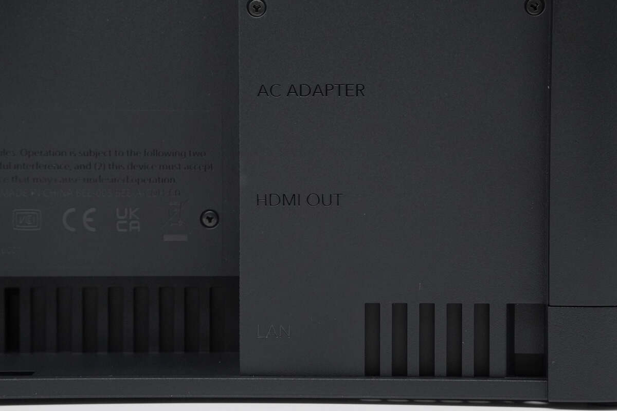
This area displays the labels for AC Adapter, HDMI Out, and LAN ports.
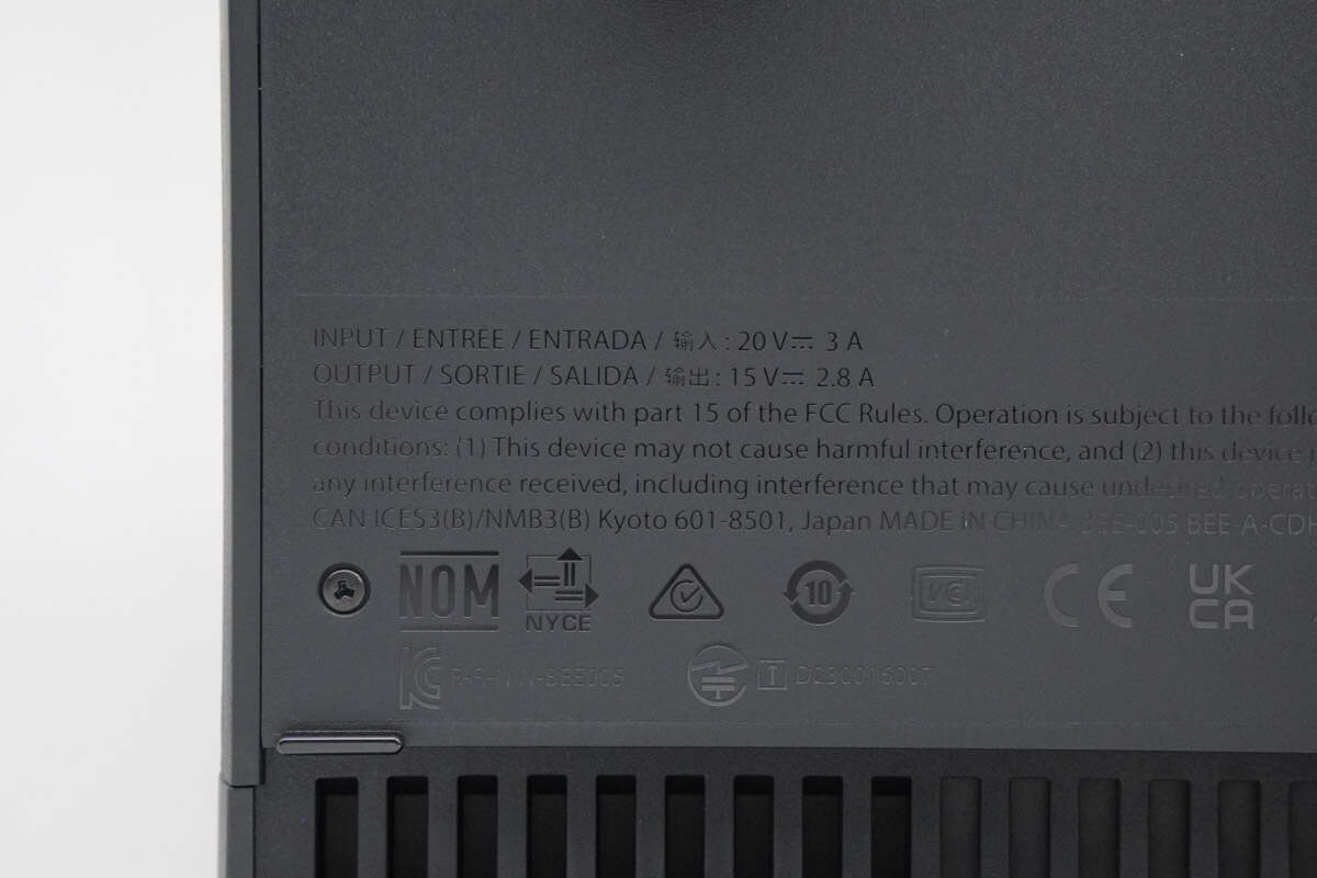
Input: 20V 3A
Output: 15V 2.8A
It is certified by NOM, NYCE, CE, UKCA, KC, and others.
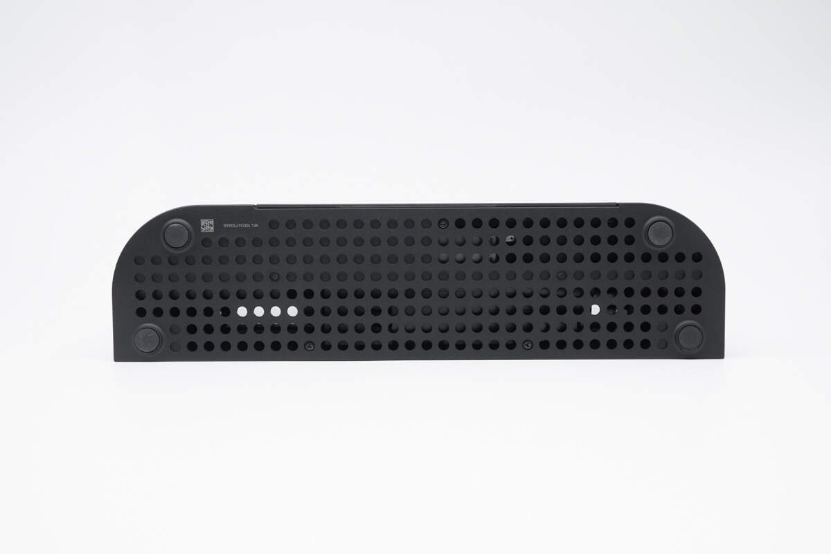
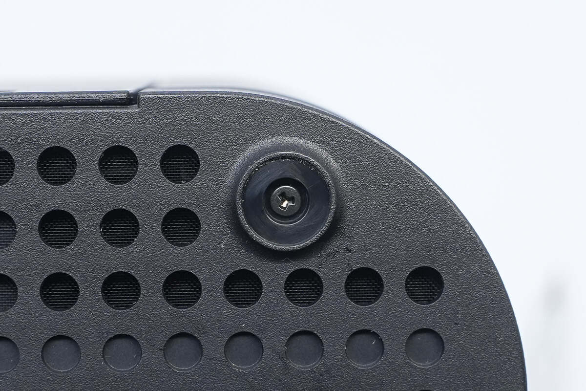
There are anti-slip pads on both sides of the bottom, along with numerous ventilation holes.
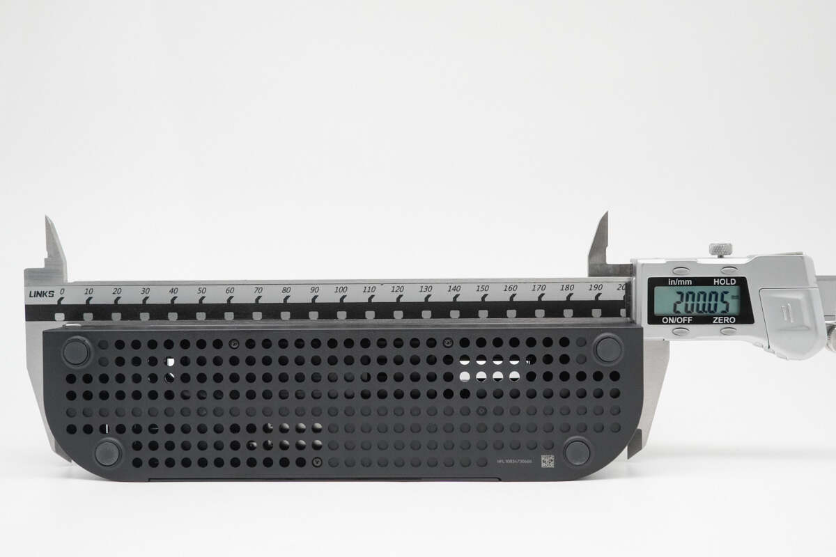
The length is about 200.05 mm (7.88 inches).
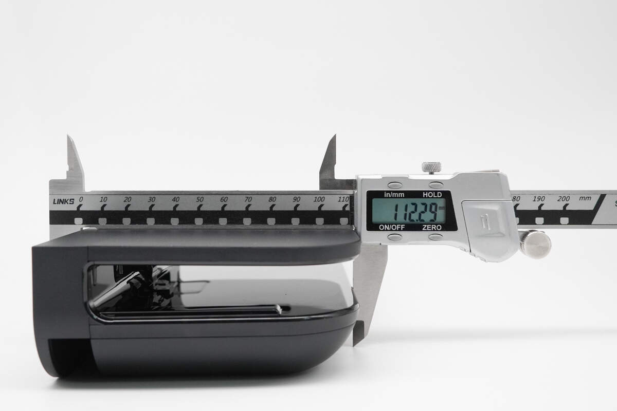
The height is about 112.29 mm (4.42 inches).
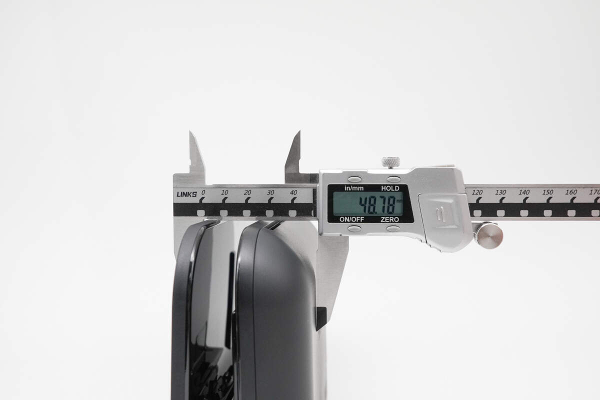
The thickness is about 48.78 mm (1.92 inches).
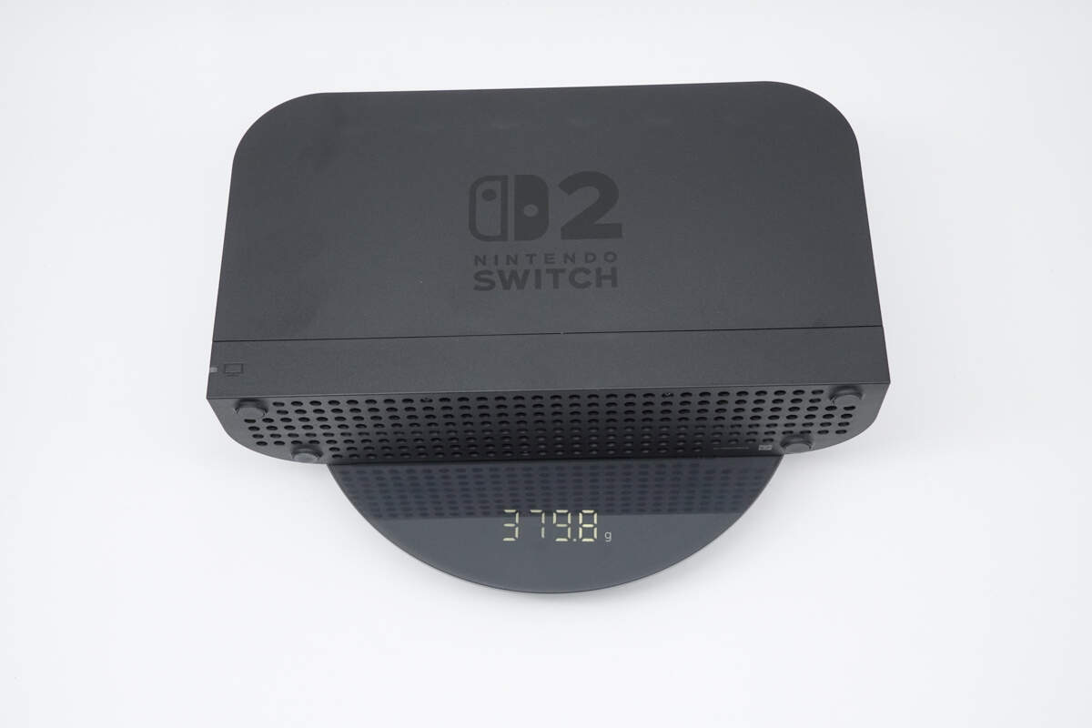
The weight is about 380 g (13.4 oz).
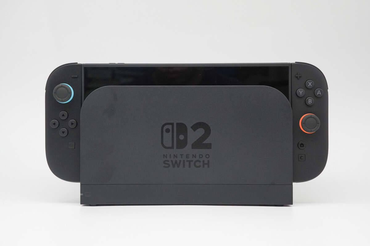
Here’s how the Nintendo Switch 2 looks when placed in the dock.
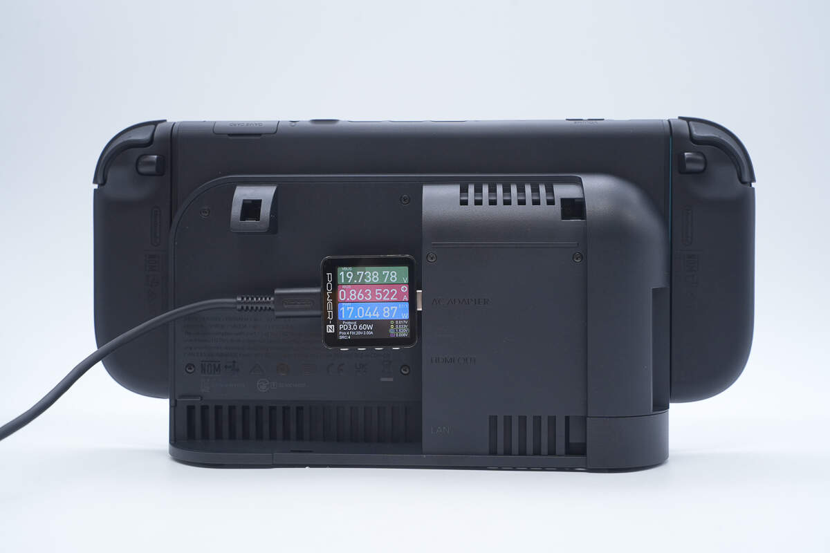
Using the official 60W charger with the dock to charge the Switch 2, the charging power is about 17.04W.
Teardown
Next, let's take it apart to see its internal components and structure.
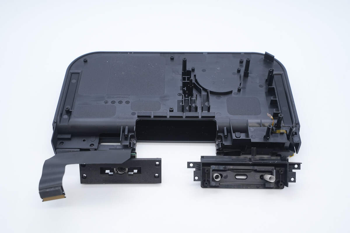
Screws are found under the bottom anti-slip pad.
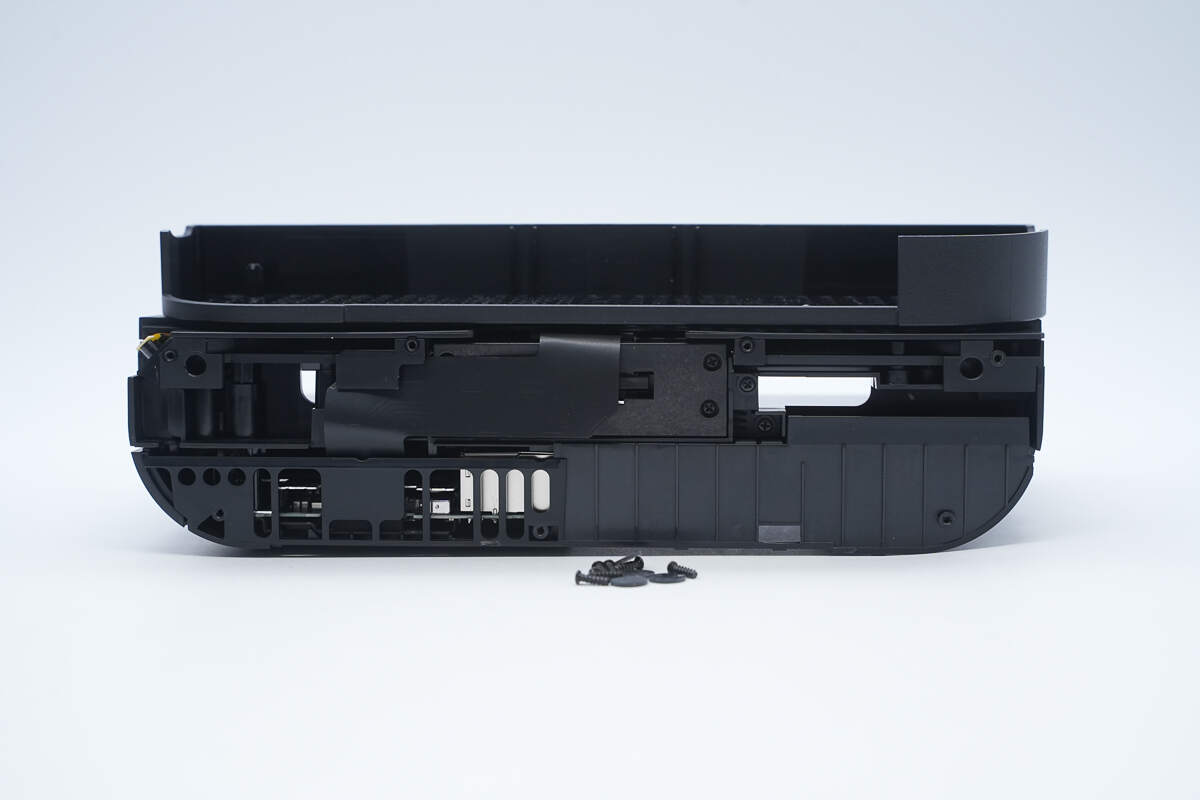
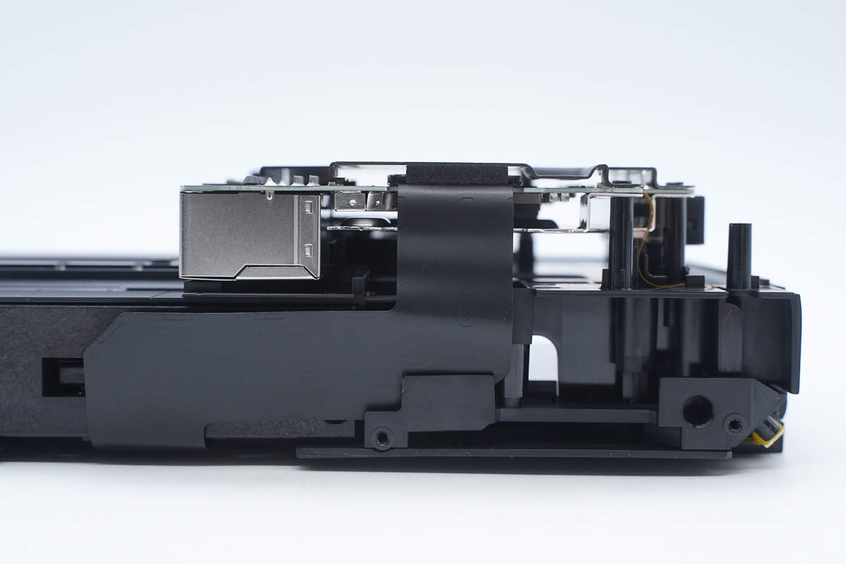
Remove the screws to open the bottom cover. The central USB-C port is a separate module, secured with screws.
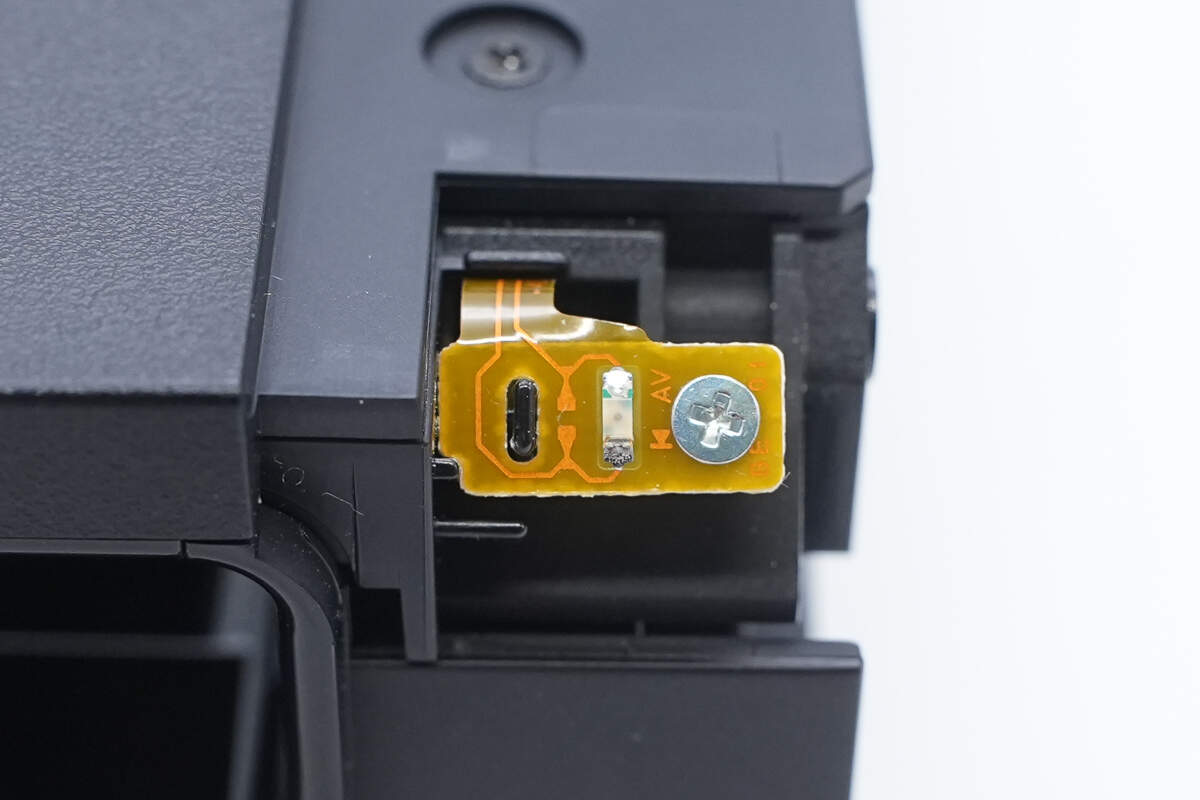
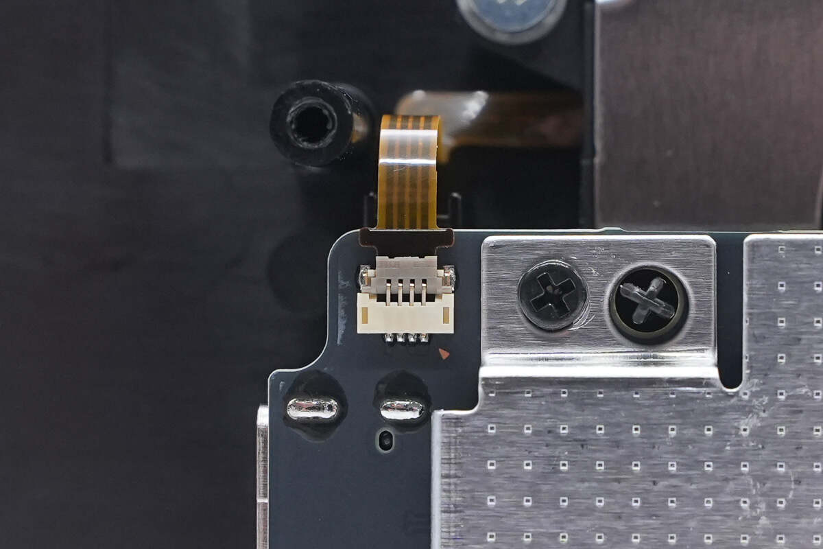
The side LED indicator is soldered to a ribbon cable, which is secured with a screw.
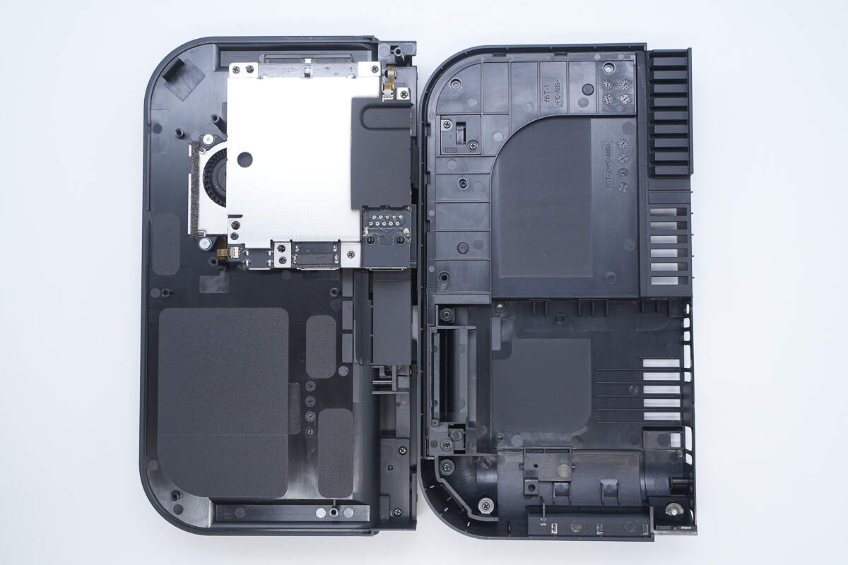
Open the back cover, the casing is made of fire-resistant PC+ABS material.
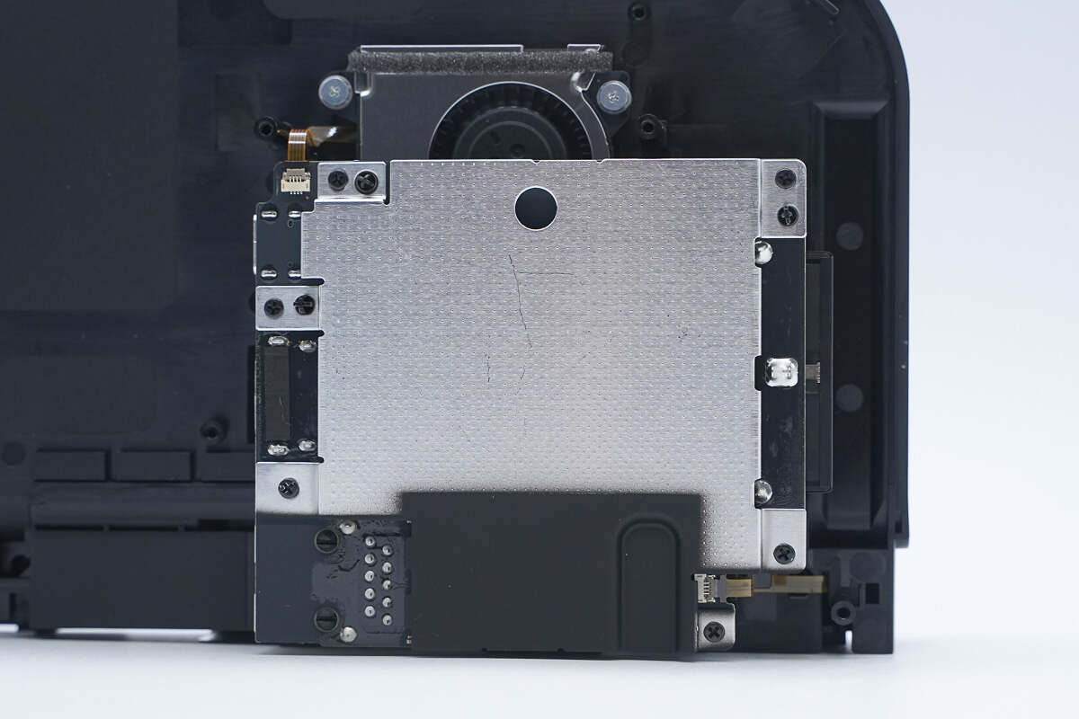
The casing houses the PCBA module and a fan. The PCB is covered with a metal shielding plate and secured with screws.
The PCBA module and fan are connected via a ribbon cable with a plug-and-play design.
The other end of the indicator light’s ribbon cable is also a plug-and-play connector.
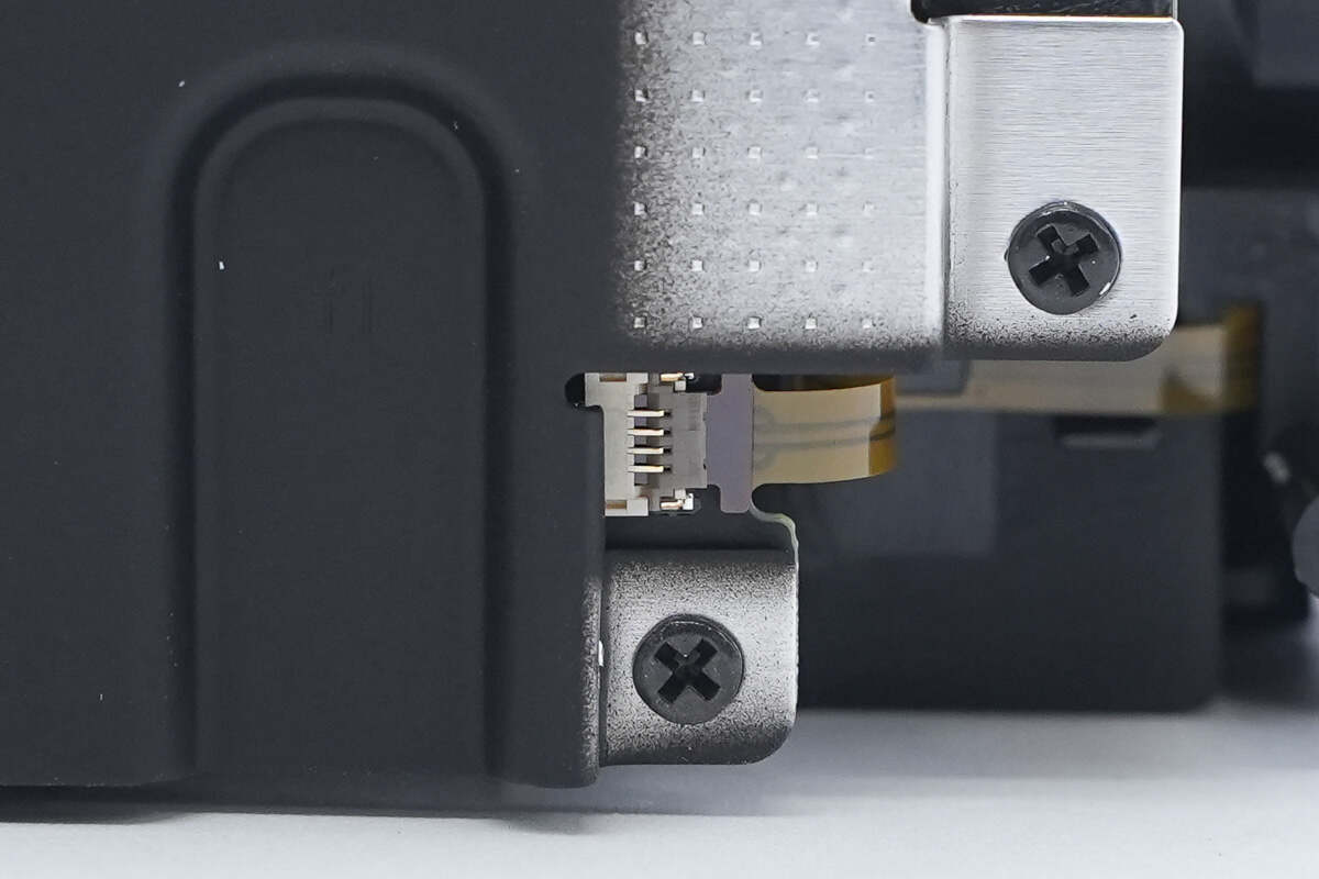
The bottom USB-C is also connected to the PCB via a ribbon cable.
Removing the metal shielding plate reveals that the PCB is also secured by mounting posts, with a reinforcement pad attached to the ribbon cable on the left side.
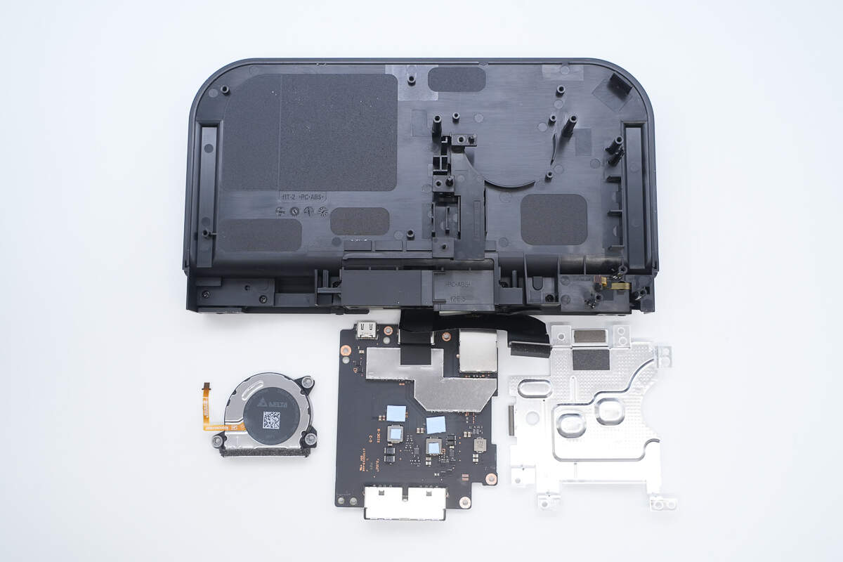
Remove the PCB and fan.
Remove the USB-C output port.
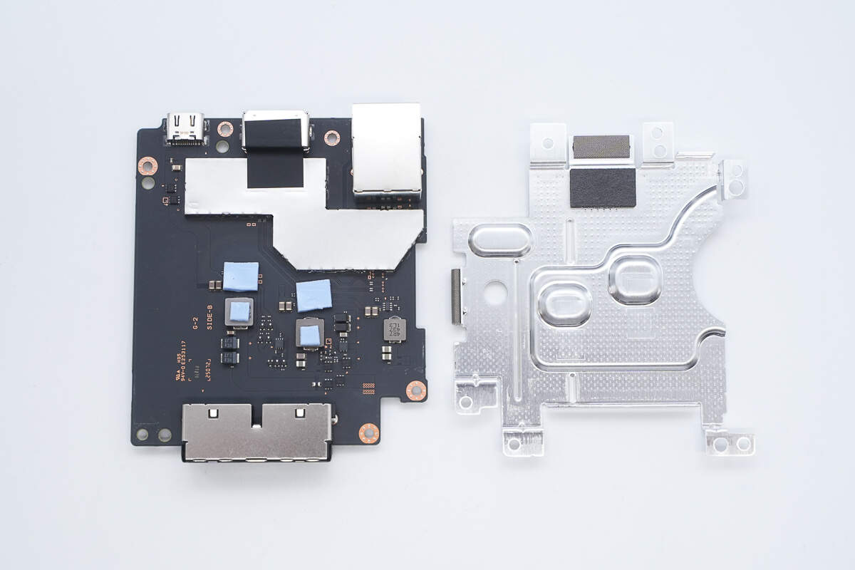
The back of the PCBA module is equipped with a metal heat sink.
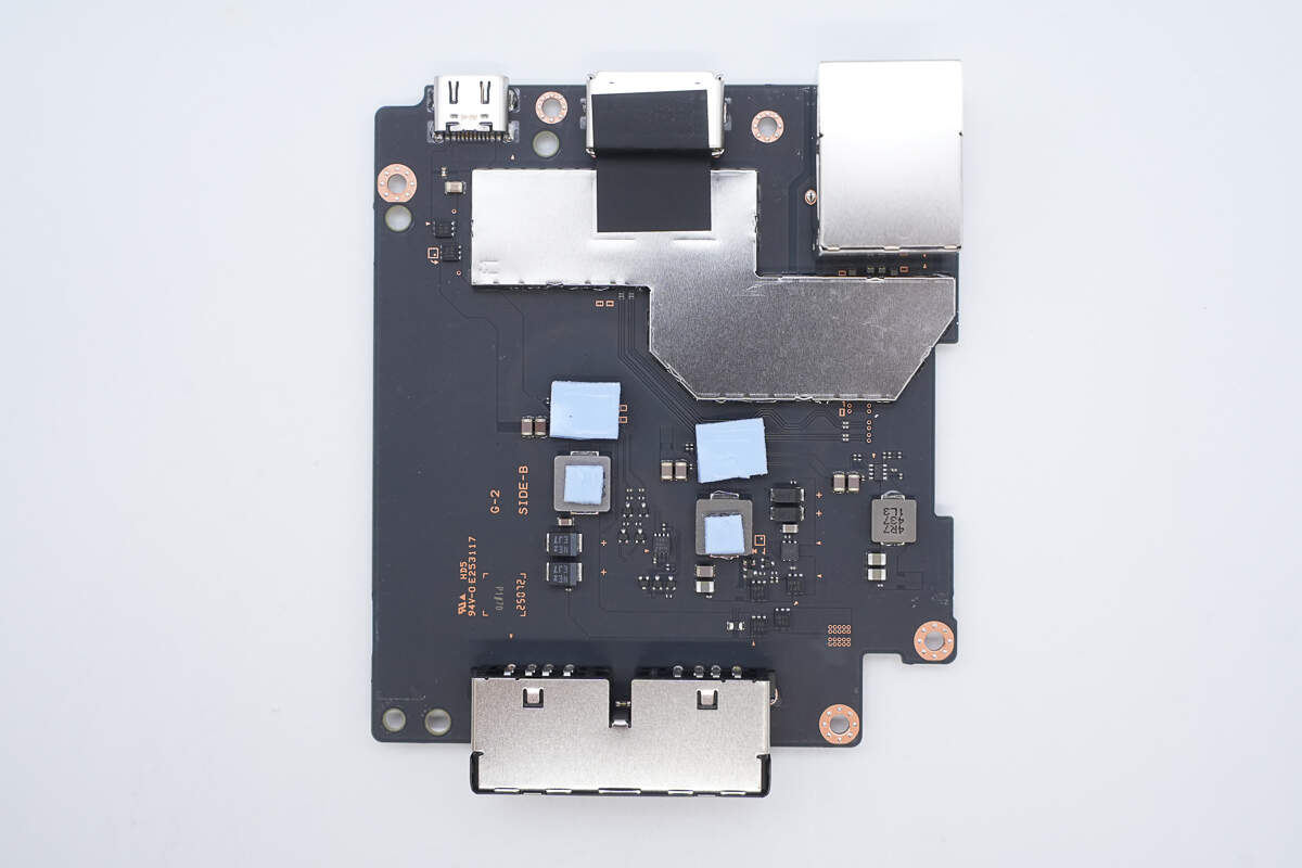
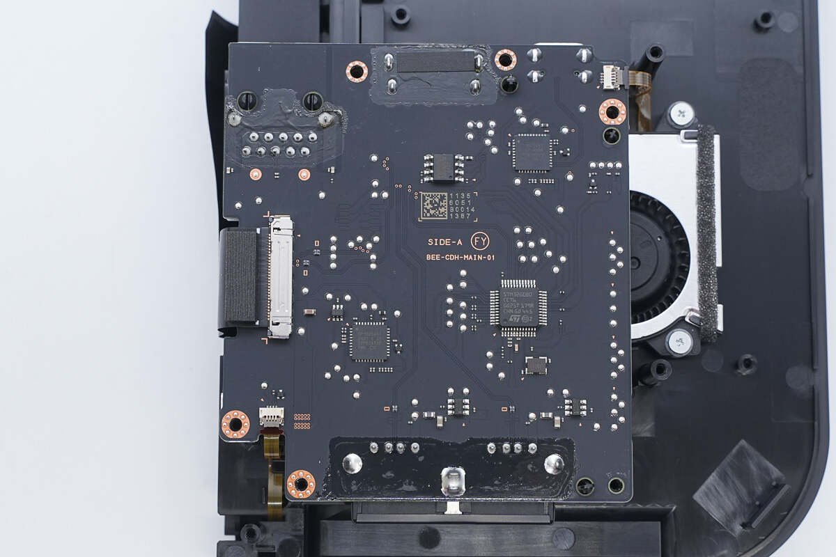
USB-C, HDMI, RJ45, and USB-A connectors are soldered on both sides of the PCB, with a shielding cover over the hub circuitry area.
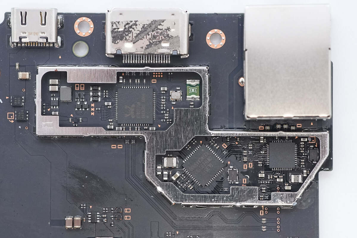
Opening the shield reveals components such as the hub controller, video converter chip, and Ethernet controller.
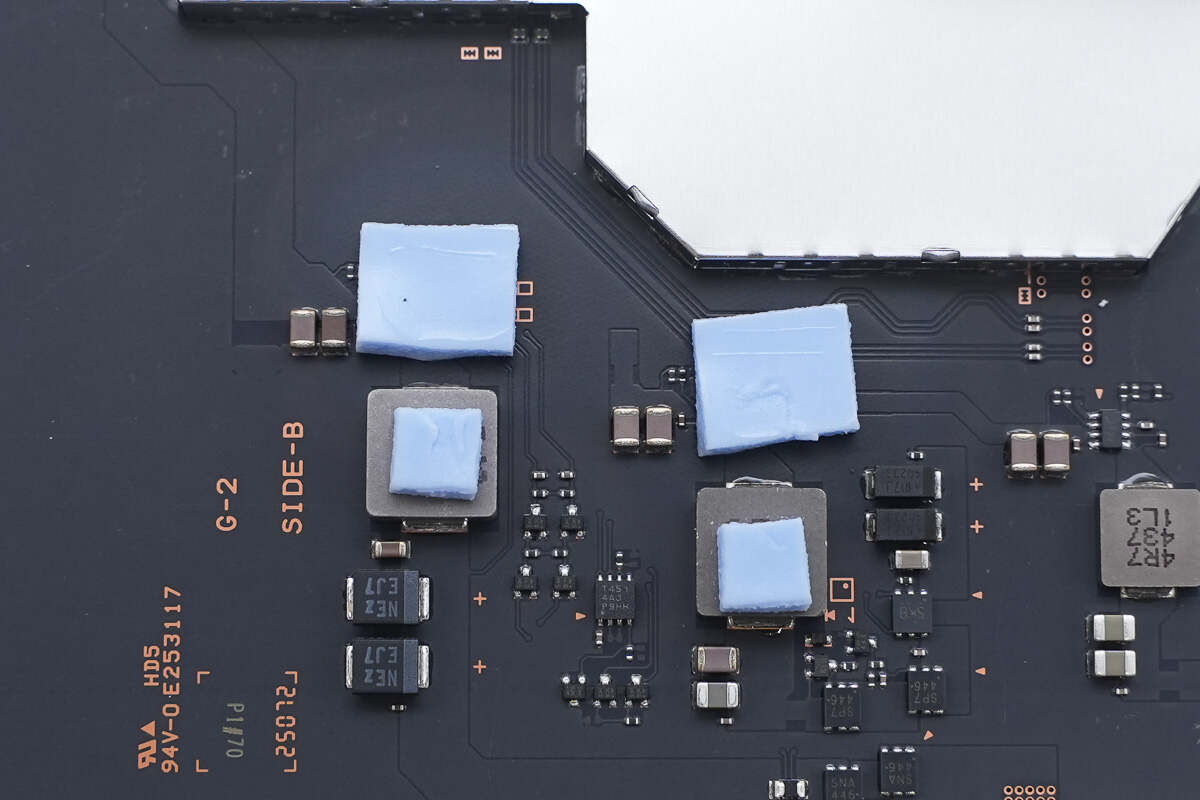
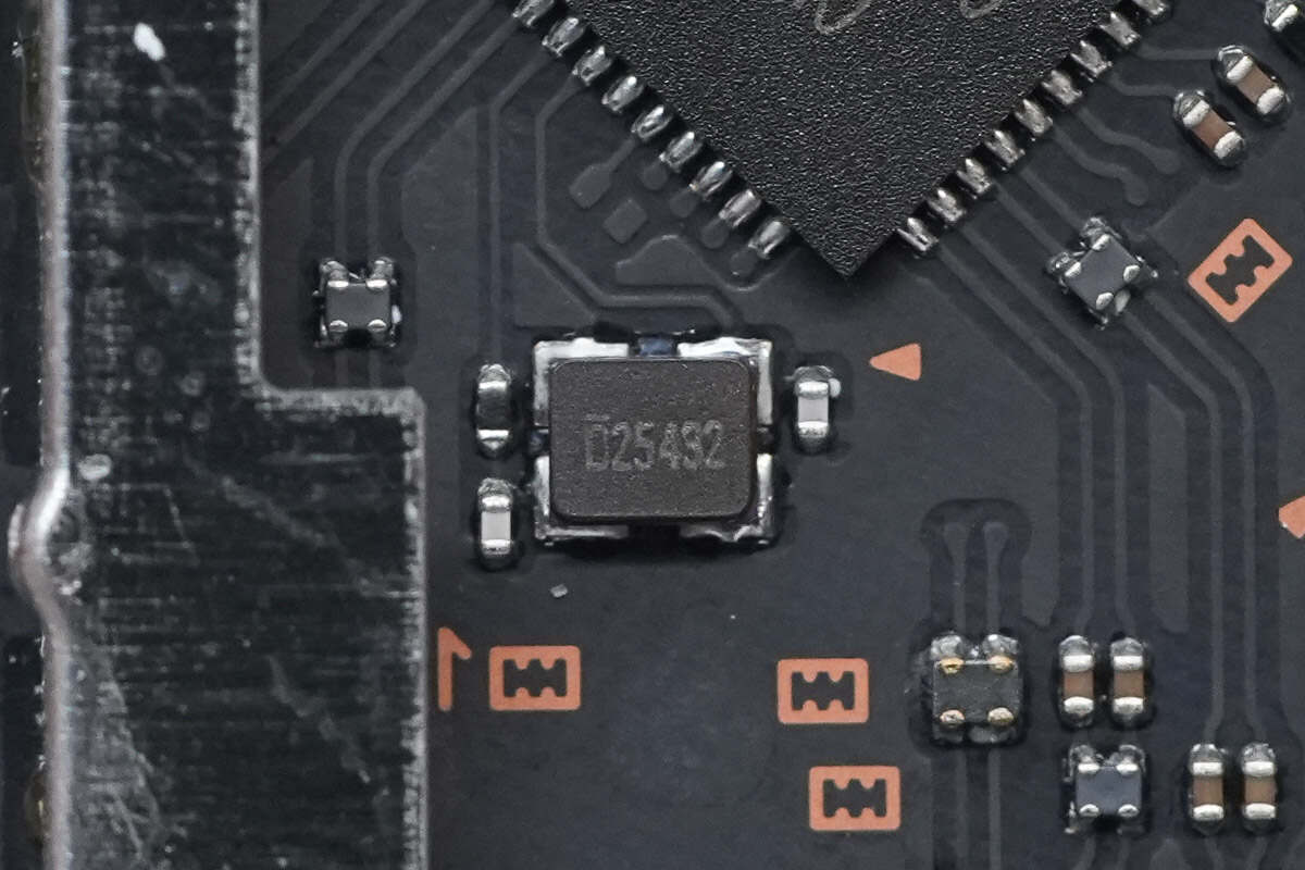
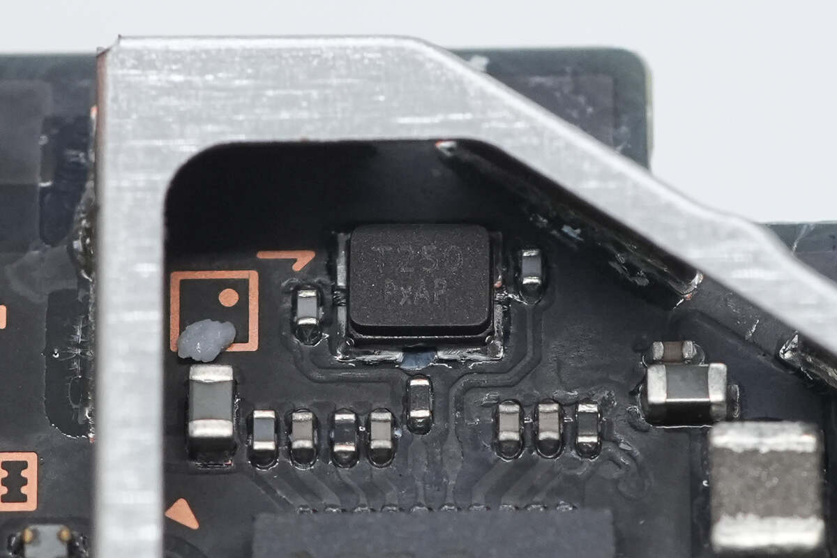
Thermal pads are attached to the synchronous buck converter and buck inductor used for step-down output to the USB-A ports.
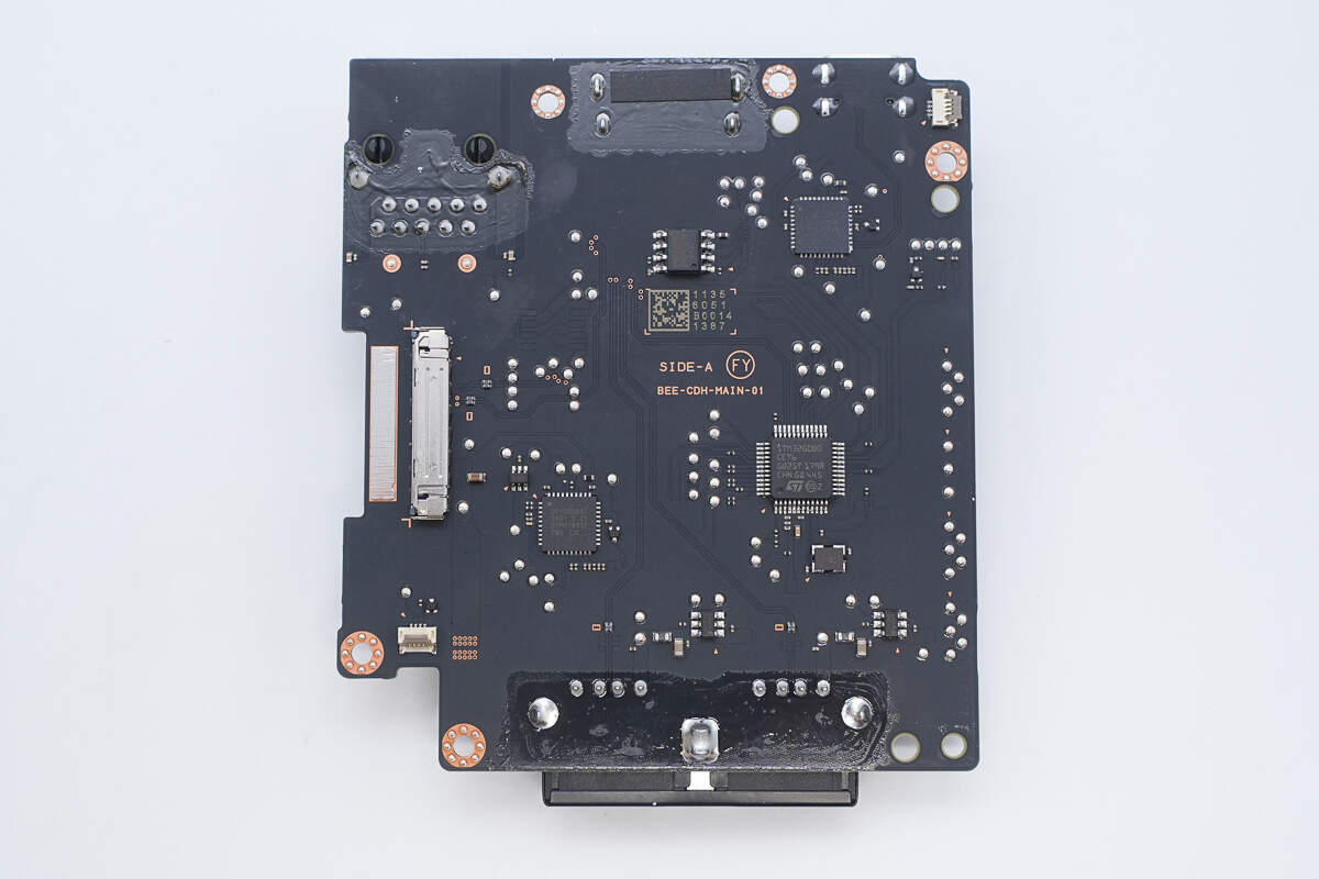
On the back, there are components including an MCU, two USB-C port controllers, and a memory chip.
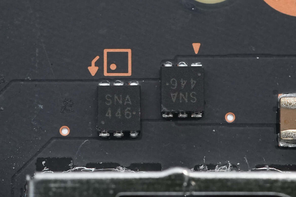
For power control of the USB-C input port, there are two back-to-back MOSFETs marked with "SNA".
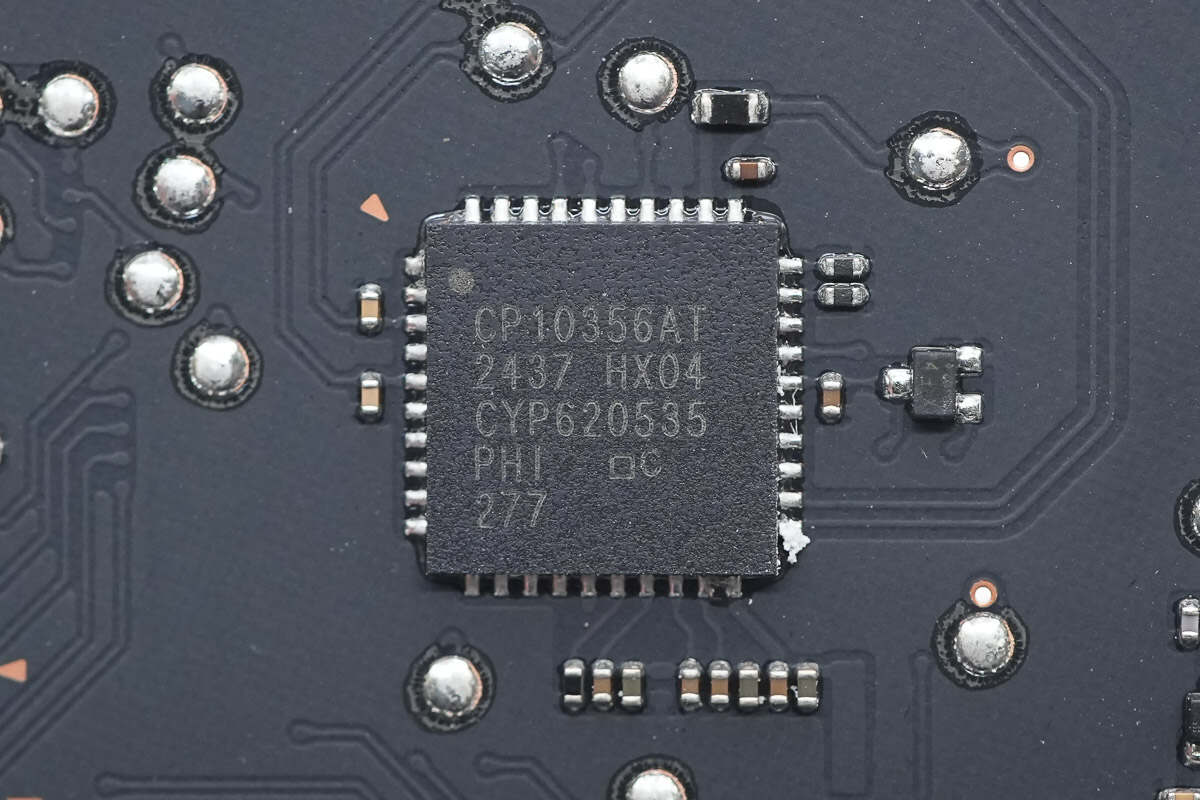
The USB-C input port controller is from Infineon, marked with CP10356AT, and uses a QFN40 package.
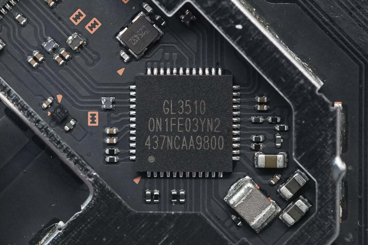
The USB hub controller is the GL3510 from Genesys, a four-port, low-power hub controller that supports USB 3.0 and is backward compatible with USB 2.0. It features a built-in switching regulator for power supply. In this design, the GL3510 is used for USB 3.0 expansion, connecting three USB-A ports and cascading to another GL3510.
Close-up of the external crystal oscillator for the hub controller.
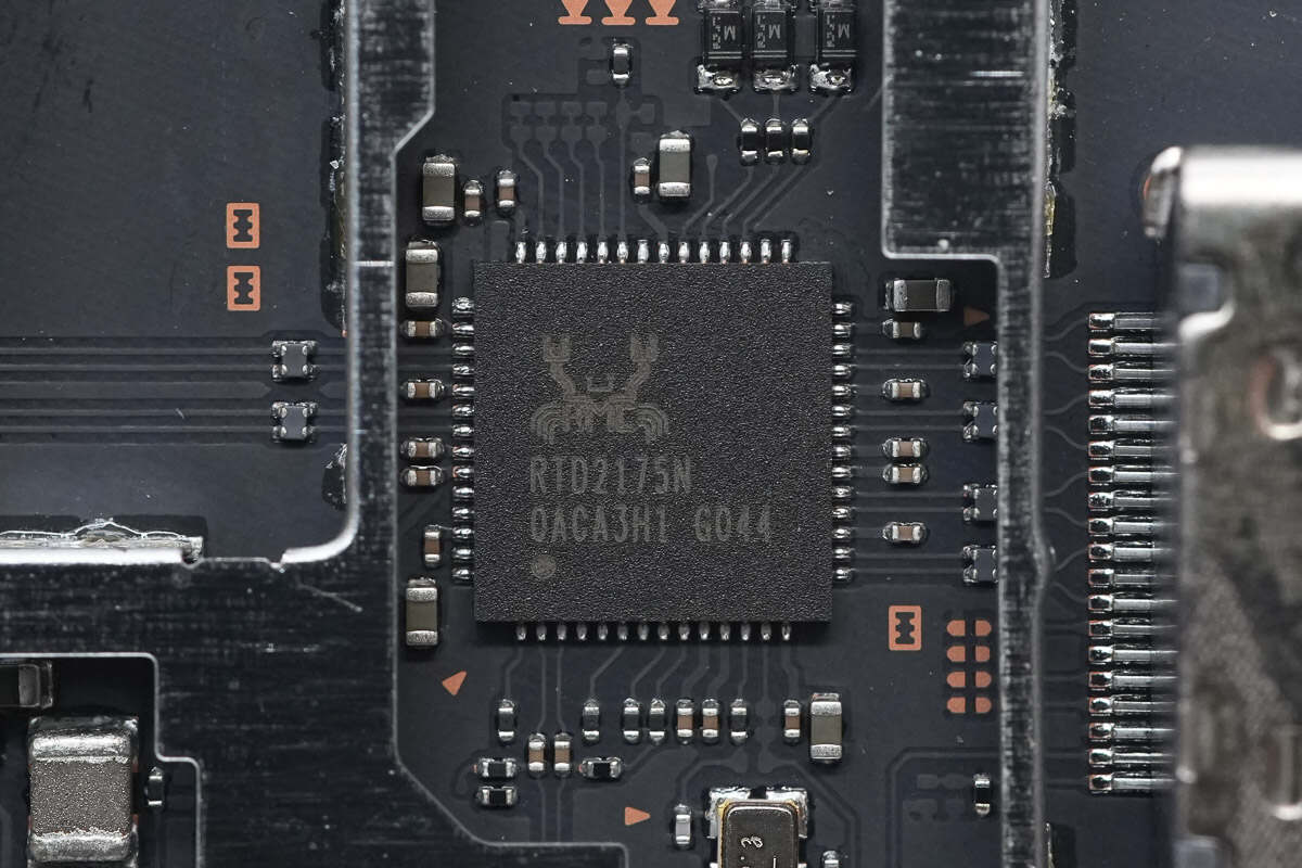
The video converter chip is from REALTEK, model RTD2175N, which is a DP-to-HDMI conversion chip.
Close-up of the external crystal oscillator.
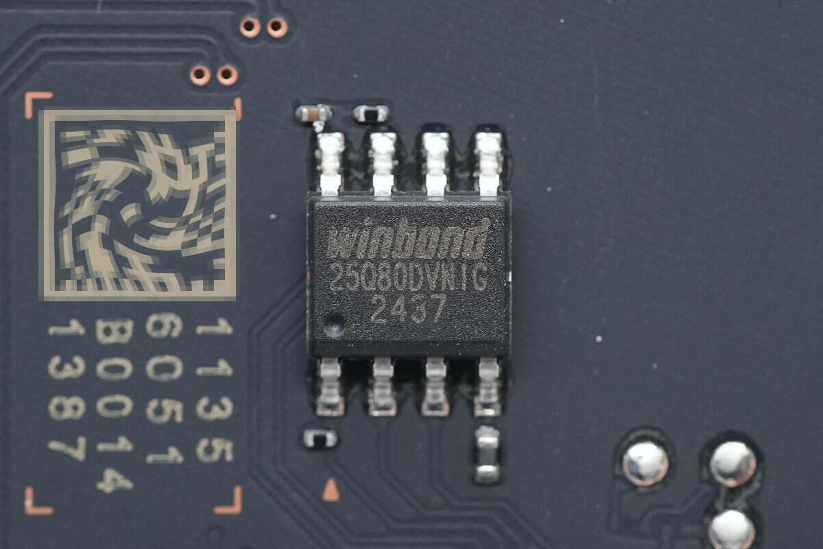
The memory chip is from Winbond, model W25Q80DV. It is a serial NOR flash memory that operates on a single 2.7–3.6V power supply, with standby power consumption as low as 1µA. The entire series comes in compact packages.
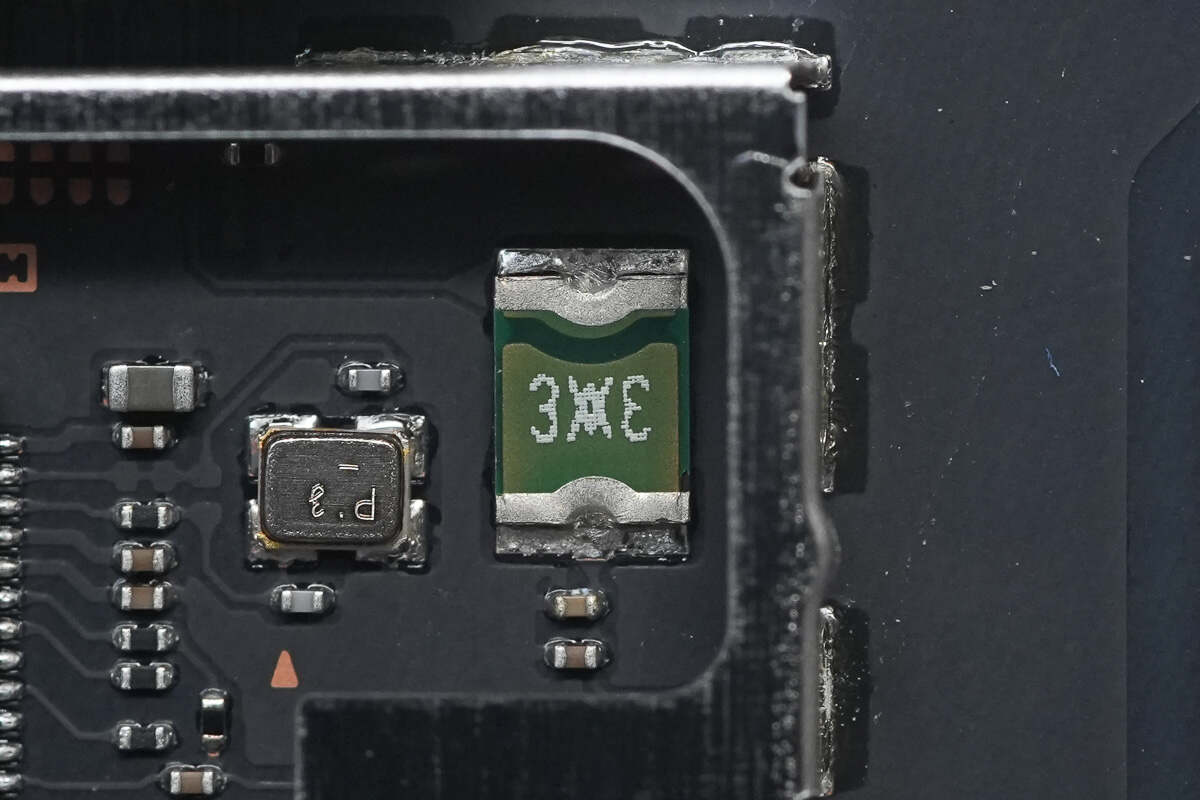
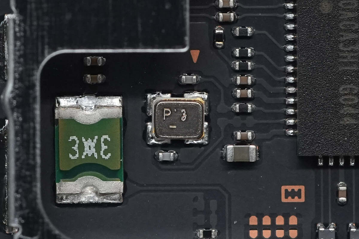
Close-up of a self-resetting fuse.
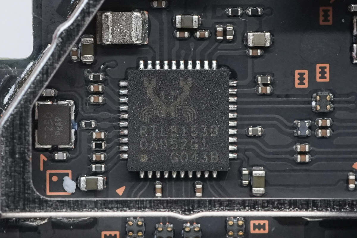
The Ethernet controller is from REALTEK, model RTL8153B. It supports gigabit transfer speeds and comes in a QFN40 package.
Close-up of the external crystal oscillator for the Ethernet controller.
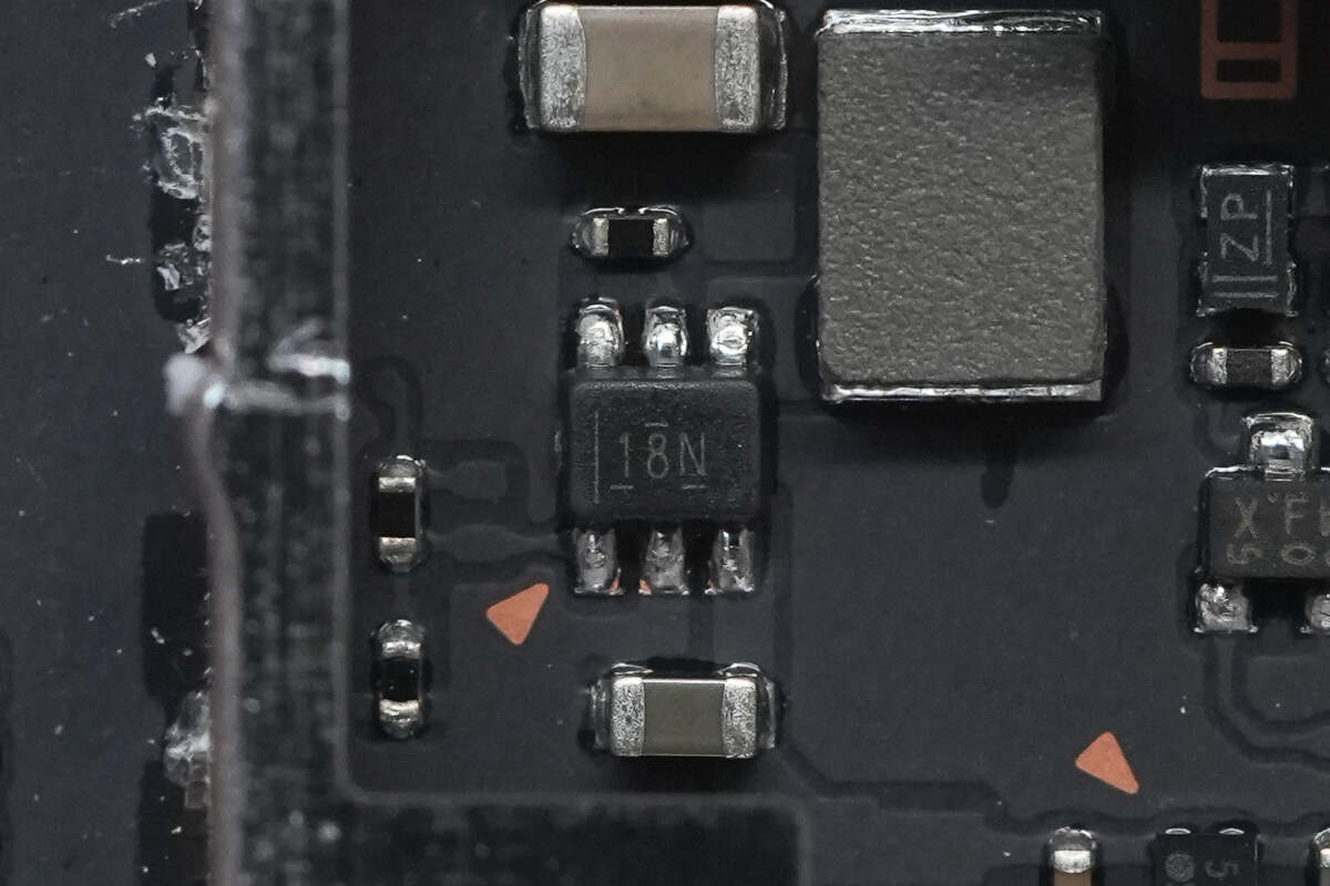
The buck chip is from TI, marked with 18N, model TLV62568. It is a synchronous buck converter with a 5.5V input, 1A output current, and comes in a SOT563 package.
Close-up of the accompanying SMD buck inductor.
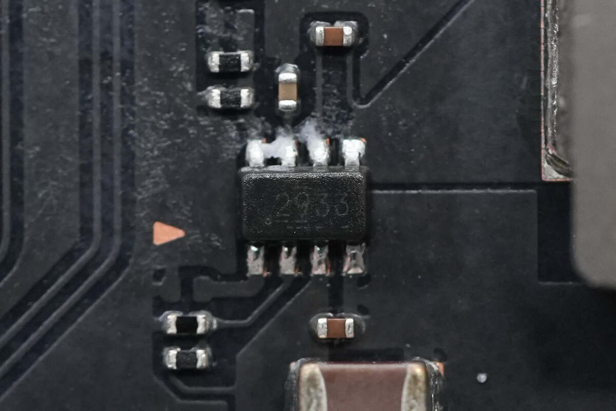
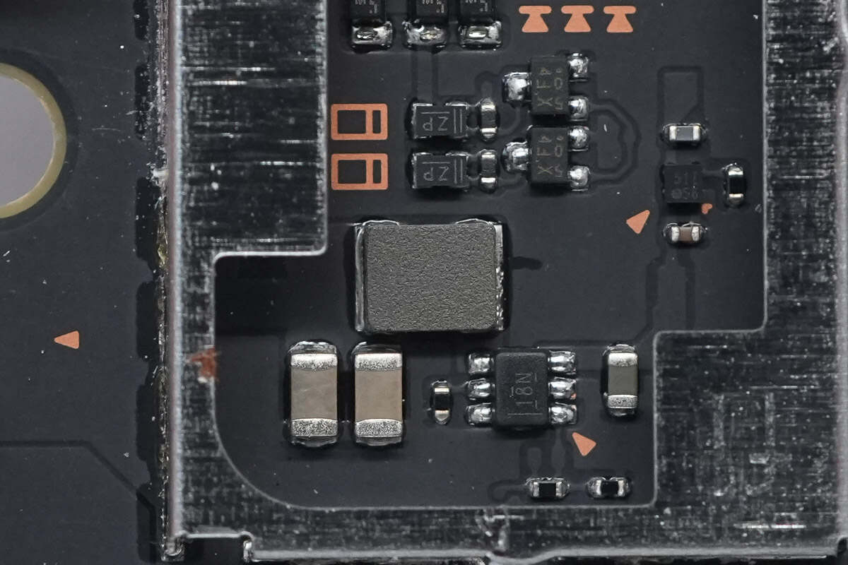
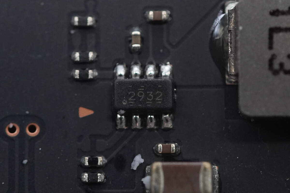
The synchronous buck chips used for the two step-down circuits powering the USB-A ports are both from TI, marked with 2933, model TPS62933. They support a 30V input voltage and 3A output current. The chips integrate MOSFETs internally, support up to 22V output voltage, and come in SOT583 packages.
Close-up of the accompanying 3.9μH buck inductor.
Close-up of the tantalum capacitor used for buck output filtering.
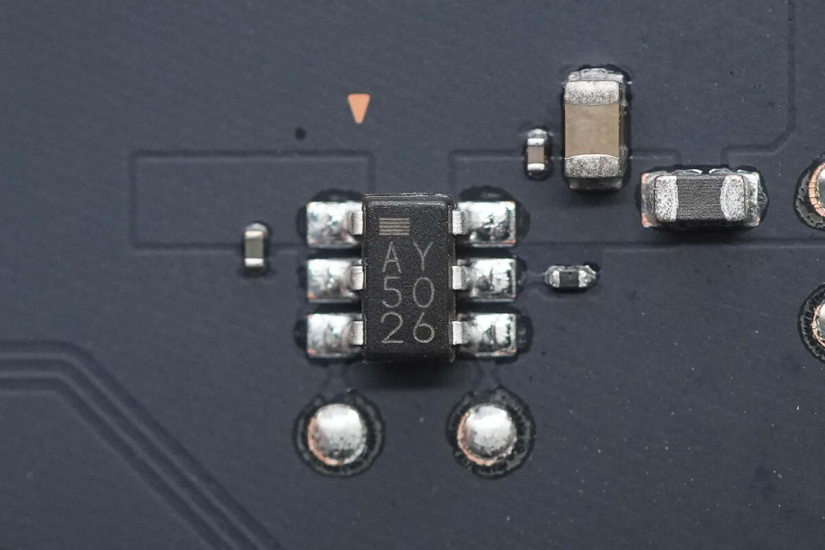
The USB-A port current-limiting chip is from ROHM, marked AY, model BD2242G. It features a built-in low-resistance MOSFET, adjustable current limit from 0.2 to 1.7A, supports output discharge, and comes in an SSOP6 package.

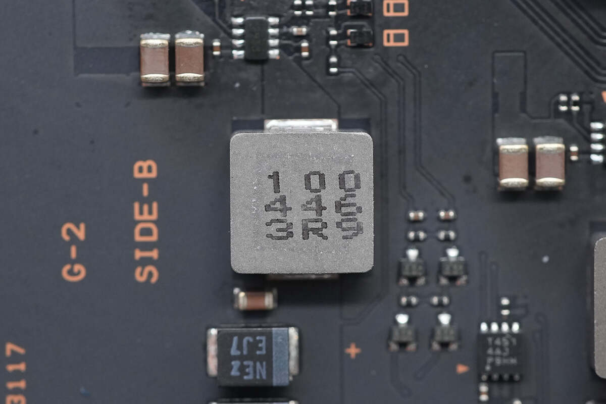
Close-up of the other TI TPS62933 synchronous buck converter.
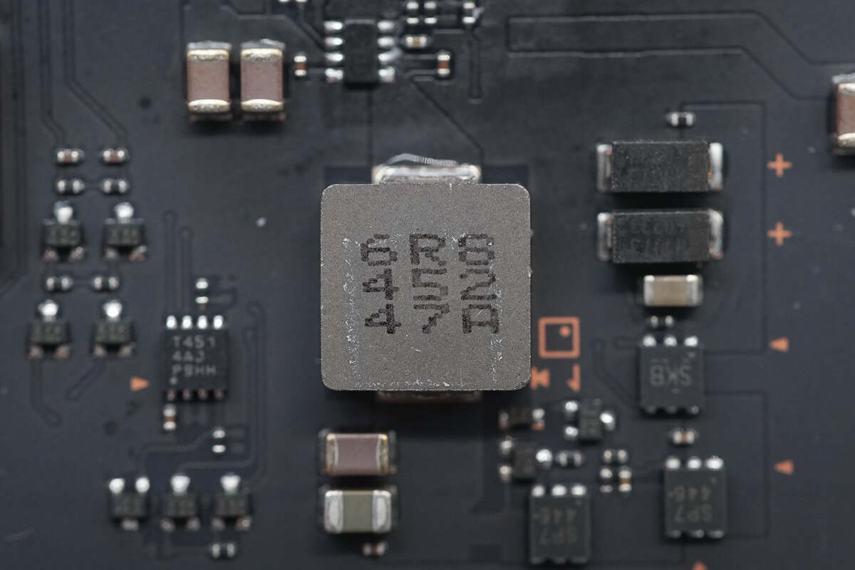
Close-up of the accompanying 6.8μH buck inductor.
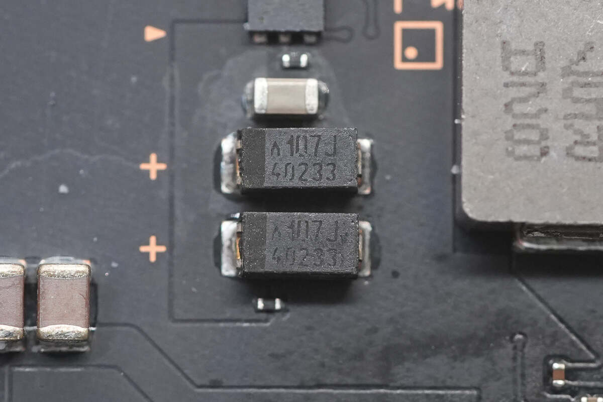
The two tantalum capacitors are rated at 100μF, 6V.
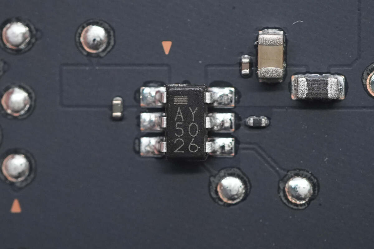
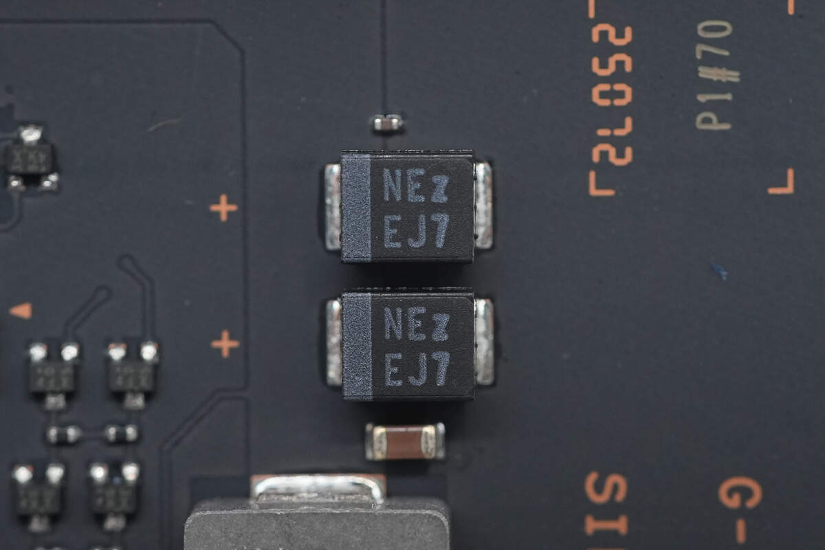
The other USB-A port also uses the ROHM BD2242G overcurrent protection chip.
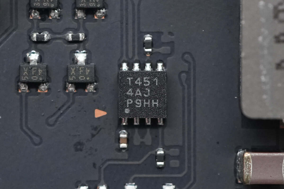
A temperature sensor is used in the two buck circuits, from TI, marked T451, model TMP451. It supports external sensing and comes in a WSON8 package.
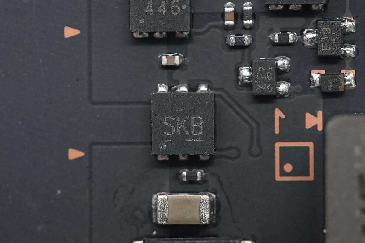
The load switch is from TI, marked with SKB, model TPS25200. It is an eFuse that supports reverse current blocking, with an operating voltage of 6.5V and a current rating of 2.9A. It comes in a WSON6 package.
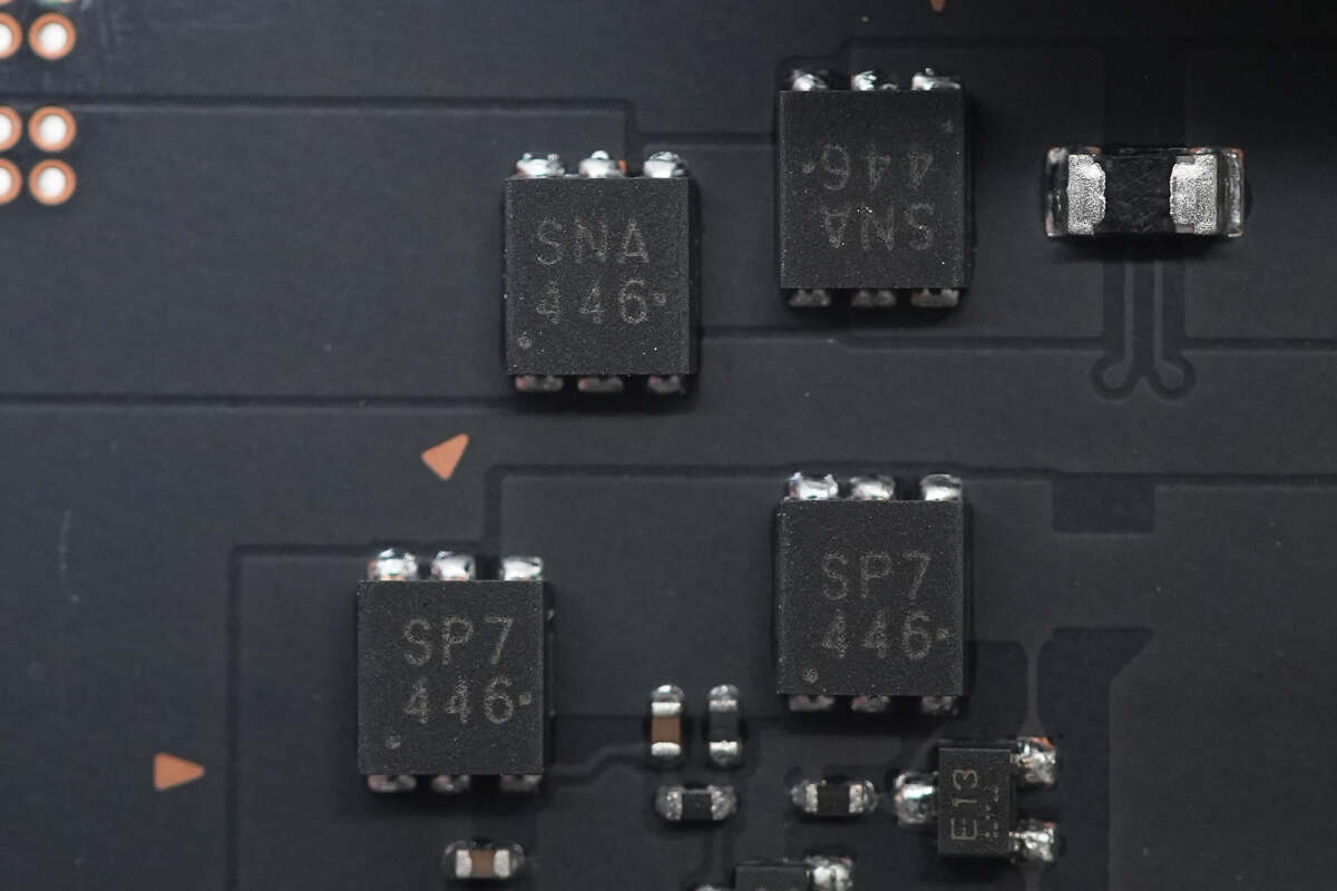
The VBUS MOSFETs marked with SNA and SP7 are used for power switching.
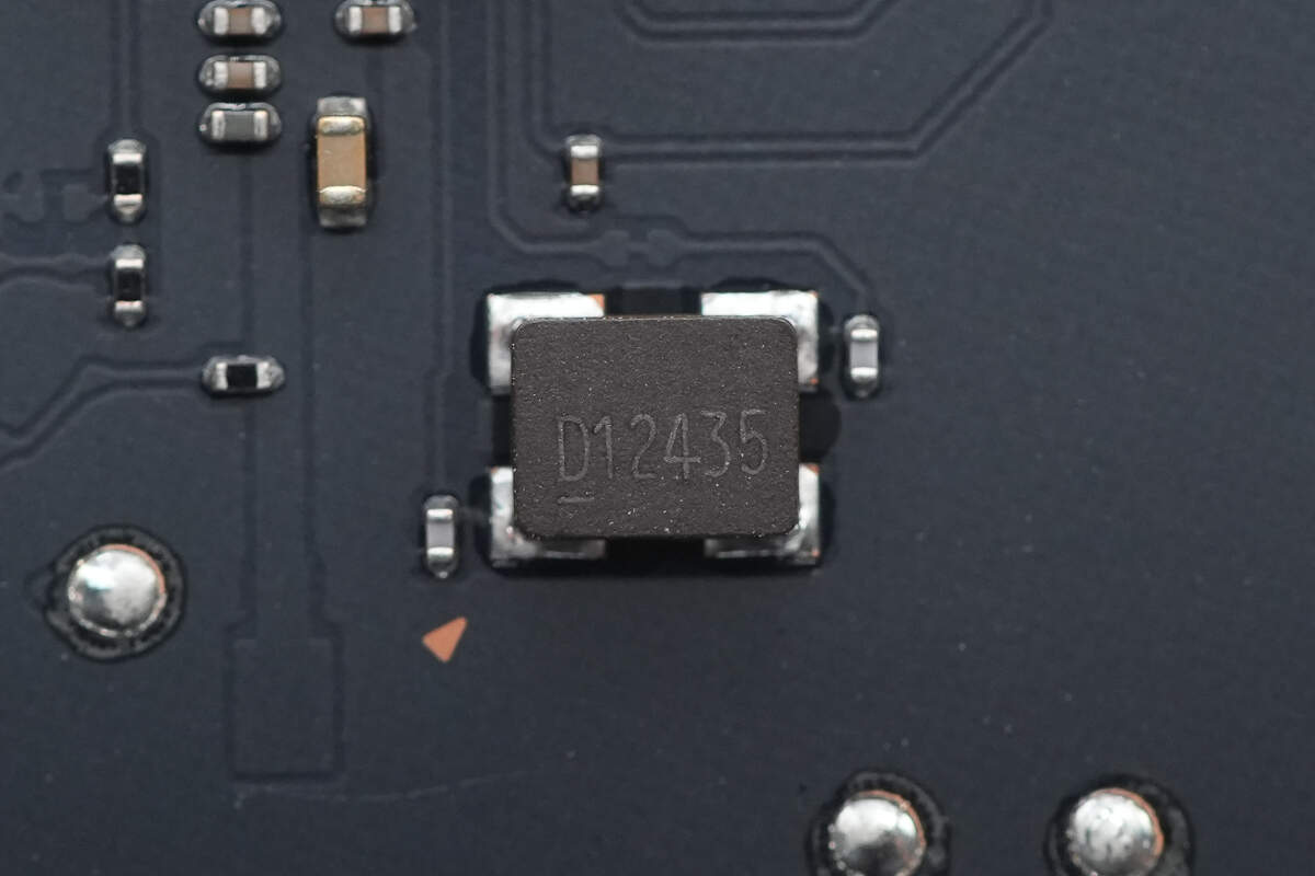
The synchronous buck converter used for the USB-C output port is the TI TPS62932. It integrates internal switching transistors and supports a wide input voltage range of 3.8–30V, with an output voltage range of 0.8–22V. It delivers a continuous output current of 2A and comes in a SOT583 package.
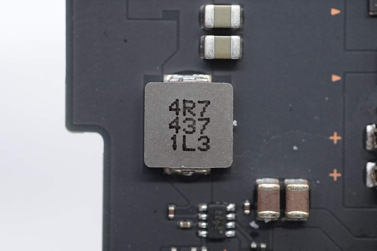
Close-up of the accompanying 4.7μH buck inductor.
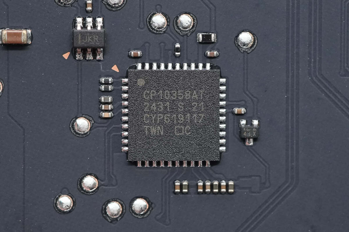
The USB-C output port controller is also from Infineon, marked CP10358AT, and comes in a QFN40 package.
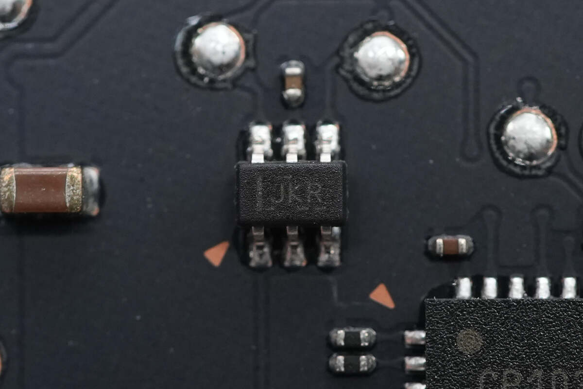
The analog switch is from TI, marked JKR, model TPS5A3160. It is a single-pole double-throw (SPDT) analog switch and comes in an SC70 package.
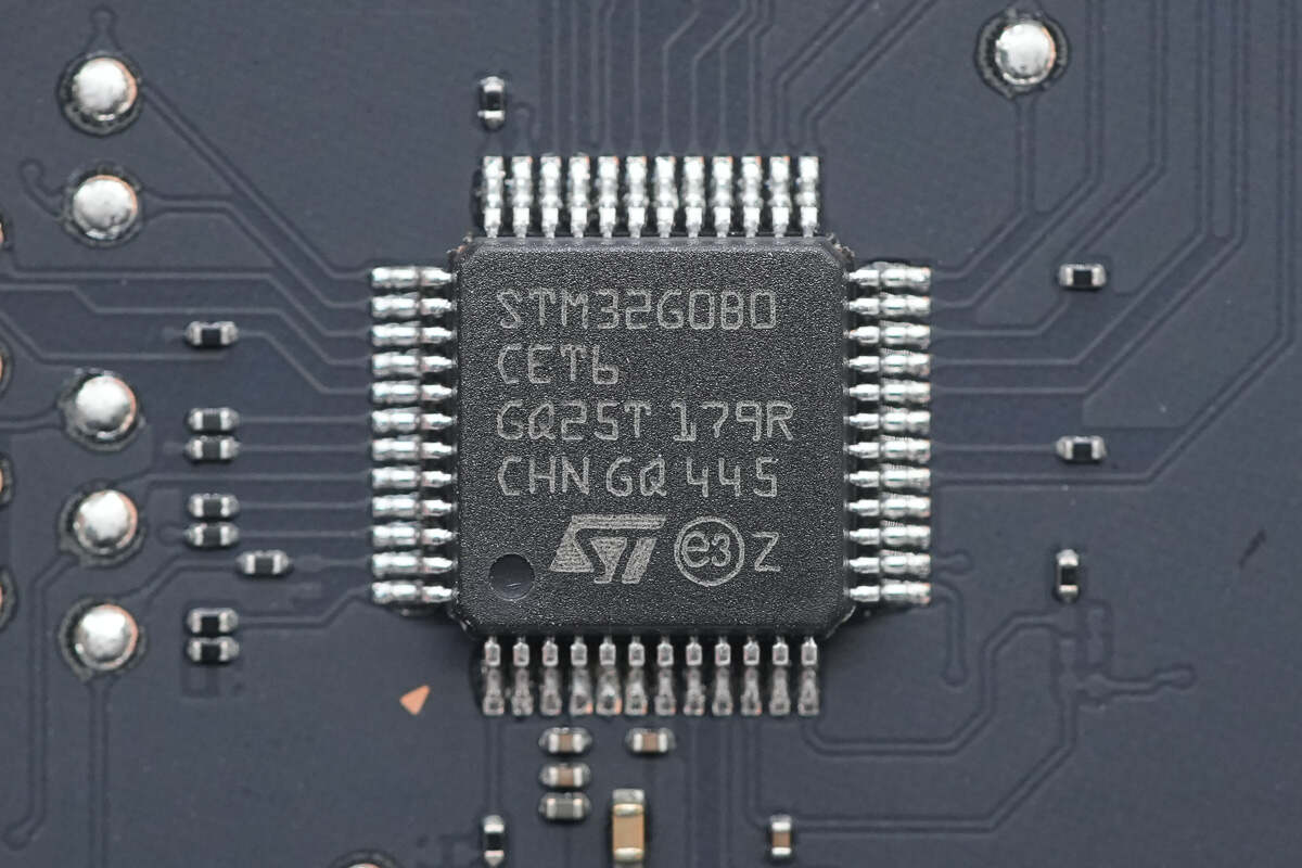
The MCU for overall control is from STMicroelectronics, model STM32G0B0CET6. It features an ARM Cortex-M0+ core, 512KB Flash, and 144KB RAM, housed in an LQFP48 package.
Close-up of the external crystal oscillator for the MCU.
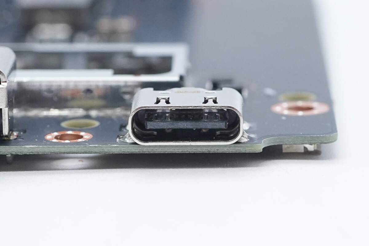
The USB-C input socket is soldered using through-hole technology.
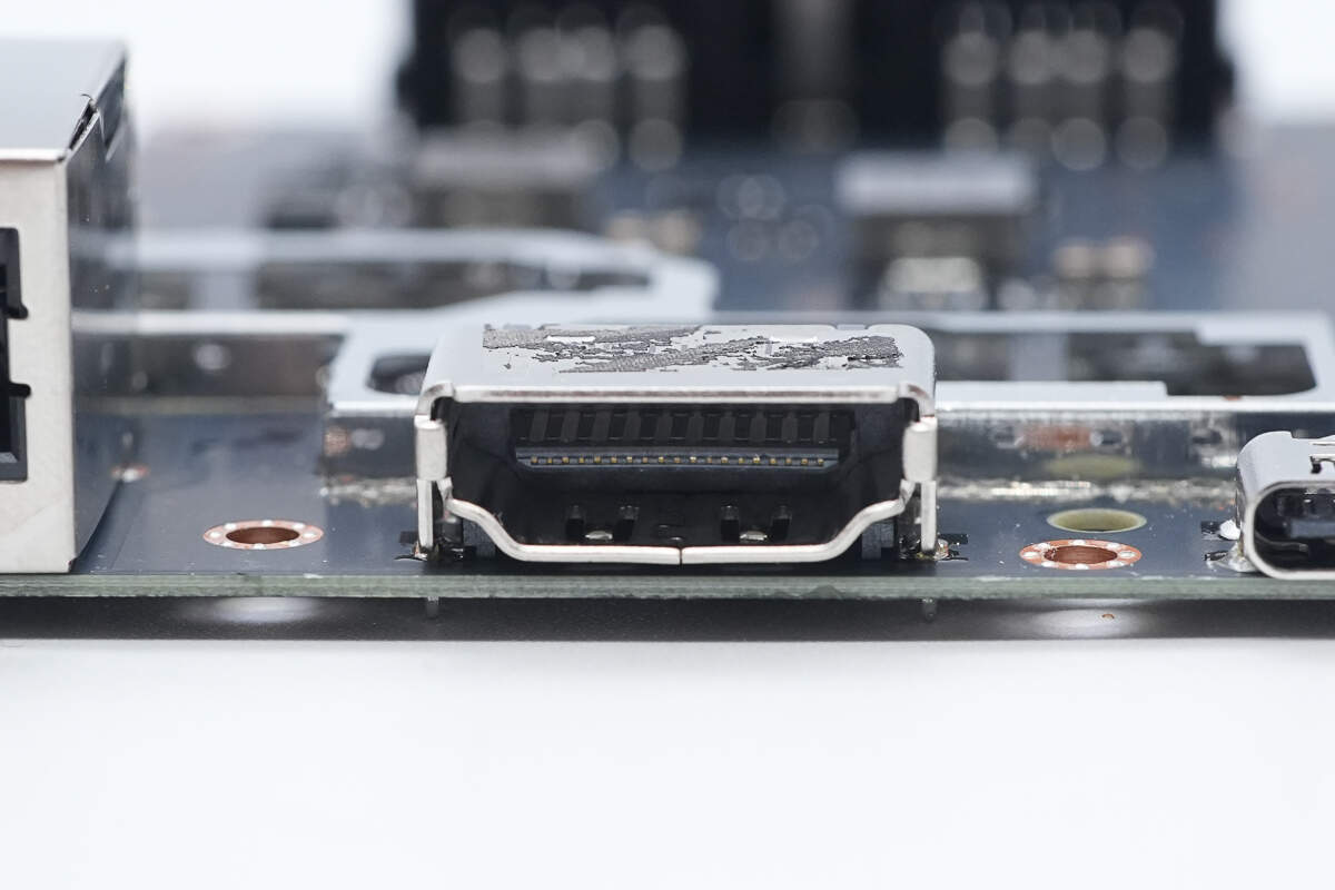
The HDMI socket is also soldered using through-hole technology.
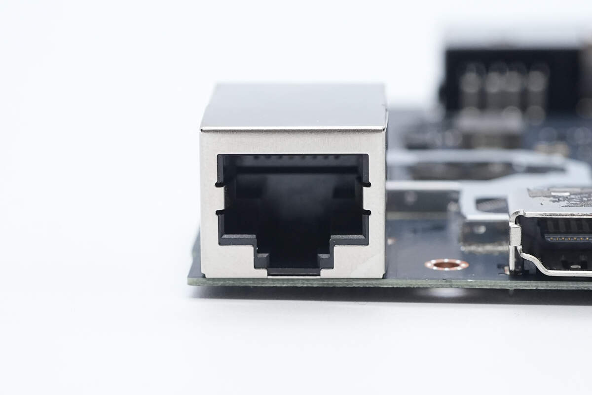
The RJ45 Ethernet port is encased in a metal shield for protection.
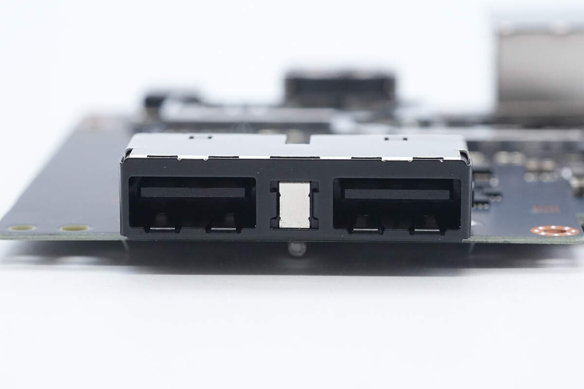
The two USB-A sockets feature an integrated design and are reinforced with a metal casing.

The USB-C output socket has springs on both sides.
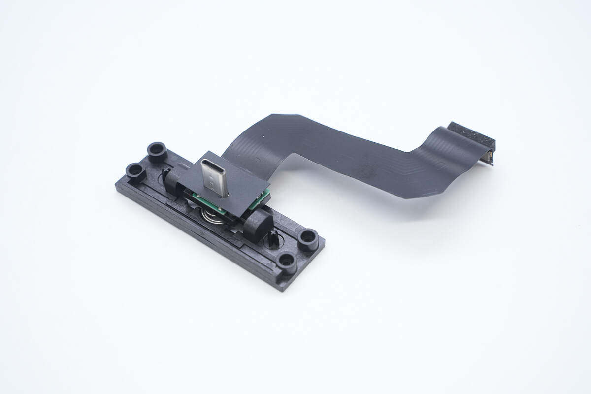
The USB-C male connector is mounted on a separate plastic board.
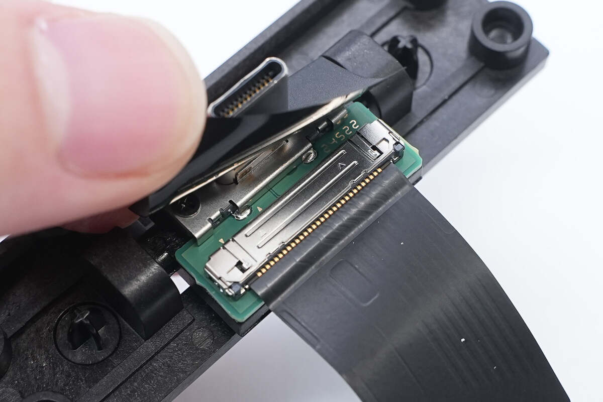
The USB-C male connector is connected to the socket via a ribbon cable.
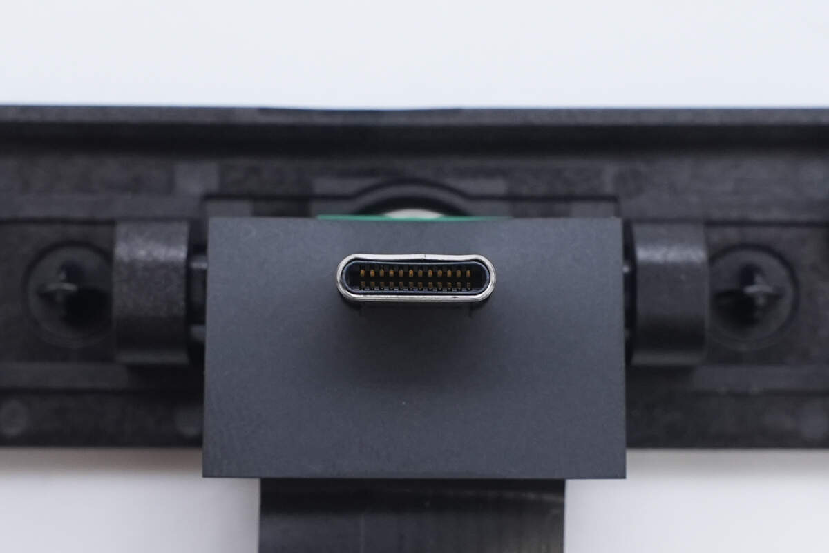
The USB-C male connector features a full-pin design.
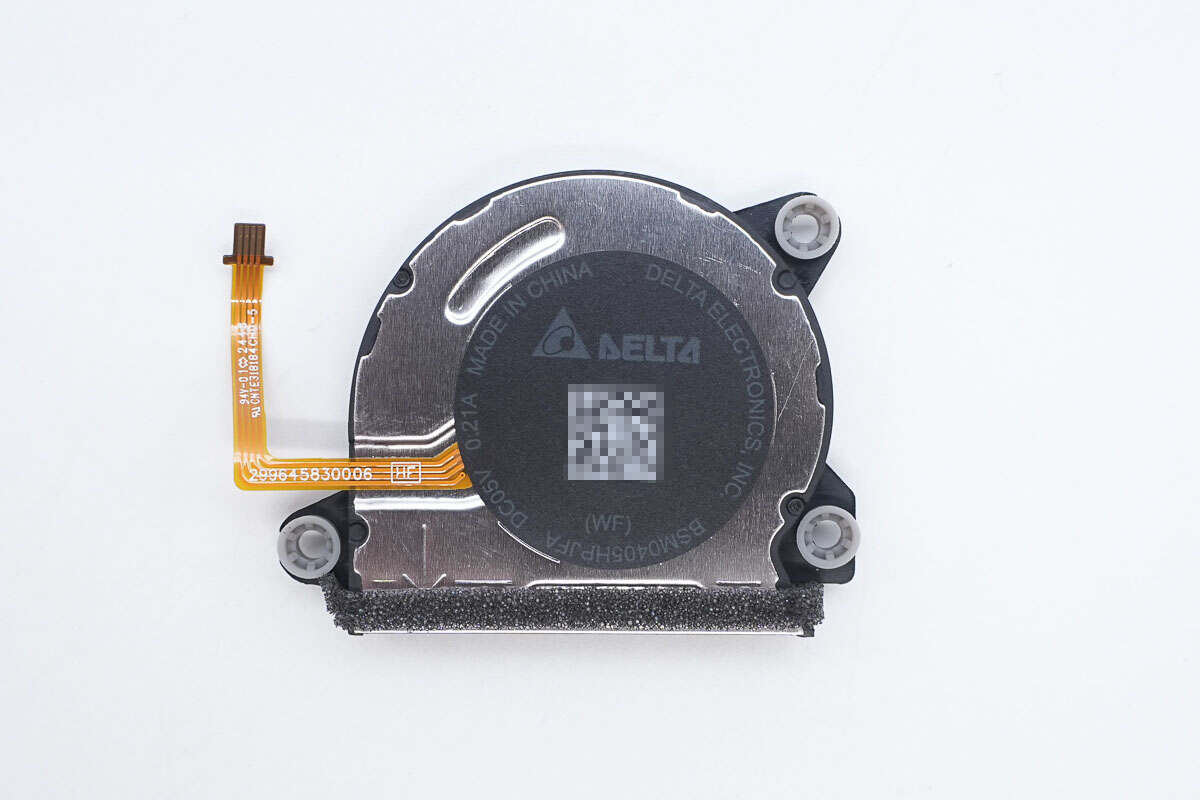
The cooling fan is from Delta, model BSM0405HPJFA, rated at 5V, 0.21A.

Well, those are all components of the Nintendo Switch 2 Official Charging Dock.
Summary of ChargerLAB

Here is the component list of the Nintendo Switch 2 Official Charging Dock for your convenience.
The charging dock retains the classic design, but with more rounded corners. Compared to the previous version, it still features the two key ports: HDMI and gigabit Ethernet. Thanks to the improved performance of the Switch 2, the gaming experience in TV mode is significantly enhanced with higher image quality.
After taking it apart, we found that it uses noticeably upgraded components and, for the first time, includes an active cooling fan to ensure stable long-term operation. The PCB is covered with shielding and heat dissipation metal plates, and the hub circuitry is enclosed under the dedicated shielding cover. Multiple buck circuits are also included in the design. Key components are sourced from internationally recognized manufacturers such as STMicro, TI, Infineon, and REALTEK — all known for their high-performance, reliable chips — ensuring the overall build quality of the dock meets a high standard.
Related Articles:
1. Teardown of SHARGE Pixel 140 GaN Charger (S2)
2. Teardown of MEGMEET MR750‑20V 15 kW DC Charging Module
3. Teardown of Belkin 240W Dual USB-C Braided Cable