Introduction
This teardown features the Moore Threads MTT S70 graphics card. The card utilizes Moore Threads' MUSA unified system architecture, housing 3584 MUSA cores with a core clock speed of 1.6 GHz. It comes equipped with 7GB of GDDR6 memory and delivers a peak single-precision floating-point performance of up to 11.2 TFLOPS, ensuring a smooth user experience.
The MTT S70 features a PCIe 4.0 interface and a triple-fan cooling design, along with the orange ambient lighting. The card is housed in a full-metal chassis and includes three DisplayPort and one HDMI video output connectors. Power is supplied through a PCIe 8-pin power input. Now, let's dive into the teardown of this graphics card and explore its internal structure and design.
Product Appearance

The front of the packaging features the logo, the MTT S70 model name, and an image of the graphics card.
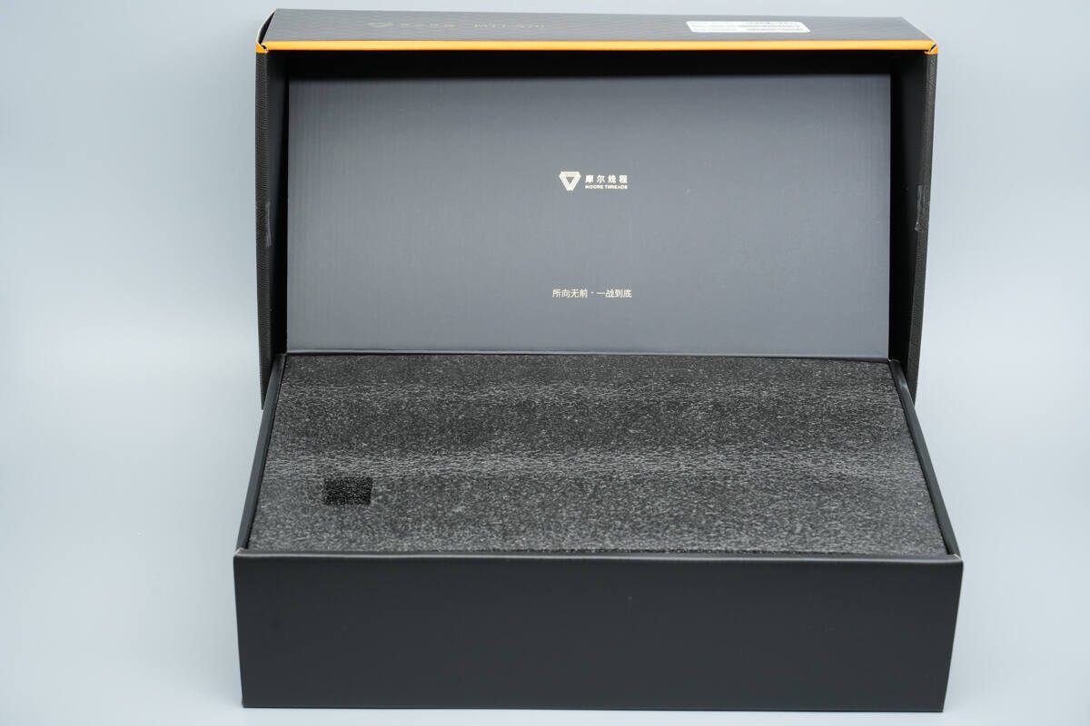
The interior of the packaging is lined with protective foam padding.

The graphics card is wrapped in protective foam.
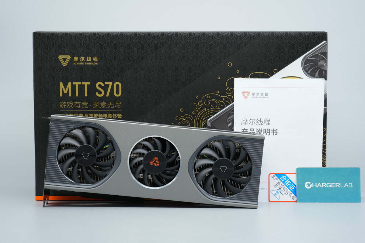
The package includes the MTT S70 graphics card, a product manual, and a quality inspection certificate.
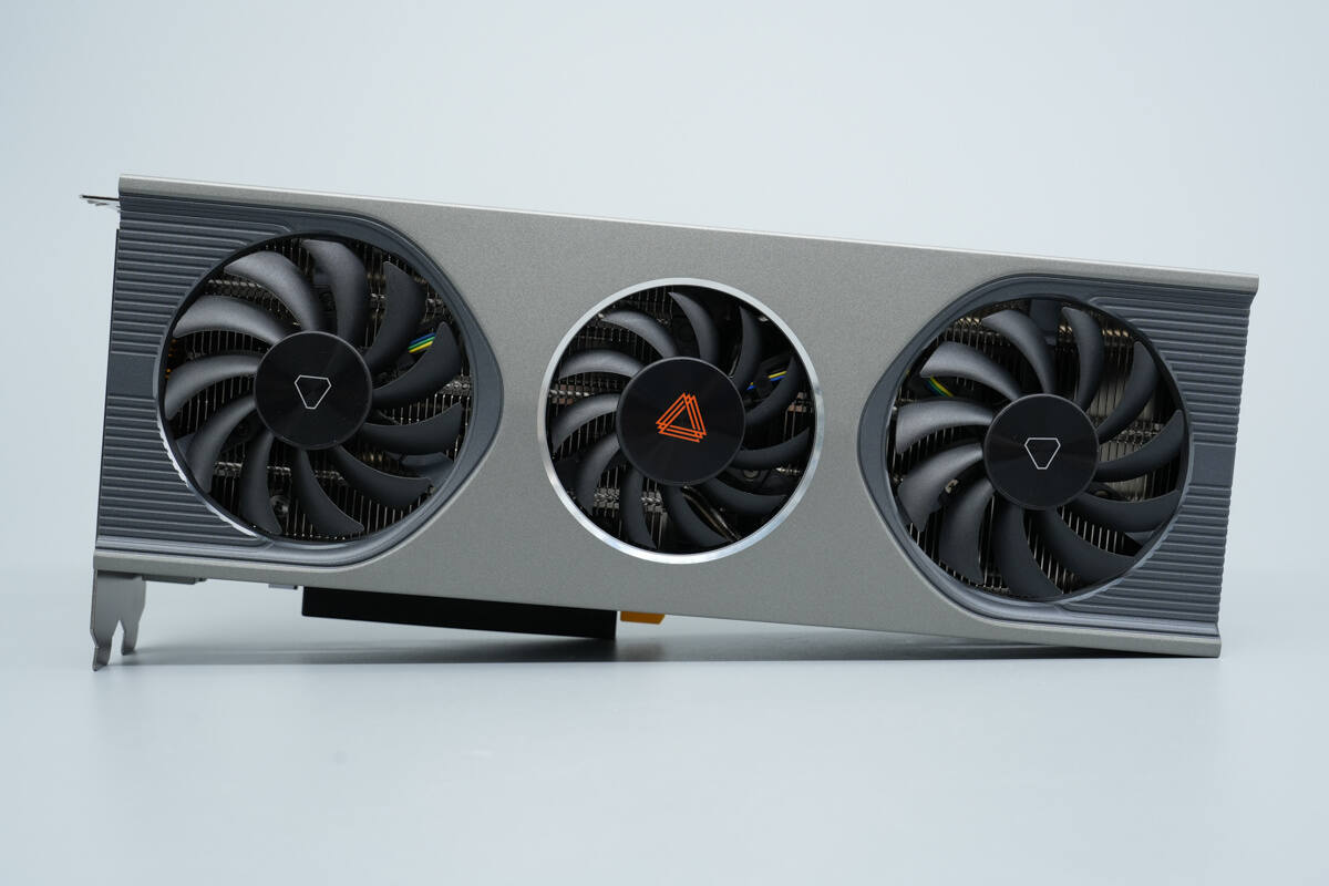
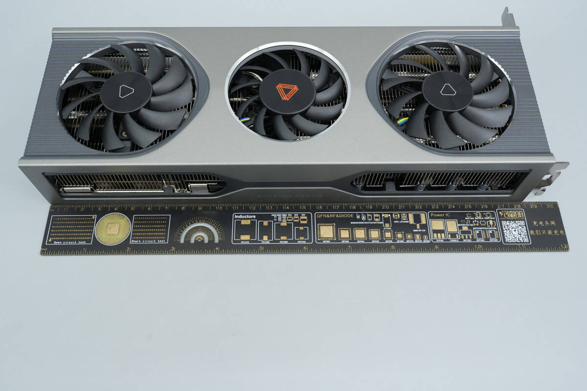
The graphics card features a metal shroud and a triple-fan cooling design.

The backplate is designed with pass-through ventilation openings.

The fans at both ends are large-diameter fans.

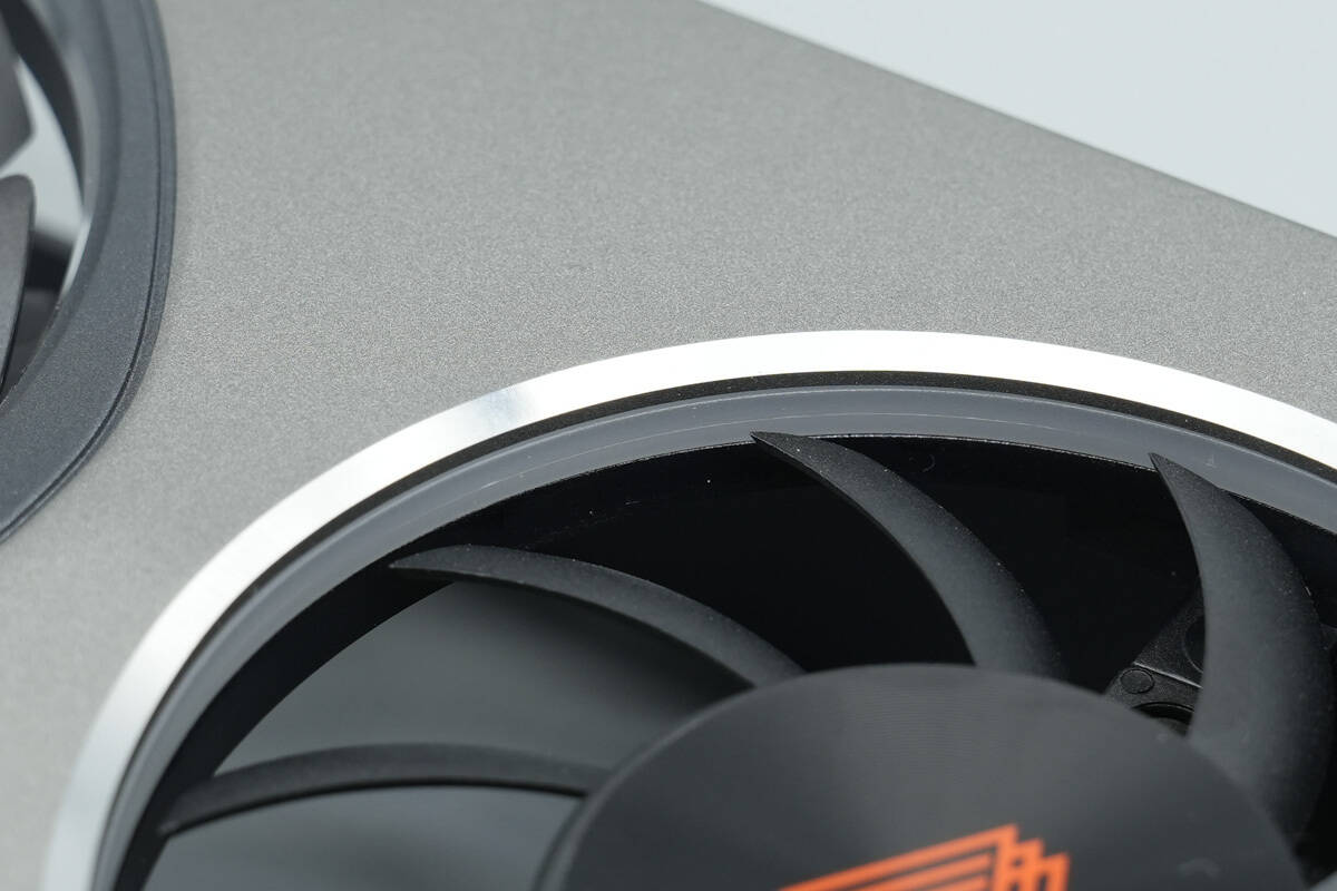
Close-up of the large-diameter fan at the rear.

Close-up of the smaller-diameter fan in the center.
Ambient lighting is installed between the fans and the shroud.
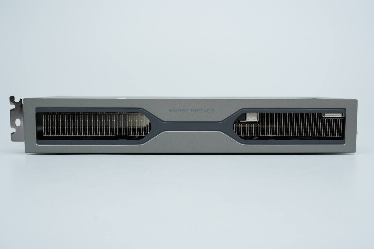
The side features an open design to facilitate hot air exhaust.
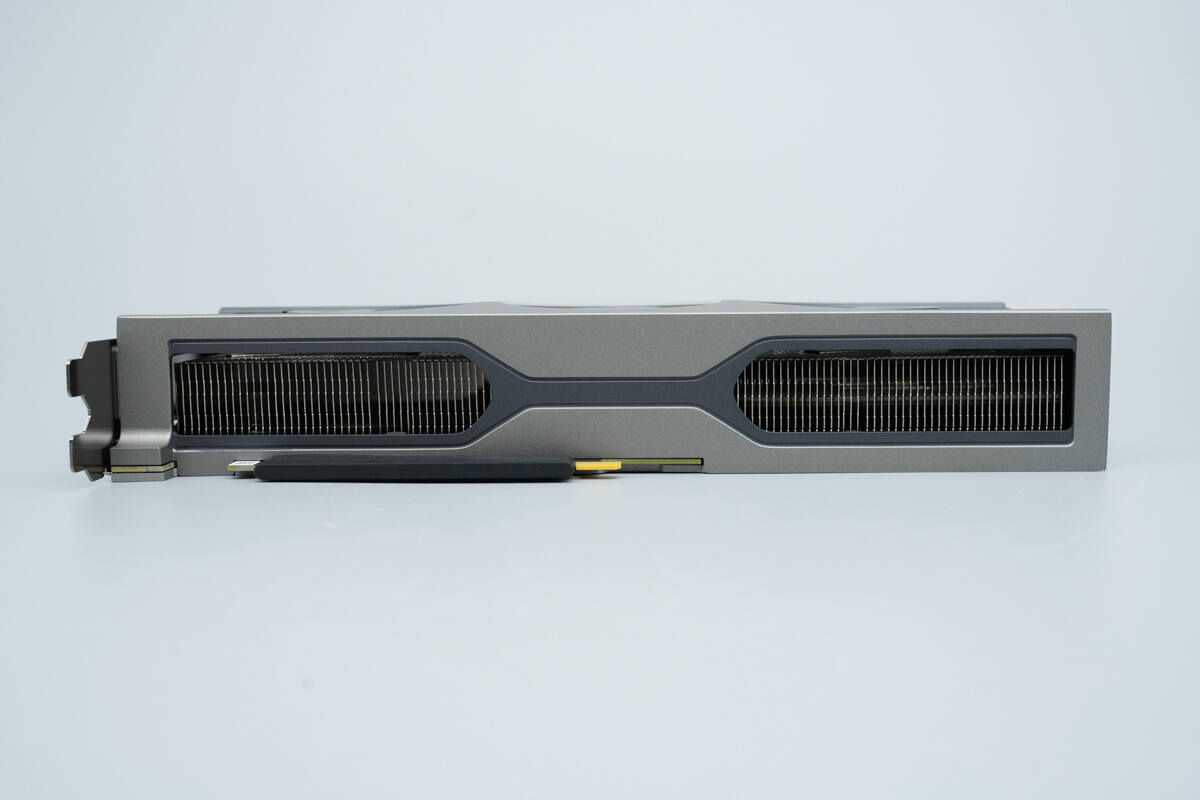
The opposite side also features an open design.
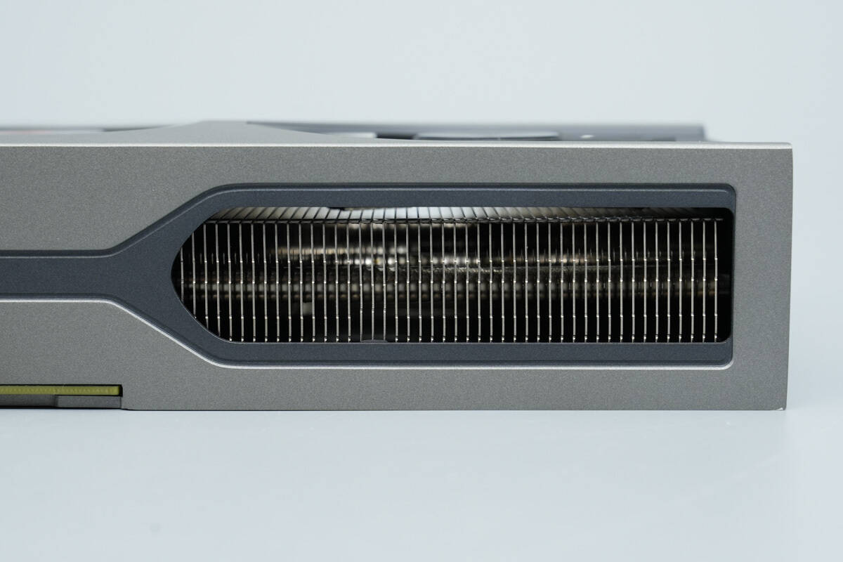
Close-up of the cooling grille.
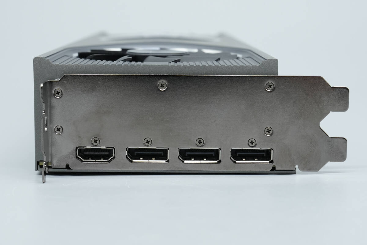
The graphics card has a dual-slot design, with a closed bracket secured to the shroud and ports using screws.

Close-up of the HDMI and DisplayPort connectors.

The rear of the card features a serial number sticker and warning labels, indicating the PCIe 8-pin power connector.
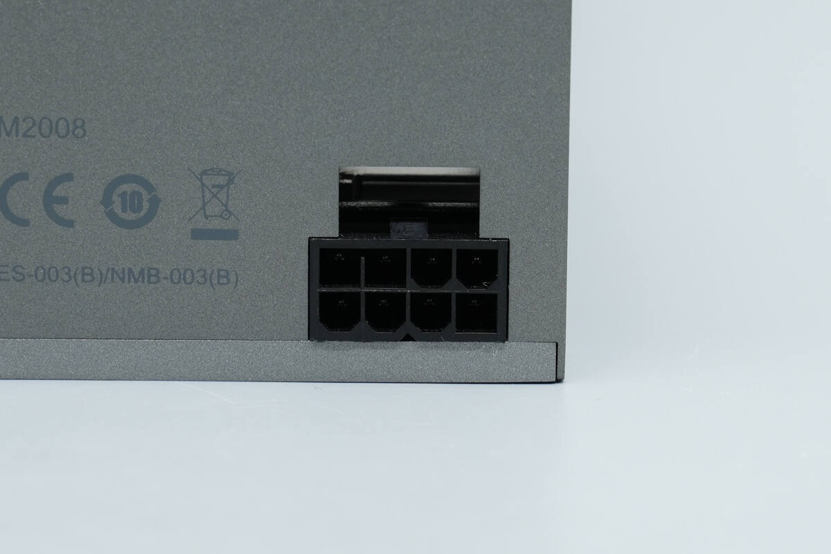
After removing the warning label sticker, the PCIe 8-pin power connector is exposed.

The gold finger connector is marked with the Moore Threads logo.
The length of the graphics card is about 285 mm (11.22 inches).
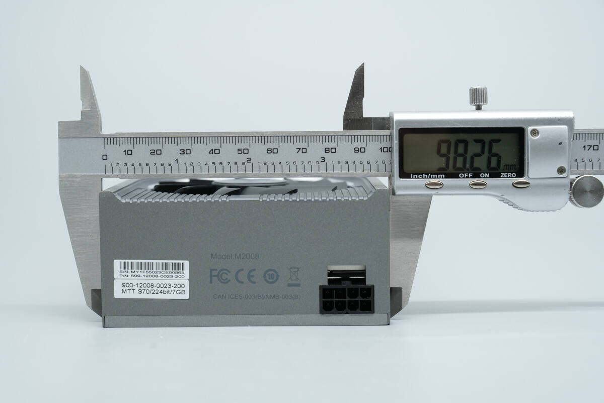
The width is about 98.3 mm (3.87 inches).
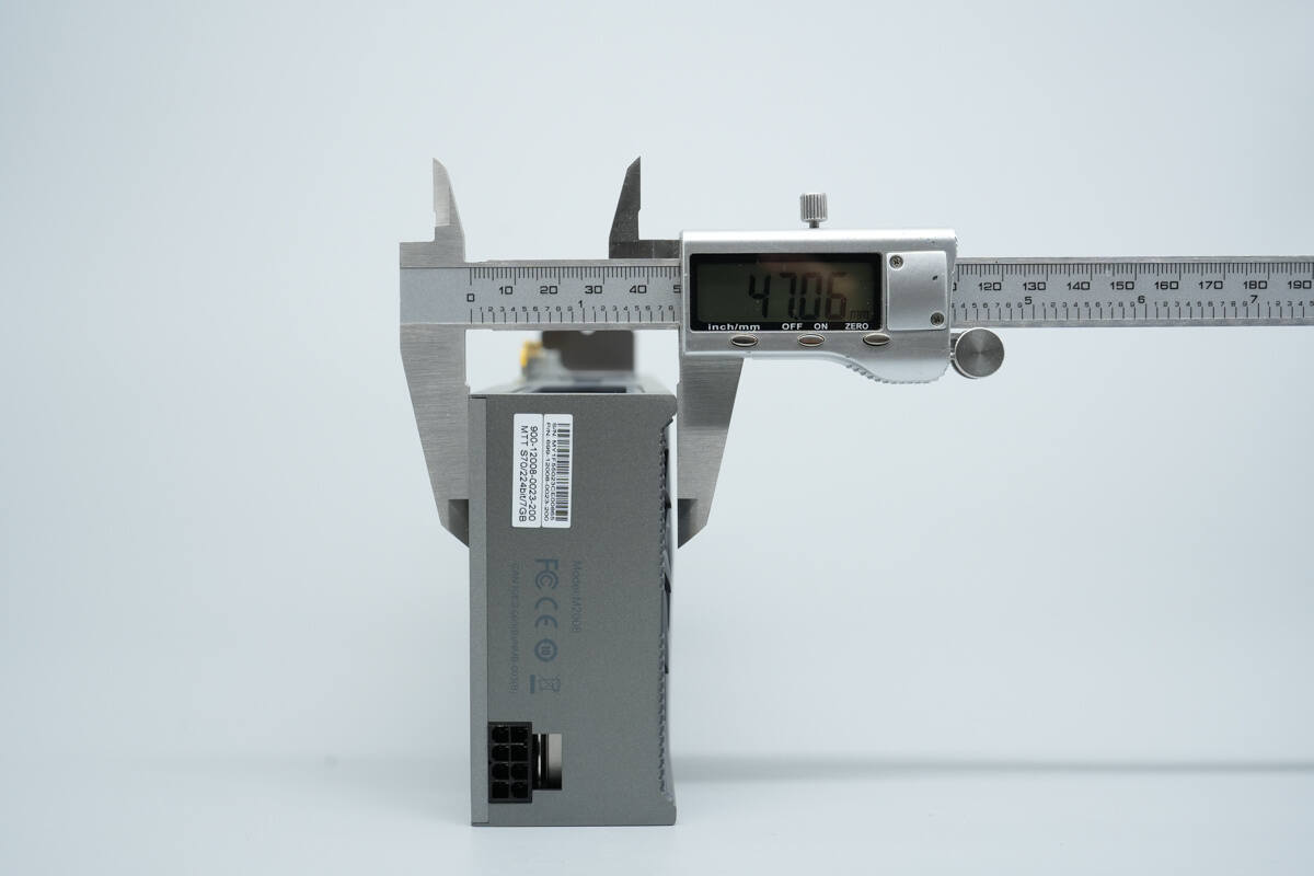
The thickness is about 47.1 mm (1.85 inches).
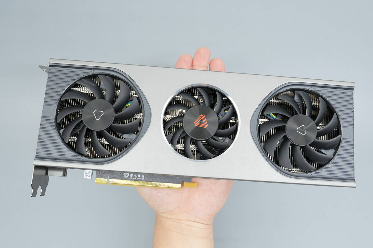
That's how big it is on the hand.
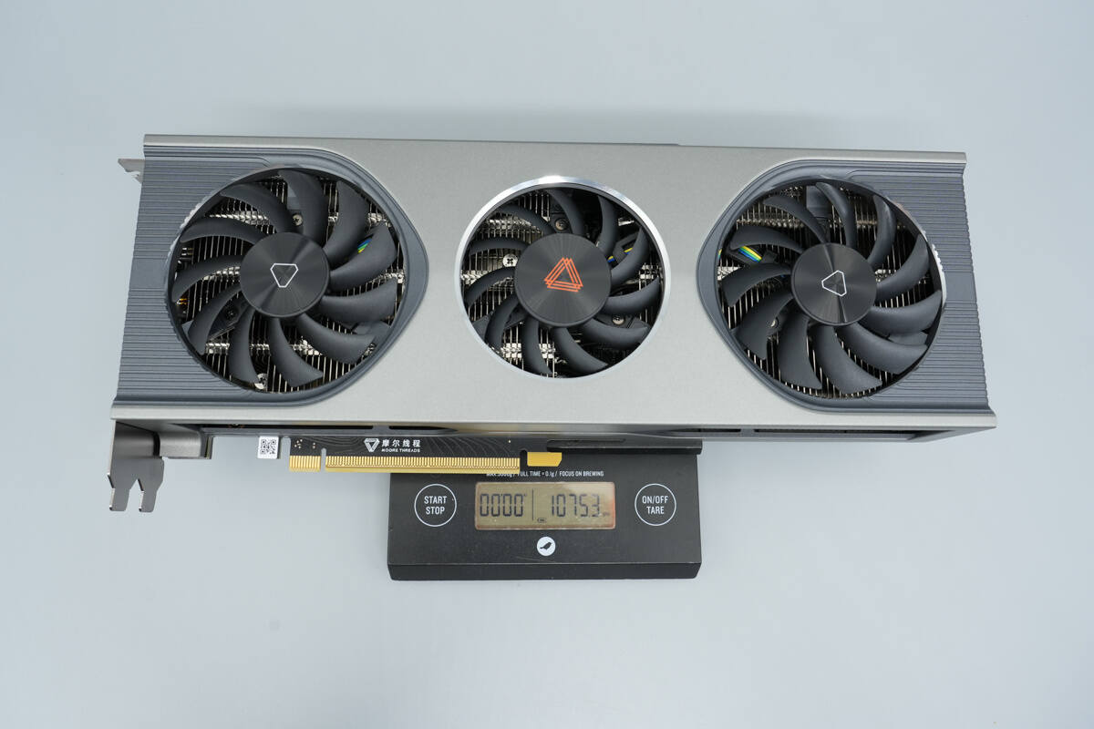
The weight is about 1075.3 g (37.93 oz).
Teardown
Next, let's take it apart to see its internal components and structure.

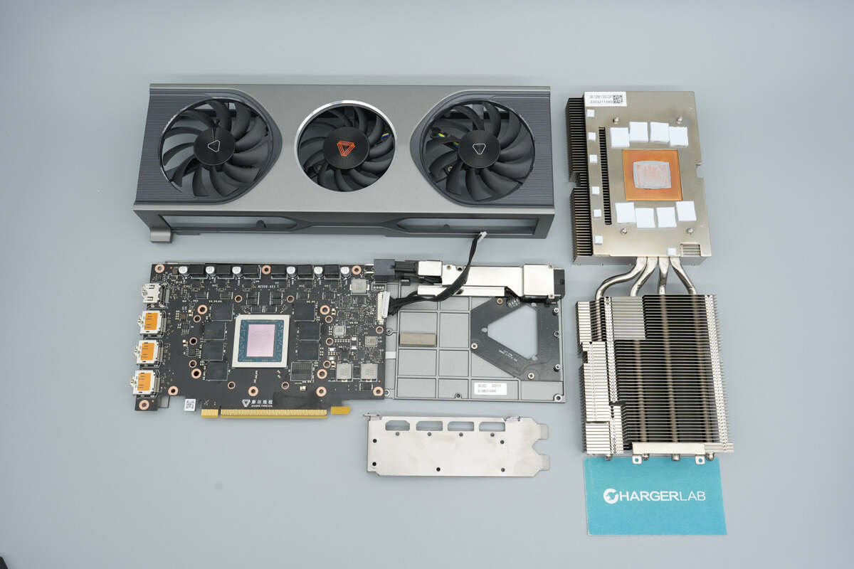
Remove the screws and remove the shroud and side brackets.

The fans and ambient lighting are connected to the graphics card PCB via wires.
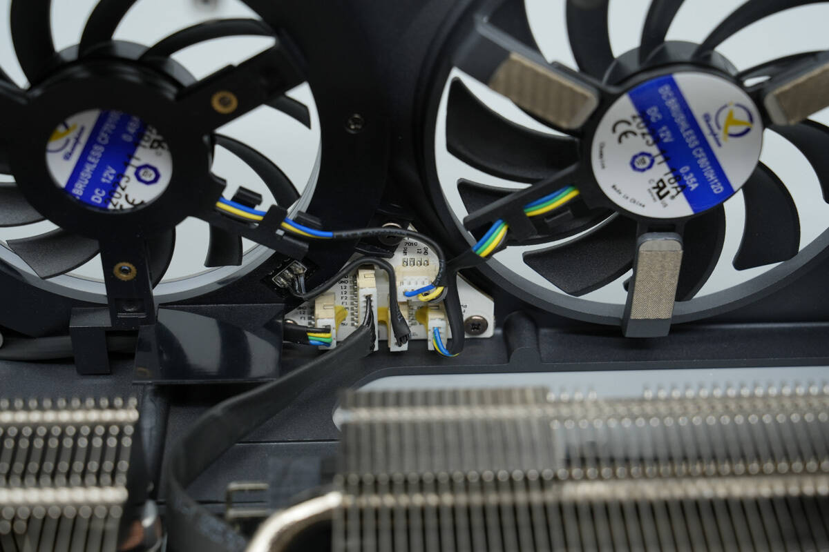
The fans and ambient lighting are connected to a small PCB via connectors.

The cooling fans are from Dongguan Champion Electronic Technology Co., Ltd., model CF8010H12D, rated at 12V 0.35A.
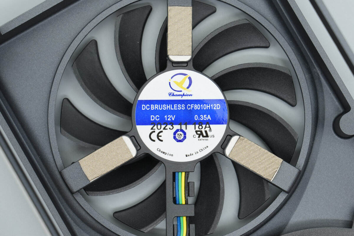
The other cooling fan has the same model.
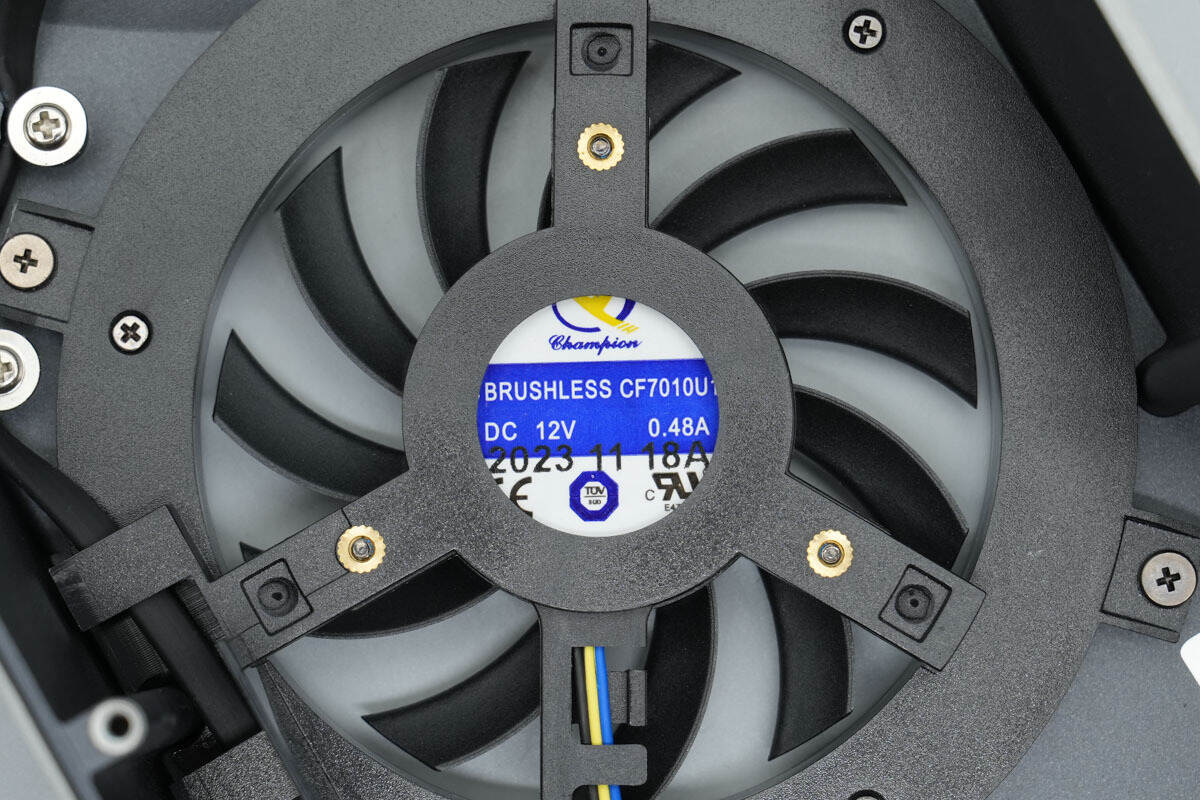
The smaller-diameter fan in the center is model CF7010U1, rated at 12V 0.48A.
The cooling assembly is secured to the aluminum alloy backplate with screws.

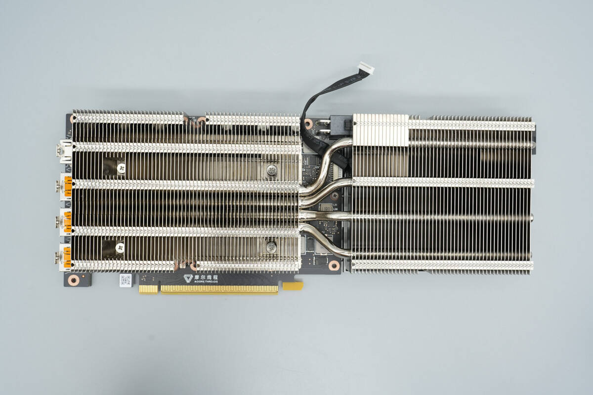
The cooling assembly features a four-heat-pipe design.

Remove the screws and remove the bracket and cooling assembly to continue the teardown.
Overview of the back of the cooling assembly, with heat pipes connecting to the right-side fins for heat dissipation.

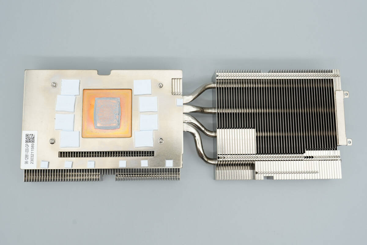
The heatsink has a copper base aligned with the GPU core, and thermal pads are placed over the memory chips and DrMOS components.

The PCB module is secured to the backplate with screws.
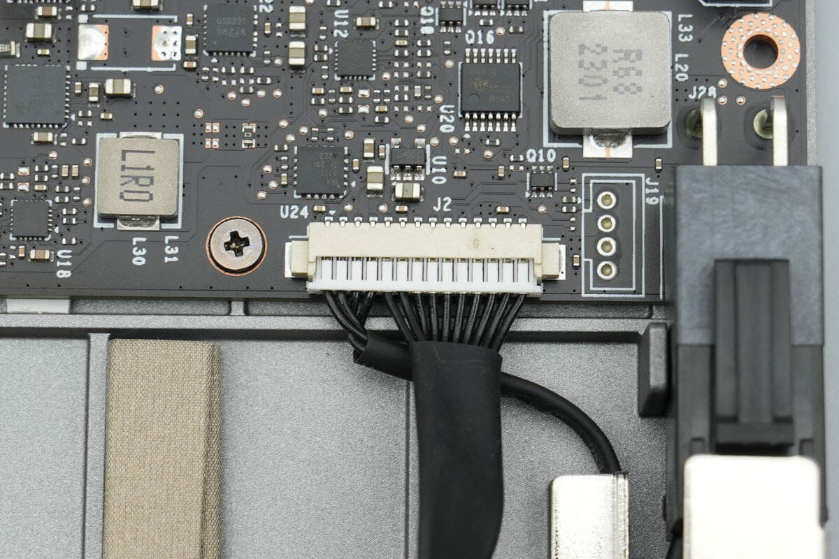
Close-up of the connector for the cooling fans and ambient lighting.
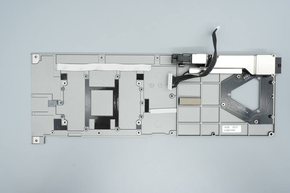
Remove the PCB module. An insulating sheet is attached to the backplate where the PCB module was mounted, thermal pads are placed over the DrMOS components, and a power adapter cable is located at the upper-right corner.

Close-up of the ambient lighting at the rear.

Front view of the PCB module: the GPU core is located in the center, with four memory chips on the left and three memory chips on the right. Above the GPU are filter capacitors, buck inductors, and DrMOS components. On the left side are the HDMI and DisplayPort connectors. The lower-right corner houses additional buck inductors, DrMOS components, and filter capacitors.
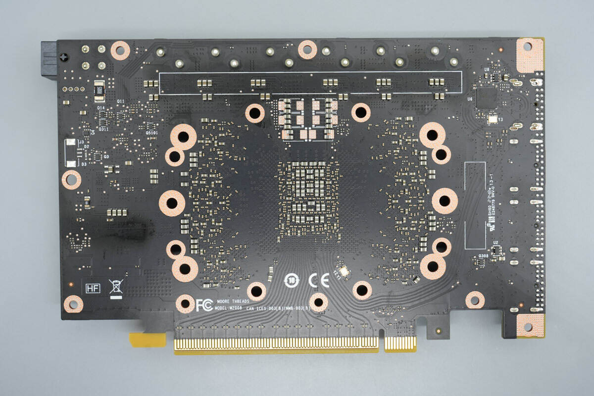
On the back side, there is a current-sensing resistor, a filter MLCC capacitor, and a video conversion chip.

The MTT S70 GPU is marked with SD102AA-400 BCDAE.001 05ODA6 A1AA. It features 3,584 MUSA cores with a clock speed of 1.6 GHz and delivers a peak single-precision floating-point performance of 11.2 TFLOPS. The GPU is paired with 7 GB of GDDR6 high-speed memory, featuring a 224-bit memory bus and a bandwidth of 392 GB/s.
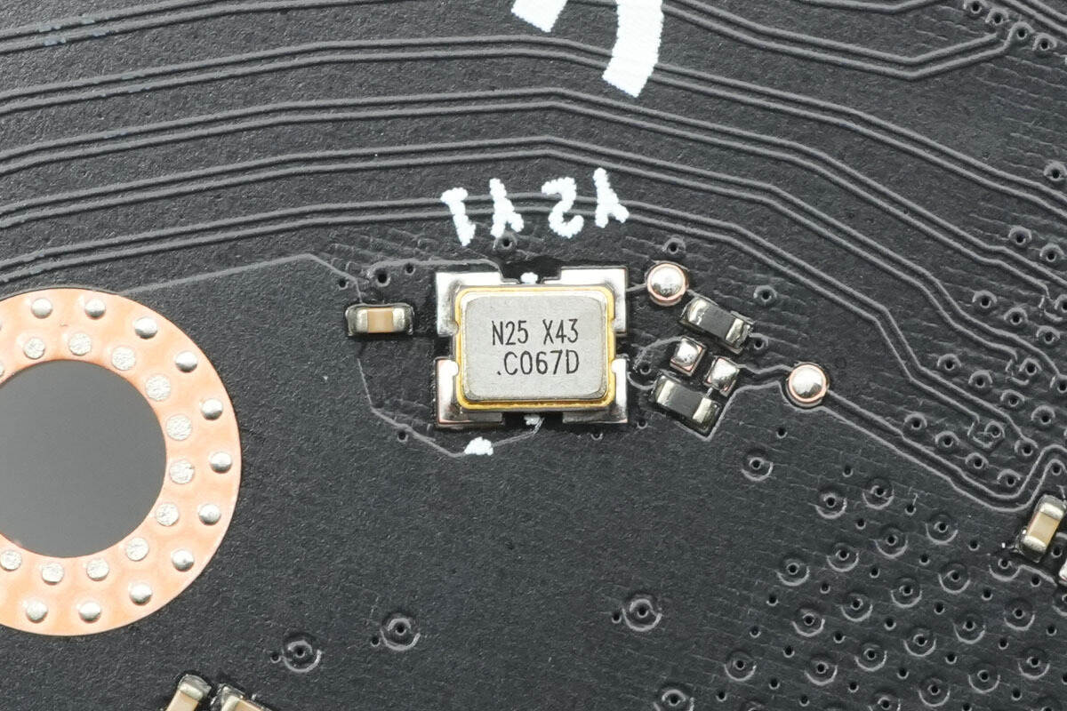
Close-up of the external clock crystal.
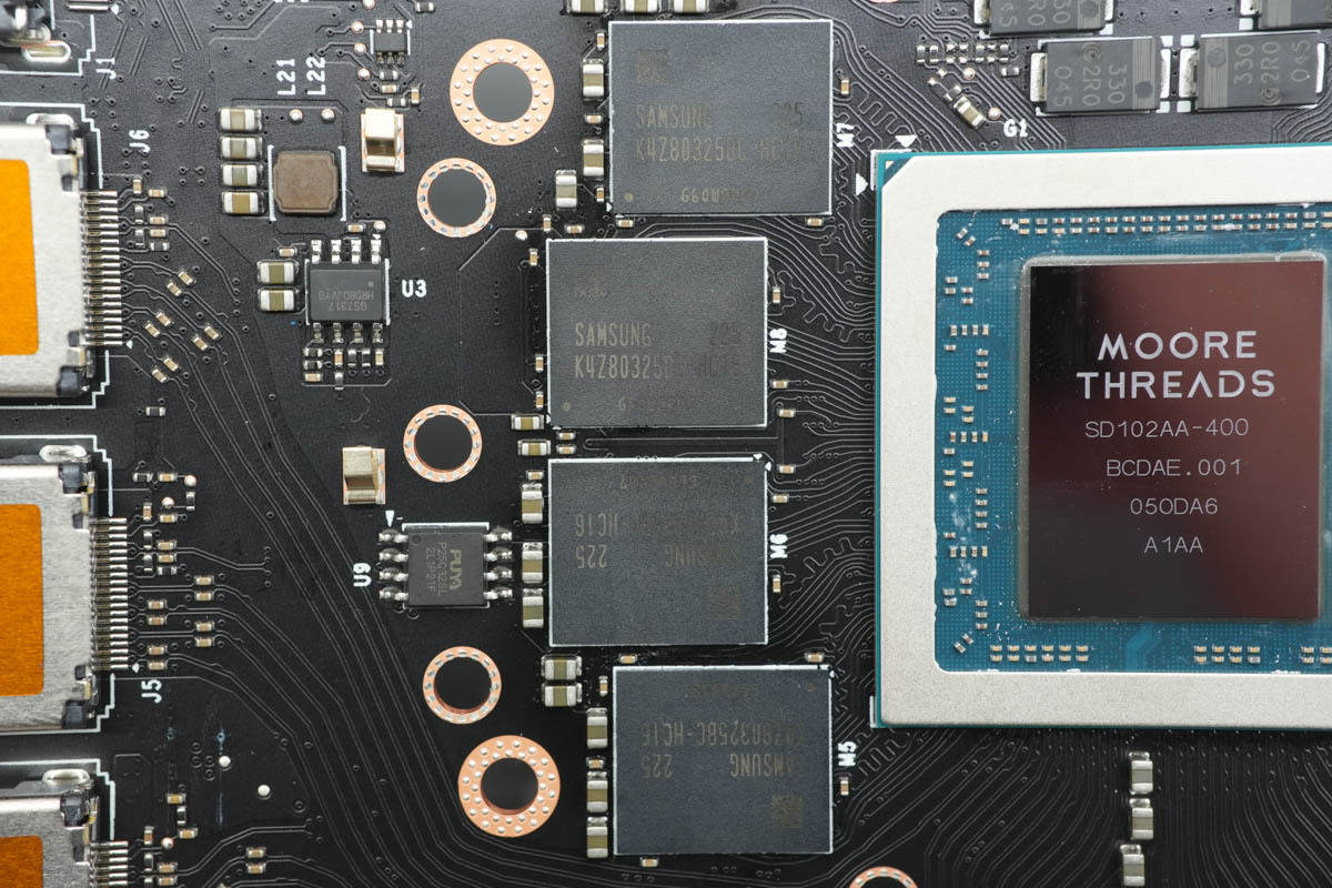
Close-up of the four memory chips on the left side of the GPU.

Close-up of the three memory chips on the right side of the GPU.

The memory chips are from Samsung, model K4Z80325BC-HC16, each with a capacity of 1 GB, a speed of 16 Gbps, and packaged in 180 FBGA.

The memory is from Puya, model P25Q32SL, with a capacity of 32 Mb, supporting a 1.65–2 V operating voltage, and comes in an SOP8 package.
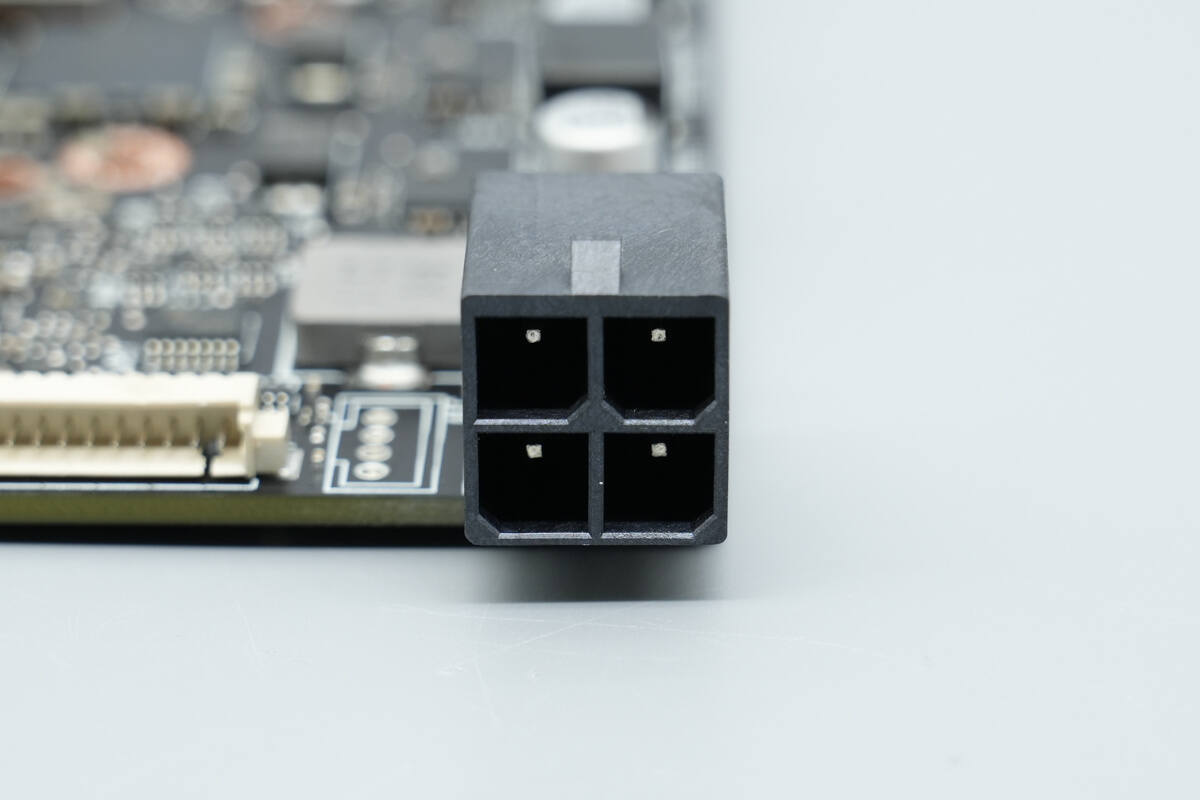
The power connector is a 4-pin design.
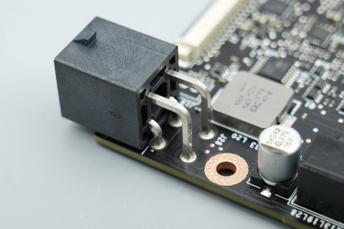
The connector is soldered to the PCB module.

A 0.68 μH SMD inductor is used for power filtering.

A 5 mΩ shunt resistor is used to monitor the input current.

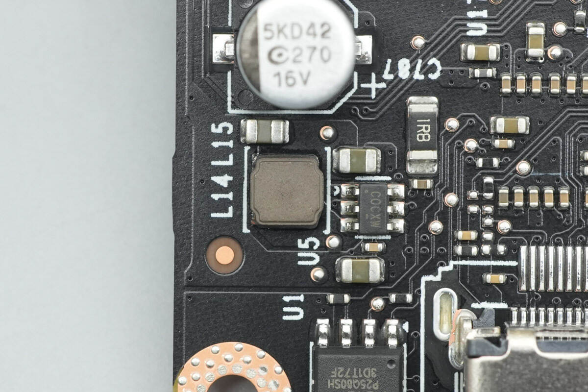
The input filter capacitor is from APAQ, AV5K series, with a lifespan of 5000 hours, an operating temperature range of -55 to 105 °C, and a rating of 270 μF 16 V.

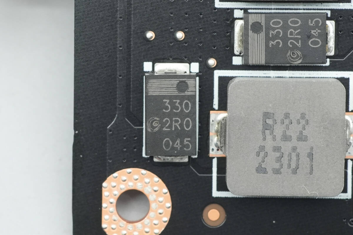
The inductors are through-hole mounted and marked with LR22.

The output filter capacitors are from APAQ, surface-mount conductive polymer solid capacitors, rated at 330 μF 2 V.

Close-up of the two 0.22 μH buck inductors in the lower-right corner.
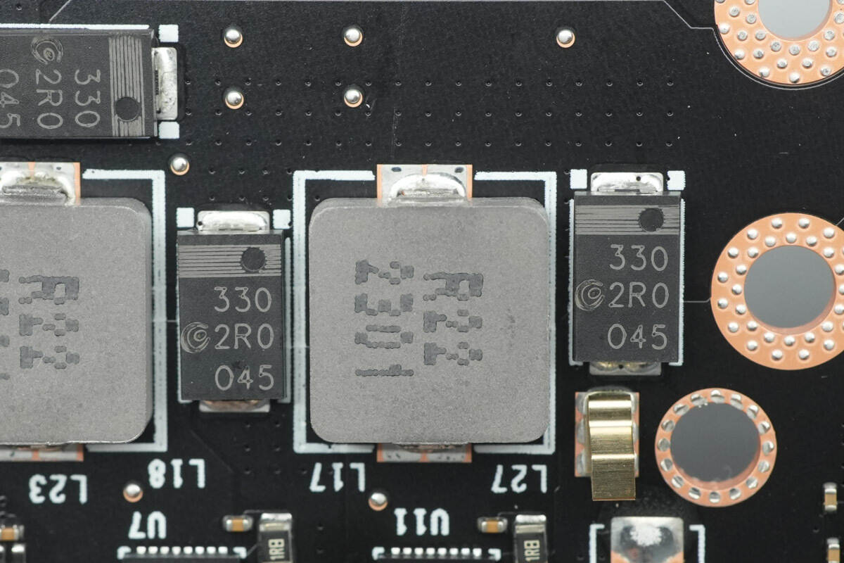
The filter capacitors are rated at 330 μF 2 V.
The other filter capacitor has the same rating.
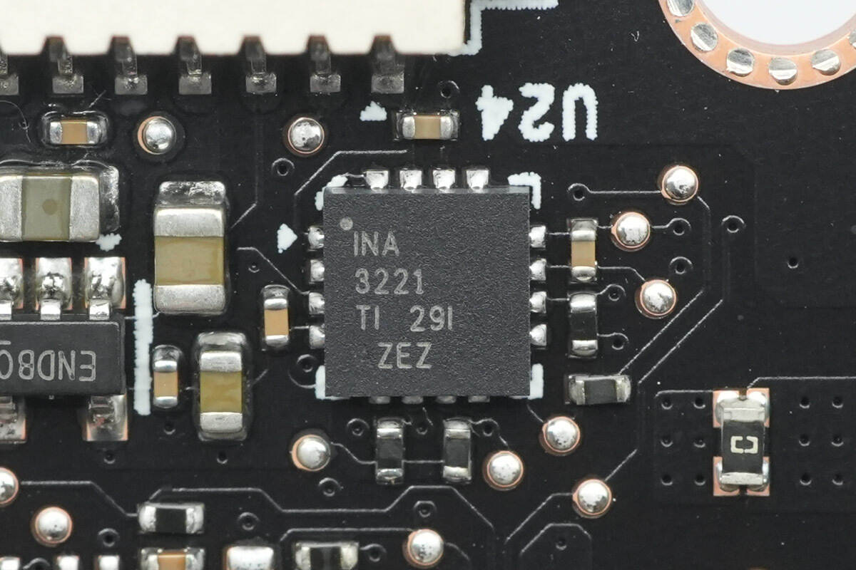
The power monitoring chip is from Texas Instruments, model INA3221. It is a three-channel voltage and current monitor supporting I²C and SMBus interfaces, capable of measuring up to 26 V. It has two current channels, a built-in 13-bit ADC, supports an operating voltage range of 2.7–5.5 V, features programmable alert and warning outputs, and comes in a VQFN16 package.
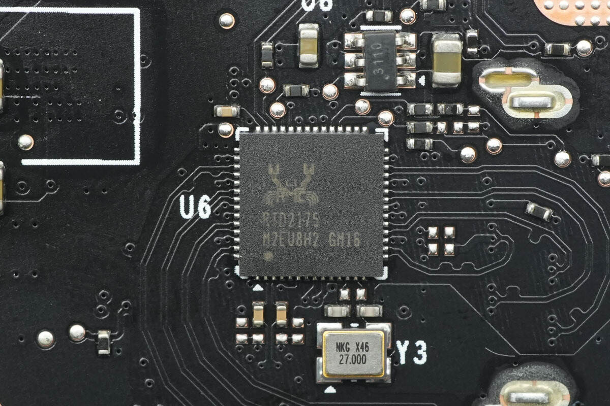
The video conversion chip is from Realtek, model RTD2175, used for converting DisplayPort to HDMI output, and comes in a QFN56 package.

Close-up of the 27.000 MHz clock crystal.

The memory is from Puya, model P25Q80SH, with a capacity of 8 Mb, supporting a 2.3–3.6 V operating voltage, and comes in an SOP8 package.
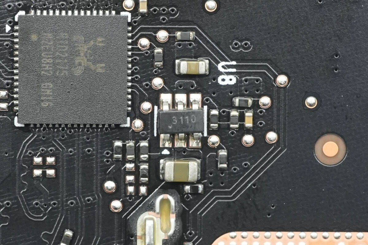
The charge pump is from SGMicro, marked 3110, model SGM3110-5.0. It is a low-power charge-pump boost converter with a 5 V output, supporting a 2.7–5 V input voltage, 100 mA output current, and a switching frequency of 750 kHz. It features short-circuit and over-temperature protection and comes in a SOT-23-6 package.

The load switch is from GStek, marked END, model GS7615. It supports a 2.5–5.5 V input voltage, features an integrated internal MOSFET, and comes in a SOT-23-5 package.

The other load switch has the same model.

A 1 μH inductor is used for power filtering.
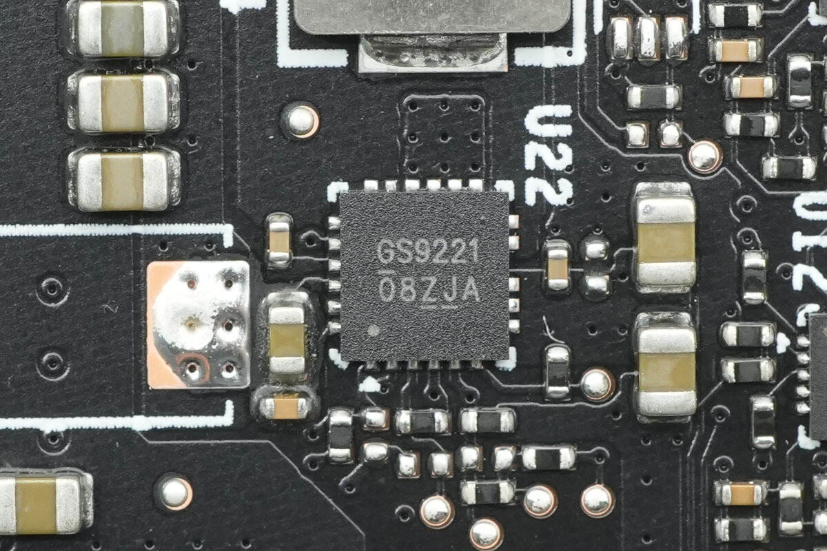
The synchronous buck chip is from GStek, model GS9221. It is a high-performance synchronous buck converter supporting a 2.7–26 V input voltage and 0.6–12 V output voltage, with a 6 A output current. The chip integrates internal MOSFETs, supports a 100–600 kHz switching frequency, and features over/under-voltage protection, over-temperature protection, and over-current protection. It comes in a TQFN23 package.

Close-up of the 1 μH buck inductor used with the chip.
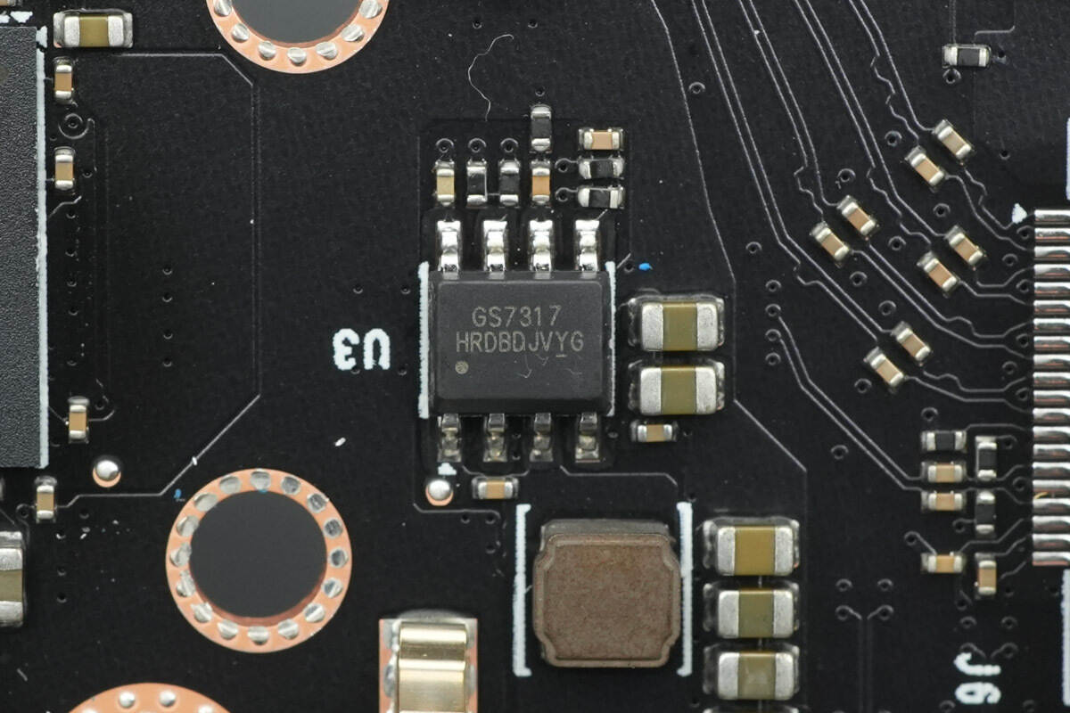
The synchronous buck chip is from GStek, model GS7317. It is a high-performance synchronous buck converter supporting a 4.5–23 V input voltage and 0.8–20 V output voltage, with a 3 A output current. The chip integrates internal MOSFETs, operates at a 340 kHz switching frequency, and features over-current protection, output under-voltage protection, and over-temperature shutdown protection. It comes in a PSOP-8 package.

Close-up of the buck inductor used with the chip.
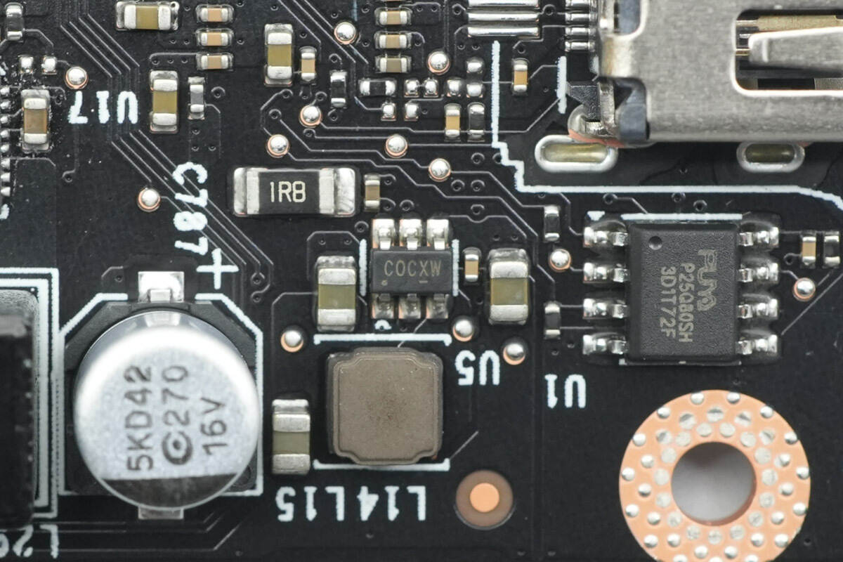
The synchronous buck chip is from GStek, marked COC, model GS7316. It is a high-performance synchronous buck converter supporting a 2.8–5.5 V input voltage and a 3 A output current. The chip integrates internal MOSFETs, operates at a 1 MHz switching frequency, and features built-in short-circuit and over-temperature protection. It comes in a SOT-23-6 package.
Close-up of the buck inductor used with the chip.

The flip-flop is from Texas Instruments, marked HCS72, model SN74HCS72. It is a dual negative-edge-triggered D-type flip-flop with Schmitt-trigger inputs, featuring clear and preset pins, and comes in a TSSOP14 package.
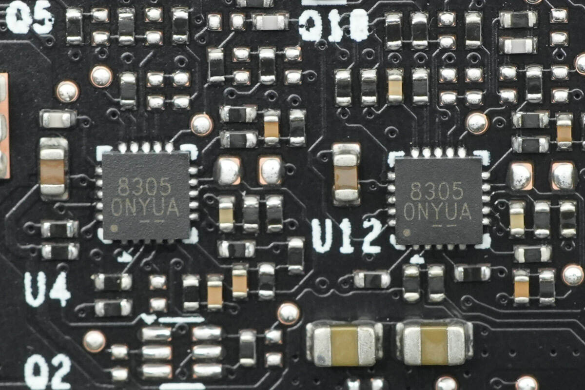
Close-up of the two chips marked 8305.

The other chip is marked the same.
Well, those are all components of the Moore Threads MTT S70 Graphics Card.
Summary of ChargerLAB
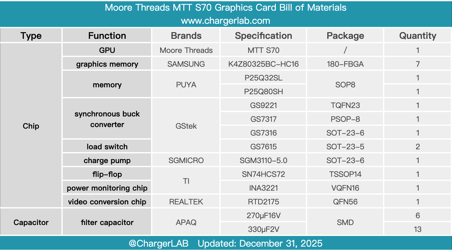
Here is the component list of the Moore Threads MTT S70 Graphics Card for your convenience.
It features an aluminum alloy shroud, three cooling fans, and includes three DisplayPort and one HDMI connectors. It utilizes a PCIe 8-pin power connector, features 7 GB of GDDR6 memory, and achieves a peak single-precision floating-point performance of 11.2 TFLOPS.
After taking it apart, we found that it uses an aluminum alloy backplate with thermal pads on the back of the DrMOS components. It features the MTT S70 GPU, paired with seven Samsung K4Z80325BC-HC16 memory chips, with thermal pads on the front of the memory making contact with the cooling assembly.
The power input uses APAQ solid-state capacitors, while the buck output uses APAQ capacitors. The cooling assembly features a four-heat-pipe design, with a copper base directly over the GPU to enhance heat transfer. Combined with the open-side design, it promotes airflow and provides efficient cooling.
Related Articles:
1. Teardown of Pisen 160W 4-USB-C GaN Charger (TP-C81)
2. Teardown of Highsay C1 Pro 140W Ultra Charger
3. Teardown of Belkin BoostCharge Pro 140W Braided USB-C to Dual USB-C Cable (CAC004)