Introduction
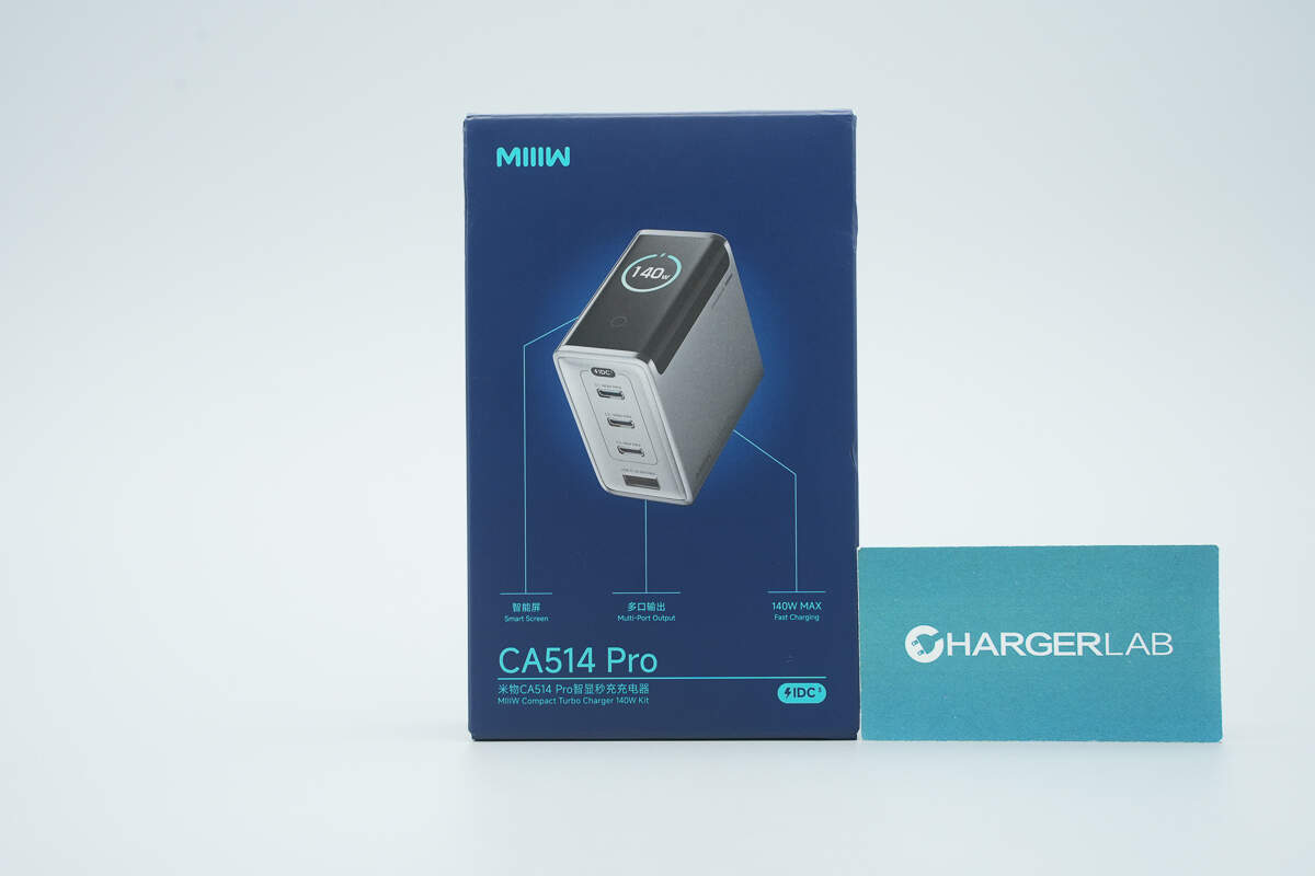
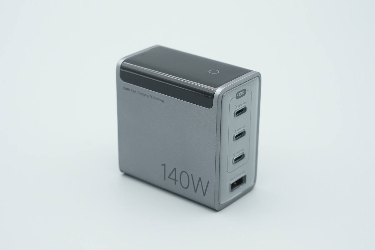
MIIIW has released a 140W GaN Charger. It features three USB-C and one USB-A. It supports both 140W PD 3.1 fast charging and Xiaomi’s 120W Surge fast-charge protocol. The charger is equipped with a borderless TFT display capable of showing detailed information such as per-port output power, total power, temperature, and other real-time metrics. Next, let’s take a closer look at its internal components and design.
Product Appearance
The front of the packaging box displays the MIIIW branding, the product image, key selling points, and the product name.

The back of the packaging features product usage scenarios along with specifications.

The package includes the charger, a data cable, the user manual, and related documentation.
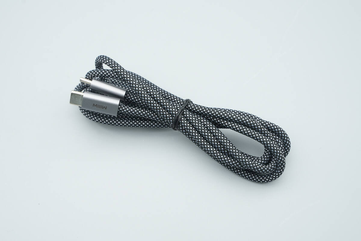
The included cable is a braided design and supports up to a 6A current.
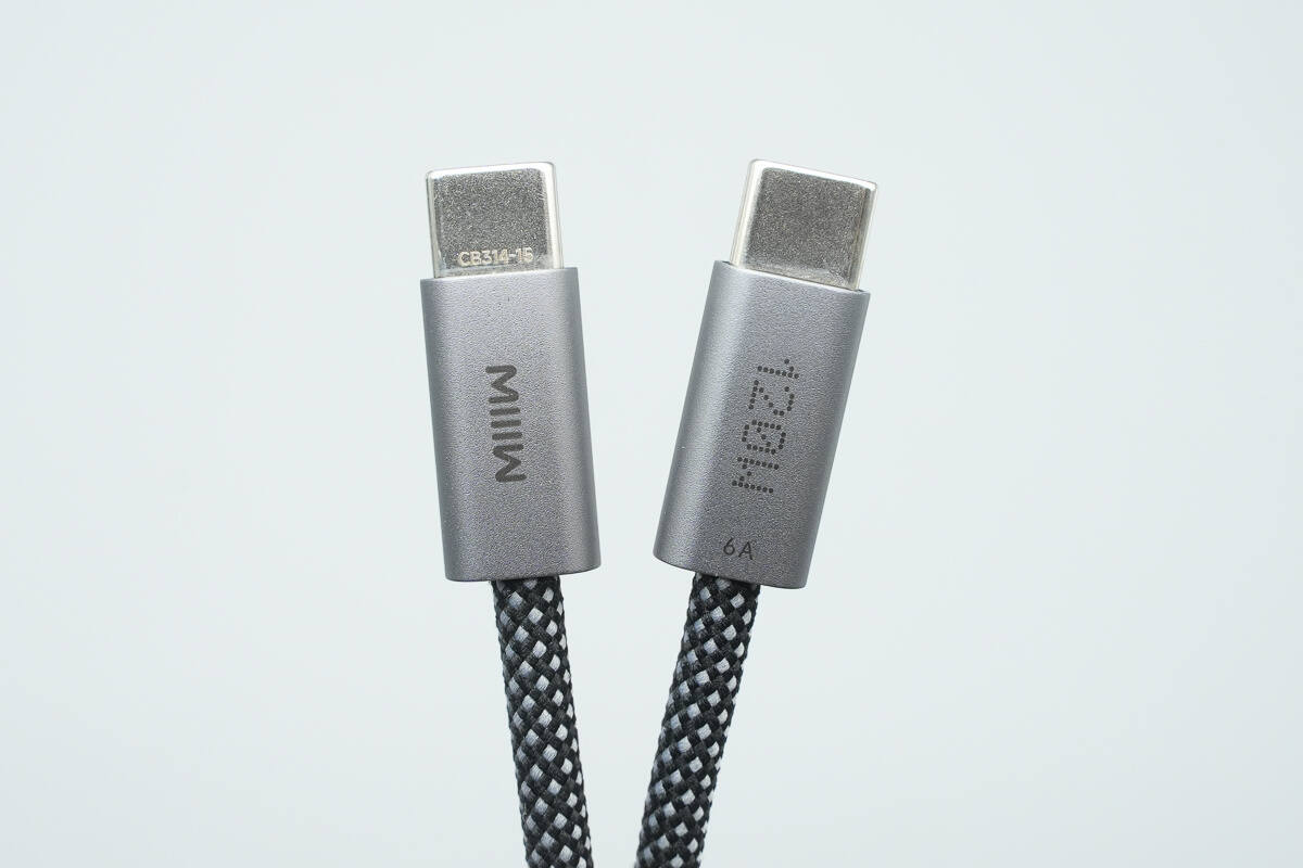
The connectors are labeled with the MIIIW logo along with the markings 120W and 6A.
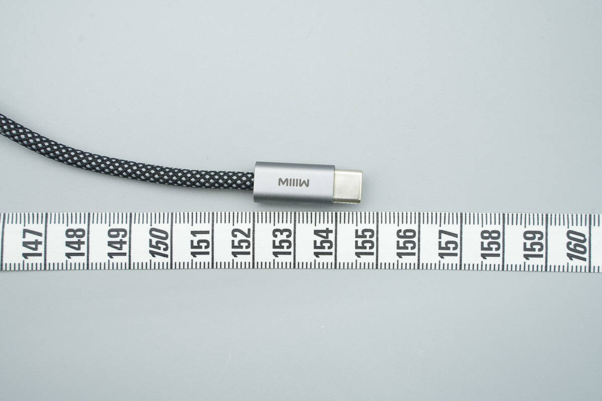
The length of the cable is about 154.5 cm (60.83 inches).
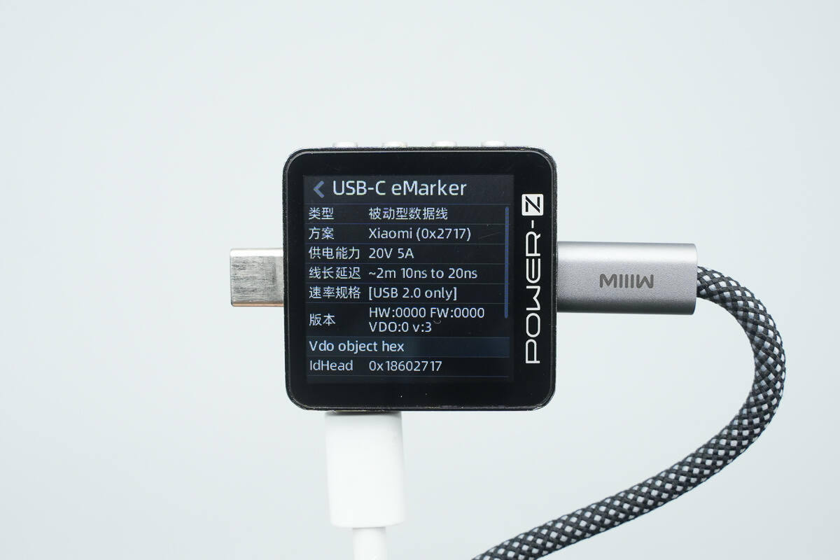
ChargerLAB POWER-Z KM003C shows it has an E-Marker chip. Its power transmission capability is 20V5A, while its data transfer capability is USB 2.0. Therefore, the cable is compatible with 100W PD fast charging and Xiaomi’s 120W Surge fast charging. To achieve 140W PD 3.1 fast charging, a separate cable is required.
The enclosure is made of flame-retardant PC material, with a silver-gray metallic coating applied to the surface.
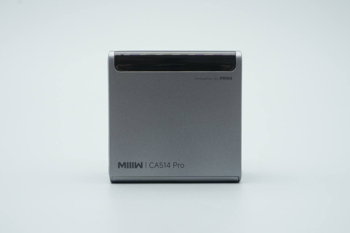
The front side is printed with the MIIIW logo, the model designation CA514 Pro, and the tagline “innovation by MIIIW.”
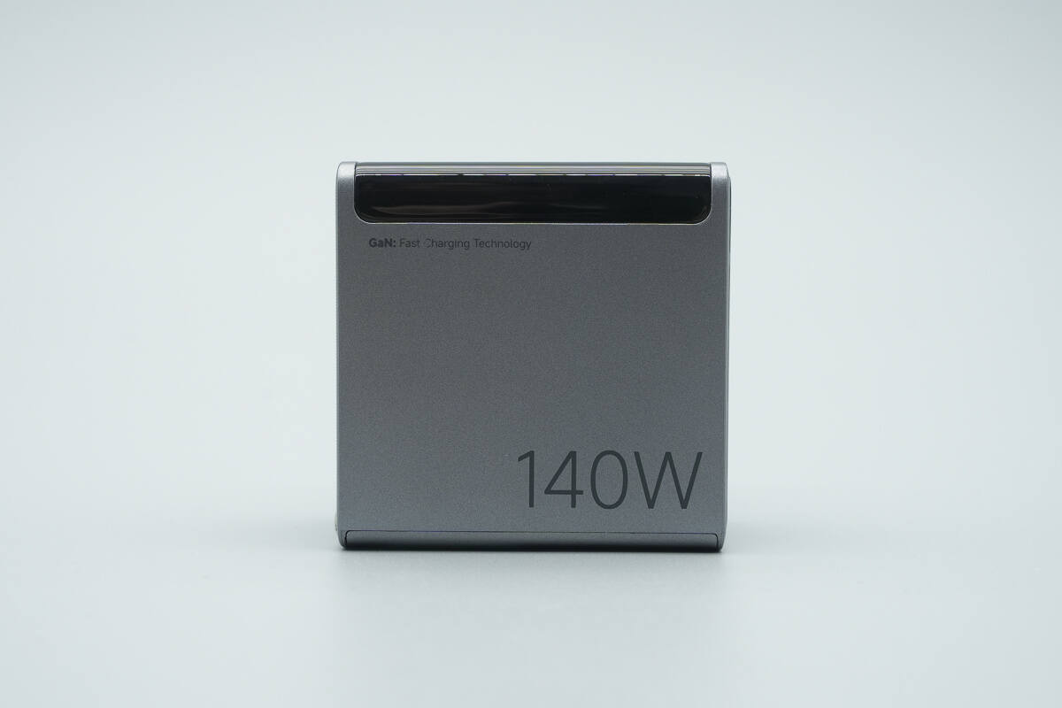
The other side is marked with “140W” and “GaN: Fast Charging Technology.”
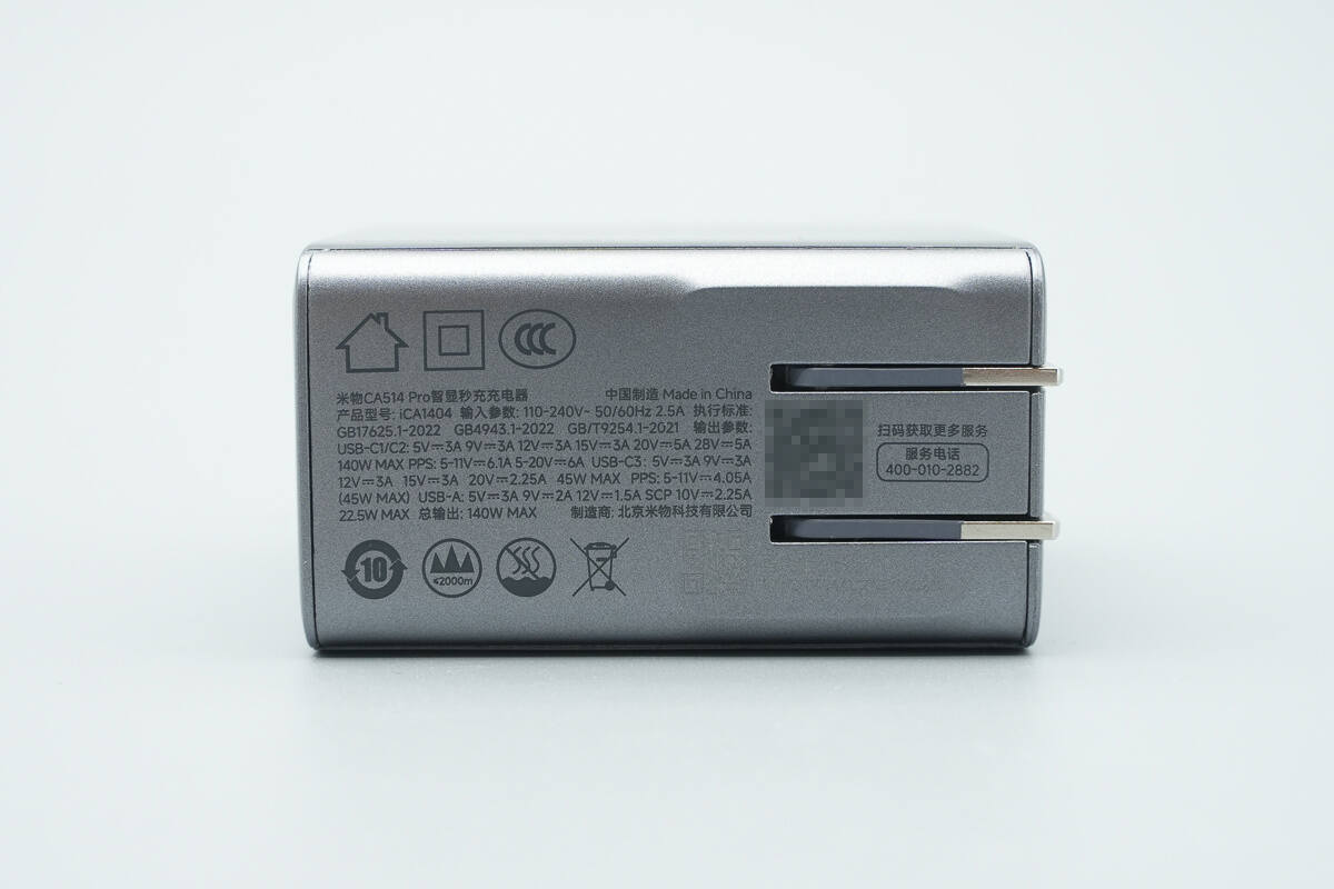
The bottom of the charger displays the product specifications.
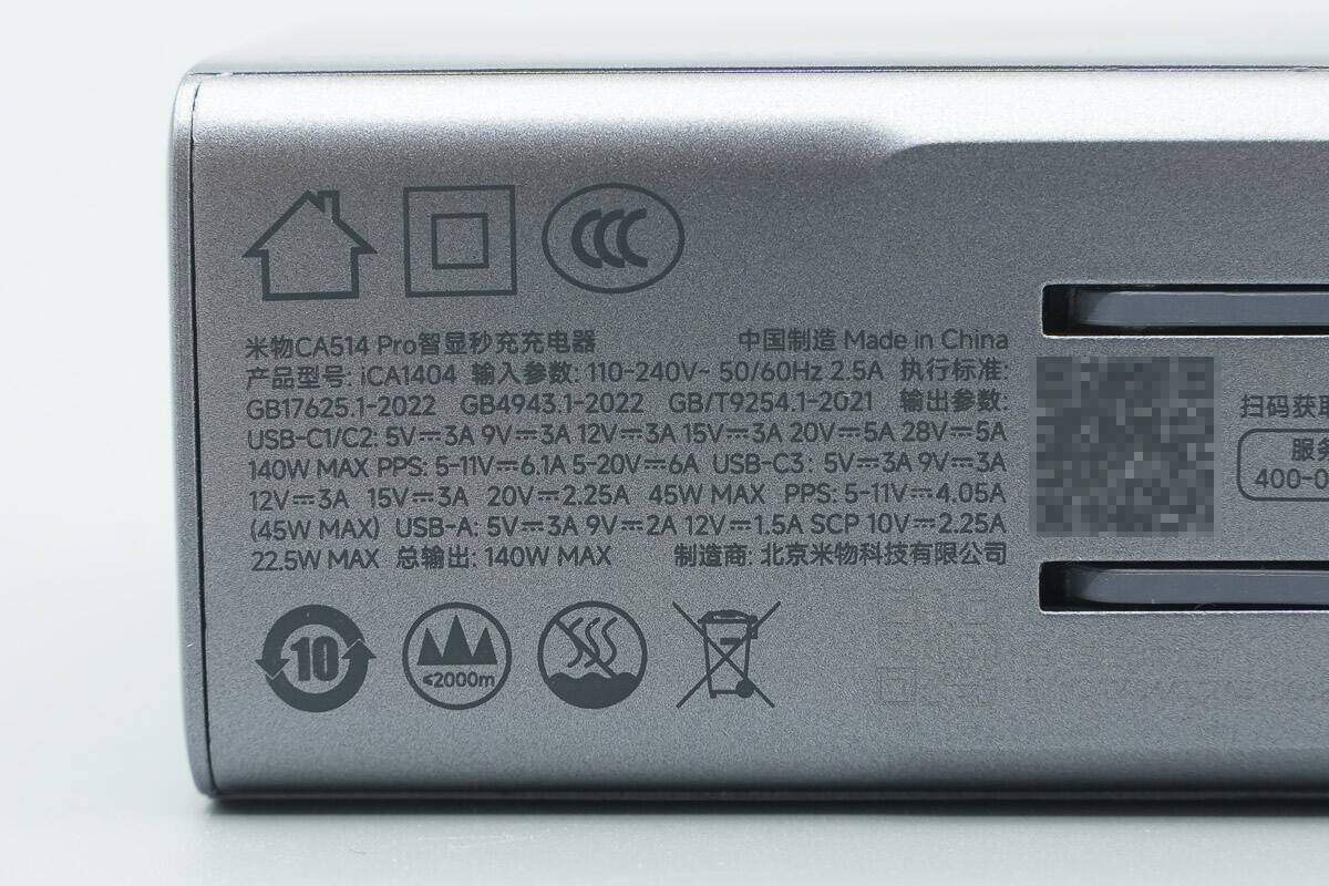
Model: iCA1404
Input: 110-240V~50/60Hz 2.5A
Output:
USB-C1/C2: 5V 3A, 9V 3A, 12V 3A, 15V 3A, 20V 5A, 28V 5A, 140W MAX
PPS: 5-11V 6.1A, 5-20V 6A
USB-C3: 5V 3A, 9V 3A, 12V 3A, 15V 3A, 20V 2.25A, 45W MAX
PPS: 5-11V 4.05A (45W MAX)
USB-A: 5V 3A, 9V 2A, 12V 1.5A, SCP 10V 2.25A, 22.5W MAX
Total Output: 140W MAX
The charger is CCC certified.
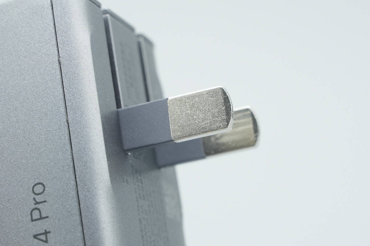
It comes with foldable plug prongs.
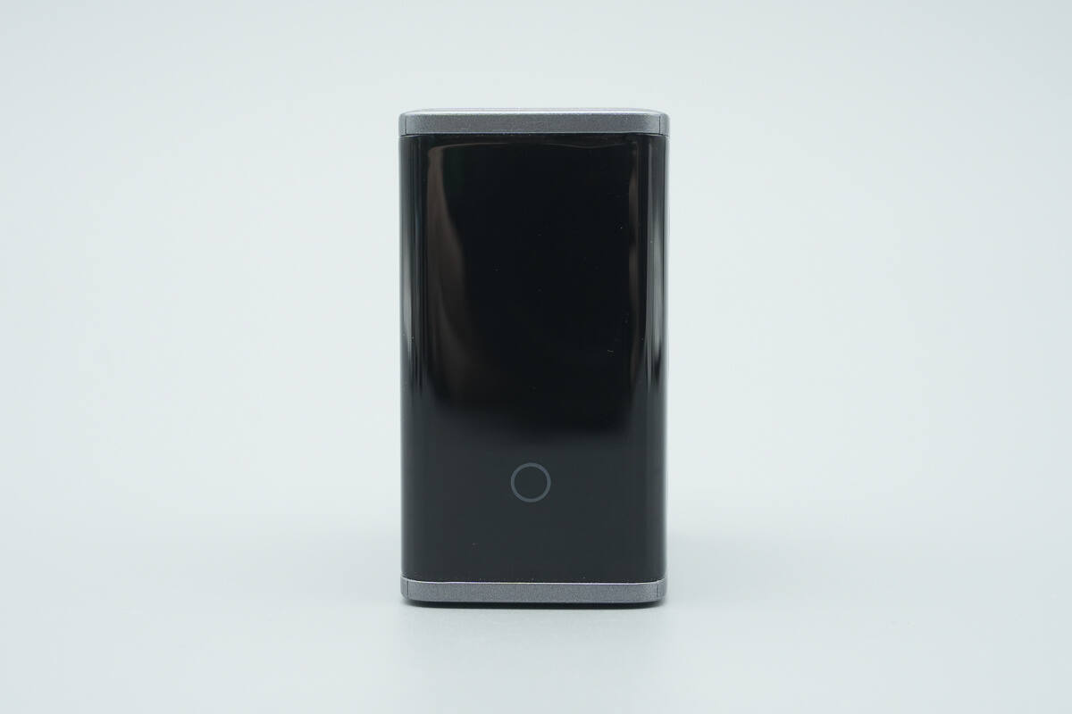
It features a TFT display with a borderless design on the top.
The interface can be switched using touch-sensitive buttons.

Long-pressing the touch button allows the screen to switch between landscape and portrait modes.
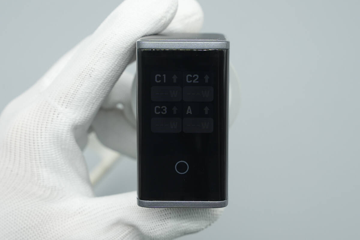
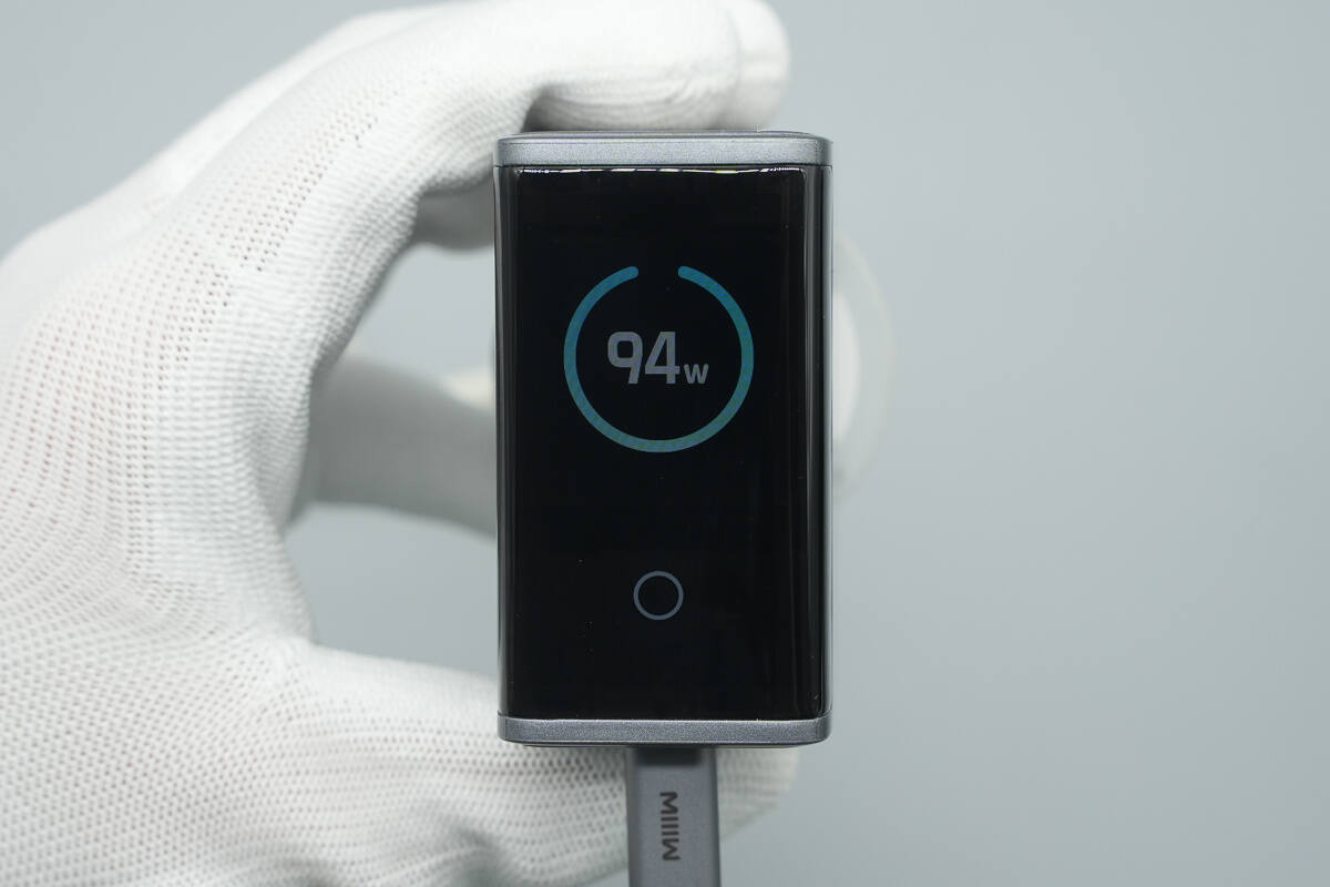
The multi-port power display interface shows the real-time output power of each individual port.

The charger uses a proprietary algorithm combined with a high-sensitivity NTC sensor to monitor temperature in real time. The temperature interface provides visible feedback, enhancing safety and giving users greater peace of mind.
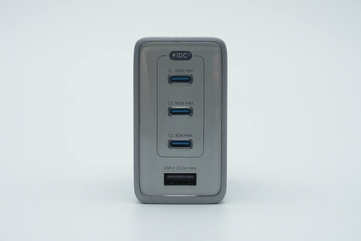
The output side is equipped with three USB-C ports and one USB-A port, with each port labeled with its respective maximum output power.
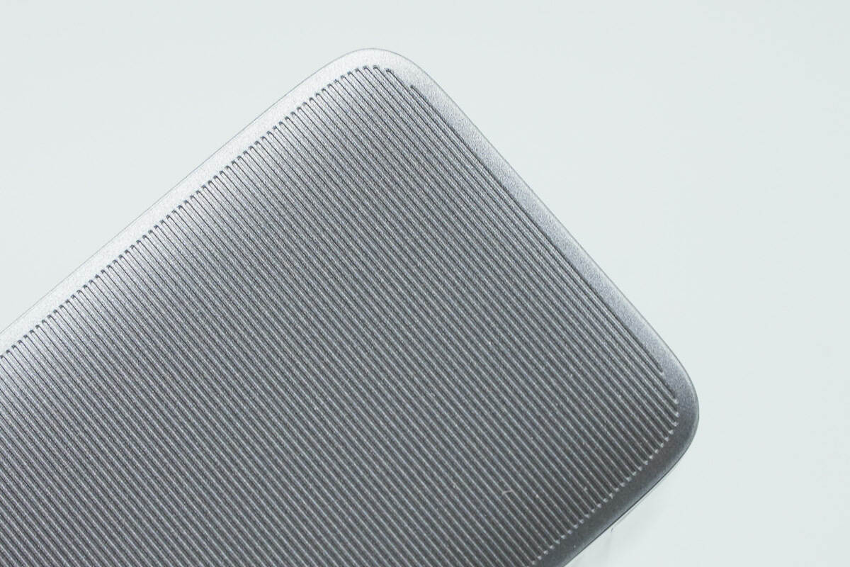
The opposite side of the enclosure features a textured surface.

The length of the charger is about 63.64 mm (2.51 inches).

The width is about 62.84 mm (2.47 inches).
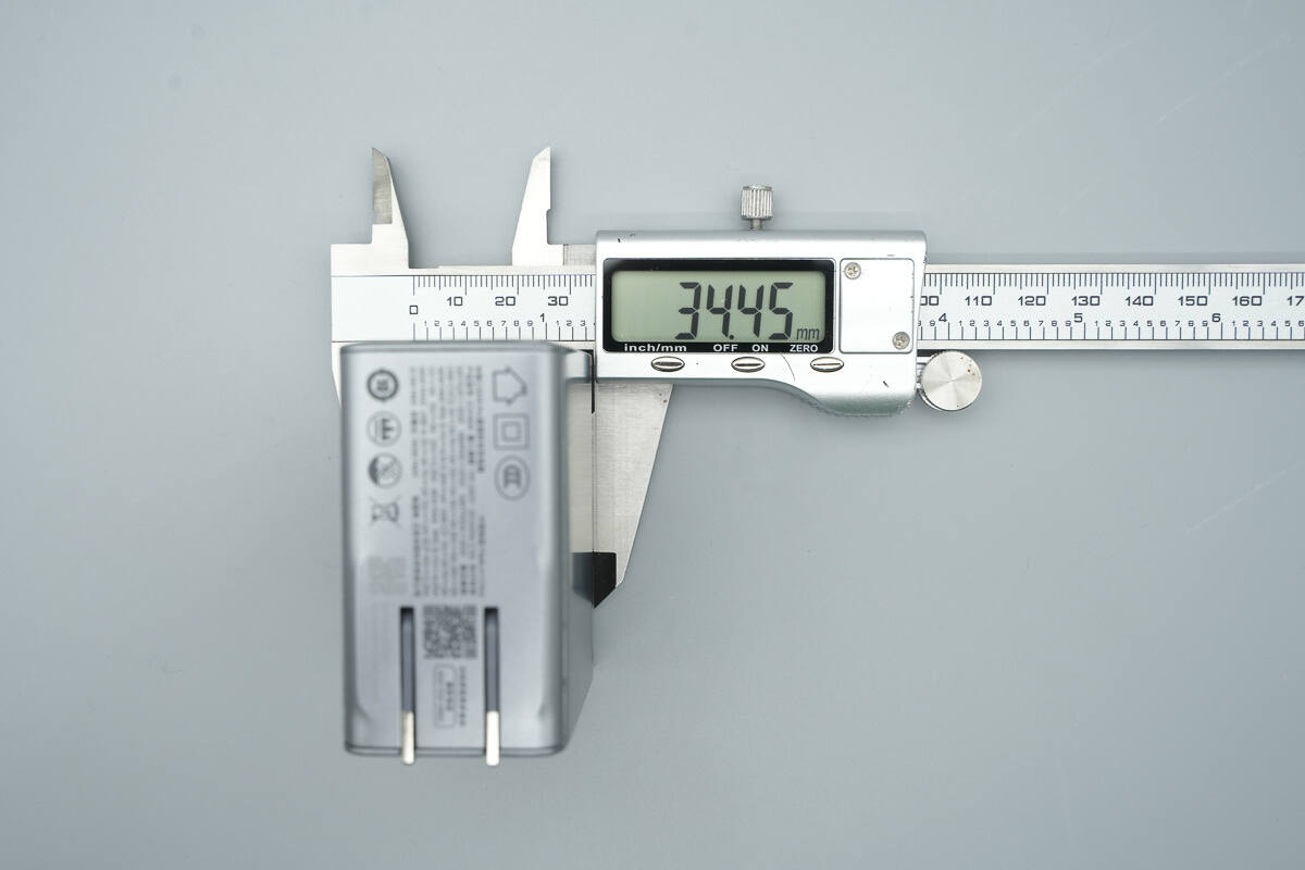
The thickness is about 34.45 mm (1.36 inches).
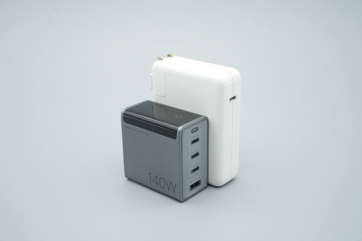
It is much smaller in size compared to the Apple 140W charger.
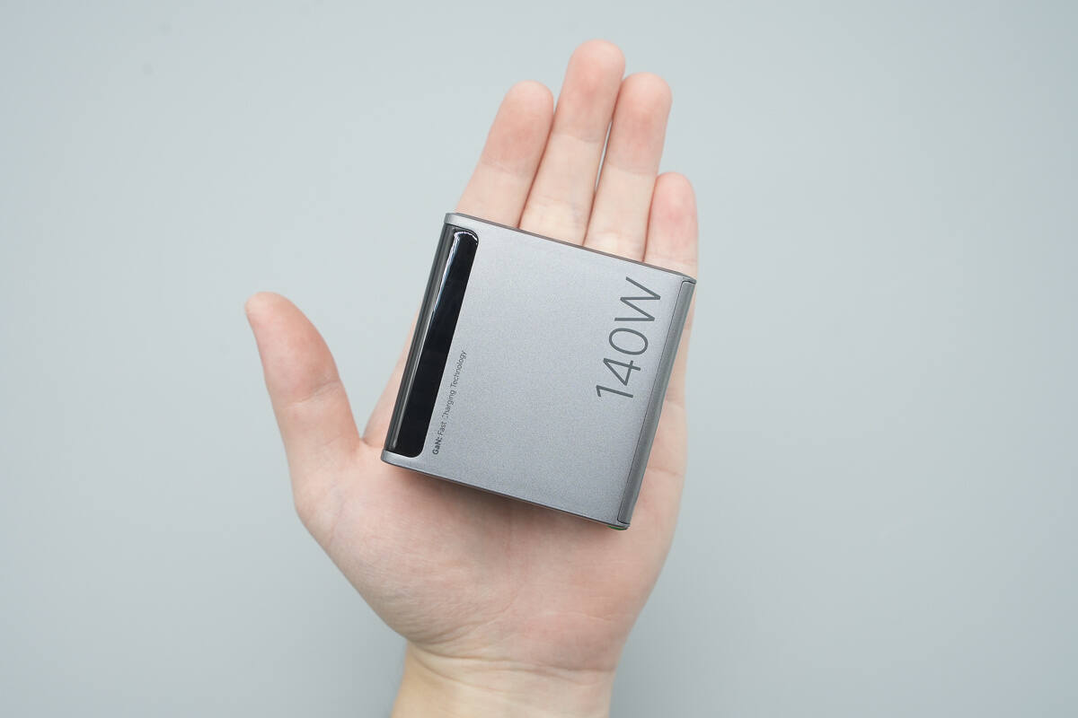
That's how big it is in the hand.
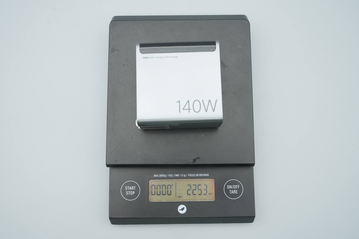
The weight is about 225 g (7.94 oz).
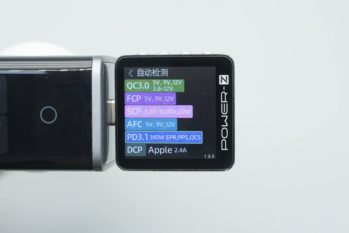
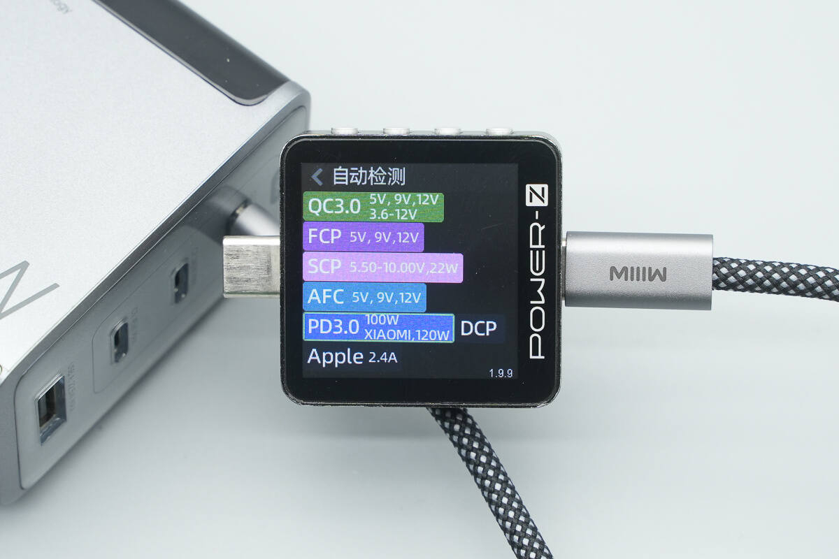
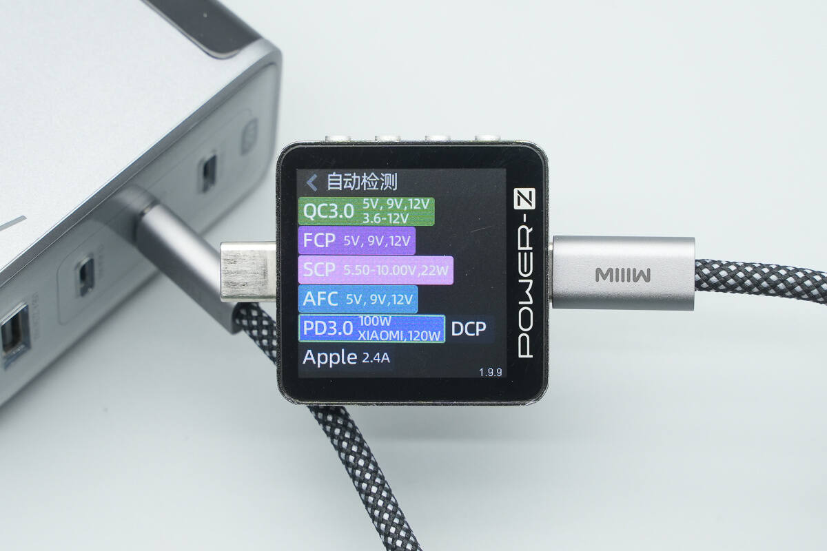
ChargerLAB POWER-Z KM003C shows that the USB-C1 supports QC3.0/5, FCP, SCP, AFC, PD3.1, PPS, DCP, and Apple 2.4A charging protocols.
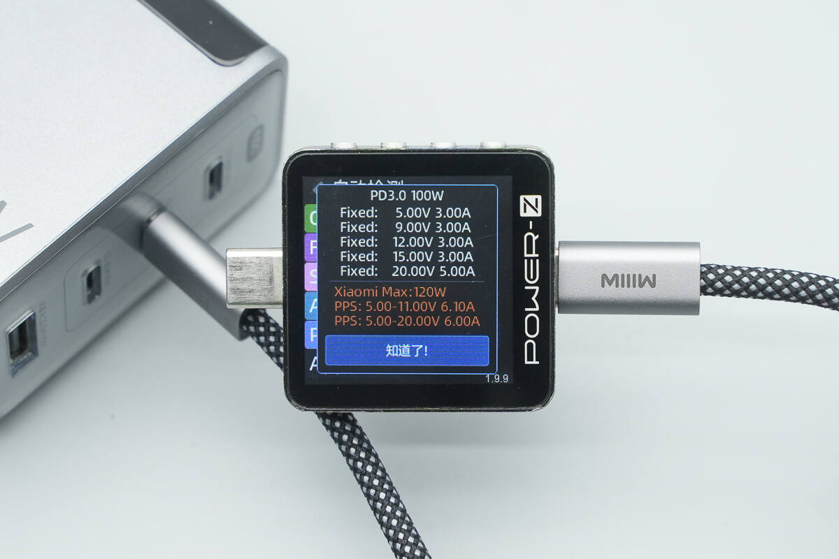
Testing confirmed support for Xiaomi’s 120W Surge fast charging.
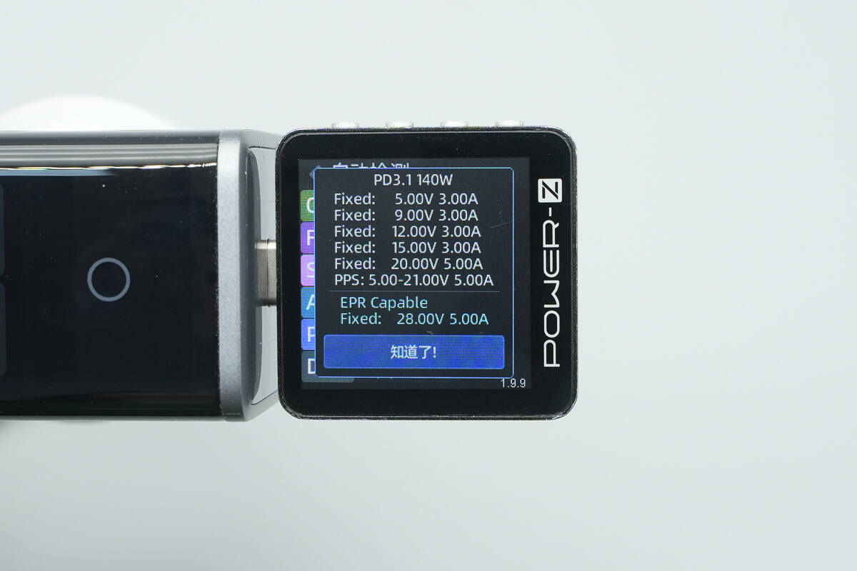
It features six fixed PDOs of 5V3A, 9V3A, 12V3A, 15V3A, 20V5A, and 28V5A. It also has one set PPS, which is 5-21V5A.
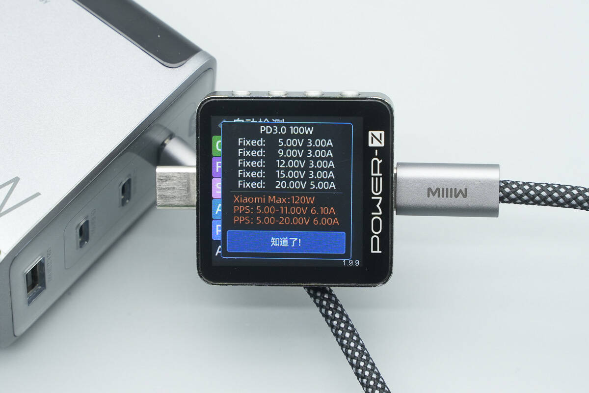
Testing confirmed that it supports two Xiaomi 120W Surge fast-charge private voltage levels: 5–11V 6.1A and 5–20V 6A.
The USB-C2 port supports the same protocols as the USB-C1 port.
It also supports Xiaomi’s 120W Surge fast charging.

The PDO report is identical to that of the USB-C1 port.
The USB-C2 port also supports two Xiaomi 120W Surge fast-charge levels: 5–11V 6.1A and 5–20V 6A.
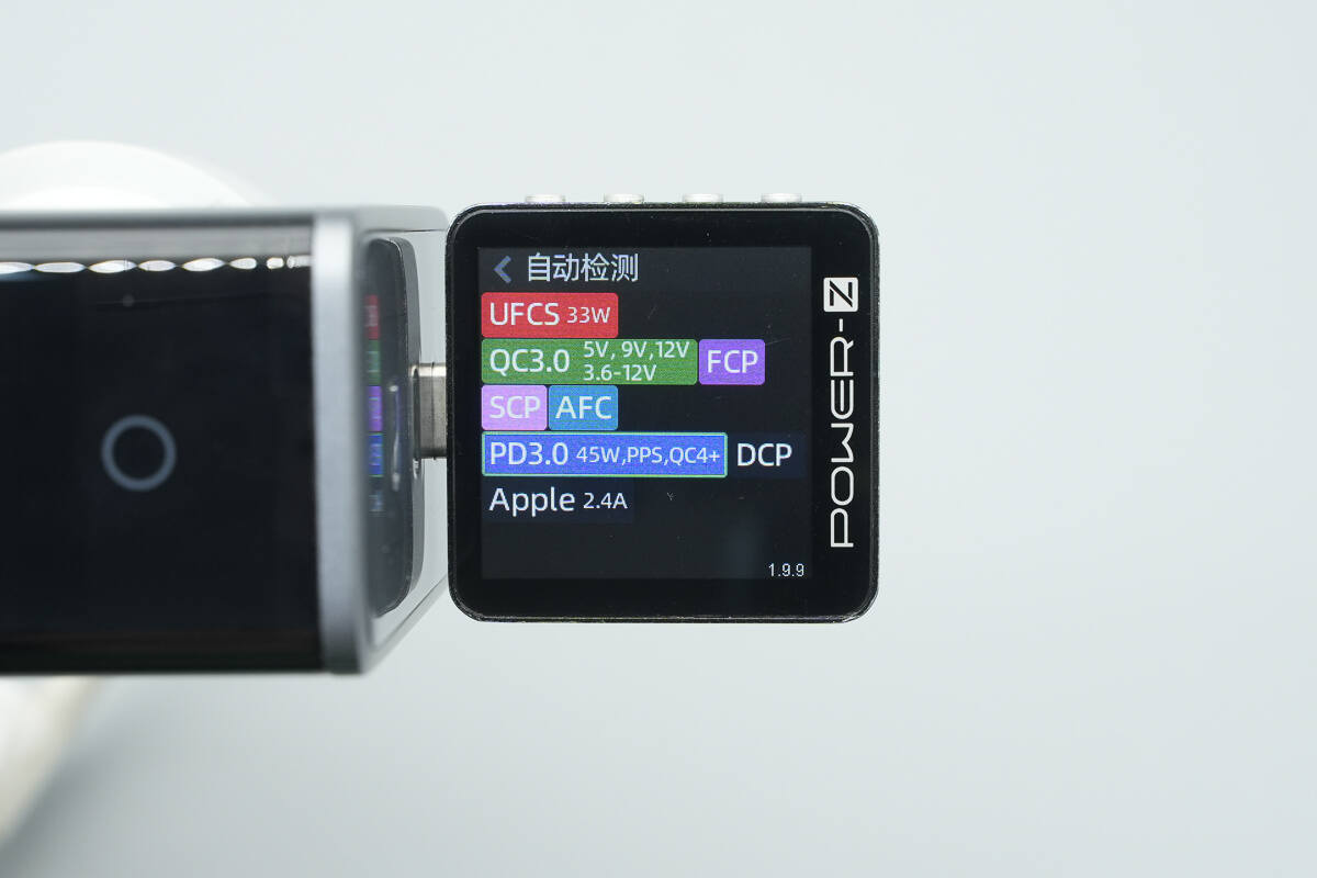
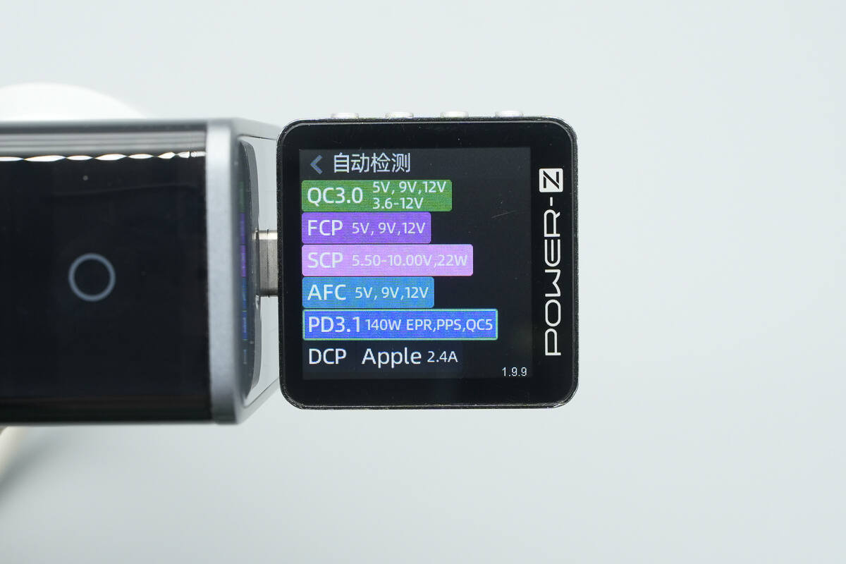
The USB-C3 supports UFCS, QC3.0, FCP, SCP, AFC, PD3.0, PPS, DCP, and Apple 2.4A charging protocols.
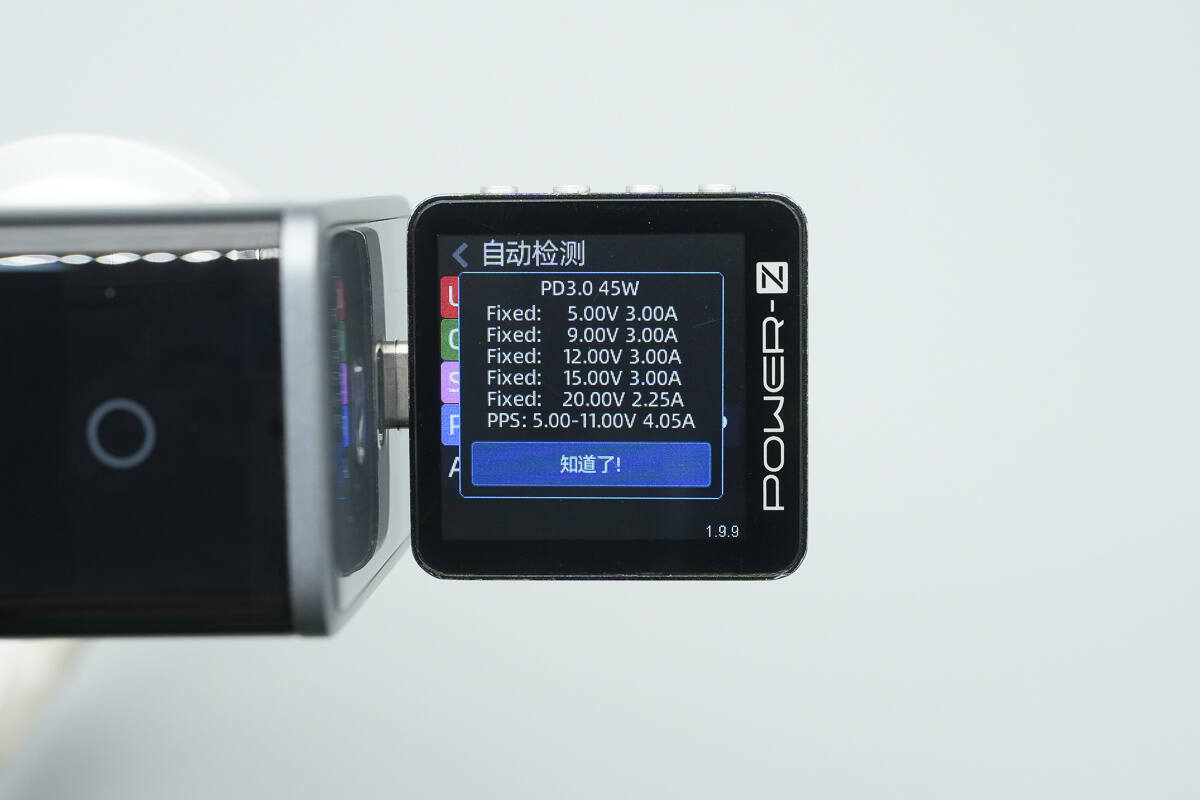
It features five fixed PDOs of 5V3A, 9V3A, 12V3A, 15V3A, and 20V2.25A. It also has one set PPS, which is 5-11V4.05A.

The USB-A supports UFCS, QC3.0, FCP, SCP, AFC, DCP, and Apple 2.4A charging protocols.
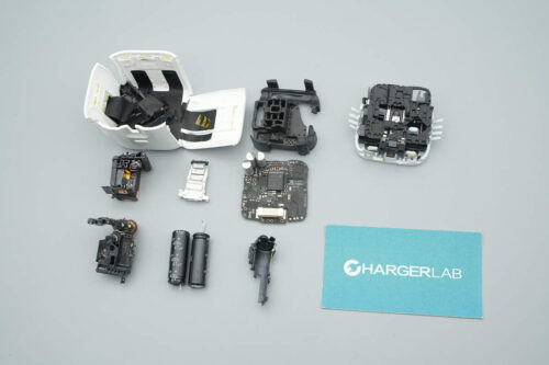
Teardown
Next, let's take it apart to see its internal components and structure.
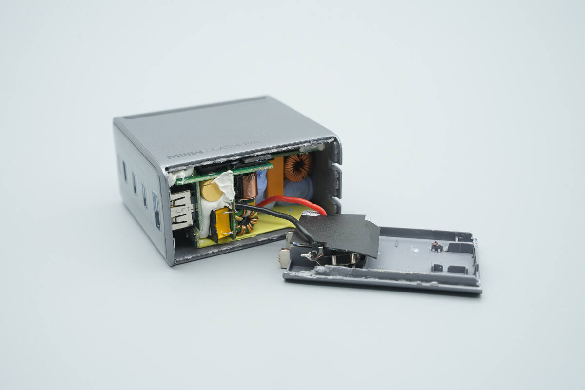
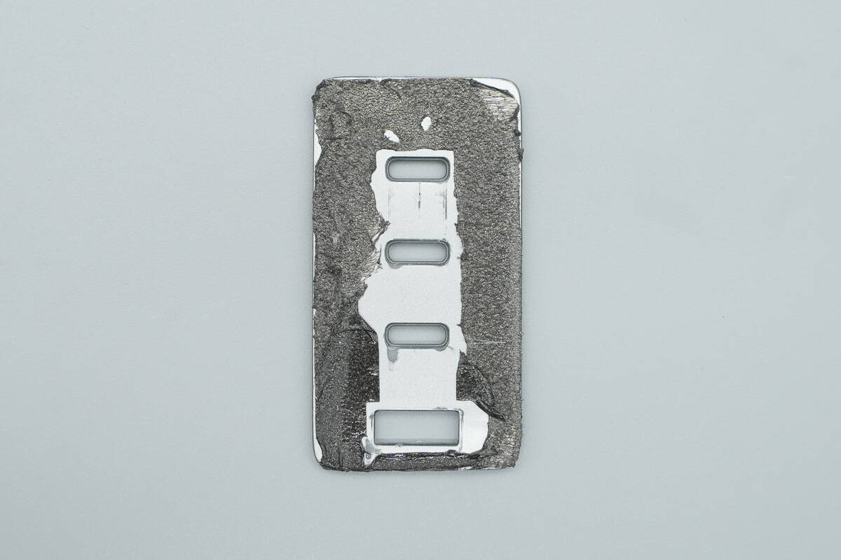
Open the bottom case. The plug prongs are connected to the PCBA module via wires. The prongs are covered with a Mylar sheet for insulation.

After removing the screen and the output panel, the PCBA module can be taken out.
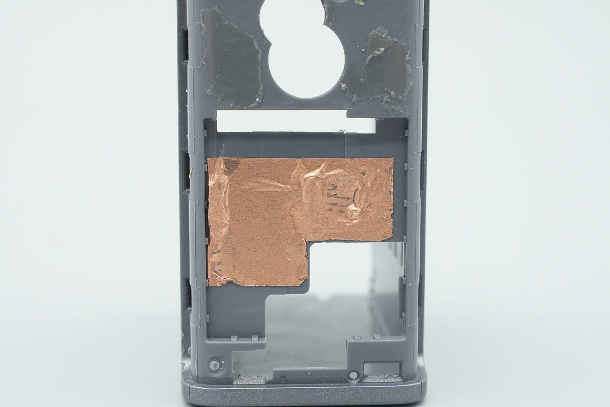
Copper foil is attached inside the groove corresponding to the screen.

The screen is secured with foam adhesive and connected to the PCBA module via a flexible flat cable.
The output panel is also secured using foam adhesive.
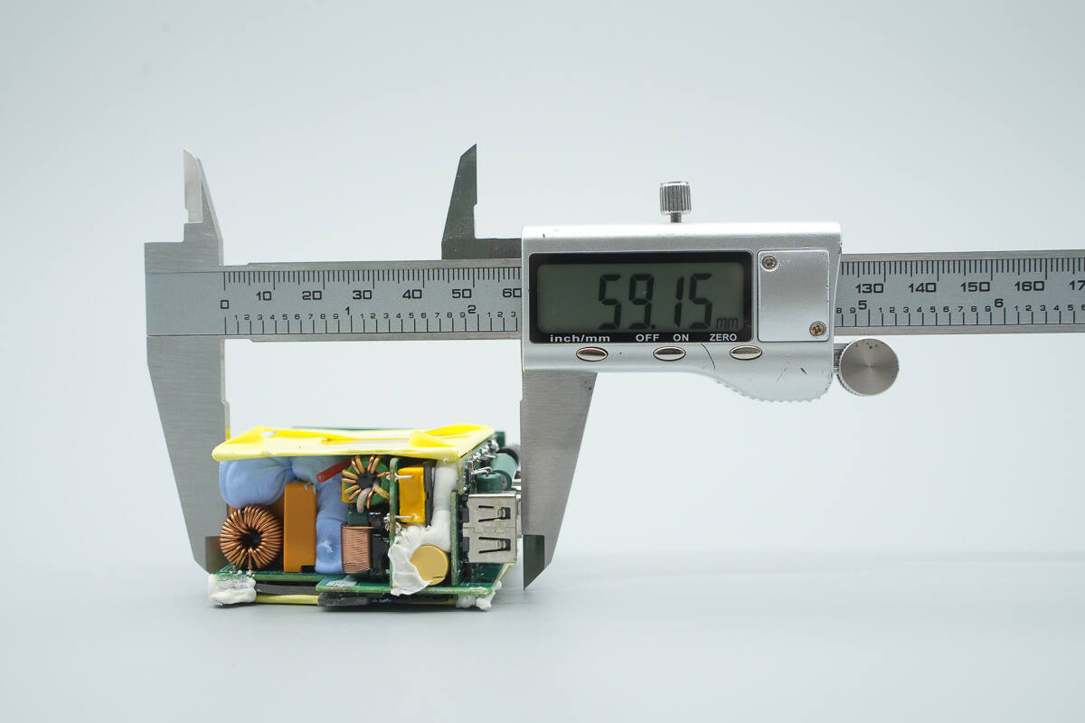
The length of the PCBA module is about 59.15 mm (2.33 inches).

The width is about 57.33 mm (2.26 inches).
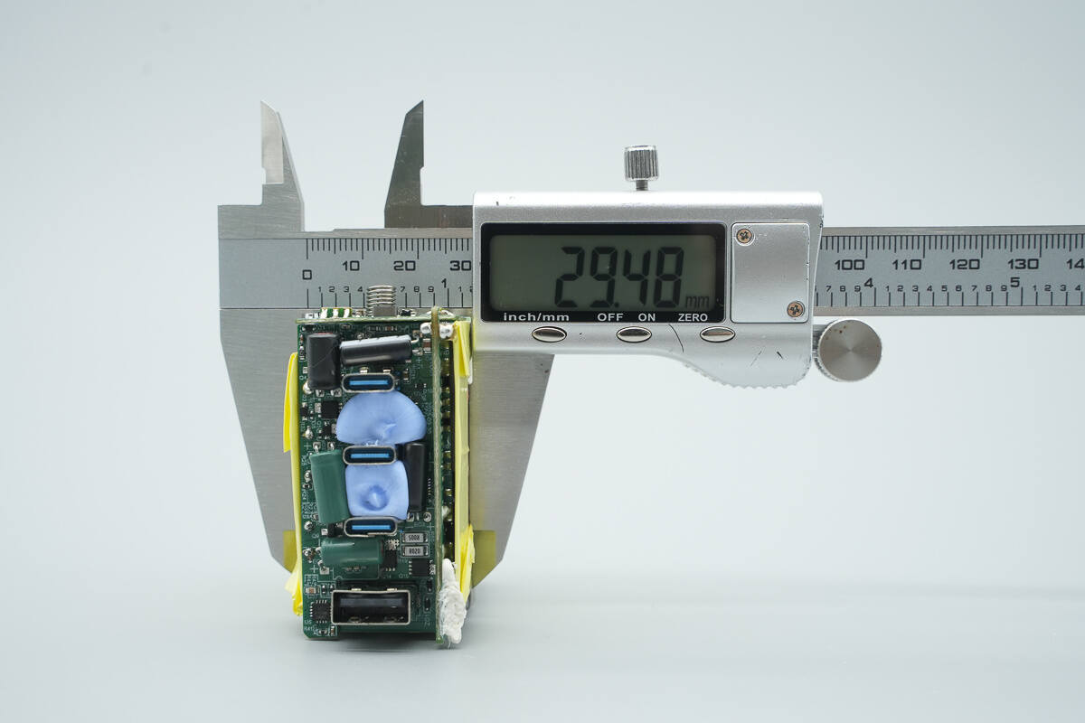
The thickness is about 29.48 mm (1.16 inches).
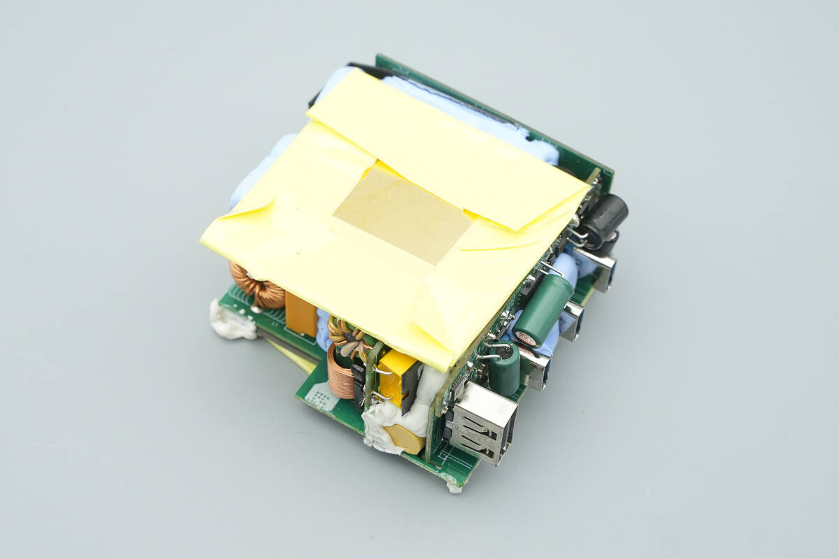
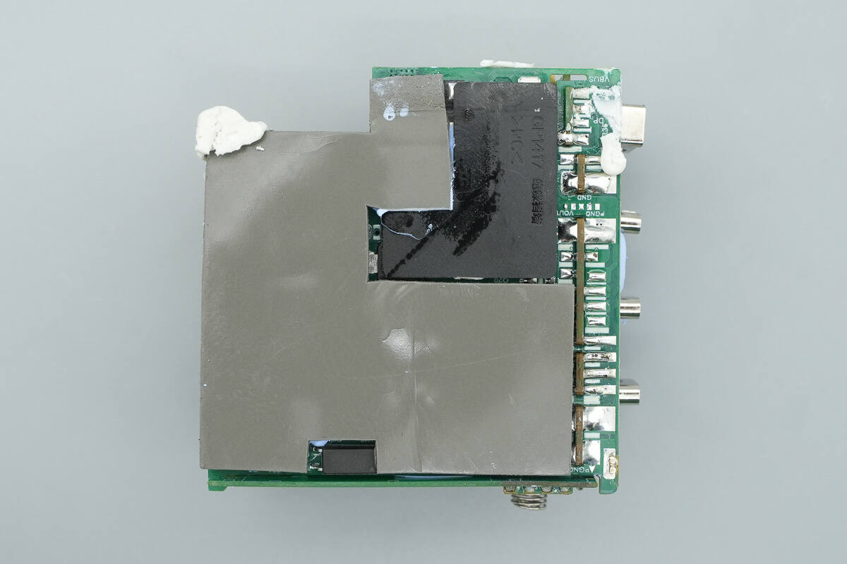
The top of the PCBA module is covered with a heatsink and wrapped with adhesive tape.
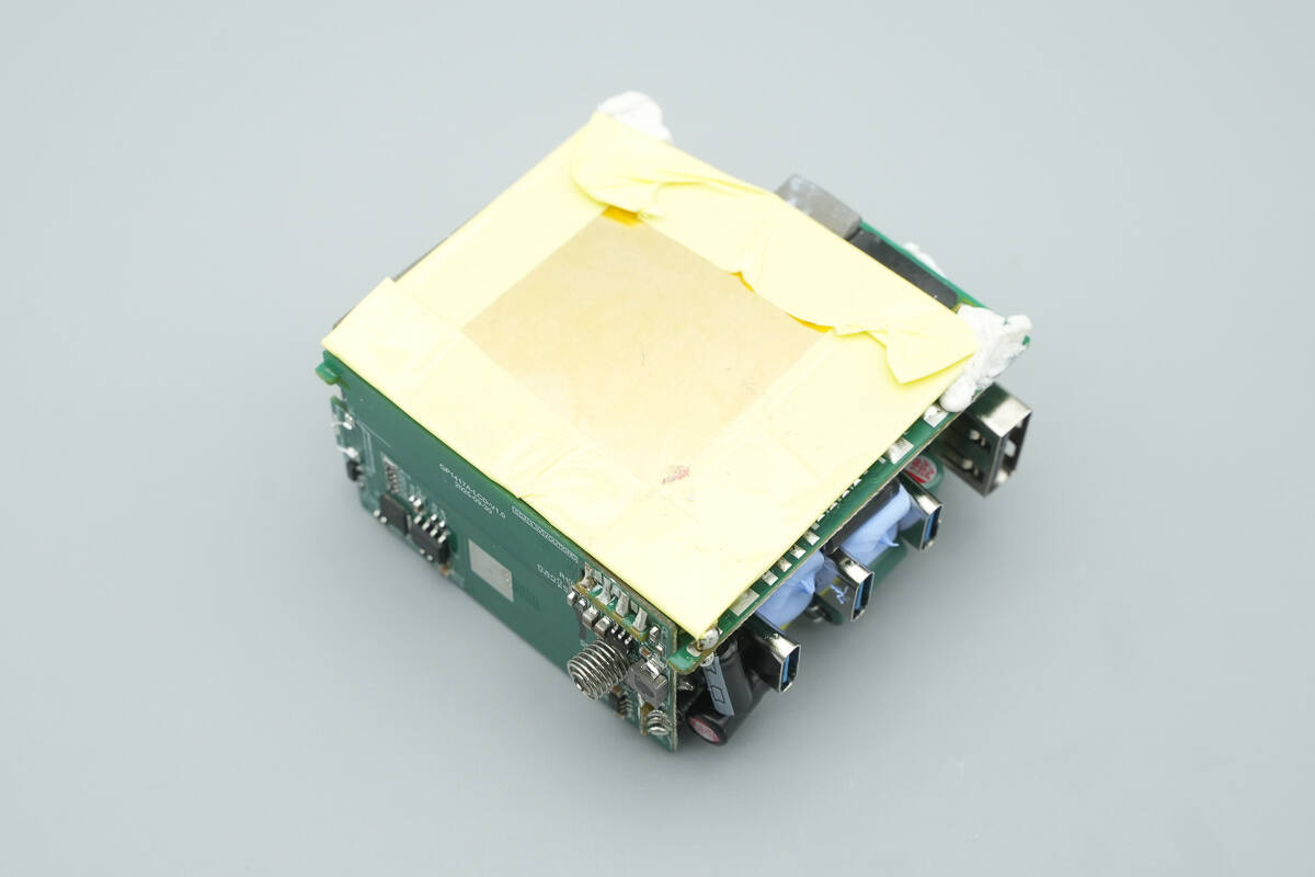
The bottom is also covered with a heatsink.
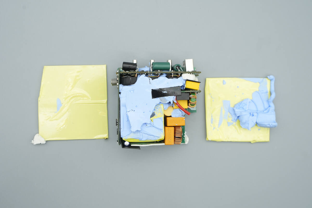
Remove the heatsinks. The module is reinforced with potting compound, which also aids in heat dissipation.
The bottom is additionally covered with a plastic plate and a thermal pad.

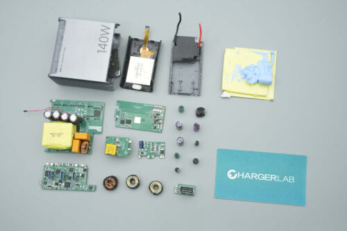
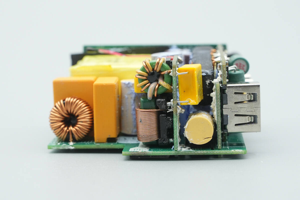
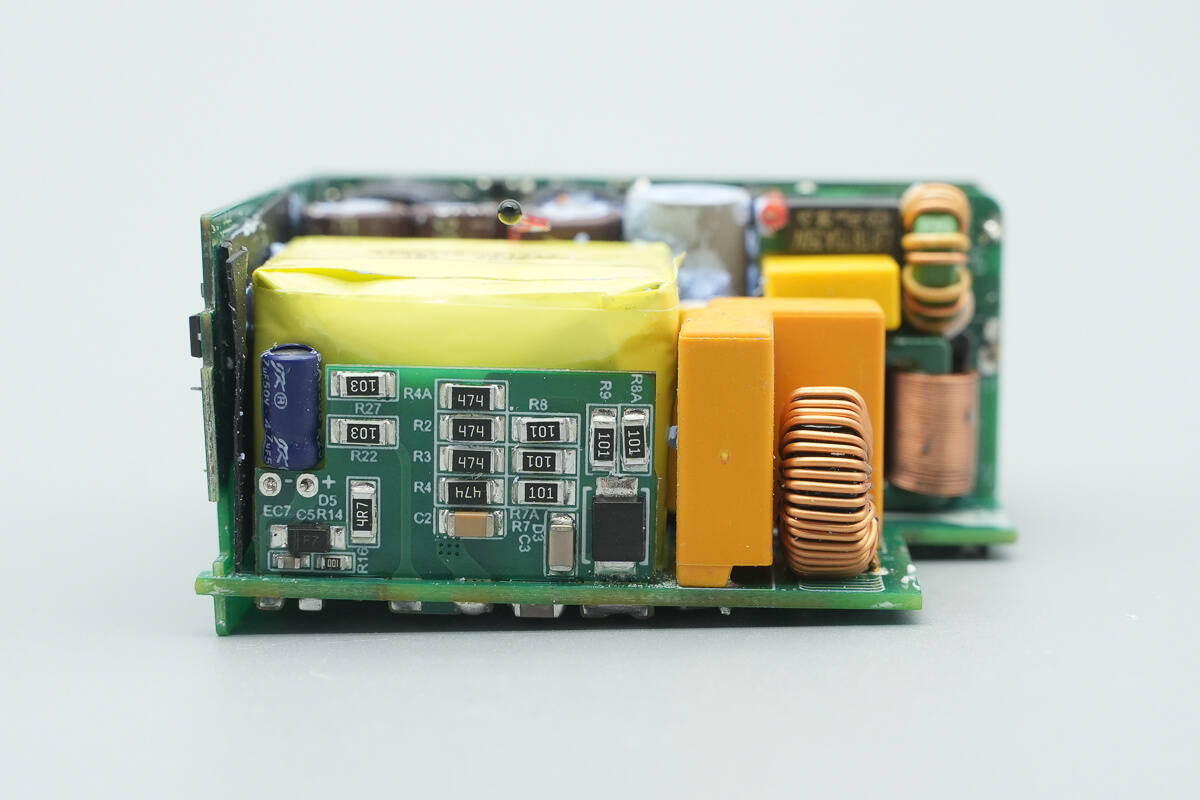
After cleaning the module, it is revealed that the PCBA module features a stacked design with six small PCBs. The component layout on the front side is compact.
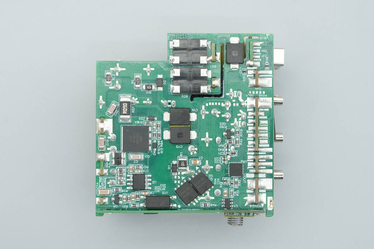
The back side features components such as bridge rectifiers, the master control chip, a primary MOSFET, a synchronous rectifier controller, synchronous rectifiers, and an MCU.
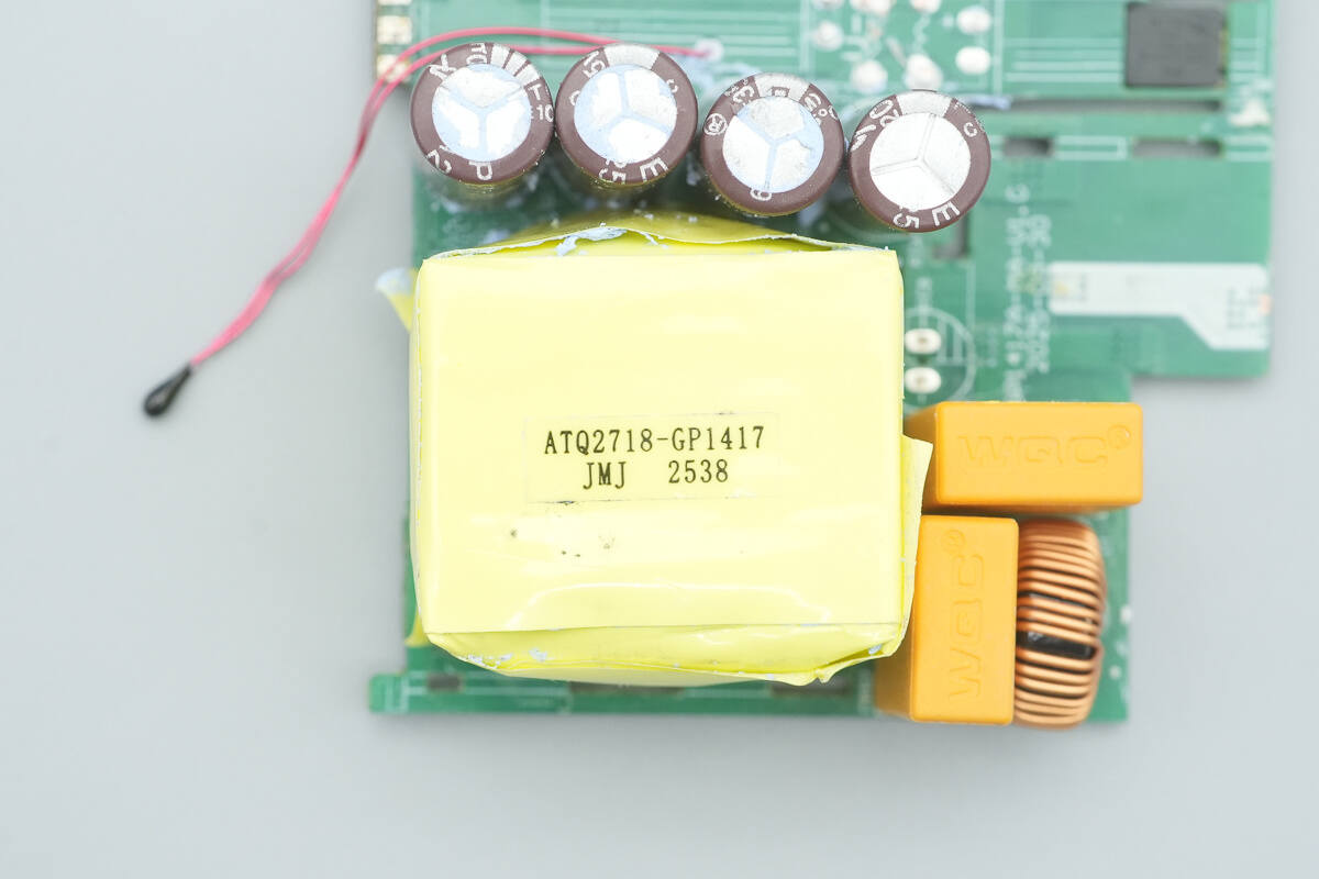
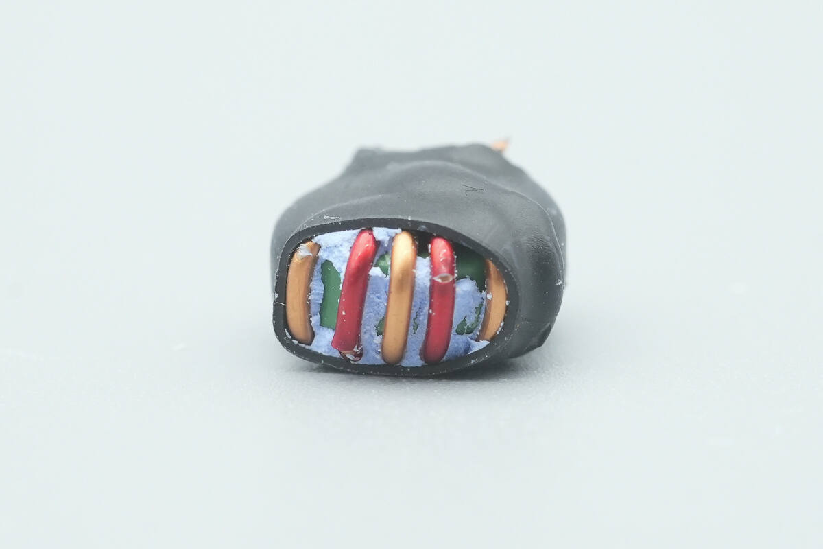
A view of the input side shows that the electrolytic capacitor at the center is covered with a yellow insulating sleeve.

Remove the input PCB. The front side reveals a time-delay fuse, common mode chokes, and a safety X2 capacitor.
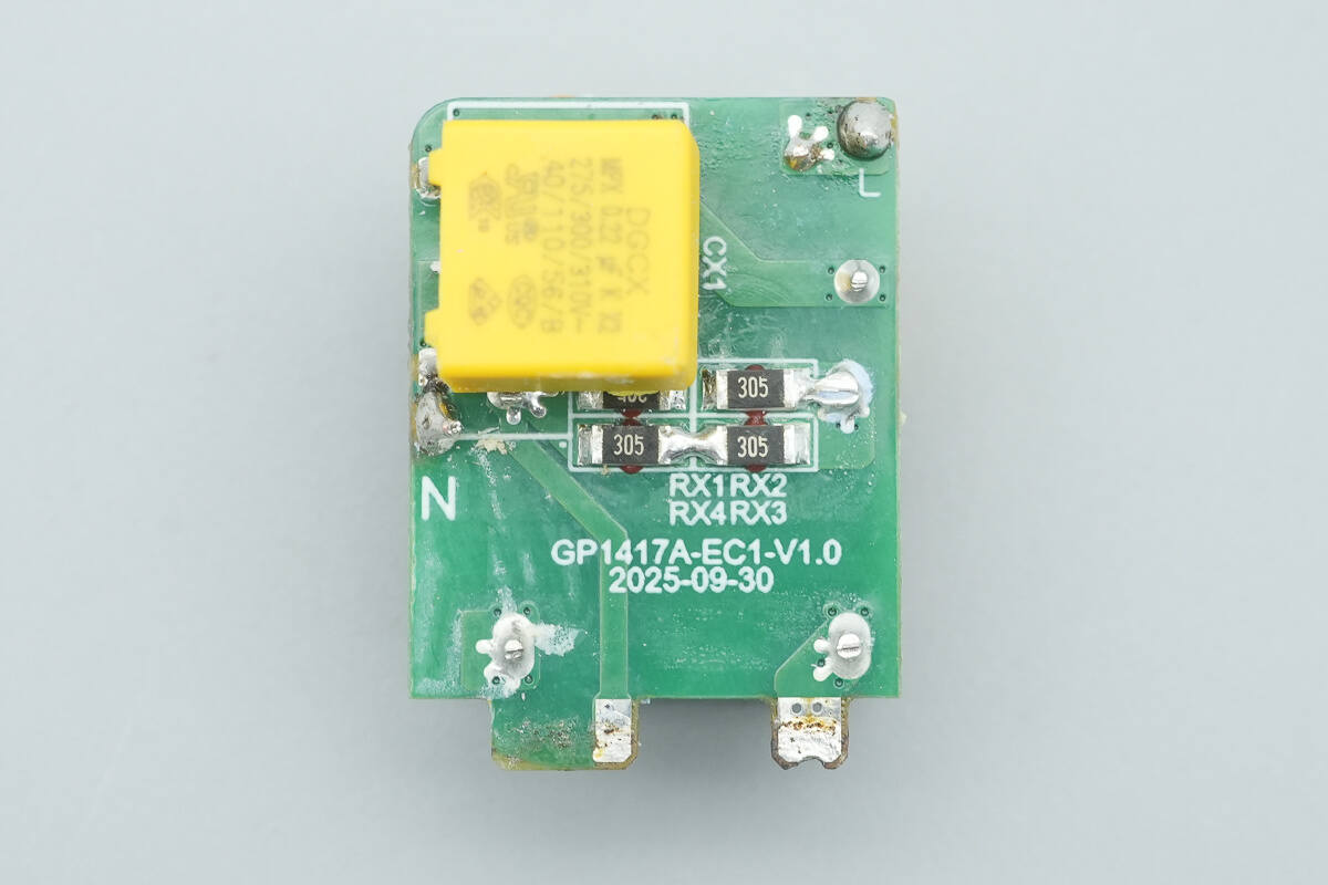
The back side features a safety X2 capacitor.
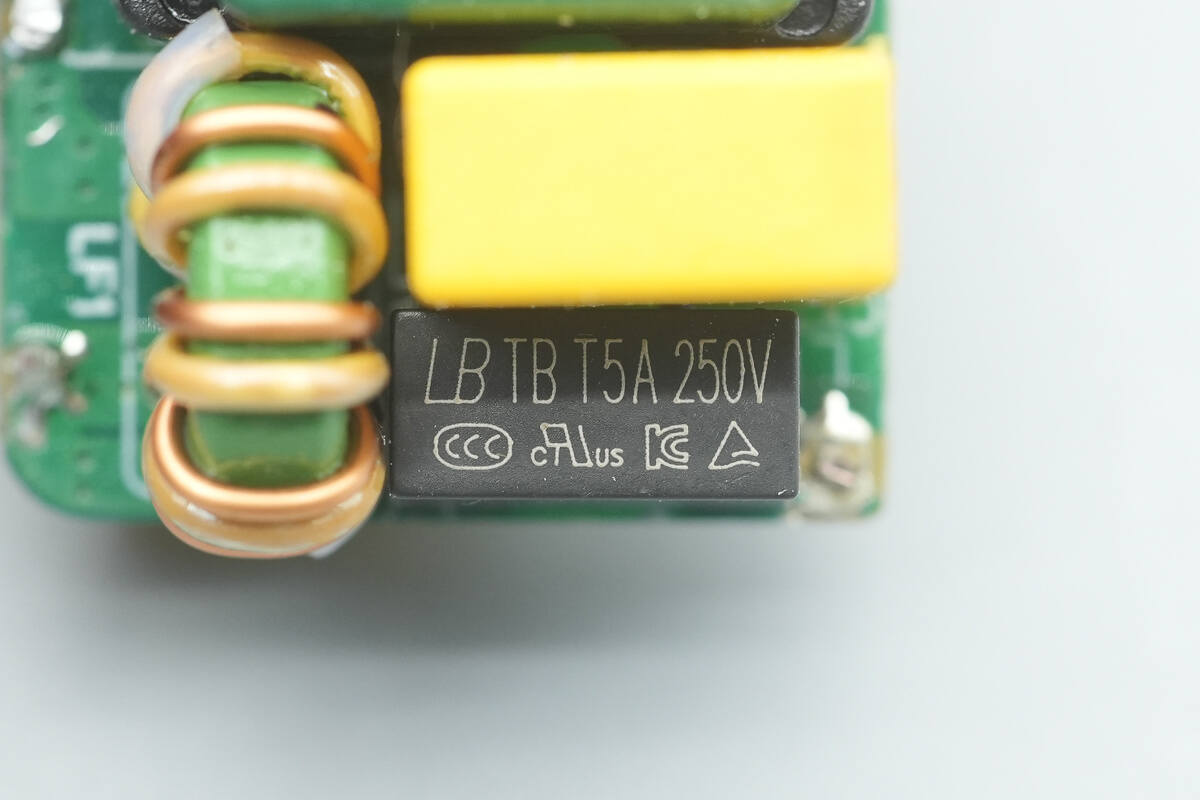
The time-delay fuse is from Lanbao, rated at 5A 250V.
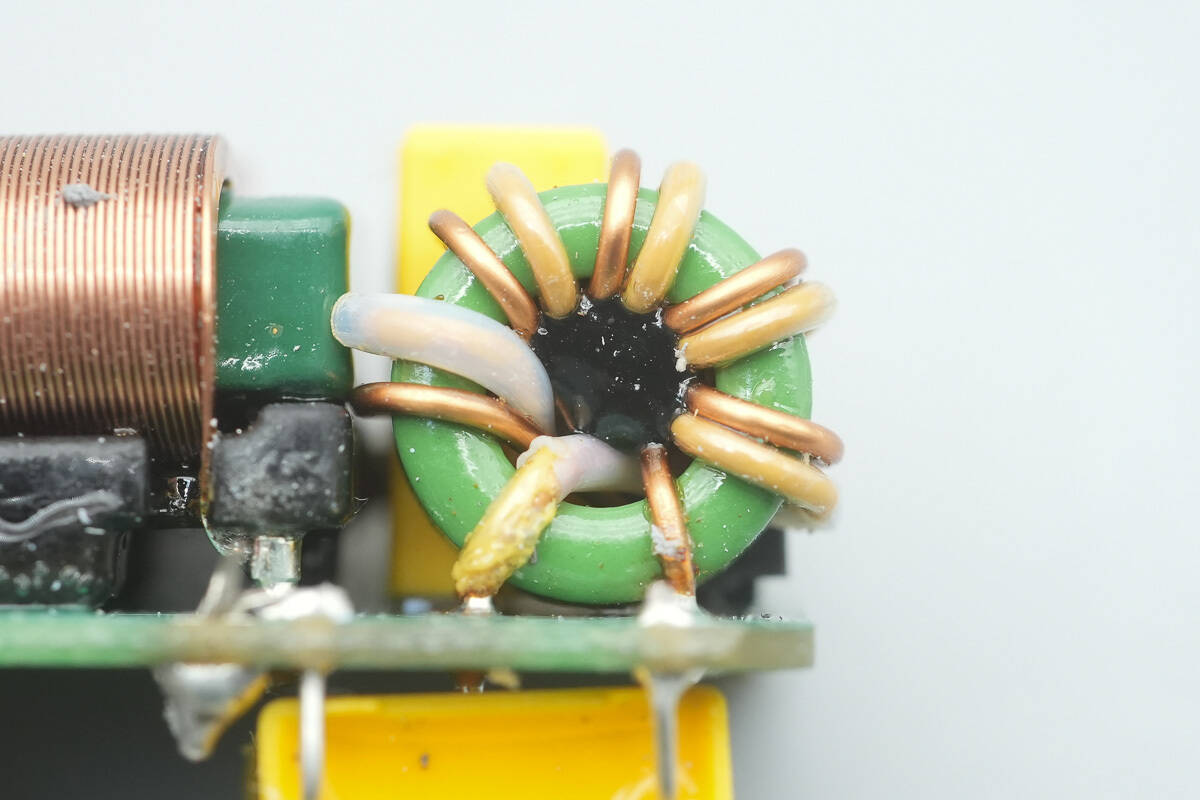
The common mode choke is used to filter out EMI interference.
Close-up of the other common mode choke.
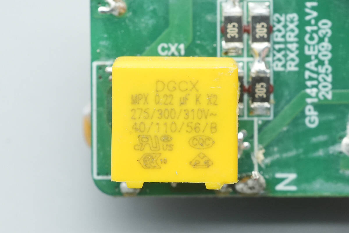
The safety X2 capacitor is from DGCX with a capacitance of 0.22 μF.

The bridge rectifiers marked with R8M are from ZOWIE and use two units to share heat dissipation.
A small PCB is soldered on this side of the module, with a Mylar sheet placed between it and the transformer.

After removing the small PCB, the back side reveals a capacitor that supplies power to the master control chip.

The two yellow film capacitors are from WQC, part of the MPC series boxed capacitors, rated at 1 μF 450 V.
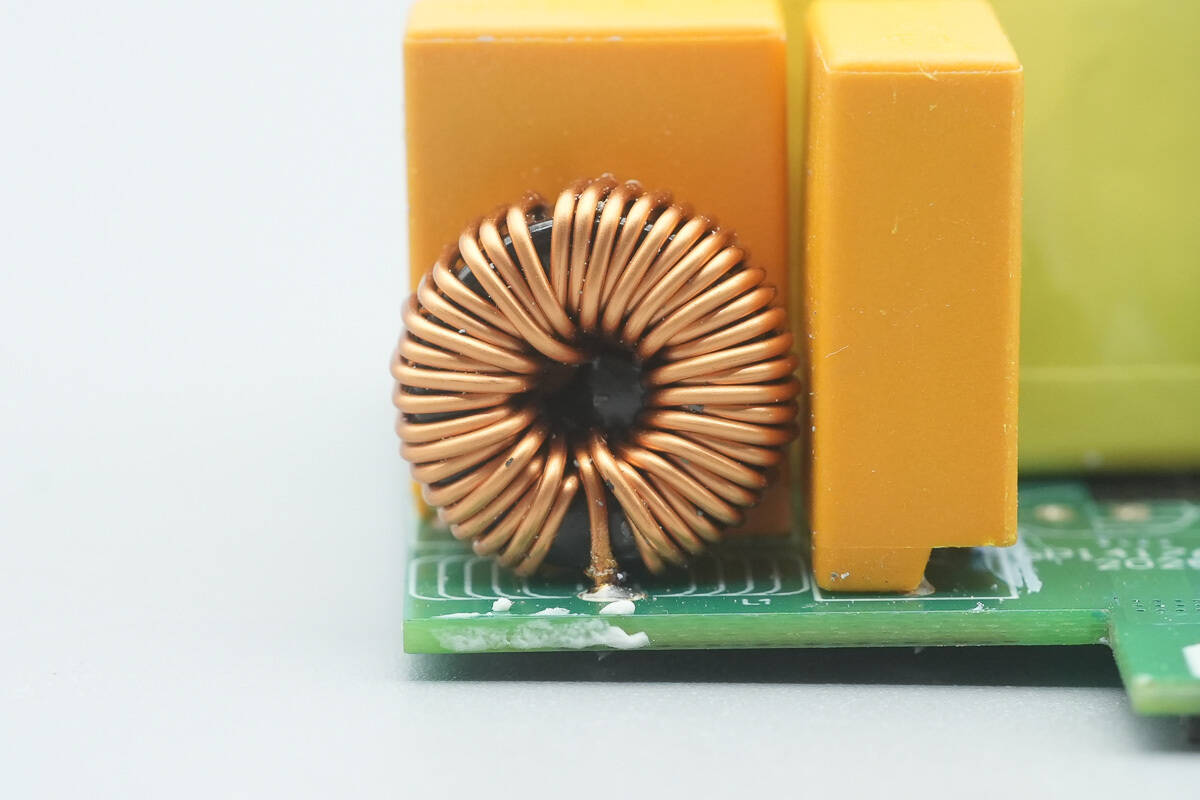
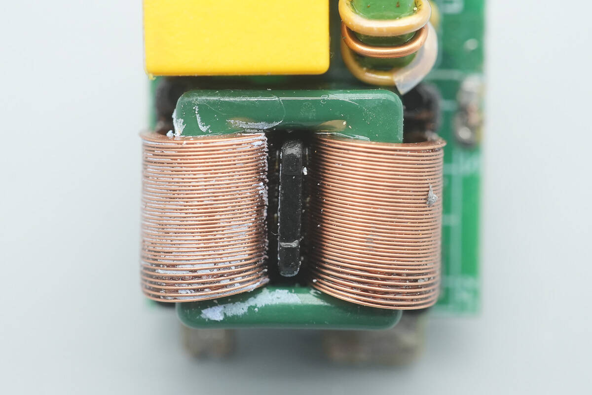
Close-up of the filter inductor.

The high-voltage electrolytic capacitor is from JK, rated at 400 V, 10 μF.

The master control chip is from Kiwi Instruments, model KP2815. It is a primary-side feedback high-PF flyback constant-voltage controller. The chip operates in quasi-resonant valley-turn-on mode, offering high efficiency and excellent EMC performance. It integrates a high power factor algorithm and THD compensation, achieving PF > 0.95 and THD < 10% across the full voltage range, while also meeting low-load harmonic requirements.
The KP2815 employs primary-side feedback for constant-voltage (CV) and constant-current (CC) control. Under normal load conditions, it operates in CV mode: the chip samples the output voltage via the auxiliary winding in real time, regulating the output to match the reference voltage with ±3% accuracy. Under overload conditions, it switches to CC mode: by sampling the voltage across the primary-side sense resistor, the built-in high-precision CC control algorithm maintains a constant output current with ±7% accuracy.

The KP2815 integrates an adaptive, high-sensitivity, fast dynamic response mechanism, keeping output voltage overshoot and drop within a minimal range during load transients. It also features adaptive input voltage detection and a frequency-sweeping function under DC input, which lowers switching-frequency noise and allows for smaller input filter components.
The KP2815 includes comprehensive protection features to ensure safe and reliable operation, such as input overvoltage/undervoltage protection, cycle-by-cycle overcurrent protection, over-temperature protection, AOCP protection during startup and short-circuit conditions, output overvoltage protection, and output short-circuit protection.
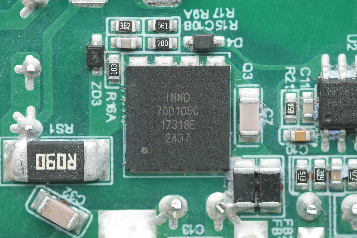
The primary MOSFET is from Innoscience, model INN700D105C. It is a 700 V enhancement-mode GaN transistor with an on-resistance of 105 mΩ. The device supports ultra-high switching frequencies, has zero reverse-recovery charge, and features very low gate and output capacitances. It meets JEDEC industrial application standards, includes built-in ESD protection, and complies with RoHS, lead-free, and EU REACH regulations. It is suitable for high-efficiency, high-density applications such as AC-DC and DC-DC conversion and comes in a DFN 8×8 package.
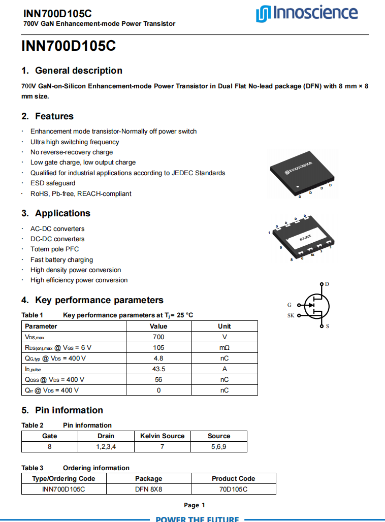
Here is the information about Innoscience INN700D105C.
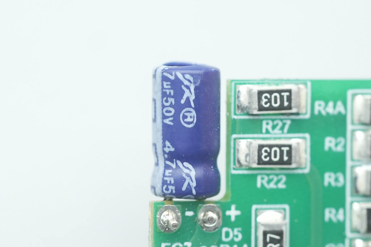
The capacitor supplying power to the master control chip is from JK, rated at 50 V, 4.7 μF.
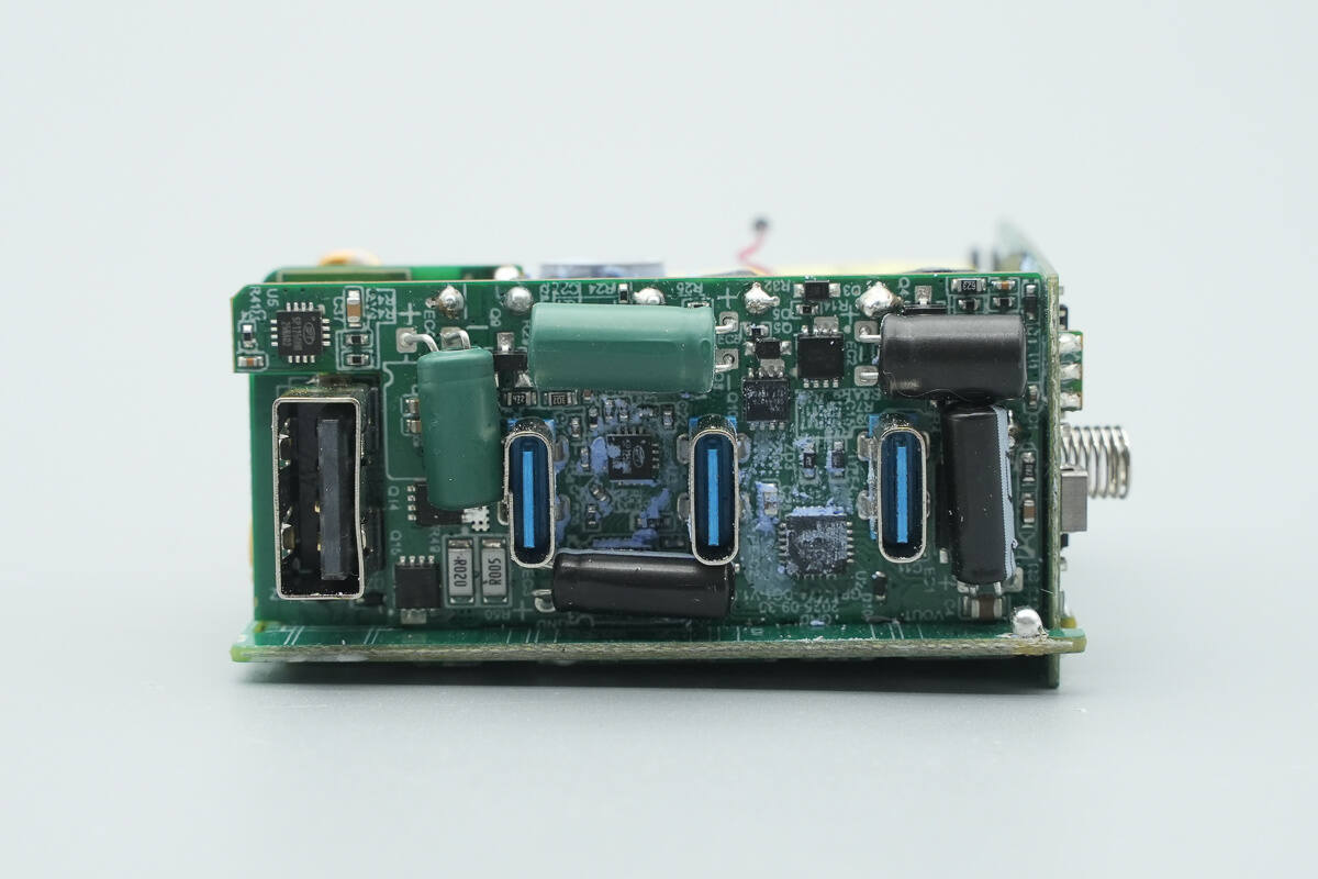
The USB-C ports are soldered onto the output PCB, while the USB-A port is mounted on a separate PCB.
A screen control PCB is soldered on the opposite side.
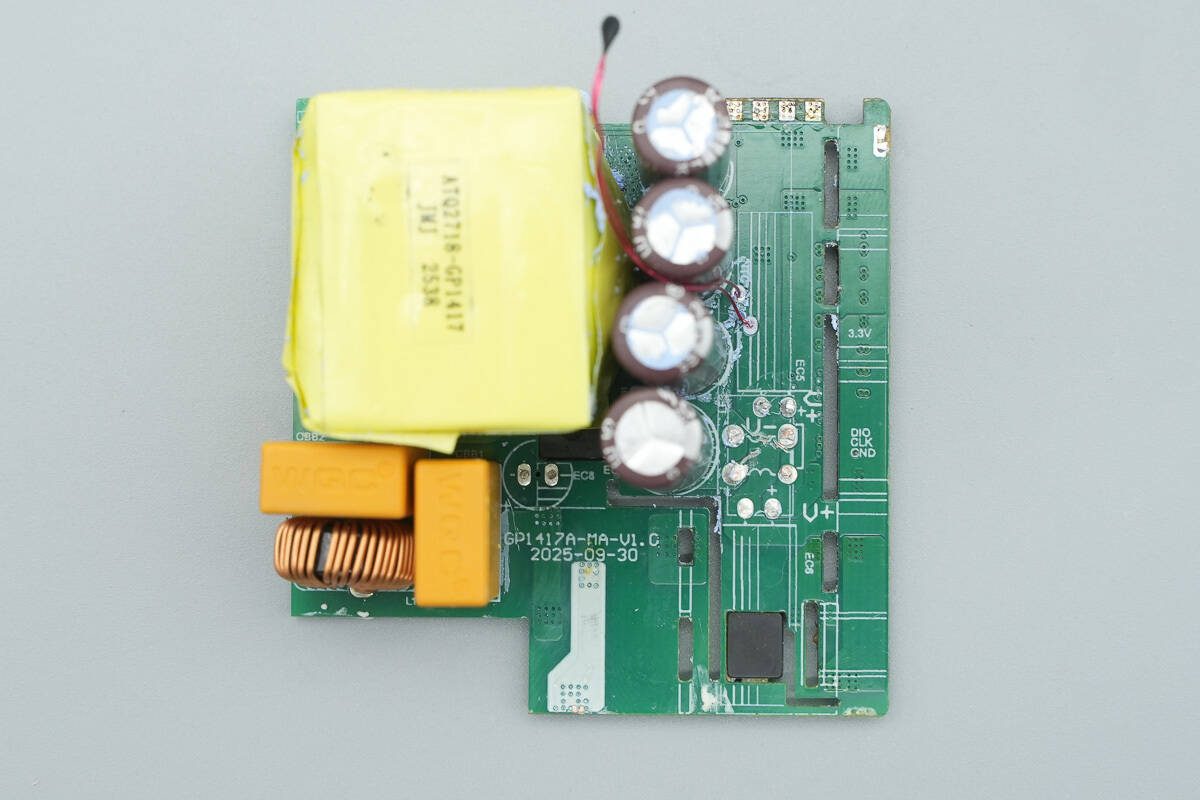
After removing all the small PCBs, the front side of the main board still has the transformer, electrolytic capacitors for output filtering, and a thermistor.
Close-up of the transformer.
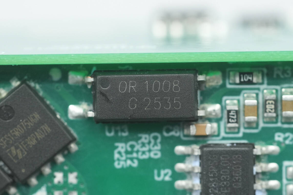
The OR1008 optocoupler is used for output voltage feedback.

The two SMD Y capacitors are from KeiFat.

The third SMD Y-capacitor is also from KeiFat.

The synchronous rectifier controller is from Kiwi Instruments, model KP4060, marked with M60. It supports DCM, CCM, and QR operating modes as well as active-clamp flyback topology, with a maximum switching frequency of 600 kHz. The chip integrates high-voltage detection and high-voltage power circuits, as well as an intelligent dual LDO, eliminating the need for auxiliary winding power. It also supports SR operation during output short circuits and comes in a space-saving SOT23-6 package.
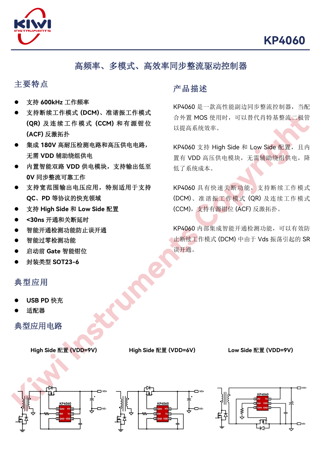
The KP4060 supports a wide range of output voltages, making it particularly suitable for fast-charging applications that support protocols like QC and PD. It can be configured for either high-side or low-side operation. With turn-on and turn-off delays of less than 30 ns and gate-drive clamping technology, it prevents false triggering caused by parasitic coupling. The chip also features patented intelligent current zero-cross turn-off and smart turn-on detection technologies to prevent misfiring, ensuring safe operation.

The synchronous rectifiers are from Oriental, model SFS15R075UGNF. They are NMOS transistors with a voltage rating of 150 V and an on-resistance of 8 mΩ, packaged in PDFN 5×6.
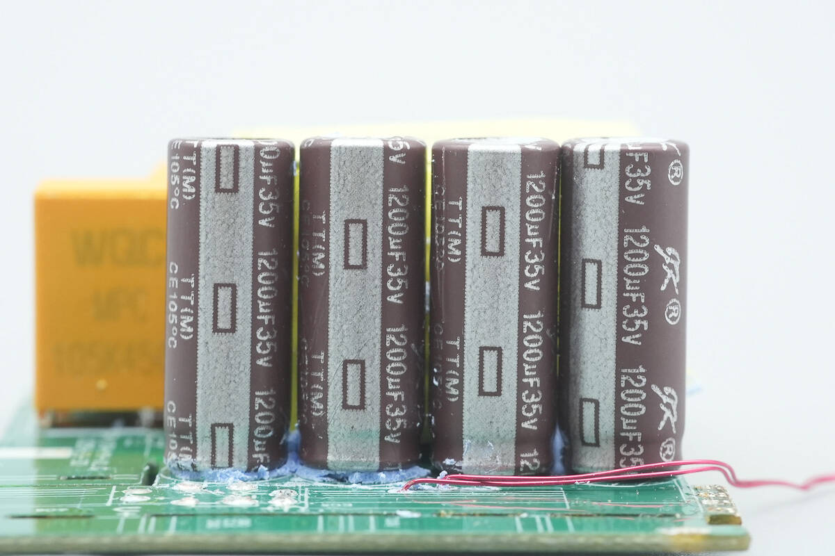
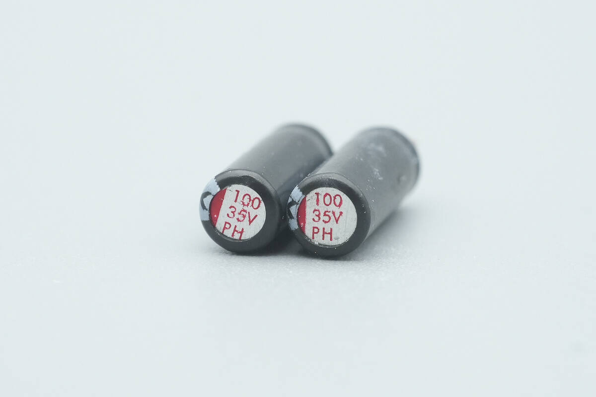
The four capacitors are also from JK, each rated at 35 V, 1200 μF.
The filter inductor is insulated with a heat-shrink tube.
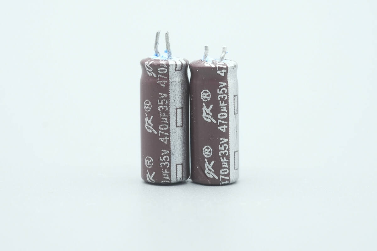
These two capacitors are from JK, each rated at 470 μF, 35 V.
Close-up of the thermistor.
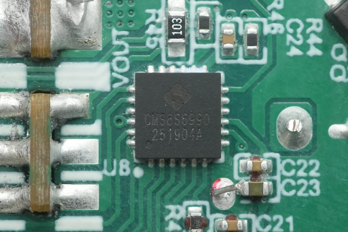
The MCU used for charging control is from Cmsemicon, model CMS8S6990. It is an enhanced 1T8051 Flash MCU, packaged in a QFN24.
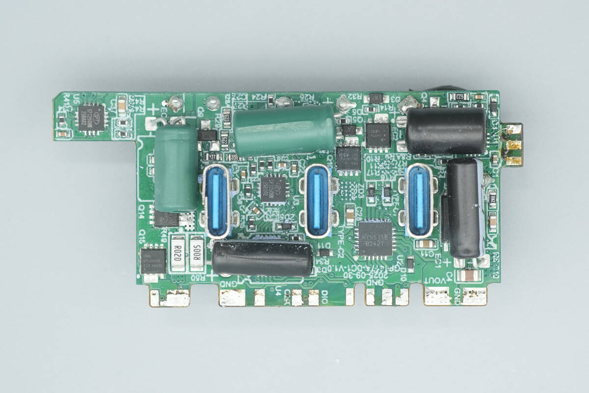
The front side of the output PCB features three synchronous buck circuits with their controllers, synchronous buck MOSFETs, and solid capacitors. Additionally, it houses protocol chips and VBUS MOSFETs.
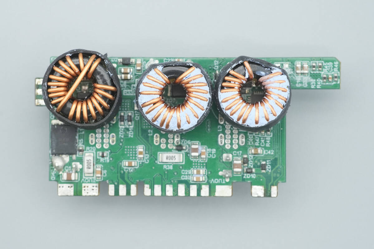
The back side features the buck inductors.
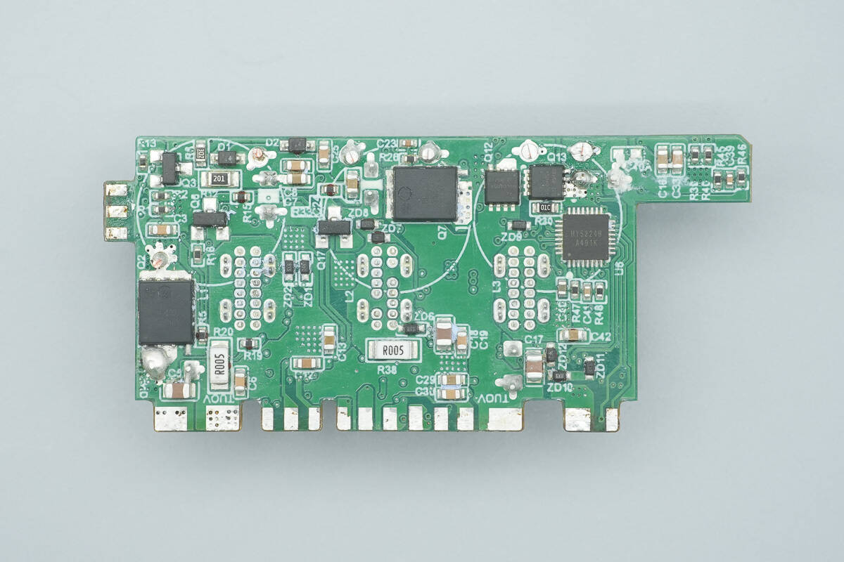
After removing the inductors, the PCB still has synchronous buck MOSFETs and a protocol chip.

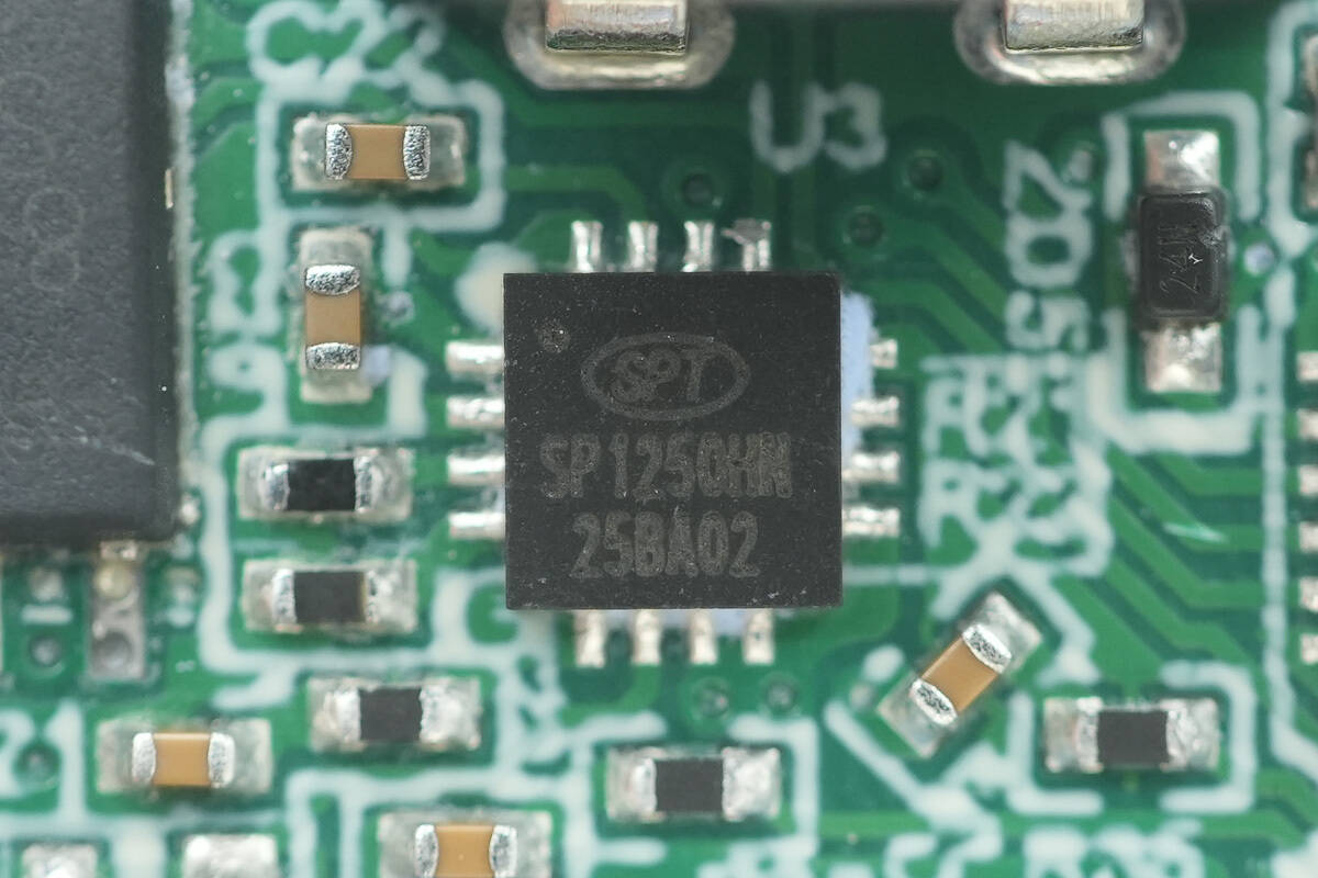
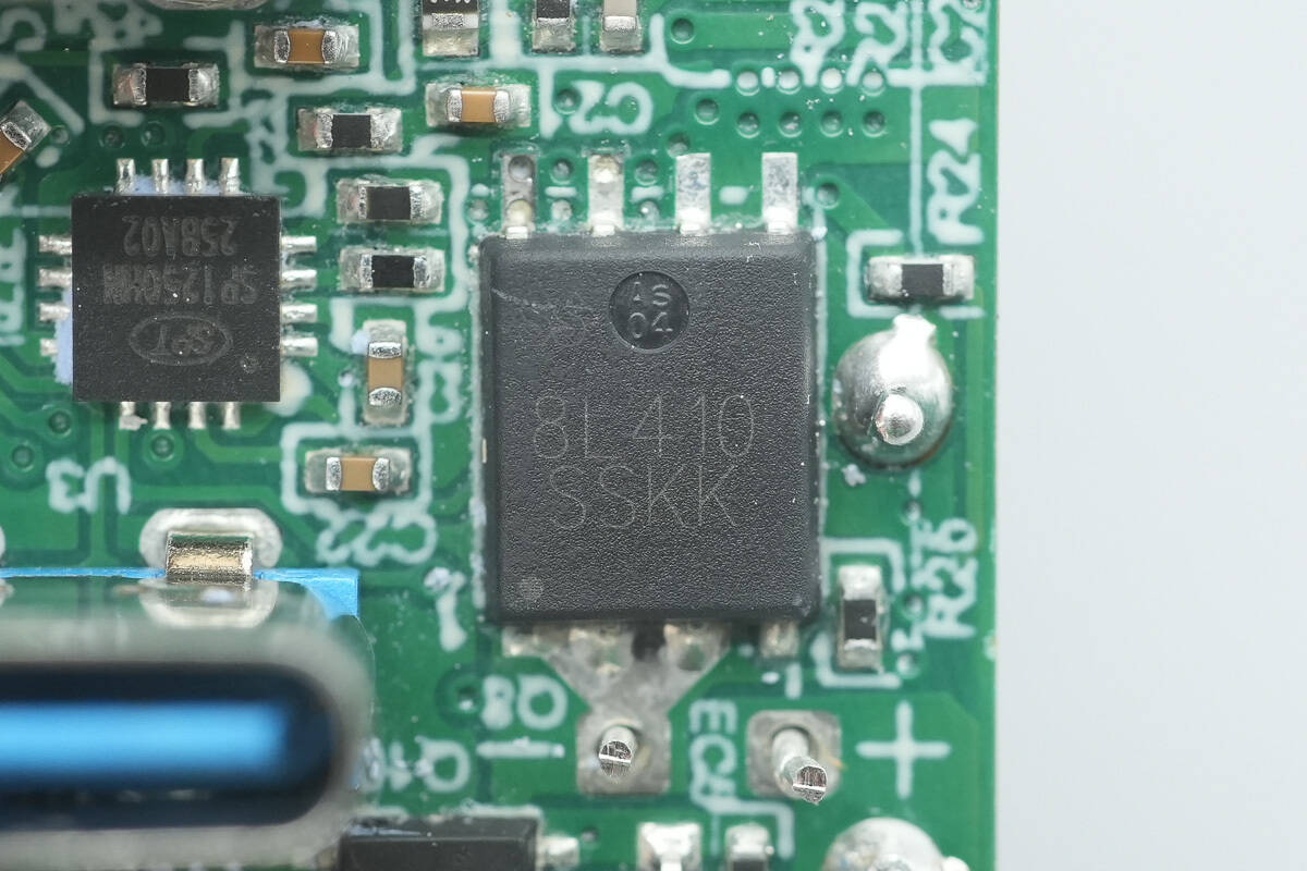
The synchronous buck controller for the USB-C1 port is from Si-Power, model SP1250HN. It supports a wide input voltage range of 9–40 V and a maximum output current of 8 A. The SP1250HN operates in constant-voltage and constant-current modes, with overcurrent protection configurable via external resistors. It integrates adjustable line-loss compensation and supports over-temperature protection, output overcurrent, and short-circuit protection. The chip comes in a QFN 3×3-16L package and is suitable for car chargers and DC-DC converter applications.

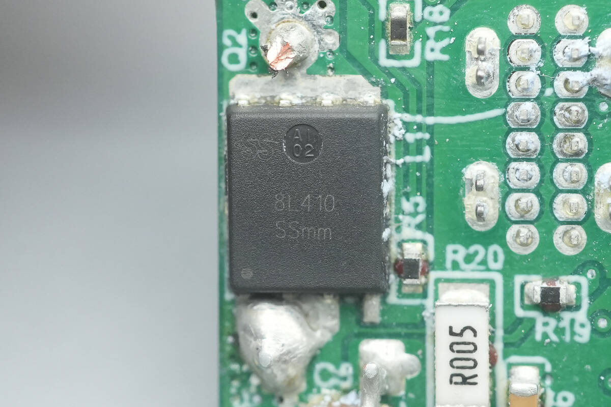
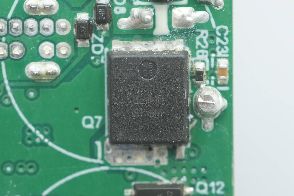
The synchronous buck MOSFET is from AF, model SSC8L410GN6. It is an NMOS transistor with a voltage rating of 40 V and an on-resistance of 4.5 mΩ, packaged in PDFN 5×6-8L.
The other synchronous buck MOSFET is from AF, model SSC8L410TN6. It is an NMOS transistor with a voltage rating of 40 V and an on-resistance of 5.9 mΩ, packaged in PDFN 5×6-8L.
The synchronous buck controller for the USB-C2 port is also the Si-Power SP1250HN.
One of the synchronous buck MOSFETs paired with it is also the AF SSC8L410GN6.
The other synchronous buck MOSFET is from AF, model SSC8L410TN6.
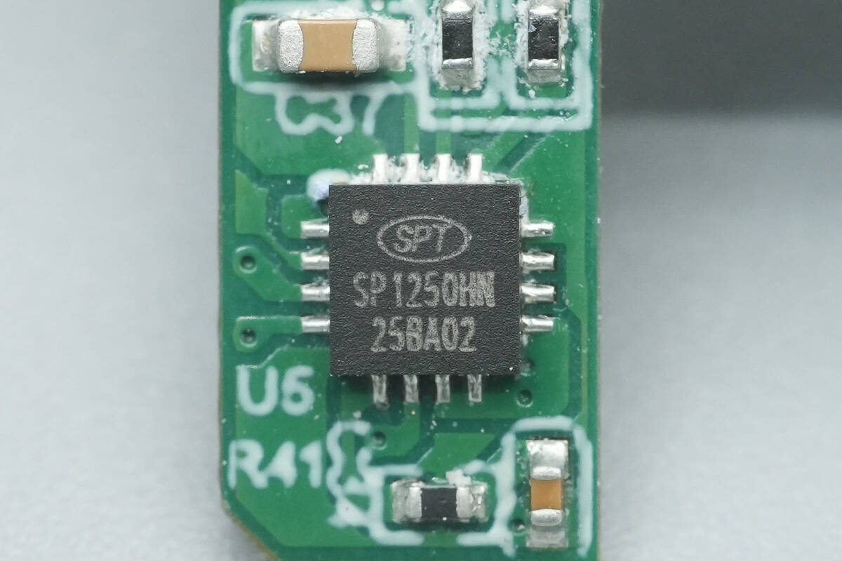
The synchronous buck controller for the USB-C3 and USB-A ports is from Si-Power, model SP1250HN.
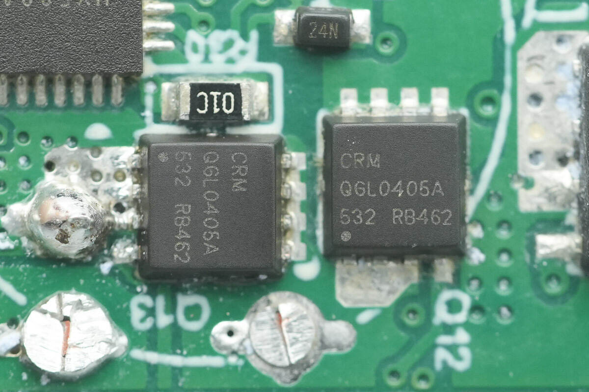
The two synchronous buck MOSFETs paired with it are from CRM, model CRMQGL0405A. They are NMOS transistors with a voltage rating of 40 V, packaged in PDFN 3.3×3.3-8L.

Close-up of the three secondary buck inductors.

The secondary filter solid capacitors are all insulated with plastic sleeves. This one is from JSH, rated at 35 V, 150 μF.
The other two capacitors are rated at 35 V, 100 μF.
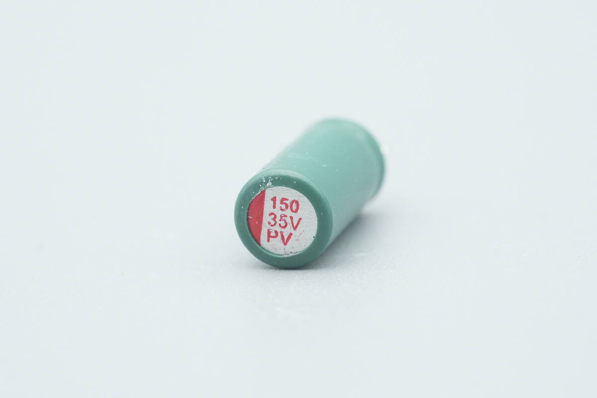
There is also one capacitor rated at 35 V, 150 μF.
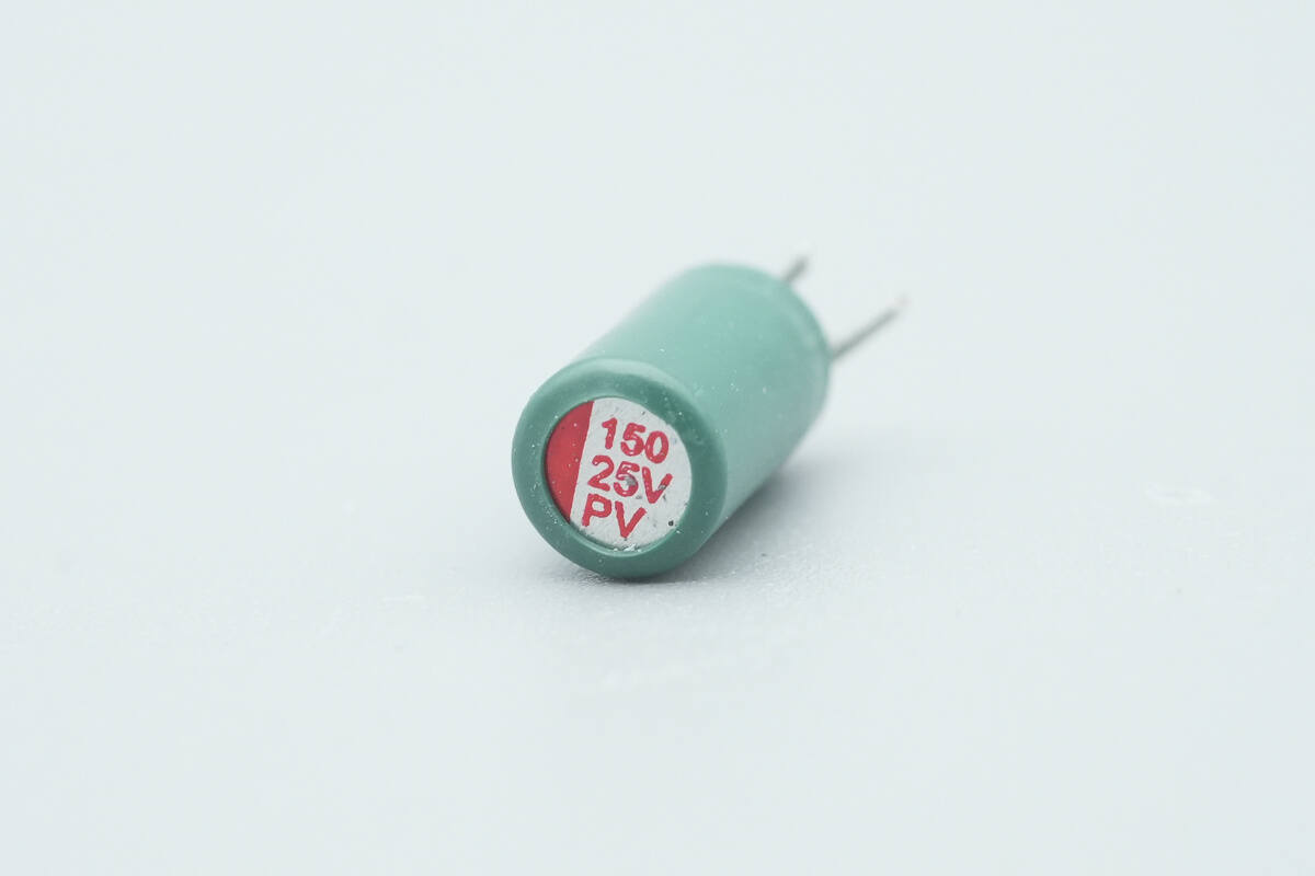
The last capacitor is rated at 25 V, 150 μF.

The protocol chip for the USB-C1 port is from HYASiC, model HY5515E. It is a USB Type-C port controller with a built-in 32-bit MCU, integrating 32 kB MTP, 128-bit e-Fuse ROM, and 4 kB SRAM. The chip complies with the latest USB Type-C and PD standards and provides cable insertion and orientation detection for a single USB-C port. Once a cable is detected, the HY5515E communicates via the CC pins using the USB PD protocol.
Leveraging HYASiC’s proprietary technology, the HY5515E offers extensive functionality and design flexibility. It integrates all the termination resistors required for a Type-C port, feedback control circuits for VBUS voltage regulation, and constant-current adjustment circuits. Its highly integrated design requires minimal external components and, with multiple built-in functions and protection mechanisms, significantly enhances system reliability. The chip comes in a QFN24 package.

The protocol chip for the USB-C2 port is also from HYASiC, model HY5515E.

The VBUS MOSFETs for the USB-C1 and USB-C2 ports are from CRM, model CRMQBL0407A. They are PMOS transistors with a voltage rating of –40 V and an on-resistance of 7.7 mΩ, packaged in PDFN 3.3×3.3-8L.
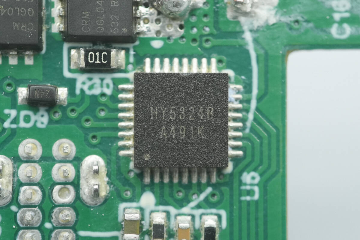
The protocol chip for the other two ports is from HYASiC, model HY5324. This is a high-performance, highly integrated multi-port USB fast-charging controller. It supports seven programmable PDOs and is compatible with BC1.2 DCP, Apple 2.4 A, QC2.0/QC3.0/QC3.0+, AFC, FCP, SCP, UFCS, and PE+ 1.1/2.0 protocols.
The HY5324 integrates multiple protection features, including overvoltage protection (OVP), undervoltage lockout (UVLO), overcurrent protection (OCP), output short-circuit protection, CC or DPDM overvoltage protection, and over-temperature protection. It comes in a QFN-32L package (4 mm × 4 mm).
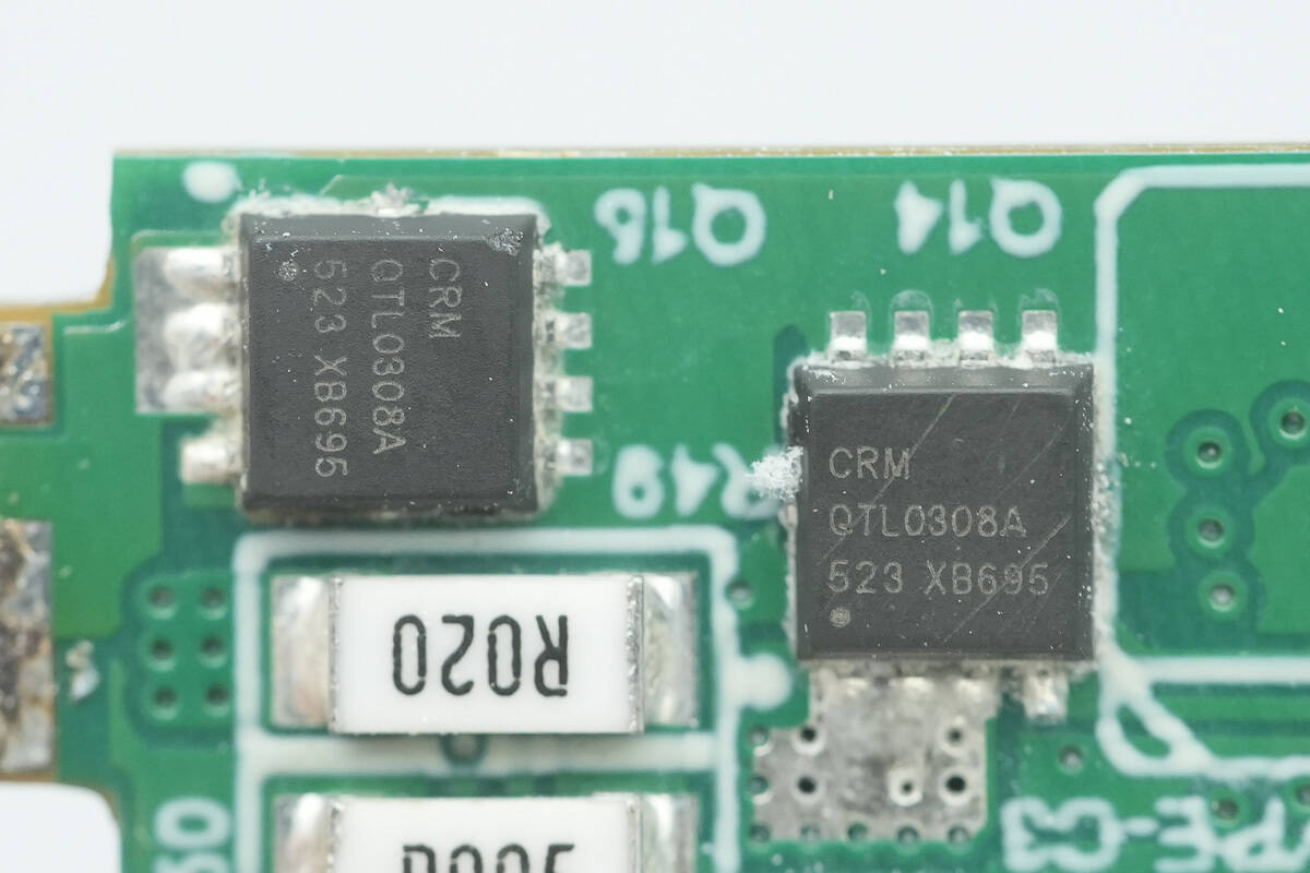
The VBUS MOSFETs for the USB-C3 and USB-A ports are from CRM, model CRMQTL0308A. They are NMOS transistors with a voltage rating of 30 V and an on-resistance of 6.2 mΩ, packaged in PDFN 3.3×3.3-8L.
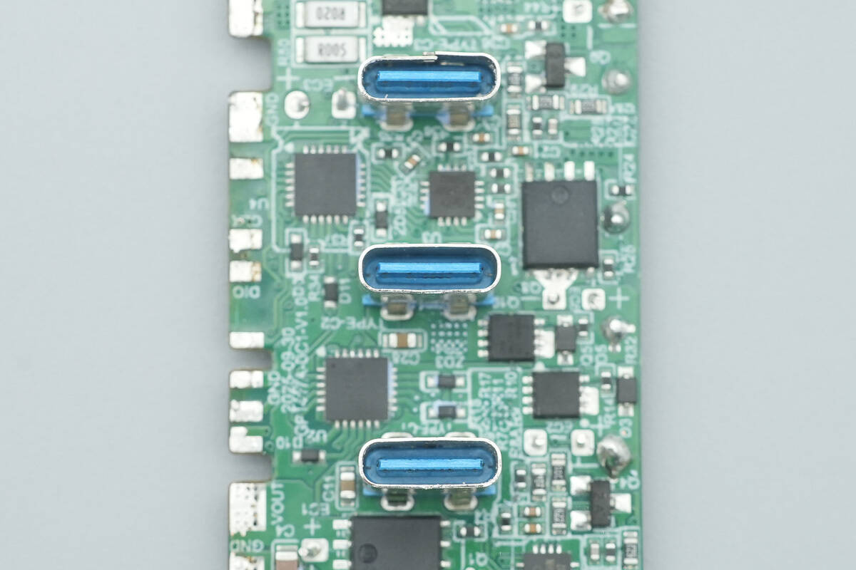
Close up of the USB-C sockets.
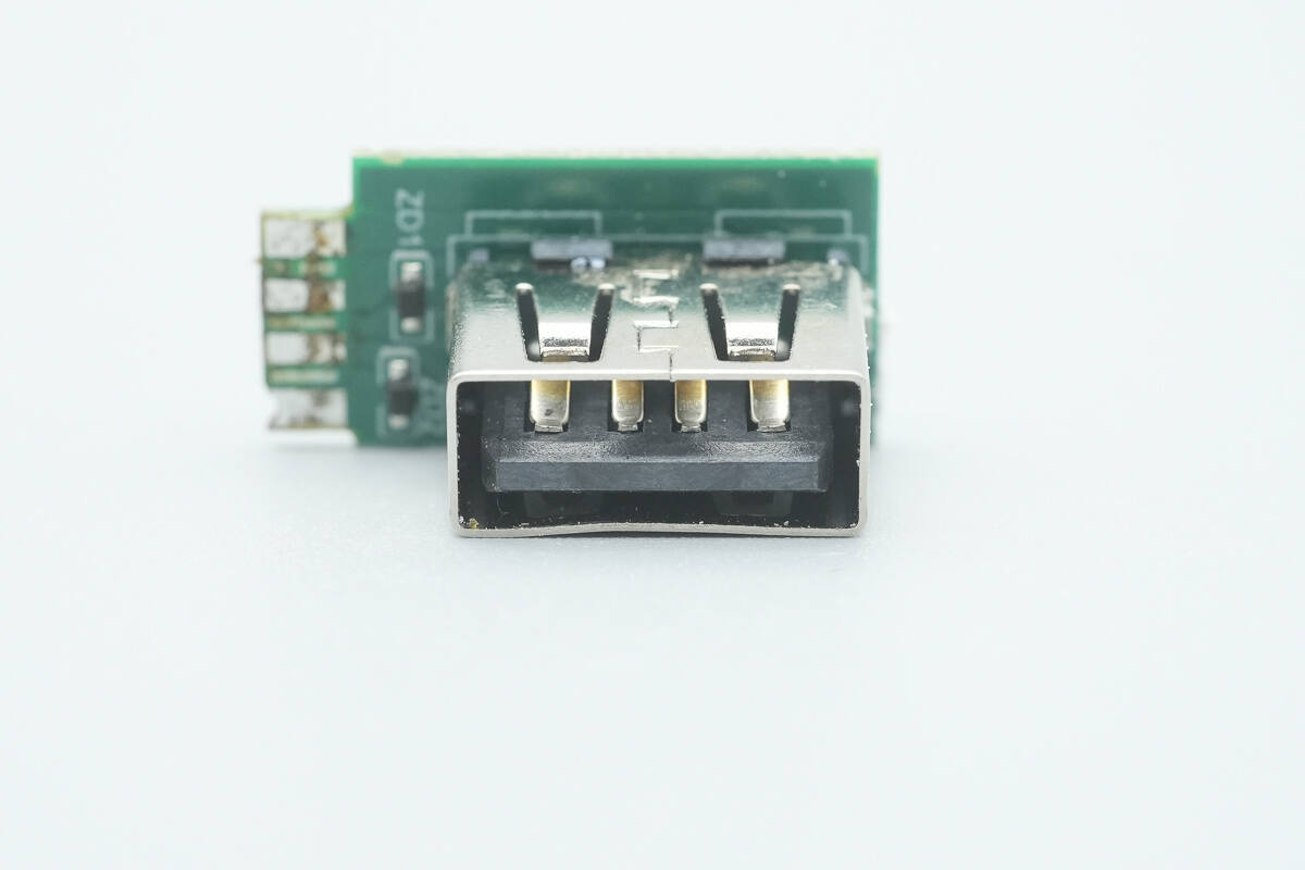
The USB-A socket is soldered onto a separate PCB.
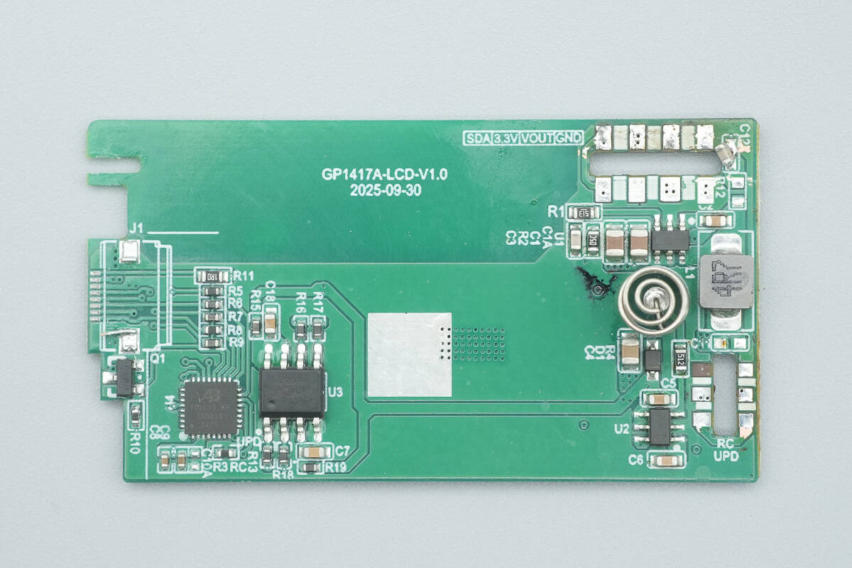
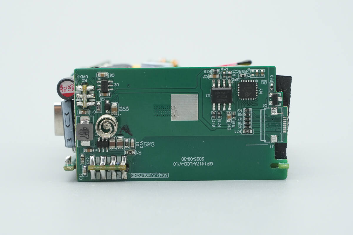
The front side of another small PCB houses an MCU, memory, a synchronous buck converter, a buck inductor, and a touch-sensing chip, among other components.
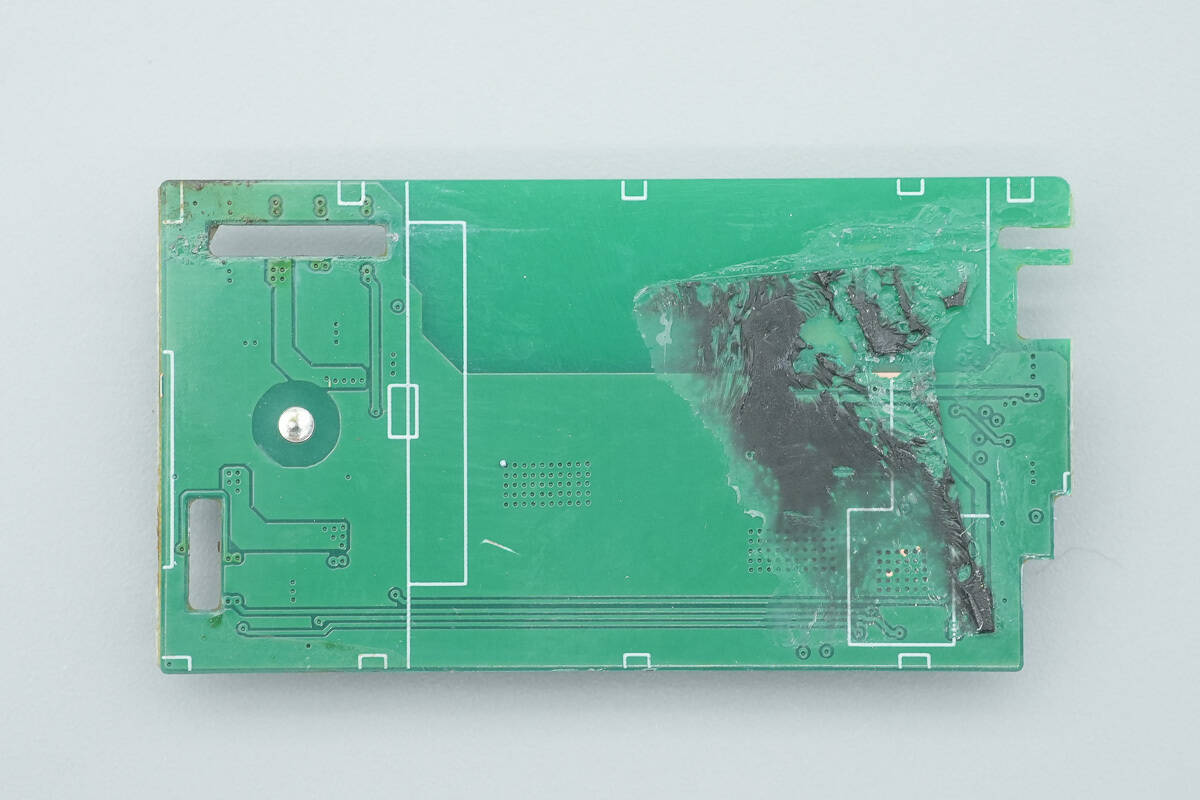
The back side has no components.
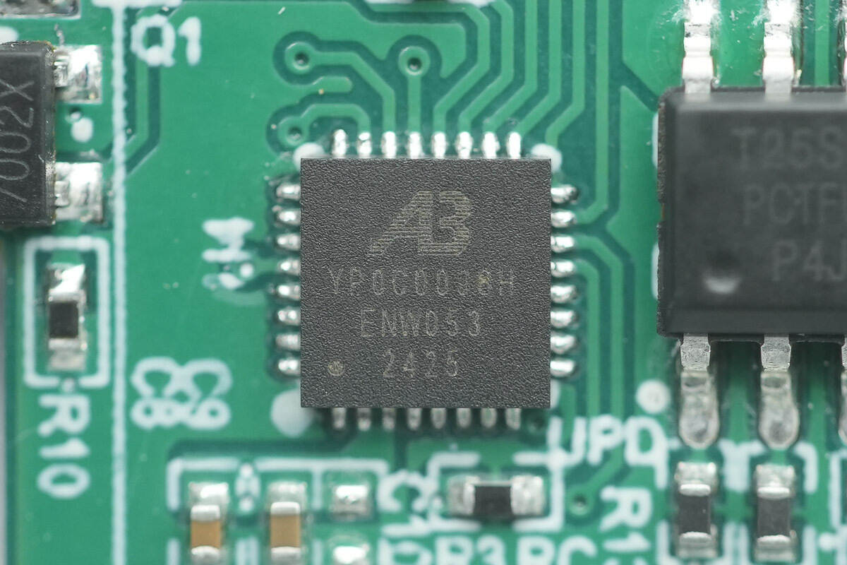
The MCU is marked YP0C0038H and comes in a QFN32 package.
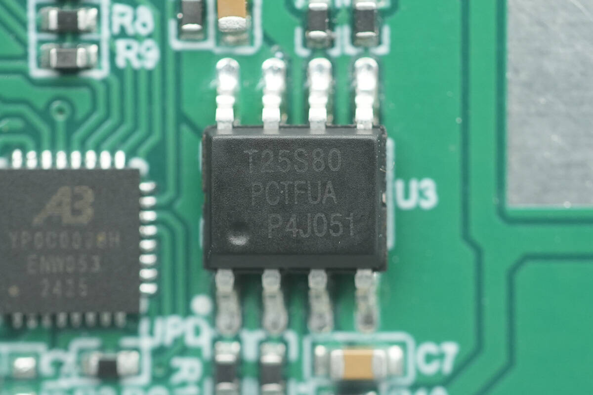
The memory is marked T25S80, with a capacity of 1 MB, and comes in an SOIC8 package.
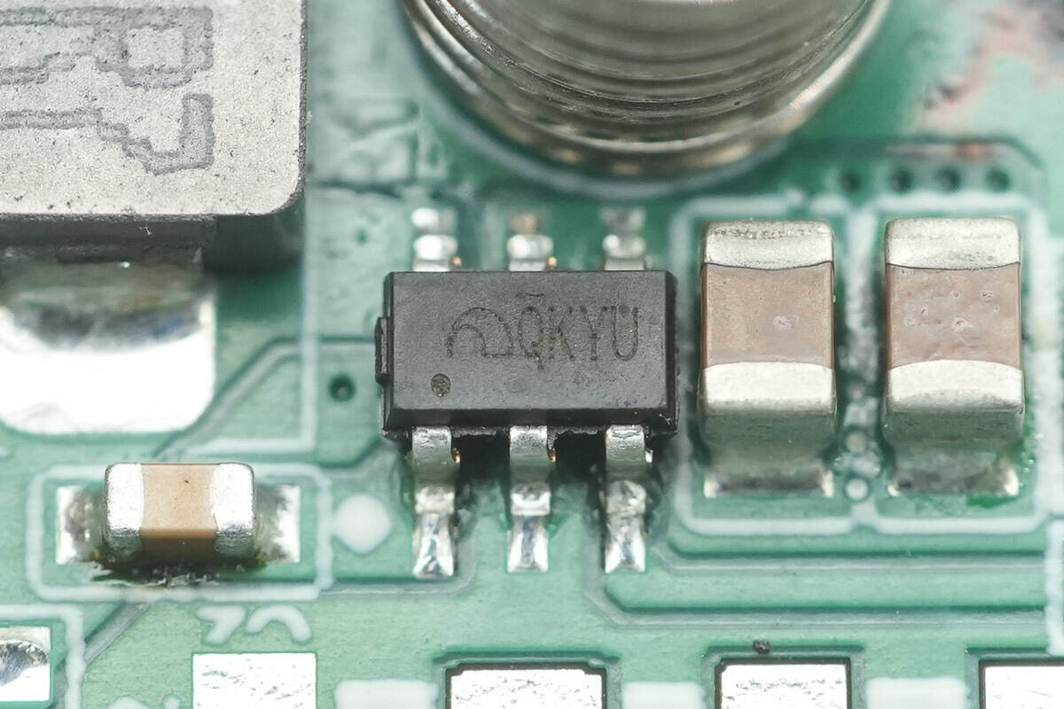
The synchronous buck converter used for step-down power supply is marked QKYU.
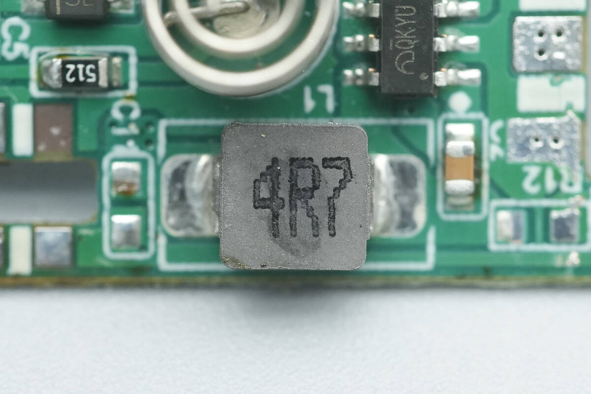
Close-up of the 4.7 μH buck inductor.
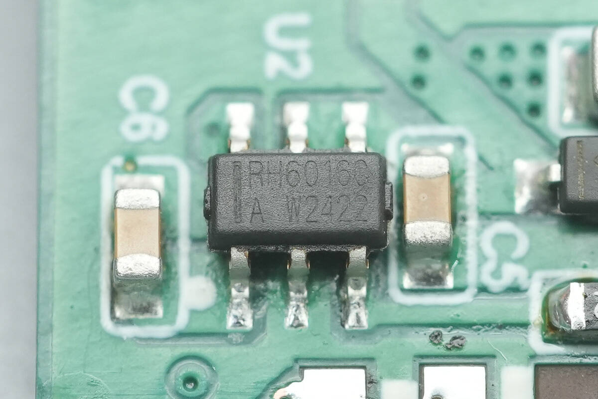
The touch-sensing chip is model RH6016C. It features a single-channel capacitive input with a built-in voltage regulator, high-precision voltage stabilization, power-on reset and low-voltage reset, as well as hardware debounce and other anti-interference measures.
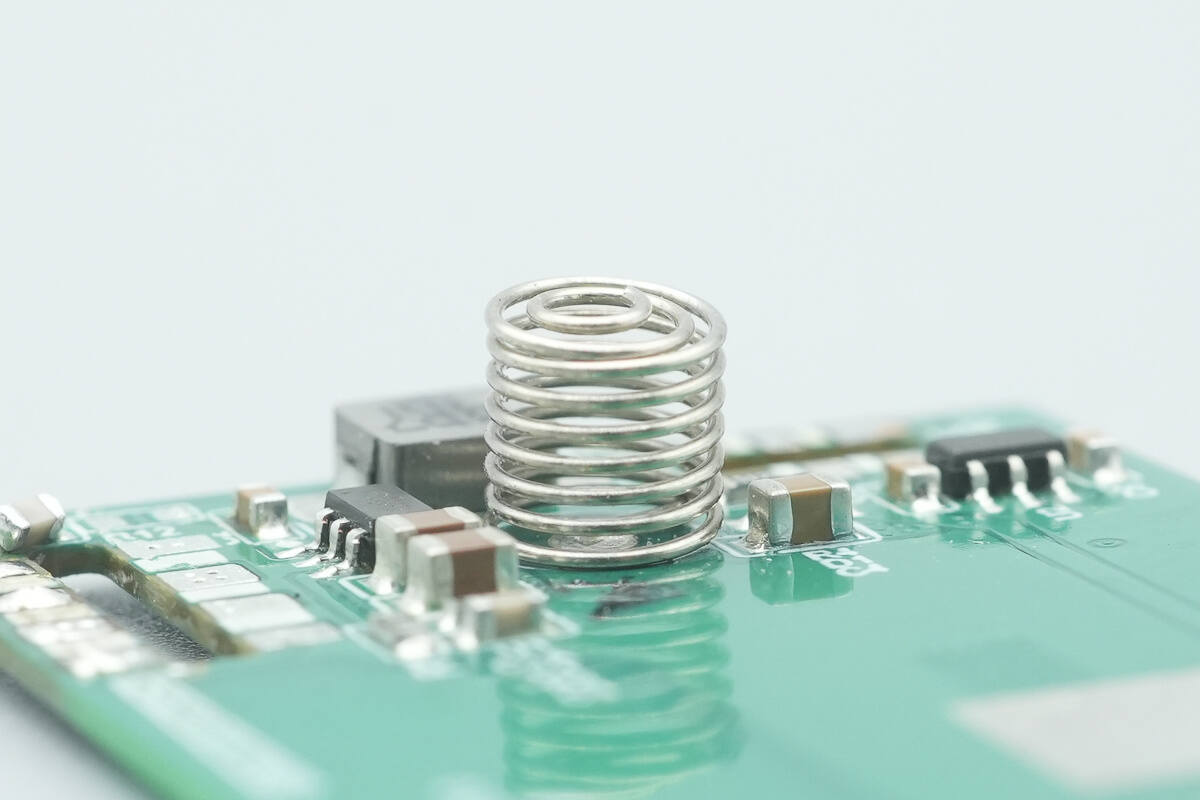
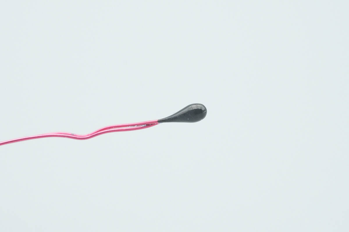
Close-up of the touch spring.

Well, those are all components of the MIIIW 140W GaN Charger CA514 Pro.
Summary of ChargerLAB
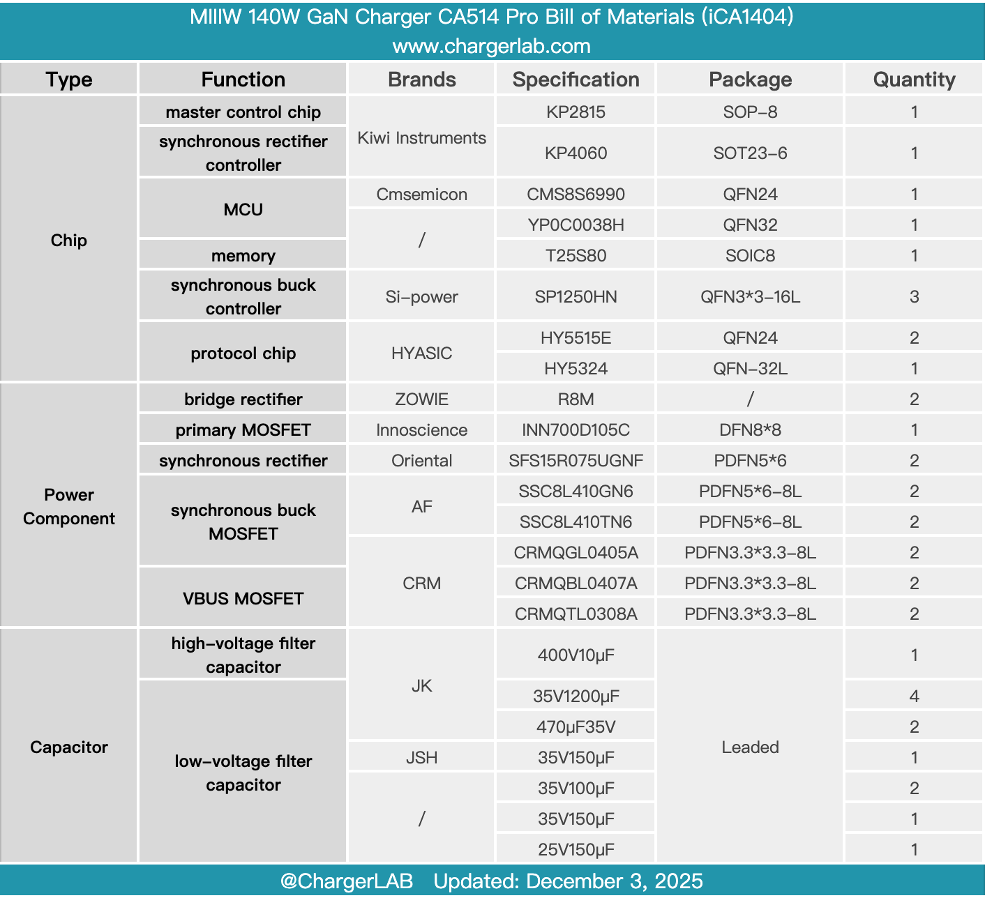
Here is the component list of the MIIIW 140W GaN Charger CA514 Pro for your convenience.
It features a borderless TFT display that shows per-port power, total power, temperature, and other information. The charger is equipped with three USB-C ports and one USB-A port, supporting UFCS, PD 3.1/PPS, SCP, and other protocols, as well as Xiaomi’s proprietary fast-charging protocol.
After taking it apart, we found that it uses a single-stage high-PF power design with Kiwi Instruments KP2815 and KP4060, paired with Innoscience INN700D105C GaN power device. It features three independent secondary DC-DC buck circuits, all using the Si-Power SP1250HN buck solution. Output control is handled by HYASiC HY5515E and HY5324 protocol chips.
The PCBA module is filled with potting compound and covered with heatsinks to aid heat dissipation. A thermistor is used for temperature monitoring, and paired with the TFT display, they provide visible safety feedback.
Related Articles:
1. Teardown of IM Motors 50W In-Car Pre-installed Wireless Charging Module
2. Teardown of BYD 50W In-Car Pre-installed Wireless Charging Module
3. Teardown of CUKTECH 10 100W Car Charger with Retractable Cable (CC903P)