Introduction
Lenovo’s sub-brand thinkplus has launched a high-power power bank featuring a visual design paired with a high-definition digital display, delivering an impressive look and user experience. It supports fast charging at up to 140W and is compatible with Moto smartphones for up to 125W fast charging. With support for fast-charging protocols such as PPS and SCP, it is also well-suited for devices from brands like Samsung and Huawei. Equipped with an industry-first digital hybrid charging technology, it supports simultaneous charging and discharging, helping to reduce desktop clutter.
It is equipped with EVE automotive-grade battery cells, with an energy capacity of 73Wh, and has passed CCC certification, making it safe to carry on airplanes. The large 20,000mAh capacity ensures ample power supply. Now, let's take a closer look at the craftsmanship and materials.
Product Appearance
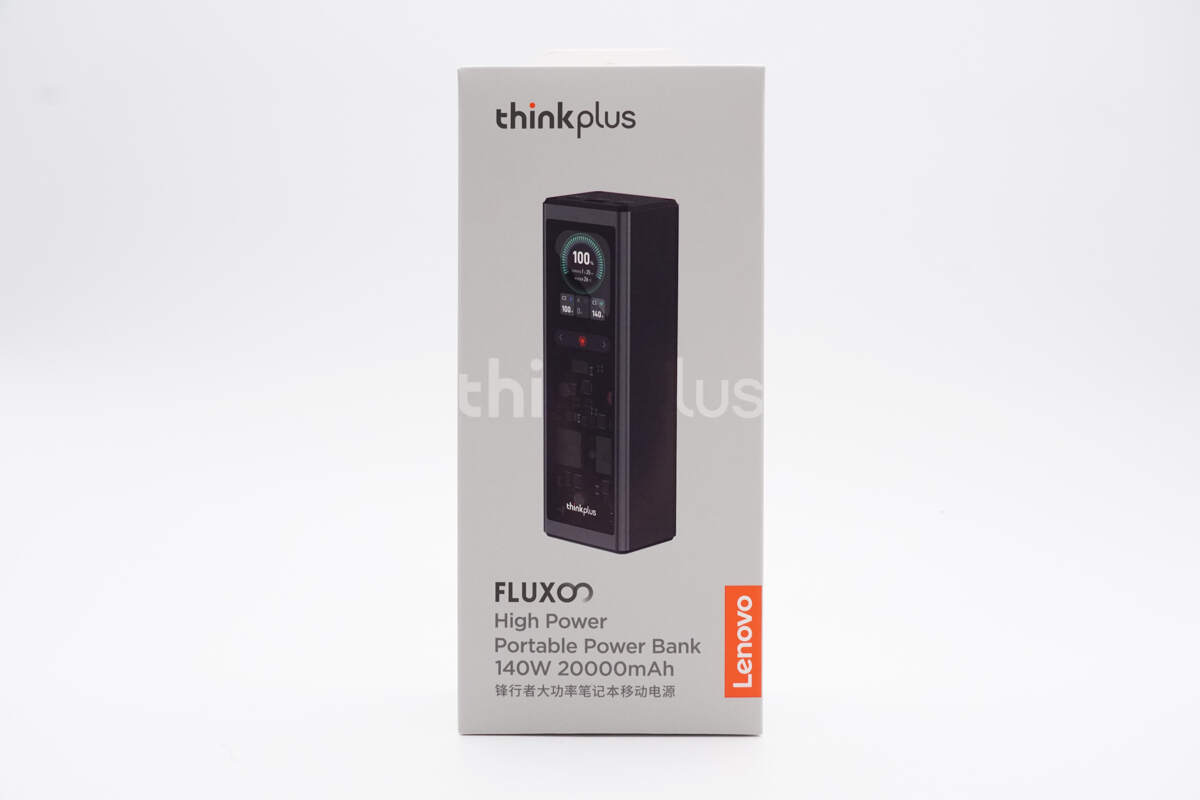
The front of the packaging box features the Lenovo and thinkplus logos, along with an image of the power bank’s exterior.
As a high-power portable charger, it is compatible with a wide range of devices, including laptops, smartphones, tablets, headphones, smartwatches, and digital cameras.
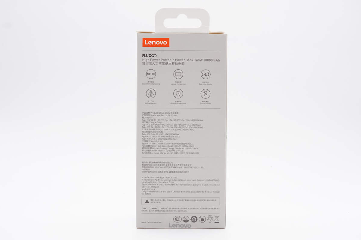
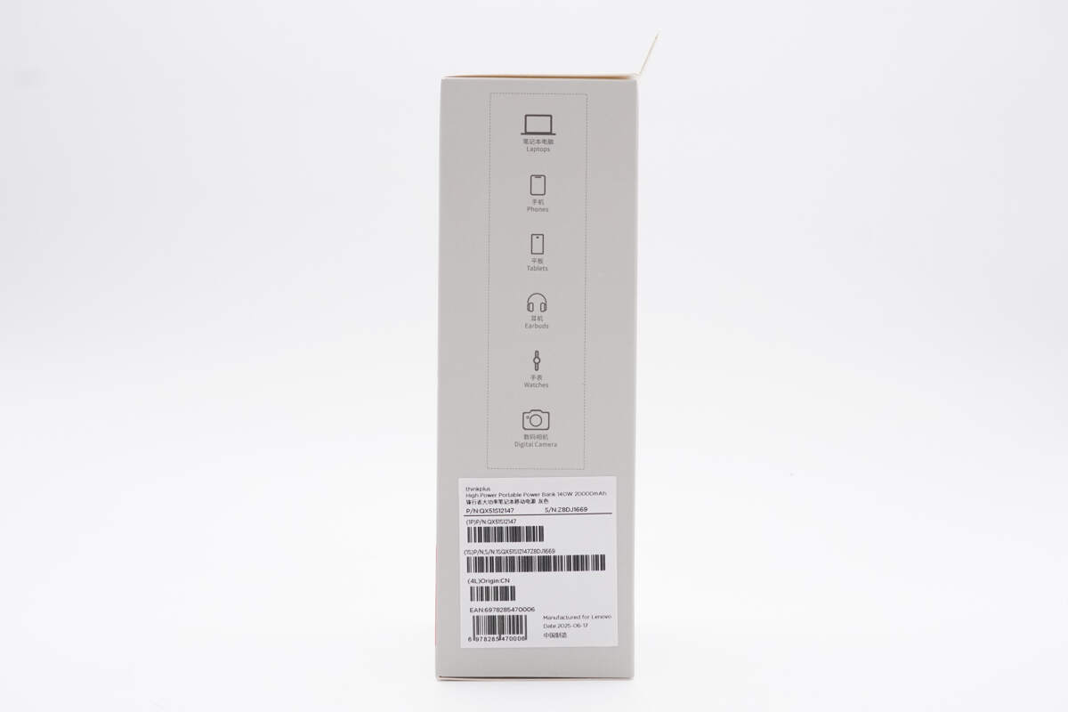
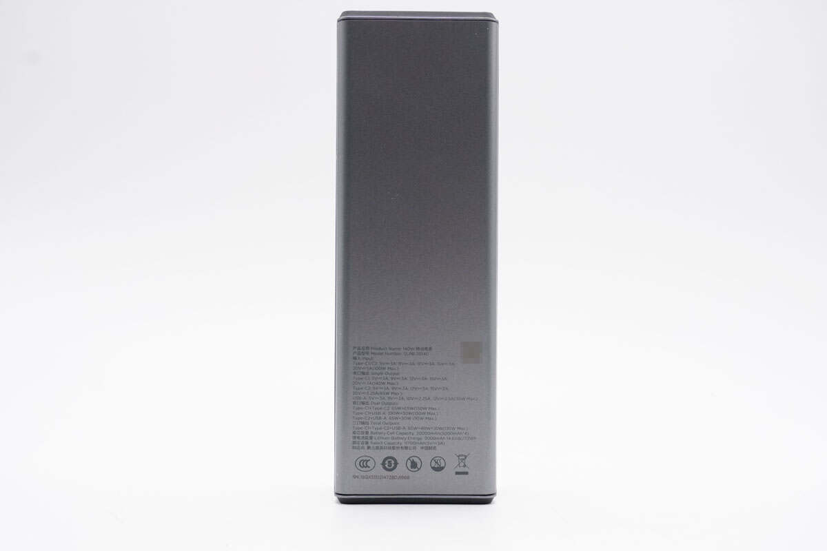
The back of the packaging displays the selling points, spec info, and important notices.
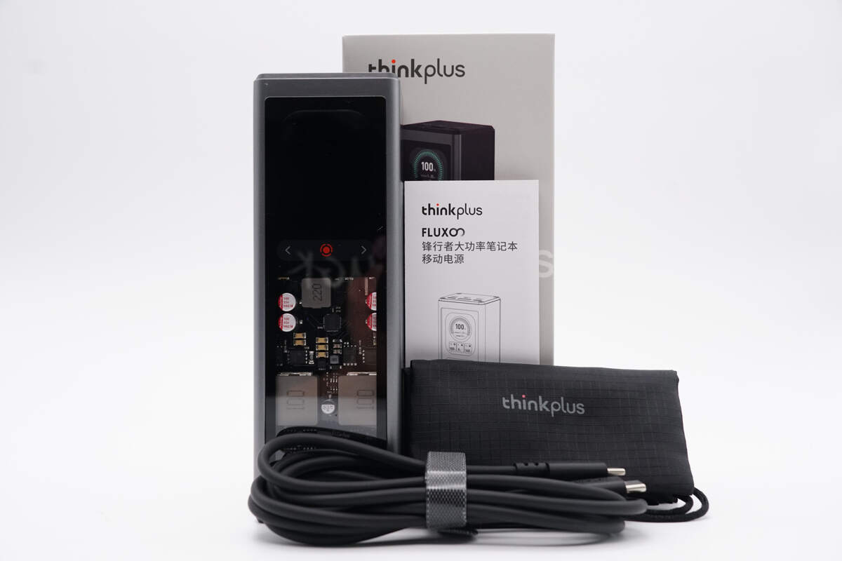
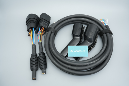
The package includes the power bank, cable, and more.
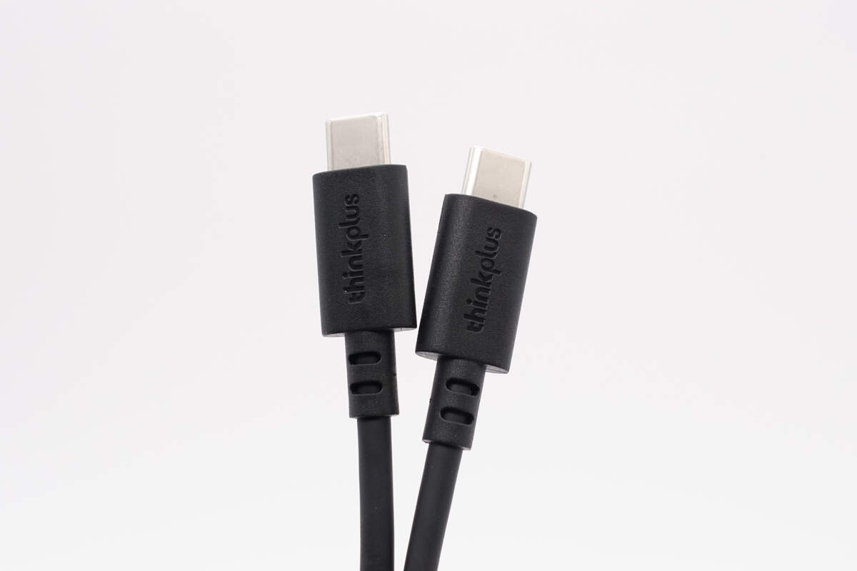
The included cable is a dual USB-C type.
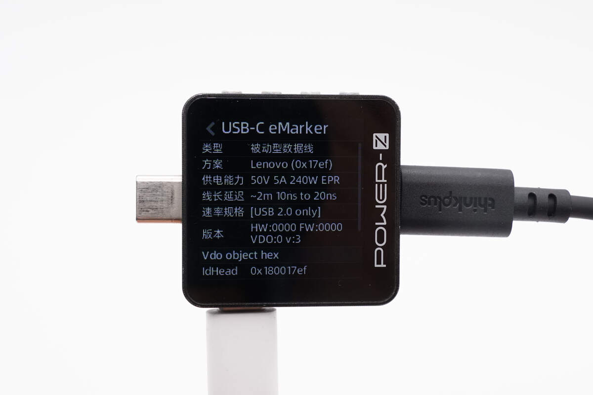
The ChargerLAB POWER-Z KM003C indicates that the cable has an E-Marker chip and supports Power Delivery of 50V/5A, enabling PD3.1 fast charging up to 240W. It also supports 20V/7A at 140W, allowing it to handle a high current of 7A.
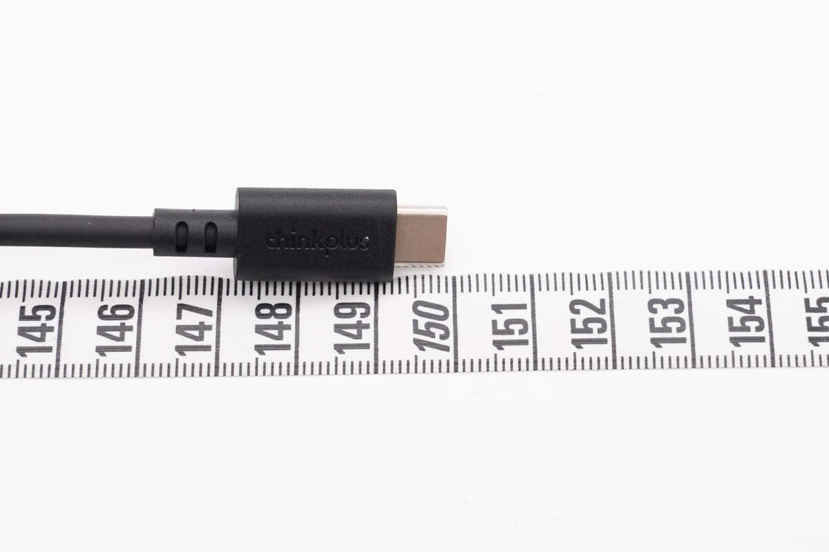
The length of the cable is about 1.5 m (4.92 feet).
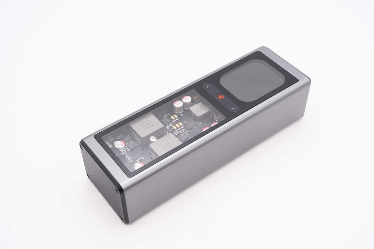
It features a silver-gray casing with a transparent window design, paired with a TFT interactive color screen. Whether in terms of visuals or user experience, it delivers a strong sense of cutting-edge technology.
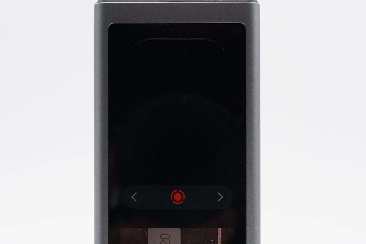
The built-in 2.01-inch display provides real-time information, including remaining battery percentage, estimated available usage time, battery temperature, and the charging/discharging power of each port. The function keys at the bottom feature a touch-sensitive design.
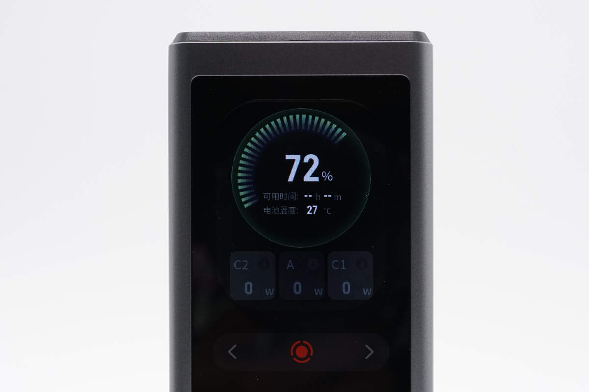
The TFT screen can display real-time information such as remaining battery percentage, estimated available usage time, battery cell temperature, and the output power of each port. It also features a sporty car dashboard design, adding a strong sense of ceremony.
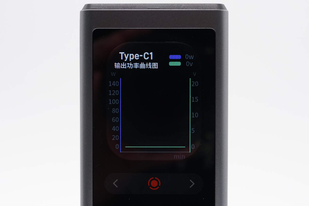
Additionally, through the touch-sensitive function keys, users can bring up the output power curve for each USB port, allowing the device to display both real-time power and charging power variations over time.
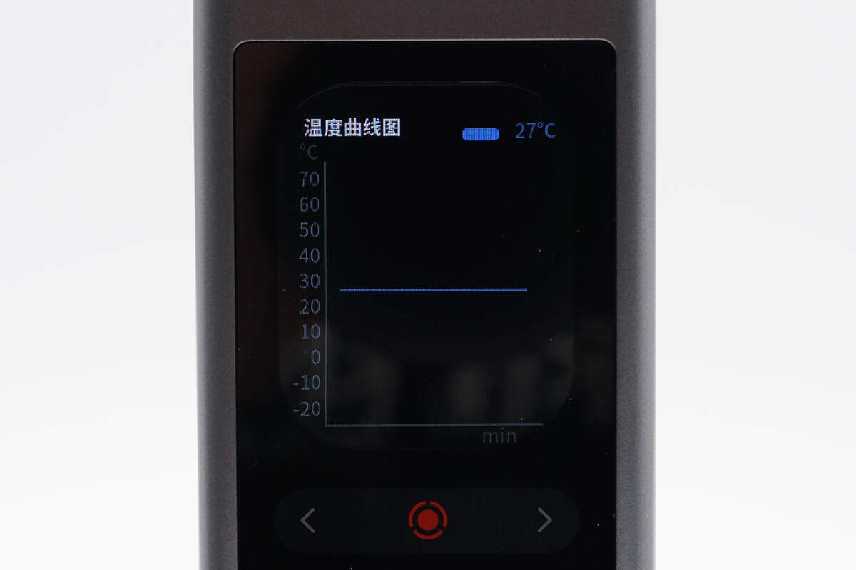
The screen can also show changes in battery cell temperature in a very clear and intuitive way, which is a highly useful feature.
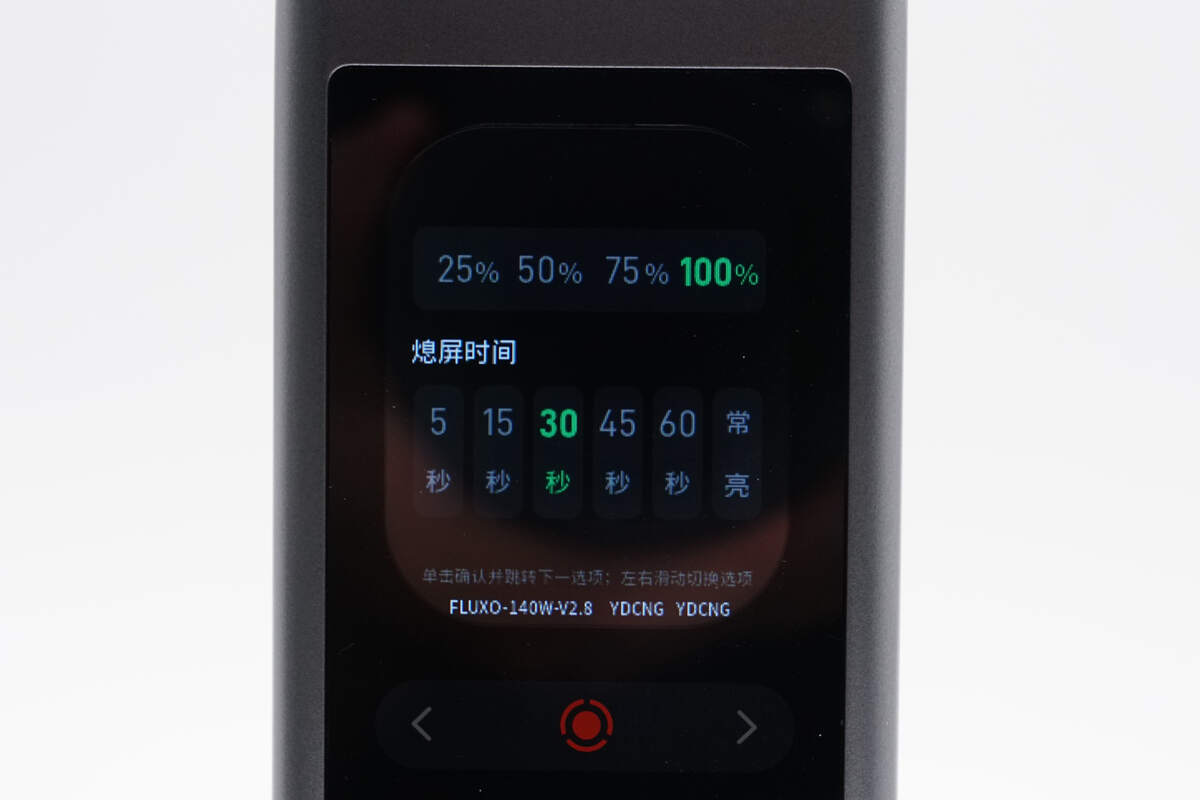
It supports brightness and screen-off time settings, offering greater flexibility to meet different user preferences.
There is also a specially designed thinkplus brand display interface.
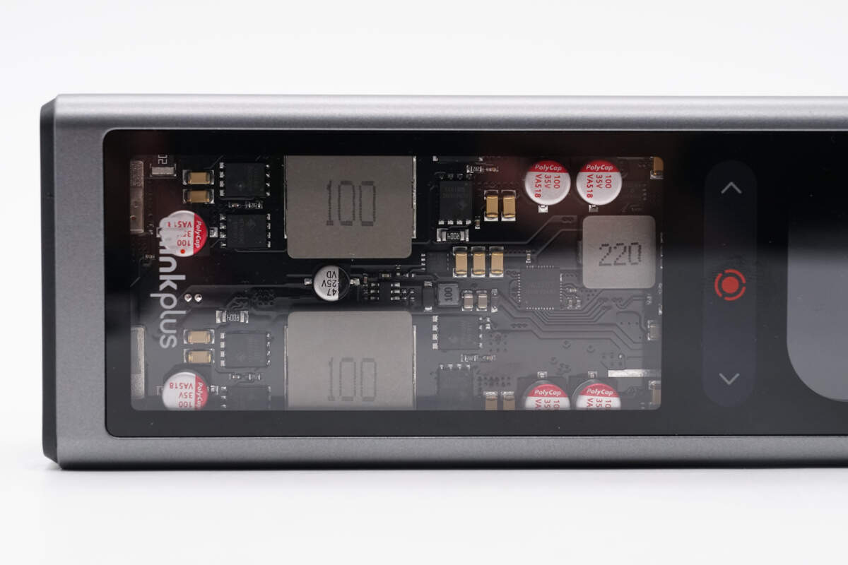
The transparent window at the bottom reveals internal components such as chips, capacitors, and inductors, fully showcasing industrial design aesthetics.
The bottom also features the thinkplus logo.
The back displays the spec information.
Model: SLPB-20140
Input:
Type-C1/C2: 5V3A, 9V3A, 12V3A, 15V3A, 20V5A (100W Max)
Single Output:
Type-C1: 5V3A, 9V3A, 12V3A, 15V3A, 20V7A (140W Max)
Type-C2: 5V3A, 9V3A, 12V3A, 15V3A, 20V3.25A (65W Max)
USB-A: 5V3A, 9V3A, 10V2.25A, 12V2.5A (30W Max)
Dual Outputs:
Type-C1 + Type-C2: 65W + 65W (130W Max)
Type-C1 + USB-A: 100W + 30W (130W Max)
Type-C2 + USB-A: 65W + 30W (95W Max)
Total Outputs:
Type-C1 + Type-C2 + USB-A: 65W + 40W + 30W (135W Max)
Battery Capacity: 20,000mAh (5,000mAh × 4)
Lithium Battery Energy: 5,000mAh 14.6Vdc / 73Wh
Rated Capacity: 11,700mAh (5V3A)
It has passed the CCC certification with the certification number 202501094769340, allowing it to be carried on airplanes and high-speed trains. Additionally, Lenovo offers an 18-month warranty for the product, providing a replacement (not repair) for any non-human-caused quality issues, strongly backing the product’s quality.
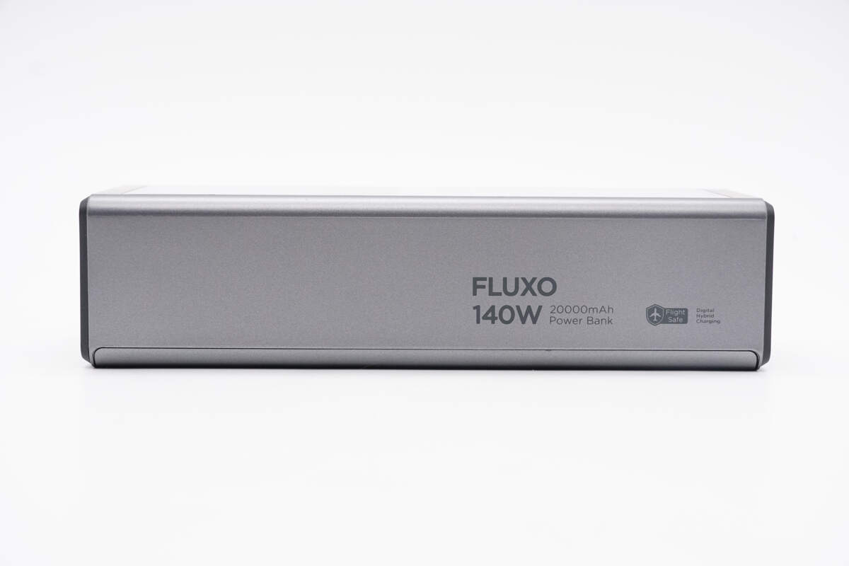
The side is printed with FLUXO 140W and a fight-safe logo.
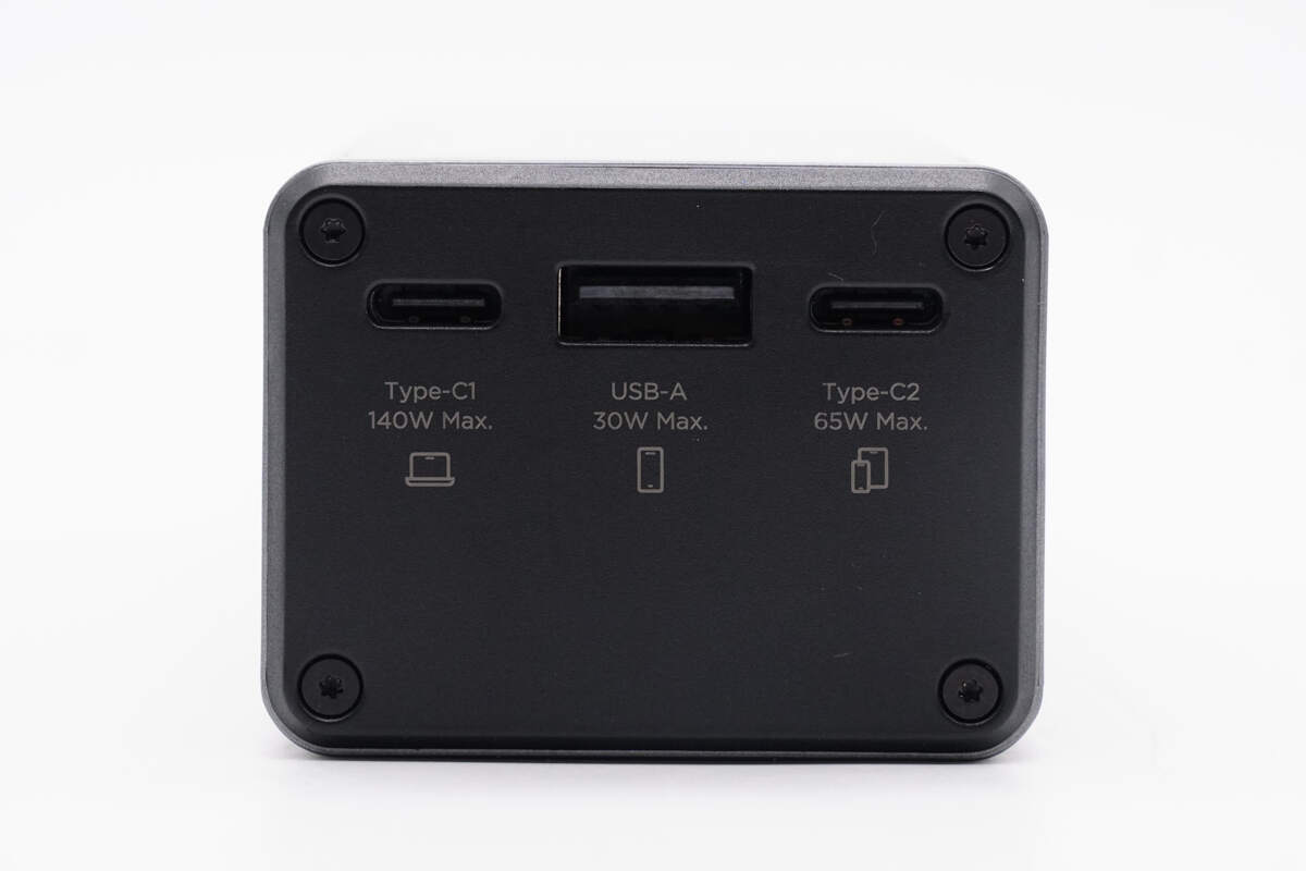
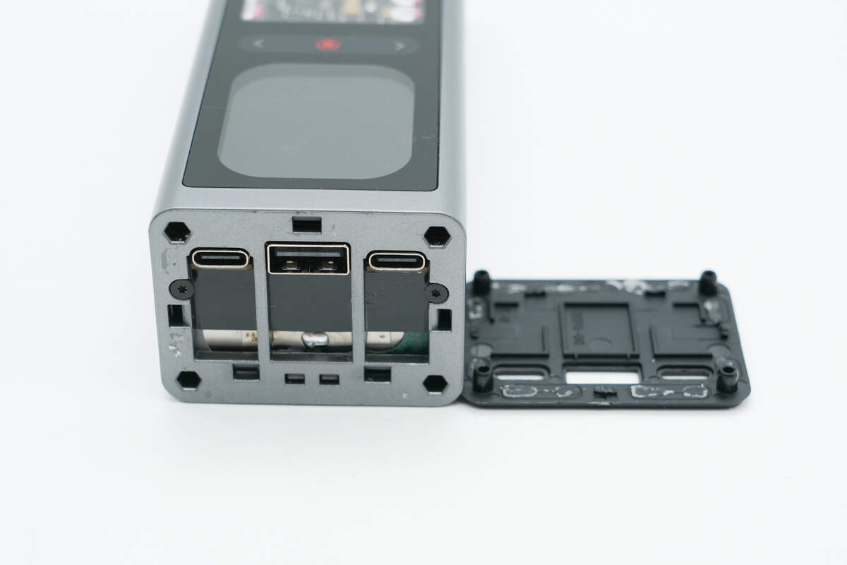
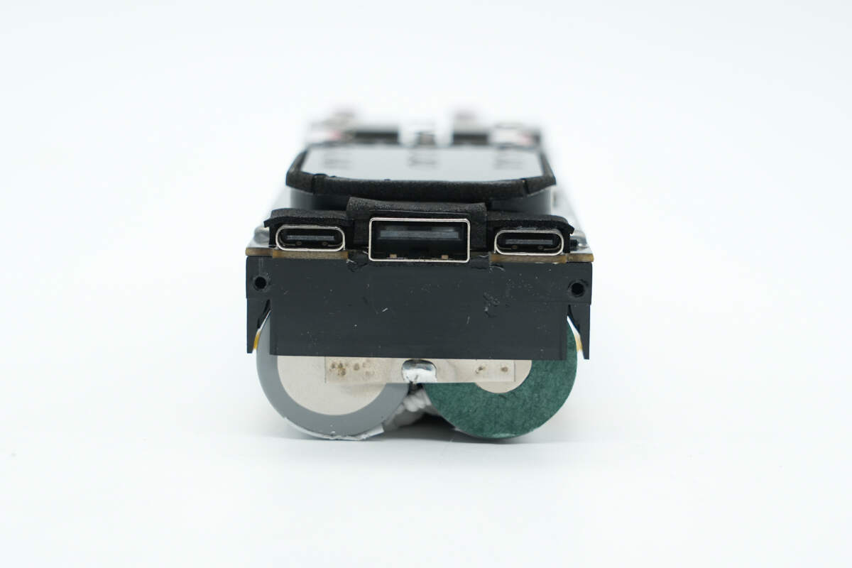
The top is equipped with two USB-C ports and one USB-A port, with screws located at all four corners.
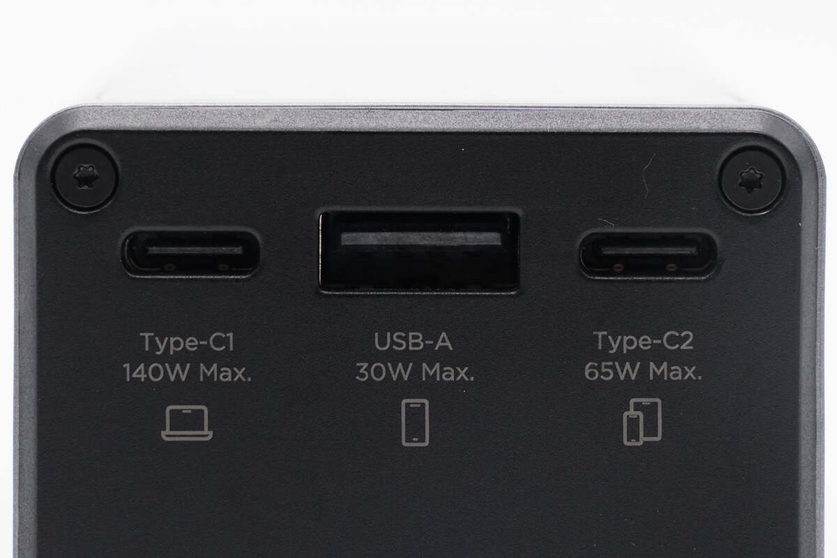
Next to each of the three ports, their respective maximum output power is indicated.
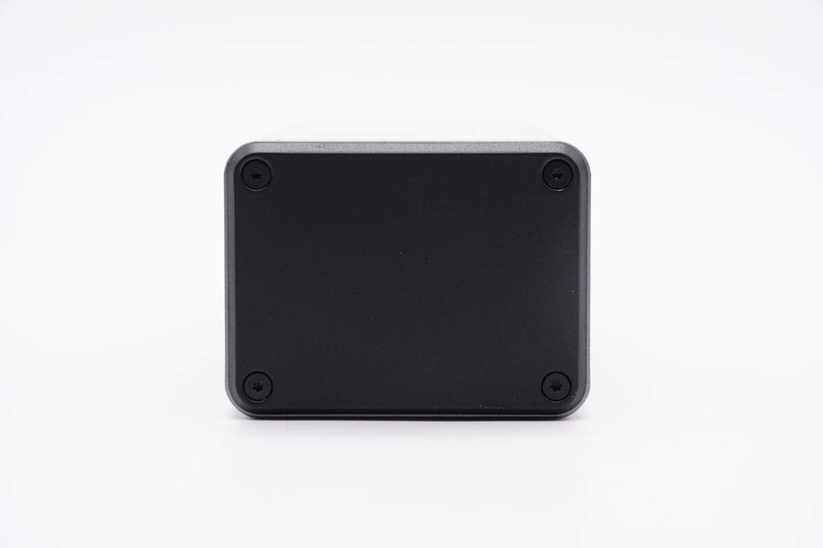
The bottom features a matte finish, with screws also located at all four corners.
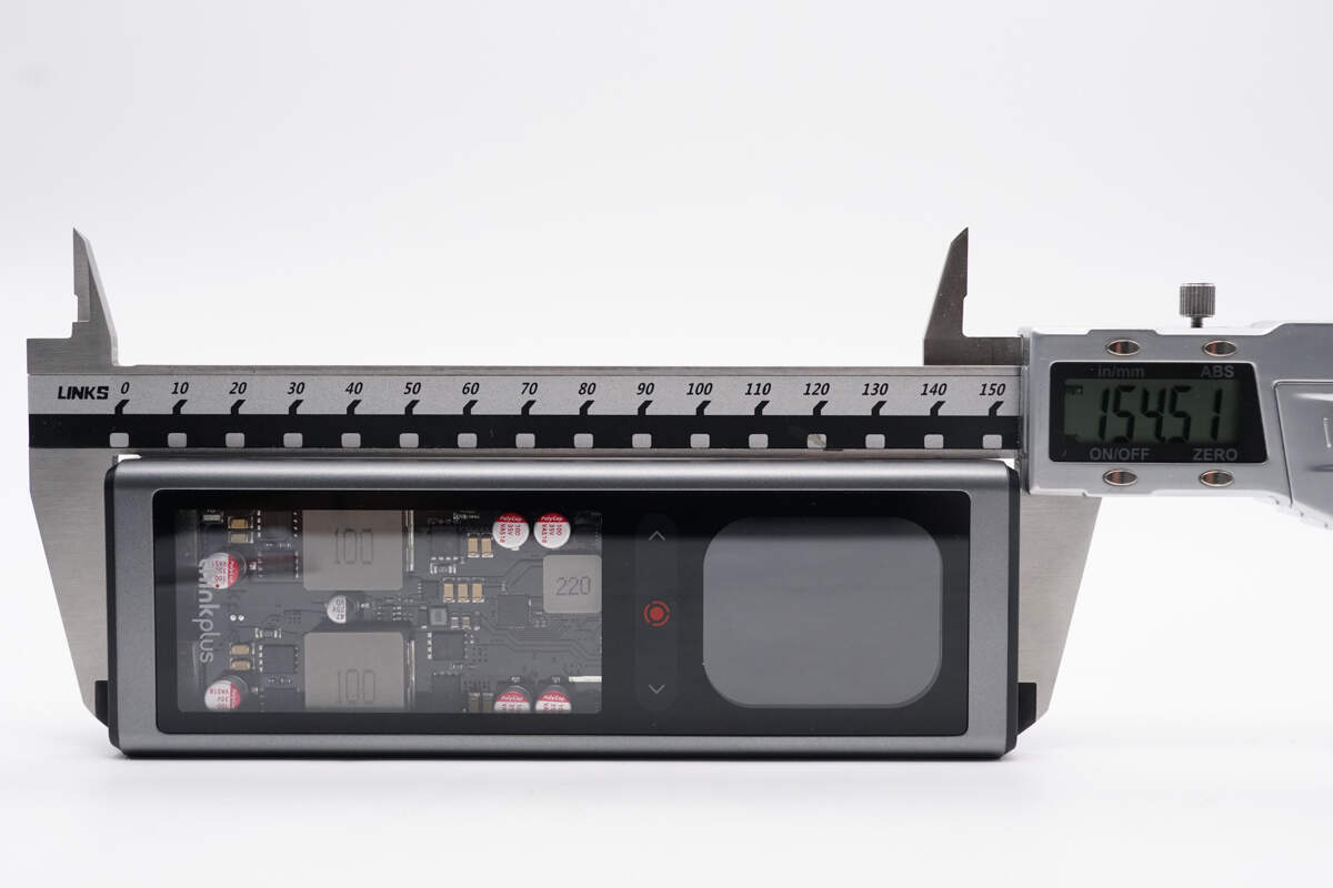
The length is about 154.51 mm (6.083 inches).
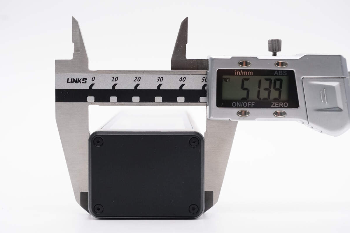
The width is about 51.39 mm (2.023 inches).
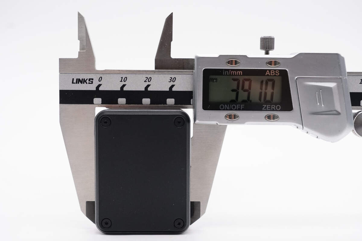
The thickness is about 39.1 mm (1.54 inches).
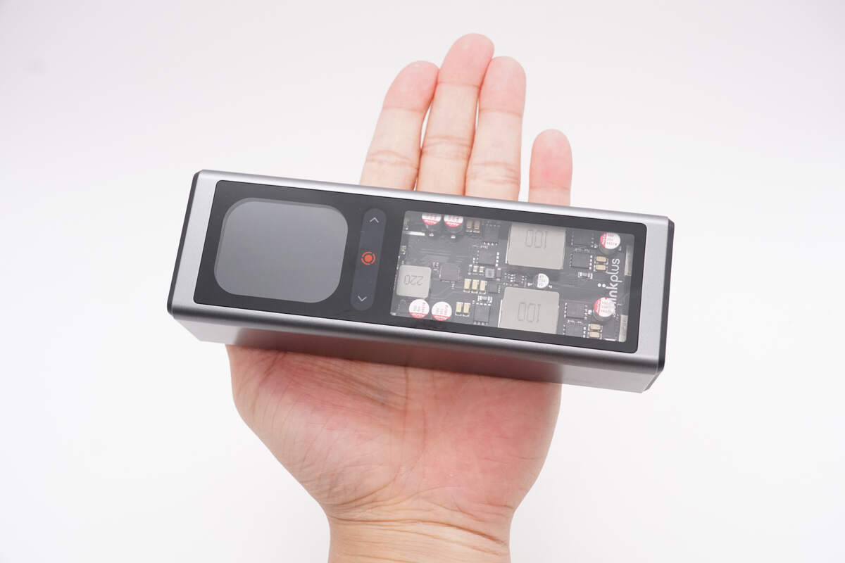
That's how big it is in the hand.
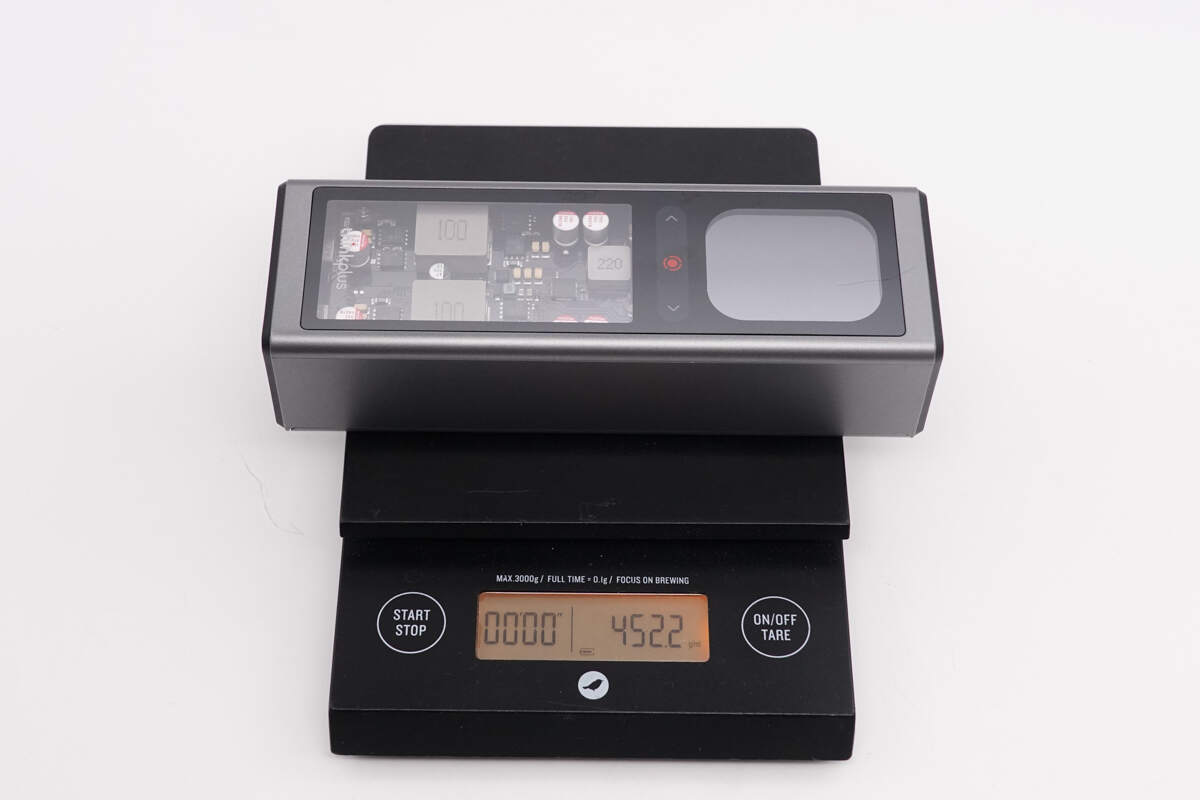
The weight is about 452 g (15.94 oz).
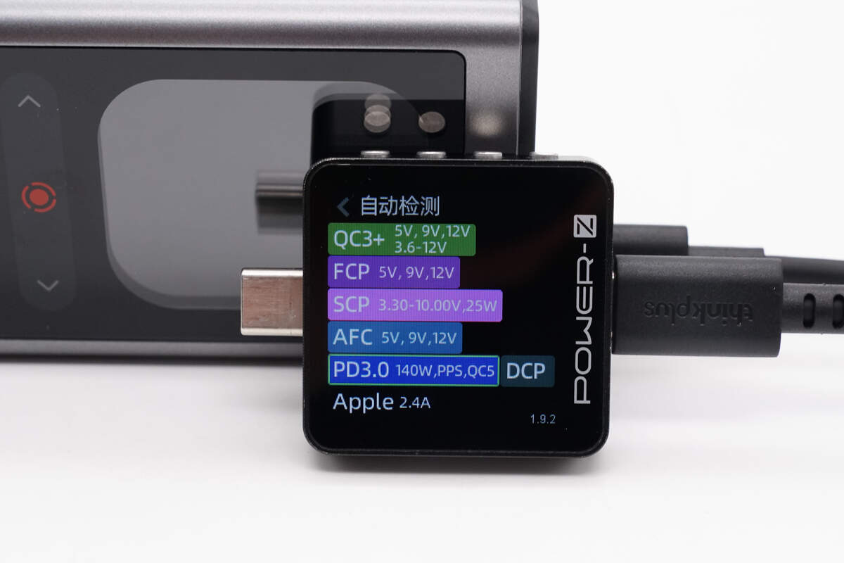
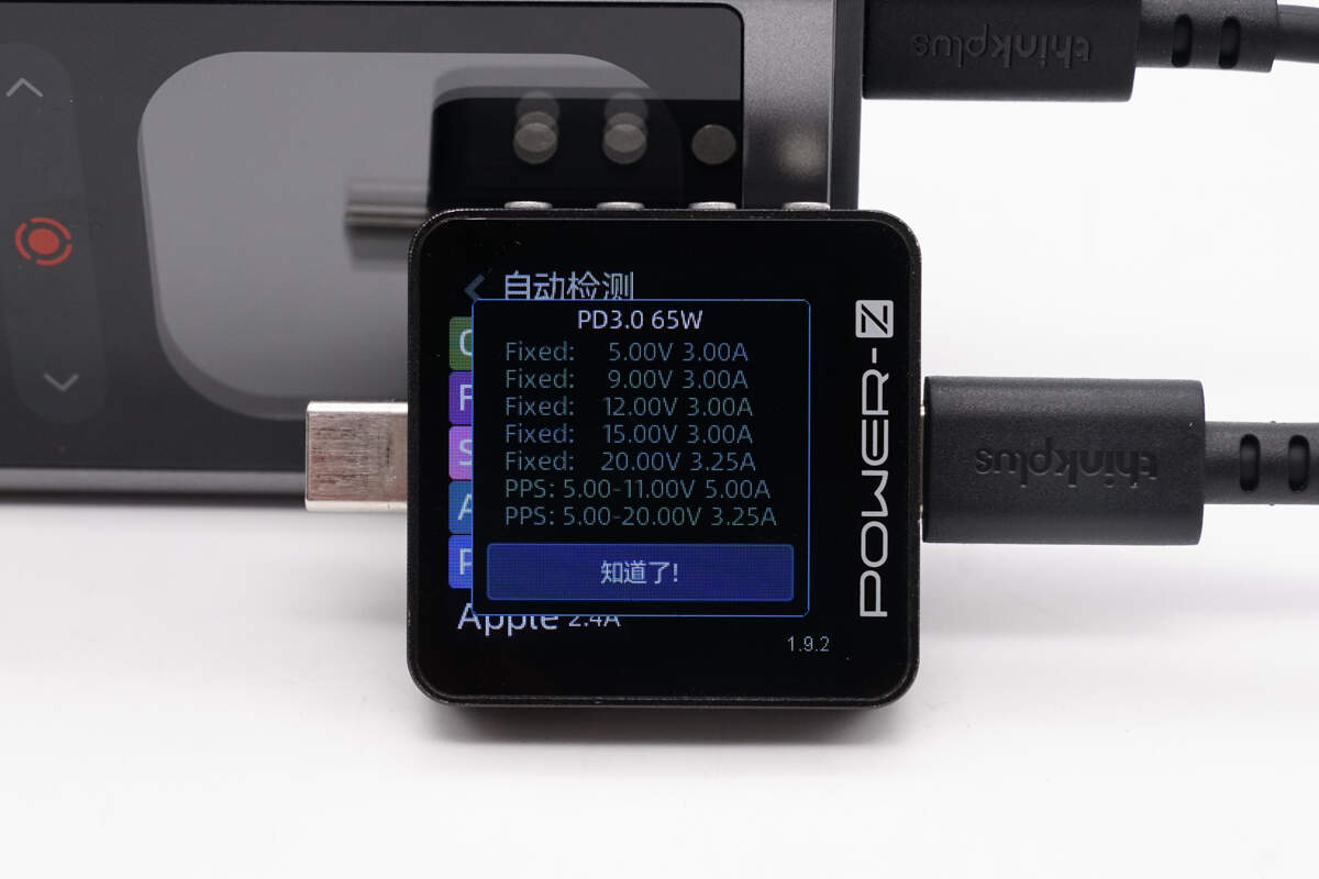
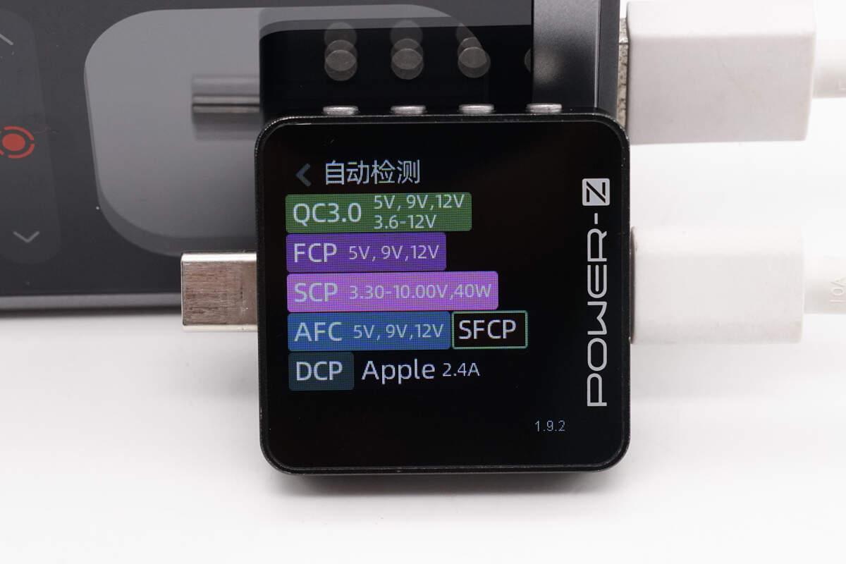
ChargerLAB POWER-Z KM003C shows the USB-C1 can support QC3+/5, FCP, SCP, AFC, PD3.0, PPS, DCP, and Apple 2.4A charging protocols.
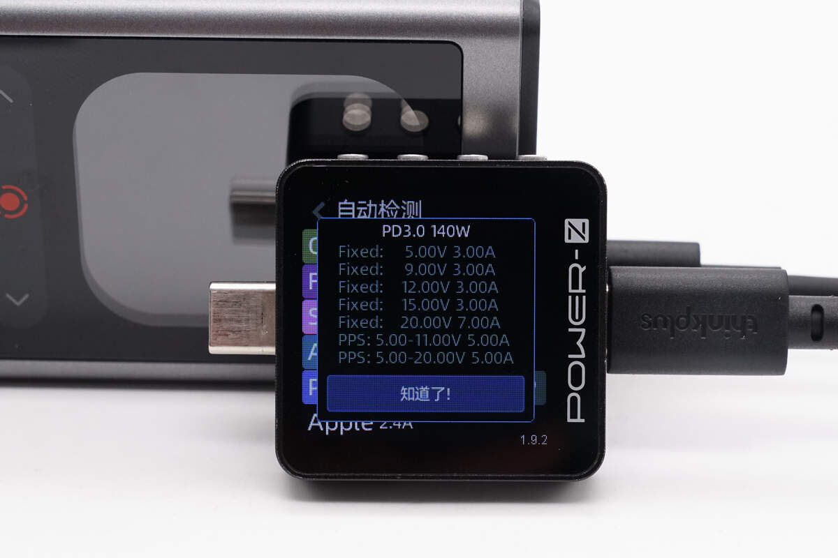
And it has five fixed PDOs of 5V3A, 9V3A, 12V3A, 15V3A, and 20V7A. It has two sets of PPS, which are 5-11V/5A and 5-20V/5A.
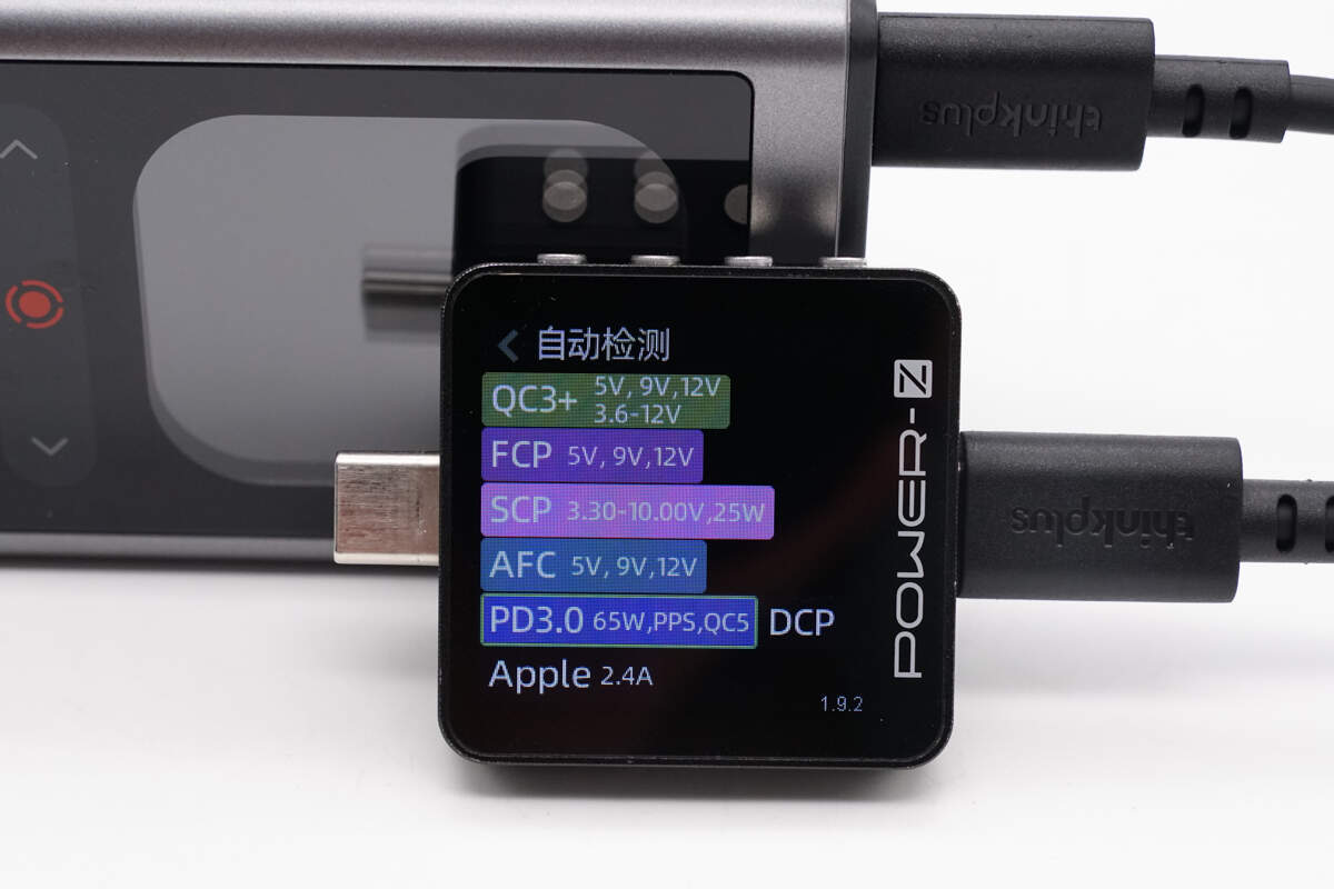
ChargerLAB POWER-Z KM003C shows the USB-C2 can support QC3+/5, FCP, SCP, AFC, PD3.0, PPS, DCP, and Apple 2.4A charging protocols.
And it has five fixed PDOs of 5V3A, 9V3A, 12V3A, 15V3A, and 20V3.25A. It has two sets of PPS, which are 5-11V/5A and 5-20V/3.25A.
The USB-A can support QC3.0, FCP, SCP, AFC, SFCP, DCP, and Apple 2.4A charging protocols.
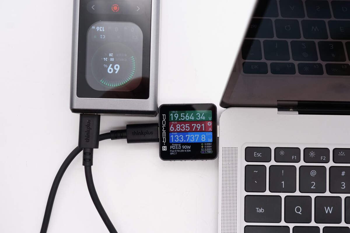
When used to charge the Huawei MateBook X Pro, the power reaches approximately 133.74W, successfully triggering 20V/7A 140W fast charging.
Teardown
Next, let's take it apart to see its internal components and structure.
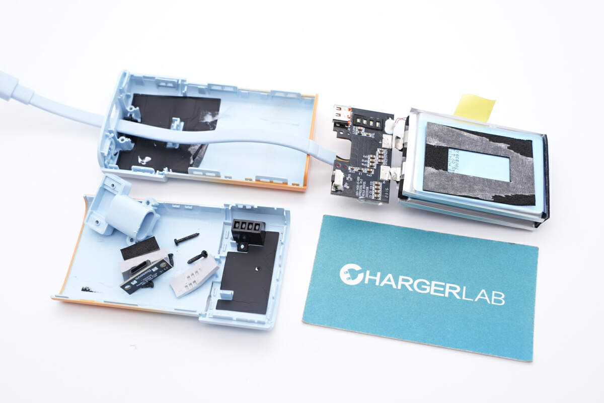
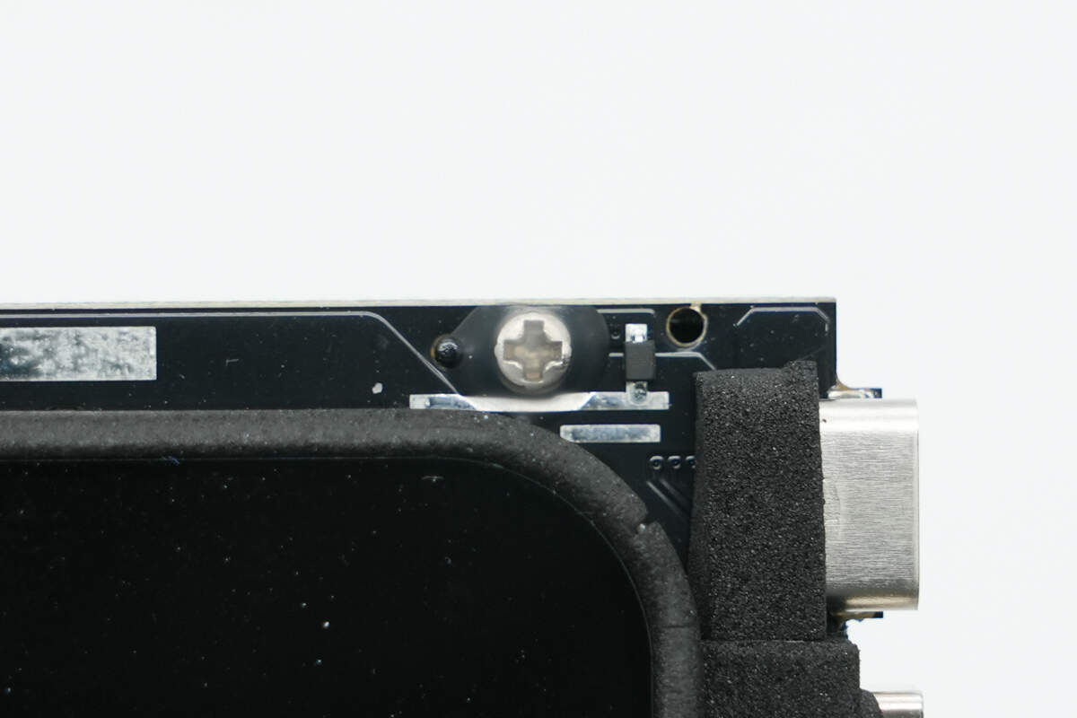
Remove the top screws to open the panel, there are two more screws inside.
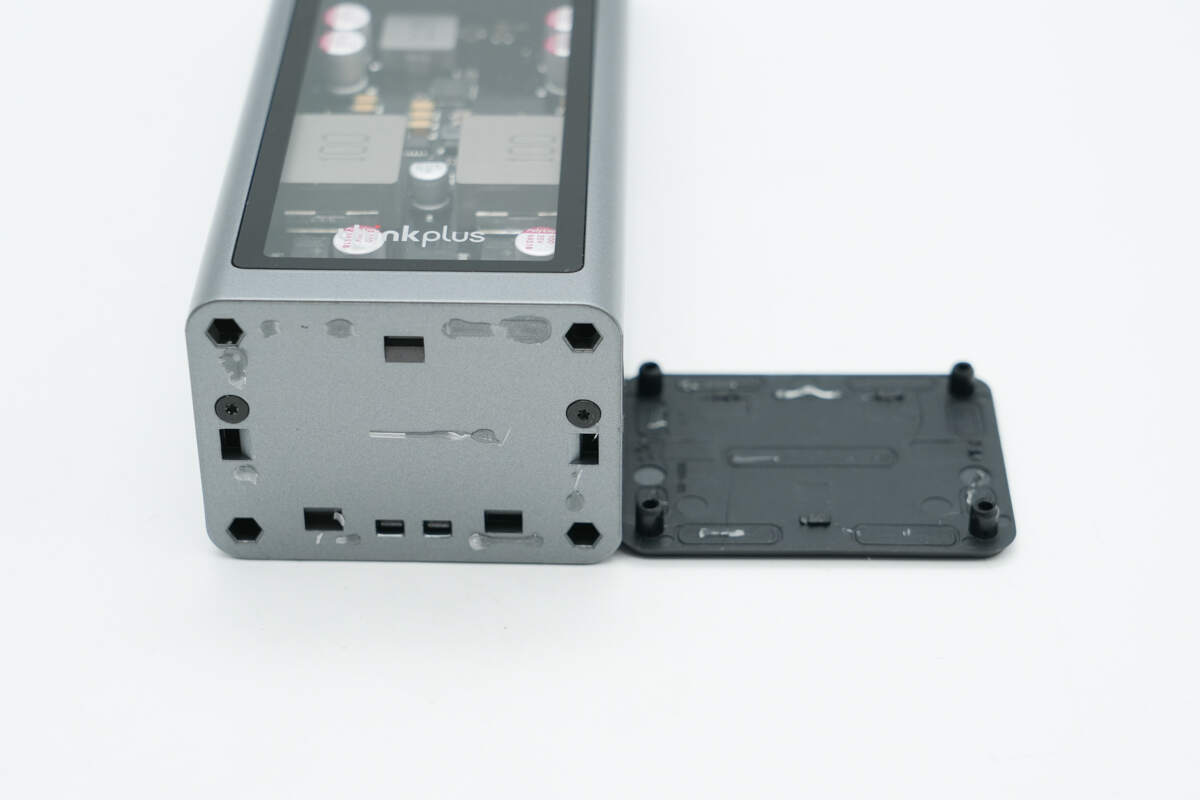
Remove the bottom cover as well, there are also two additional screws inside.
Unlike other drawer-style designs for power banks, this one secures the module with screws at both ends. To remove the module, the casing must be cut open.
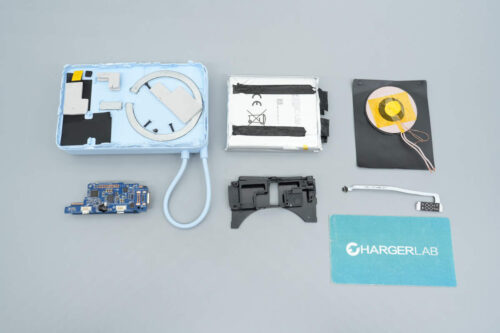
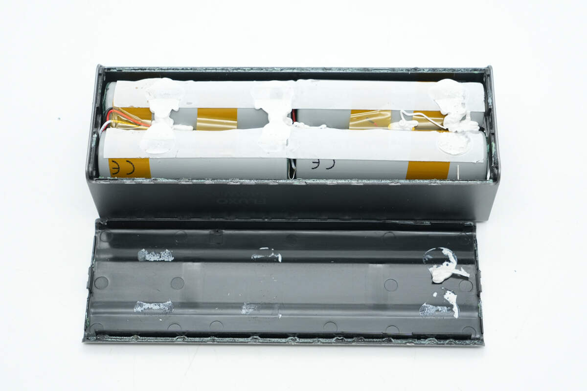
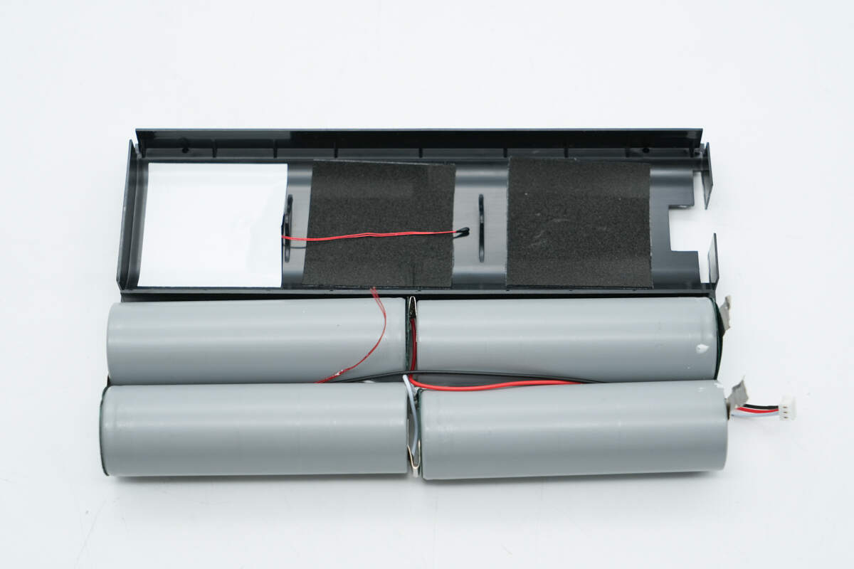
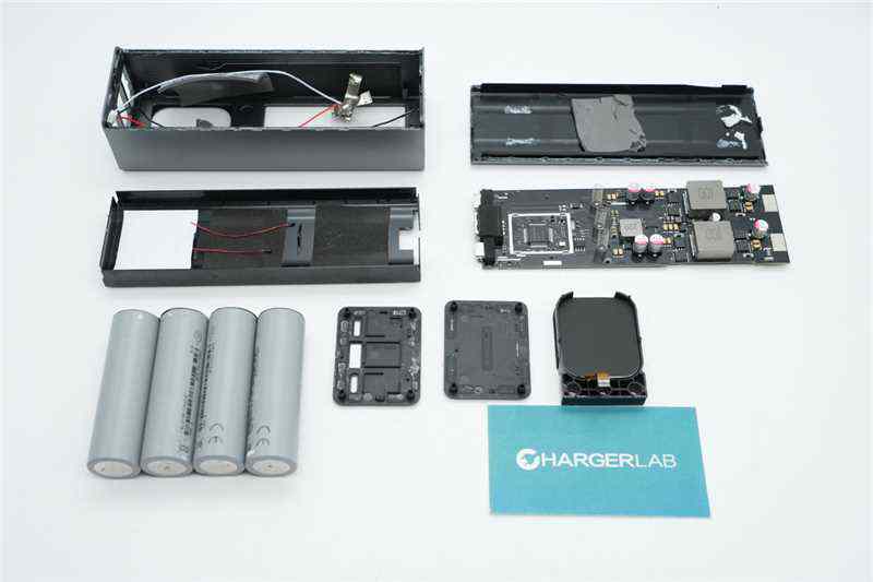
After removing the back cover, take out the internal module.
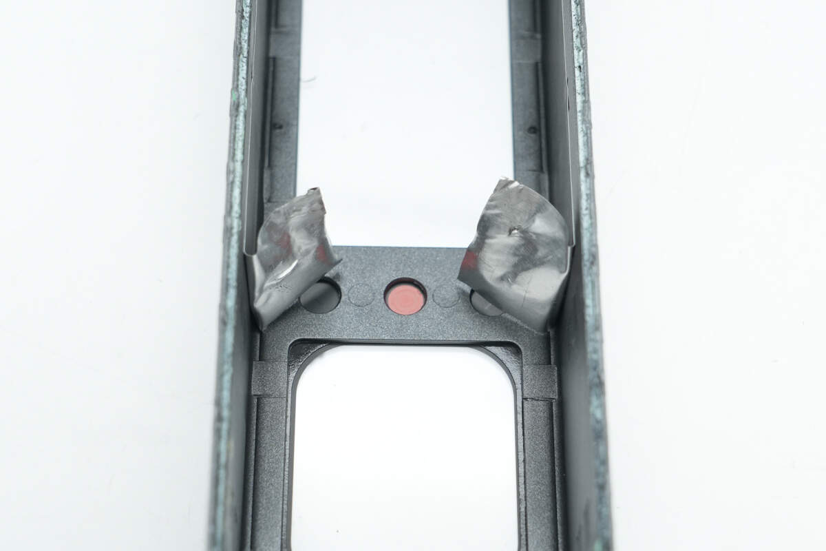
The inner sides of the casing are lined with heat-dissipating aluminum foil, which has been insulated.
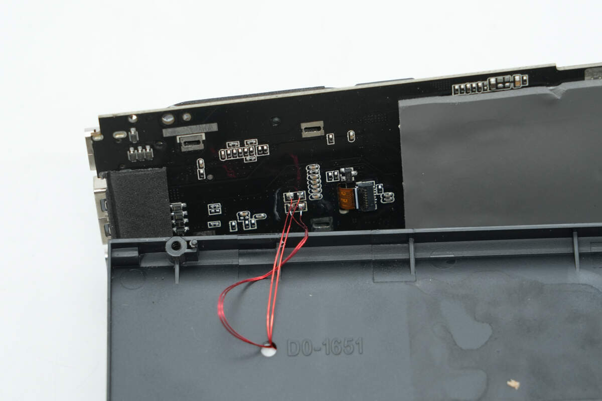
The PCB is positioned above the battery pack and secured with screws.
The screws are reinforced with adhesive.
The battery pack's positive and negative terminals are connected to the PCB via spot-welded nickel strips and plug-in wires.
A plastic plate is used to separate the PCB and the battery pack.
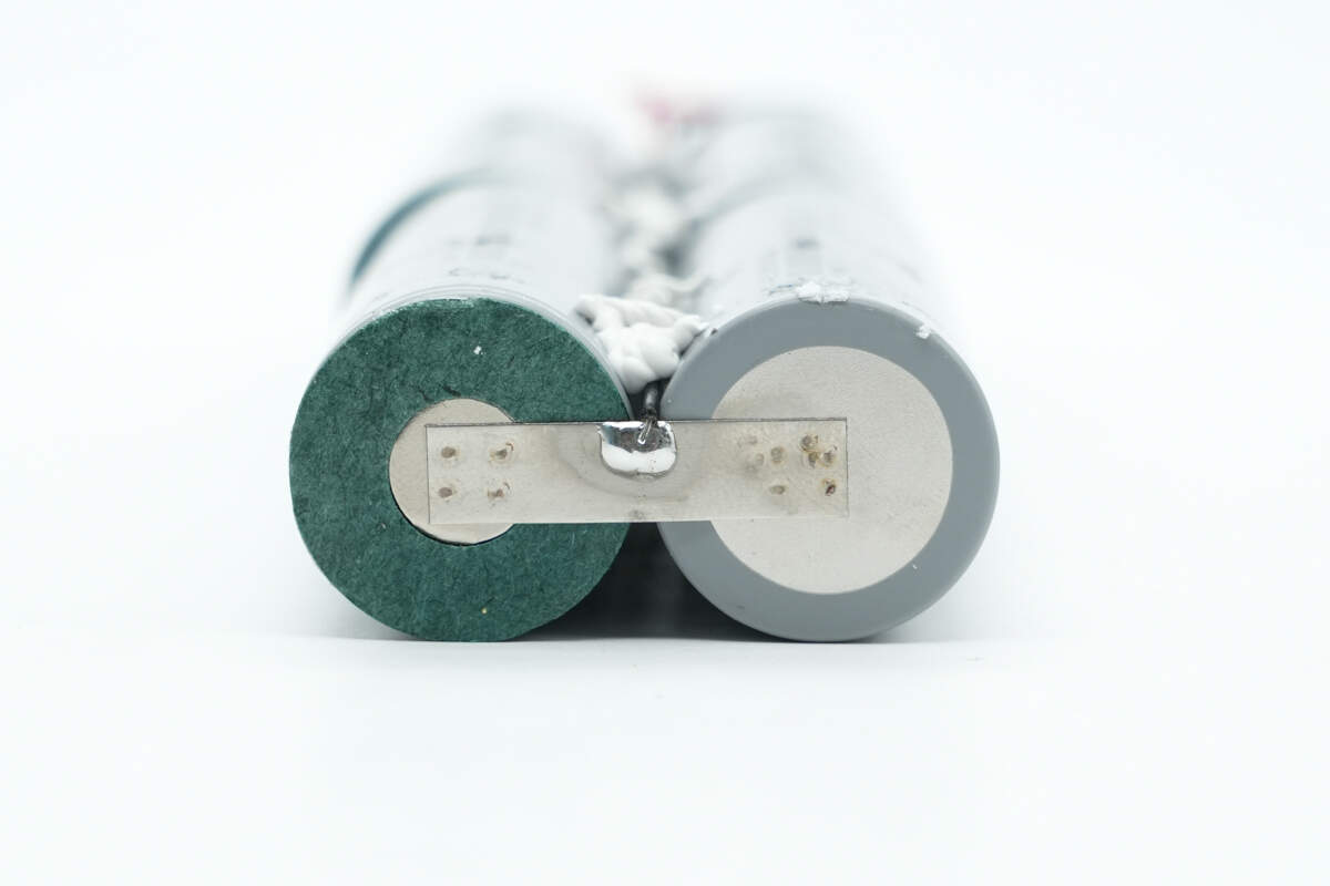
Separate the PCB and the battery pack, the thermistor passes through a hole in the isolation plate to monitor the cell temperature.
The thermistor is secured with tape.
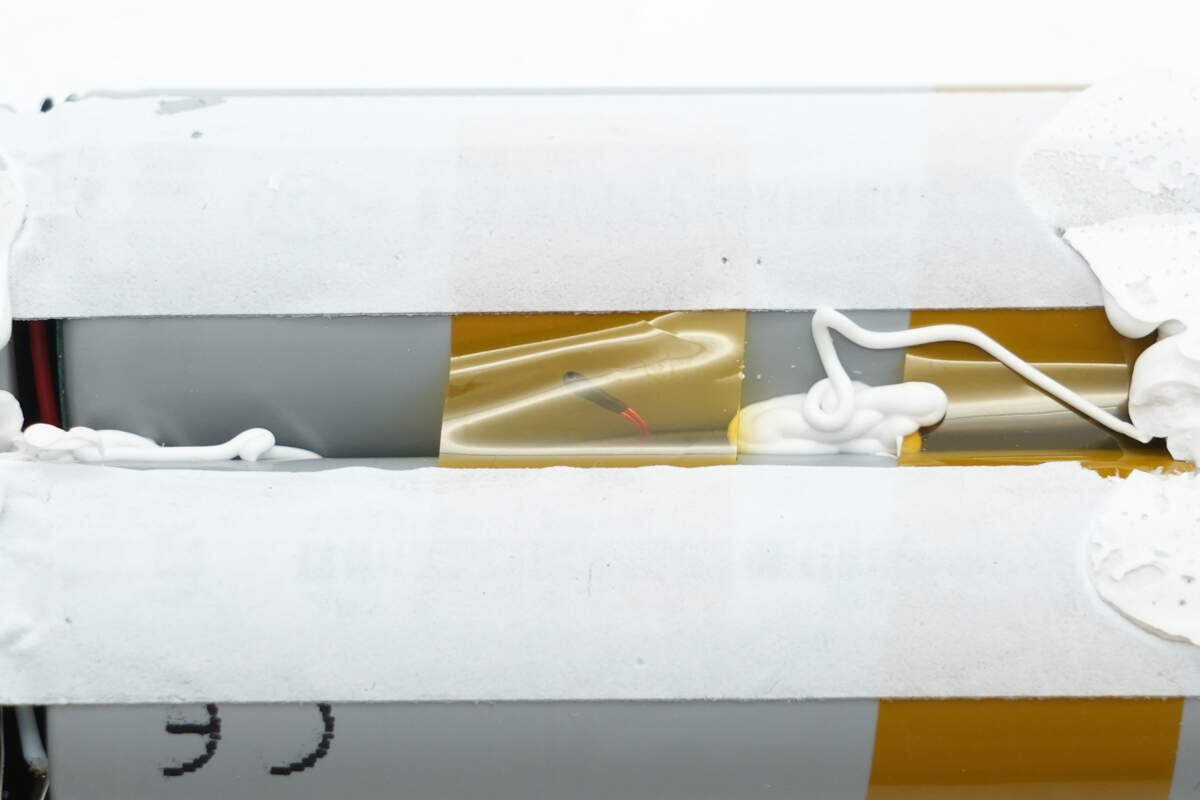
After removing the battery cells, you’ll find cushioning foam attached inside the groove of the plastic isolation plate.
The battery cells are connected by spot-welded nickel strips, with the positive terminals covered by oiled paper.
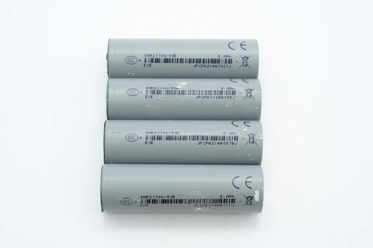
All four battery cells have the same part number, come from EVE, and have passed CCC and CE certifications.
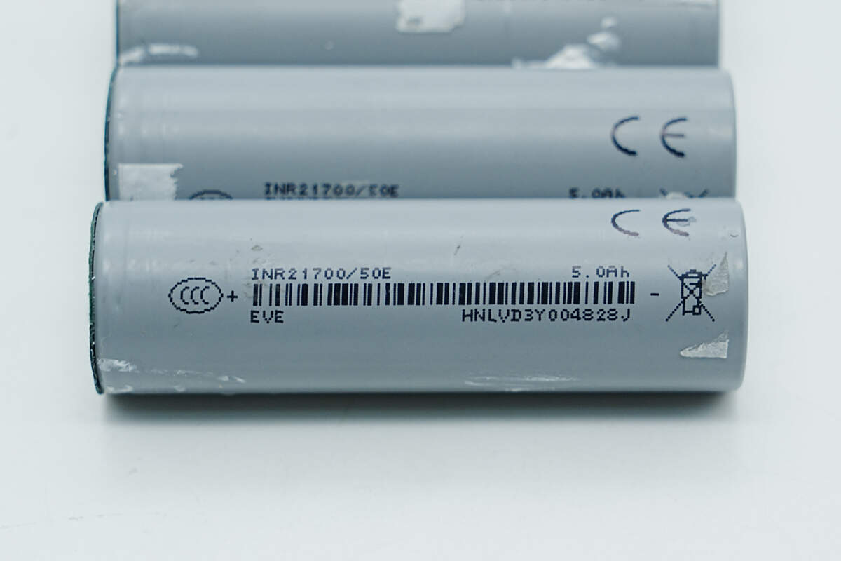
The 21700 battery model is INR21700/50E, with a capacity of 5Ah, and is an automotive-grade cell.
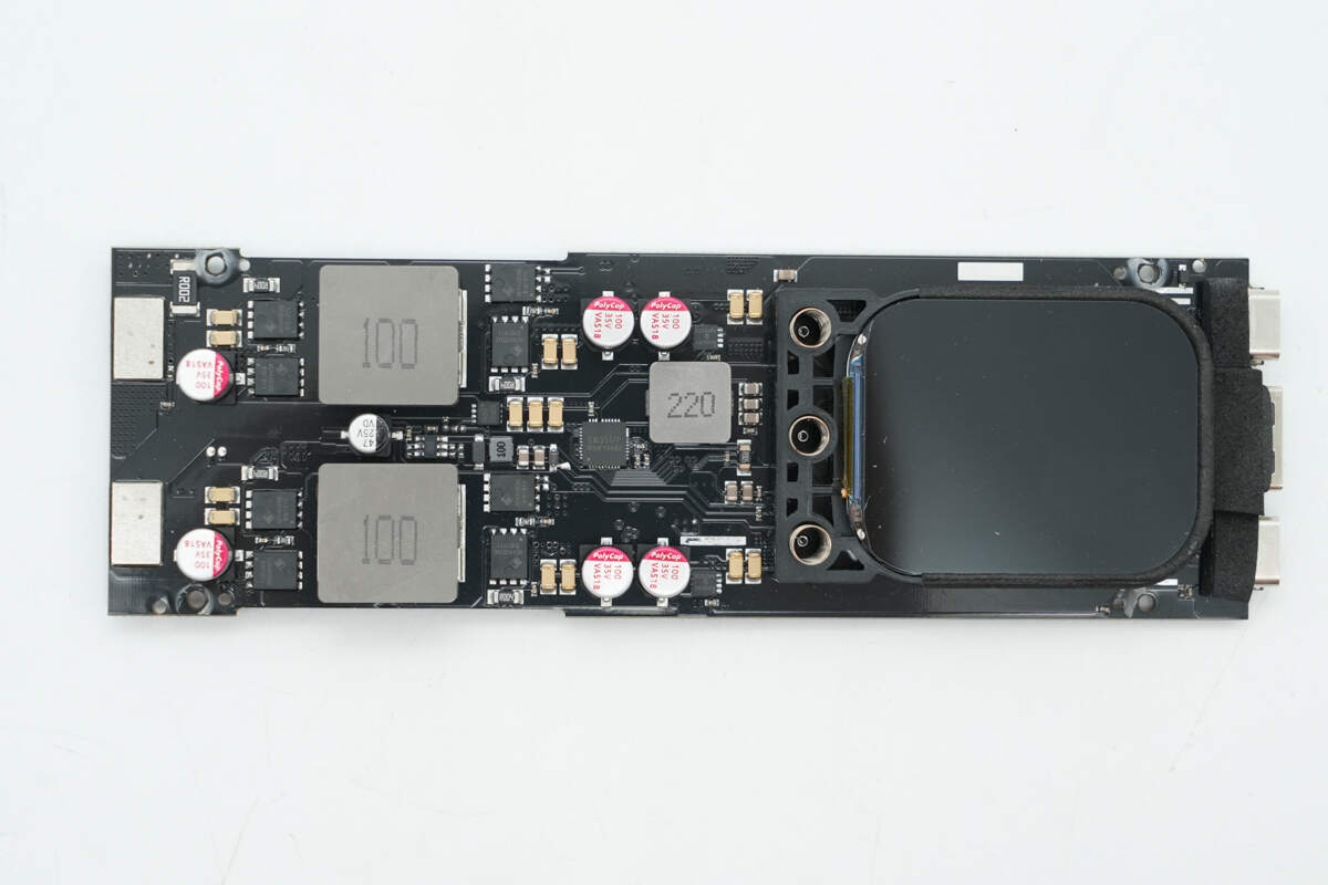
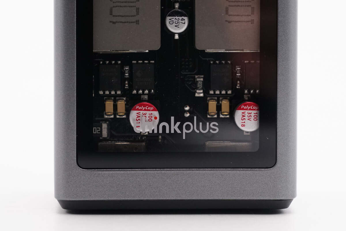
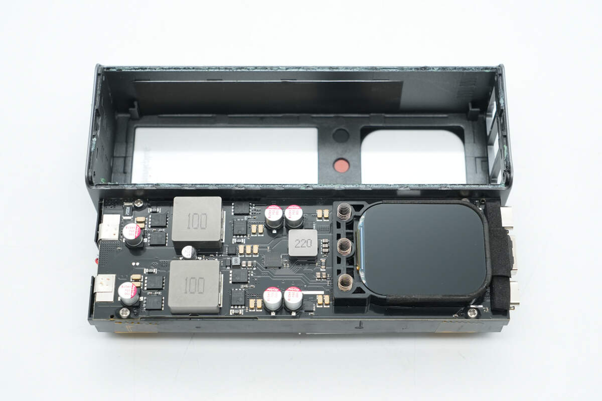
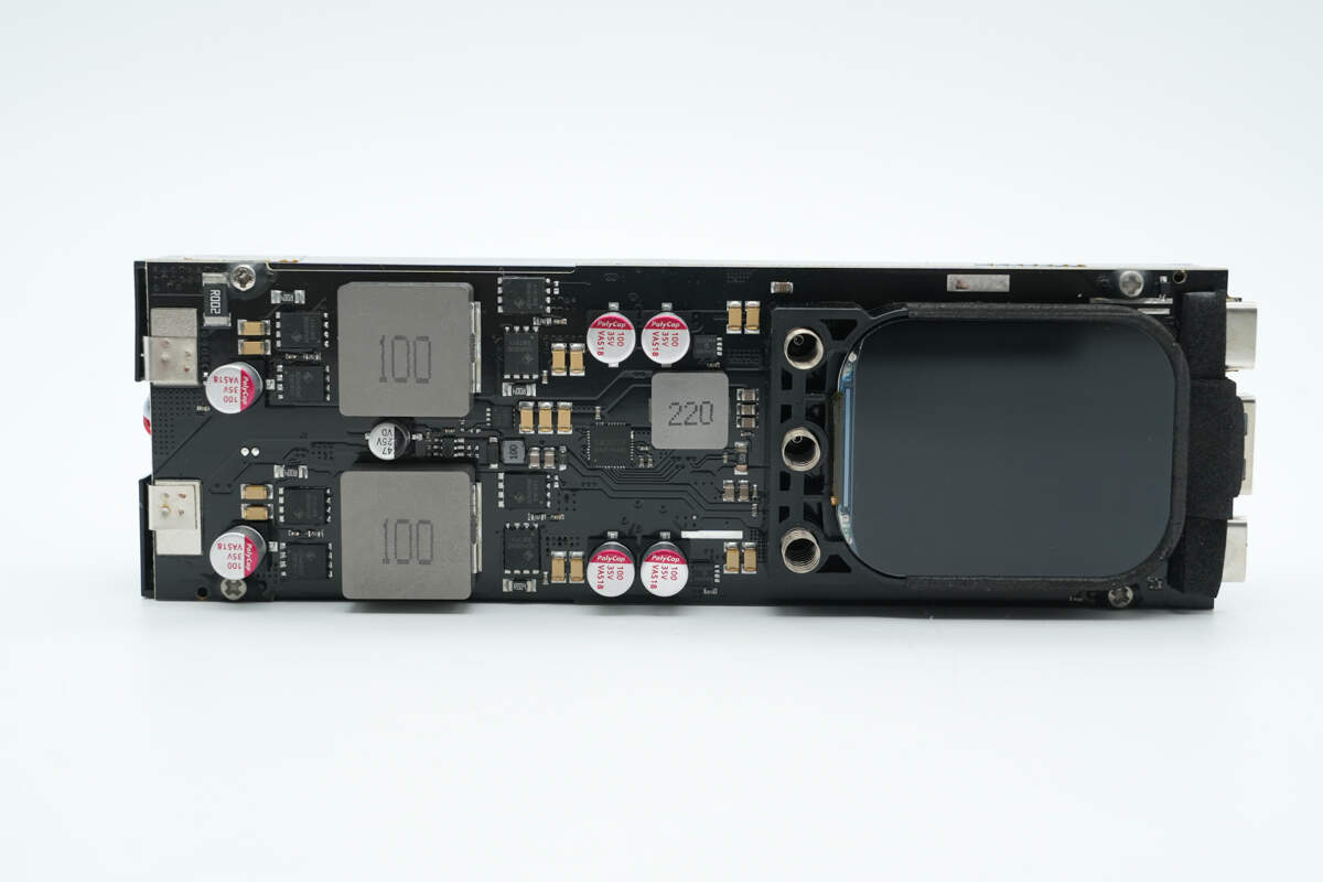
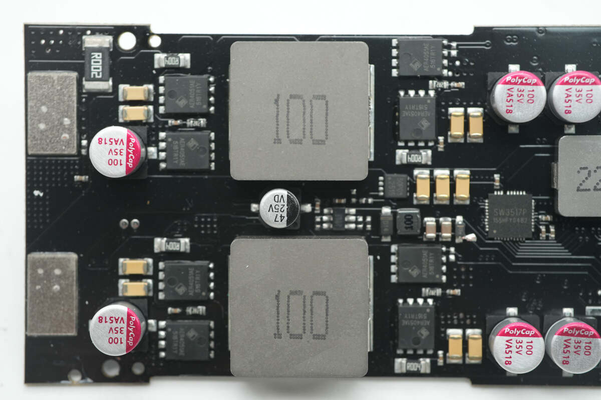
On the front left side of the PCB, two USB-C bidirectional buck-boost circuits are arranged vertically, each accompanied by inductors, buck-boost MOSFETs, solid capacitors, and VBUS MOSFETs.
In the central area, there is a buck protocol chip for the USB-A output step-down circuit, a buck inductor, and related components for the step-down circuit that powers the MCU. On the right side is the screen, supported by a plastic plate, with three sets of springs corresponding to the touch buttons.
After removing the screen module, you’ll find the MCU, memory chip, touch controller, and the VBUS MOSFET for the USB-A port inside.
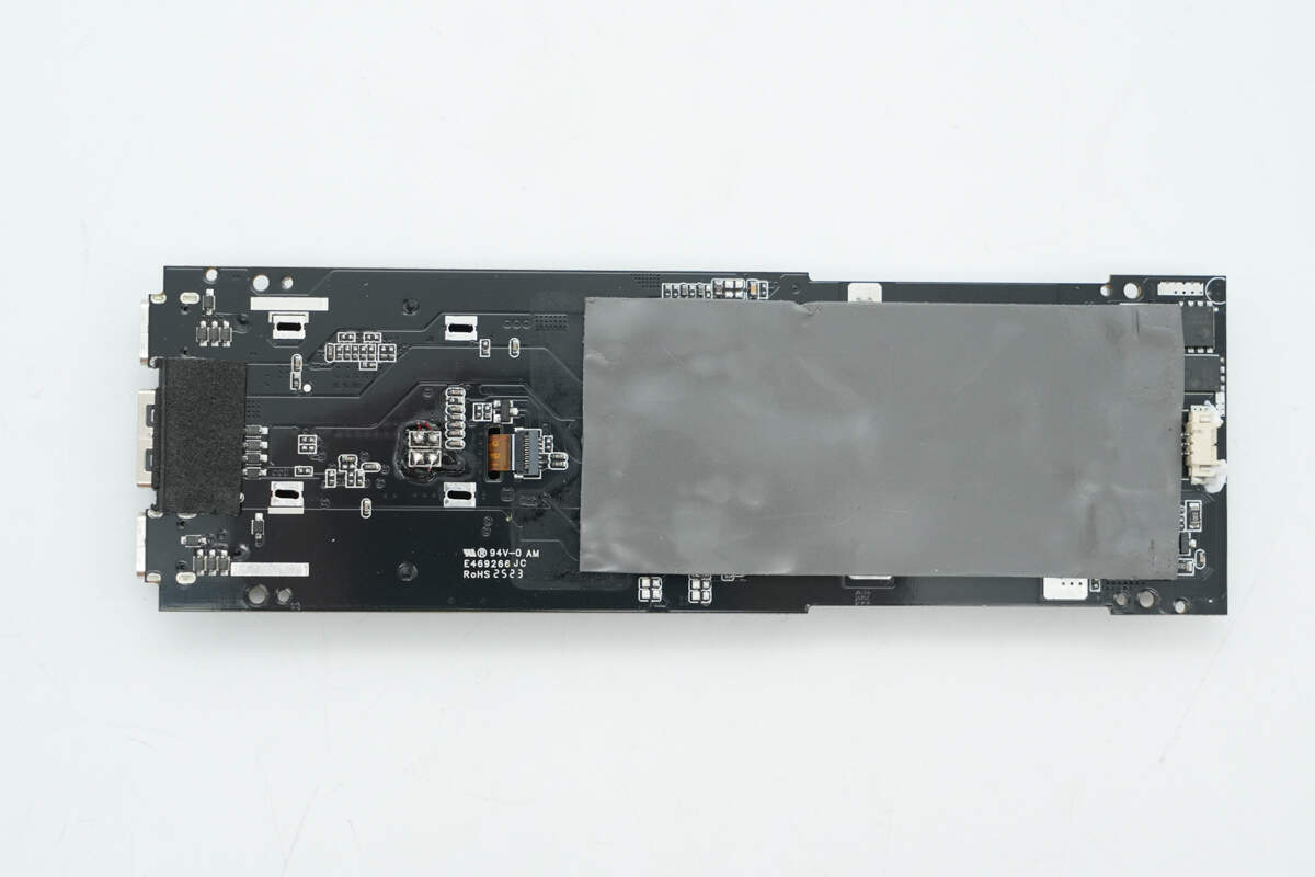
The back of the PCB is covered with a thermal pad.
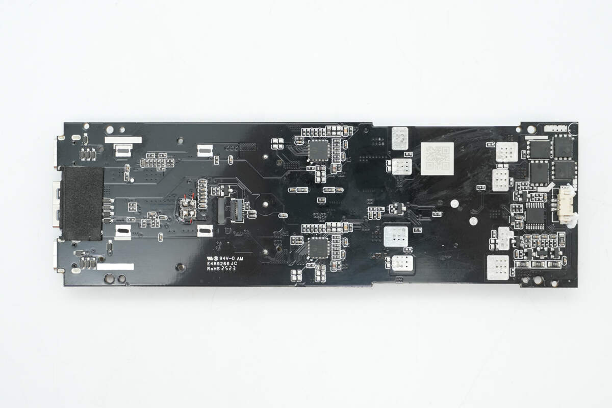
After removing the thermal pad, you’ll see a lithium battery protection chip and protection MOSFET on the right side, with two USB-C power management chips located in the middle.
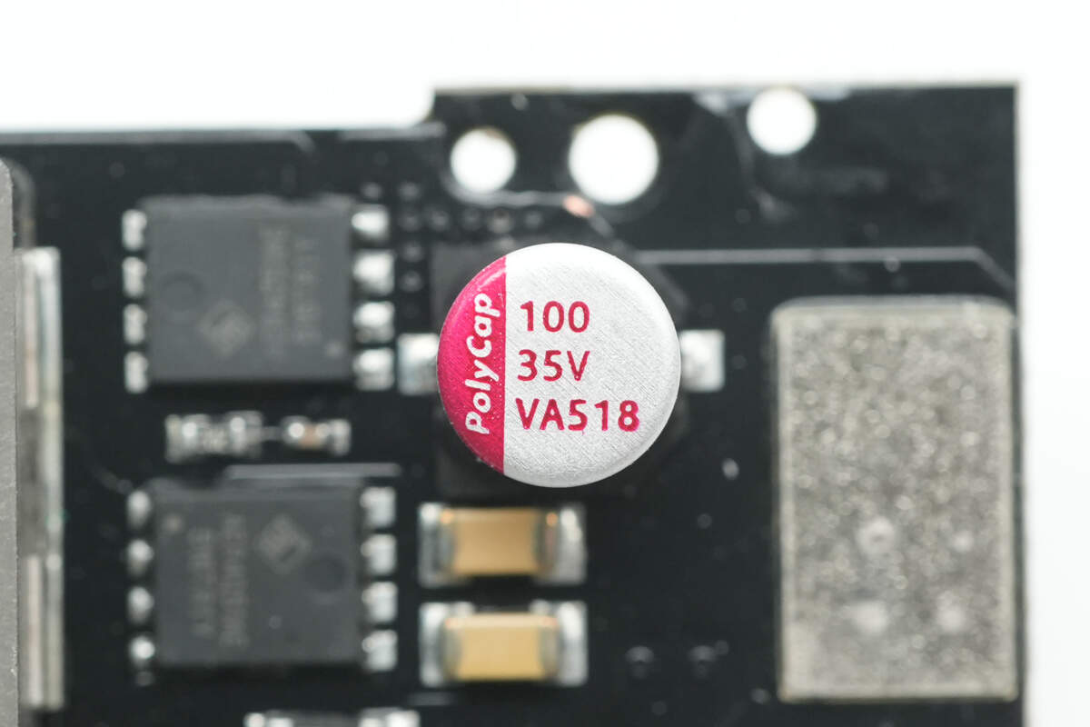
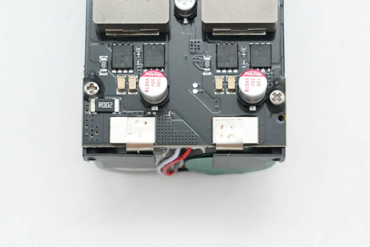
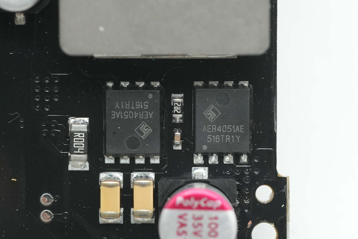
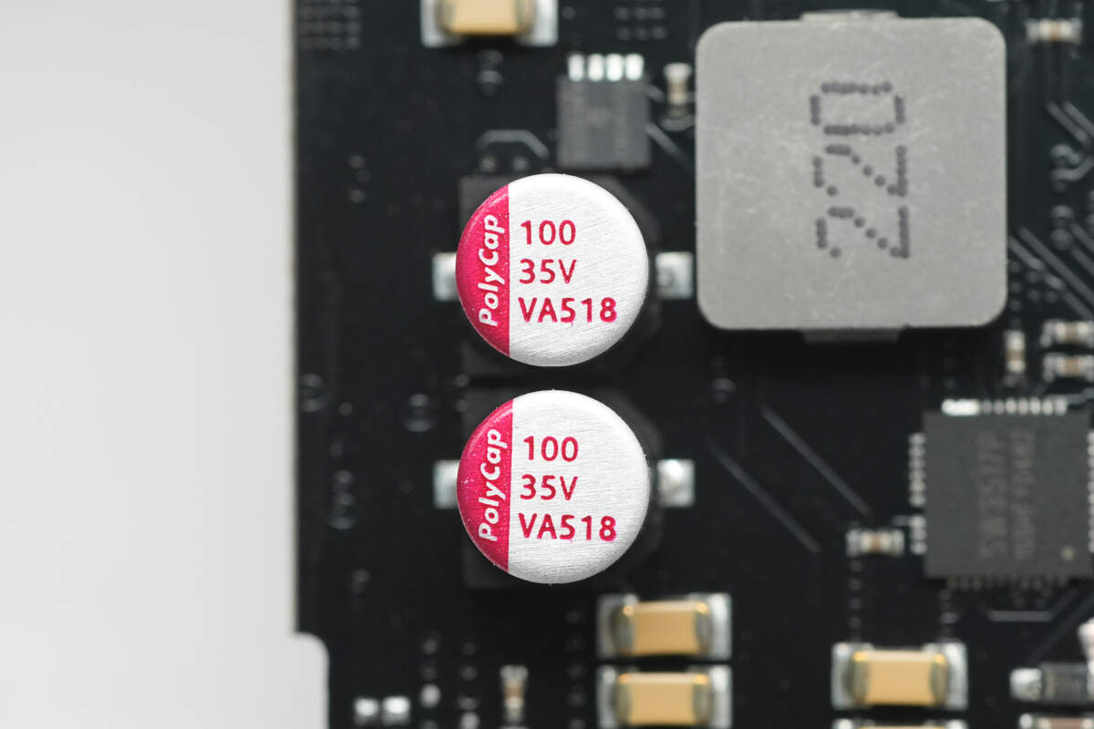
The two solid capacitors at the battery side are from PolyCap, each rated at 35V 100μF.
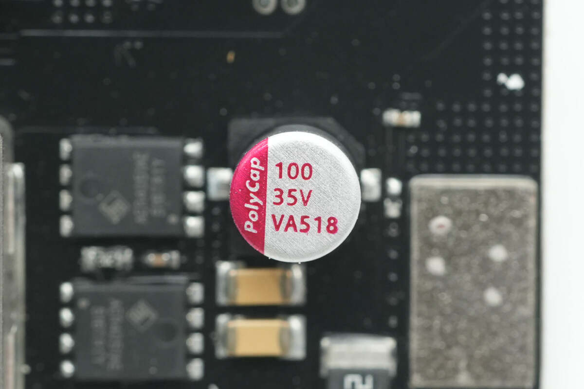
A close-up of the other solid capacitor.
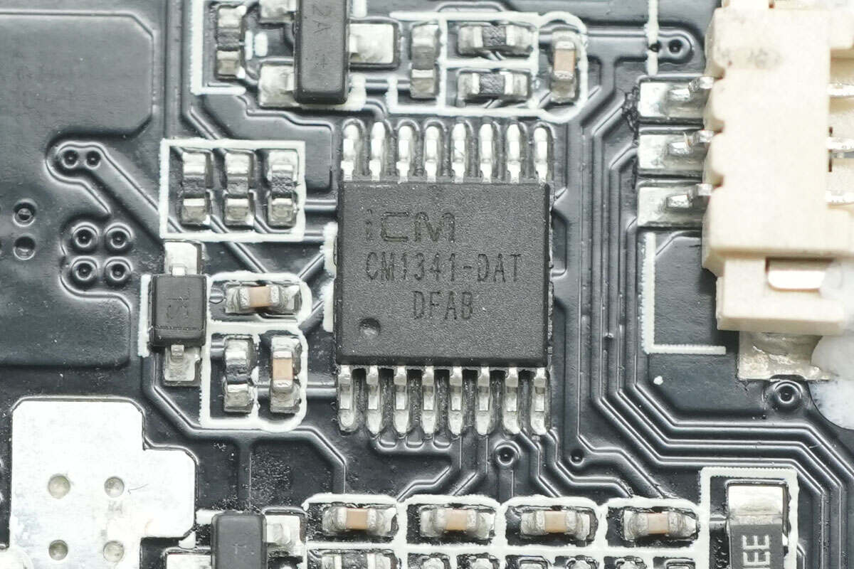
The battery protection chip is from iCM, model CM1341-DAT. It is specifically designed for 4-series lithium-ion or lithium iron phosphate batteries and features built-in high-precision voltage and current detection circuits. By monitoring the voltage of each cell, charge/discharge current, and temperature, it provides multiple protections including overcharge, overdischarge, balancing, open circuit, low-voltage charge prohibition, discharge overcurrent, short circuit, charge overcurrent, and overtemperature protection. The discharge overcurrent protection delay is adjustable via an external capacitor, while other protection delays are built-in.
The iCM CM1341-DAT offers 15mV overcharge detection accuracy, supports three-level discharge overcurrent protection, charge overcurrent protection, cell wiring disconnection detection, and NTC thermistor disconnection protection, providing comprehensive protection for multi-cell lithium battery packs.
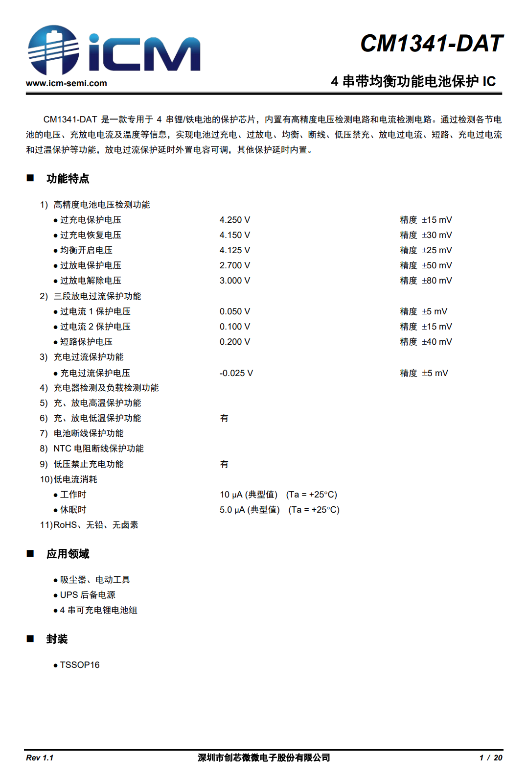
The battery protection MOSFET is an ALLEPIC AER4051AE, an NMOS with a 40V rating and 5.5mΩ on-resistance, packaged in PDFN5060.
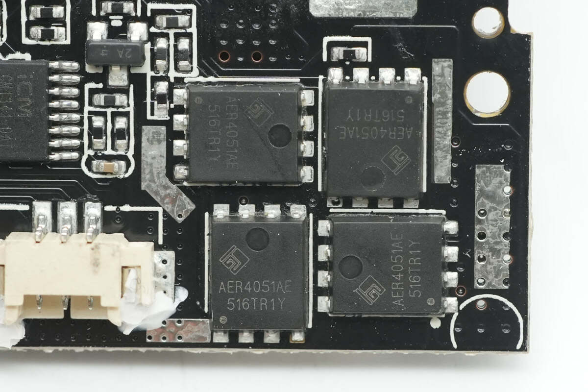
Both USB-C power management chips are Injoinic IP2366 models.
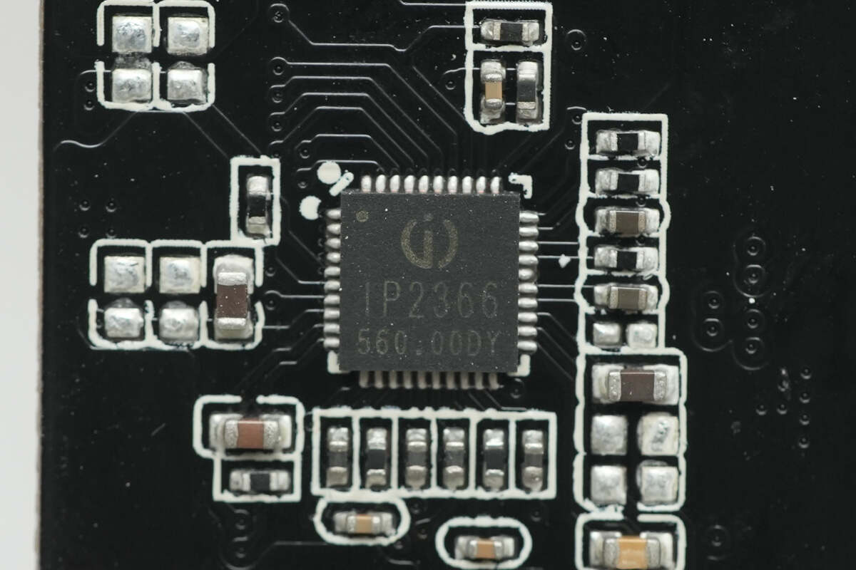
The Injoinic IP2366 is a lithium battery charge-discharge management chip integrating PD 3.1 and multiple fast-charging protocols with a bidirectional synchronous buck-boost converter, supporting up to 140W power. It features high integration and rich functions, requiring only one inductor for synchronous buck-boost operation and minimal external components, effectively reducing overall size and BOM cost.

The IP2366 supports 2 to 6 series battery cells and allows setting the cell count and battery type via external resistors. It supports full charge voltages of 3.65V, 4.1V, 4.2V, 4.35V, and 4.4V. The chip has built-in temperature and input voltage monitoring loops, intelligently adjusting charging current based on detected charger power.
It features a low-power mode with a standby current as low as 5μA. When a charger is plugged in, it automatically wakes up to charge; discharging requires a short button press to wake. The built-in 14-bit ADC precisely measures input voltage/current and battery voltage/current, with data accessible via I²C.
Packaged in a 5×5mm QFN40 (0.4mm pitch), the IP2366 provides multiple protections, including input overvoltage/undervoltage, output overcurrent/short circuit, battery overcharge/overdischarge/overcurrent, chip overtemperature, and NTC temperature protection. CC1/CC2 pins support 30V tolerance to prevent damage, ensuring high reliability.
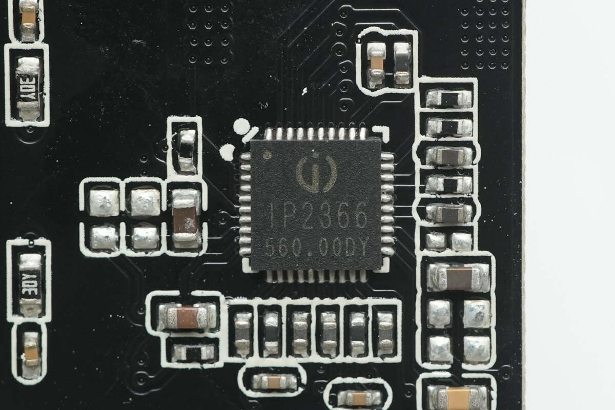
Here’s a close-up of the other Injoinic IP2366 chip.
The two synchronous buck-boost circuits use identical designs, each paired with a 10μH alloy inductor. Both sides also feature two synchronous buck-boost MOSFETs.
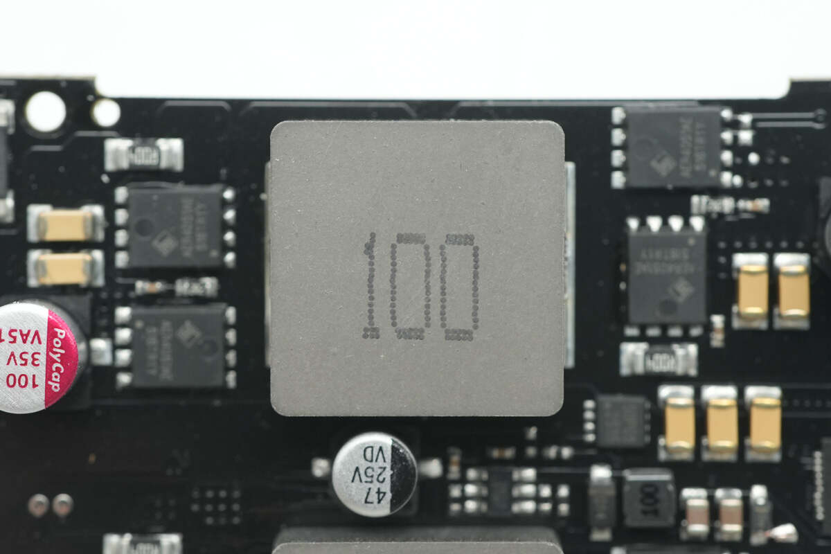
The alloy inductors are integrated Fe-Si-Al molded surface-mount types, offering stronger overcurrent capability compared to regular inductors.
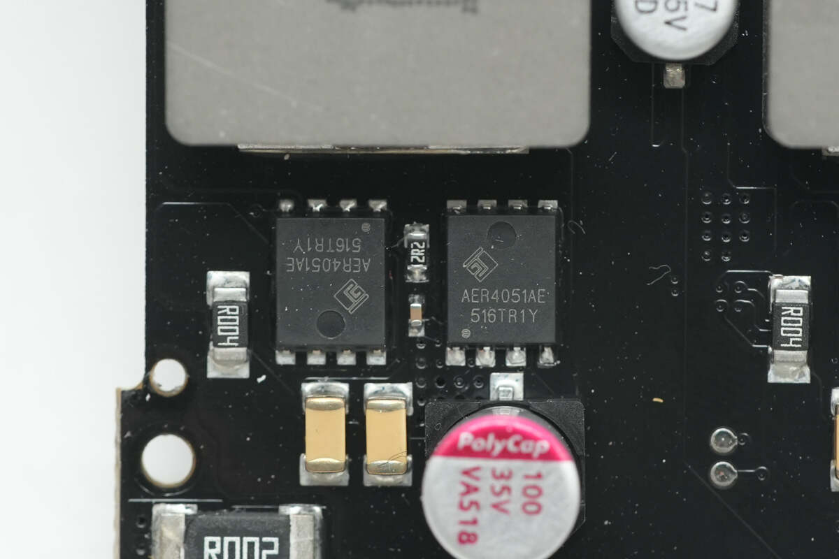
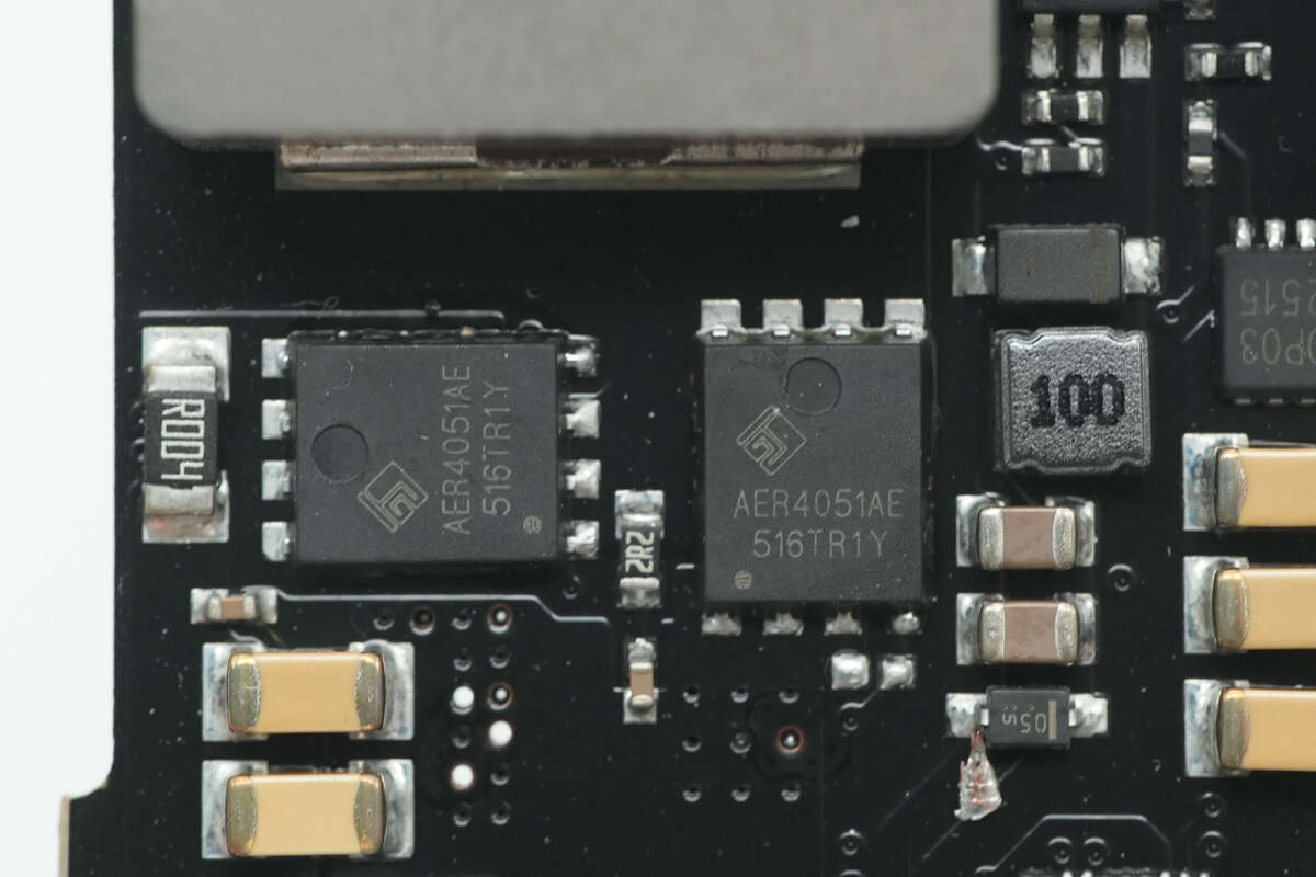
All eight synchronous buck-boost MOSFETs in the two buck-boost circuits are also ALLEPIC AER4051AE models.
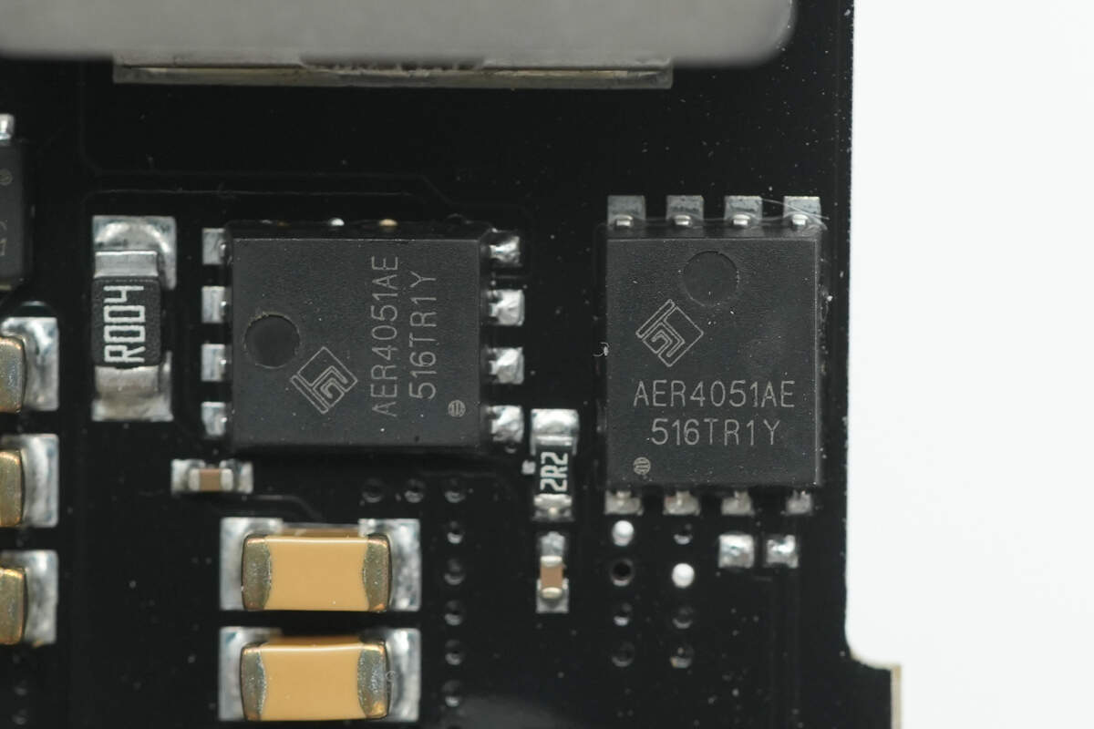
Here’s a close-up of the other two ALLEPIC AER4051AE MOSFETs on the opposite side.
A close-up of the two ALLEPIC AER4051AE synchronous buck-boost MOSFETs in the other buck-boost circuit.
Here’s a close-up of the other two ALLEPIC AER4051AE MOSFETs.
These two solid capacitors are also from PolyCap, each rated at 35V 100μF.
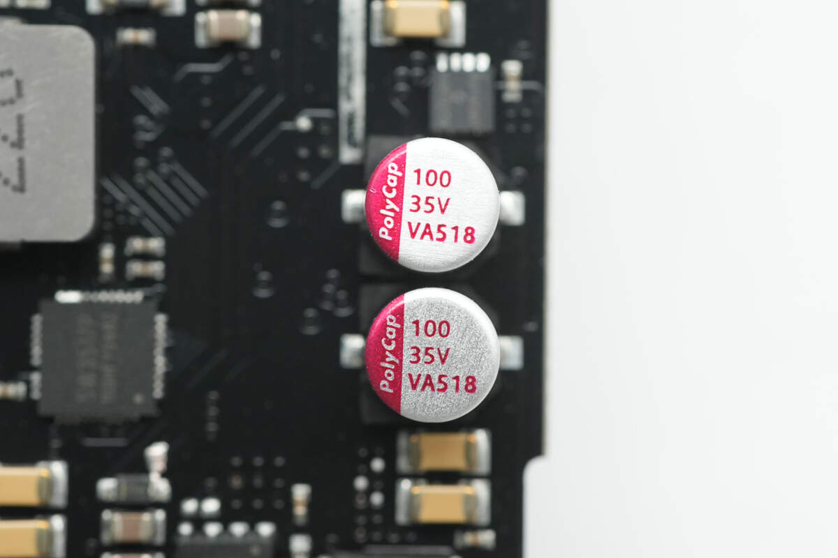
Here’s a close-up of the other pair of solid capacitors, with the same part number.
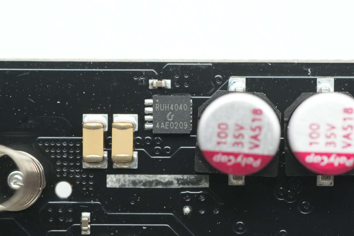
The USB-C1 VBUS MOSFET is from Ruichips, model RUH4040M2. It is an NMOS transistor with a 40V rating, 5mΩ on-resistance, and comes in a PDFN3333 package.

The USB-C2 VBUS MOSFET is also a Ruichips RUH4040M2.
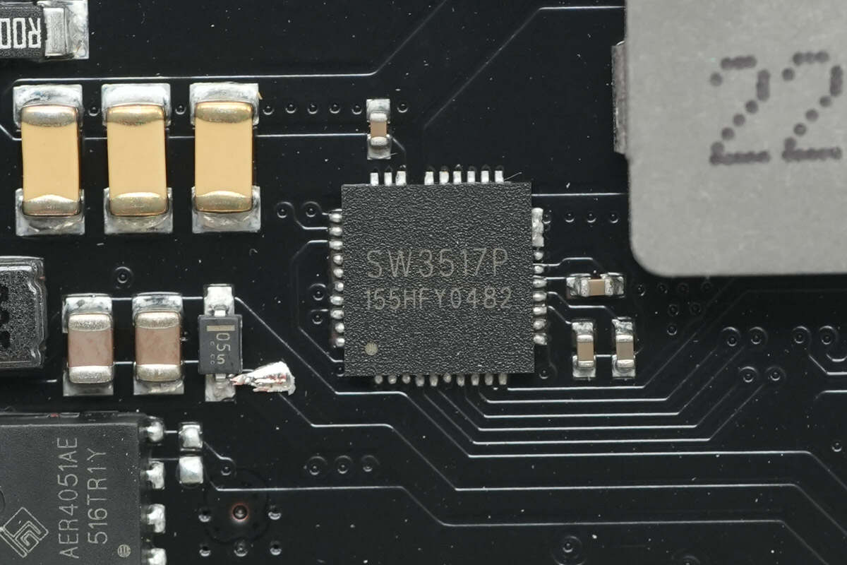
The USB-A port’s buck protocol chip is the iSmartWare SW3517P, a highly integrated dual-port charging chip supporting fast charging on either A or C port with independent current limits. It features a 5A high-efficiency synchronous buck converter and supports multiple fast-charge protocols including PPS, PD, QC, AFC, FCP, SCP, PE, and SFCP, along with CC/CV modes and dual-port management logic. With minimal external components, it forms a complete, high-performance multi-protocol dual-port charging solution.
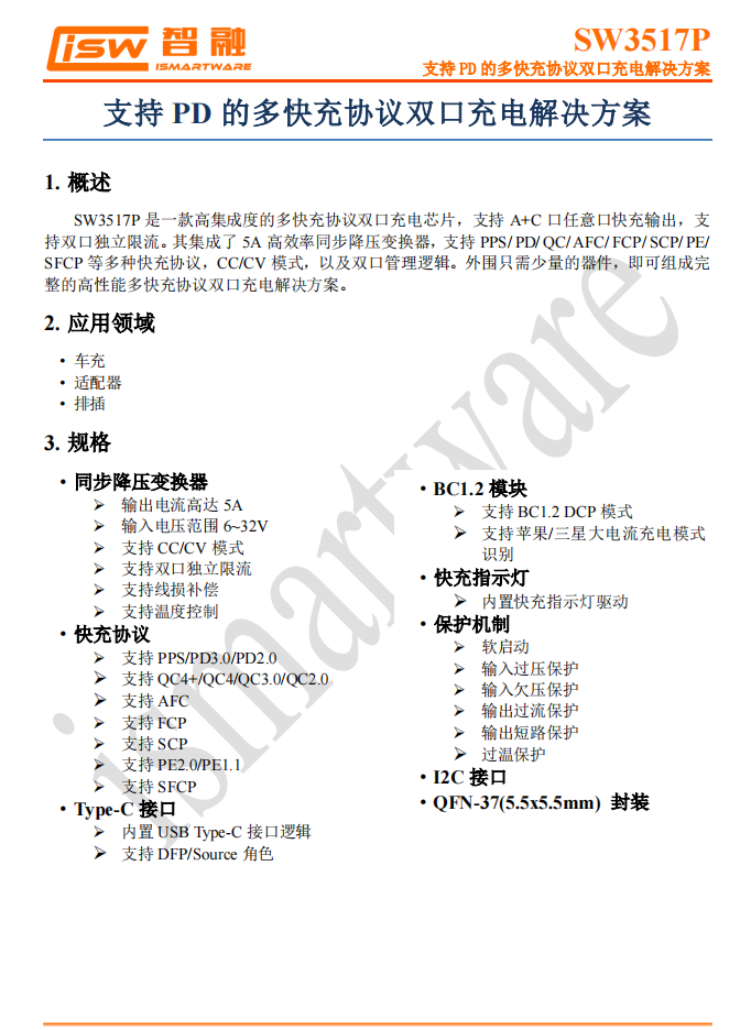
Here is the information about iSmartWare SW3517P.
The alloy inductor paired with the iSmartWare SW3517P is rated at 22μH.

The USB-A port VBUS MOSFET is also a Ruichips RUH4040M2.
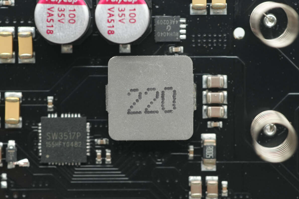
One of the buck chips is from SCT, model SCT2613. It is a high-efficiency synchronous buck converter supporting up to 60V input voltage and 1A output current, housed in a TSOT23-6L package.
Here’s a close-up of the 10μH buck inductor paired with the SCT2613.
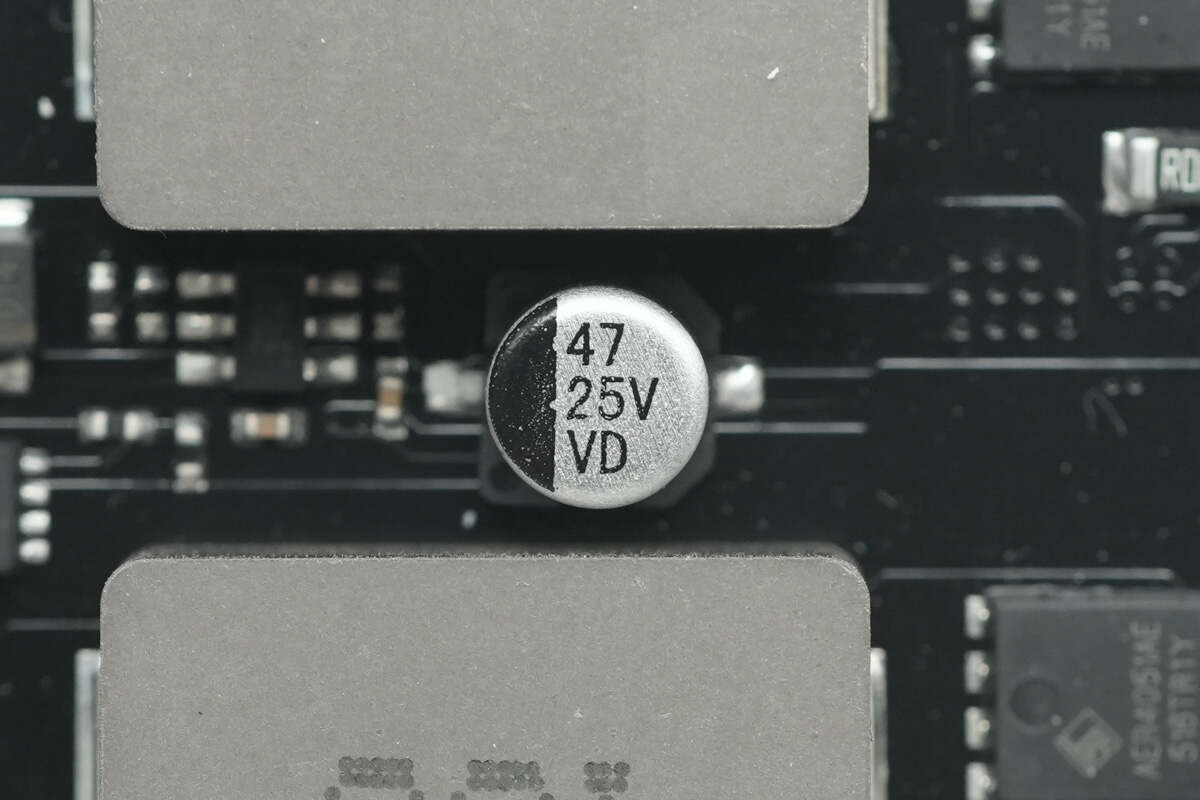
The filter capacitor is rated at 25V 47μF.
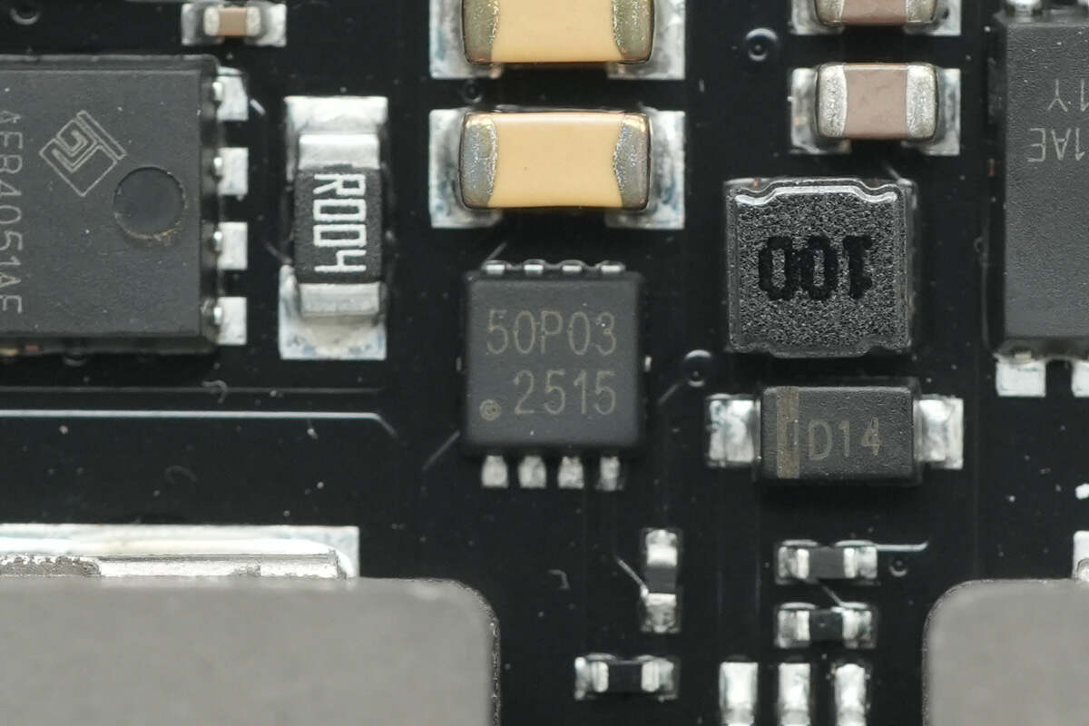
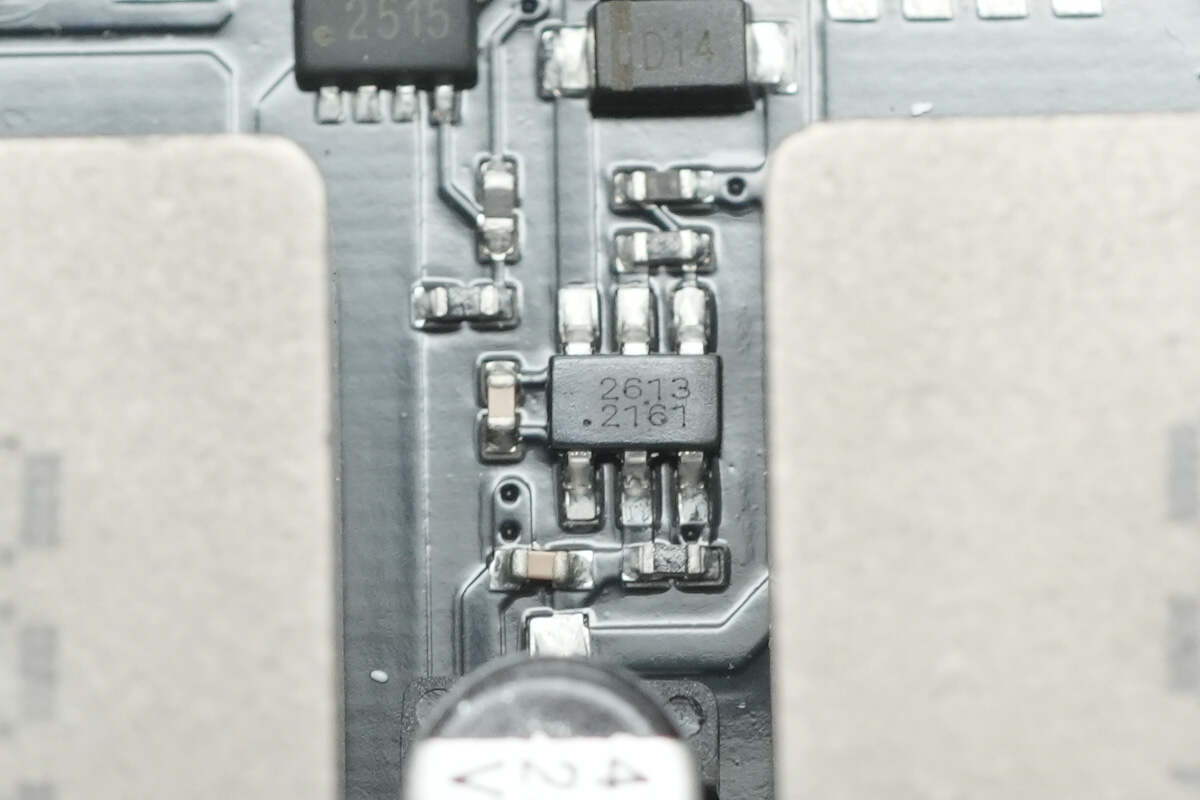
Here’s a close-up of the MOSFET marked with 50P03.
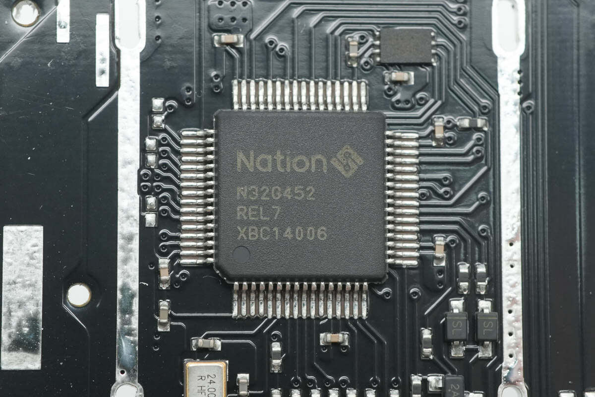
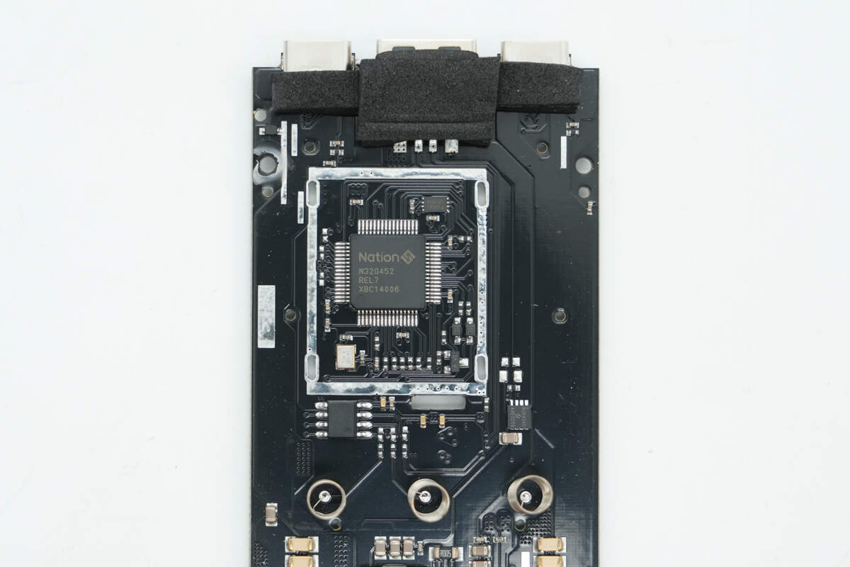
The MCU used for overall system control is from Nations, model N32G452REL7. This series features a 32-bit ARM Cortex-M4F core with a maximum operating frequency of 144 MHz, supporting floating-point operations and DSP instructions. It comes in an LQFP64 package.
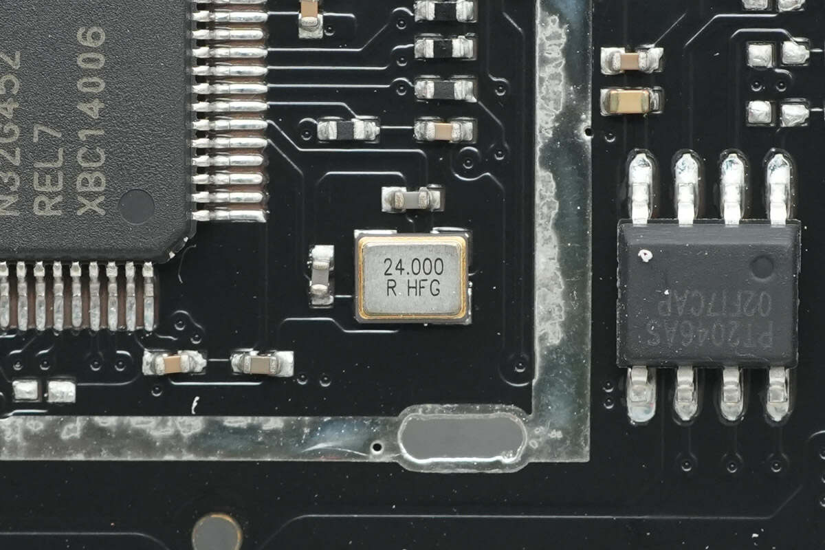
Here’s a close-up of the external 24,000 MHz clock crystal oscillator for the MCU.
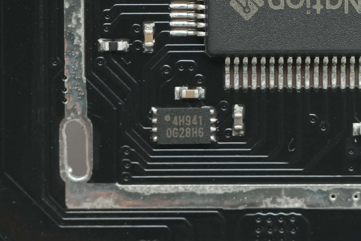
The memory chip for storing configuration data is from Winbond, marked 4H, model W25X40CL. It’s a serial NOR flash memory operating on a 2.3–3.6V single power supply, with a standby current as low as 1µA, and comes in a compact package.
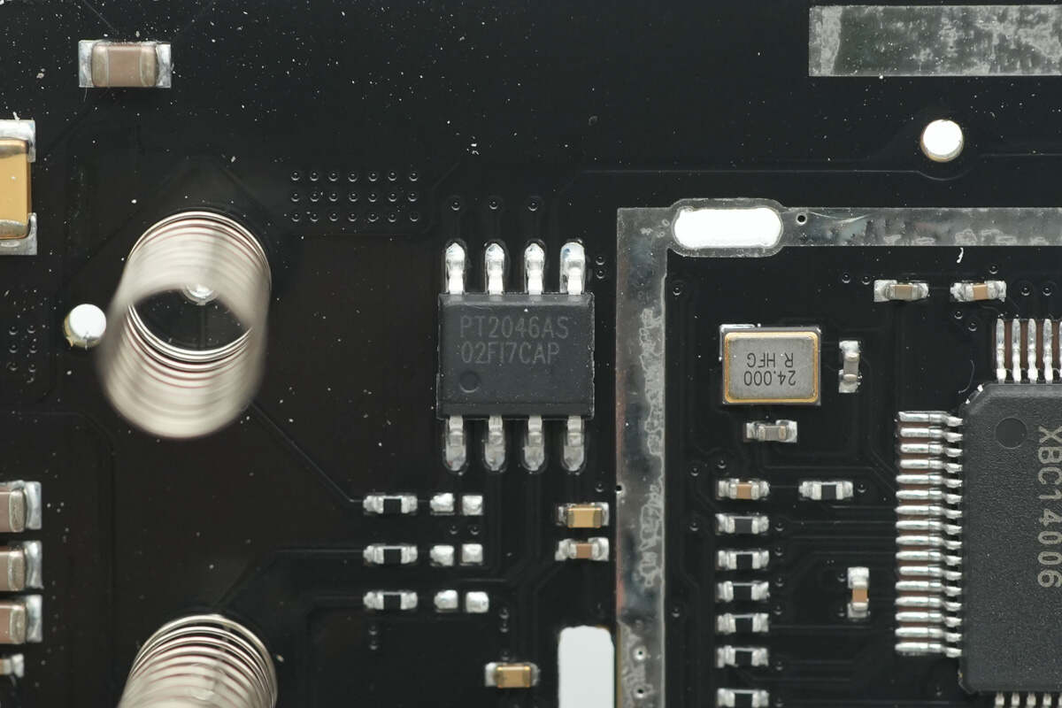
The touch chip is from PinTeng, model PT2046AS. It is a 3-key touch detection chip with a built-in voltage regulator that provides stable power to the touch sensing circuit. It also integrates an efficient and reliable touch detection algorithm for stable performance, and comes in an SOP8 package.
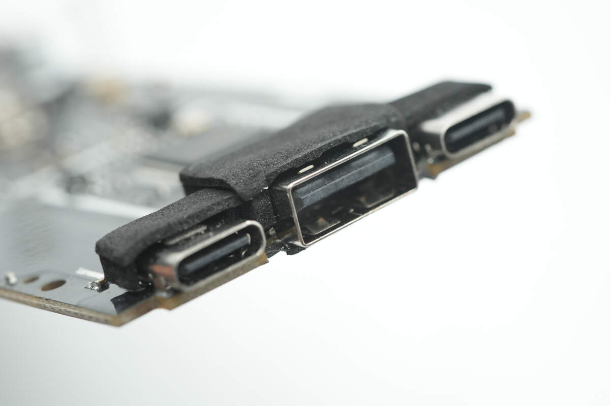
The USB sockets are covered with cushioning foam.
Well, those are all components of the Lenovo thinkplus FLUXO 140W 20000mAh Power Bank.
Summary of ChargerLAB
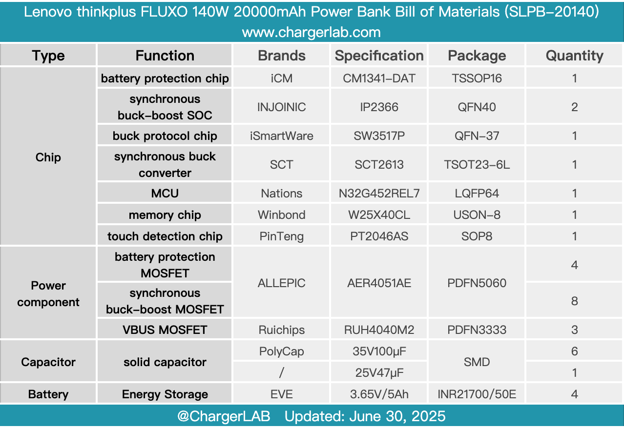
Here is the component list of the Lenovo thinkplus FLUXO 140W 20000mAh Power Bank for your convenience.
Its design is highly futuristic and tech-inspired. The ergonomic 39 mm thickness and 4.5 mm biomimetic rounded corners provide a comfortable grip. Equipped with a 2.01-inch TFT screen displaying battery capacity, power, temperature, and more, combined with a sports car dashboard style, it greatly enhances the user experience.
It features the industry’s first digital hybrid charging technology and supports hot-swapping of multiple ports without interruption, enabling dynamic power distribution. It offers multiple output configurations like 65W+65W, 100W+30W, and 65W+40W+30W to simultaneously fast-charge laptops, tablets, smartphones, and other devices.
It fully complies with the stringent GB 31241-2022 and GB 4943.1-2022 standards. The battery’s positive and negative materials, separator, electrolyte, and other safety components, as well as key manufacturing processes, have undergone rigorous testing—including repeated lithium dendrite formation cycles—to evaluate aging safety. Intelligent monitoring of battery voltage, temperature, and other safety parameters meets all requirements. This demonstrates Lenovo’s strong commitment to charging safety, always prioritizing the personal and property safety of its users.
After taking it apart, we found that it uses four EVE INR21700/50E automotive-grade battery cells, designed and tested to standards far exceeding ordinary cells, and certified with CCC. It is also equipped with the iCM CM1341-DAT lithium battery protection system, along with a thermistor for temperature monitoring and real-time feedback.
Both USB-C ports utilize the Injoinic IP2366 bidirectional synchronous buck-boost power management solution to enable two-way fast charging. The USB-A port uses the iSmartWare SW3517P for buck output control. The entire system is managed by the Nations N32G452REL7 MCU, while PolyCap capacitors are used for filtering. Overall, the product features solid and reliable components and construction.
Related Articles:
1. Teardown of DJI 2600W 1024Wh Power 1000 V2 Portable Power Station
2. Teardown of HUAWEI 100W SuperCharge Car Charger (P0019)
3. Teardown of Nintendo Switch 2 Official Charging Dock