Introduction
We recently acquired the IM Motors 50W in-car wireless charging module. The unit integrates NFC functionality and features a PCB shielding plate, designed to be installed beneath the interior trim panel. It provides a single charging position and uses an aluminum alloy housing on the rear side. A cooling fan is incorporated, directing airflow from the bottom to dissipate heat from both the smartphone and the wireless charging module. Next, let’s take a closer look at its internal components and design.
Product Appearance
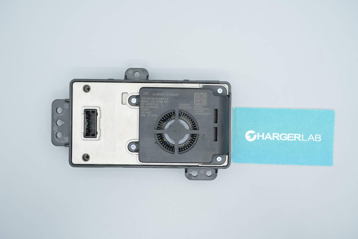
The aluminum alloy back cover is secured with screws.
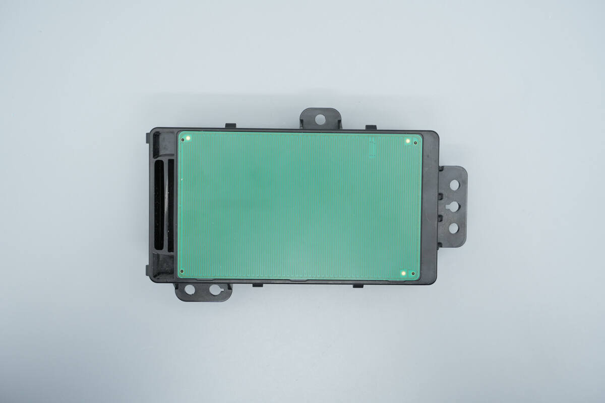
The front side features a PCB shielding panel, with an air outlet positioned on the left.
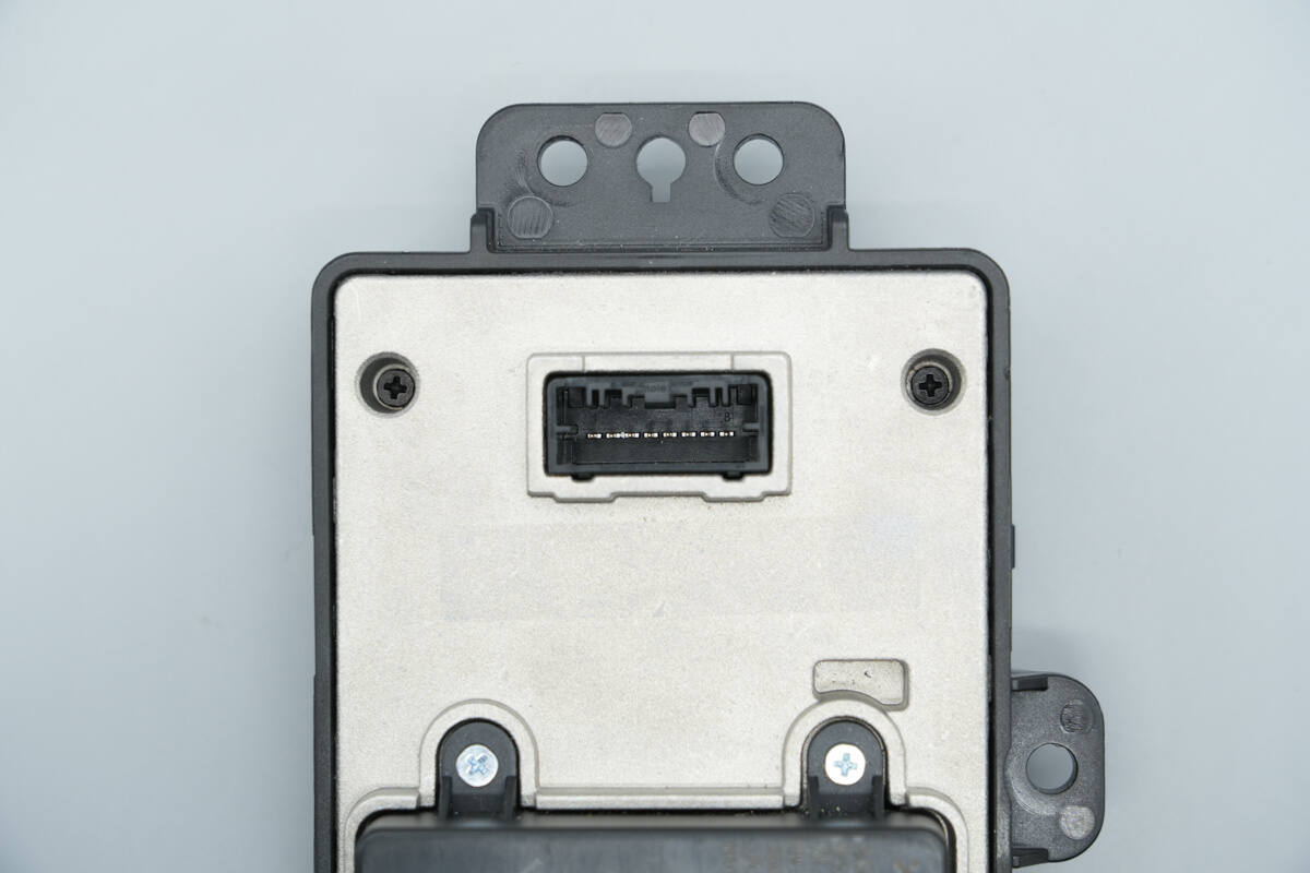
The power connector terminals are located at the top of the back cover.
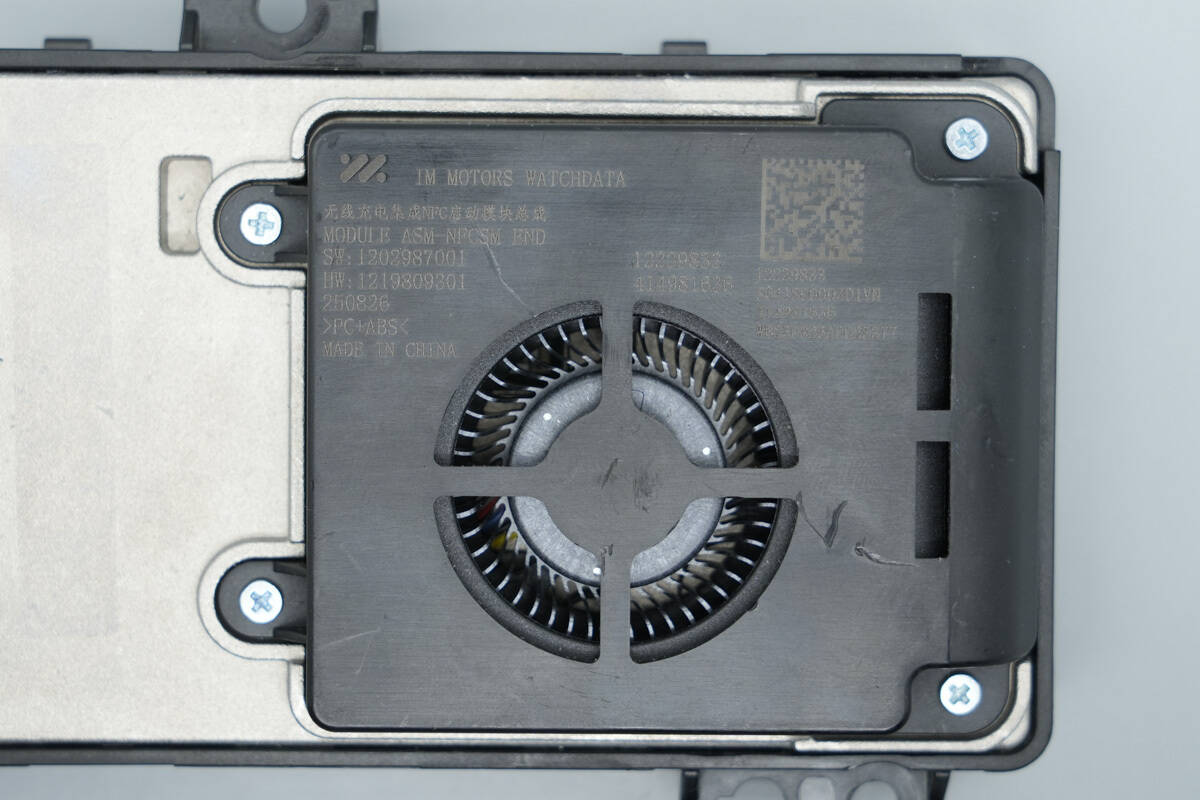
The fan cover is printed with product information:
Wireless Charging Integrated NFC Activation Module Assembly
MODULE ASM NFCSM END
SW: 1208977001
HW: 1219809301
250826
PC+ABS<
Made in China
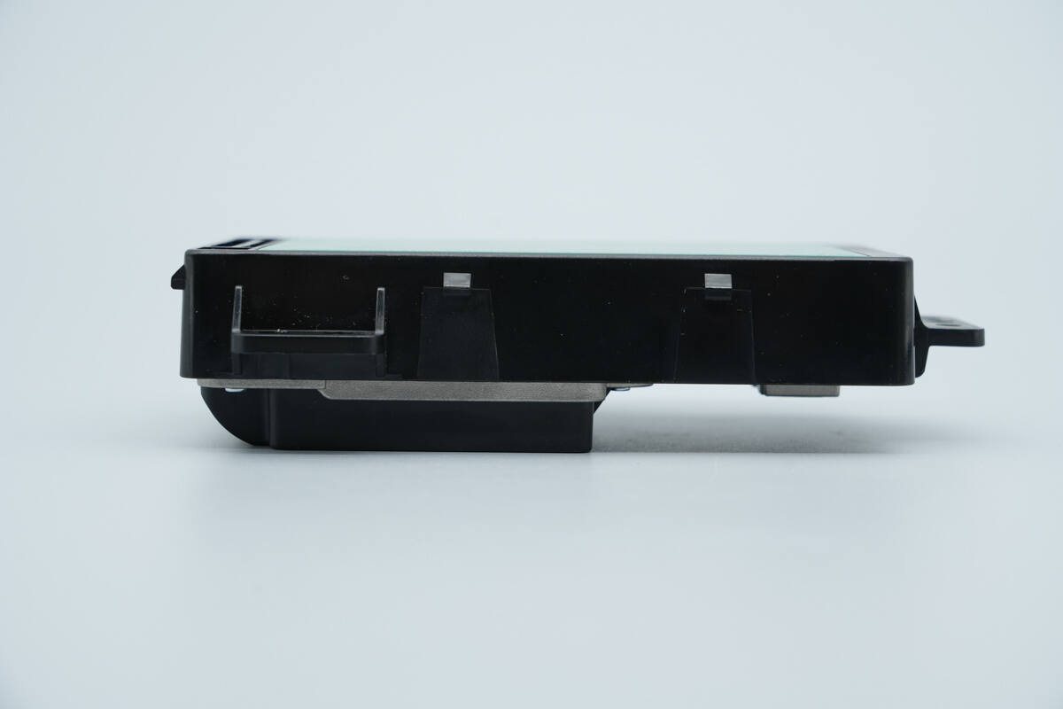
From the side view, the protrusion of the cooling fan is visible.
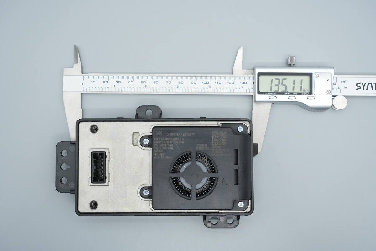
The length of the module is about 135.1 mm (5.32 inches).
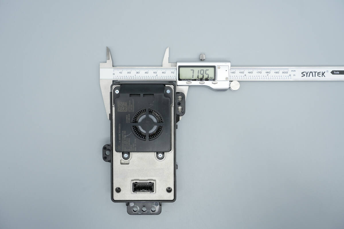
The width is about 72 mm (2.83 inches).
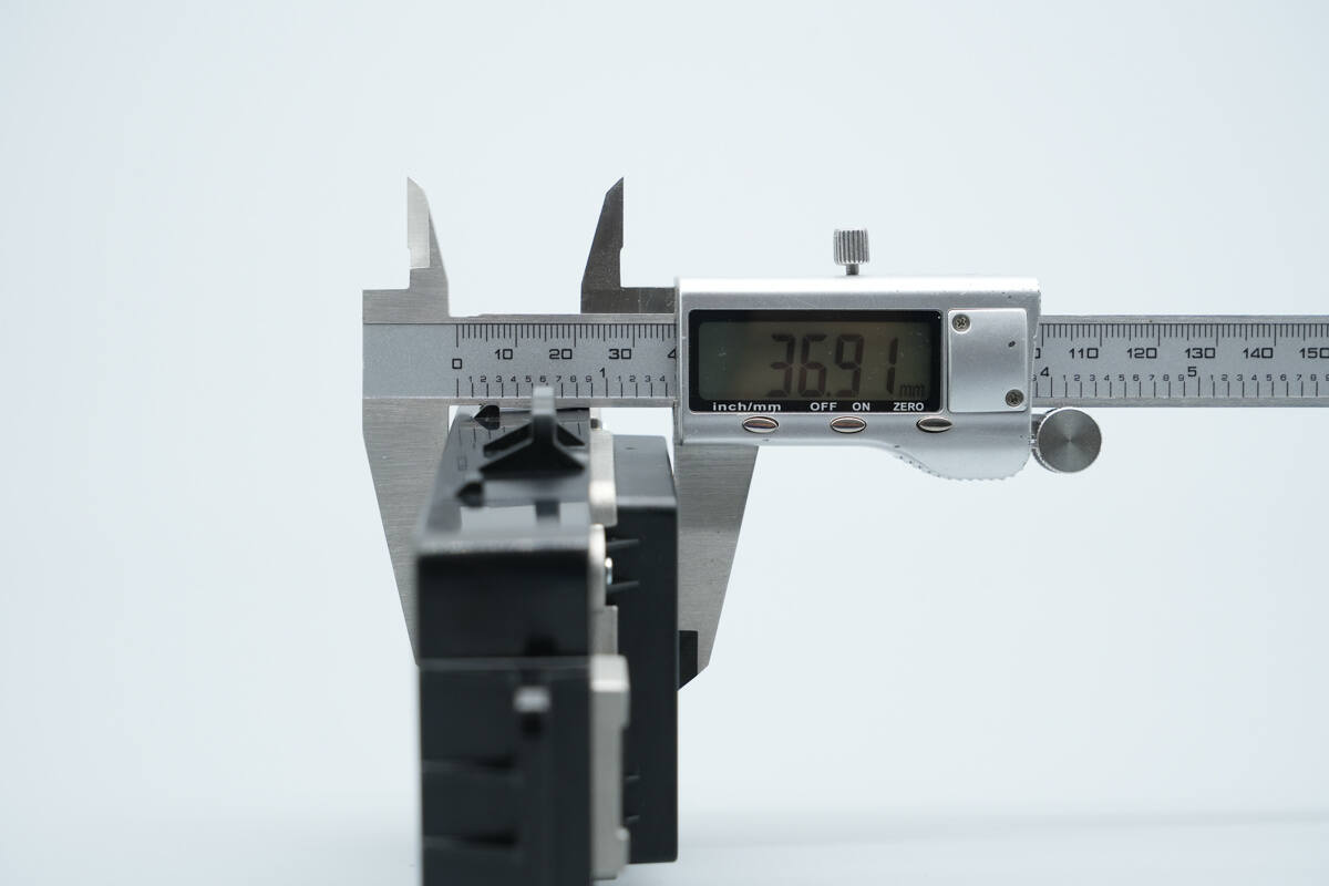
The thickness is about 36.9 mm (1.45 inches).
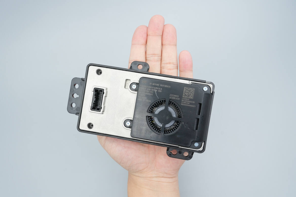
That's how big it is in the hand.
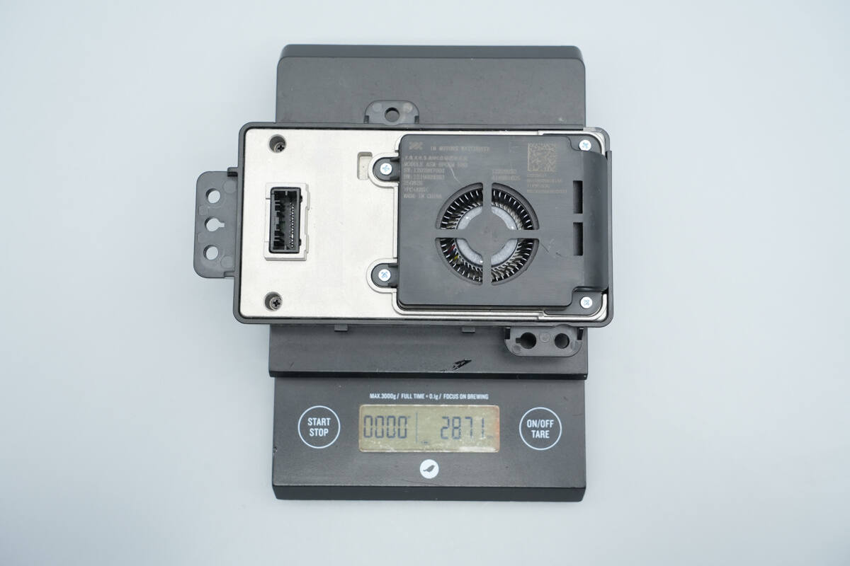
The weight is about 287 g (10.12 oz).
Teardown
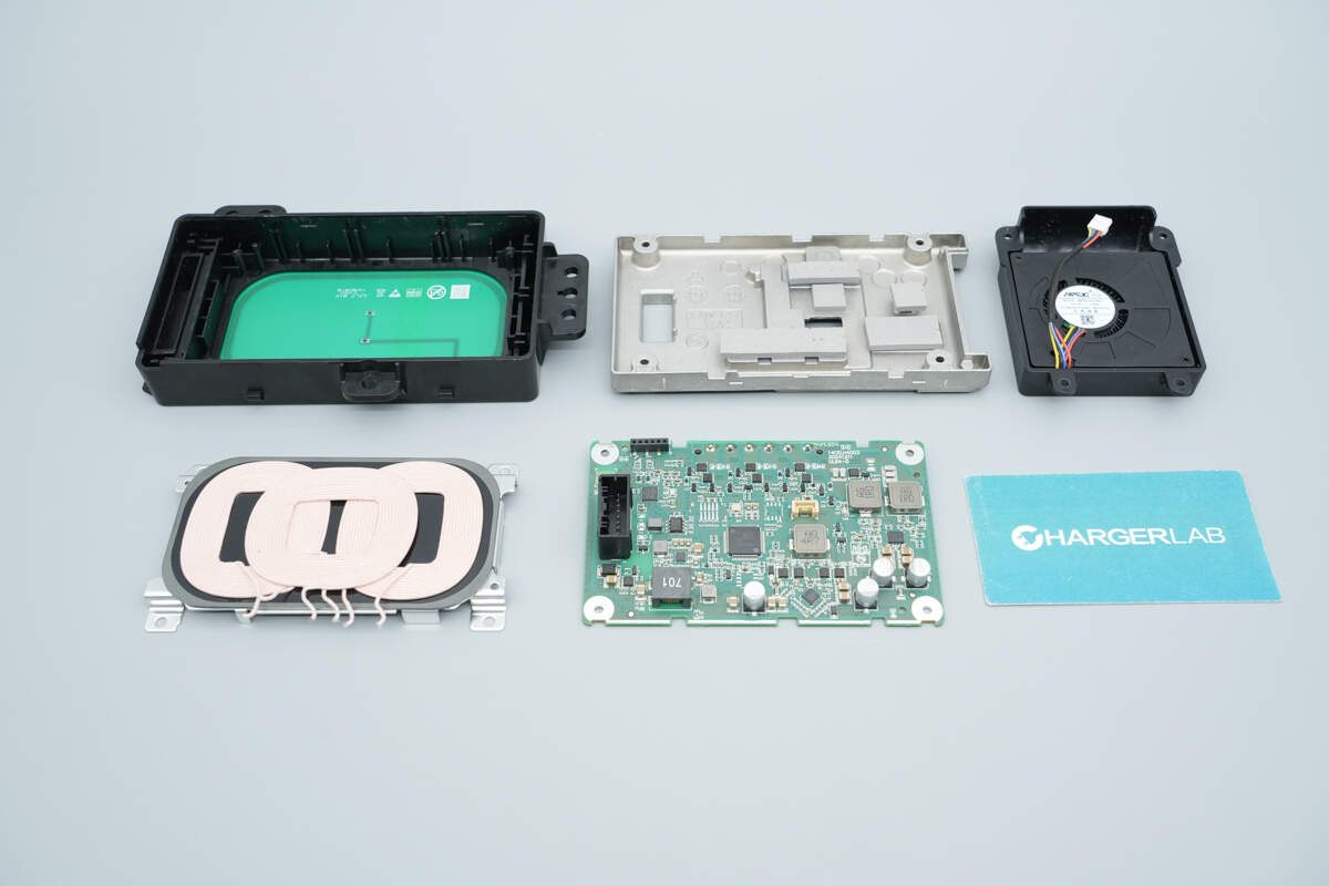
Next, let's take it apart to see its internal components and structure.
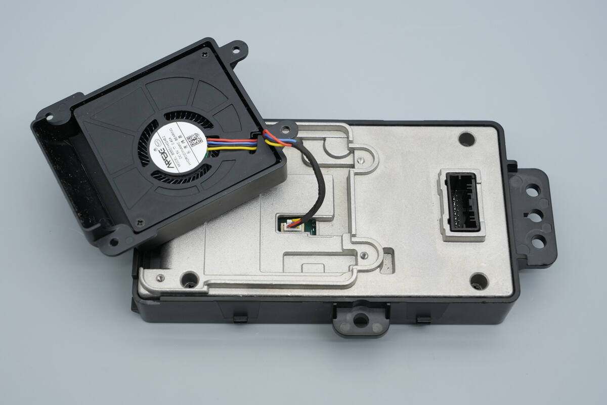
Unscrew the screws to remove the cooling fan.
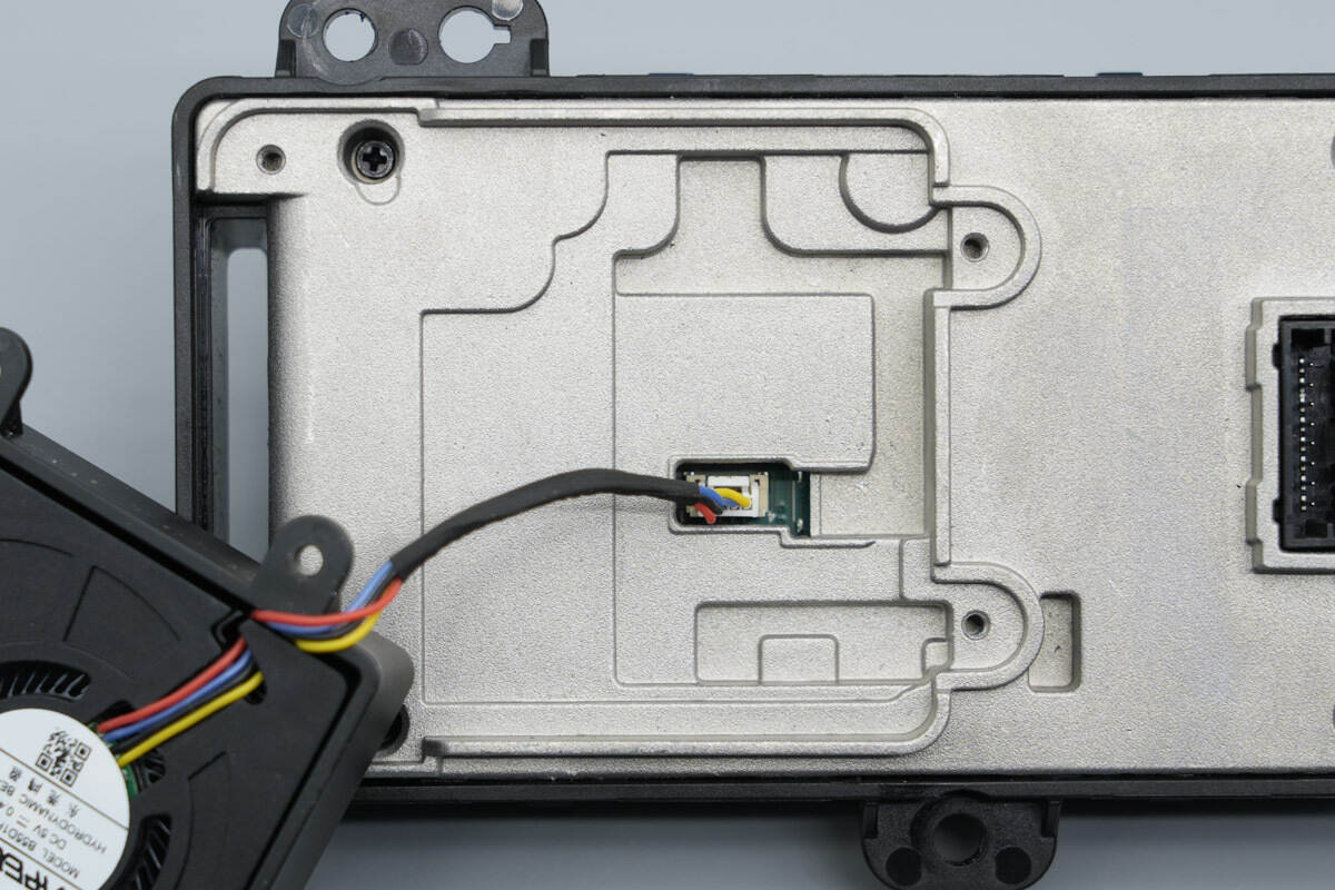
The fan is powered via a plug-in connector.
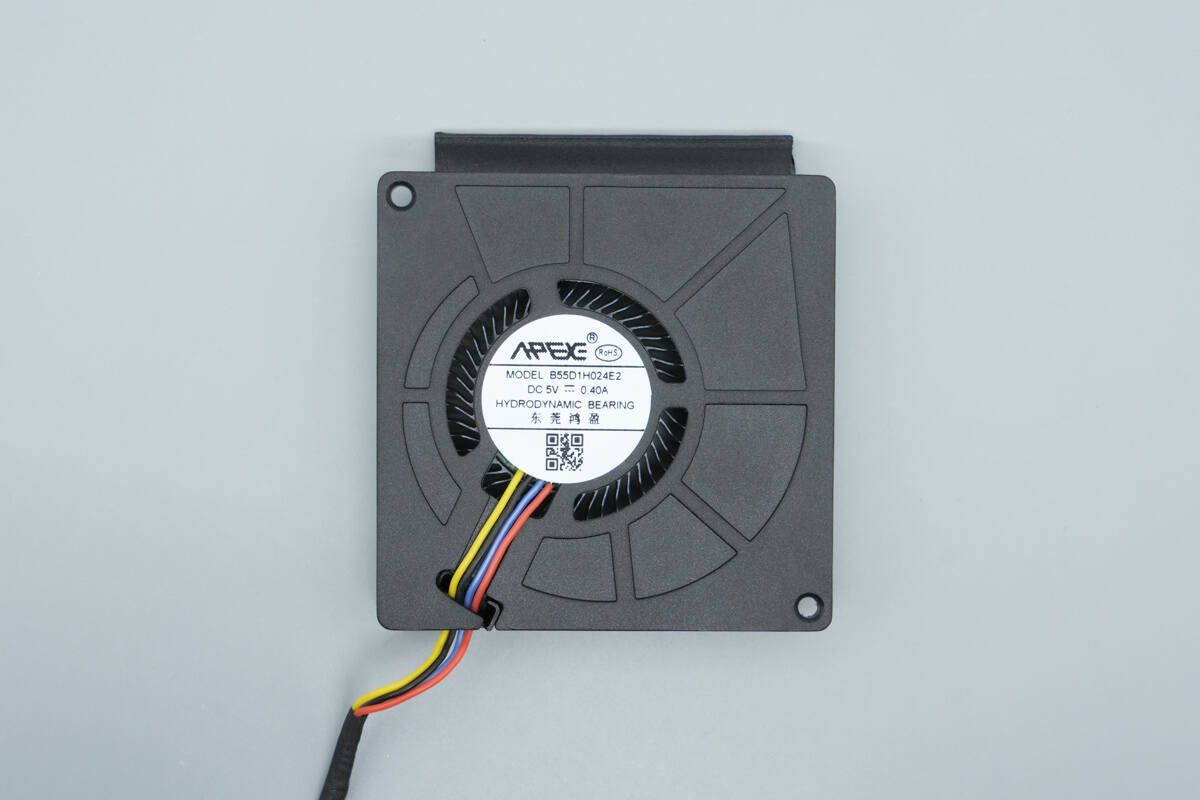
The cooling fan is from Hongying, model B55D1H024E2, with specifications of 5V 0.4A.
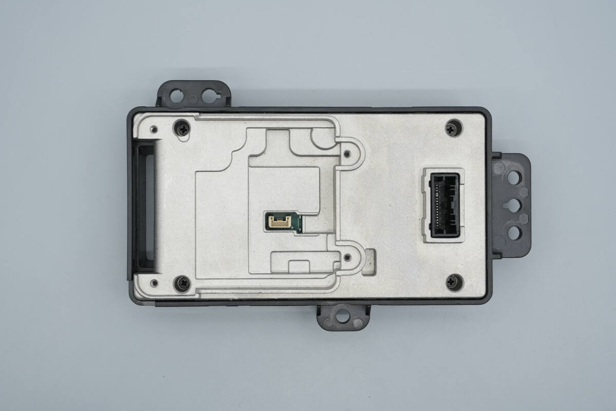
The aluminum alloy back cover is secured with screws.
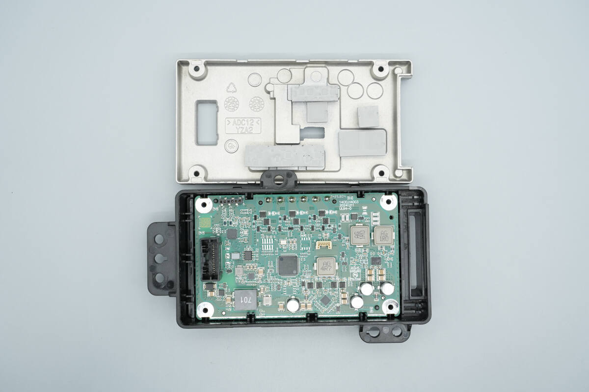
The interior of the back cover houses the PCBA module.
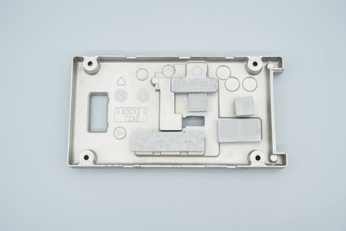
Thermal pads are placed on the back cover corresponding to the positions of the inductors and heat-generating components.
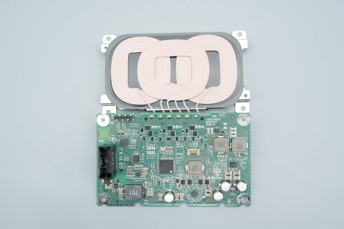
Remove the PCBA module along with the wireless charging coils.
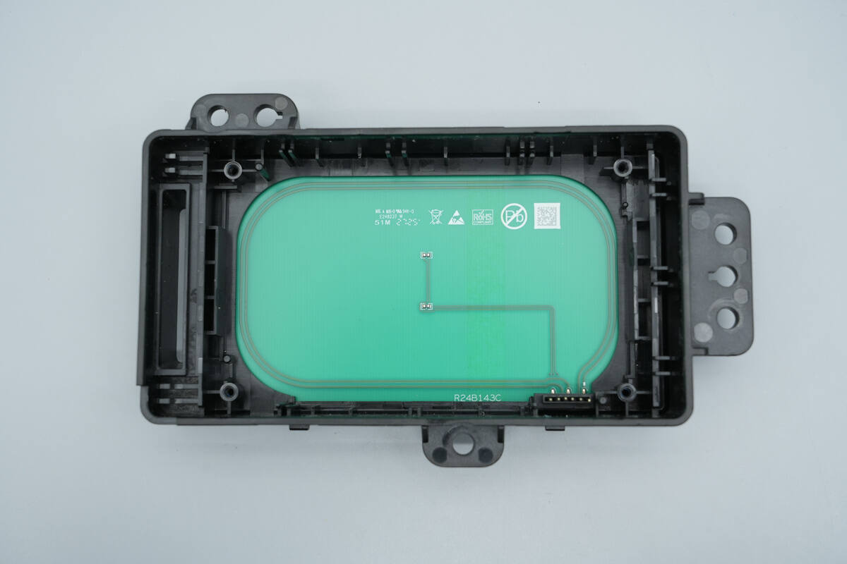
The lower layer of the PCB contains the NFC coil and a thermistor.

This is the connector socket linked to the PCBA module.
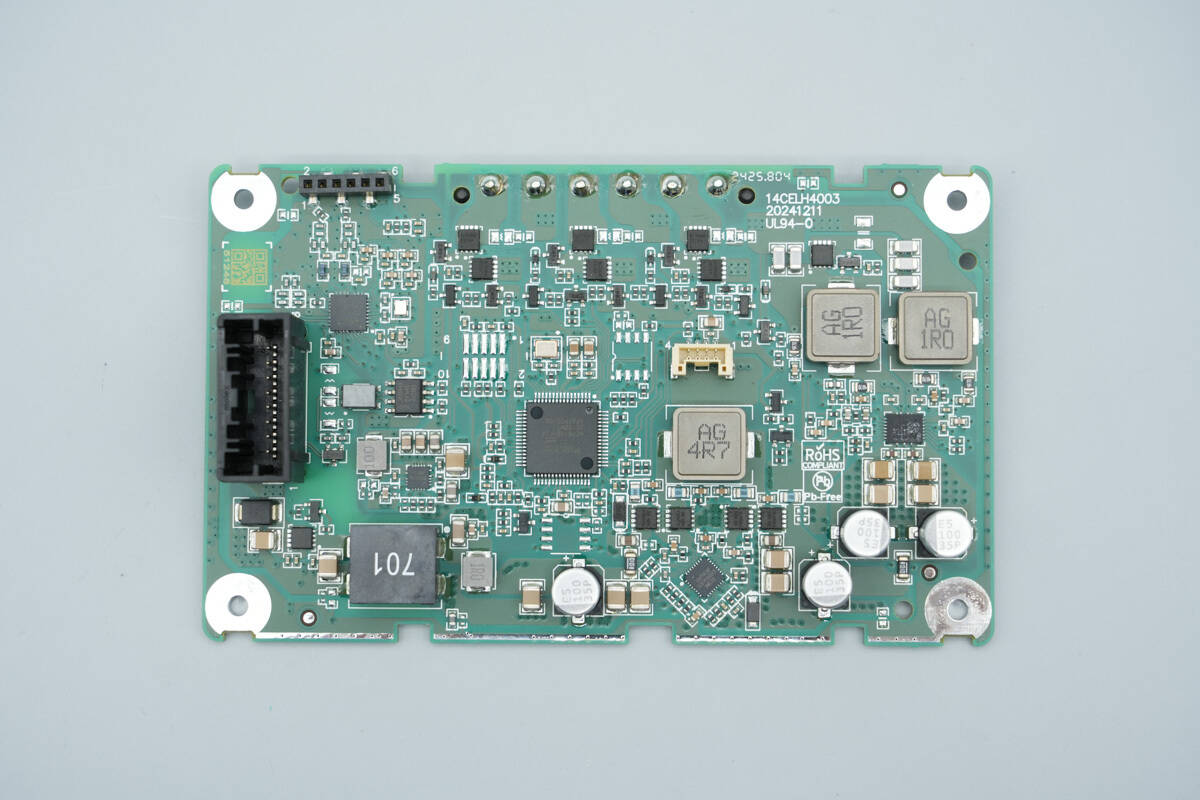
The front side of the PCBA module features a power connector, NFC reader chip, TVS diode, power control MOSFET, filter inductors, wireless charging master controller, synchronous buck-boost controller, synchronous buck-boost MOSFETs, wireless charging power stage chip, and filter capacitors.
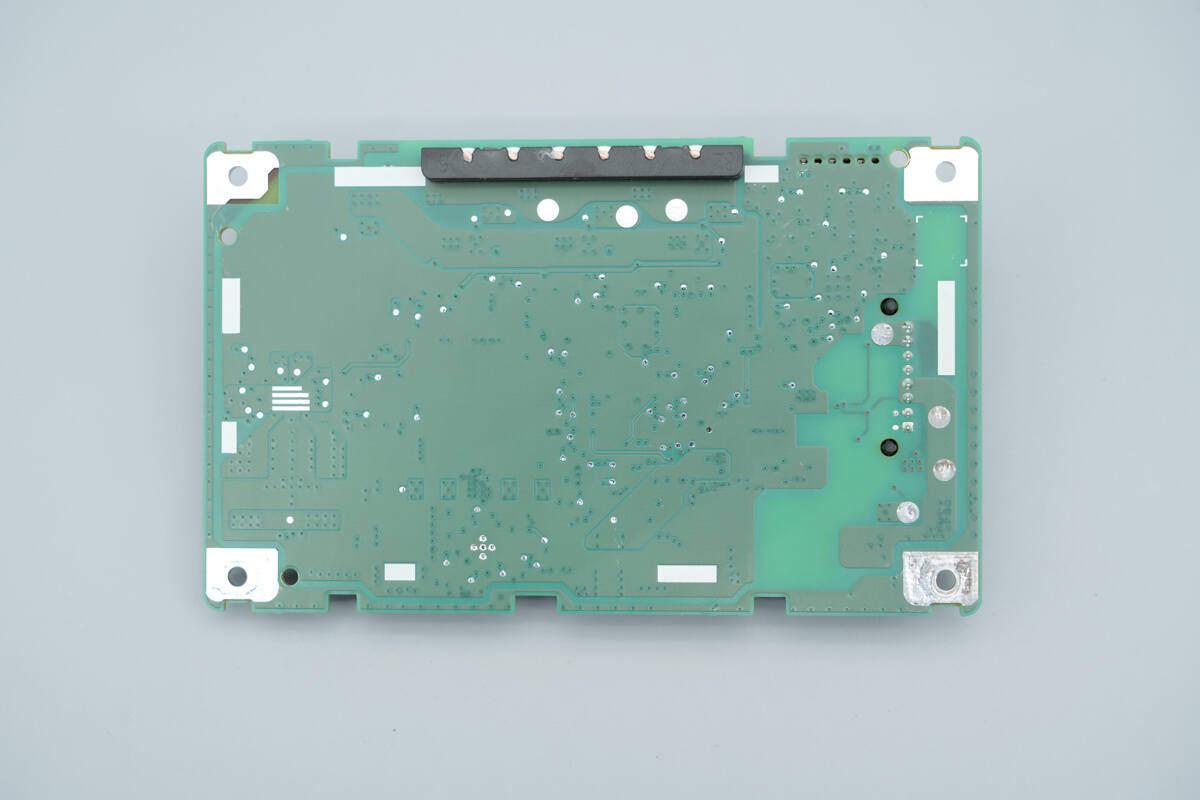
The back side has no components.
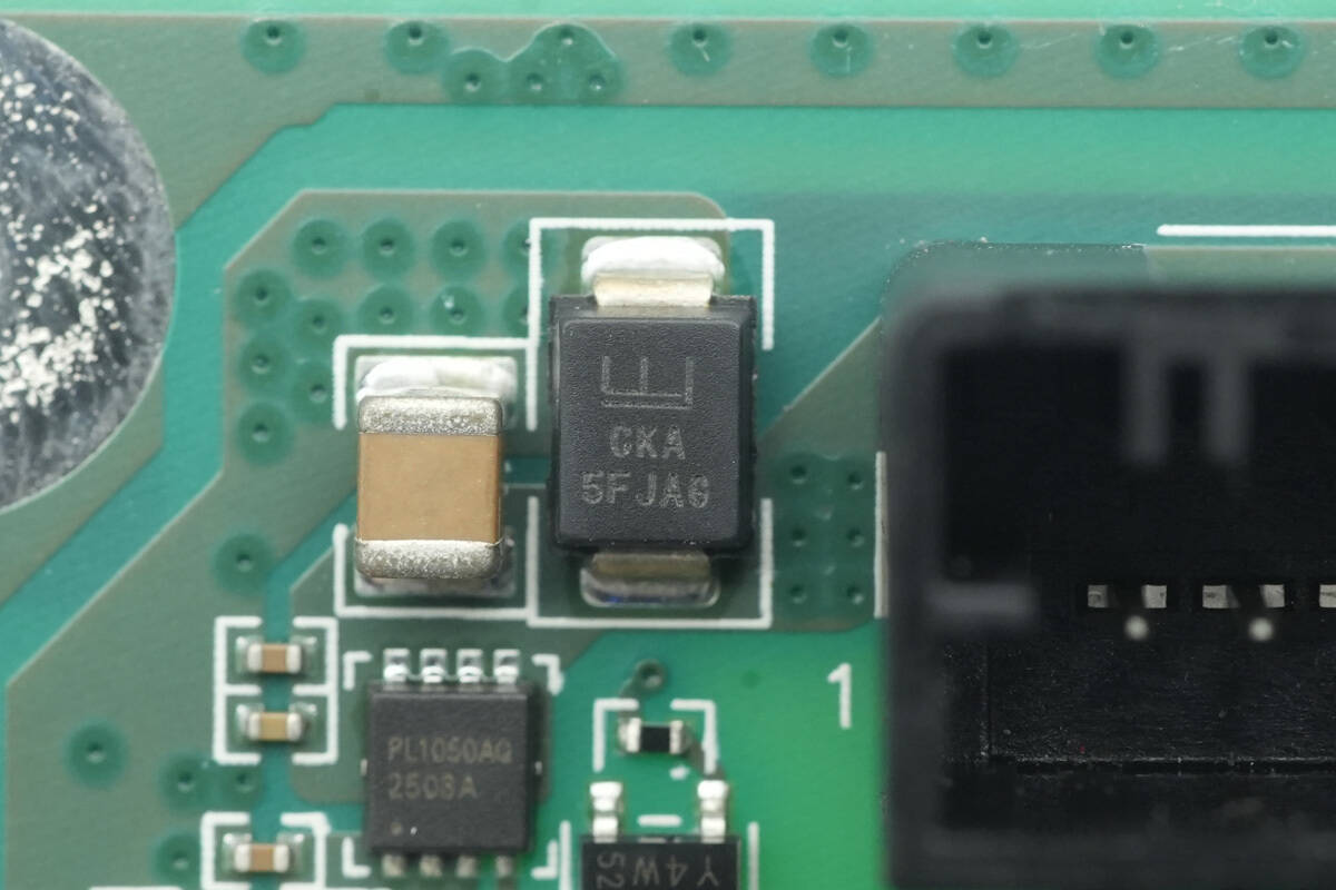
The input-side TVS is from Littelfuse, marked CKA, model TPSMB30CA-VR. It is a bidirectional TVS diode compliant with the AEC-Q101 standard, featuring a reverse standoff voltage of 30V and packaged in DO-214AA.
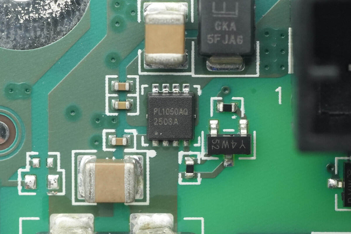
The power control switch transistor is from JJM, model JMPL1050AUQ. It is a PMOS device compliant with the AEC-Q101 standard, with a voltage rating of –100 V, an on-resistance of 38 mΩ, and comes in a PDFN3×3-8L package.
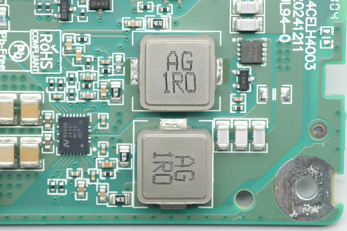
Close-up of the SMD common mode choke.
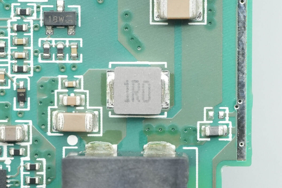
The 1 μH alloy inductor is used for input filtering.
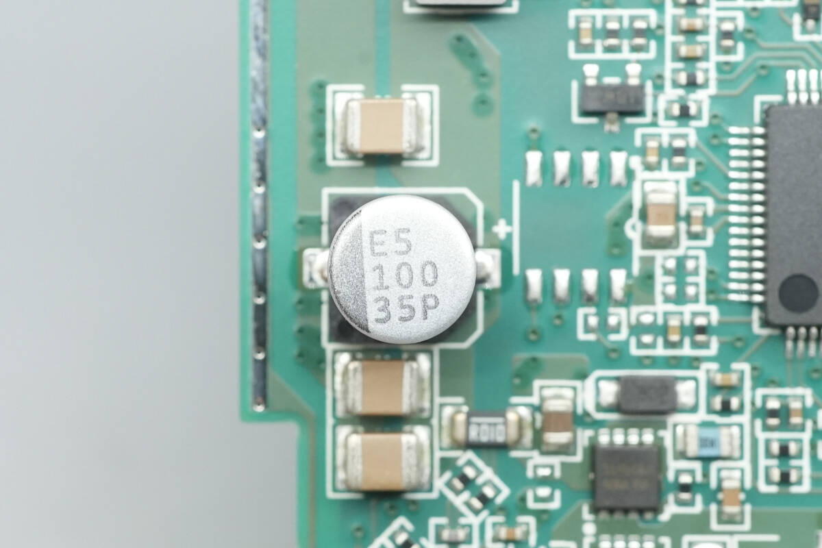
This filter capacitor has a specification of 100 μF, 35 V.
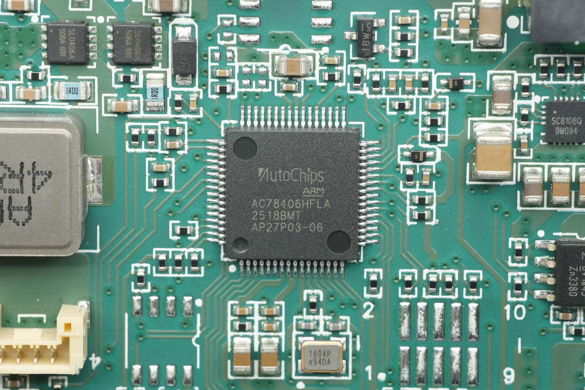
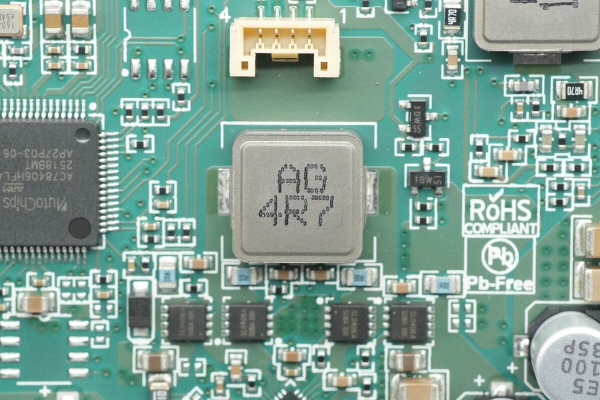
The MCU is from AutoChips, model AC78406HFLA. It is an automotive-grade MCU compliant with the AEC-Q100 Grade 1 standard, featuring an ARM Cortex-M4F core with a maximum frequency of 120 MHz and an integrated DSP. It includes 512 KB of flash memory, a CAN-FD module, as well as UART, SPI, and I²C interfaces. The MCU supports an operating temperature range of –40 °C to 125 °C and comes in an LQFP64 package.
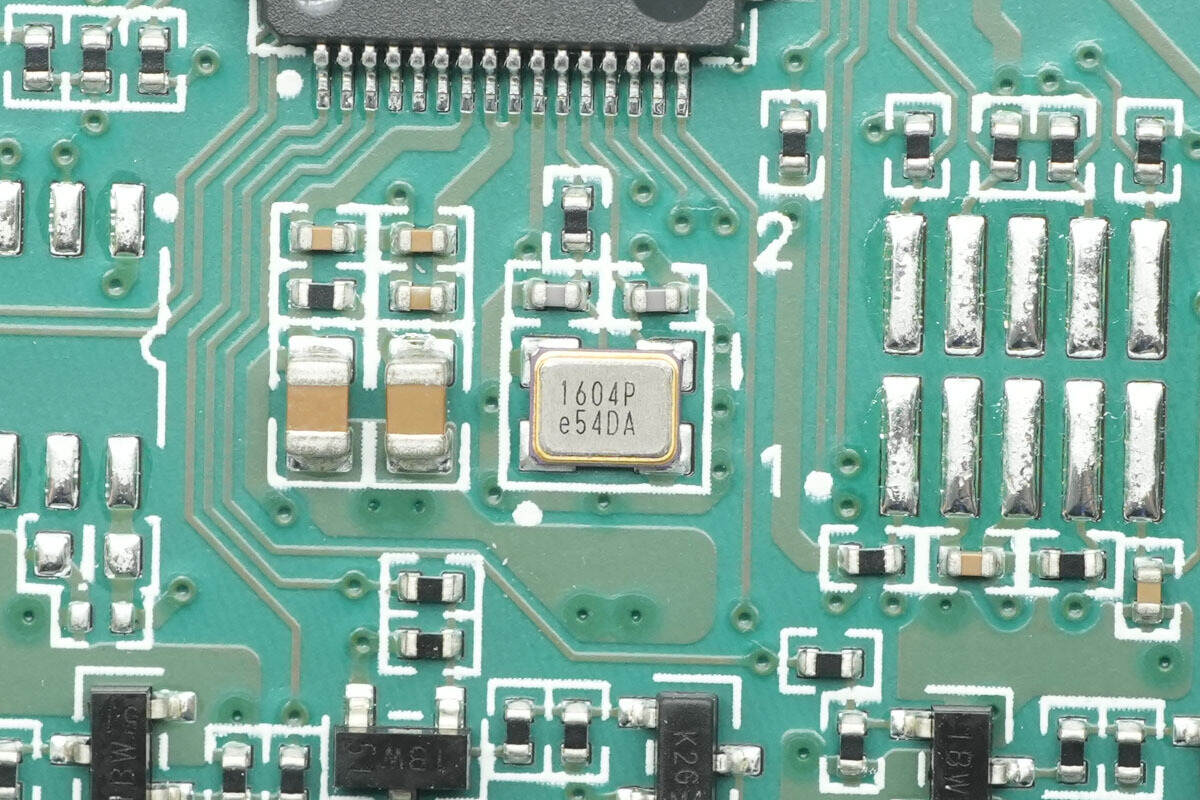
Close-up of the external clock crystal for the MCU.
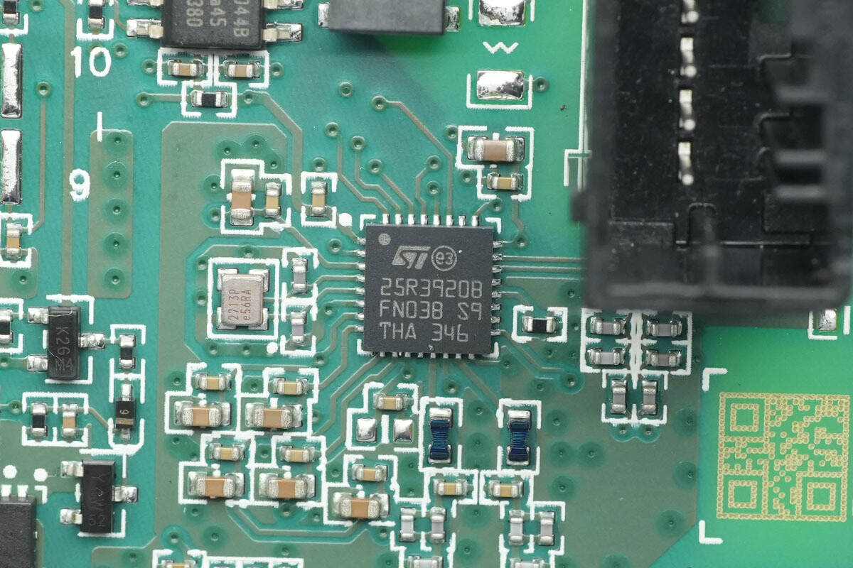
The NFC reader is from STMicro, model ST25R3920B. It is an automotive-grade device used for CCC digital keys and vehicle center consoles, compliant with the AEC-Q100 Grade 2 standard. It supports an operating voltage range of 2.6–5.5 V and a peripheral communication voltage range of 1.65–5.5 V, and comes in a VFQFPN32 package.
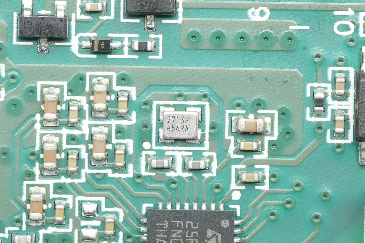
Close-up of the clock crystal.
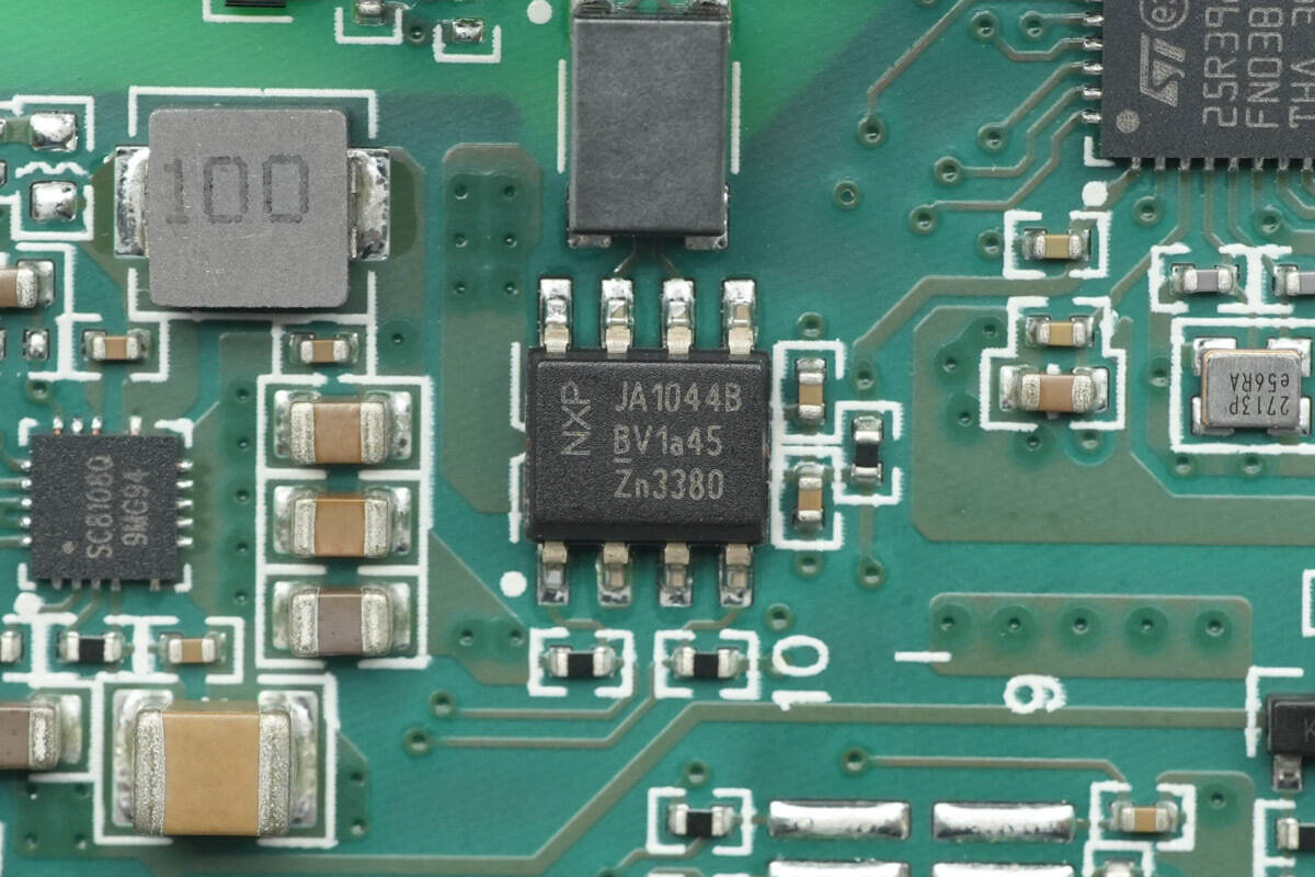
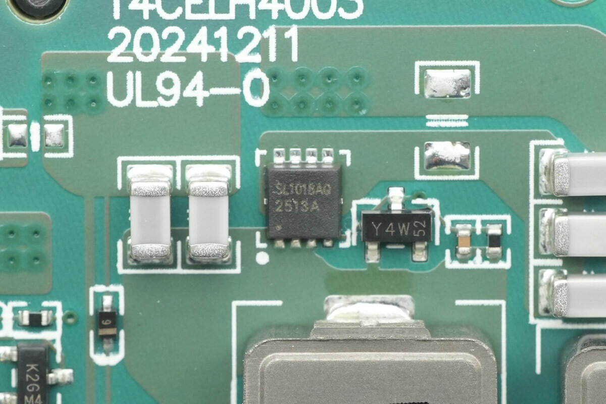
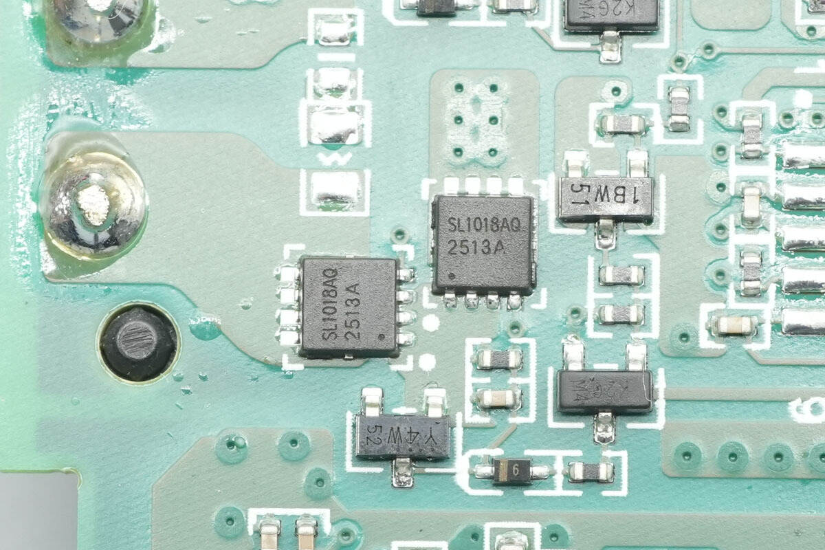
The CAN transceiver is from NXP, model TJA1044BT. It is a high-speed CAN bus transceiver supporting low-power mode and bus wake-up, and comes in an SO8 package.

Close-up of the SMD filter inductor for the CAN bus.
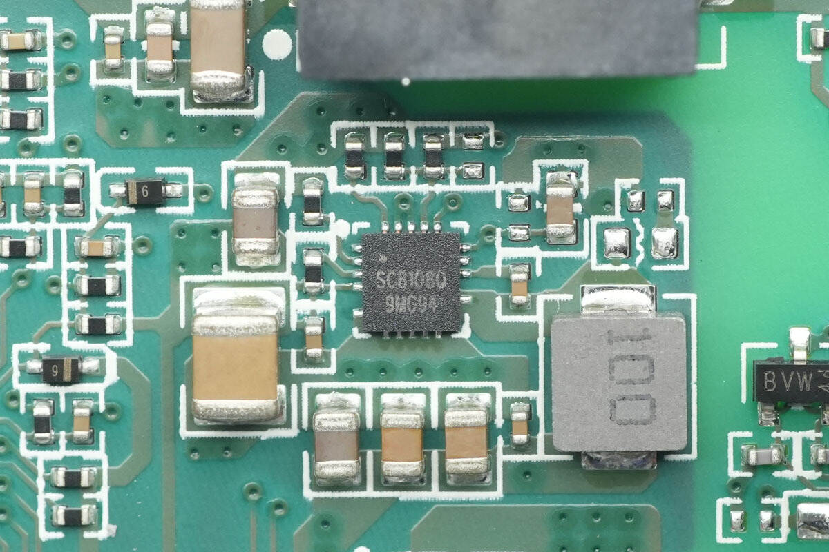
The synchronous buck chip is from SouthChip, model SC8108Q. It is automotive-grade, compliant with the AEC-Q100 Grade 1 standard, supporting an input voltage range of 4.4–32 V and an output current of 3.5 A. It integrates a 45 mΩ PMOS and a 30 mΩ NMOS, with support for driving an external NMOS. The chip features programmable line-loss compensation, a programmable switching frequency, and protections for undervoltage, overvoltage, short circuit, and overtemperature. It comes in a QFN-19 package.
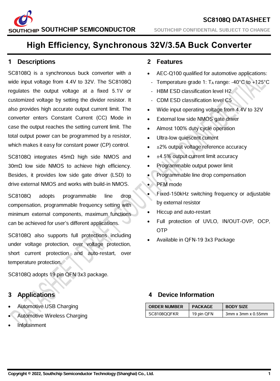
Here is the information about SouthChip SC8108Q.
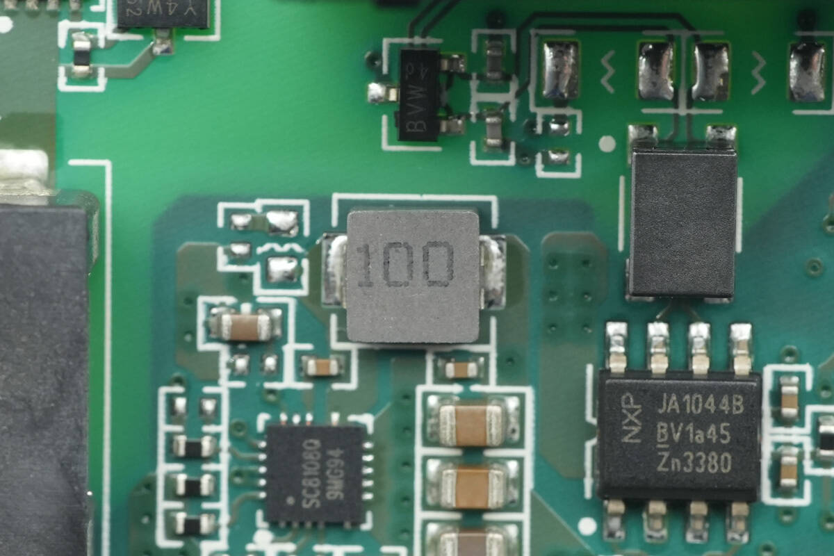
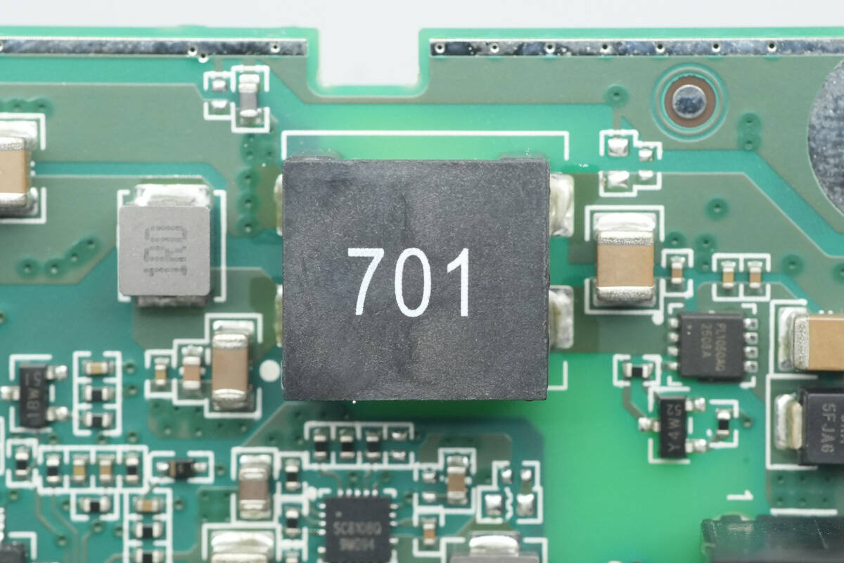
The 10 μH alloy inductor is used for the buck output.
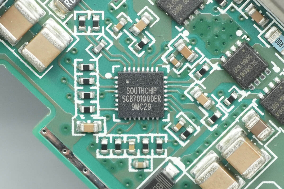
The synchronous buck-boost controller is from SouthChip, model SC8701Q. It is an automotive-grade device compliant with AEC-Q100 Grade 1, supporting an operating temperature range of –40 °C to 125 °C. This is a synchronous four-switch buck-boost controller capable of regulating the output voltage efficiently, whether it is higher, lower, or equal to the input voltage. It supports a wide input and output voltage range of 2.7–36 V and 2–36 V, respectively.
The driver voltage is set to 10 V to fully leverage external MOSFETs for maximum efficiency. The switching frequency is programmable from 200 to 600 kHz. The chip supports dynamic output voltage adjustment and current limiting, with input and output overcurrent protection, as well as overtemperature protection to ensure system safety. It comes in a QFN-32 package.
Here is the information about SouthChip SC8701Q.
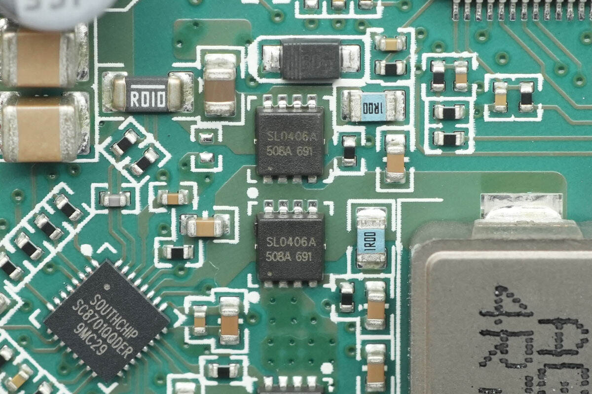
The synchronous buck-boost MOSFETs are from JJM, model JMSL0406AUQ. They are NMOS devices compliant with the AEC-Q101 standard, with a voltage rating of 40 V, an on-resistance of 4.5 mΩ, and come in a PDFN3×3-8L package.
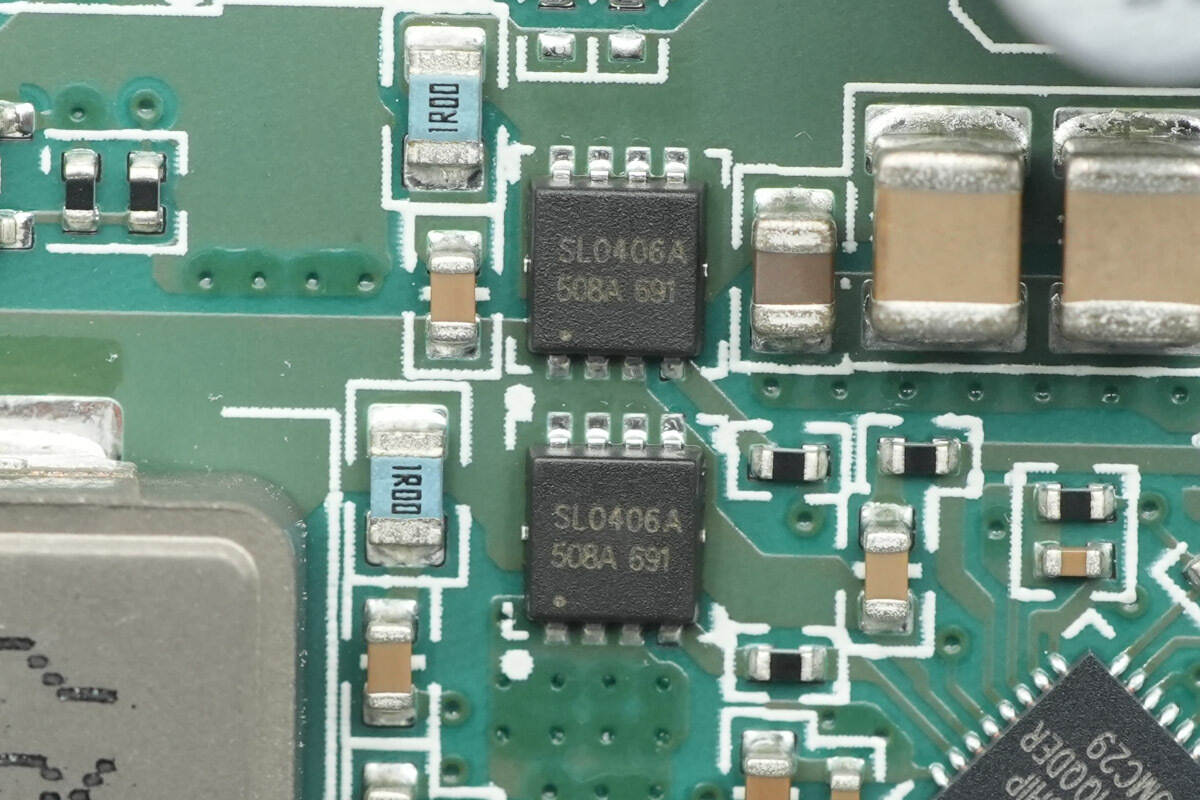
The other two MOSFETs are of the same model.
The 4.7 μH alloy inductor is used for the buck-boost conversion.
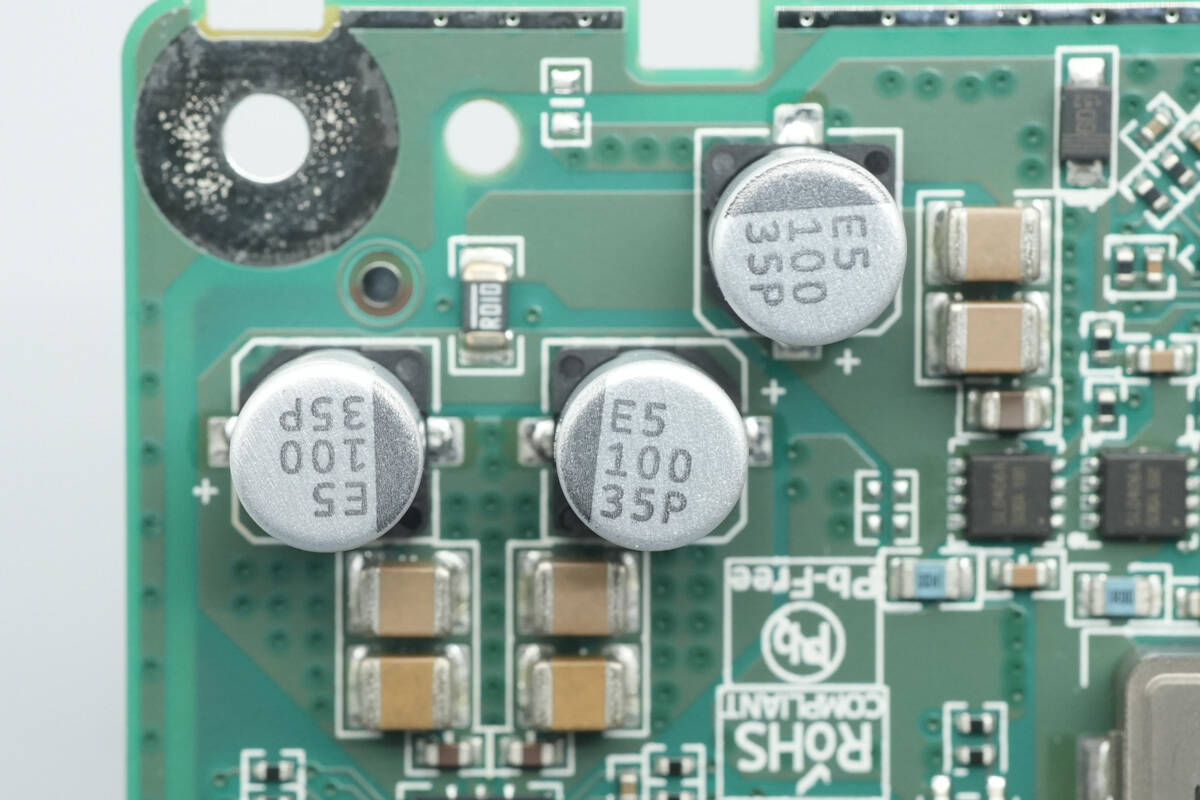
Three 100 μF, 35 V capacitors are used for output filtering.
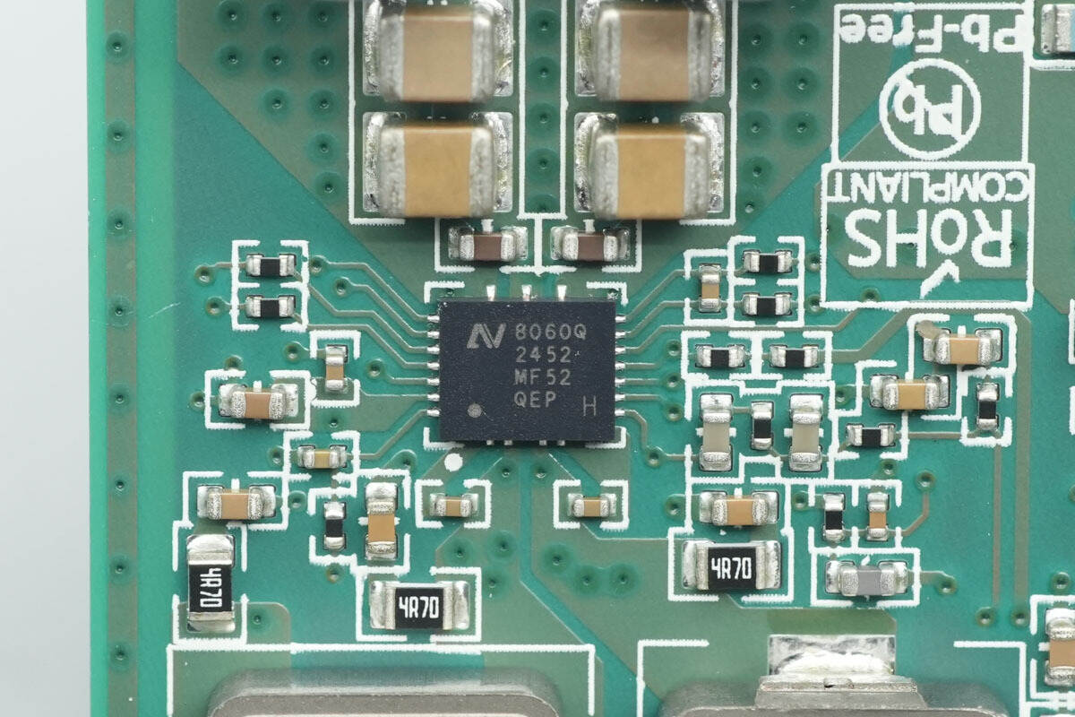
The wireless charging power stage chip is from NuVolta, model NU8060QH. It is a highly integrated, high-efficiency, and high-precision transmitter chip for wireless charging, compliant with the AEC-Q100 Grade 1 standard. The chip supports a wide input voltage range, with a recommended maximum operating voltage of 27 V and a transient voltage tolerance of up to 36 V. A single chip can drive wireless charging loads of up to 80 W, enabling high-power wireless fast charging.
The NU8060QH integrates a 12 mΩ low-resistance full bridge, offering superior thermal performance compared to existing products. It also incorporates many essential functions for wireless charging applications, including full-bridge driving, a 5 V LDO, high-precision current sensing, Q-factor detection, and built-in communication demodulation. The chip comes in a QFN21 package.
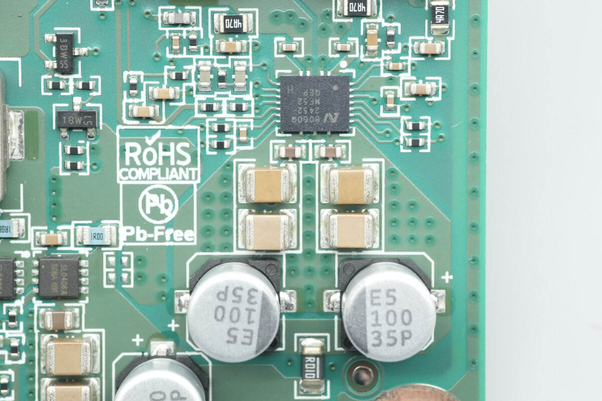
MLCCs are placed above the chip for filtering.
Two 1 μH alloy inductors are used for output filtering.
The MOSFET for the resonant capacitor is from JJM, model JMSL1018AUQ. It is an NMOS device compliant with the AEC-Q101 standard, with a voltage rating of 100 V, an on-resistance of 16.2 mΩ, and comes in a PDFN3×3-8L package.
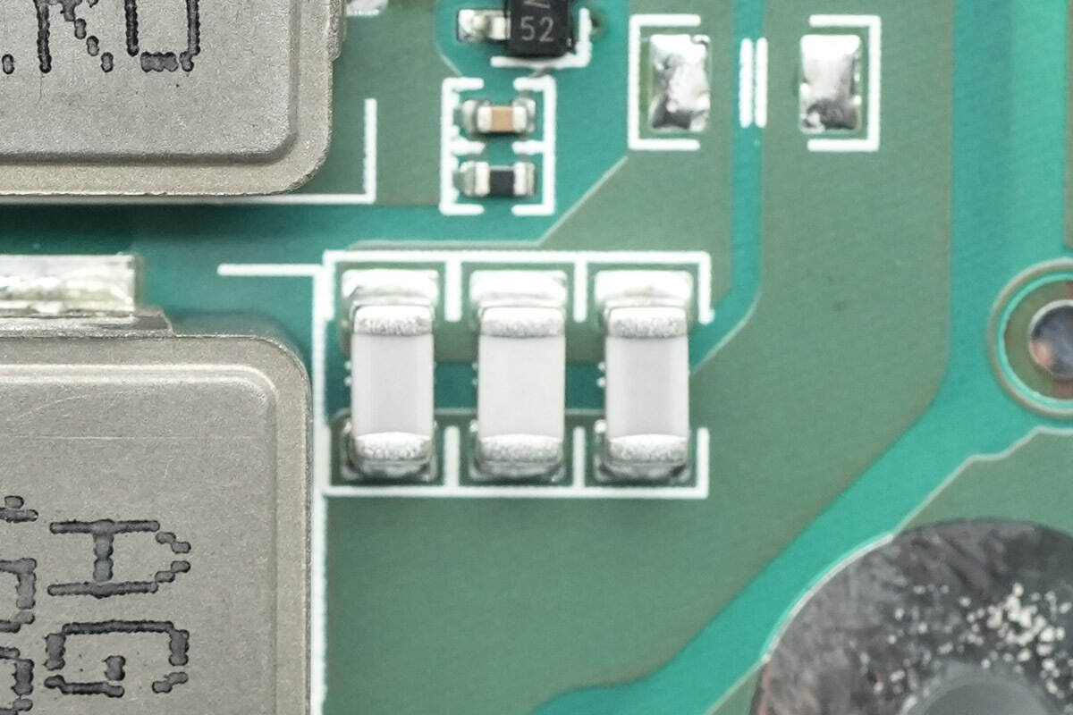
Close-up of the three parallel-connected resonant capacitors.
The coil switching MOSFETs are from JJM, model JMSL1018AUQ.
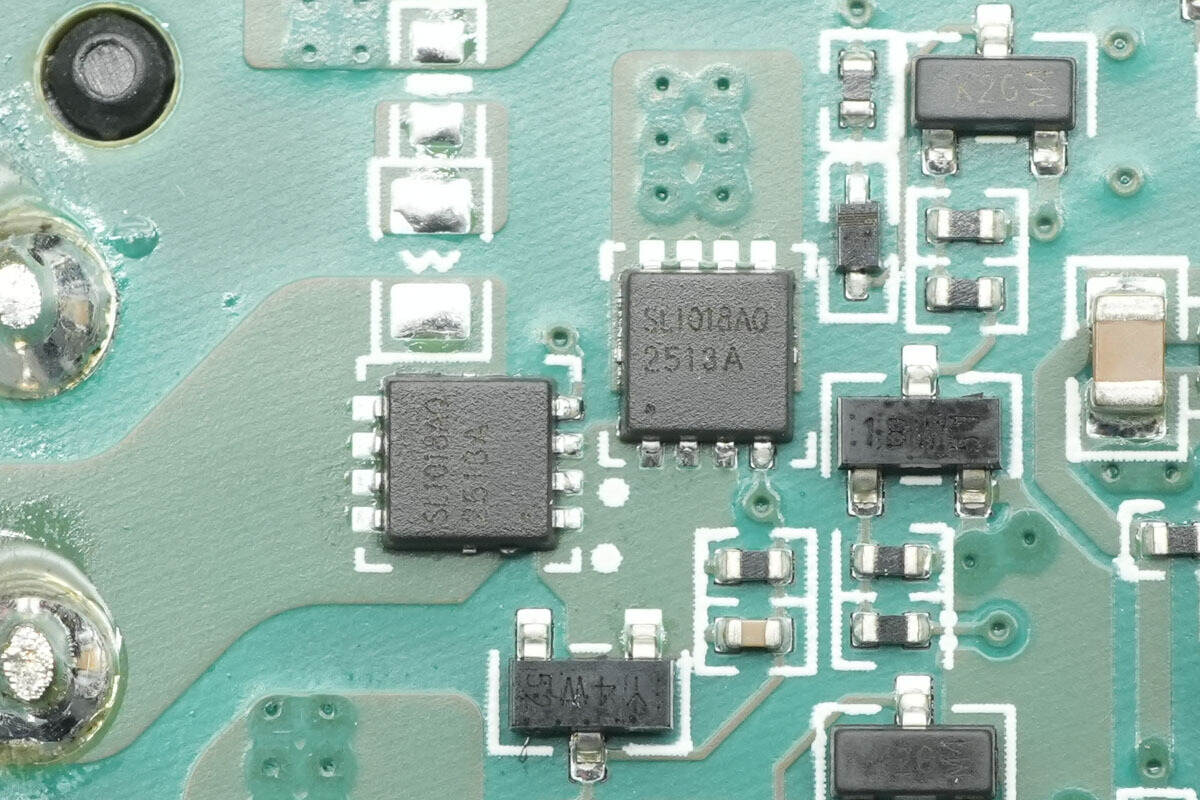
The other set of MOSFETs is of the same model.
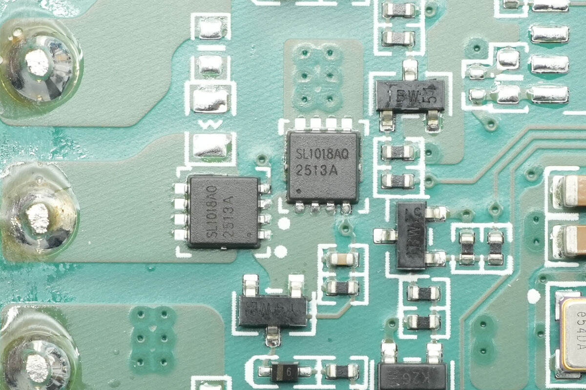
There are three sets in total, used for switching the three wireless charging coils.
Well, those are all components of the IM Motors 50W In-Car Pre-installed Wireless Charging Module.
Summary of ChargerLAB
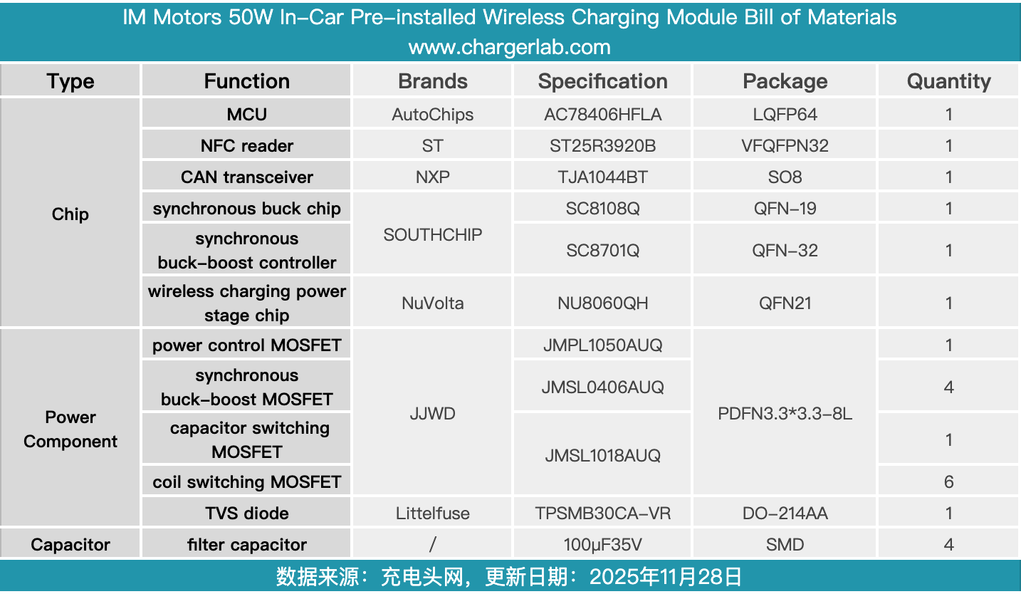
Here is the component list of the IM Motors 50W In-Car Pre-installed Wireless Charging Module for your convenience.
The module features a single charging position and supports 50W wireless charging. The rear side is equipped with an aluminum alloy back cover and a cooling fan, enhancing the wireless charging experience.
After taking it apart, we found that it uses the AutoChips AC78406HFLA as the wireless charging master controller, paired with the NuVolta NU8060QH for wireless power transmission. The SouthChip SC8701Q synchronous buck-boost controller handles the buck-boost voltage conversion to supply the wireless charging power stage chip, while the SC8108Q synchronous buck converter provides power to the wireless charging master controller.
The wireless charging module implements NFC functionality using the STMicro ST25R3920B and handles CAN bus communication via the NXP TJA1044BT. The input stage is protected against overvoltage by a Littelfuse bidirectional TVS diode. Power control, synchronous buck-boost conversion, and coil-switching MOSFETs are all sourced from JJM and are compliant with the AEC-Q101 standard. Thermal pads are applied inside the aluminum alloy cover to dissipate heat from inductors and chips. The module uses automotive-grade components, with neat workmanship and solid, reliable materials.
Related Articles:
1. Teardown of BYD 50W In-Car Pre-installed Wireless Charging Module
2. Teardown of CUKTECH 10 100W Car Charger with Retractable Cable (CC903P)
3. Teardown of Belkin BoostCharge Pro 100W 3-Port GaN Wall Charger (WCH016yz)