Introduction
HuntKey, a well-established manufacturer in the power supply sector, has been actively expanding in the GaN fast-charging market in recent years and has recently launched a 65W dual USB-C GaN fast charger. It features foldable plug pins, making it compact and portable. Both USB-C ports support 65W fast charging and are compatible with PD3.2 and PPS protocols. Below, we will take a closer look at the internal components and materials.
Product Appearance
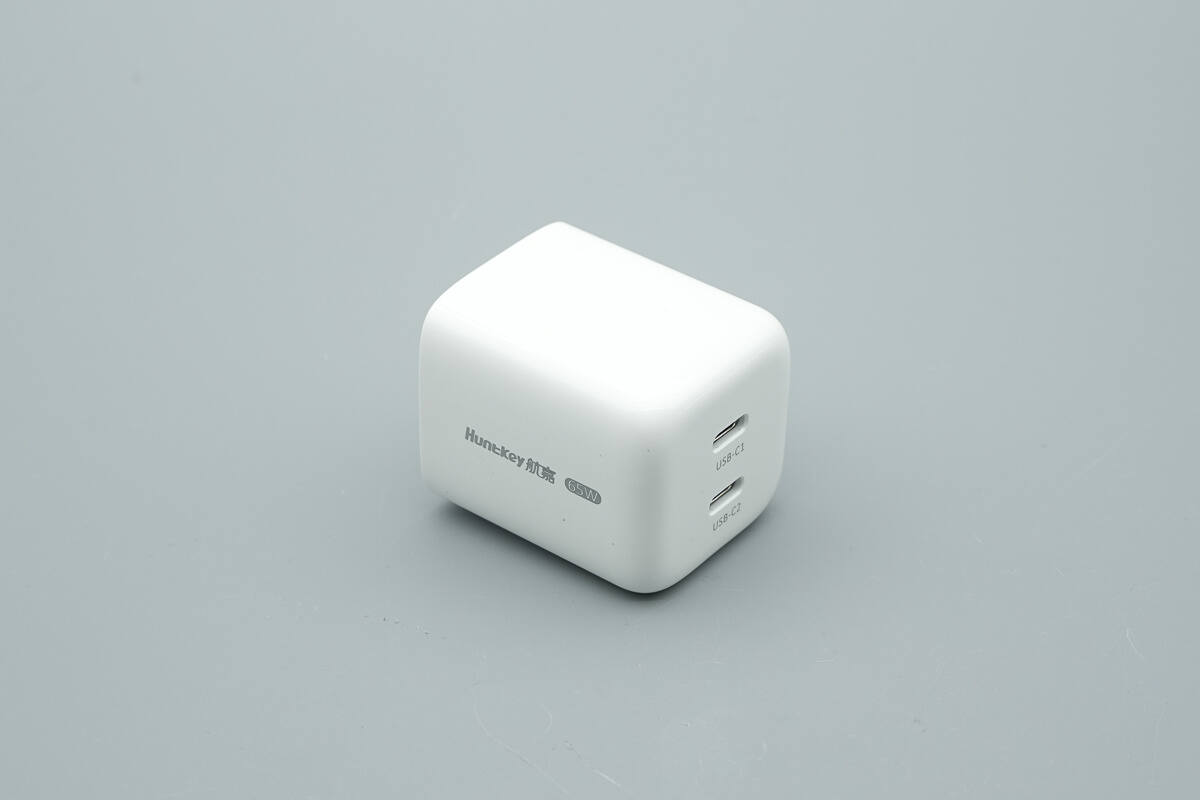
The enclosure is made of white flame-retardant material with a glossy finish, and the edges are smoothly rounded.
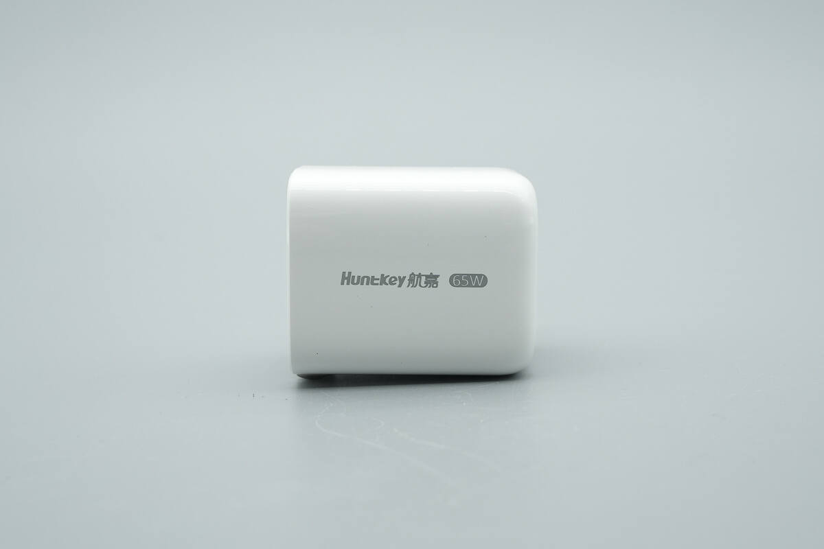
This side is marked with the HuntKey logo and the “65W” power rating.
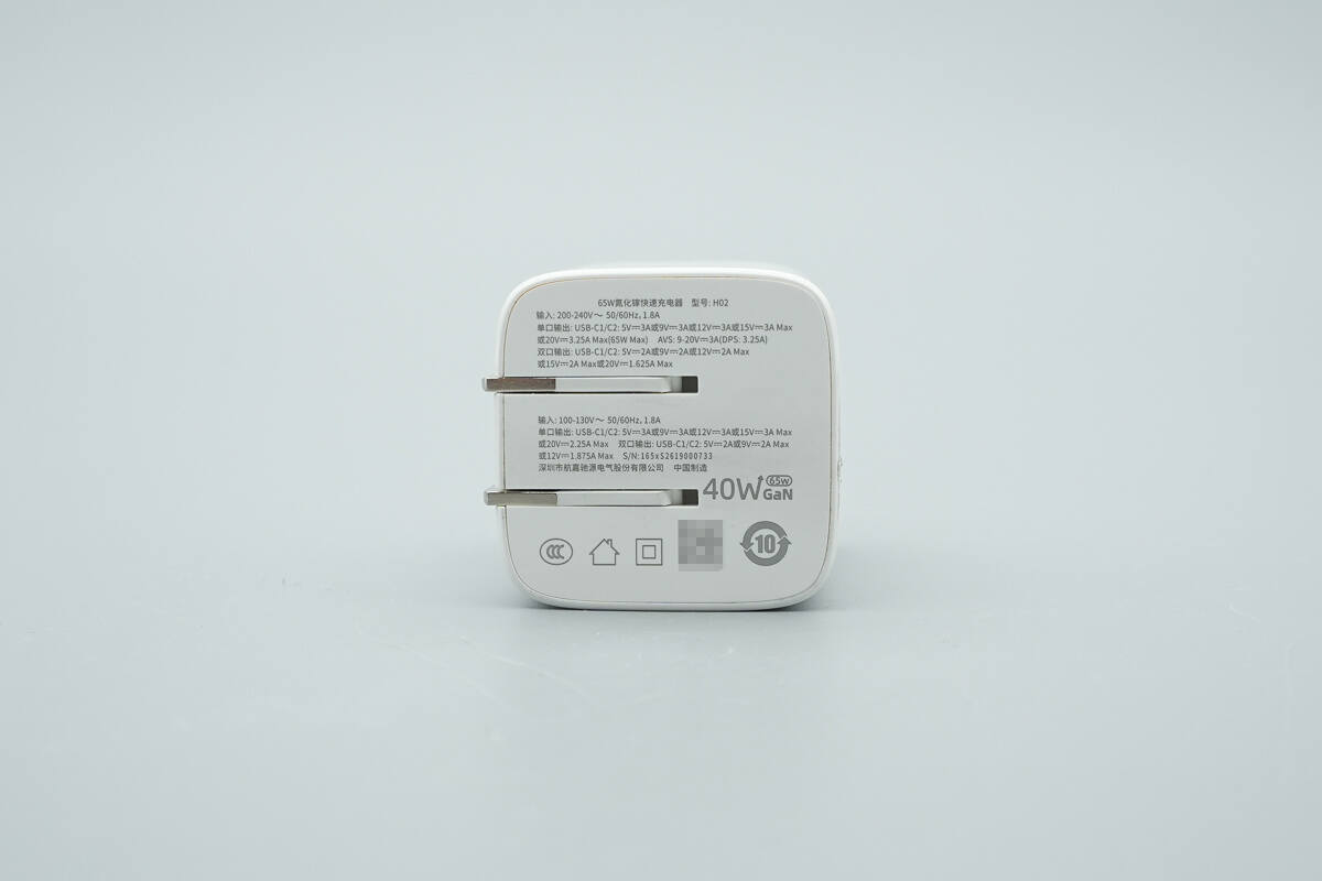
The bottom is printed with the technical specifications.
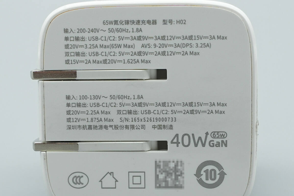
Model: H02
Input: 200-240V~ 50/60Hz, 1.8A
Single-port output:
USB-C1/C2: 5V3A, 9V3A, 12V3A, 15V3A, 20V3.25A Max (65W Max)
AVS: 9-20V3A (DPS: 3.25A)
Dual-port output:
USB-C1/C2: 5V2A, 9V2A, 12V2A, 15V2A, 20V1.625A Max
Input: 100-130V~ 50/60Hz, 1.8A
Single-port output:
USB-C1/C2: 5V3A, 9V3A, 12V3A, 15V3A, 20V2.25A Max
Dual-port output:
USB-C1/C2: 5V2A, 9V2A, 12V1.875A Max
The product has obtained CCC certification.
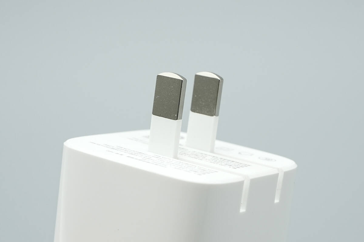
It is equipped with foldable plug pins.
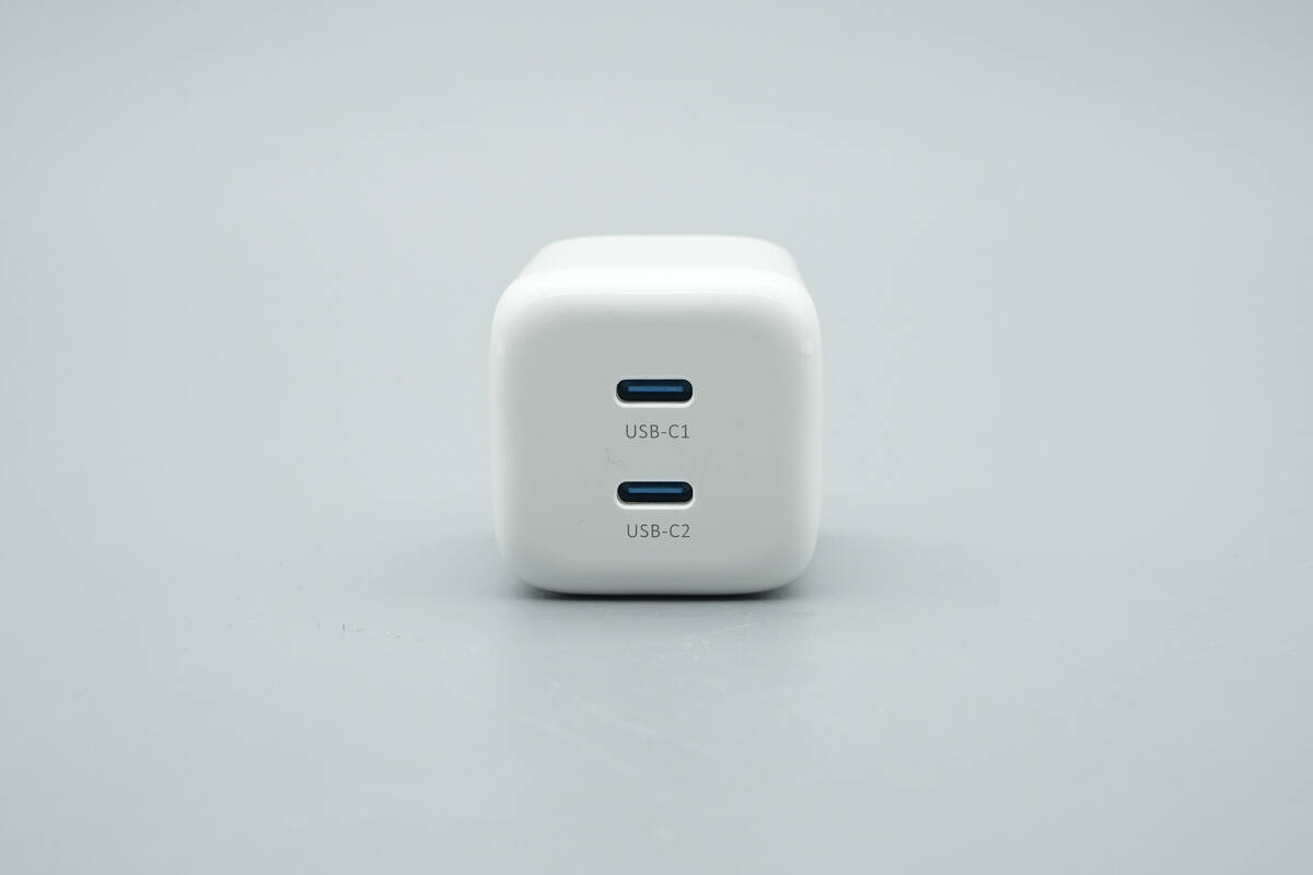
The top features dual USB-C ports, each labeled with its corresponding designation.
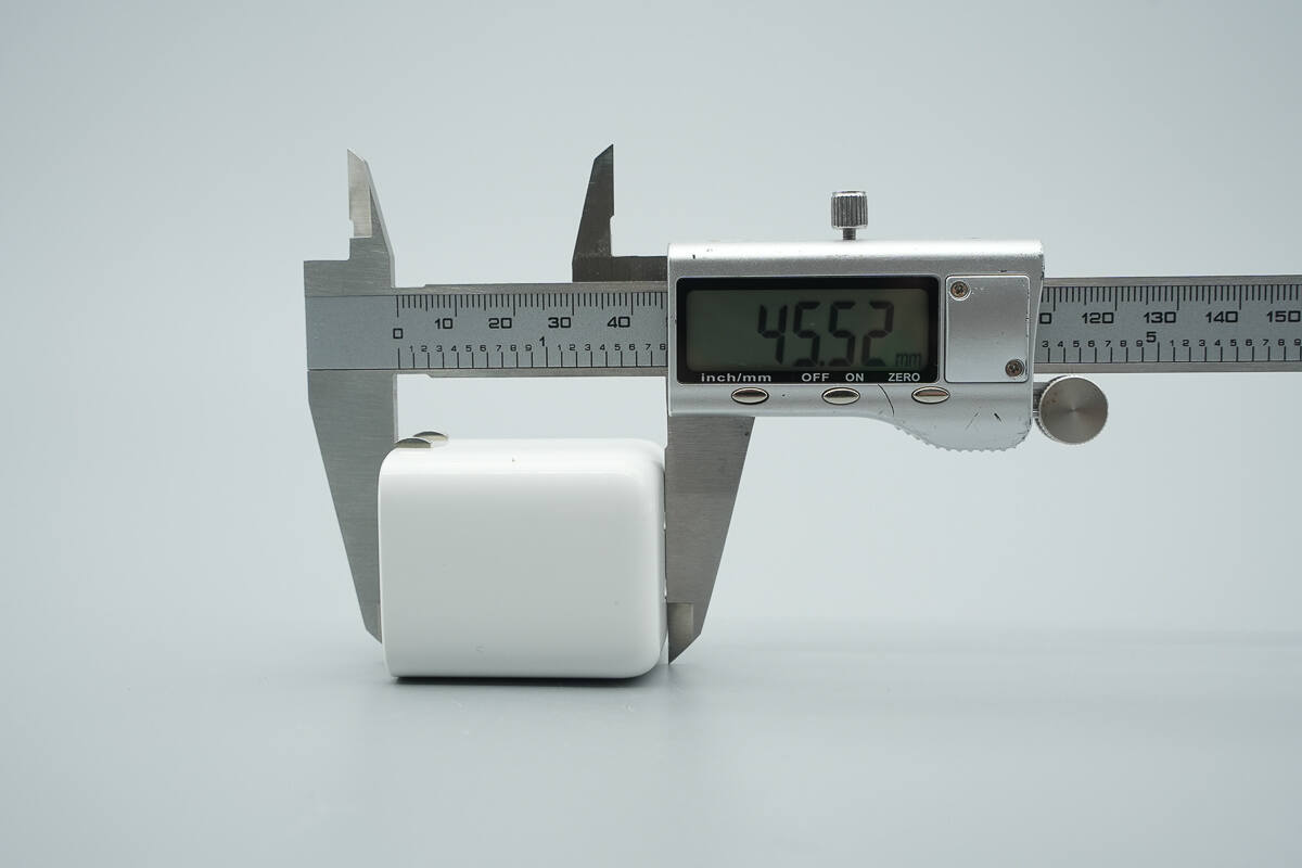
The length of the charger is about 45.52 mm (1.79 inches).
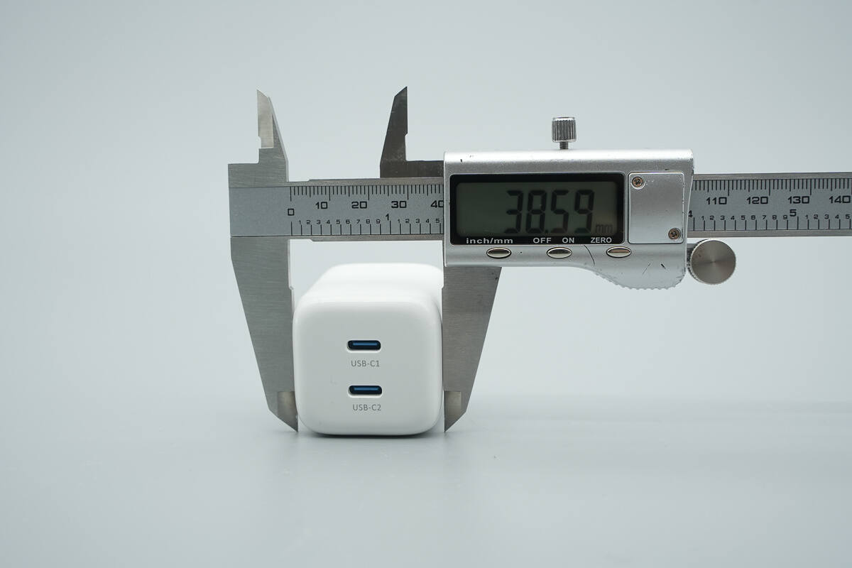
The width is about 38.59 mm (1.52 inches).
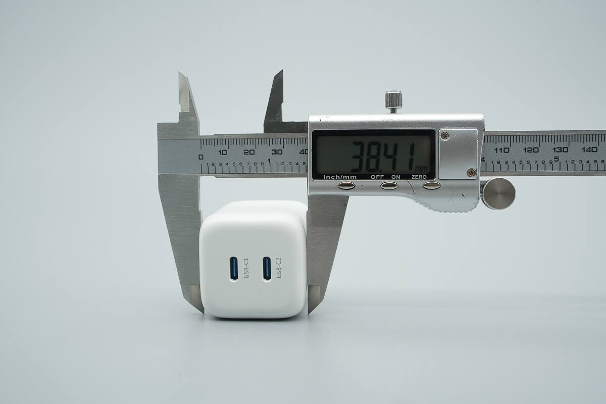
The thickness is about 38.41 mm (1.51 inches).
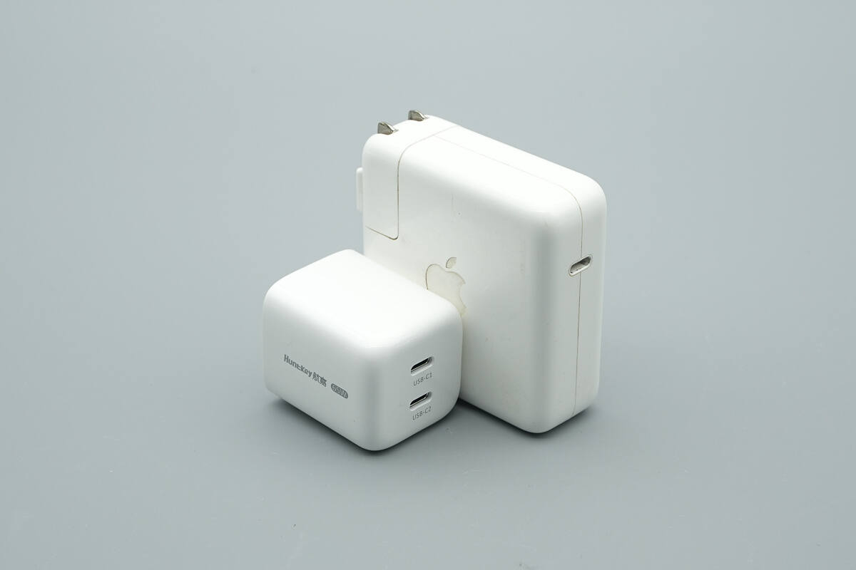
Compared with the Apple 67W charger, it has a clear size advantage.
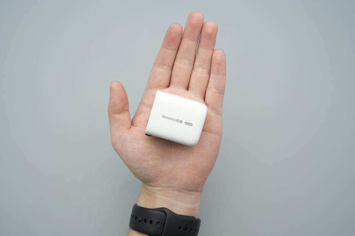
That's how big it is in the hand.
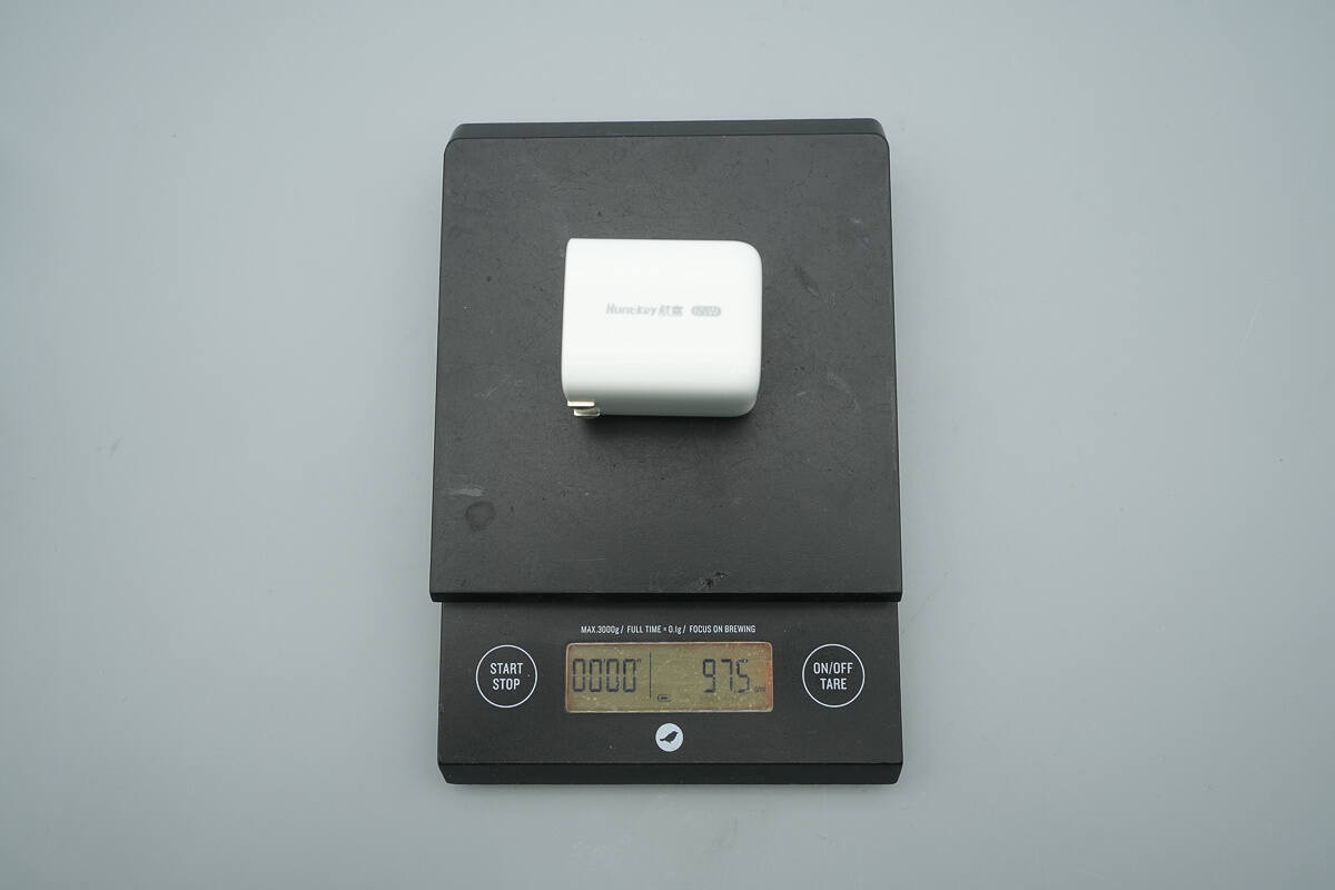
The weight is about 98 g (3.46 oz).
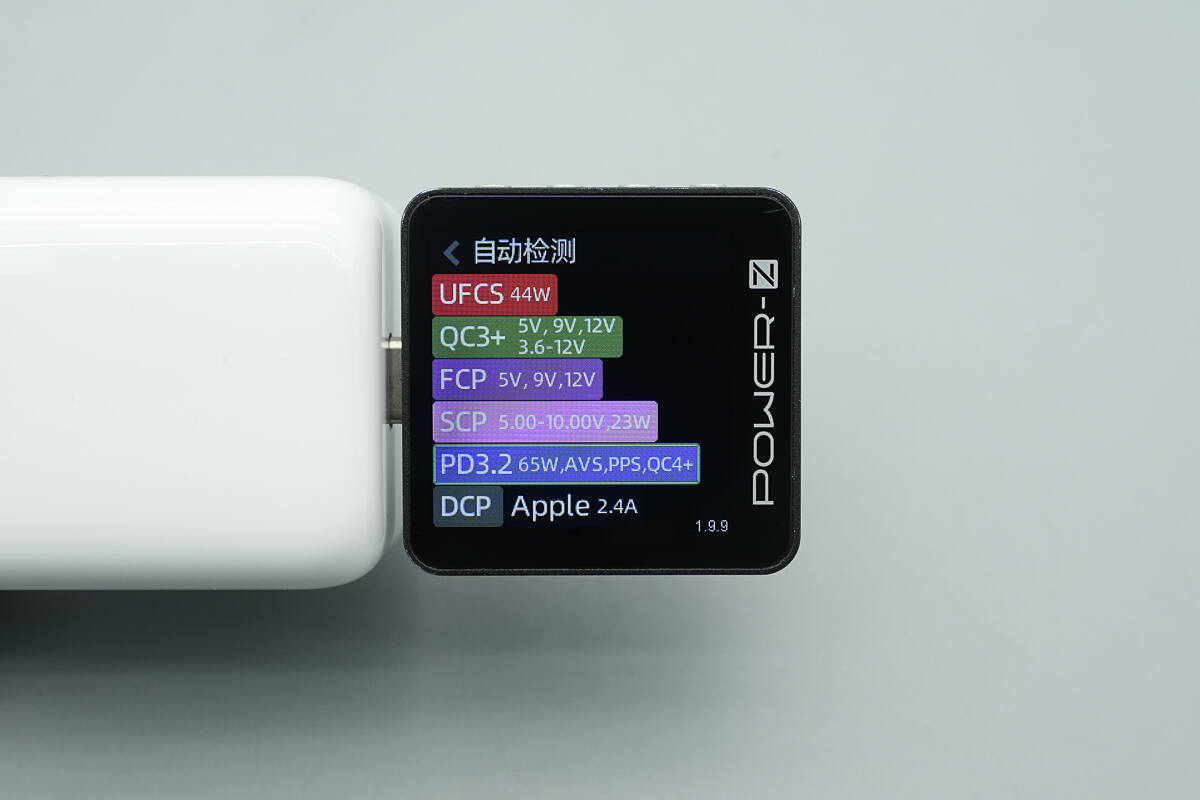
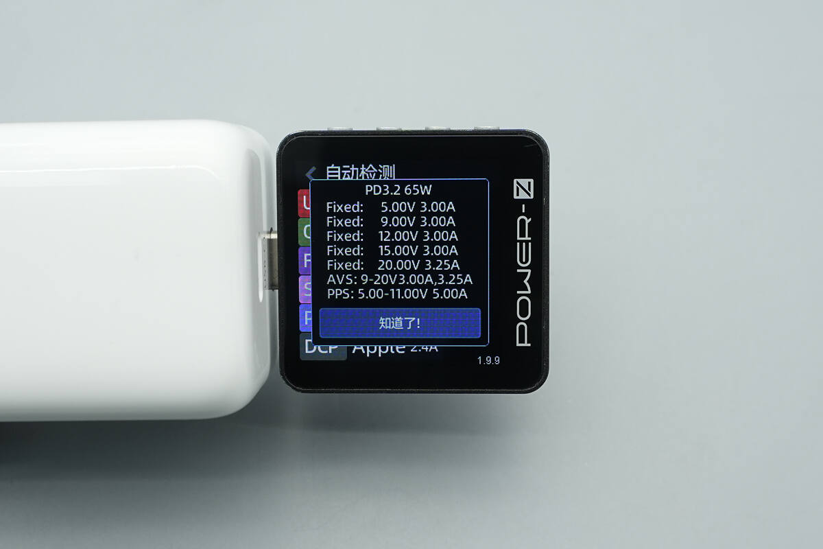
ChargerLAB POWER-Z KM003C shows that the USB-C1 supports QC3+/4+, FCP, SCP, PD3.2, PPS, DCP, and Apple 2.4A charging protocols.
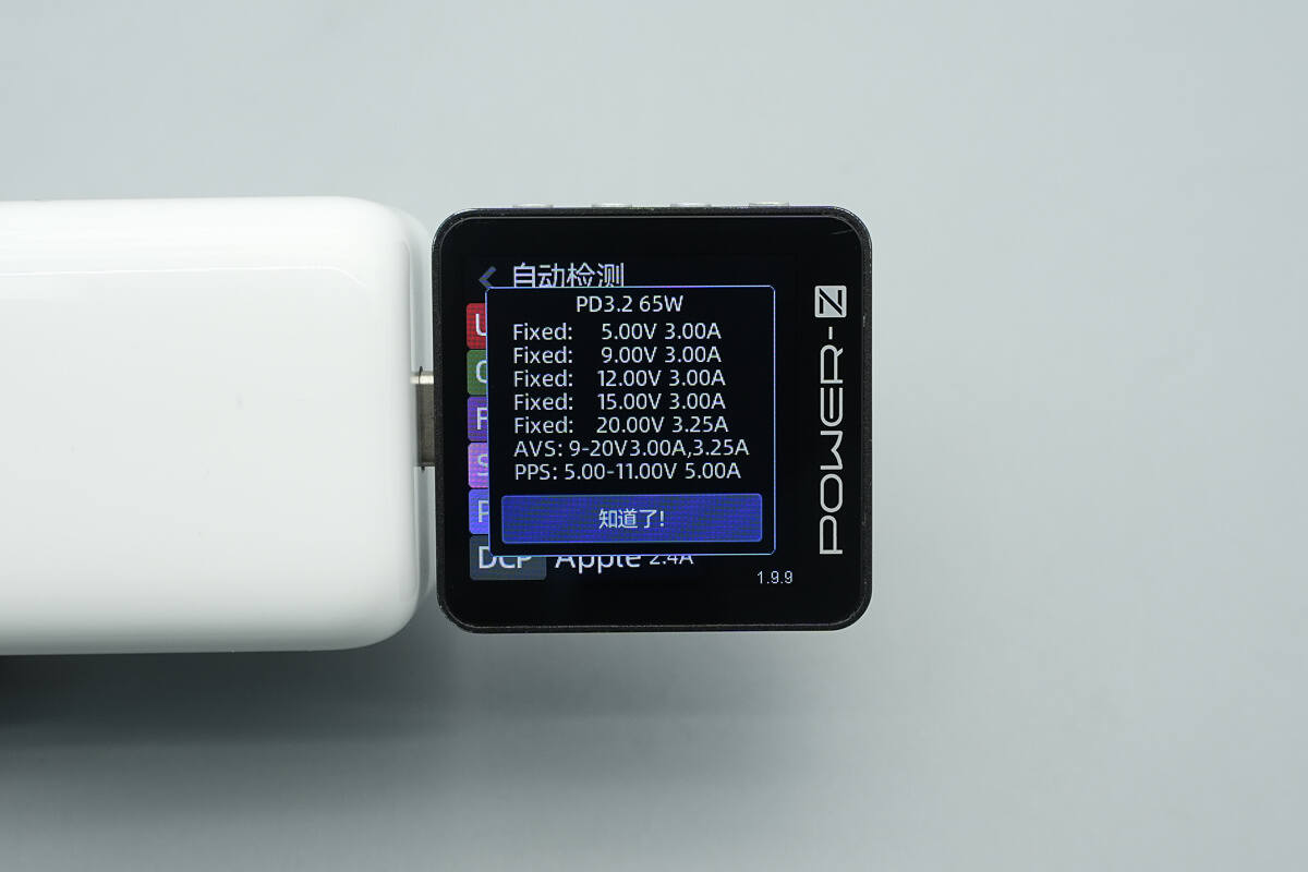
It features five fixed PDOs: 5V3A, 9V3A, 12V3A, 15V3A, and 20V3.25A, as well as AVS voltage ranges of 9-20V3A/3.25A and PPS voltage ranges of 5-11V5A.
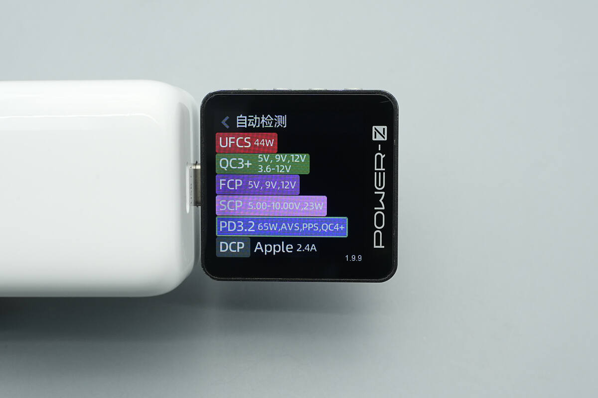
The USB-C2 port supports the same protocols as the USB-C1 port.
The PDO messages are also identical.
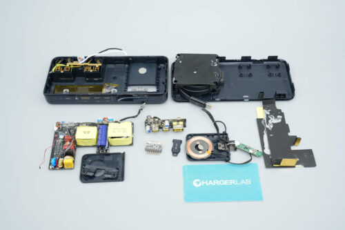
Teardown
Next, let's take it apart to see its internal components and structure.
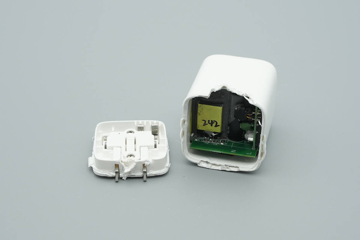
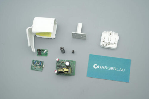
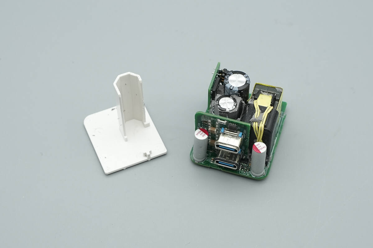
The ultrasonic-welded input-side casing was removed.
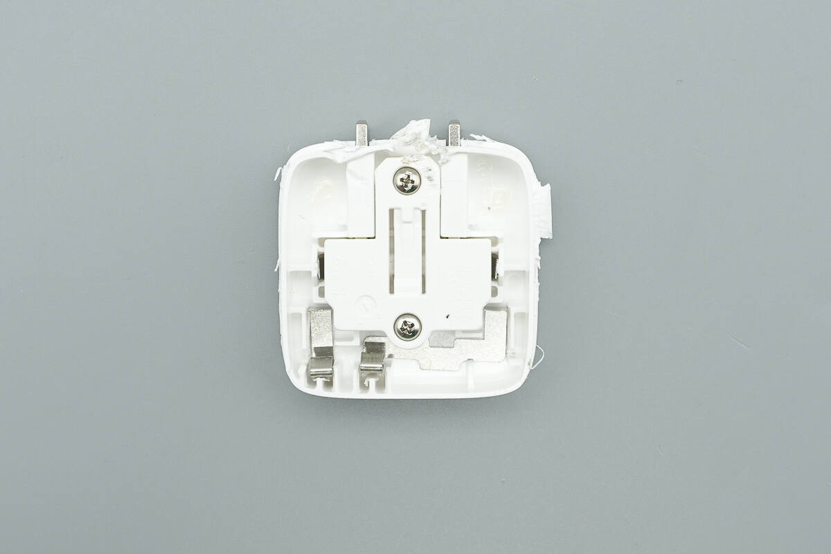
The plug pins are secured with a plastic plate and screws, making electrical contact with the PCBA module through metal plates.
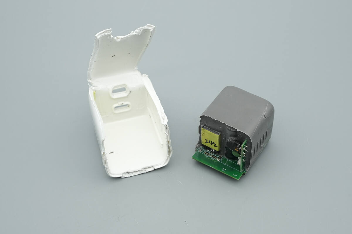
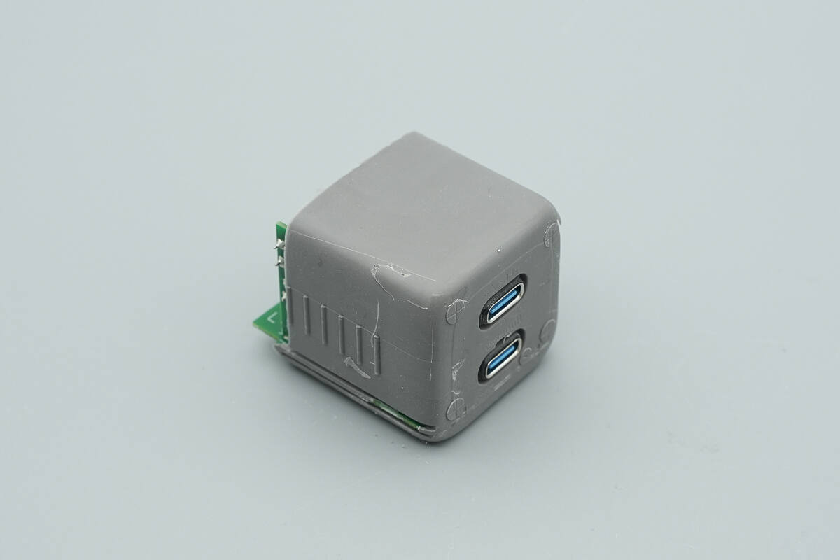
Remove the PCBA module.
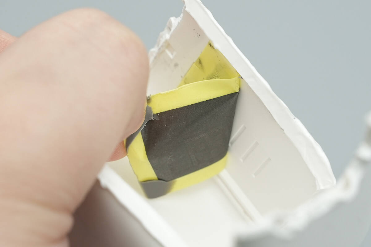
The inner side of the casing is lined with a graphite thermal pad and has been insulated.
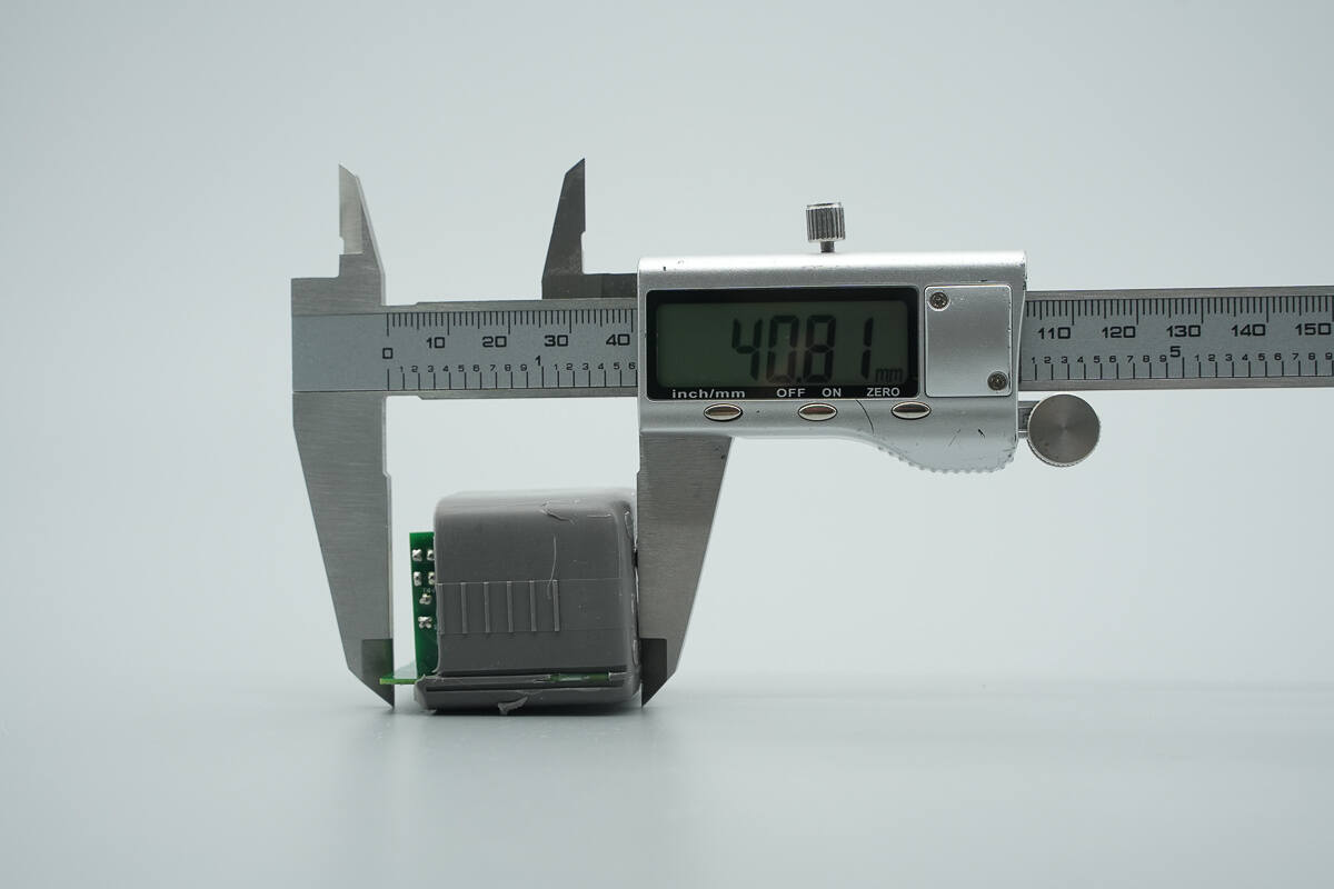
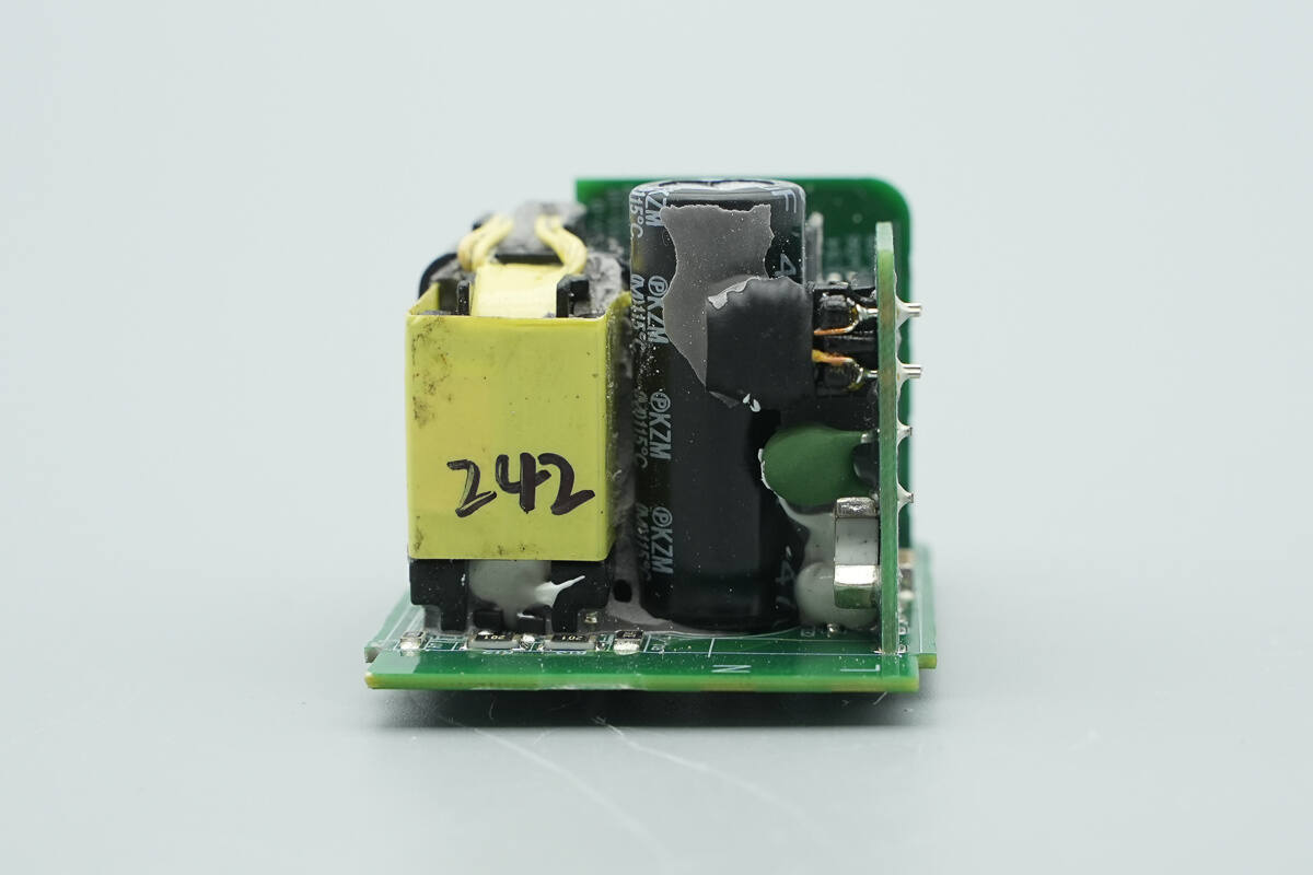
The length of the PCBA module is about 40.81 mm (1.61 inches).
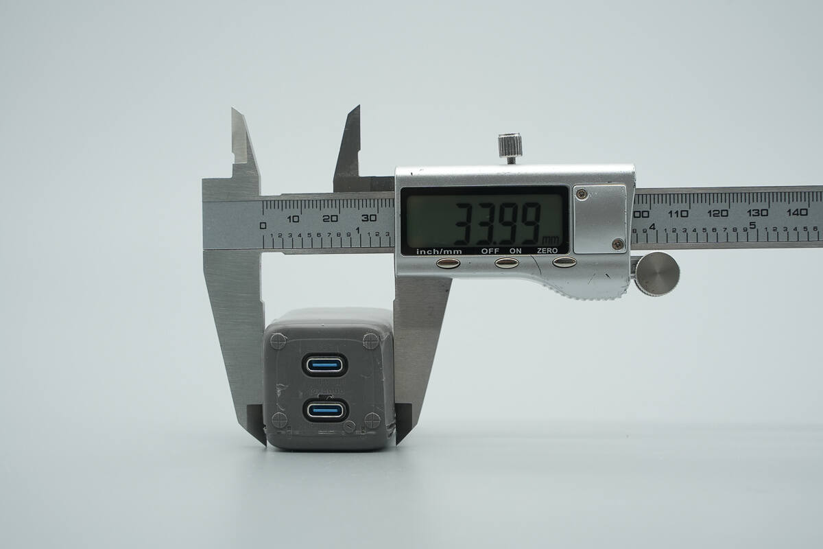
The width is about 33.99 mm (1.34 inches).
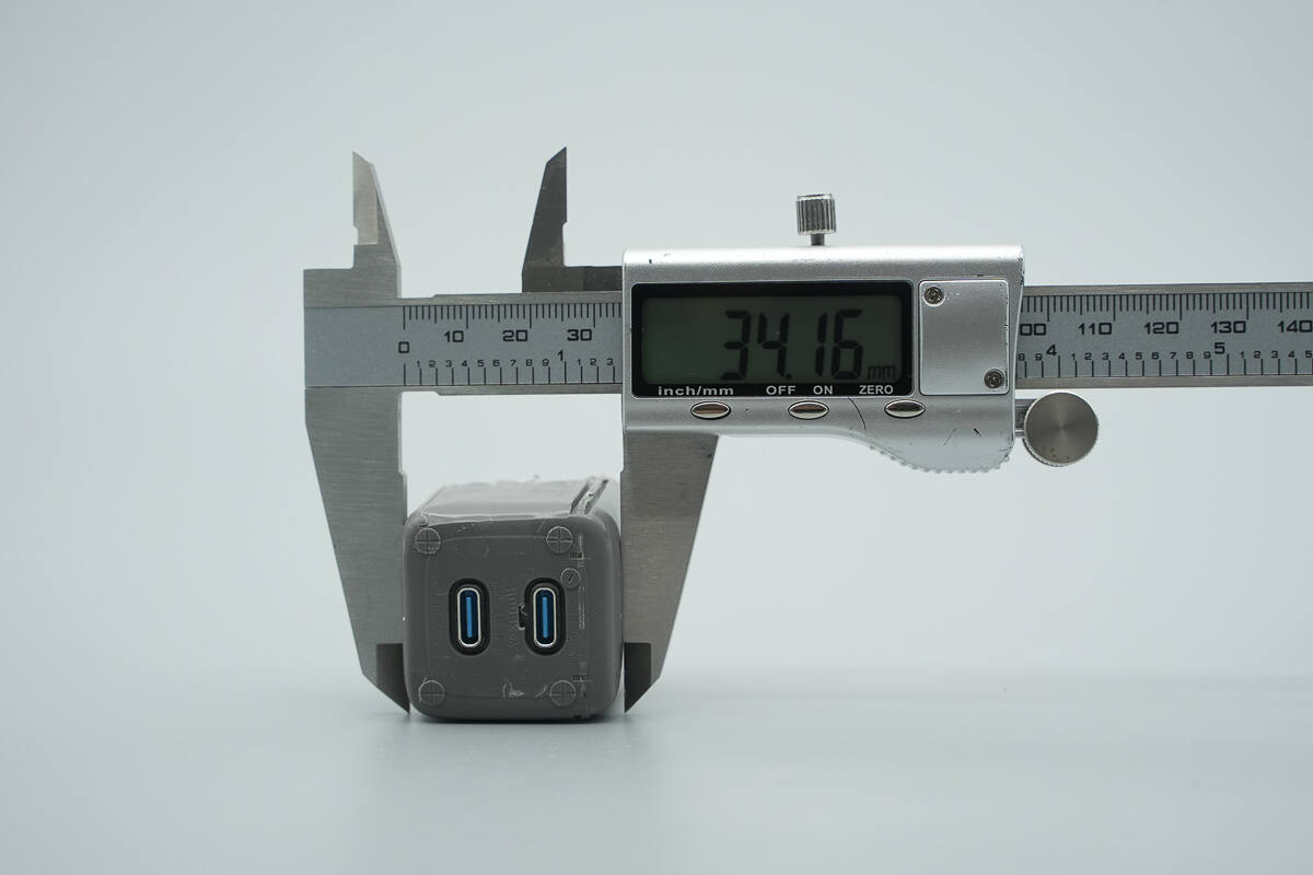
The thickness is about 34.16 mm (1.34 inches).
The PCBA module is encapsulated with potting, which enhances overall durability and thermal performance.
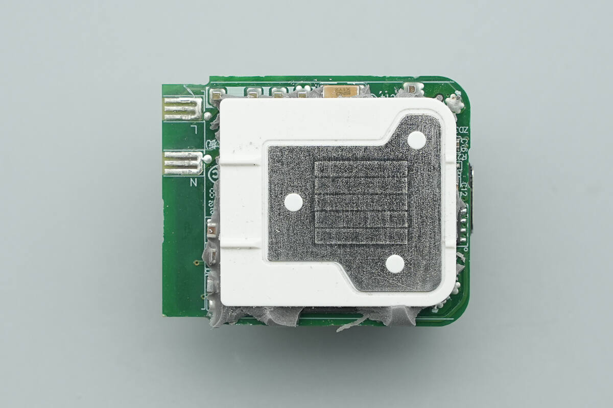
After removing the thermal adhesive, the bottom of the module is covered by a plastic plate and a heatsink.
After removing the plastic plate, the front side reveals an integrated capacitor isolation board.
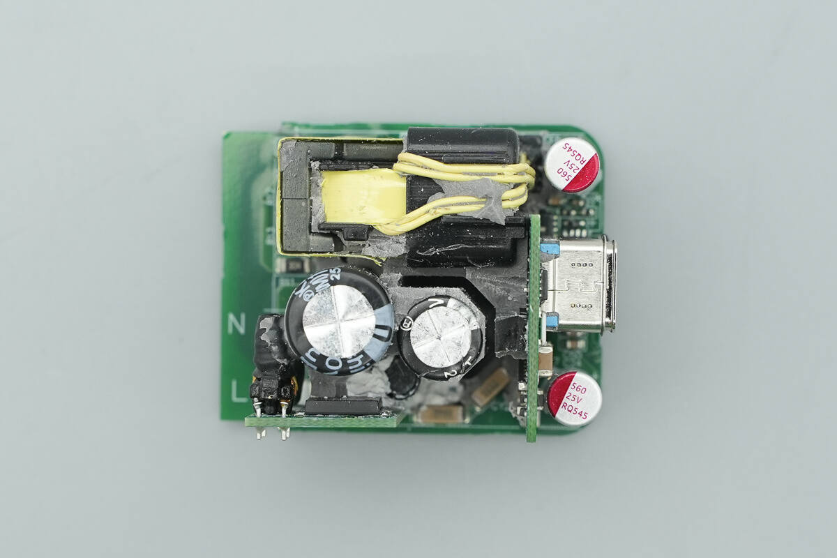
The front of the PCBA module houses filter capacitors and a transformer, while small PCBs are also positioned on the sides and at the output end.
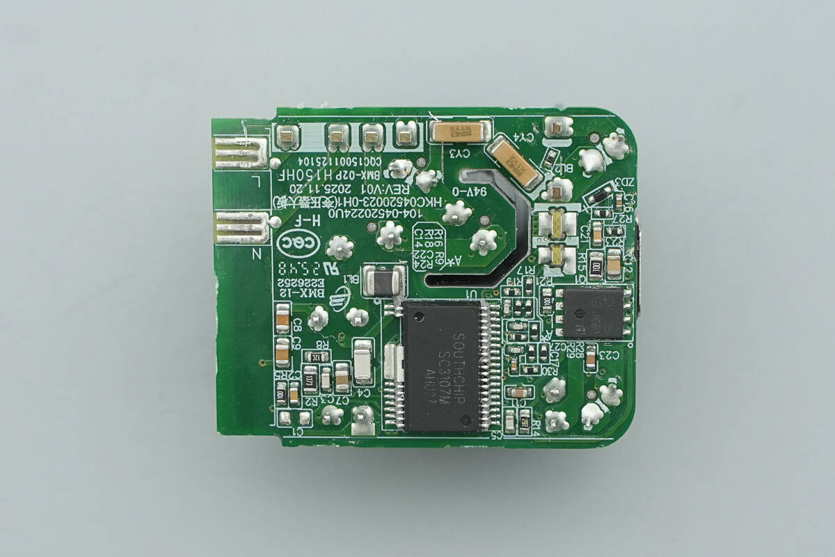
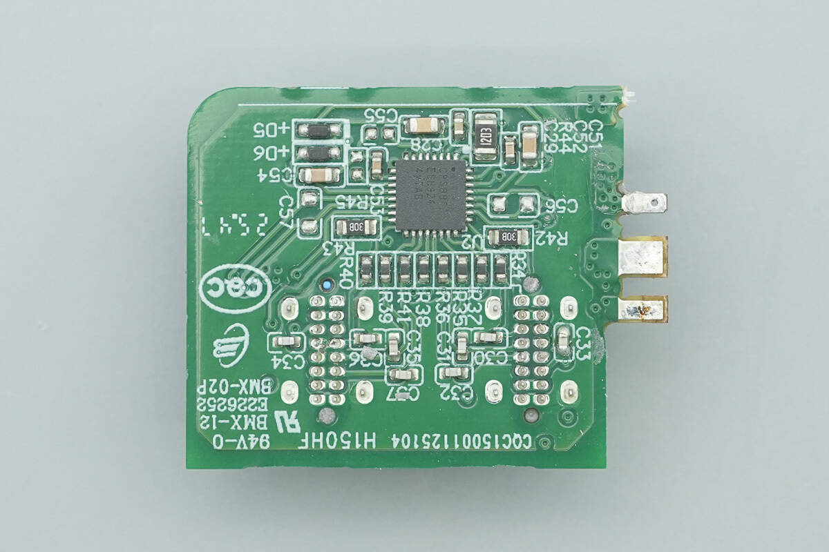
The back side features a master control chip and a synchronous rectifier.
On the front end of the PCBA module, the right side is soldered to the input PCB, with a high-voltage filter electrolytic capacitor positioned in the middle.
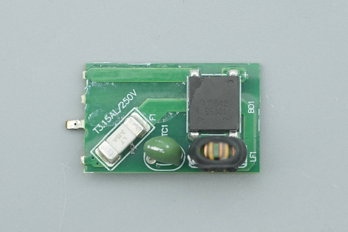
After removing the small PCB, the front side reveals a fuse, an NTC thermistor, a common mode choke, and a bridge rectifier.
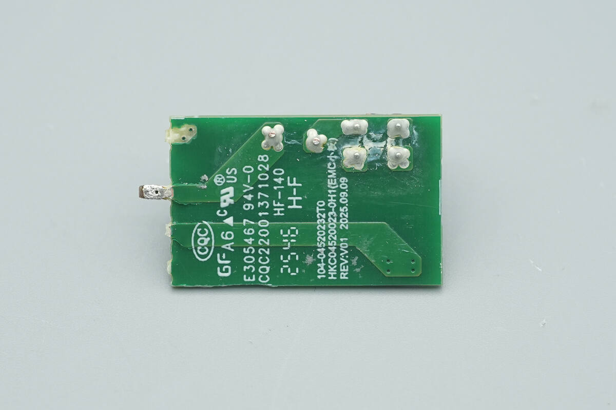
The back side has no components.
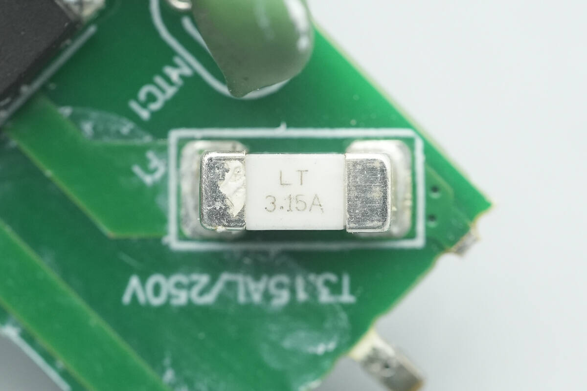
The Y-capacitor is rated for 3.15A.
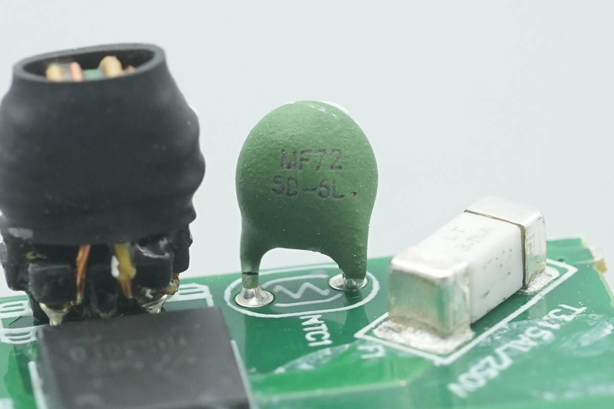
The NTC thermistor is used to suppress inrush current at power-on.
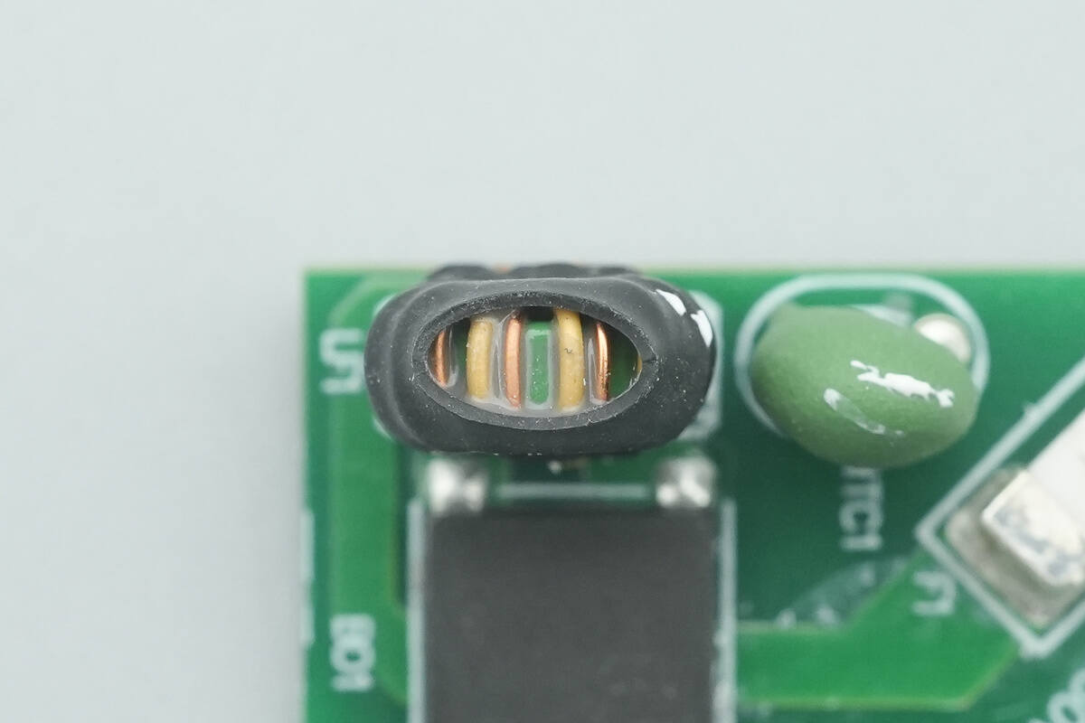
The common mode choke is used to suppress EMI interference and is insulated with a heat-shrink tube.
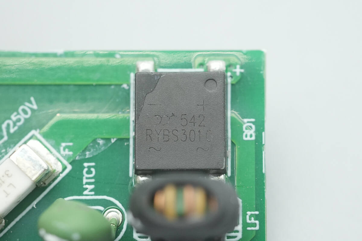
The bridge rectifier is from YJ, model RYBS3010. It is a fast-recovery bridge rectifier with a rating of 3A/1000V, housed in a YBS package.
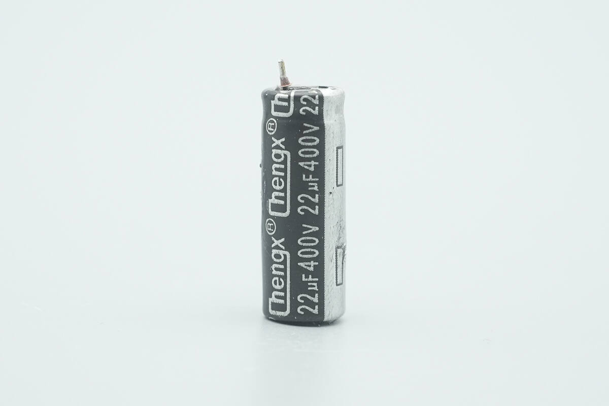
The high-voltage filter electrolytic capacitor is from Chengx, with a specification of 400V 22μF.
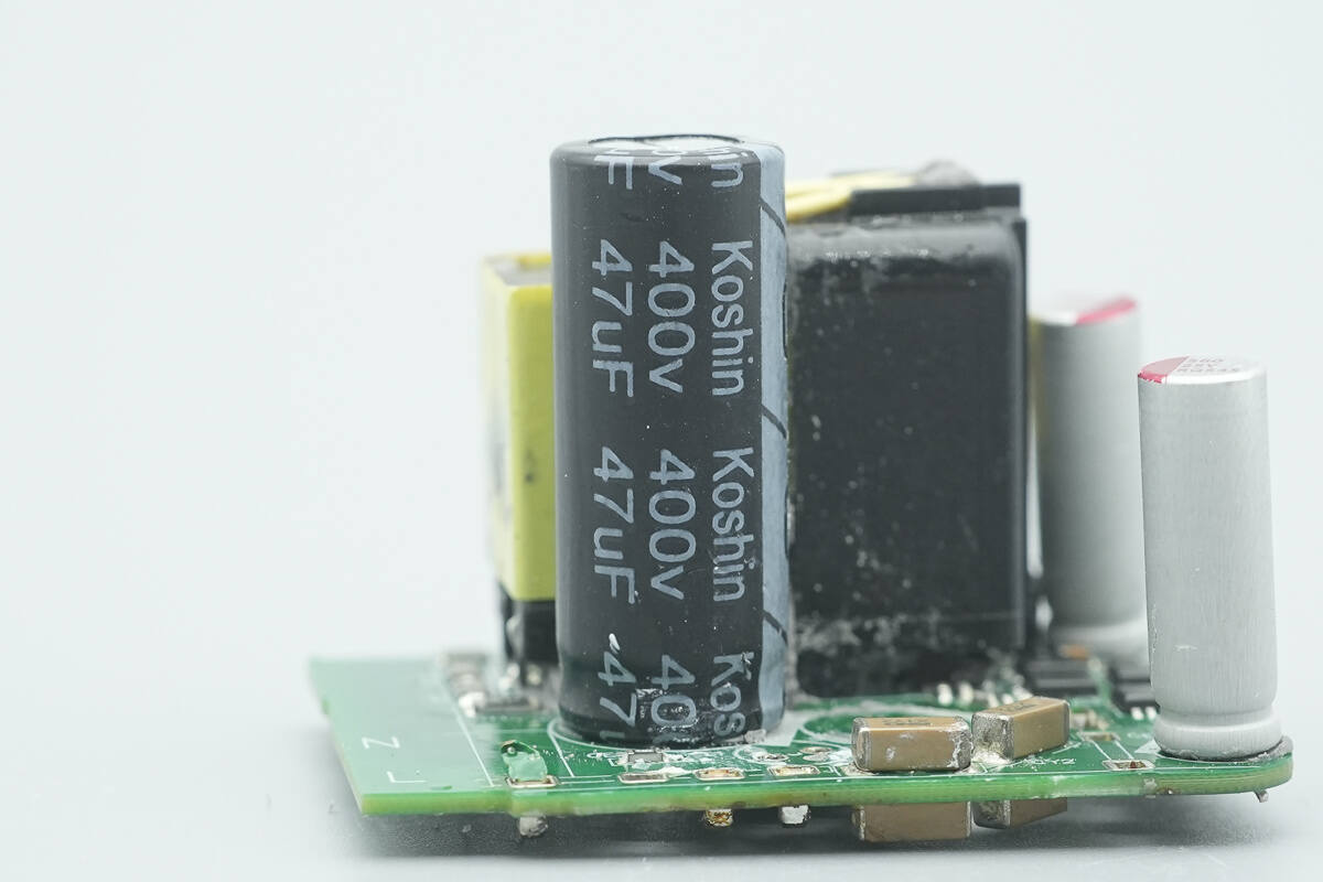
Another high-voltage filter electrolytic capacitor is from Koshin, with a specification of 400V 47μF.
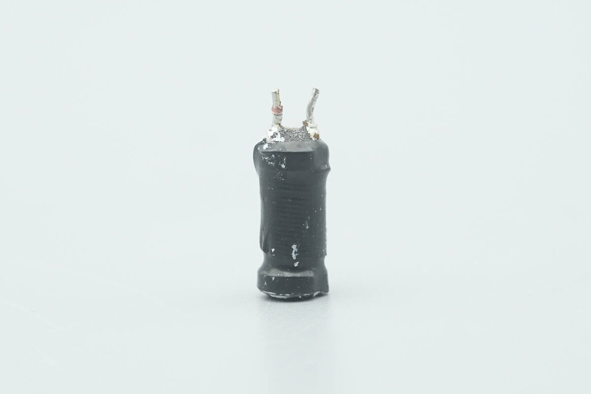
Close-up of the I-shaped inductor.
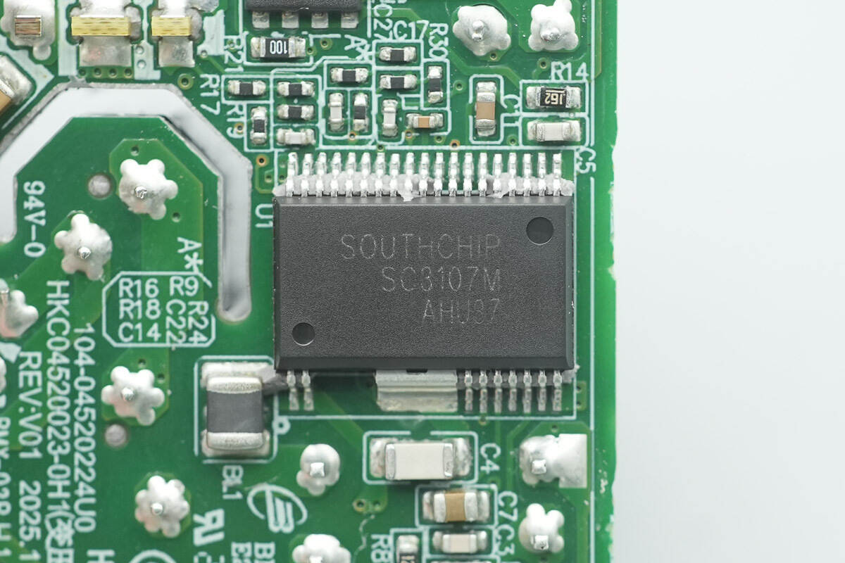
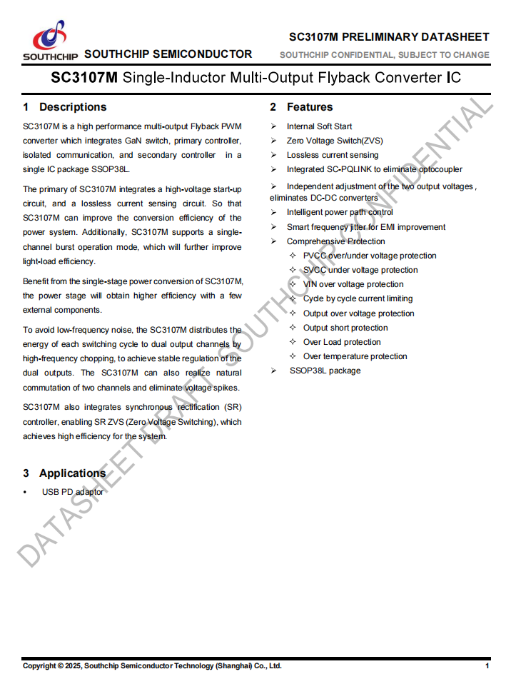
The master control chip is from SouthChip, model SC3107M. It features SouthChip’s fully integrated high-voltage isolation package, which includes a primary controller, high-voltage GaN power transistor, high-speed isolated communication, secondary synchronous rectification controller, and high-frequency switching MOS driver.
The high integration of the SC3107M significantly reduces the number of peripheral components in the charger and can replace multiple discrete chips in traditional power solutions, enabling a more compact power design. It offers advantages such as shorter development cycles and higher cost-performance for products.
The SC3107M integrates a high-speed digital isolation communication module, SC-PQLINK®, which not only provides higher system reliability compared to optocouplers but also enables precise secondary-side control.
Leveraging secondary-side control, it supports primary-side zero-voltage switching (ZVS) and active synchronous rectification, significantly improving overall power efficiency and reducing thermal requirements. The chip’s unique dual-output channel independent regulation allows stable adjustment and natural commutation of two outputs through high-frequency chopping, eliminating voltage spikes without additional DC-DC converters.
The SC3107M also incorporates advanced features such as soft-start, intelligent frequency dithering, smart power path control, and lossless current sensing. It provides comprehensive protection mechanisms, including PVCC over/under-voltage protection, SVCC under-voltage protection, VIN over-voltage protection, cycle-by-cycle current limiting, output over-voltage protection, short-circuit protection, overload protection, and over-temperature protection. Packaged in SSOP38L, it is well-suited for high-performance, multi-output fast-charging power designs.
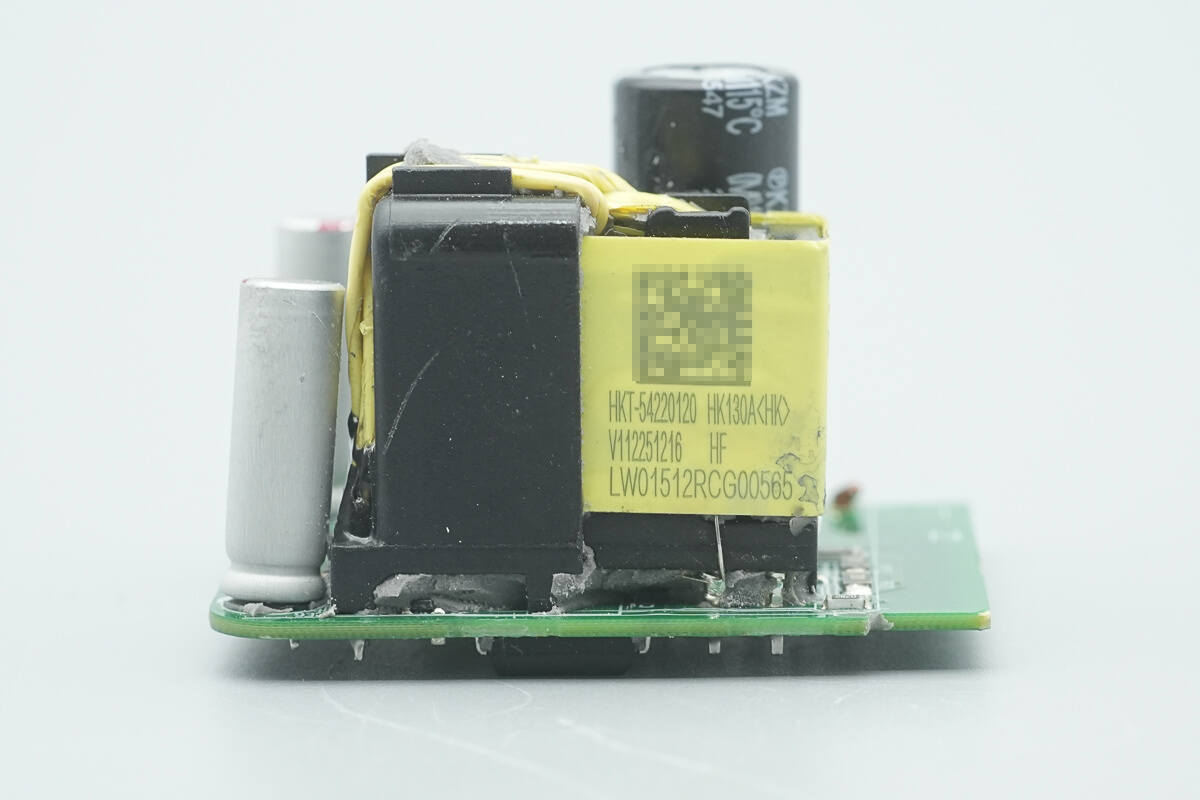
Close-up of the transformer.
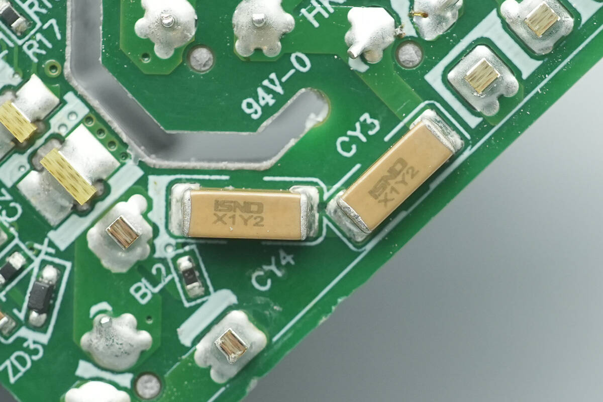
The two SMD Y-capacitors are from ISND.
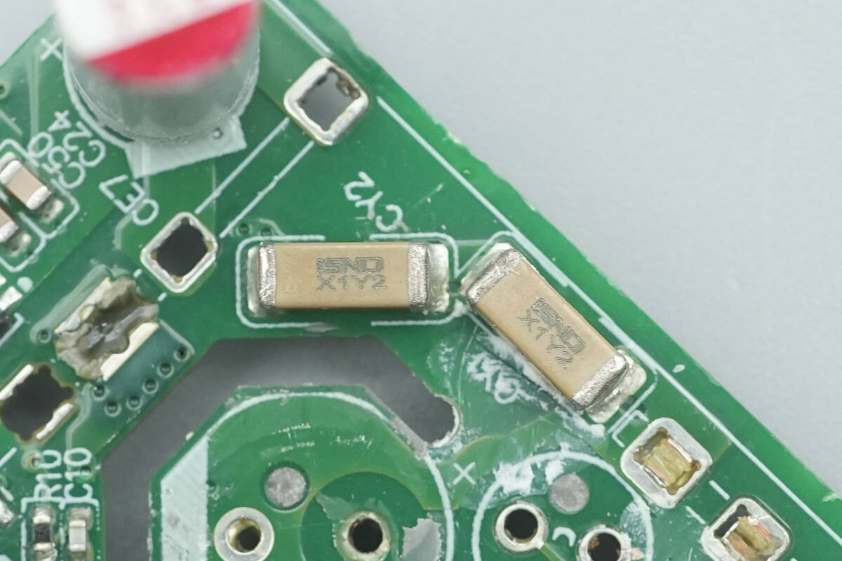
A close-up of the two capacitors on the other side; they are connected in series in pairs to enhance safety ratings.
At the output end, solid capacitors are soldered on both sides.
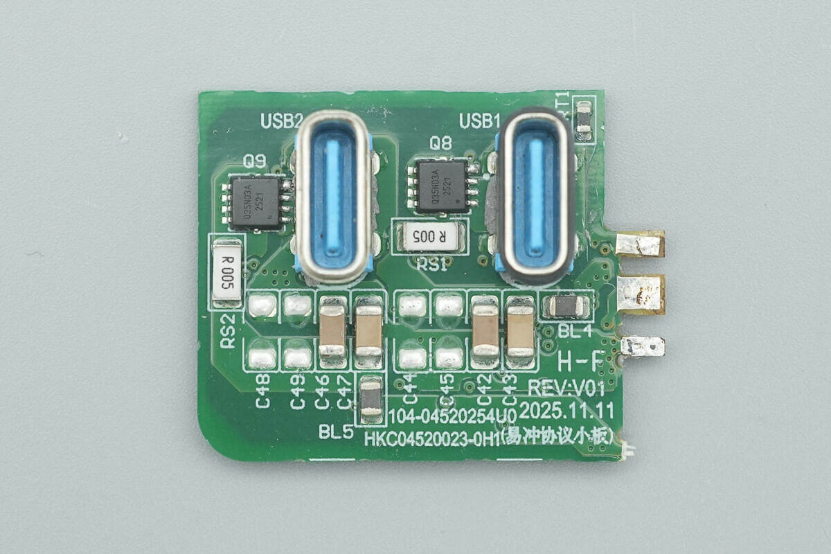
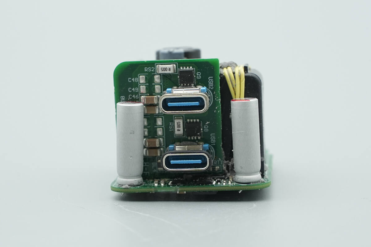
After removing the output-end PCB, the front side reveals the VBUS MOSFETs.
The back side is equipped with the protocol chip.
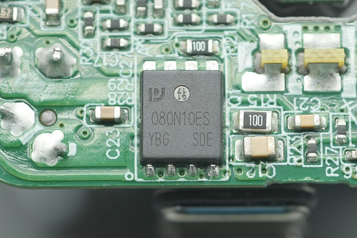
The synchronous rectifier is from PY, model PW080N10ES. It is an NMOS with a voltage rating of 100V and an on-resistance of 6.5 mΩ, housed in a DFN 5×6 package.
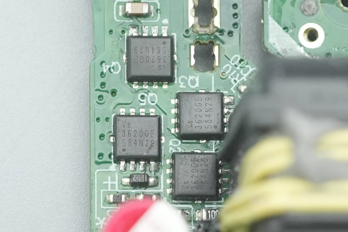
The four switching MOSFETs are from Vergiga, model VS3620GEMC. They are NMOS with a voltage rating of 30V and an on-resistance of 4.9 mΩ, housed in a PDFN3333 package.
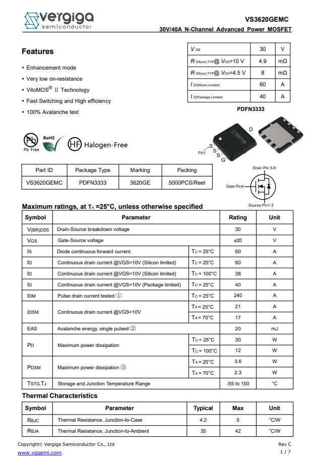
Here is the information about Vergiga VS3620GEMC.
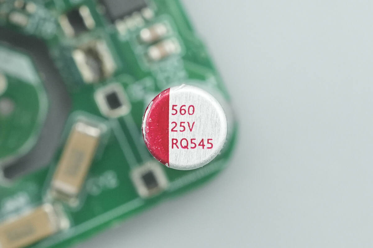
The solid capacitor is rated at 25V 560μF.
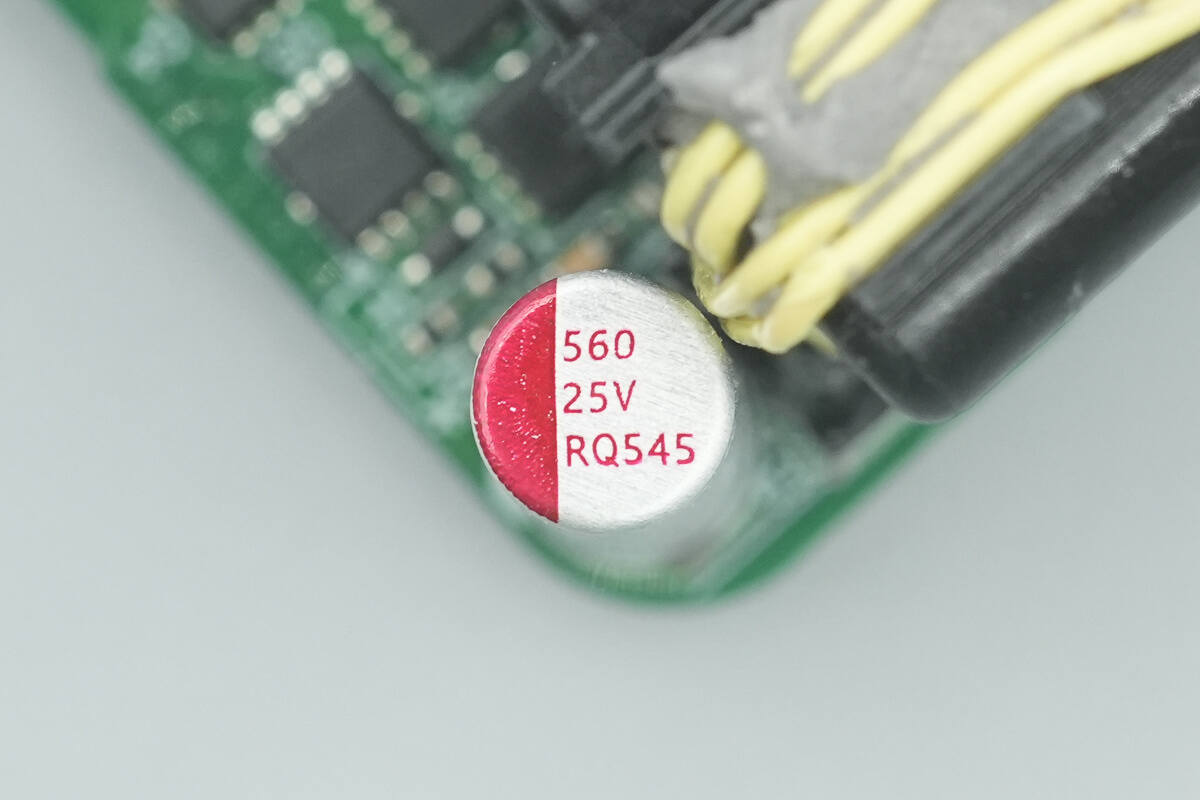
The other solid capacitor has the same specification.
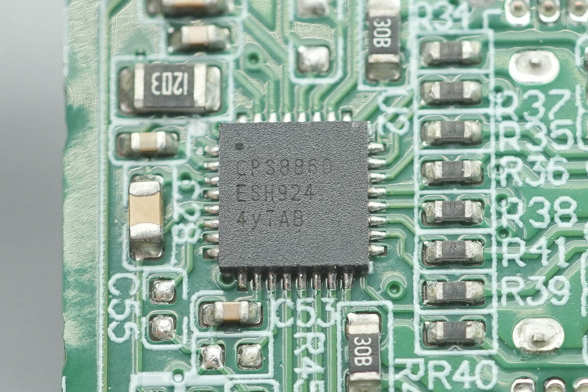
The protocol chip is from CPS, model CPS8860. It is a highly integrated fast-charging protocol controller featuring dual-port fast-charging output, dual-port management logic, and power-sharing capabilities. It supports PD3.1, QC2.0/3.0, UFCS, SCPA/B, AFC, Apple, and BC1.2 CDP, covering the mainstream fast-charging protocols on the market. With minimal external components, it enables the construction of an efficient and superior multi-protocol dual-port charging solution.
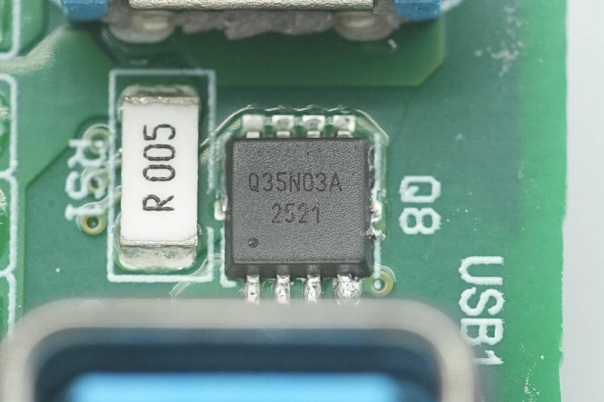
The VBUS MOSFETs for both ports are marked Q35N03A and are housed in PDFN3333-8L packages.
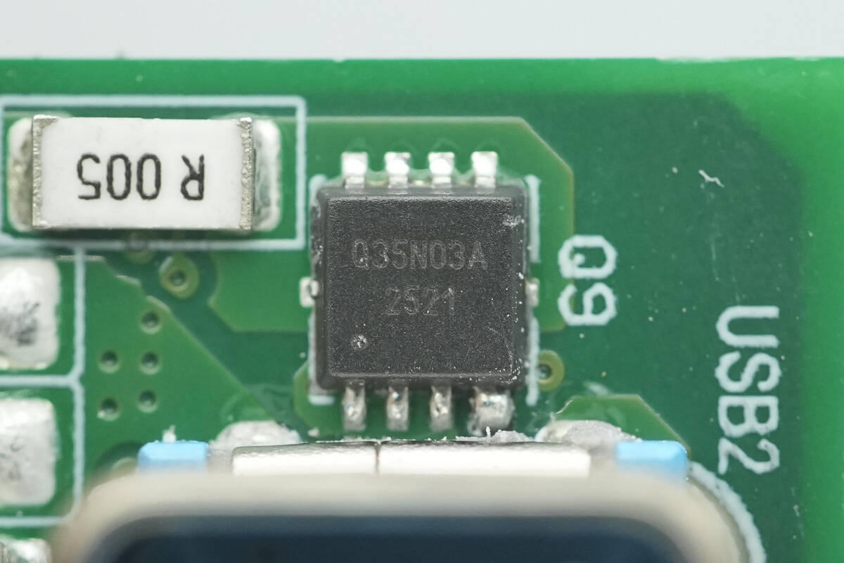
Close-up of the other VBUS MOSFET.
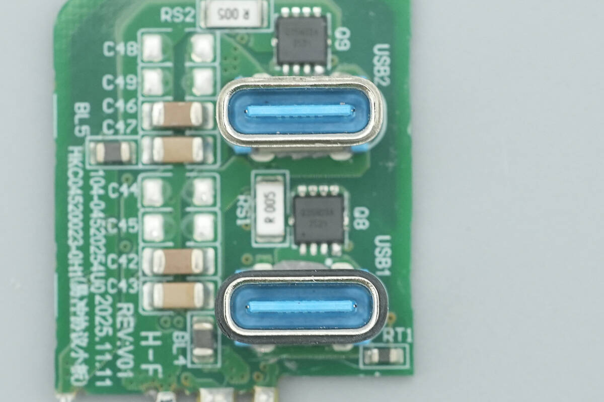
Close-up of the two USB-C sockets.

Well, those are all components of the HuntKey 65W Dual USB-C GaN Charger.
Summary of ChargerLAB
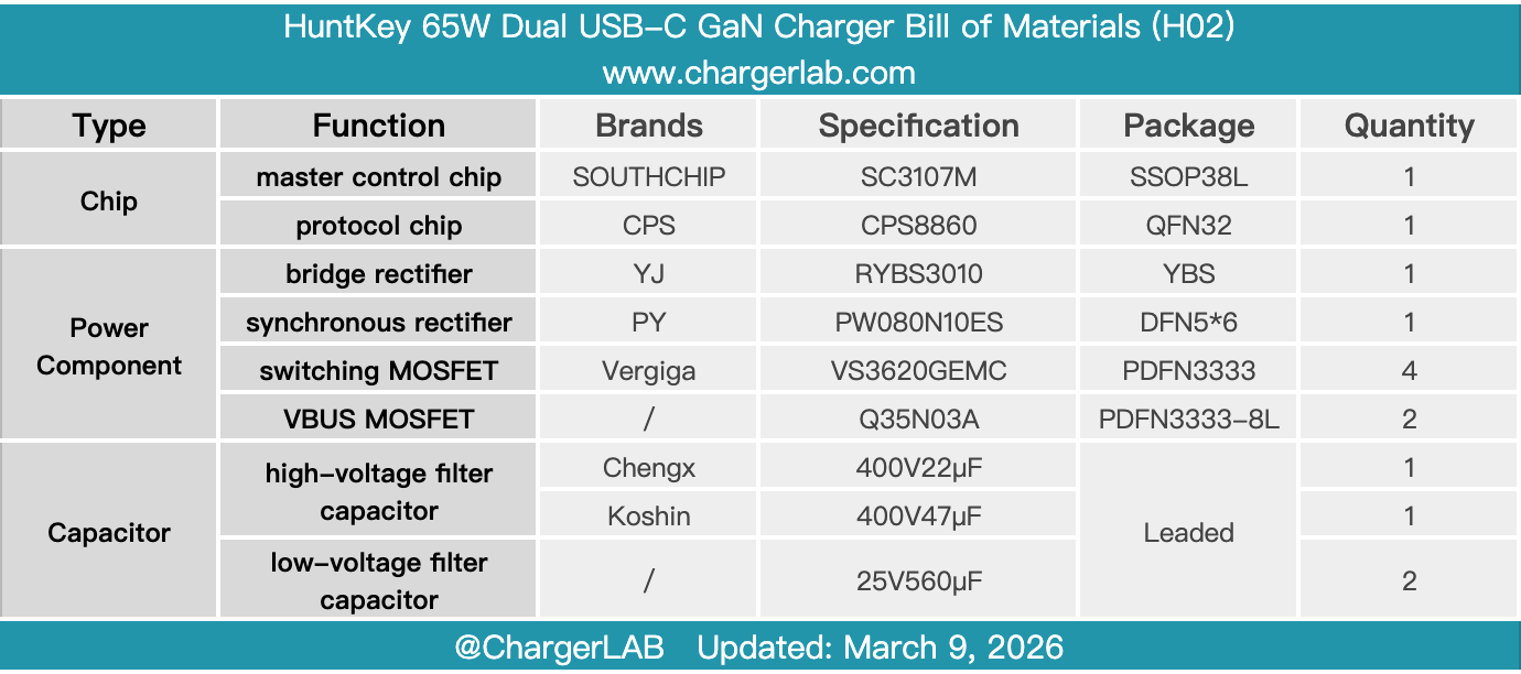
Here is the component list of the HuntKey 65W Dual USB-C GaN Charger for your convenience.
Its design is simple and practical, featuring a glossy body with foldable plug pins for compact portability. It supports 65W output and is compatible with PD3.2, PPS, and other protocols. The dual-port blind-plug design also provides great convenience for everyday use.
After taking it apart, we found that it uses the SouthChip highly integrated master control chip SC3107M, which greatly simplifies the peripheral circuitry. Combined with the chip’s primary-side zero-voltage switching and active synchronous rectification features, it significantly enhances overall system reliability, efficiency, and power density, while also reducing thermal requirements.
It uses the CPS CPS8860 protocol chip to achieve dual-port fast-charging control and power distribution. The PCBA module is treated with potting, effectively enhancing durability and thermal performance. The interior of the casing is lined with a graphite thermal pad, further improving heat dissipation. Overall, the product performs excellently in terms of size management, protocol compatibility, and internal build quality and materials, making it a high-quality fast-charging solution that combines practicality with advanced technology.
Related Articles:
1. Teardown of Samsung 60W Low Standby GaN Charger (EP-T6010)
2. Teardown of MORNSUN 550W Platinum SiC Server Power Supply (LMS550-P12B)
3. Teardown of Apple 40W Dynamic Power Adapter (A3365, HK Version)