Introduction
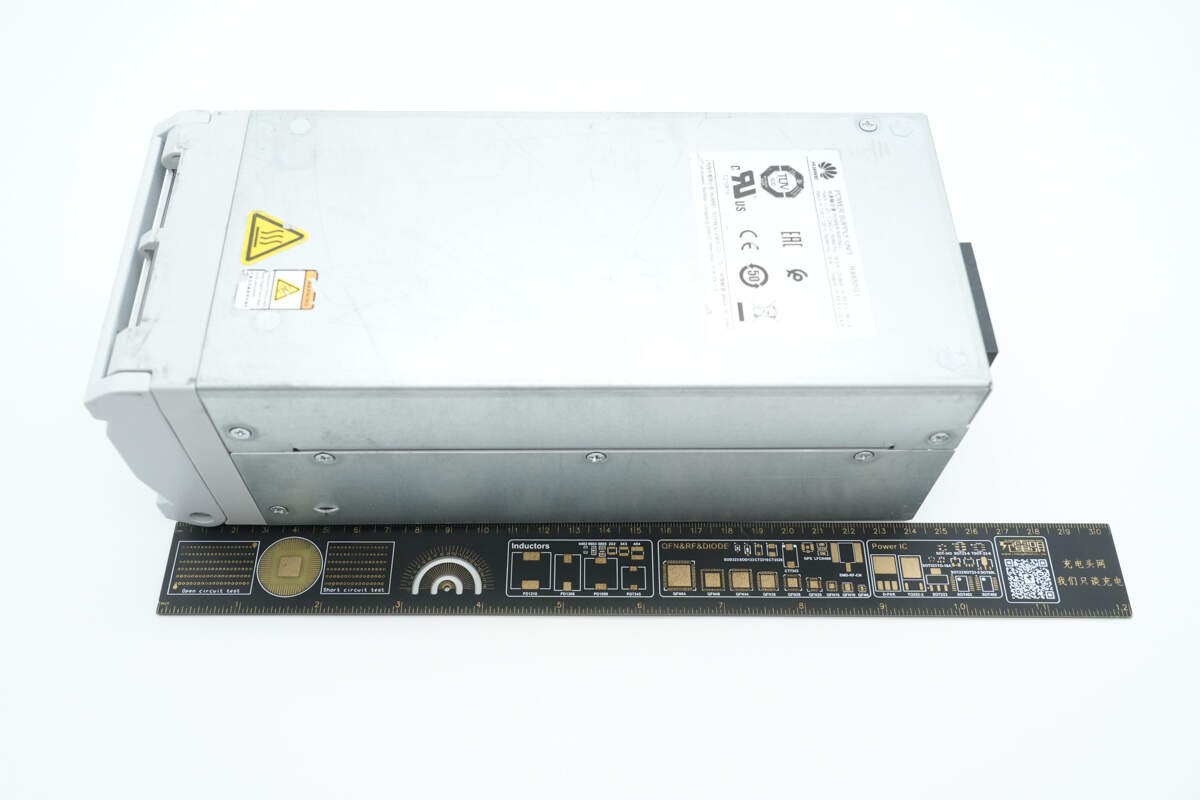
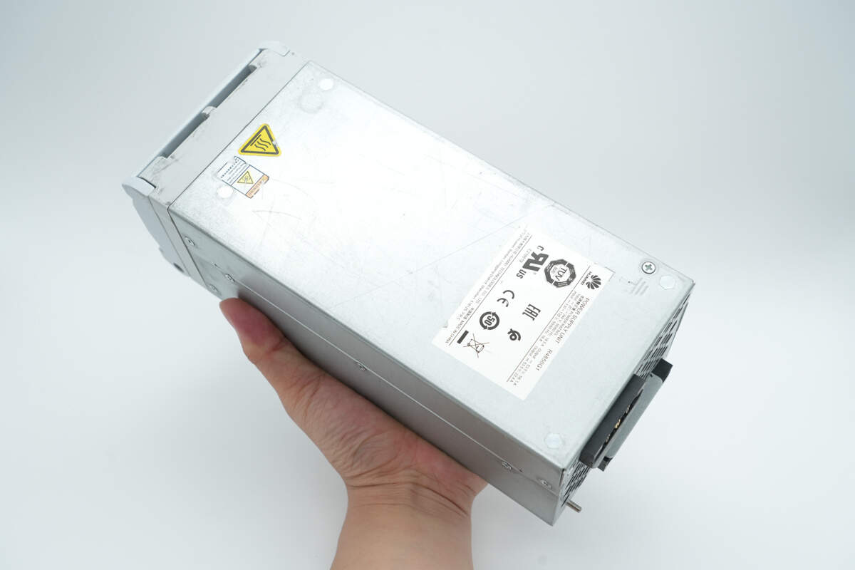
Recently, we obtained the Huawei R4850G1 power supply. This module features digital control and supports a wide range of input voltages. Its default output voltage is 53.5V, with a rated output power of 3000W. When the input voltage is low, the output power is limited to 1200W. The rear of the module is equipped with connectors for input, output, and communication connections.
The front has mounting clips and is secured with screws. Inside the panel, there is a metal grille and a cooling fan. The panel also has indicator lights to show operating status and fault conditions. Below, we will present a teardown of the Huawei R4850G1 power supply to take a look at its internal design and components.
Product Appearance
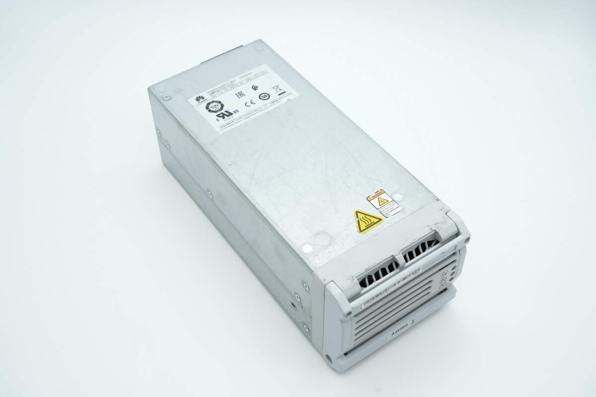
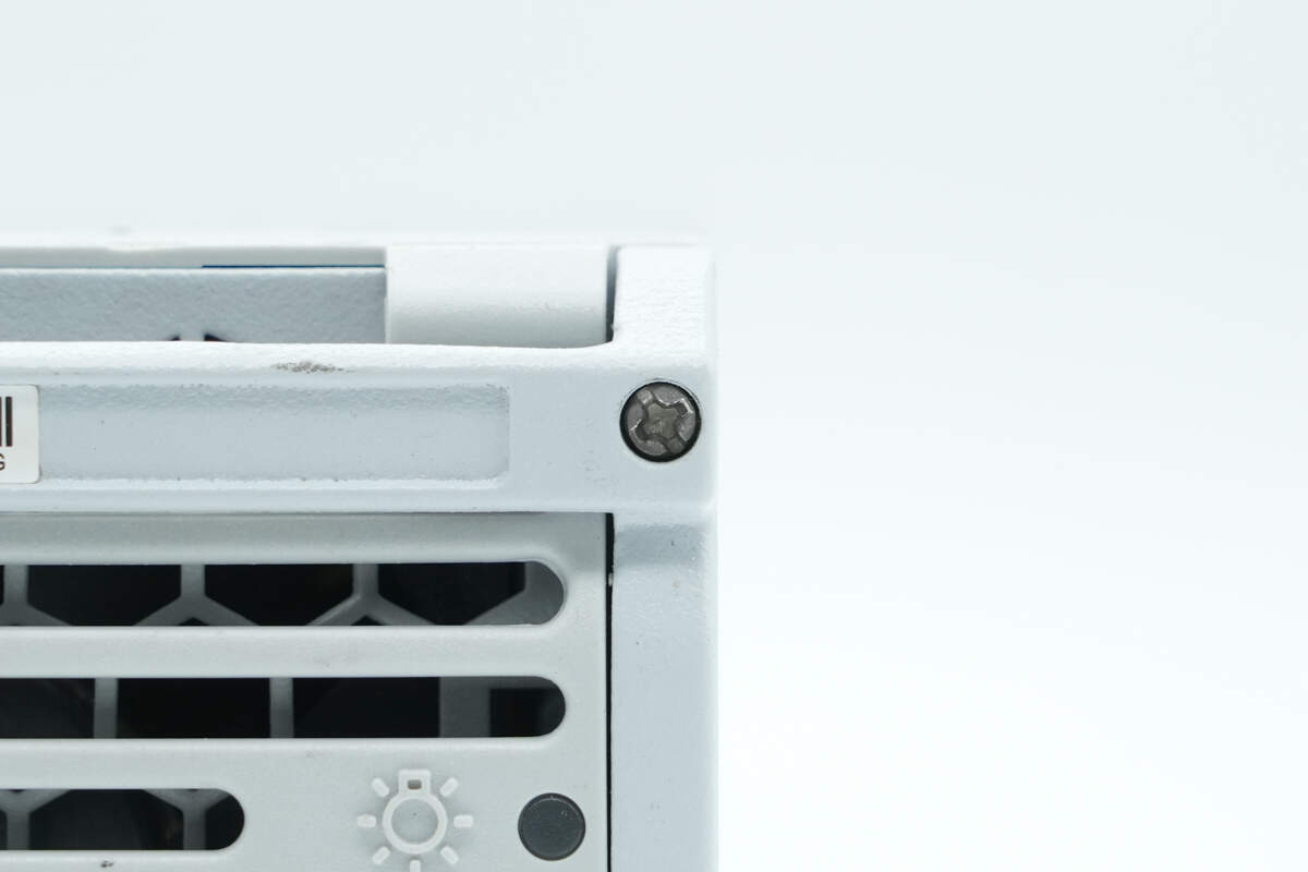
The front end of the metal casing is equipped with mounting clips.
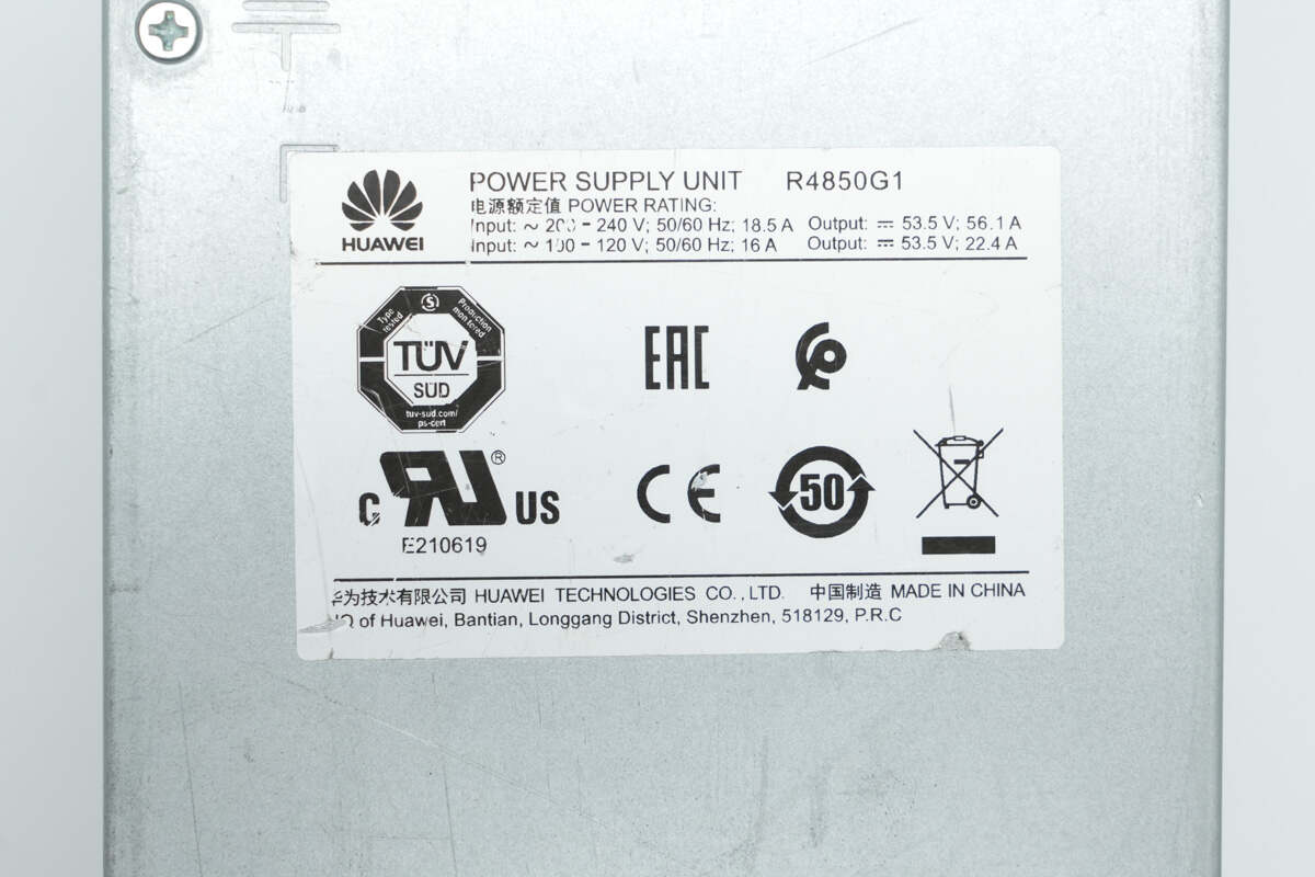
Model: R4850G1
Power Ratings:
Input: \~200-240V; 50/60Hz; 18.5A
Output: 53.5V; 56.1A
Input: \~100-120V; 50/60Hz; 16A
Output: 53.5V; 22.4A
It is certified by TUV, EAC, CP, UL, and CE.
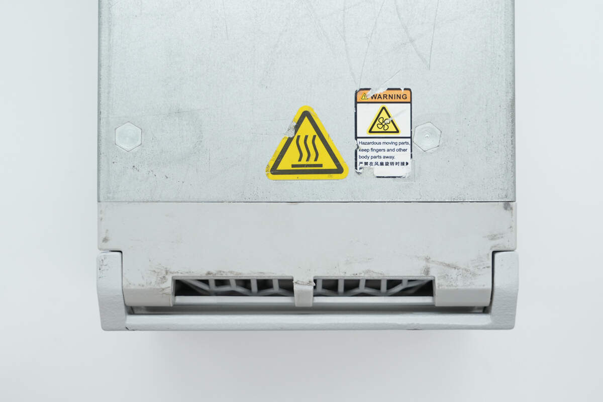
There are warning labels on the top.
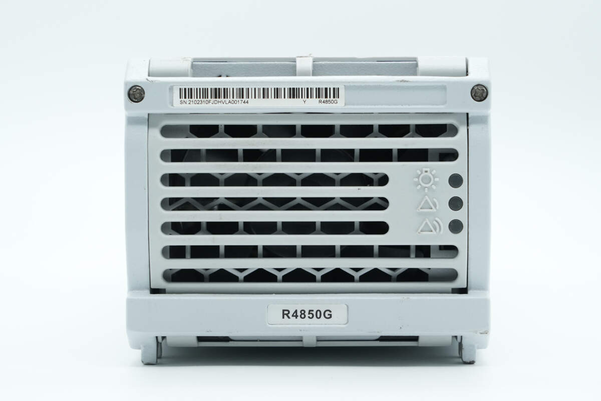
The mounting clips are secured with screws. Inside, there is a cooling fan, and indicator lights are located on the right side.
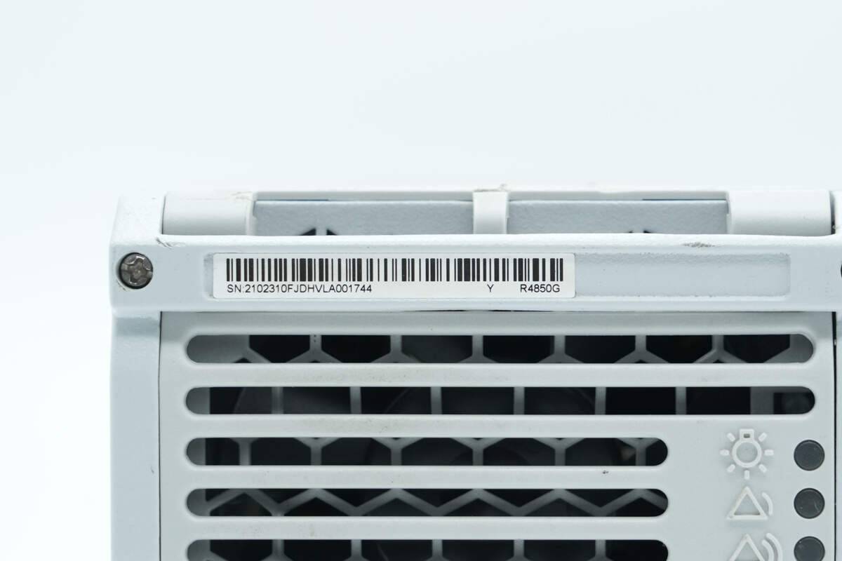
A serial number sticker is attached to the handle.
The handle is secured with screws.
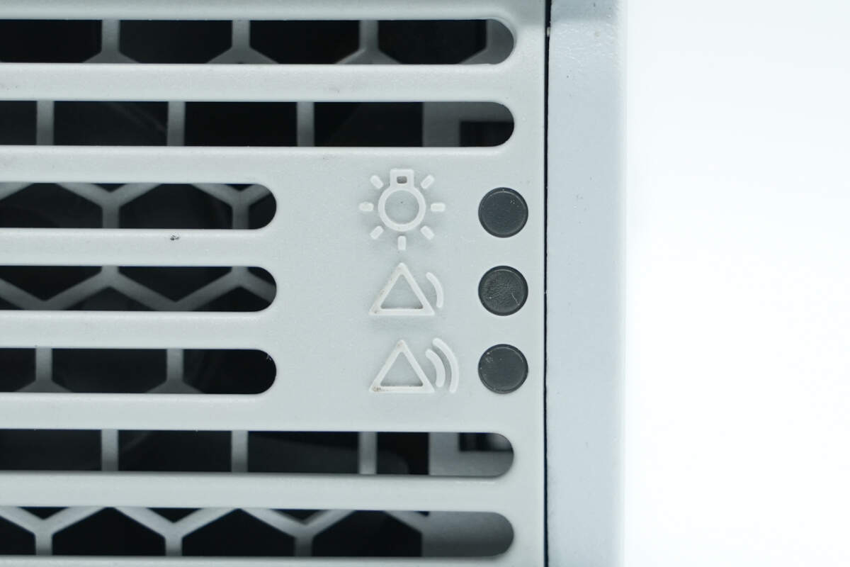
Close-up of the power indicator light, alarm indicator light, and fault indicator light.
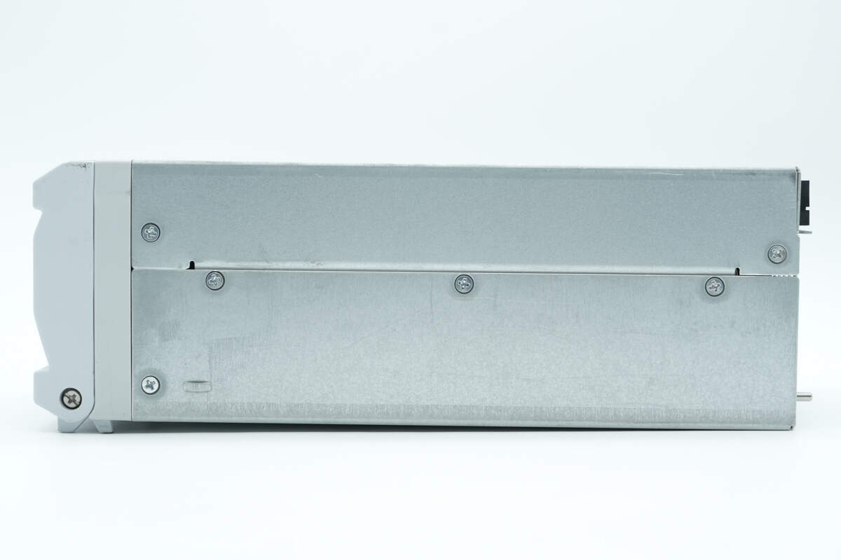
There are fixing screws on the side.
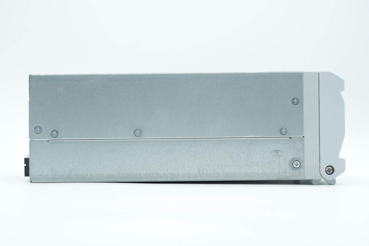
The other side is also equipped with fixing screws.
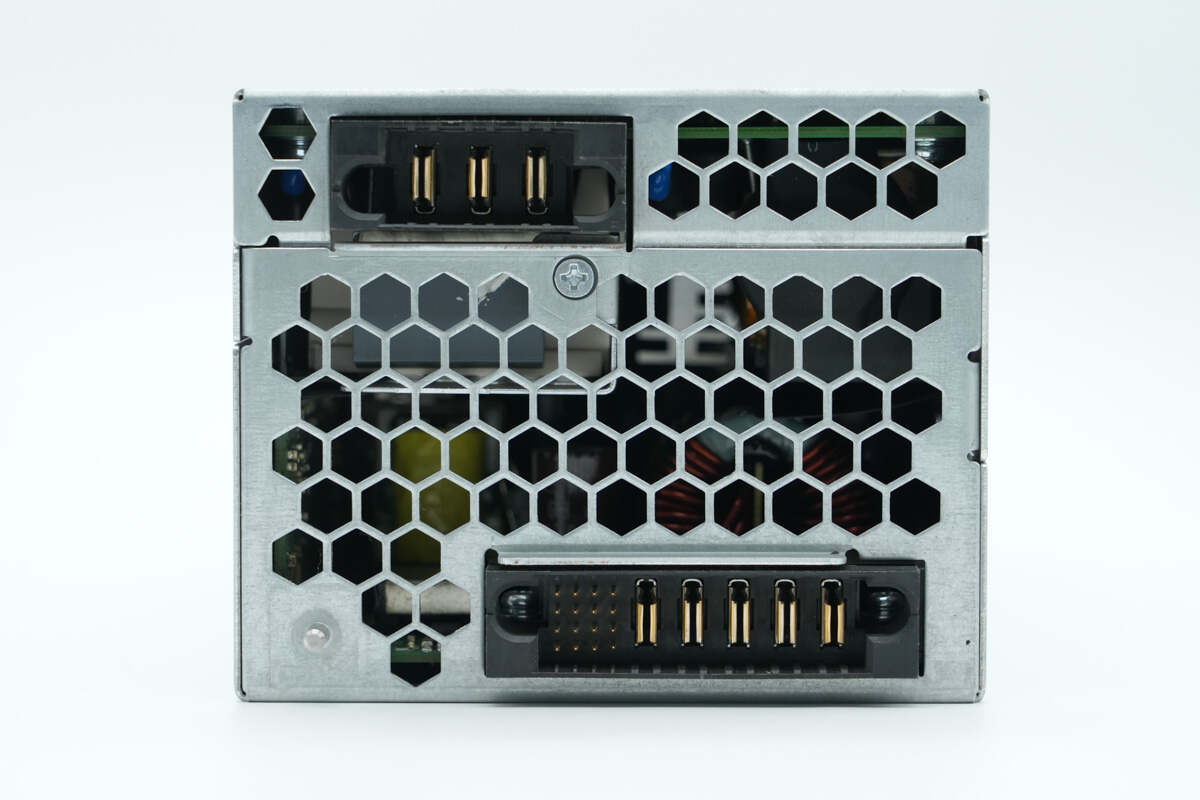
The rear side features ventilation openings and sockets.
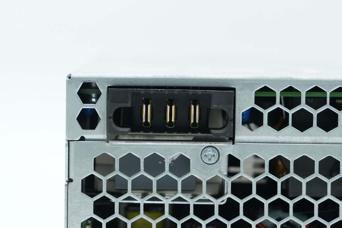
Close-up of the AC input socket.
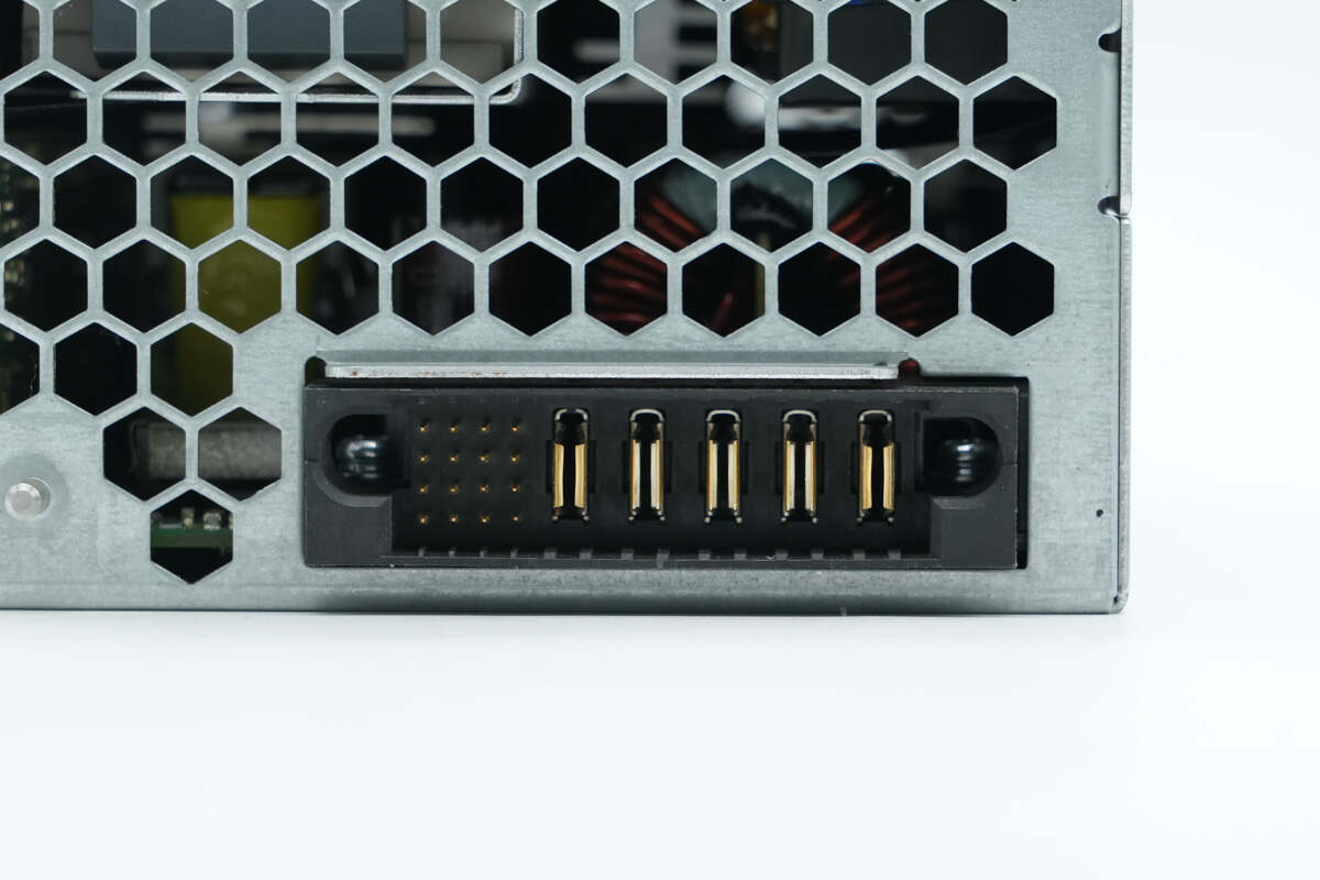
Close-up of the communication interface and DC output socket.
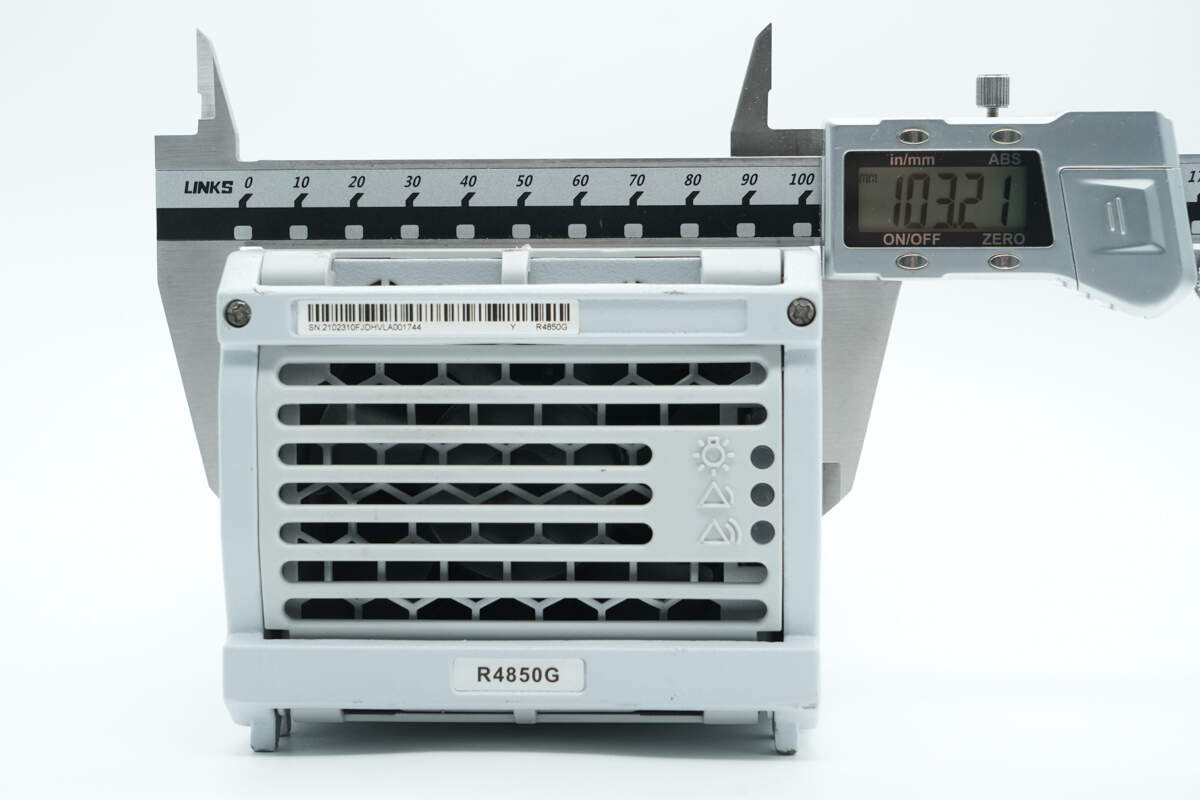
The width is about 103.2 mm (4.063 inches).
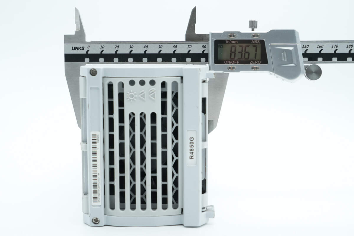
The thickness is about 83.7 mm (3.3 inches).
The length of the module is about 242 mm (9.53 inches).
That's how big it is in the hand.
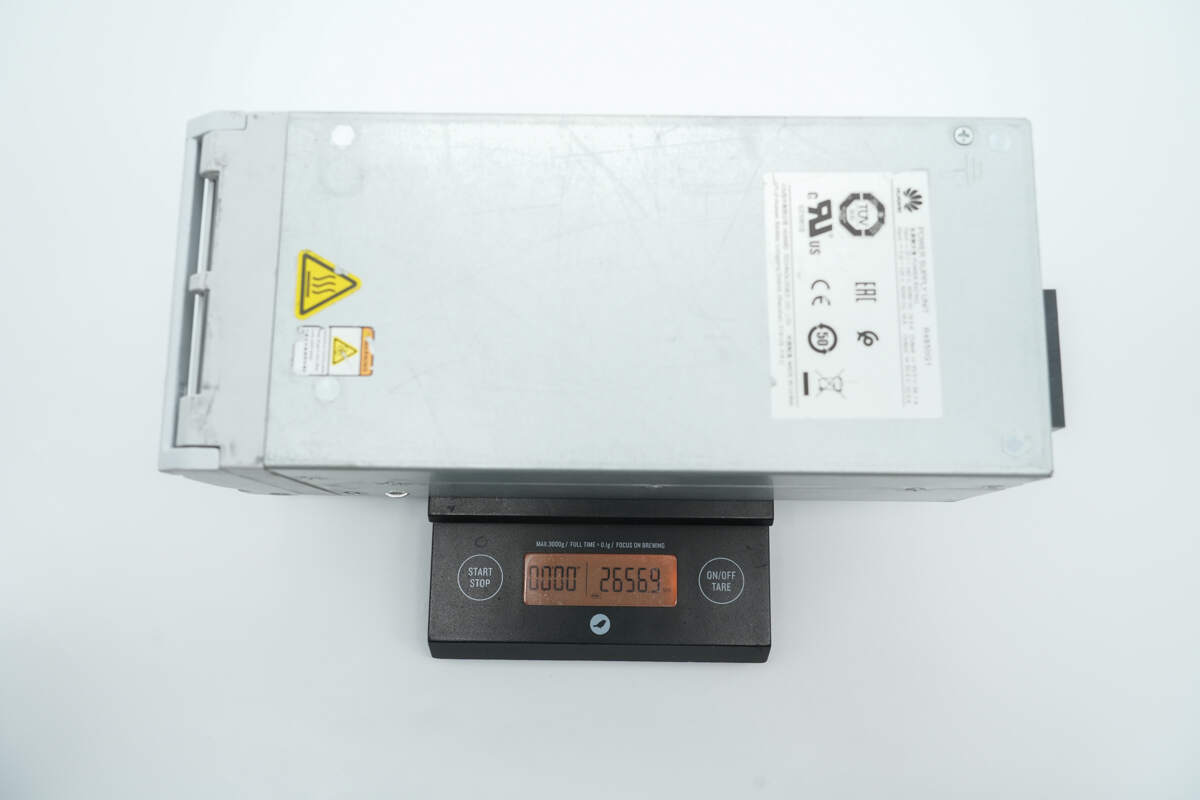
The weight is about 2656 g (5.86 lb).
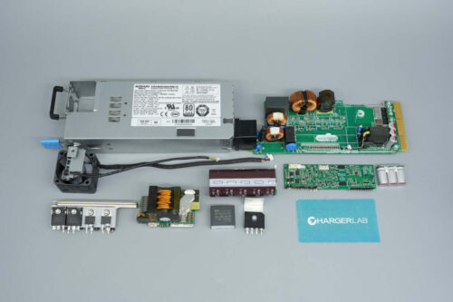
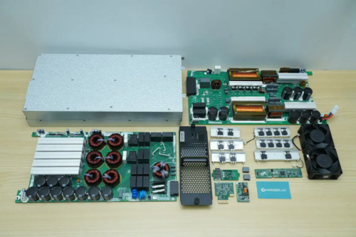
Teardown
Next, let's take it apart to see its internal components and structure.
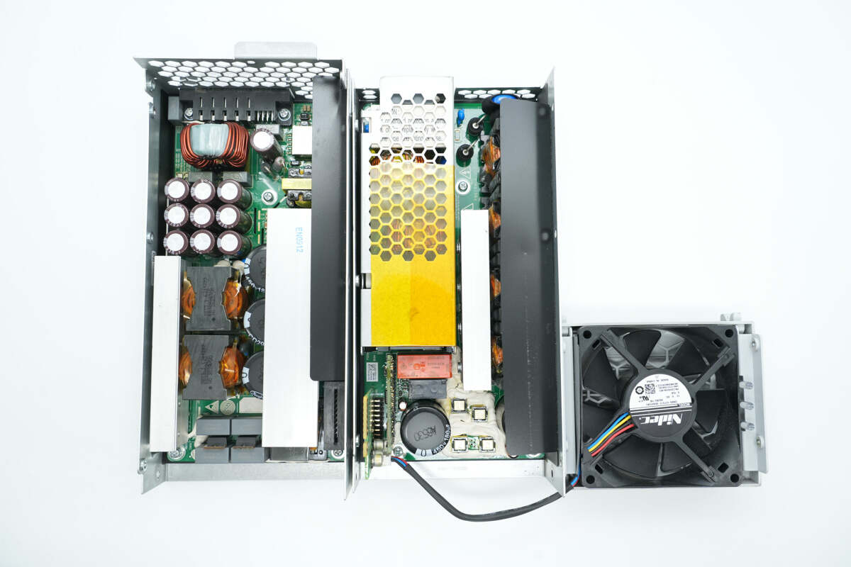
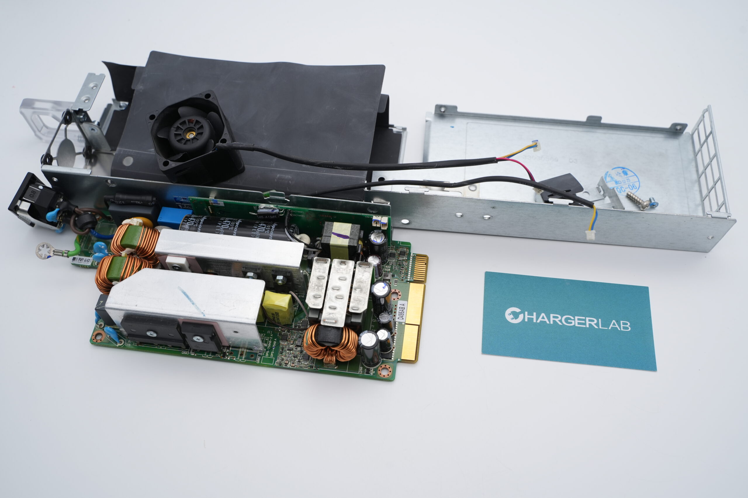
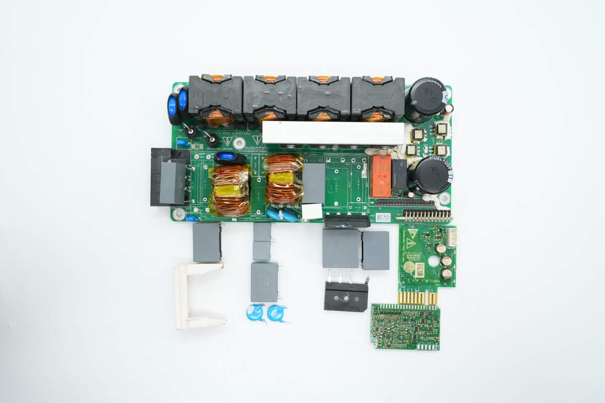
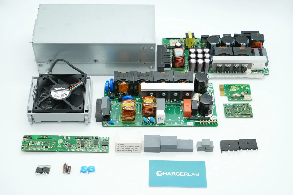
Unscrew the screws and open the casing; both parts of the enclosure have PCBs inside.
The cooling fan is connected via a plug connector.
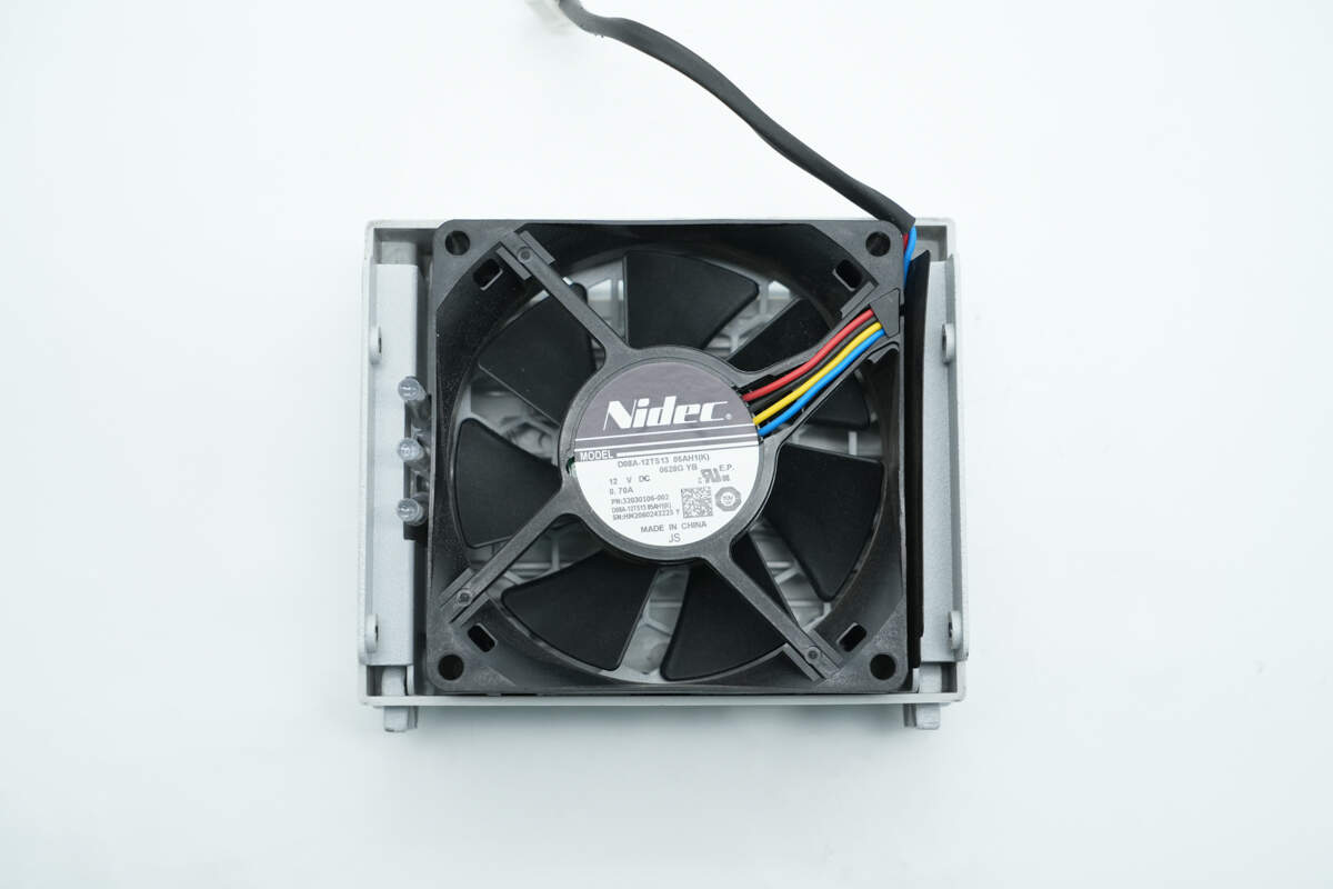
The cooling fan is from NIDEC, model D08A-12TS13, with specifications of 12V and 0.7A.
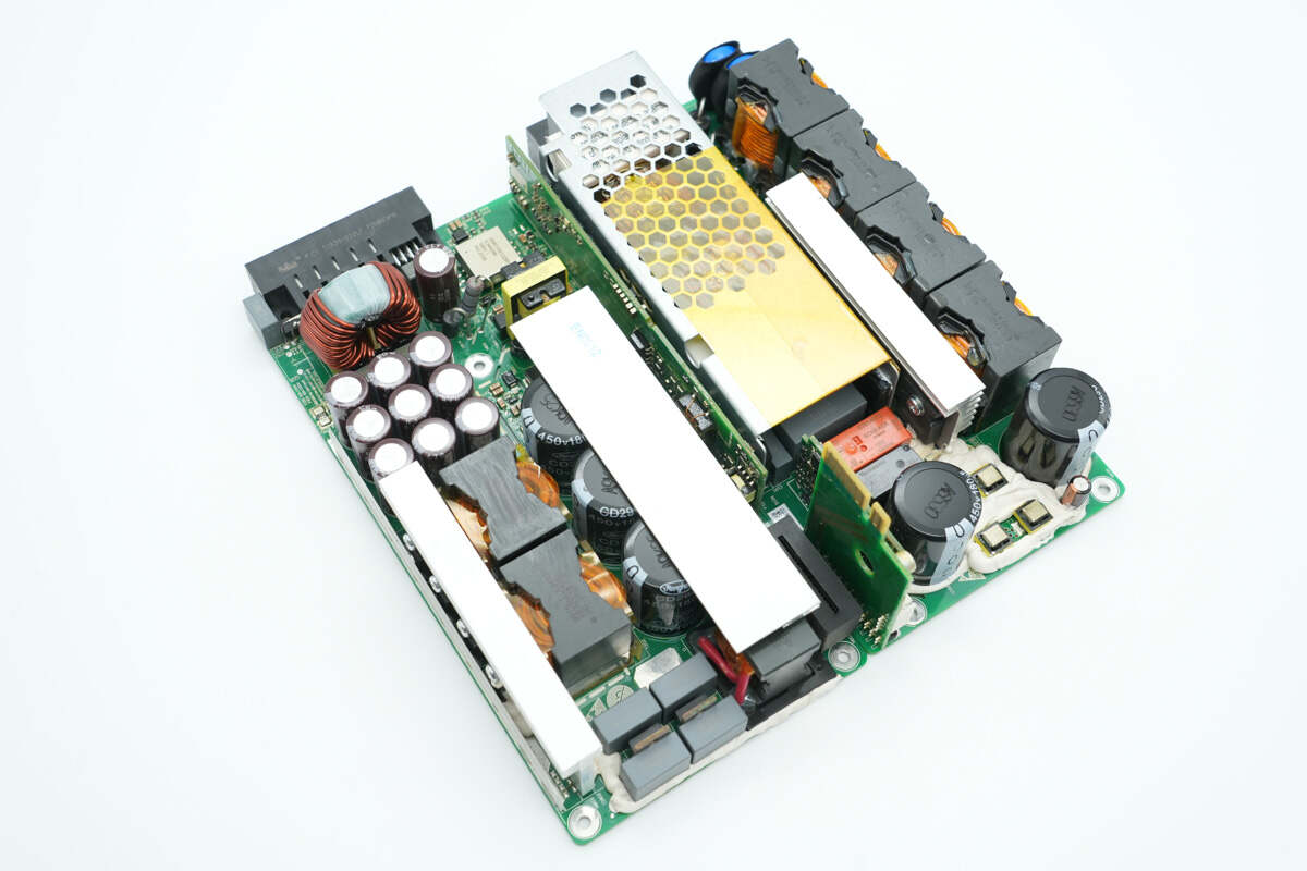
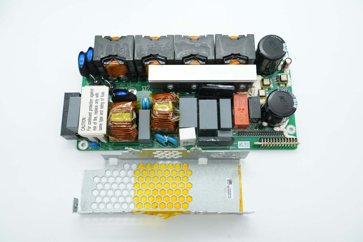
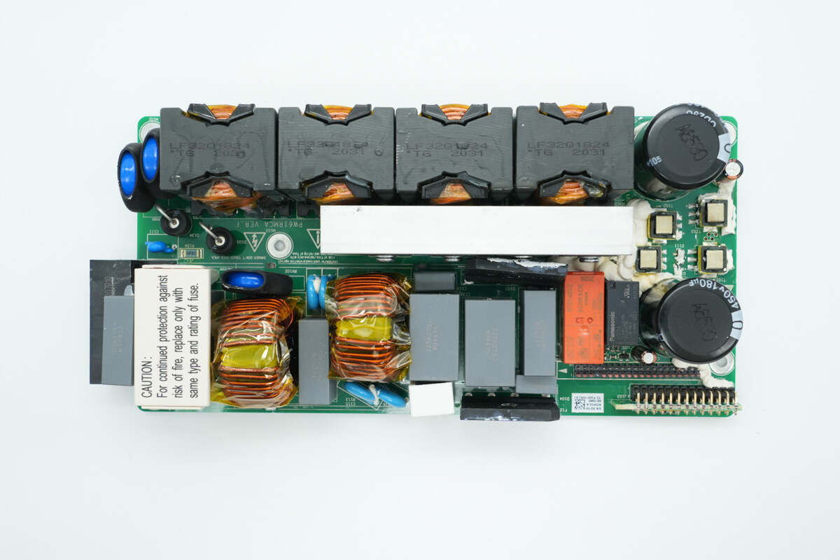
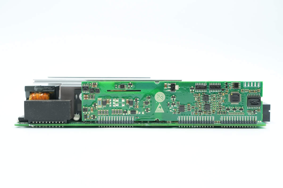
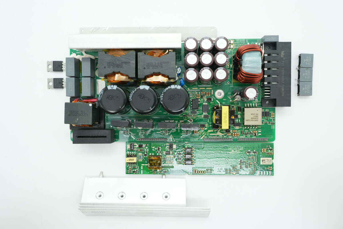
The PCBA module is taken out from the enclosure. The right side is the PFC module, and the left side is the LLC module, connected by a small PCB and plug connectors.
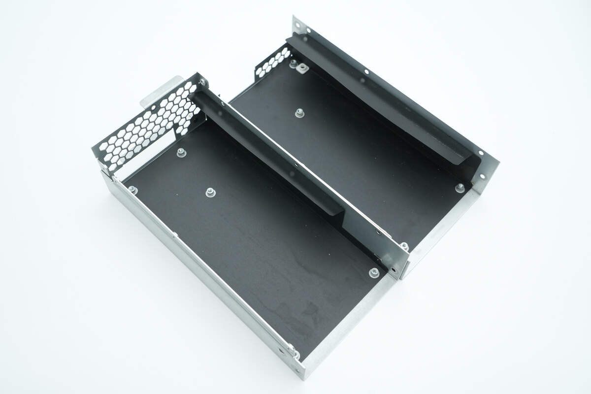
Inside the enclosure, there are insulating Mylar sheets.
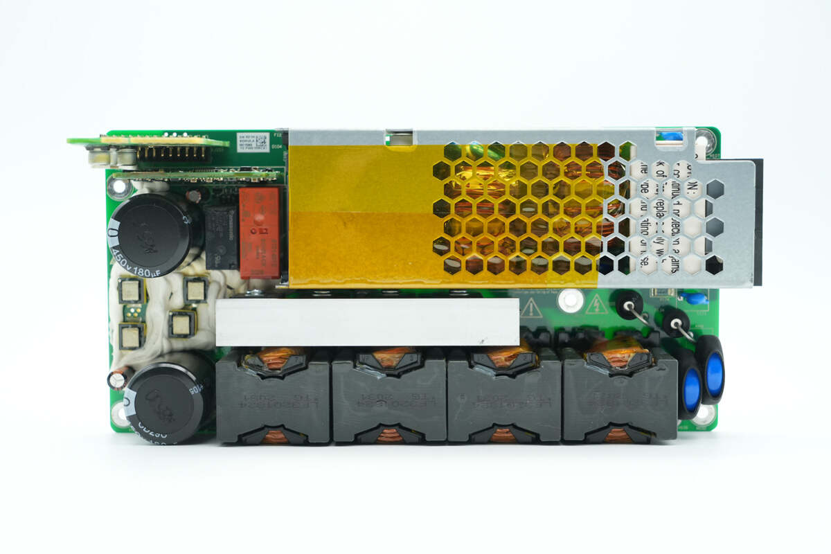
At the top front of the PFC module, there is a shield cover for cooling the bridge rectifiers, with safety X2 capacitors and common mode chokes inside. Below are the PFC MOSFETs, followed by the PFC inductors. High-voltage filter capacitors are located on the left side. In the top left corner, there is a control PCB and a connection PCB. In the bottom right corner, there are gas discharge tubes and varistors.
On the back side, there are two half-bridge drivers.
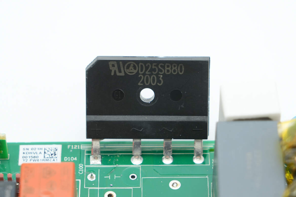
On the side of the heatsink, there are soldering tabs, and the bridge rectifiers are secured to the heatsink with screws.
After removing the shield cover, below are common mode chokes and safety X2 capacitors, among other components. The cover also serves to dissipate heat from the two bridge rectifiers.
Below the shield cover are fuses, common mode chokes, safety X2 capacitors, and bridge rectifiers.
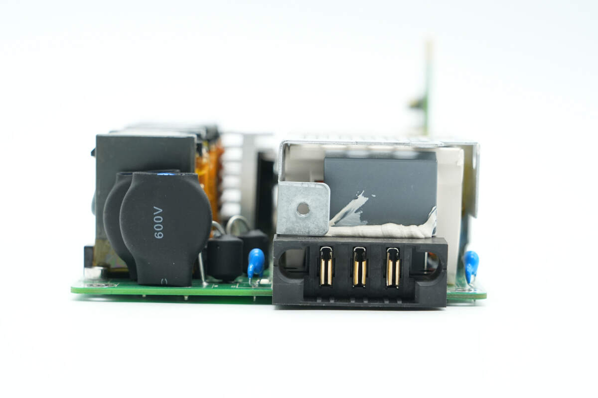
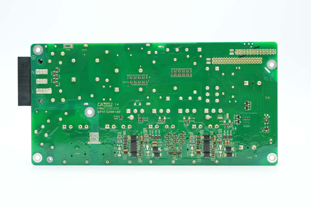
Overview of the PCBA module input side, featuring the input socket and varistors.
After removing the fuses, safety X2 capacitors, Y capacitors, and bridge rectifiers, the control PCB and connection PCB are visible on the right side.
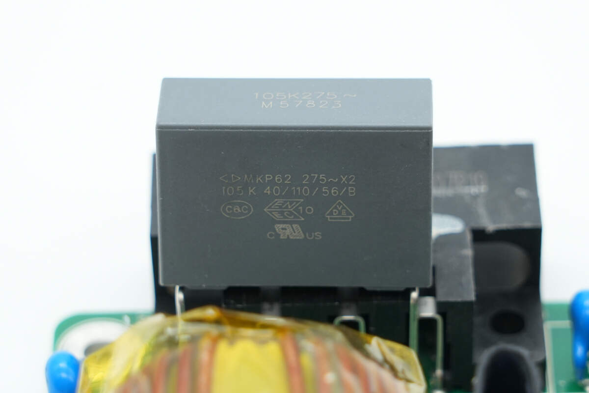
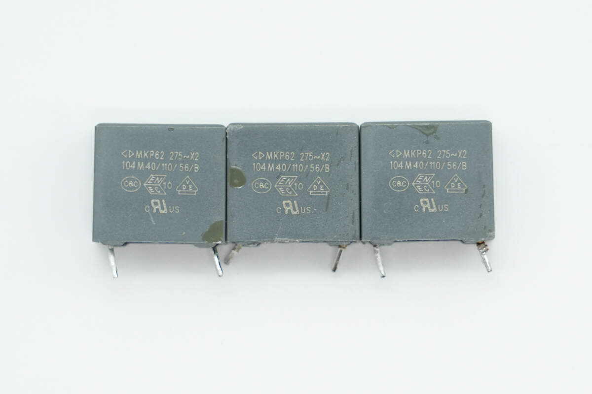
The safety X2 capacitor is from Faratronic. 1μF.
The input fuse is covered with an insulating cap.
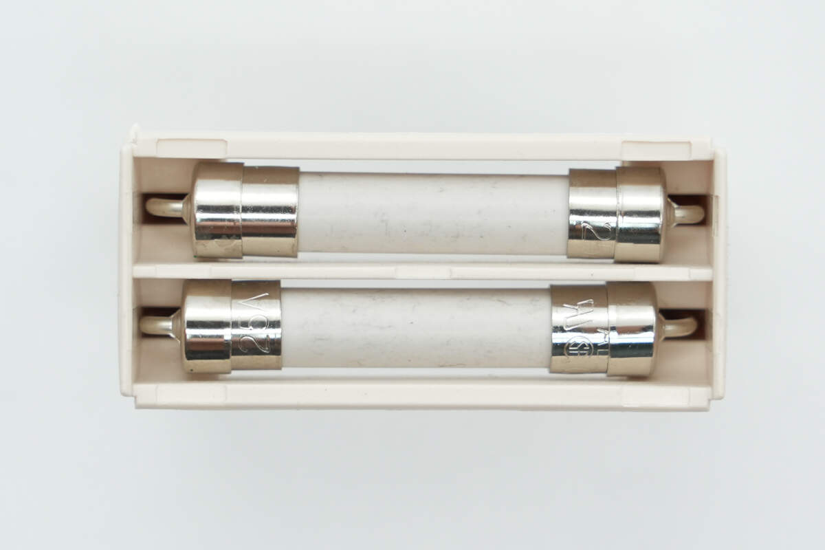
Inside, there are two fuses, each rated at 25A.
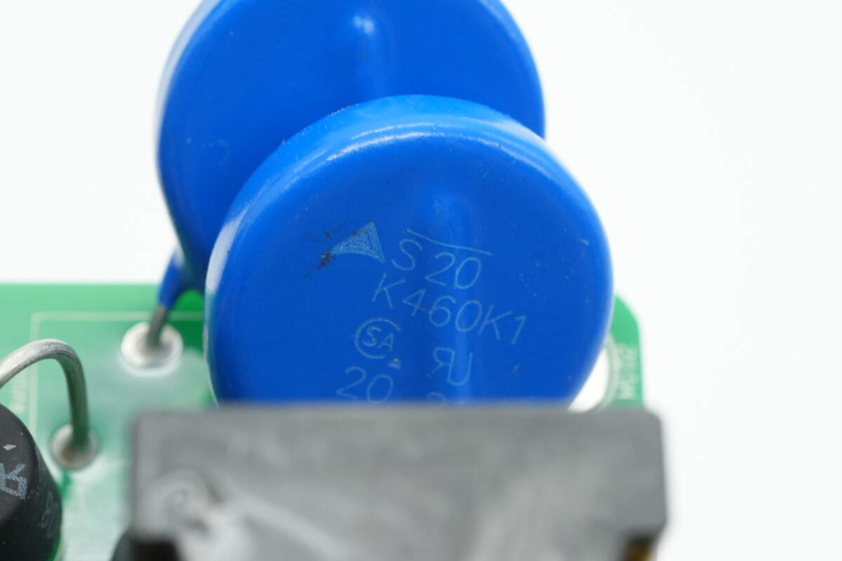
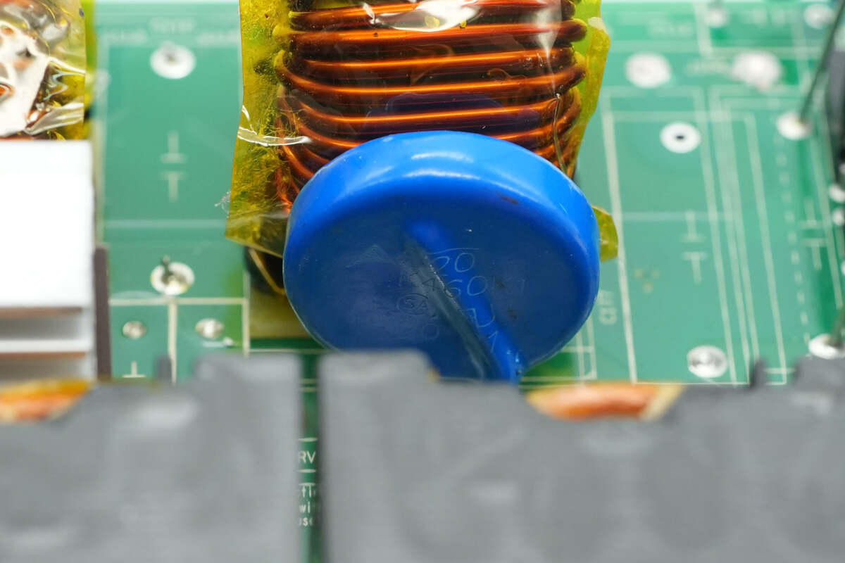
The varistor is from TDK, marked with S20K460K1.
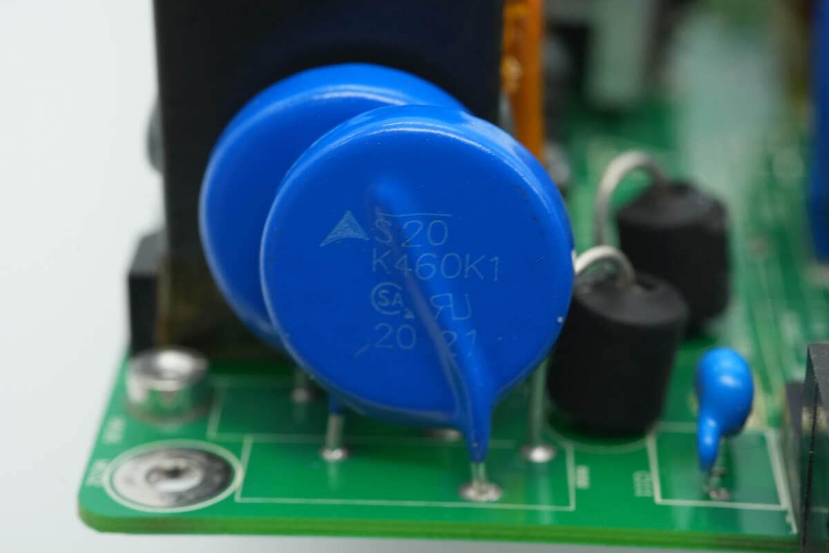
The other varistor has the same marking.
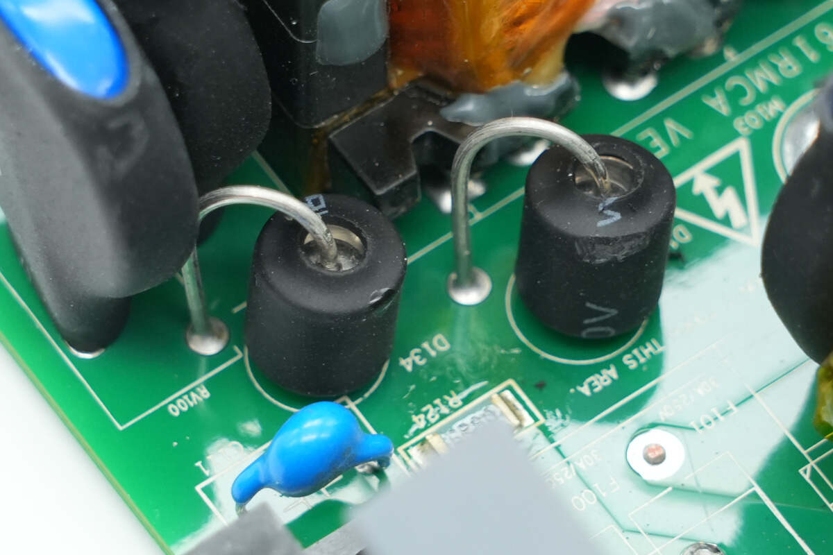
The gas discharge tube is insulated by heat-shrinkable tubing and works together with the varistor for lightning protection.
A total of three varistors are used for lightning protection.
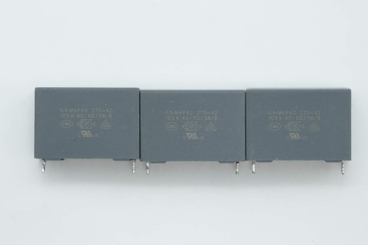
The three safety X2 capacitors are 1μF in specification.
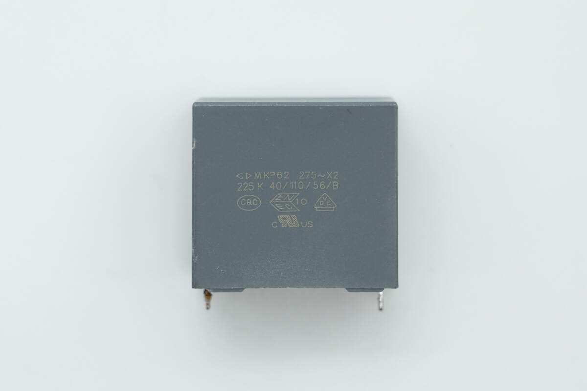
The three safety X2 capacitors are each rated at 1 μF.
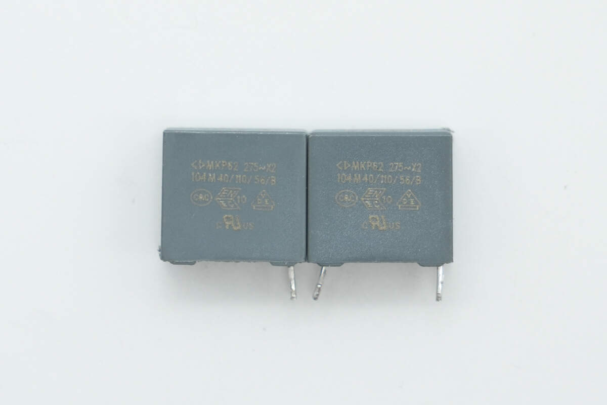
The two film capacitors are each rated at 0.1 μF.
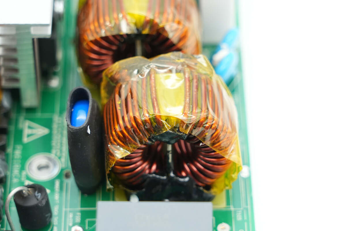
The common mode choke is wound with magnetic and insulated wires and wrapped with high-temperature insulating tape.
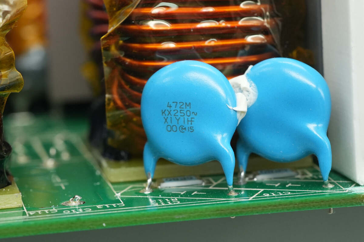
Two blue Y capacitors from MURATA are fixed together with adhesive.
The other common mode choke is also wrapped with high-temperature insulating tape.
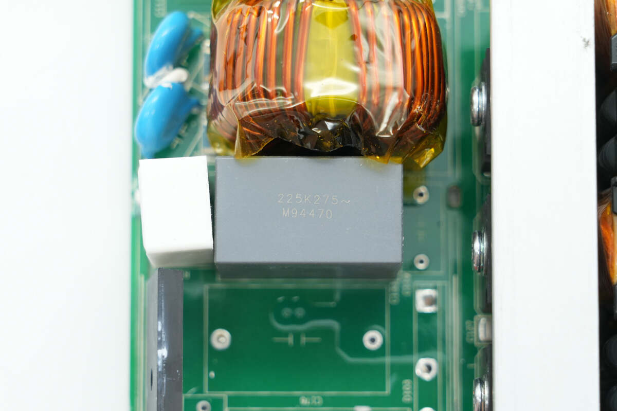
The film filter capacitor is rated at 2.2 μF.
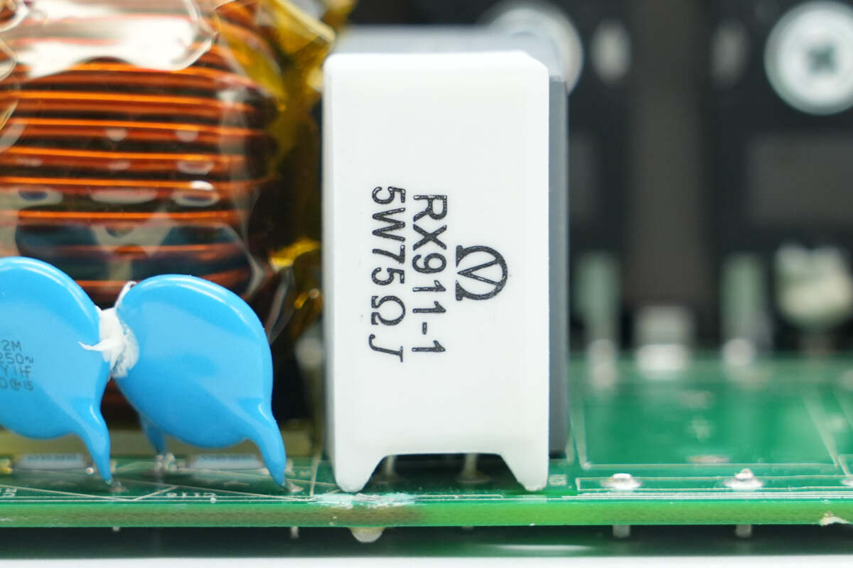
The cement resistor used for soft start is rated at 5W and 75Ω.
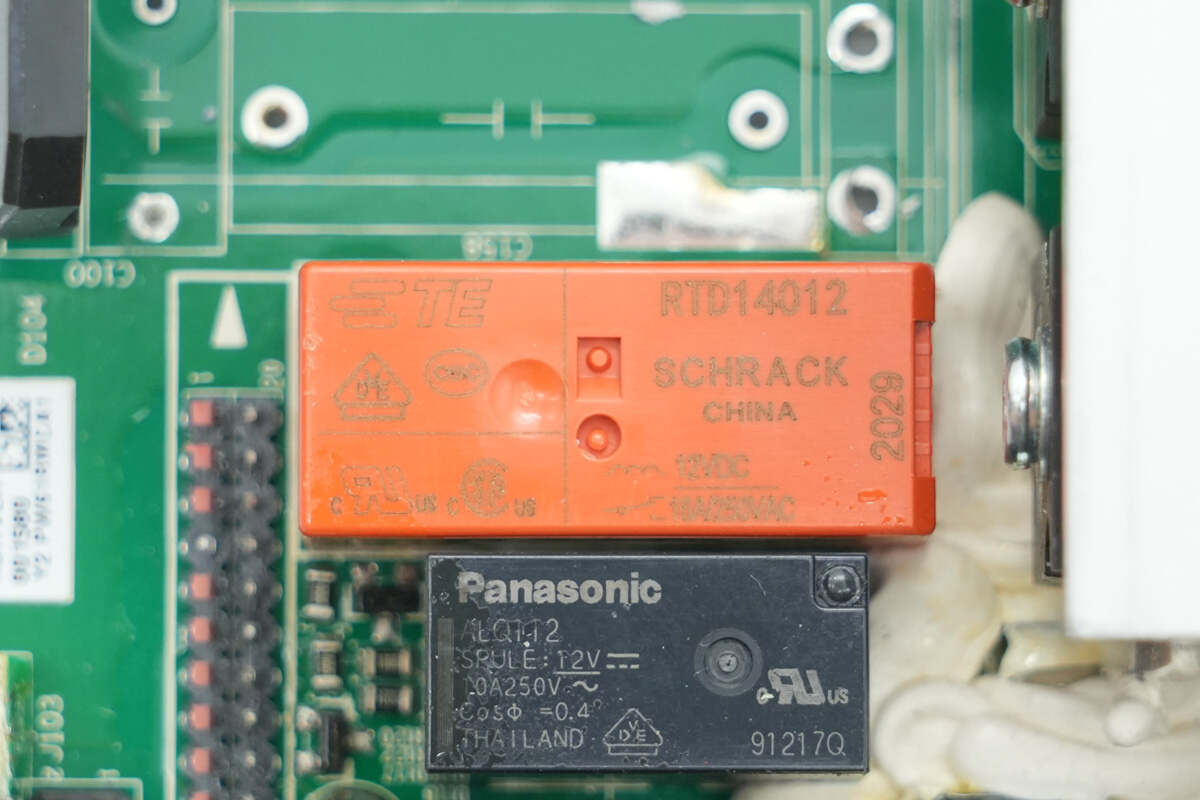
The relay is from TE, model RTD14012, featuring a single normally open contact with a contact current of 16A and a coil voltage of 12V.
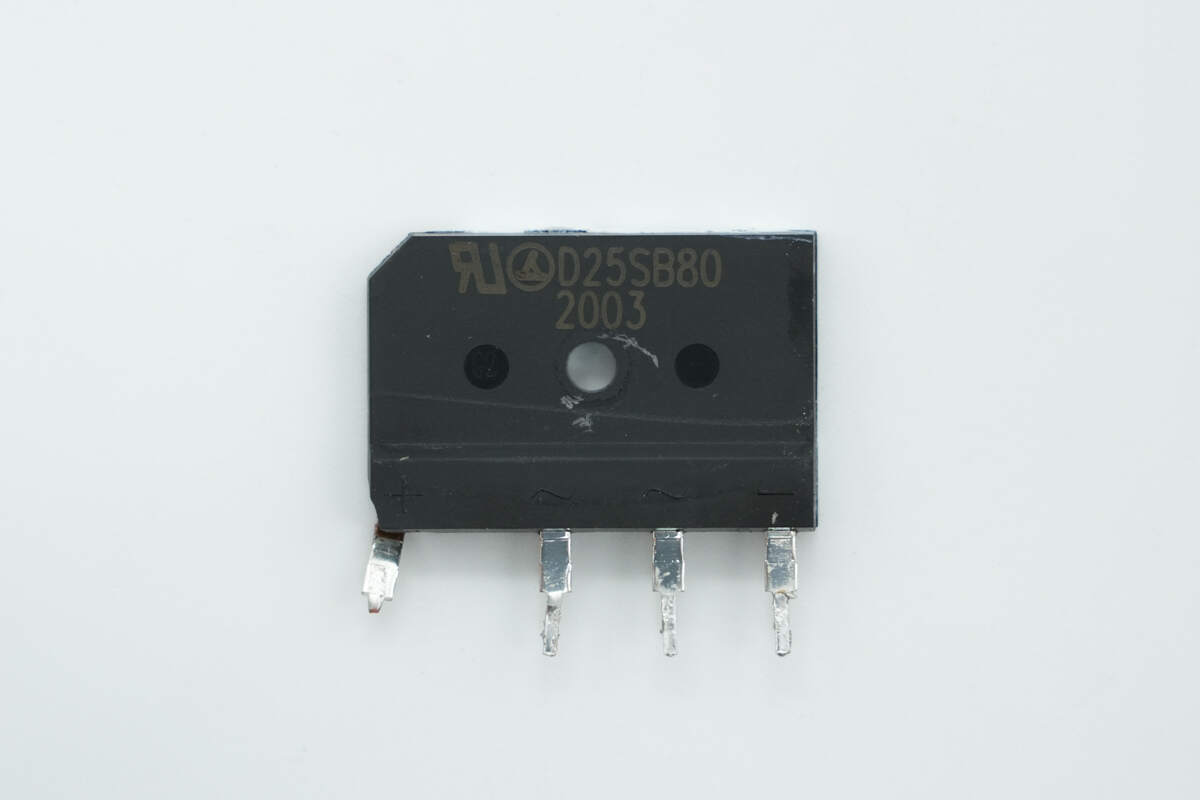
The bridge rectifier is from LRC, model D25SB80, rated at 800V and 25A, using a D5 package.
The other bridge rectifier is of the same model.
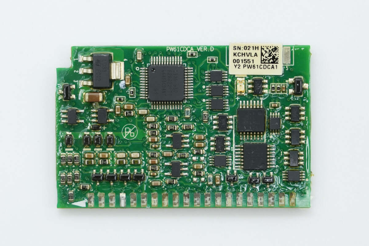
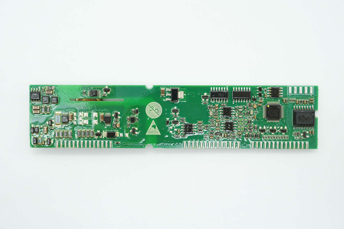
The front side of the control PCB has a PFC controller, OR gate ICs, a linear regulator, and an op-amp.
The back side features multiple chips, resistors, and capacitors.
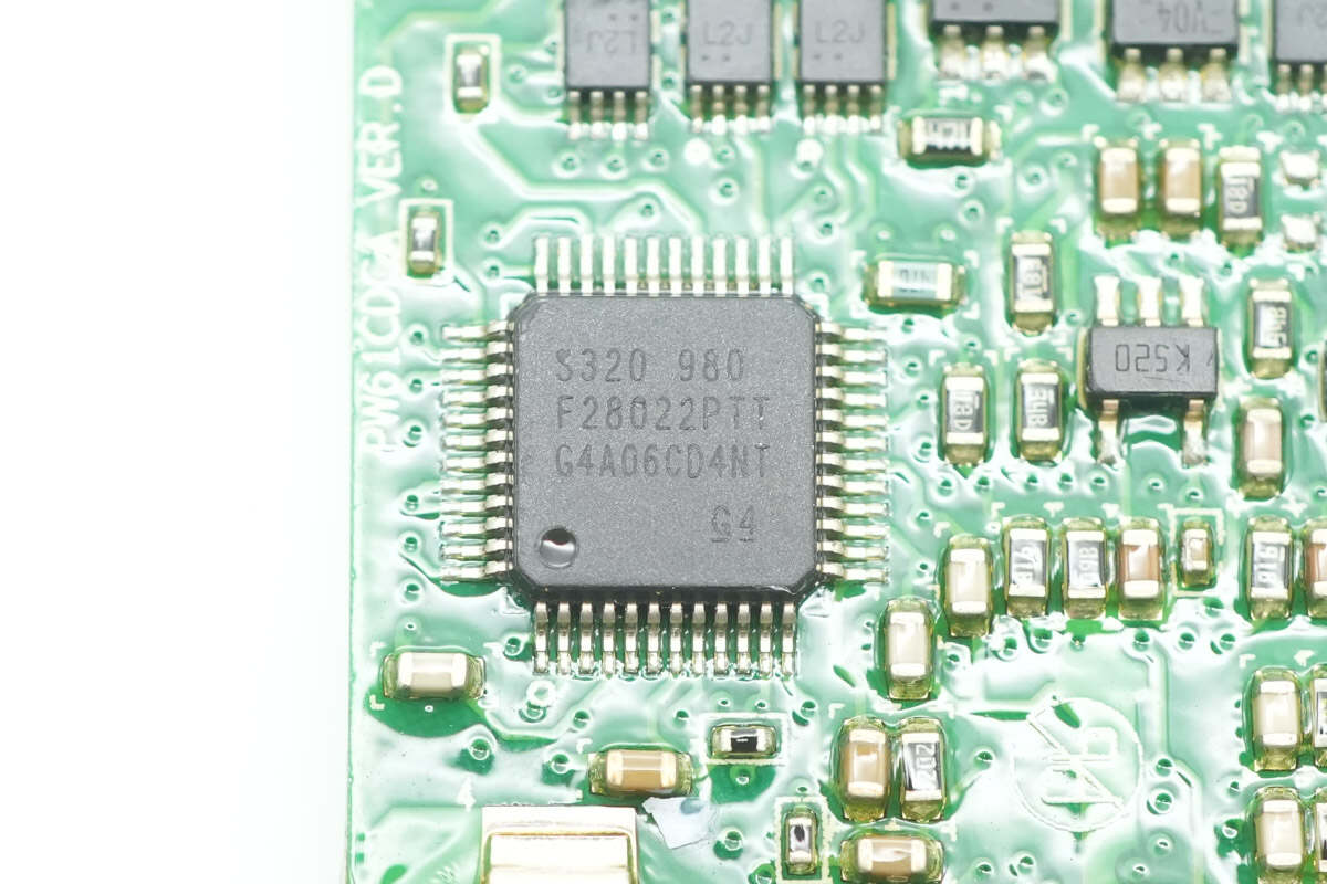
The PFC controller is from TI, model TMS320F28022. It features a built-in C2000 32-bit MCU with a main frequency of 50 MHz, 32 KB of flash, and 12 KB of SRAM. The chip supports UART, SPI, and I2C interfaces, and comes in an LQFP-48 package.
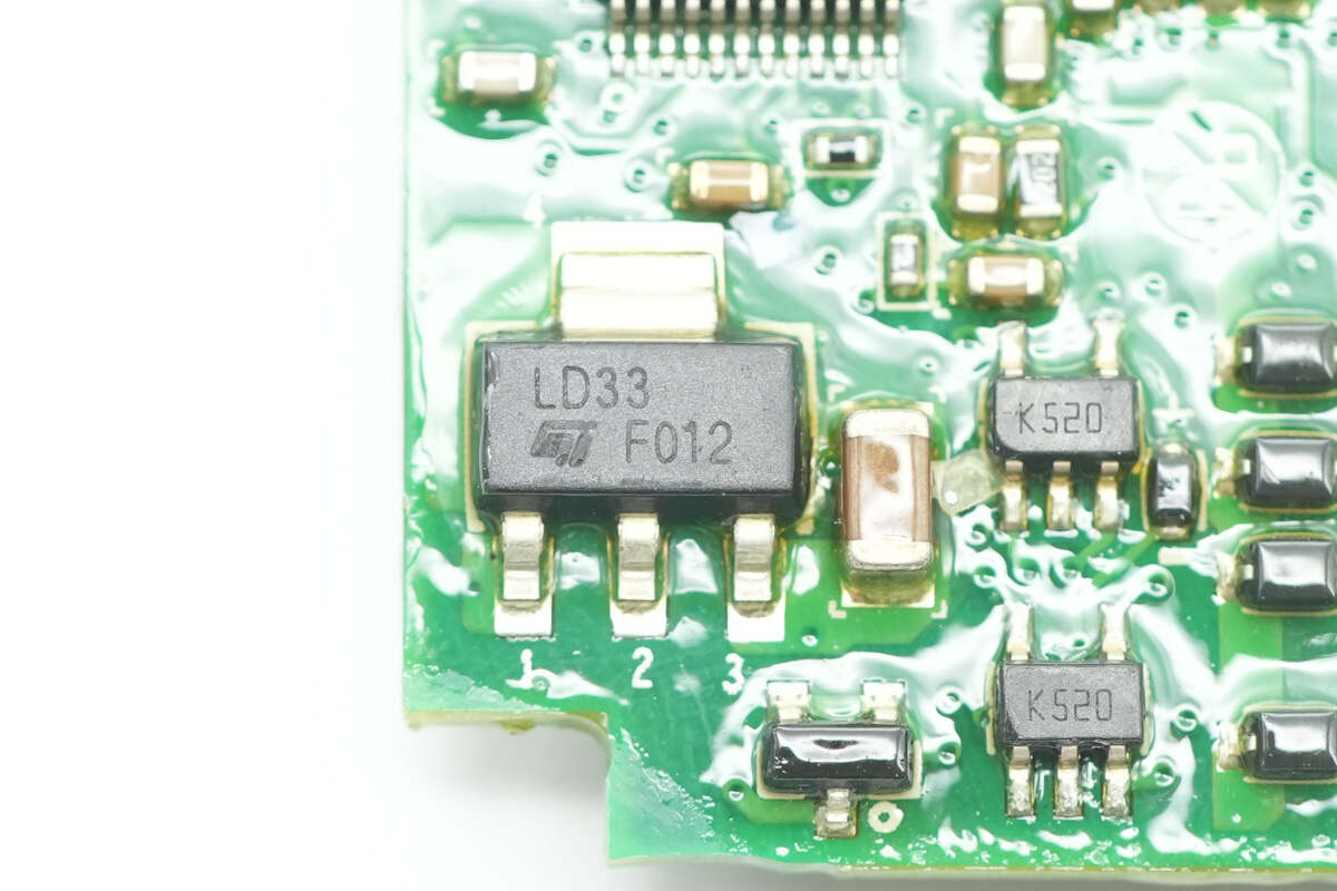
The voltage regulator is from STMicro, marked with LD33, and is used to supply power to the PFC controller. It comes in a SOT-223 package.
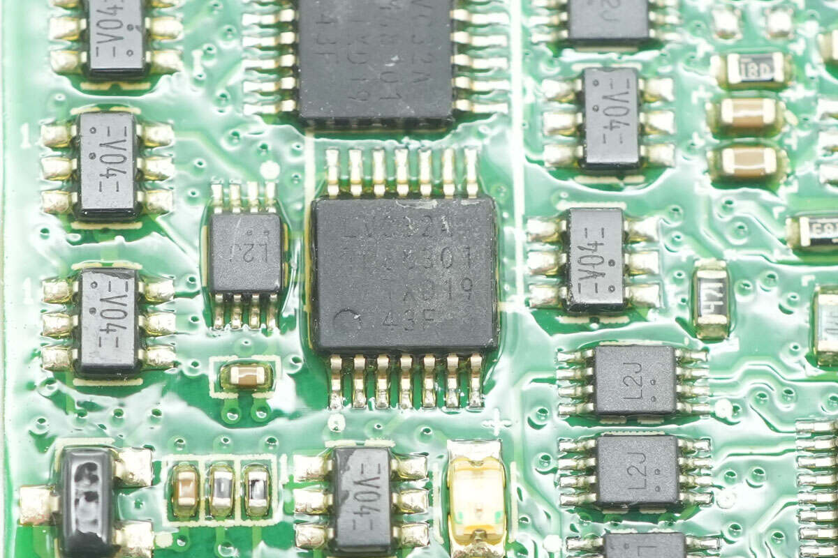
The OR gate IC is from Nexperia, model 74LVC32A. It is a quad 2-input OR gate in a TSSOP-14 package.
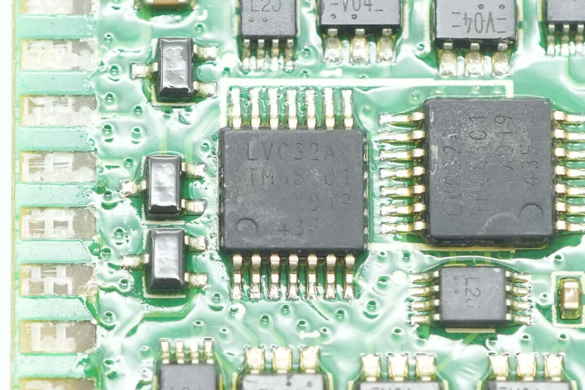
The other OR gate IC is of the same model.
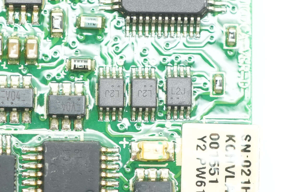
Close-up of three chips marked with L2J.
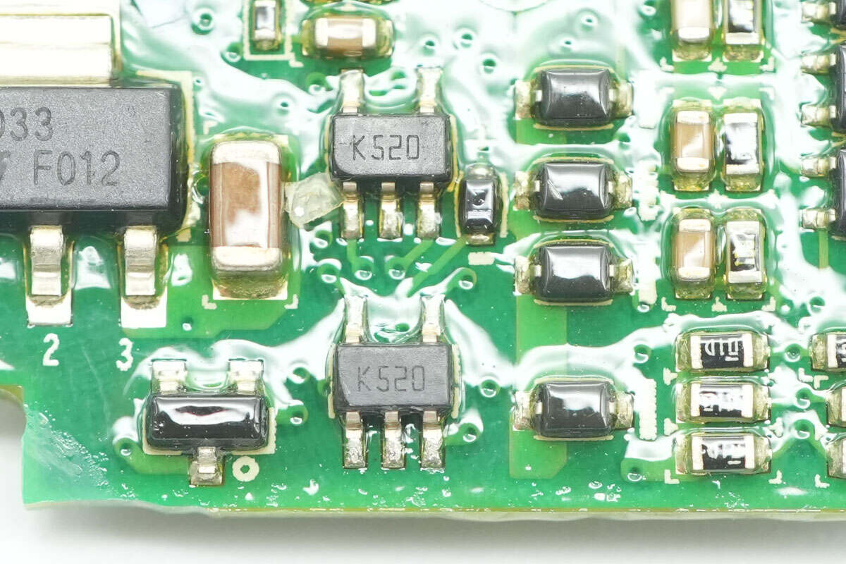
The voltage comparator is from STMicro, marked with K520, model TS3021ILT. It is a rail-to-rail input high-speed voltage comparator, supports a 1.8–5V power supply and comes in a SOT-23-5 package.
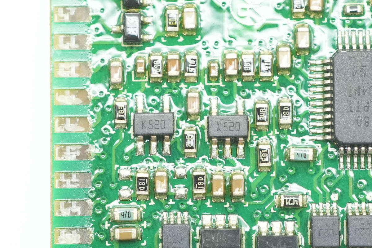
The other two voltage comparators are of the same model.
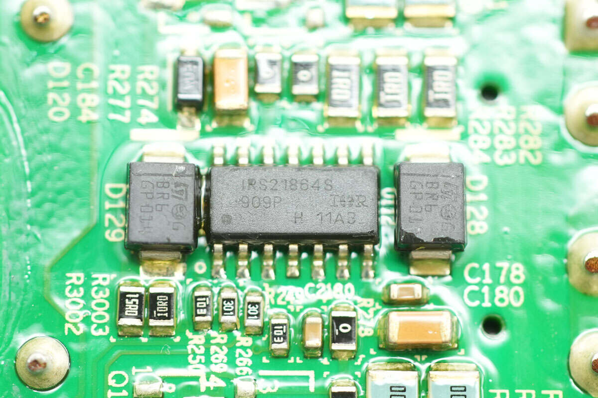
The half-bridge driver is from Infineon, model IRS21864S. The chip has a voltage rating of 600V and features 4A sourcing and 4A sinking current capabilities. It supports both IGBT and MOSFET applications and comes in a SOIC-14 package.
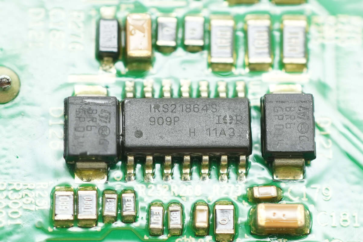
Another half-bridge driver with the same model.
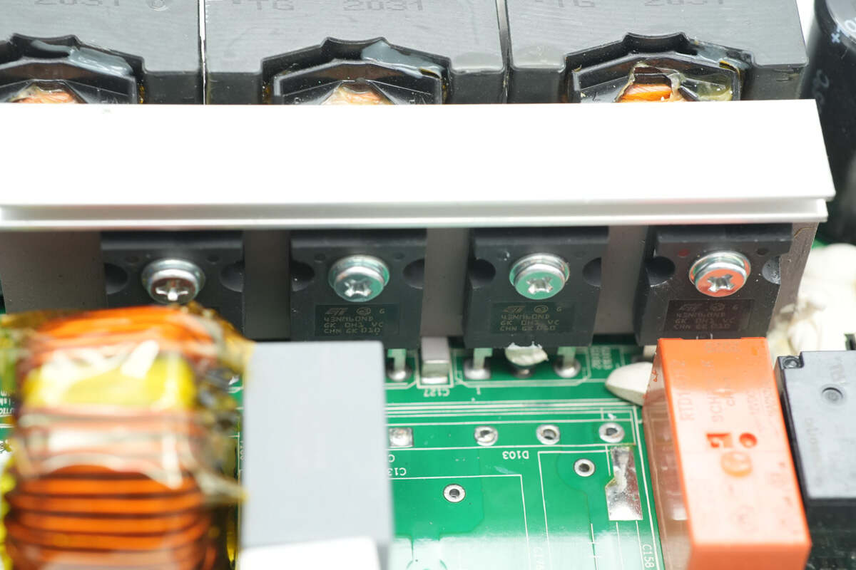
Four PFC MOSFETs are mounted on the heatsink.
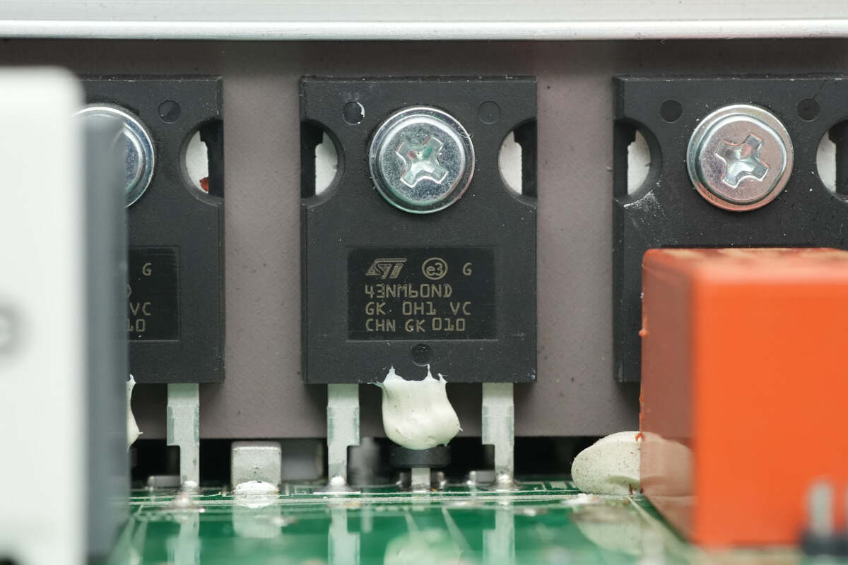
The PFC MOSFET is from STMicro, model STW43NM60ND. It is an NMOS with a voltage rating of 600V, an on-resistance of 75mΩ, and comes in a TO-247 package.
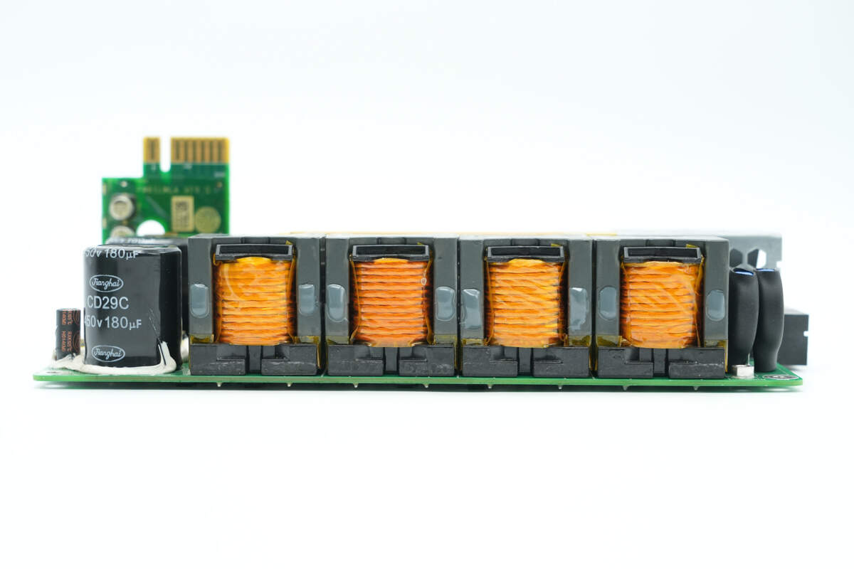
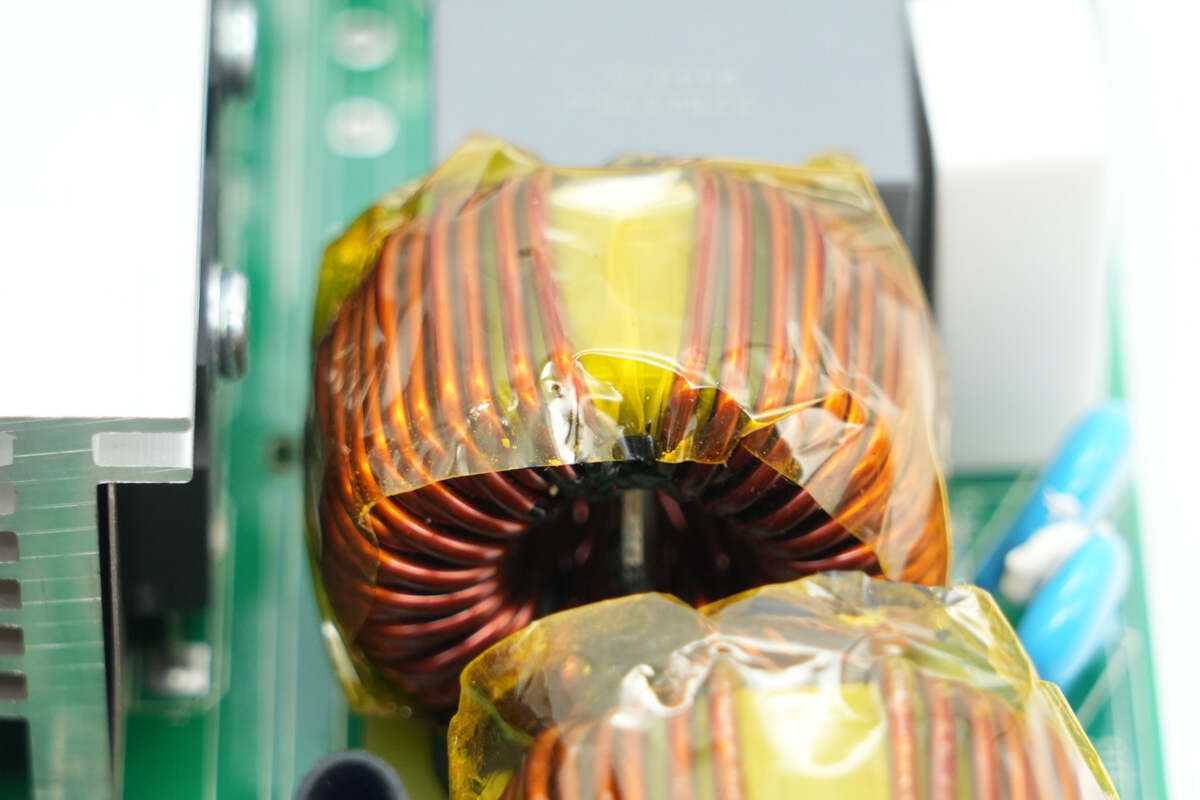
The PFC inductors are soldered on the side of the PCBA module.
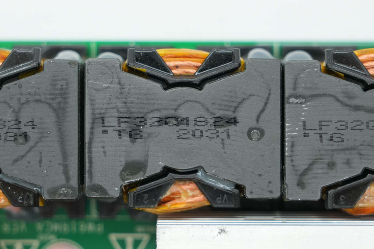
The PFC inductors are wound with Litz wire.
Close-up of four SMD current transformers.
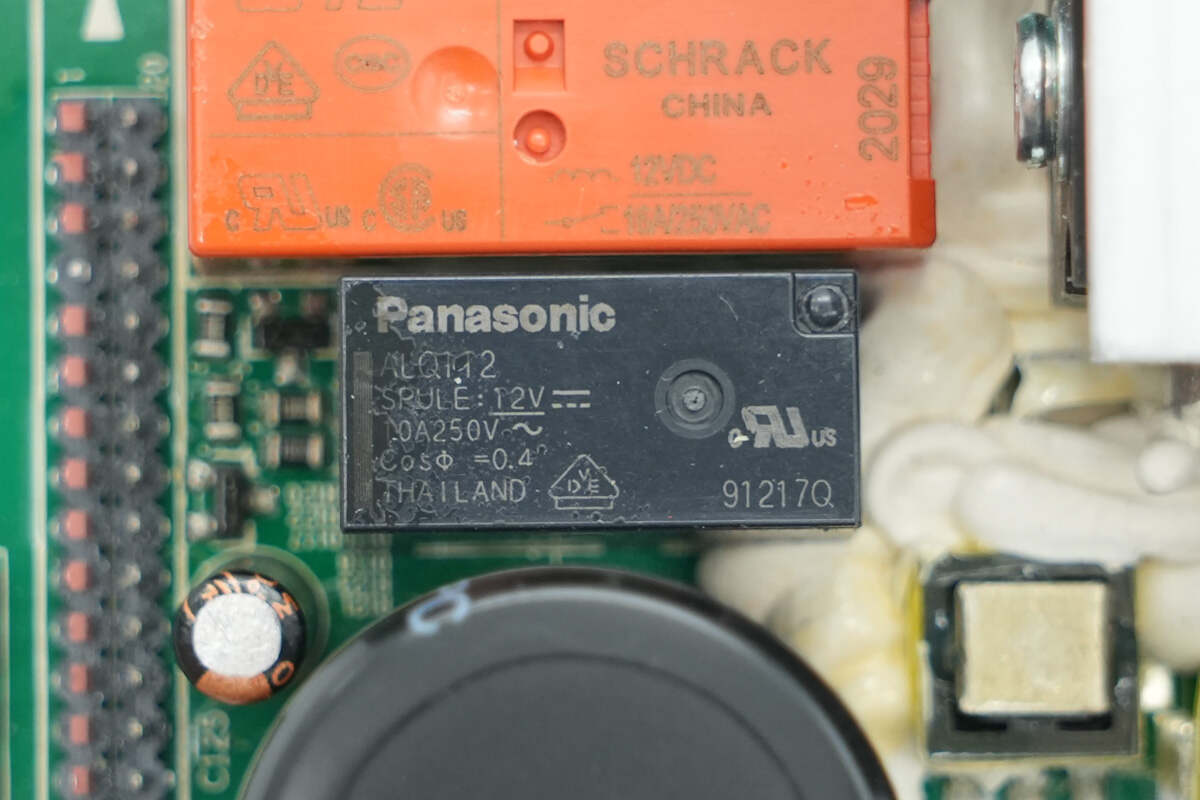
The relay is from Panasonic, model ALQ112. It features a built-in single-pole double-throw (SPDT) contact, with a contact rating of 10A and a coil voltage of 12V.
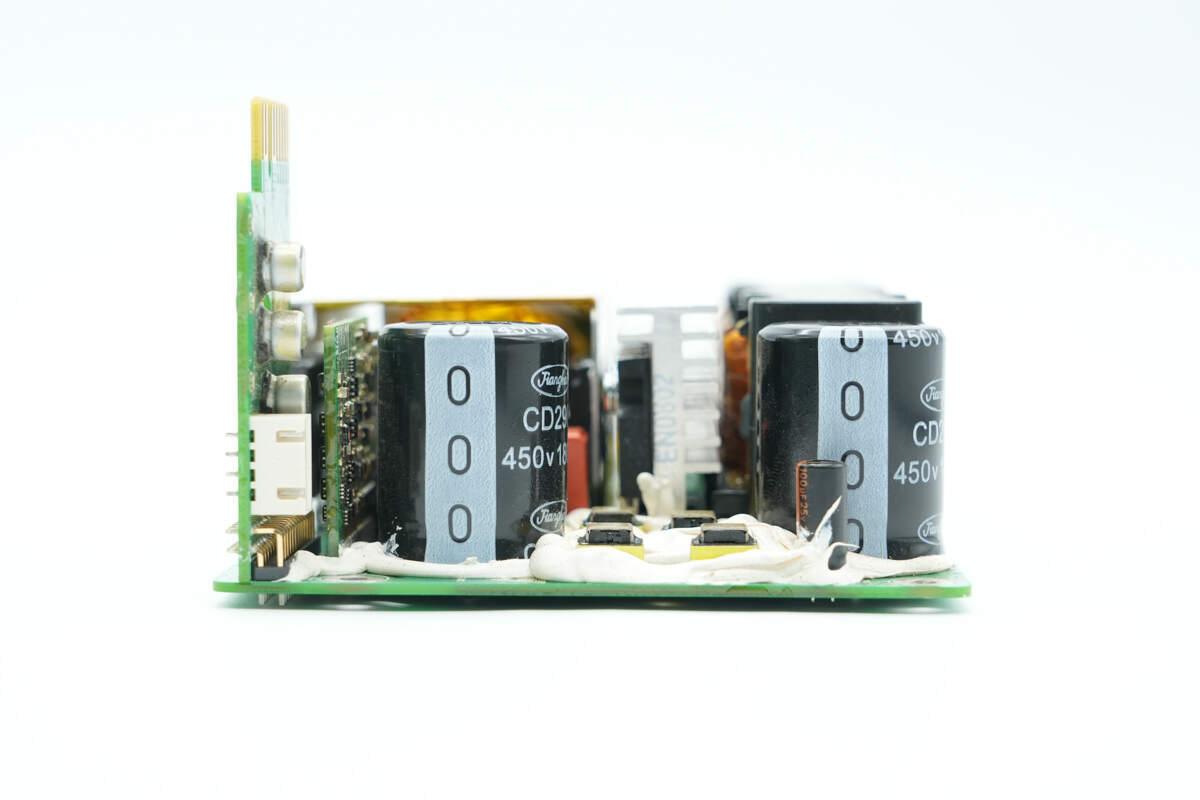
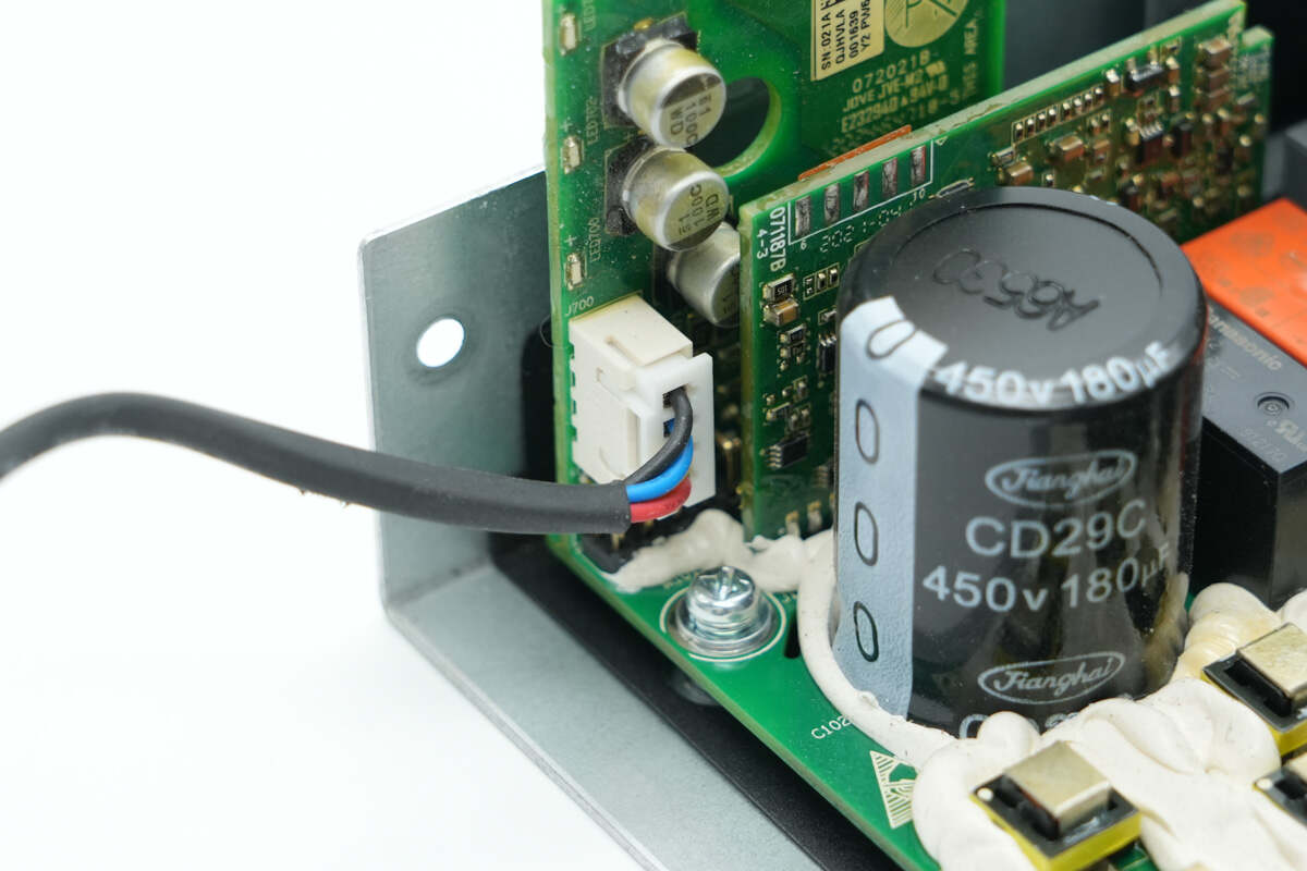
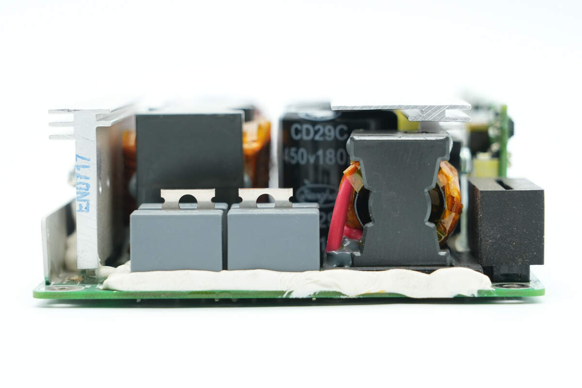
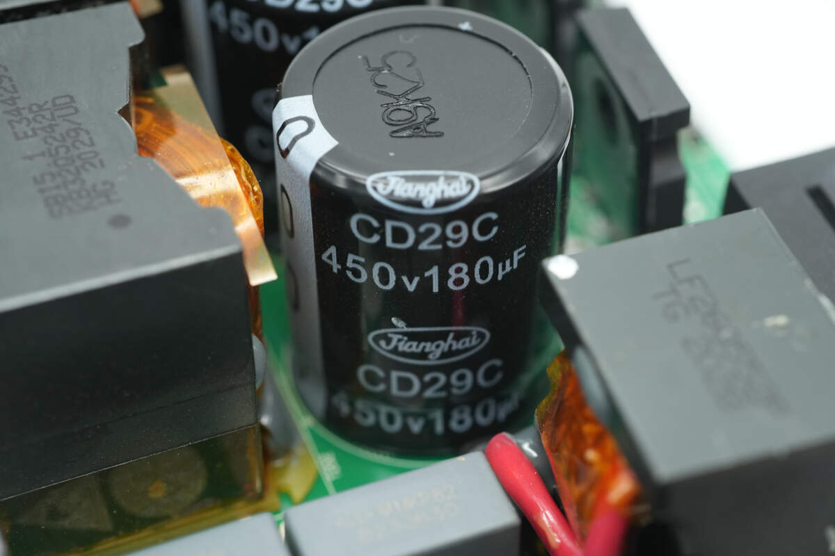
Two filter capacitors are installed at the output.
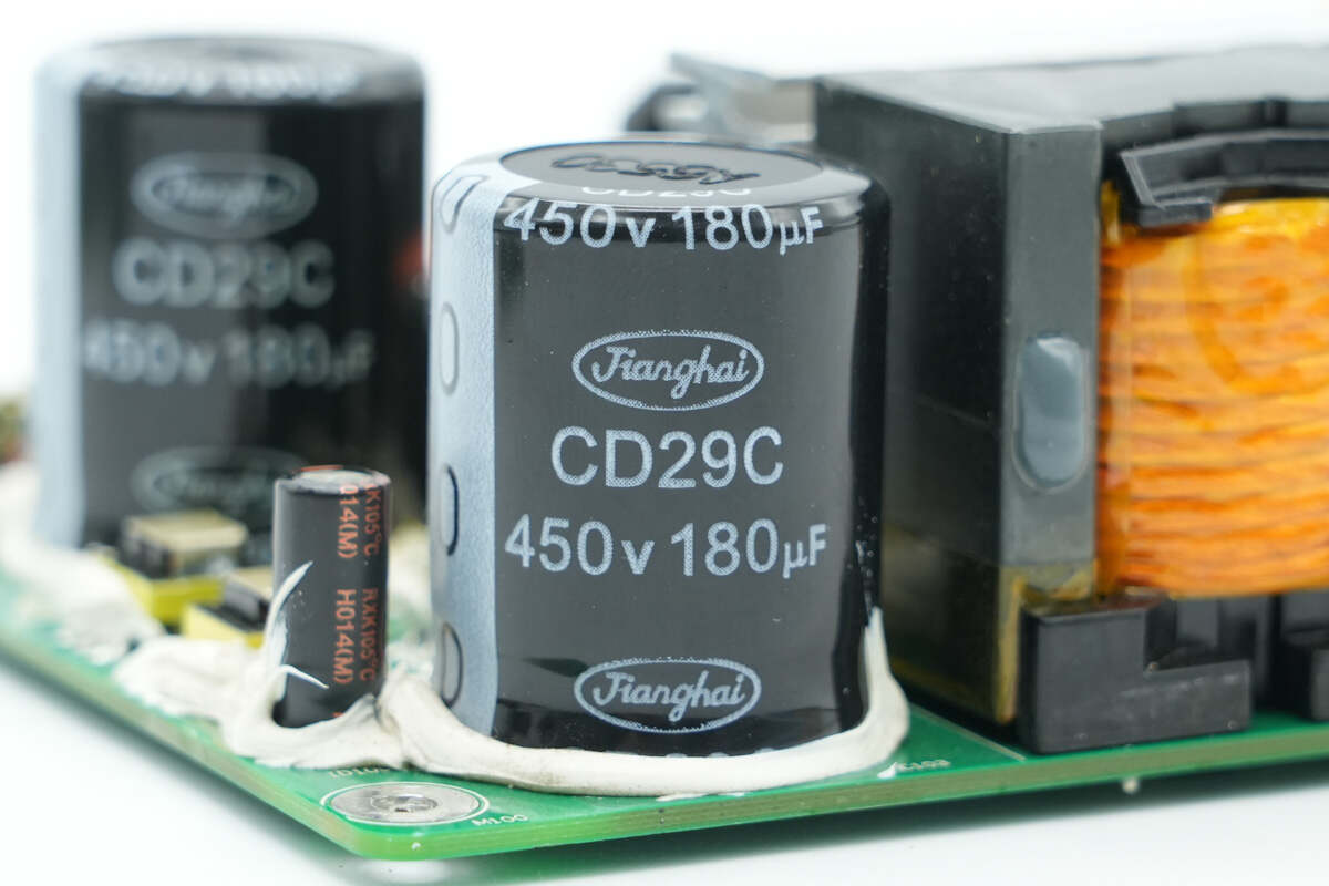
The filter capacitors are from Jianghai, model CD29C series, rated at 450V 180μF, with the bottom reinforced by adhesive.
The other filter capacitor has the same specifications.
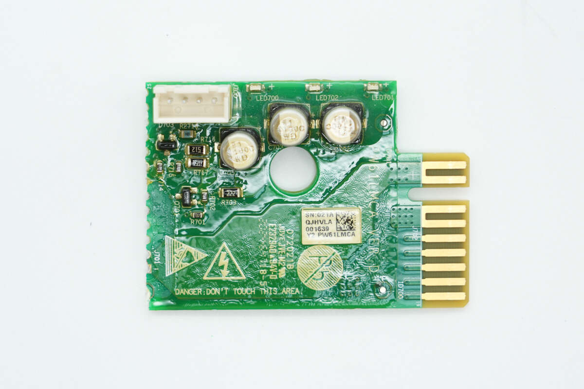
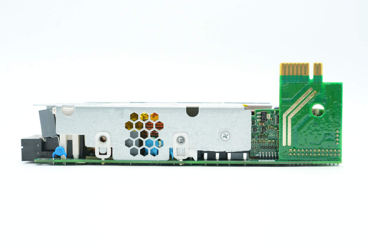
The connection PCB is soldered in place, with gold fingers located on the right side.
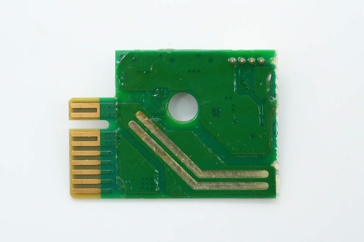
The back has exposed copper with added solder to enhance current-carrying capability.
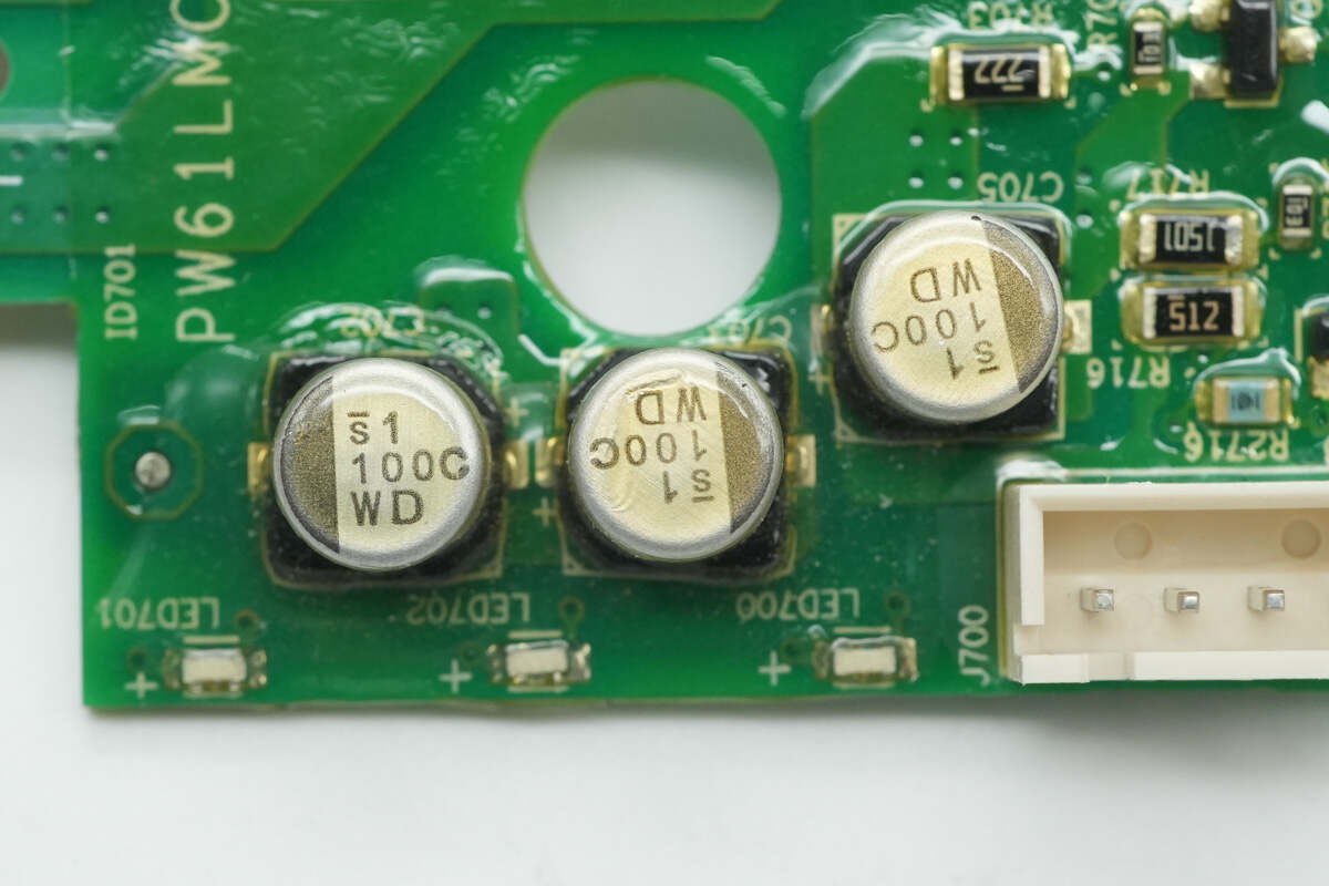
Three SMD filter capacitors, each rated at 100μF 16V, are installed above an LED status indicator.
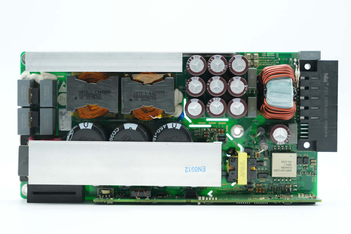
On the front side of the LLC module, the control PCB is located at the bottom, while the upper section contains the LLC MOSFETs, high-voltage filter capacitors, transformers, and synchronous rectifiers. On the left side are the resonant capacitors and resonant inductor, and on the right side are the output filter capacitor, filter inductor, and auxiliary power supply.
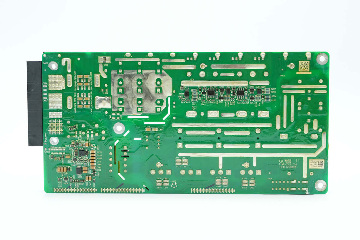
The backside is equipped with drivers, and the corresponding high-current traces feature exposed copper with added solder to enhance current-carrying capability.
The input socket and control PCB are soldered on the side.
The other side features resonant capacitors, diodes, and a resonant inductor.
This side has busbars soldered for current carrying, along with synchronous rectifiers and filter capacitors.
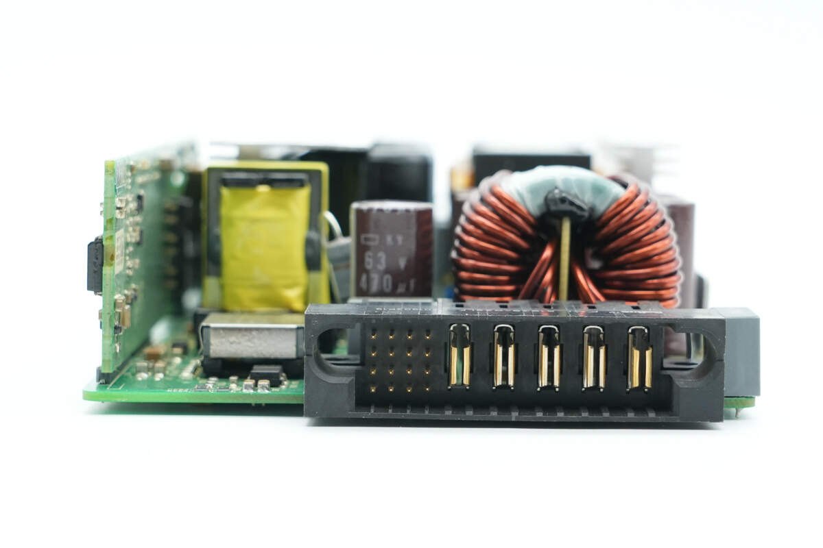
The output end features a connector socket and a filter inductor.
Remove the heatsink, then take out the diodes, filter capacitors, and the control PCB.
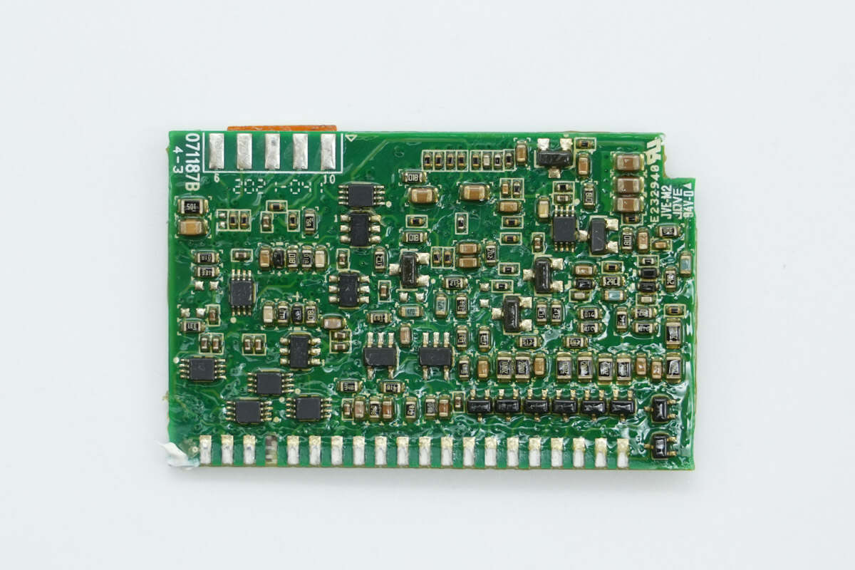
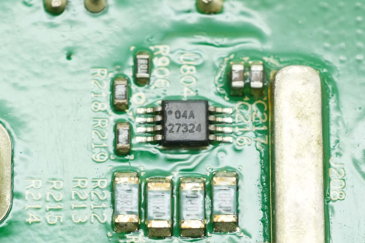
On the control PCB, the left side houses the power management chip and driver ICs, the center contains the voltage regulator, and the right side includes the operational amplifier, LLC controller, memory, and isolation chip.
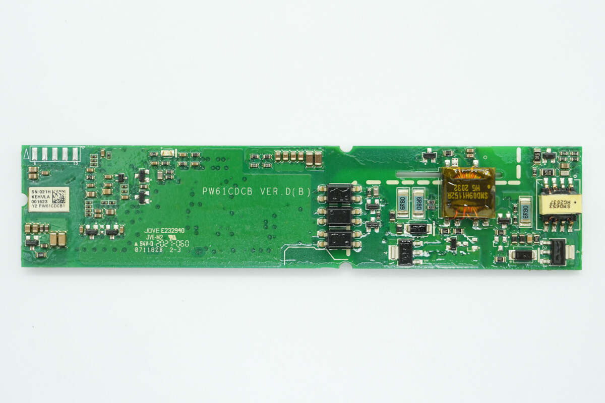
The other side features the auxiliary power transformer and driver transformer, as well as communication optocouplers.
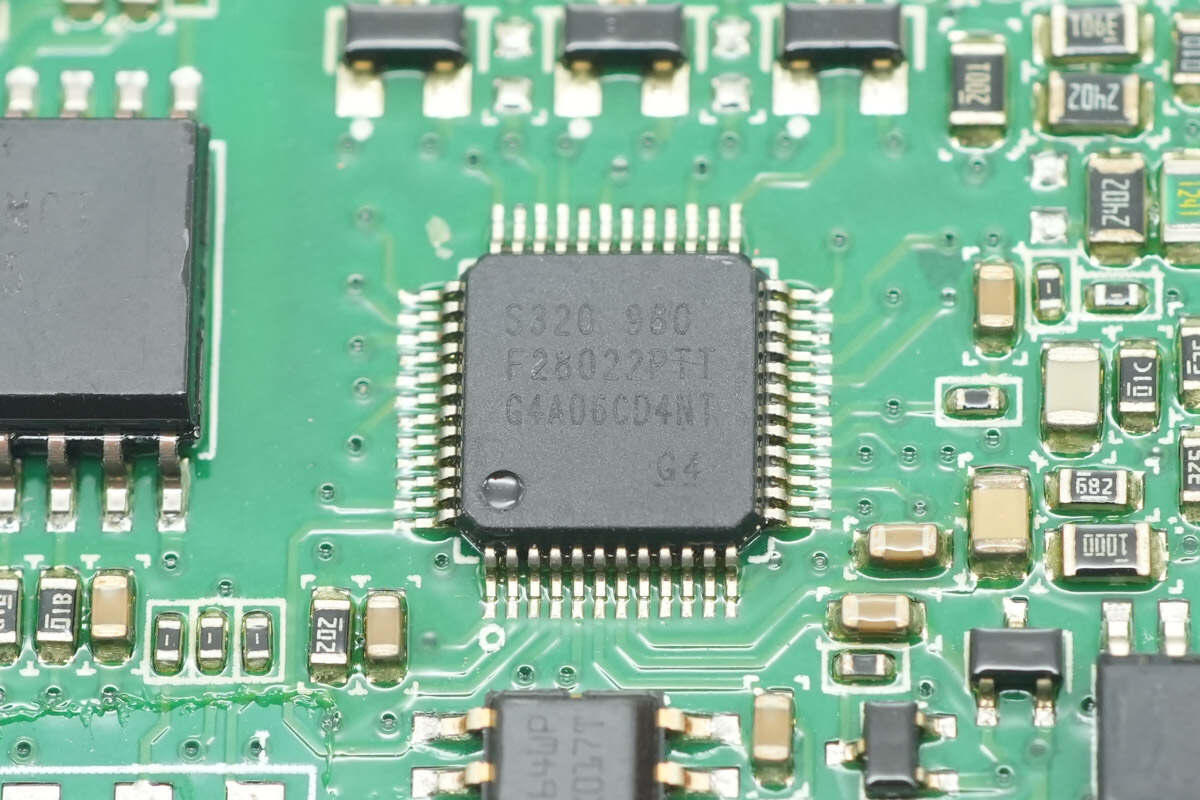
The LLC controller is the TI TMS320F28022, which is the same model as the PFC controller.
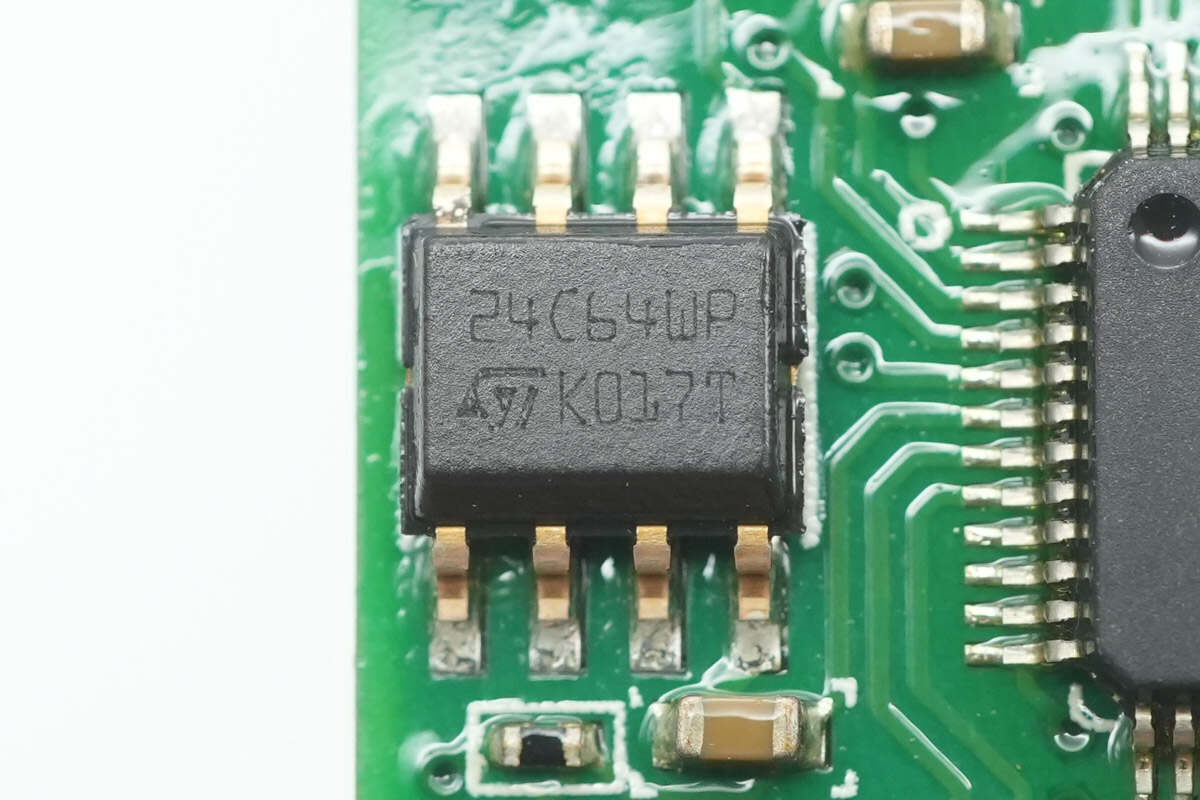
The memory is from STMicro, model M24C64-W, with a capacity of 8KB and packaged in an SO8 form factor.
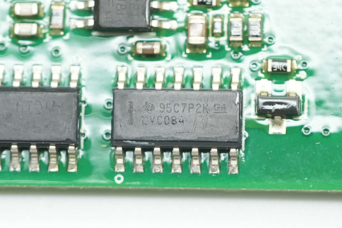
The AND gate chip is from TI, marked with LVC08A, model SN74LVC08A. It is a quad 2-input AND gate in an SOIC-14 package.
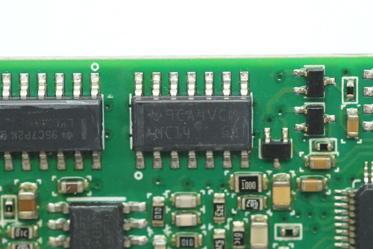
The inverter chip is from TI, marked with AHC14, model SN74AHC14. It is a hex inverter (6-channel inverter) in an SOIC-14 package.
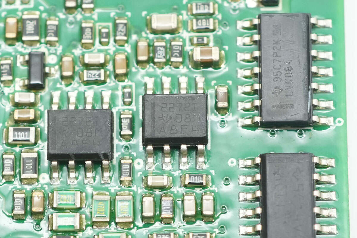
The dual operational amplifier is from TI, model TLC2272. It is a dual-channel, low-noise, rail-to-rail op-amp in an SOIC-8 package.
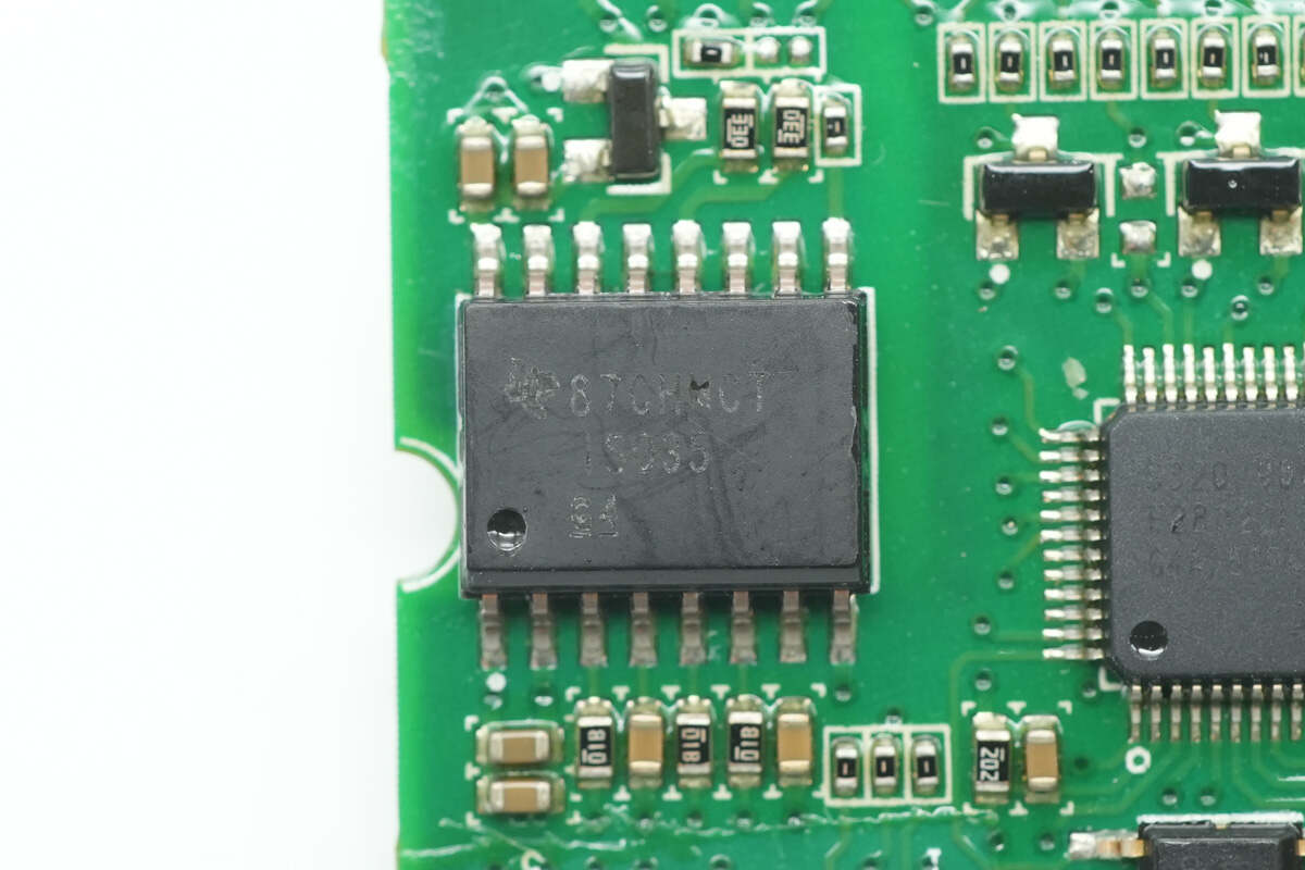
The isolation chip is from TI, model ISO35. It is used for communication isolation, supports a data rate of 1 Mbps, and provides 2.5 kVrms isolation voltage. The package is SOIC-16.
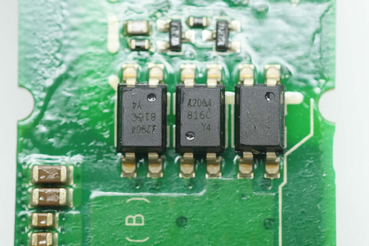
Three LITEON LTV-816C optocouplers are used for feedback isolation.
The driver is from TI, model UCC27324. It is a dual low-side gate driver with a 4A output current, packaged in an MSOP-8 PowerPAD, used for driving LLC MOSFETs.
Another driver with the same model.
A single driver is used to drive the isolation transformer.
Close-up of the isolation transformer used to drive the high-side MOSFET.
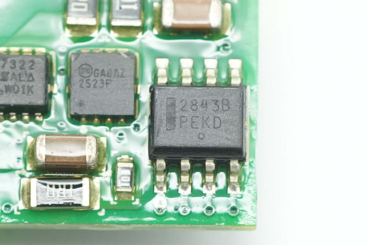
The auxiliary power chip is from Onsemi, model UC2843B. It is a high-performance PWM controller used in switching power supplies and DC-DC converter applications, packaged in an SO-8 package.
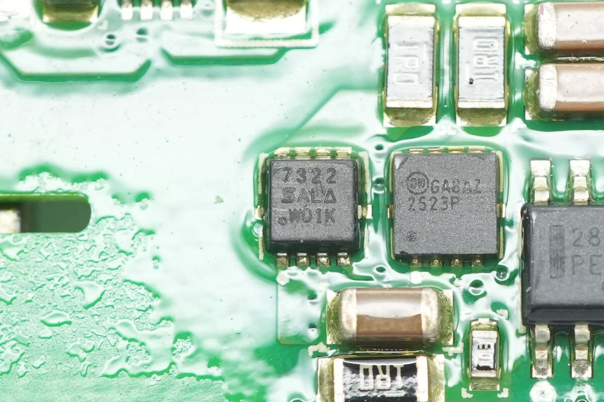
The MOSFET from VISHAY is model Si7322DN, an NMOS with a voltage rating of 100V, an on-resistance of 58mΩ, and comes in a PowerPAK 1212-8 package.
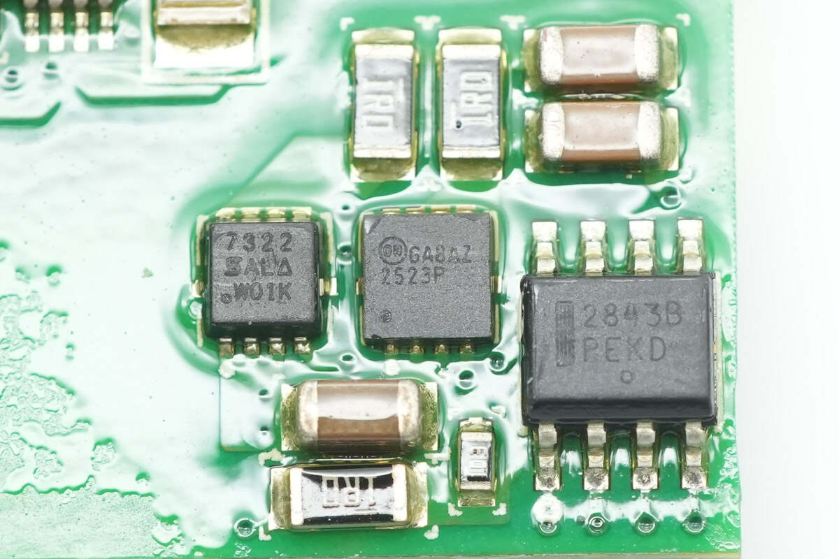
Another MOSFET from Onsemi is model FDMC2523P, a PMOS with a voltage rating of -150V, an on-resistance of 1.5Ω, and packaged in a WDFN8.
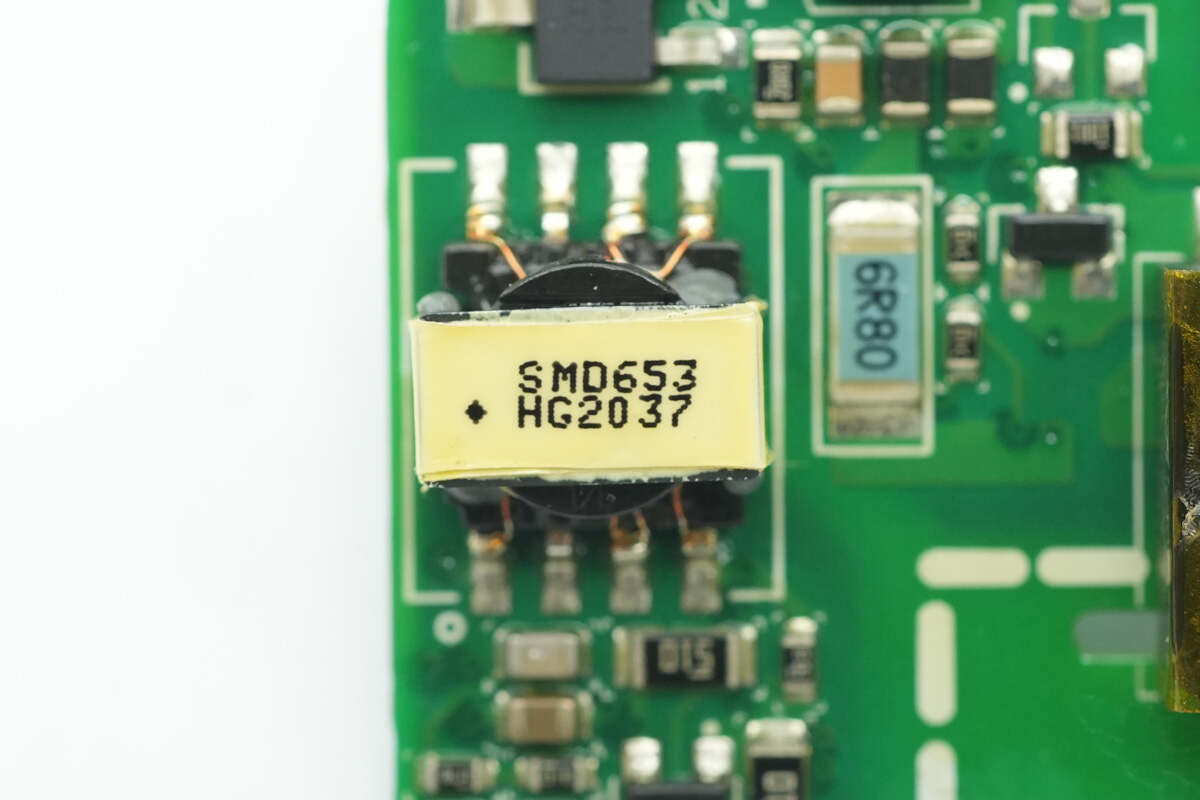
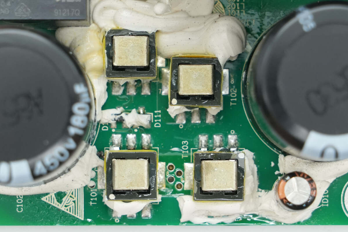
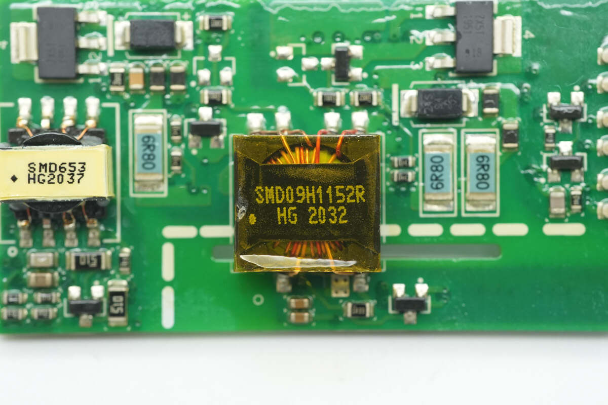
Close-up of the auxiliary power transformer.
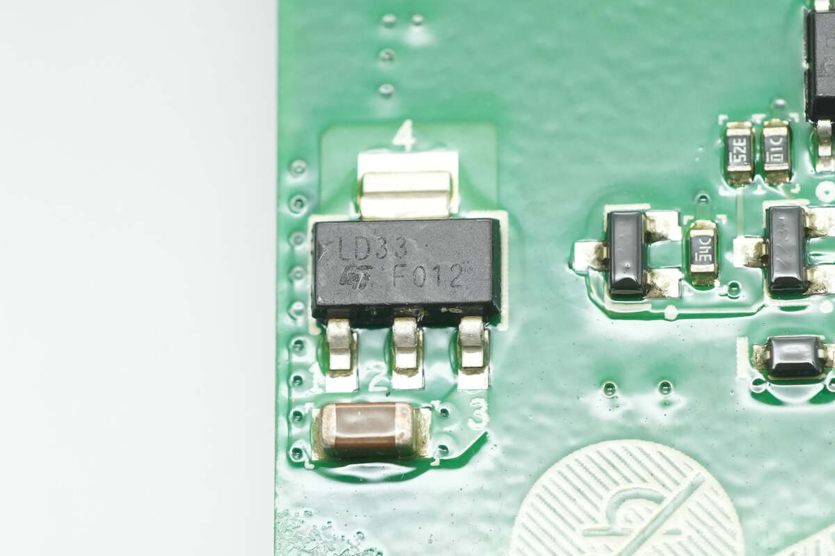
The voltage regulator chip is from STMicro, marked with LD33. It is used to supply power to the LLC controller and comes in a SOT-223 package.
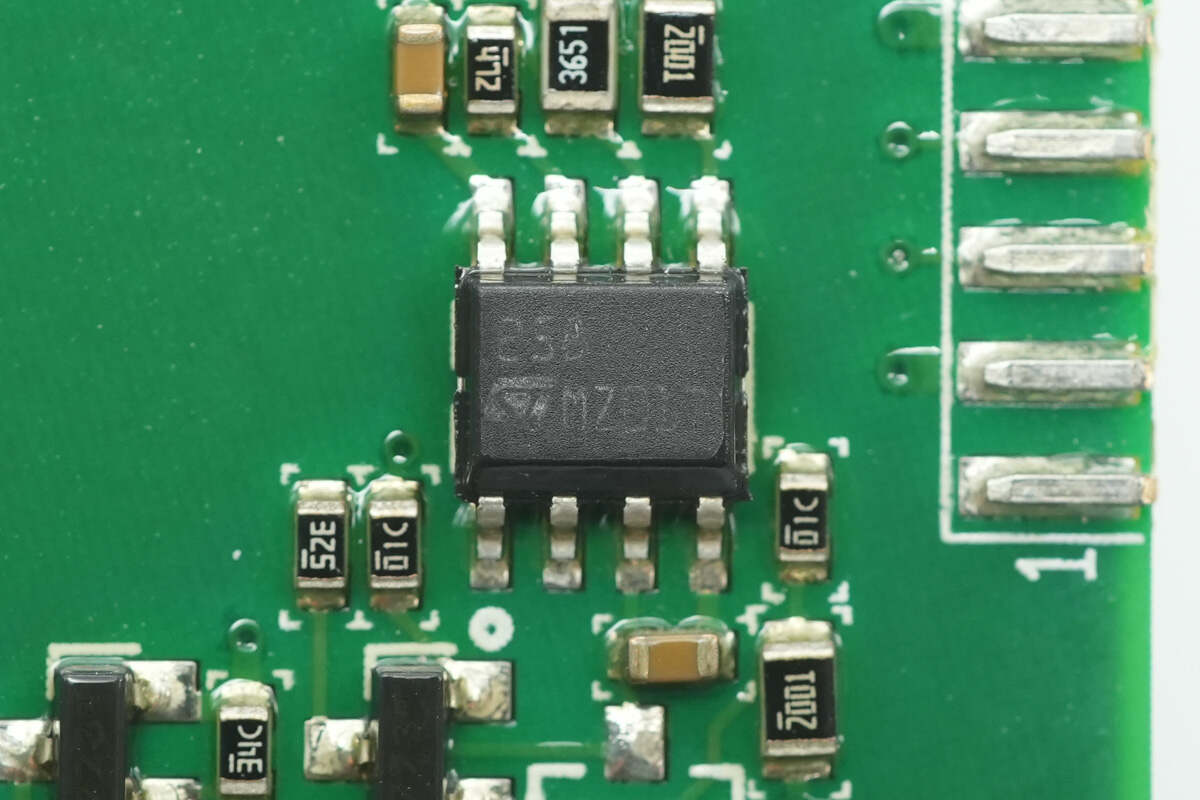
Close-up of the STMicro LM258 dual operational amplifier.
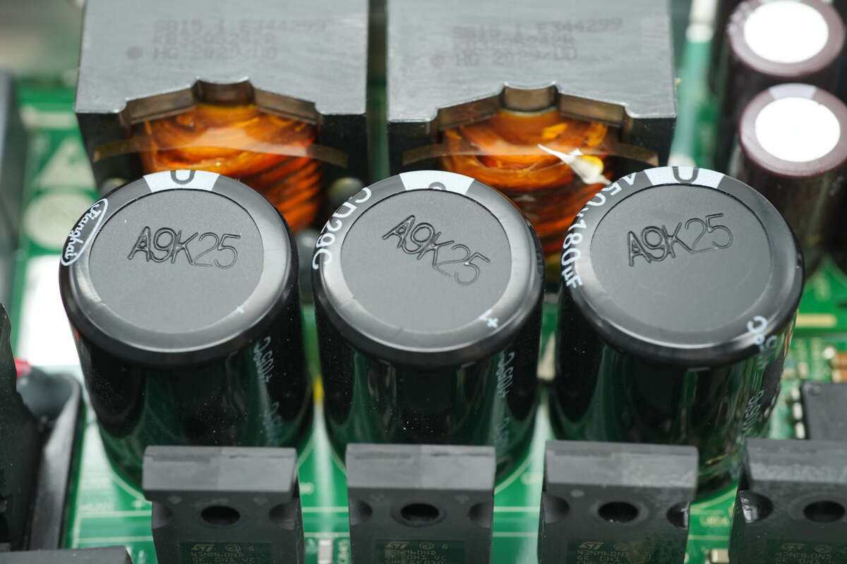
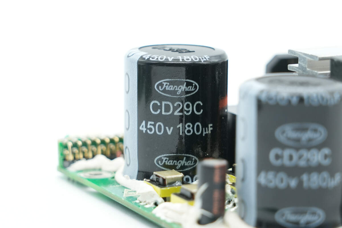
The LLC module is equipped with three filter capacitors.
The filter capacitors are from Jianghai, rated at 450V 180μF.
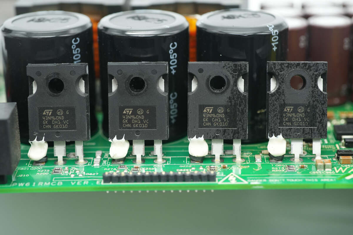
Four MOSFETs are mounted on the heatsink.
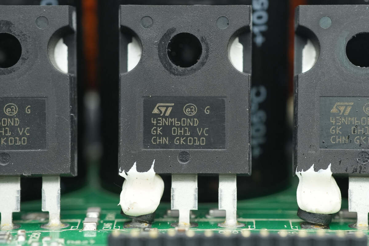
The MOSFET is from STMicro, model STW43NM60ND, the same model as the PFC MOSFET.
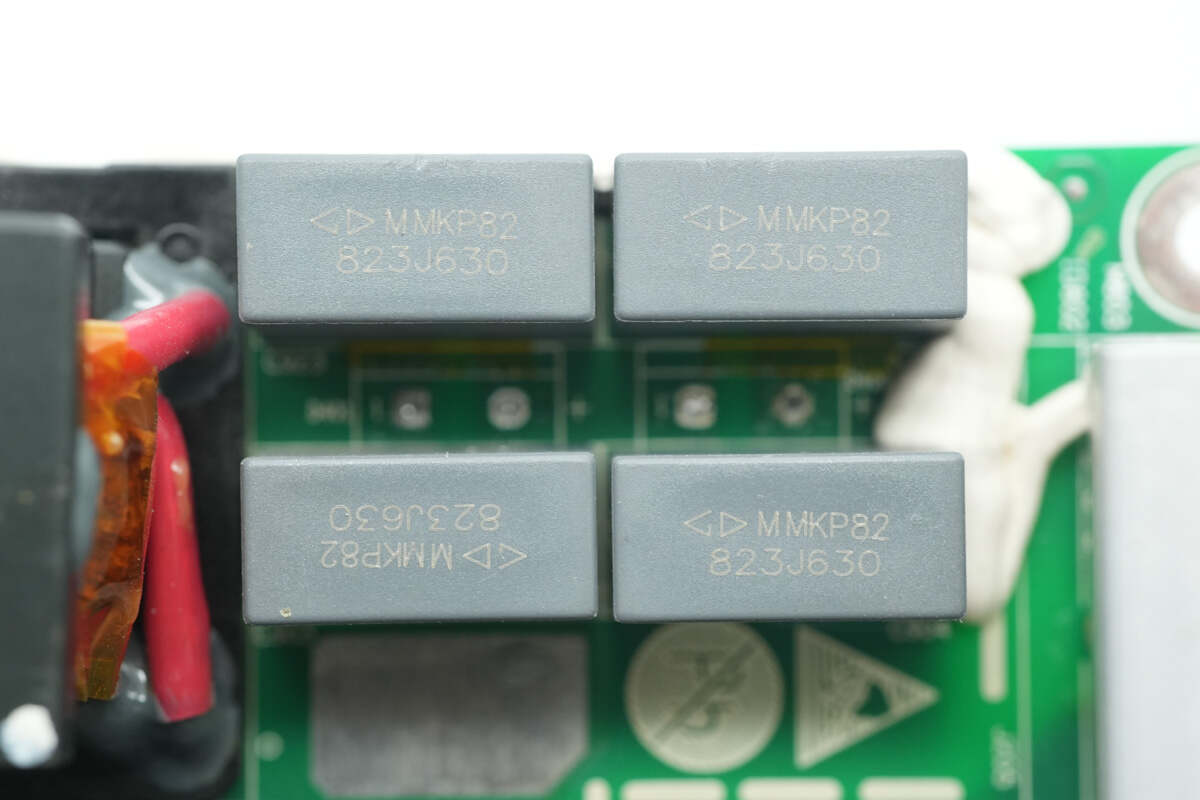
The resonant capacitors are from Faratronic, rated at 0.082μF 630V. There are four capacitors connected in a configuration of two in series and two in parallel.
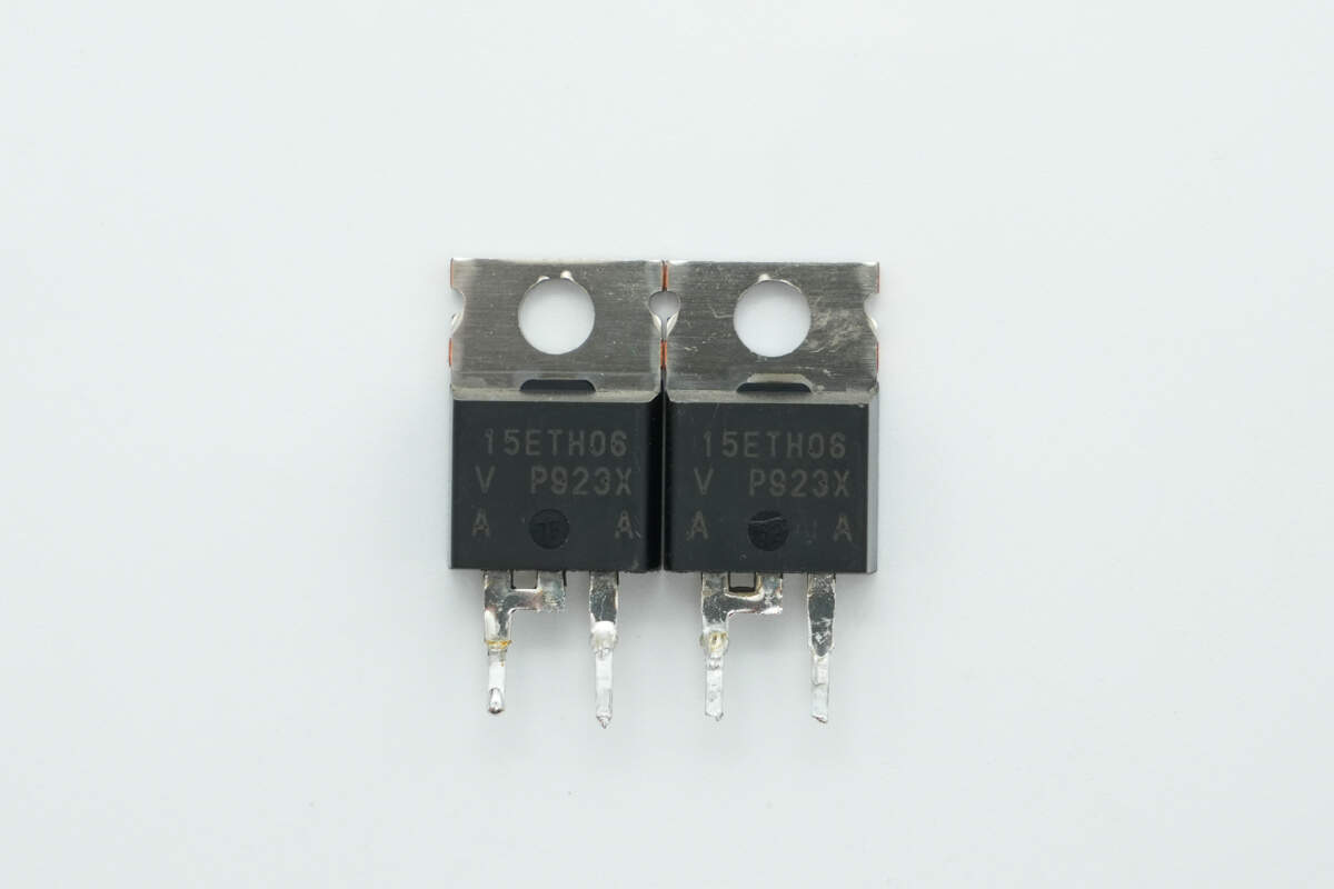
Two ultrafast recovery diodes are from VISHAY, model VS-15ETH06-M3, rated at 600V 15A, and packaged in 2-lead TO-220AC.
Close-up of the resonant inductor.
The LLC transformer is wound with Litz wire.
Close-up of the TI UCC27324 low-side driver.
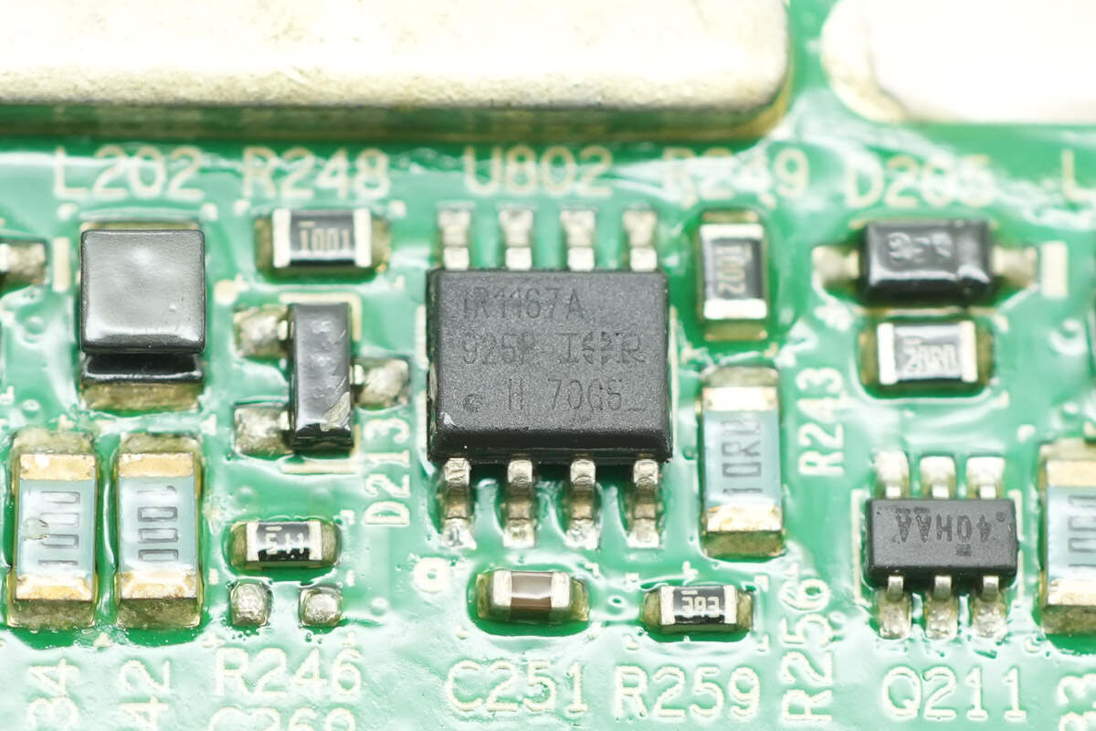
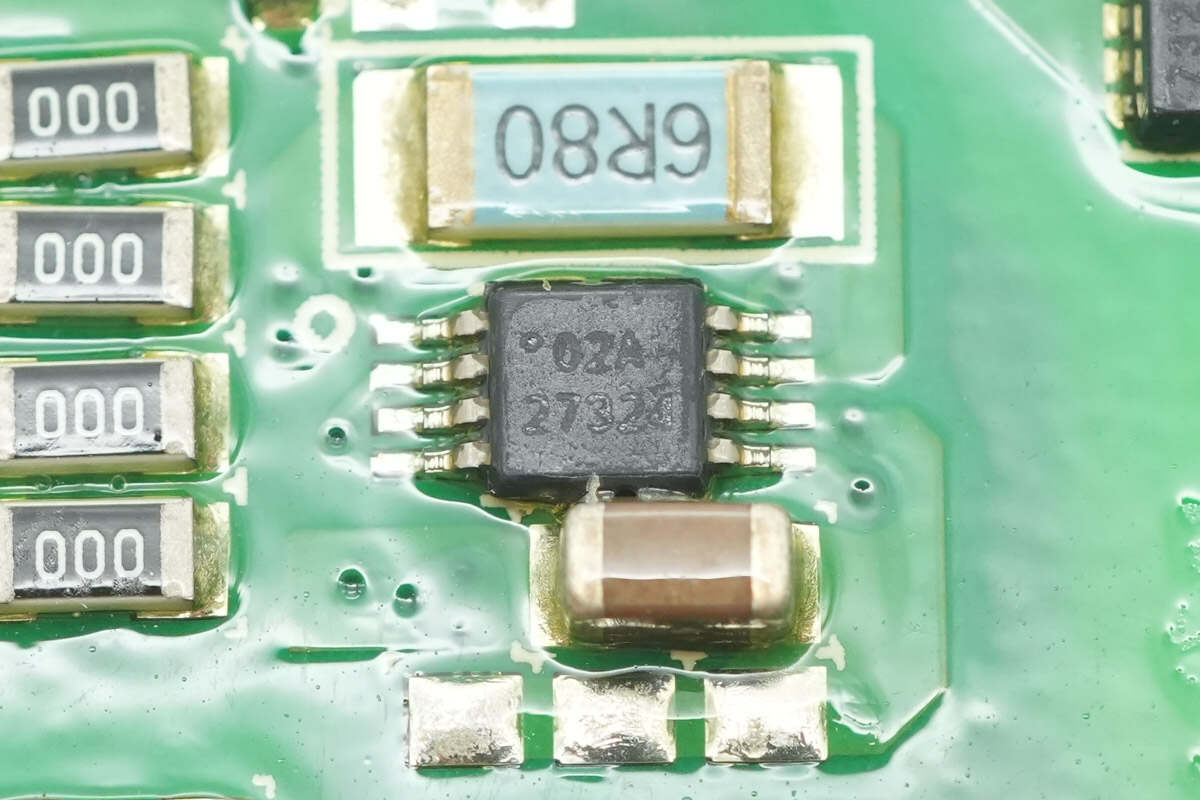
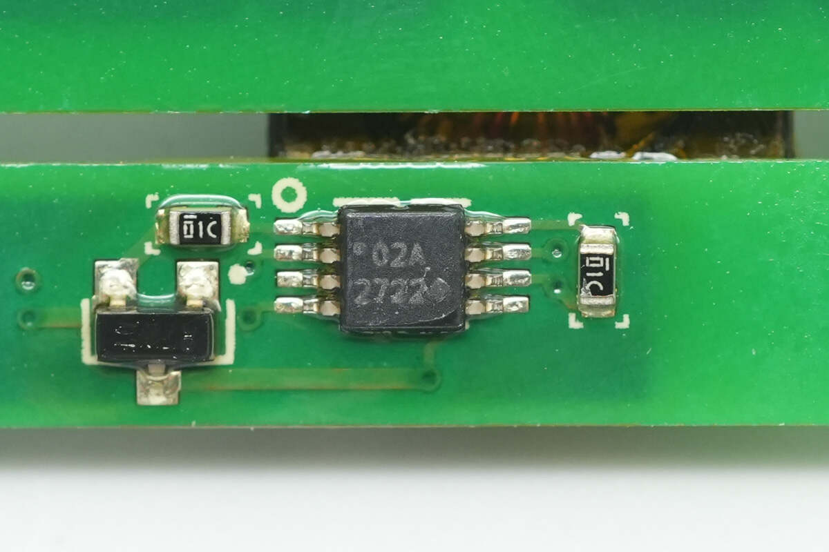
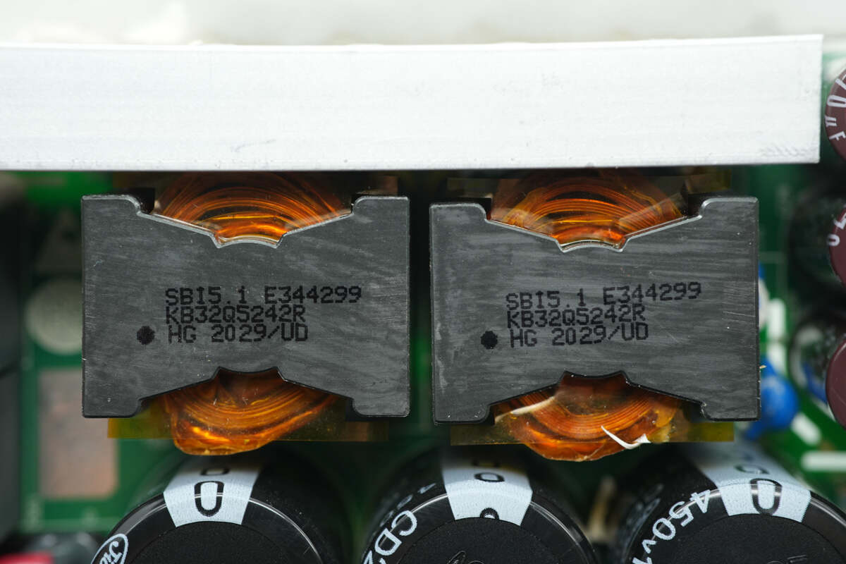
The synchronous rectification controller is from Infineon, model IR1167A. It supports DCM, CrCM, and CCM modes, operates at switching frequencies up to 500 kHz, and comes in an SOIC-8N package.
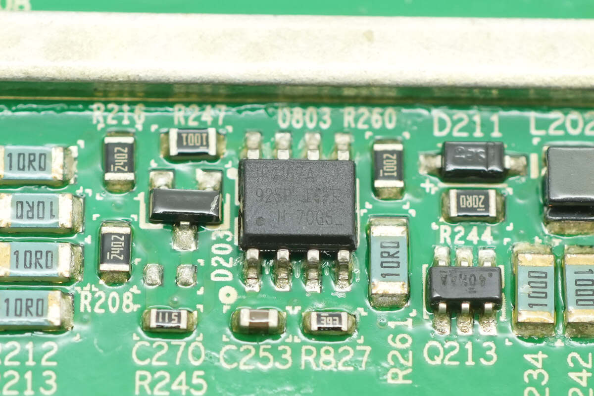
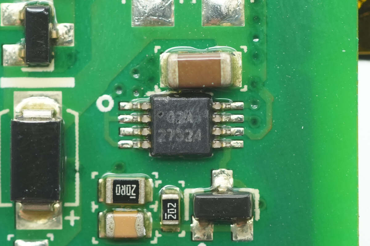
Another synchronous rectification controller with the same model.
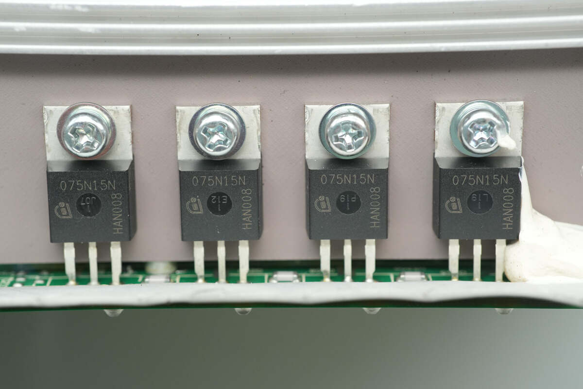
Four synchronous rectifiers are mounted on the heatsink.
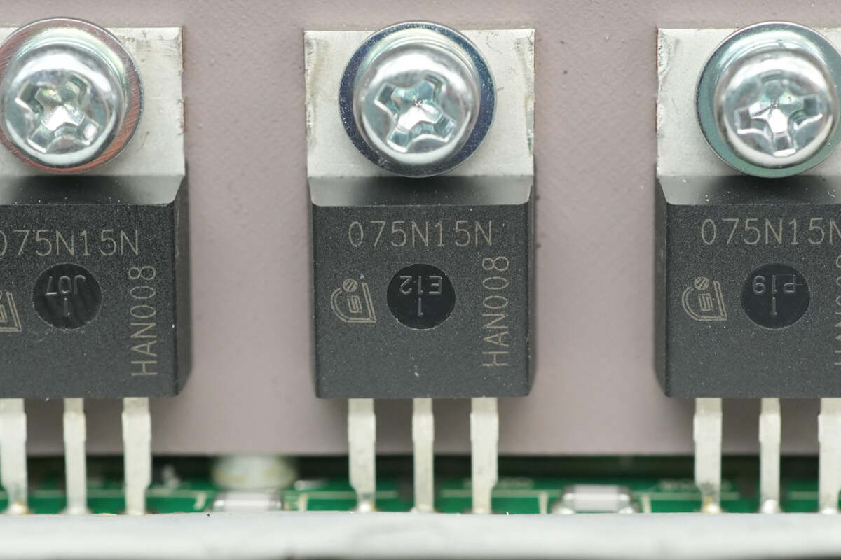
The synchronous rectifier is from Infineon, model IPP075N15N3-G. It is an NMOS with a voltage rating of 150V, an on-resistance of 7.2mΩ, and comes in a TO-220-3 package.
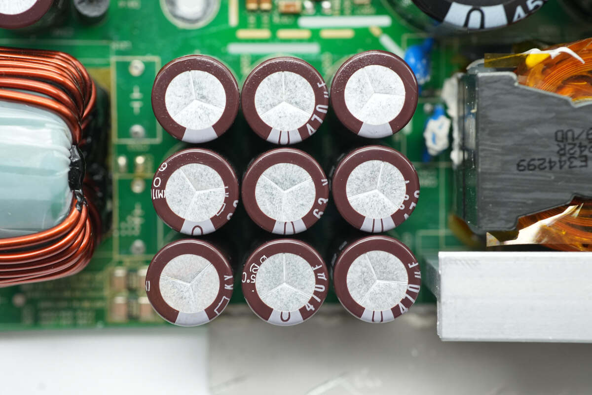
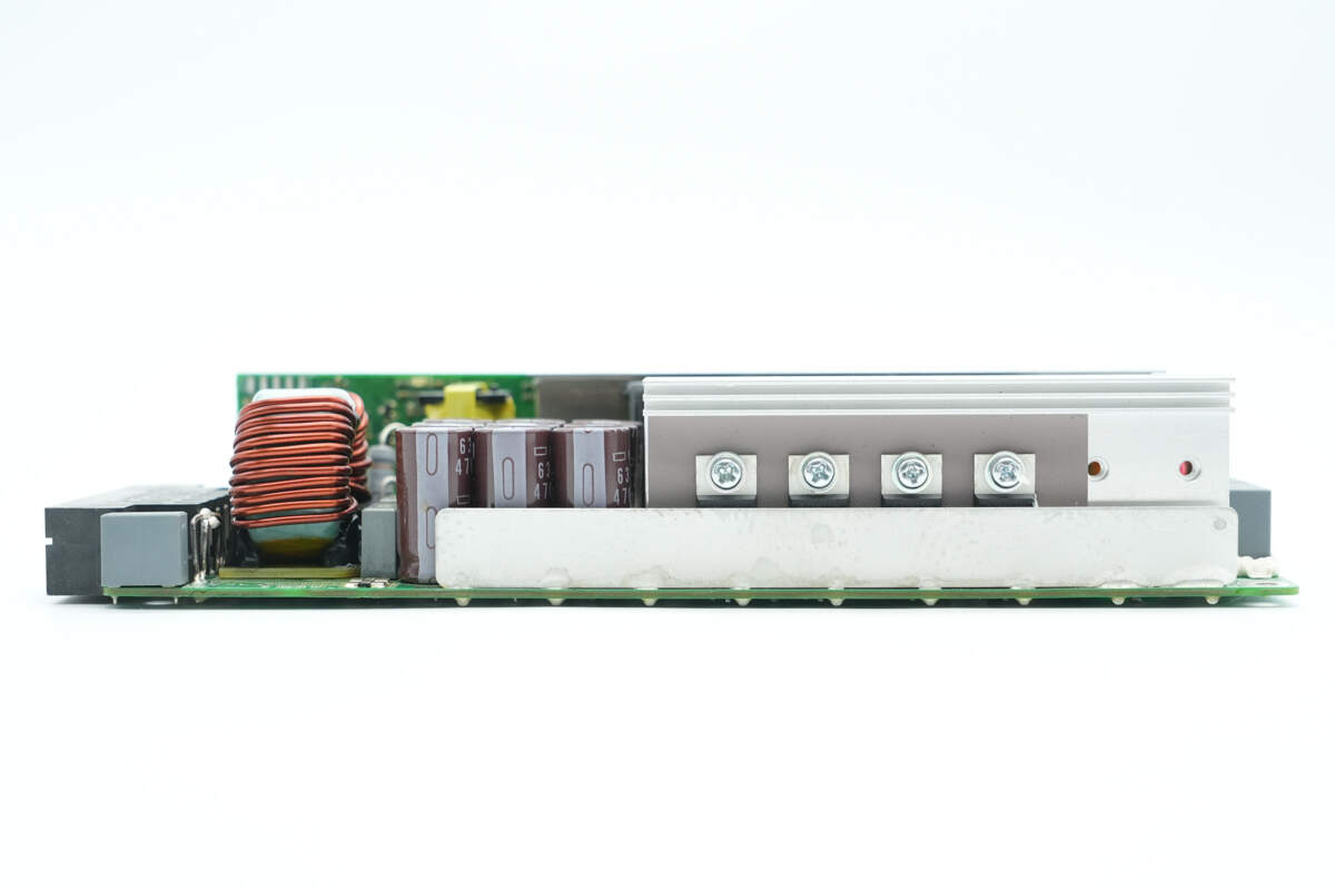
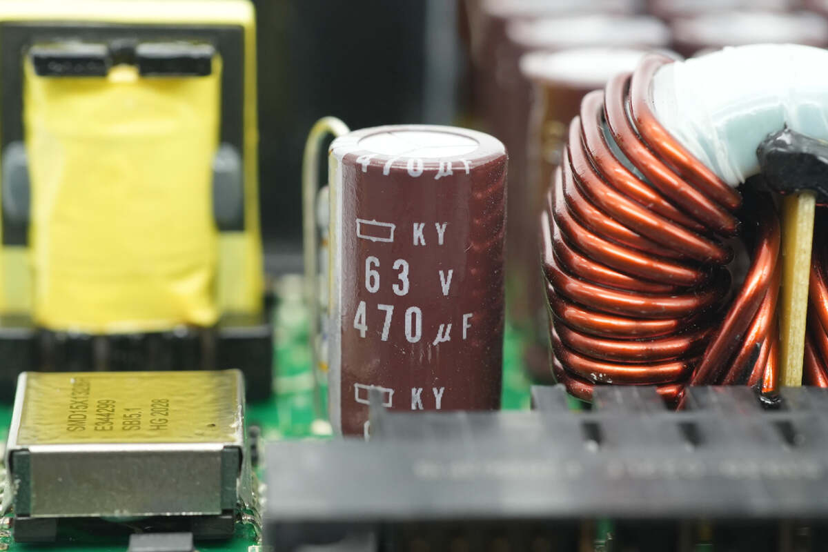
Nine filter capacitors are installed at the output.
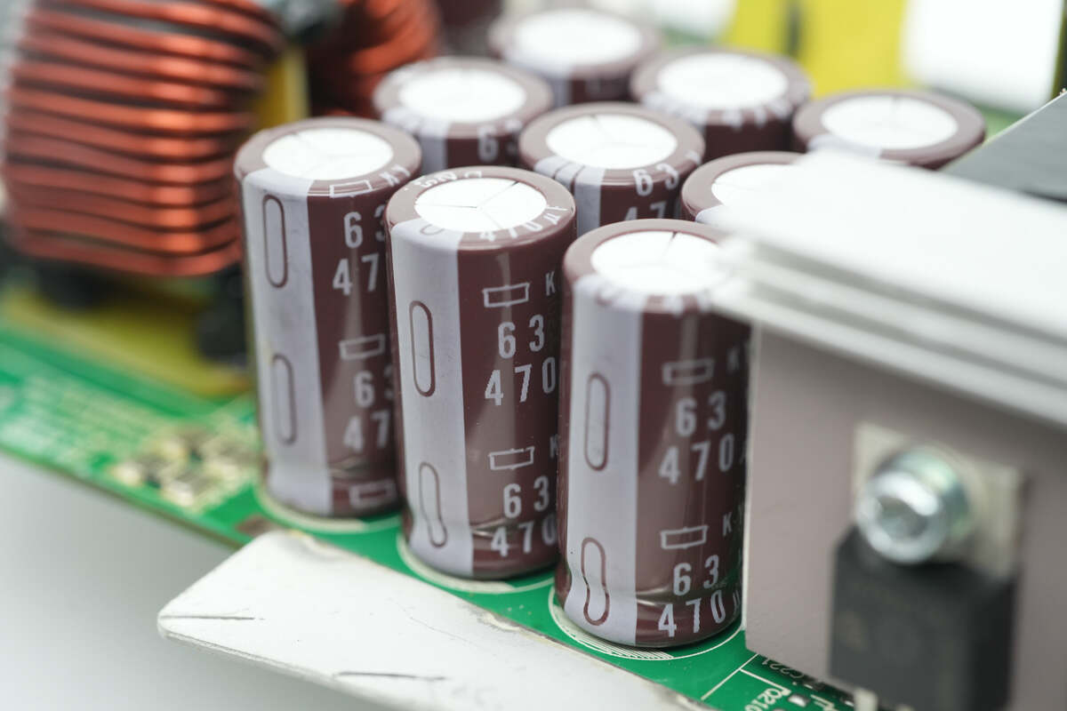
The capacitors are from NCC, rated at 63V 470μF.
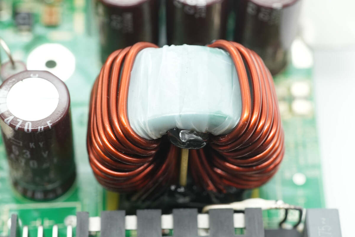
The filter inductor is wound with a magnetic core.
Three film capacitors, each rated at 0.1μF.
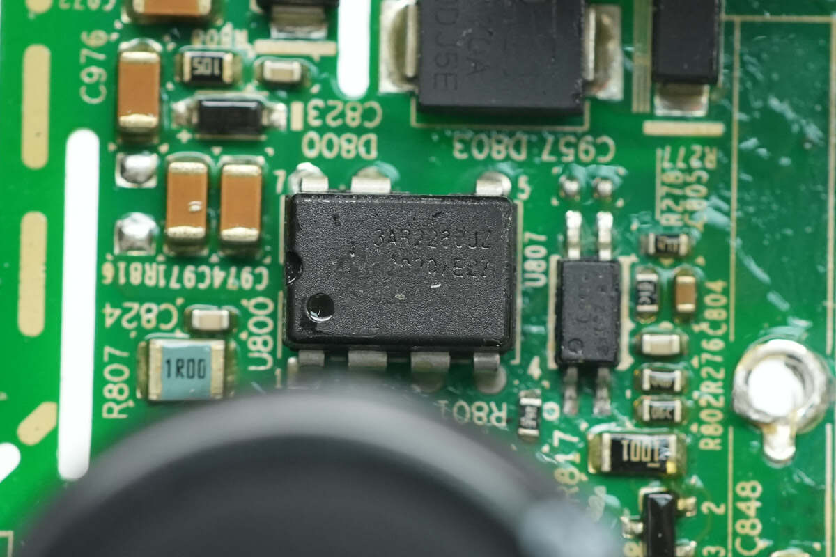
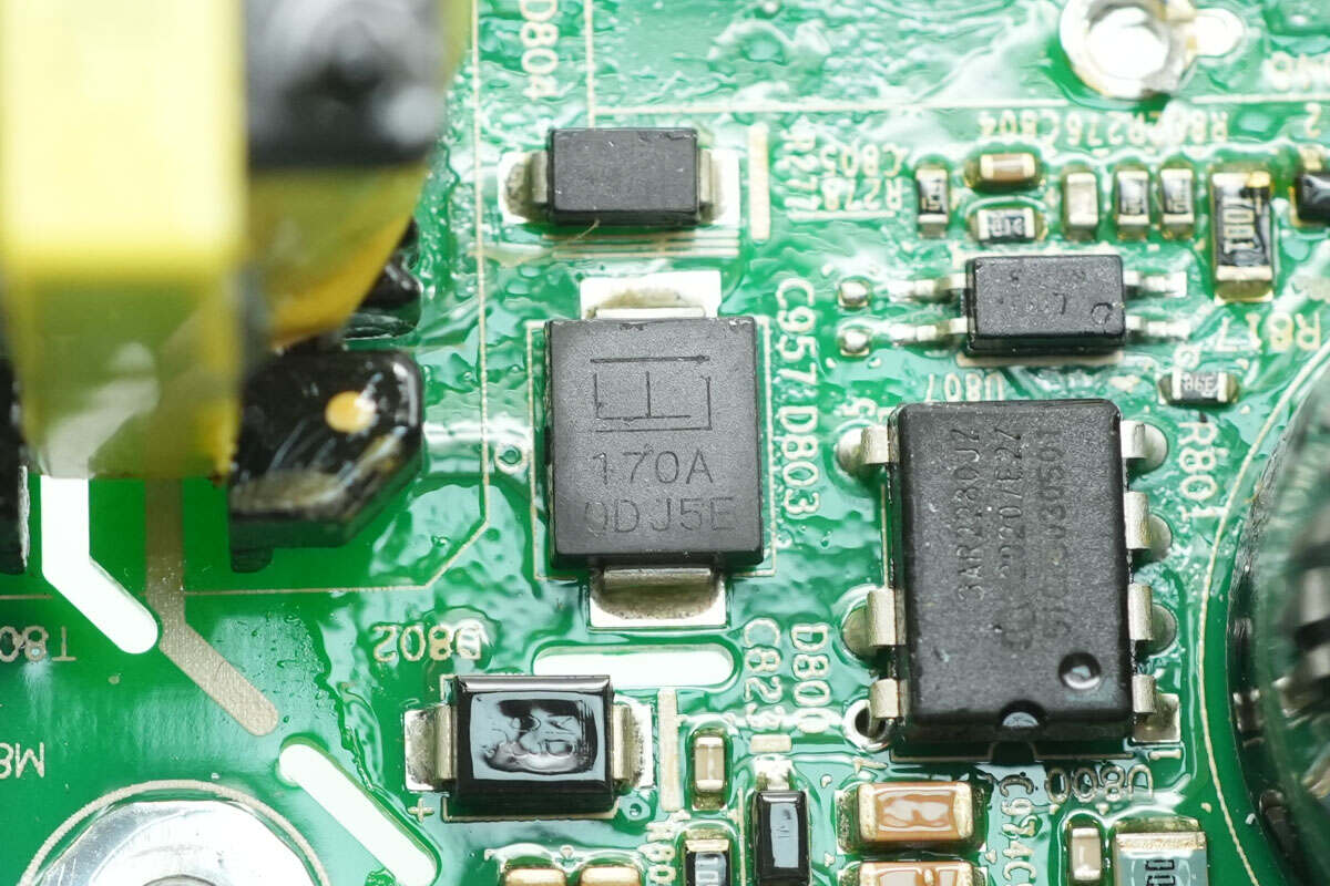
The auxiliary power chip is from Infineon, model ICE3AR2280JZ. It integrates an 800V-rated MOSFET, a startup unit, and a fixed-frequency flyback controller. It features enhanced active burst mode, comprehensive protection functions, supports 24W applications, and comes in a DIP-7 package.
Close-up of a TVS diode used for overvoltage protection.
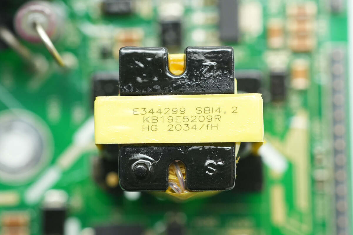
Close-up of the auxiliary power transformer.
Close-up of the output rectifier diode.
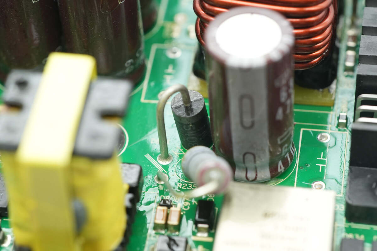
The capacitor used for output filtering has a rated voltage of 63V and a capacitance of 470μF.
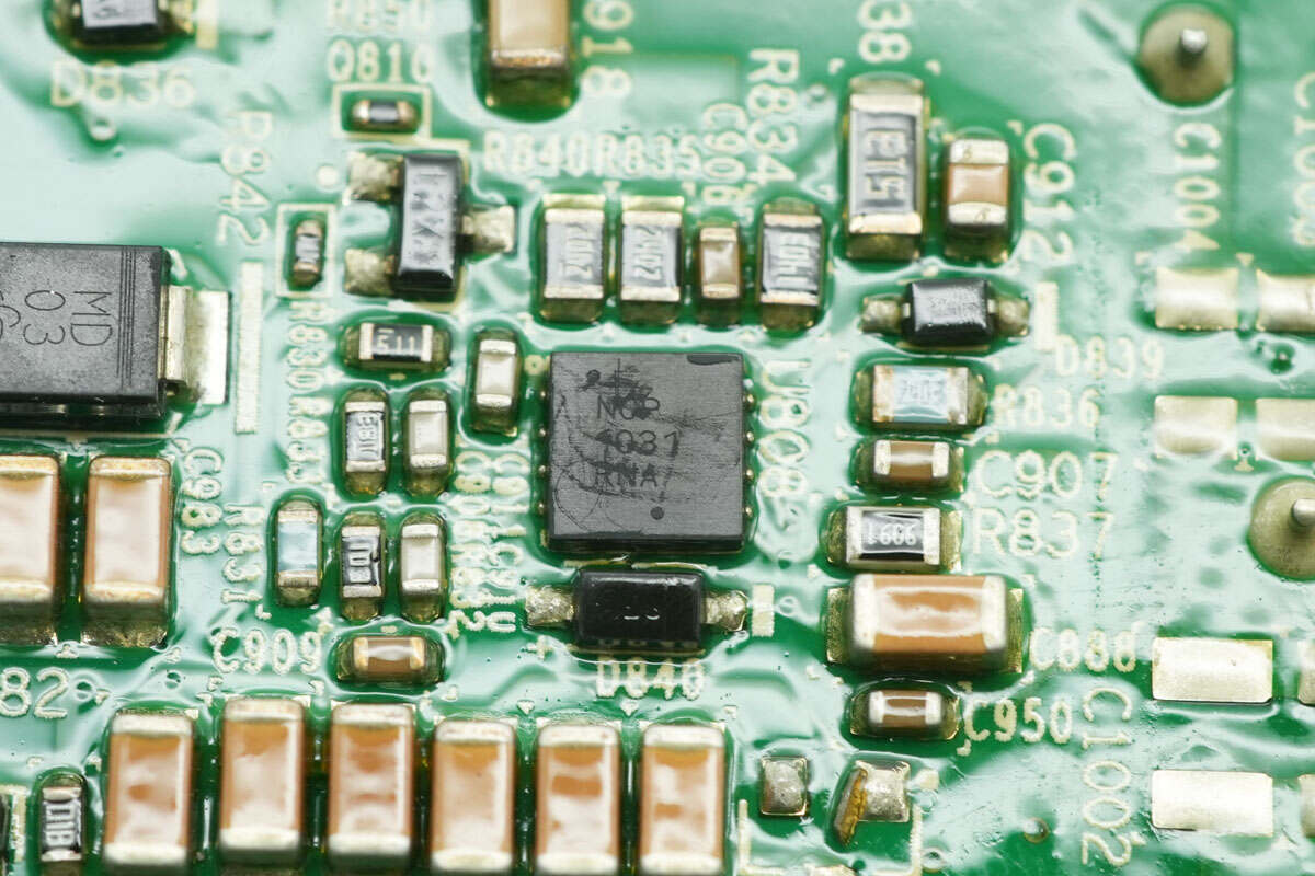
Another power supply controller chip uses the Onsemi NCP1031. The chip integrates an internal MOSFET and current-sensing resistor. It features a built-in 200V-rated MOSFET and startup circuit, making it suitable for 48V telecom applications, 42V automotive applications, and 12V input applications. The chip supports an output power of 6W and comes in a DFN-8 package.
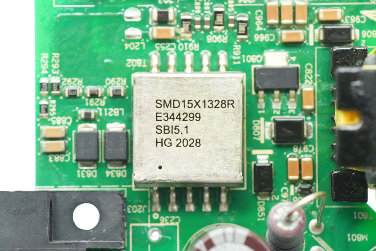
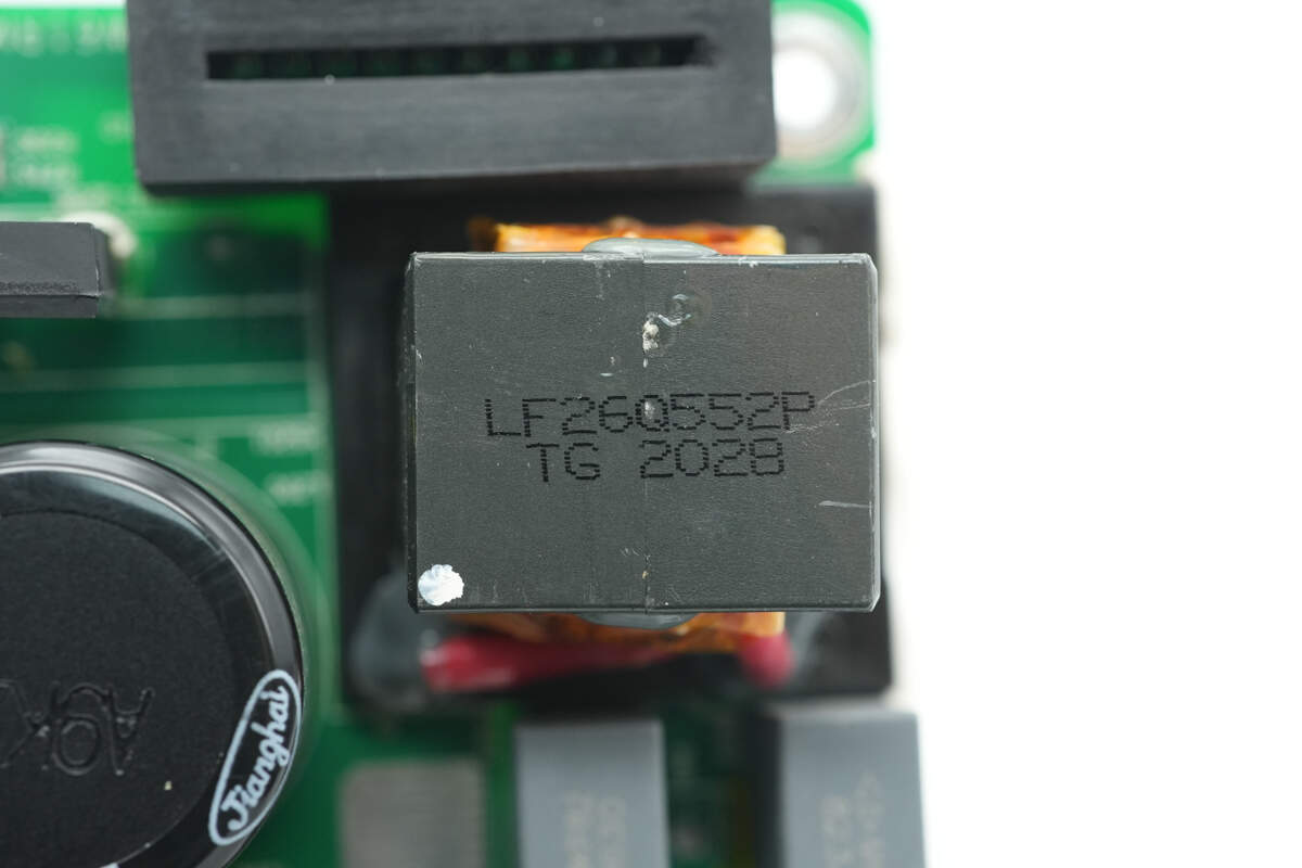
The transformer is enclosed in a shielding cover.
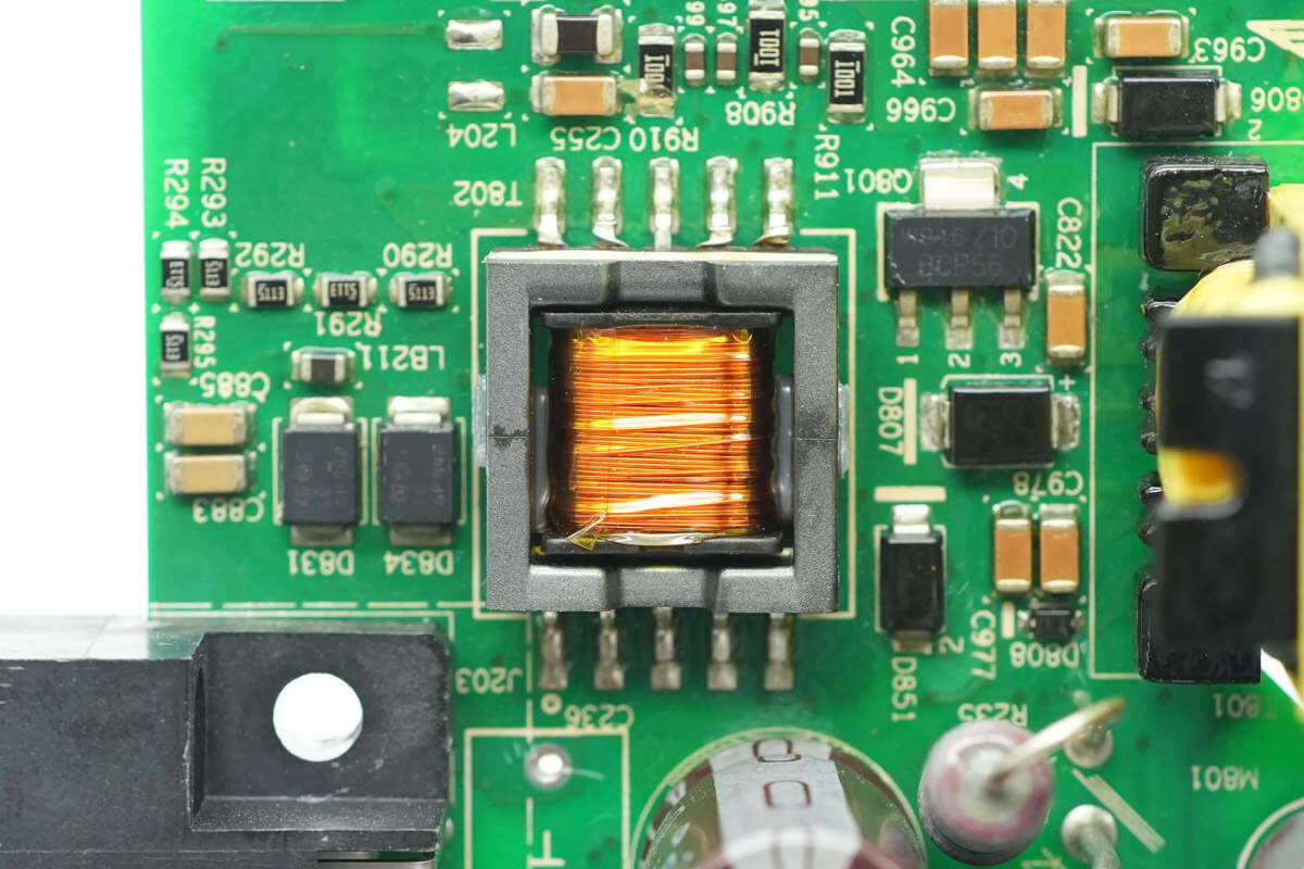
Remove the shielding cover to reveal a close-up of the internal magnetic core and coils.
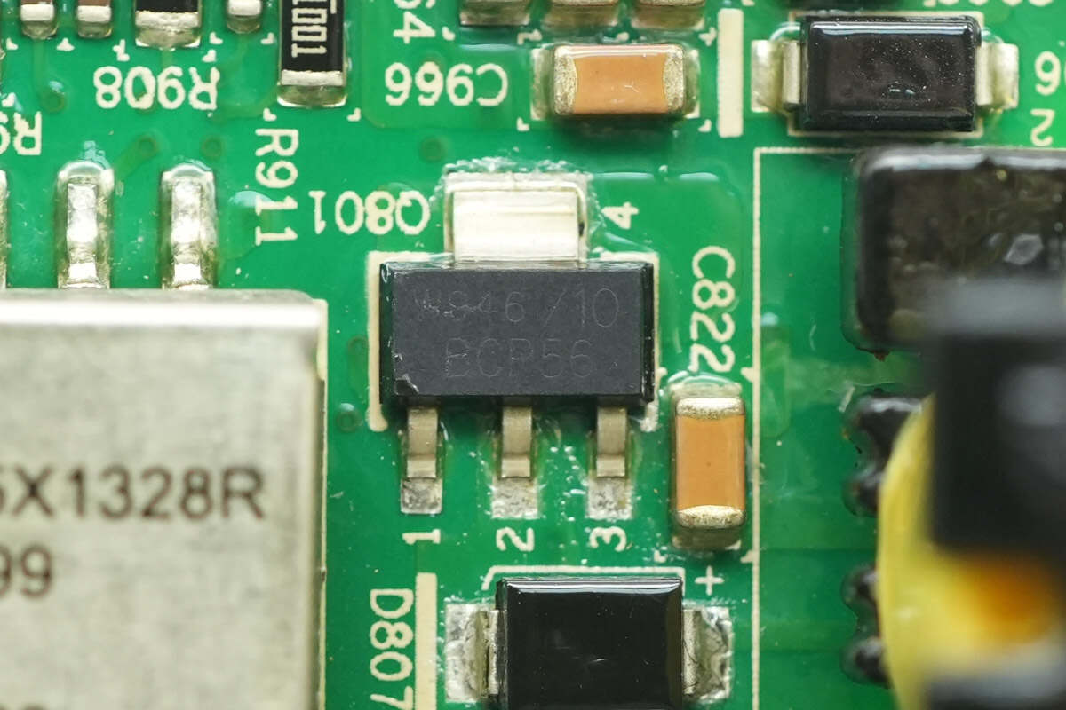
Close-up of a BCP56 transistor.
Well, those are all components of the HUAWEI 3000W R4850G1 Power Supply Unit.
Summary of ChargerLAB
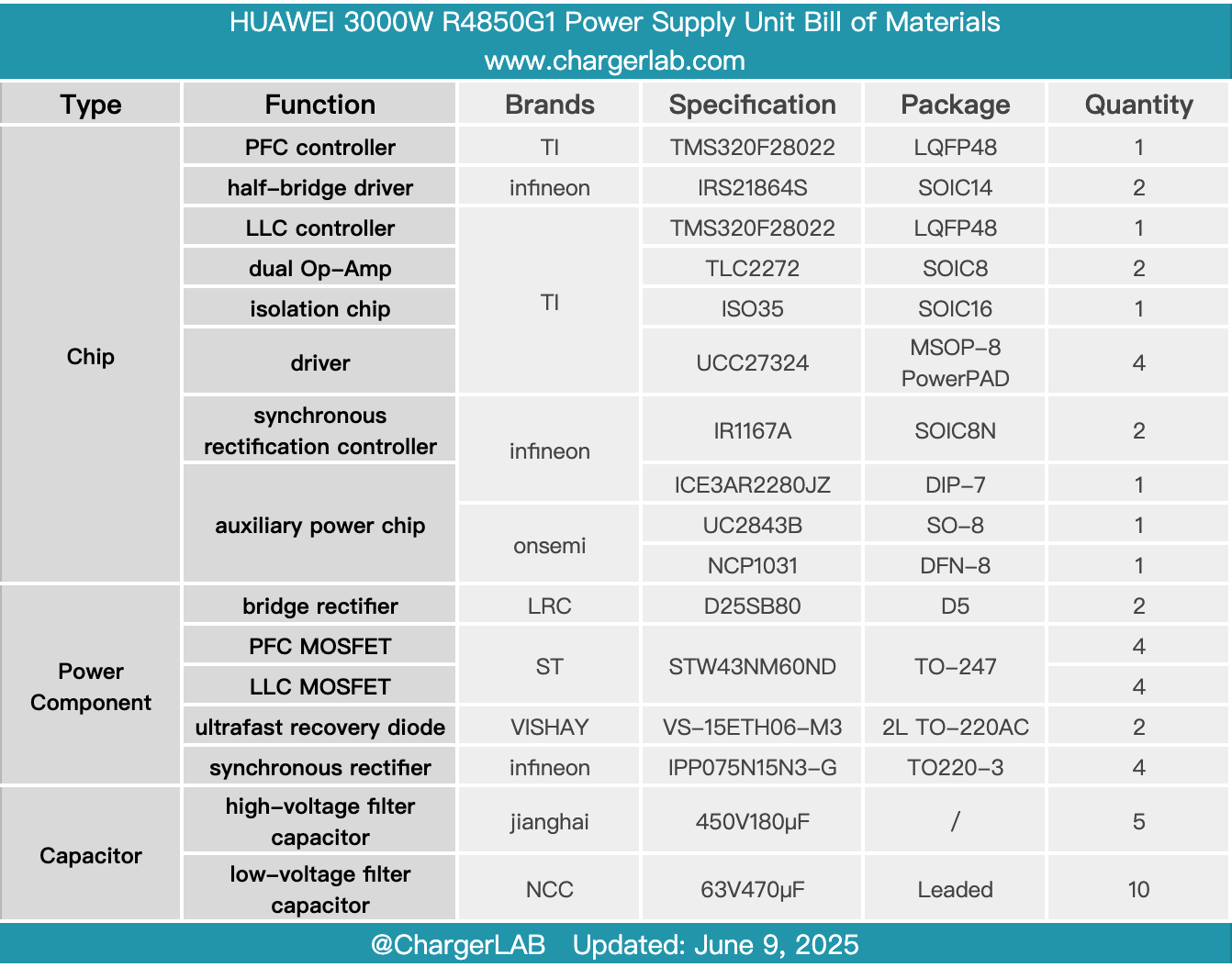
Here is the component list of the HUAWEI 3000W R4850G1 Power Supply Unit for your convenience.
It features a metal casing secured with screws. The rated input voltage is 200–240V, with an output power of 3000W. When operating at low input voltage, the output power is 1200W. The front end is equipped with a cooling fan and indicator lights, while the rear end has connectors for AC input, DC output, and communication interfaces.
After taking it apart, we found that it uses a PFC + LLC architecture with two built-in PCBA modules connected via plug-in connectors. The PFC controller employs a TI TMS320F28022 controller paired with an Infineon IRS21864S half-bridge driver. The LLC controller is the same model, used together with a TI UCC27324 driver.
The PFC and LLC MOSFETs use the STMicro STW43NM60D, while the synchronous rectifier employs the Infineon IPP075N15N3-G. The high-voltage capacitors are sourced from Jianghai, and the capacitors for output filtering come from NCC. The control PCB is vertically mounted to make full use of space and reduce the overall size. All components are coated with conformal protective coating, and the internal workmanship and materials are solid and reliable.
Related Articles:
1. Teardown of CUKTECH 10 GaN Charger Ultra (AD1204U)
2. Teardown of Huawei WATCH 2nd-Gen Wireless SuperCharger (CW05)
3. Teardown of xFusion’s FusionWatt 2000W Platinum Server Power Supply