Introduction
Most original HONOR chargers feature a single USB-A output. While they can deliver fast charging for HONOR smartphones, they are unable to meet the charging needs of devices such as laptops that rely on USB-C interfaces. To address this usage gap, HONOR officially introduced a 66W dual-port GaN charger.
The charger features one USB-A port and one USB-C port. The USB-A port supports HONOR 66W SuperCharge, while the USB-C port supports 65W PD. Below, we take a closer look at the detailed design of the product.
Product Appearance
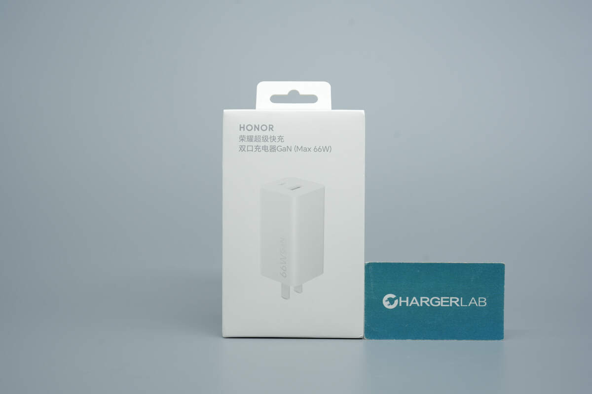
The front of the packaging box features the HONOR branding, the product name, and an image of the charger.

The back of the packaging displays key selling points, specifications, and other relevant information.
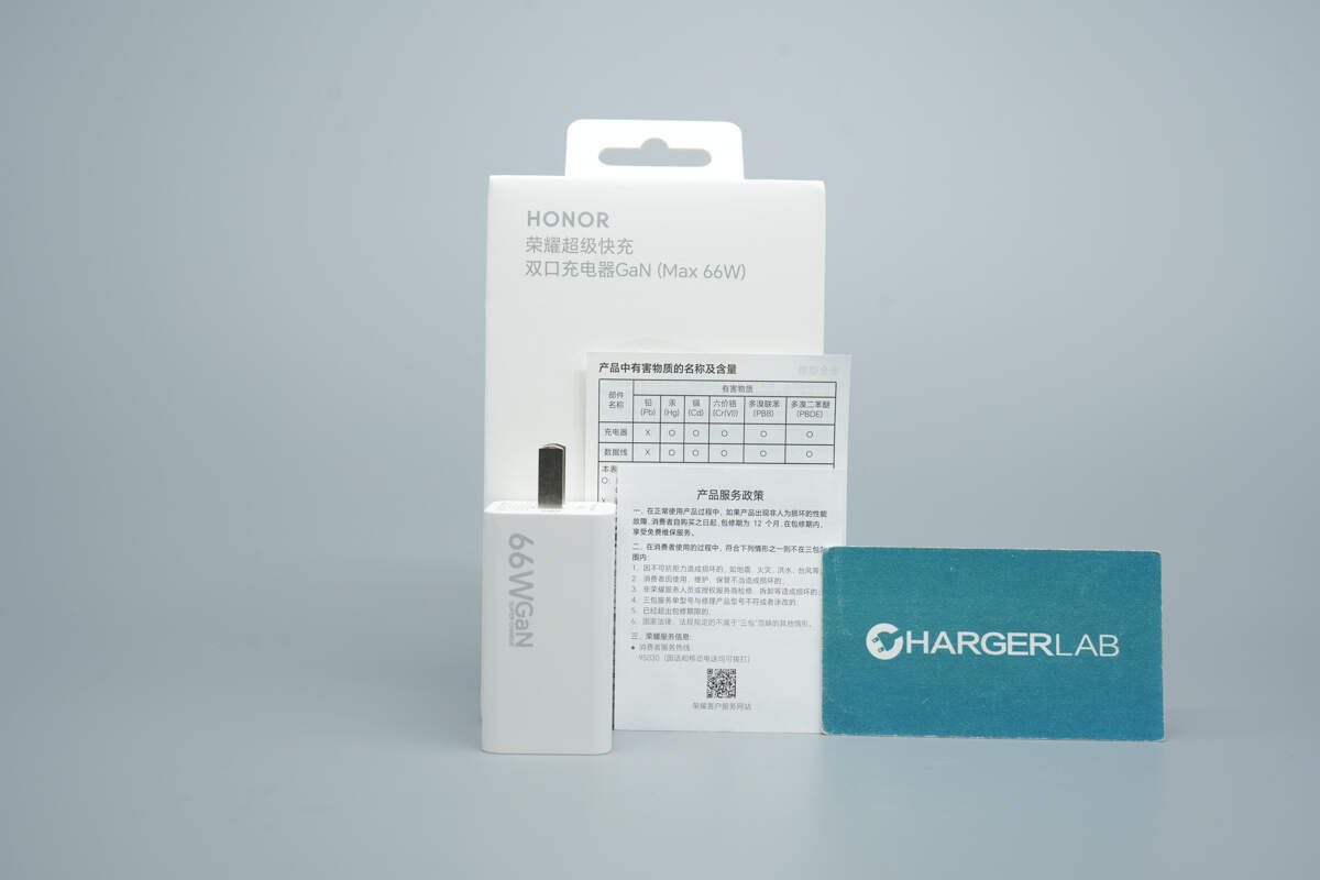
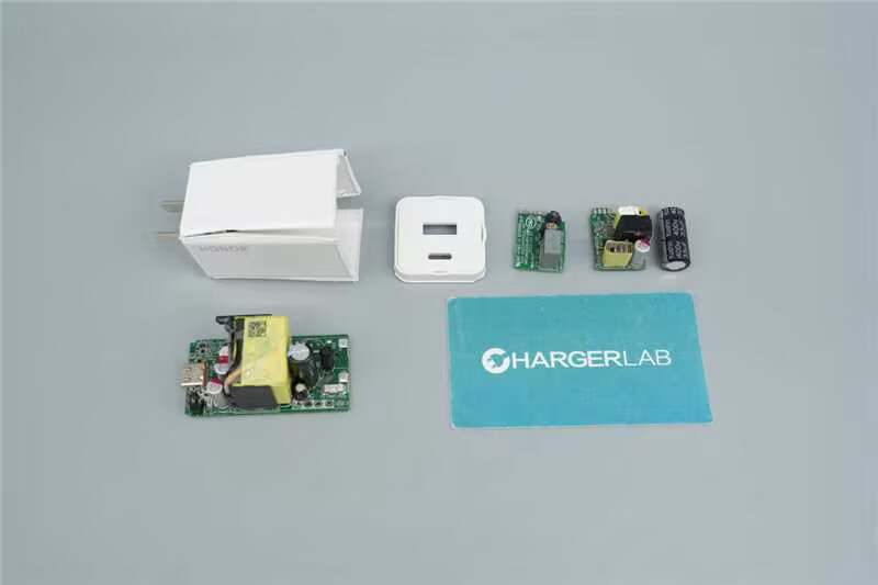
The package includes the charger, a warranty card, and other accompanying materials.
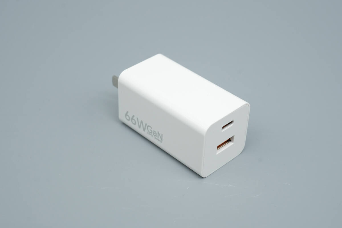
The charger features a white plastic enclosure with a glossy, painted finish, resulting in a smooth surface.
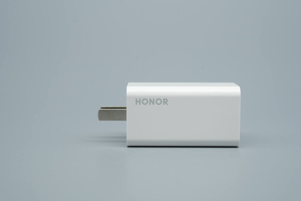
One side is printed with the HONOR logo.
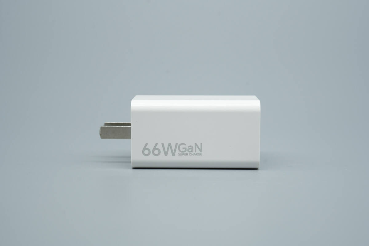
The opposite side is printed with “66W GaN SUPERCHARGE.”
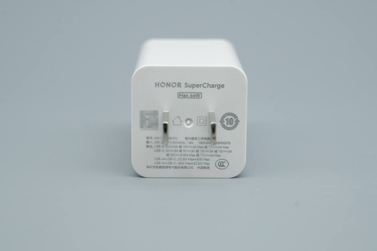
The input-side housing is printed with specs info.
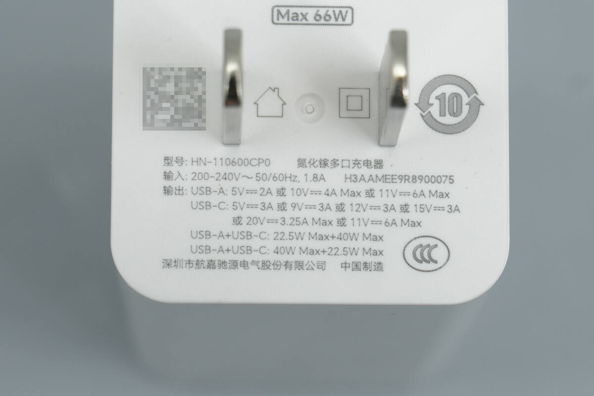
Model: HN-110600CP0
Input: 200–240V~50/60Hz 1.8A
Output:
USB-A: 5V 2A, 10V 4A, 11V 6A Max
USB-C: 5V 3A, 9V 3A, 12V 3A, 15V 3A, 20V 3.25A, 11V 6A
USB-A + USB-C: 22.5W + 40W
USB-A + USB-C: 40W + 22.5W
The charger has obtained CCC certification.
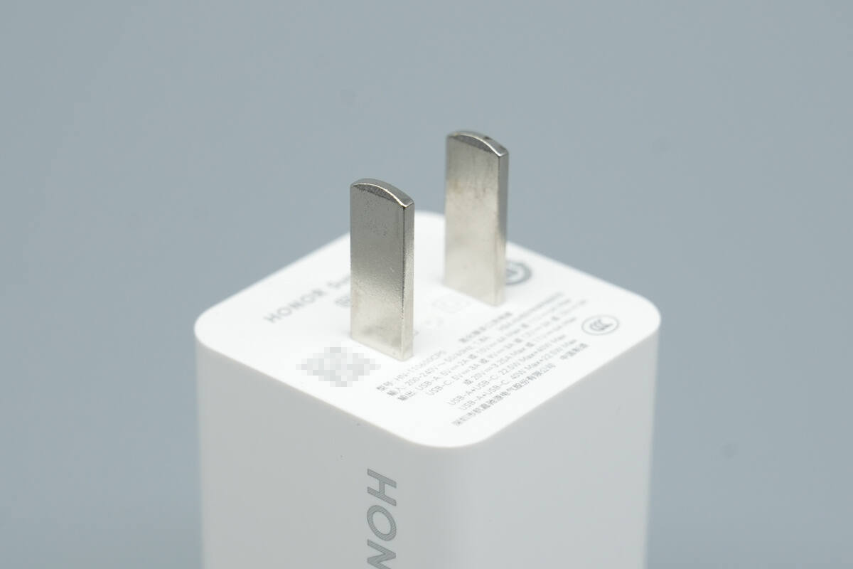
It is equipped with fixed prongs.
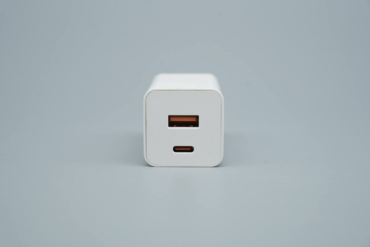
The top features one USB-A port and one USB-C port.
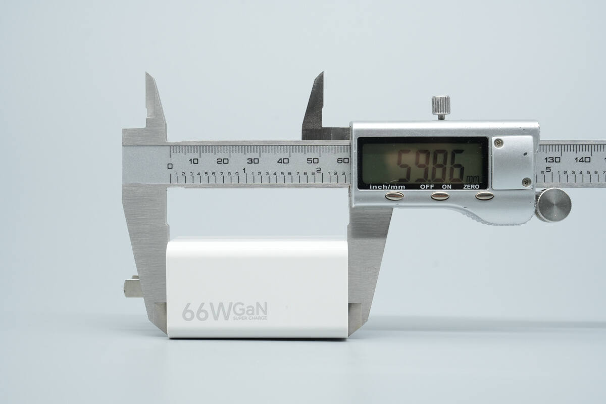
The length of the charger is about 59.86 mm (2.36 inches).
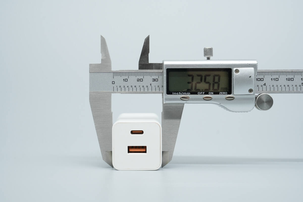
The width is about 32.58 mm (1.28 inches).
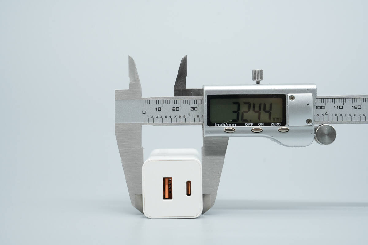
The thickness is about 32.44 mm (1.28 inches).
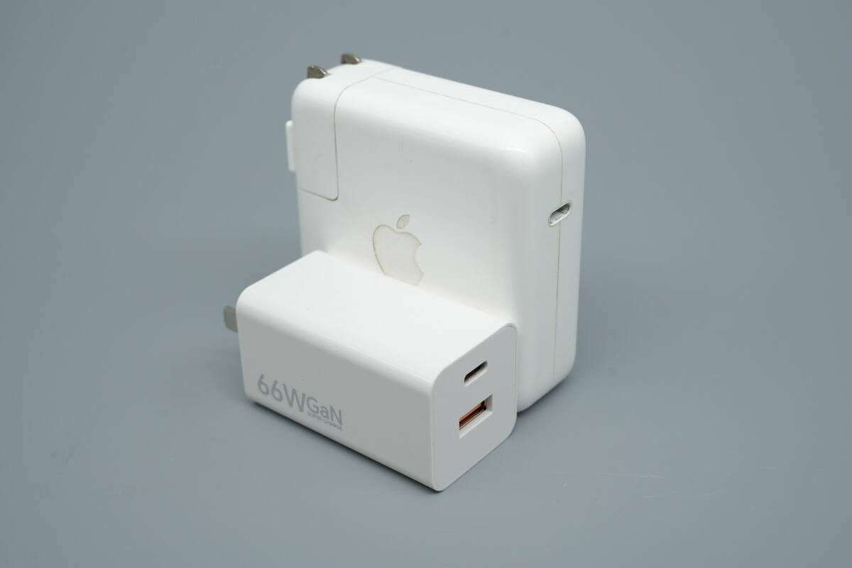
Its size is slightly smaller than that of the Apple 67W charger.
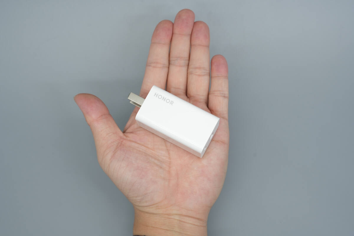
That's how big it is on the hand.

The weight is about 104 g (3.67 oz).
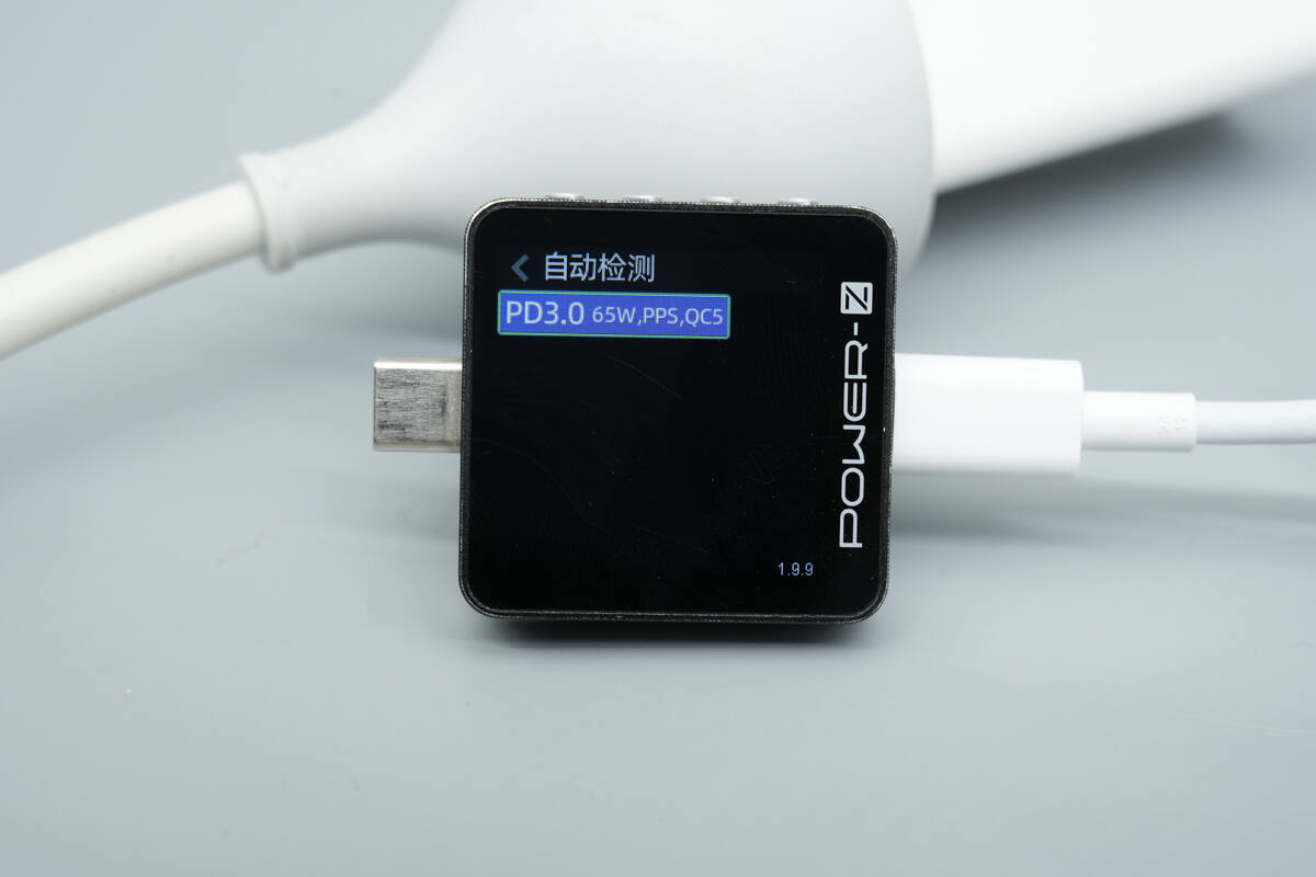
ChargerLAB POWER-Z KM003C shows that the USB-C port supports PD3.0, PPS, and QC5 charging protocols.
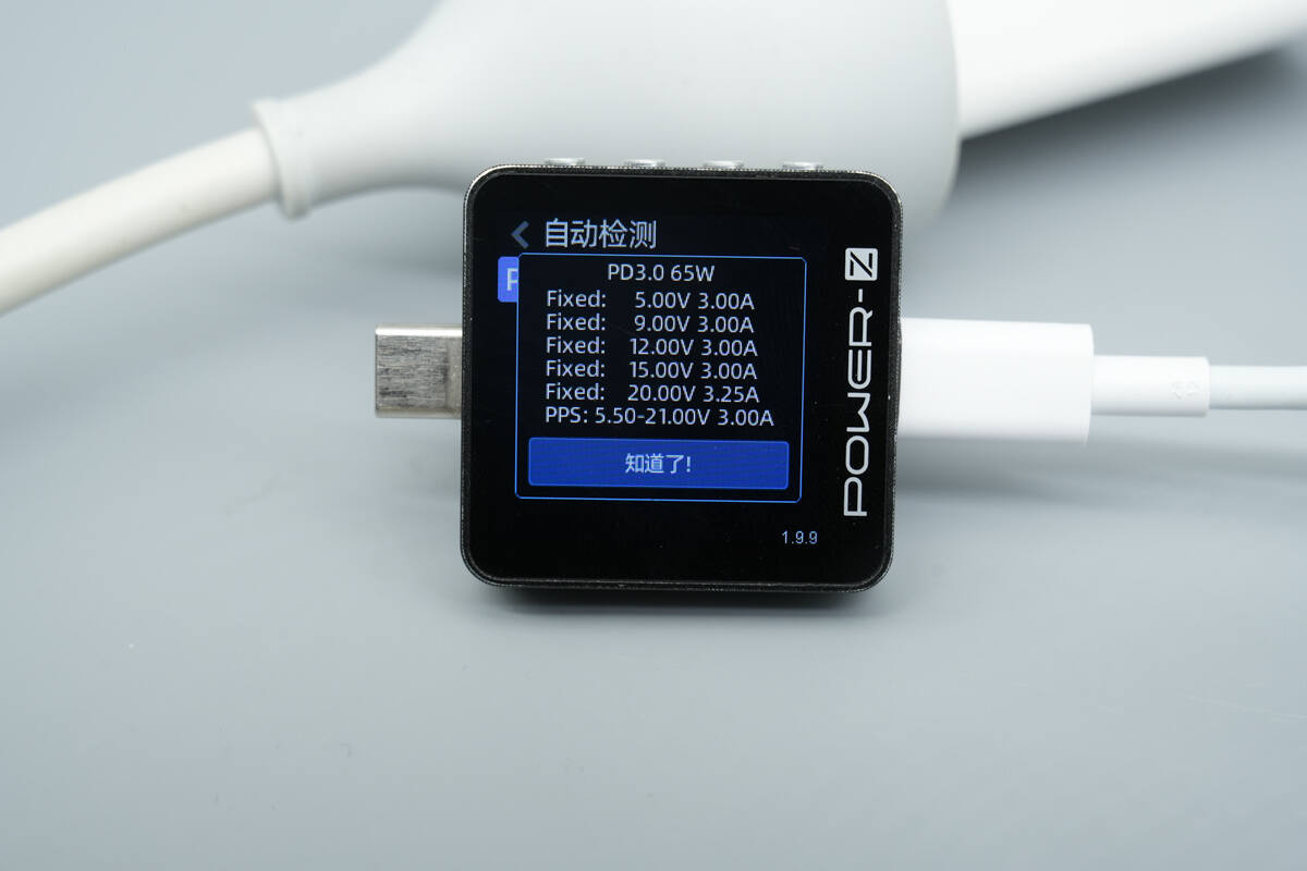
It features five fixed PDOs of 5V3A, 9V3A, 12V3A, 15V3A, and 20V3.25A. It also supports one set of PPS, which is 5-21V3A.
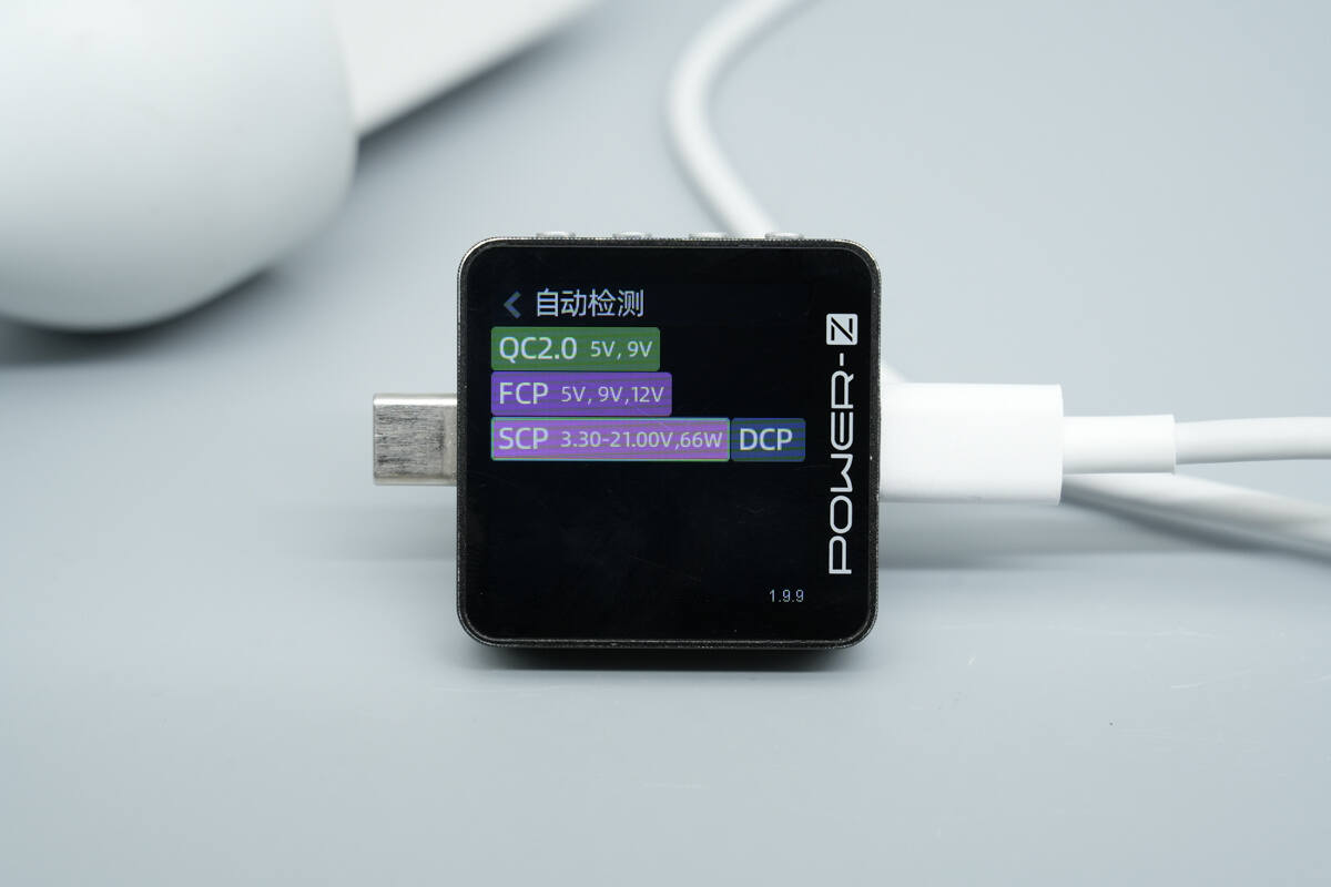
The USB-A port supports QC2.0, FCP, SCP, and DCP charging protocols.
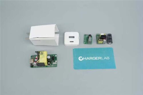
Teardown
Next, let's take it apart to see its internal components and structure.
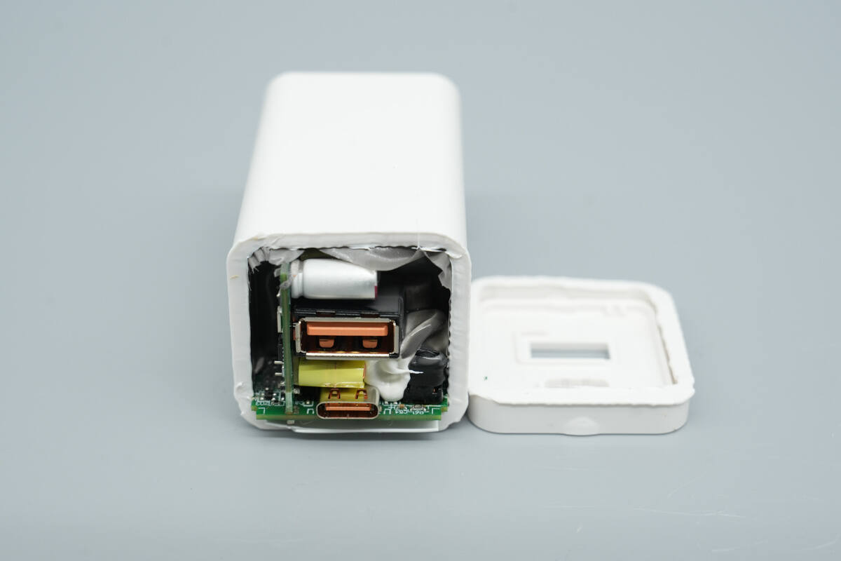
Cutting open the output-side housing reveals that the PCBA module is firmly secured in place.
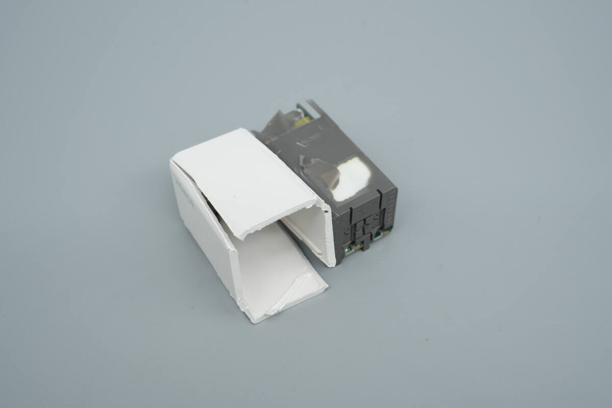
Cut open the housing and remove the PCBA module.
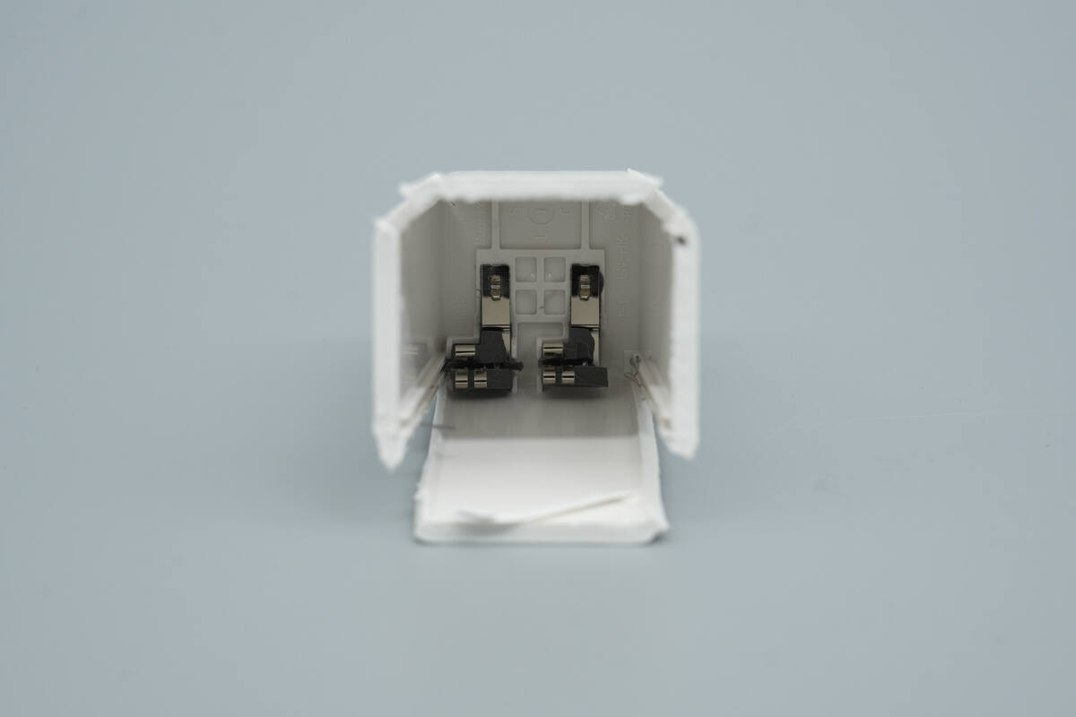
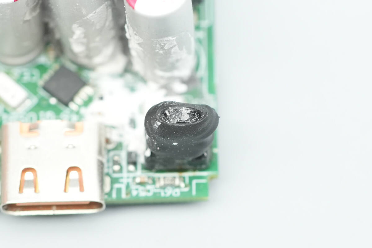
The input side uses a contact-based power connection design, with the prongs crimped to metal plates.
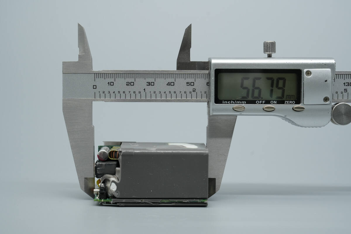
The length of the PCBA module is about 56.79 mm (2.24 inches).
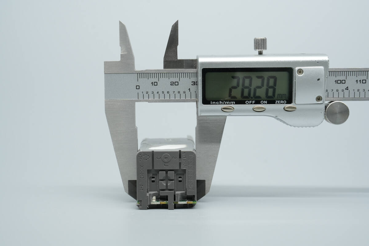
The width is about 28.28 mm (1.11 inches).
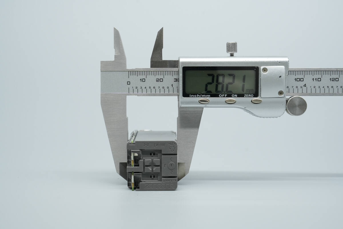
The thickness is about 28.21 mm (1.11 inches).
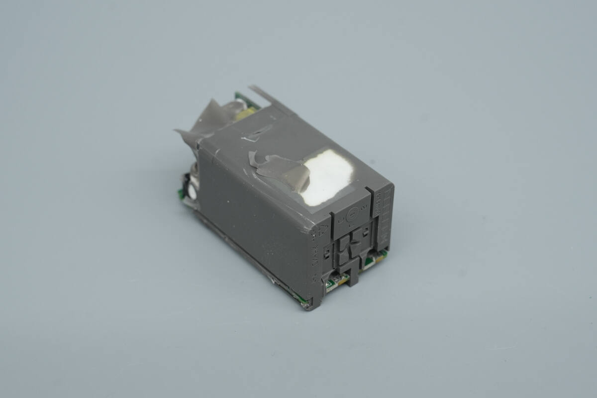
The PCBA module is encapsulated with adhesive to improve overall durability and heat dissipation.
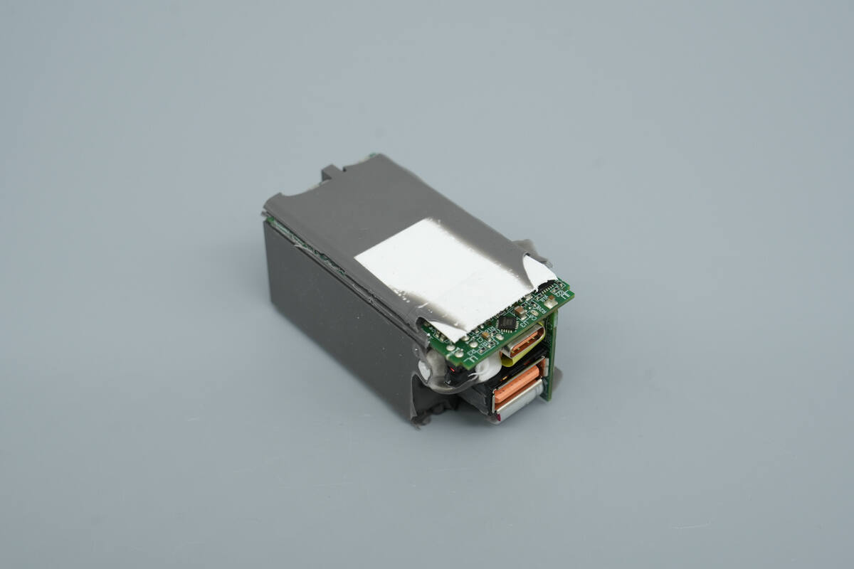
The bottom is covered with a layer of aerogel.

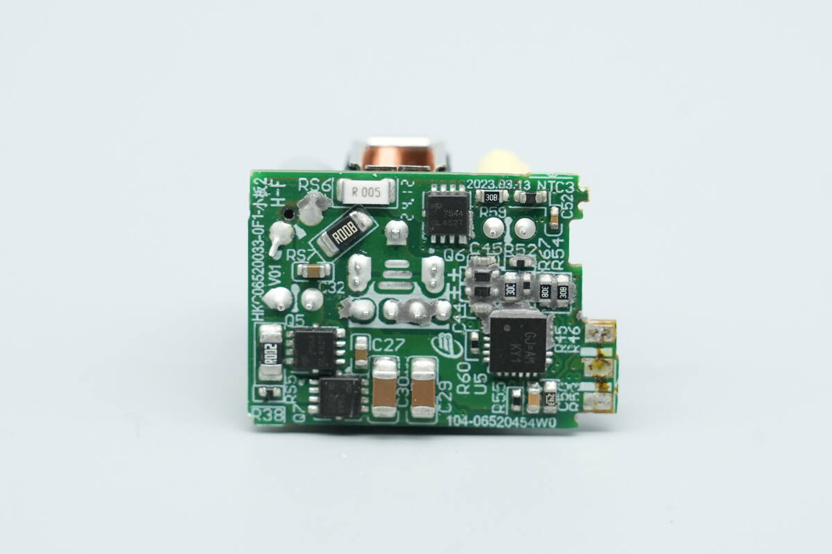
Remove the thermal adhesive. The components on the front of the PCBA module are arranged compactly. Small PCBs are installed at both the input and output ends, and the transformer is insulated with a plastic casing on the secondary side.
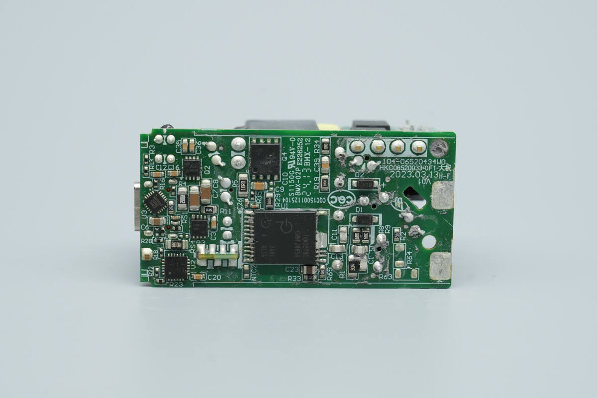
The back side features the master control chip, synchronous rectifier, synchronous buck controller, synchronous buck MOSFETs, and a protocol chip.
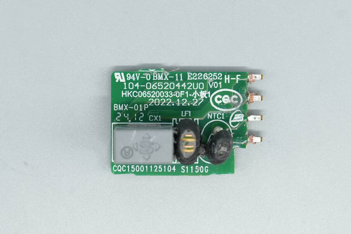
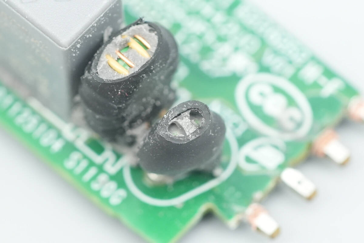
Remove the small PCB on the front left side of the module, revealing an NTC thermistor, a common mode choke, and a safety X2 capacitor on the front.
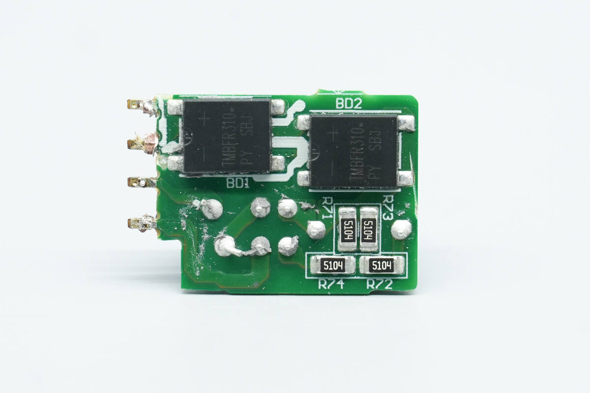
The other side houses two bridge rectifiers.
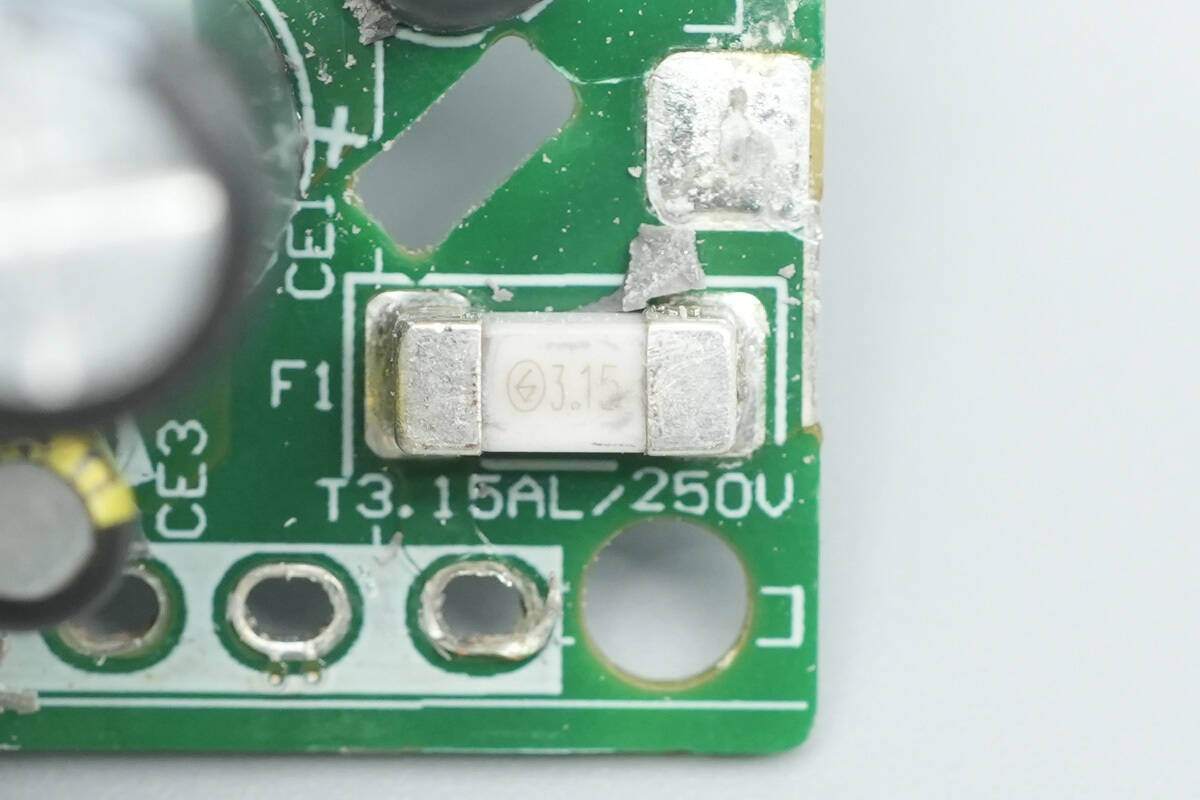
The fuse is from Betterfuse with a rated current of 3.15A.
The NTC thermistor is used to suppress inrush current at power-on and is insulated with a heat-shrink tube.
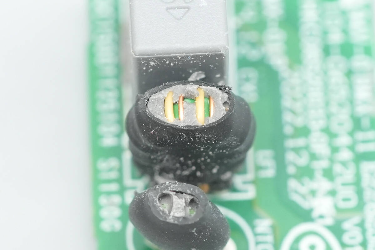
The common mode choke is used to filter EMI and is also covered with a heat-shrink tube.
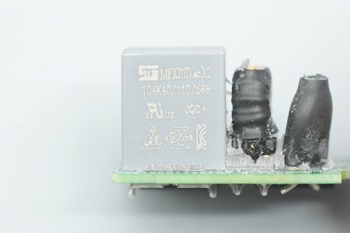
The safety X2 capacitor is from STE with a capacitance of 0.1 μF.
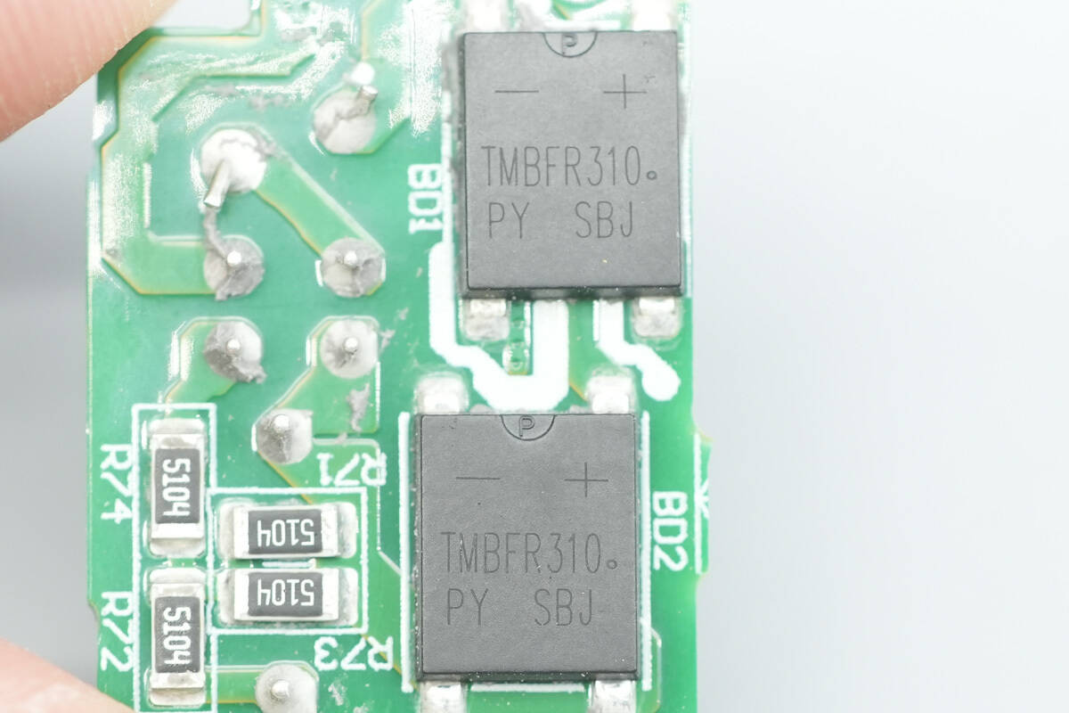
The two bridge rectifiers are from PY, model TMBFR310, rated at 3A 1000V, and use a TMBF package.
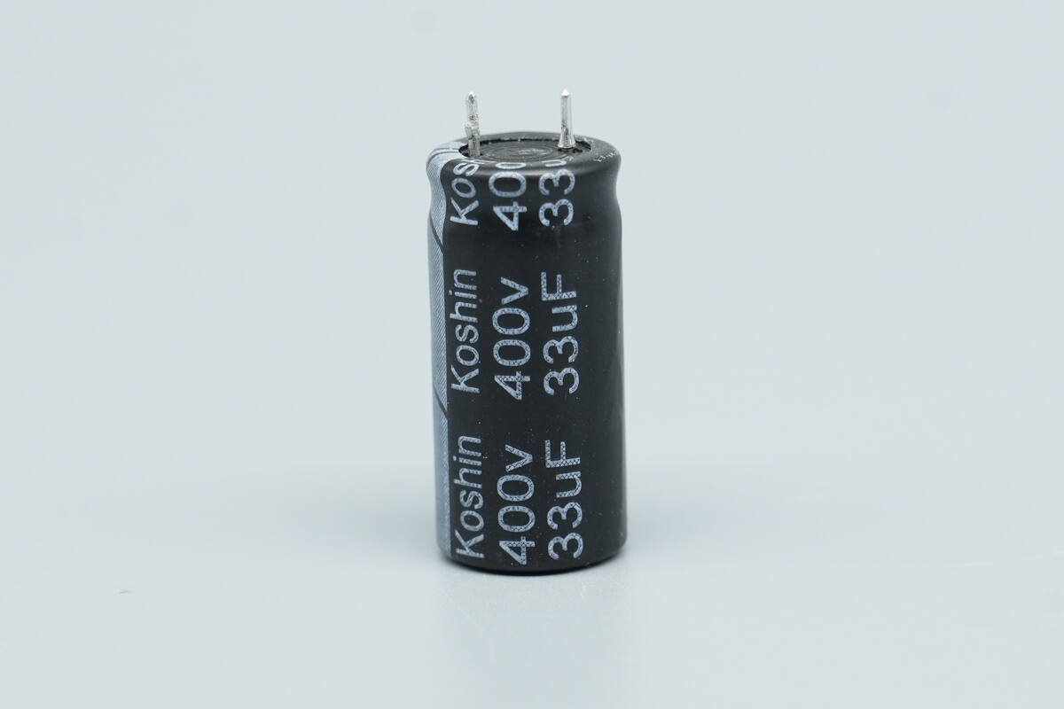
The high-voltage filtering electrolytic capacitor is from Koshin, rated at 400V 33 μF.
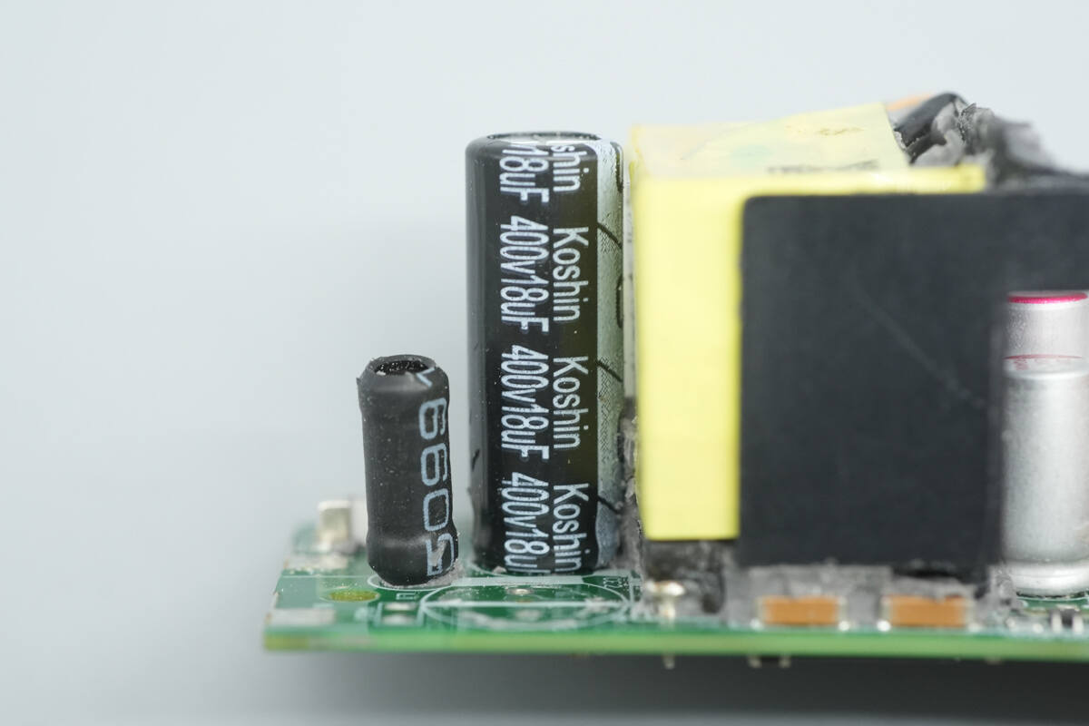
The other high-voltage filtering electrolytic capacitor is also from Koshin, rated at 400V 18 μF.
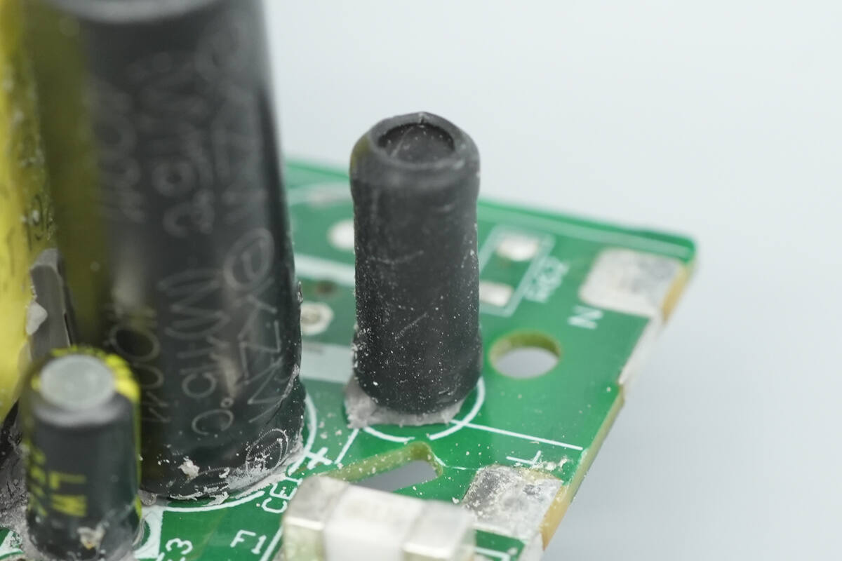
The I-shaped inductor is insulated with a heat-shrink tube.
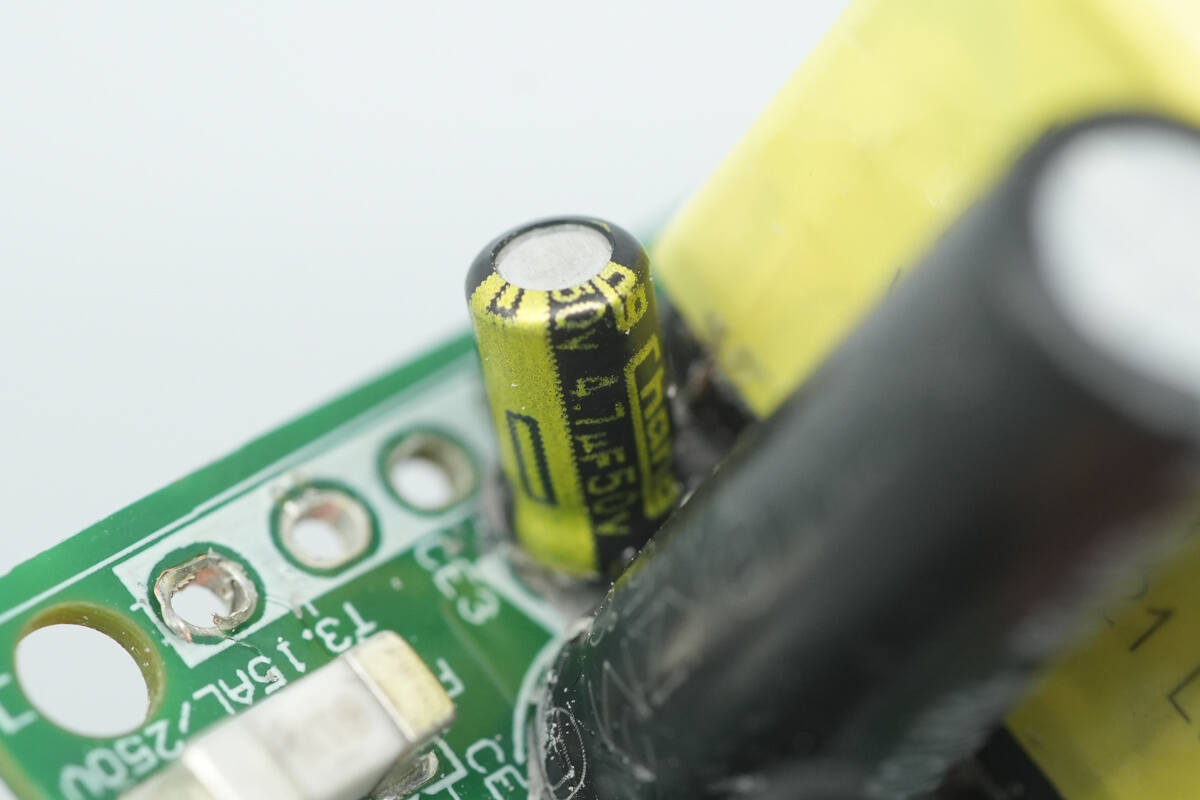
The capacitor supplying power to the master control chip is rated at 50V 4.7 μF.
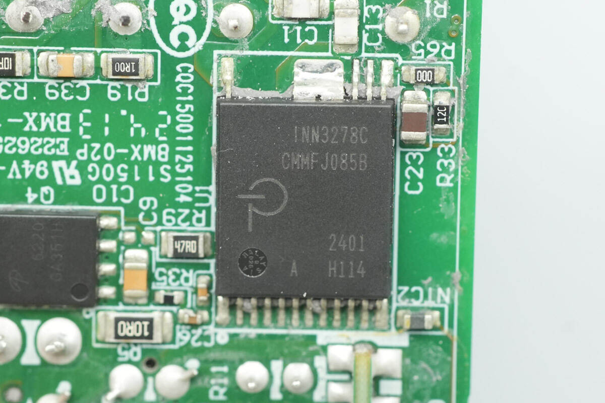
The master control chip is from PI, model INN3278. It is a GaN-based control IC that integrates the primary MOSFET, synchronous rectification controller, feedback, and constant-power characteristics for a quasi-resonant flyback power supply. Internally, it includes a 750V Powi GaN FET, supporting up to 55W output over a wide voltage range in enclosed environments. The chip comes in an InSOP-24D package.
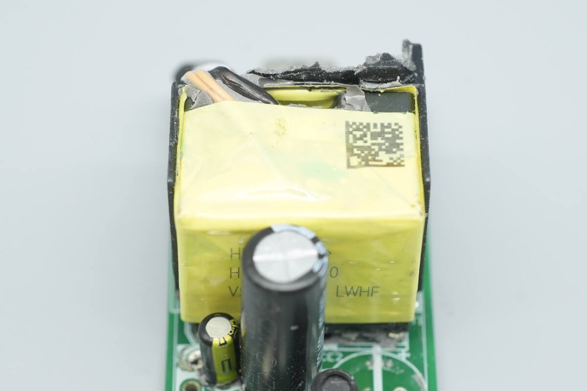
Close-up of the transformer.
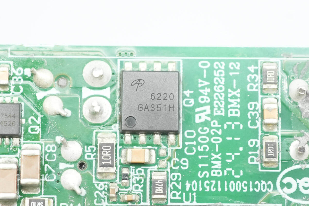
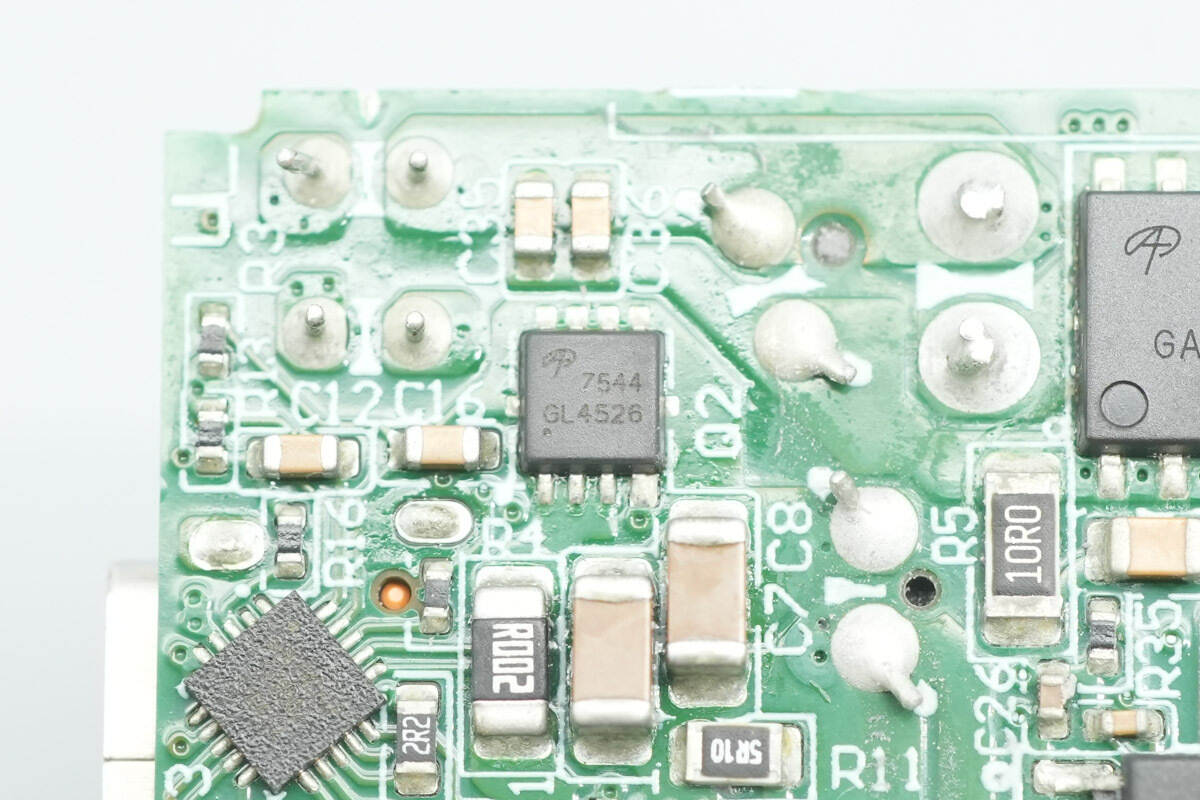
The synchronous rectifier is from AOS, model AON6220. It is an NMOS with a voltage rating of 100 V and an on-resistance of 5.1 mΩ, packaged in a DFN 5×6.
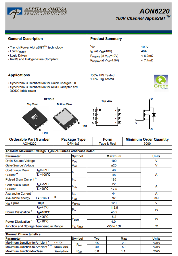
Here is the information about AOS AON6220.

The two solid-state capacitors used for synchronous rectification output filtering are rated at 25 V 470 μF.
Close-up of the filter inductor.

The USB-A socket is soldered onto a small PCB.
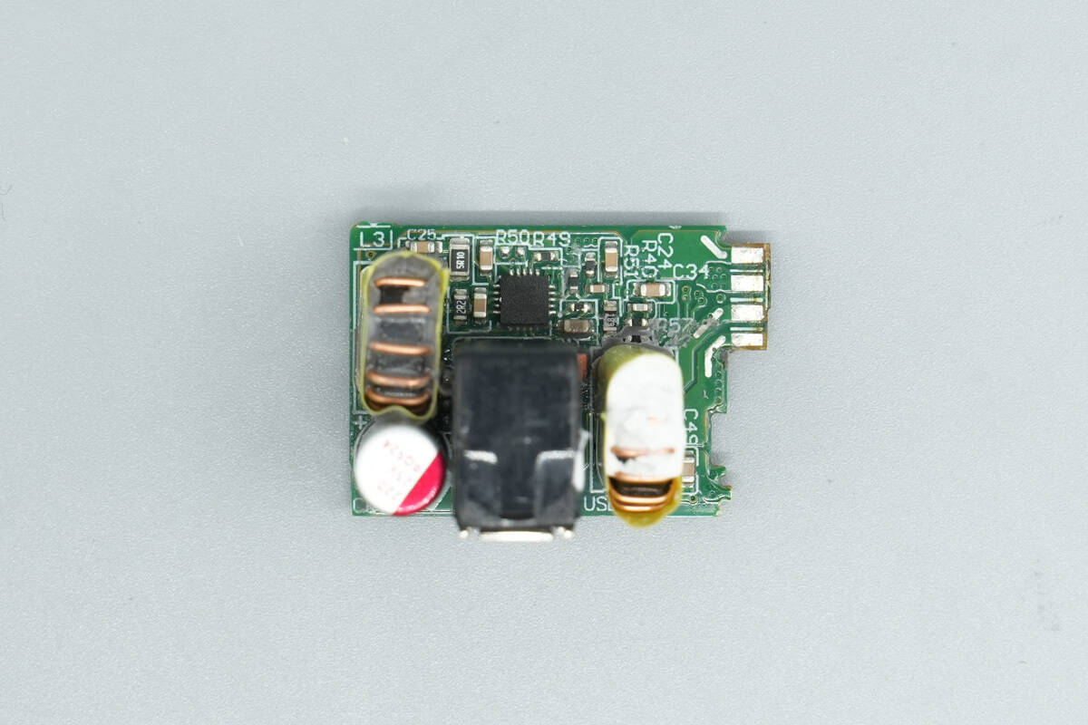
The front of the small PCB houses the synchronous buck controller, buck inductors, and a solid capacitor. The two buck inductors are used for two separate secondary buck circuits.
The other side features the synchronous buck MOSFETs, a protocol chip, and output VBUS MOSFETs.
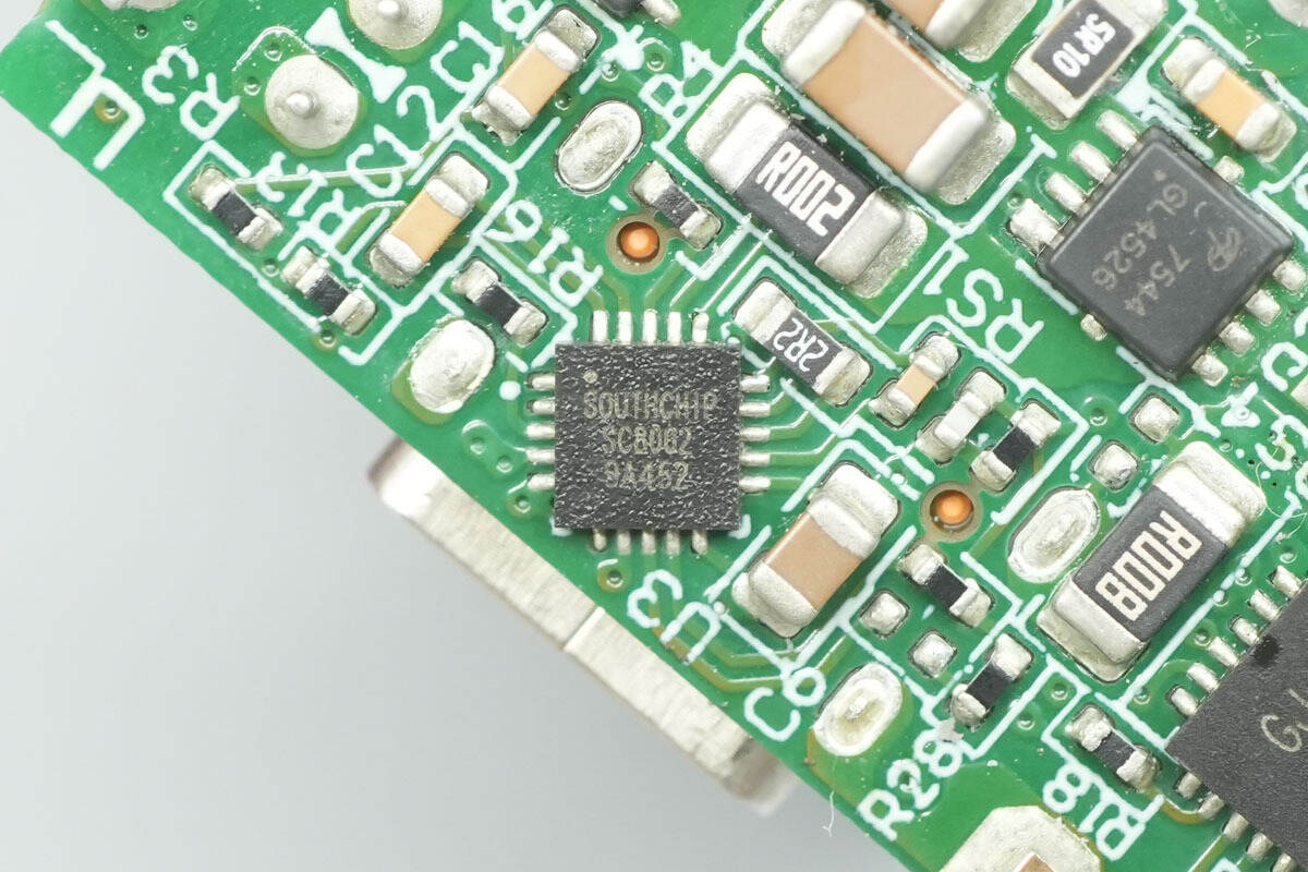
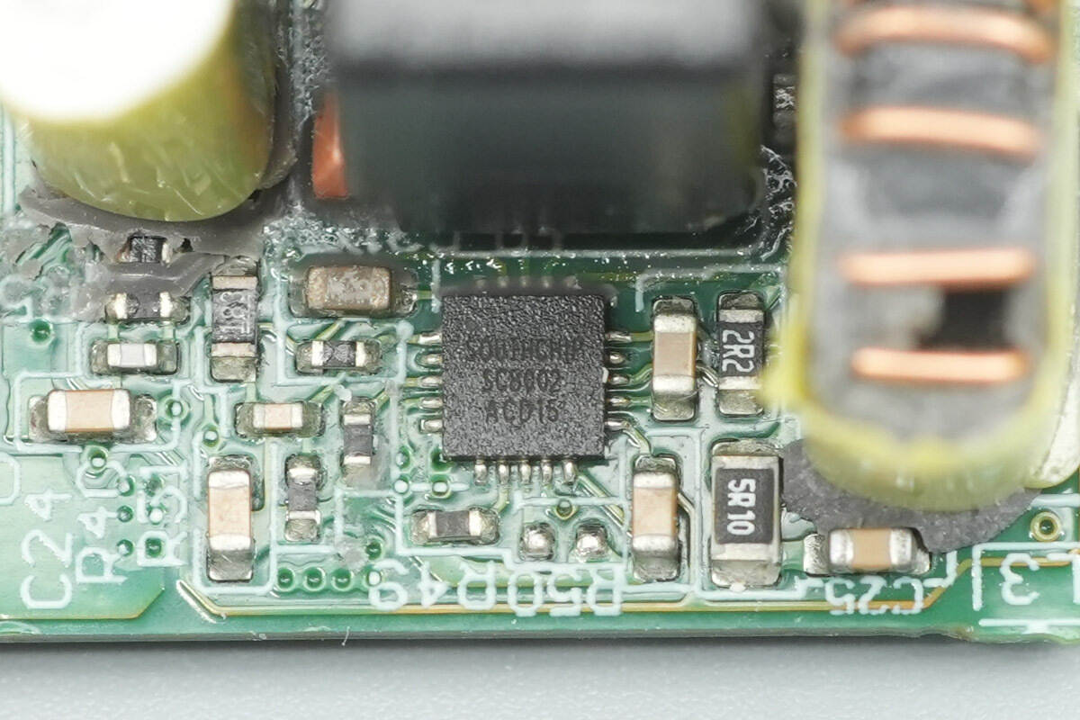
The synchronous buck controller for the USB-C port is from SouthChip, model SC8002. It supports an input voltage range of 4.6–36 V, adjustable output voltage, and a 5 V fixed output for fast-charging applications. The chip features high-precision output current limiting, dual-channel independent current limiting, and comprehensive built-in protection functions. The SC8002 comes in a QFN 3×3-20 package and is suitable for car chargers, multi-port chargers, USB hubs, and similar applications.

Here is the information about SouthChip SC8002.
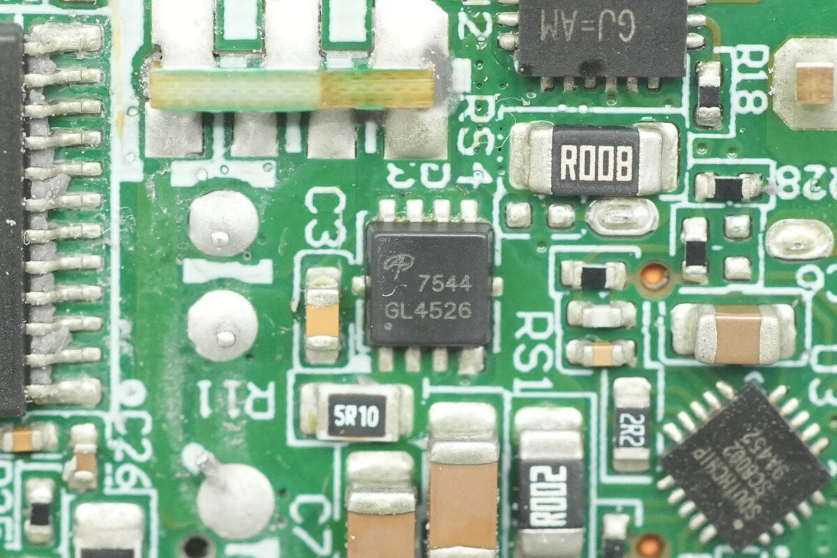
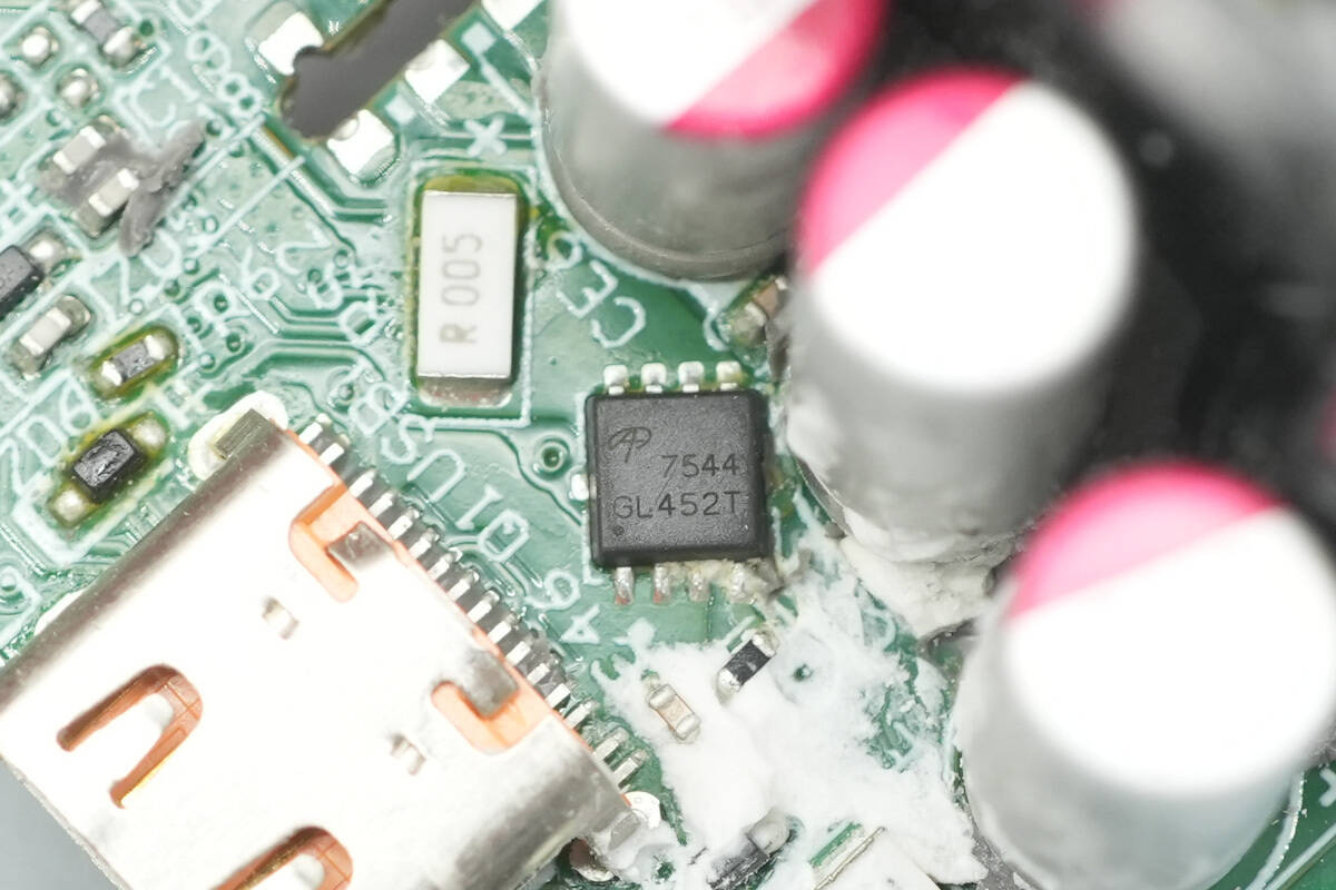
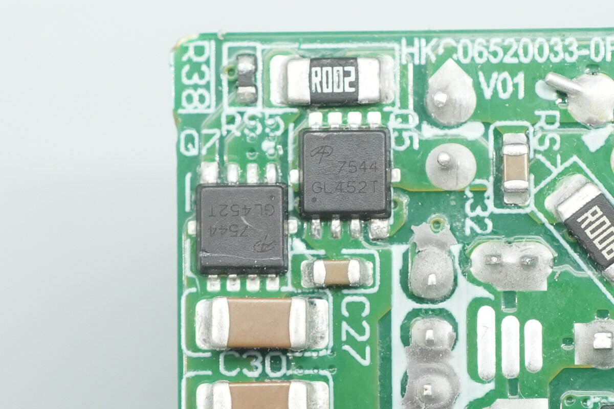
The accompanying synchronous buck MOSFETs and the USB-C output VBUS MOSFETs both use the AOS AON7544. They are NMOS devices rated at 30 V with an on-resistance of 4.1 mΩ, and come in a DFN 3×3 package.

Here is the information about AOS AON7544.
Close-up of the other AOS AON7544 MOSFET.
Close-up of the third MOSFET.

The secondary buck output filtering solid-state capacitor is rated at 25 V 220 μF.
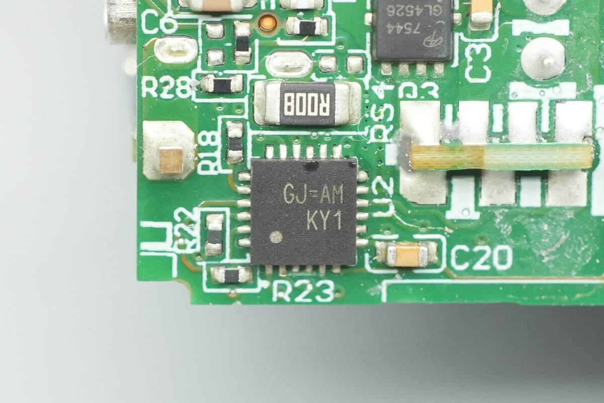
The protocol chip for the USB-C port is marked with “CJ=AM.”
The synchronous buck controller for the USB-A port is also the SouthChip SC8002.
The accompanying synchronous buck MOSFETs are also AOS AON7544.
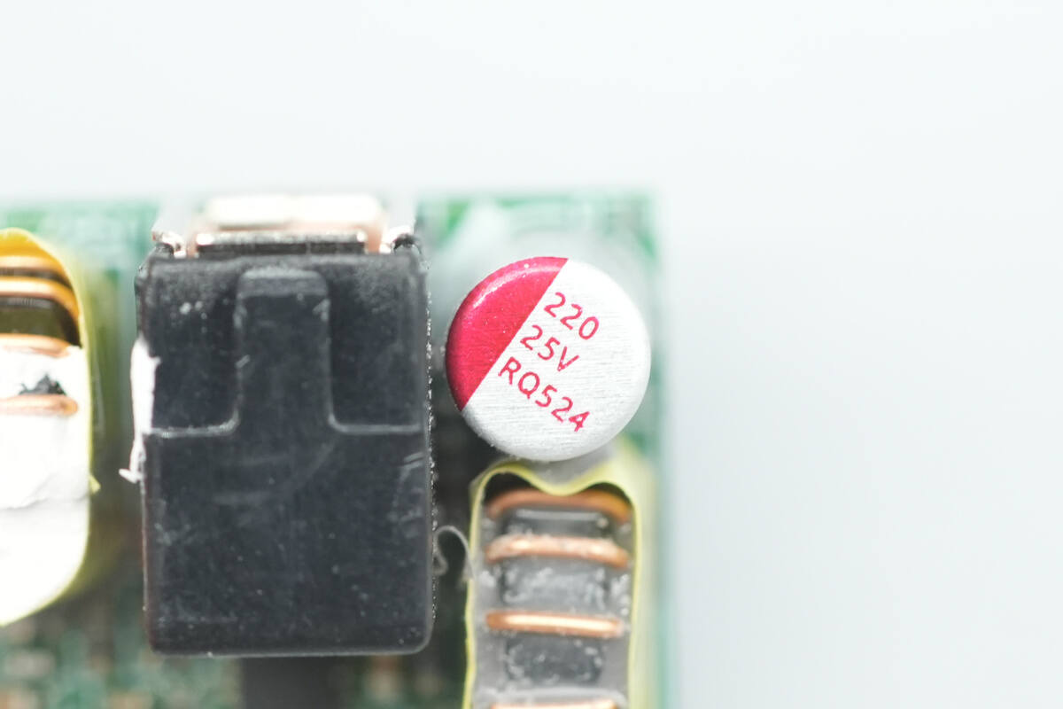
The solid capacitor is rated at 25 V 220 μF.
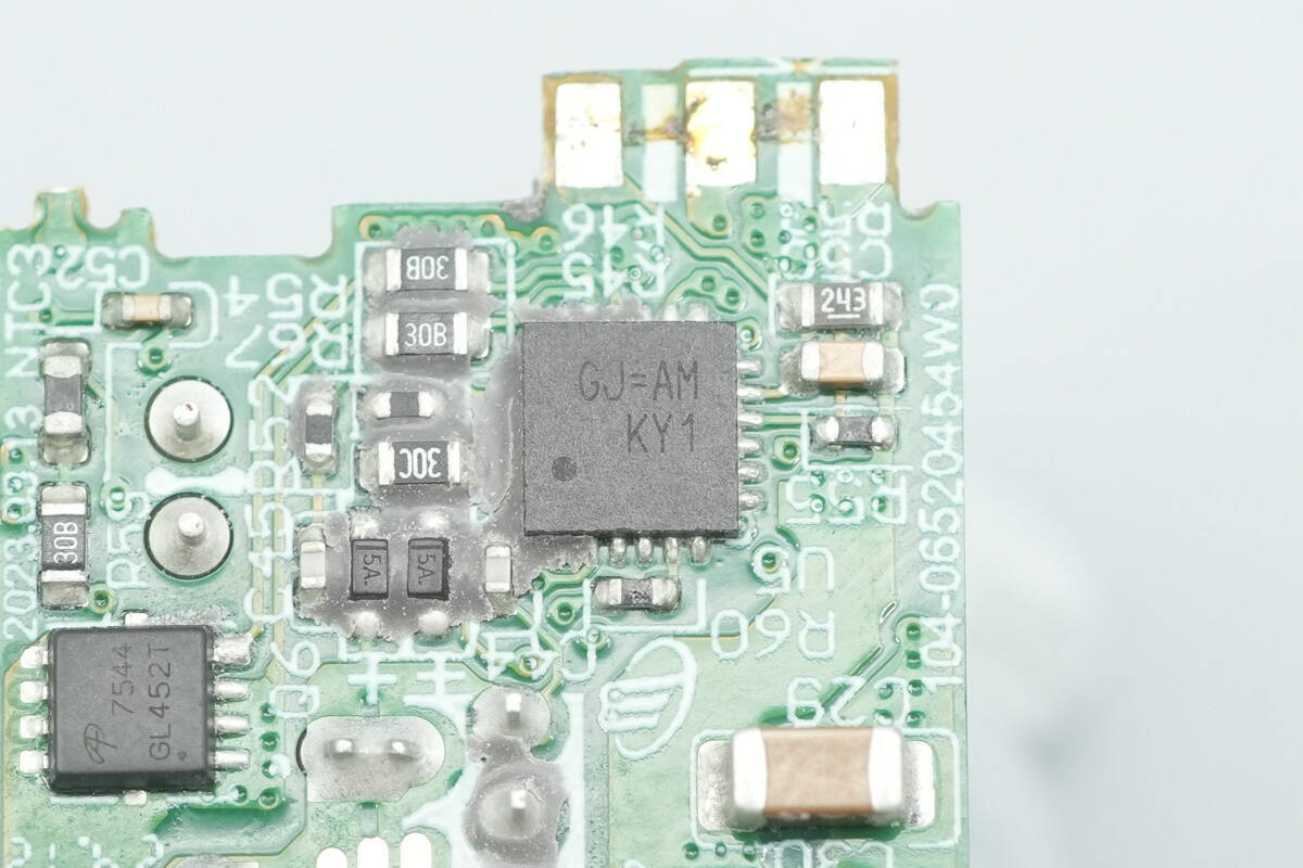
The protocol chip for the USB-A port is the same model as that of the USB-C port.

The output VBUS MOSFET for the USB-A port also uses the AOS AON7544.
Well, those are all components of the HONOR SuperCharge 66W Power Adapter.
Summary of ChargerLAB
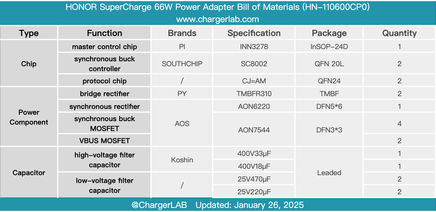
Here is the component list of the HONOR SuperCharge 66W Power Adapter for your convenience.
It is equipped with one USB-A and one USB-C output port, supporting HONOR 66W SuperCharge and 65W PD, respectively. When both ports are used simultaneously, it supports intelligent power distribution of 22.5 W + 40 W or 40 W + 22.5 W.
After taking it apart, we found that the PCBA module has a compact structure, is fully encapsulated with adhesive, and is covered with aerogel to enhance heat dissipation and durability. The power design uses PI’s highly integrated GaN master control chip INN3278, while both secondary-side DC-DC buck circuits use the SouthChip SC8002. All power devices are sourced from AOS.
Overall, the charger not only addresses the limitation of traditional HONOR single USB-A chargers that cannot accommodate laptop charging, but also demonstrates high integration and reliability in its internal components and structure. It truly delivers practical value by enabling one charger for multiple devices with simultaneous fast charging for two devices.
Related Articles:
1. Teardown of Lenovo Thinkplus FLUXO 125W 12800mAh Portable Power Bank (PBFO-12125A)
2. Teardown of DJI Osmo Mobile 8 (DS308)
3. Teardown of Bull 22.5W 10000mAh Semi-Solid State Power Bank (GNV-PGA10EB)