Introduction
Recently, we got our hands on a 100W GaN charger from HONOR. This power adapter is specifically designed for HONOR's lineup of laptops. Compared to traditional chargers, it features a more compact and portable design and comes with a 1.8-meter USB-C cable. It supports not only 100W PD, but also 100W PPS and 127W SCP, meeting the fast charging needs of both HONOR and Huawei devices. Now, let’s take a closer look at the internal design and components.
Product Appearance

The front of the packaging box features the HONOR logo, the product name, and an image of the appearance.

The back of the box displays the selling points and spec information.

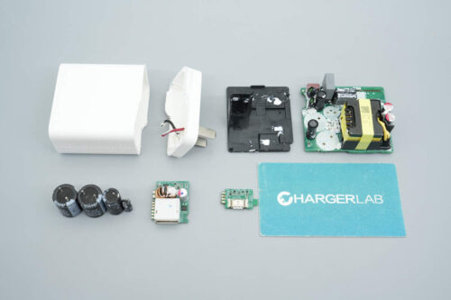
The package includes the charger, cable, and some documents.

The included dual USB-C cable supports up to 5A current.

The length of the cable is about 1.8 m (5.9 feet).

The ChargerLAB POWER-Z KM003C indicates that the cable has an E-Marker chip, supports power delivery of 20V/5A, and has data transfer capability of USB 2.0.

The casing is made of flame-retardant PC material with a glossy surface, featuring a minimalist design.

Both sides are designed with recessed areas to make plugging and unplugging easier.

The input end of the casing is printed with the specification information.

Model: HN-200500CP0
Input: 100-240V\~50/60Hz 2.5A
Output: 5V 3A, 9V 3A, 12V 5A, 15V 5A, 20V 5A
Certified by CCC.

It is equipped with a fixed plug.

There is a USB-C port on the top, marked with “100W” and “HONOR SuperCharge.”

The height of the charger is about 65.25 mm (2.57 inches).

The width is about 65.08 mm (2.56 inches).

The thickness is about 28.61 mm (1.13 inches).

That's how big it is in the hand.

The weight is about 220 g (7.76 oz).

ChargerLAB POWER-Z KM003C shows that it supports SCP, PD3.0, PPS, QC5, and DCP charging protocols.

And it has five fixed PDOs of 5V3A, 9V3A, 12V5A, 15V5A, and 20V5A. It has one set of PPS, which is 3.3-21V5A.

When used to charge the Huawei Pura 80 Pro+, the power is about 95W.
Teardown
Next, let's take it apart to see its internal components and structure.

Cut open the casing and take out the PCBA module.

The length of the PCBA module is about 60.54 mm (2.38 inches).

The width is about 60.72 mm (2.39 inches).

The thickness is about 24.34 mm (0.96 inches).

The PCBA module is potted with adhesive to enhance weather resistance and heat dissipation. A metal heat sink is placed on top for additional cooling.

The bottom is also covered with a metal heat sink, and both heat sinks are lined with insulating tape.

After removing the heat sink, an integrated Mylar sheet is found on the inner side, providing insulation and isolation.

After cleaning off the thermal adhesive, the component layout is revealed to be compact. The transformer is reinforced and insulated with a plastic casing.

On the back side, there are components including the PFC MOSFET, PFC rectifier, master control chip, primary MOSFET, synchronous rectifier controller, synchronous rectifiers, optocouplers, and SMD Y capacitors.

At the front end of the PCBA module, from left to right, the components include: time-delay fuse, varistor, NTC thermistor, common mode chokes, safety X2 capacitor, bridge rectifier, film capacitors, and filter inductor.

The time-delay fuse is from Betterfuse, with part number 932 and rated at 3.15A 250V.

The varistor is from JOYIN, marked with 10S681K, and is used for surge overvoltage absorption.

The NTC thermistor is used to suppress inrush current when the power is turned on.

The common mode choke features dual-wire winding and is used to filter out EMI interference.

The safety X2 capacitor is from HJC, with a capacitance of 0.22 μF.

Close-up of the secondary common mode choke.

The bridge rectifier is from Pingwei, model D4KBR10, rated at 4A 1000V, and uses a D3K package.

Both film capacitors have specifications of 1μF 450V.

Close-up of filter inductor.

On this side, there is a PFC boost inductor and an electrolytic capacitor, with the capacitor covered by a plastic sleeve.

The PFC boost controller is marked with 3CC and identified as the Onsemi NCP1622. It is an enhanced CrM boost PFC controller, featuring valley frequency foldback, improved transient response, and higher conversion efficiency, while requiring fewer external components. The NCP1622 performs power factor correction on the pulsating DC output from the bridge rectifier to supply power to the switching power supply.

The PFC boost MOSFET uses the Navitas GaNFast power chip NV6136A, a highly integrated GaN power device. It features a built-in driver and a high-precision, lossless current-sensing circuit, eliminating the losses associated with sampling resistors. The NV6136A integrates a 170mΩ Rds(on), 700V GaN FET, supports switching frequencies up to 2MHz, and comes in a compact 6×8mm QFN package, saving board space.

Close-up of the PFC boost inductor.

The PFC rectifier is marked with MUR4JGR, which is an ultrafast recovery diode in an SMC package.

The high-voltage filter electrolytic capacitor is from AiSHi.

It has a specification of 420V and 82μF.

A high-voltage filter electrolytic capacitor in the center area is protected by a plastic sleeve.

It is also from AiSHi.

Its specification is 420V 10μF.

On the other side of the module, there are blue Y capacitors and solid capacitors used for output filtering.

A small PCB to the right of the transformer has the USB-C socket soldered onto it.

The master control chip is the Onsemi NCP1342, a high-frequency quasi-resonant flyback primary PWM controller. It features built-in high-voltage startup, active X2 capacitor discharge, supports a wide range of Vcc supply voltages, and allows an external thermistor connection for over-temperature protection along with multiple comprehensive protection functions.

The primary MOSFET uses the Navitas NV6134A, which features a built-in driver and a high-precision, lossless current-sensing circuit. It has an on-resistance of 260mΩ, a voltage rating of 650V, supports switching frequencies up to 2MHz, and comes in a compact 6×8mm QFN package to save board space.

The capacitor supplying power to the master control chip is from BERYL, with a specification of 160V 10μF.

Close-up of the transformer.

The HK1018 optocoupler is used for output voltage feedback.

Close-up of another HK1018 optocoupler.

The SMD Y capacitors are from TRX, with part number TMY1331K. Their small size and lightweight design make them well-suited for high-density power products such as GaN fast chargers.

Close-up of two blue Y capacitors.

The synchronous rectifier controller is from MPS, marked with IBHJ, model MP6908A, with a maximum operating frequency of 600kHz. It supports multiple operating modes, including DCM, CCM, QR, and ACF, works for both high-side and low-side applications, features ringing detection to prevent false turn-on, and supports both logic-level and standard-voltage synchronous rectifiers.

The synchronous rectifiers are from AOS, model AONS62922. They are NMOS transistors with a voltage rating of 120V and an on-resistance of 5.8mΩ, housed in a DFN 5×6 package.

Here is the information about AOS AONS62922.

The two solid capacitors for output filtering are from BERYL, both rated at 25V 680μF.

On the front side of the output PCB, there is a VBUS MOSFET installed. The USB-C socket is reinforced with a steel sleeve.

On the back side, there is a protocol chip installed.

The protocol chip is from Weltrend, model WT6651P, and it supports Qualcomm QC5 fast charging.

The VBUS MOSFET is from AOS, model AONR36366. It is an NMOS transistor with a voltage rating of 30V and an on-resistance of 2.8mΩ, housed in a DFN 3×3EP package.

Here is the information about AOS AONR36366.

Close-up of the USB-C socket.

Well, those are all components of the HONOR 100W GaN Charger.
Summary of ChargerLAB

Here is the component list of the HONOR 100W GaN Charger for your convenience.
It continues the classic design style, featuring a USB-C port, and comes with a 1.8-meter cable to suit most usage scenarios. Designed with a GaN-based solution, it is compact and portable. It supports PD3.0/PPS 100W and 127W SCP fast charging, meeting the fast-charging needs of devices ranging from laptops and tablets to smartphones.
After taking it apart, we found that it is designed based on a PFC + QR flyback topology, using the Onsemi NCP1622 PFC controller, NCP1342 master control chip, and MPS MP6908A synchronous rectifier controller. It is paired with two GaN devices from Navitas — the NV6136A and NV6134A — as well as AOS AONS62922 synchronous rectifiers.
The output voltage is controlled by a Weltrend protocol chip. High-quality capacitors from two well-known brands, AiSHi and BERYL, are used. The module is potted for enhanced durability, and components such as the transformer and capacitors are reinforced and insulated. Overall, the materials and build quality are reliable.
Related Articles:
1. Teardown of UGREEN Nexode 65W Charger with Retractable USB-C Cable (X605)
2. Teardown of UGREEN USB-C to DisplayPort 8K Cable (CM556)
3. Teardown of CANDYSIGN 160W CoCan Ultra