Introduction
We recently received the Highsay C1 Pro 140W Ultra Charger, which features three USB-C ports and one USB-A port. Both USB-C1 and USB-C2 support up to 140W PD 3.1, while USB-C3 supports 30W PD. The USB-A port delivers 22.5W SCP, making it capable of simultaneously charging the entire Apple ecosystem, with a maximum total output of 140W.
This Highsay model also comes with a smart display, providing real-time information on each port’s power, total power, and temperature, ensuring safer and more reliable use. Here’s a closer look at this product.
Product Appearance
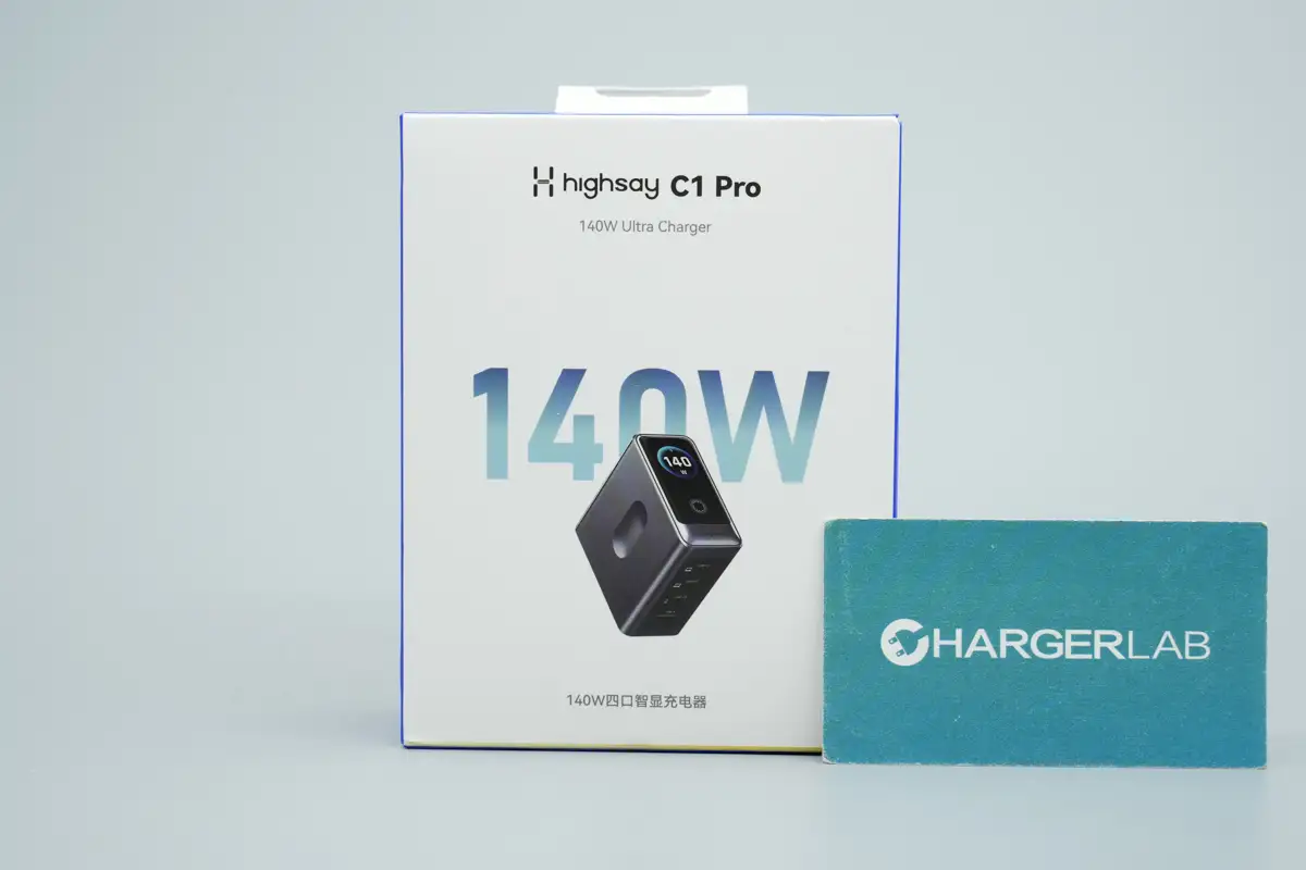
The front of the packaging box displays the brand, product name, and an image of the charger.
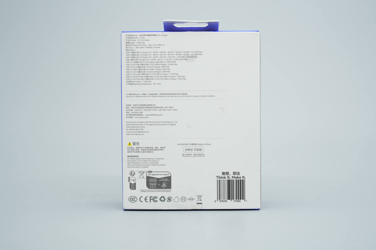
The back of the packaging is printed with product specifications, manufacturer information, precautions, and relevant certifications.
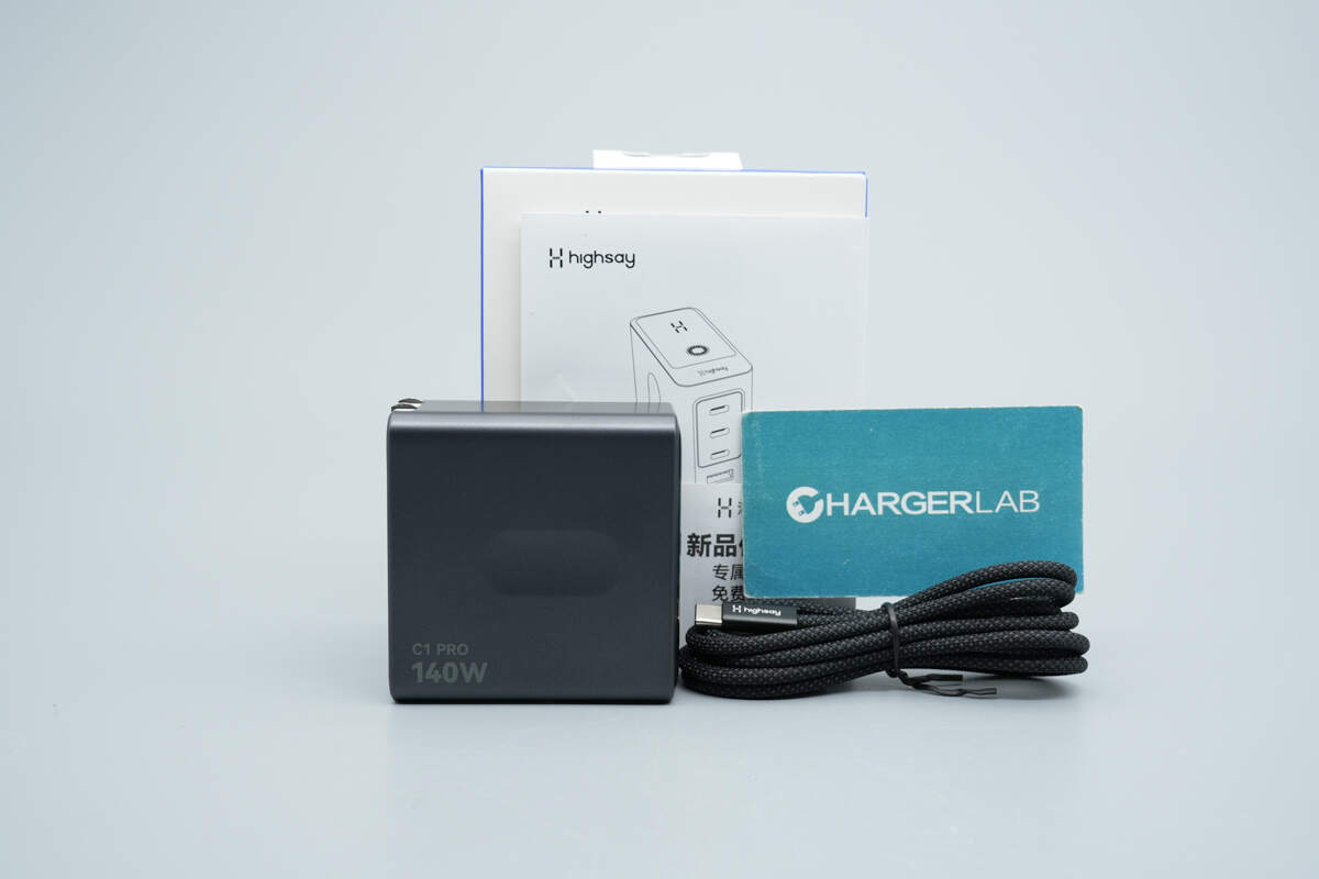
Inside the package are the charger, a charging cable, and a user manual.
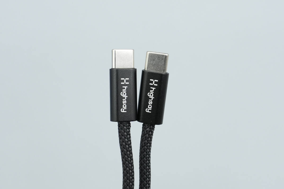
The included USB-C braided cable features the Highsay logo on the connector housing.
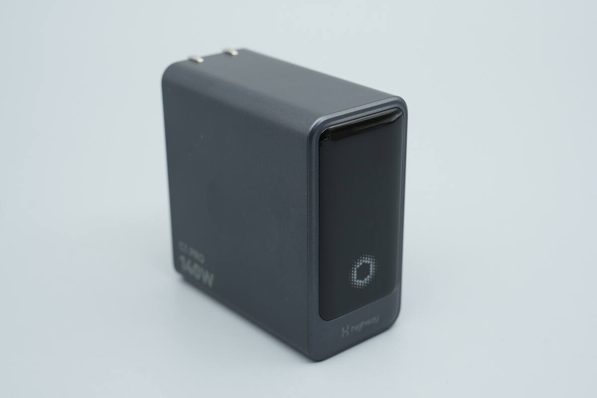
The housing is made of flame-retardant PC material with a painted surface, giving it a deep, refined finish and a solid, premium feel.
There are small recessed grooves on both sides of the body, making it easier to plug in and unplug.
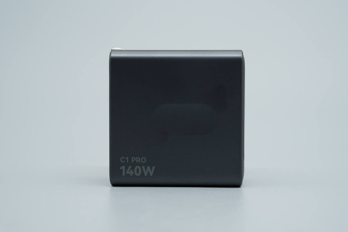
The front is marked with “C1 PRO” and “140W.”
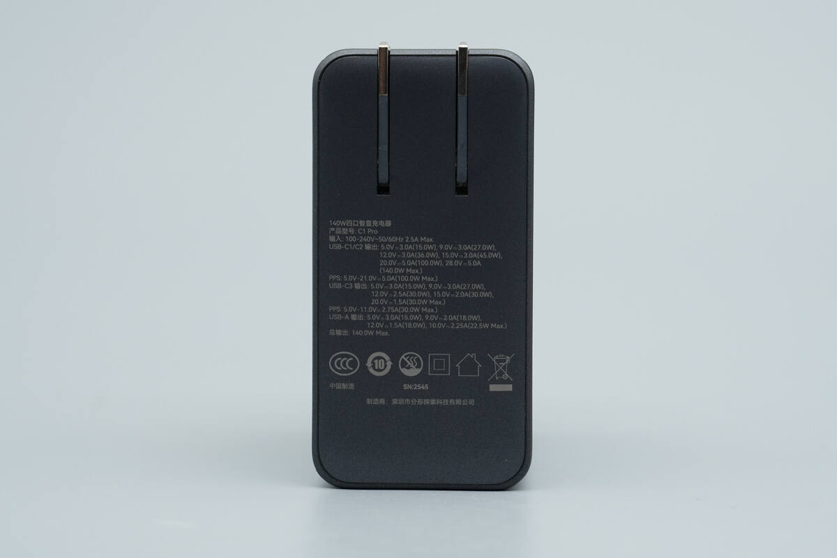
The input-side housing is printed with the specification information.
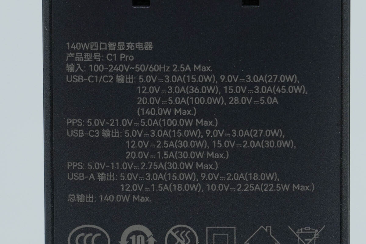
Model: C1 Pro
Input: 100–240V~ 50/60Hz, 2.5A Max
Output:
USB-C1/C2: 5V 3A, 9V 3A, 12V 3A, 15V 3A, 20V 5A, 28V 5A (140W Max)
PPS: 5V–21V 5A (100W Max)
USB-C3: 5V 3A, 9V 3A, 12V 2.5A, 15V 2A, 20V 1.5A
PPS: 5–11V 2.75A (30W Max)
USB-A: 5V 3A, 9V 2A, 12V 1.5A, 10V 2.25A (22.5W Max)
Total Output: 140W Max
The product has passed CCC certification.
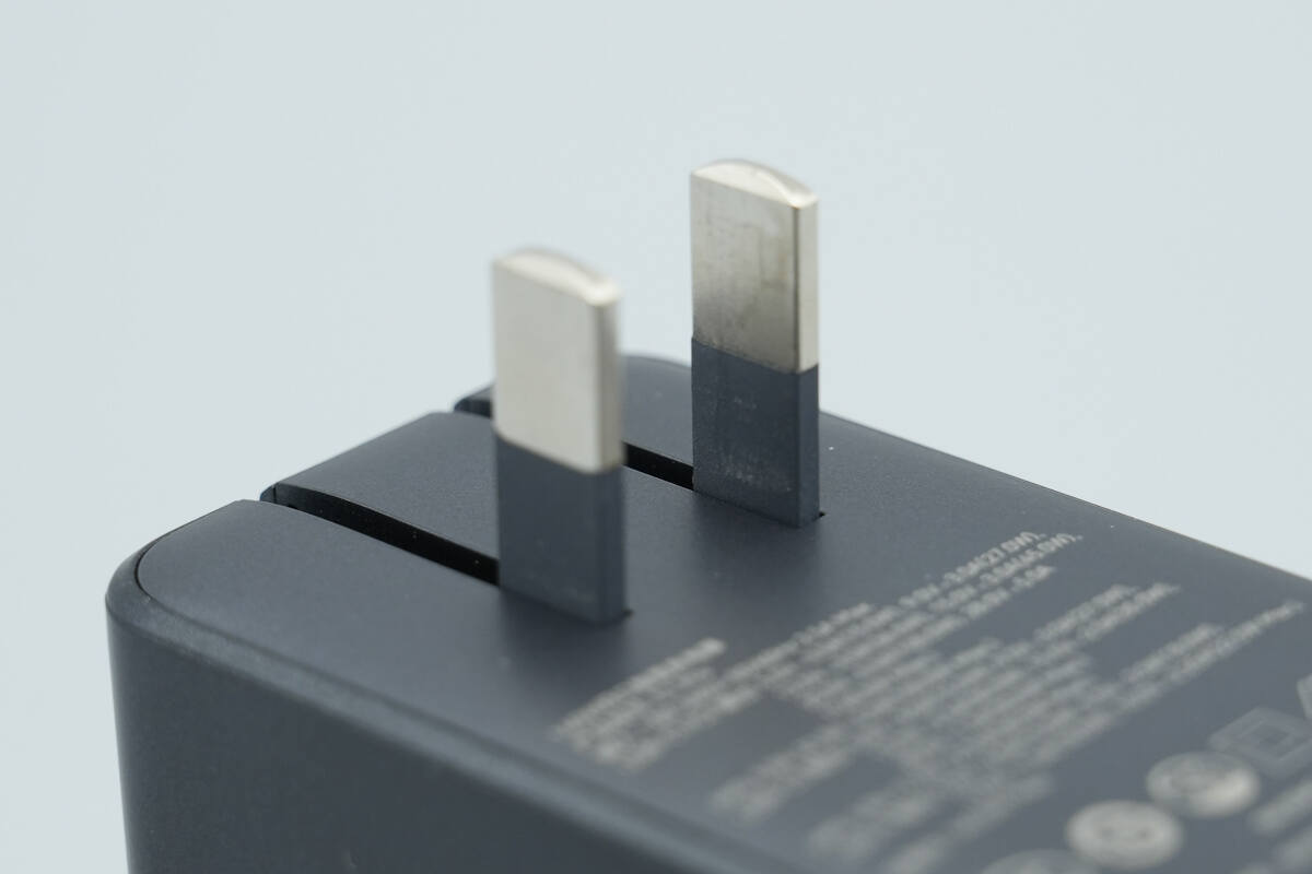
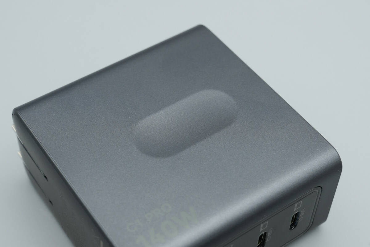
It is equipped with foldable prongs.
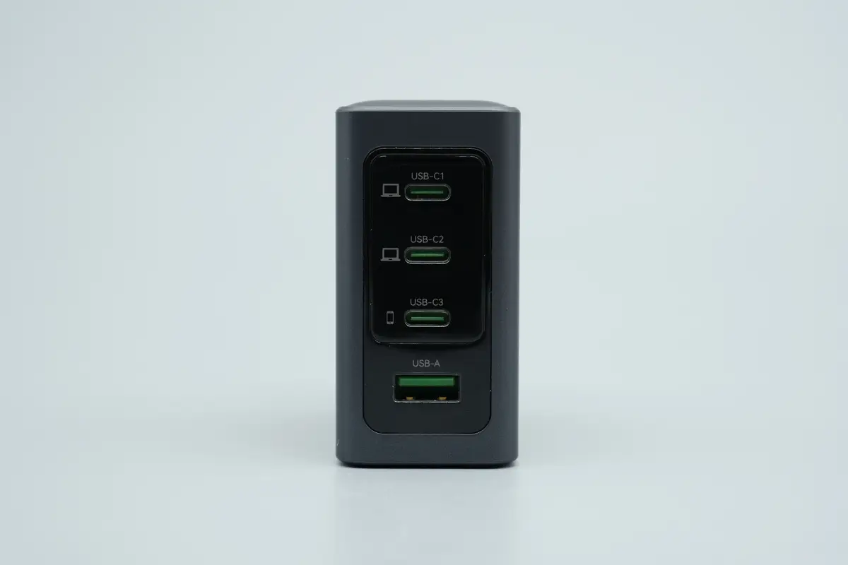
The output side features three USB-C ports and one USB-A port.
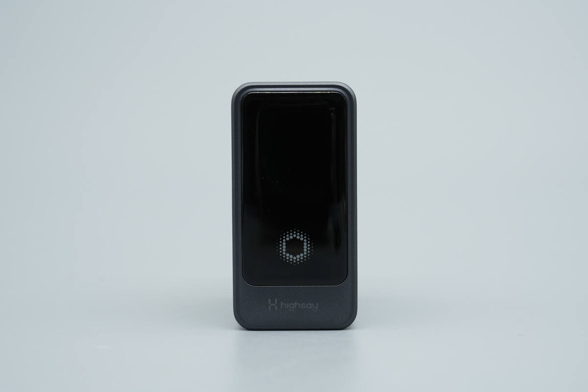
The top of the body is equipped with a smart display and a touch-sensitive button.
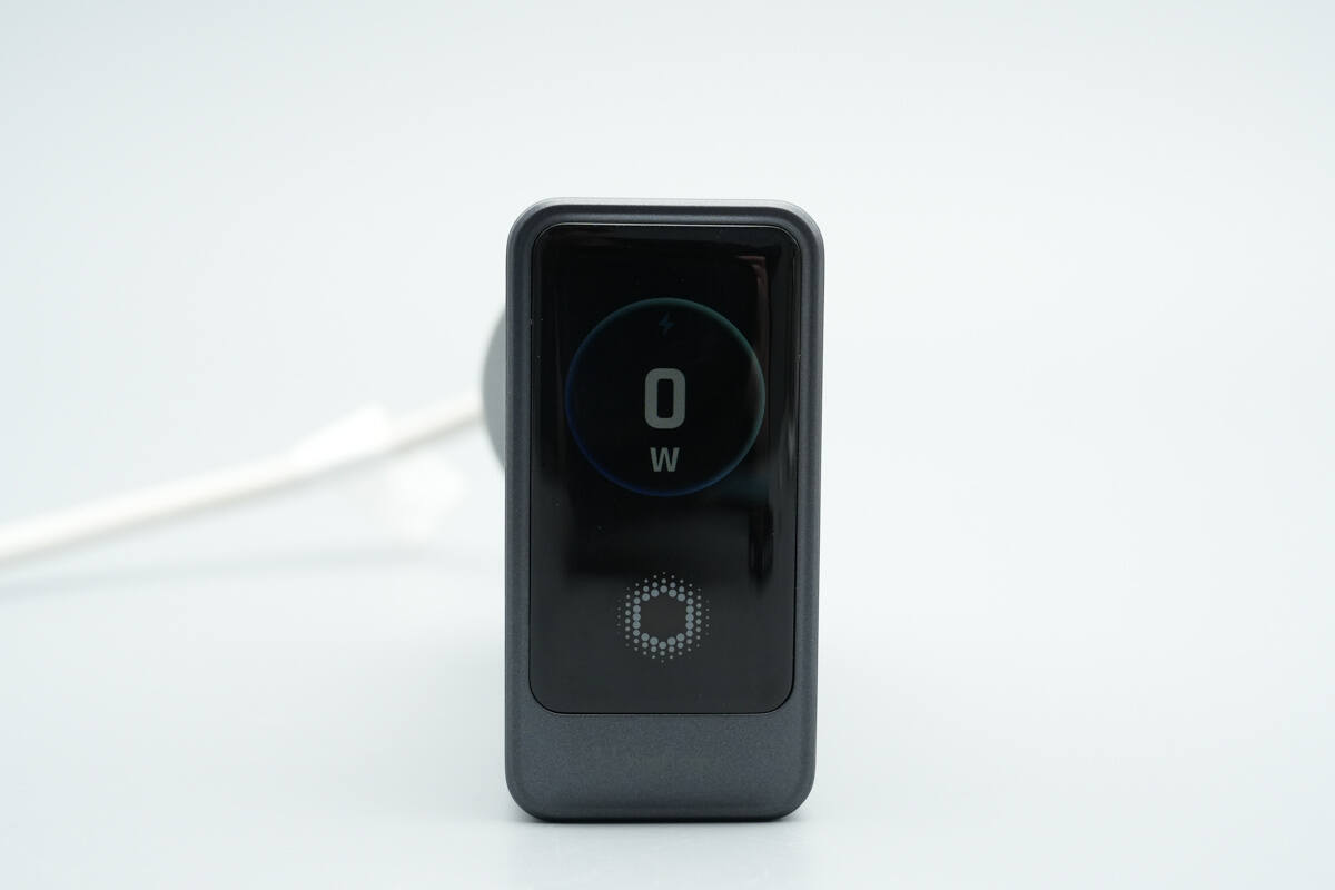
The digital display can switch interfaces via the touch button and is currently showing the total output power interface.
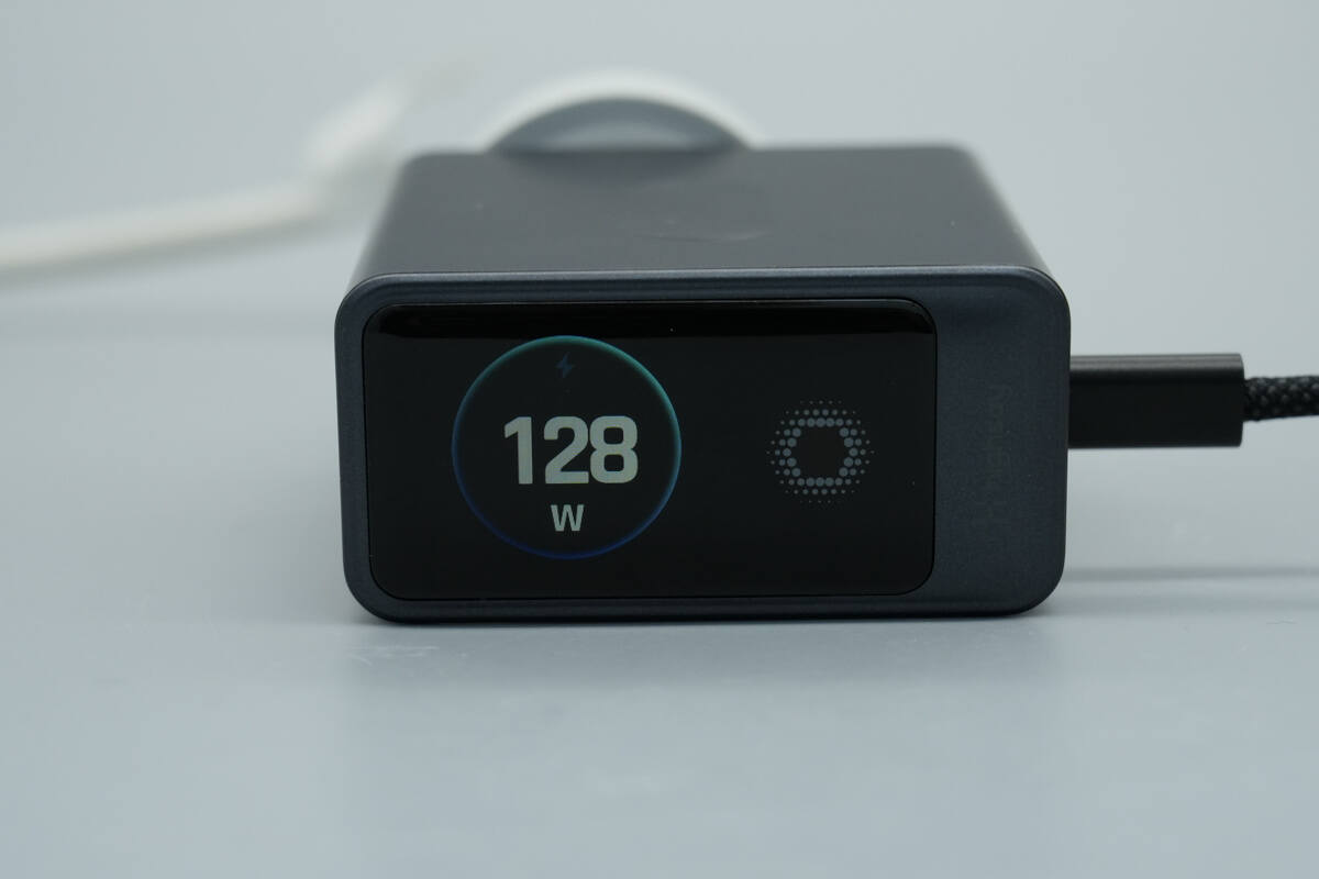
The interface can also be switched between landscape and portrait modes.
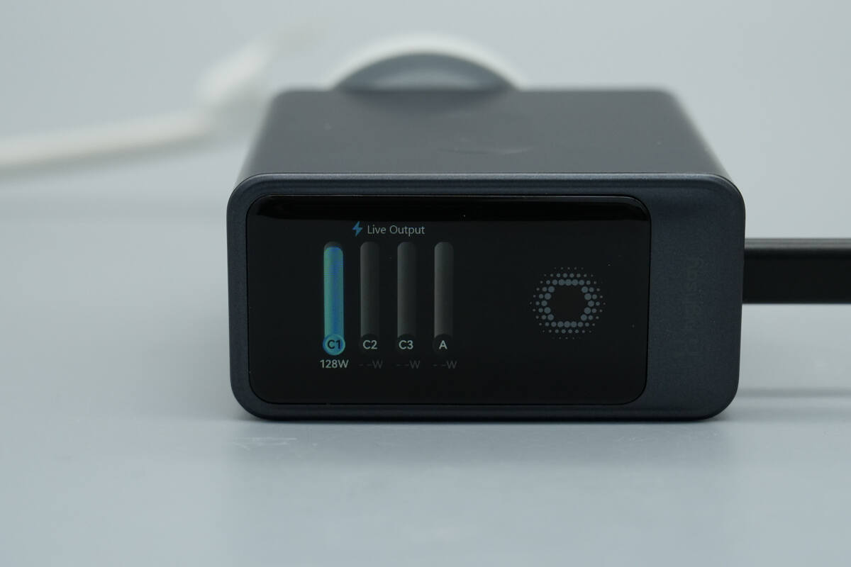
The multi-port power interface can display the real-time output power of each port.
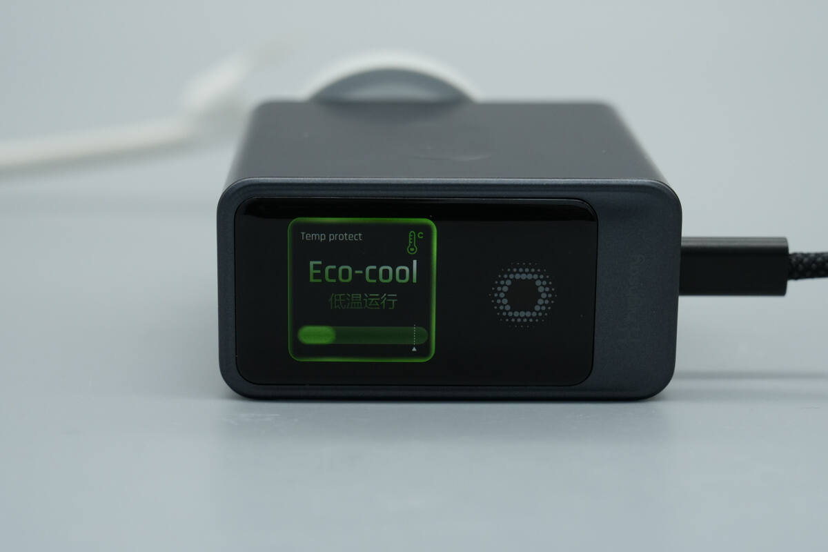
It can provide real-time feedback on the charger’s temperature rise through the temperature interface, offering a visual safety feature for more secure use.
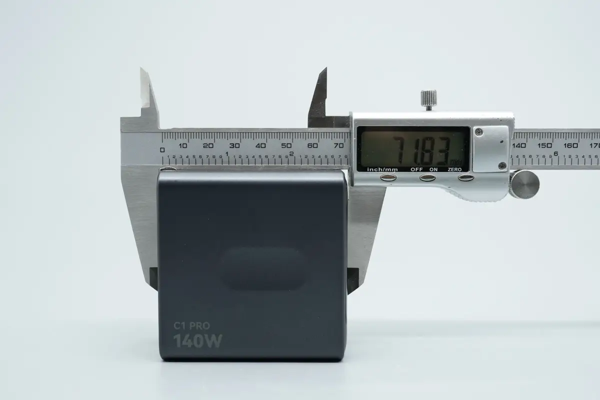
The length of the charger is about 71.83 mm (2.83 inches).
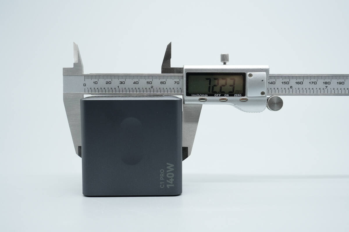
The width is about 72.23 mm (2.84 inches).
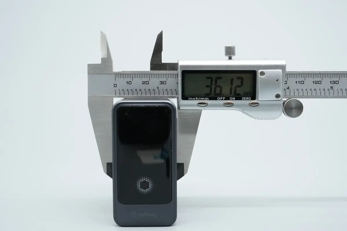
The thickness is about 36.12 mm (1.42 inches).
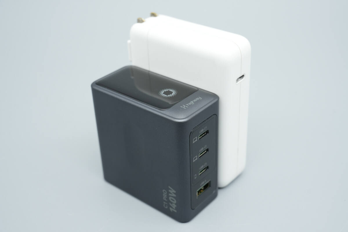
It is slightly smaller in size compared to the Apple 140W charger.
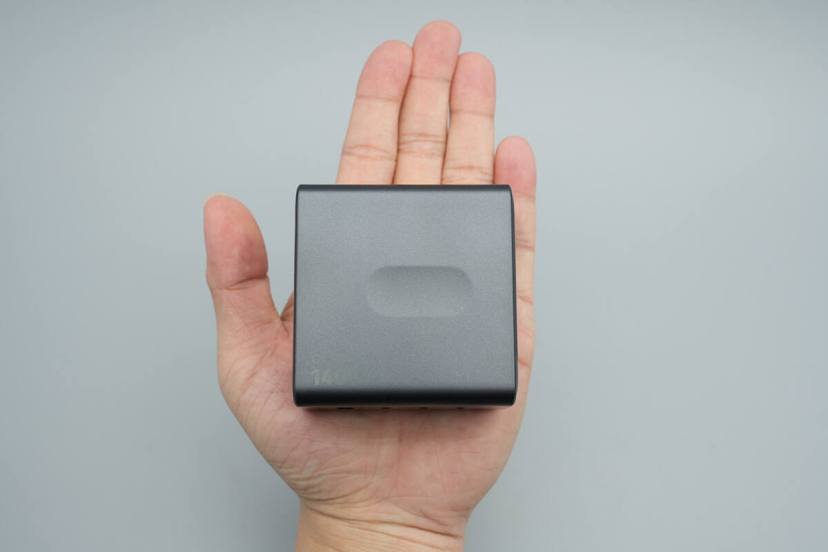
That's how big it is on the hand.
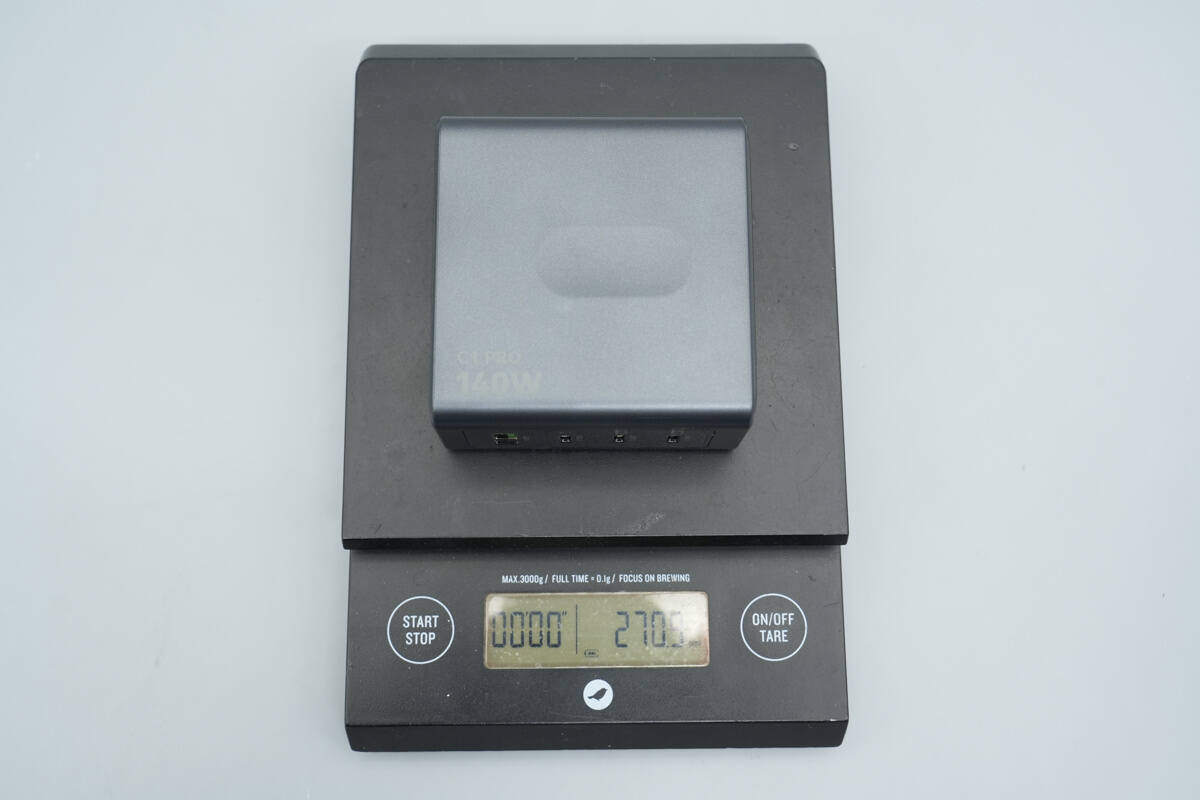
The weight is about 271 g (9.56 oz).
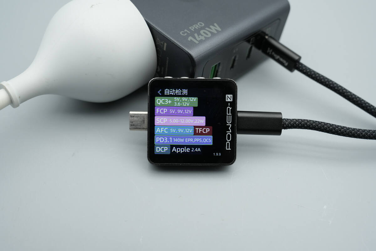
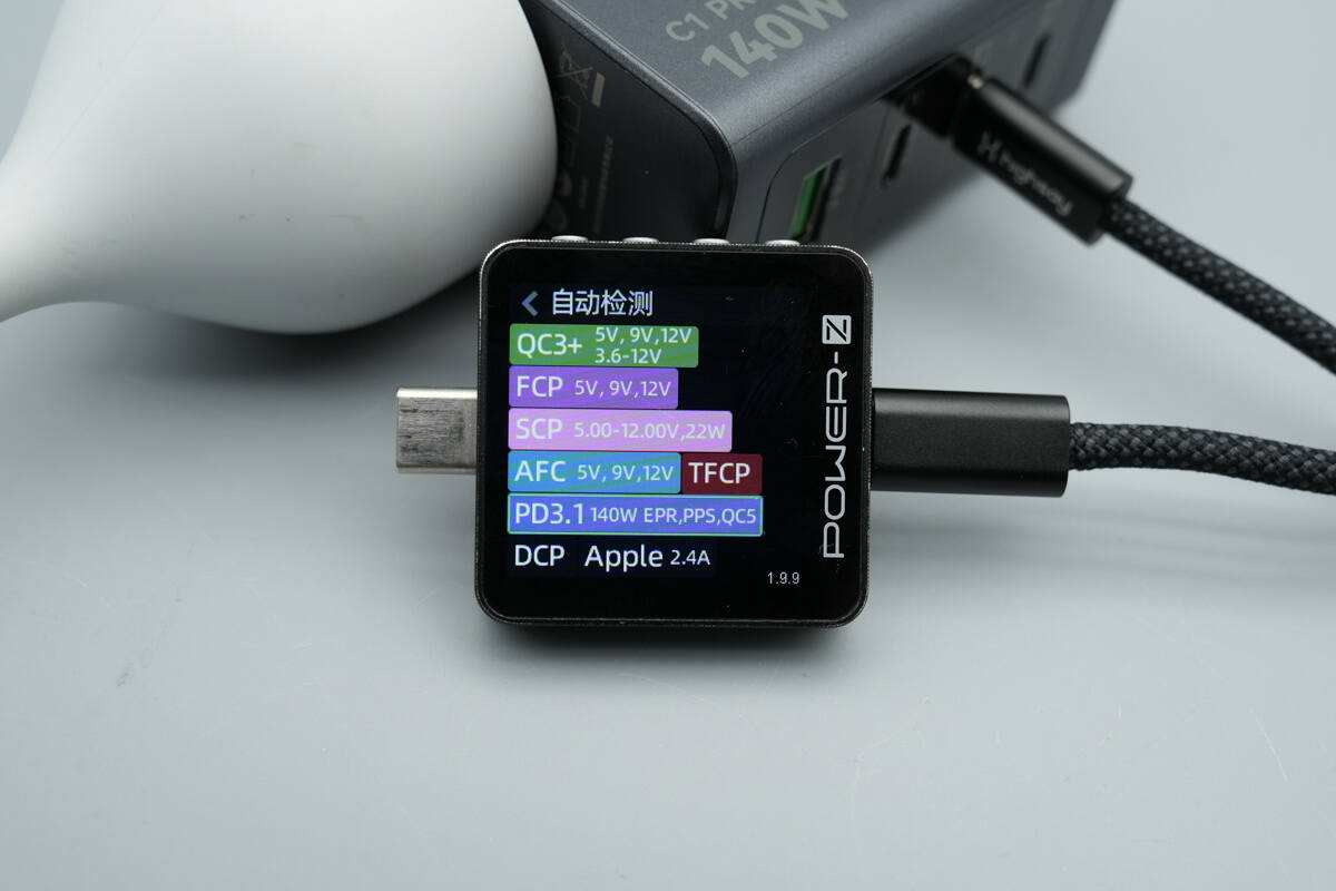
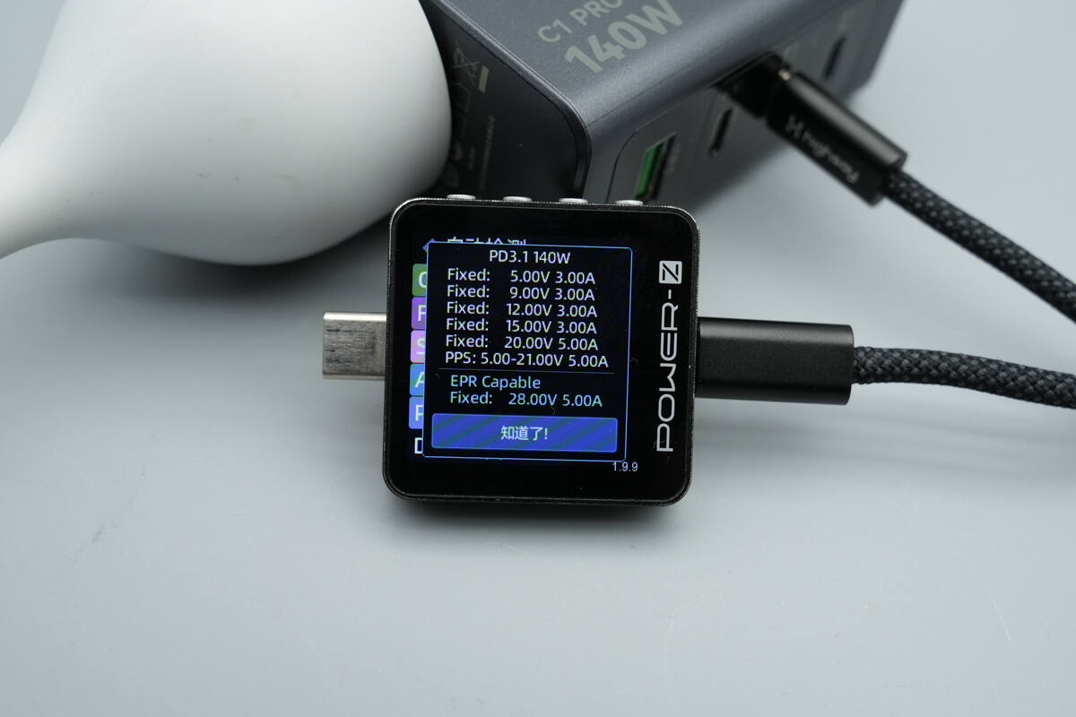
ChargerLAB POWER-Z KM003C shows that the USB-C1 supports QC3+/5, FCP, SCP, AFC, TFCP, PD3.1, PPS, DCP, and Apple 2.4A protocols.
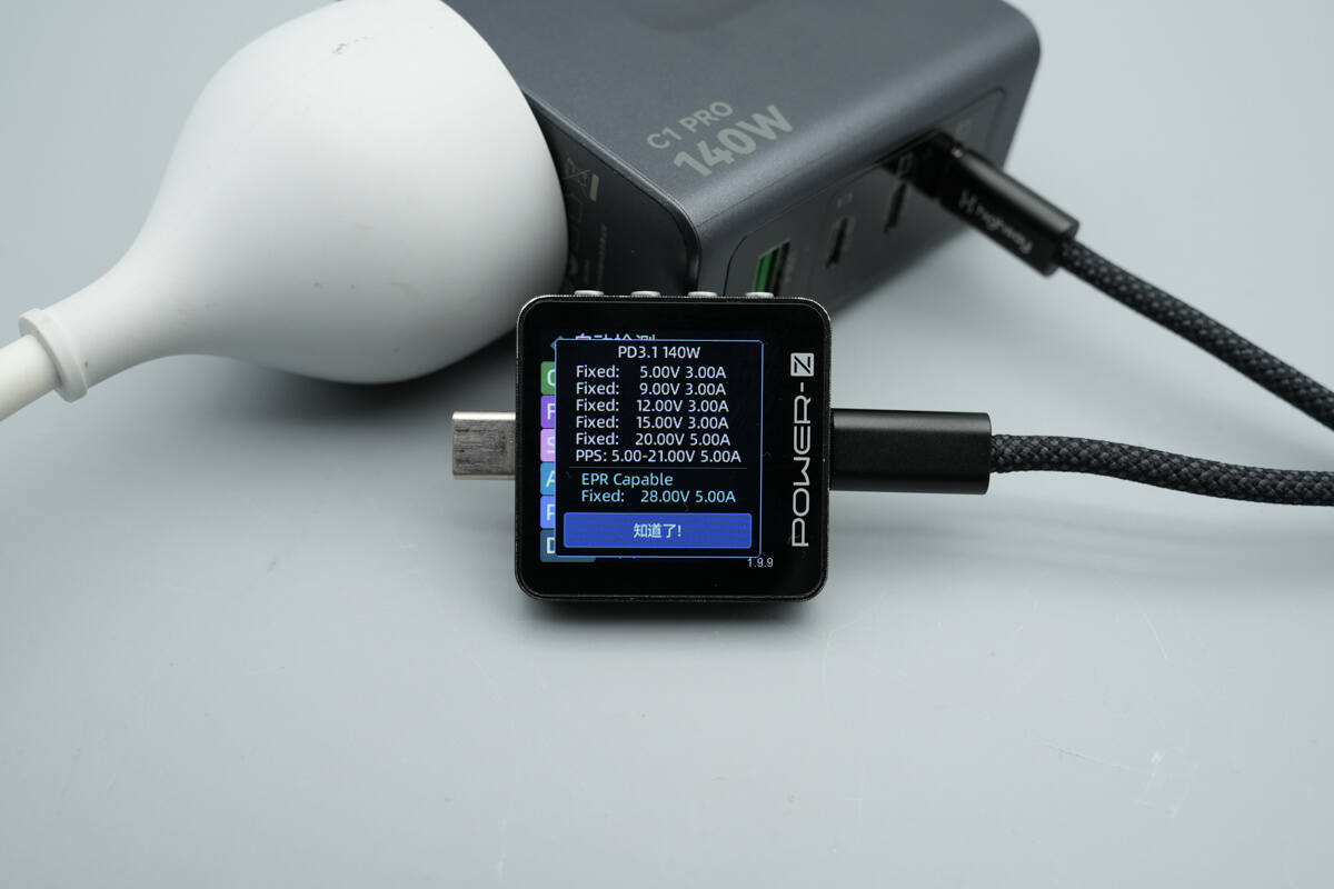
It has six fixed PDOs of 5V3A, 9V3A, 12V3A, 15V3A, 20V5A, and 28V5A, along with one set of PPS, which is 5-21V5A.
The USB-C2 port supports the same protocols as the USB-C1 port.
The PDO profiles are also identical.
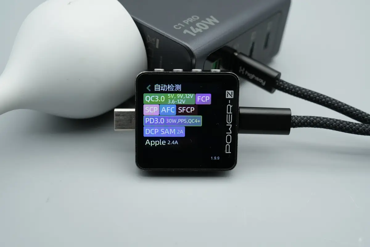
The USB-C3 supports QC3.0/4+, FCP, SCP, AFC, SFCP, PD3.0, PPS, DCP, SAM 2A, and Apple 2.4A protocols.

It has five fixed PDOs of 5V3A, 9V3A, 12V2.5A, 15V2A, and 20V1.5A, along with one set of PPS, which is 5-11V2.75A.

The USB-A supports QC3.0, FCP, SCP, AFC, SFCP, DCP, SAM 2A, and Apple 2.4A protocols.
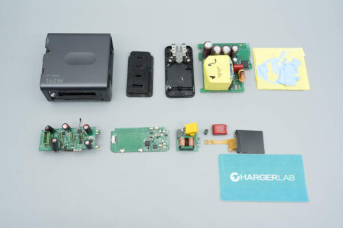
Teardown
Next, let's take it apart to see its internal components and structure.
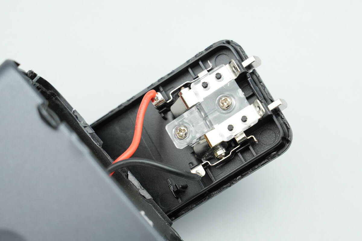
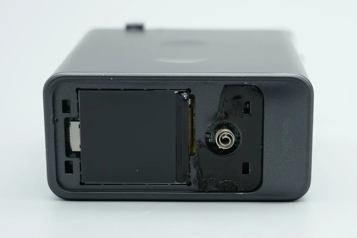
Open the input-side housing. The prongs are secured with a plastic plate and screws, and connected to the PCBA module via wires.

White adhesive is applied between the housing and the PCBA module to enhance the stability.
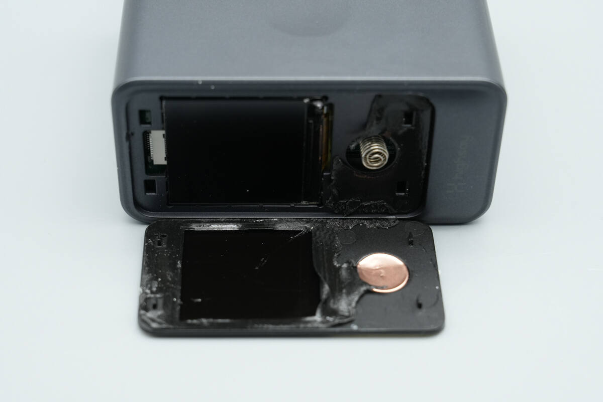
Remove the top cover; it is secured with double-sided adhesive.
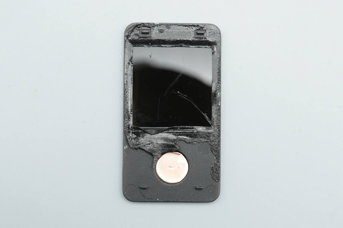
The cover has a window for the display, and copper foil is applied beneath the touch button area.
The display is connected to the PCBA module via a ribbon cable.
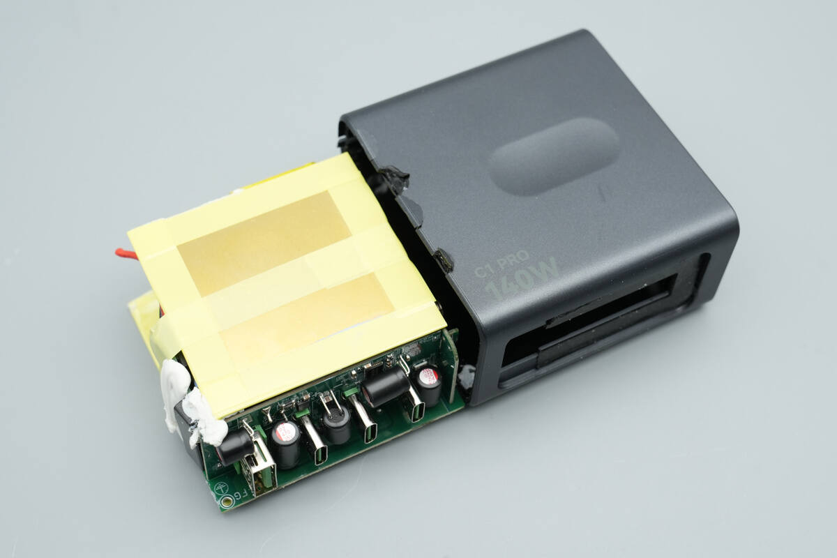
Detach the display and remove the PCBA module.
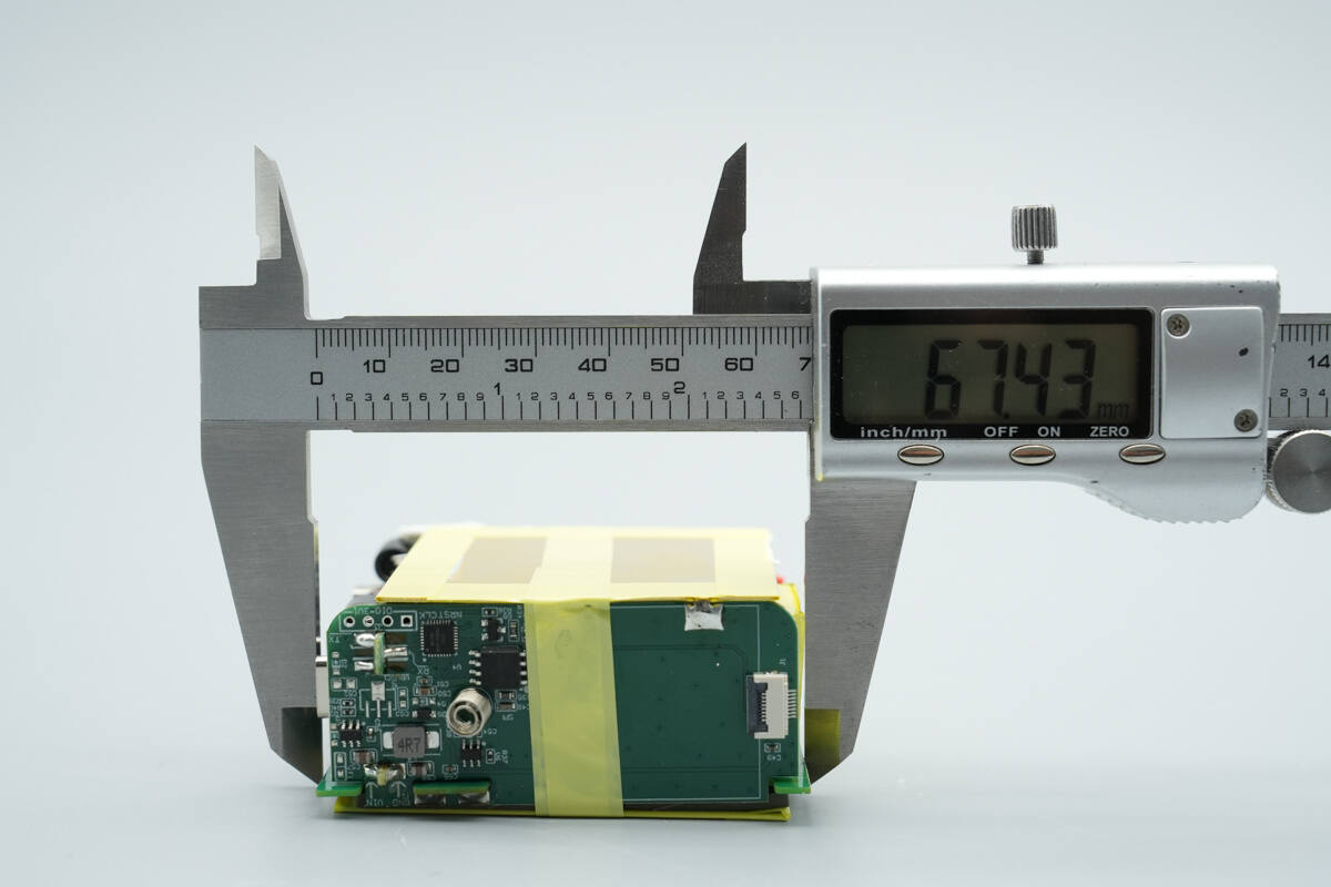
The length of the PCBA module is about 67.43 mm (2.65 inches).
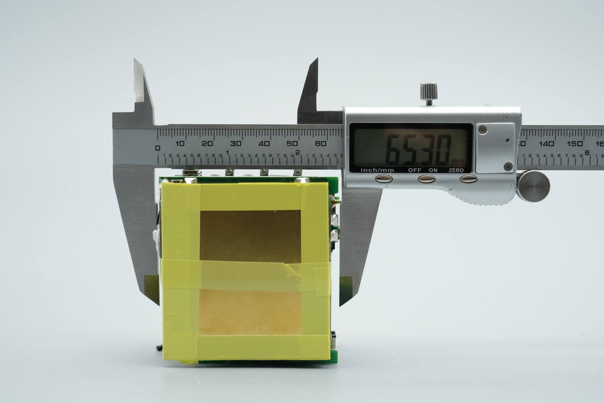
The width is about 65.3 mm (2.57 inches).
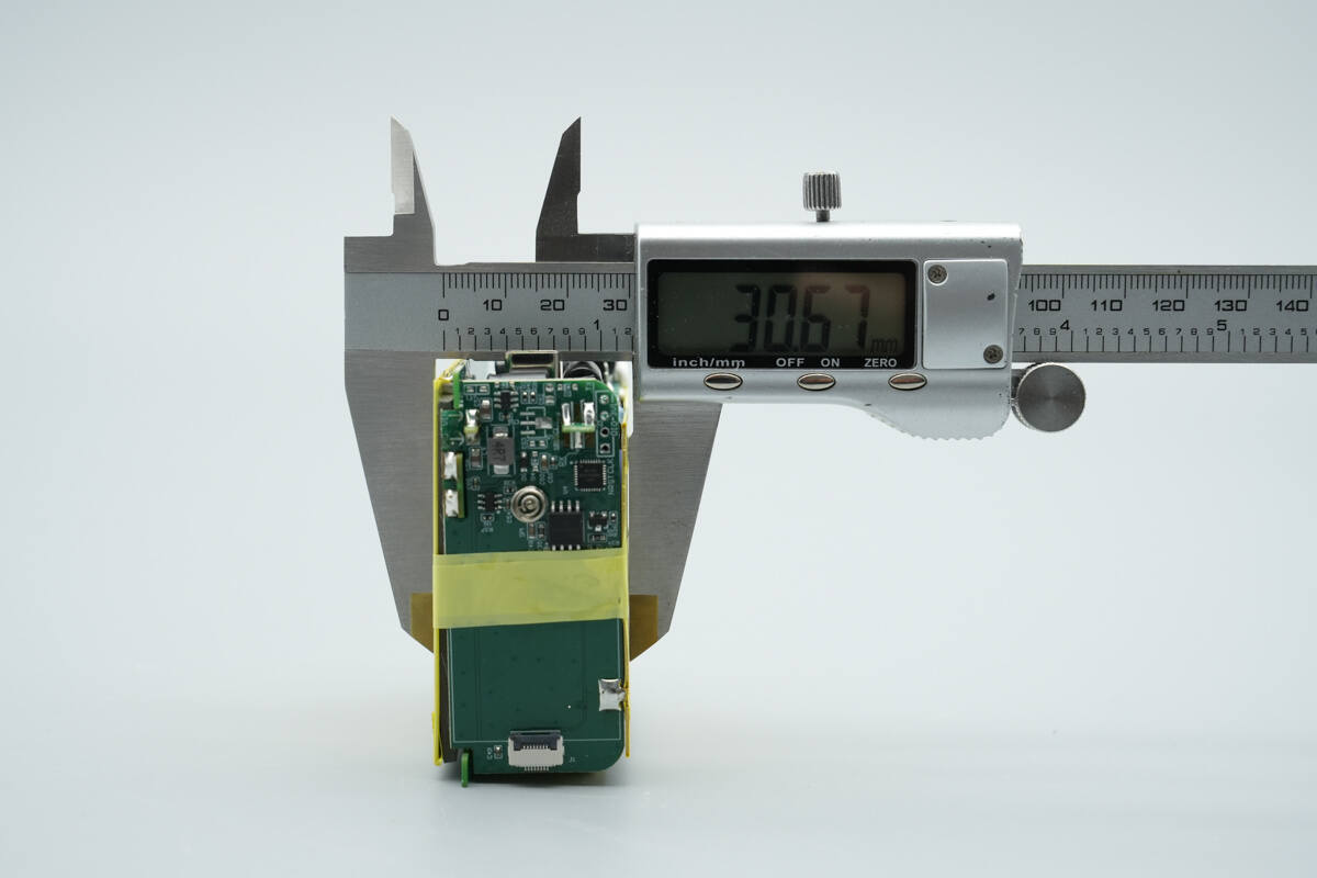
The thickness is about 30.67 mm (1.21 inches).

Both the top and bottom of the PCBA module are covered with brass heat sinks, which are additionally secured with tape.
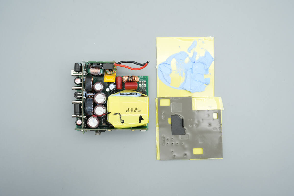
Remove the heat sinks; both metal plates have adhesive applied on the inner side and are equipped with thermal pads.

Small PCBs are soldered to both sides of the PCBA module as well as the output side. The central area contains high-voltage filter electrolytic capacitors, a capacitor that supplies power to the master control chip, and output filter capacitors, among other components.

On the back, there are bridge rectifiers, the primary master control chip, primary MOSFETs, a synchronous rectifier controller, and synchronous rectifiers, among other components.
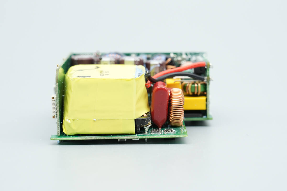
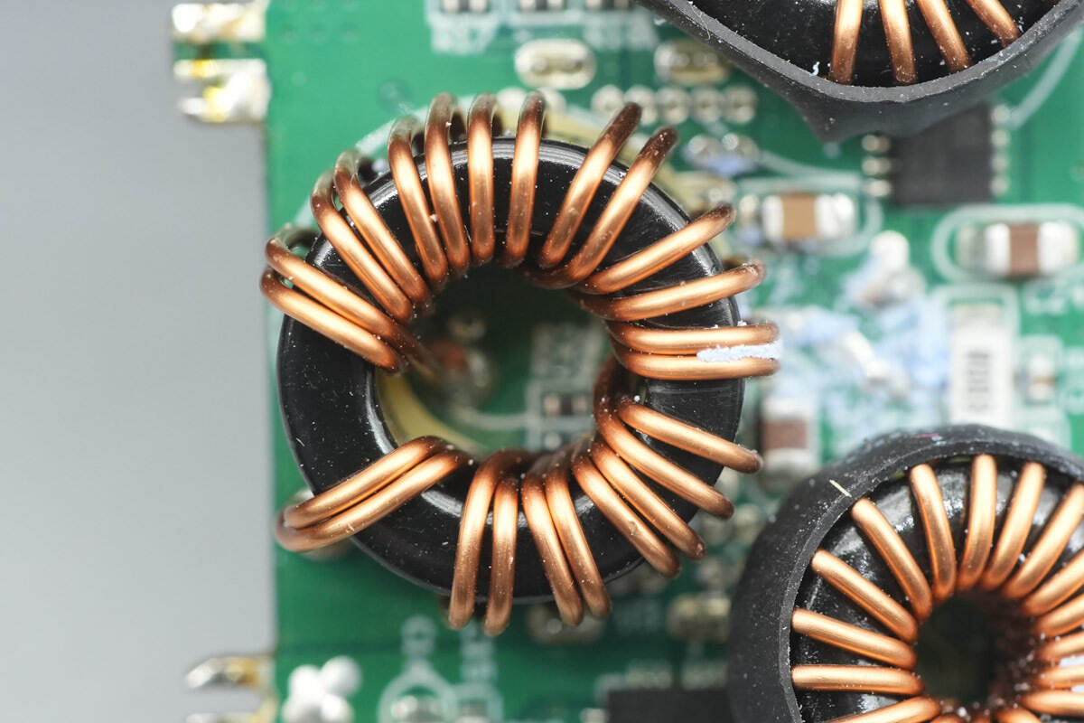
The front of the module contains a film capacitor, a filter inductor, a transformer, and other components.
On this side, there is a small input PCB soldered in place.
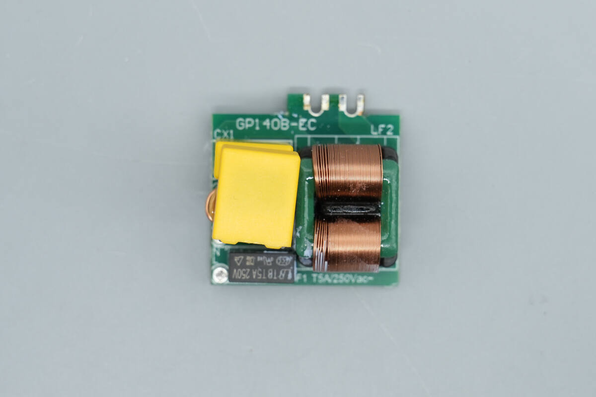
Remove the small PCB. The front side features a time-delay fuse, common mode chokes, and safety X2 capacitors.
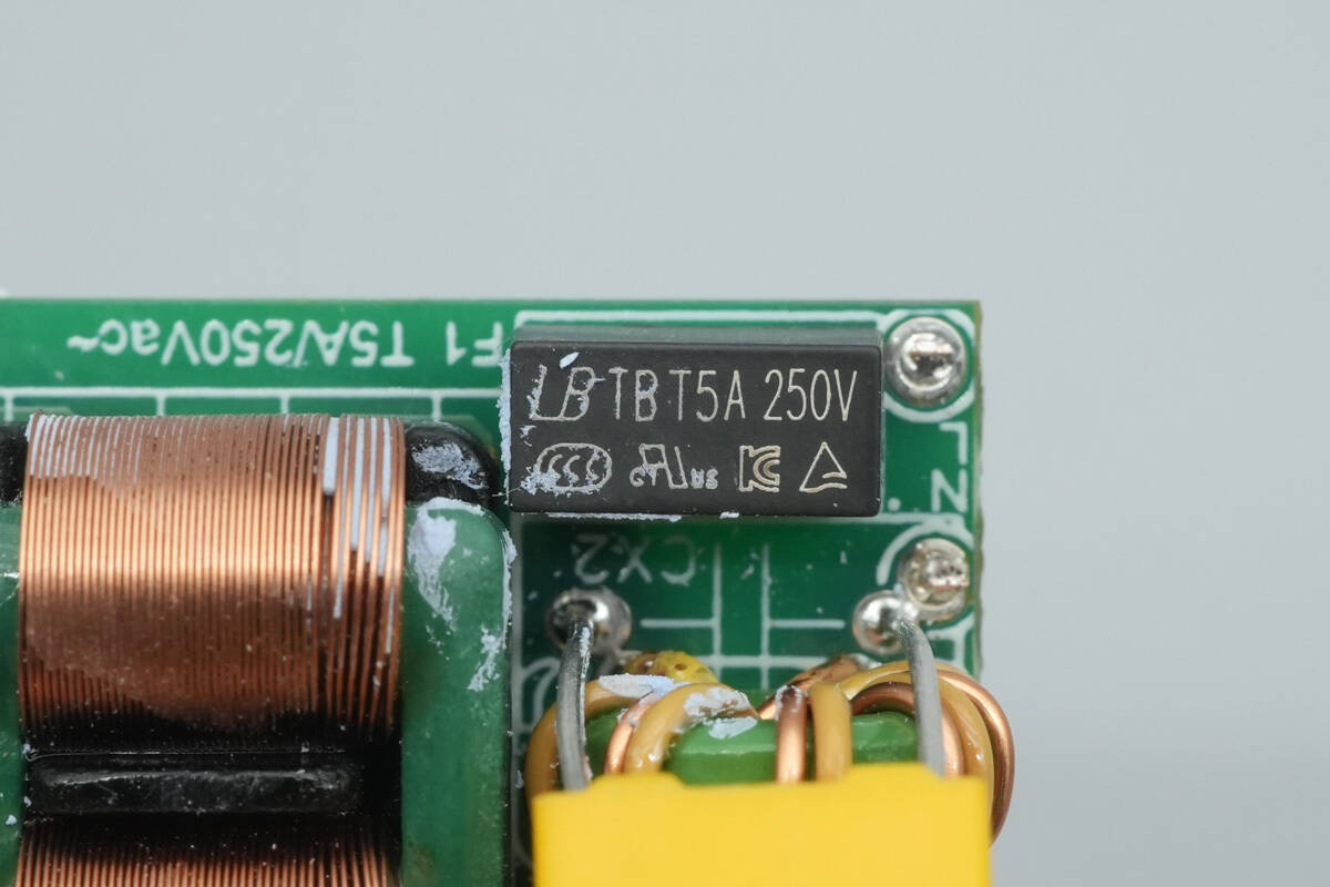
The time-delay fuse is from Lanbao, with a specification of 5A 250V.
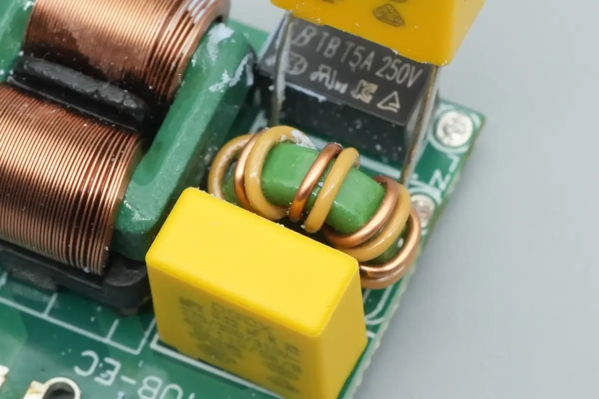
The common mode choke is wound with dual wires and is used to filter out EMI.

Close-up of the other common mode choke.
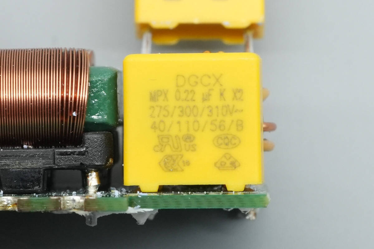
The safety X2 capacitor is from DGCX, with a capacitance of 0.22μF.
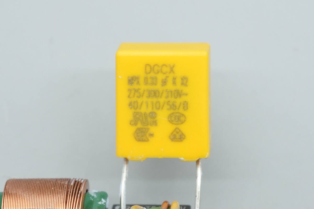
The other safety X2 capacitor is also from DGCX, with a capacitance of 0.33μF.

The bridge rectifier is from World Industrial, model WRLSB80M. This soft bridge rectifier features a softer recovery curve and smoother turn-off characteristics, which help reduce diode junction capacitance and minimize harmonic oscillation. The chosen LSB package offers excellent heat dissipation, enhancing the reliability of medium to high-wattage adapters. Each unit is capable of handling 60W or more.
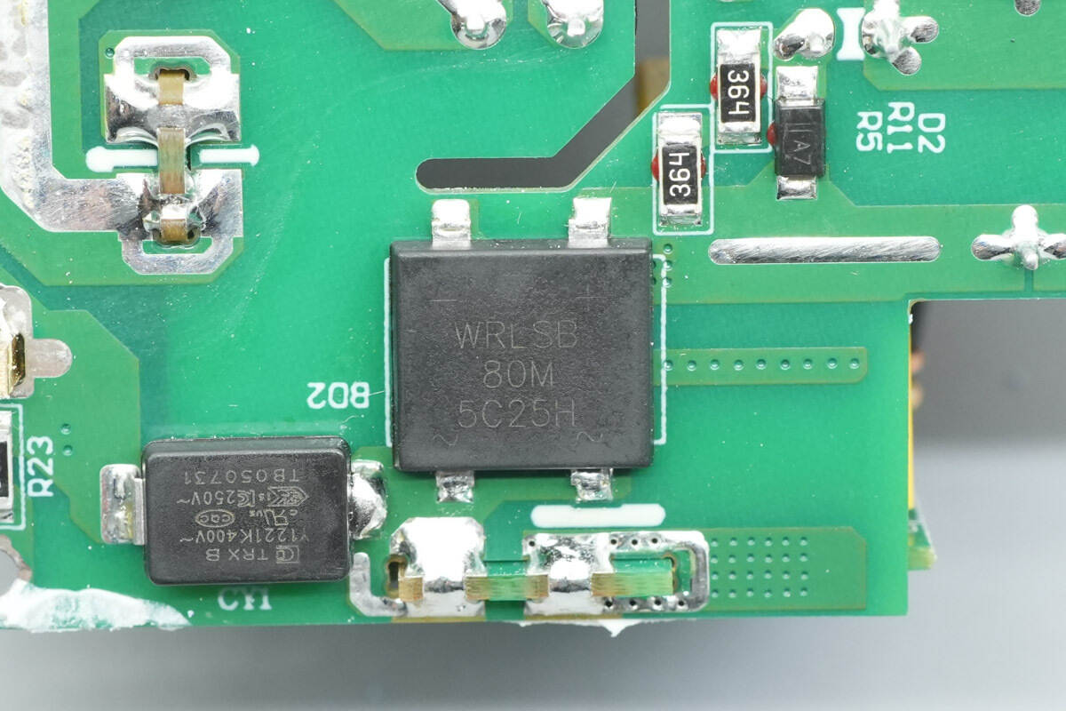
Close-up of the other World Industrial WRLSB80M bridge rectifier.
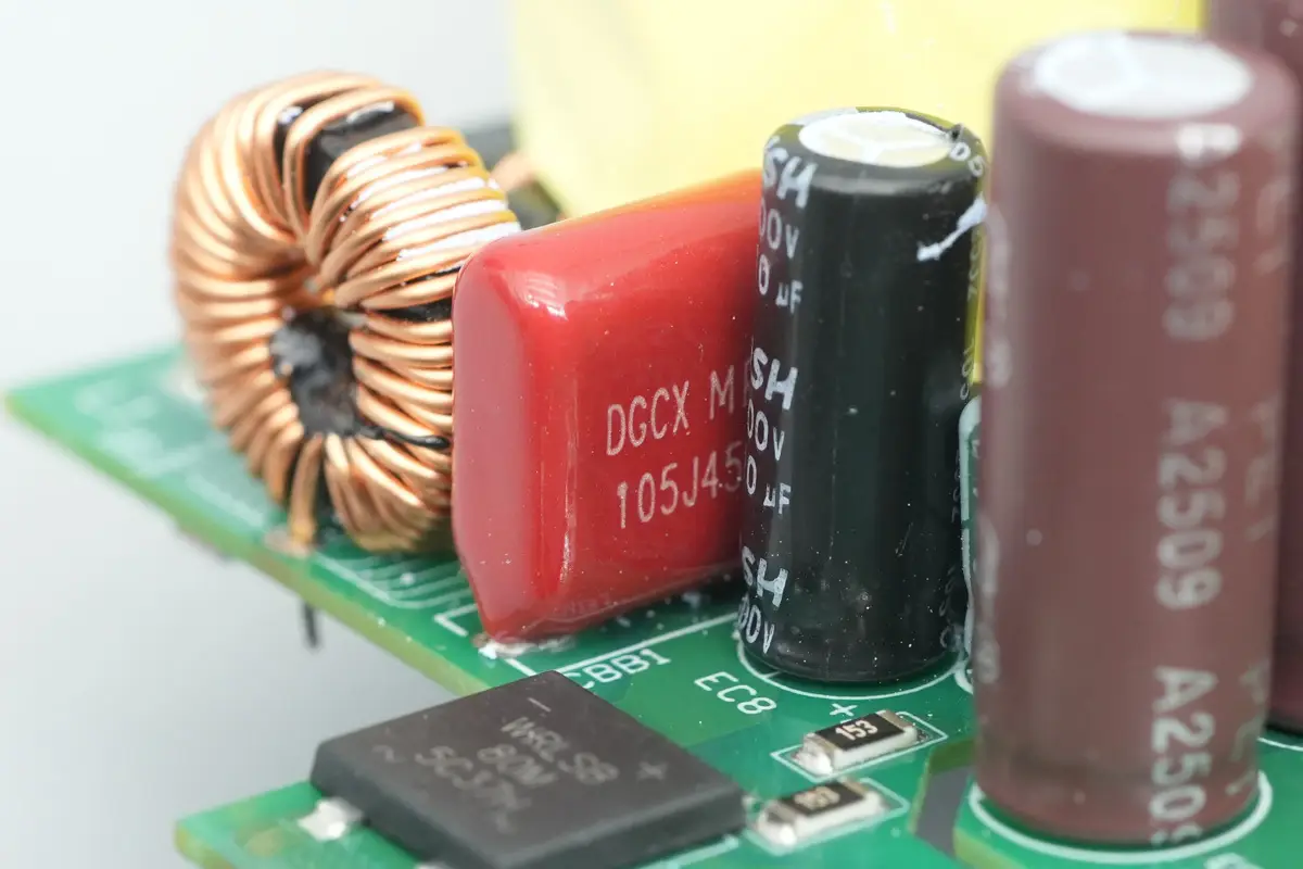
The film capacitor is from DGCX, with a specification of 1μF 450V.
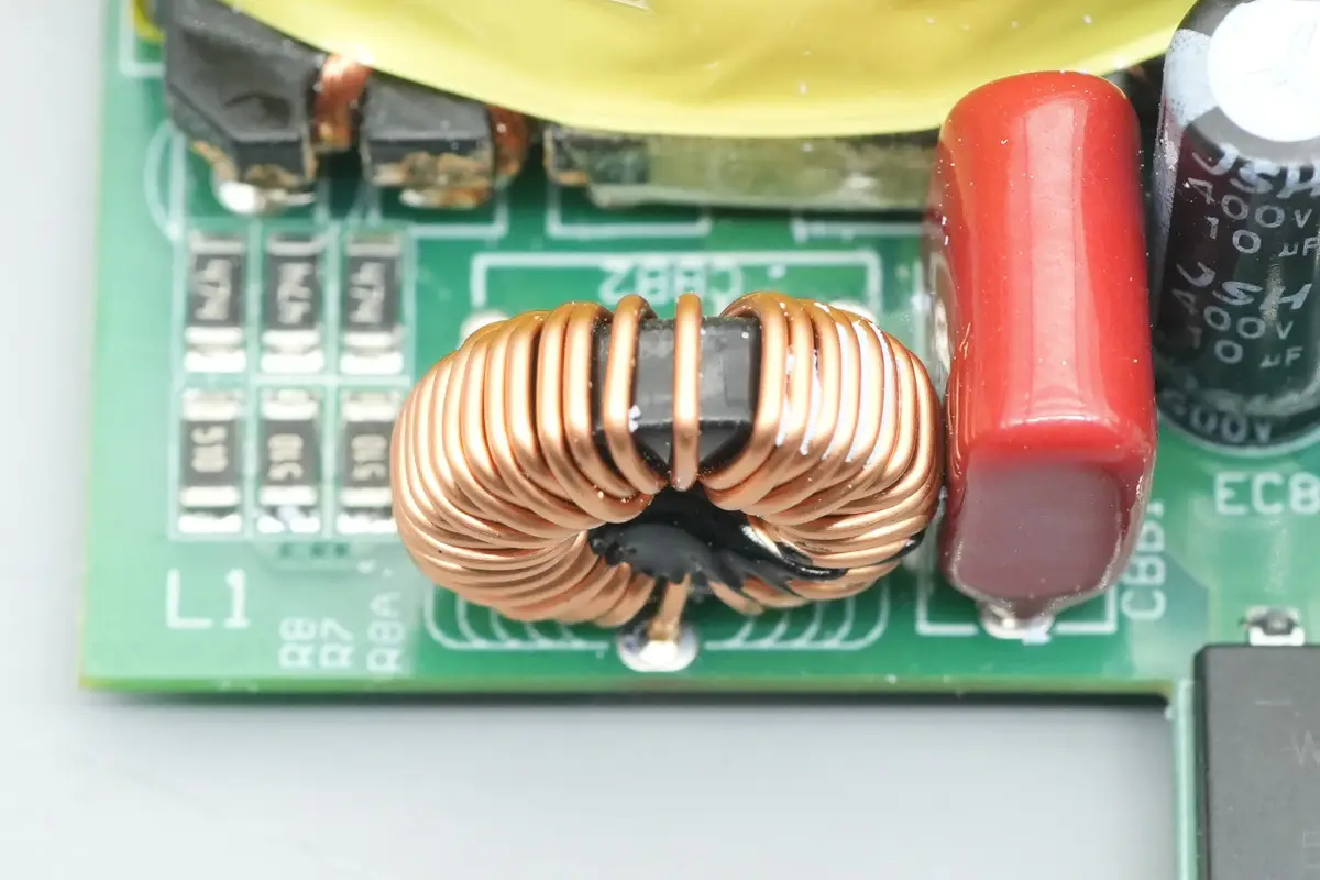
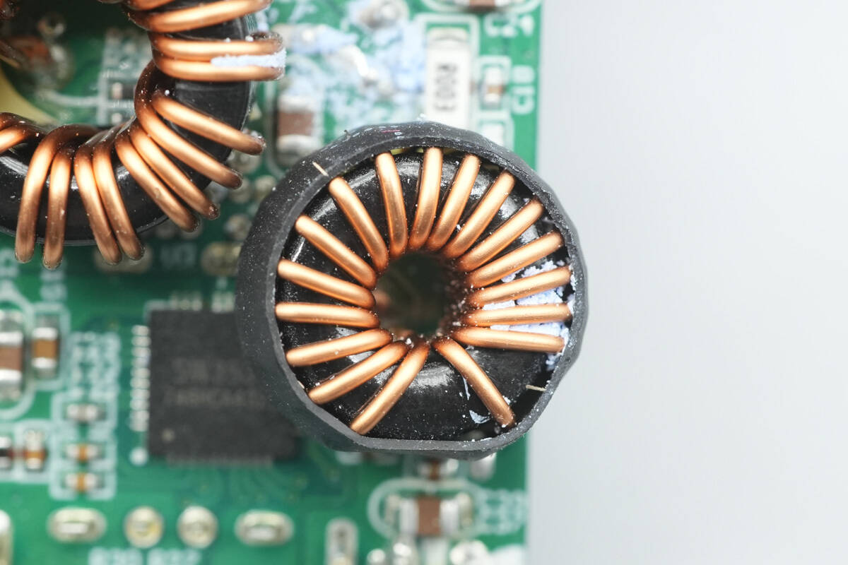
Close-up of the filter inductor.

The other film capacitor is also from DGCX, with a specification of 1.5μF 450V.
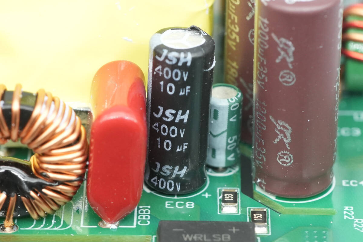
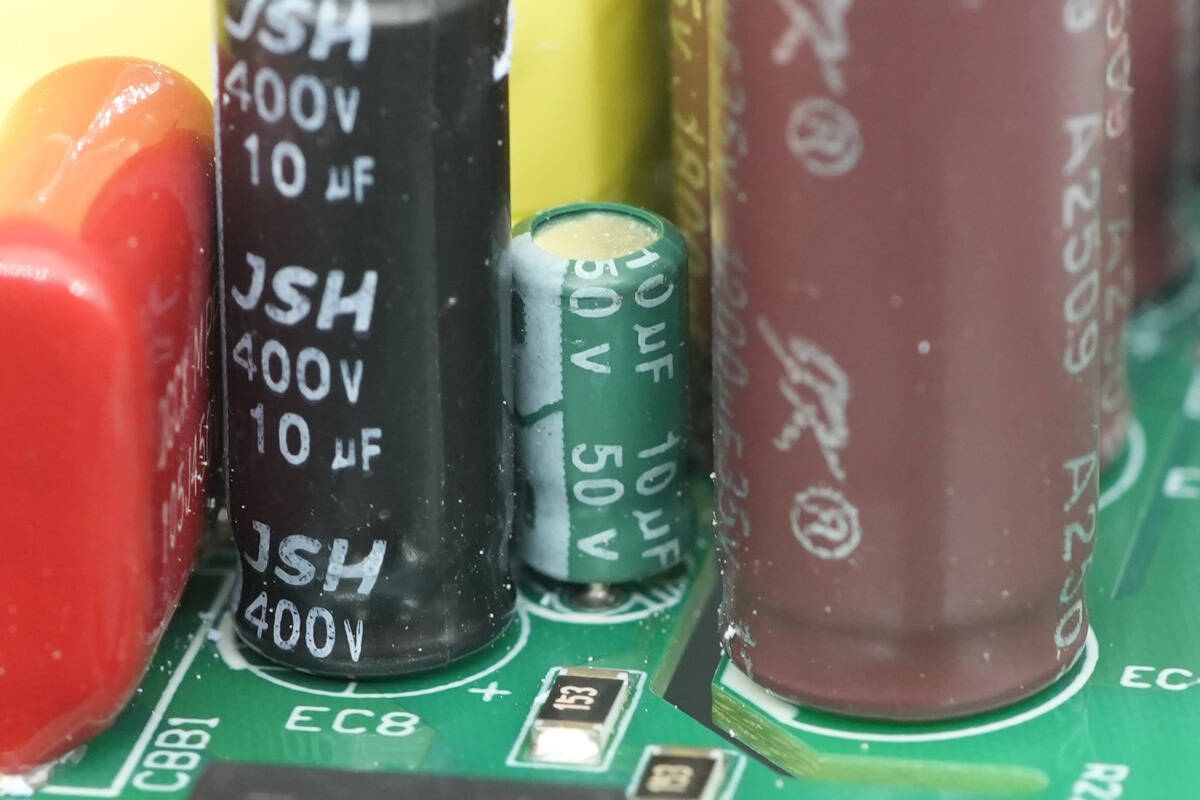
The high-voltage filter electrolytic capacitor is from JSH, with a specification of 400V 10μF.
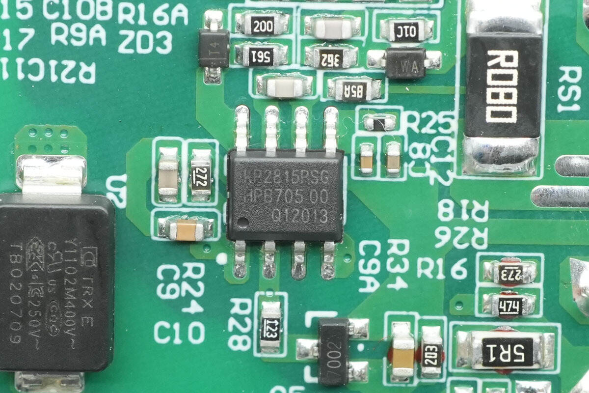
The primary master control chip is from Kiwi Instruments, model KP2815. This is a primary-side feedback high PF flyback constant voltage controller. The chip operates in a quasi-resonant, valley-switching mode, which results in high efficiency and good EMC performance. It integrates a high power factor algorithm and THD compensation, ensuring PF > 0.95 and THD < 10% across the full voltage range, and meets the requirements for light-load harmonic distortion.
The KP2815 uses primary-side feedback for constant voltage/constant current control. Under normal load conditions, it operates in constant voltage mode, with the chip sampling the output voltage through the auxiliary winding to maintain the output voltage at the reference value, achieving a constant voltage accuracy within ±3%. Under overload conditions, the chip switches to constant current control, sampling the primary-side resistance voltage in real time, and using an internal high-precision constant current control algorithm to regulate the output current, with control accuracy within ±7%.
The KP2815 integrates an adaptive high-sensitivity fast dynamic response mechanism, which controls output voltage overshoot/undershoot within a small range when the output load changes dynamically. It also features adaptive input voltage detection, with a frequency dithering function when operating with DC input, helping to reduce noise at the switching frequency and minimizing the size of the input filter.
The chip is equipped with comprehensive protection features to ensure the safe and reliable operation of the system, including: input overvoltage/undervoltage protection, cycle-by-cycle current limiting (OCP), overtemperature protection (OTP), auto-oscillation protection during startup and short-circuit conditions (AOCP), output overvoltage protection (OVP), and output short-circuit protection (SCP), among others.
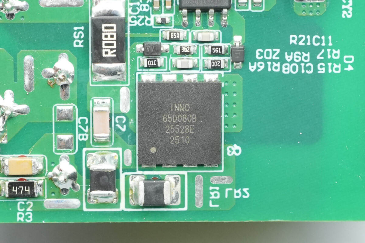
The primary MOSFET is from Innoscience, model INN650D080B. This is an enhanced GaN FET with a voltage rating of 650V and a transient voltage rating of 800V. It has a drain-source resistance (Rds(on)) of 80mΩ. The MOSFET supports ultra-high switching frequencies, features no reverse recovery charge, and has very low gate charge and output charge. It meets industrial application requirements per JEDEC standards, includes built-in ESD protection, and complies with RoHS, lead-free, and EU REACH regulations.

Here is the information about Innoscience INN650D080B.
The capacitor that powers the master control chip has a specification of 50V 10μF.
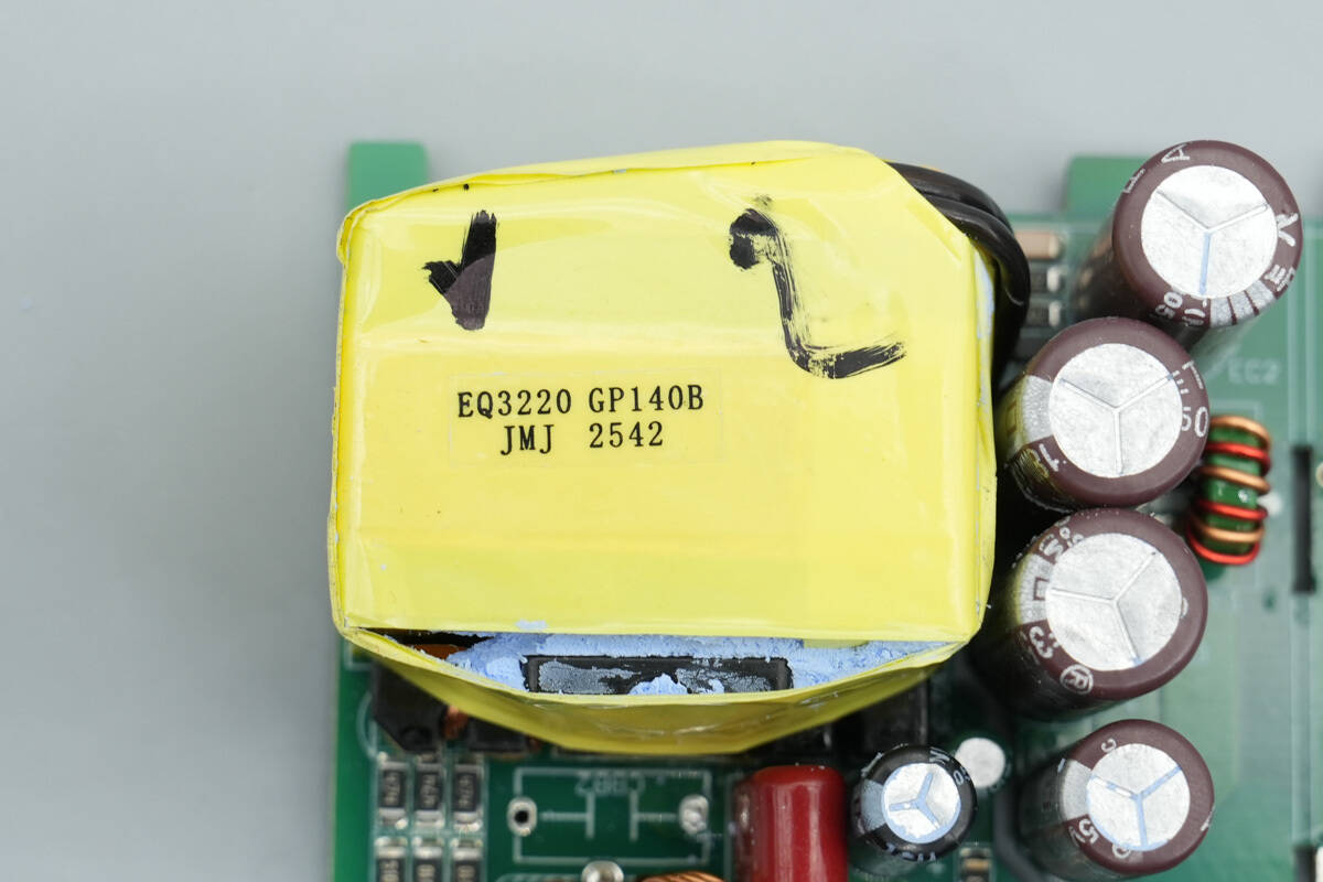
Close-up of the transformer.

The OR 1008 optocoupler is used for output voltage feedback.

The SMD Y capacitor is from TRX. Its compact size and light weight make it ideal for high-density power products like GaN fast chargers. The part number is TMY1221K.
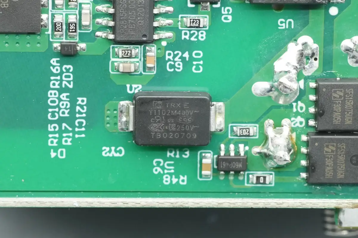
The other TRX SMD Y capacitor has the part number TMY1102M.
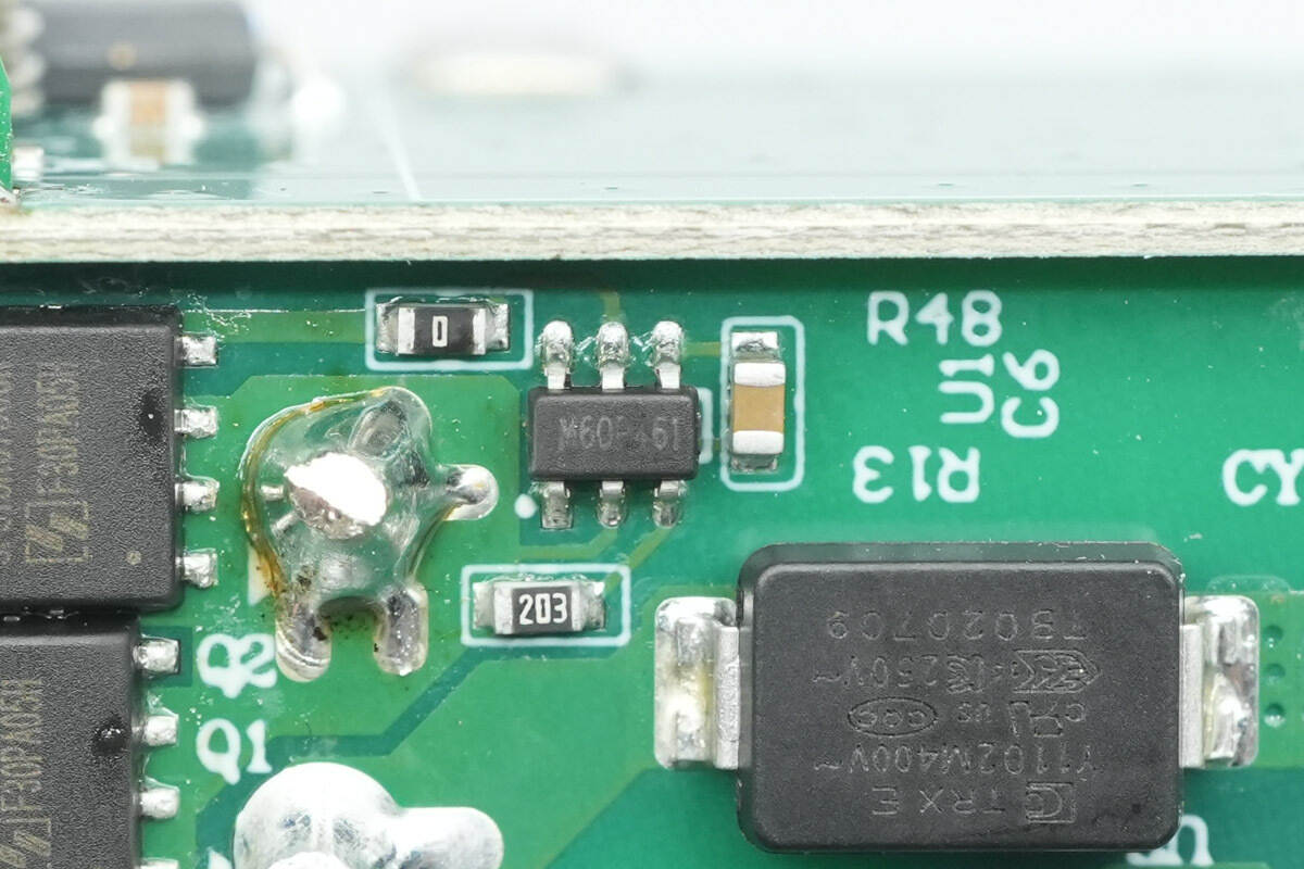
The synchronous rectifier controller is from Kiwi Instruments, model KP4060, marked with M60. It supports DCM, CCM, and QR operating modes, as well as active clamped Flyback topology. The chip supports a 600kHz operating frequency and integrates high-voltage detection circuits and high-voltage power supply circuits. It also includes intelligent dual LDOs, eliminating the need for auxiliary winding power supply, and supports output short-circuit SR operation. The controller is packaged in a space-saving SOT23-6 form factor.
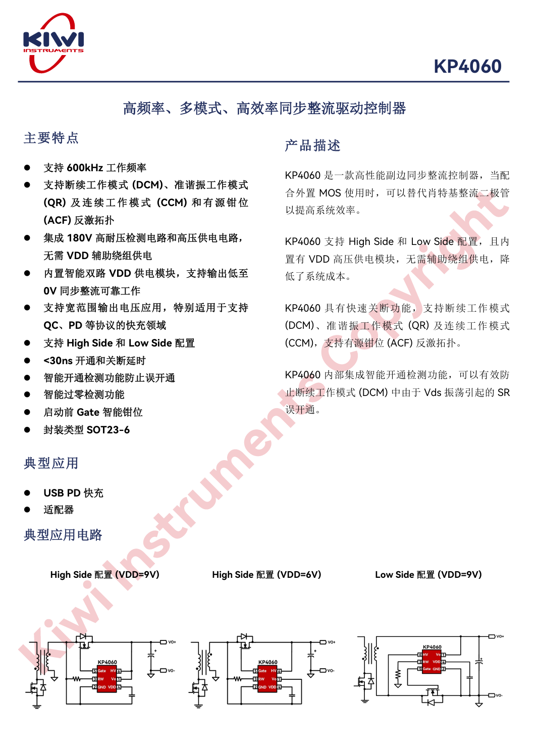
The KP4060 supports a wide range of output voltage applications, making it particularly suitable for fast charging fields that support protocols like QC and PD. It also supports both high-side and low-side configurations. The chip features a <30ns turn-on and turn-off delay, along with gate drive clamping technology to prevent false turn-on caused by parasitic coupling. It incorporates patented intelligent zero-crossing current detection and smart turn-on detection technologies to avoid false triggering, ensuring safe operation.
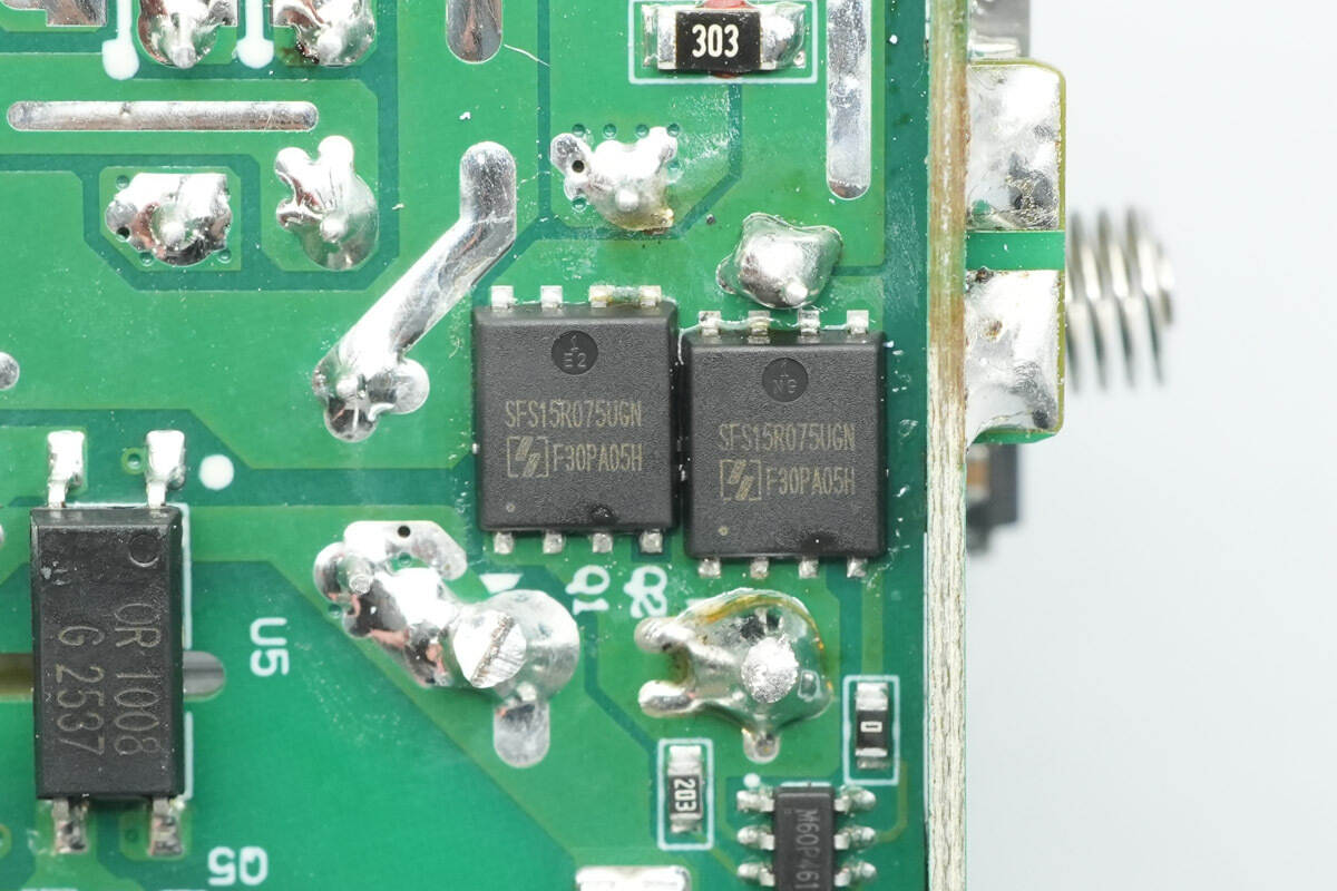
The synchronous rectifiers are from Oriental, model SFS15R075UGNF. These are NMOS transistors with a voltage rating of 150V and a drain-source resistance (Rds(on)) of 8mΩ. They come in a PDFN 5x6 package.

All four output filter capacitors are from JK. This one has a specification of 35V 1200μF.

These two capacitors have a specification of 35V 1800μF.
The fourth capacitor has a specification of 35V 1800μF.
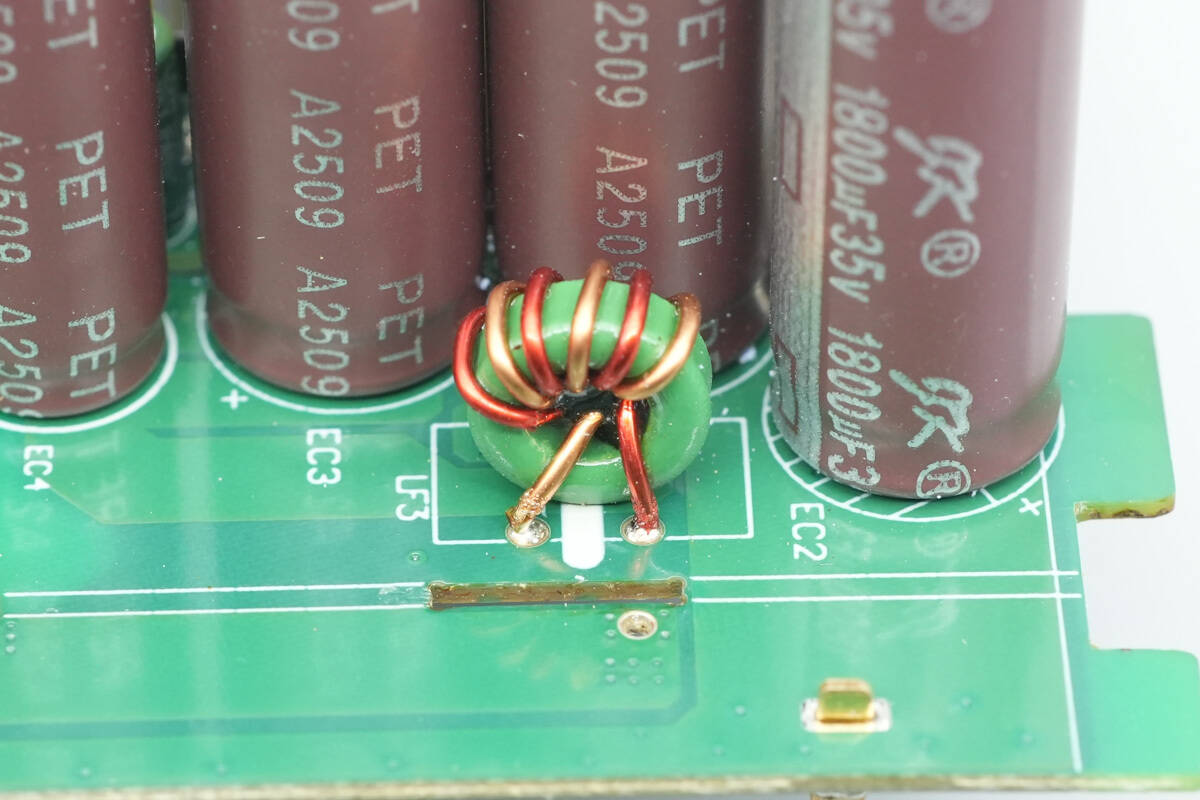
Close-up of the filter inductor.
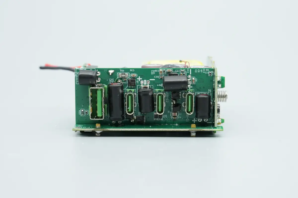
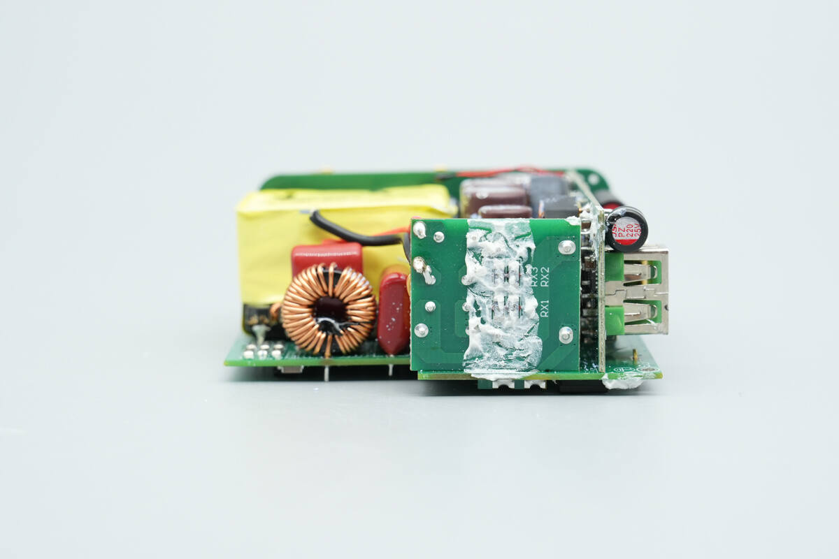
The output side is soldered with a USB interface PCB.
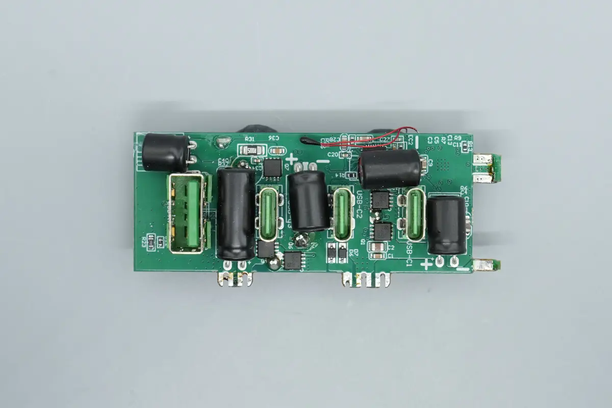
Remove the PCB. The front side features a buck protocol chip, synchronous buck MOSFETs, VBUS MOSFETs, and solid capacitors.
The back features buck protocol chips, buck inductors, VBUS MOSFETs, and other components.
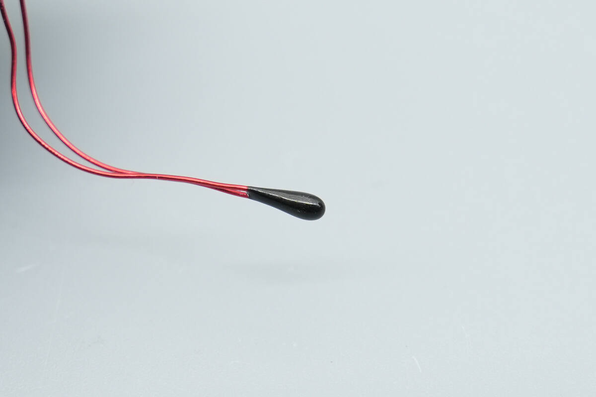
Close-up of the thermistor.
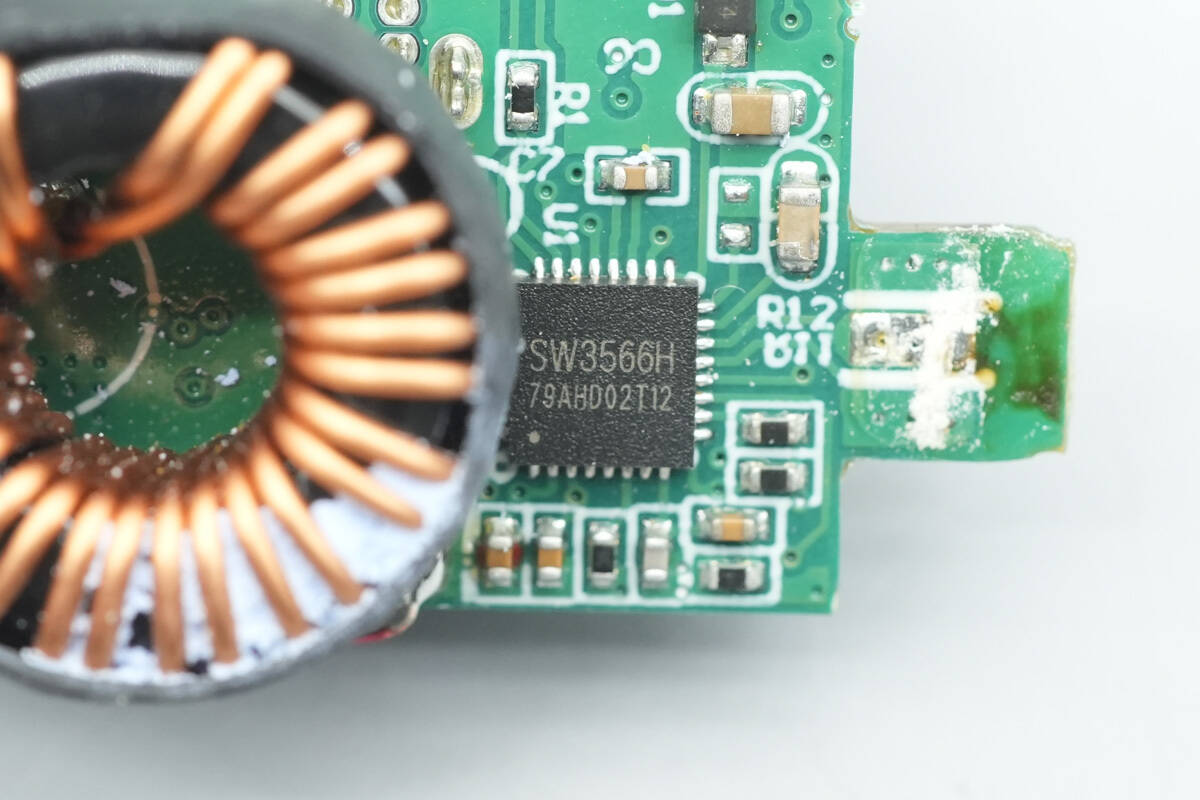
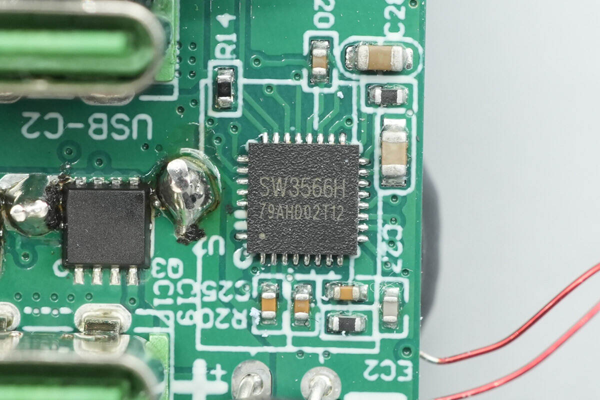
The buck protocol chip for USB-C1 is from iSmartWare, model SW3566H. It is a highly integrated multi-fast-charging protocol dual-port charging SoC that supports USB-C and USB-A charging, with independent current limiting for each port. The chip integrates a high-efficiency synchronous buck converter, supporting outputs of 20V 7A and 28V 5A, and is compatible with fast charging protocols like PD3.1, QC, SCP, UFCS, and custom fast charge protocols. It can support a maximum output power of 140W.
The SW3566H chip integrates CC/CV modes, dual-port management logic, and bus voltage detection. When paired with the corresponding buck MOSFETs and VBUS MOSFETs, it achieves dual-port buck output. The built-in buck converter operates at a frequency of 180kHz, supporting both PWM and PFM operating modes. Protection thresholds for output current, line loss compensation, and more can be set via the I2C interface. The integrated ADC allows for data sampling of 9 channels, including input/output voltage, output current, and chip temperature, and supports an external MCU for parameter display.
It supports a 36V input voltage and a maximum output current of 7A. The chip also features soft start, input overvoltage/undervoltage protection, output overvoltage/undervoltage protection, output overcurrent/short-circuit protection, DP/DM/CC overvoltage protection, chip overheat protection, external NTC thermistor protection, and power limit protection. It comes in a QFN 4x4-32 package.
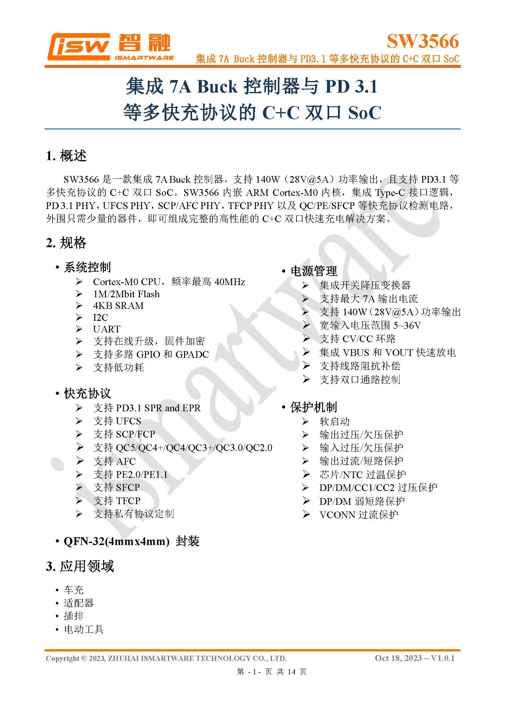
Here is the information about iSmartWare SW3566.
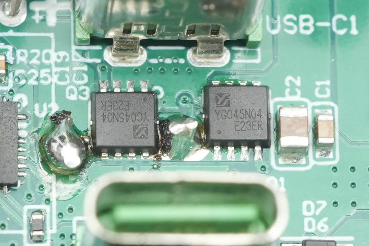
The paired synchronous buck MOSFETs are from YouCrystal, model YG045N04ADE, with a voltage rating of 40 V and an on-resistance of 4.5 mΩ, housed in a PDFN 3×3 package.

The paired buck inductor is insulated with a heat-shrink sleeve.
The buck protocol chip for the USB-C2 port also uses the iSmartWare SW3566H.

The paired synchronous buck MOSFETs are also YouCrystal YG045N04ADE.
Close-up of the paired buck inductor.
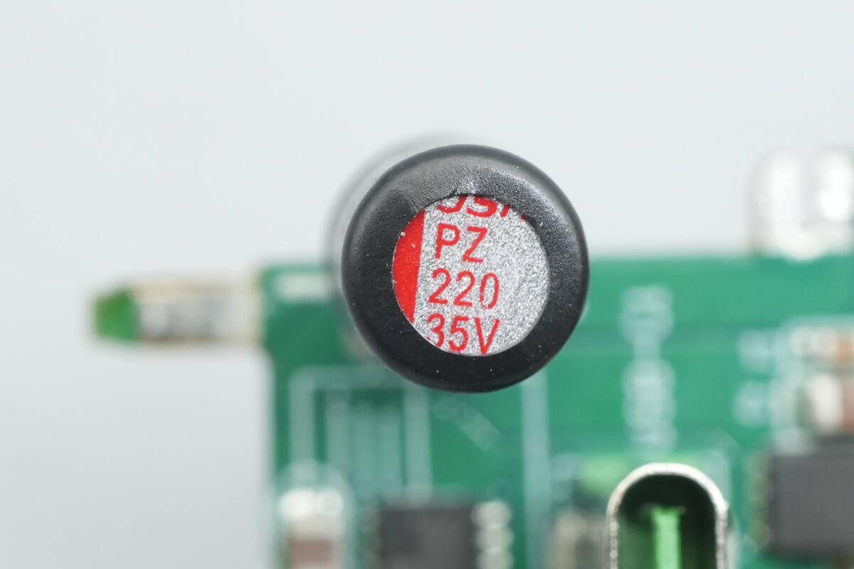
The solid capacitor is from JSH, with a rating of 35 V and 220 μF.
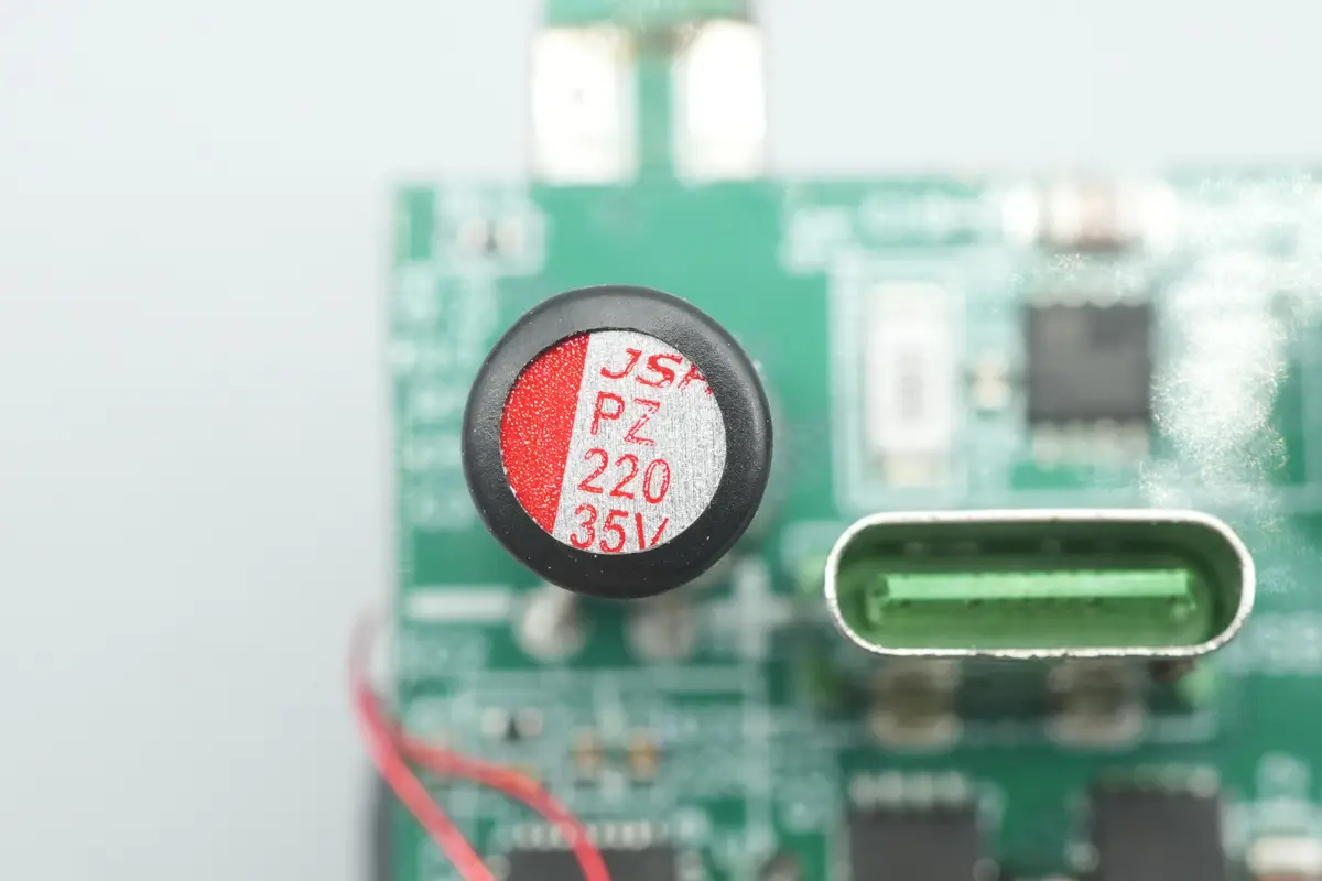
The other solid capacitor has the same specifications.
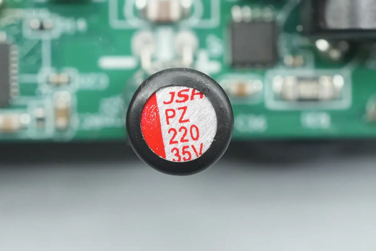
The third solid capacitor is also identical.
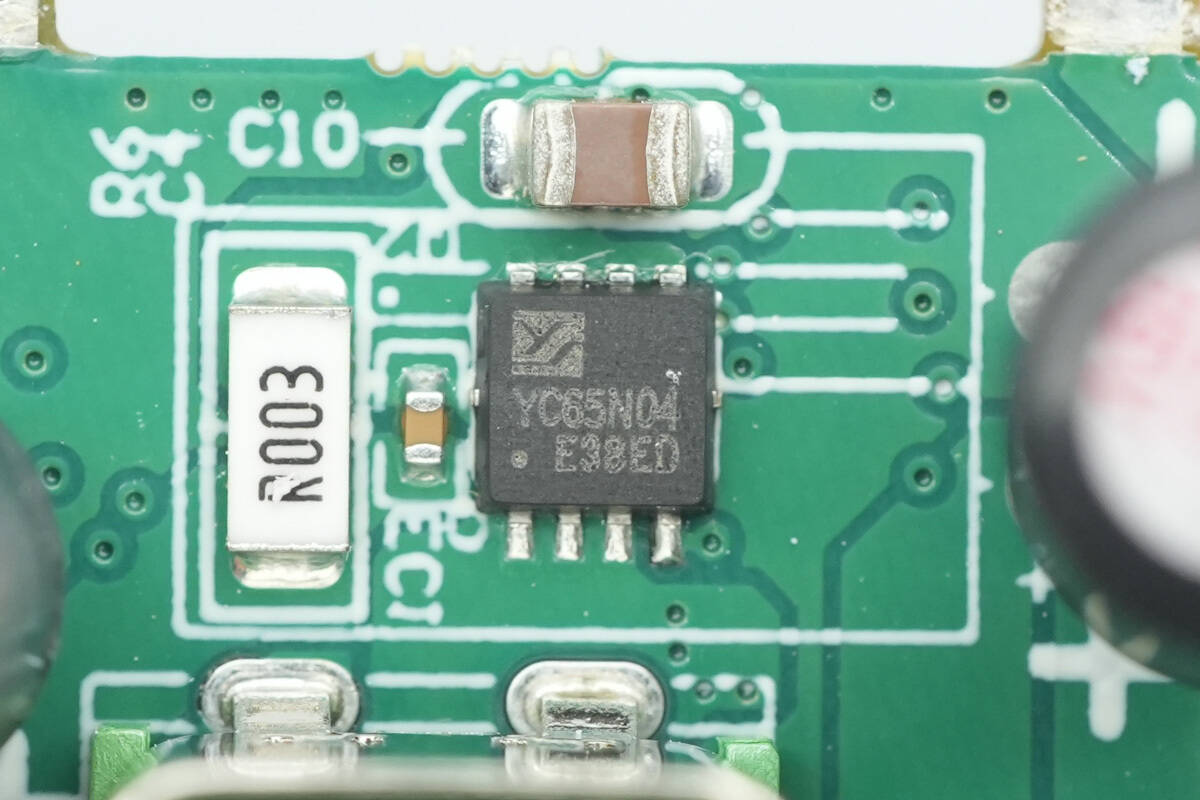
The output VBUS MOSFET for the USB-C1 port is from YouCrystal, model YC65N04ADE, NMOS, with a voltage rating of 40 V and an on-resistance of 4.8 mΩ, housed in a PDFN 3×3 package.

The VBUS MOSFET for the USB-C2 port is also YouCrystal YC65N04ADE.
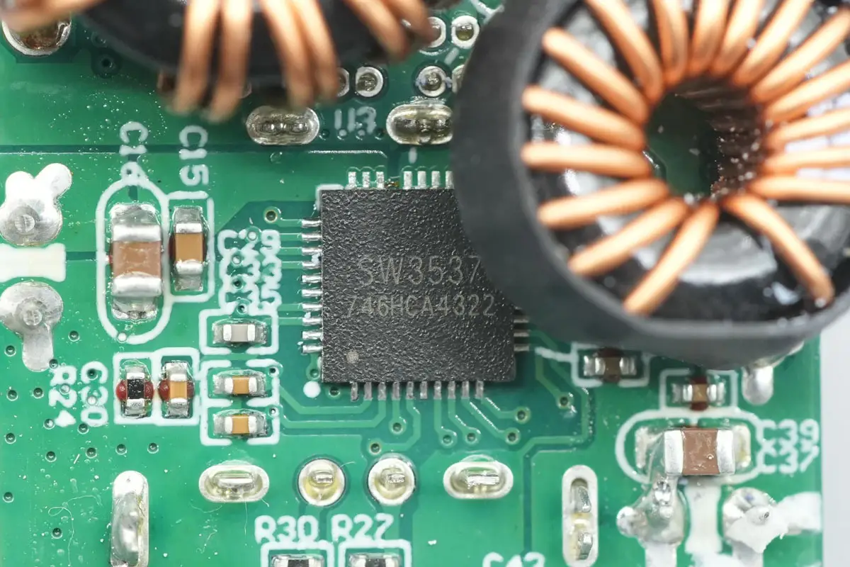
The buck protocol chip for the USB-C3 and USB-A ports is from iSmartWare, model SW3537. It integrates a 5 A high-efficiency synchronous buck converter and supports PPS, PD, QC, AFC, FCP, SCP, PE, SFCP, and low-voltage direct charging protocols. The chip operates in CC/CV mode and requires only a minimal number of external components to form a complete high-performance dual-port fast-charging solution.
Thanks to its high level of integration, the SW3537 combines the traditional buck system’s protocol chip, synchronous buck controller, and MOSFETs within a single package, greatly simplifying multi-port fast-charging circuit design. It supports dual-port A+C fast charging applications and includes comprehensive protection features.
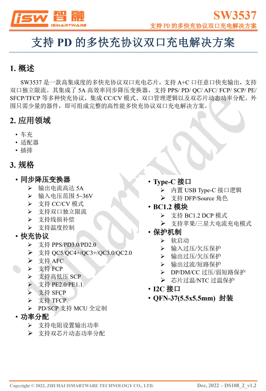
Here is the information about iSmartWare SW3537.
The paired buck inductor is insulated with a heat-shrink sleeve.
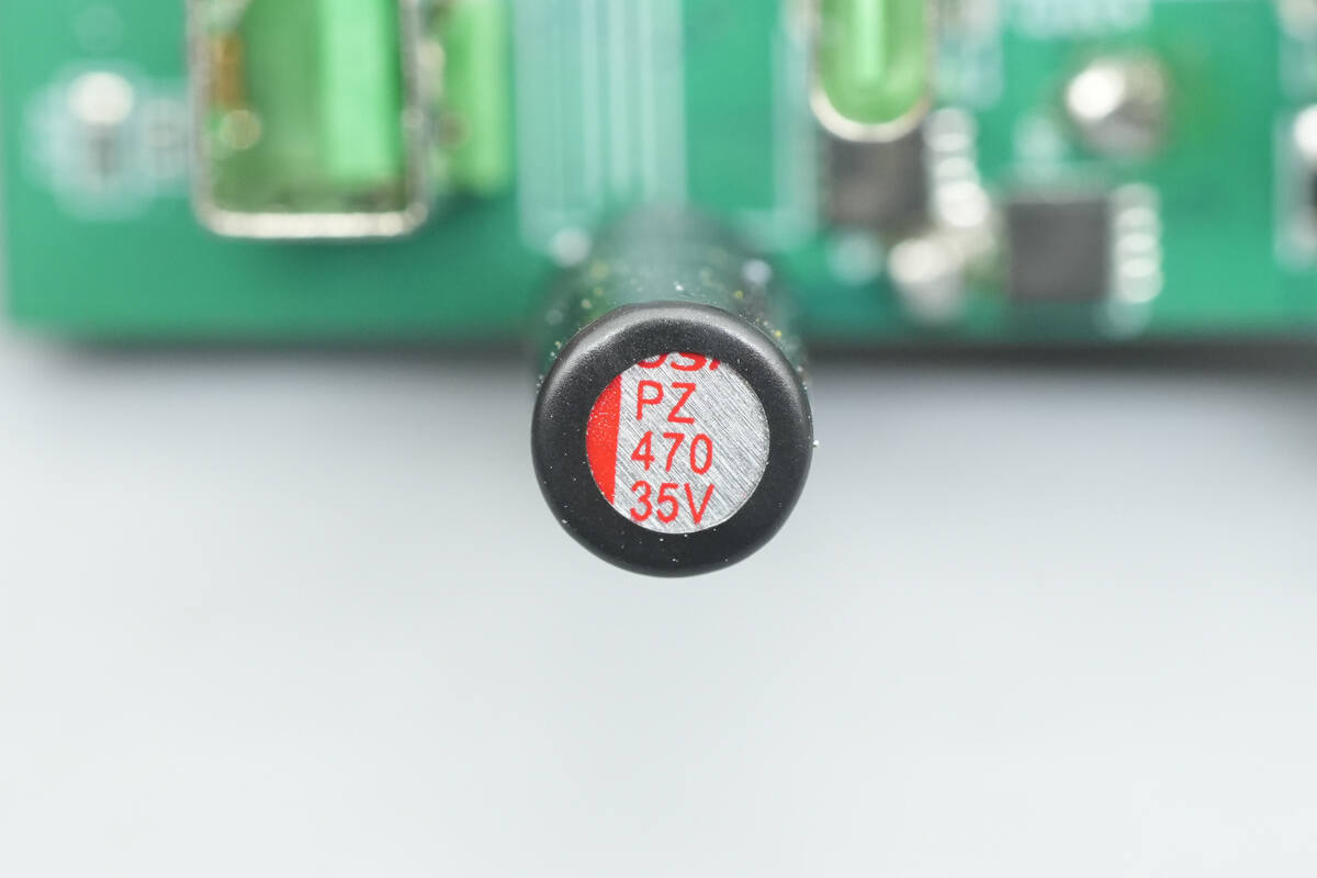
The solid capacitor for output filtering is also from JSH, rated at 35 V and 470 μF.
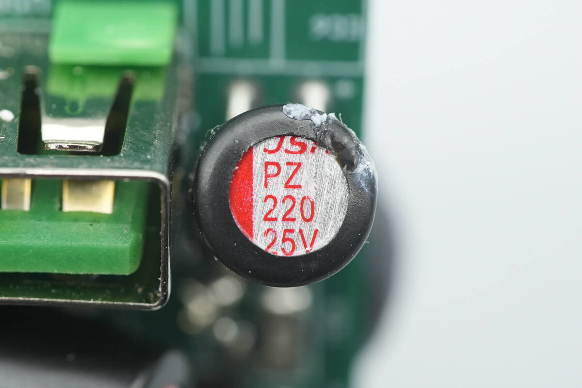
The other solid capacitor for output filtering is also from JSH, rated at 25 V and 220 μF.
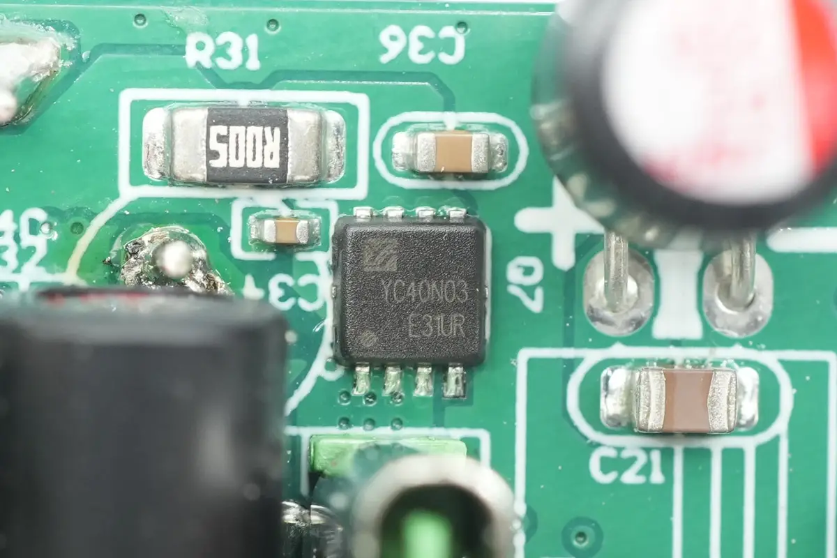
The VBUS MOSFET for the USB-C3 port is from YouCrystal, model YC40N03ADE, NMOS, with a voltage rating of 30 V and an on-resistance of 8.5 mΩ, housed in a PDFN 3×3 package.
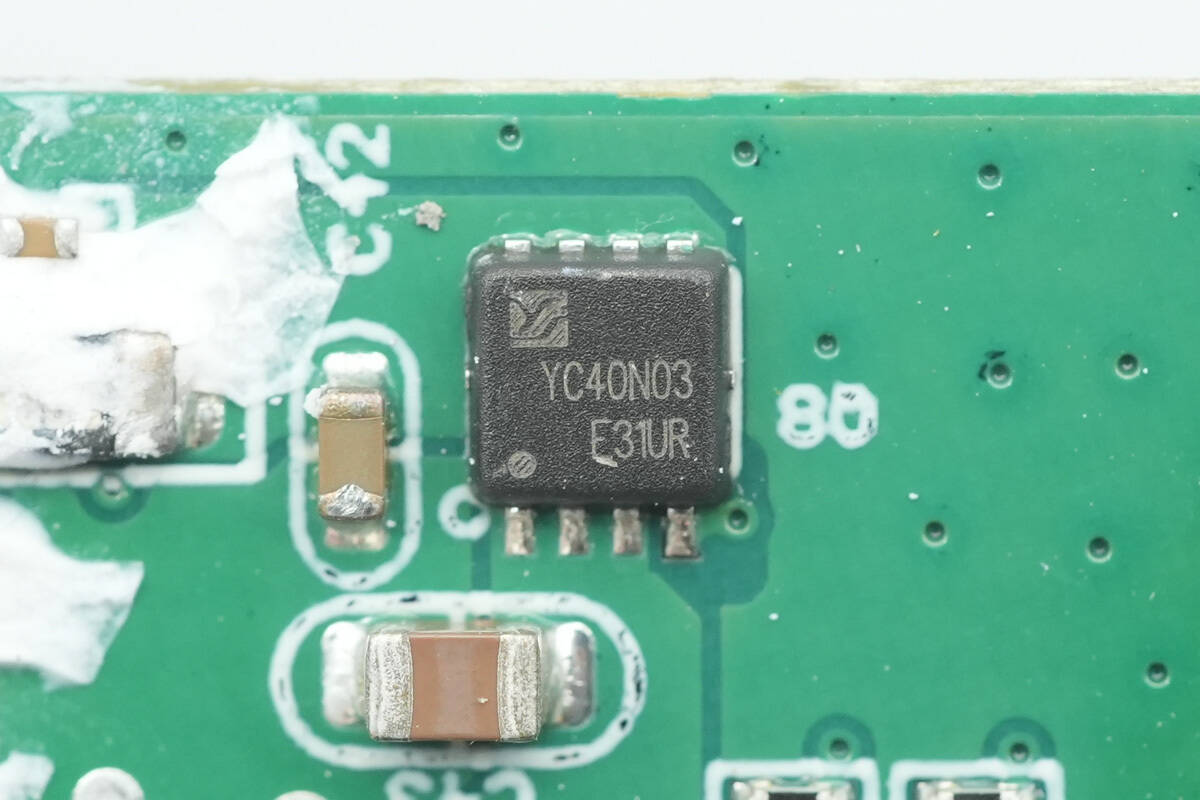
The VBUS MOSFET for the USB-A port is also YouCrystal YC40N03ADE.
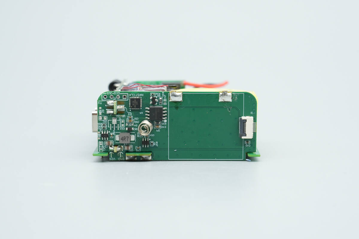
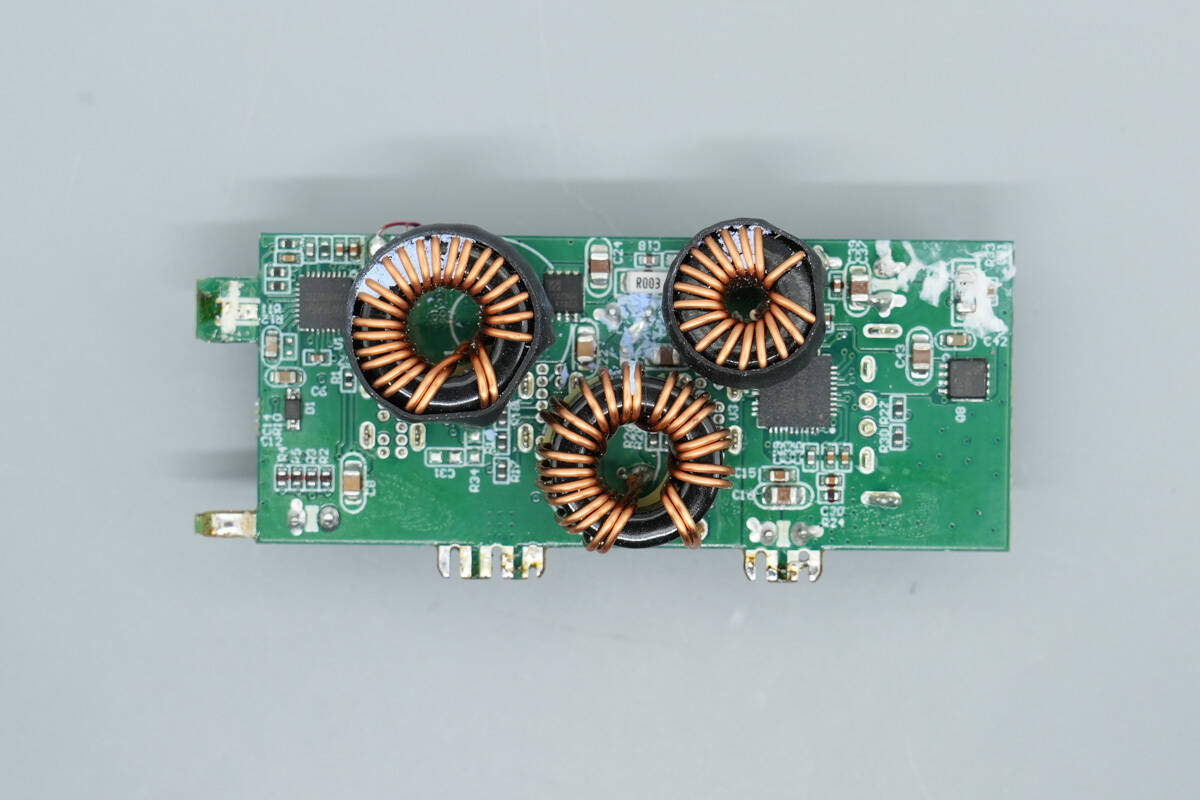
On the other side of the module, a screen control PCB is soldered. The front side features an MCU, memory, a synchronous buck converter, a buck inductor, a touch-sensing chip, and other components.
Remove the PCB; the other side has no components.
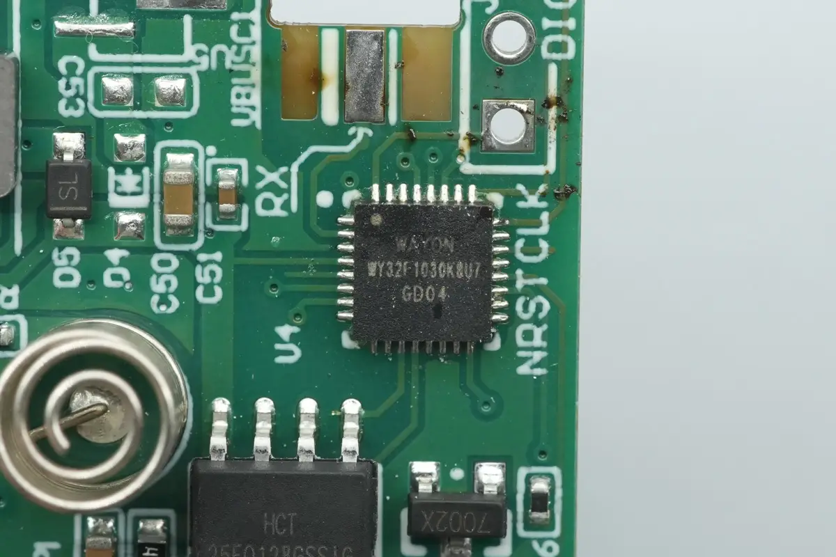
The WAYON WY32F1030 is a 32-bit MCU, housed in a QFN32 package.
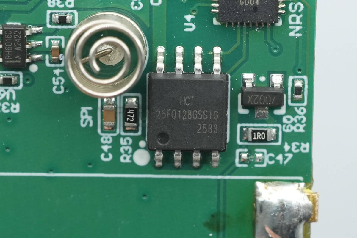
The memory is from HCT, model 25FQ128GSSIG, in an SOP8 package.
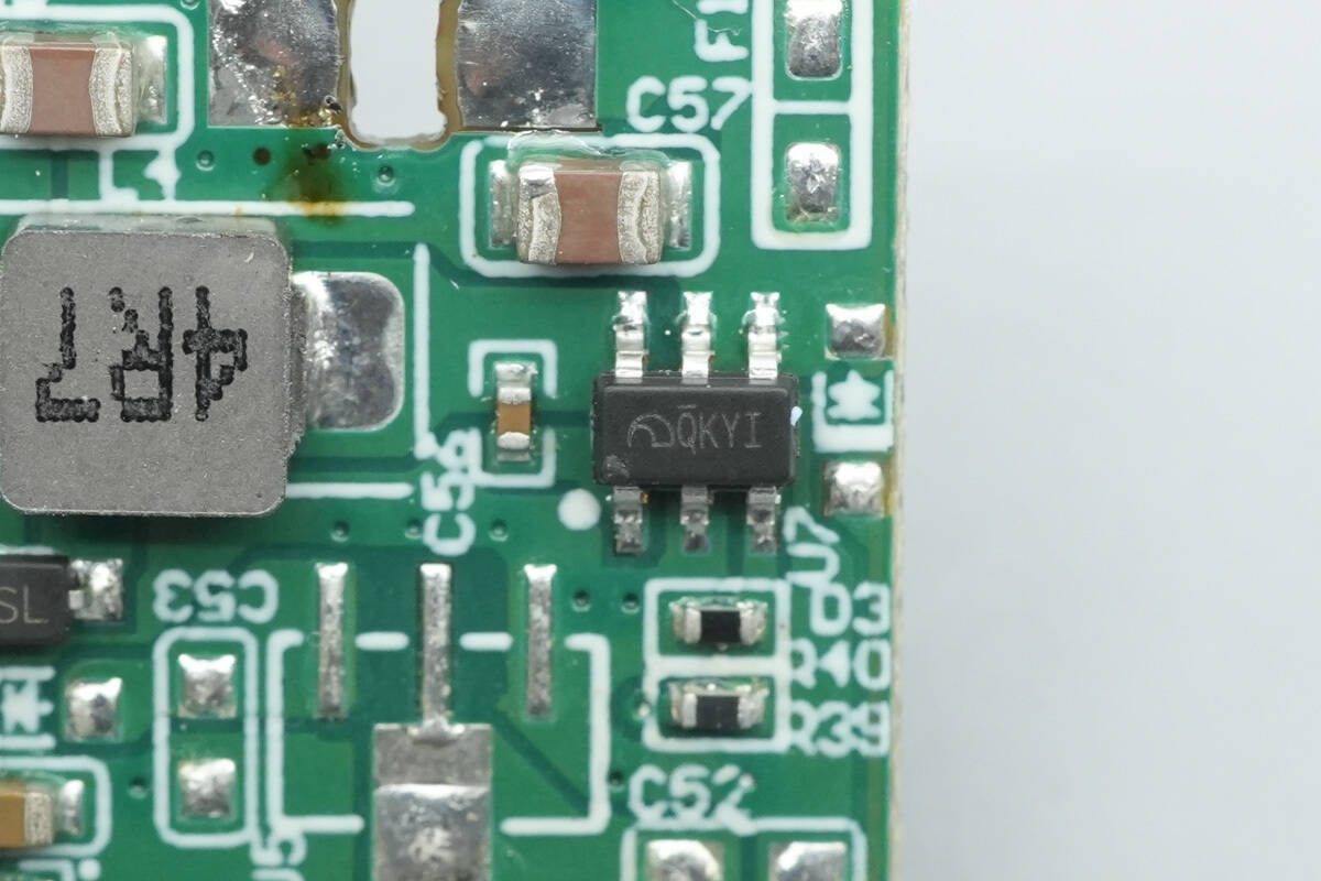
The synchronous buck converter used for a step-down power supply is marked with QKYI.
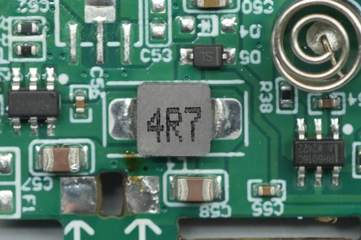
Close-up of the paired 4.7 μH buck inductor.
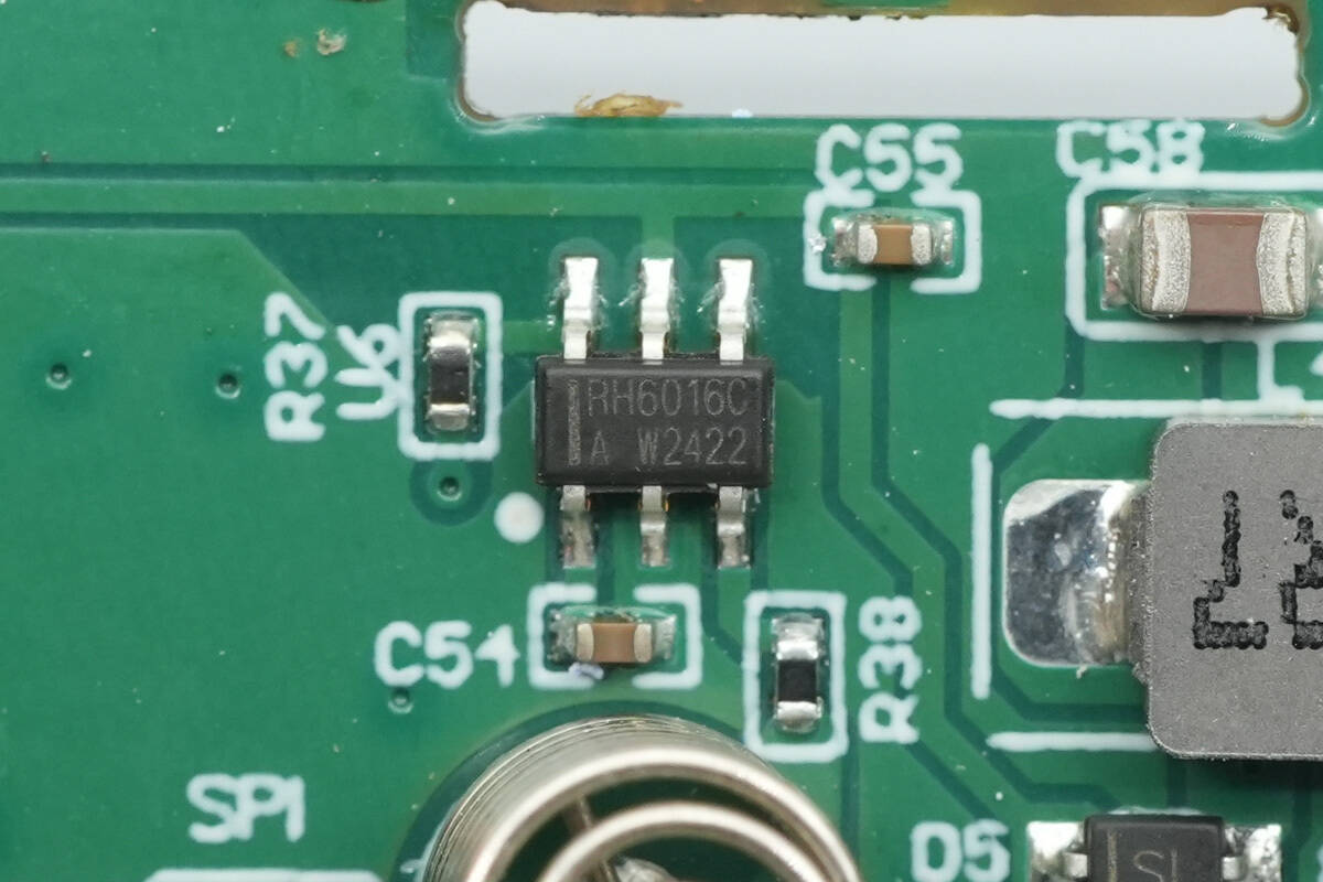
The touch-sensing chip is from Ronghe, model RH6016C. It is a single-channel capacitive touch sensor with a built-in voltage regulator, featuring high-precision regulation, power-on reset, and low-voltage reset, as well as hardware debounce and other anti-interference measures.
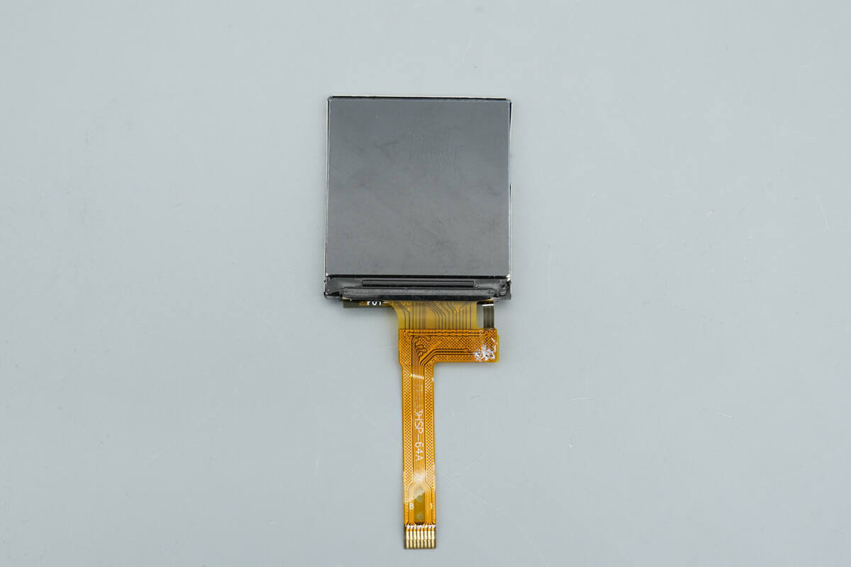
Close-up of the screen.

Well, those are all components of the Highsay C1 Pro 140W Ultra Charger.
Summary of ChargerLAB

Here is the component list of the Highsay C1 Pro 140W Ultra Charger for your convenience.
The equipped screen can display total power, individual port power, temperature, and charging status at a glance. It features simple touch-key operation and supports both landscape and portrait orientations. The device has three USB-C ports and one USB-A port, compatible with fast-charging protocols such as QC, SCP, PD 3.1, and PPS, making it well-suited for devices from Apple, Xiaomi, Samsung, and other brands. It can simultaneously charge laptops, tablets, smartphones, and headphones, meeting multi-device charging needs in a single unit.
After taking it apart, we found that it uses a single-stage high-PF power design with Kiwi Instruments KP2815 + KP4060, paired with Innoscience INN650D080B GaN power device. The output consists of three independent DC-DC secondary buck circuits using iSmartWare SW3566H and SW3537. The modules are filled with adhesive and covered with thermal pads, with heat sinks assisting in heat dissipation. A thermistor is included for temperature monitoring, and combined with the intelligent display, it provides safe and visualized operation.
Related Articles:
1. Teardown of Belkin BoostCharge Pro 140W Braided USB-C to Dual USB-C Cable (CAC004)
2. Teardown of Baseus T-Space 3rd Generation 60W GaN Charger Dock for Tesla (BS-TS017)
3. Teardown of Anker Prime 14-in-1 Docking Station (A83B3) – Black Myth: Wukong Edition