Introduction
We obtained DJI’s newly released Osmo Mobile 8 smartphone gimbal. This gimbal integrates an extension rod and a tripod into a single design, supports 360° unlimited horizontal rotation, is compatible with Apple DockKit, and supports HarmonyOS intelligent tracking. An extension rod is built into the gimbal handle, while an integrated tripod is located at the bottom of the handle, making it suitable for both handheld and desktop use.
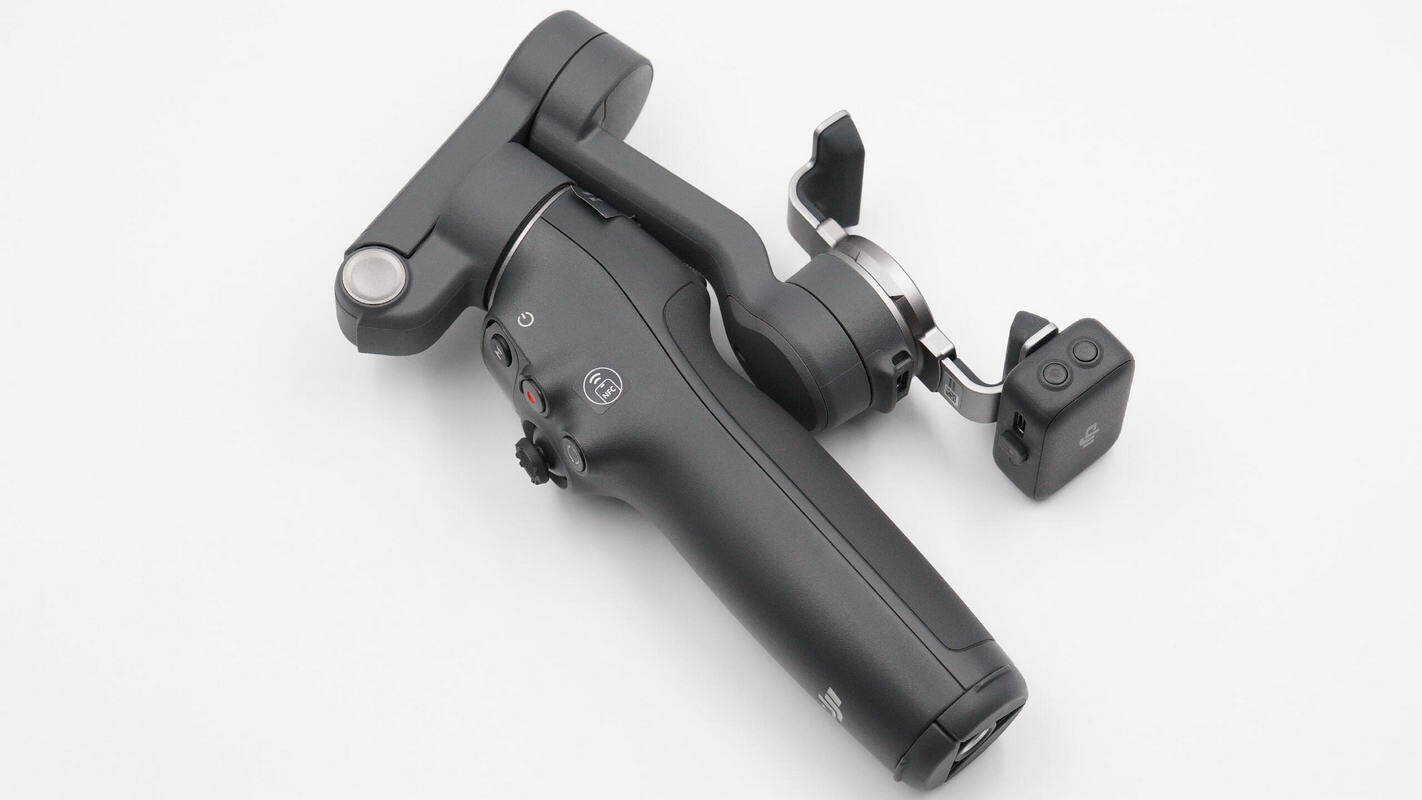
The gimbal features a three-axis design, supporting pan, tilt, and roll movements. It adopts DJI’s seventh-generation stabilization technology to achieve lossless image stabilization, and further supports switching between low-angle and high/low shooting positions. It also supports one-button switching between front and rear cameras, delivering high-definition image quality. The gimbal can be used with magnetic quick-release mounting pads, the Mic Mini transmitter, a handheld tripod, and tracking kits.
The gimbal charges via a USB-C port and is equipped with a built-in 3350mAh battery, providing up to 10 hours of battery life and supporting smartphone charging. The gimbal handle is equipped with a joystick and a control wheel, significantly enhancing the operating experience. Below, we present a teardown of the DJI Osmo Mobile 8 smartphone gimbal to take a closer look at its internal design and components.
Product Appearance

The front of the packaging box is printed with the model, product name, and usage scenarios.
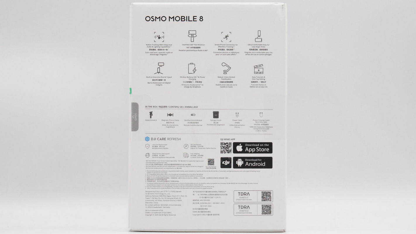
The back of the packaging features key selling points and manufacturer information.
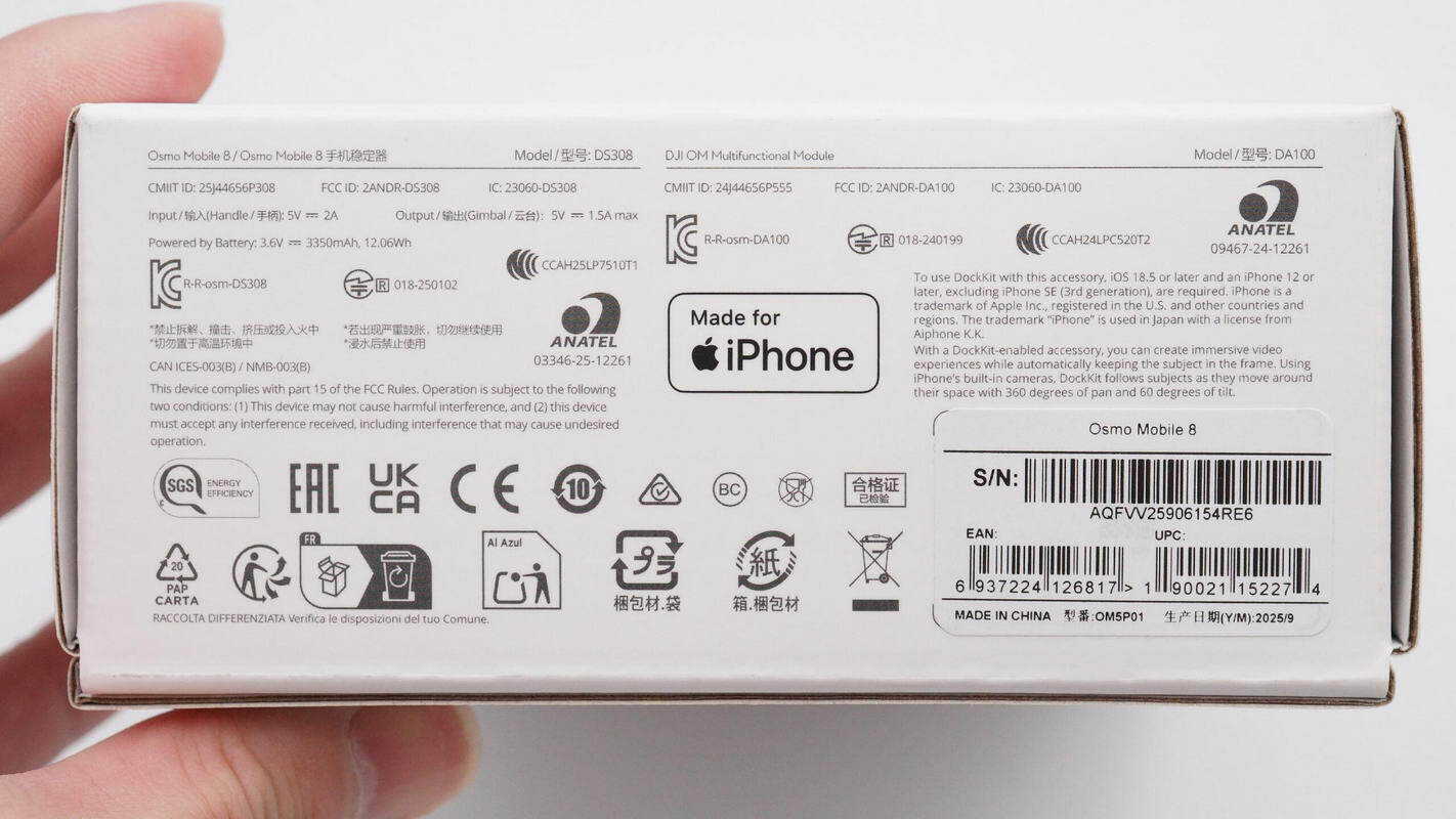
The bottom is printed with product information, the MFi certification mark, and serial number details.
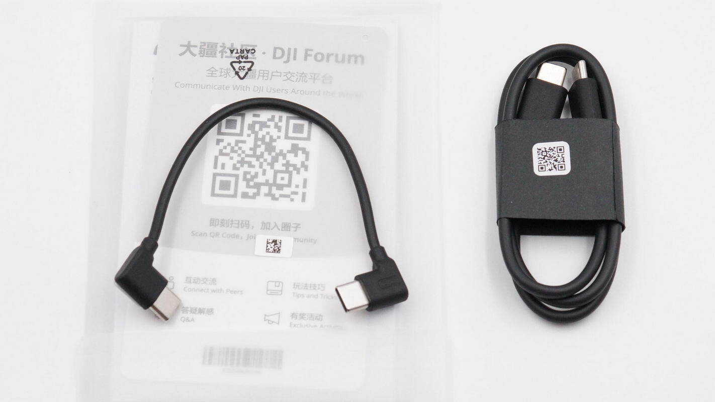
Inside the package, one long and one short USB-C cable are included.

The gimbal is packaged in a protective carrying pouch.
An overview of the folded storage configuration, with the magnetic phone clamp and the DJI OM Multifunctional Tracking Module installed.
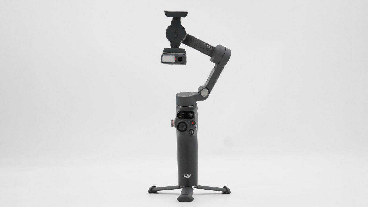
An overview of the gimbal with the built-in tripod at the base unfolded.
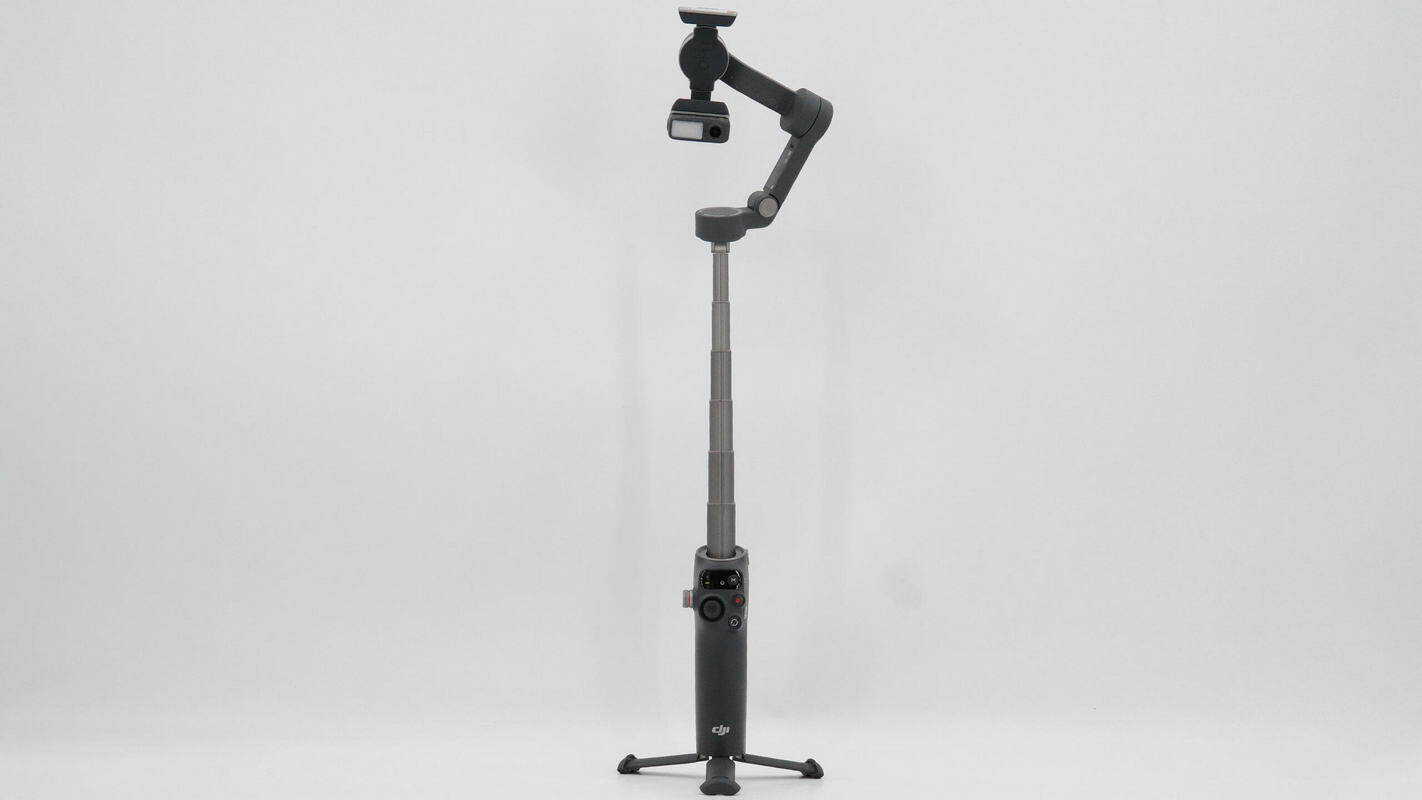
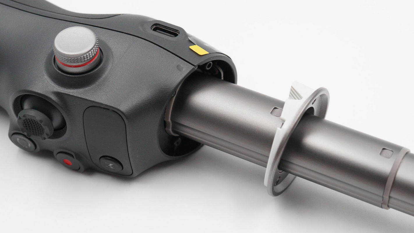
An overview with the built-in extension rod pulled out and the bottom tripod deployed.
The bottom features mounting screw holes.
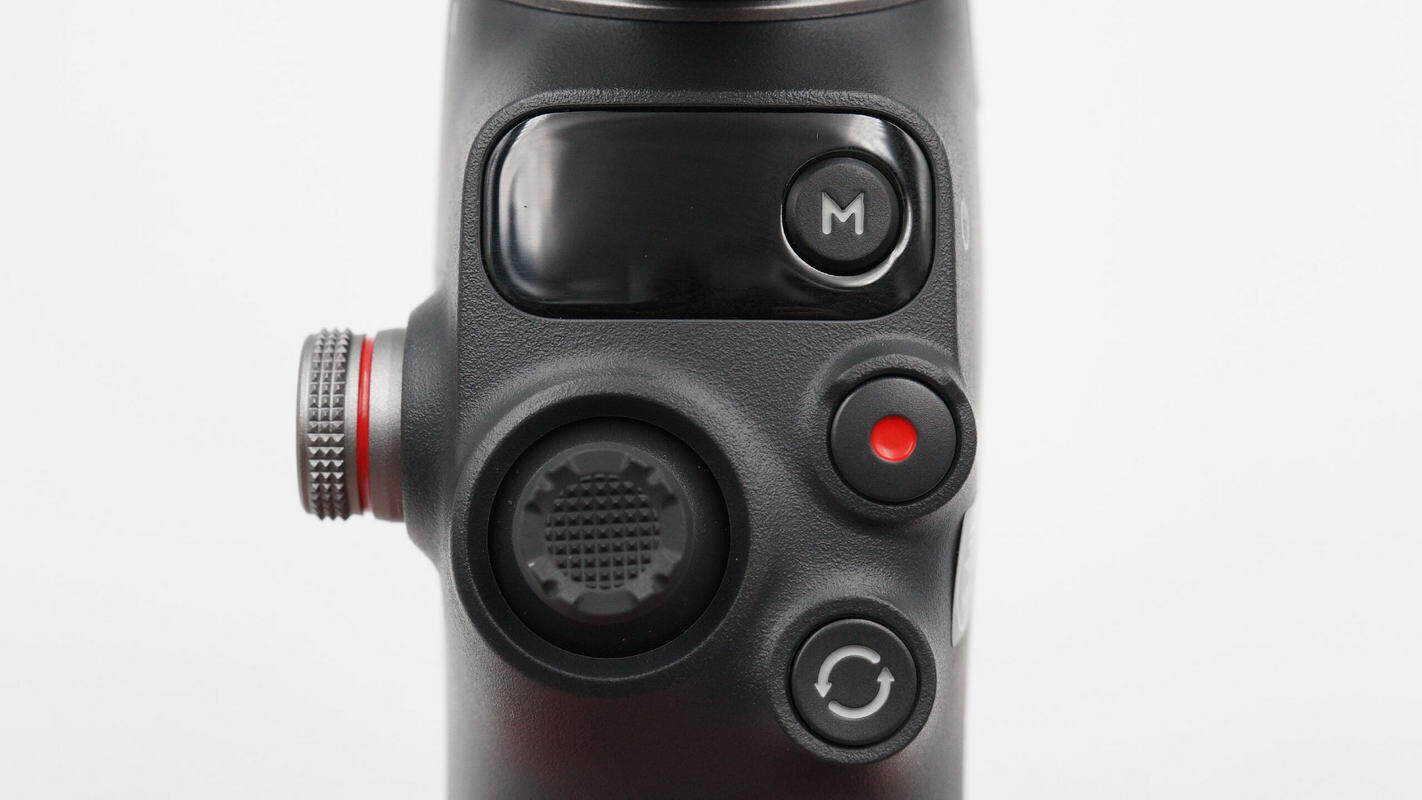
The front of the gimbal features a control panel, indicator lights, a joystick, a mode switch button, a shutter button, and a power button.

The joystick has a raised texture for easier positioning and improved grip.
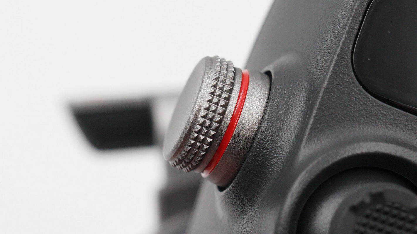
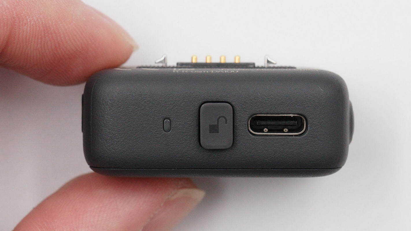
A control wheel is located on the left side.
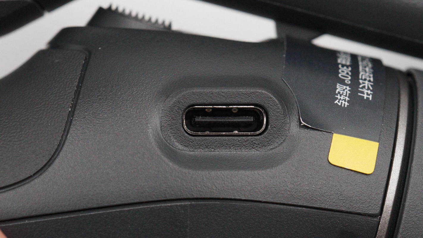
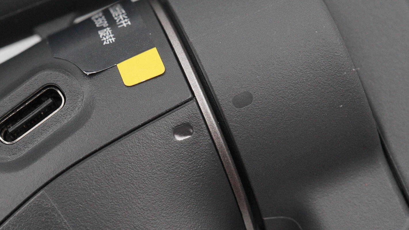
A USB-C charging port is also located on the left side.
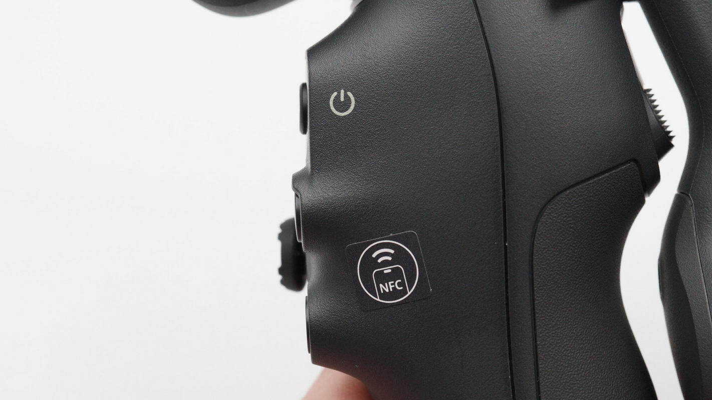
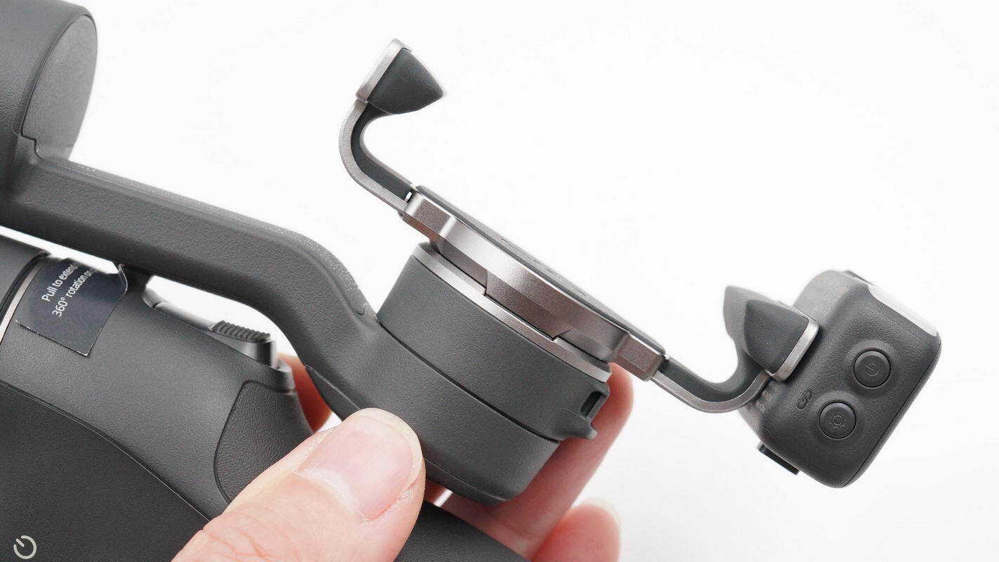
An NFC tag is affixed to the right side.
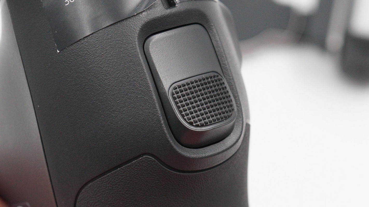
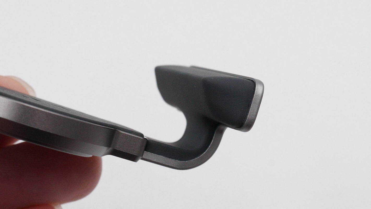
A trigger button is located on the front of the gimbal.
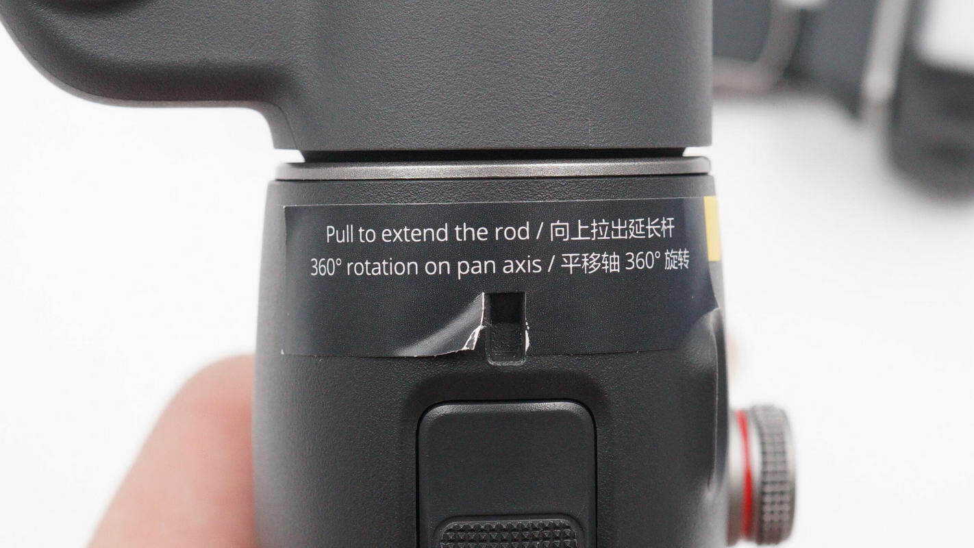
Above the trigger button is a positioning groove with an instructional sticker attached.
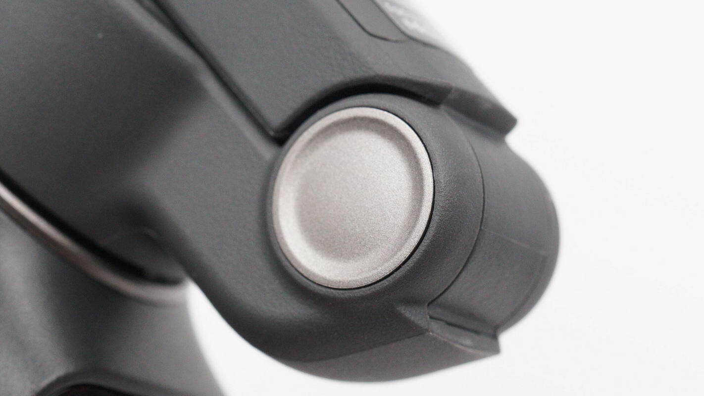
Close-up of the side pan-axis positioning mark.
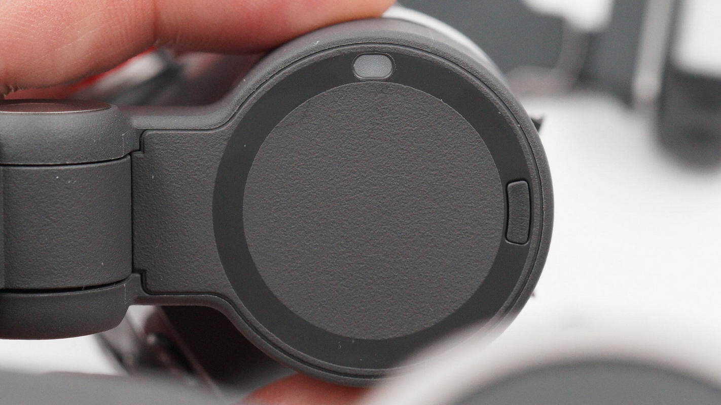
A function status indicator light is located on the top.
The folding axis is made of metal.
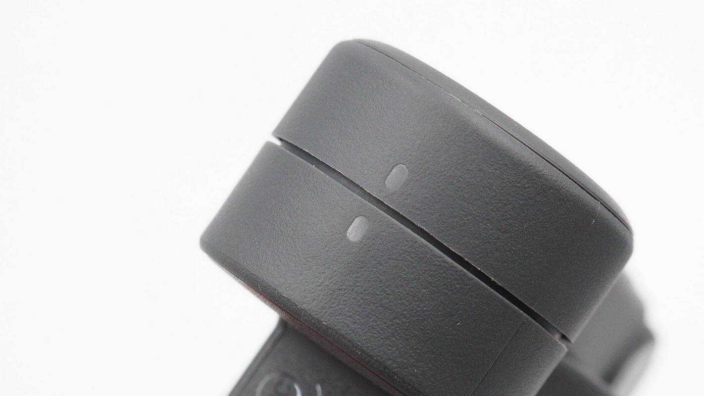
Close-up of the side positioning mark.

Product information is printed on the inner side of the axis wall.
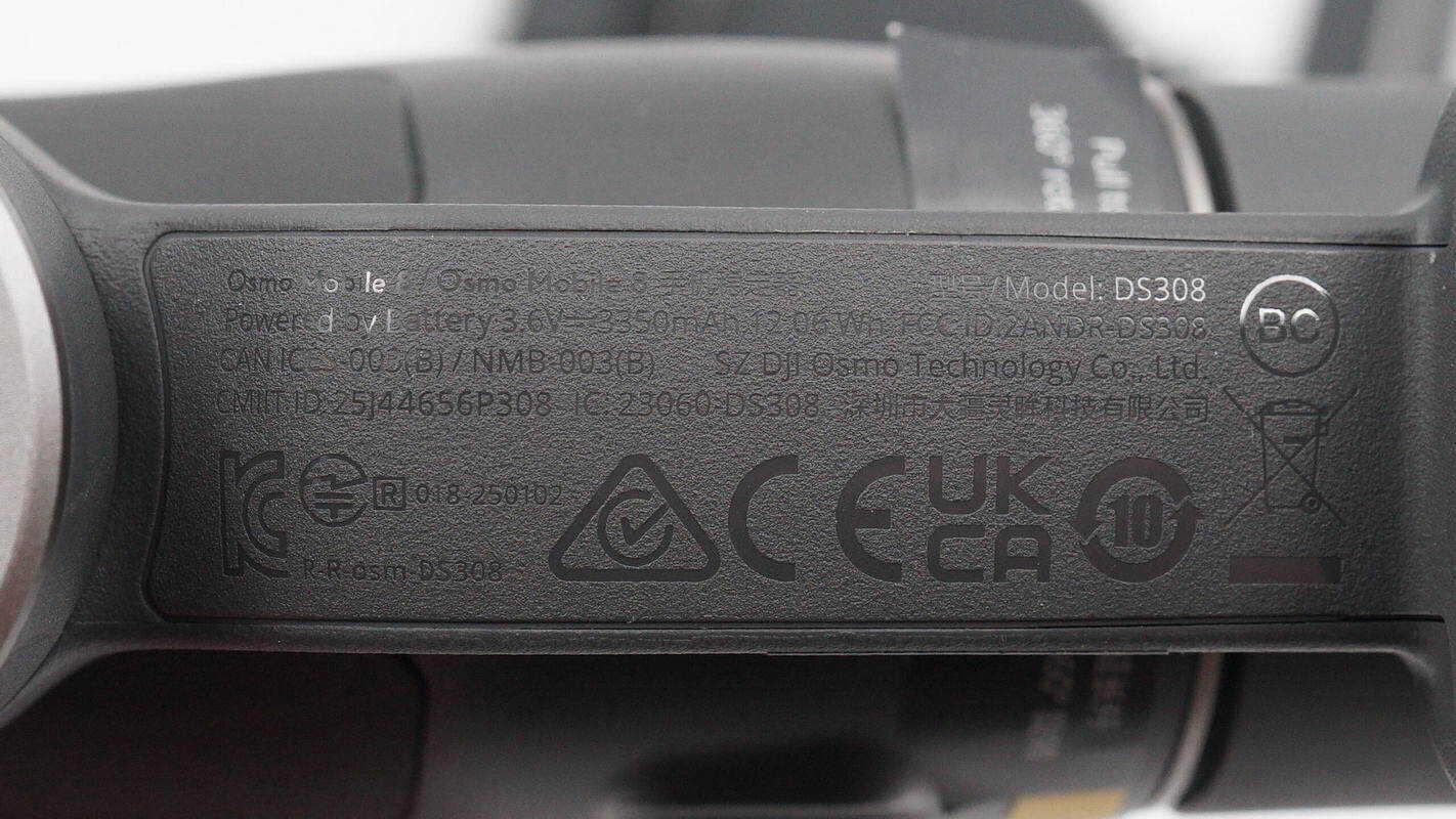
The battery is rated at 3.6 V⎓3350 mAh, 12.06 Wh.
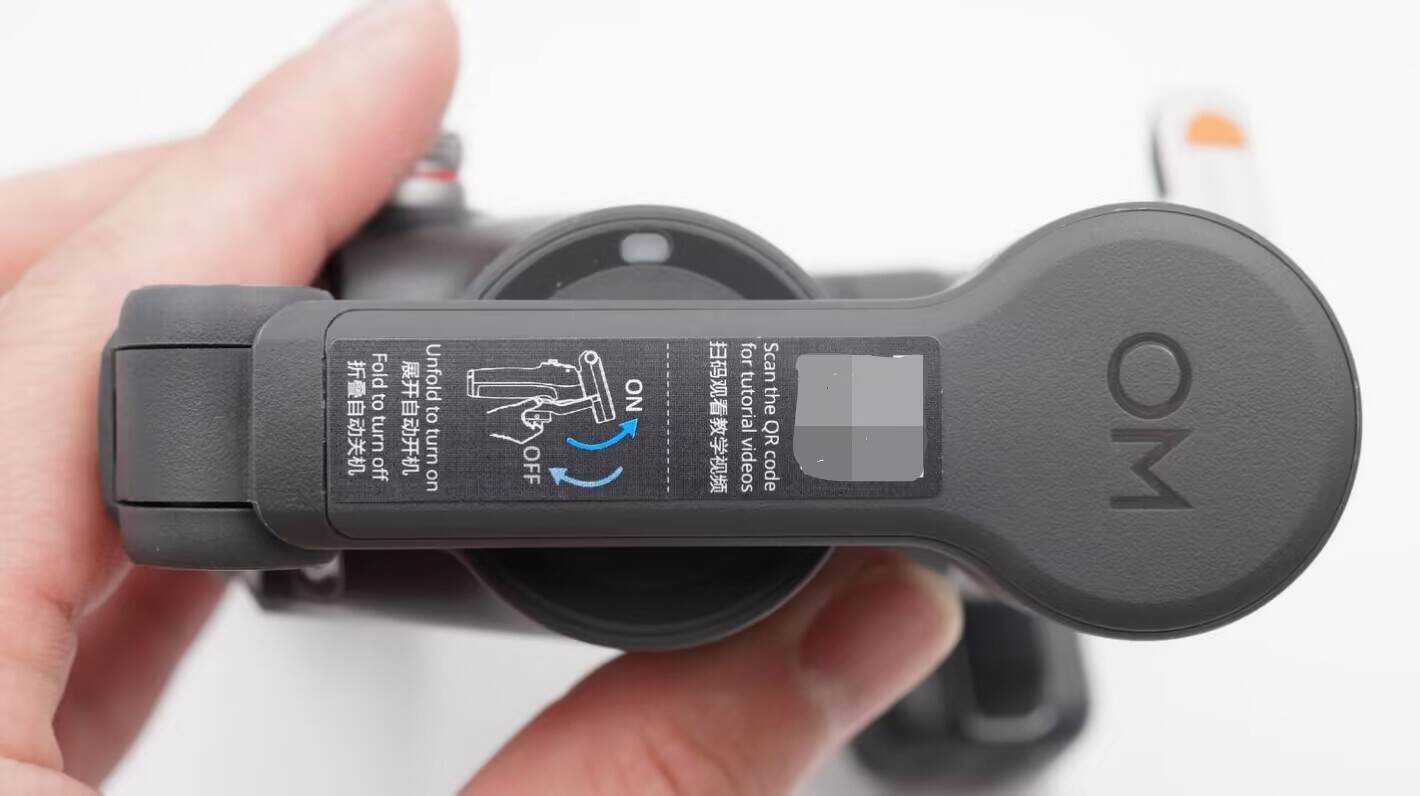
A usage instruction sticker is affixed to the outer side of the axis wall.
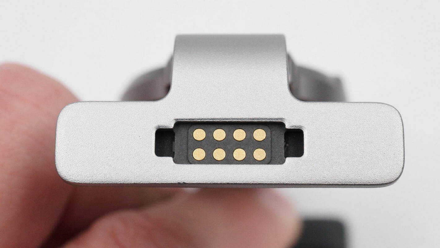
The phone clamp is secured using a magnetic attachment.
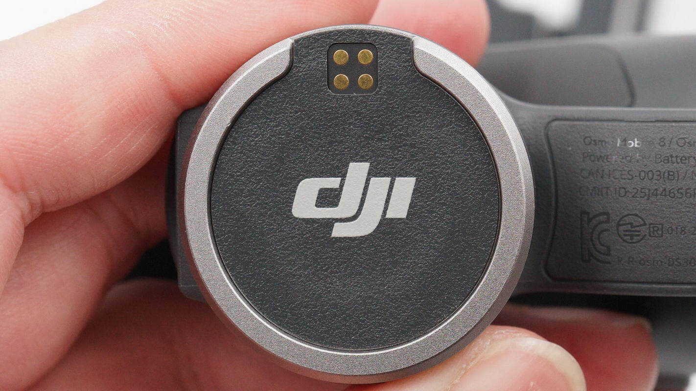
Connection contact points are provided.
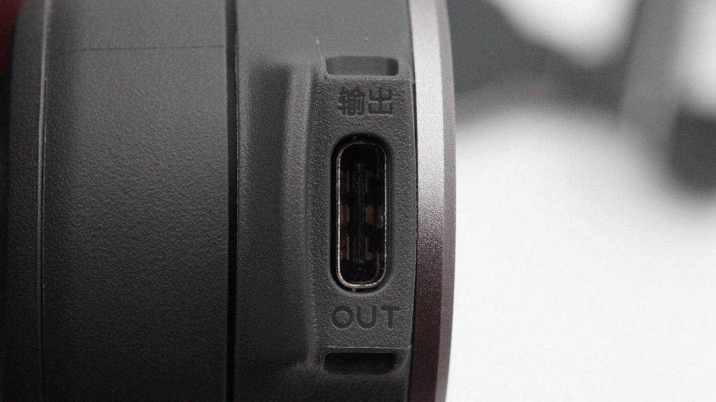
A USB-C output port is located on the side.
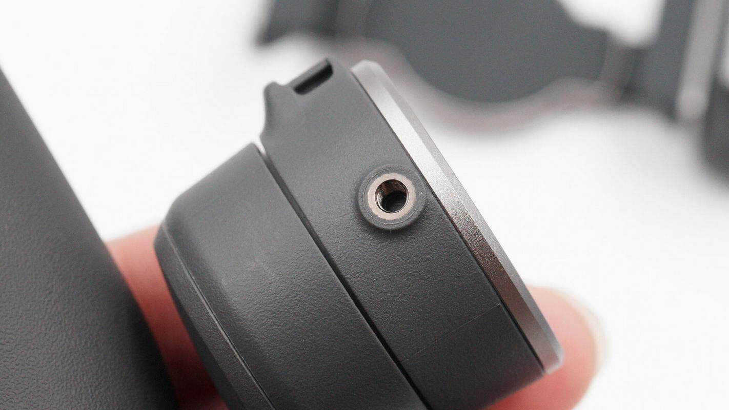
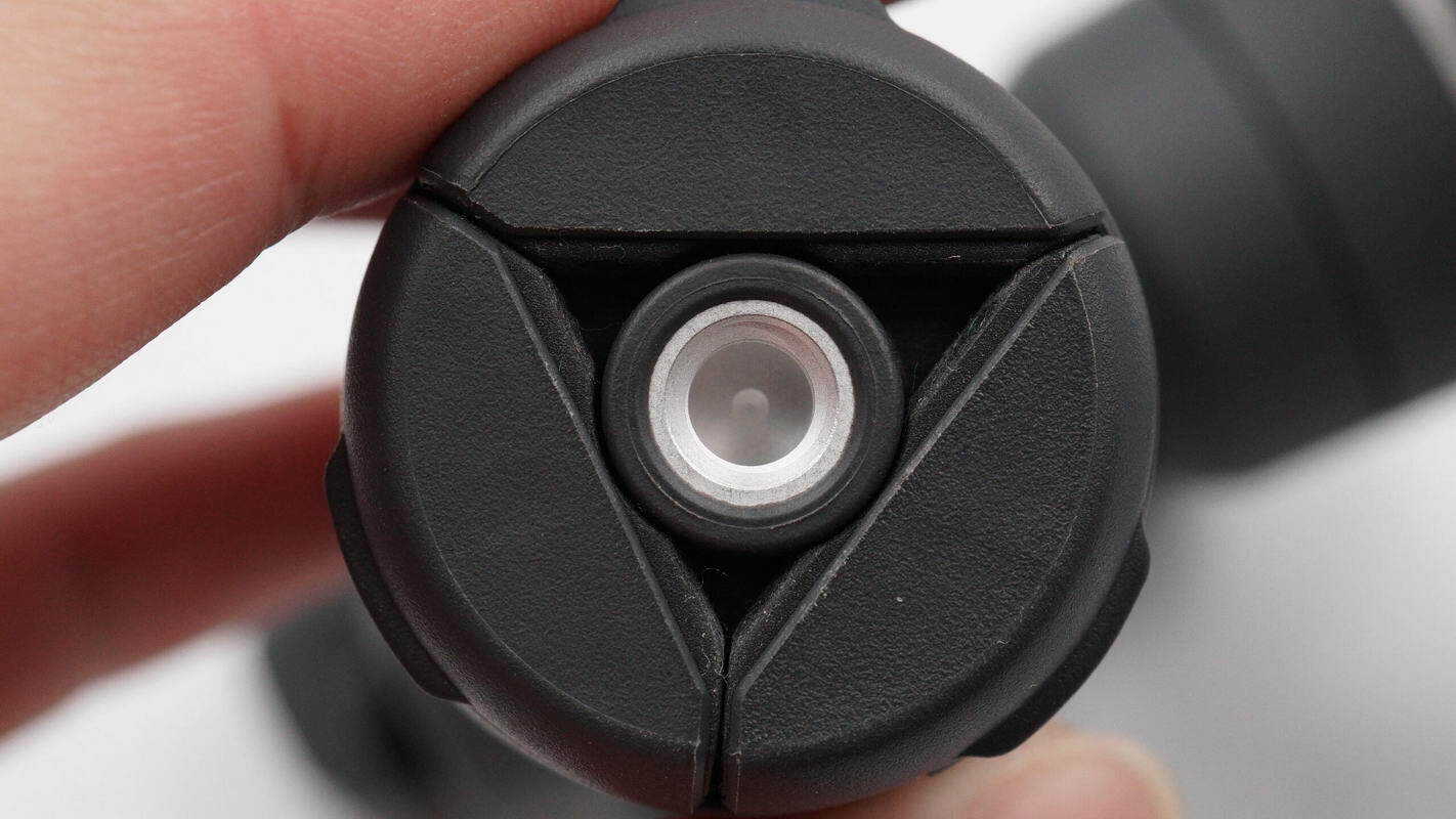
Close-up of the counterweight mounting hole.
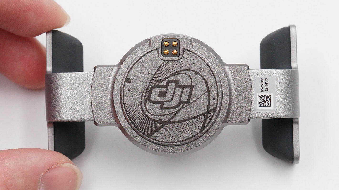
The back of the magnetic phone mount features Pogo pins.
The inner side of the phone clamp arm is equipped with angled soft rubber pads to secure and protect the phone.
Connection contact points are located on the side.
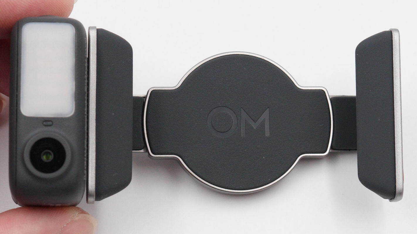
The DJI OM Multifunctional Tracking Module attaches magnetically to the side of the magnetic phone mount and is secured with a latch.
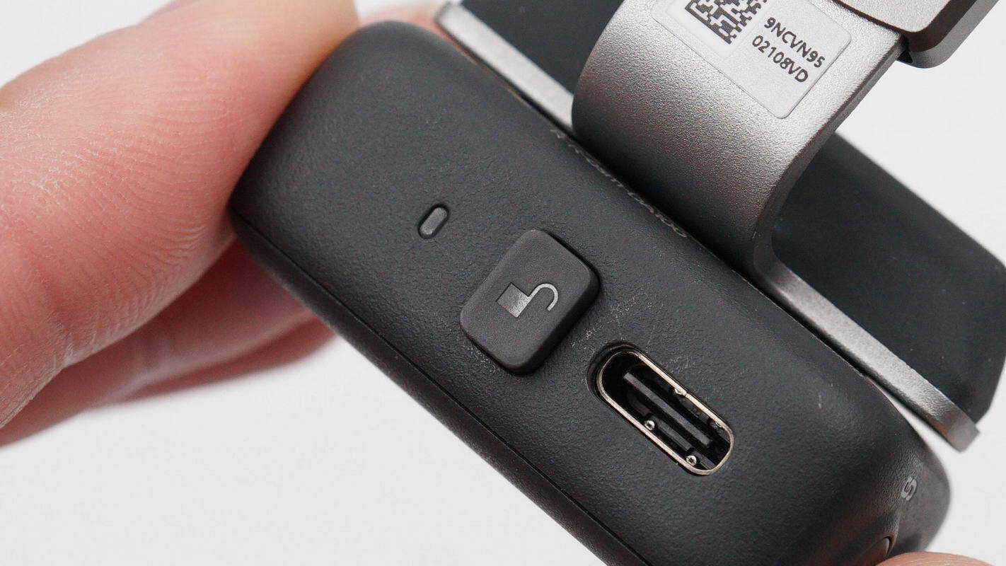
The side of the module features a lock button and a USB-C port.
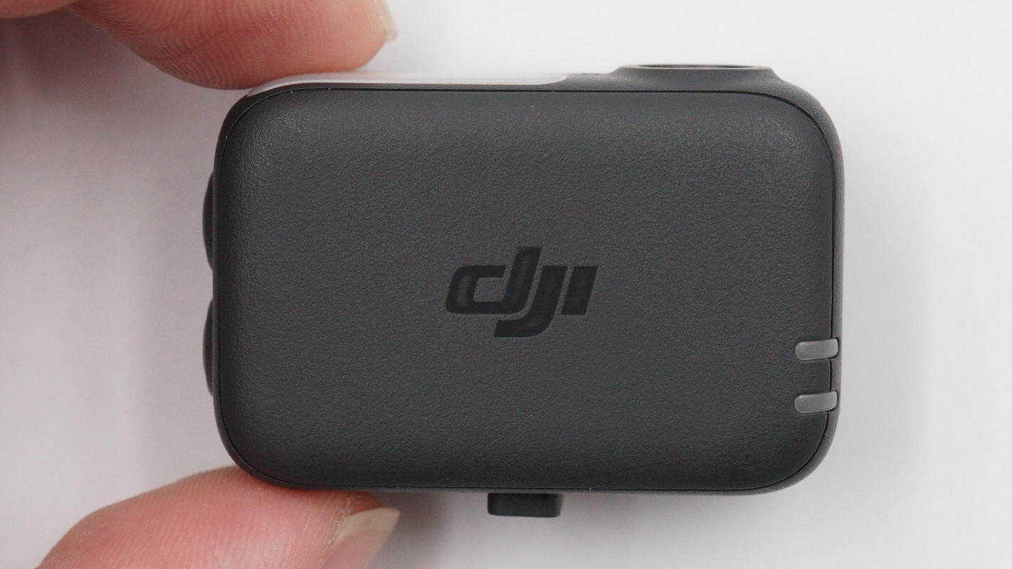
The front of the module is printed with the DJI logo.
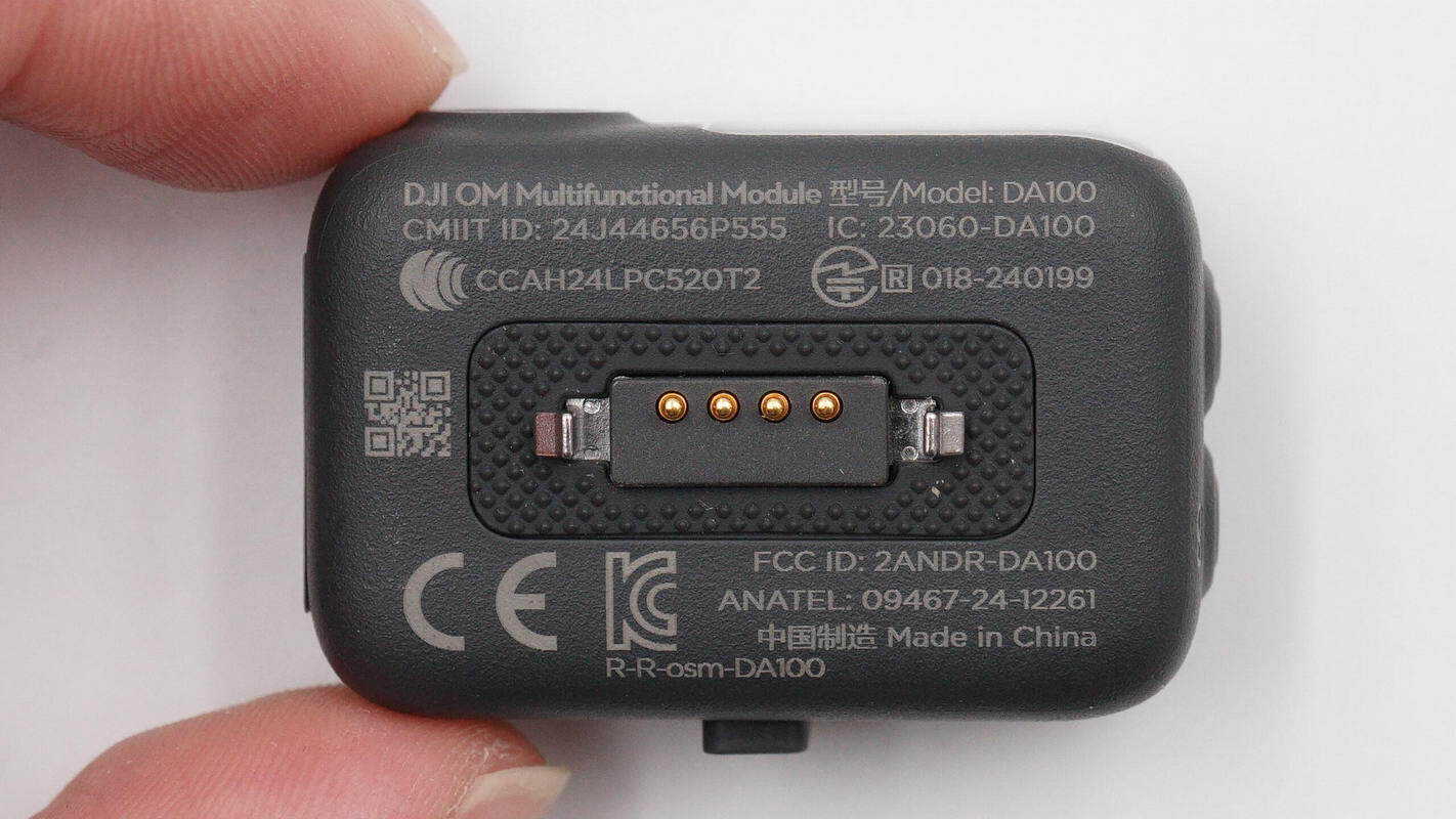
The back of the module features a connector.
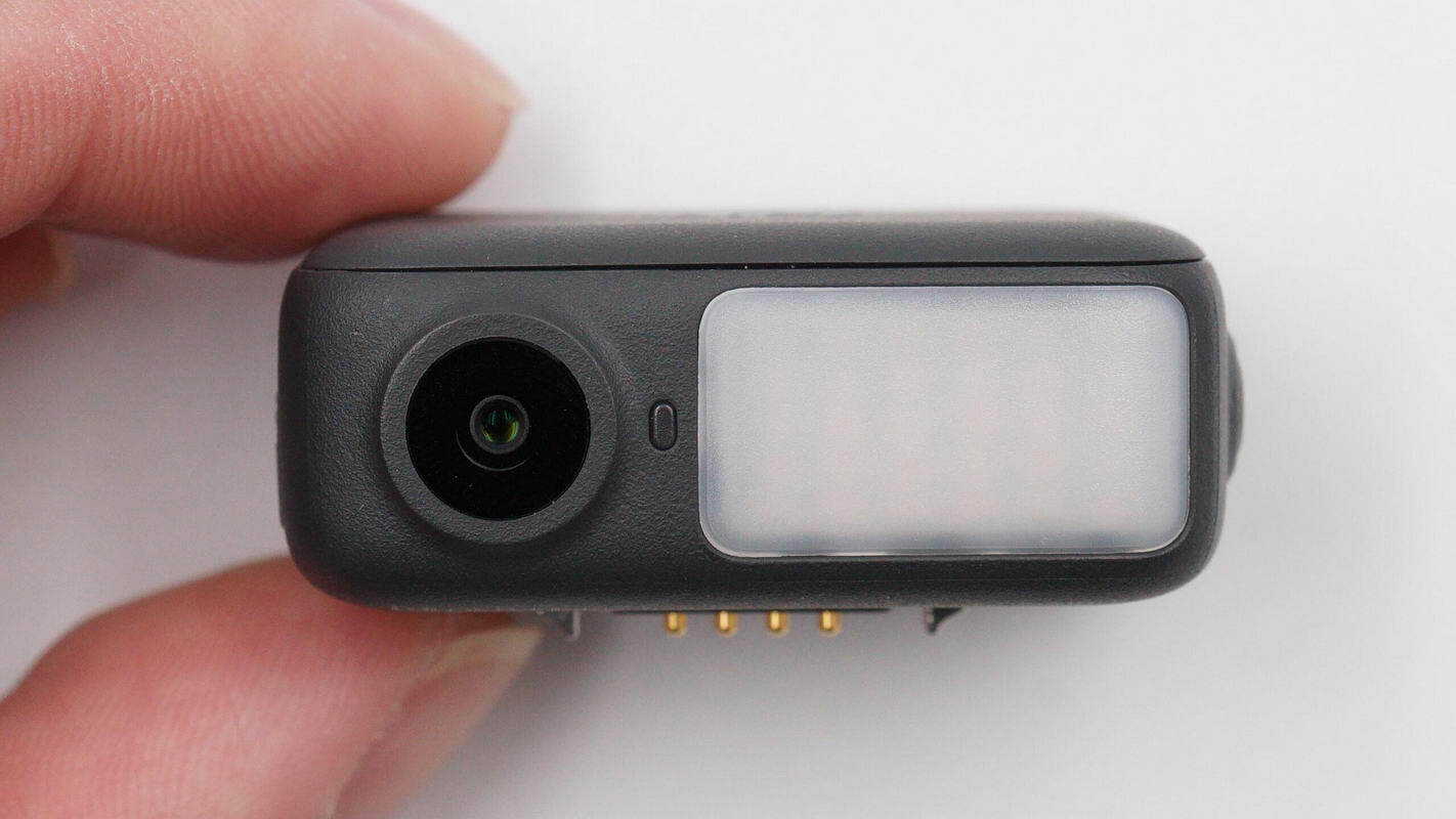
The side of the module is equipped with a tracking camera, a recording status indicator light, and a fill light.
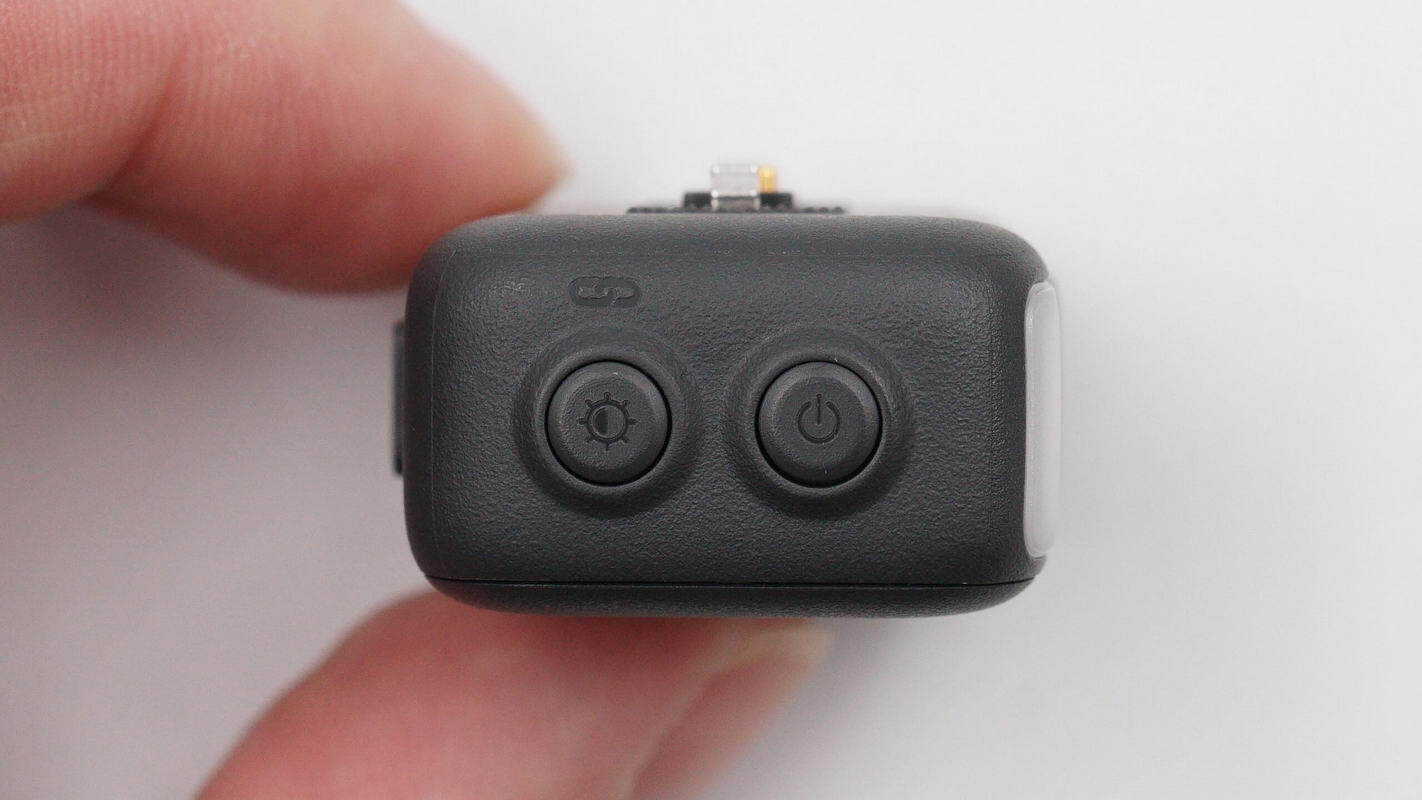
The opposite side features a brightness control button and a power button.
The other side features a recording status indicator light, an unlock button, and a USB-C port.
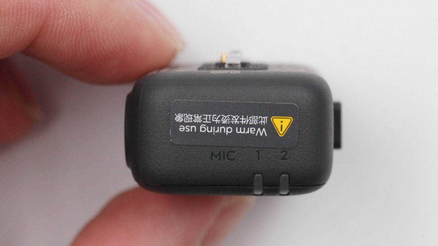
The side features a status indicator light for the wireless microphone.

The module’s Pogo pin contacts are flanked by securing latches on both sides.
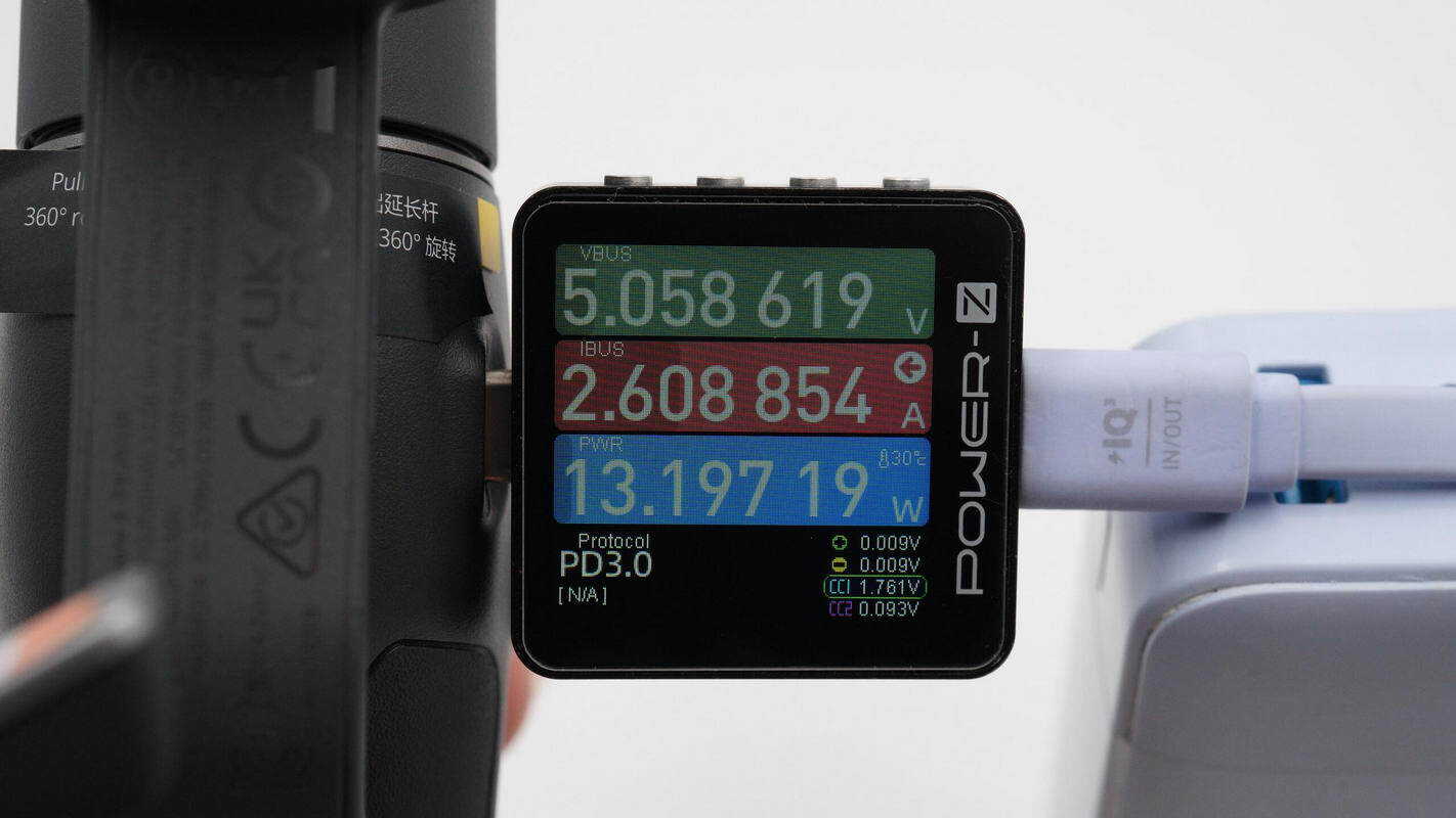
To charge the gimbal, the input voltage is about 5.06 V, the input current is about 2.61 A, and the charging power is about 13.2 W.
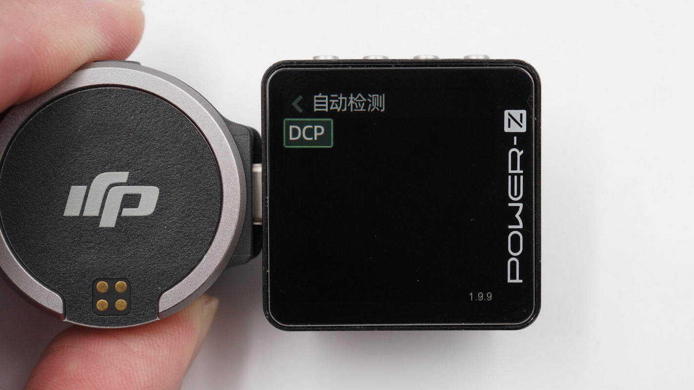
Testing shows that the gimbal’s output supports only the DCP charging protocol.
Teardown
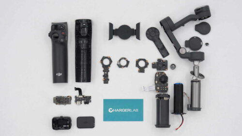
Next, let's take it apart to see its internal components and structure.
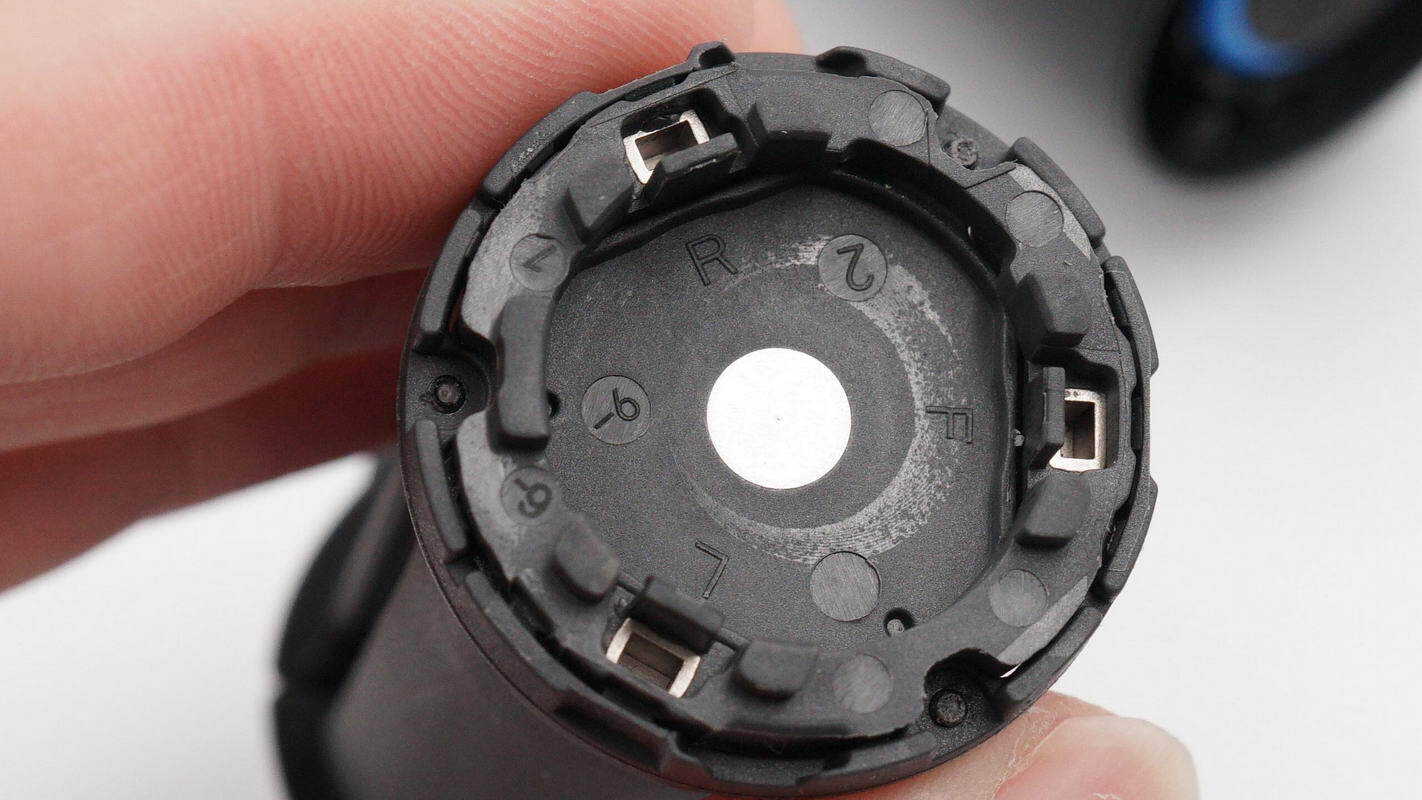
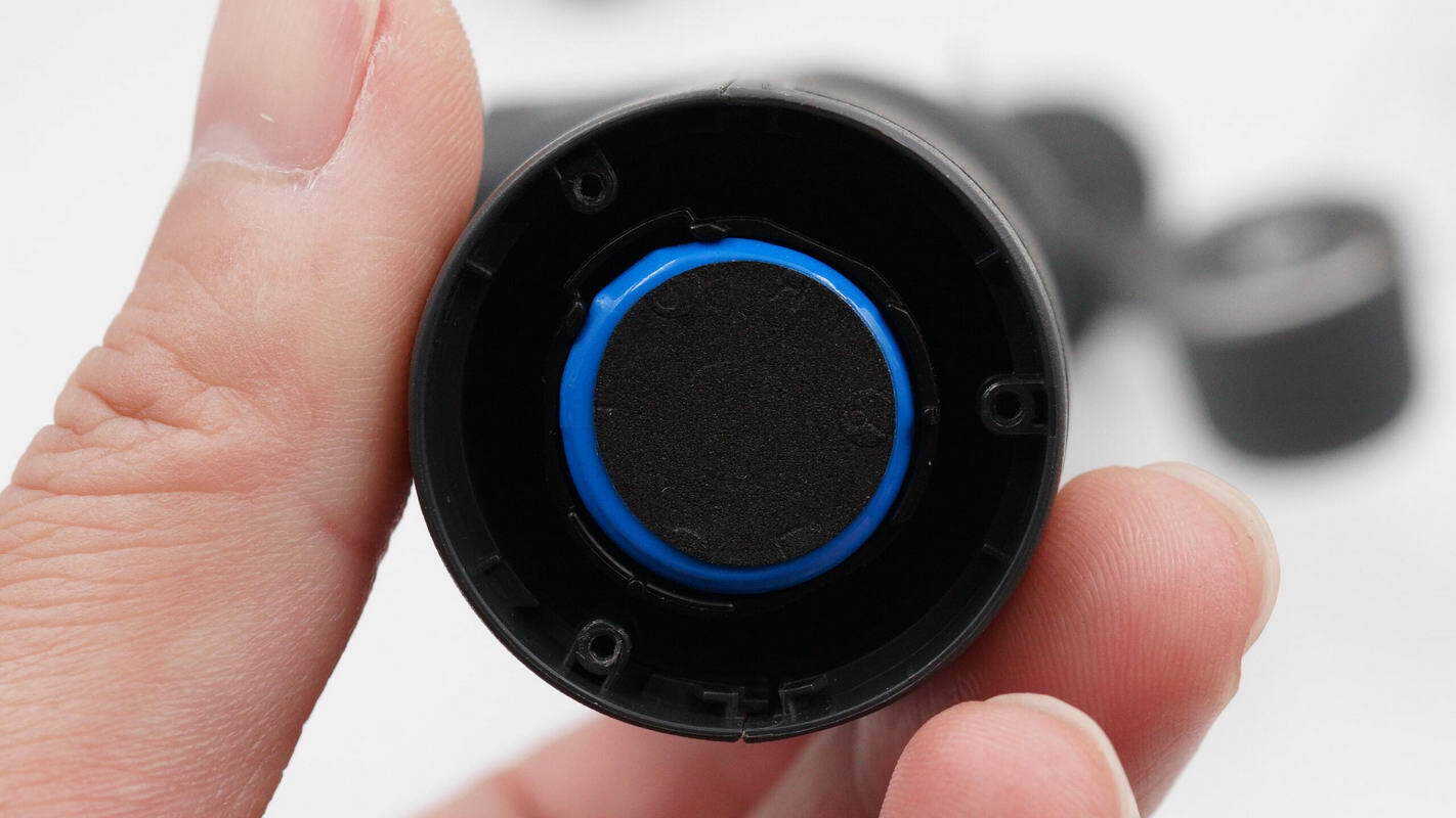
By unscrewing the mounting screws, the built-in tripod at the bottom can be removed.
The tripod uses a metal hinge axis.
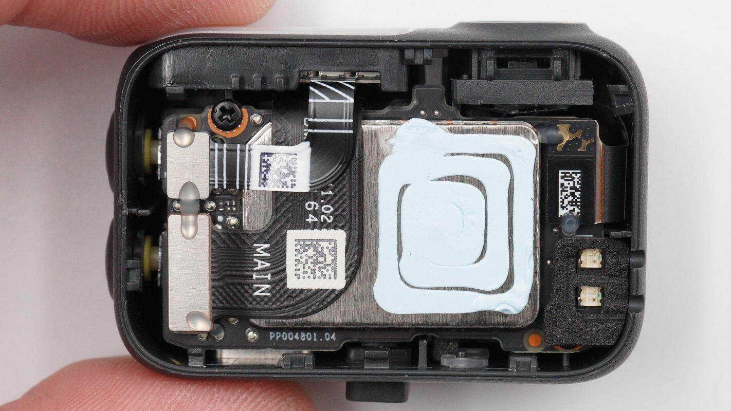
The battery is wrapped in a blue plastic casing, with cushioning foam attached to the bottom.
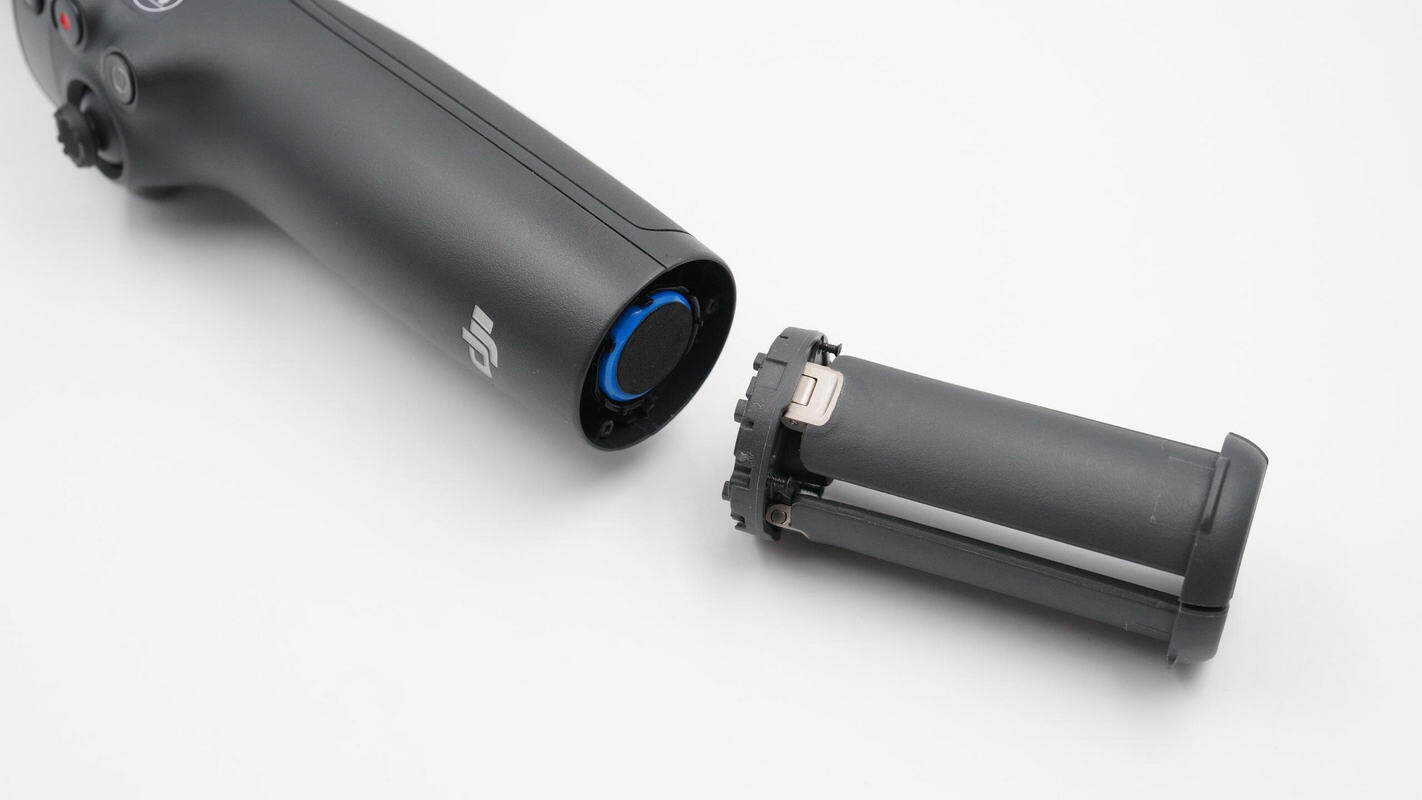
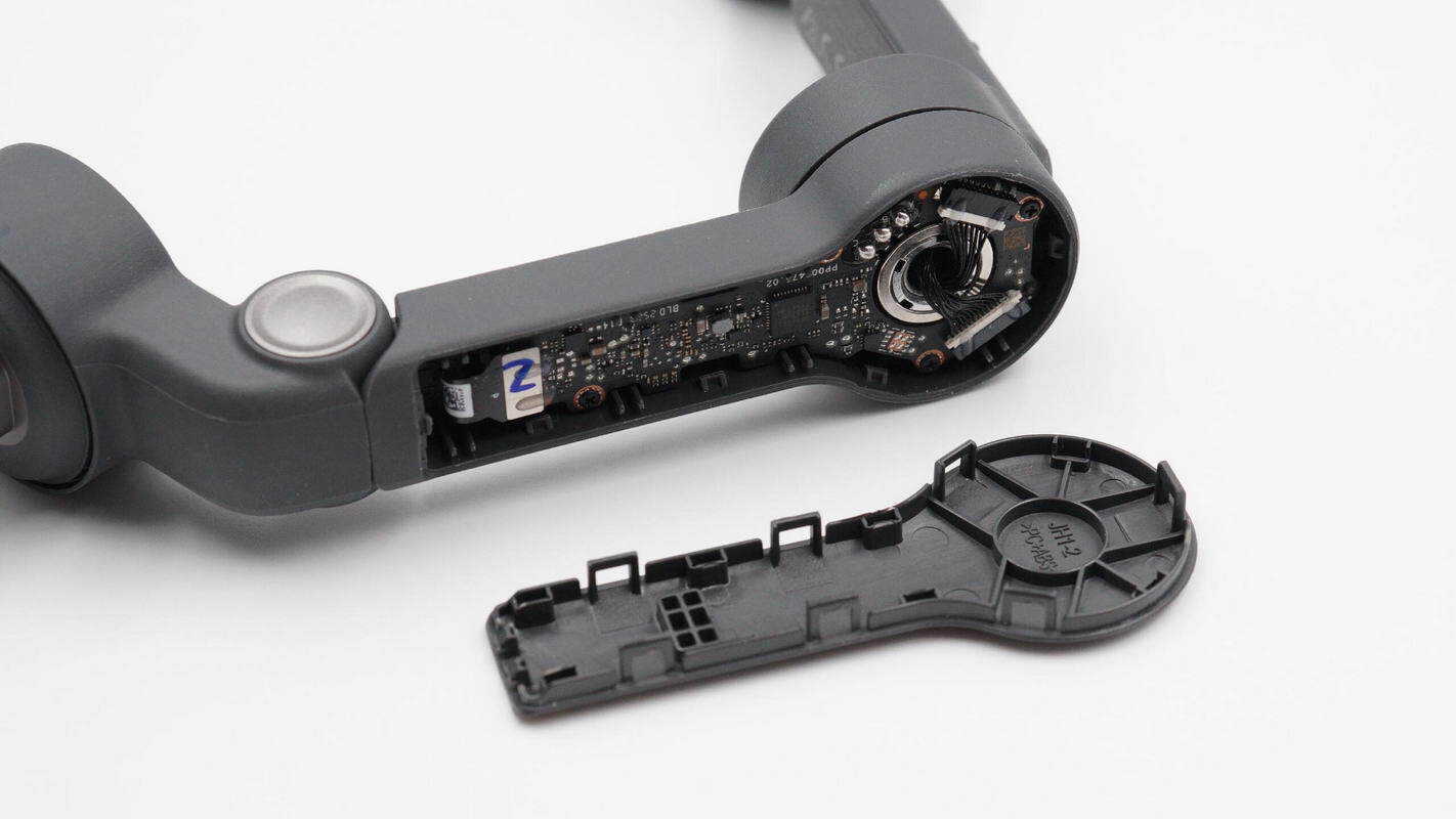
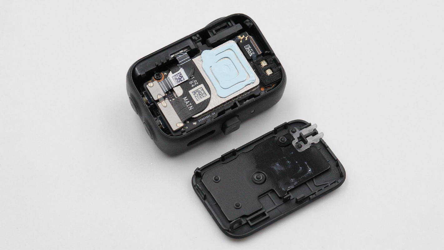
Unscrew the mounting screws of the extension rod cover plate.
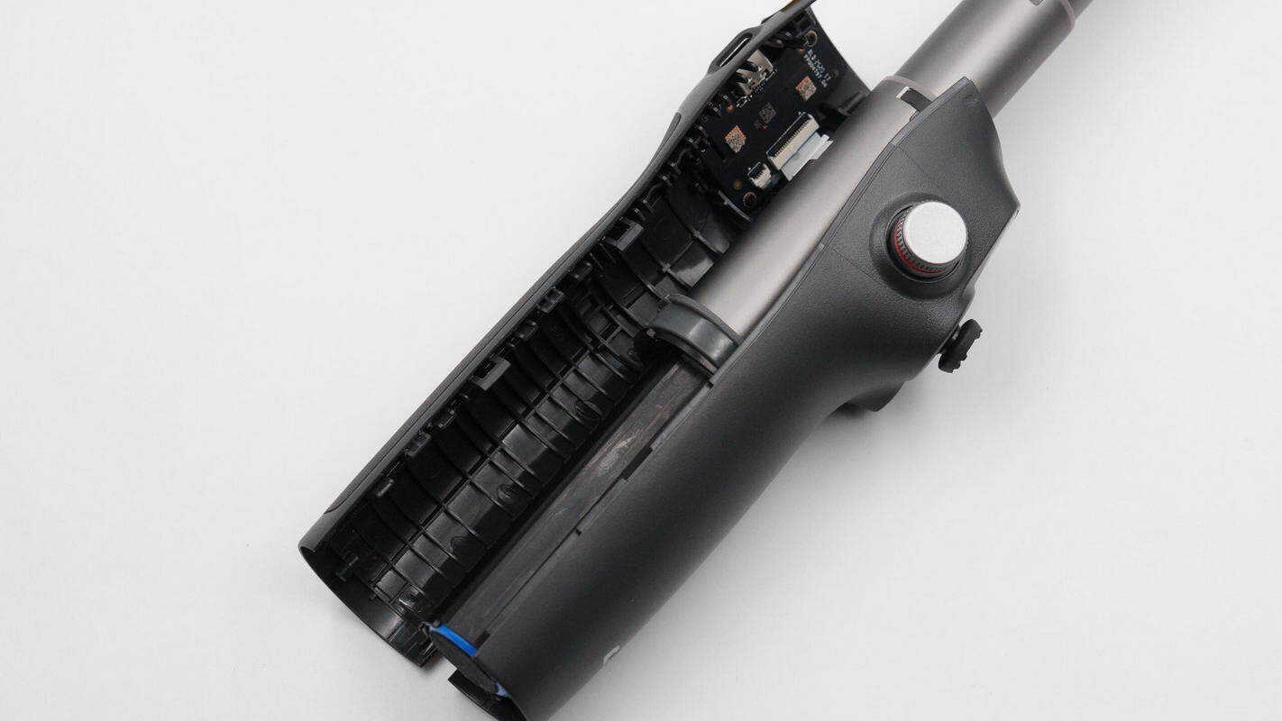
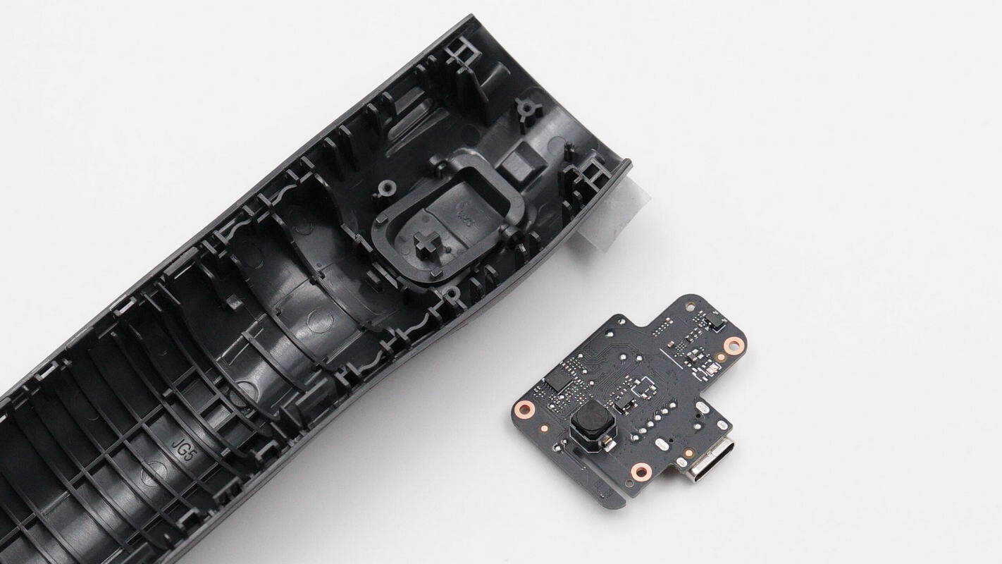
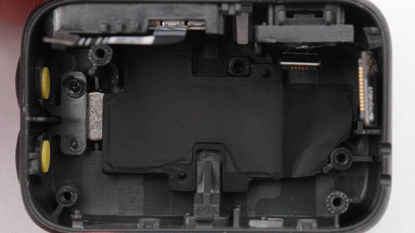
Open the handle along the case seam; the handle casing is secured with clips.
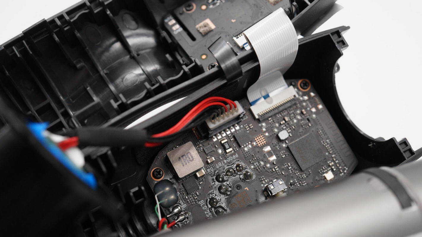
Inside the handle, there are two PCBA modules connected by a ribbon cable.
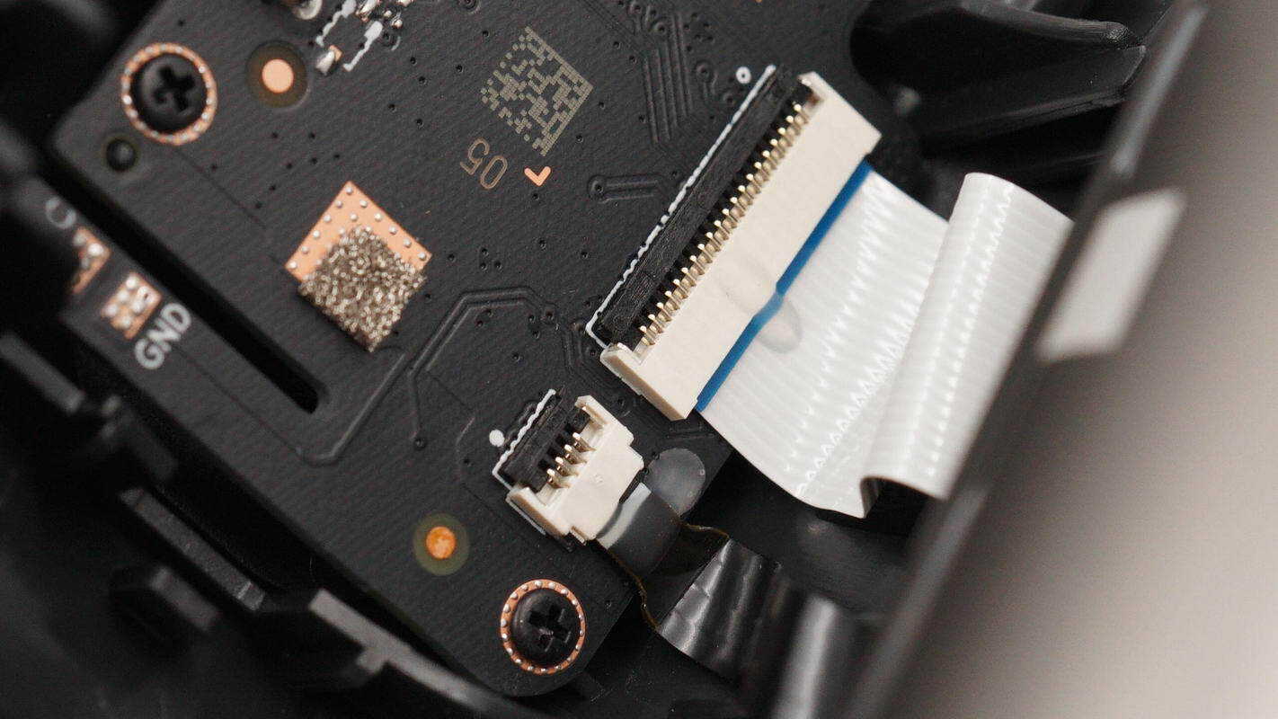
The connector is used to link the PCBA modules with the NFC coil.
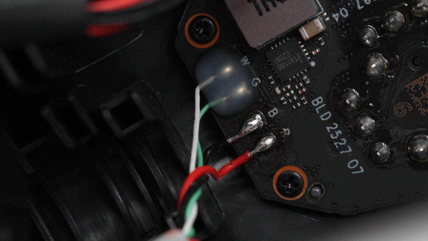
The extension rod is connected via soldered wires, with the solder joints reinforced using adhesive.

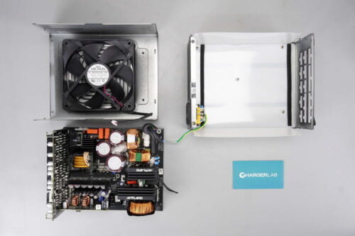
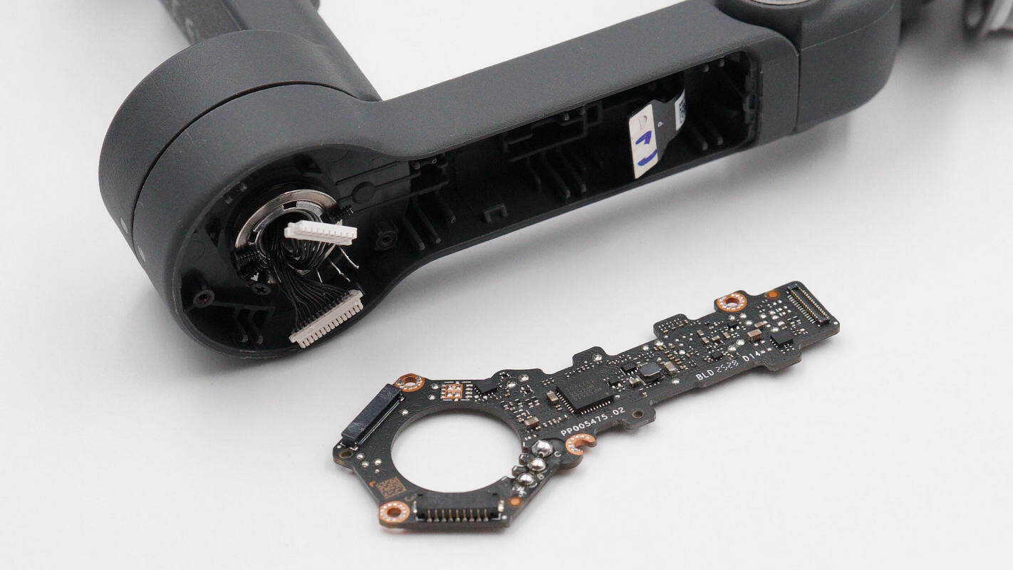
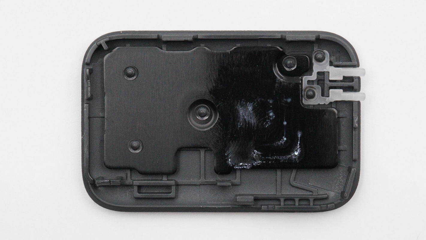
Disassemble the handle by opening the casing and removing the internal extension rod and battery pack.
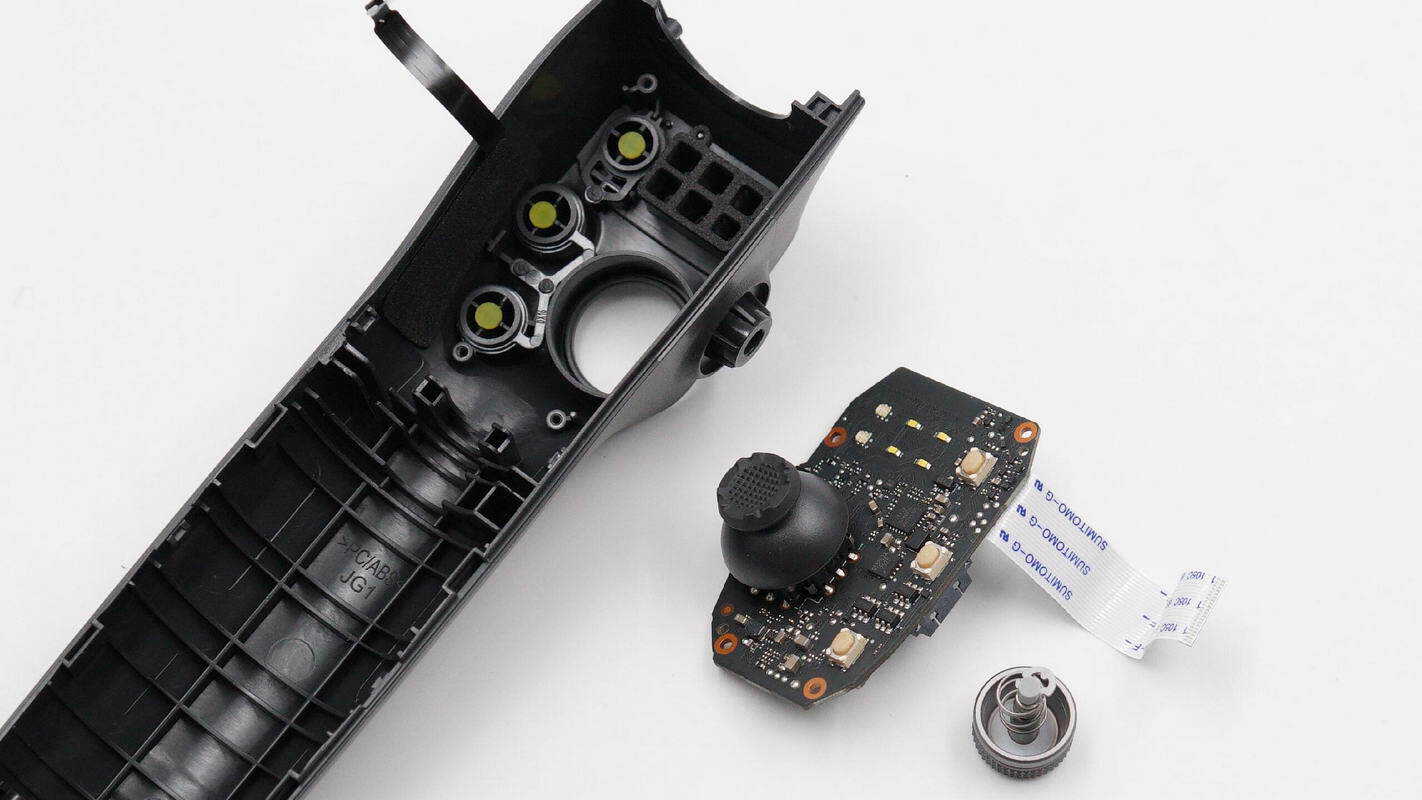
Unscrew the mounting screws, remove the control wheel retaining clip, and take out the internal PCBA module.
The head of the control wheel is equipped with a magnet.
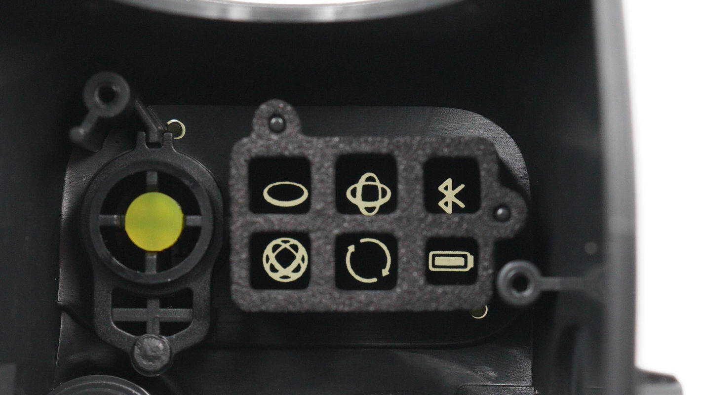
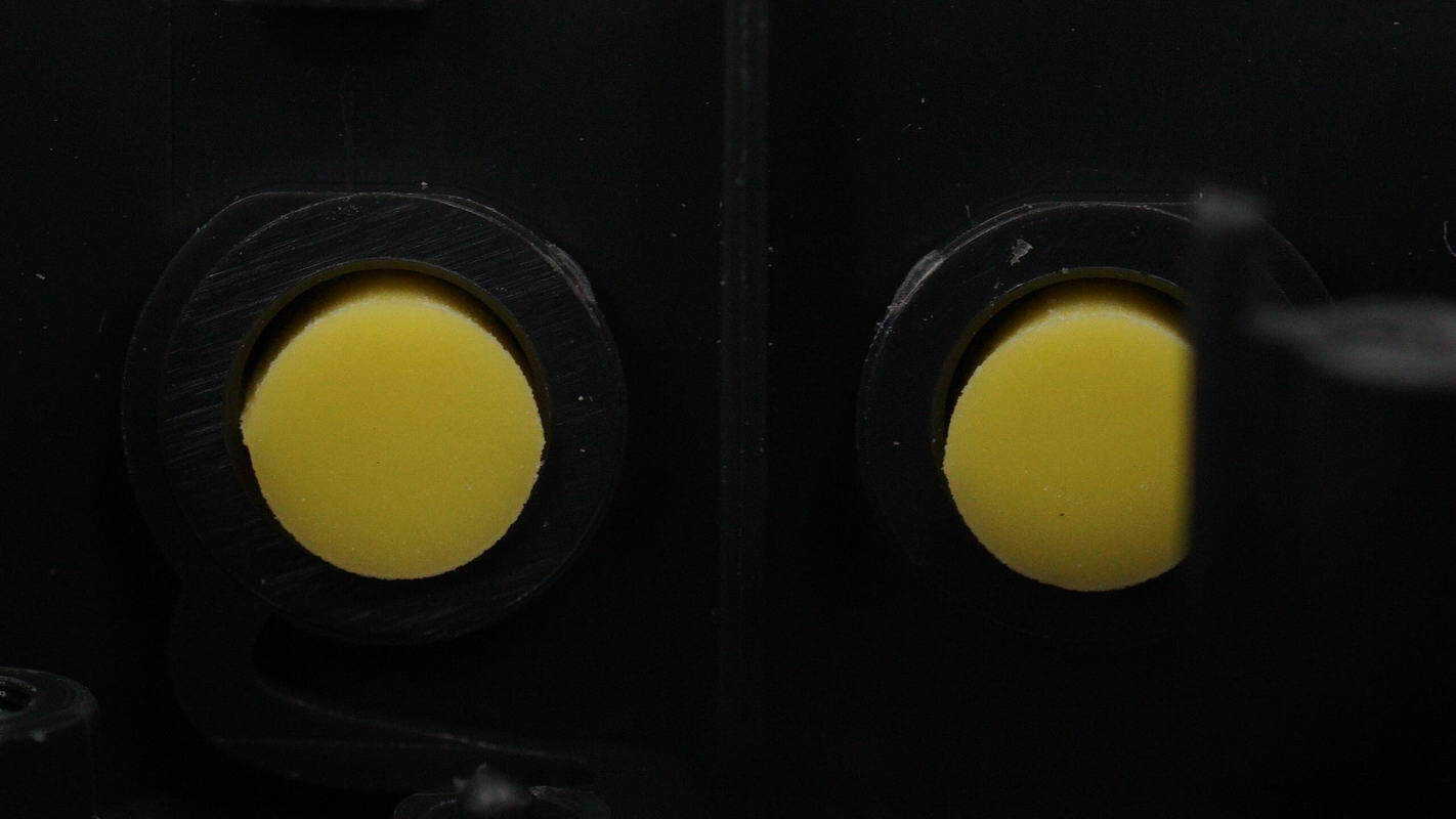
Close-up of the indicator light window inside the status display panel, equipped with foam for light shielding.

Rubber pads are installed inside the buttons to provide cushioning and enhance tactile feedback.
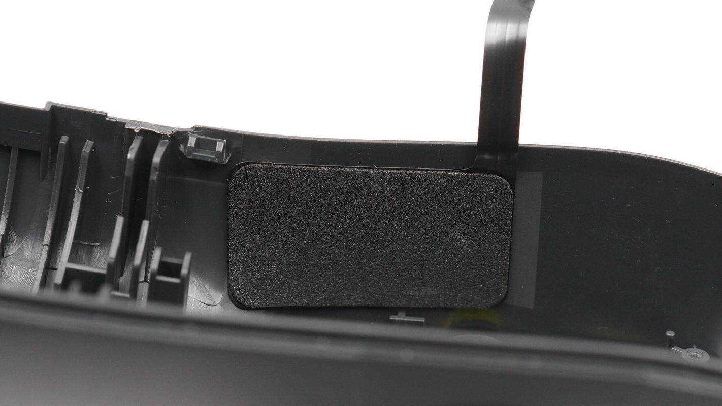
Close-up of the NFC coil patch inside the handle casing.
Unscrew the mounting screws and remove the small PCB for the trigger button.
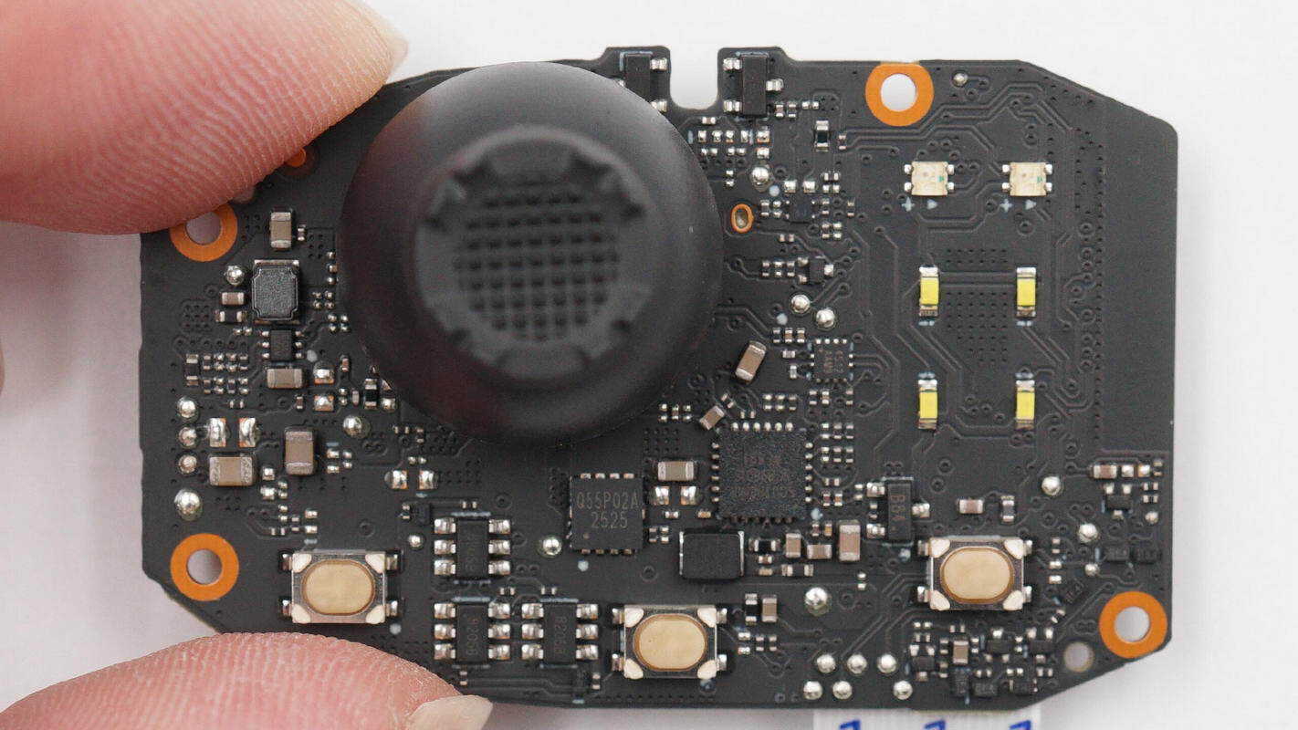
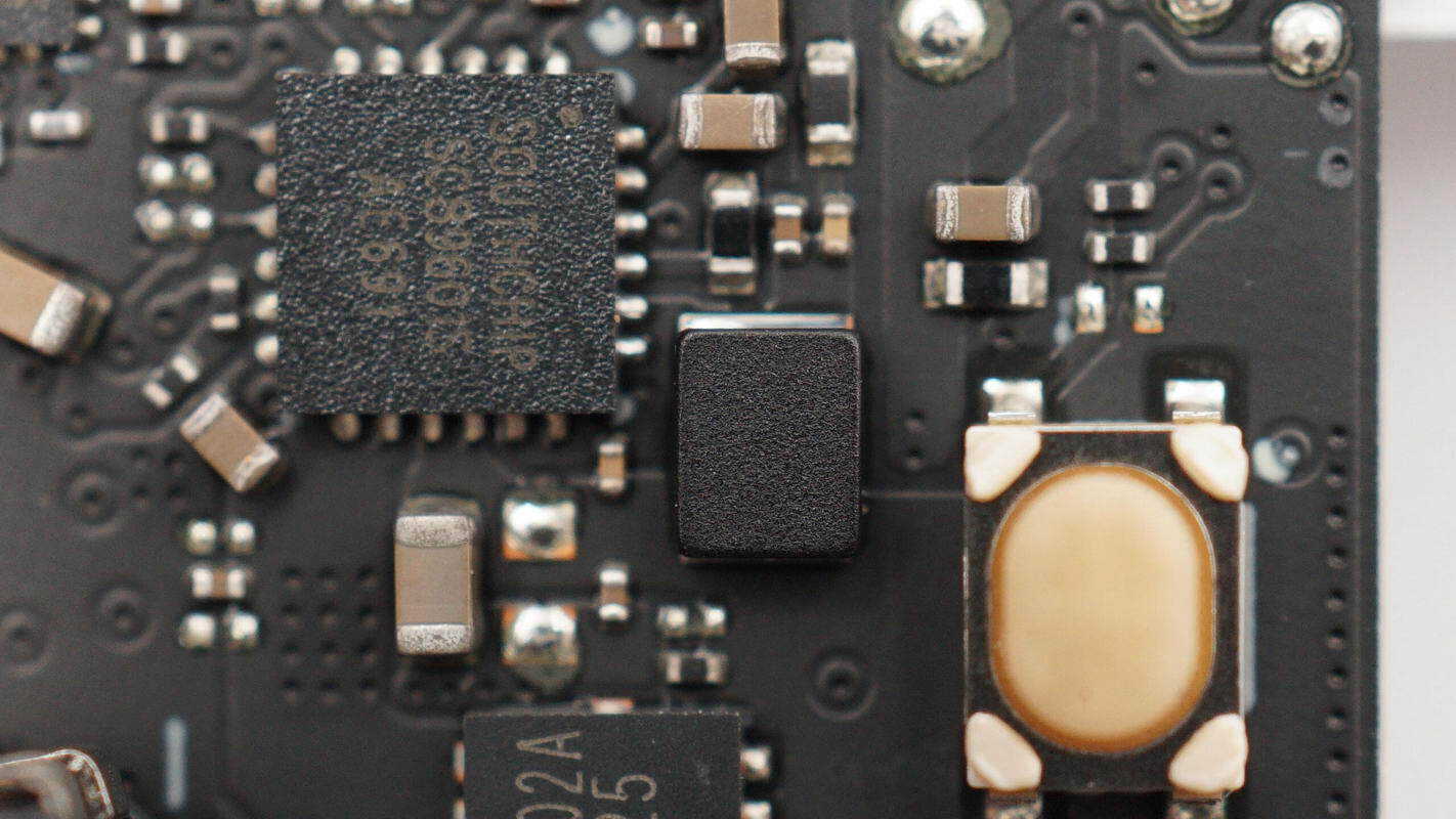
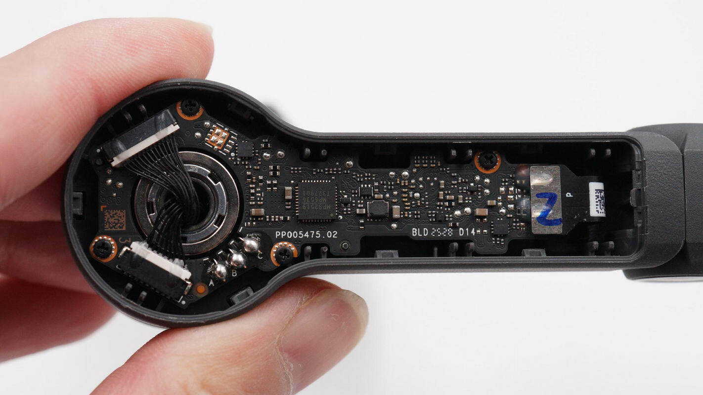
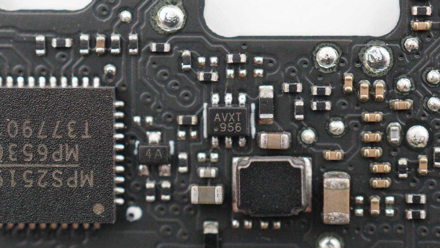
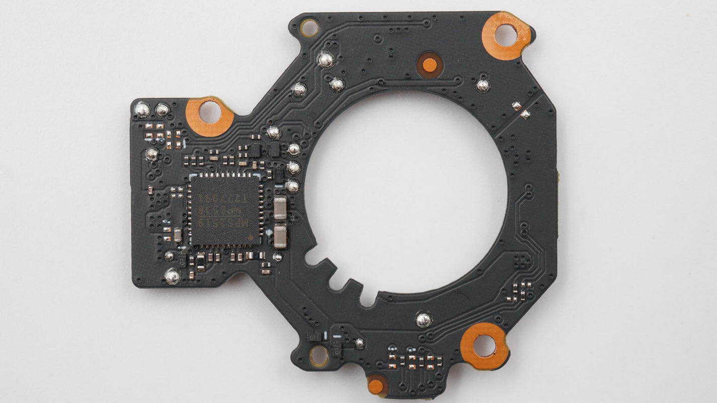
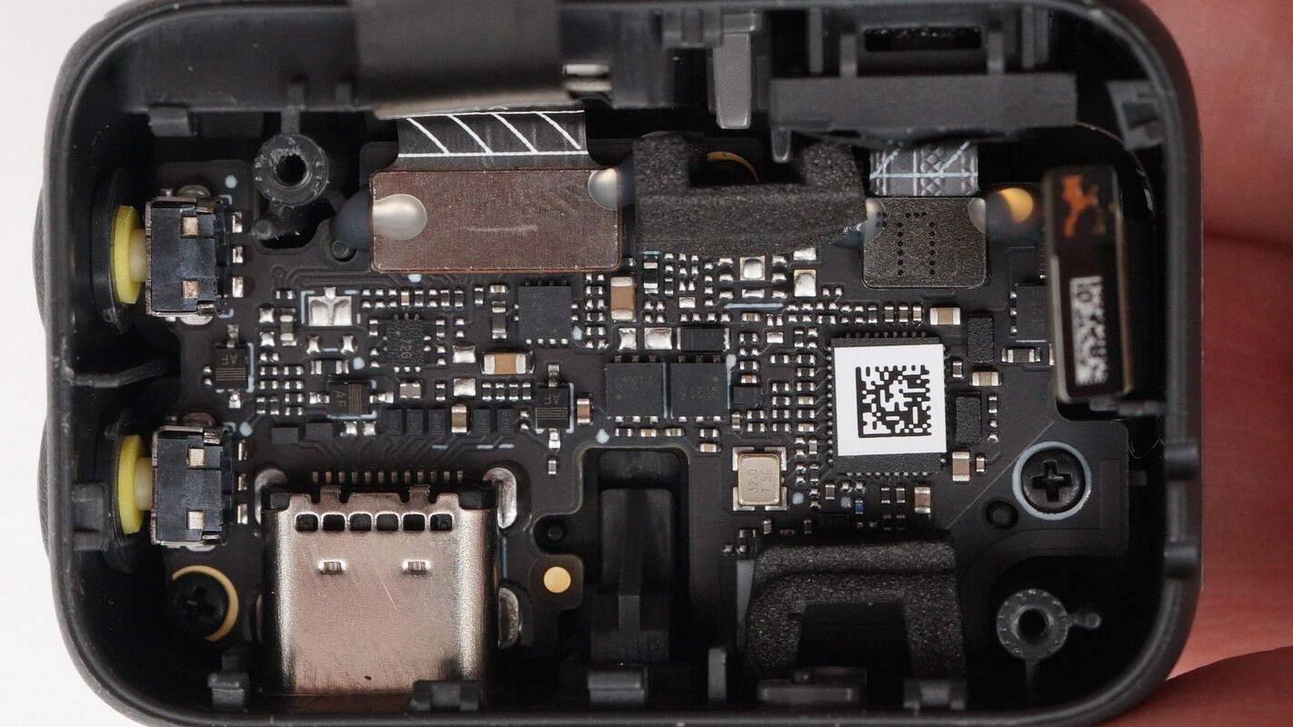
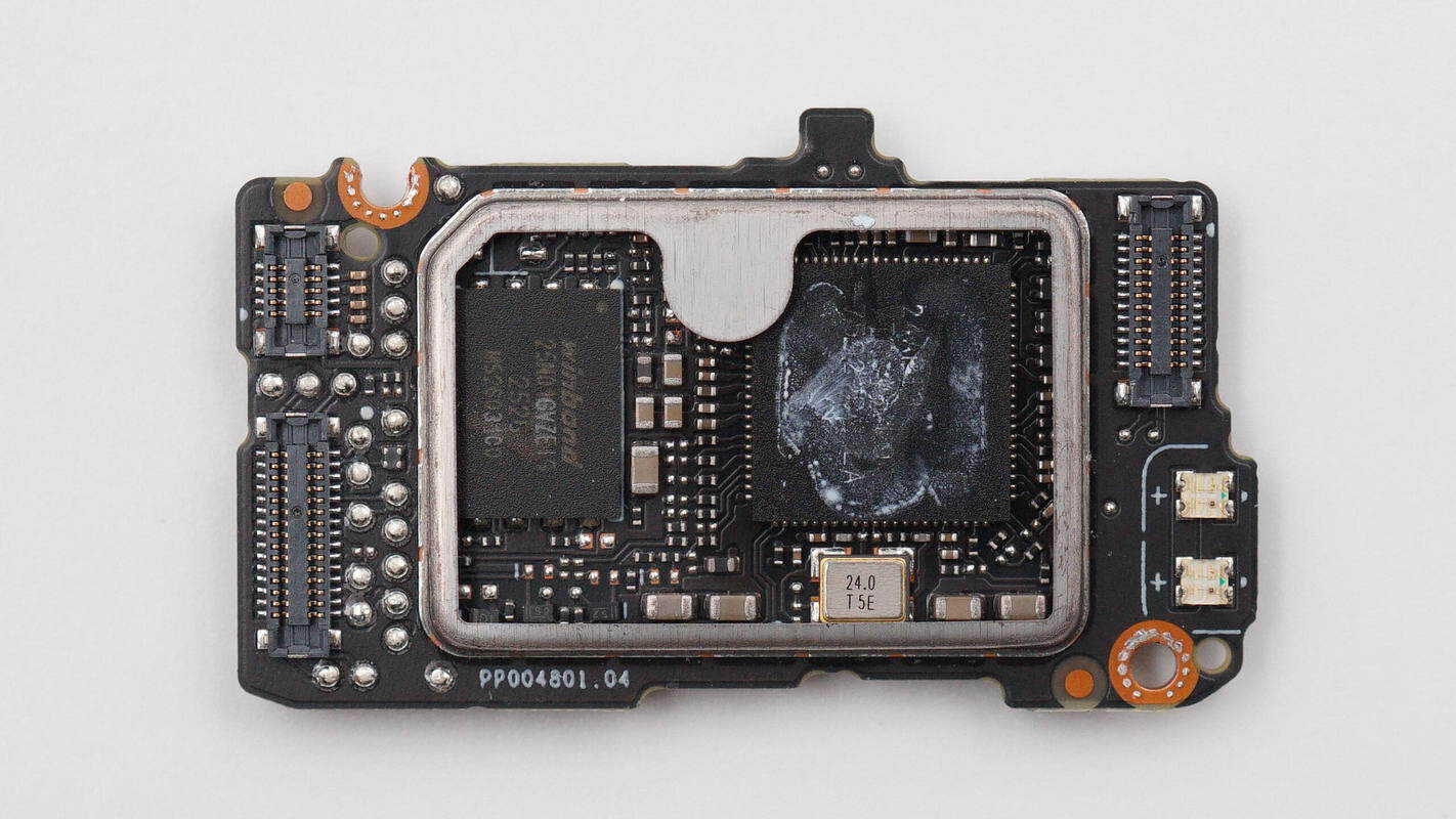
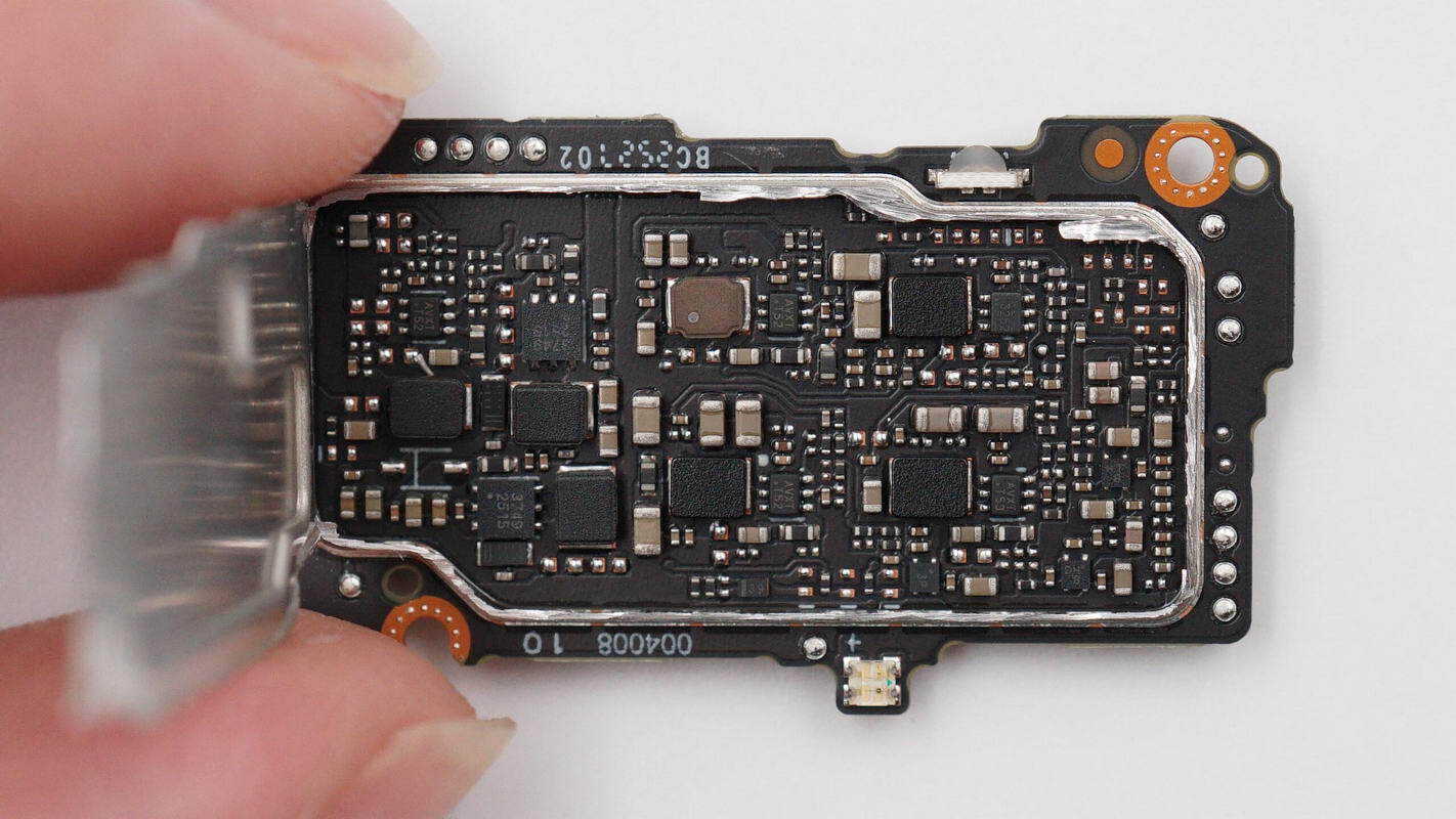
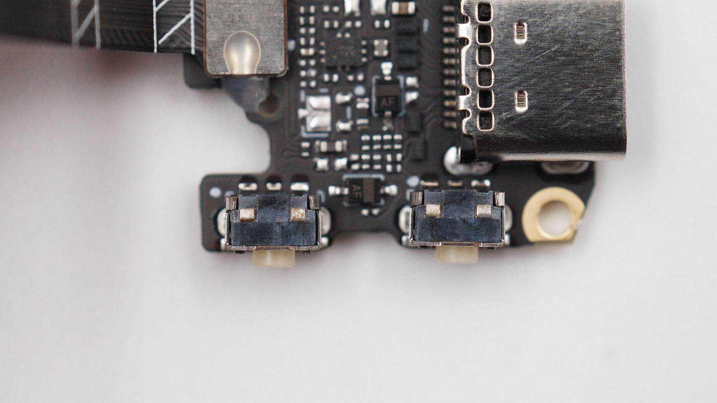
Overview of the front side of the PCBA module: the joystick is located at the top left, the charging chip at the bottom right, the LED indicator lights on the right, and three buttons at the bottom.
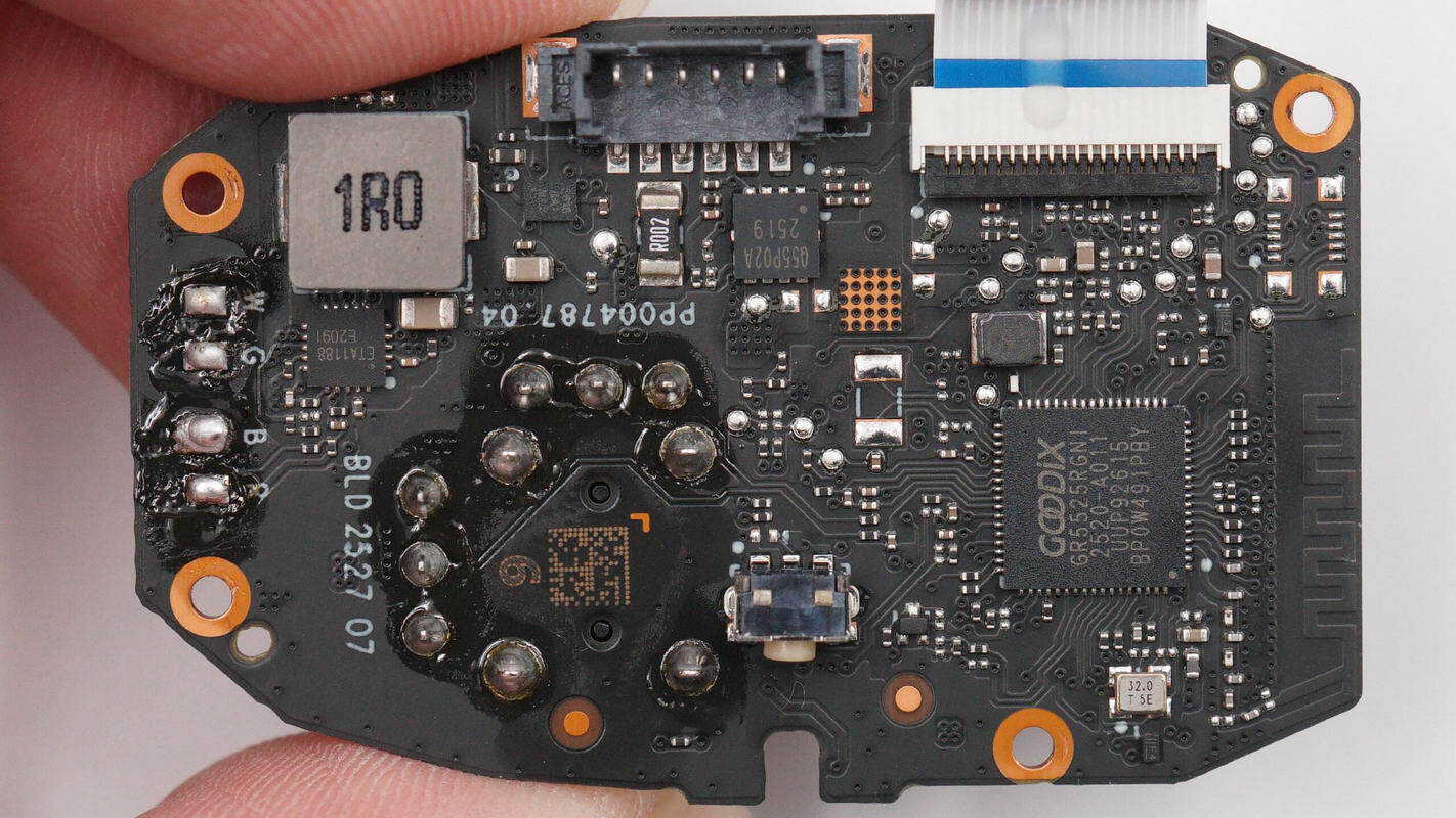
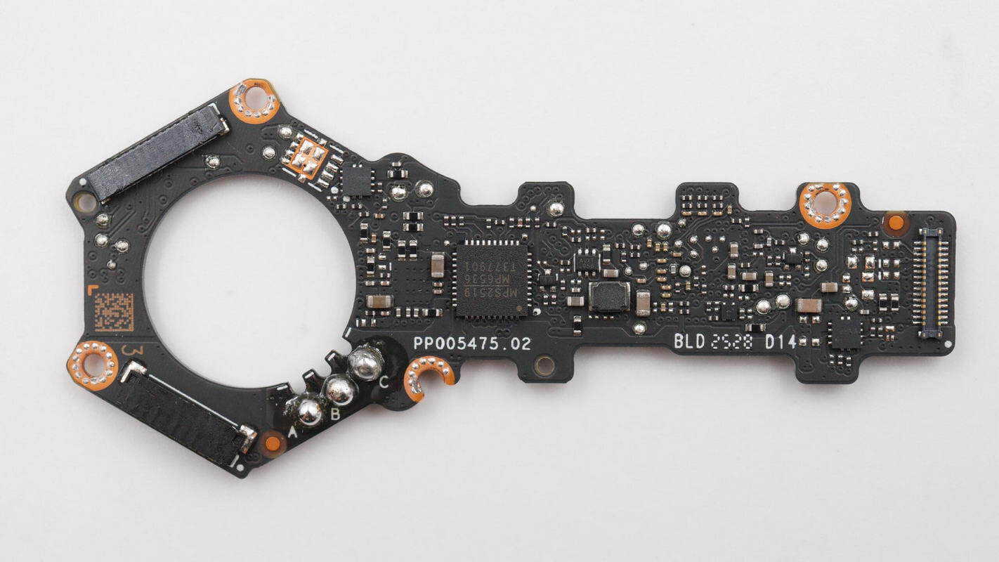
The back side features a boost inductor, a synchronous boost converter, a VBUS MOSFET, and the master control chip.
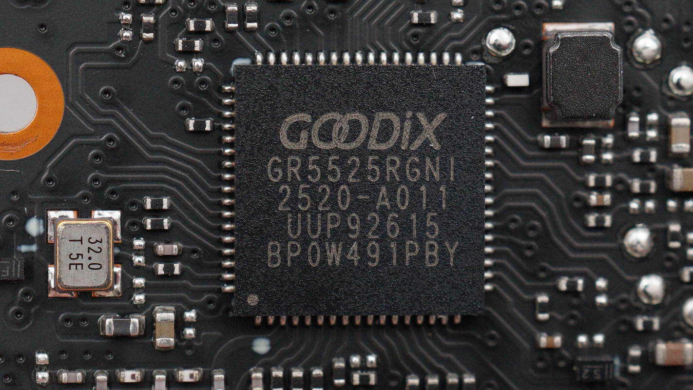
The Bluetooth SoC is from Goodix, model GR5525RGNI. The chip supports single-mode low-power Bluetooth 5.3 and integrates an ARM Cortex-M4F CPU with a 96 MHz main frequency. It has 1 MB of flash memory and 256 KB of RAM, and includes an integrated Bluetooth protocol stack and a 2.4 GHz RF transceiver. It supports I²C, UART, and QSPI interfaces, targeting IoT and wearable applications, and comes in a QFN68 package.

Close-up of the external 32 MHz crystal oscillator, with the printed Bluetooth antenna on the right.
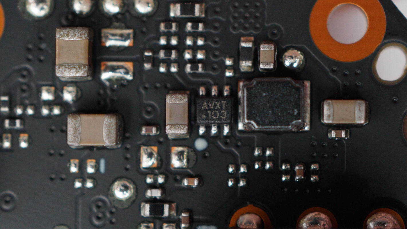
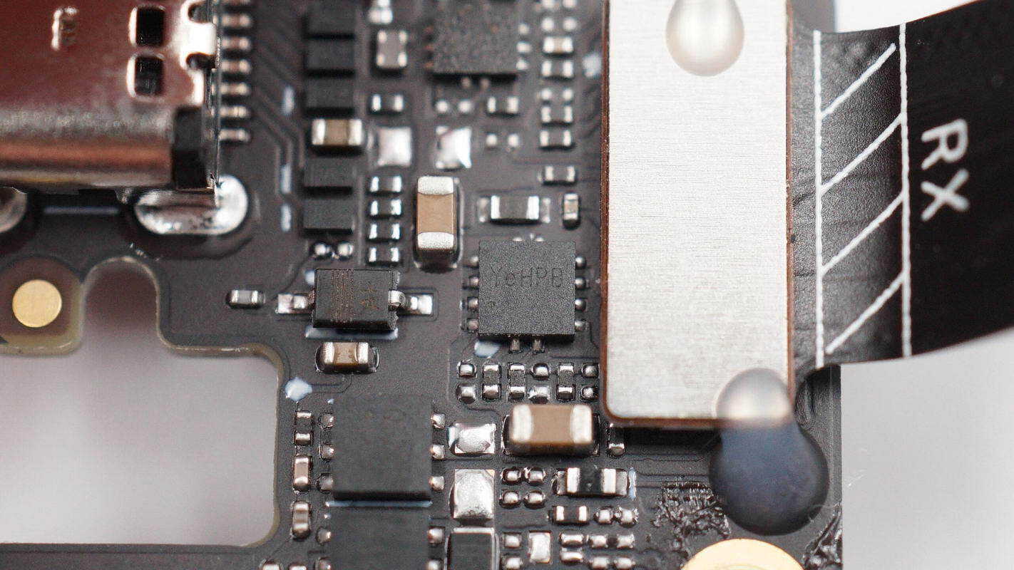
The synchronous buck chip is from MPS, marked with AVX, and comes in a SOT-563 package.
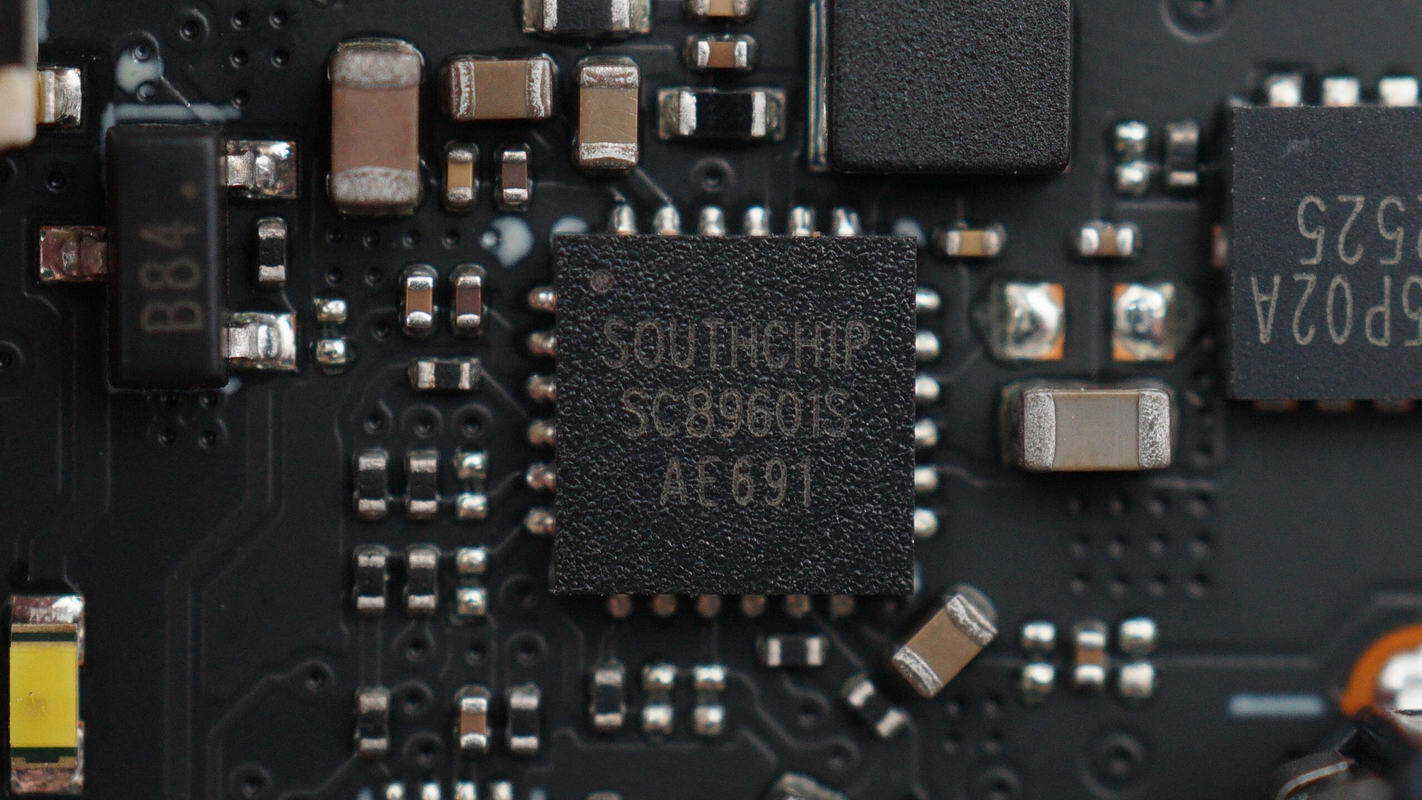
The battery charging chip is from SouthChip, model SC89601S. It is a high-efficiency synchronous 3 A buck charger designed for a single-cell lithium-ion battery, featuring NVDC power path management. It supports an input voltage of 3.9–13.5 V, a charging current up to 3 A, and a switching frequency of 1.5 MHz. The chip provides full battery management functions, including trickle charge, constant current charge, constant voltage charge, charge termination, automatic recharge, and charging status indication. It comes in a QFN 4×4 package.
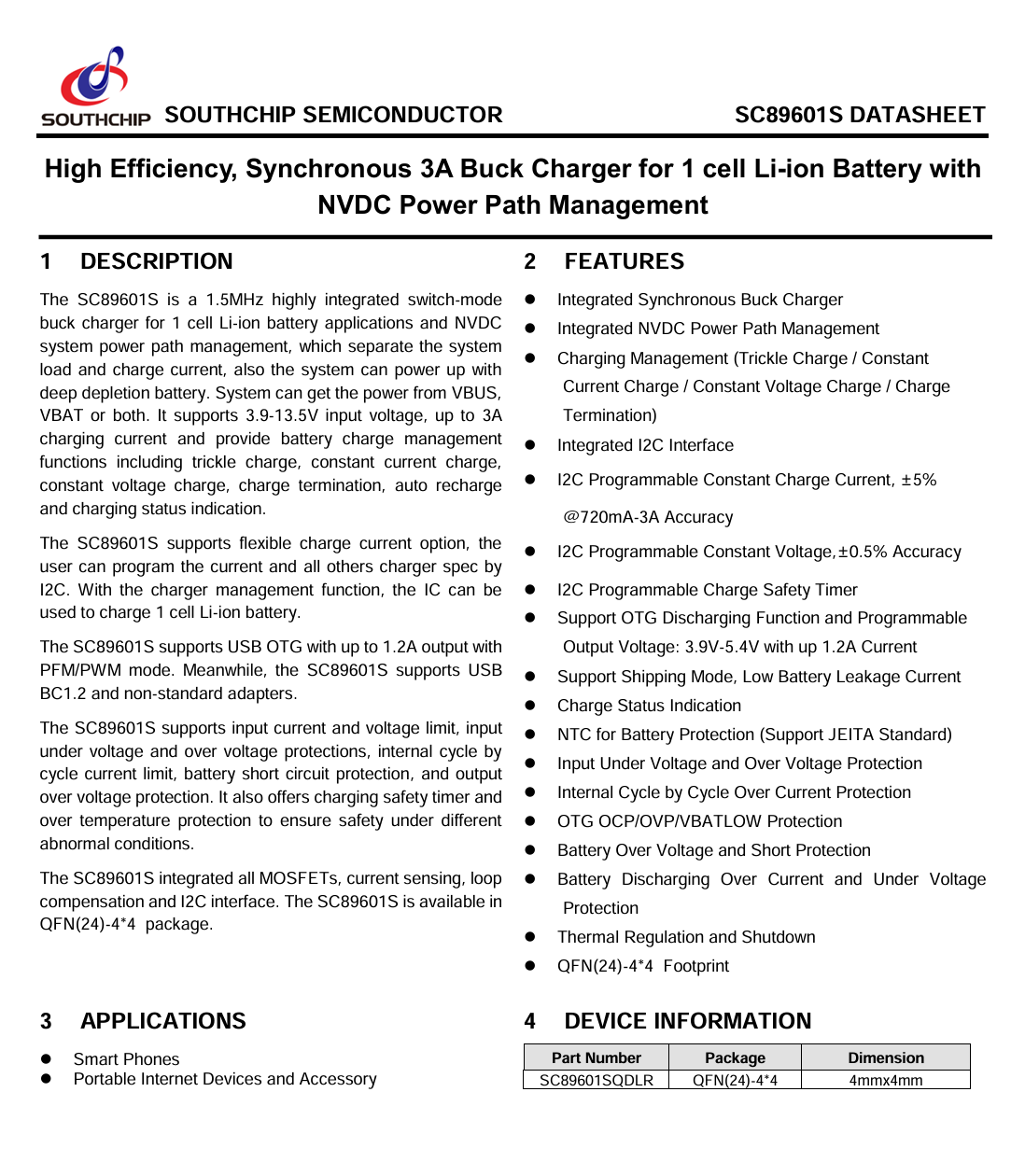
Here is the information about SouthChip SC89601S.
Close-up of the external SMD inductor connected to the chip.
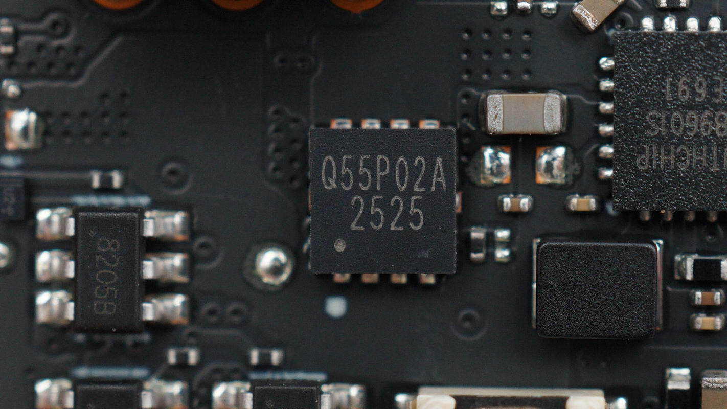
The MOSFET used for power control is from YJ, model YJQ55P02A. It is a PMOS with a voltage rating of –20 V and an on-resistance of 6.5 mΩ. It comes in a DFN 3.3×3.3 package and is suitable for high-current applications, including load switching, hard switching, high-frequency circuits, and UPS systems.

Another MOSFET with the same model is also used.
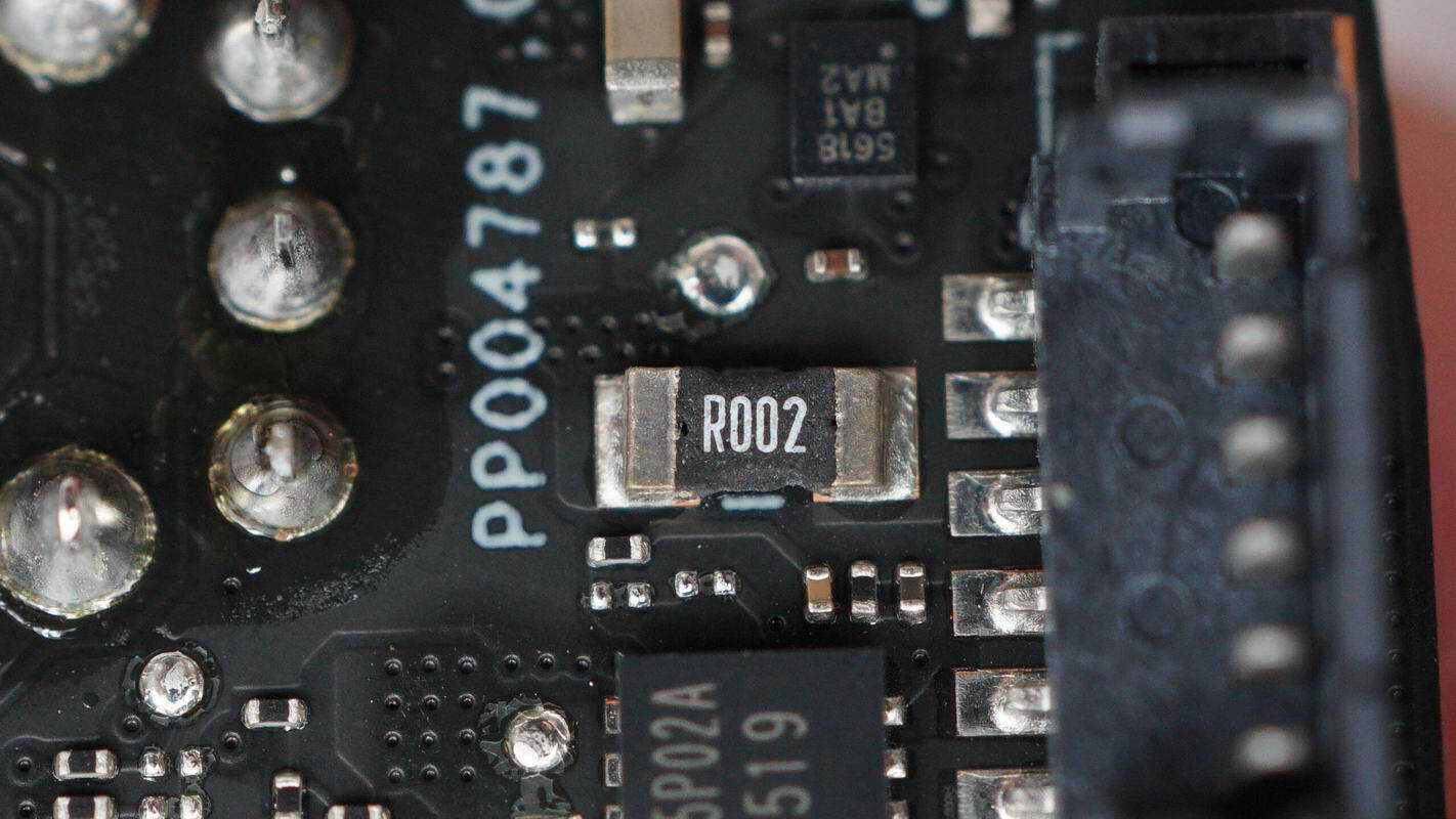
A 2 mΩ resistor is used for battery current sensing.
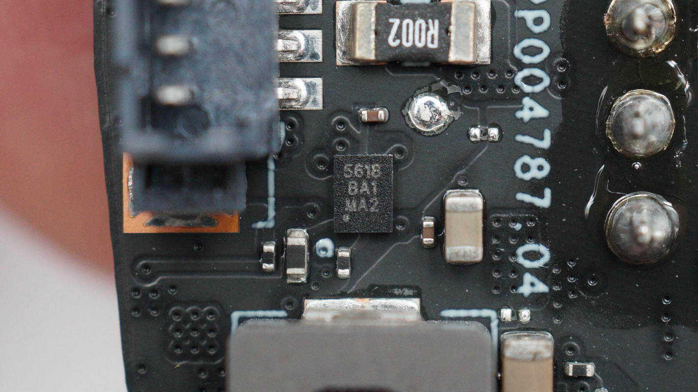
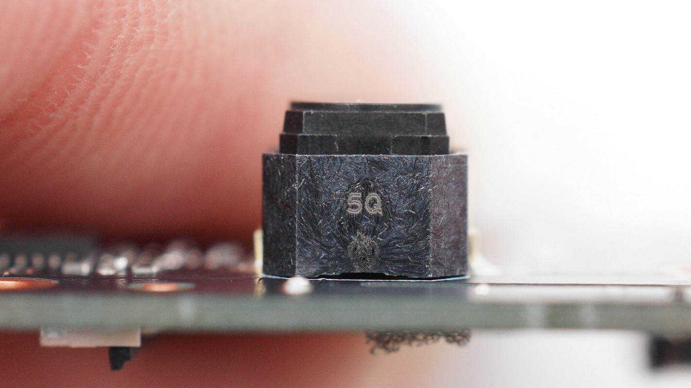
Close-up of a chip marked with 5618.
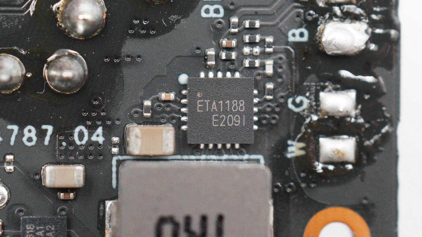
The synchronous boost chip is from ETA, model ETA1188. It is a synchronous boost converter with an internal MOSFET. The chip supports an input voltage of 2.7–12 V and an output voltage of 3.6–12 V. It has a built-in 20 mΩ NMOS for output shutdown. The chip features programmable overcurrent protection, and the output voltage can be adjusted via I²C or feedback. It comes in an FCQFN 3×3-20 package.
Here is the information about ETA ETA1188.
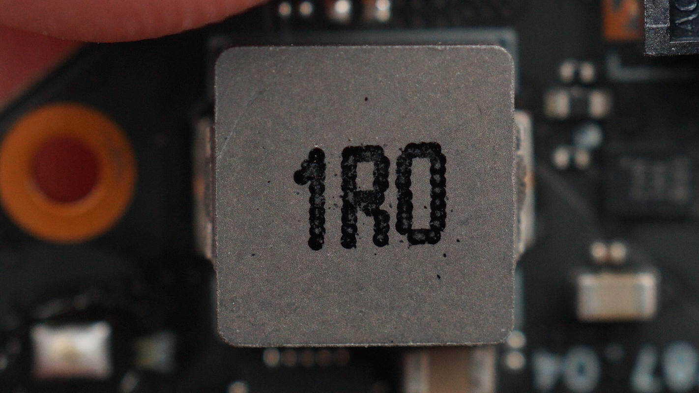
Close-up of the 1 μH alloy inductor.
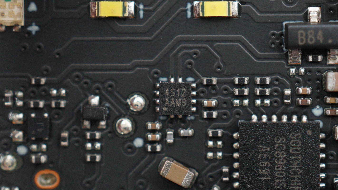
Close-up of a chip marked with 4S12AAM9.
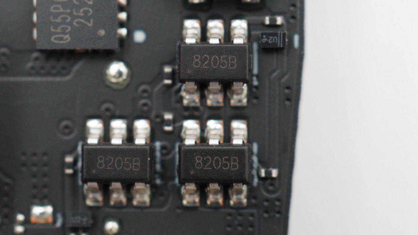
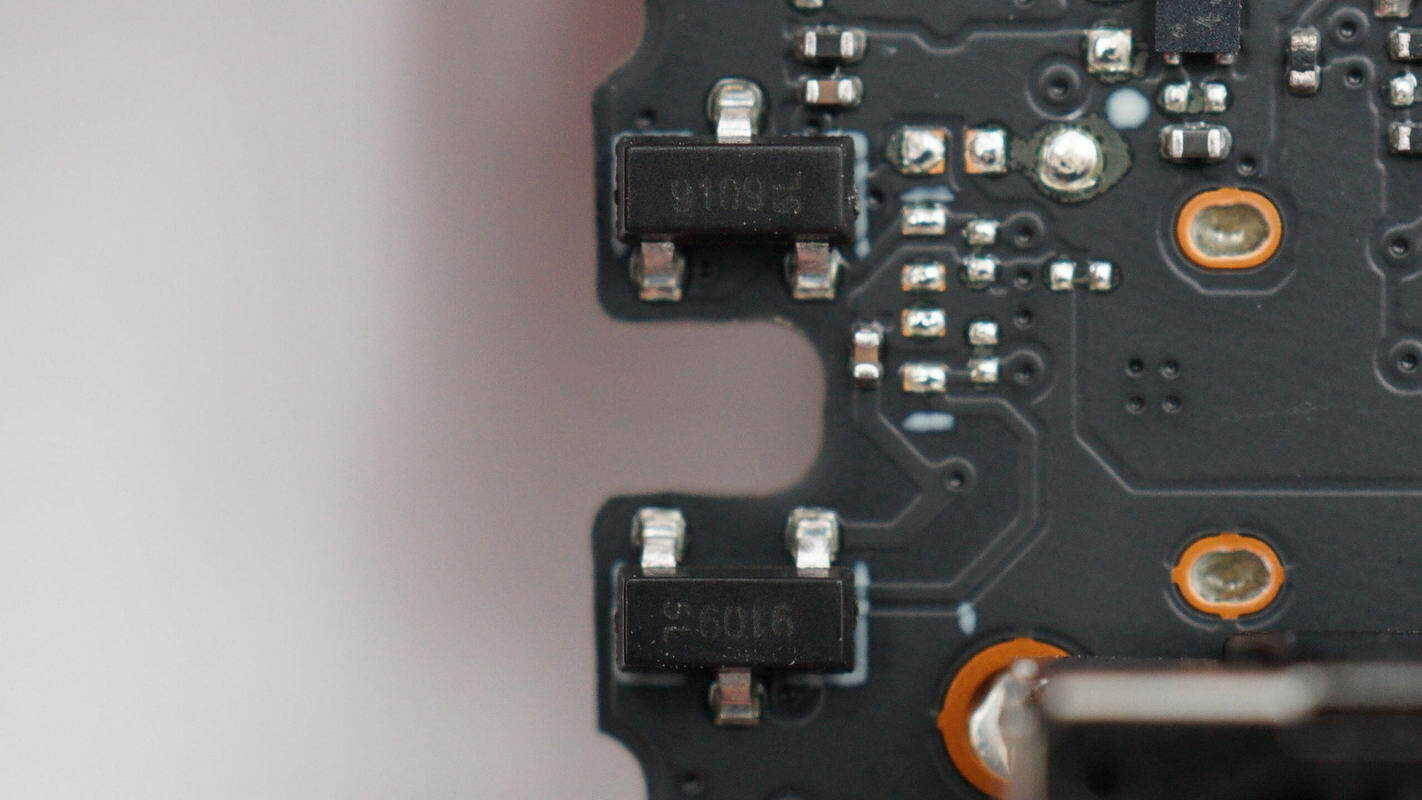
Three 8205B MOSFETs are used for power control.

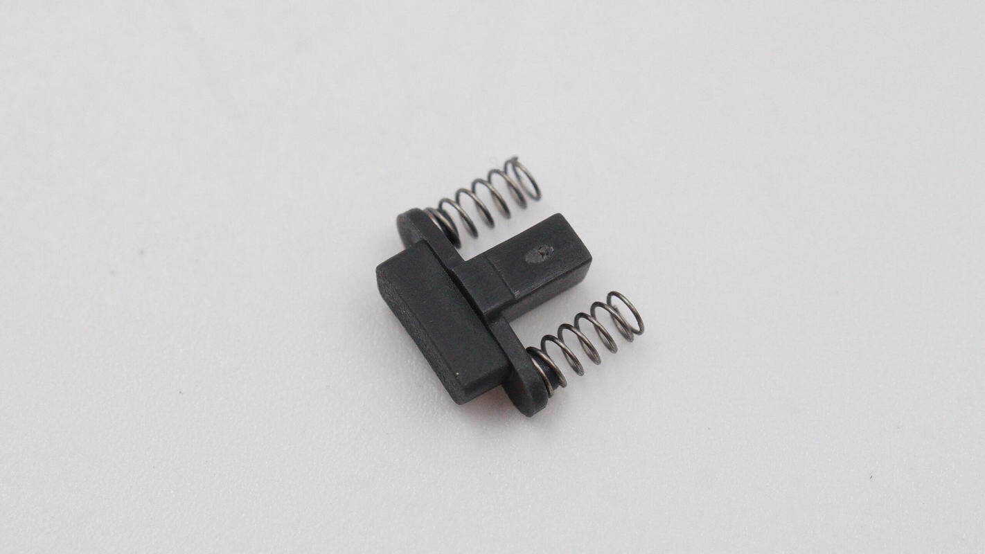
Remove the joystick cap; potentiometers are located on both sides of the joystick mechanism.
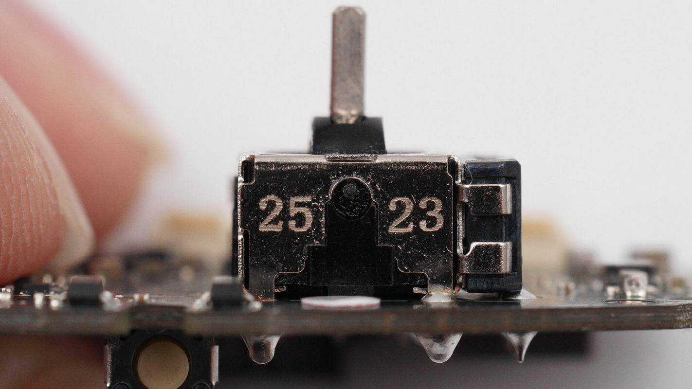
The joystick mechanism is secured through-hole soldered to the PCB.
The Hall element is from MagnTek, model MT9109. It is a linear Hall position sensing chip, supporting a 3–5.5 V operating voltage, and comes in an SOT-23 package.
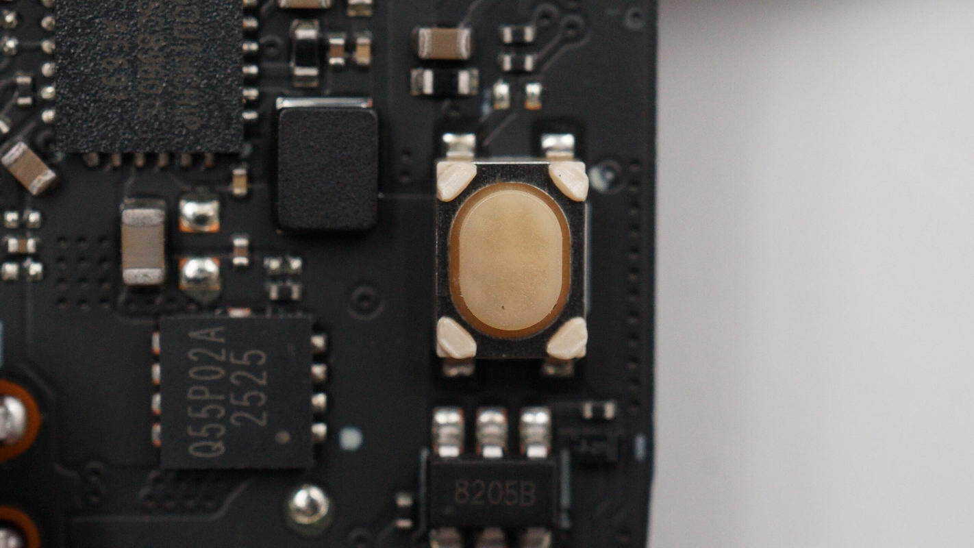
The function buttons are mounted using surface-mount soldering.
Close-up of the LED indicators on the status display panel.
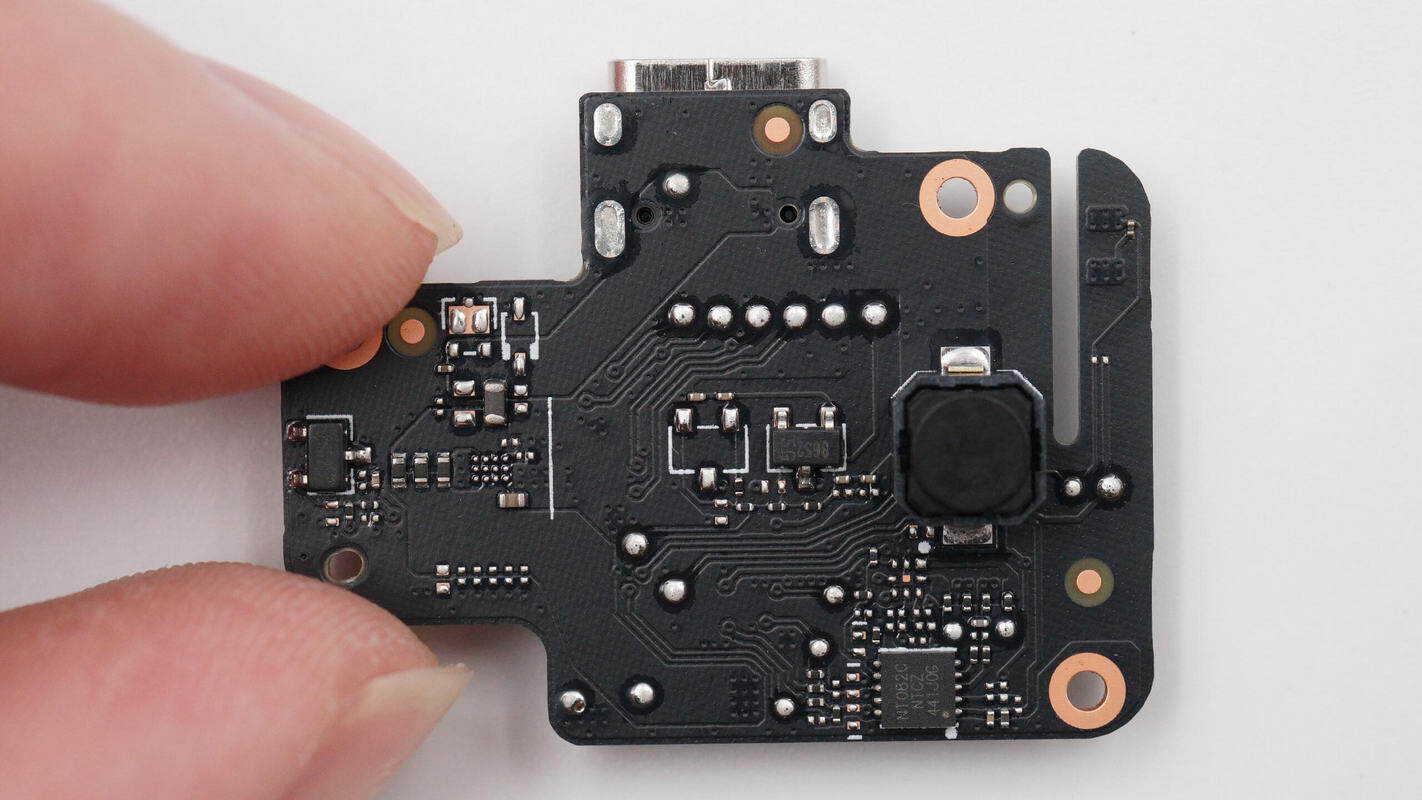
The trigger button PCB has magnetic switch position detection chips on the left and center, the trigger button on the right, and an NFC chip at the bottom.
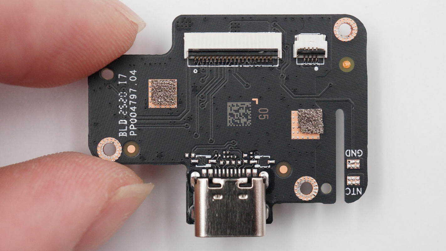
The back side features a USB-C socket and a connector.
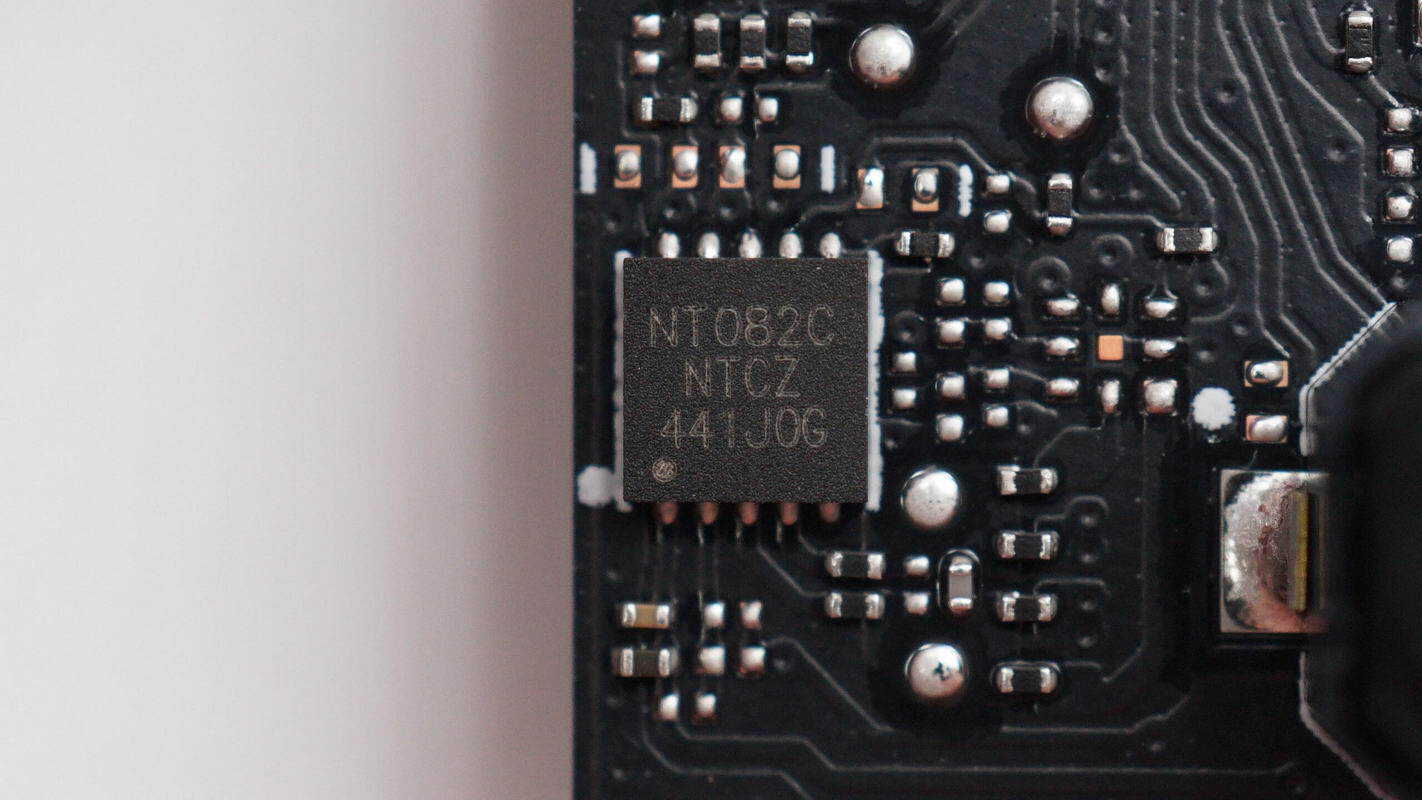
The NFC chip is from FUDAN, model FM11NT082C. It is an NFC dual-interface tag and transceiver chip, supporting the ISO/IEC14443-A communication protocol and a 2.2–5 V operating voltage range. It features built-in EEPROM and FIFO and comes in a TDFN10 package.
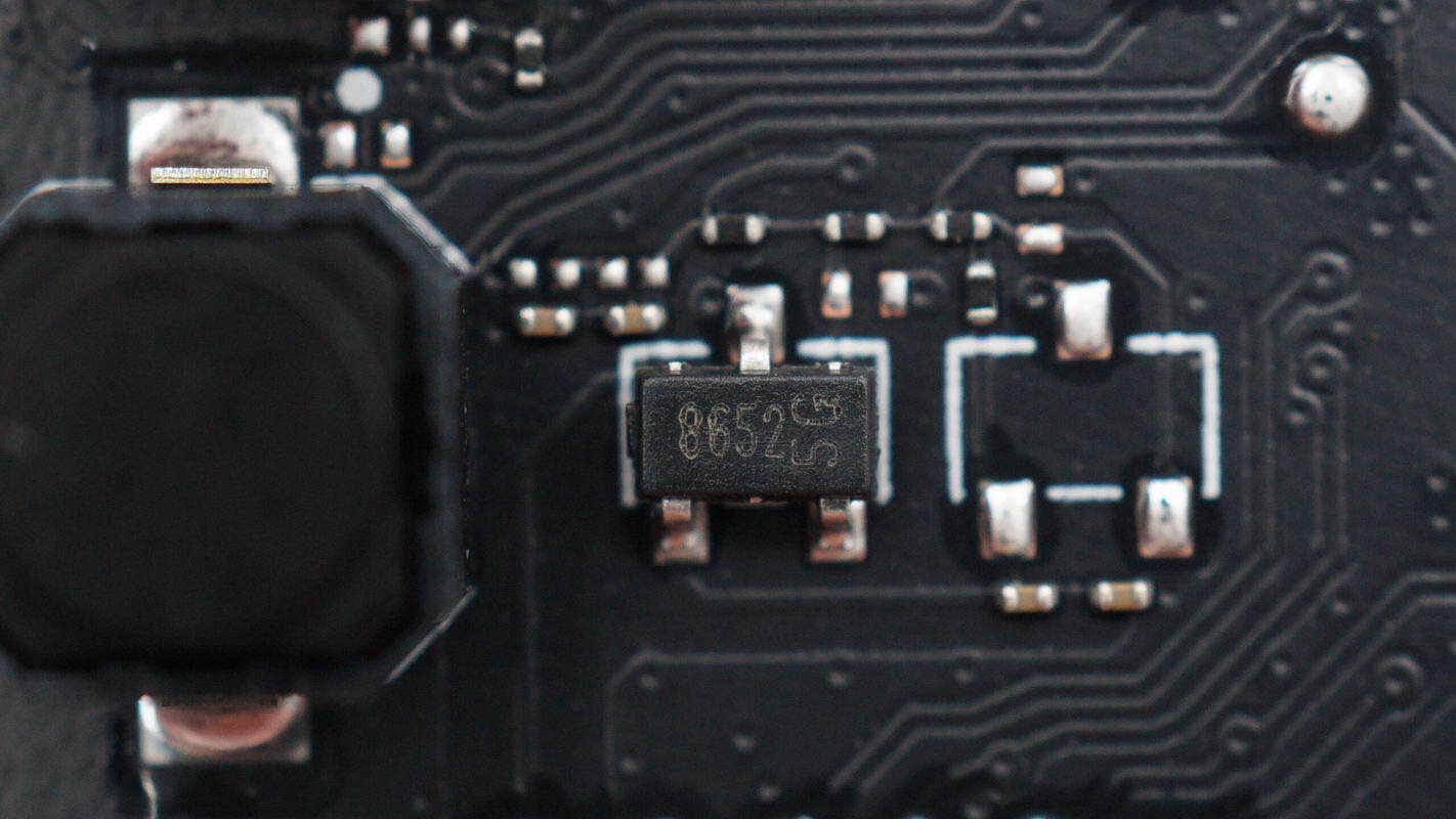
The magnetic switch position detection chip is from MagnTek, model MT8652. It uses CMOS technology, supports a 2–5.5 V operating voltage range, is automotive-grade certified, and comes in an SOT-23 package.
The trigger button is mounted using surface-mount soldering.
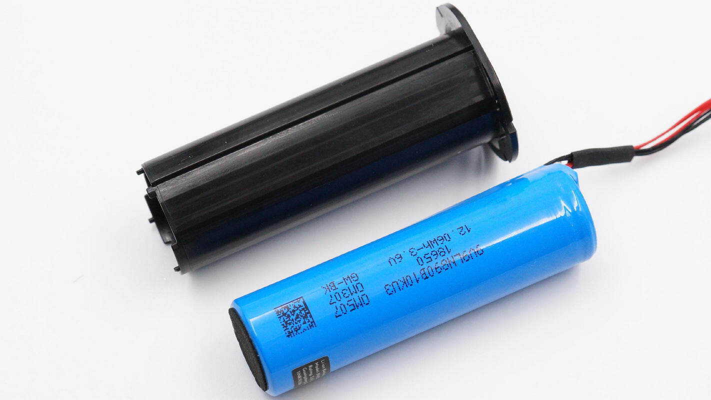
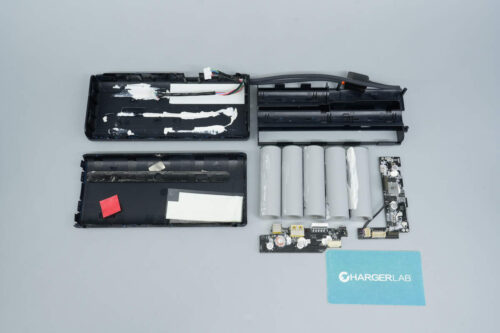
Remove the battery from the casing.
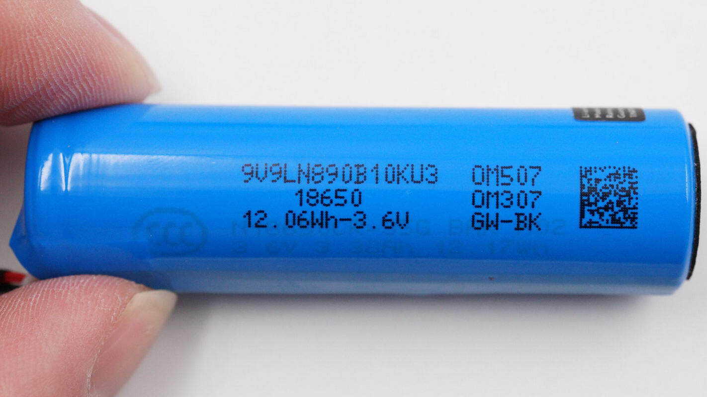
The battery is wrapped in a blue protective film and has an energy capacity of 120.6 Wh at 3.6 V.
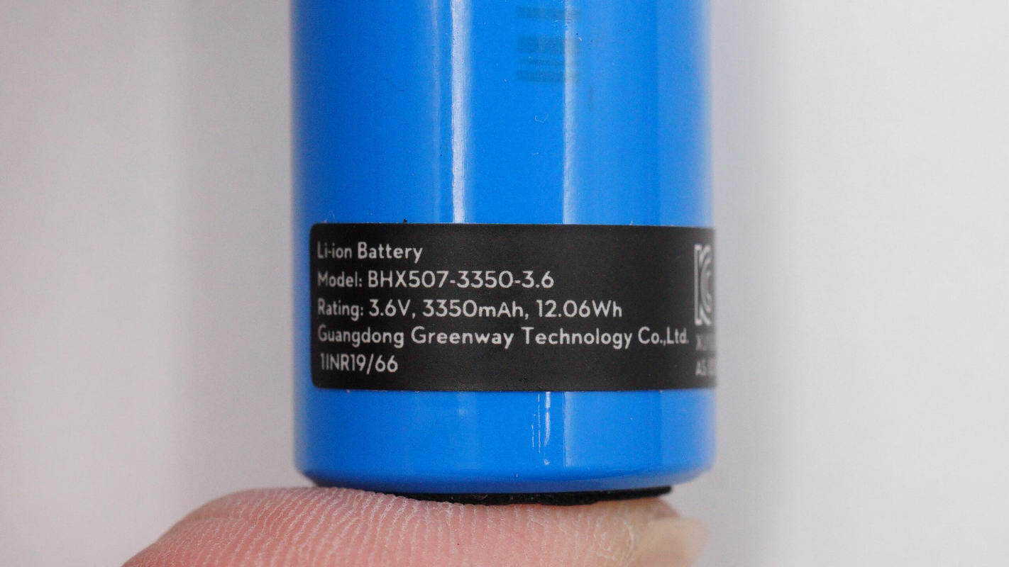
Lithium-ion battery
Model: BHX507-3350-3.6
Rated capacity: 3.6 V, 3350 mAh, 120.6 Wh

After removing the blue battery wrap, purple 18650 cells are visible inside.
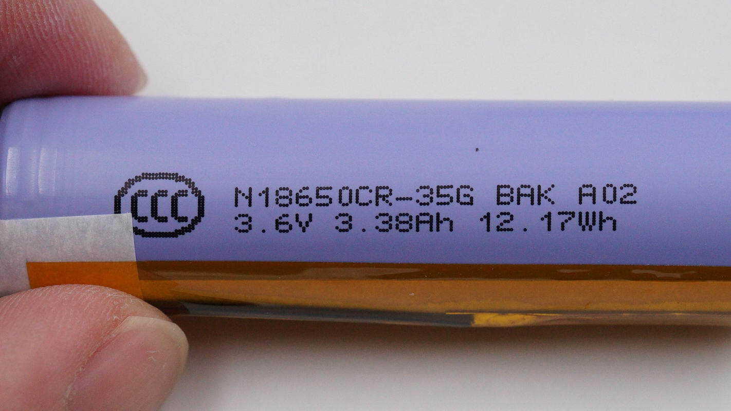
The battery is supplied by BAK, model N18650CR-35G, with a nominal voltage of 3.6 V, a nominal capacity of 3.38 Ah, and a nominal energy of 12.17 Wh.
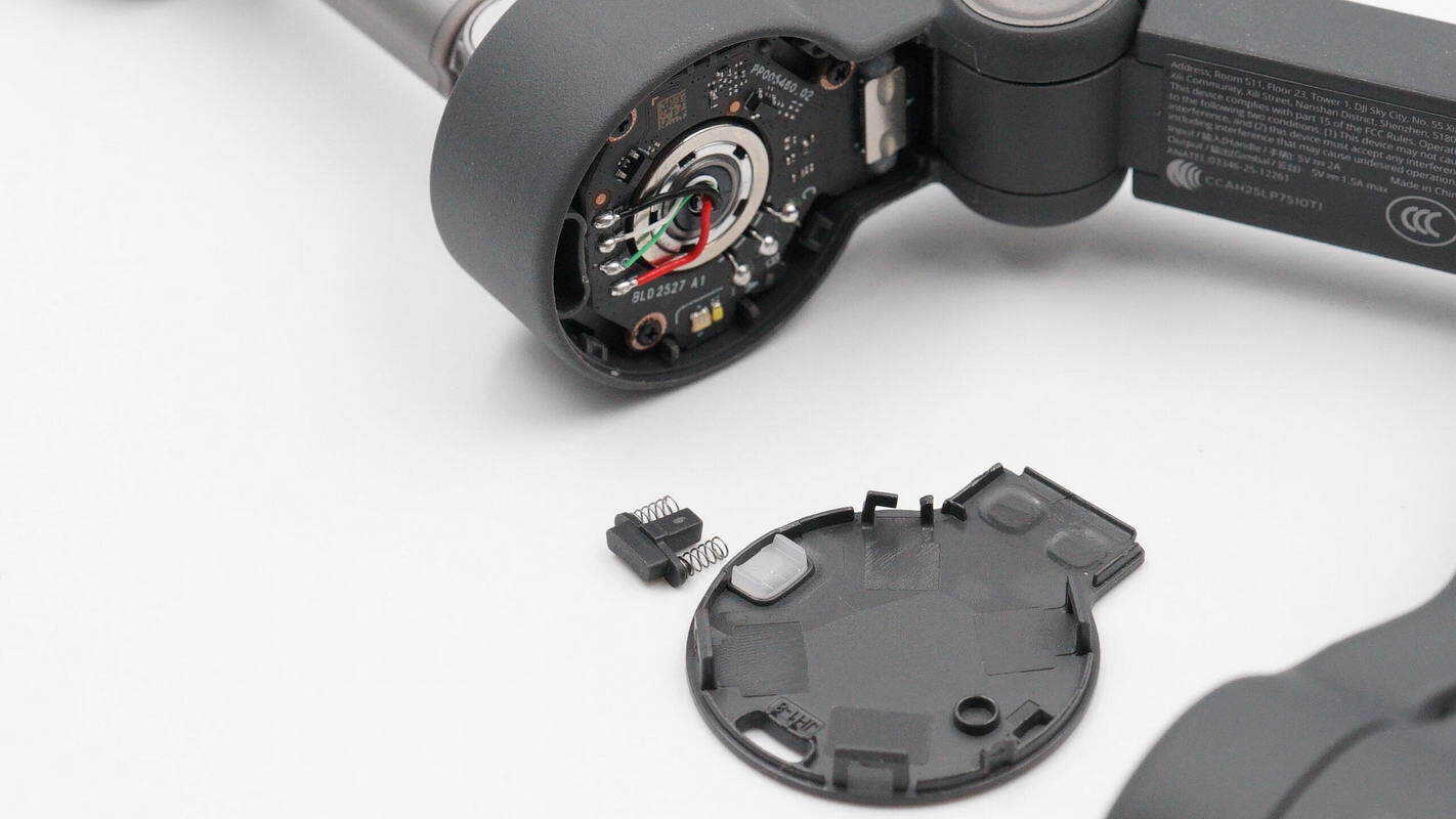
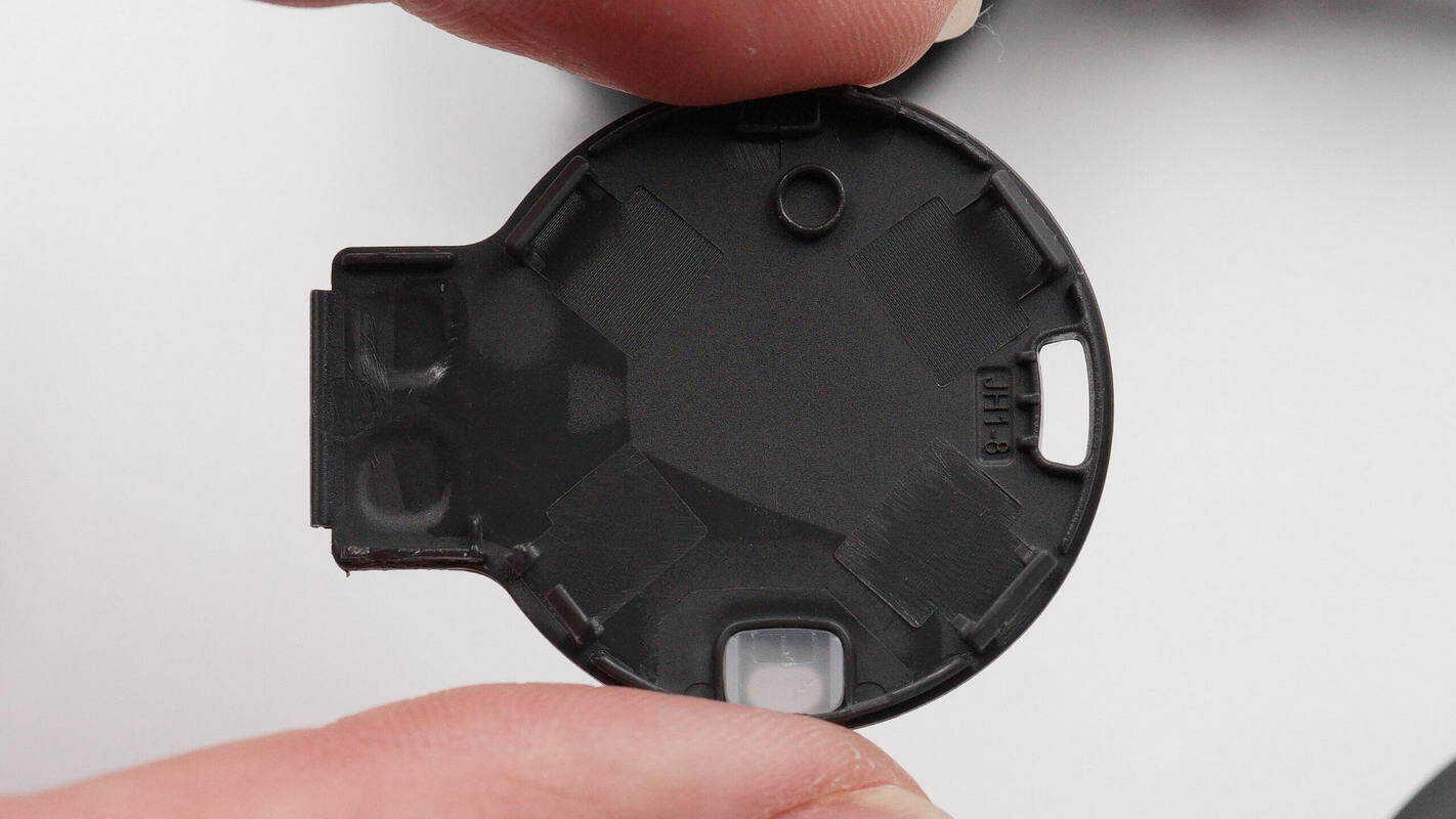
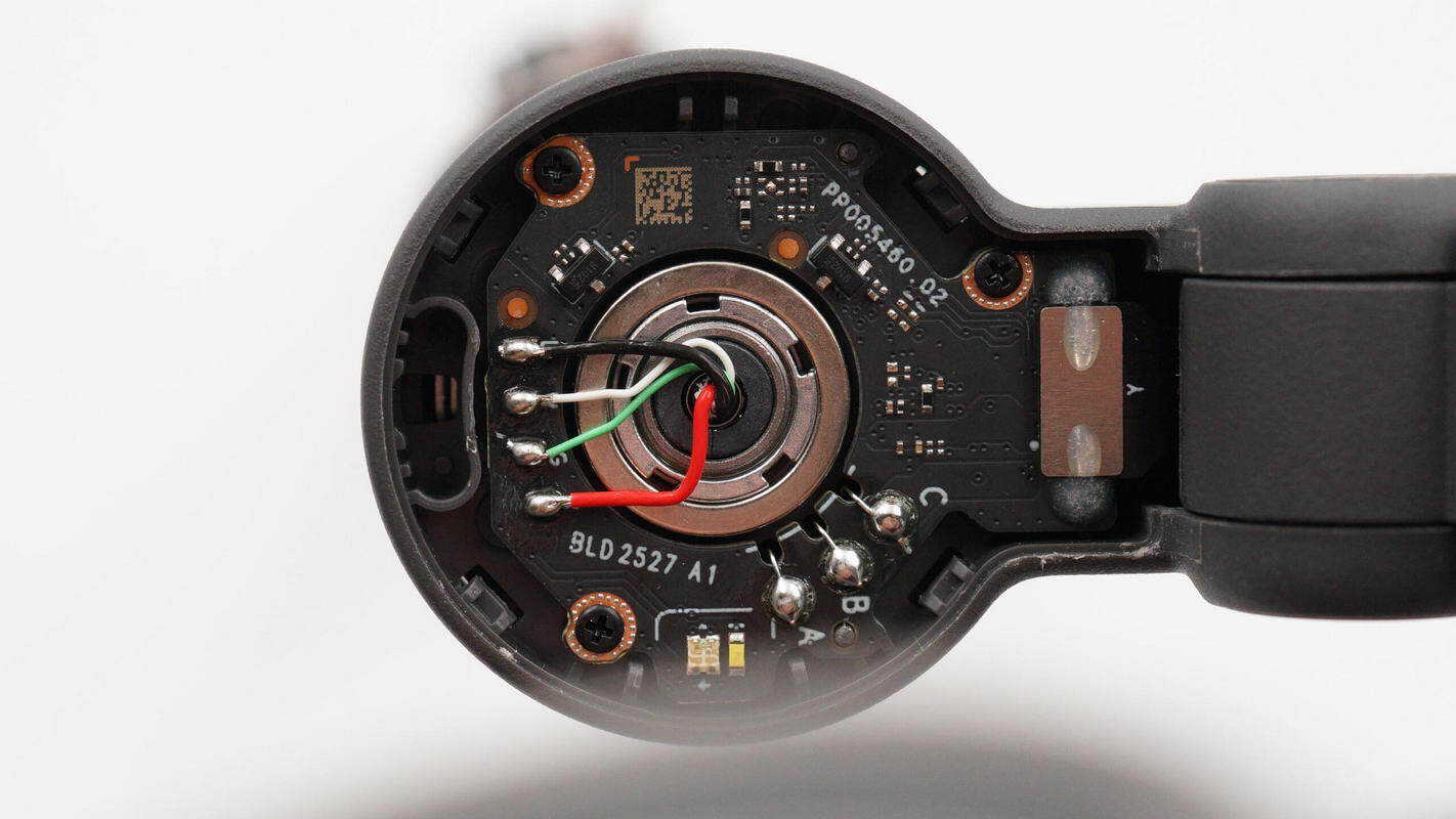
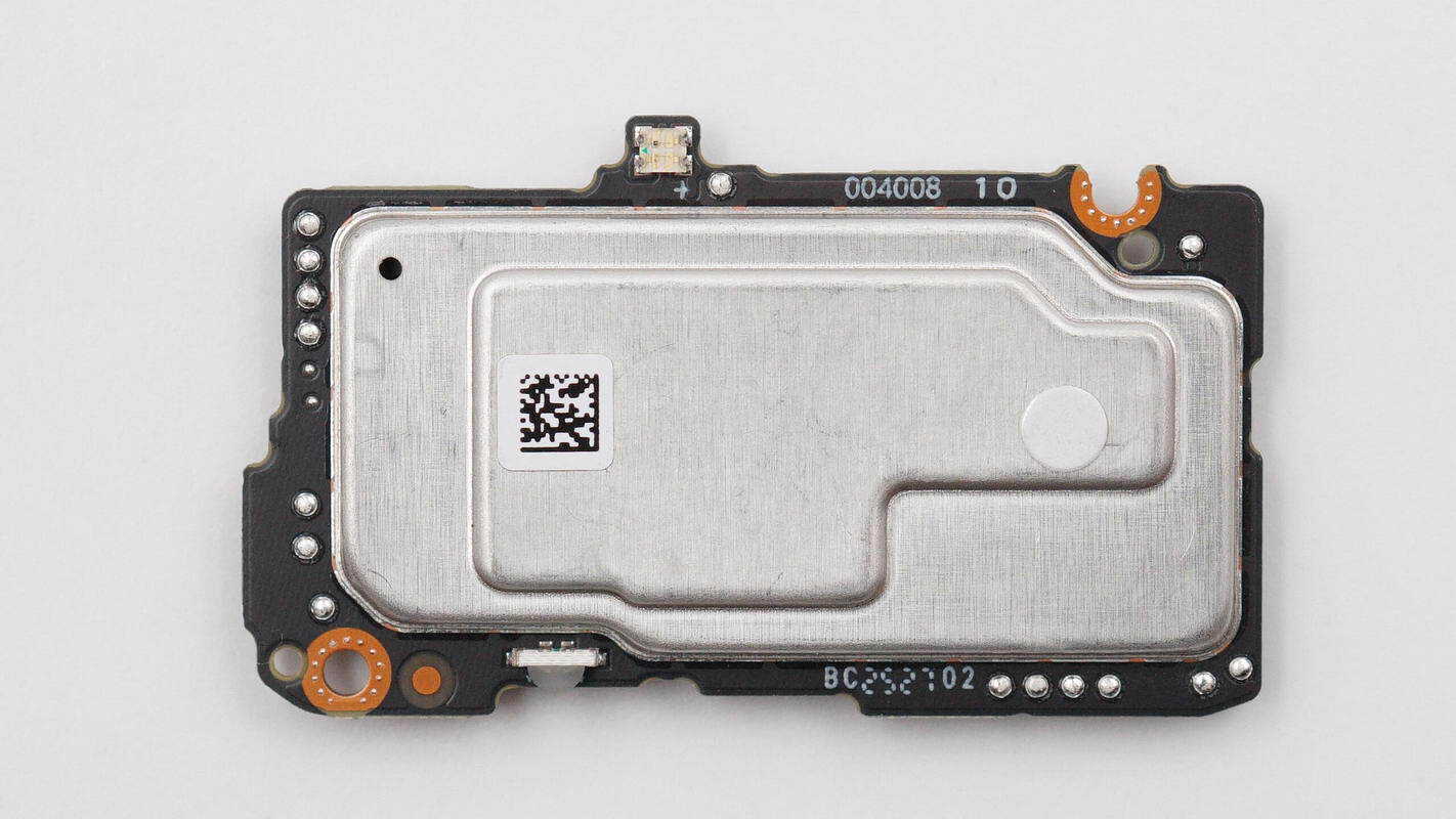
Remove the cover of the roll axis motor.
A light-transmitting window for the indicator LED is integrated into the inside of the cover.
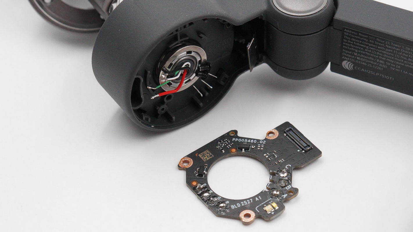
A PCB is installed inside and secured with screws, and the roll axis motor is connected via soldering.
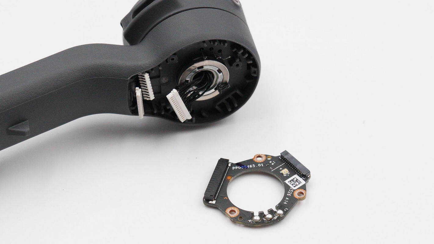
Separate the motor from the PCB.

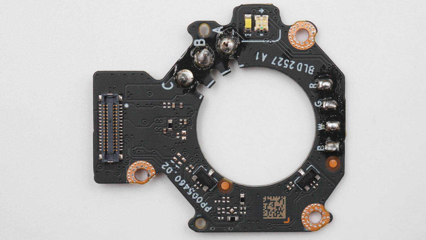
One side of the PCB is equipped with a connector and an LED indicator.
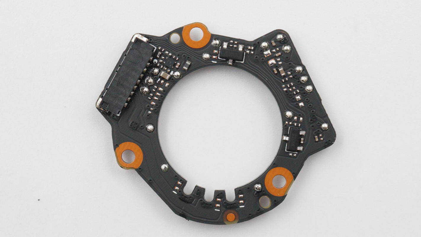
The other side has a soldered connector and a Hall sensor.
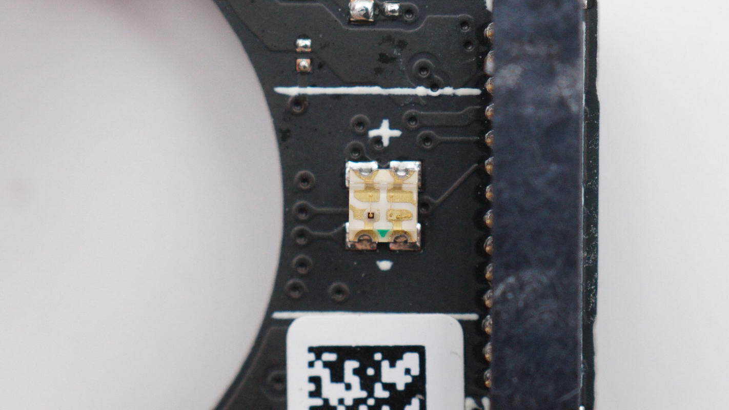
Close-up view of the surface-mounted LED indicator.
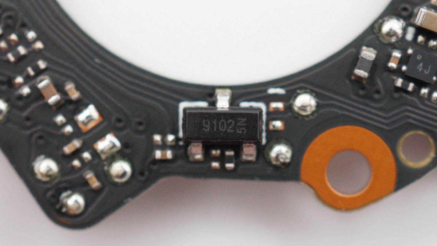
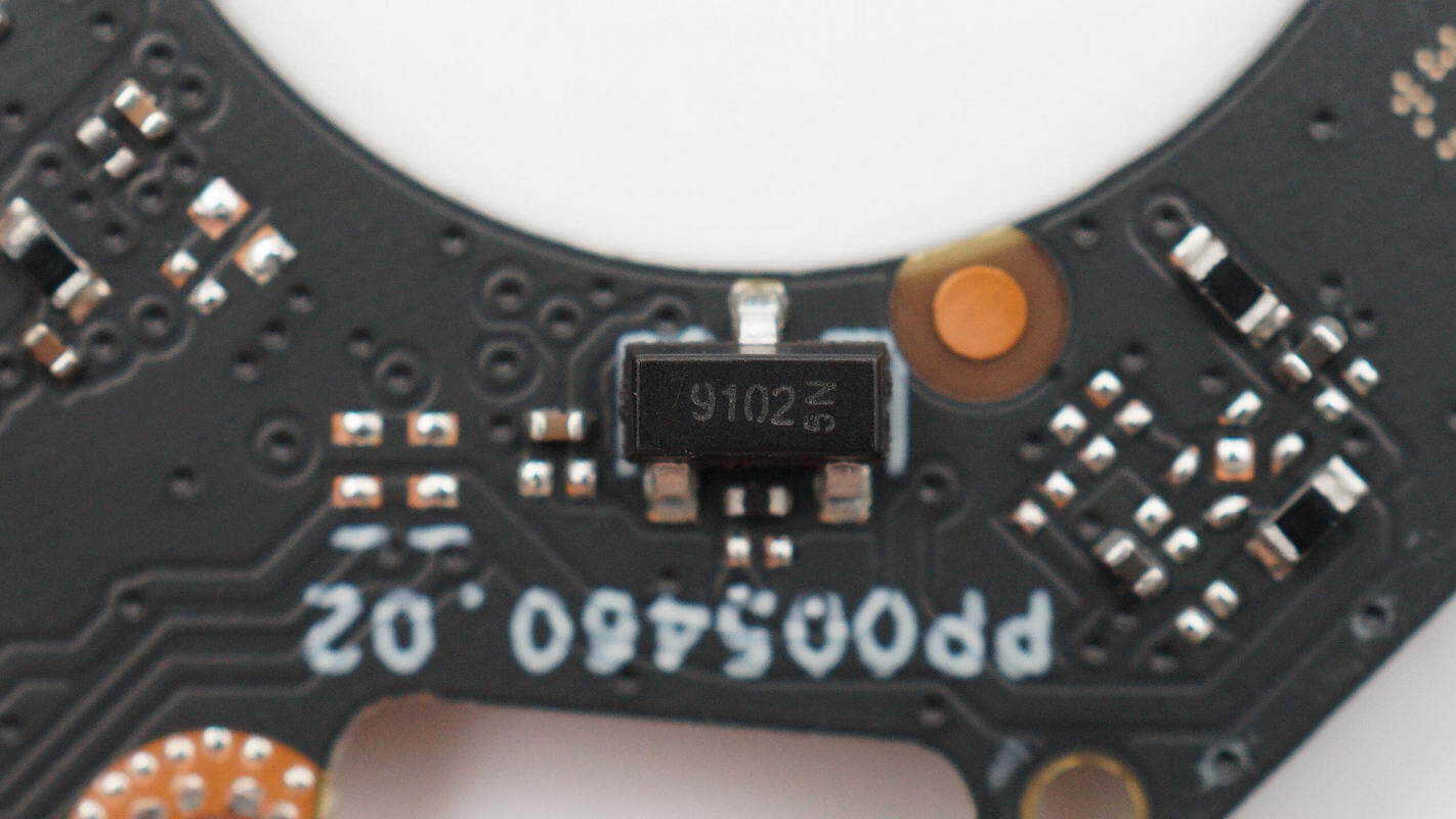
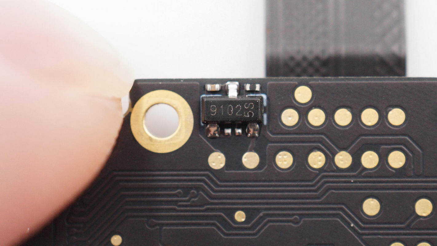
Two MagnTek MT9102 linear Hall sensors are used to detect the motor rotor angle.
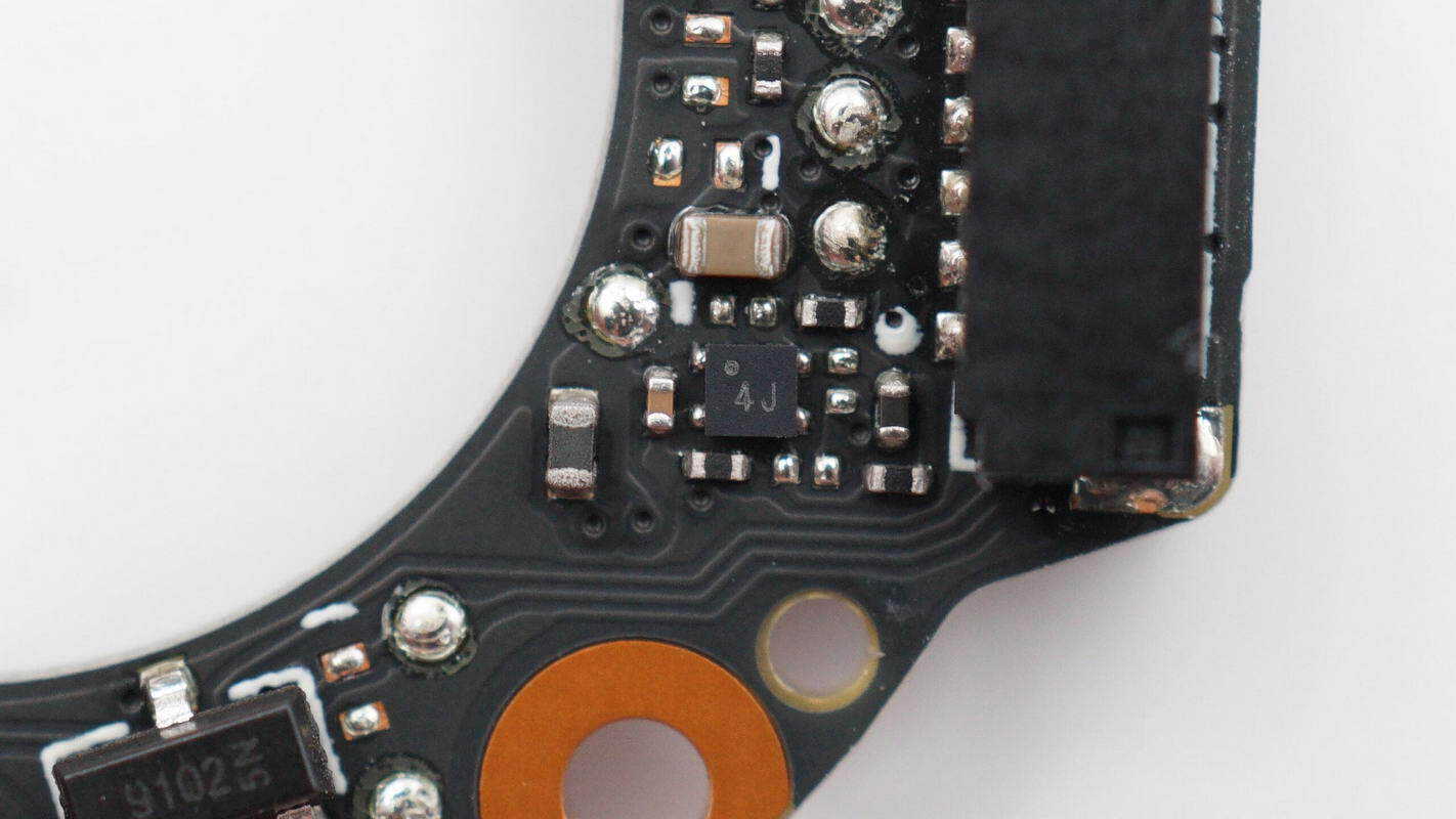
Close-up view of the chip marked with “4J”.
Remove the housing cover of the pitch axis motor.
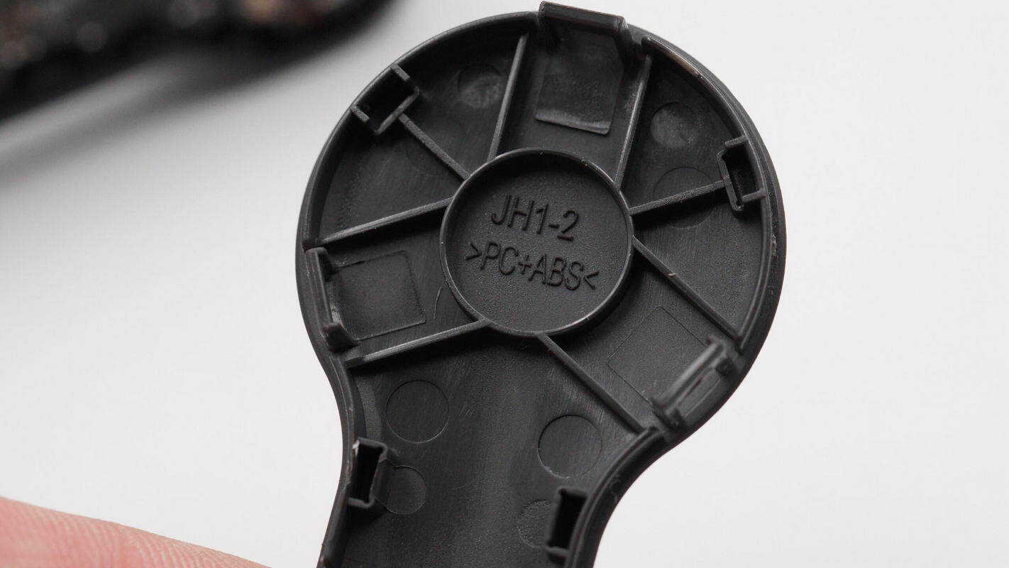
The cover is made of PC+ABS material.
Inside the housing is an elongated PCB secured with screws, and the pitch axis motor is connected via soldering.
Separate the motor from the PCB.
One side of the PCB includes an overcurrent protection switch, a motor driver IC, a buck converter IC, and a connector.

The other side includes an MCU, a motor driver IC, a synchronous buck converter IC, Hall sensors, and a power control MOSFET.
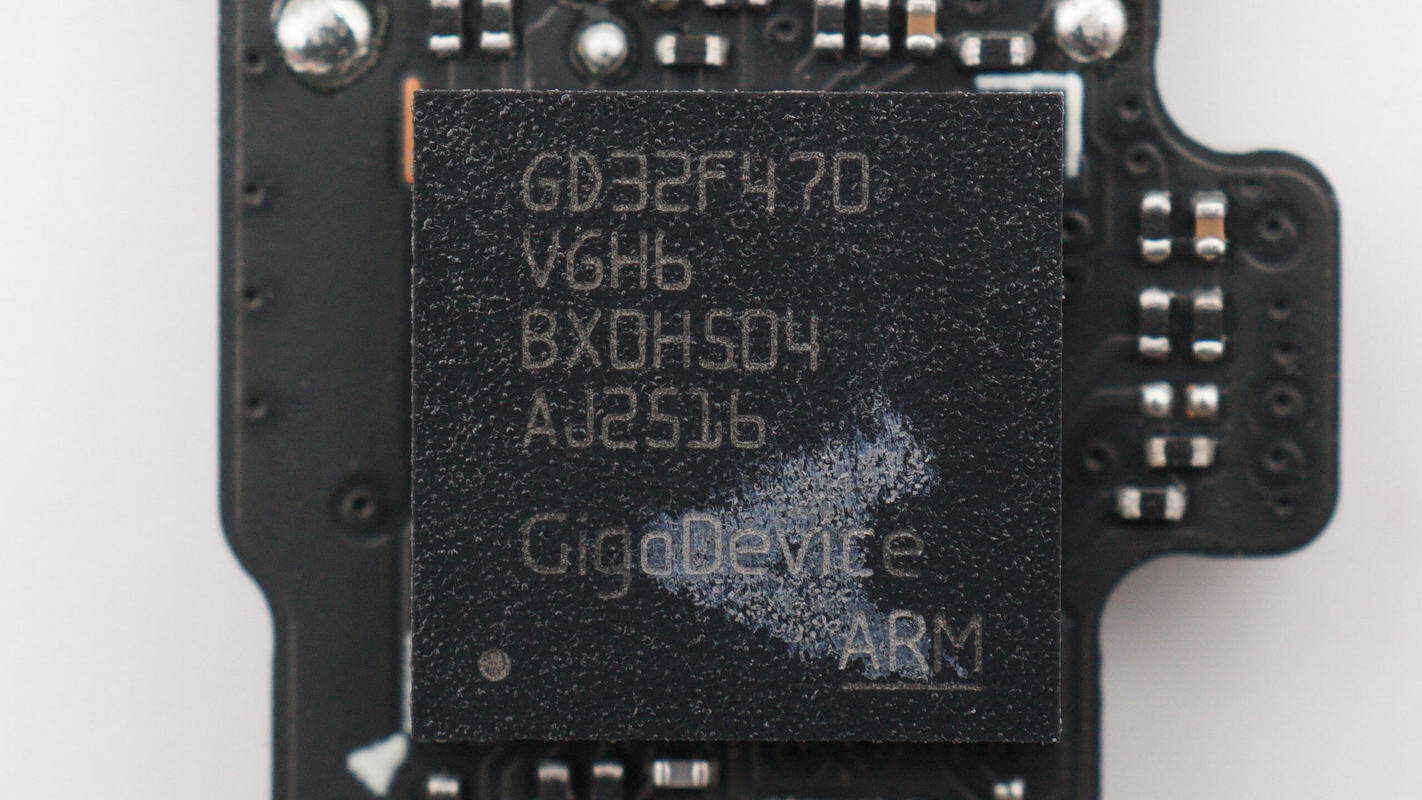
The main MCU is supplied by GigaDevice, model GD32F470VGH6. It integrates a Cortex-M4 core with a clock frequency of up to 240 MHz, includes FPU and DSP units, features 1 MB of embedded Flash and 512 KB of SRAM, provides comprehensive communication interfaces, and is packaged in a BGA100 form factor.

Close-up view of the 12.0 MHz clock crystal.
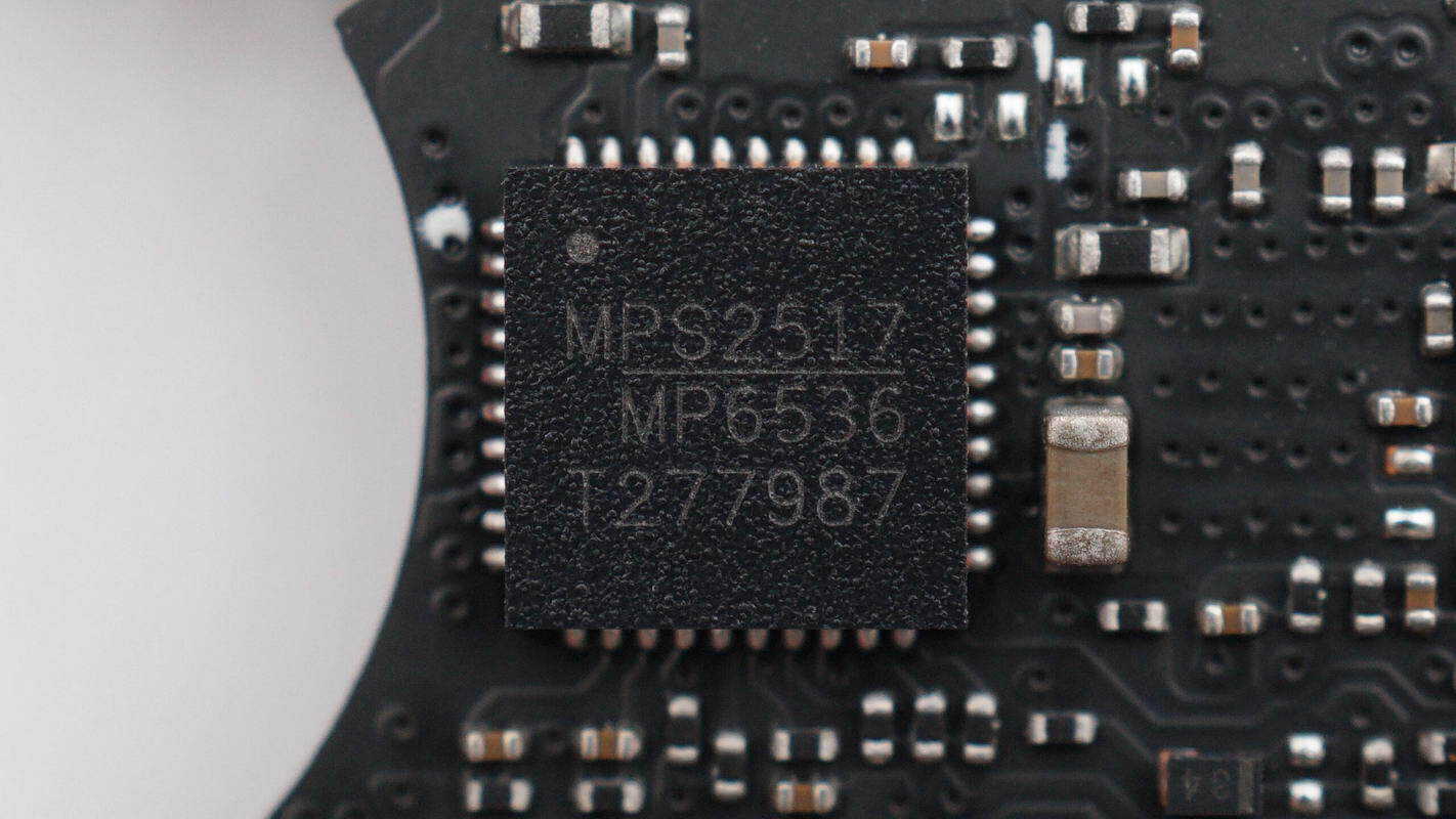
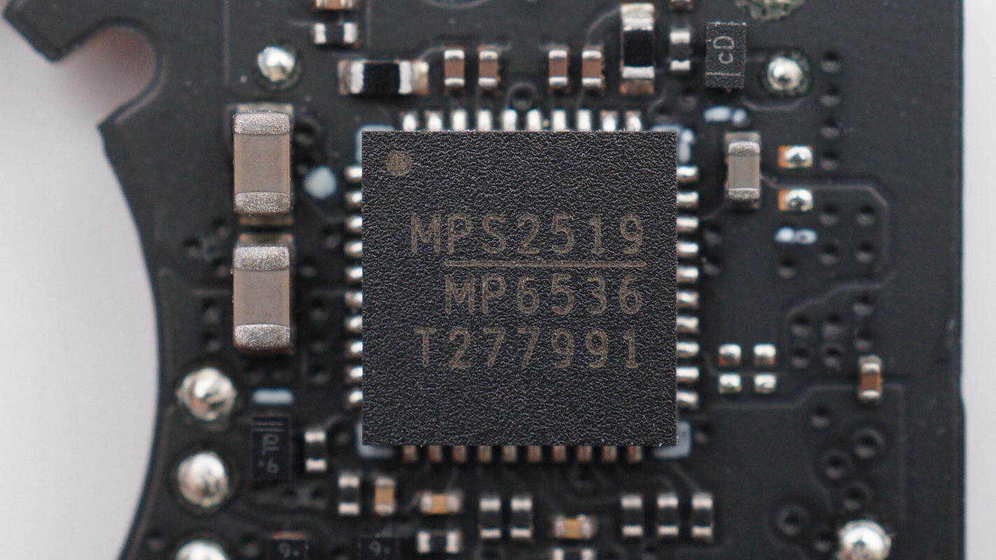
The motor driver IC is supplied by MPS, model MP6536. It is a three-channel half-bridge driver supporting an operating voltage range of 5–26 V, a peak output current of 5.5 A, and PWM frequencies up to 1 MHz. The internal power switches feature current limiting and include input undervoltage protection, thermal shutdown, and short-circuit protection. The device is designed for three-phase brushless motor applications and is packaged in a QFN-40 form factor.
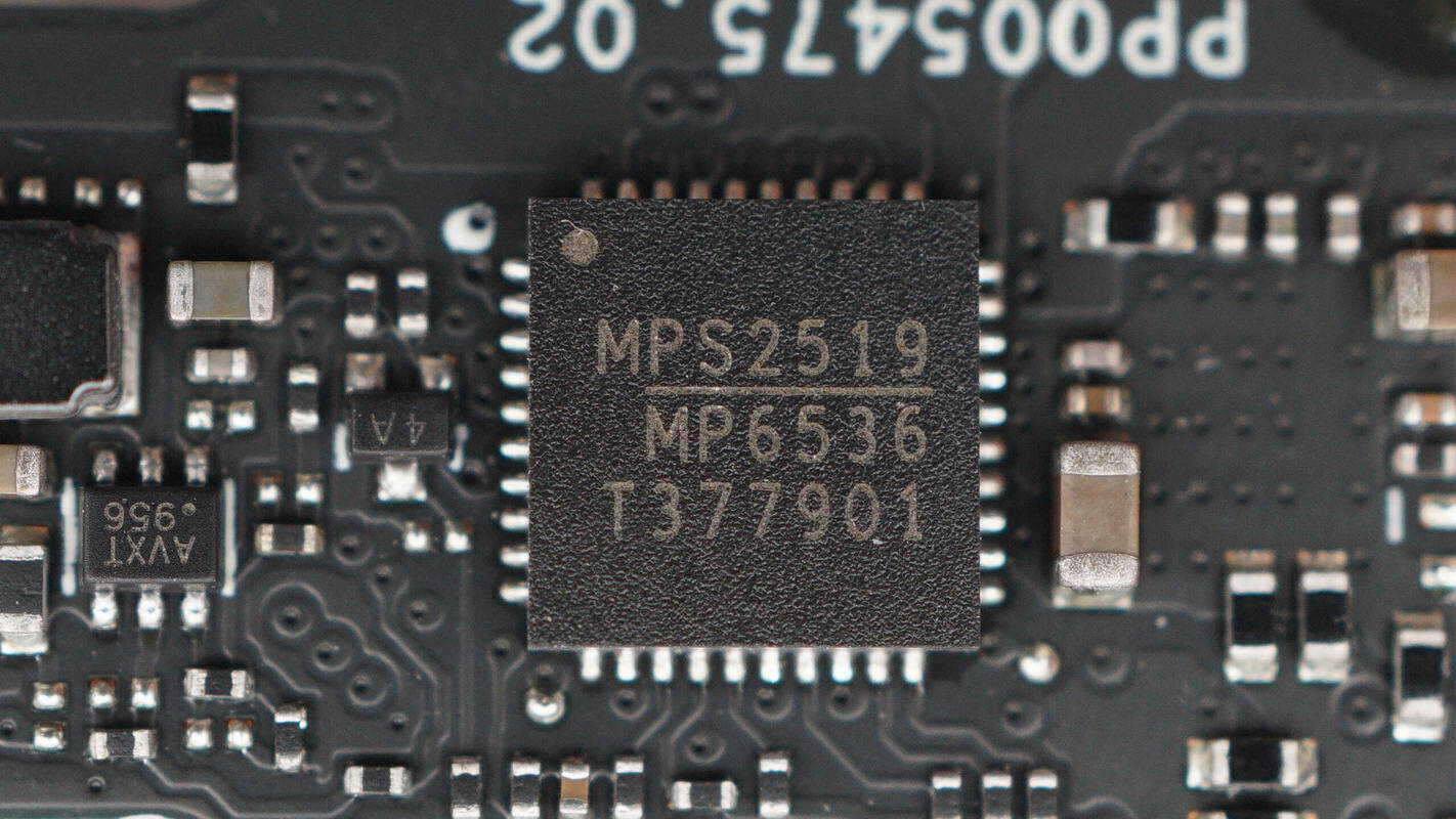
The other motor driver IC is of the same model.

The overcurrent protection IC is supplied by Silergy, marked with “Ye”, model SY6897A. It supports an operating voltage range of 2.5–16 V and adjustable current limiting from 1 A to 5 A, and is packaged in a 2 × 2 mm QFN form factor.
The other overcurrent protection IC is of the same model.
The synchronous buck converter IC is supplied by MPS, marked with “AVX”, and is packaged in an SOT-563 form factor.
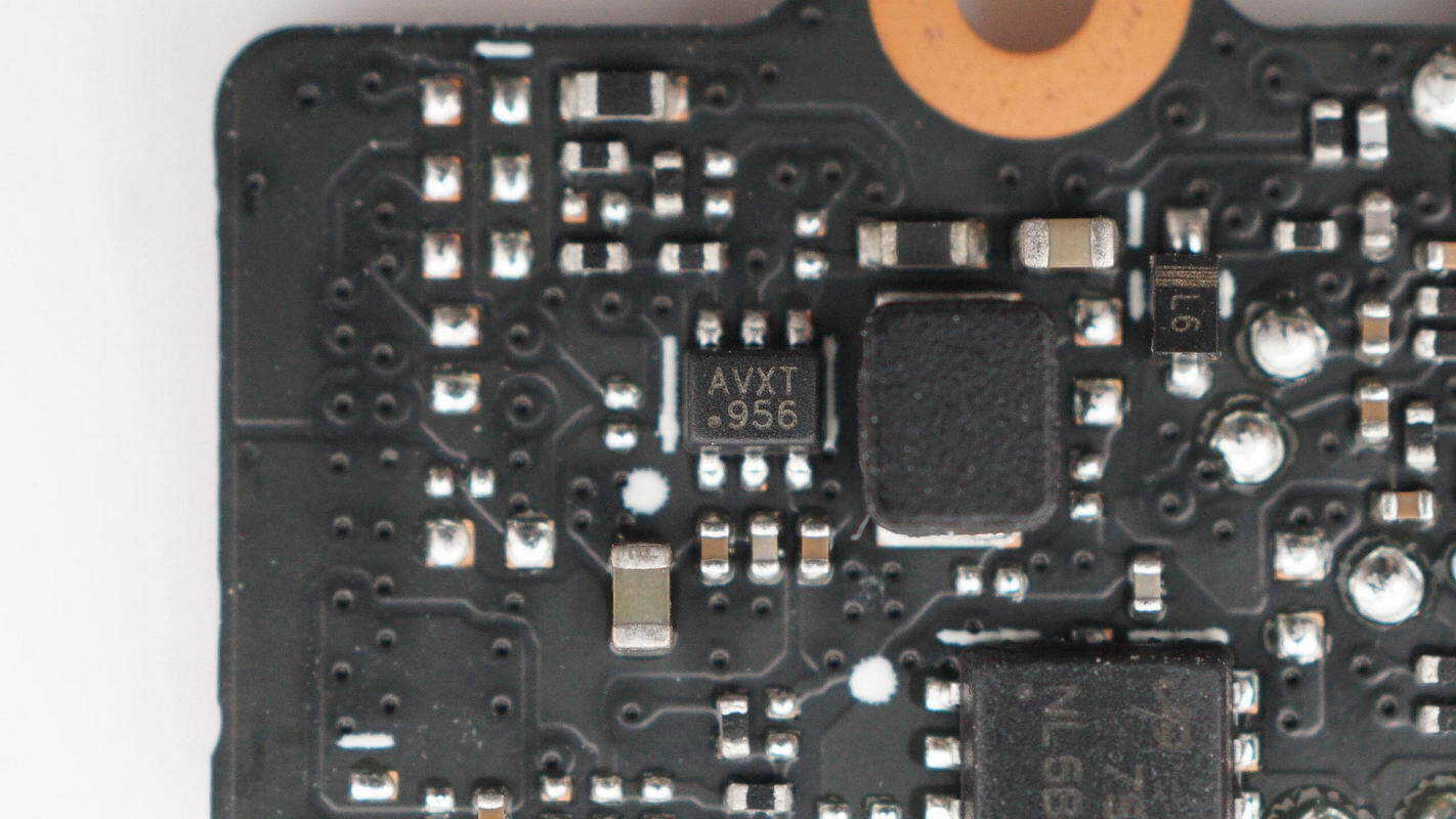
The other buck converter IC is of the same model.

The power control MOSFET is supplied by AOS, model AON7544. It is an N-channel MOSFET rated at 30 V, with an on-resistance of 4.1 mΩ, featuring low gate charge and high current capability, and is packaged in a DFN 3 × 3 EP form factor.
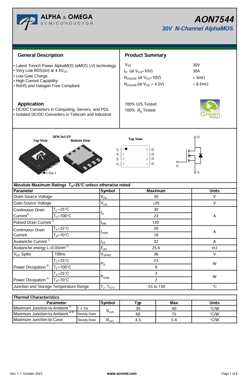
Here is the information about AOS AON7544.
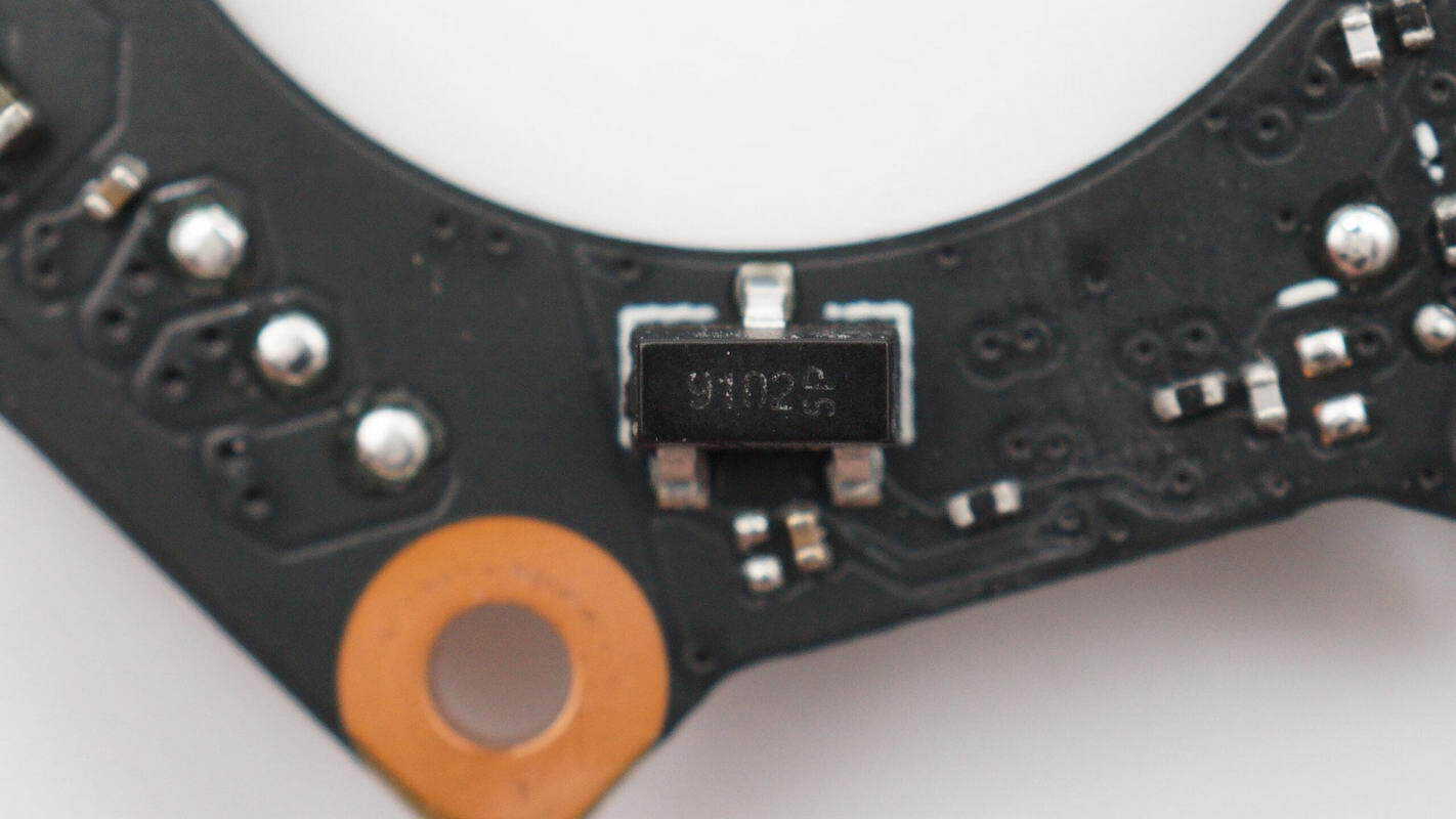
Two MagnTek MT9102 linear Hall sensors are used to detect the motor rotor angle.
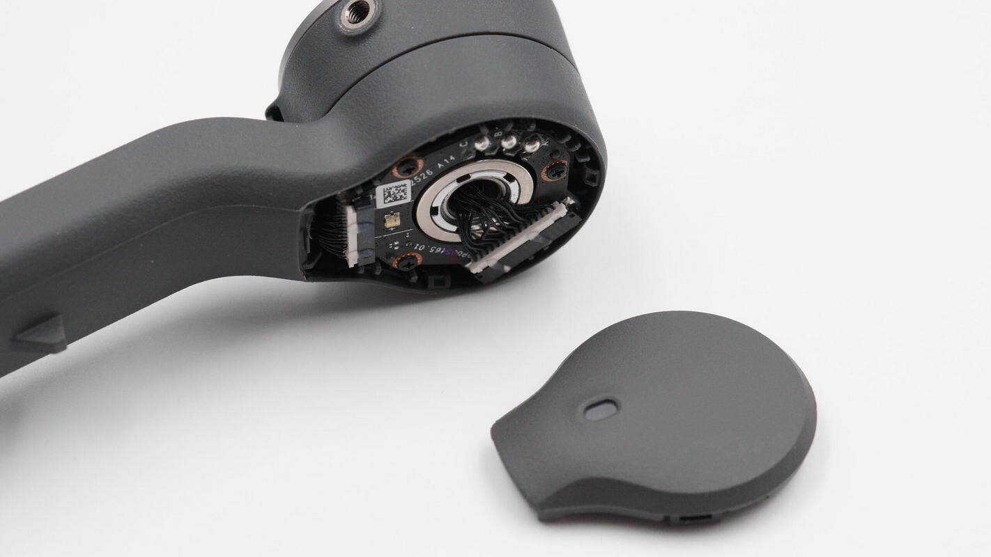
Finally, remove the housing cover of the pan axis motor.
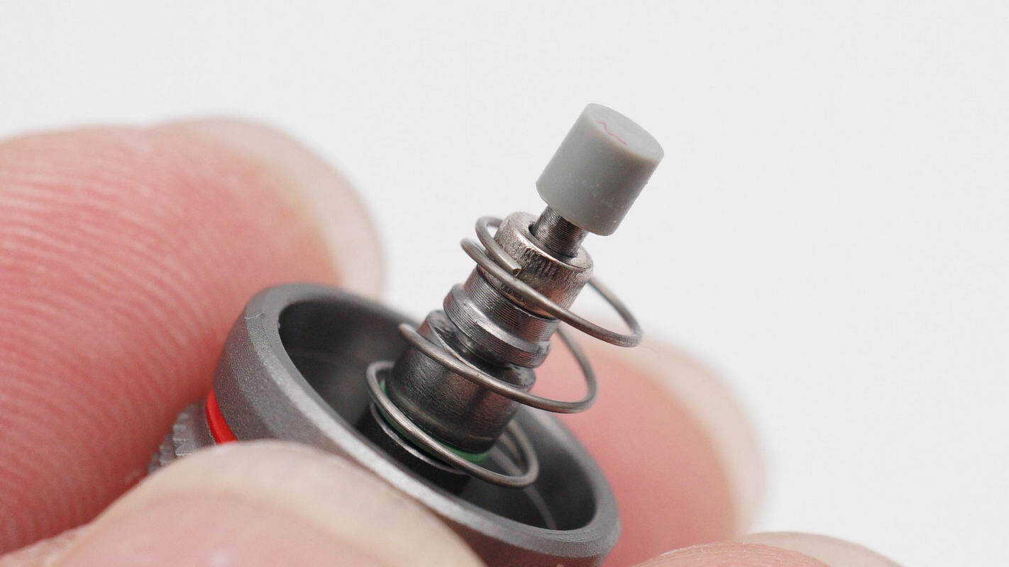
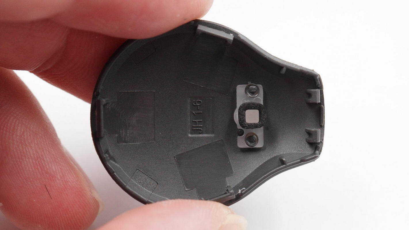
The cover features openings for the indicator LED and the positioning pin.
The positioning pin is spring-loaded for return.
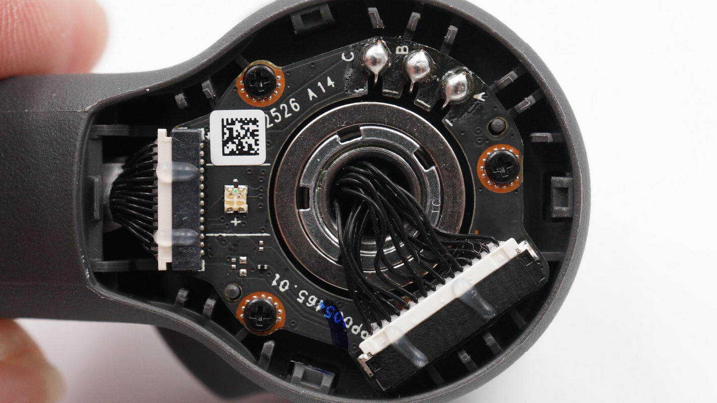
A PCB is installed inside and secured with screws, and the pan-axis motor is connected via soldering.
Separate the motor from the PCB.
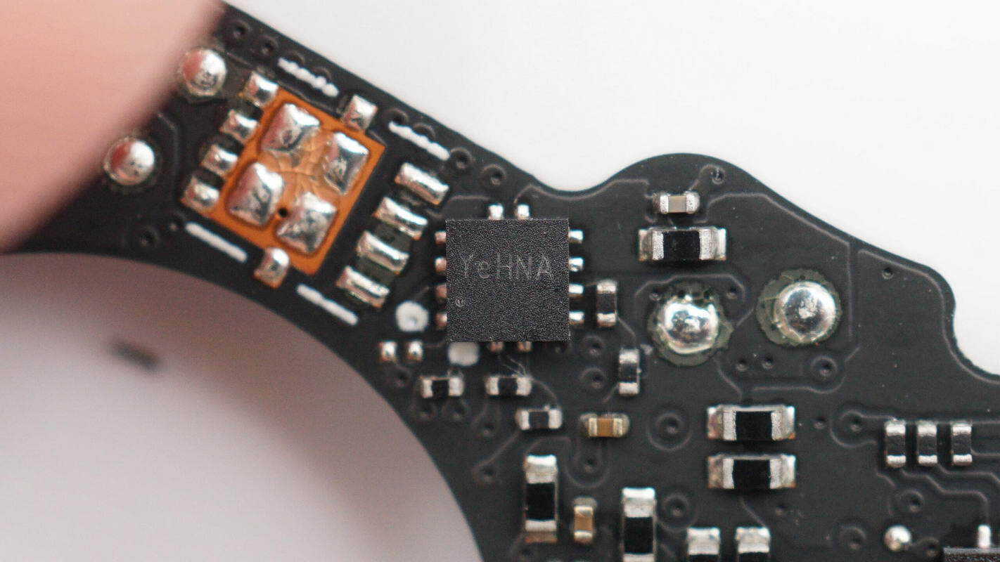
One side of the PCB includes a connector, Hall sensors, and an LED indicator.
The other side has the motor driver IC soldered in place.
The motor driver IC used is the MPS MP6536.
Two MagnTek MT9102 linear Hall sensors are used to detect the motor rotor angle.
Close-up view of the LED indicator.
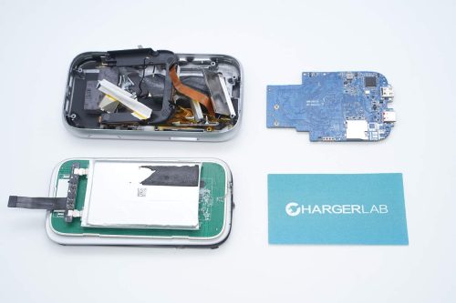
Finally, disassemble the OM multifunction tracking module by separating the housing along the seam.
An aluminum alloy heat sink is installed inside the tracking module cover.
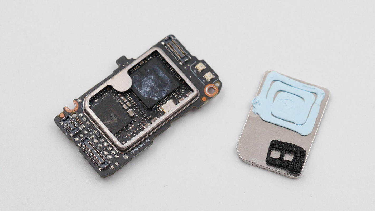
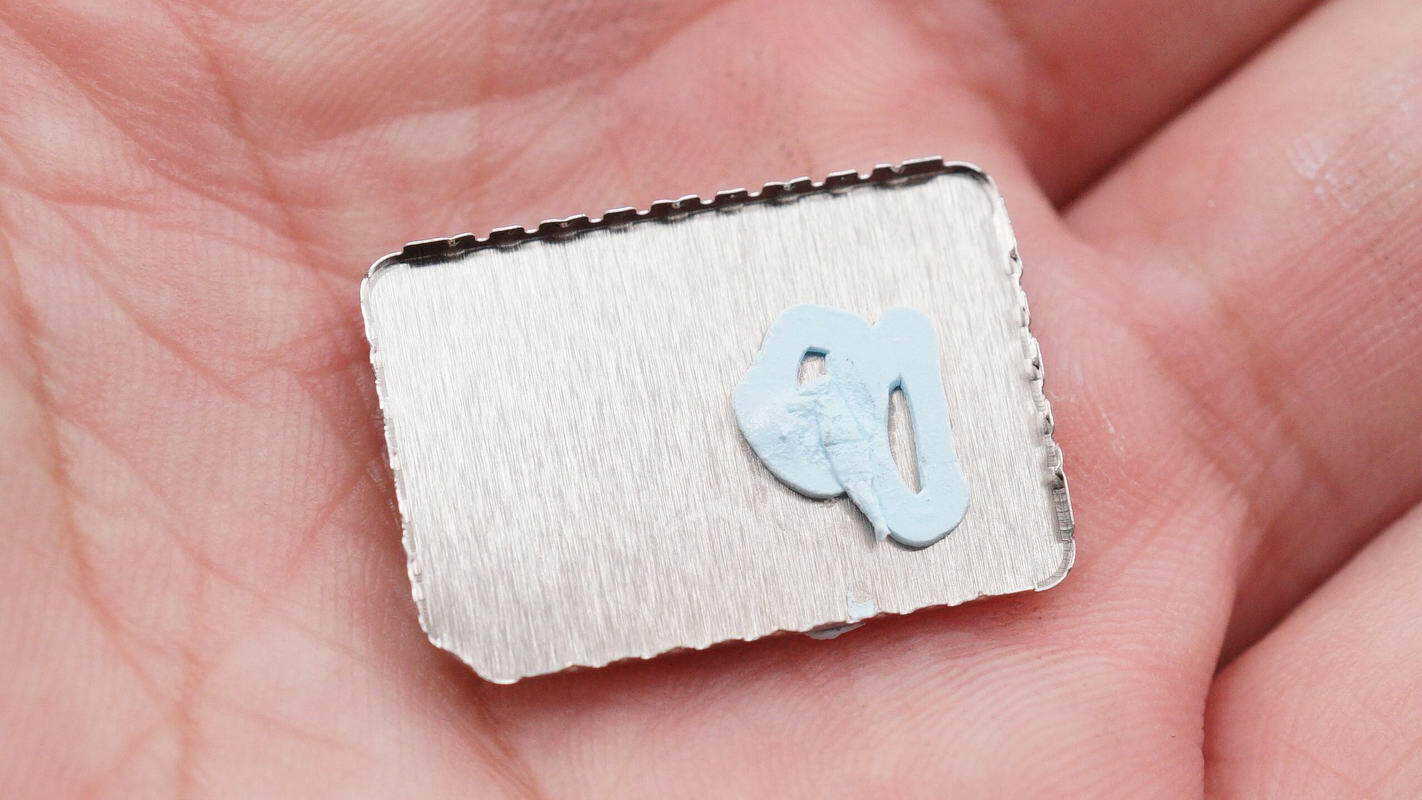
Inside the tracking module housing is a PCBA module, with a large-area shielding cover on top that is coated with thermal grease.
Remove the screws and detach the upper PCBA module; another PCBA module is installed at the bottom.
Remove the lower PCBA module. Graphite thermal pads are applied to the rear of the fill light and the camera for heat dissipation.
The rubber pads are installed inside the button for cushioning.
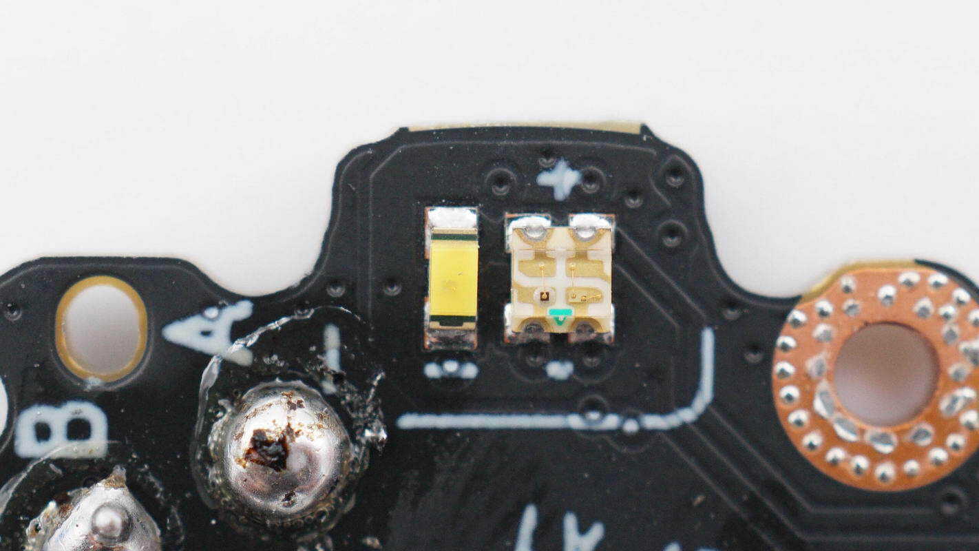
Close-up view of the graphite thermal pads attached to the rear of the fill light and the camera.
Remove the shielding cover from the PCBA module.
The inside of the shielding cover is coated with thermal compound.
Inside the shielding cover are the main controller IC and the flash memory IC. Connectors and a microphone indicator LED are located on both sides.
A shielding cover is installed on the rear of the PCBA module and is secured by soldering.
Cut open the shielding cover. Inside are a synchronous buck converter IC and an LED driver IC, with LED indicators located on both sides.
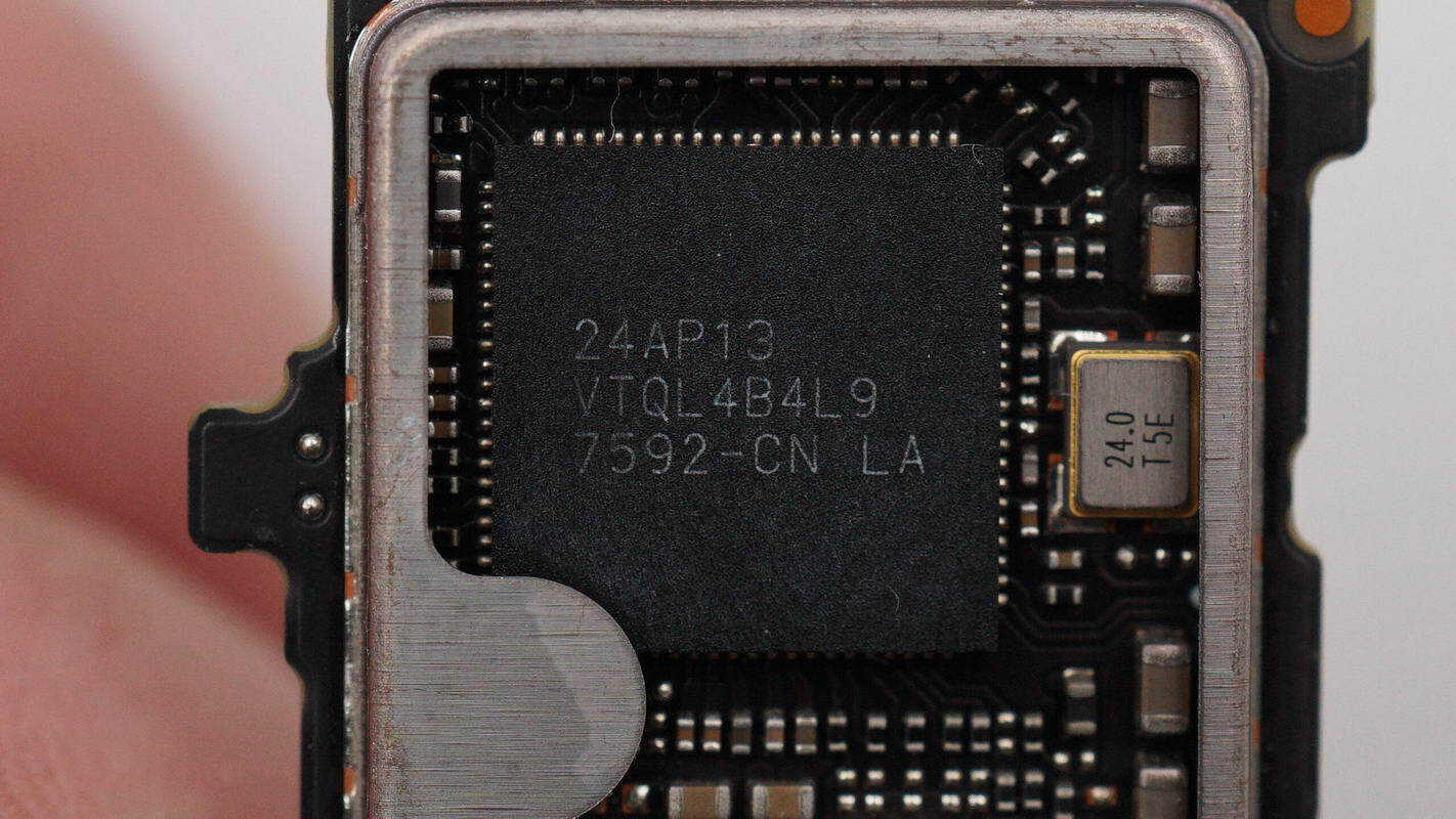
The master controller IC is marked “24AP13 VTQL4B4L9 7592-CN LA” and is packaged in a QFN-88 form factor.
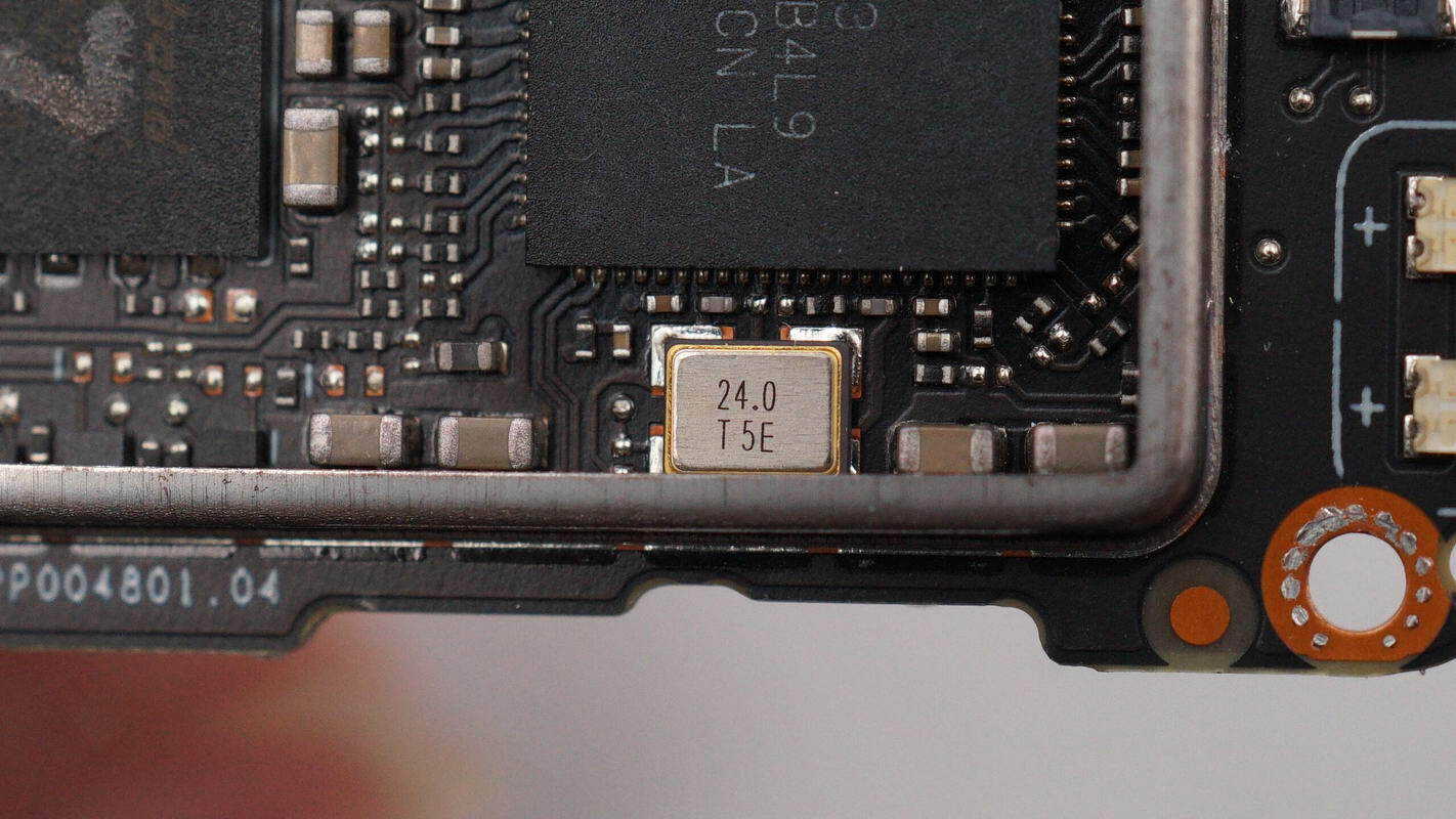
Close-up view of the external 24 MHz clock crystal.
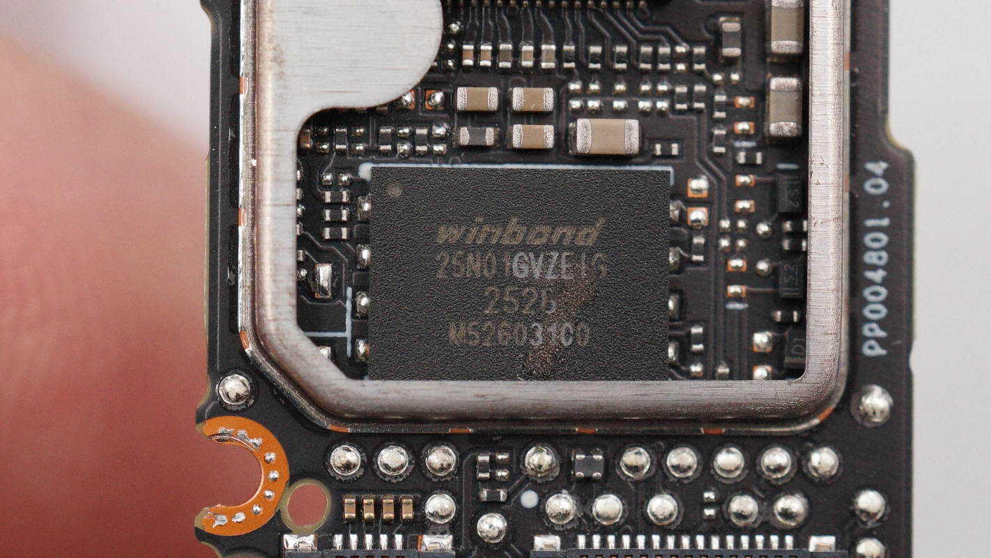
The memory IC is supplied by Winbond, model W25N01GVZEIG. It is a 128 MB SLC flash memory device supporting an operating voltage of 2.7–3.6 V, featuring an SPI interface, and packaged in a WSON-8 form factor.
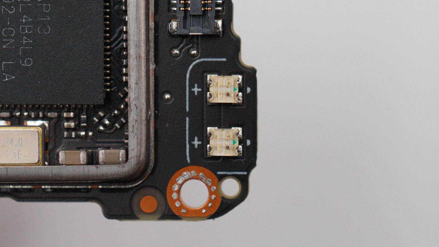
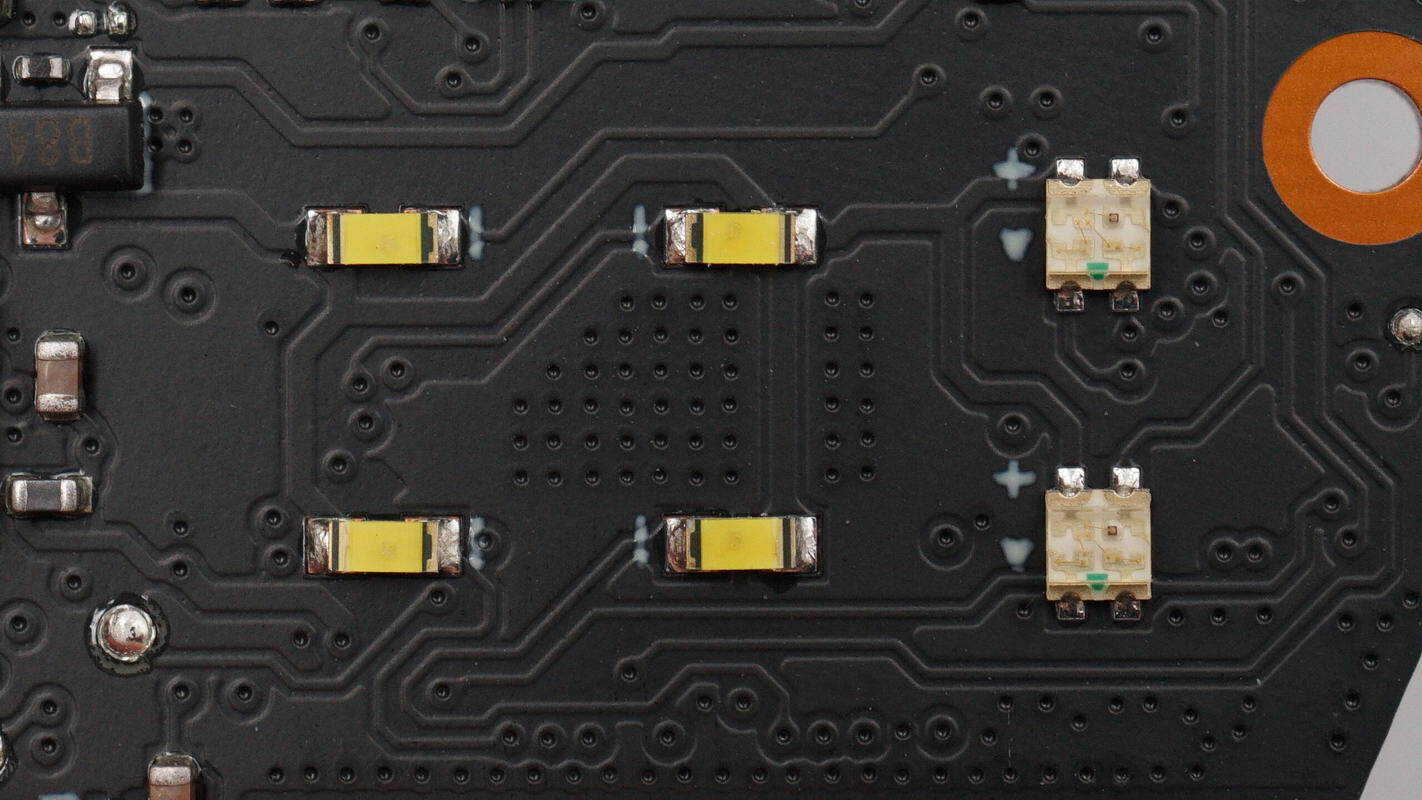
Close-up view of the two microphone indicator LEDs.
The LED driver IC is supplied by SGMICRO, model SGM3749. It is a boost LED driver supporting PWM dimming, operates with input voltages up to 20 V, features a switching frequency of 1.25 MHz, and is packaged in a TDFN 2 × 2 mm 6-lead form factor.
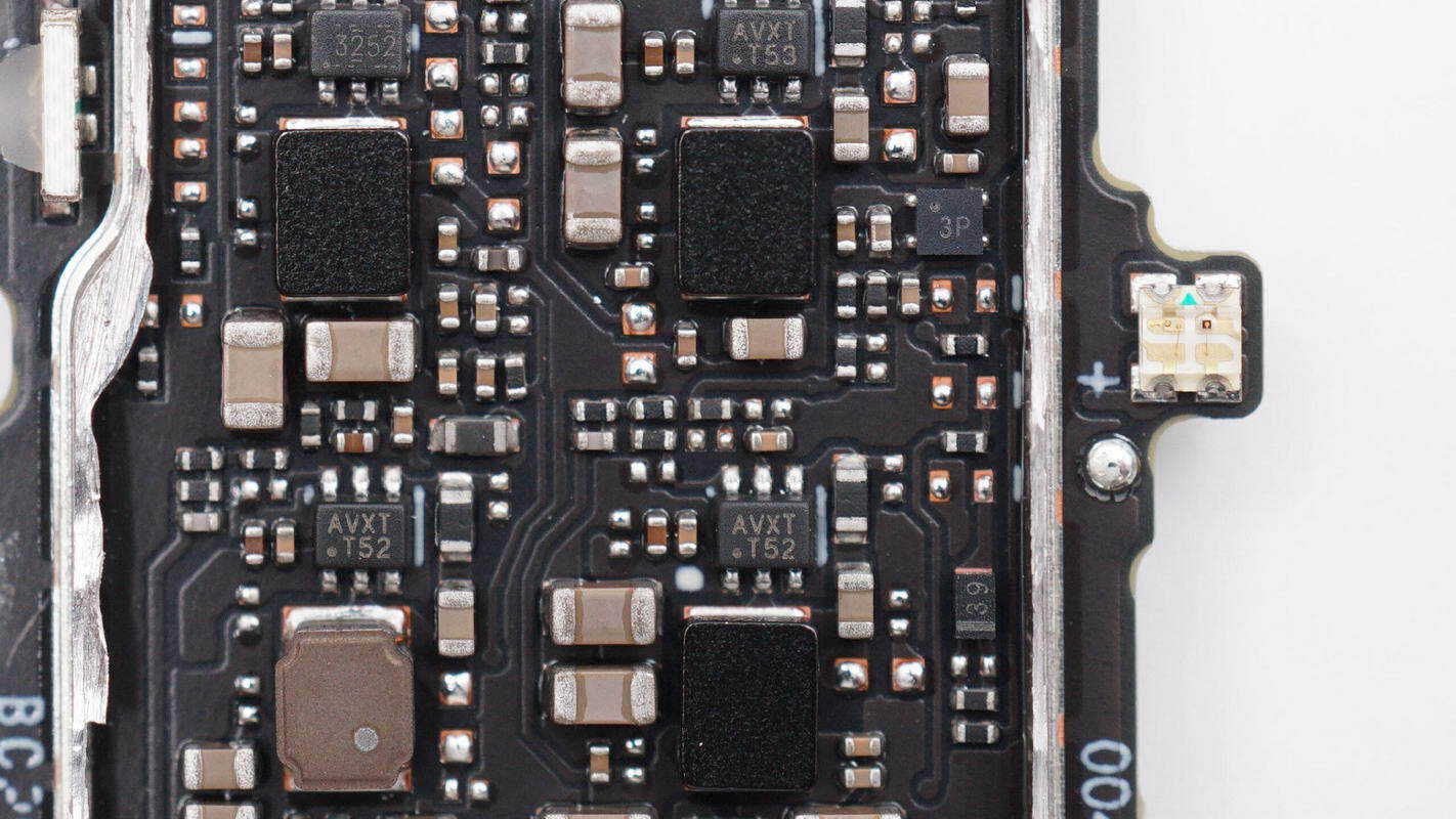
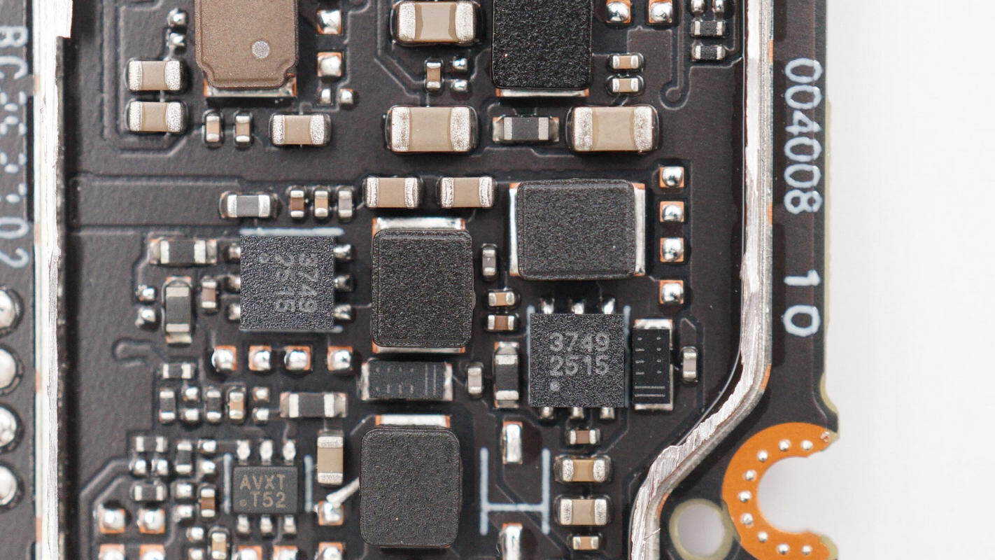
The rear side of the PCB is populated with four buck chips. The one located at the upper left is supplied by Texas Instruments, marked with “3252”, model TPS563252. It is a synchronous buck converter supporting an input voltage range of 3–17 V with a 3 A output current and is packaged in an SOT-563 form factor. The remaining three converters are all supplied by MPS and are marked with “AVX”.

An additional buck chip marked with “AVX” is also located at the lower right corner.
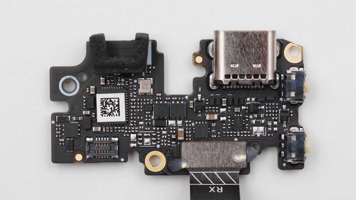
The lower PCBA module integrates a Bluetooth SoC, a power control MOSFET, and an overcurrent protection IC. A USB-C receptacle and a tactile switch are also located on the right side.

A MOSFET is installed on the rear side.
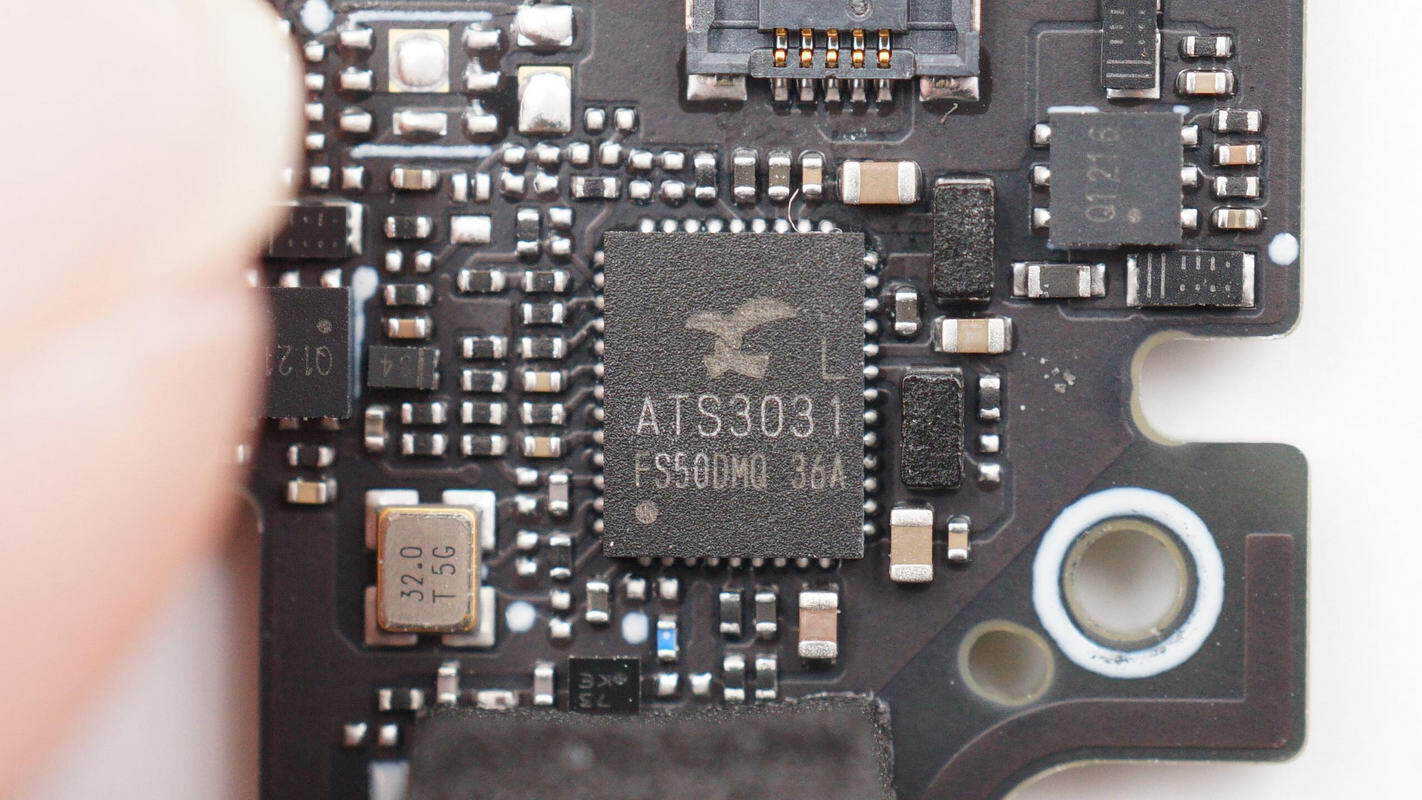
The Bluetooth SoC is supplied by Actions, model ATS3031L. It is a highly integrated single-chip SoC featuring an ARM Cortex-M4F processor with an integrated FPU, operating at up to 128 MHz, and an integrated DSP running at 170 MHz. It is suitable for Bluetooth transceivers, wireless microphones, low-latency wireless gaming headsets, and wireless communication headsets and is packaged in a QFN-44 form factor.
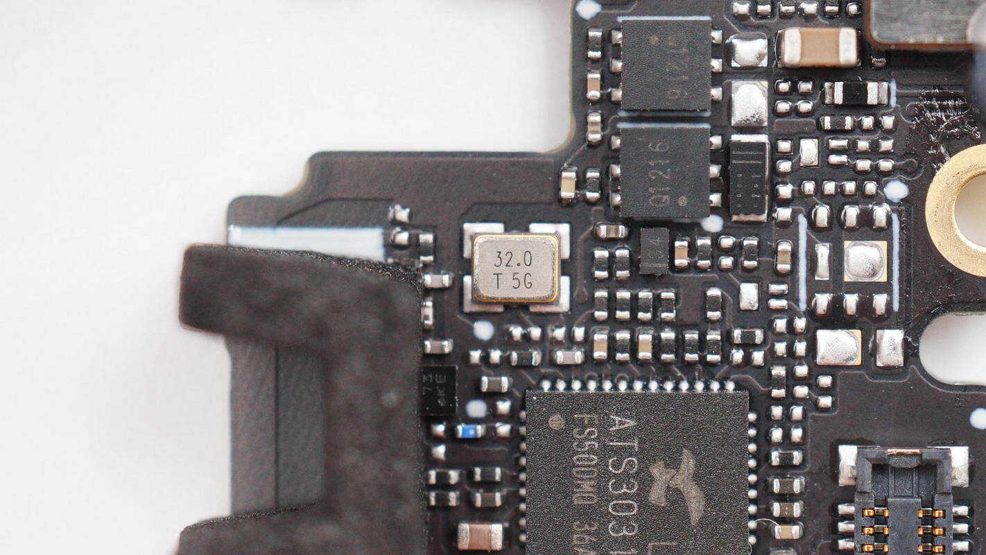
Close-up view of the 32.0 MHz clock crystal.
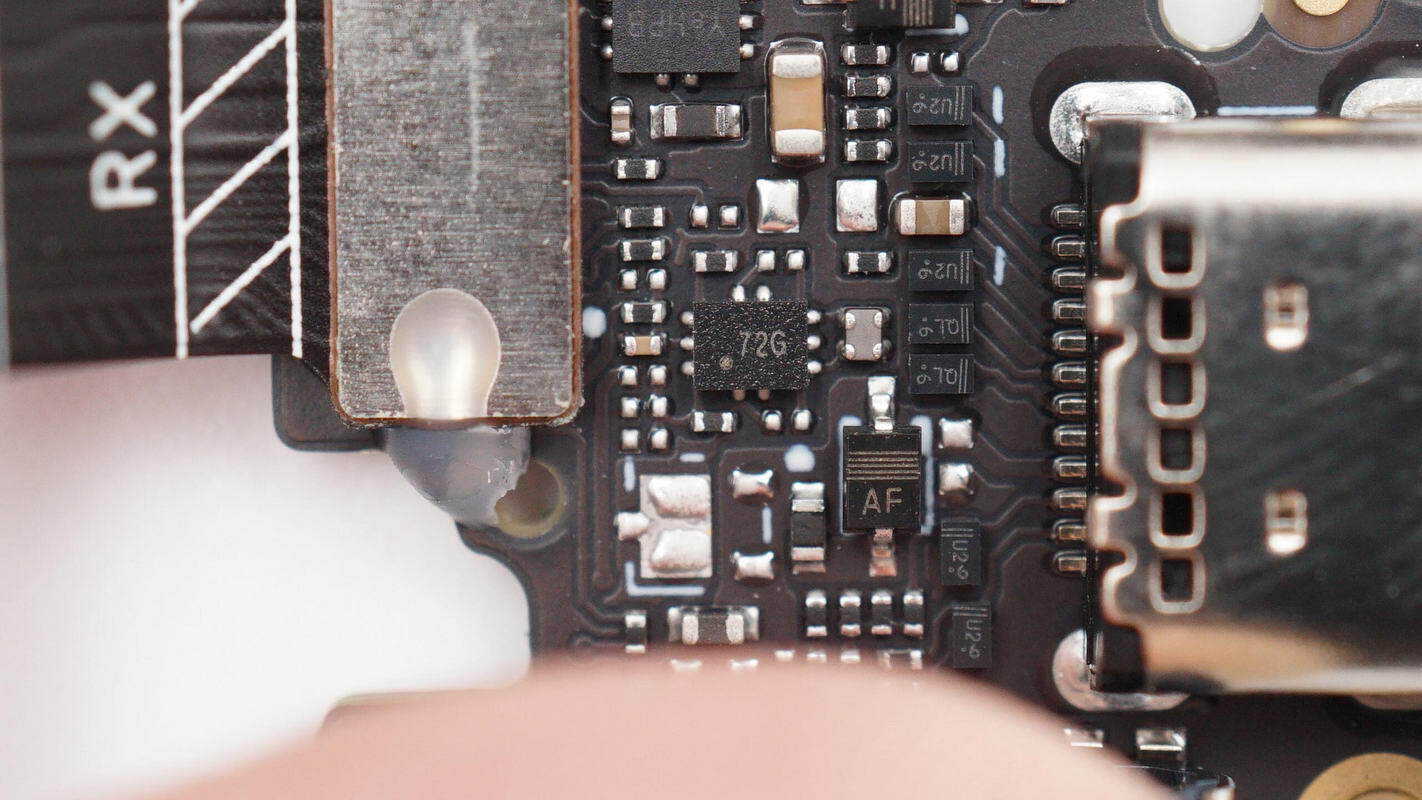
Close-up view of the toggle switch marked with “72G”.
The MagnTek MT9102 linear Hall sensor is used to detect the module position.
The overcurrent protection IC used is the Silergy SY6897A.

The power control MOSFET is supplied by Vergiga, model VS3510AE. It is a P-channel MOSFET rated at −30 V with an on-resistance of 10 mΩ and is packaged in a PDFN 3 × 3 mm form factor.
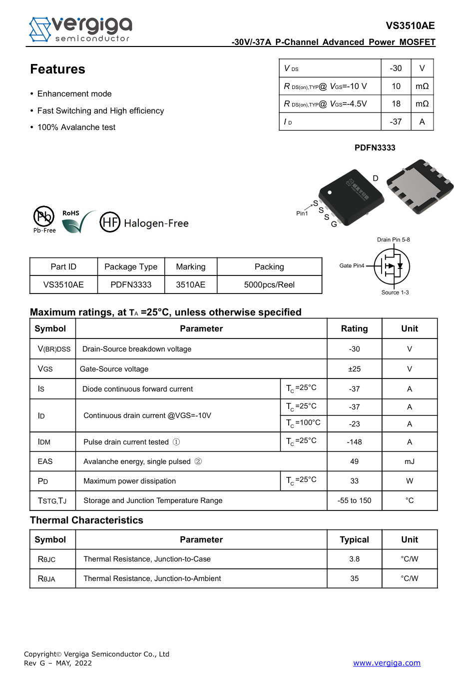
Here is the information about Vergiga VS3510AE.
Two power control MOSFETs are supplied by YJ, marked with “Q1216”, model YJQ1216A. They are P-channel MOSFETs rated at −20 V with an on-resistance of 11 mΩ and are packaged in a DFN2020-6L 6-lead form factor.
Close-up view of the two tactile switches on the side.
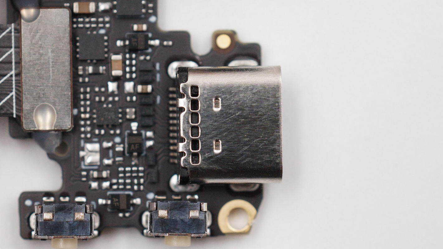
The USB-C socket is secured by through-hole soldering.
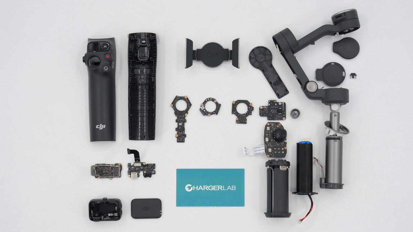
Well, those are all components of the DJI Osmo Mobile 8.
Summary of ChargerLAB
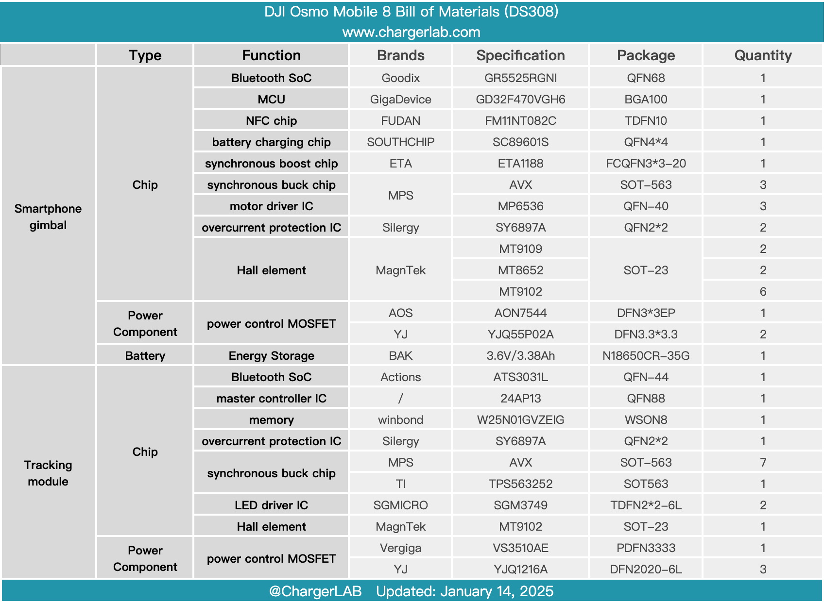
Here is the component list of the DJI Osmo Mobile 8 for your convenience.
The gimbal integrates an extension rod and a tripod in a single structure and features a three-axis design, supporting pan, tilt, and roll movements. It enables 360° unlimited horizontal rotation, lossless stabilization, and seamless switching between low-angle and high/low shooting positions. The gimbal charges via a USB-C port and is equipped with a built-in 3350 mAh battery, providing up to 10 hours of operating time and supporting smartphone charging. A joystick and a control wheel are integrated into the handle, significantly enhancing the user experience.
After taking it apart, we found that it features a built-in BAK 18650 battery with a capacity of 3.38 Ah. The handle integrates a Goodix GR5525RGNI Bluetooth SoC and a GigaDevice GD32F470VGH6 MCU, paired with a SouthChip SC89601S charging IC and an ETA ETA1188 boost converter. NFC functionality is implemented using the Fudan FM11NT082C controller.
The three-axis brushless motors are driven by MPS MP6536 motor driver ICs, with MagnTek MT9102 Hall sensors used for rotor position detection. The tracking module integrates an Actions ATS3031L Bluetooth SoC, powered by buck converters from MPS and Texas Instruments, and receives power from the gimbal through contact connections. The gimbal handle battery is protected by a plastic sleeve, and all FPC connectors are reinforced with adhesive. Overall, the internal construction is robust, and the build quality is reliable.
Related Articles:
1. Teardown of Bull 22.5W 10000mAh Semi-Solid State Power Bank (GNV-PGA10EB)
2. Teardown of Baseus 100W 7-in-1 Charging Station (E0307A)
3. Teardown of MIIIW 45W Mini Magic Cube GaN Charger (iCA4501)