Introduction
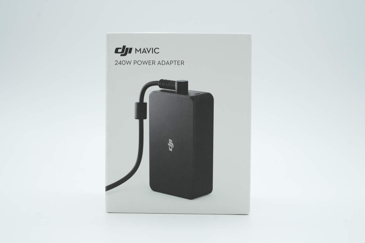
On May 13, DJI officially released its latest flagship consumer drone, the Mavic 4 Pro. Compared to the previous generation, it features significant improvements in imaging, flight performance, and intelligent control, making it especially suitable for professional users who demand top-tier image quality and advanced functionality.
The DJI Mavic 4 Pro is powered by a 6654mAh battery, offering up to 51 minutes of flight time. It comes equipped with a high-powered 240W GaN power adapter, which, when used in conjunction with the multi-battery charging hub, can simultaneously charge up to three Intelligent Flight Batteries in parallel. This greatly reduces charging time, allowing users to fully recharge their batteries during short breaks, ensuring sufficient power for continued use, and significantly improving the outdoor aerial photography experience.
Additionally, this power adapter features a USB-C port and supports a range of fast charging protocols, including UFCS, PD 3.1, and PPS, delivering up to 140W of fast charging power. This design enables the adapter to quickly charge other devices that support the PD protocol, eliminating the need to carry extra chargers when traveling and reducing overall gear load for users.
Let’s now take a closer look at the internal design and components.
Product Appearance
The front of the packaging features the DJI logo, the product name, and an image of the device.
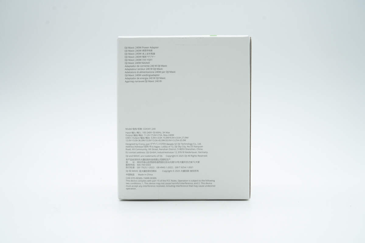
The spec info is printed on the back.
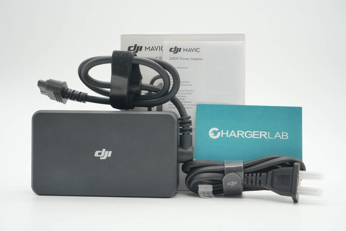
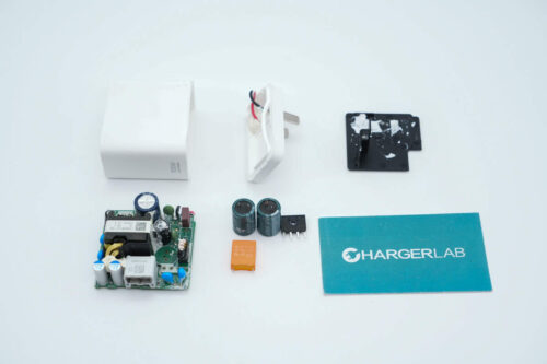
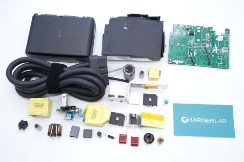
The packaging contains the power adapter, power cord, and some documents.
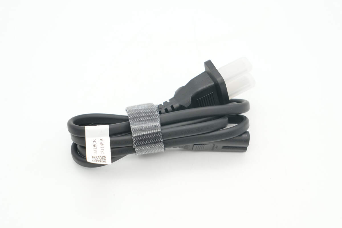
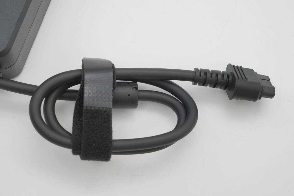
The power cord is neatly bundled with a Velcro strap, and the prongs are covered with a protective plastic cap.
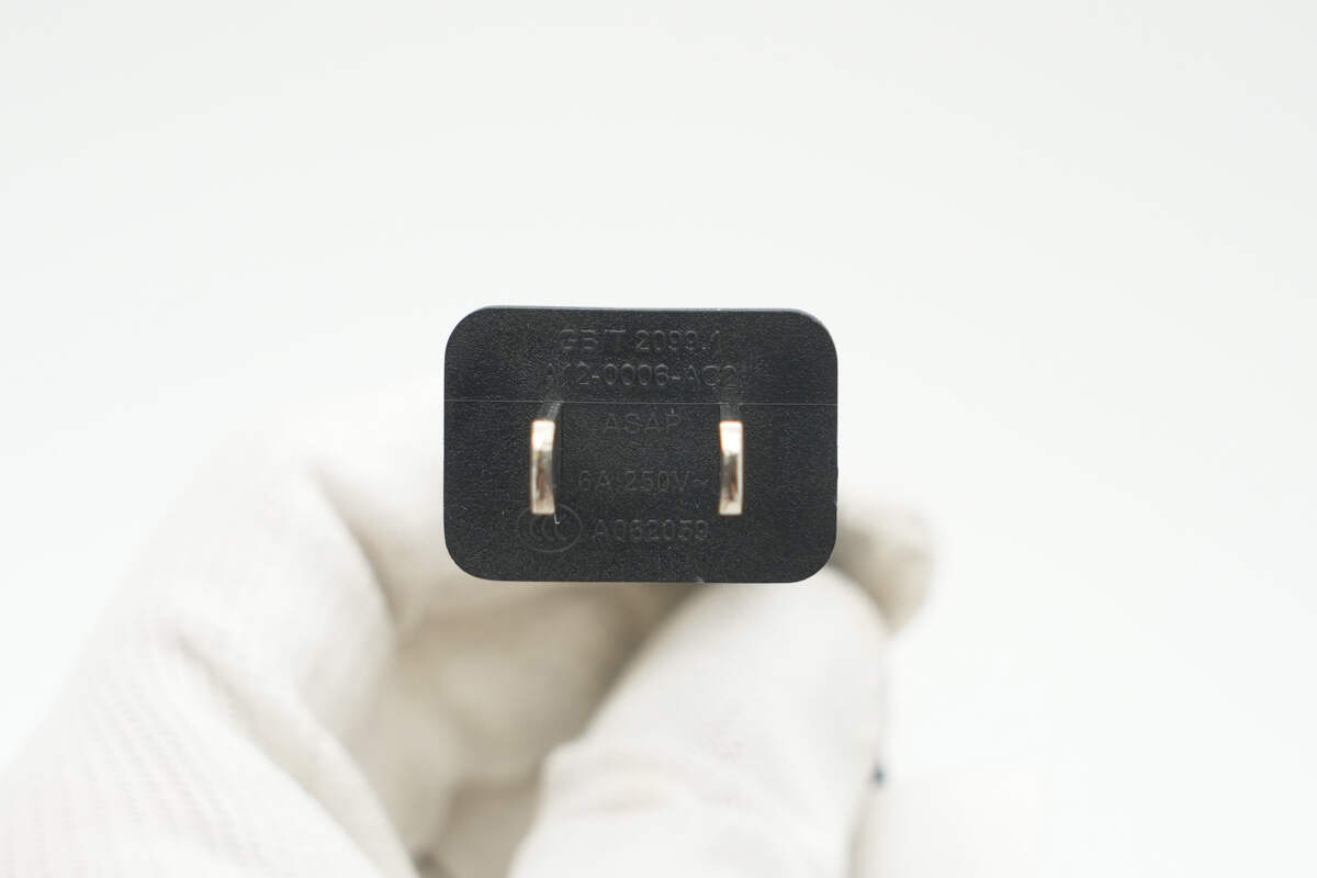
The power cable is rated at 6A 250V and has passed CCC standards.
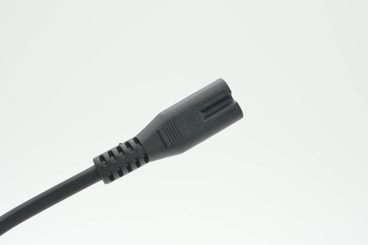
The other end of the cable features a C7 connector.
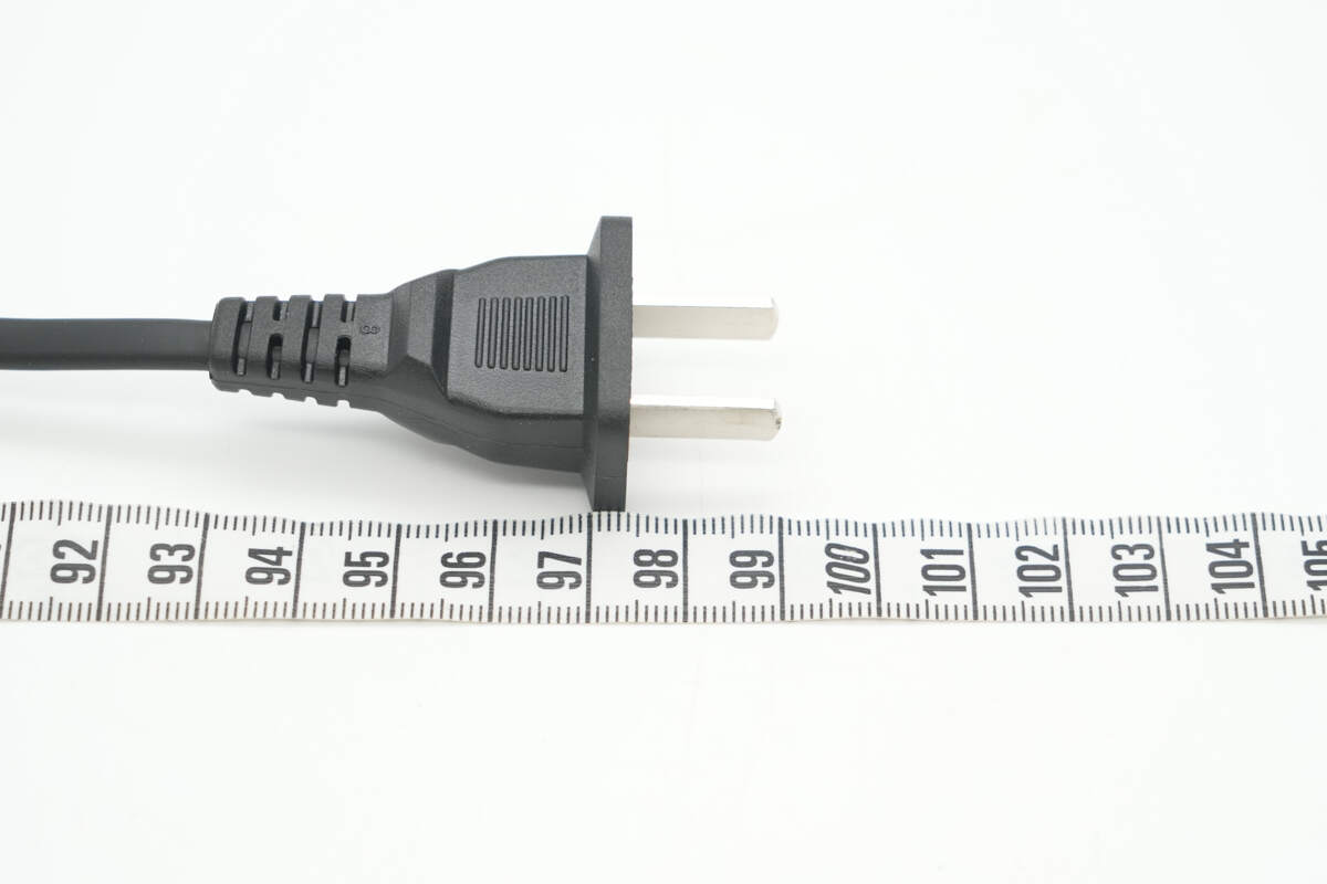
The length is about 1 m (3' 3.37'').
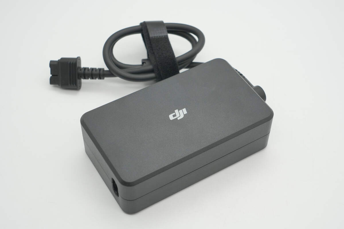
The housing is made of flame-retardant PC with chamfered edges and a matte finish, featuring a minimalist design style.
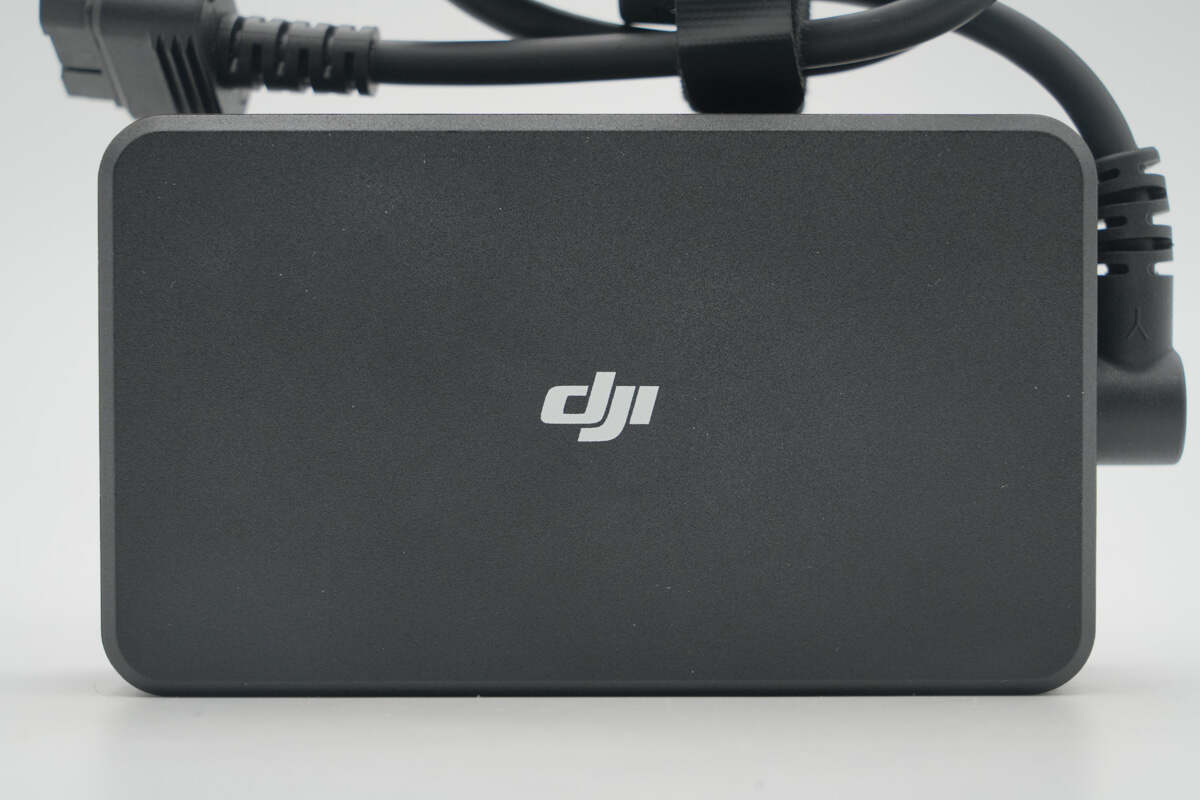
The DJI logo is centered on the top surface.
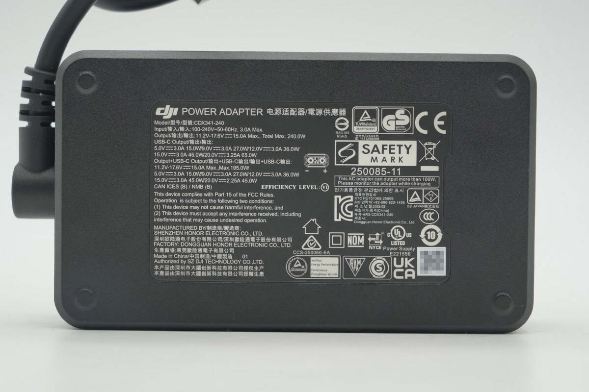
A nameplate with the specifications is affixed to the bottom.
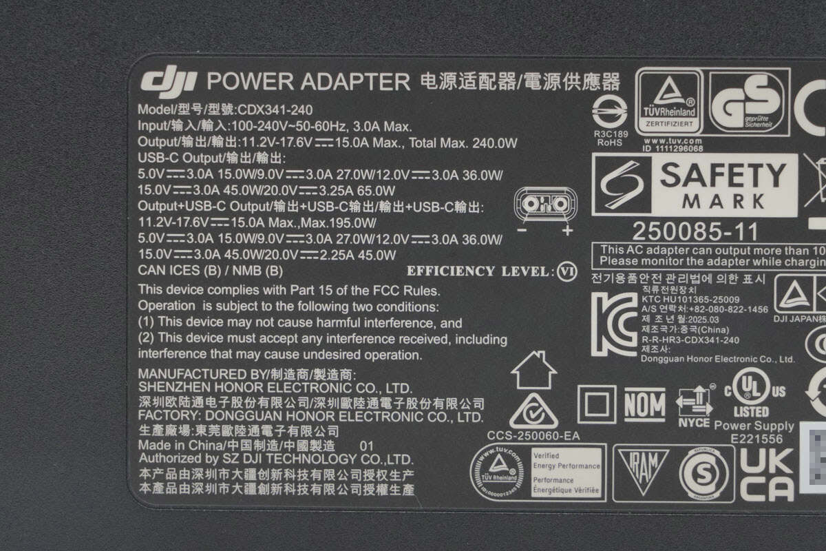
Model: CDX341-240
Input: 100-240V\~ 50-60Hz 3.0A Max
Output: 11.2-17.6V 15A Max, total max 240W
USB-C Output: 5V 3A, 9V 3A, 12V 3A, 15V 3A, 20V 3.25A (65W)
When both outputs are used simultaneously:
Output: 11.2-17.6V 15A Max, up to 195W
USB-C Output: 5V 3A, 9V 3A, 12V 3A, 15V 3A, 20V 2.25A (65W)
The product is certified by CCC, CE, PSE, GS, KC, NOM, NYCE, UL, and UKCA.
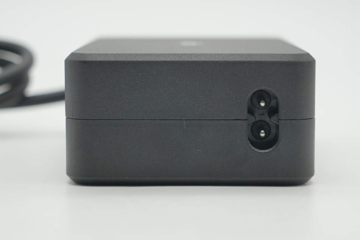
The input end uses a C7 socket.
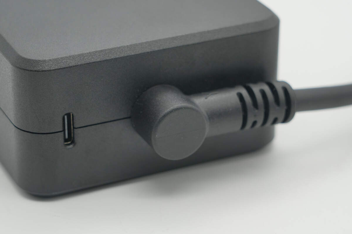
The integrated output cable features reinforced protection and an anti-bending design.
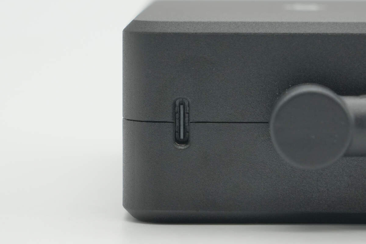
There is also a USB-C port.
The output cable is bundled with a Velcro strap and features an anti-interference ferrite bead.
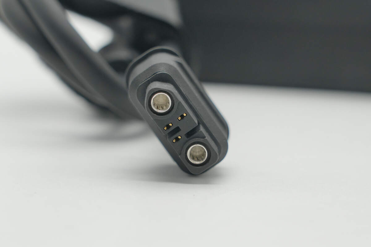
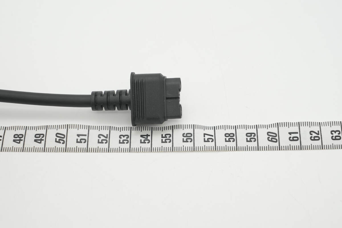
The output cable’s Mini SDC connector is designed with reverse insertion protection.
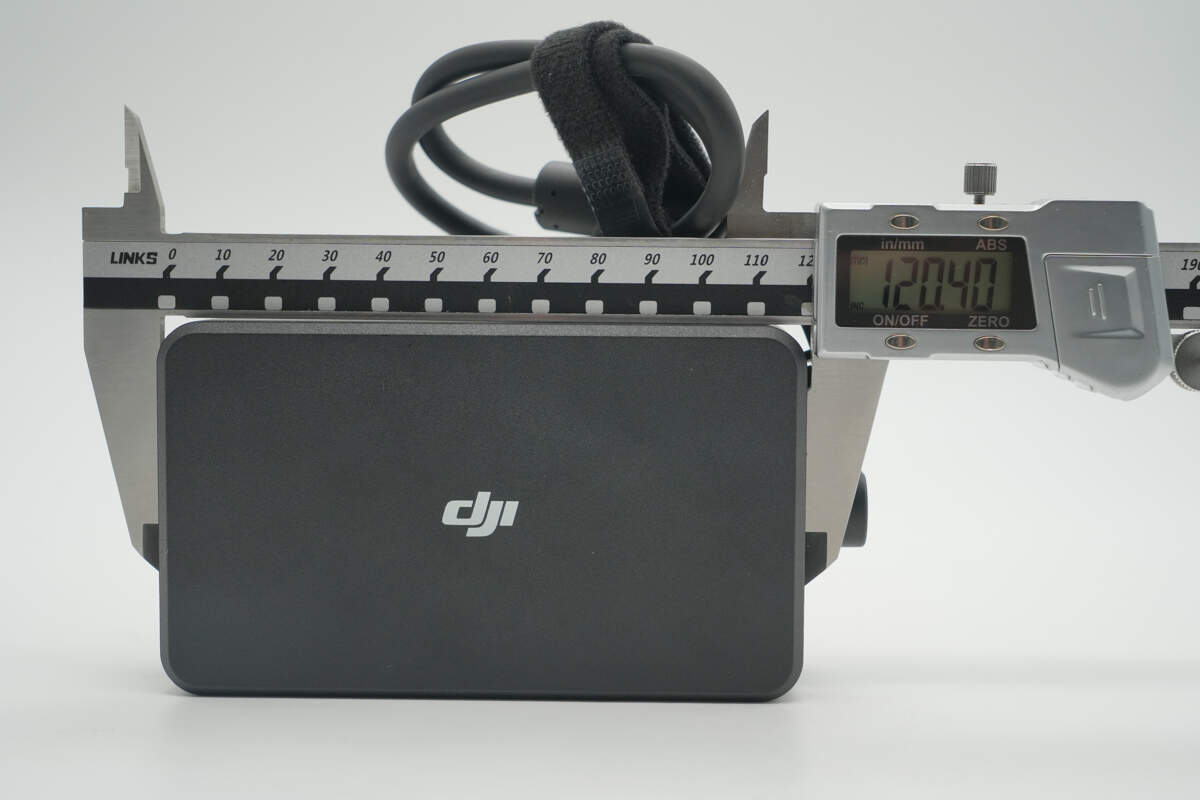
The length of the adapter is about 120.4 mm (4.74 inches).
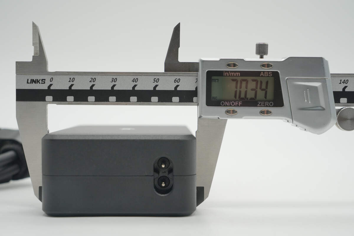
The width is about 70.34 mm (2.77 inches).
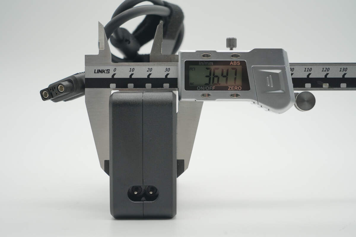
The thickness is about 36.47 mm (1.44 inches).
The length of the output cable is about 55.5 cm (21.85 inches).
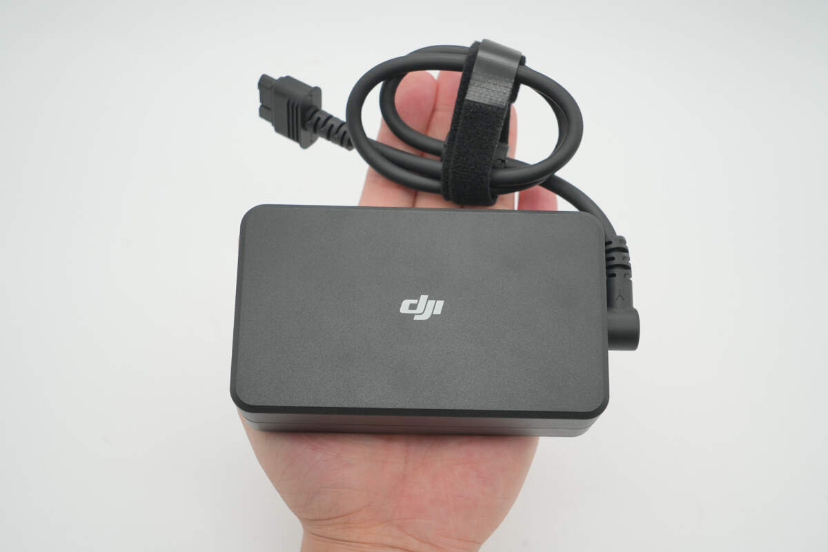
That's how big it is in the hand.
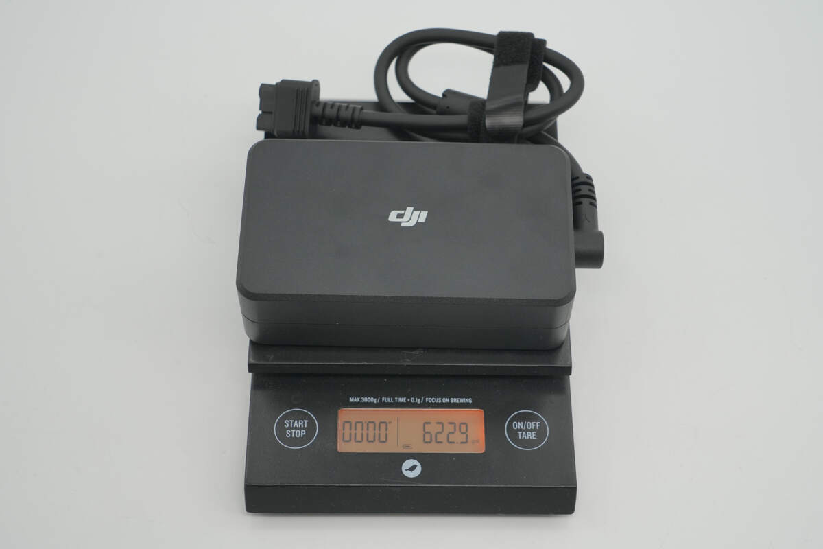
The weight is about 623 g (21.98 oz).
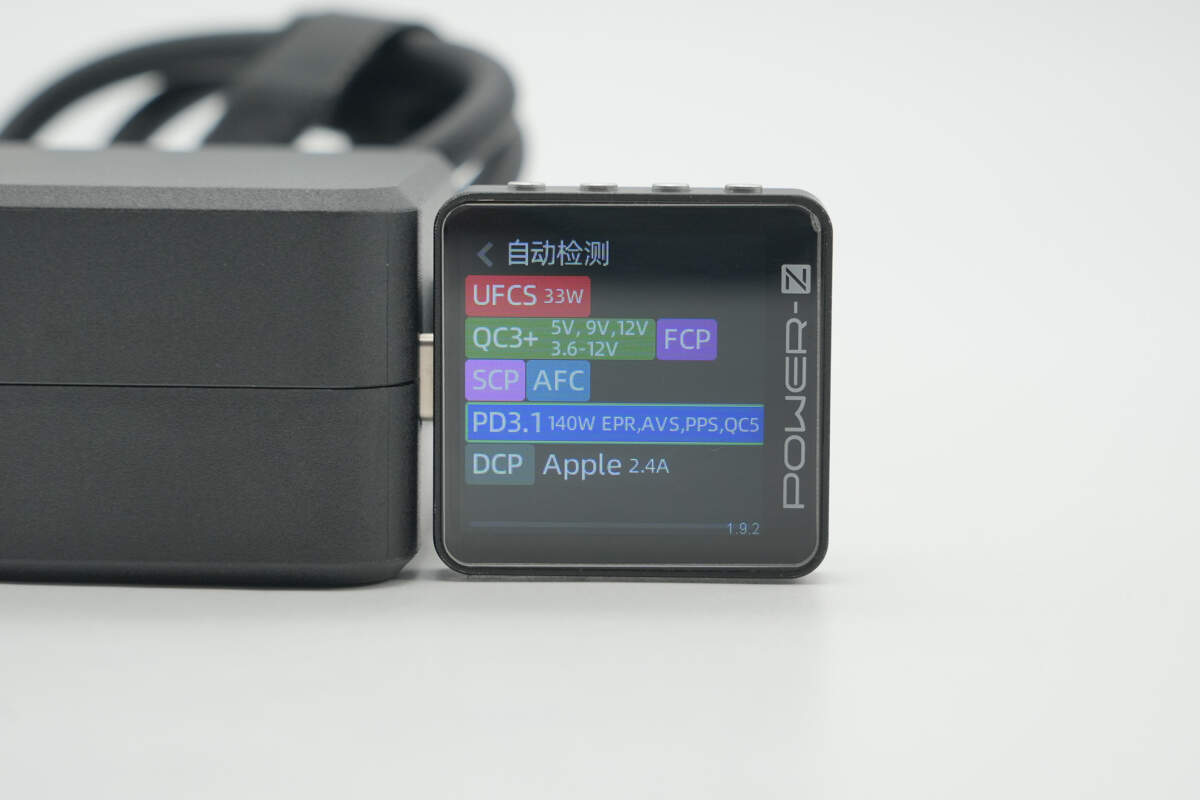
ChargerLAB POWER-Z KM003C shows that the USB-C supports UFCS, QC3+/5, FCP, SCP, AFC, PD3.1, PPS, DCP, and Apple 2.4A protocols.
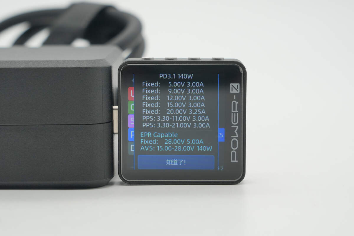
It supports six fixed PDOs of 5V3A, 9V3A, 12V3A, 15V3A, 20V3.25A, and 28V5A. It also has two sets of PPS, which are 3.3-11V3A and 3.3-21V3A.
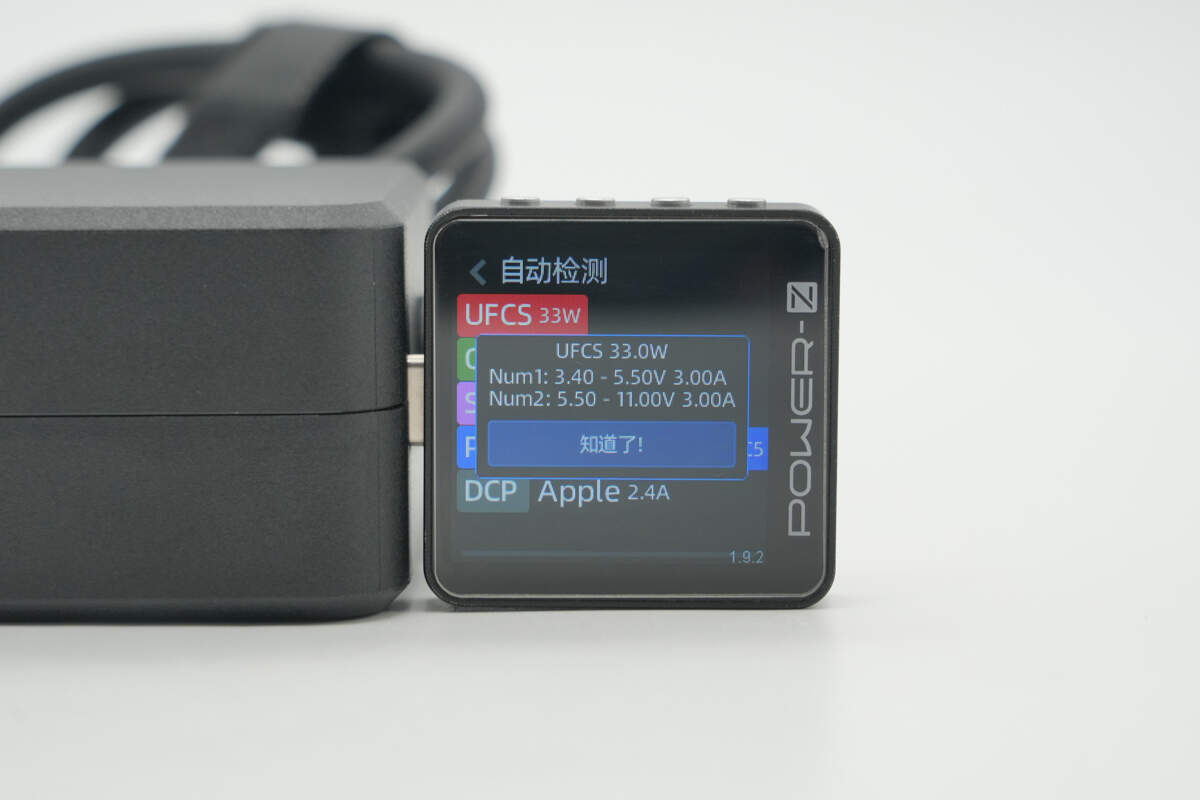
Testing shows that the UFCS universal fast charging supports two voltage ranges: 3.4–5.5V at 3A and 5.5–11V at 3A.
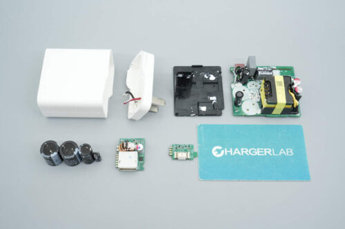
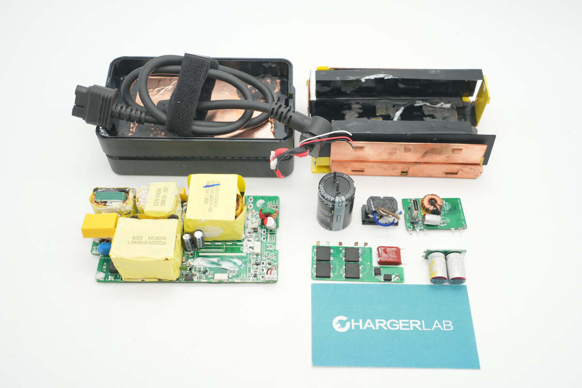
Teardown
Next, let's take it apart to see its internal components and structure.
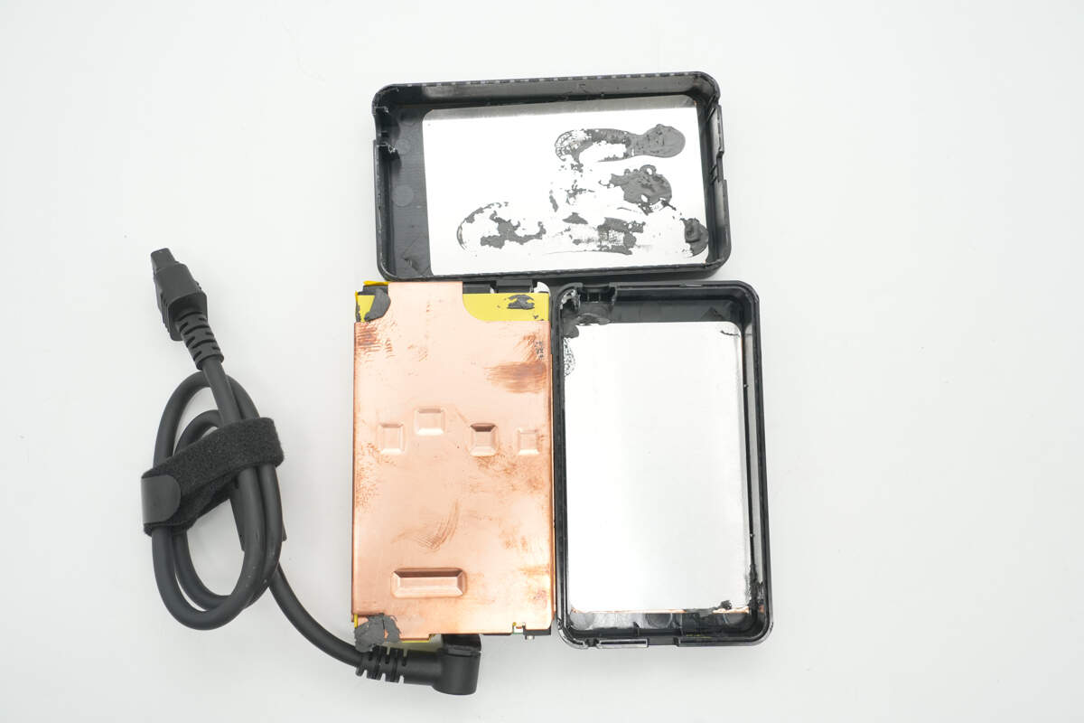
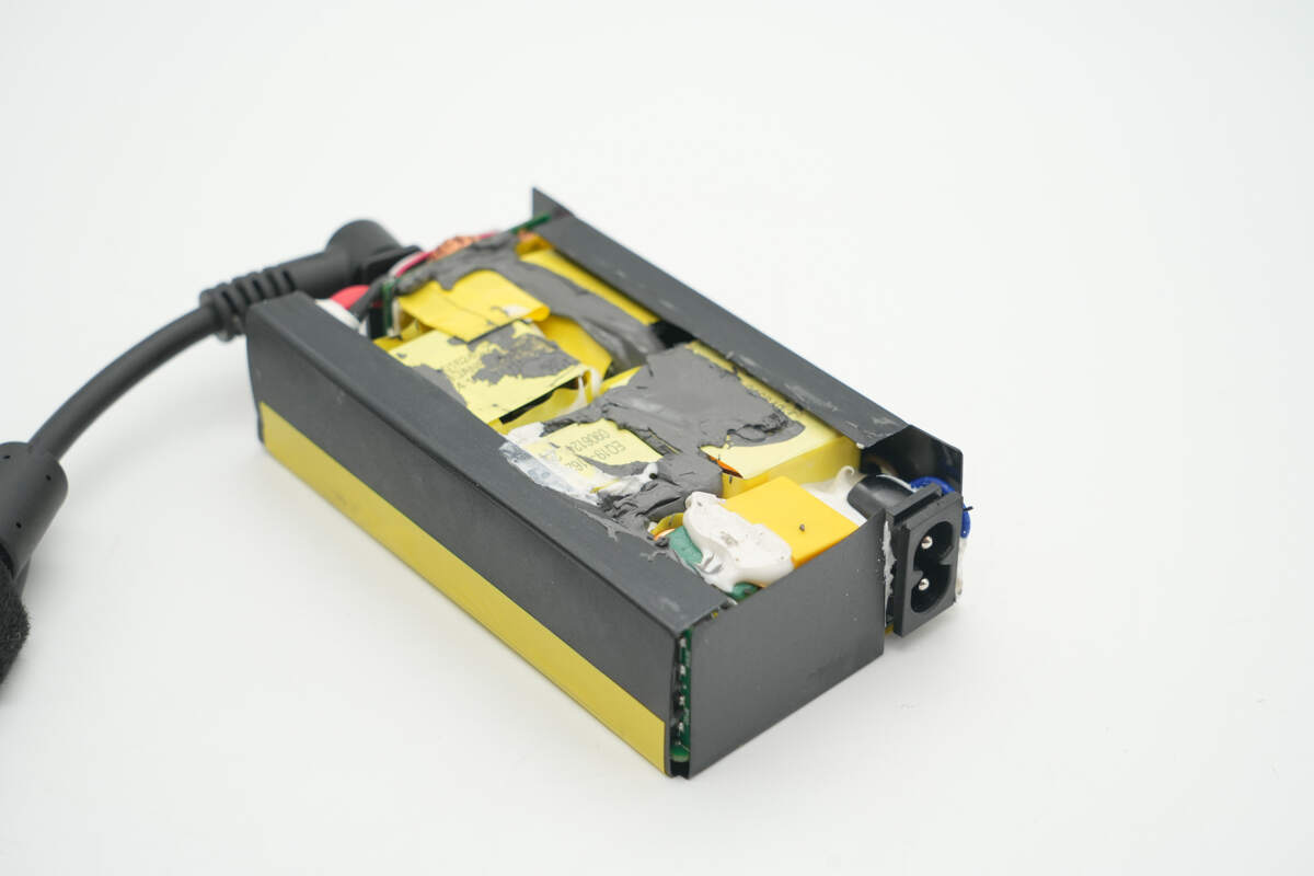
After disassembling the power adapter, it was found that the casing is joined using ultrasonic welding.
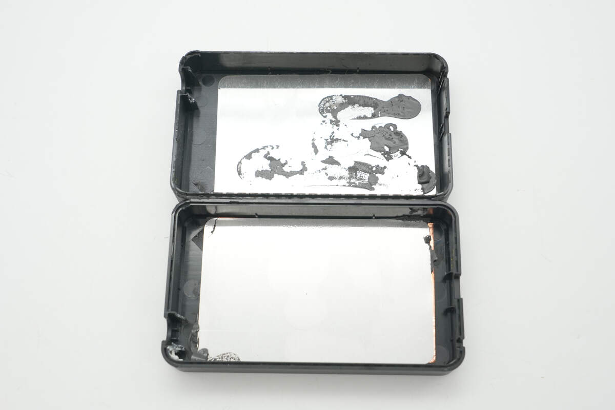
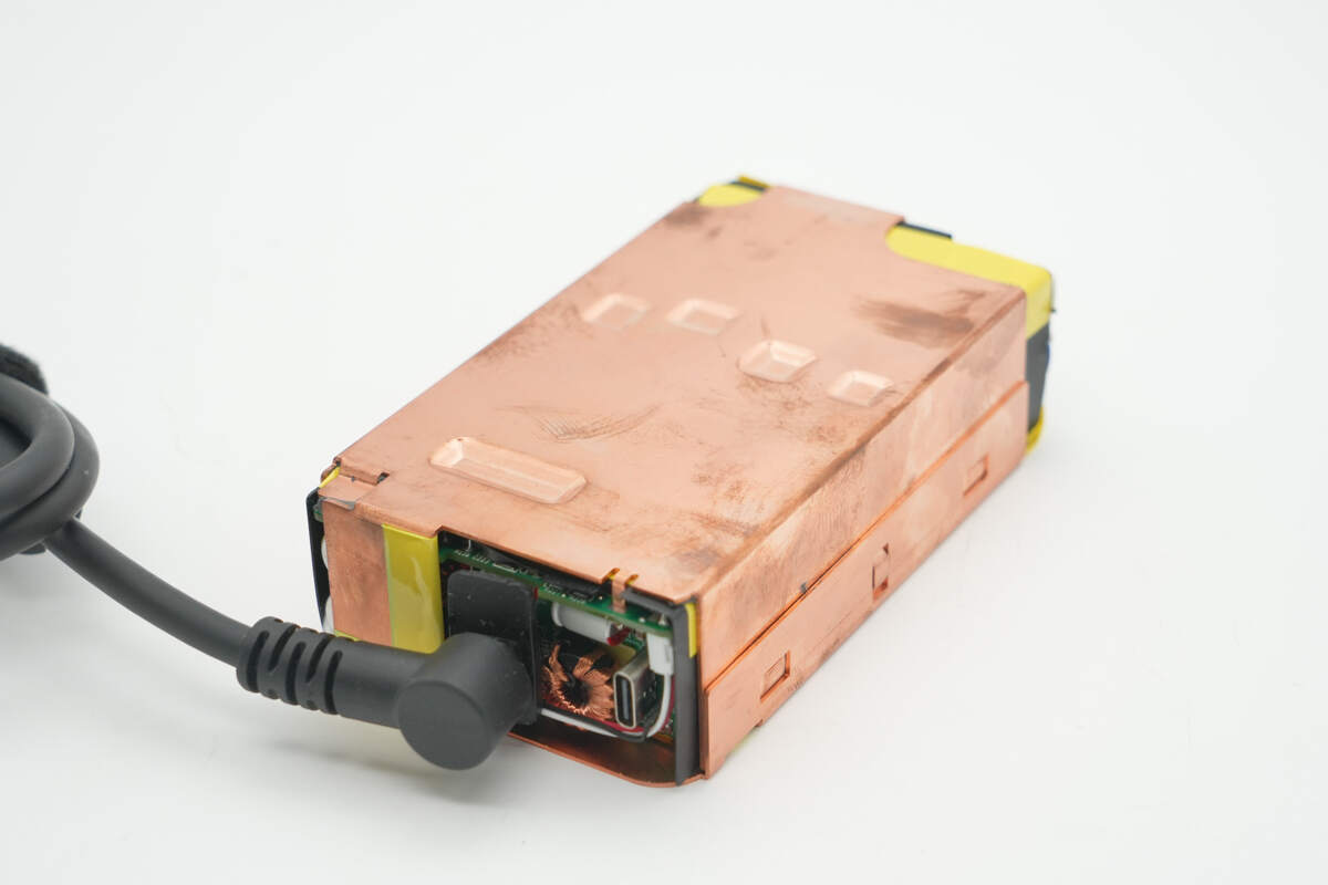
Both parts of the casing are equipped with metal heat dissipation plates.

Copper foils are also embedded within the heat sinks.
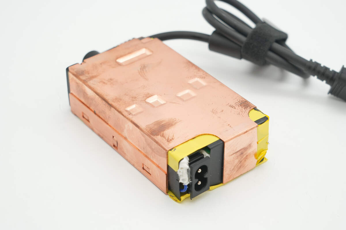
The entire PCBA module is covered with copper heat sinks.
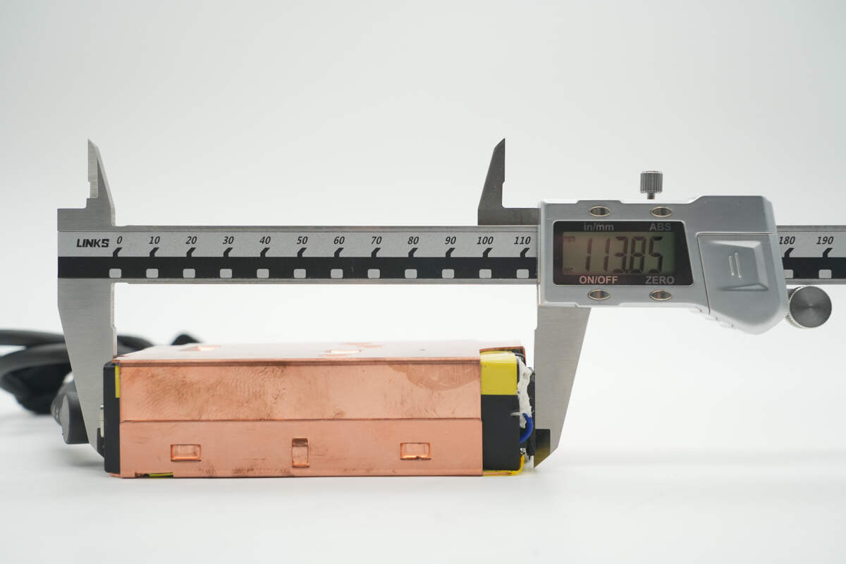
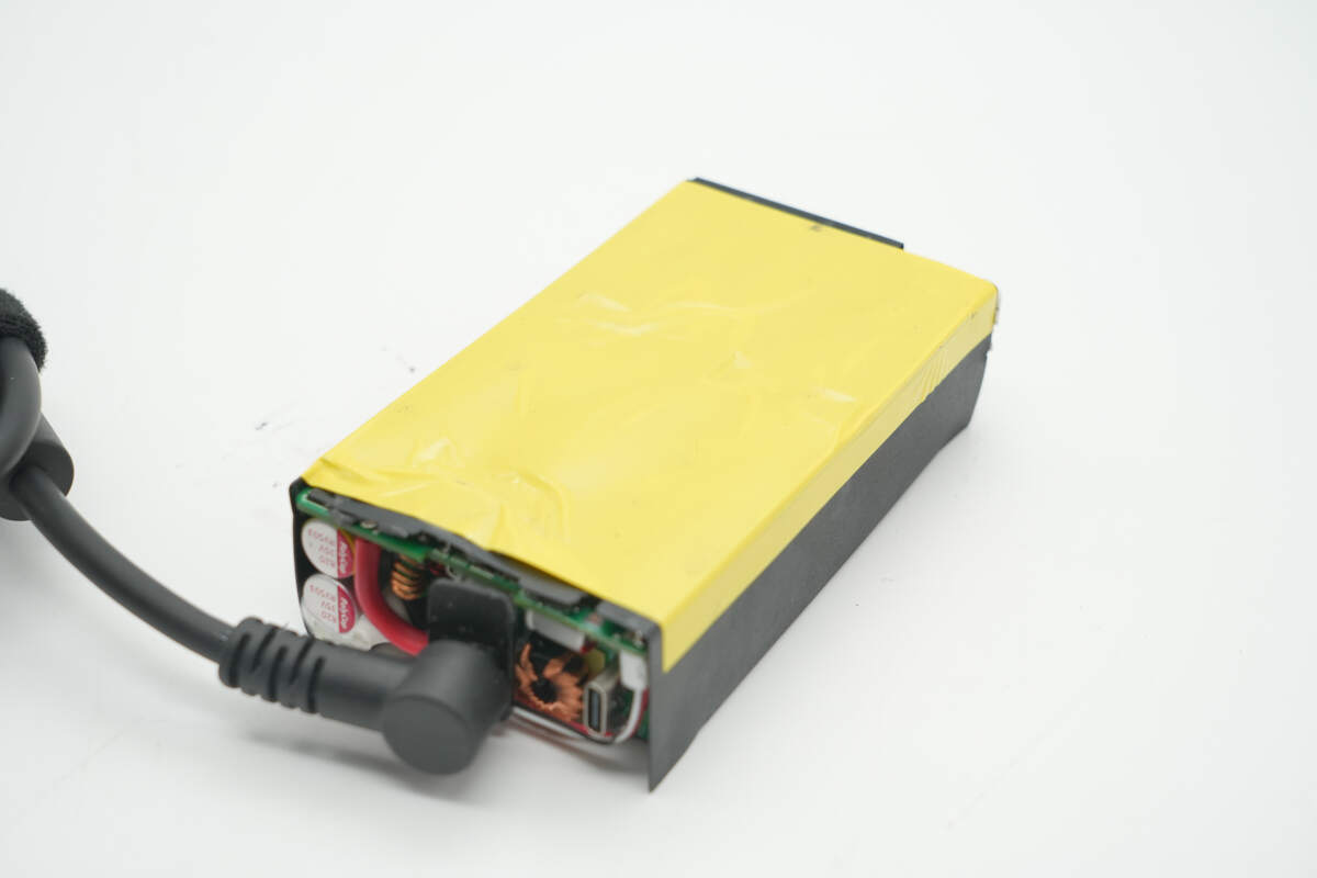
The length of the PCBA module is about 113.85 mm (4.48 inches).
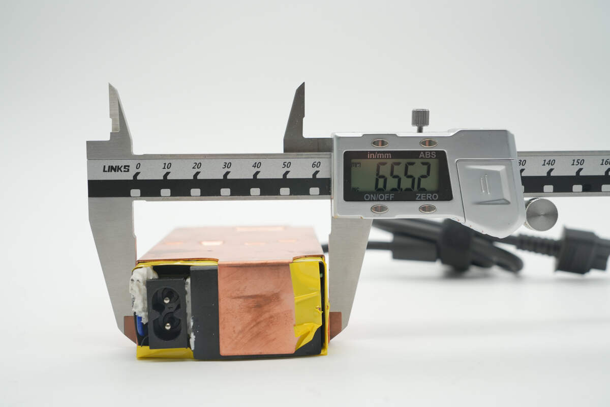
The width is about 65.52 mm (2.58 inches).
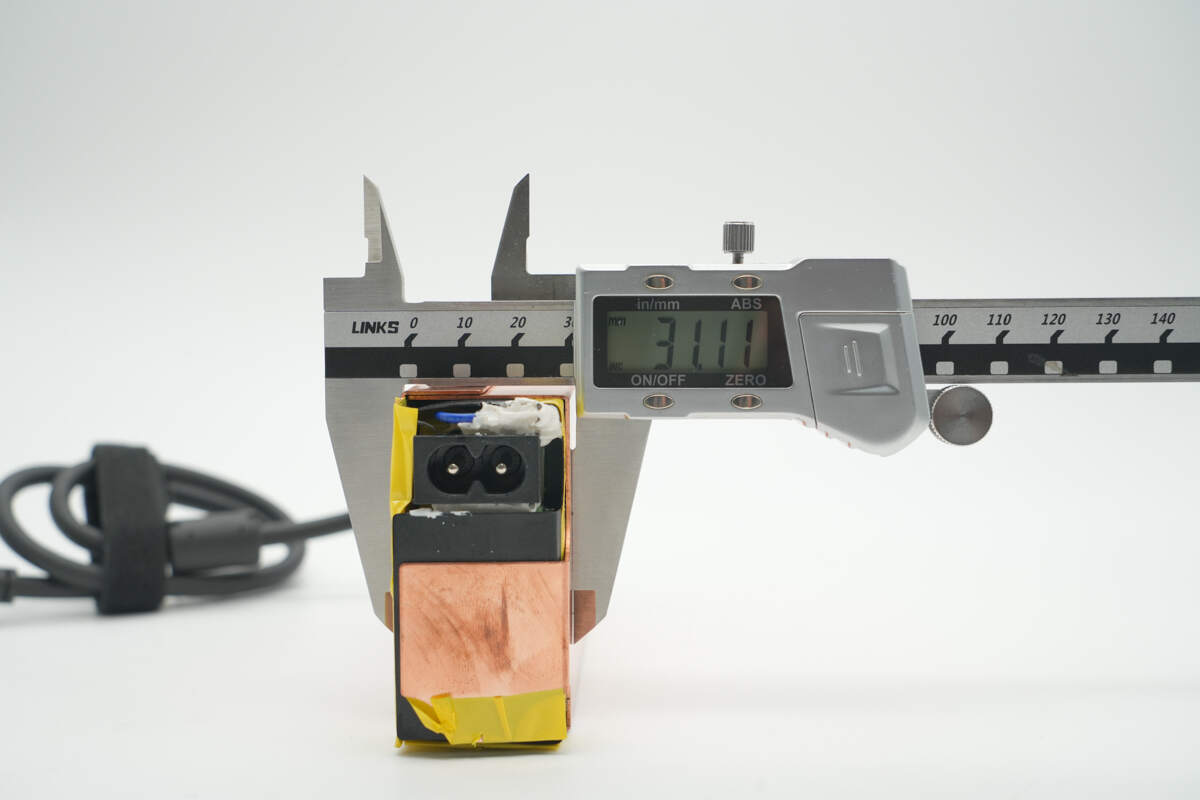
The thickness is about 31.11 mm (1.22 inches).
The copper heat sink is fixed with snap-fits.
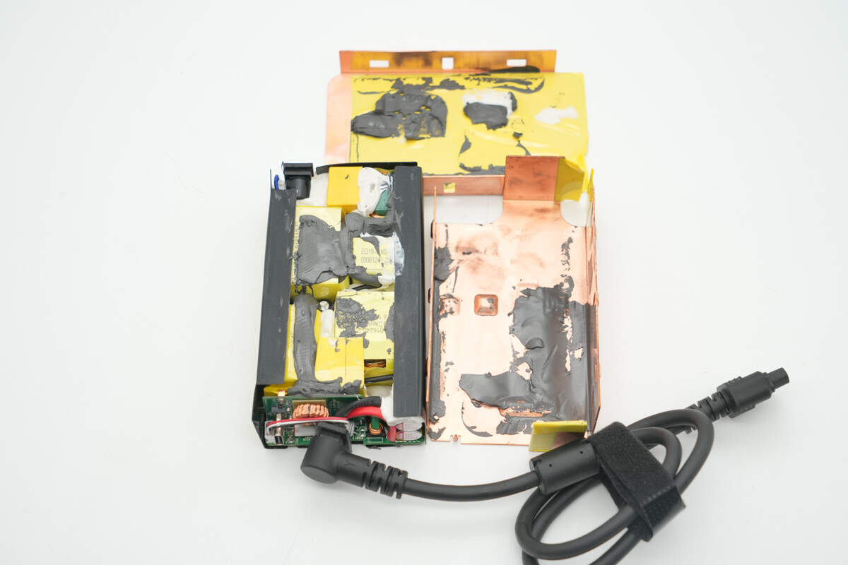
After removing the heat sink, we found that the inside was filled with thermal conductive glue.
The bottom, both sides, and the output end of the PCBA module are wrapped with Mylar sheets for isolation.
A yellow insulating tape is applied on the Mylar sheet.
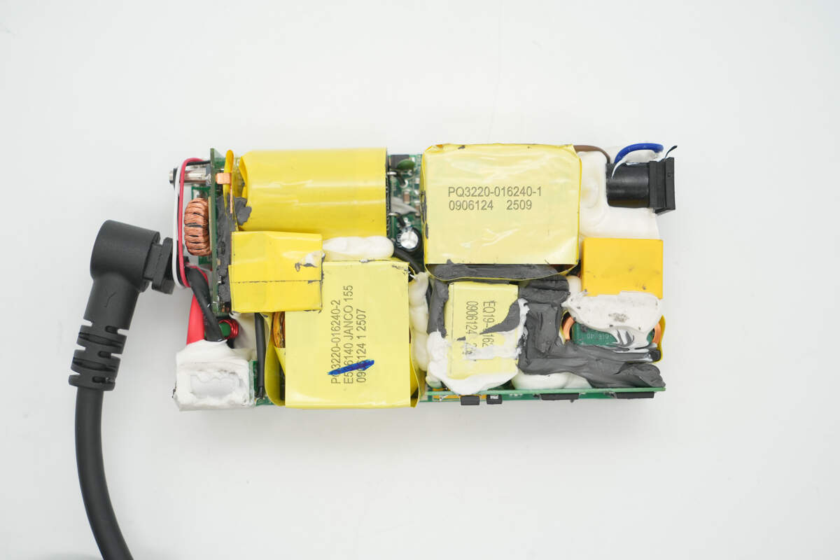
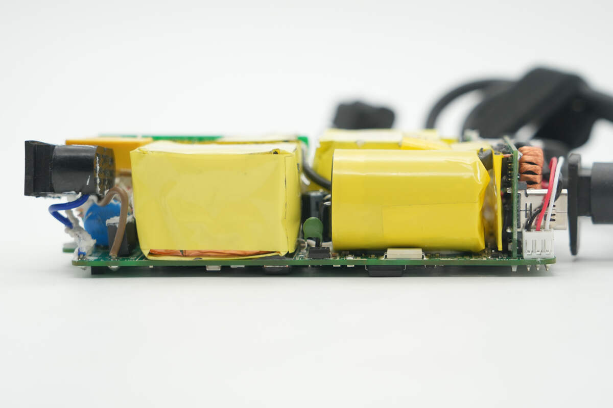
The components on the front side of the PCBA module are arranged compactly and orderly, with gaps filled and reinforced with potting compound.
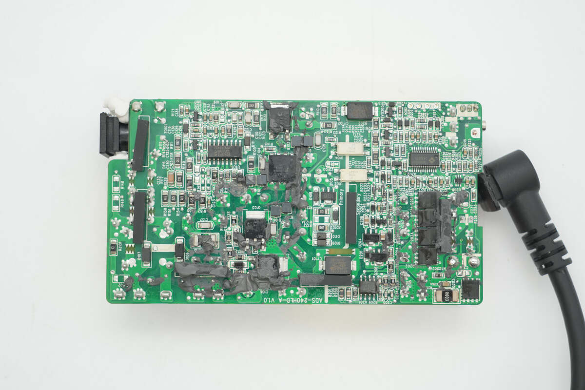
Thermal compound is applied on the back of the mainboard in the area corresponding to the core power devices to aid heat dissipation.
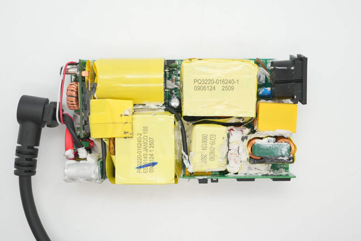
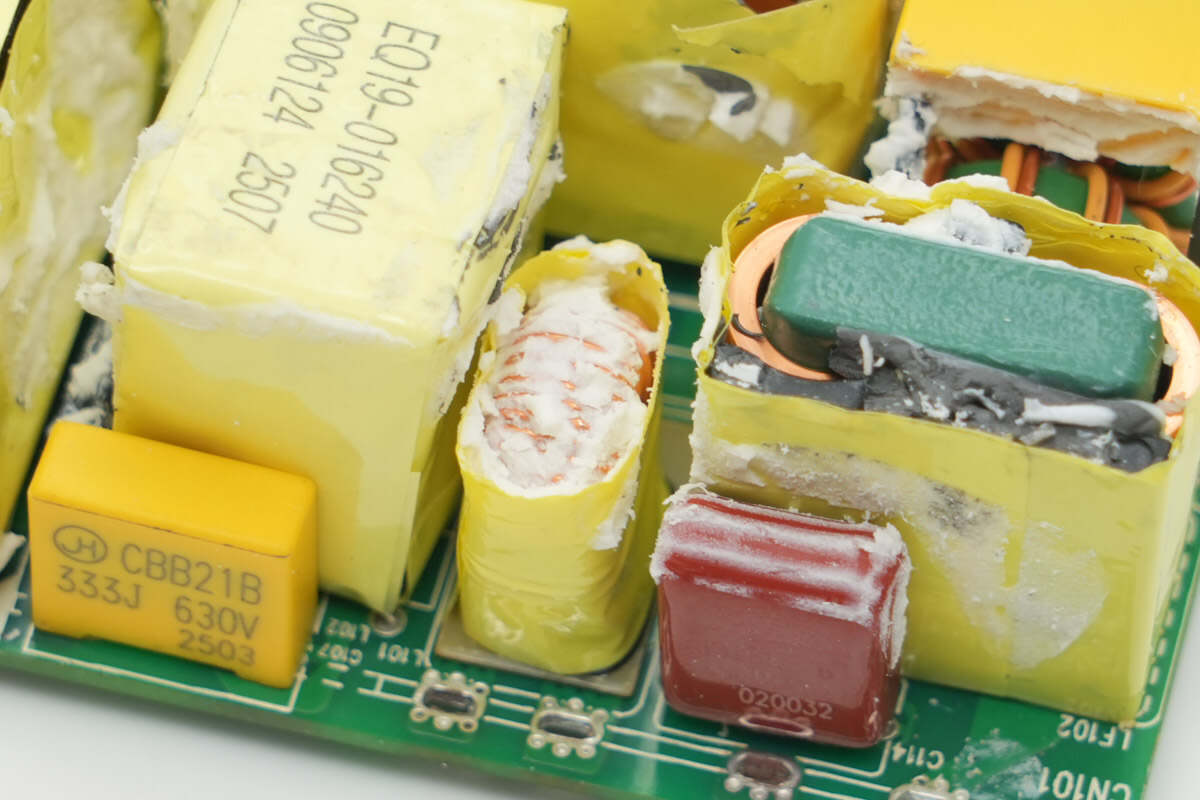
The front side of the mainboard is equipped with components such as a time-delay fuse, common mode choke, PFC boost inductor, electrolytic capacitor, and transformer. Additionally, small PCBs are soldered on the sides and at the output end.
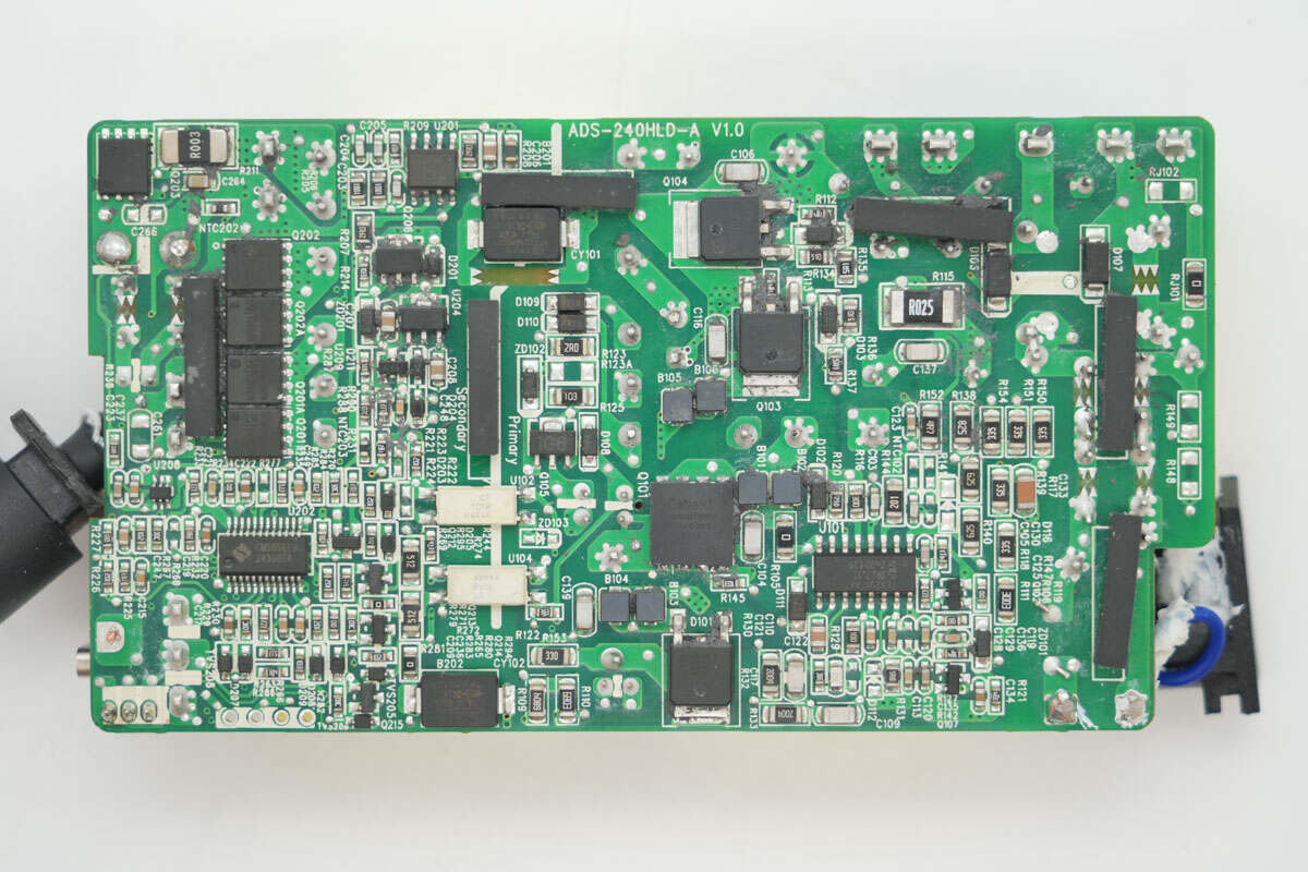
The back features components such as the master control chip, PFC MOSFET, PFC rectifier, LLC MOSFET, synchronous rectifier controller, and synchronous rectifier. Multiple thermal pads are also attached for support.
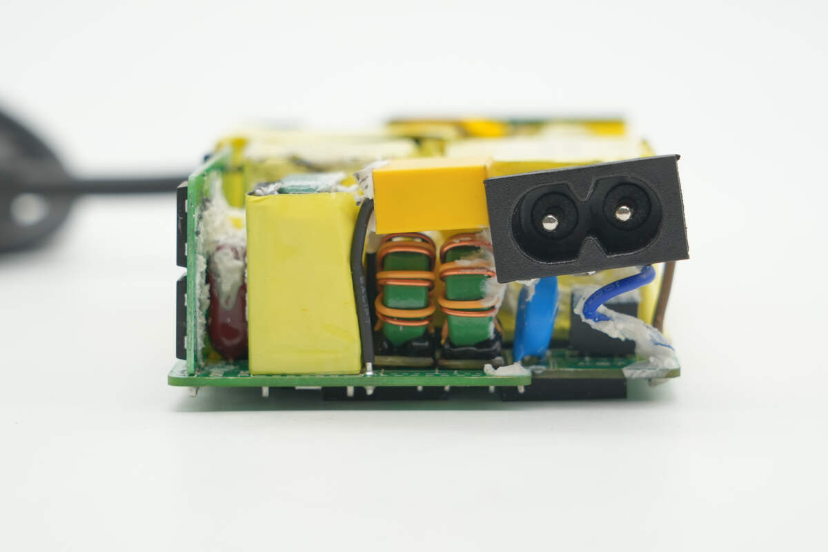
At the input end of the PCBA module, the socket connector is connected to the mainboard via wires. Components such as a time-delay fuse, varistor, common mode choke, and safety X2 capacitor are also present.
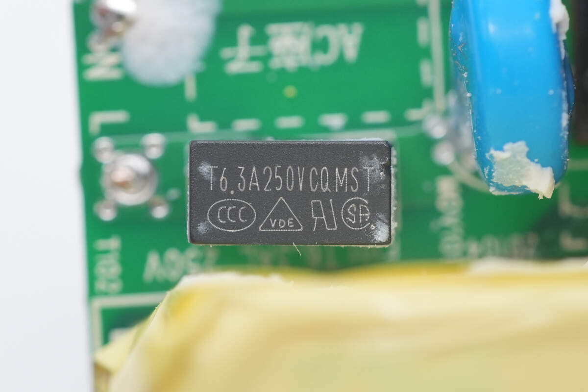
Close-up of the time-delay fuse. 6.3A 250V.
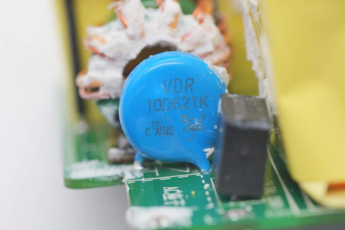
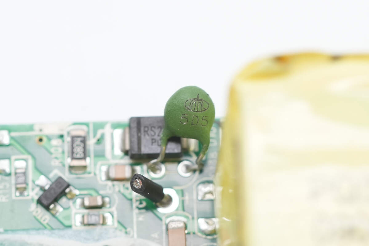
The 10D621K varistor is used for input overvoltage protection.
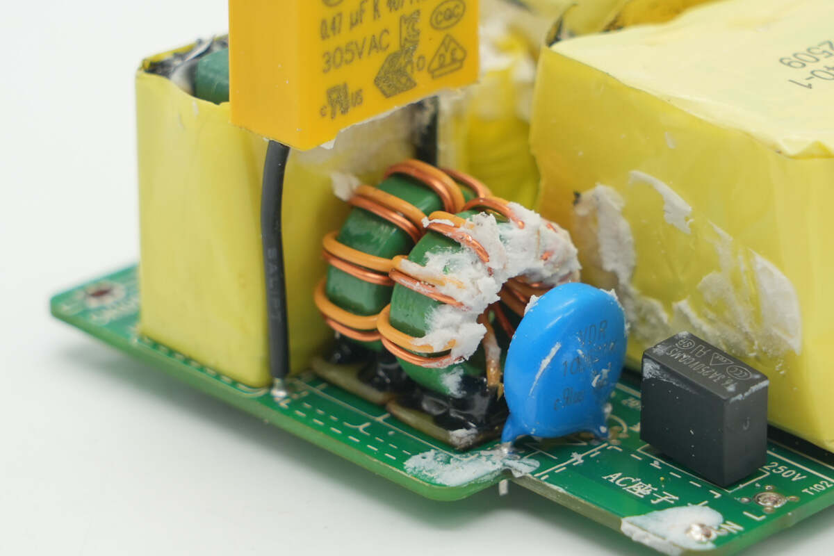
The common mode choke adopts a three-stage design to filter out EMI interference. It consists of two dual-wound coils and is insulated with bakelite.
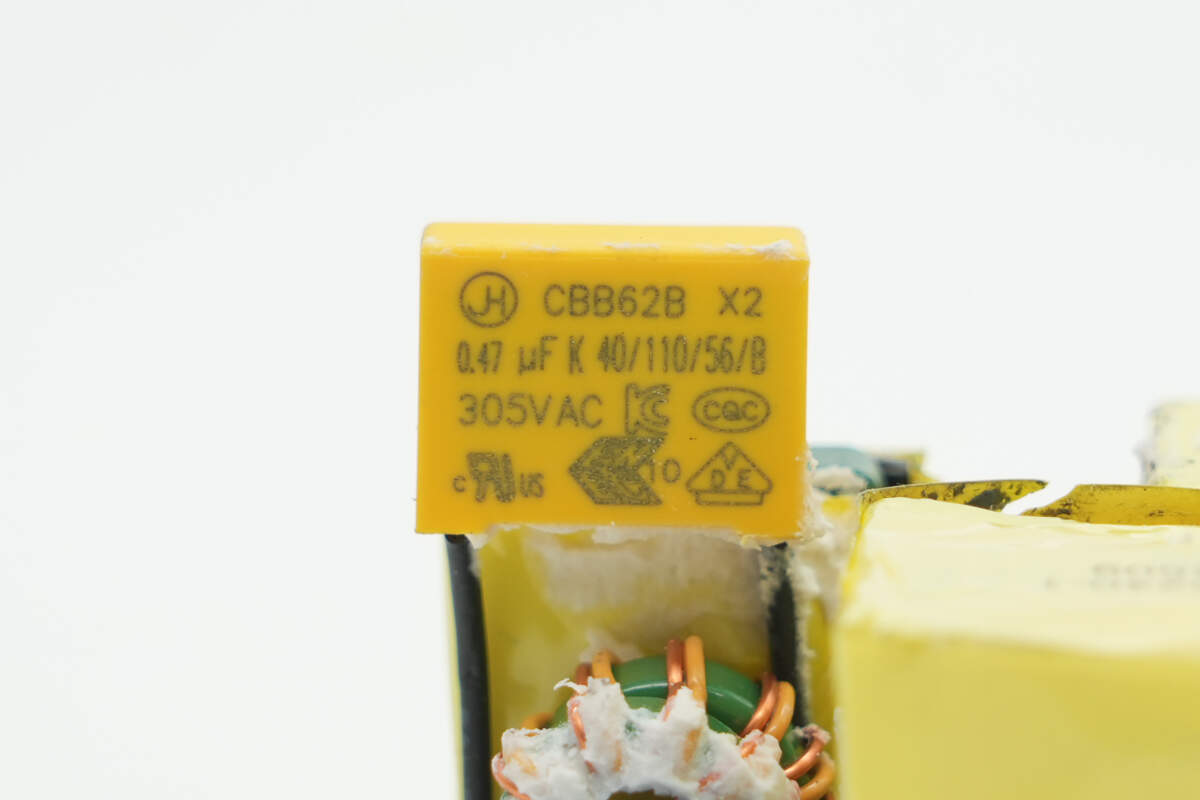
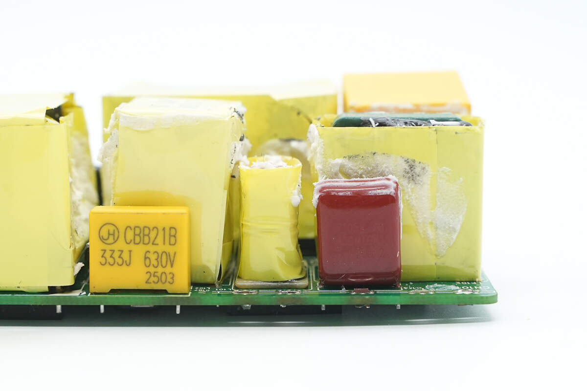
The safety X2 capacitor is from JH. 0.47μF.
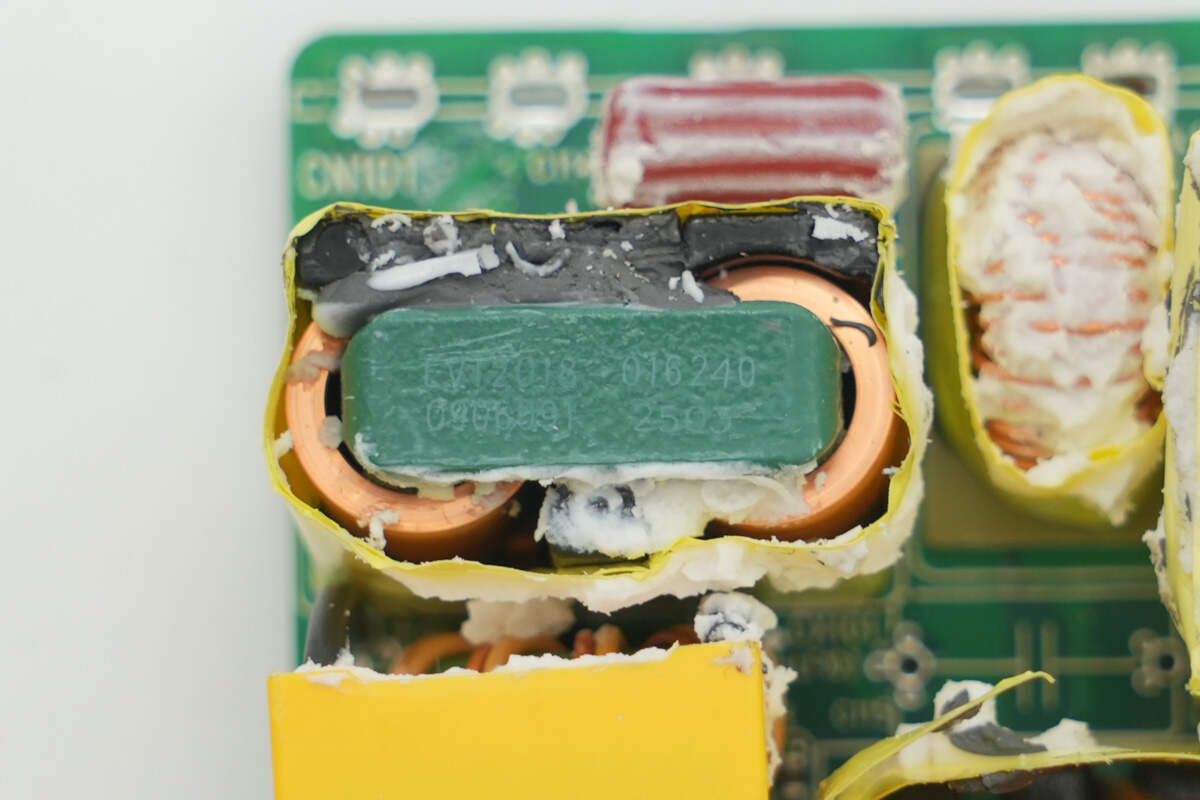
The third common mode choke is wound with flat copper strips and wrapped with insulating tape.
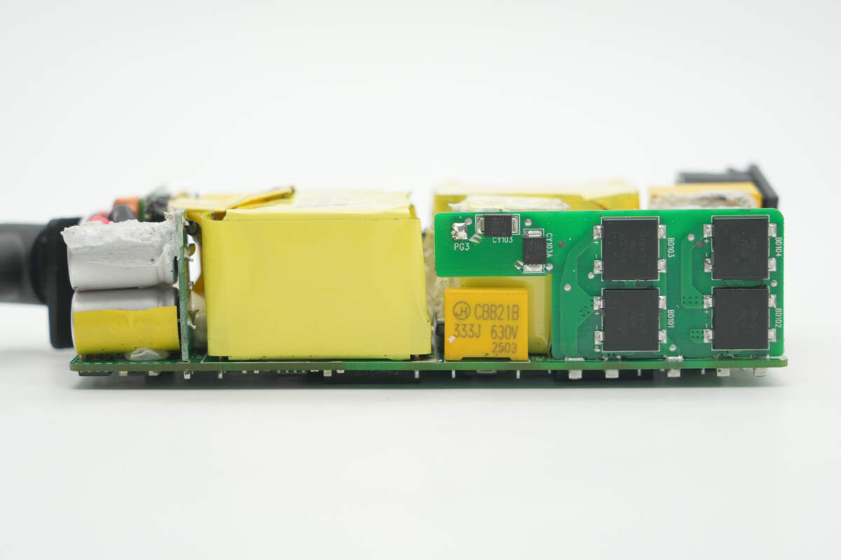
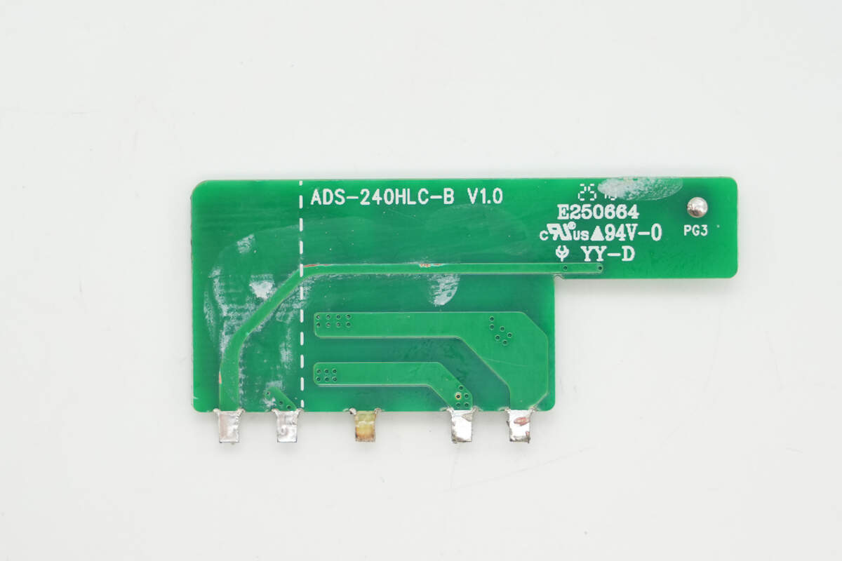
One side of the module is soldered with a rectifier PCB, resonant inductor, resonant capacitor, transformer, and solid capacitors for output filtering.
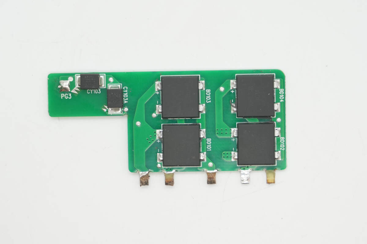
After removing the rectifier PCB, the front side reveals four bridge rectifiers and two SMD Y capacitors.
There are no components on the back.
In the area covered by the small PCB, there are a film capacitor, a filter inductor, a resonant capacitor, and a resonant inductor.
On the other side, there is a PFC boost inductor and an electrolytic capacitor.
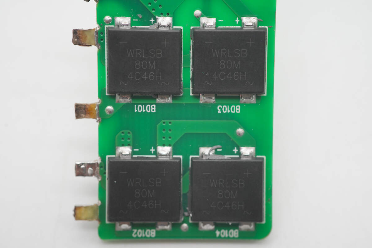
The four bridge rectifiers are from World Industrial, model WRLSB80M. This soft recovery bridge has a gentle recovery curve and smooth turn-off characteristics, reducing diode junction capacitance and minimizing harmonic oscillations. The LSB package provides excellent thermal dissipation, improving reliability for medium to high-wattage adapters. Each unit supports over 60W.
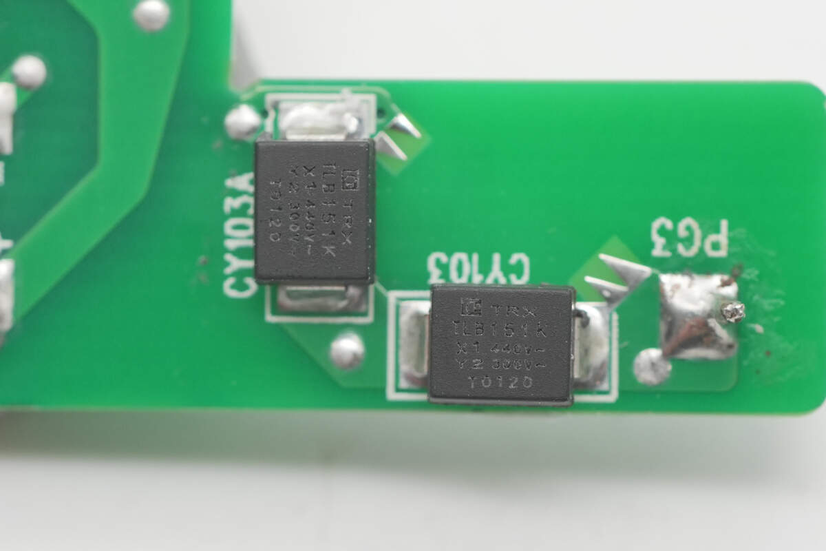
Two SMD Y capacitors are from TRX, model number TBY2151KB.
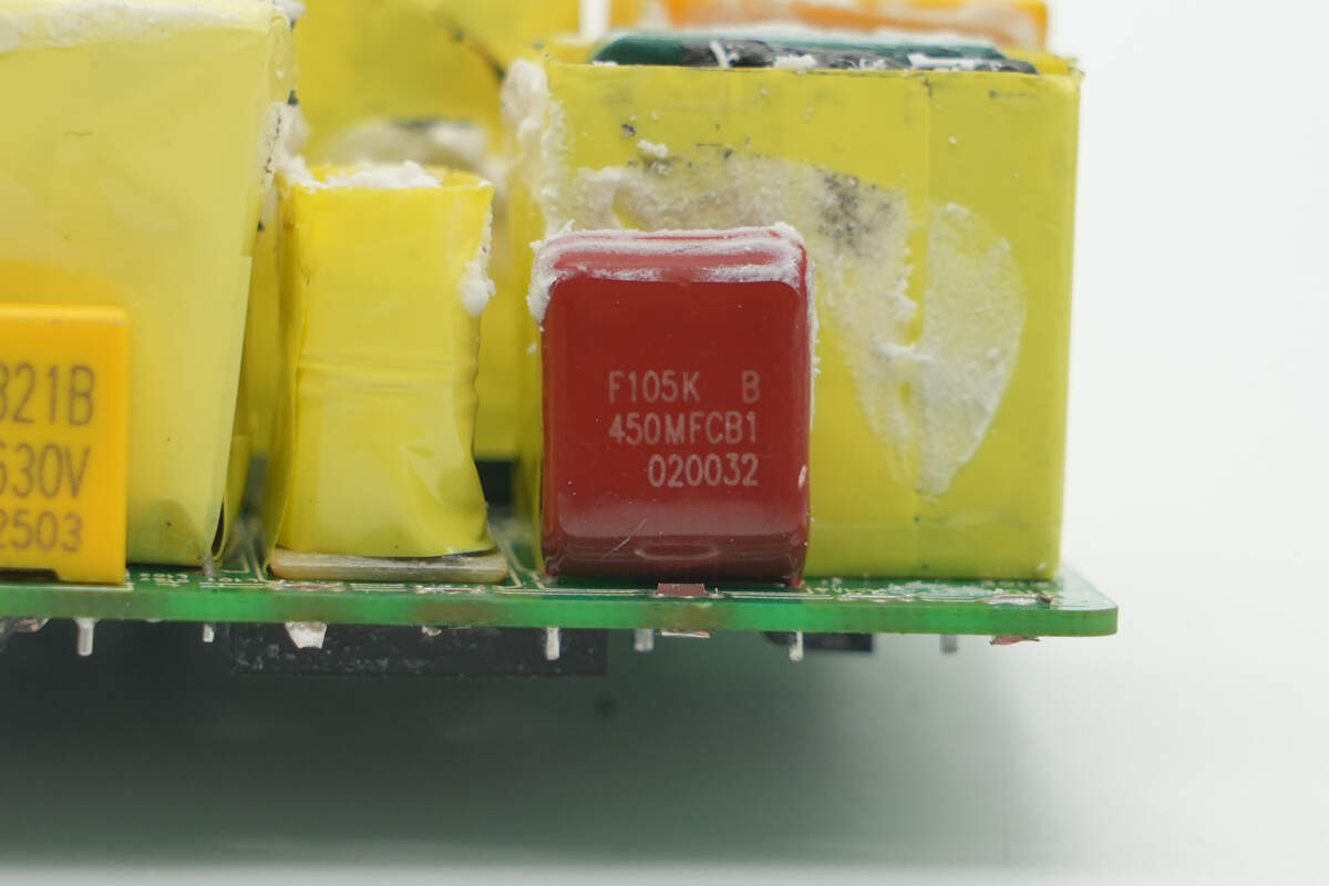
Close-up of the film capacitor. 1μF 450V.
The filter inductor is wrapped with insulating tape.
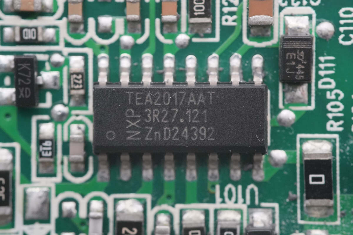
The master control chip is from NXP, model TEA2017AAT. It is a digitally configurable combined LLC and PFC controller designed for high-efficiency resonant power supplies. The chip integrates both LLC and PFC controller functions. The PFC can be configured to operate in DCM/QR, CCM fixed frequency, or a multi-mode supporting all operating modes, optimizing PFC efficiency.
The chip features built-in high-voltage startup and X-capacitor discharge functions. It also includes an internal driver capable of directly driving the high-voltage upper MOSFET without the need for an external driver. The PFC supports three configurable operation modes: DCM/QR, a hybrid mode combining DCM/QR/CCM, and CCM fixed frequency, catering to different power application requirements.
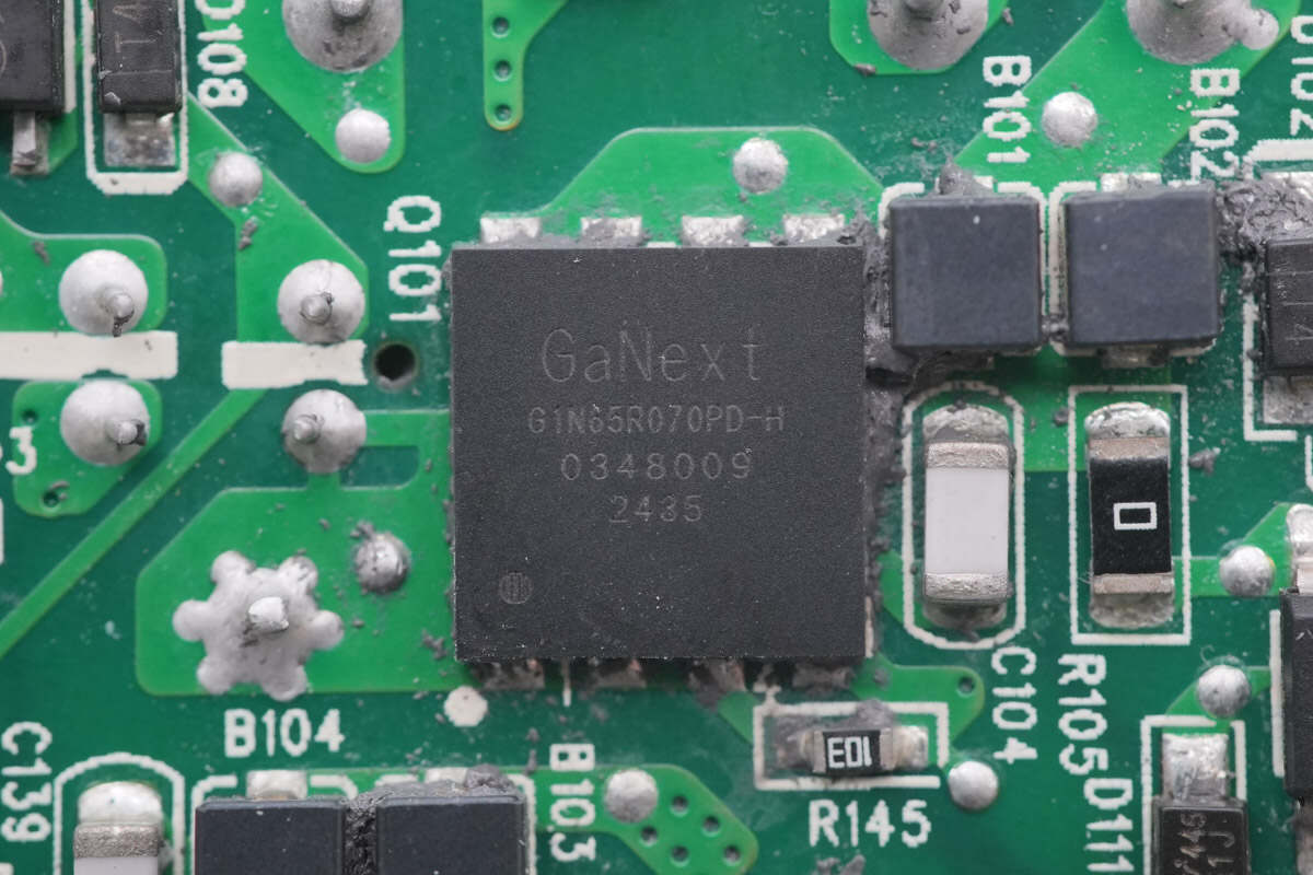
The PFC MOSFET used is the GaNext G1N65R070PD-H, a 650V-rated GaN power device with a transient voltage tolerance of 800V. It features a nominal on-resistance of 70mΩ and a gate voltage rating of ±20V, allowing it to be driven by traditional silicon MOSFET drivers. Compared to enhancement-mode GaN devices, it significantly simplifies the gate driver circuit design.
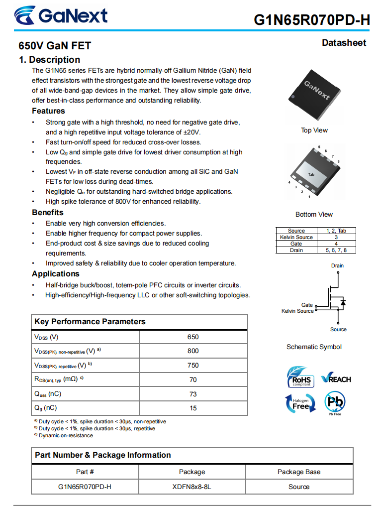
The GaNext G1N65R070PD-H uses an XDFN8x8-8L package, with the source as the thermal pad. This design reduces the high-frequency trace area and improves EMI performance.
Close-up of the PFC boost inductor.
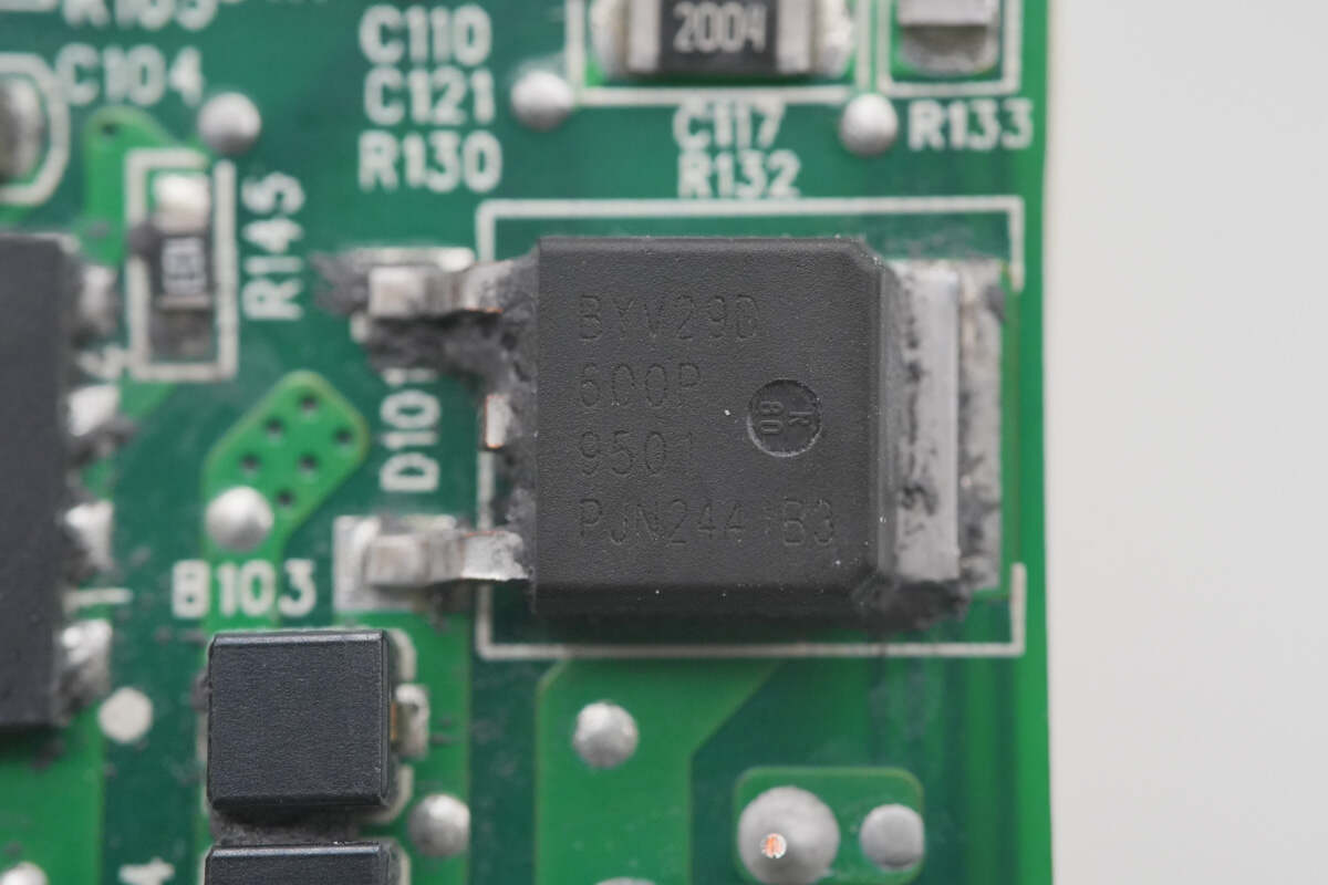
The PFC rectifier is from RePower, model BYV29D-600P. It is an ultra-fast recovery diode rated at 600V and 9A, housed in a TO-252 package.
The NTC thermistor is from Shiheng and is used to suppress inrush current during capacitor charging.
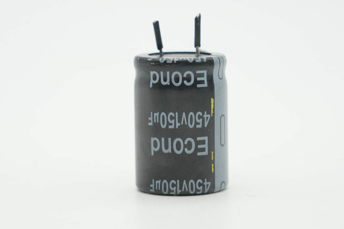
The high-voltage filter capacitor is from Econd. 450V 150μF.
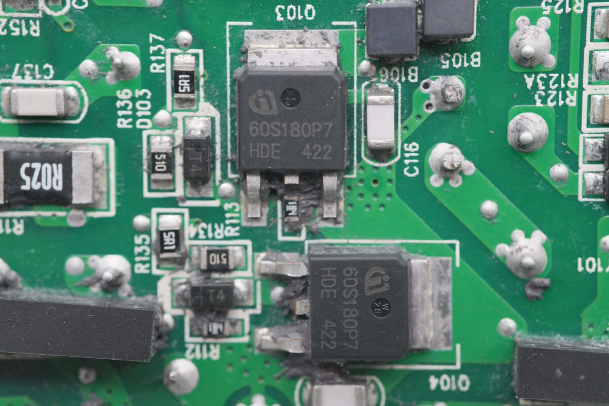
The LLC MOSFET is from Infineon, marked 60S180P7, model IPD60R180P7S. It belongs to the CoolMOS P7 series, with a voltage rating of 650V and an on-resistance of 180mΩ. It comes in a TO-252-3 package.
Close-up of the resonant inductor.
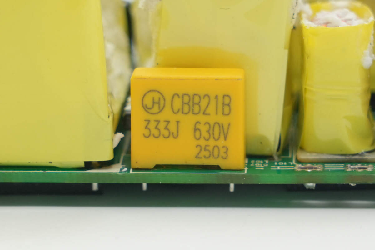
The resonant capacitor is also from JH. 0.033μF 630V.
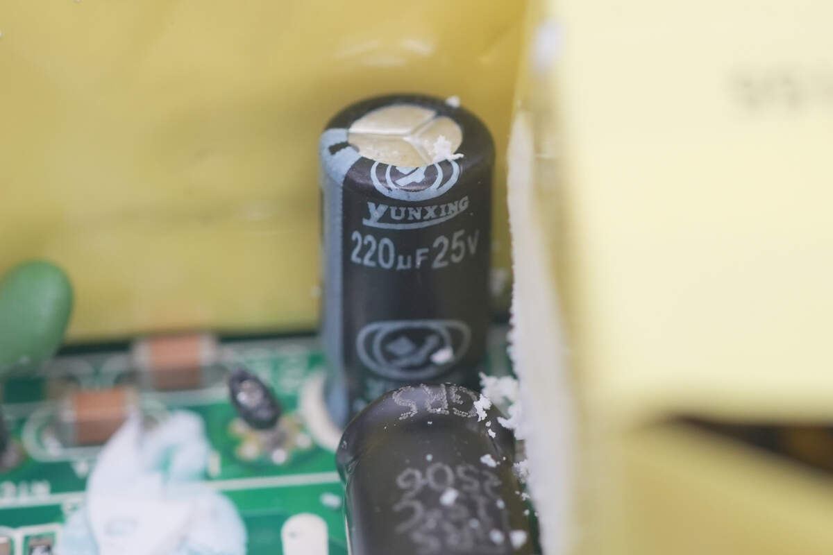
The capacitor supplying power to the master control chip is from YUNXING. 25V 220μF.
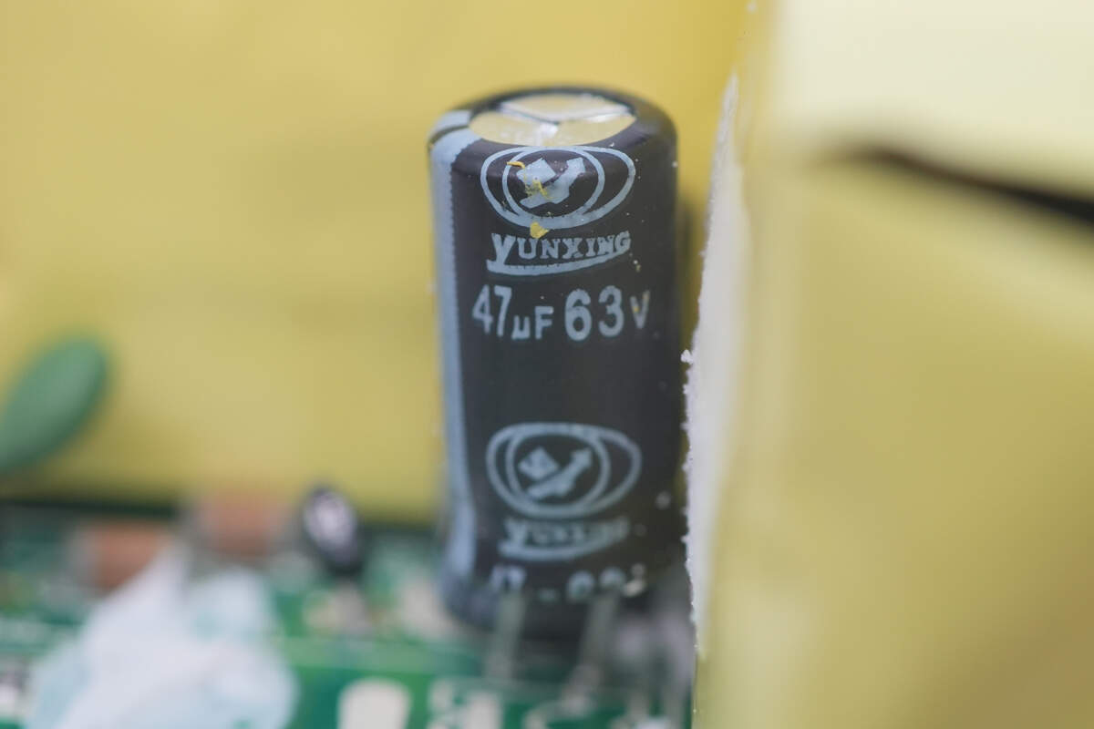
The other capacitor has a specification of 63V, 47μF.
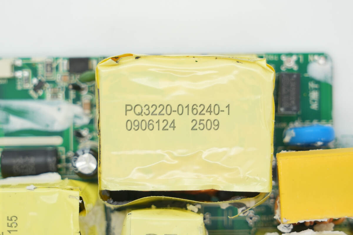
Close-up of LLC transformer.
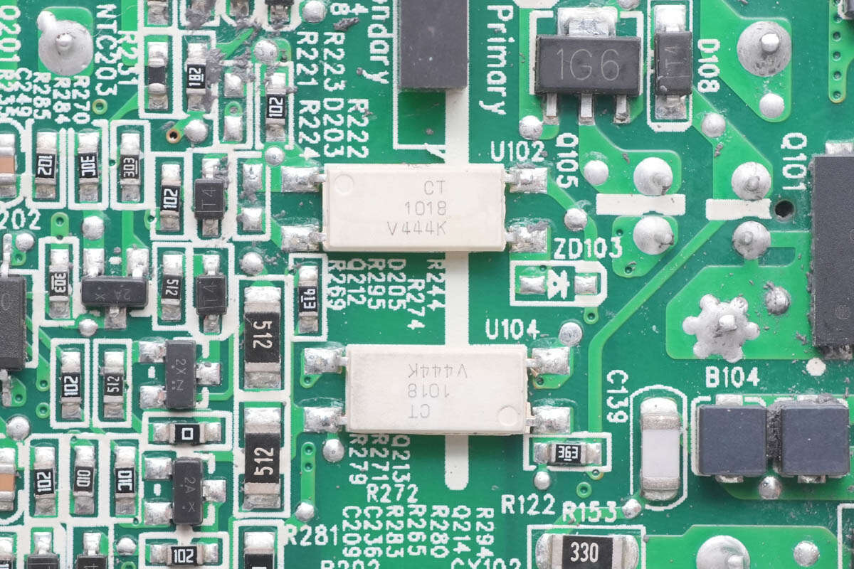
Two CT1018 optocouplers are used for output voltage feedback and function control.
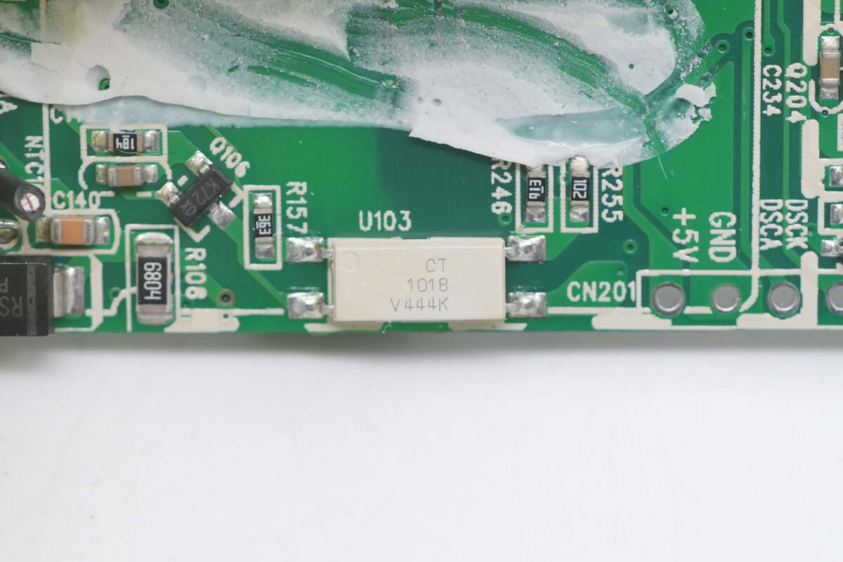
Close-up of the third CT1018 optocoupler.
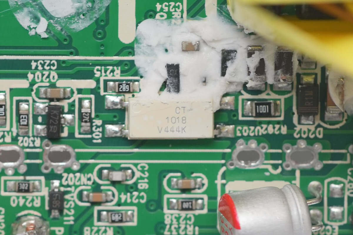
A total of four CT1018 optocouplers are used.
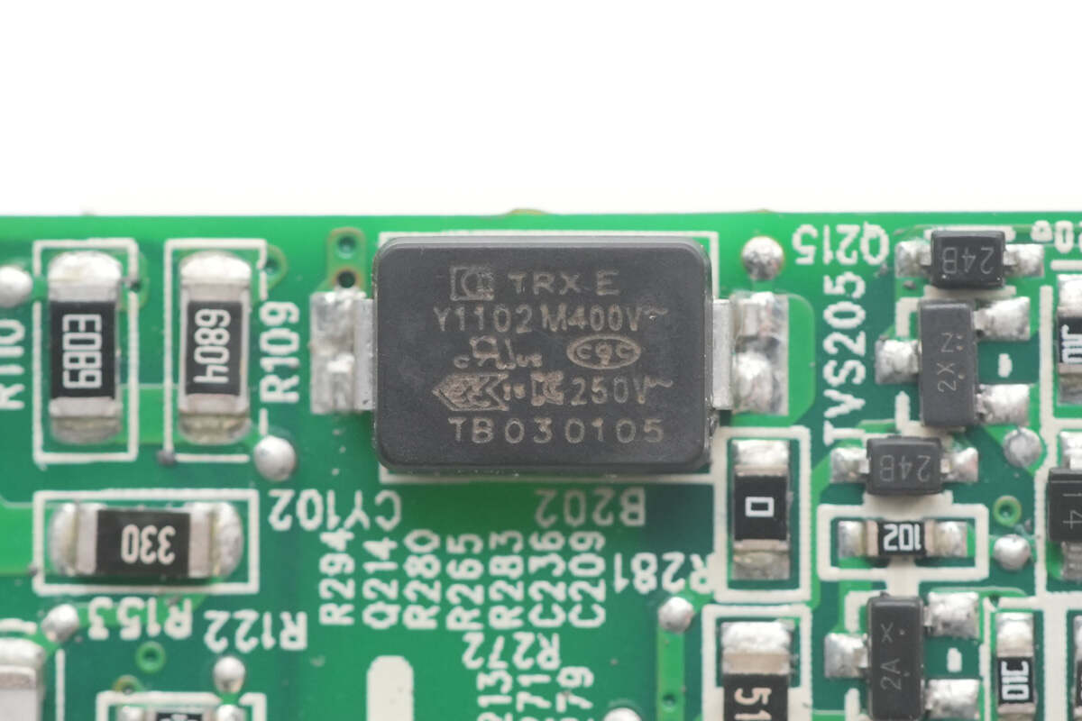
The SMD Y capacitor is from TRX. Its small size and light weight are suitable for high-density power products such as GaN fast chargers. The part number is TMY1102M.
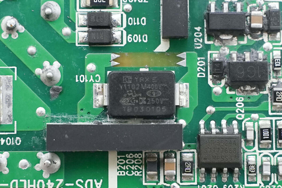
Close-up of the other SMD Y capacitor.
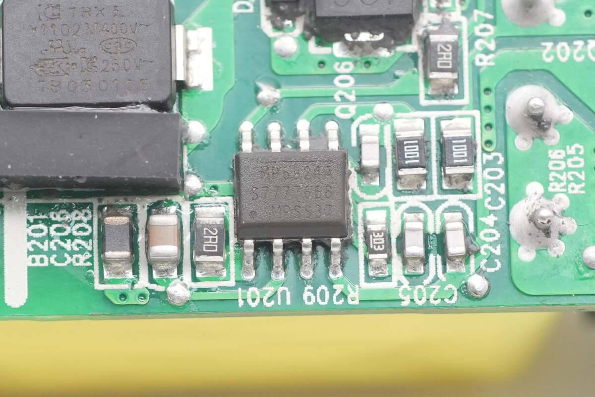
The synchronous rectifier controller is from MPS, model MP6924A. It is an LLC synchronous rectifier controller featuring enhanced interference immunity and fast shutdown capabilities, compatible with CCM/DCM modes. The MP6924A integrates two synchronous rectifier controllers internally, each dedicated to the rectification of the two secondary coils of the LLC converter. It is designed for LLC converter synchronous rectification applications and comes in an SOIC-8 package.
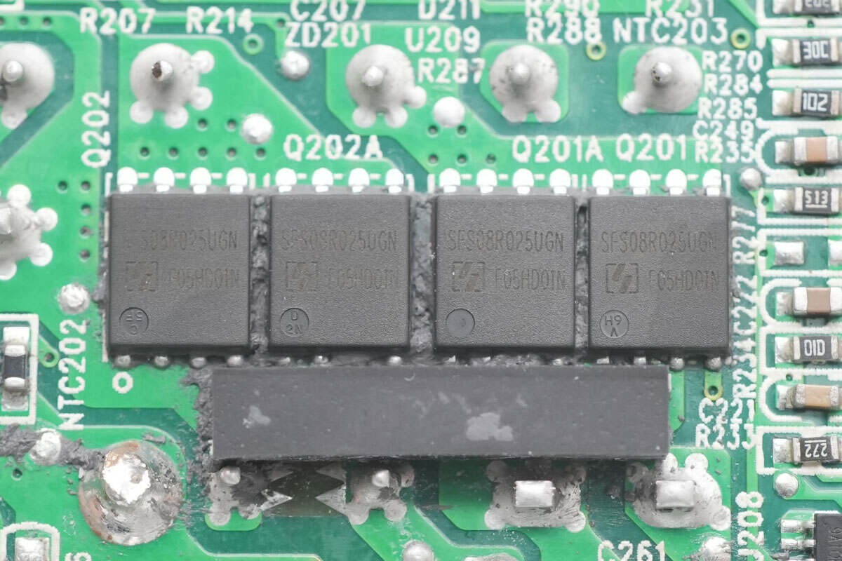
The four synchronous rectifiers are from Oriental, model SFS08R025UGNF. They are NMOS devices with an 80V voltage rating and a 2.5mΩ on-resistance, housed in a PDFN 5×6 package.
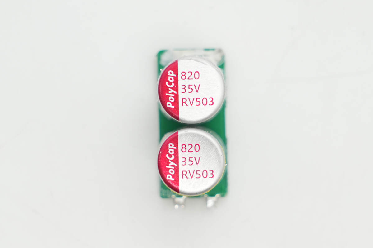
Two solid capacitors for output filtering are from PolyCap, both rated at 35V and 820μF.
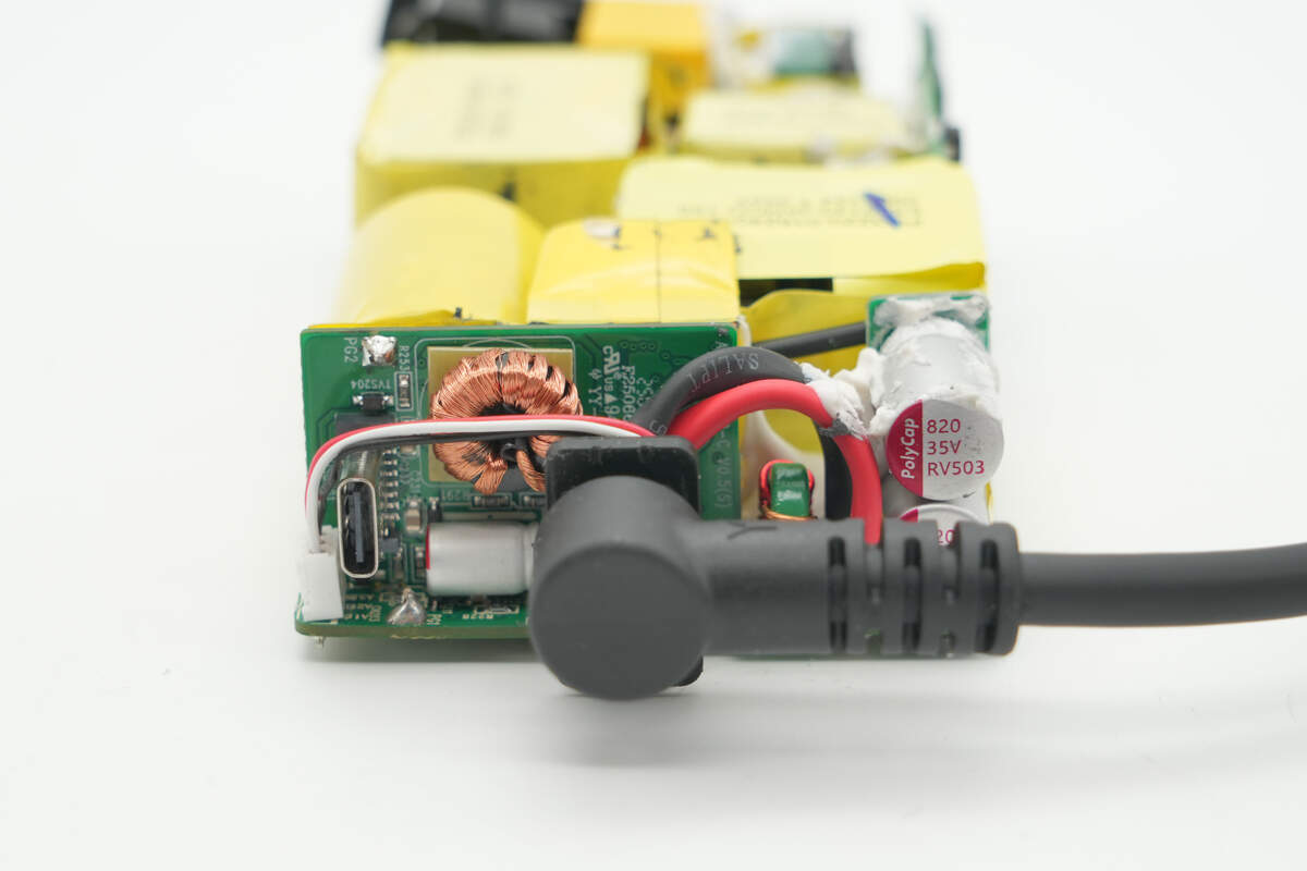
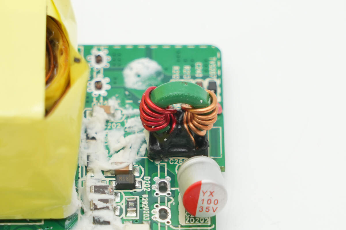
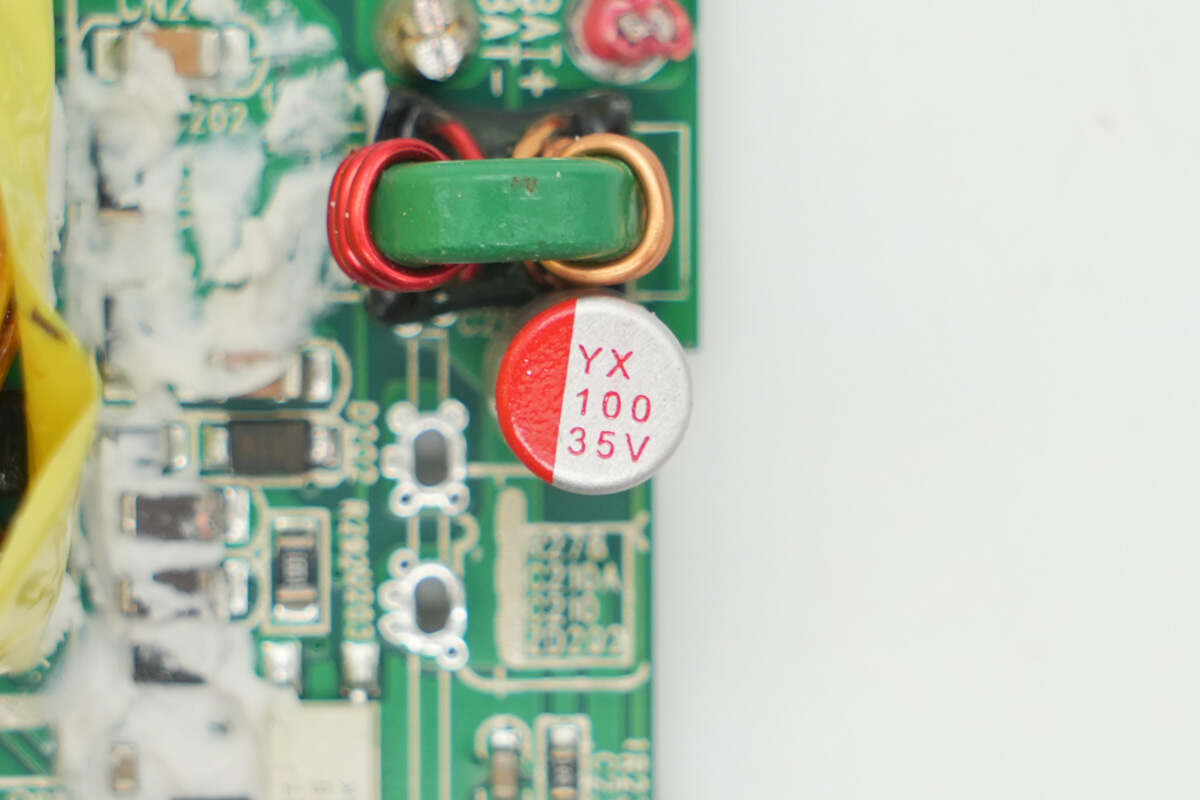
Overview of the output end.
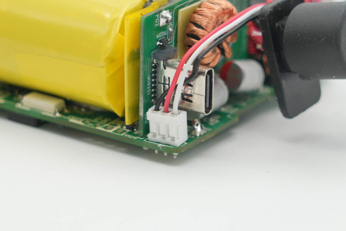
The red, white, and black signal wires are designed as plug-and-play connectors.
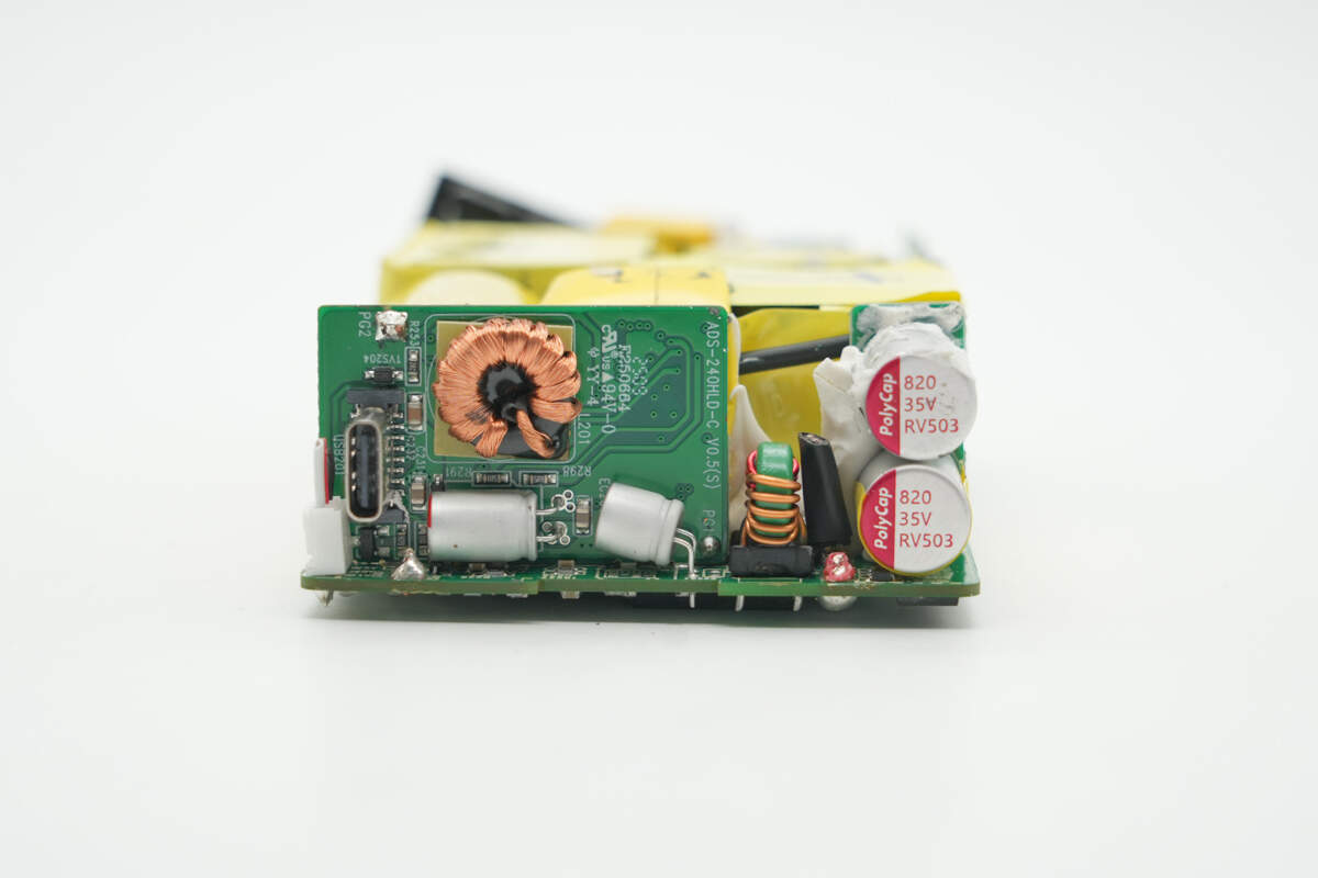
The small PCB at the output end contains a toroidal inductor and a solid capacitor.
The back has a copper heat sink to aid heat dissipation, and it is wrapped with insulating tape.
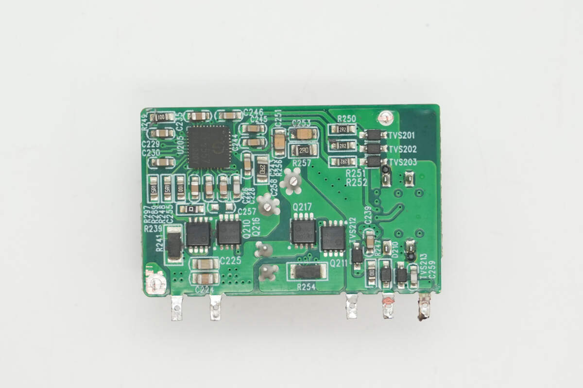
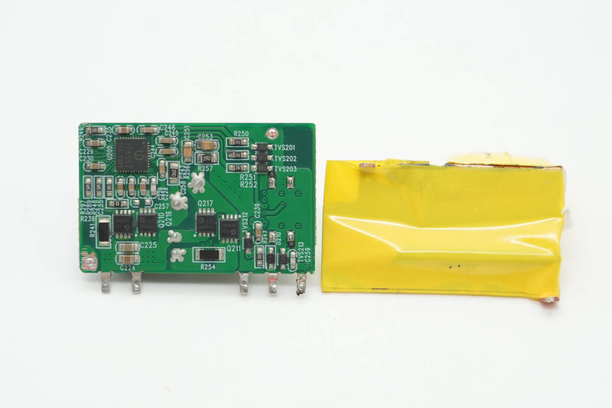
The back side is equipped with a buck-boost protocol chip and synchronous buck-boost MOSFETs.
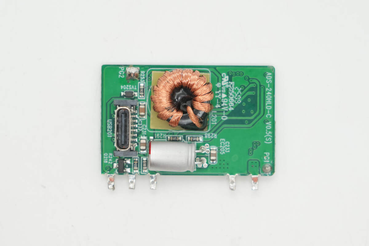
The front features a toroidal inductor, a solid capacitor, and a USB-C socket.
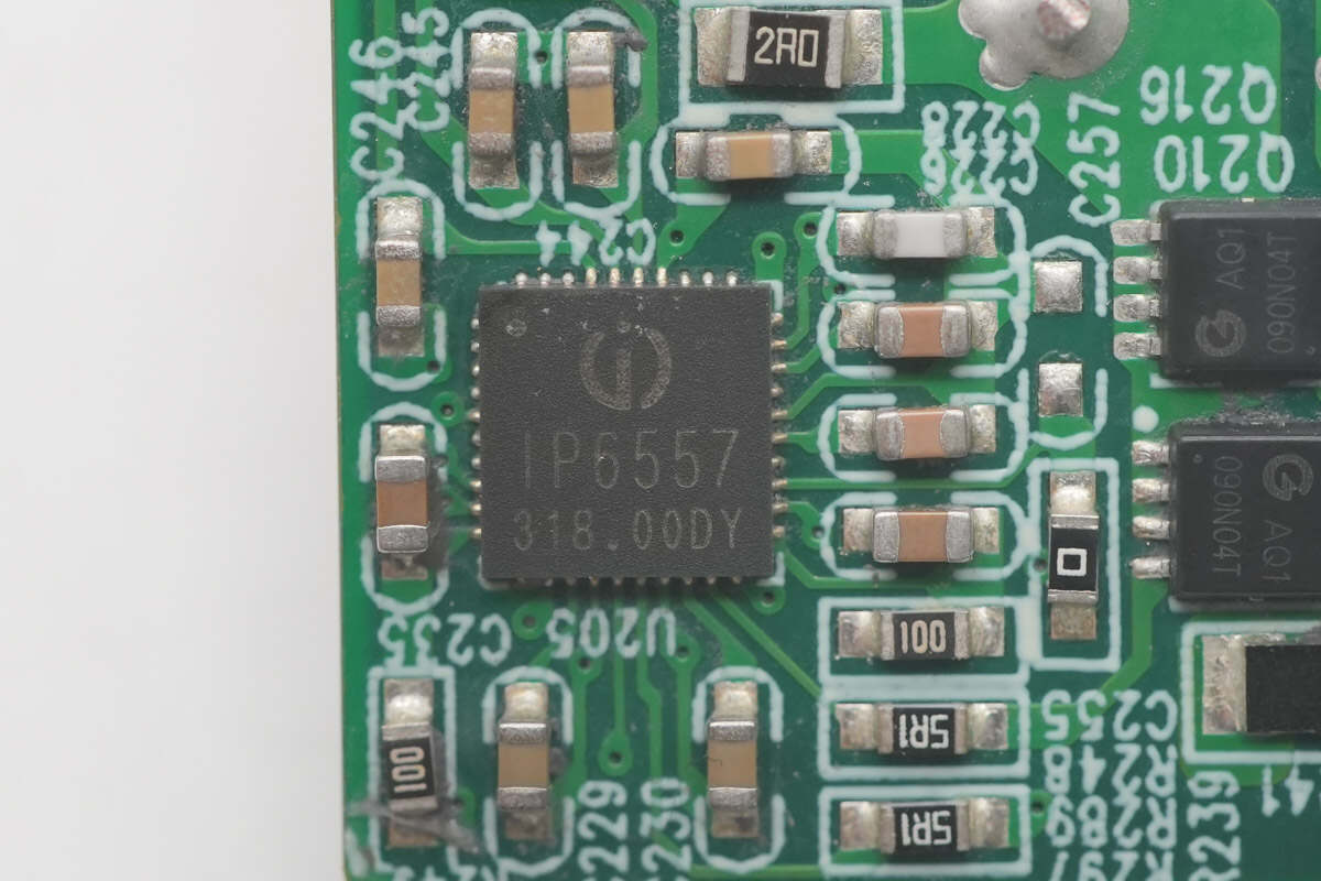
The buck-boost protocol chip is from Injoinic, model IP6557. It is an integrated SOC featuring a buck-boost controller and path NMOS control, supporting QC2.0/3.0/3+/4+/5, FCP, HSCP, AFC, MTK, UFCS, as well as USB-C PD3.1/PPS/ERP28V fast charging protocols. With just one inductor and one power MOSFET, it enables a compact buck-boost fast charging solution that effectively reduces overall size and BOM cost, providing a complete power solution for car chargers.
The integrated buck-boost controller in the IP6557 can deliver up to 140W (28V/5A) output power and supports NTC-based board-level temperature detection to intelligently adjust output power based on temperature. It also includes a built-in 14-bit ADC for precise measurement of input/output voltage, current, and IO voltage.
The IP6557 fast charging output features CV/CC characteristics: when the output current is below the set threshold, it operates in CV mode with constant output voltage; when the output current exceeds the threshold, it switches to CC mode with reduced output voltage. Additionally, it integrates multiple protection functions, including input overvoltage and undervoltage protection, output overvoltage, undervoltage, overcurrent, short circuit, and overtemperature protection. The chip comes in a QFN40 (5mm × 5mm) package.
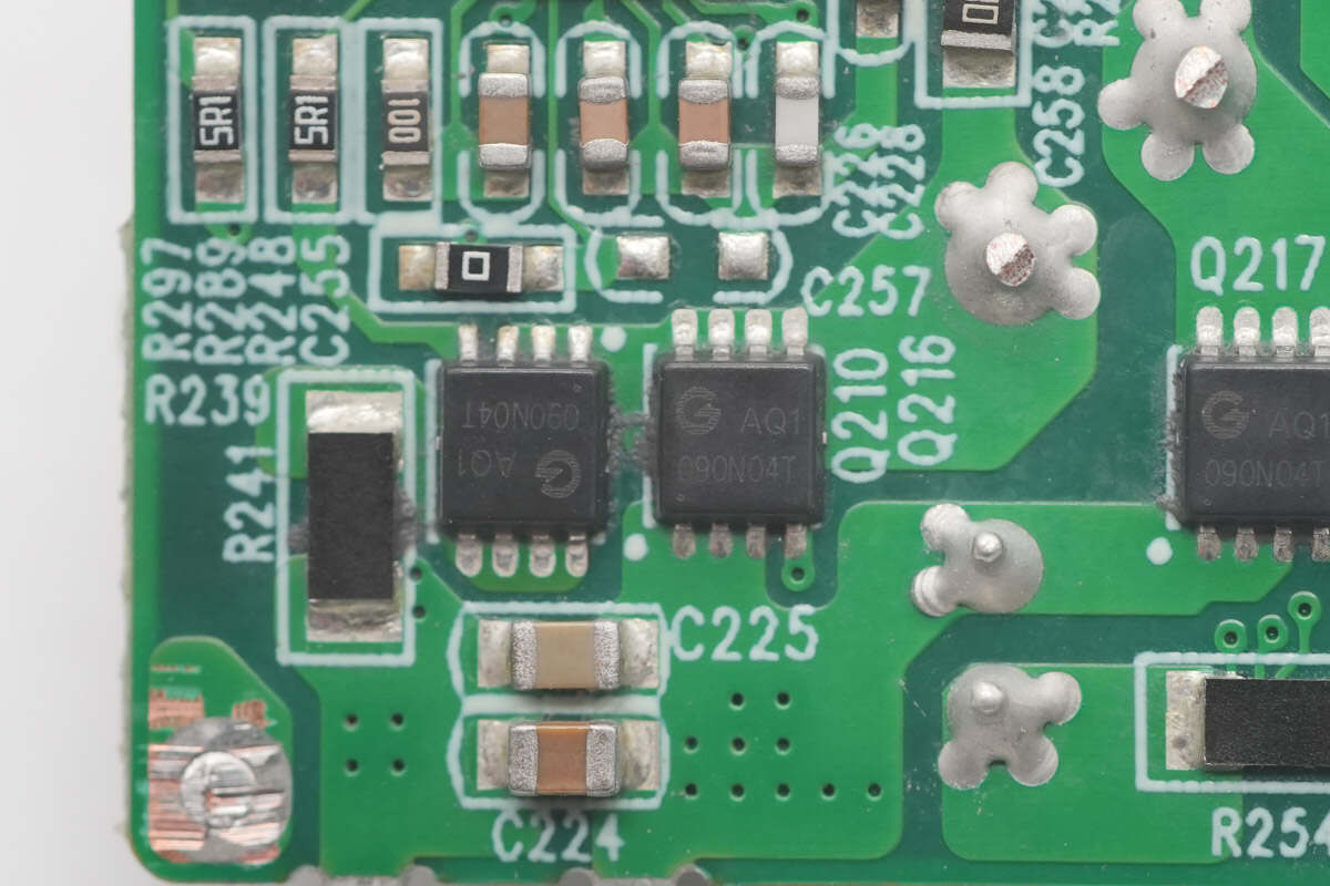
The synchronous buck-boost MOSFET is from Galaxy, model TBL090N04T-3DL8. It is an NMOS device with a 40V voltage rating and a 9mΩ on-resistance, housed in a PDFN 3×3-8L package.
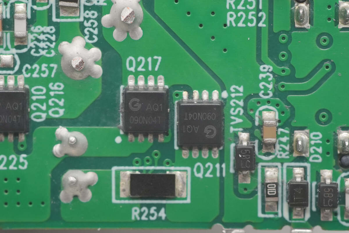
The other two MOSFETs have the same model.
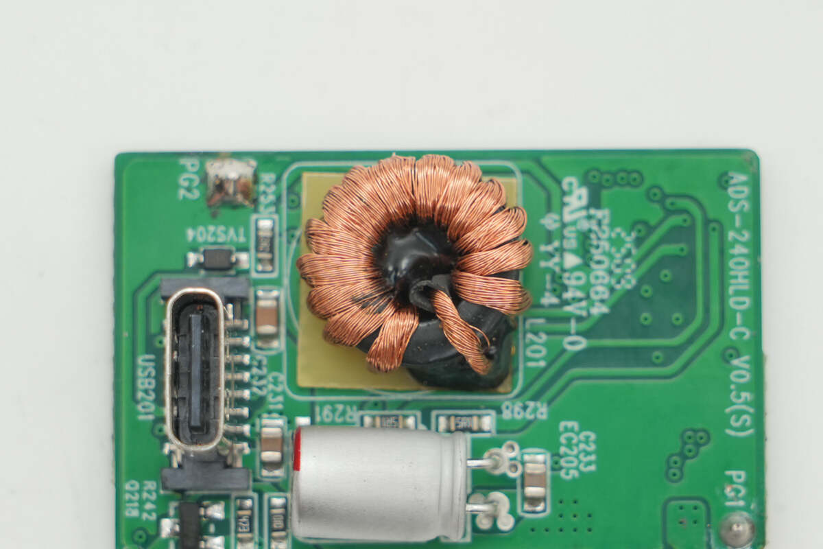
The toroidal inductor is wound with Litz wire, has a bakelite base at the bottom, and is reinforced with adhesive at the center.
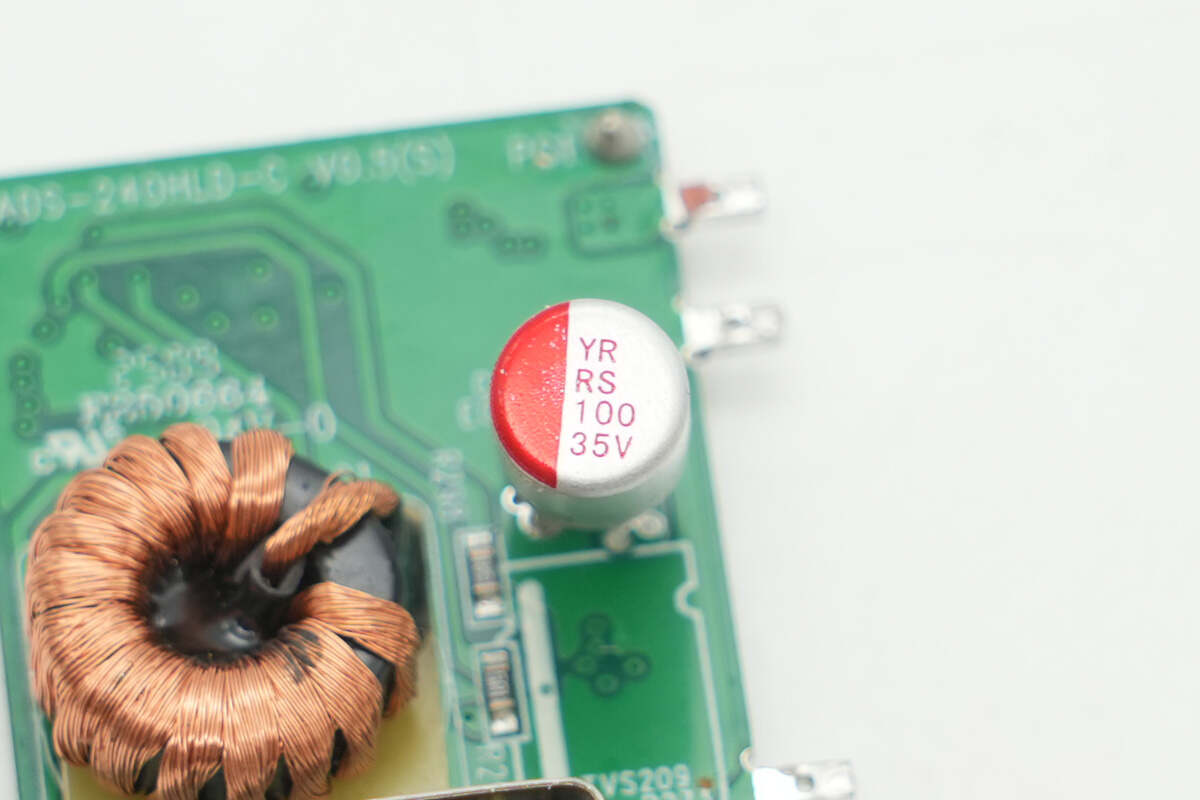
The solid capacitor is rated at 35V, 100μF.
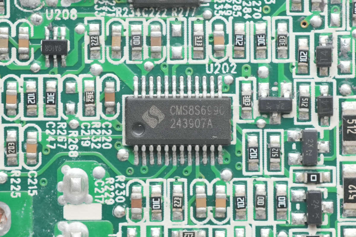
The MCU used for charging control is from Cmsemicon, model CMS8S6990. It is an enhanced 1T 8051 Flash MCU, packaged in SSOP24.
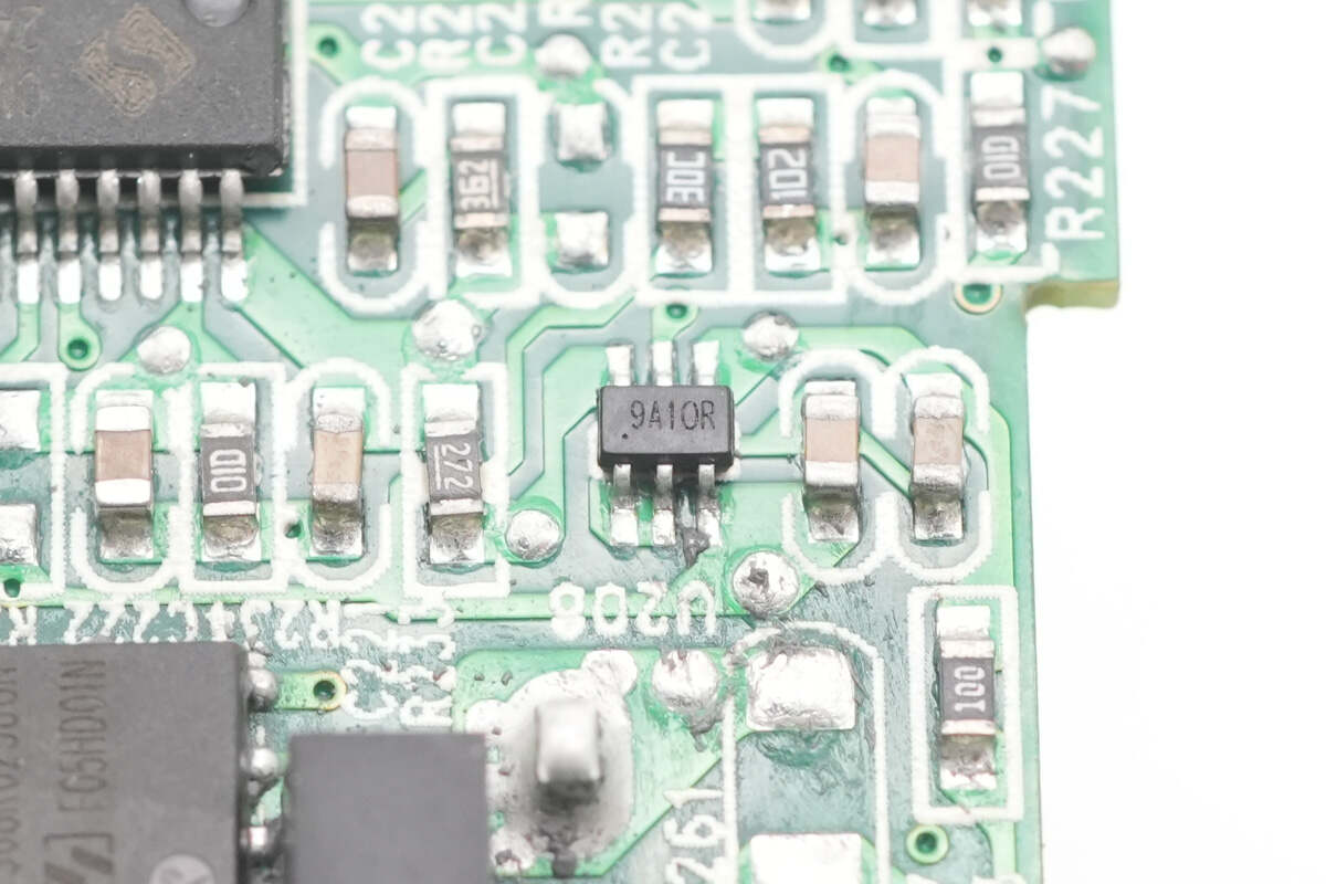
The current sensing chip is from 3PEAK, marked 9A1, model TP181A1. It is a zero-drift, bidirectional current sense amplifier, packaged in SC70.
The filter inductor has an insulating base at the bottom.
The solid capacitor is from YUNXING. 35V 100μF.
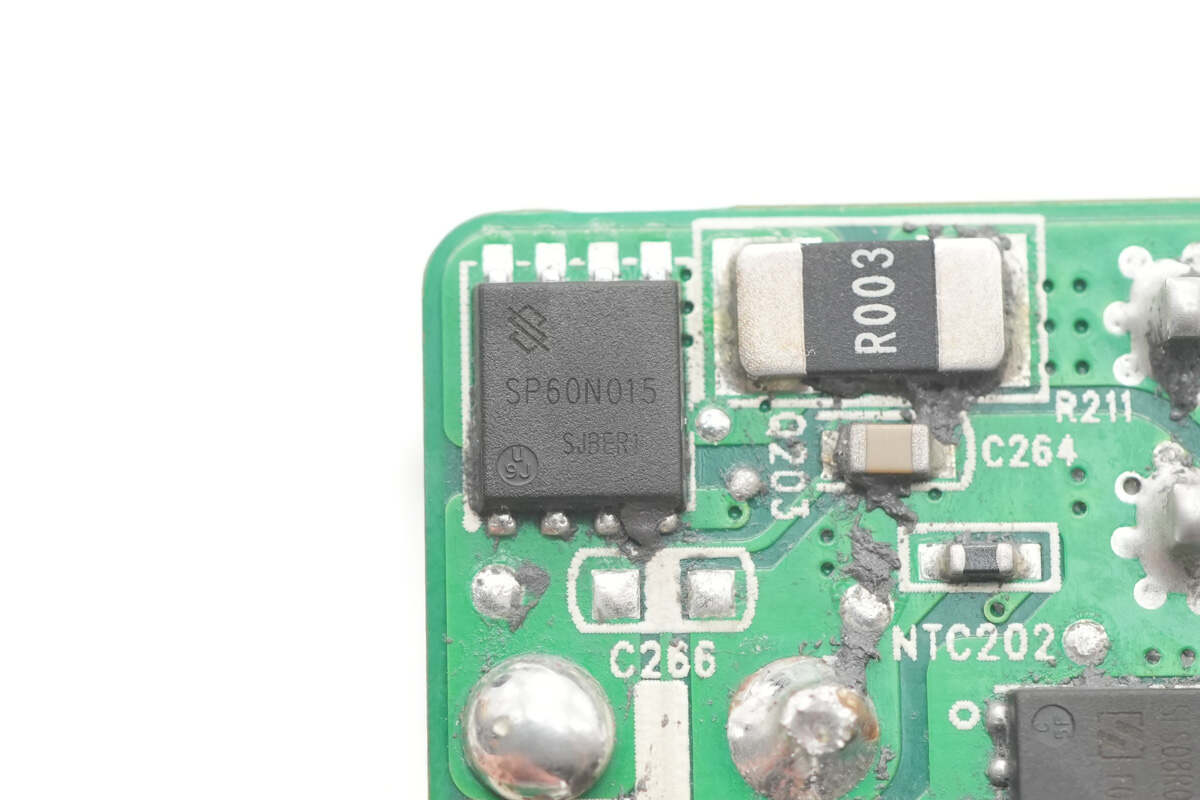
The cable output VBUS MOSFET is marked with SP60N015.
Well, those are all components of the DJI Original 240W Power Adapter for Mavic 4 Pro.
Summary of ChargerLAB
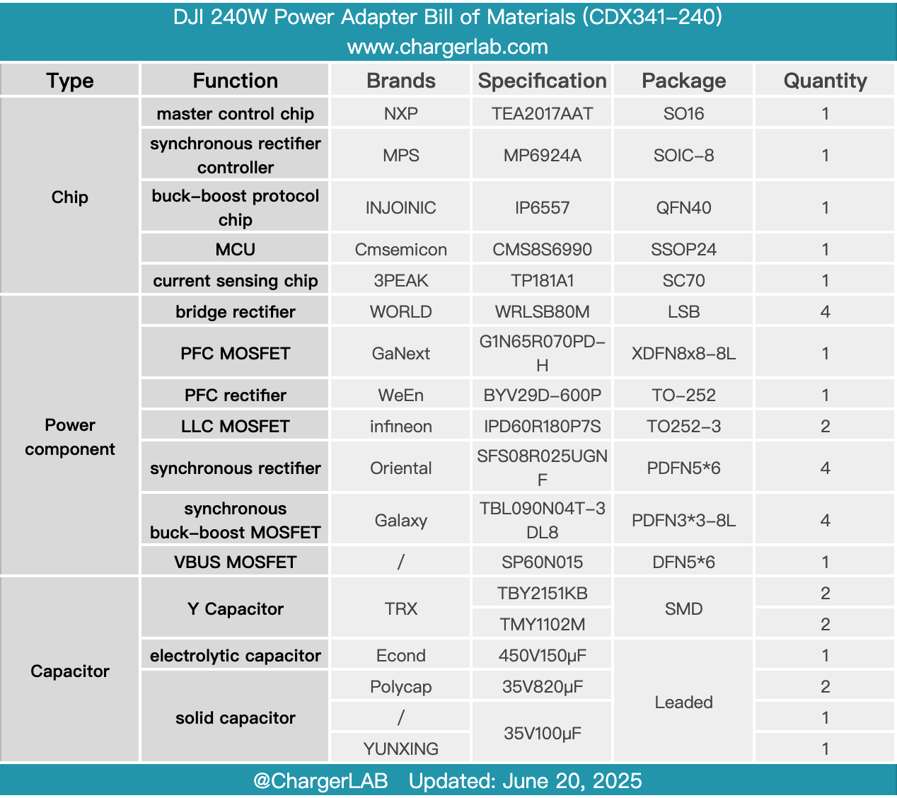
Here is the component list of the DJI Original 240W Power Adapter for Mavic 4 Pro for your convenience.
Thanks to the GaN technology, even with an output power of up to 240W, the device remains relatively compact. The power cable features a detachable design, offering greater flexibility, and comes with a Mini SDC charging cable compatible with DJI outdoor power supplies. The USB-C fast charging port supports mainstream fast charging protocols and delivers up to 140W PD3.1 fast charging. Its excellent compatibility and powerful performance significantly expand the range of devices it can support. While providing battery power for outdoor aerial photography, it can also fast-charge users' smartphones, tablets, and laptops, making it highly practical.
After taking it apart, we found that it features a high-efficiency topology based on the NXP TEA2017AAT master control chip combined with the MPS MP6924A synchronous rectifier controller. The PFC boost circuit uses the GaNext G1N65R070PD-H, further improving power efficiency and power density. The LLC MOSFET and synchronous rectifiers are sourced from Infineon and Oriental.
At the output end, charging control is managed by a Cmsemicon MCU, while the Injoinic IP6557 buck-boost protocol chip ensures excellent compatibility and high performance for the USB-C port. The entire module has a compact component layout, reinforced and thermally bonded with adhesive. Additionally, it uses a dual-layer heat sink and copper foil for effective heat dissipation, addressing thermal challenges during high-power operation. The materials and workmanship are highly reliable.
Related Articles:
1. Teardown of CUKTECH 30 Charging Station Ultra (TA3005U)
2. Teardown of Huawei 100W SuperCharge GaN Charger (HW-200500C03)
3. Teardown of Lenovo Legion Go S Gaming Console