Introduction
DJI has launched a new product, the DJI POWER 1000 V2 power station. It features a 1 kWh lithium iron phosphate battery and a 2600W inverter output power. It is equipped with two universal three-prong sockets and two two-prong sockets, capable of powering high-load electrical appliances. The inverter includes a UPS function with an upgraded switching time of 0.01 seconds.
It supports charging via AC mains, solar panels, and car charging. AC charging can charge the battery up to 80% in 37 minutes and fully in 56 minutes. Solar charging supports a maximum power of 1800W and can fully charge the battery in as fast as 40 minutes. Car charging supports up to 1000W and takes 78 minutes to fully charge. It also supports expansion by connecting additional battery packs.
The power station includes both USB-C and USB-A ports, with the USB-C port supporting 140W output. The inverter is protected by a 10 mm-thick potting compound.
Next, we will present a teardown to take a closer look at its internal design and components.
Product Appearance
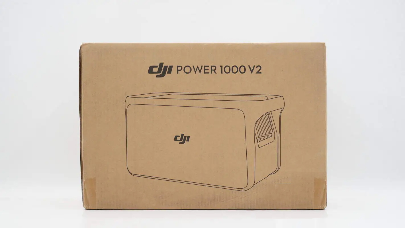
The DJI POWER 1000 V2 is packaged in a corrugated cardboard box.
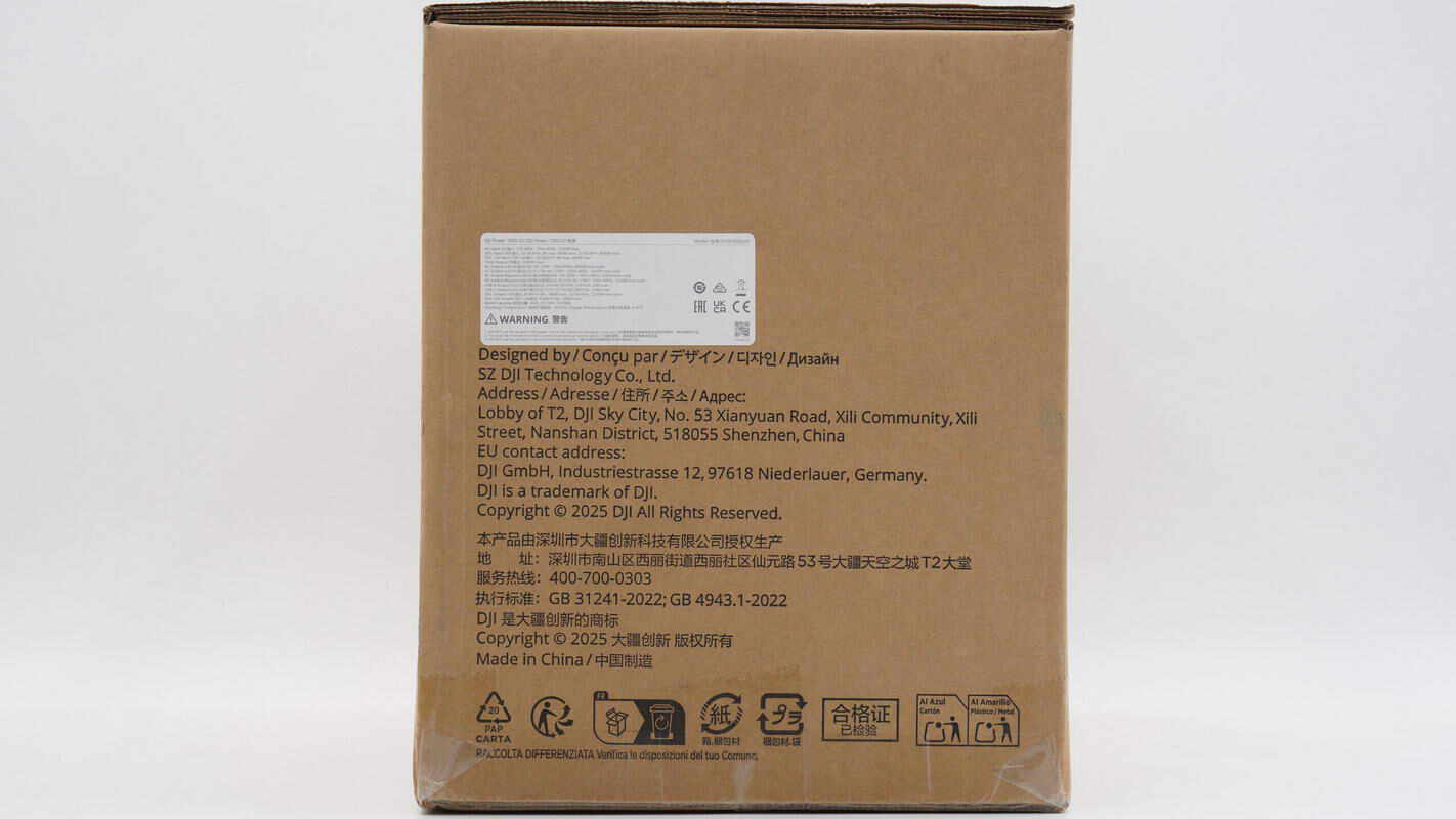
An information label is affixed to the side, which also has basic product details printed on it.
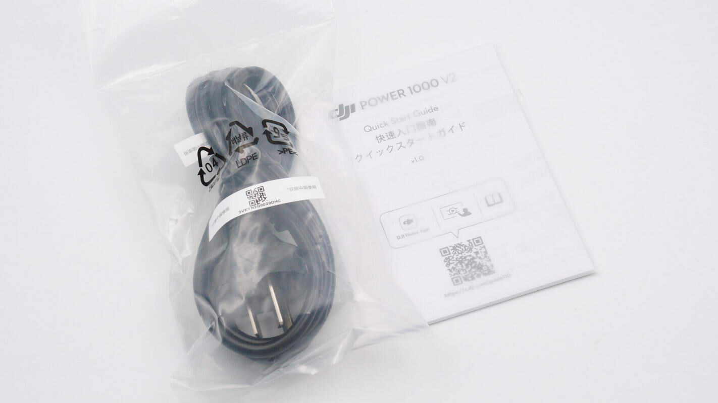
The packaging box includes a power cord and a quick-start guide.
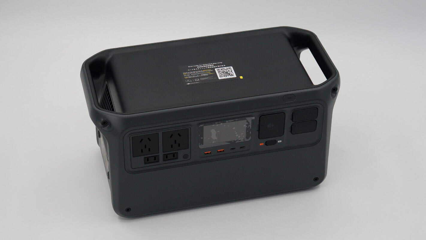
It features a color scheme of black and light gray. With a comprehensive set of ports, a 1 kWh capacity, and a powerful 2600W output, it meets the power needs for all outdoor scenarios.
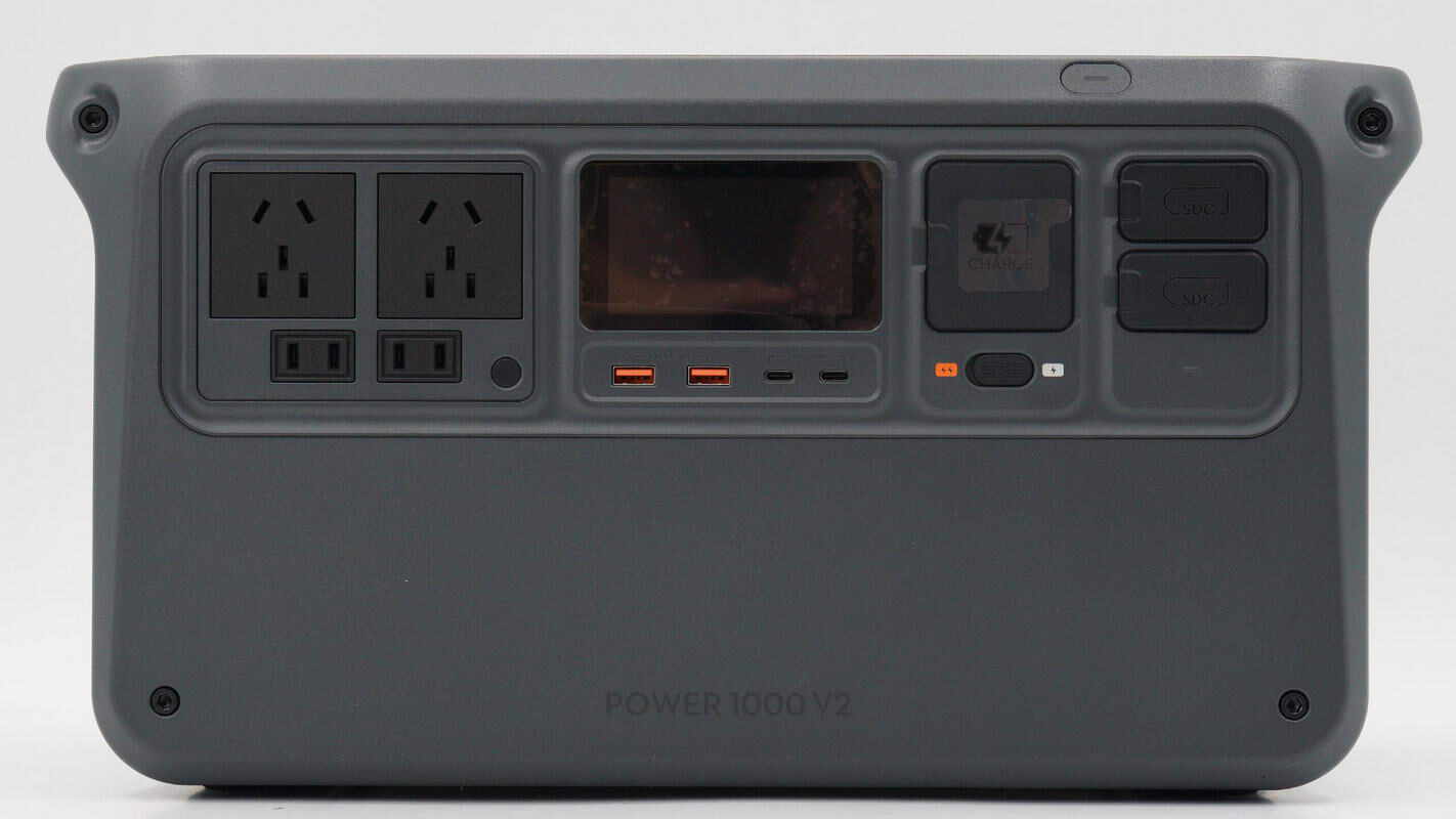
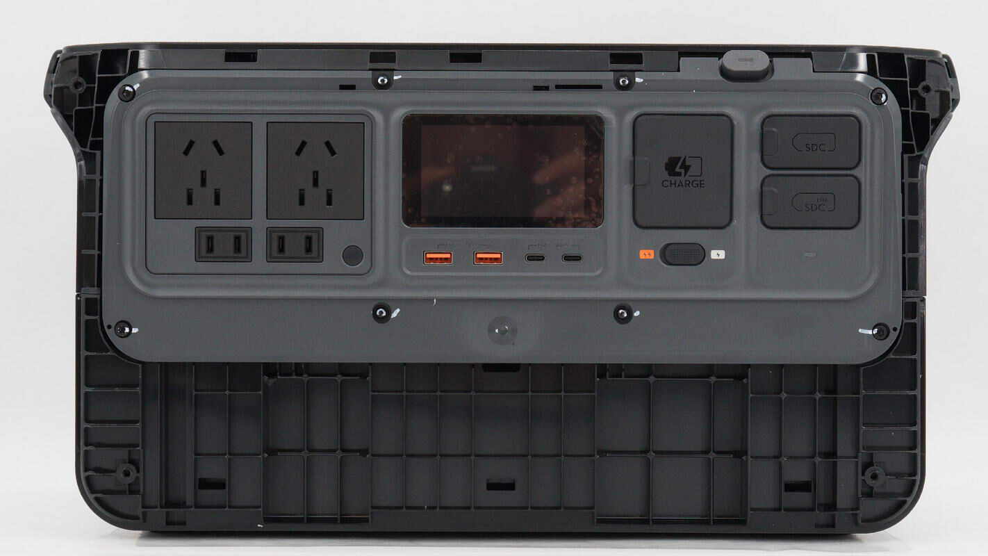
Below the LCD screen in the center of the front panel are the USB-A and USB-C ports. On the left side are the AC output sockets, while the right side houses the AC input socket and the SDC port.
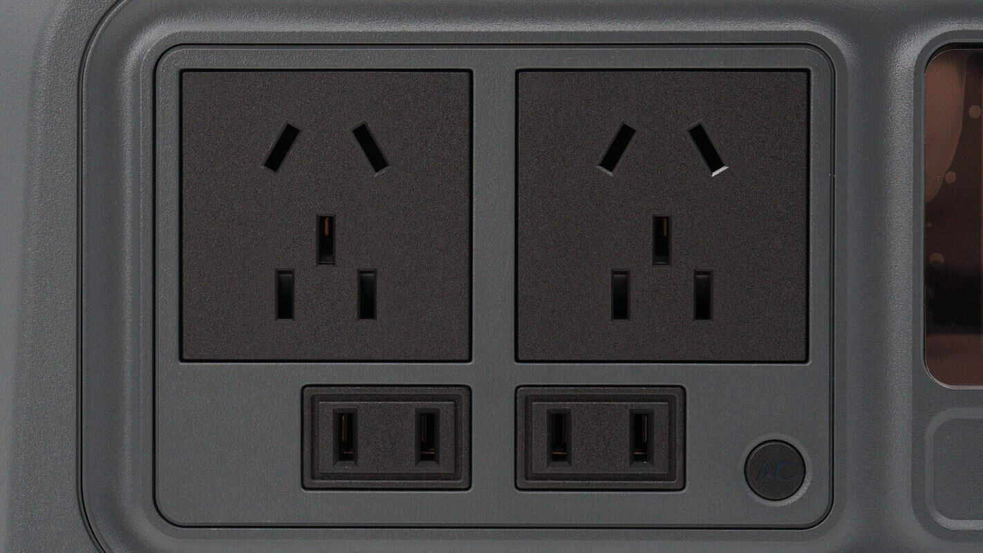
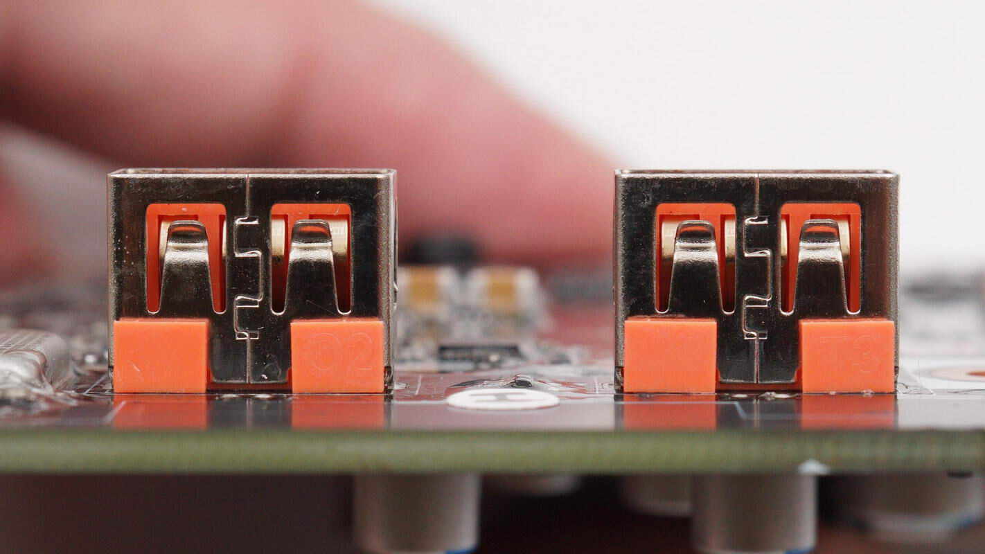
It has two universal three-prong sockets and two two-prong sockets. In the lower right corner, there is an output switch with an indicator light inside.
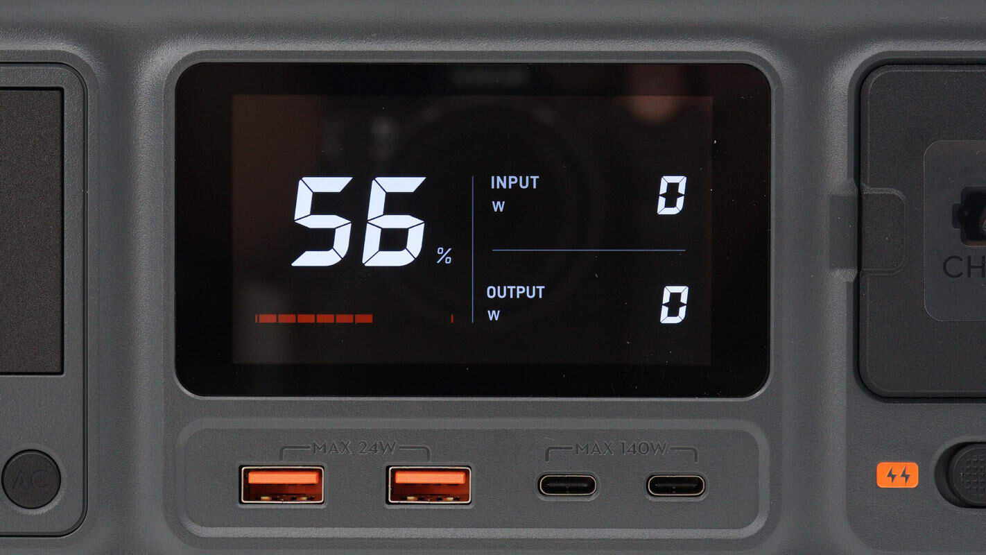
The screen can display remaining capacity, output power, usage duration, input power, and estimated charging time. The USB-A ports support 24W fast charging, and the USB-C port supports 140W fast charging. Additionally, the USB-C port on the left side allows for firmware upgrades via configuration software.
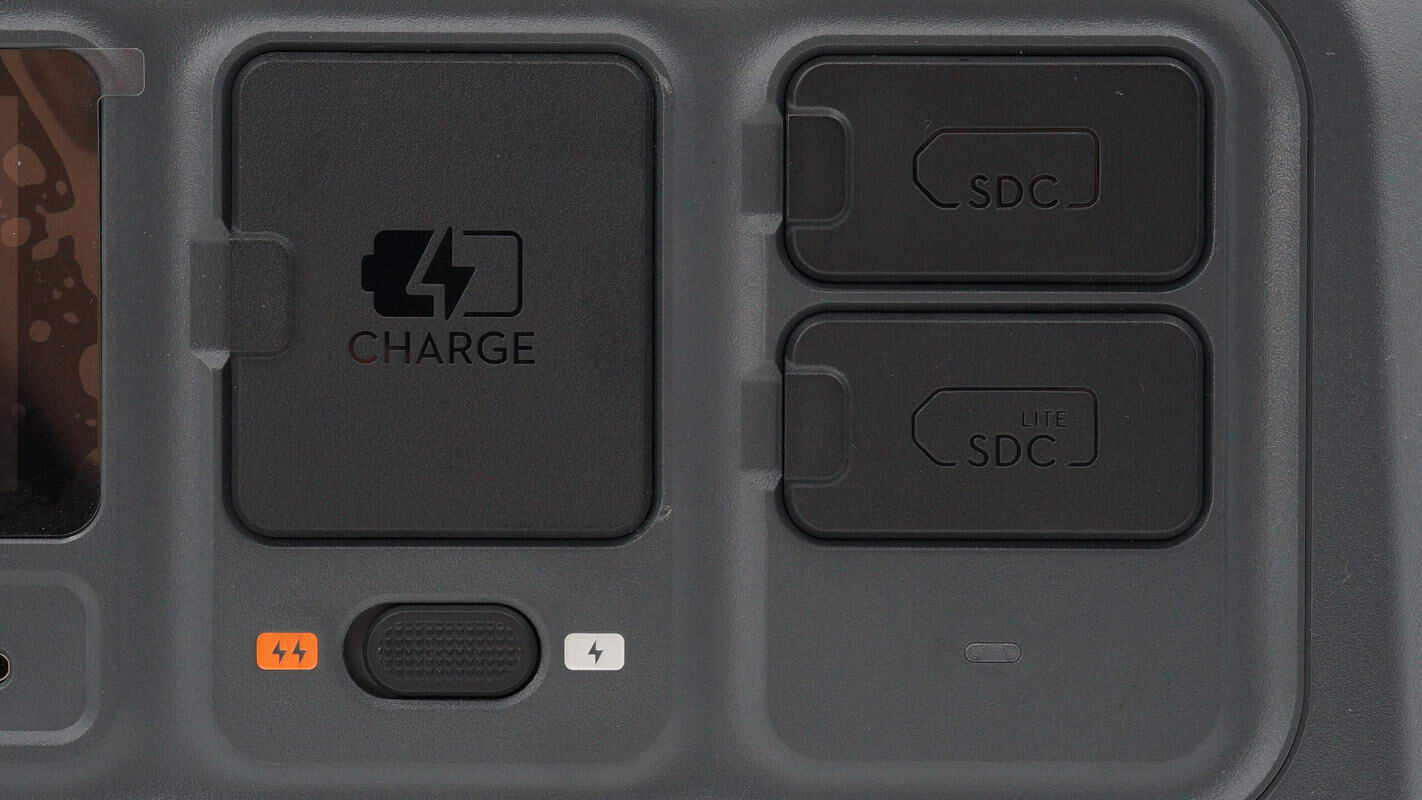
The AC input port, SDC port, and SDC Lite port on the right side all have protective covers to prevent dust and moisture. Below the AC input port, there is also a switch to toggle between fast charging and normal charging modes.
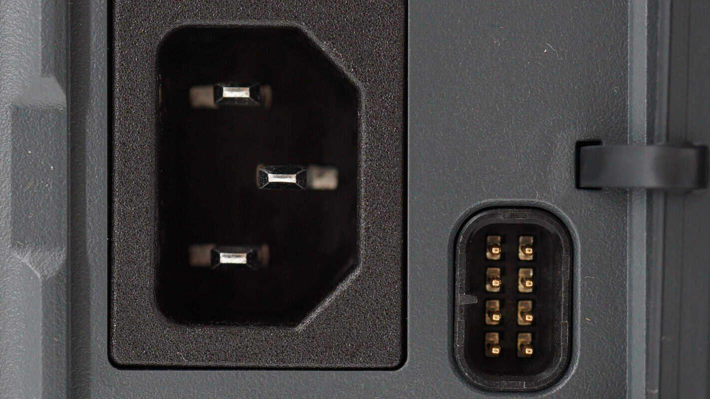
The AC charging input port has a reserved terminal on its right side.
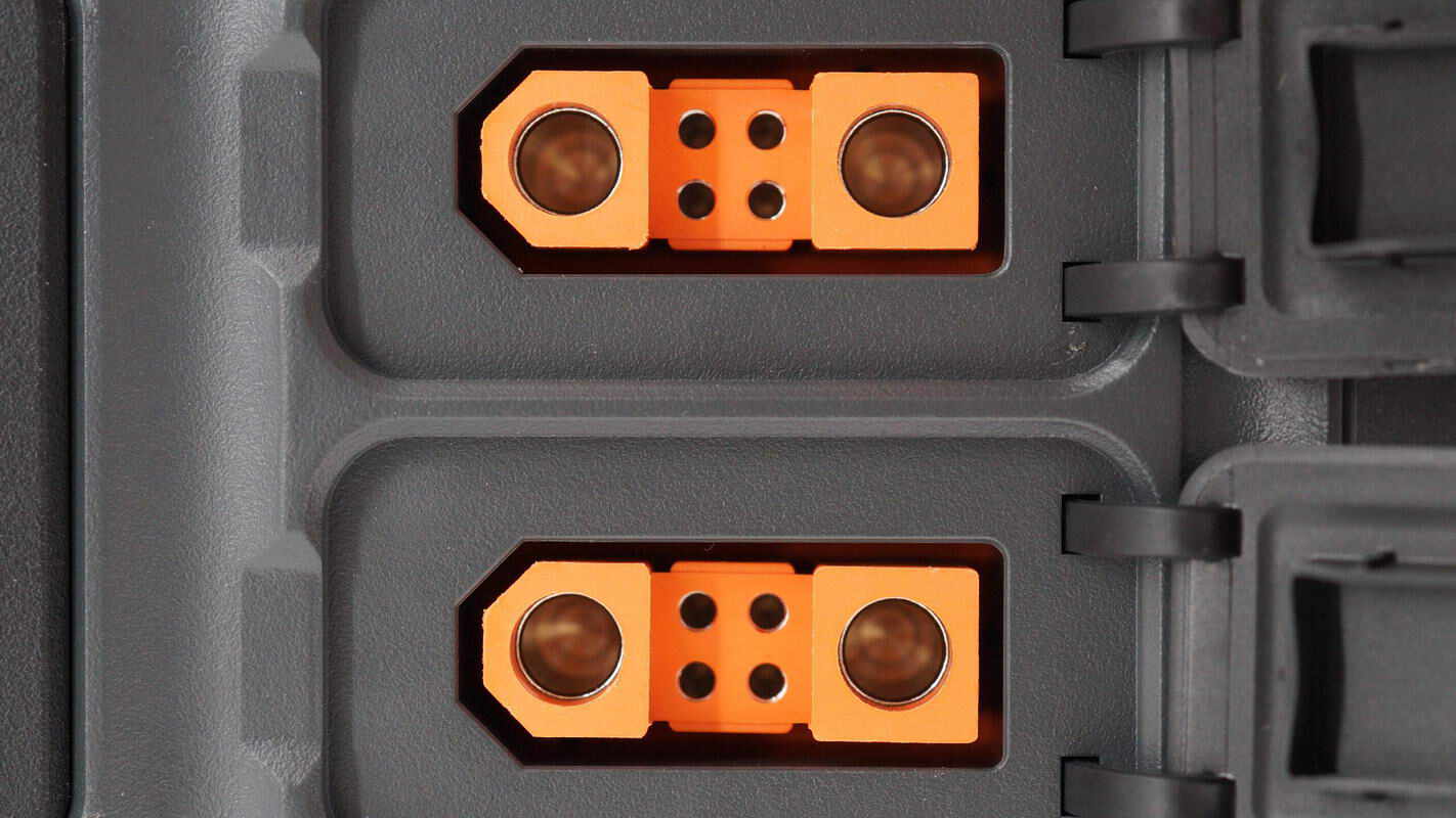
The SDC and SDC Lite ports are arranged vertically and can connect to DJI’s fast charging devices. They also support connecting battery packs, car chargers, and solar panels.
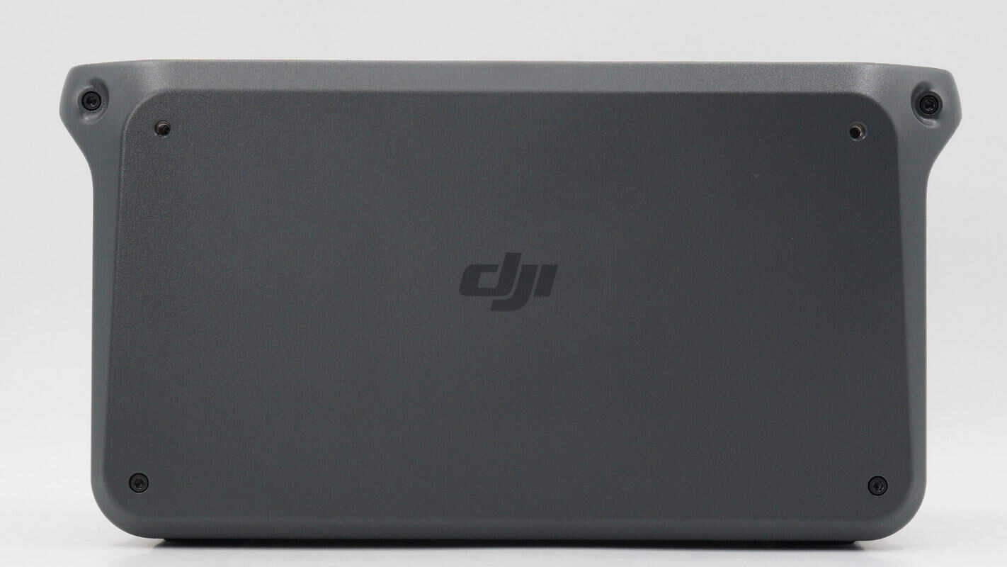
The back features the DJI logo.
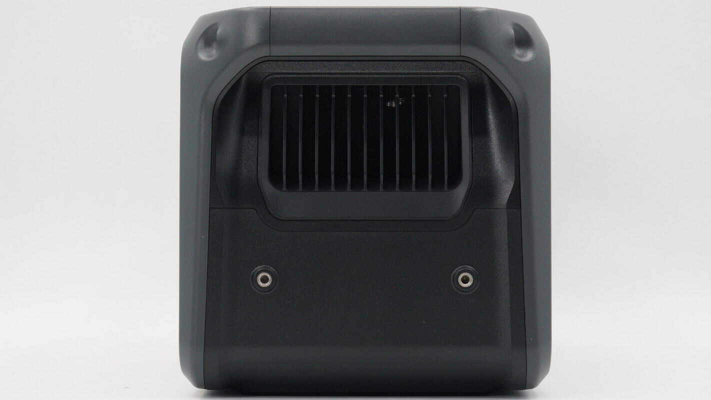
There are ventilation grilles on the side.
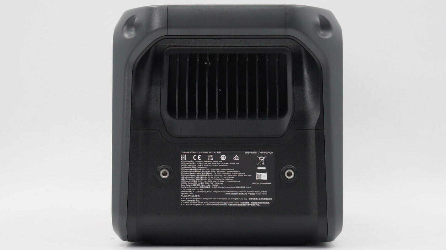
The other side also features ventilation grilles, with a spec info label affixed at the bottom.
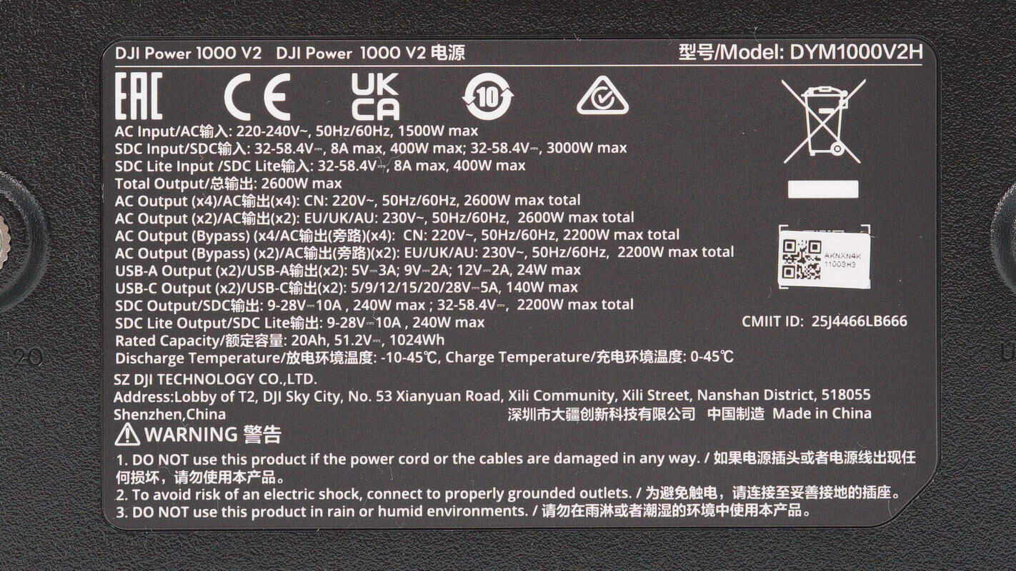
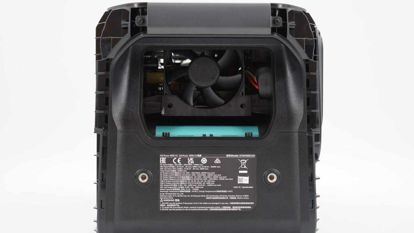
Model: DYM1000V2H
AC Input: 220-240V~, 50/60Hz, 1500W max
SDC Input: 32-58.4V, 8A max, 400W max;32-58.4V, 3000W max
SDC Lite Input: 32-58.4V, 8A max, 400W max
Total Output: 2600W max
AC Output (x4) : CN: 220V~, 50/60Hz, 2600W max total
AC Output (x2) : EU/UK/AU: 230V~, 50/60Hz, 2600W max total
AC Output (Bypass) (x4) : CN: 220V~, 50/60Hz, 2200W max total
AC Output (Bypass) (x2) : EU/UK/AU: 230V~, 50/60Hz, 2200W max total
USB-A Output (x2) : 5V3A, 9V2A, 12V2A;24W max
USB-C Output (x2) : 5/9/12/15/20/28V5A;140W max
SDC Output: 9-28V10A, 240W max;32-58.4V, 2200W max total
SDC Lite Output: 9-28V10A, 240W max;
Rated Capacity: 20Ah, 51.2V, 1024Wh
Discharge Temperature: -10-45℃
Charge Temperature: 0-45℃
Manufacturer: Shenzhen DJI Technology Co., Ltd.
It is EAC, UKCA, CE, RCM certified.
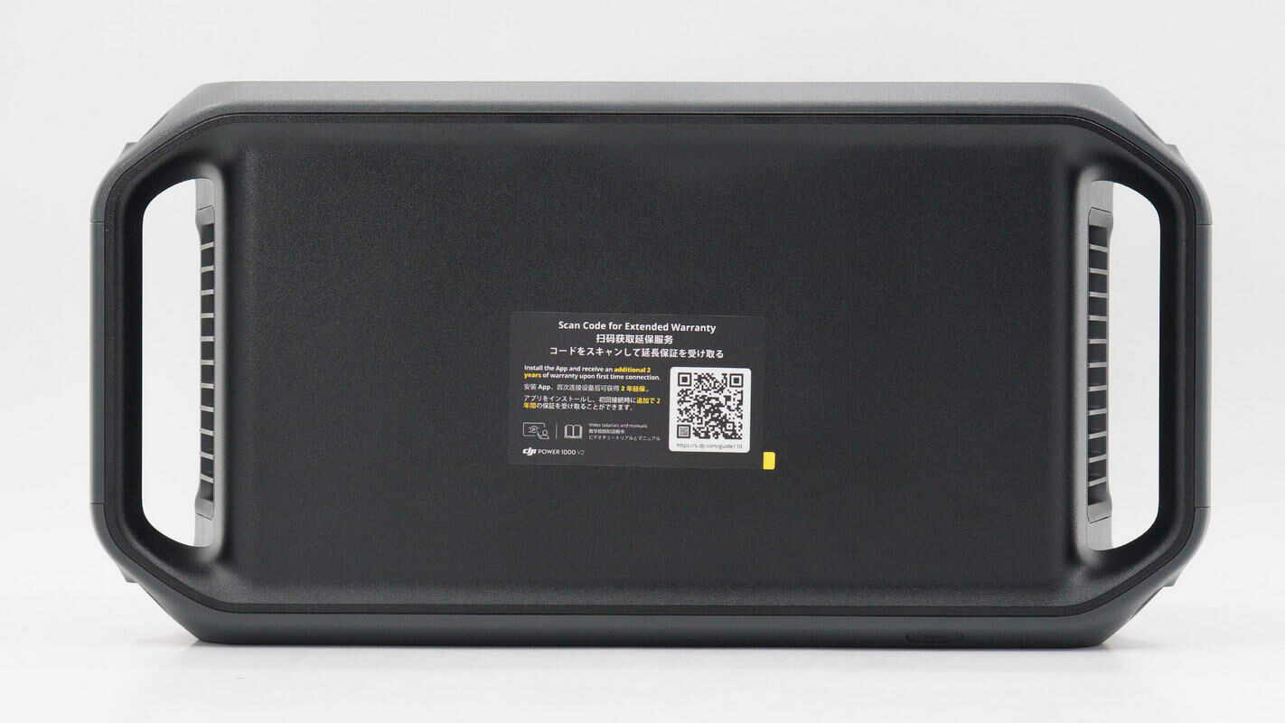
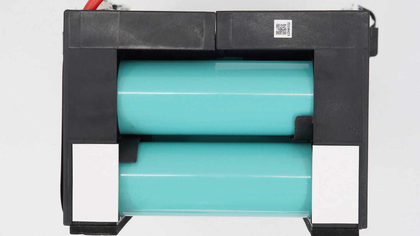
A QR code sticker for extended warranty is affixed to the top, and integrated carrying handles are located on both sides.

Close-up of the integrated carrying handle.
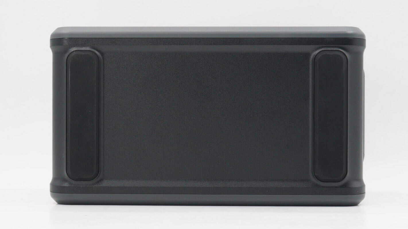
The bottom is equipped with non-slip rubber pads.
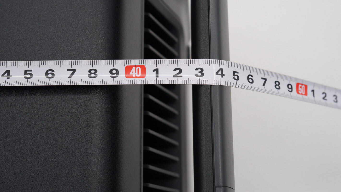
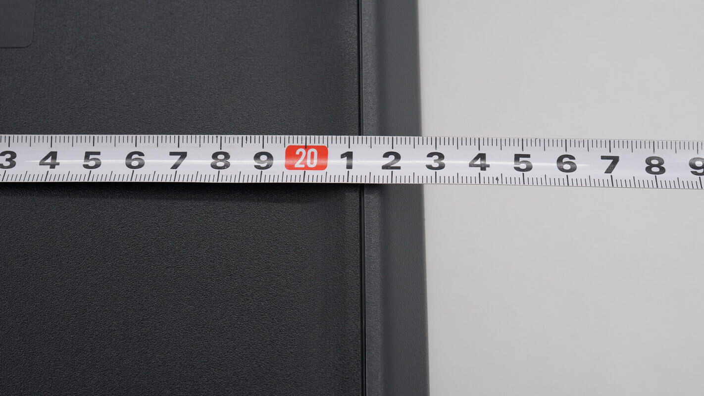
The length is about 446 mm (17.56 inches).
The width is about 228 mm (8.98 inches).
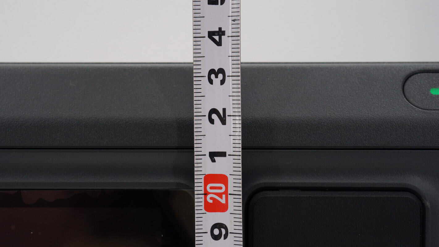
The height is about 234 mm (9.21 inches).

The weight is about 14.25 kg (31.4 pounds).
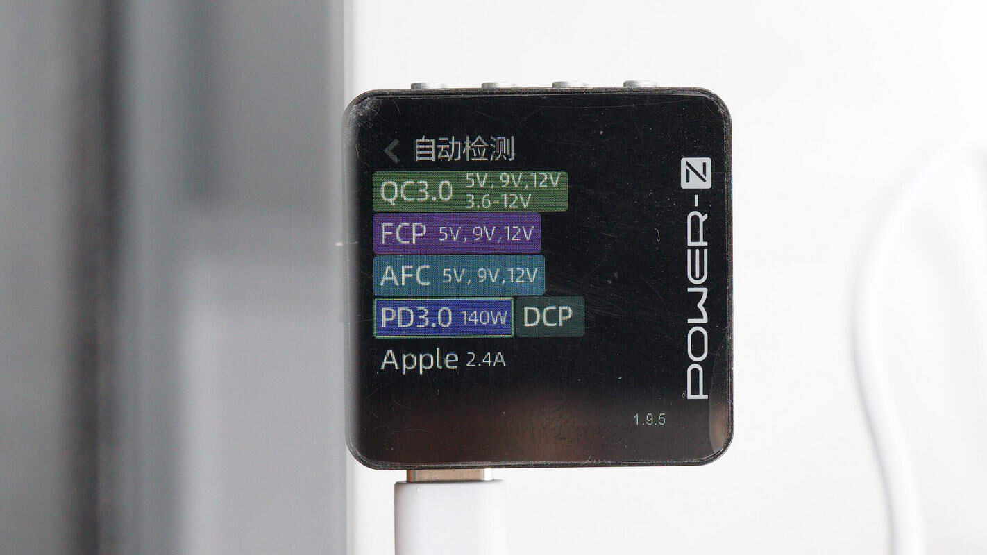
ChargerLAB POWER-Z KM003C shows that the USB-C supports QC3.0, FCP, AFC, PD3.0, DCP, and Apple 2.4A protocols.
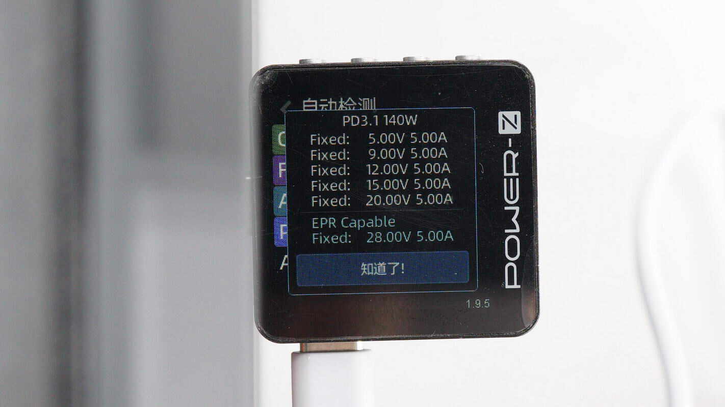
It supports six fixed PDOs of 5V5A, 9V5A, 12V5A, 15V5A, 20V5A, and 28V5A.
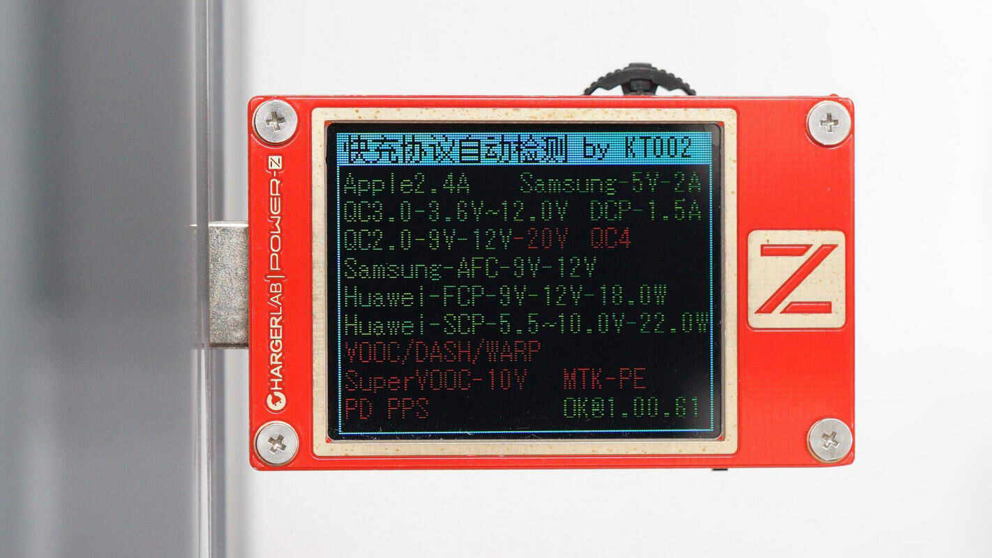
ChargerLAB POWER-Z KM003C shows that the USB-A supports FCP, SCP, AFC, QC3.0, and DCP protocols.
Teardown
Next, let's take it apart to see its internal components and structure.
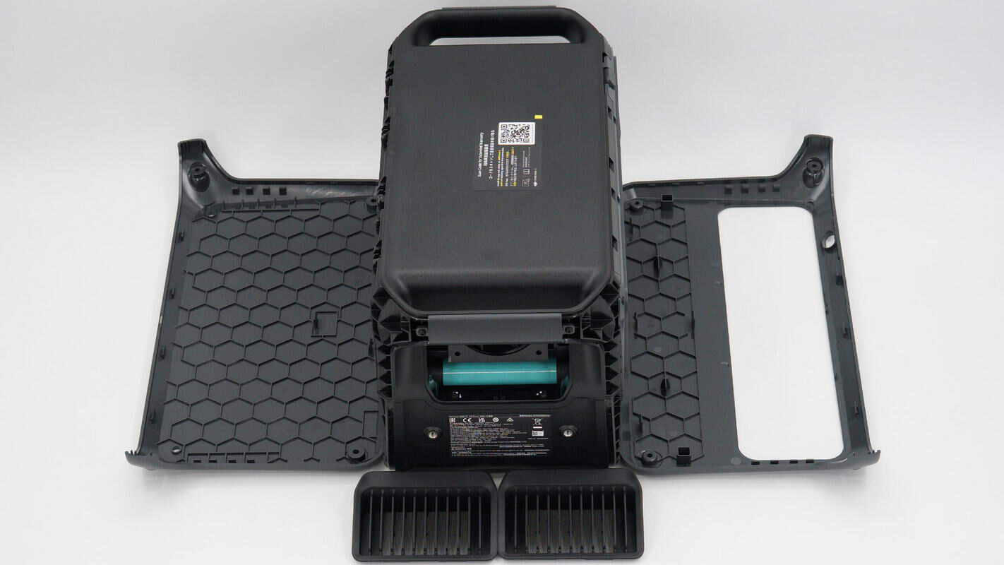
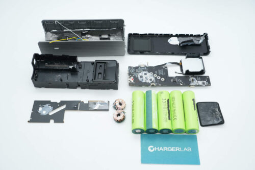
First, unscrew the screws at the four corners, then remove the front and rear cover panels.
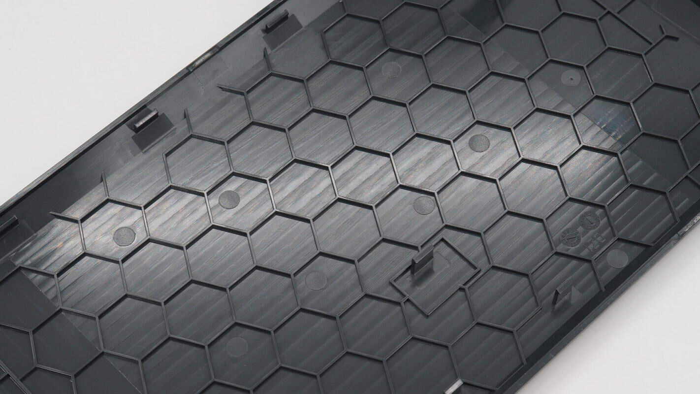
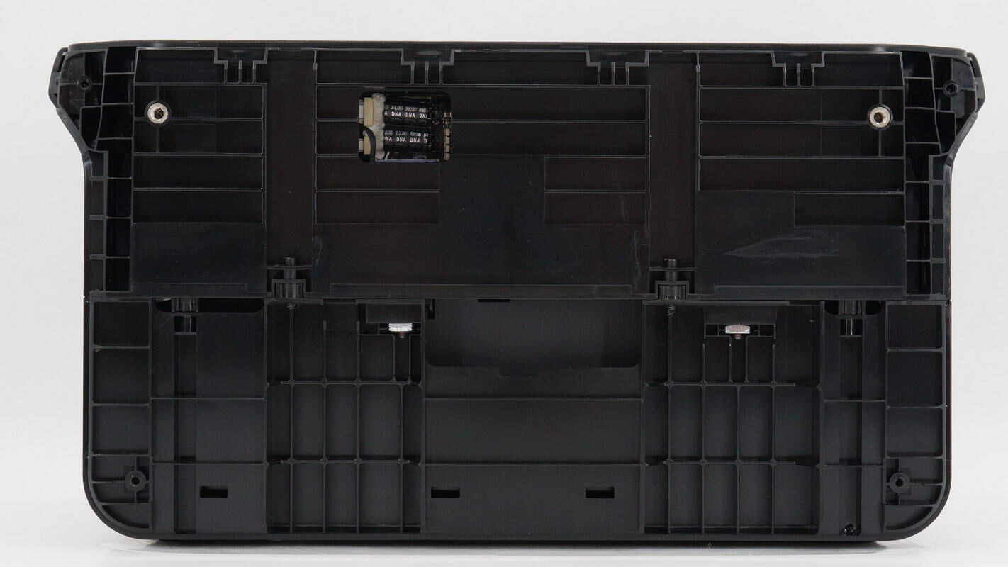
Inside the cover plate, there are reinforcing ribs.
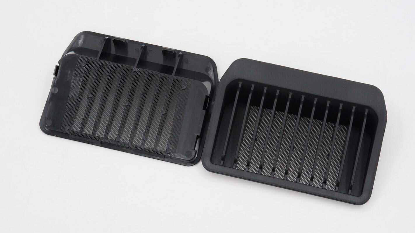
The ventilation grilles on the sides are equipped with filter screens.
The port area uses a gray plastic panel, which is secured with screws.
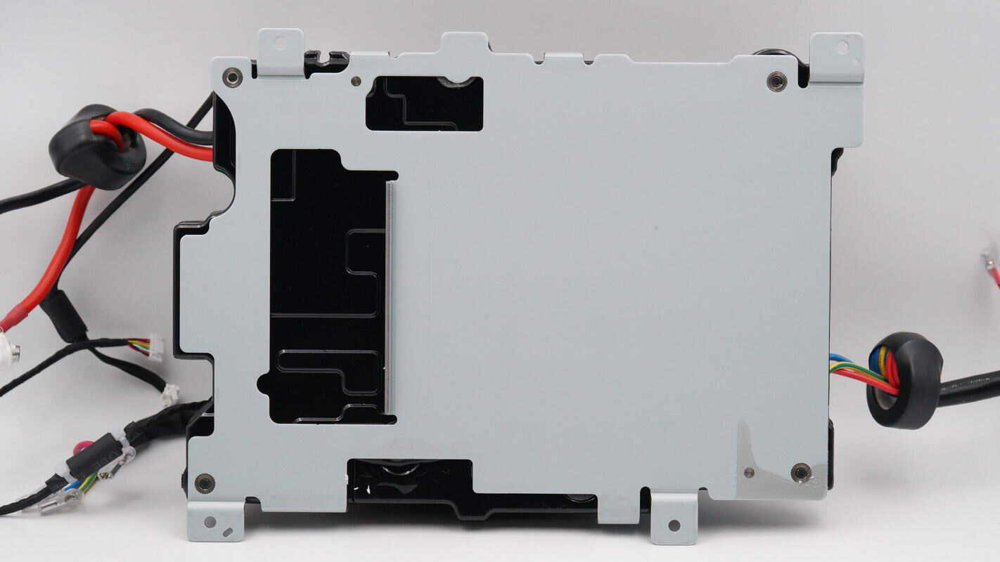
The power station consists of two parts—top and bottom—secured together with screws.
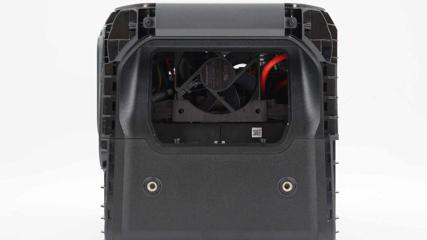
The top cover is secured with screws and houses a cooling fan inside.
There is also a cooling fan on the other side.
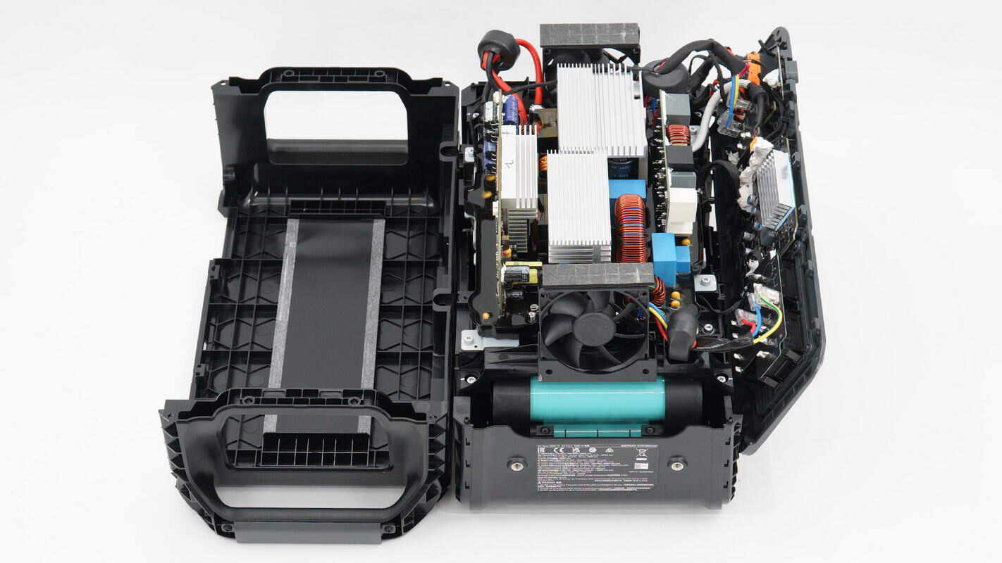
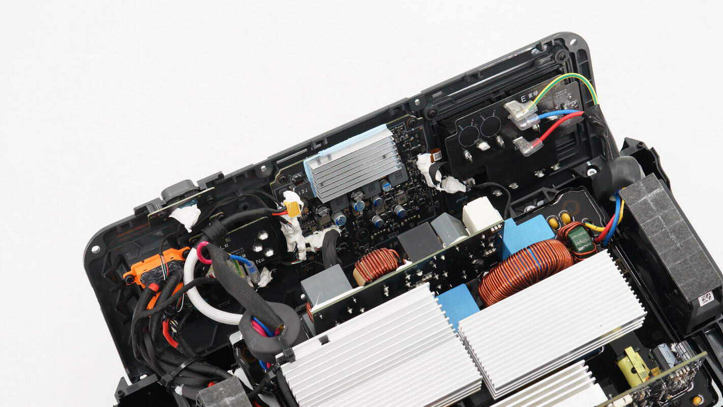
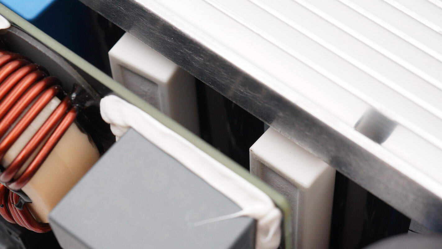
Remove the upper cover, and you will find a bidirectional inverter module inside.
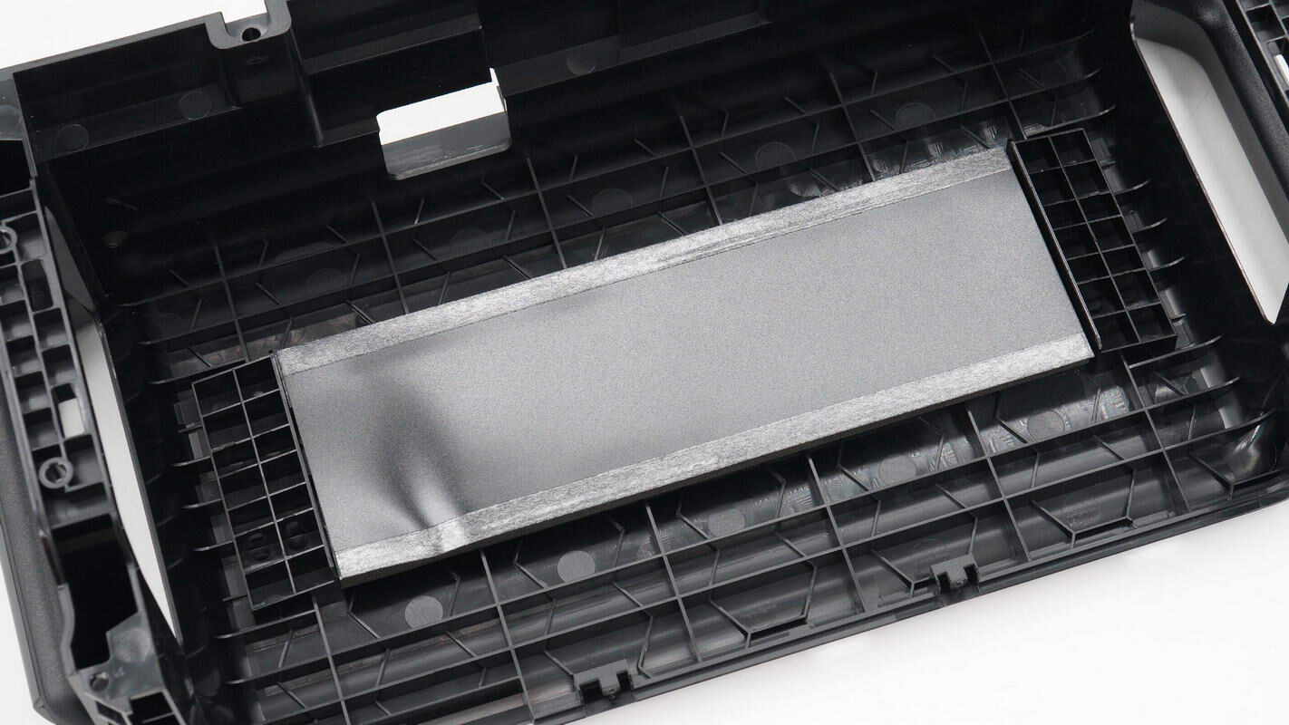
Inside the casing, foam and Mylar sheets are attached to form an air duct, enhancing the cooling performance.
Inside view: the fast charging panel is located at the top, the bidirectional inverter module is in the middle, and cooling fans are positioned on both sides of the inverter module.
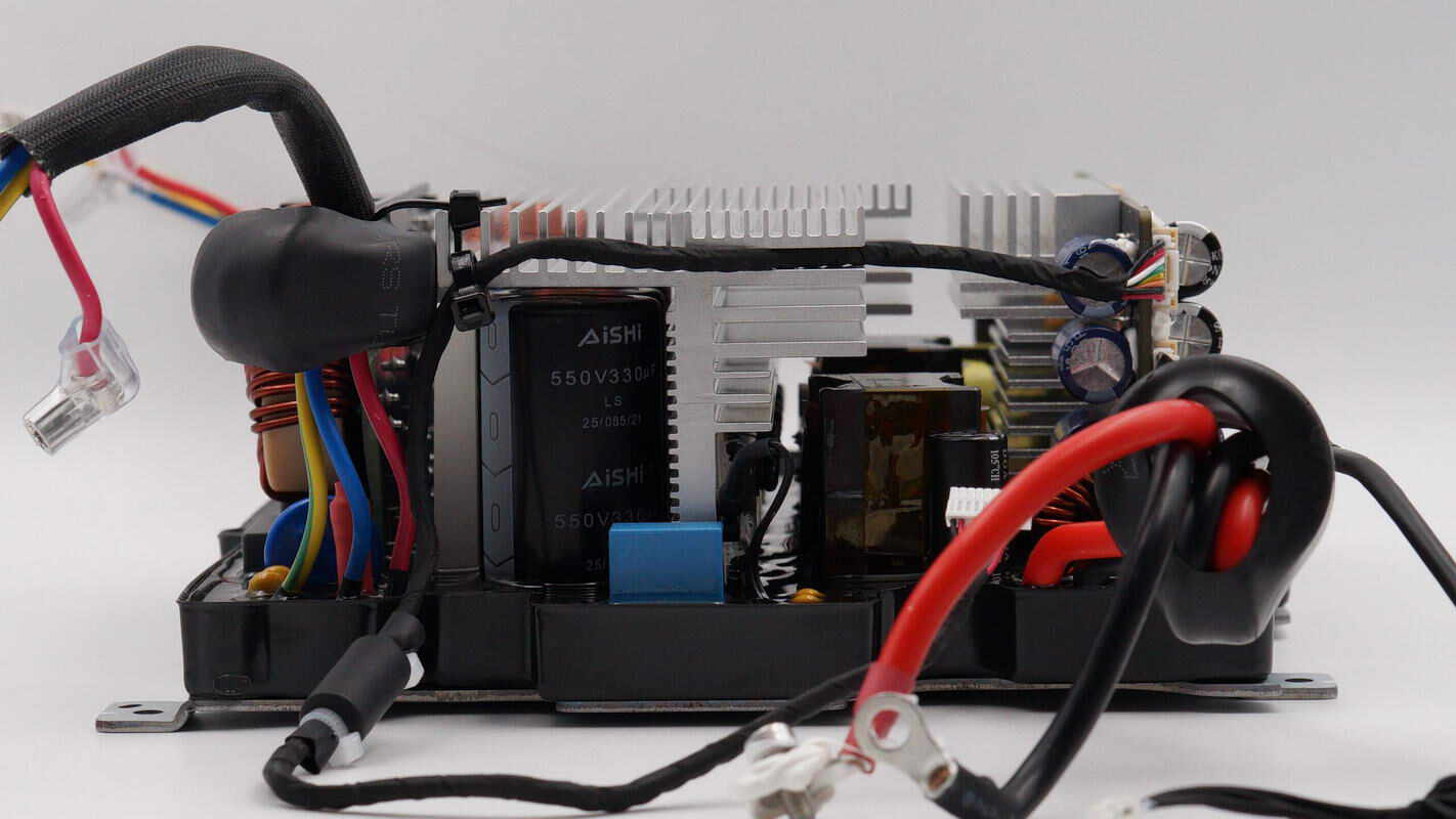
From the side, you can see the control PCB of the bidirectional inverter module.
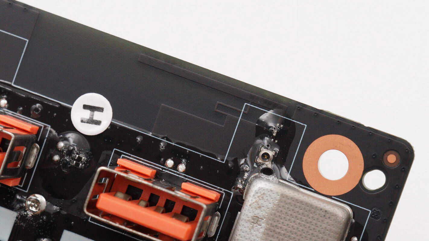
On the side panel, the AC input and output terminals are connected via terminal blocks. The SDC ports are secured with screws and connected with wires. The side panel is powered through an XT30 connector.
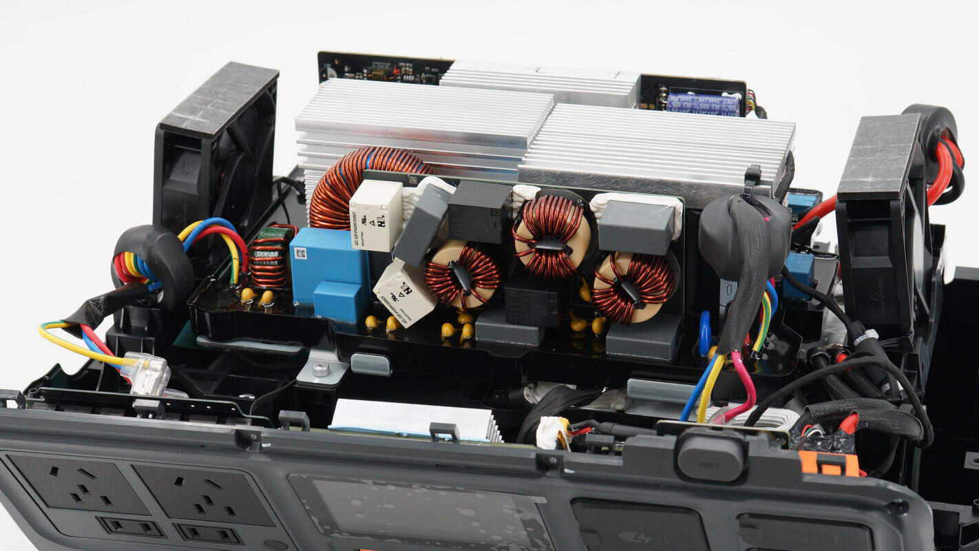
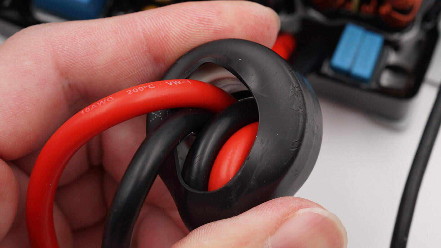
The AC input and output wires are both connected to the bidirectional inverter module.
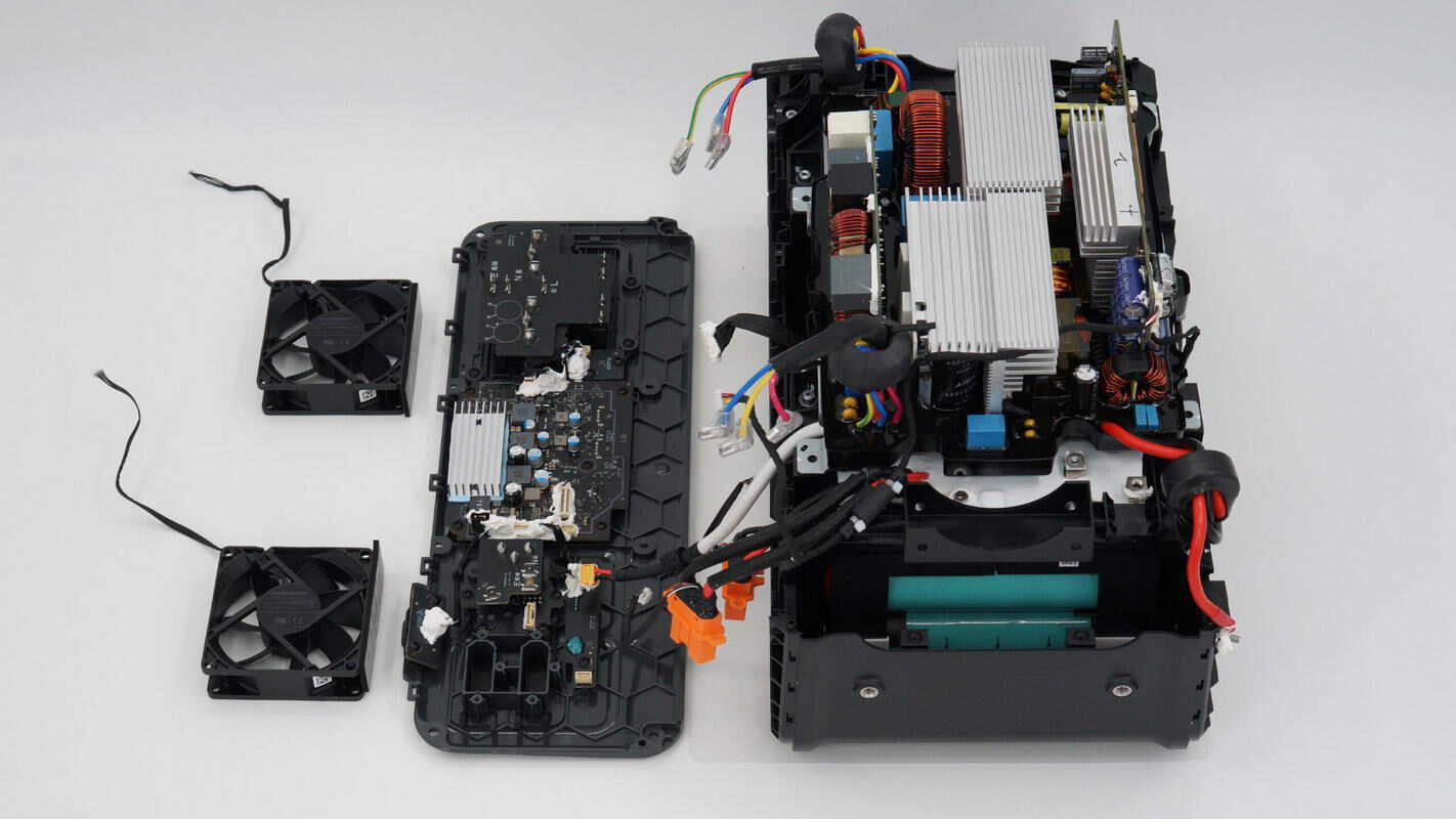
Disconnect the wiring, then remove the cooling fans and the side panel.
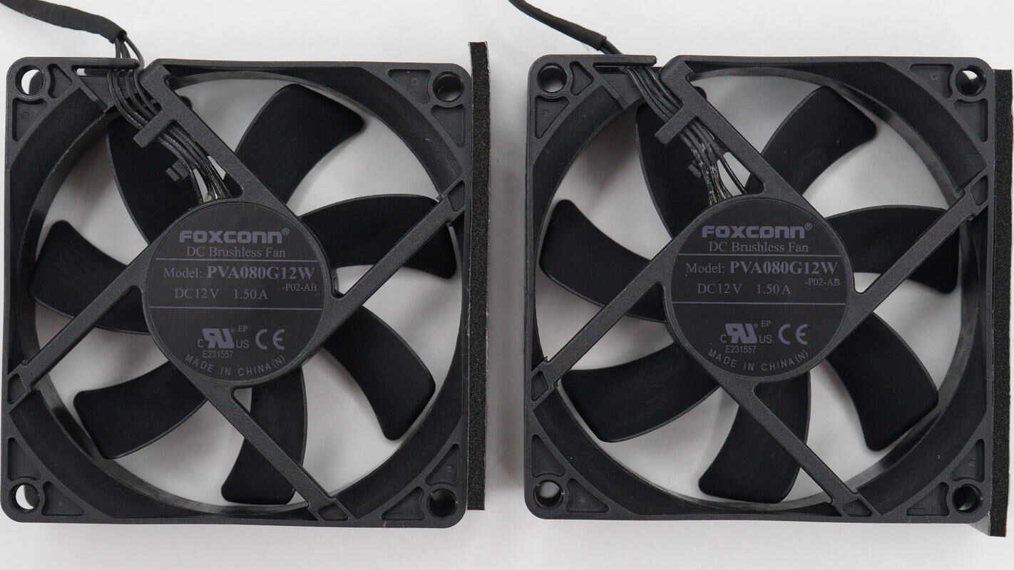
The cooling fans are from Foxconn, model PVA080G12W. They are 80x80x12mm in size, rated at 12V 1.5A, and feature four-wire temperature control.
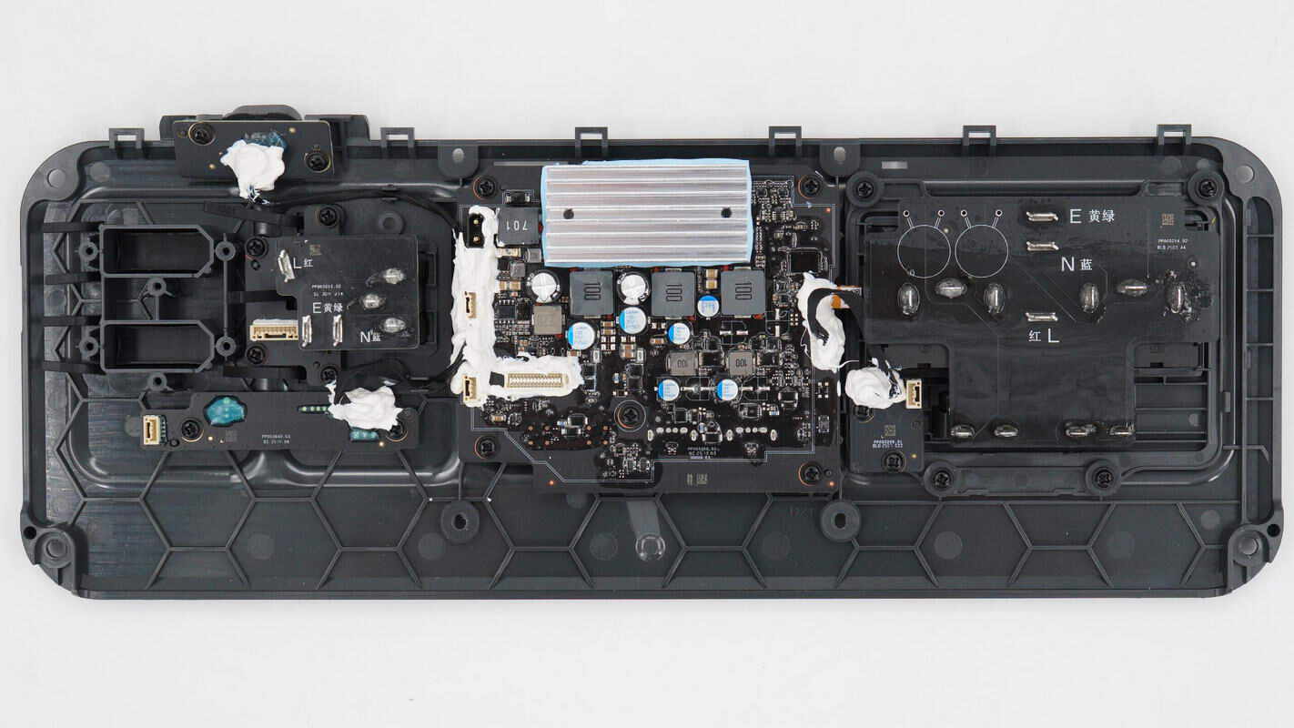
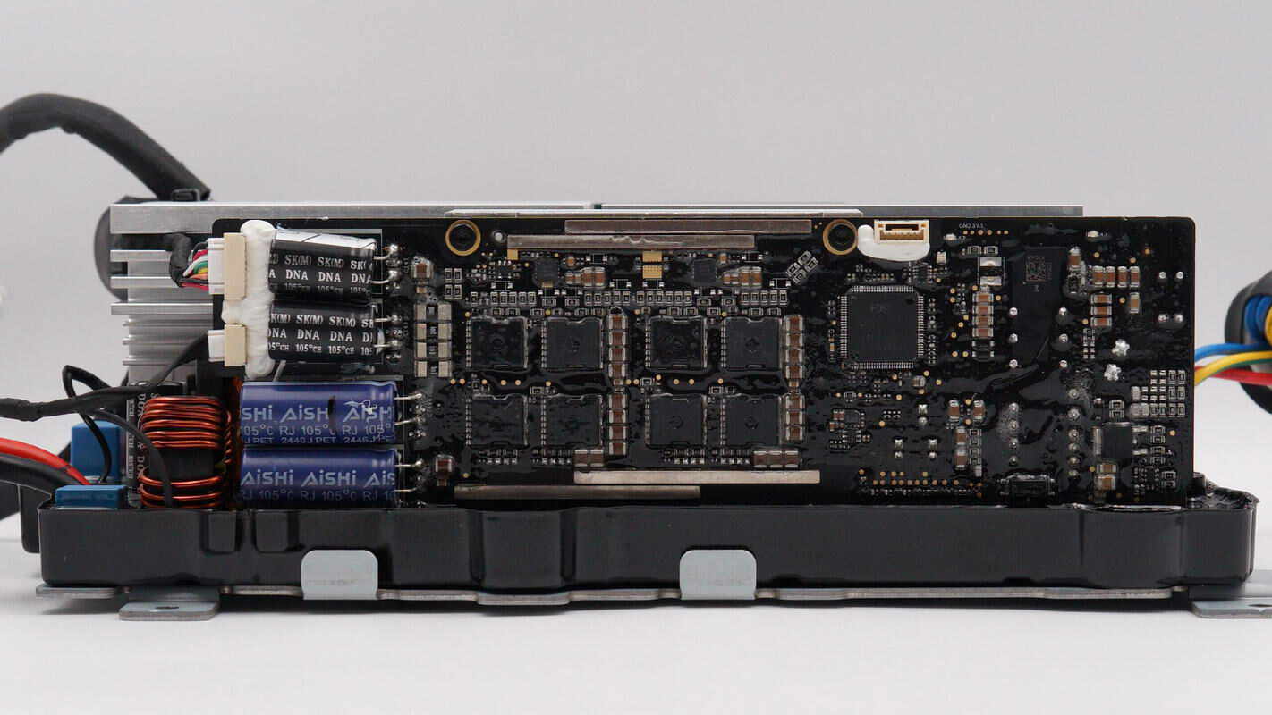
On the inner side of the panel, there is a PCBA module responsible for USB fast charging output and screen control.
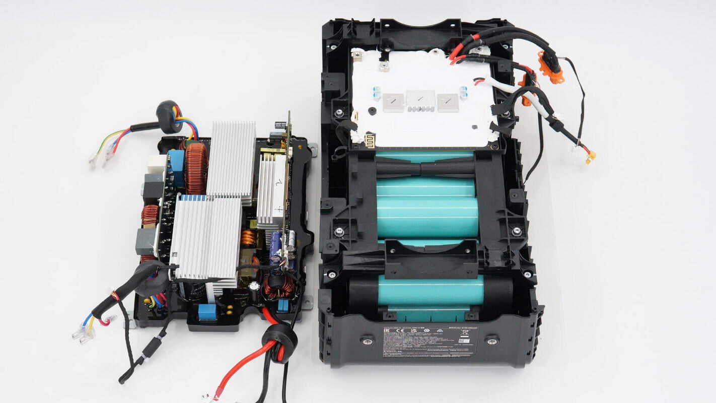
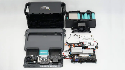
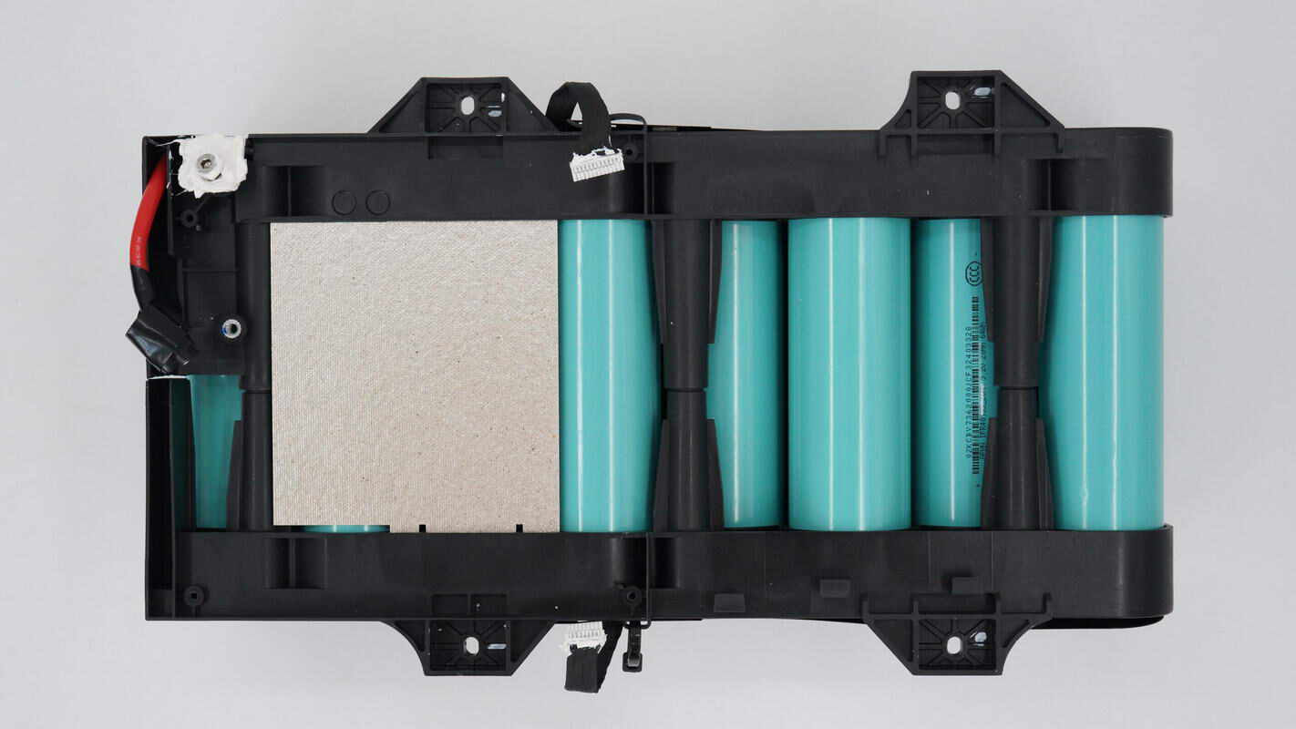
After removing the bidirectional inverter module, the battery pack is located directly beneath it.
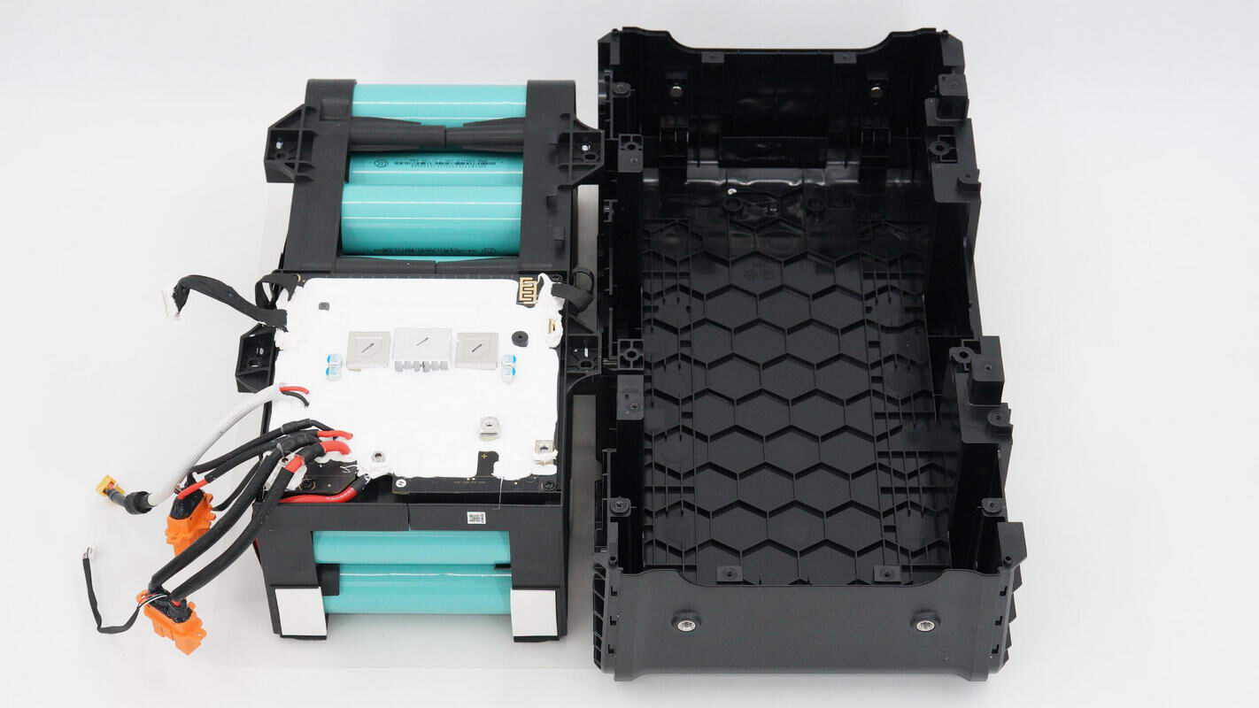
After removing the battery pack, you can see that the interior of the casing features reinforcing rib structures.
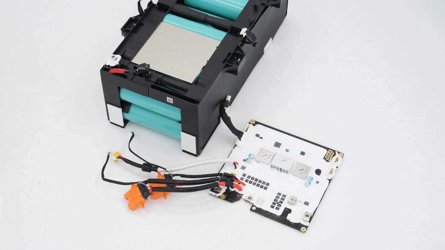
Unscrew the screws and remove the protective PCB of the battery pack.
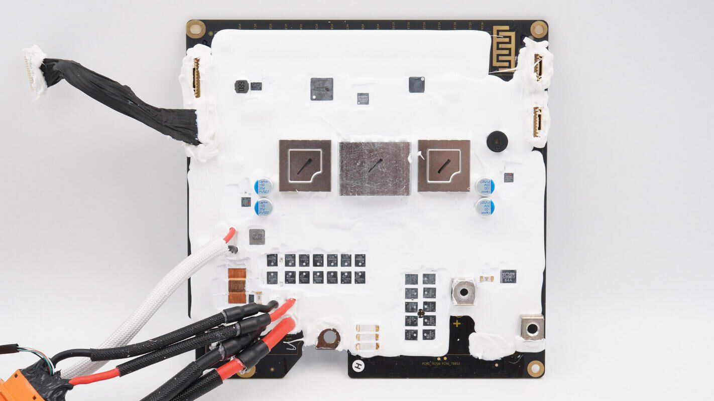
The protective PCB is fully coated with potting compound for sealing. In the center, there is a heatsink along with an alloy inductor and filter capacitors. Above that are the MCU and battery protection chip. Below are the fuse, battery protection transistor, and sampling resistor. In the lower right corner, a terminal post connects to the bidirectional inverter module.
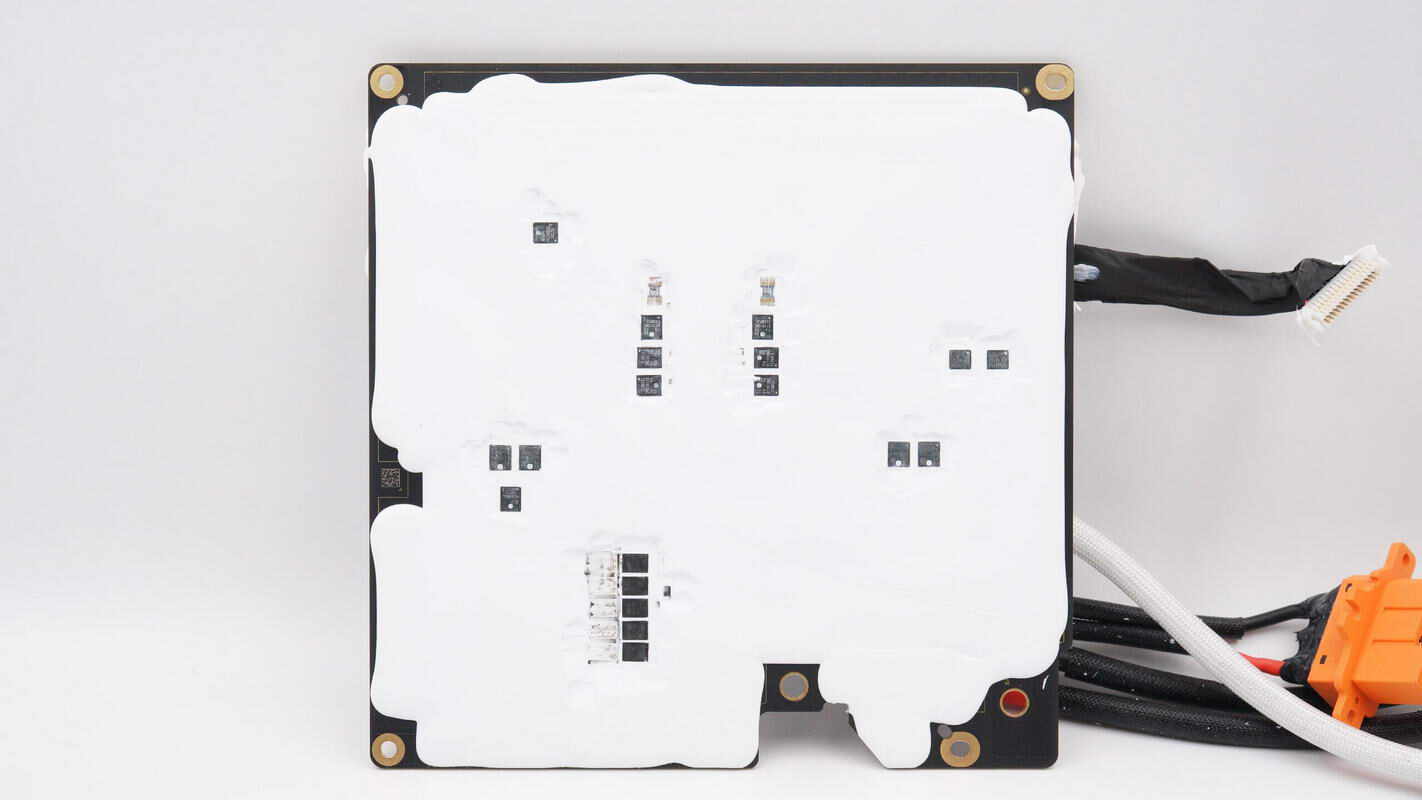
On the back side, there are MOSFETs and diodes.
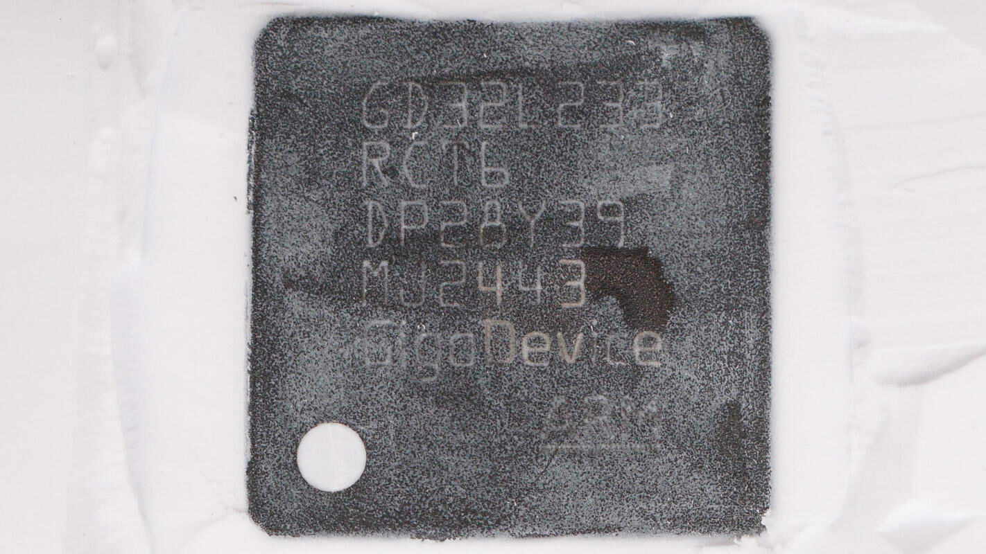
The MCU is from GigaDevice, model GD32L233RCT6. It features a Cortex-M23 core, is a low-power 32-bit processor with 256KB of flash memory and 32KB of SRAM. It includes two UART interfaces, two USART interfaces, one LPUART interface, three I2C interfaces, two SPI interfaces, and one I2S interface. The chip comes in an LQFP64 package.
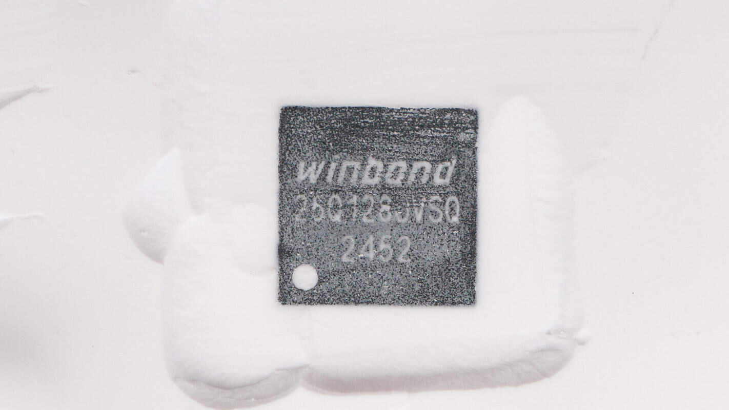
The memory chip is from Winbond, model W25Q128JVSIQ, with a capacity of 16MB. It comes in an SOP8 package.
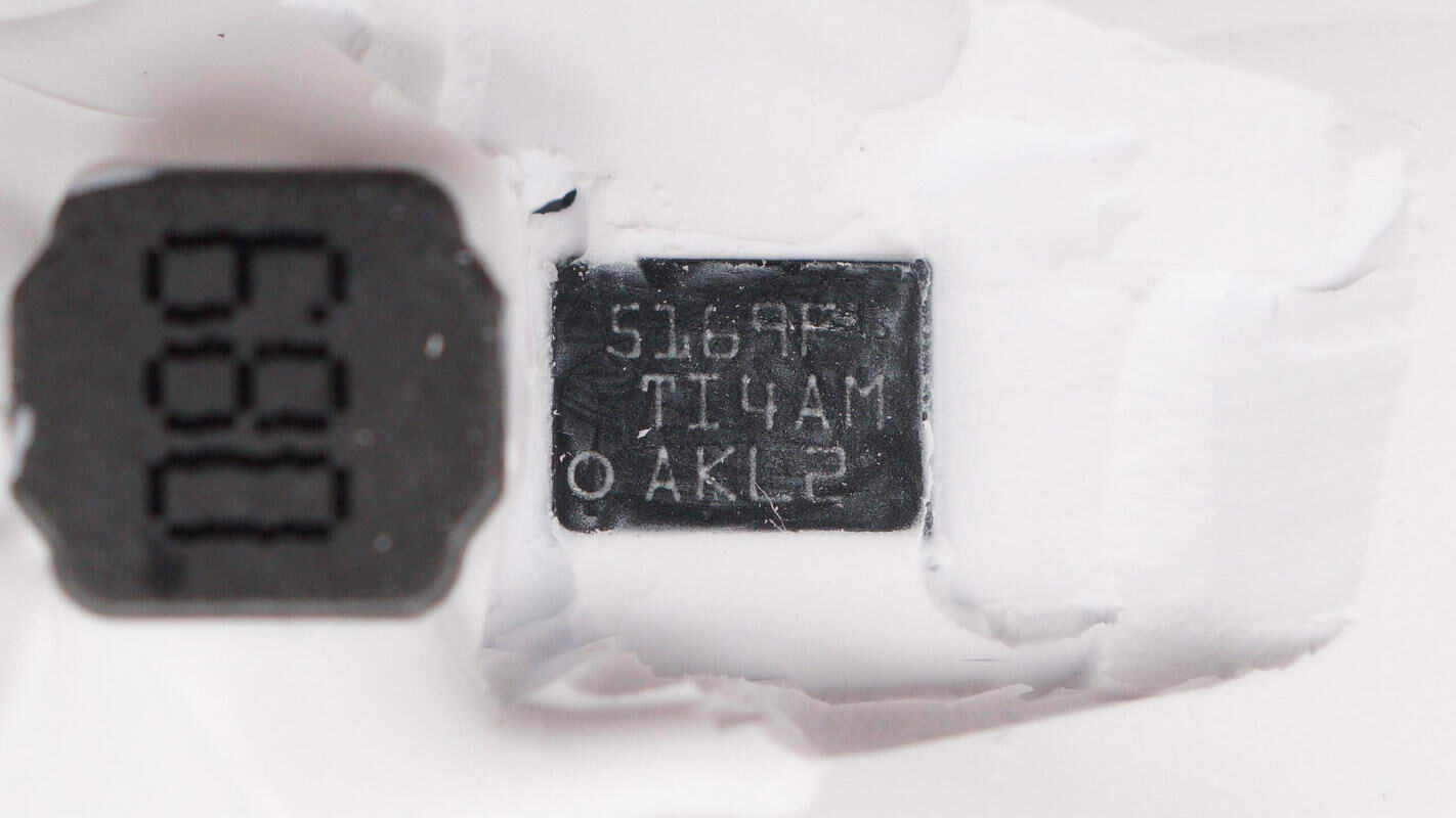
The buck chip comes from TI, marked with 5169F, model LM5169. It is a synchronous buck converter supporting up to 120V input voltage. The chip has an internal MOSFET and supports 0.65A output current. It uses an HSOIC8 package.
The buck chip is from TI, marked with 5169F, model LM5169. It is a synchronous buck converter supporting up to 120V input voltage. The chip has built-in MOSFETs and supports an output current of 0.65A. It comes in an HSOIC8 package.
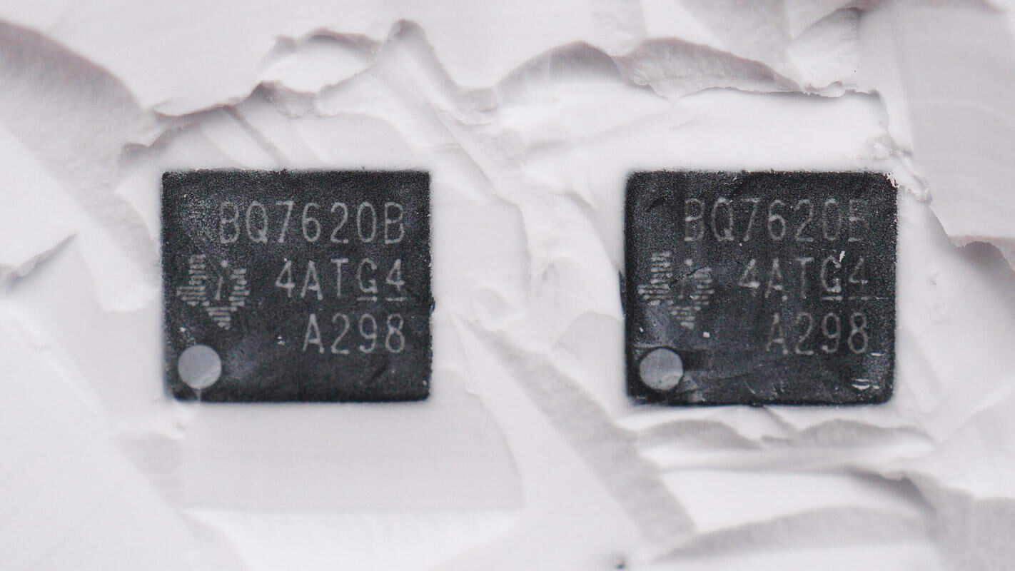
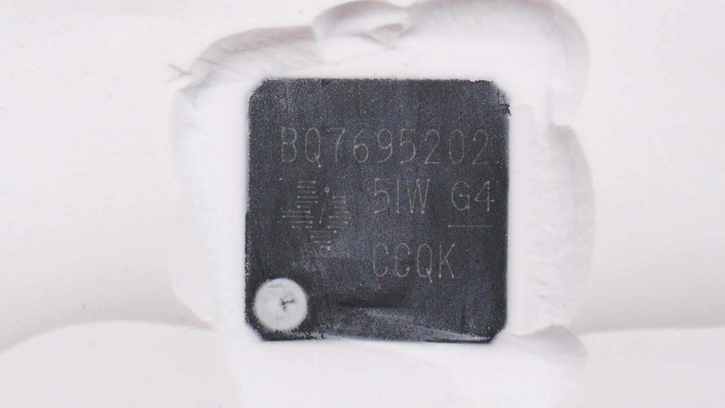
The MOSFET driver is from TI, model BQ76200. It is used to drive the battery protection transistor and comes in a TSSOP16 package.
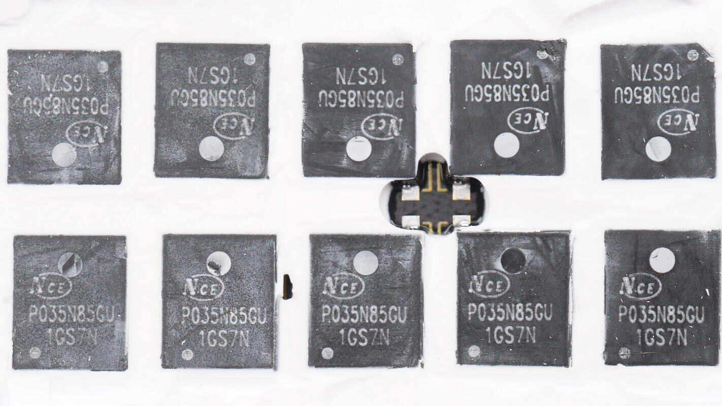
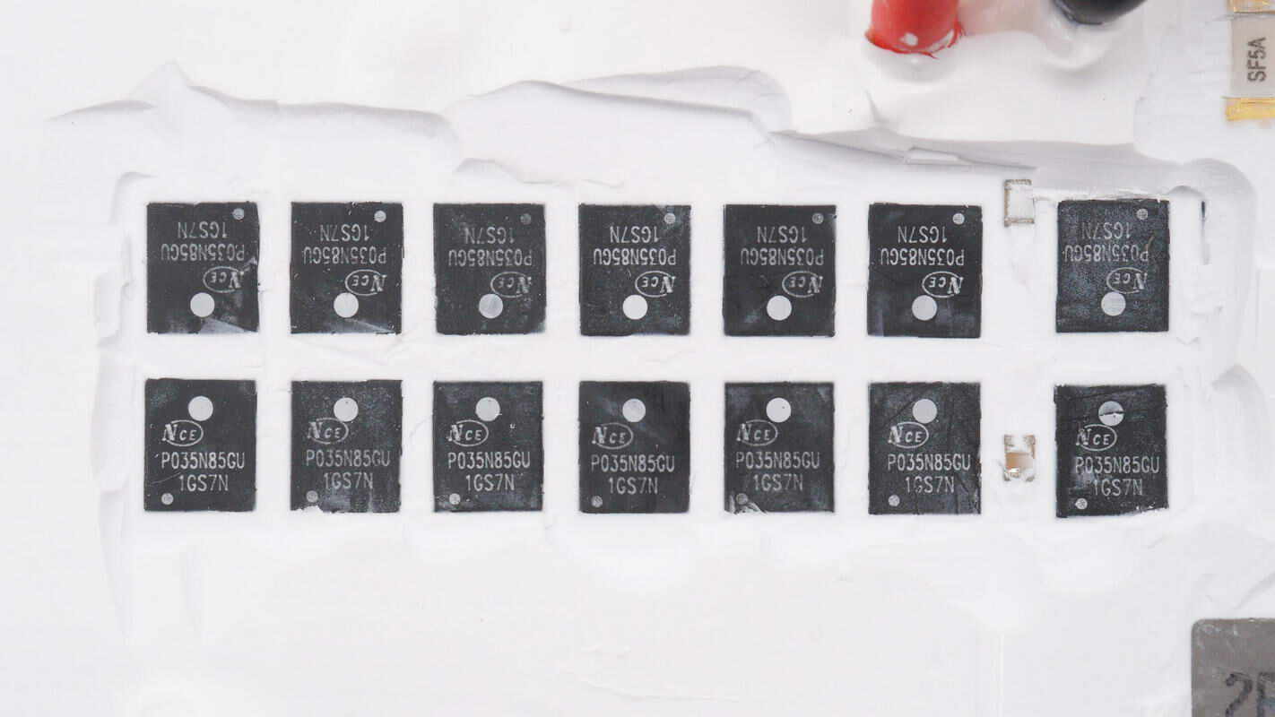
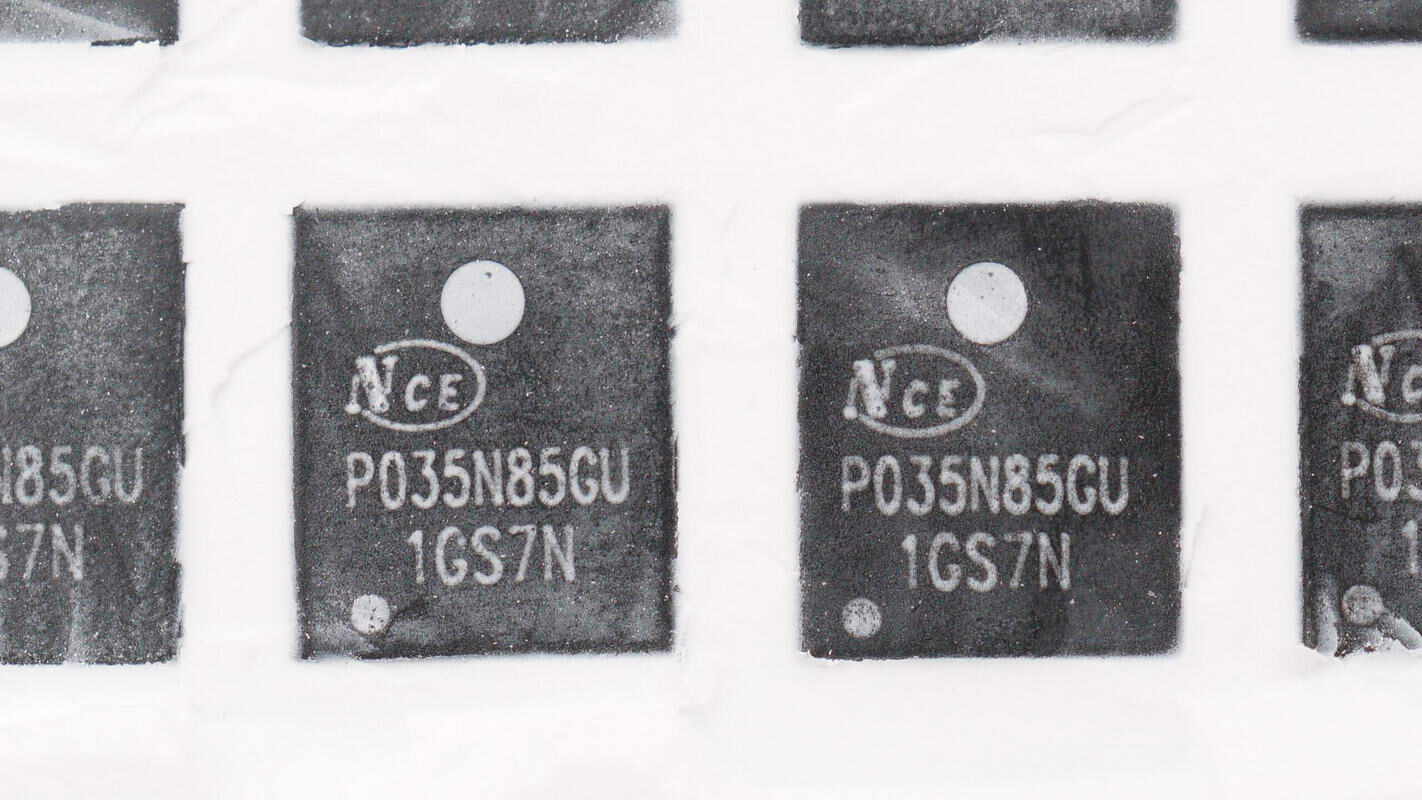
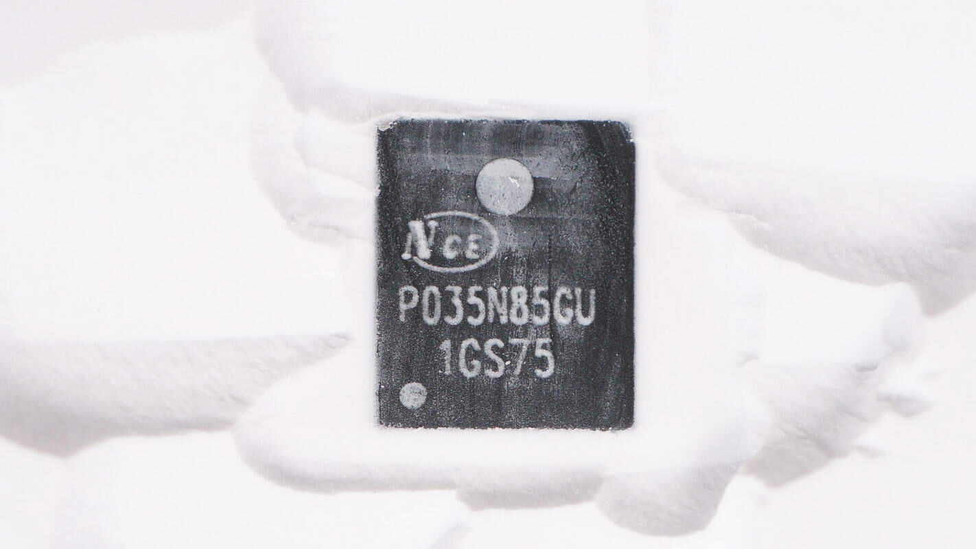
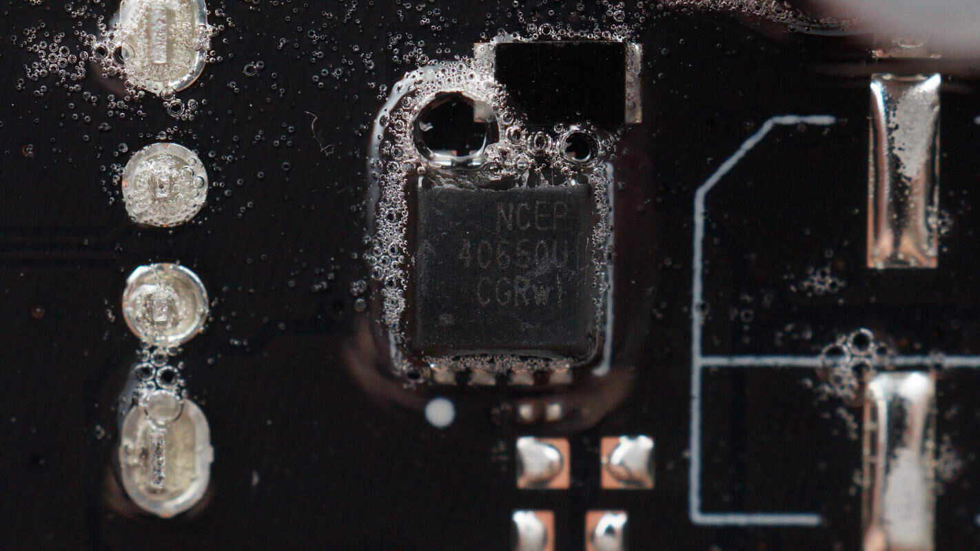
The battery protection transistors are from NCE, model NCEP035N85GU. It is an NMOS with an 85V voltage rating and a low on-resistance of 2.9mΩ, packaged in a DFN 5×6 mm form factor.
There are Schottky diodes soldered on the back side of the battery protection transistors.
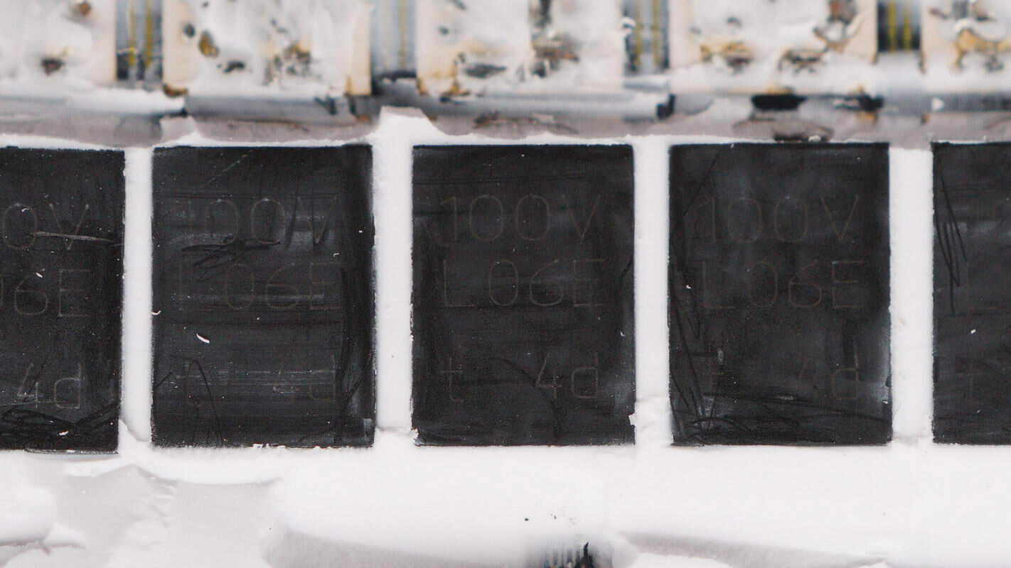
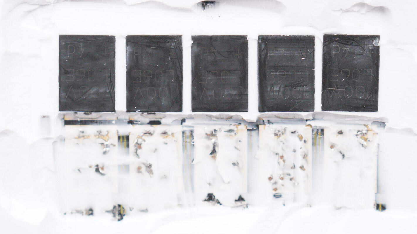
The Schottky diodes are from Nexperia, marked with 100V L06E, model PMEG100V060ELPD. They are rated for 100V and 6A, and come in SOT1289 packages.
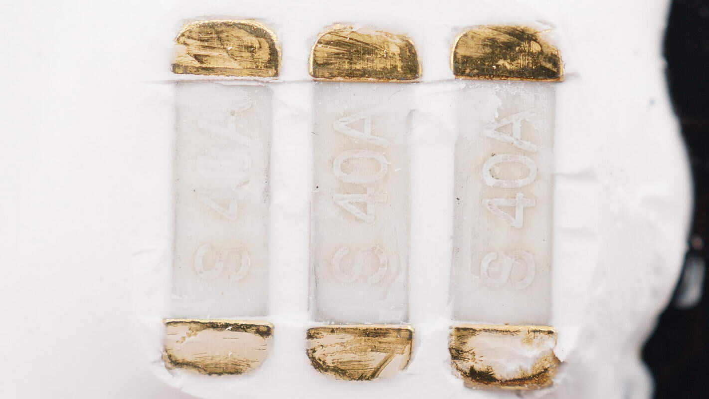
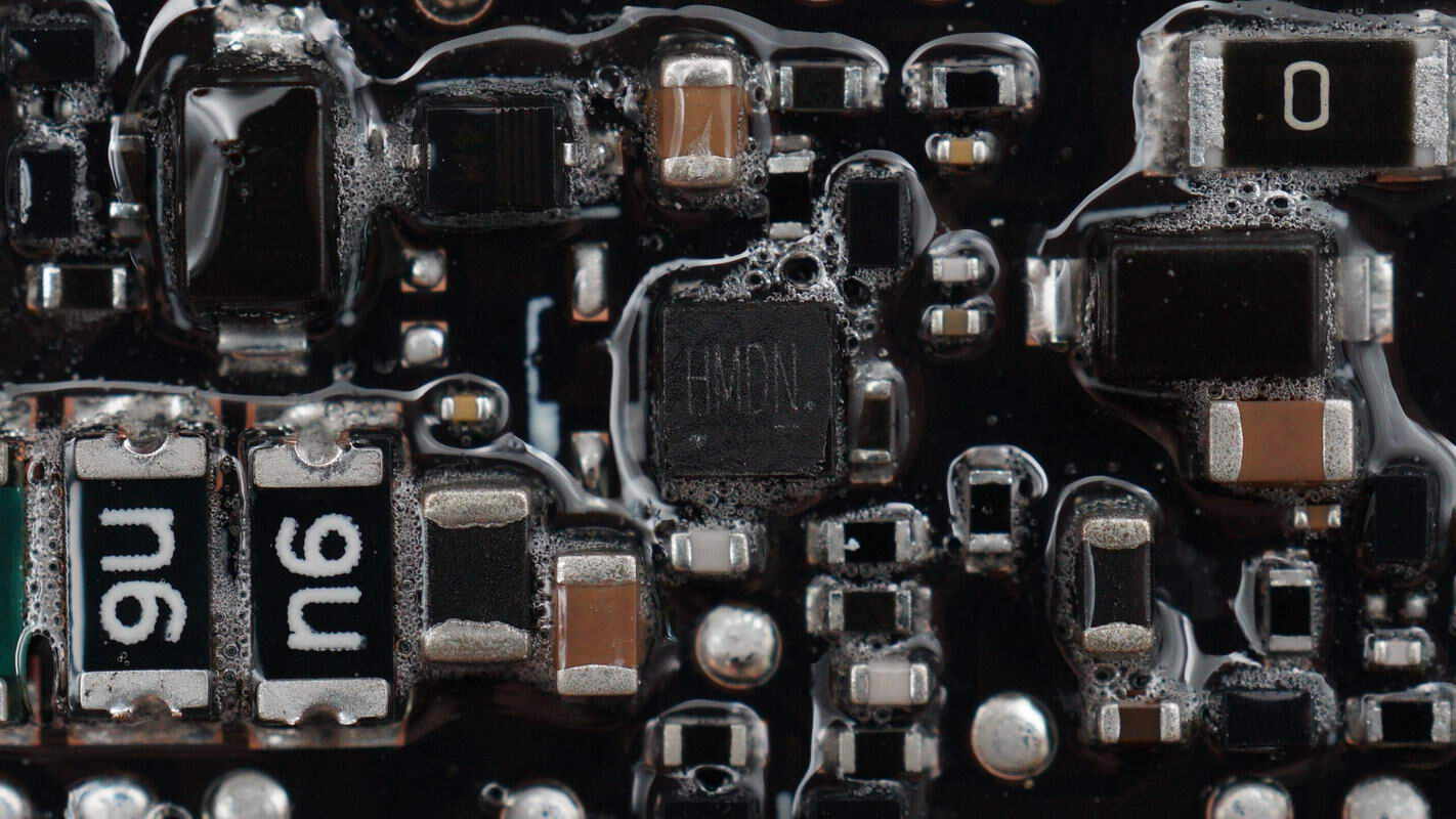
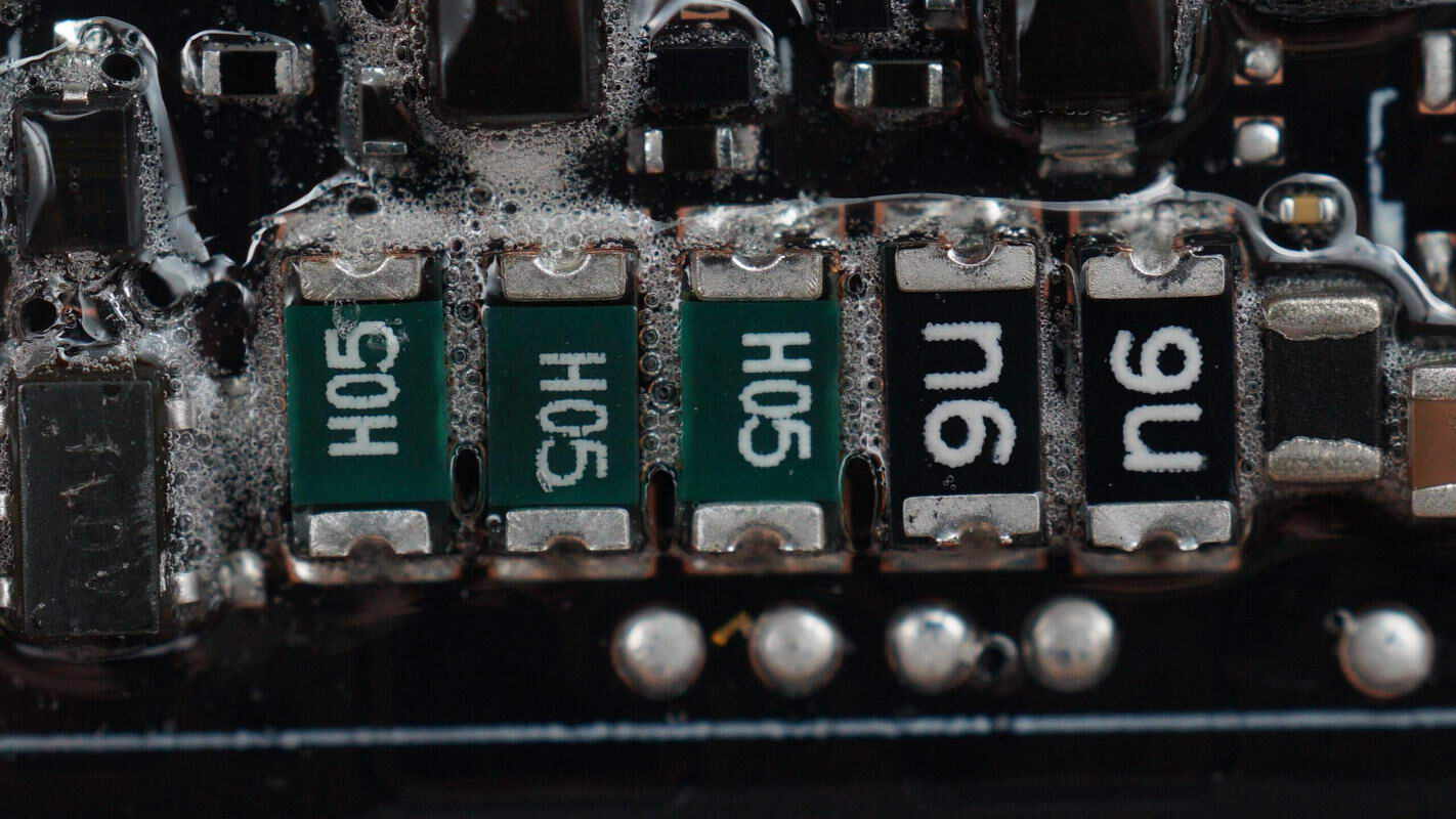
Three 40A fuses are connected in parallel for overcurrent protection of the battery pack.
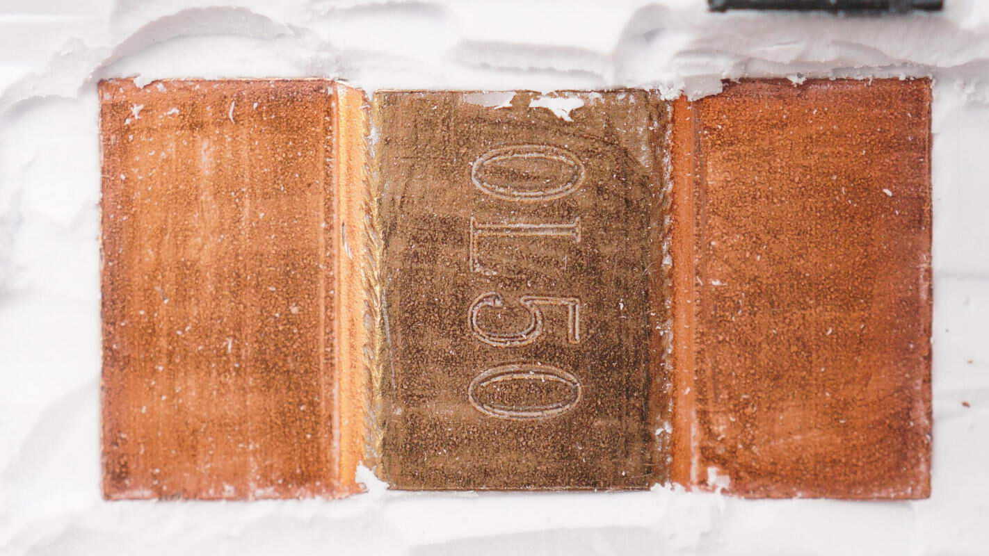
A 0.5mΩ sampling resistor is used for current sensing in the battery pack.
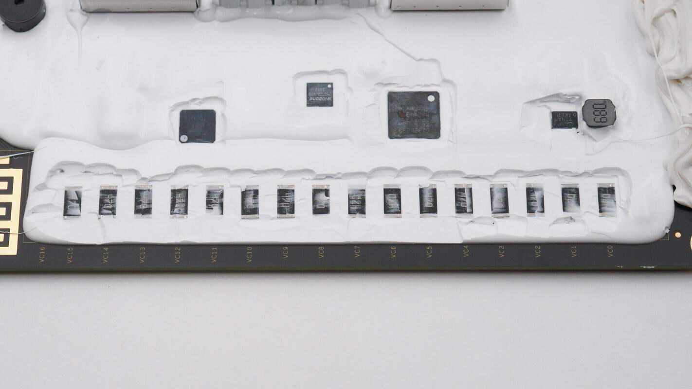
Close-up of the resistors used for series battery pack balancing.
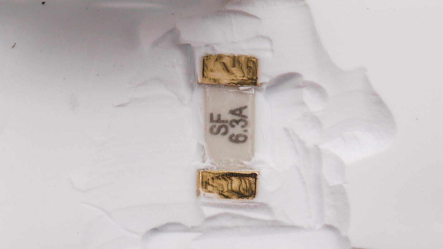
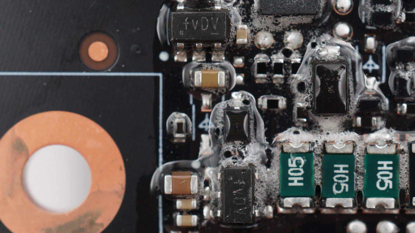
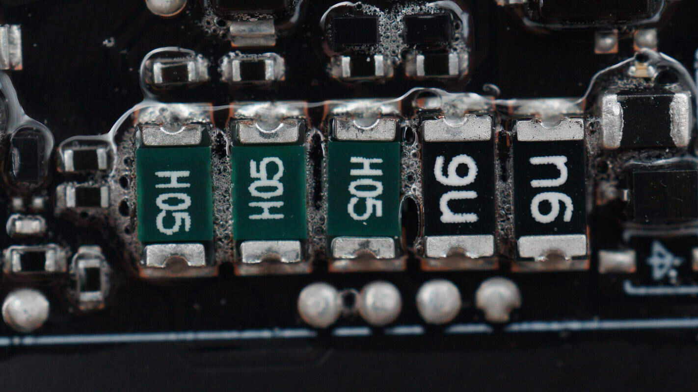
At the output end of the protection PCB, there are fuses and TVS diodes. The SMD fuse is rated at 6.3A.
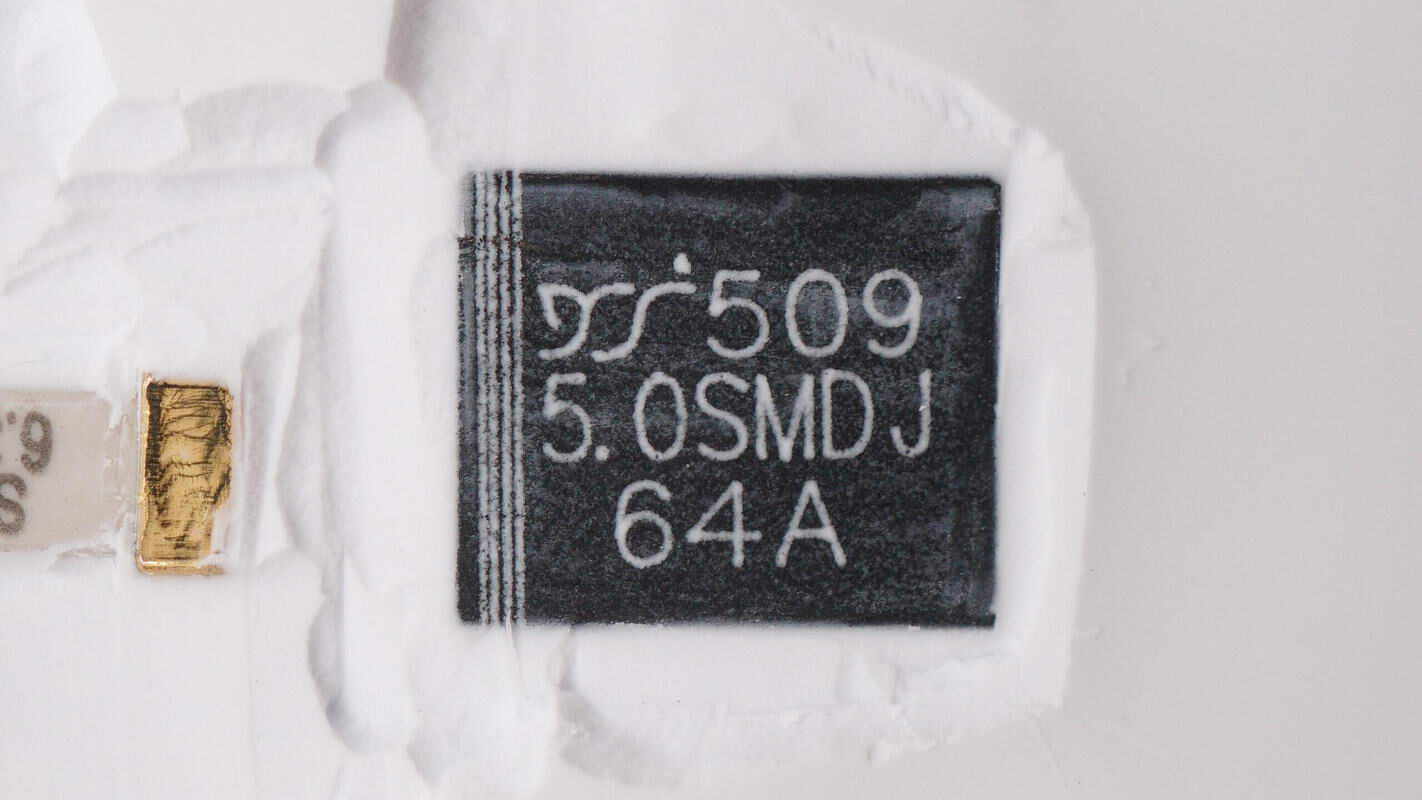
The TVS diode is from YJ, model 5.0SMDJ64A, with an operating voltage of 64V. It is used to absorb overvoltage surges at the output and comes in an SMC package.
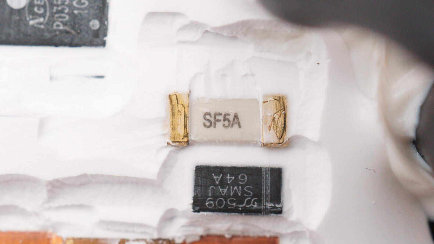
Another set of fuse and TVS diode is used for overvoltage protection of the SDC interface. The SMD fuse is rated at 5A.
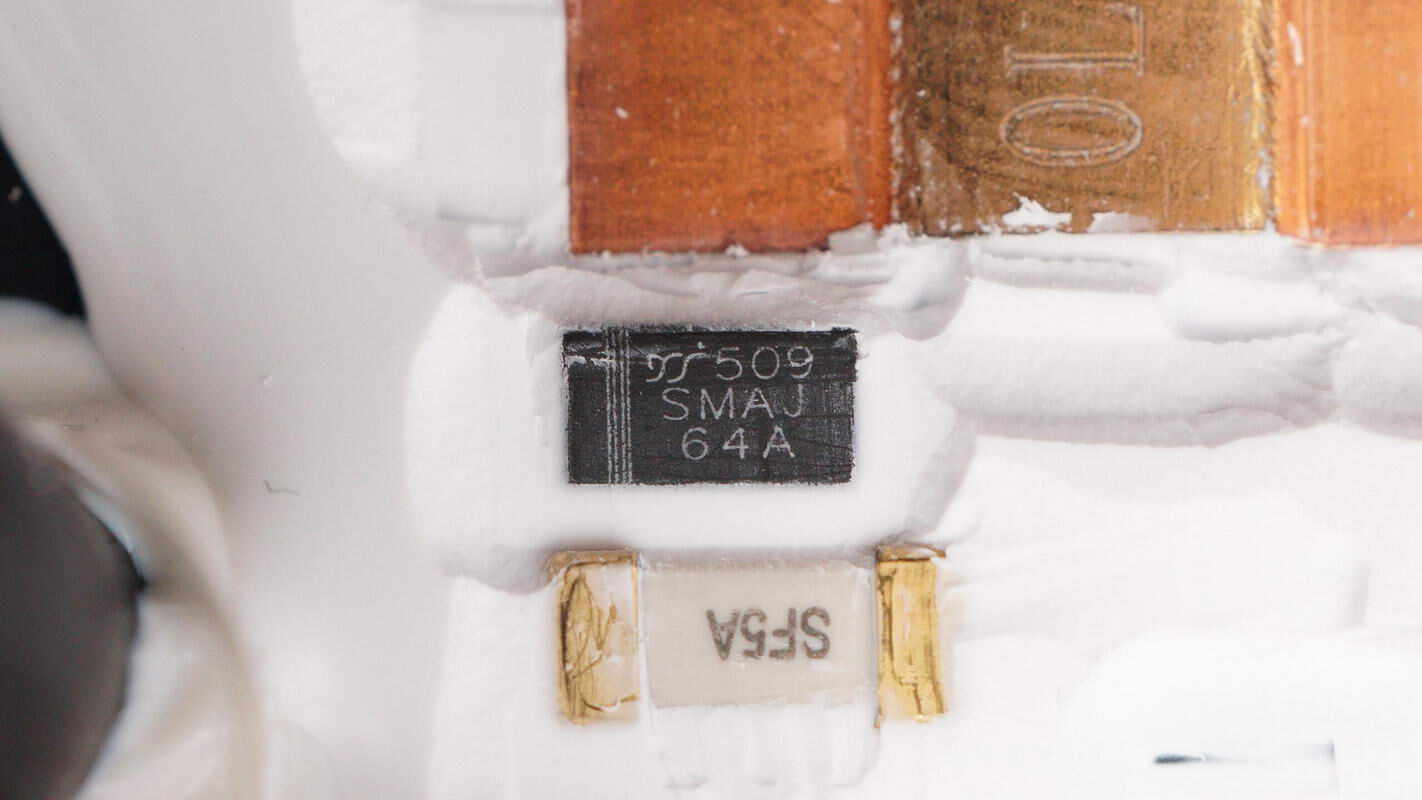
The TVS diode is from YJ, model 5.0SMAJ64A, with an operating voltage of 64V. It is used to absorb overvoltage surges at the output and comes in an SMA package.
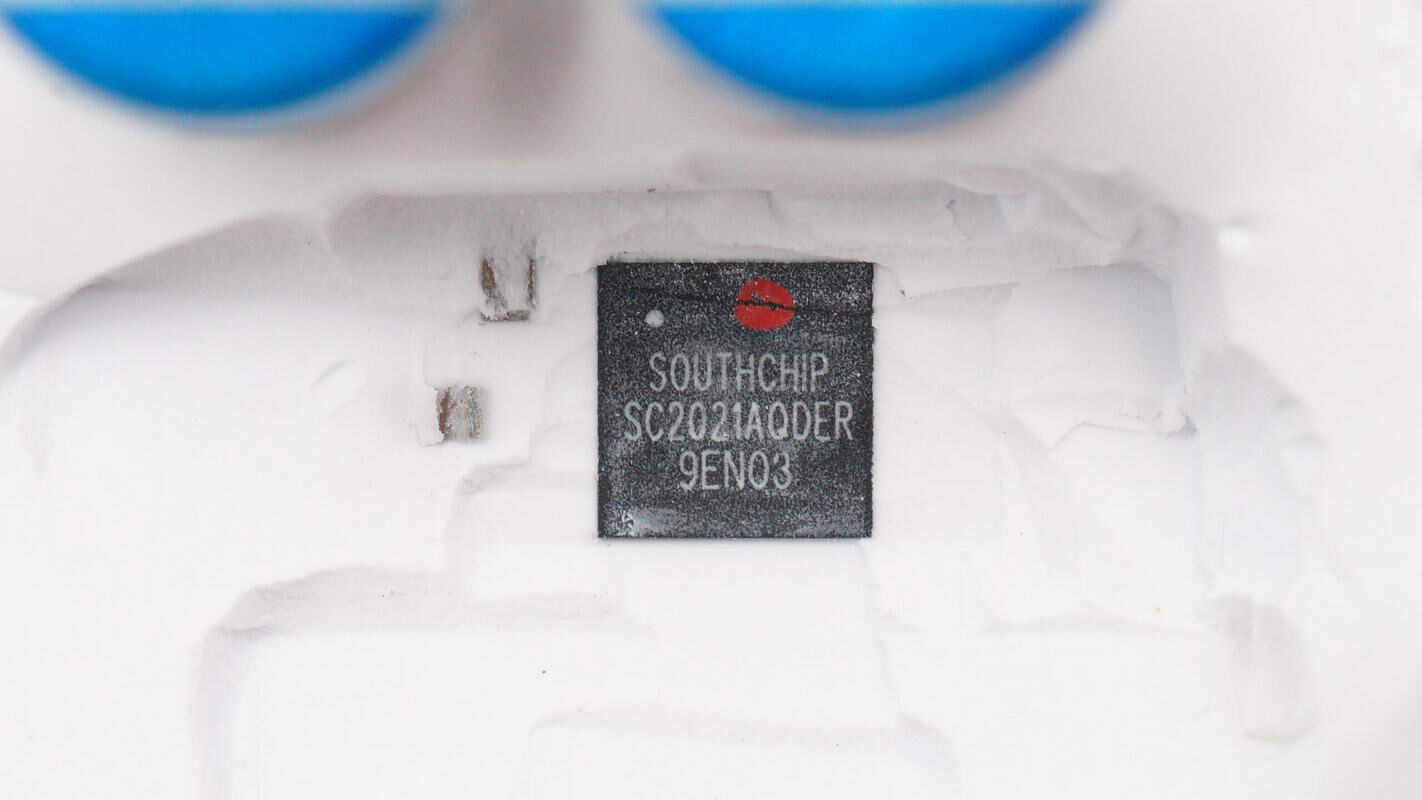
The two protocol chips are from SouthChip, model SC2021A. They are highly integrated Type-C/PD and DPDM fast charging controllers that comply with the latest Type-C and PD 3.0 standards and have passed USB PD 3.1 compliance testing. These chips support proprietary high-voltage fast charging protocols and feature one set of USB-C interfaces plus two sets of DPDM interfaces, enabling dual-port fast charging with one USB-A and one USB-C port. They come in QFN32 packages.
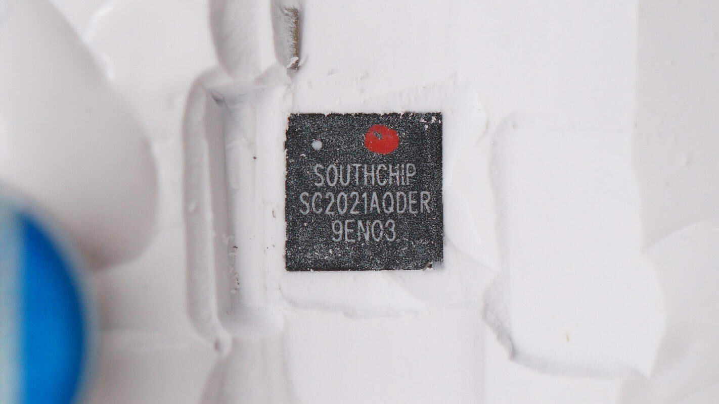
Close-up of the other SouthChip SC2021A chip.
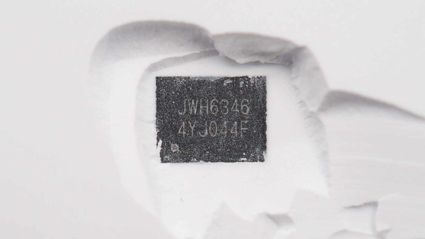
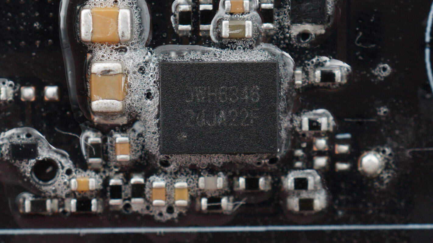
The synchronous buck controller used alongside is from JOULWATT, model JWH6346. It supports up to 100V input voltage when powered externally via VCC, and up to 75V input voltage when powered internally via VCC. It supports a 60V output voltage and operates at a switching frequency range of 100kHz to 1MHz. The chip features a synchronization signal pin, built-in overcurrent protection, undervoltage protection, and provides a PG signal output.
Here is the information about JOULWATT JWH6346.
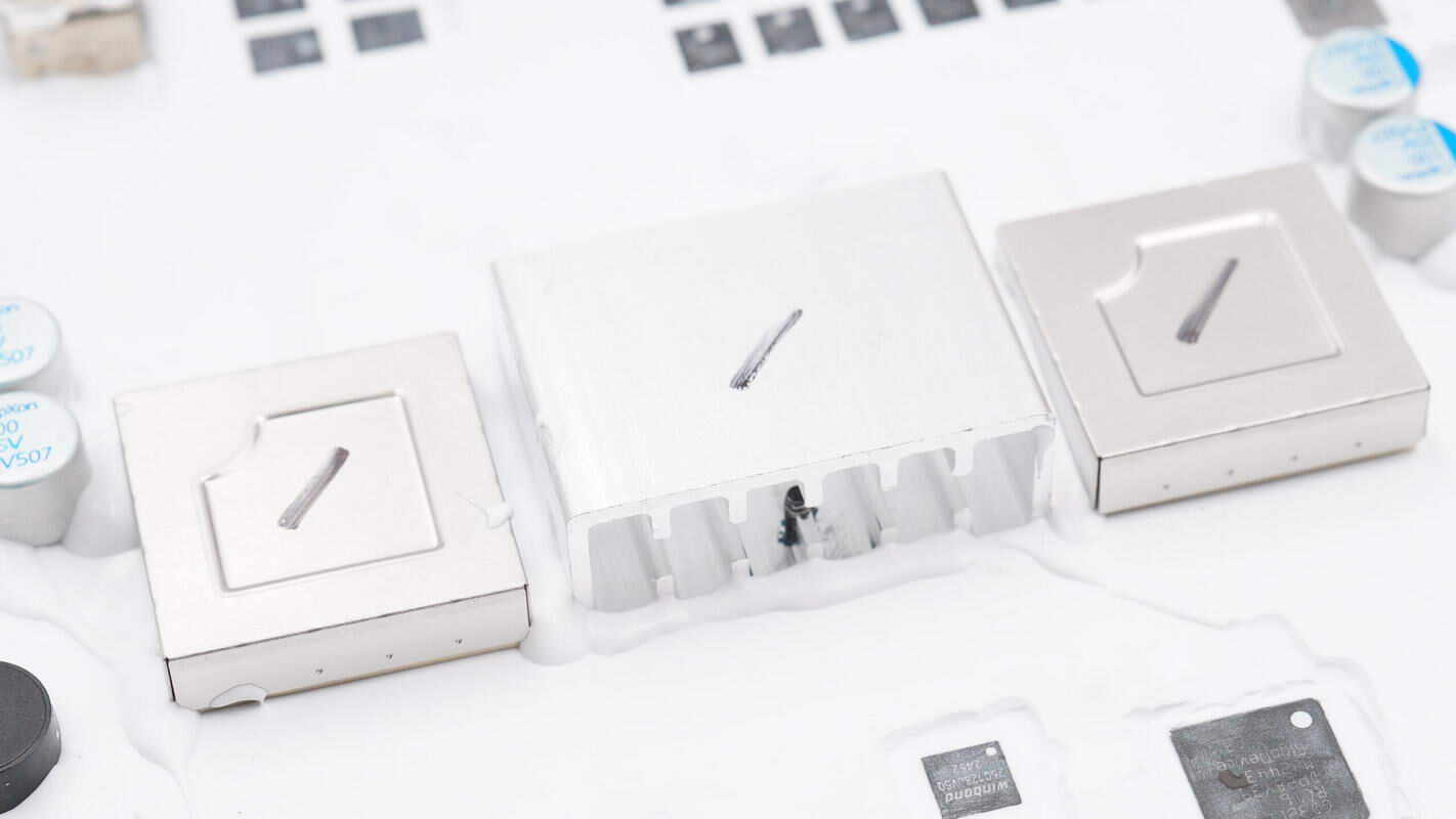
Two power inductors are equipped with shielding covers, with a heatsink positioned between them.

Thermal gel is applied between the inductors and their shielding covers to enhance heat dissipation.
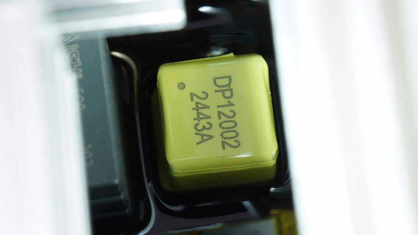
The alloy inductor has a specification of 10μH.
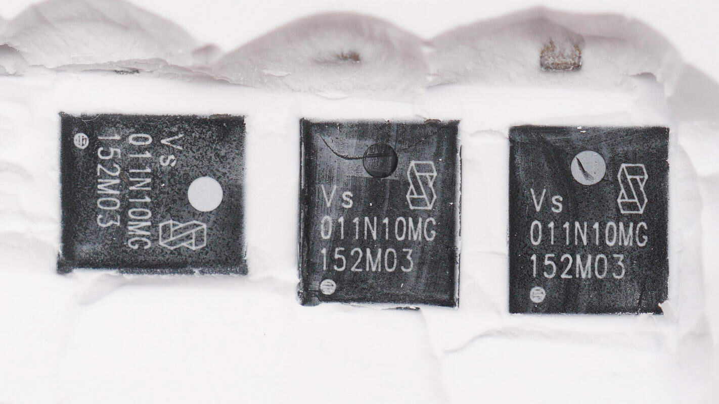
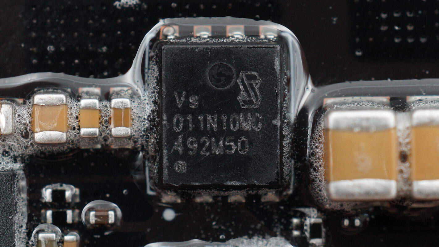
The synchronous buck MOSFET is from Vergiga, model VSP011N10MS-G. It is an NMOS transistor with a 100V voltage rating and an on-resistance of 9.5mΩ, packaged in a PDFN 5×6 mm form factor.
Here is the information about Vergiga VSP011N10MS-G.
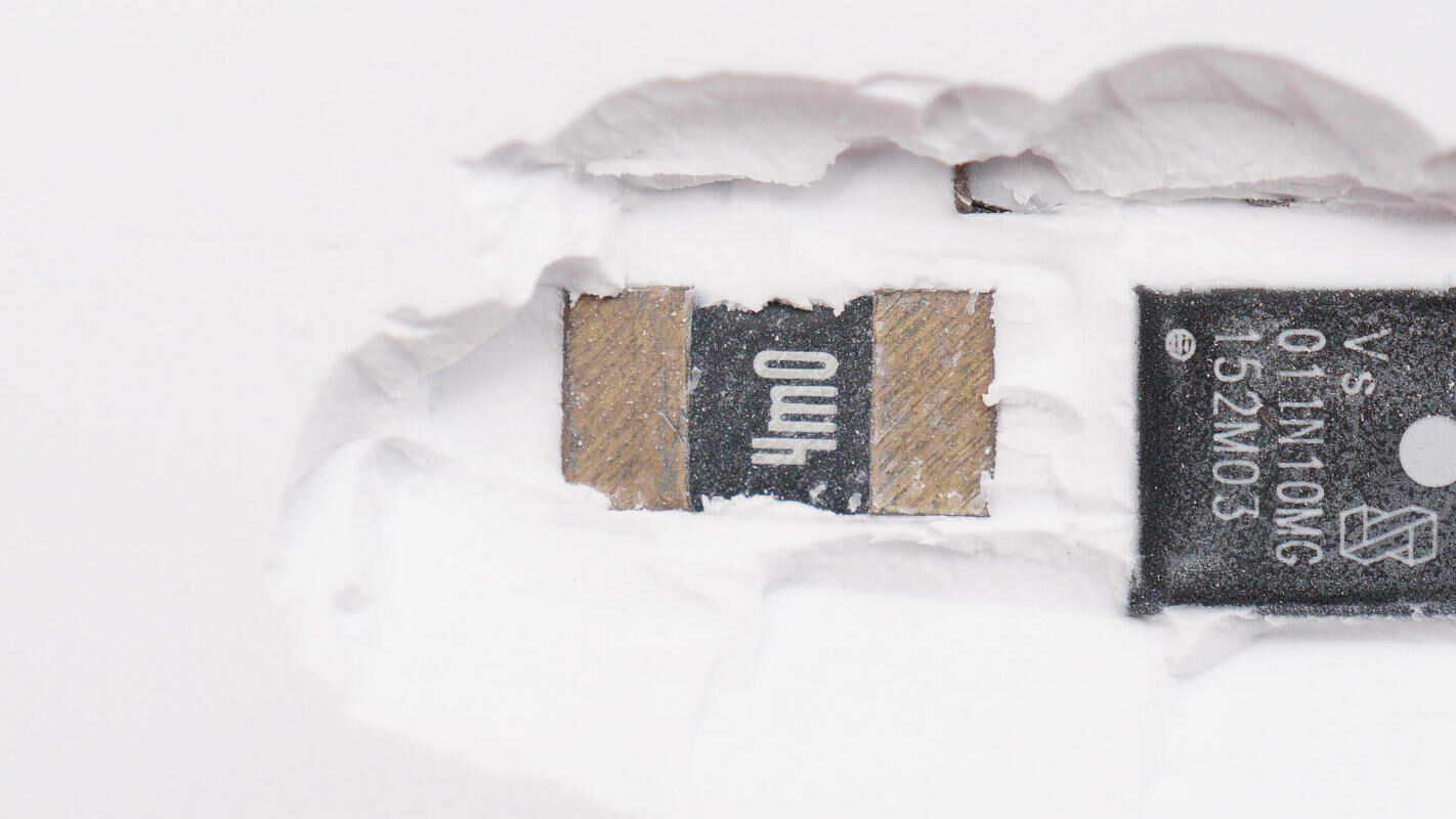
Close-up of the 4mΩ current sampling resistor.
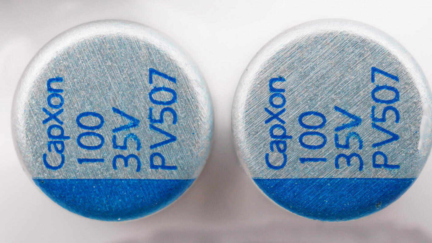
The two filter capacitors are from CapXon, each rated at 100μF and 35V.
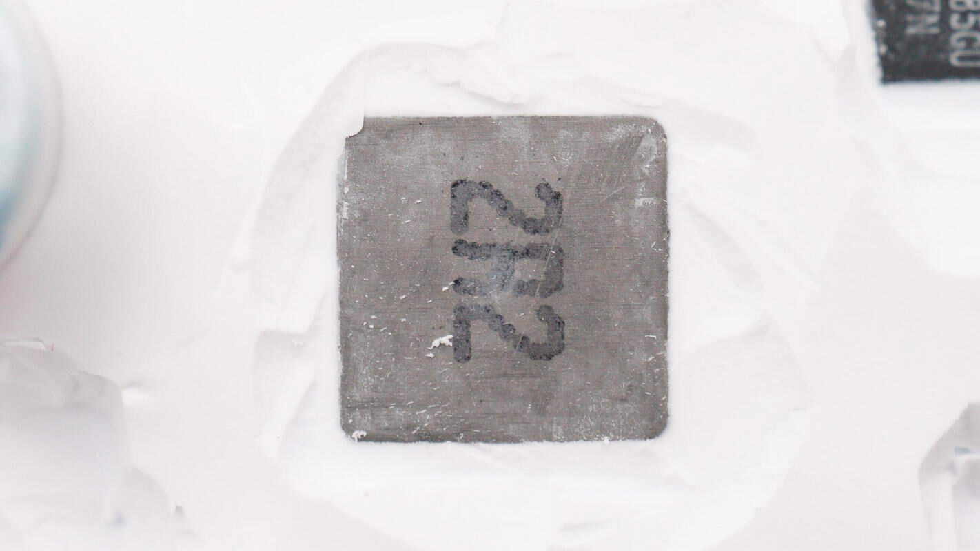
Close-up of the 2.2μH alloy inductor.
Close-up of the VBUS MOSFETs that control the output of the SDC interface.
The VBUS MOSFETs are from NCE, model NCEP035N85GU.
The other VBUS MOSFET is also the same model: NCEP035N85GU.
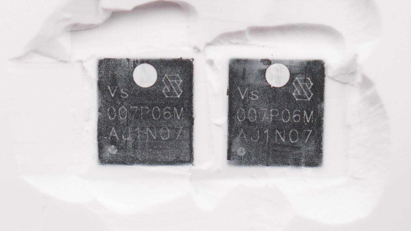
These two VBUS MOSFETs are from Vergiga, model VSP007P06M. They are PMOS transistors with a voltage rating of 60V and an on-resistance of 7.5mΩ, packaged in a PDFN5060X package.
Here is the information about Vergiga VSP007P06MS.
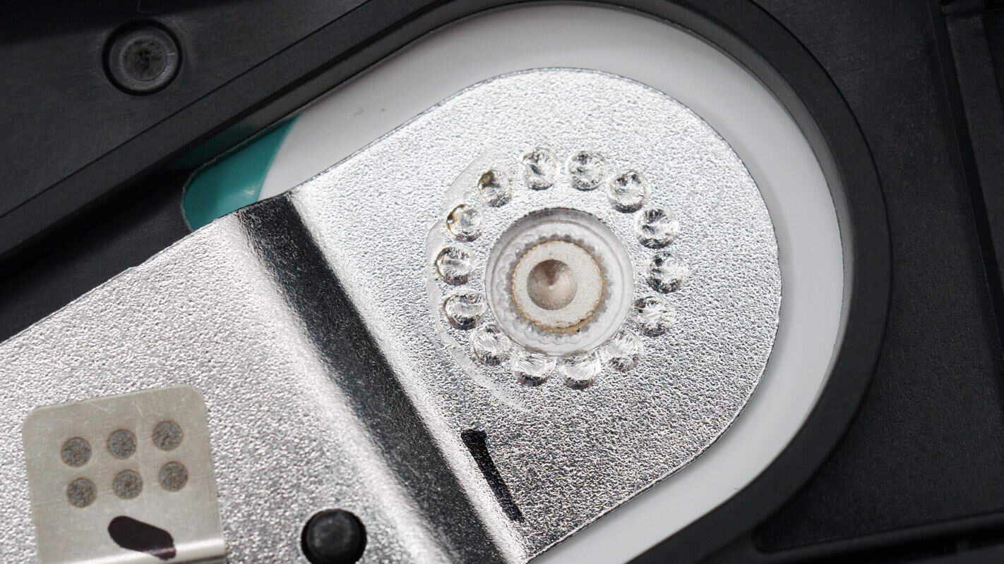
There is a round buzzer located on the protection PCB.
The SDC interface has positive and negative terminals on either side, with communication pins located in the center.
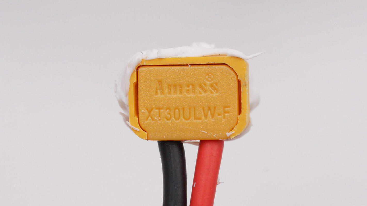
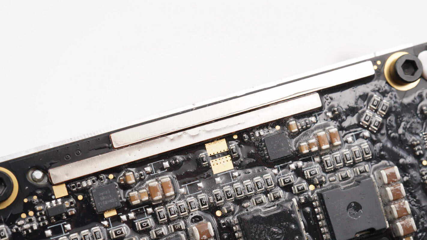
Close-up of the XT30 connector that connects to the panel.
The battery pack is secured with a plastic frame, and a mica sheet is placed at the corresponding position of the protection PCB for insulation.
Foam tape is applied to the bottom of the plastic frame for cushioning.
White adhesive pads are attached to the sides of the plastic frame.

Close-up of the mica sheet used for insulation.
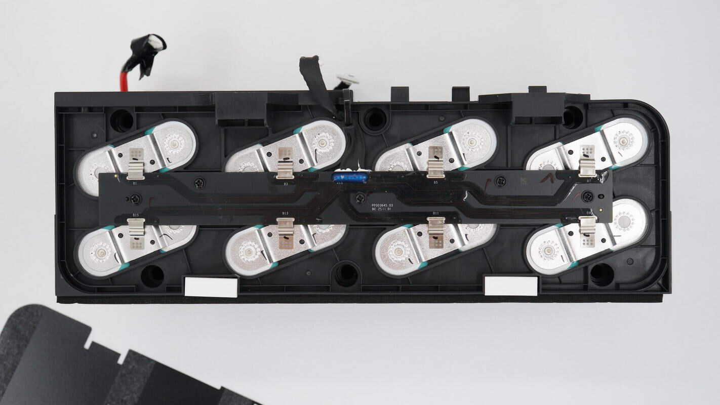
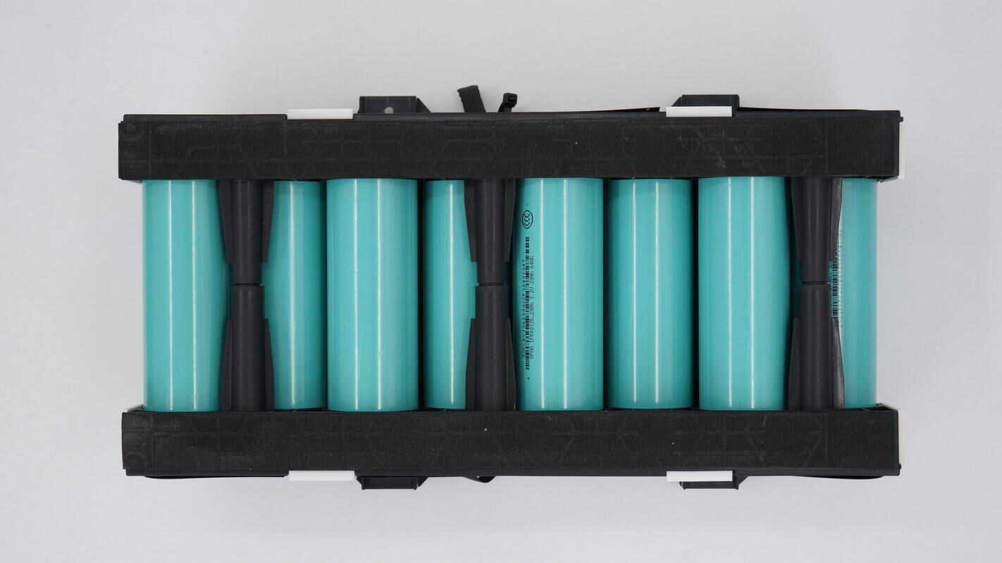
After peeling off the Mylar sheet on the side, you can see that the battery pack’s plastic frame is secured with screws. The battery cells are connected by nickel strips via spot welding, and a small PCB on the side is used for individual cell voltage sampling.
Close-up of the nickel strip spot welding on the battery’s positive terminal.
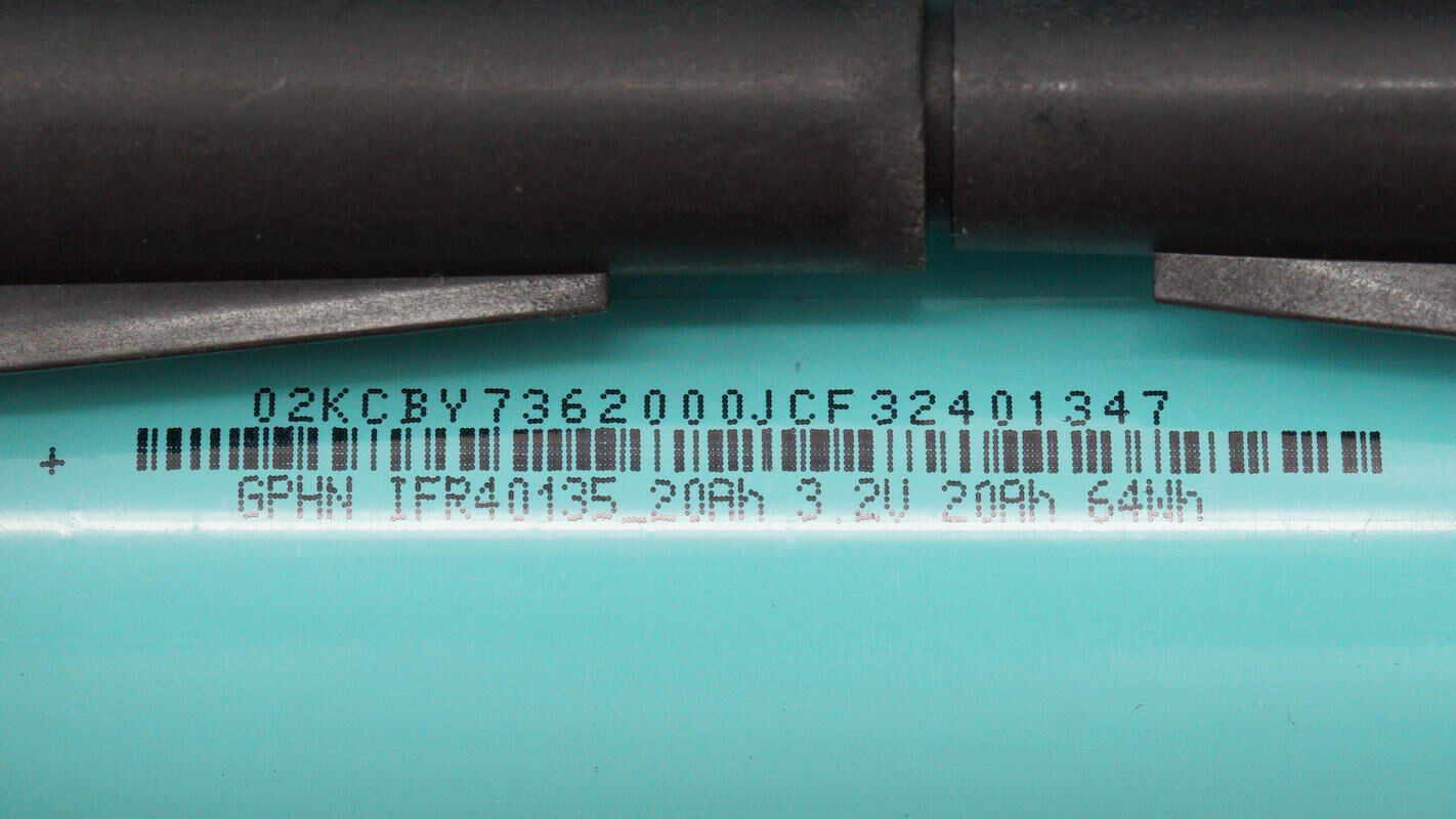
The lithium iron phosphate battery cells are from GPHN, model GPHN IFR40135-20Ah. Each cell has a voltage of 3.2V, a capacity of 20Ah, and an energy rating of 64Wh. The battery pack consists of 16 cells connected in series.
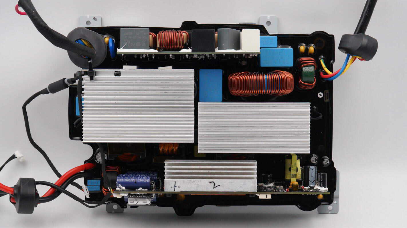
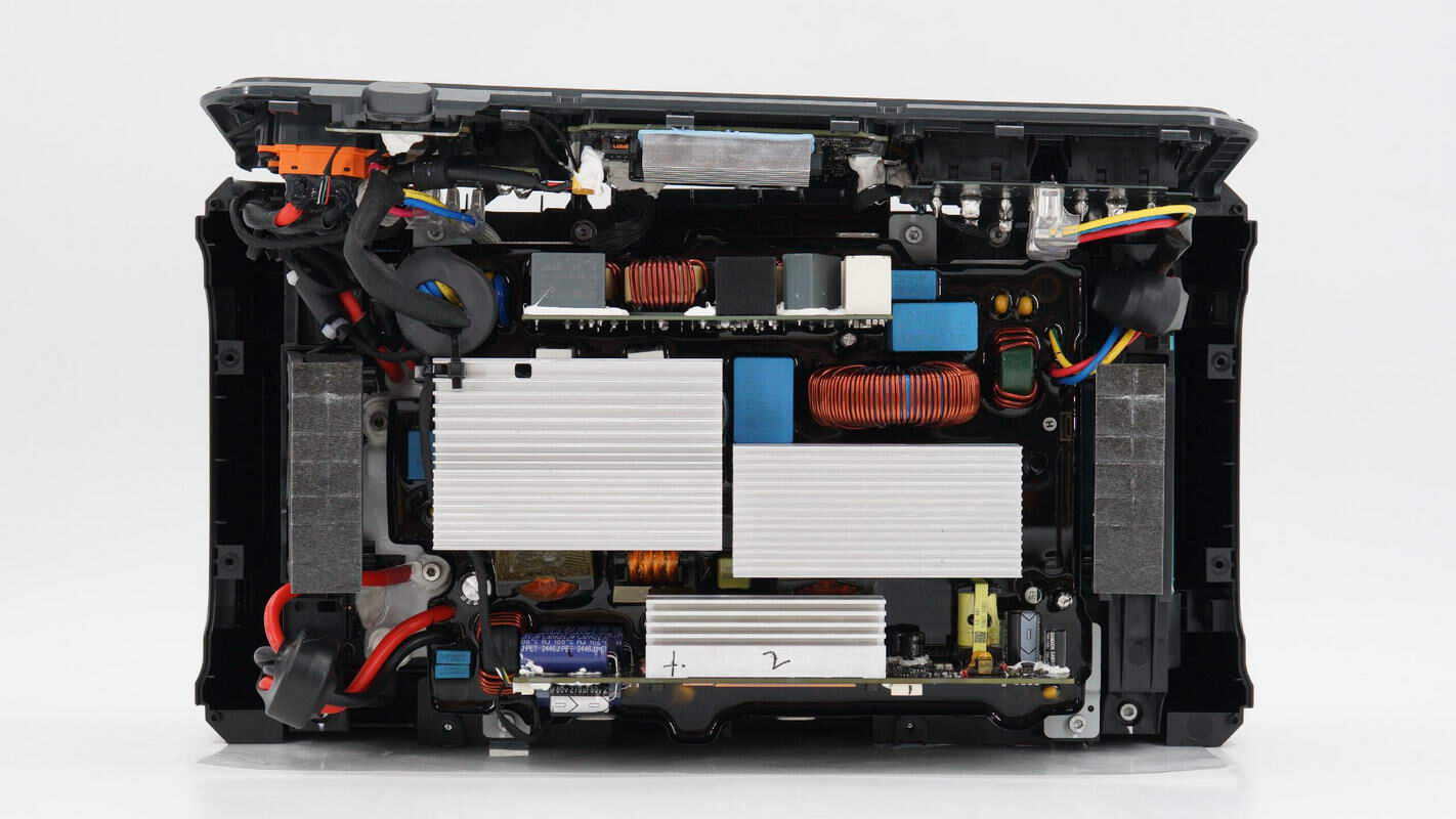
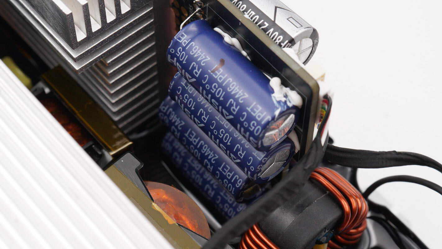
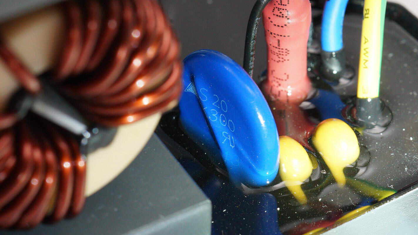
On the front side of the bidirectional inverter module, the upper section features an AC filter PCB. In the middle, there is a heatsink and a PFC inductor. The lower PCB contains the inverter boost and MPPT circuits, with heatsinks positioned over the MOSFETs. The PCBA module is housed in a plastic enclosure filled with hard potting compound internally.
The back of the bidirectional inverter module is secured with a metal plate.
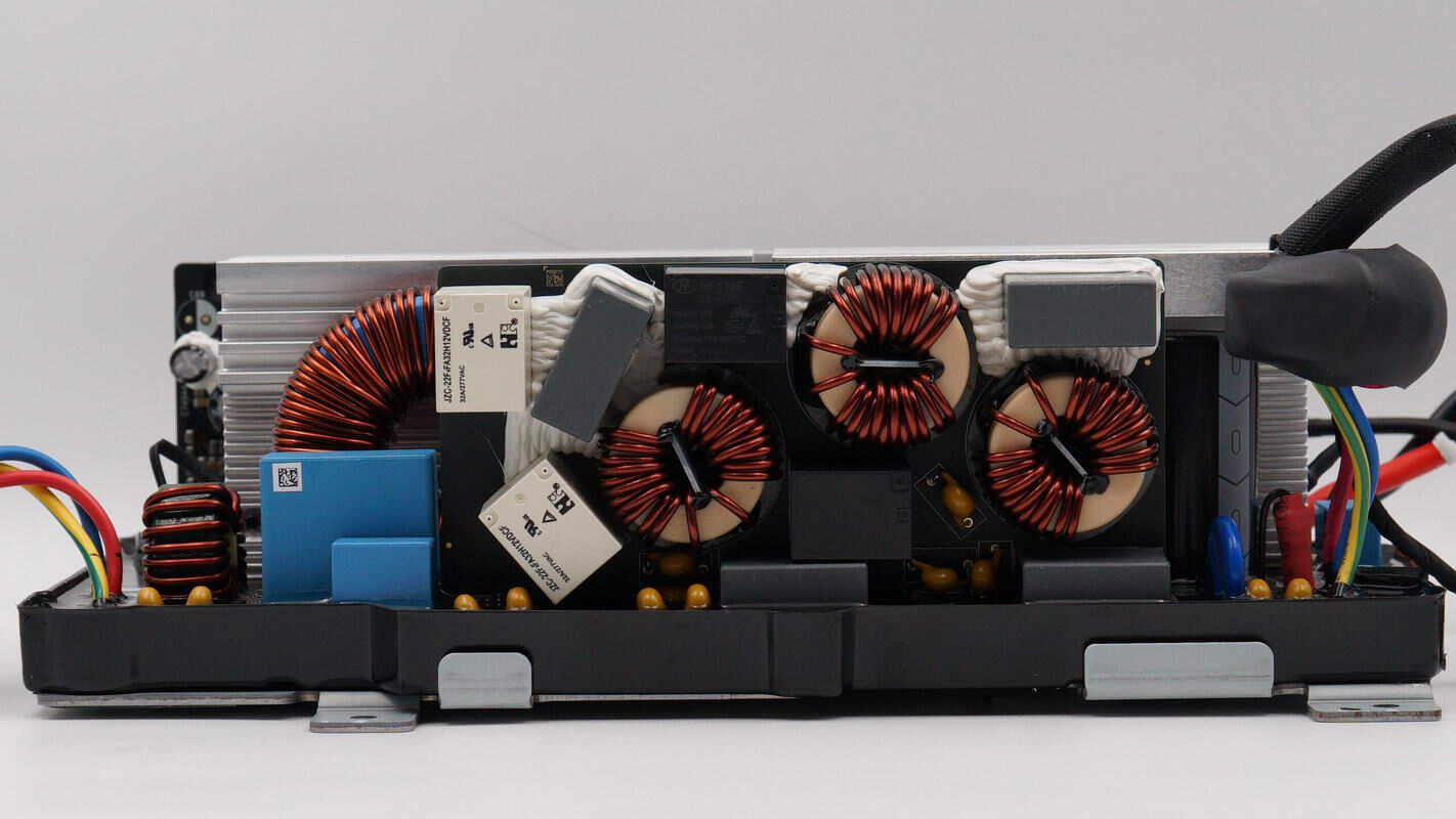
The input-side PCB features safety X2 capacitors, common mode chokes, and relays.
On the side, there are filter capacitors and a boost transformer.
On the other side, the vertical PCB houses the MCU, boost MOSFET, and MPPT MOSFET.
There is an auxiliary power supply on the right side.
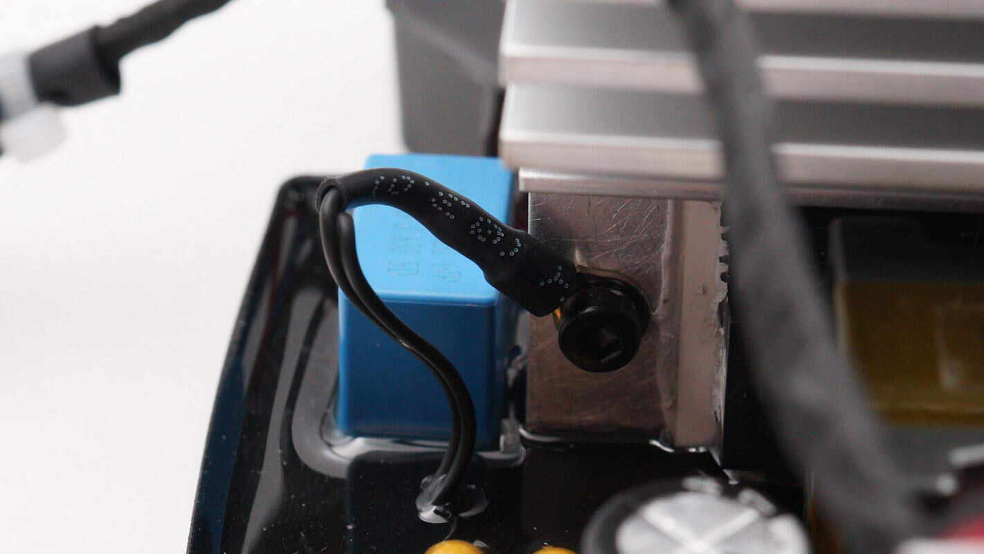
The battery’s positive and negative connection wires are equipped with ferrite beads to suppress high-frequency interference.
The two film capacitors are from TDK.
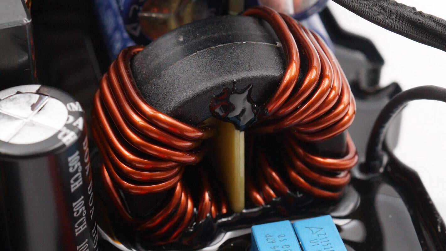
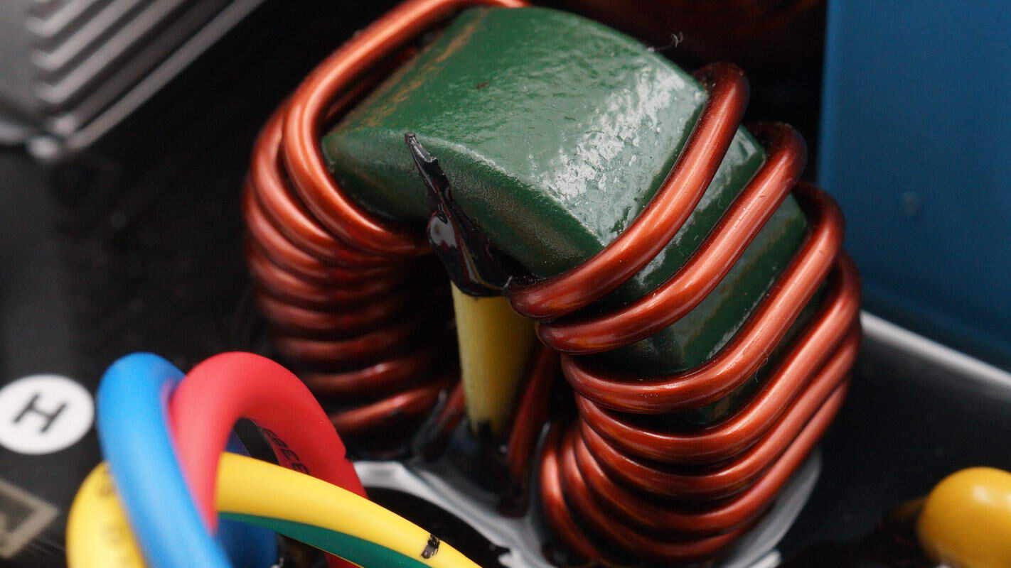
The filter inductor is wounded with magnetic ring.
Close-up of the electrolytic capacitors and sampling resistors.
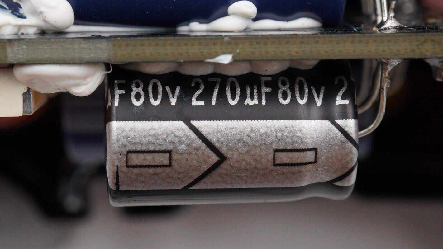
Both filter capacitors are rated at 270μF and 80V.
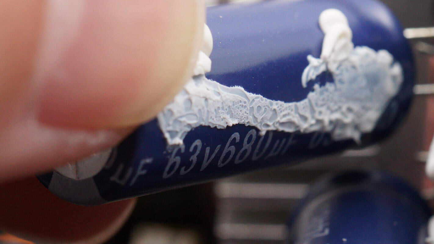
Both filter capacitors are rated at 680μF and 63V.
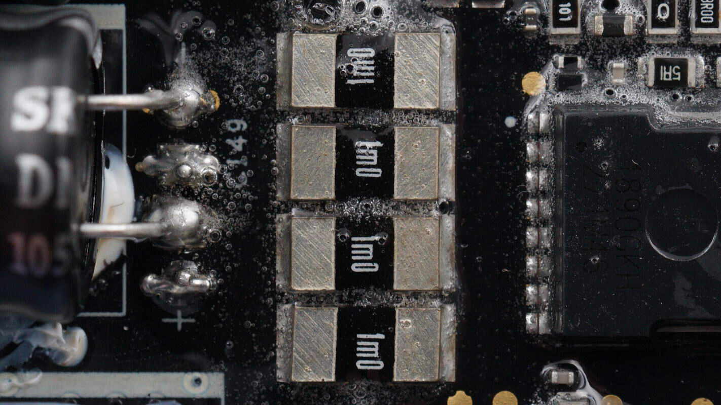
Four 1mΩ resistors are connected in parallel for current sensing.
Four filter capacitors are soldered on the back of the small PCB and secured with potting compound.
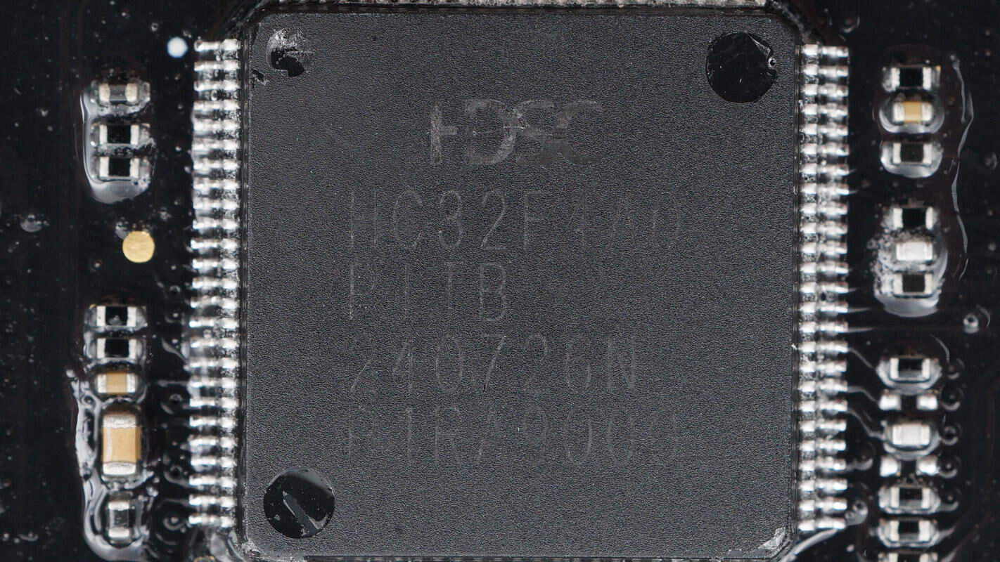
The MCU of the bidirectional inverter module is from XHSC, model HC32F4A0PITB-LQFP100. It features a Cortex-M4 CPU with integrated FPU, MPU, and DSP, running at a maximum clock speed of 240MHz. It also integrates 2MB of FLASH memory and 512+4KB of SRAM, packaged in an LQFP100 form factor.
The PCB is reinforced with copper bars to enhance current-carrying capacity.
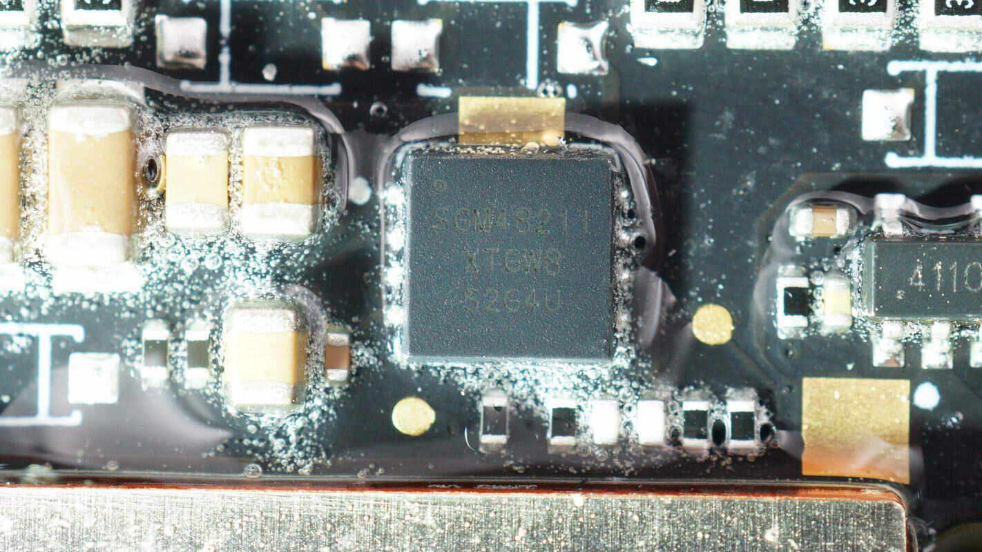
The two drivers are from SGMICRO, model SGM48211. They are half-bridge drivers with a voltage rating of 120V, featuring fully independent high-side and low-side channels. The chips support a peak current of 4A and integrate bootstrap diodes, packaged in TDFN 4×4 mm form factors.
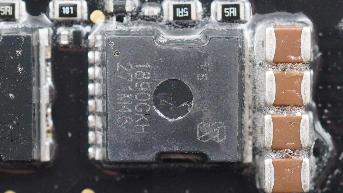
The eight MOSFETs are from Vergiga, model VS1890GKH. They are NMOS transistors with a voltage rating of 100V and an on-resistance of 1.3mΩ, packaged in TOLL packages. Four MOSFETs form a group for inverter boost, and the other four form a group for MPPT.
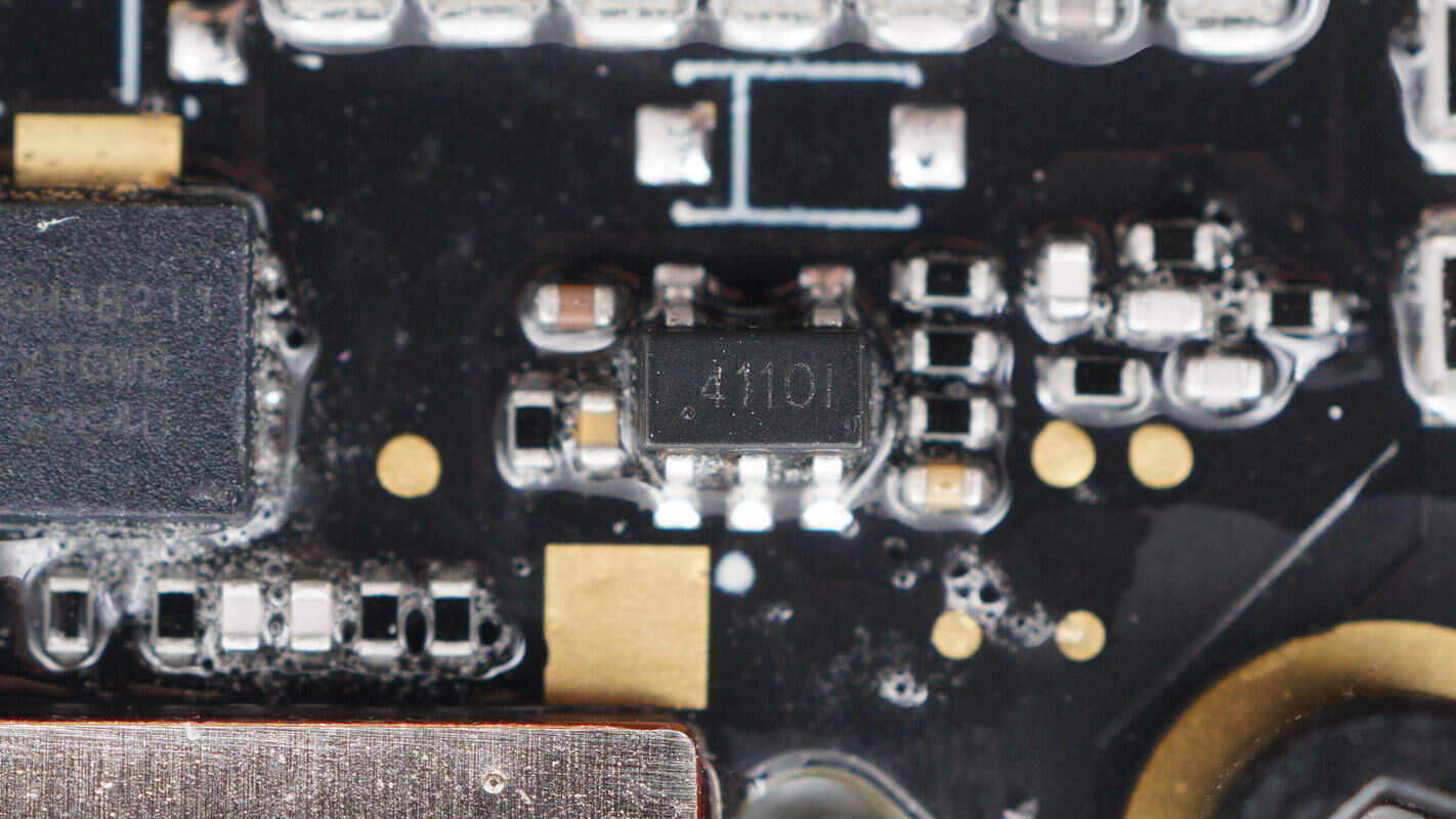
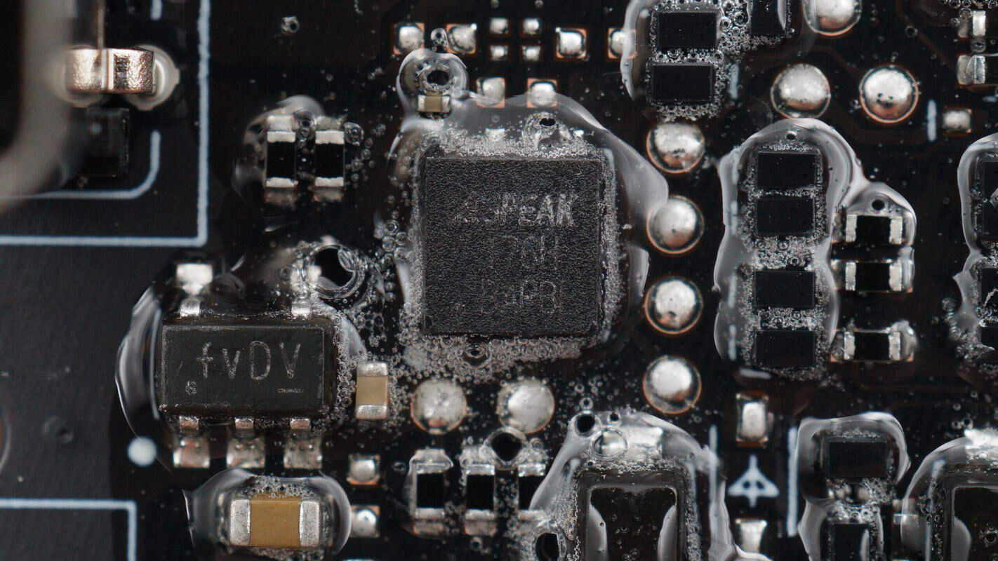
The single operational amplifier is from 3PEAK, marked with 411, model TP2411. It is a low-noise rail-to-rail op-amp with an output current of 70mA, packaged in a SOT23-5 form factor.
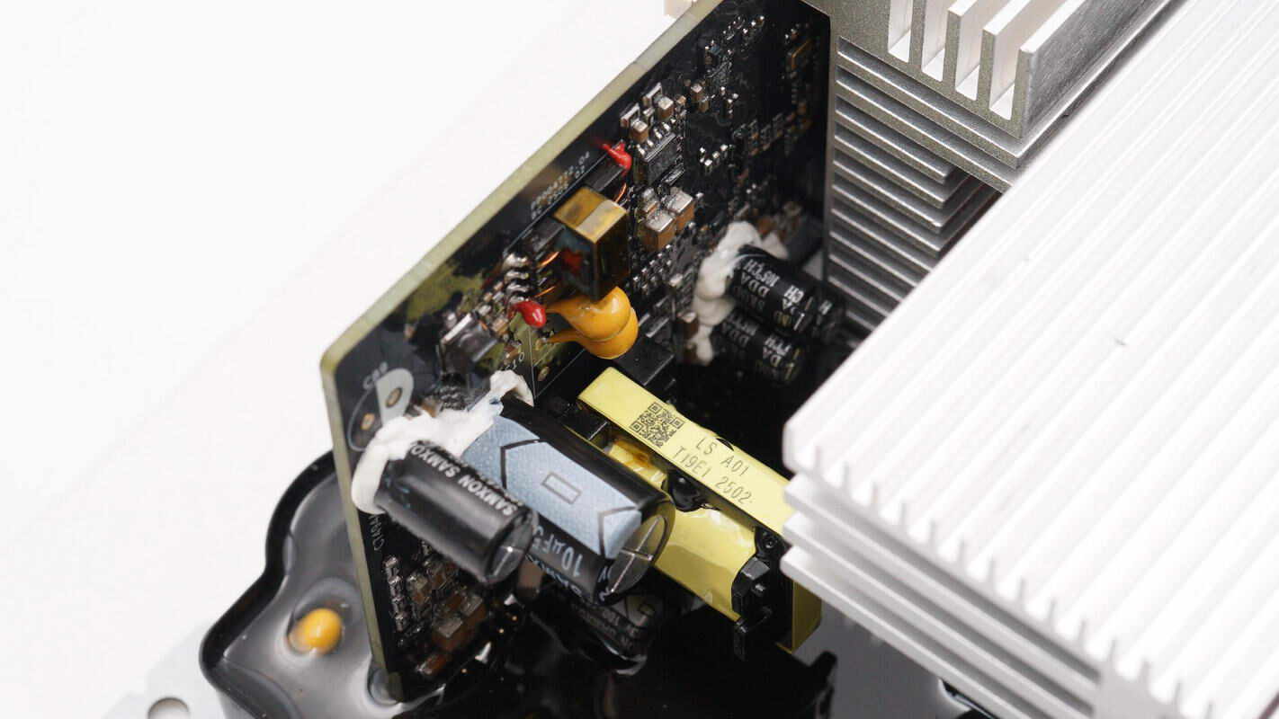
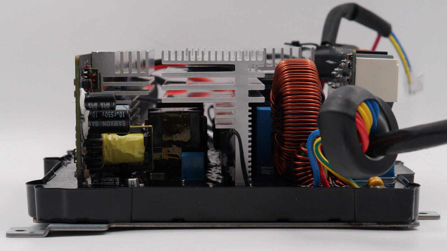
The auxiliary power supply is located on the other side.
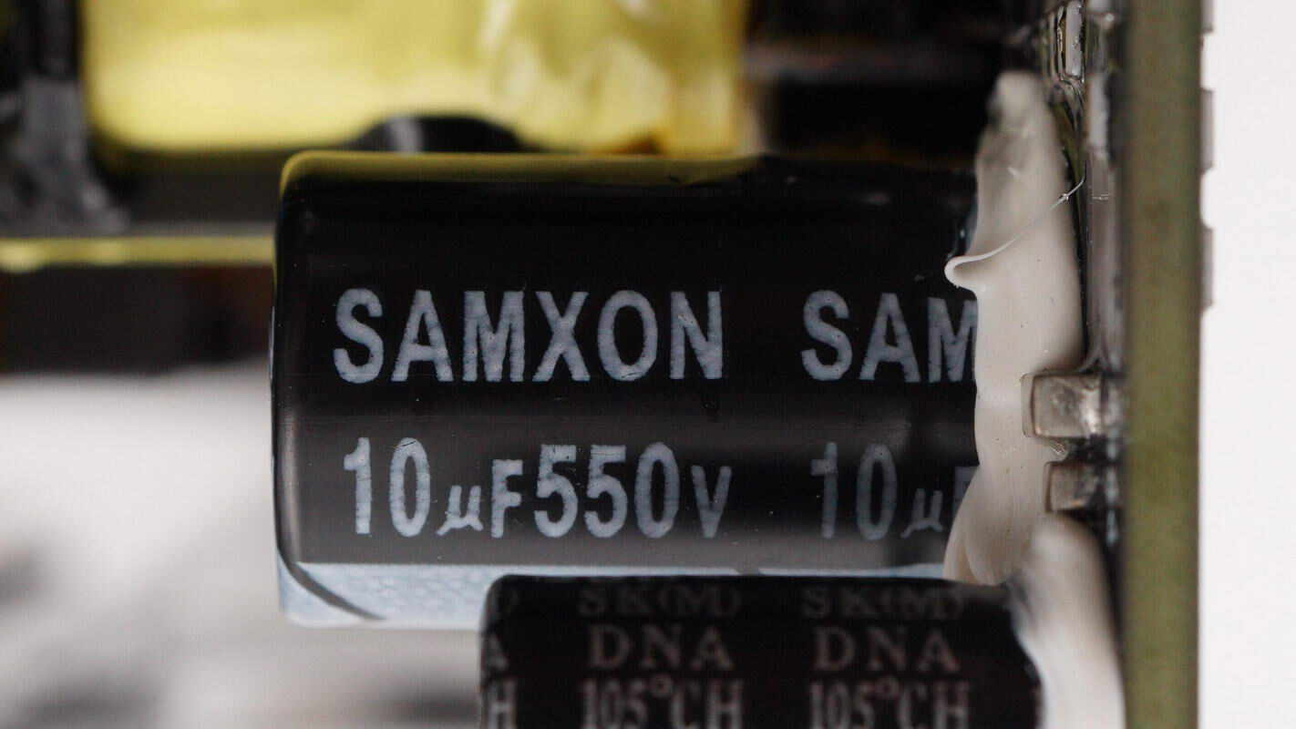
The high-voltage filter capacitor is from SAMXON. 10μF 550V.
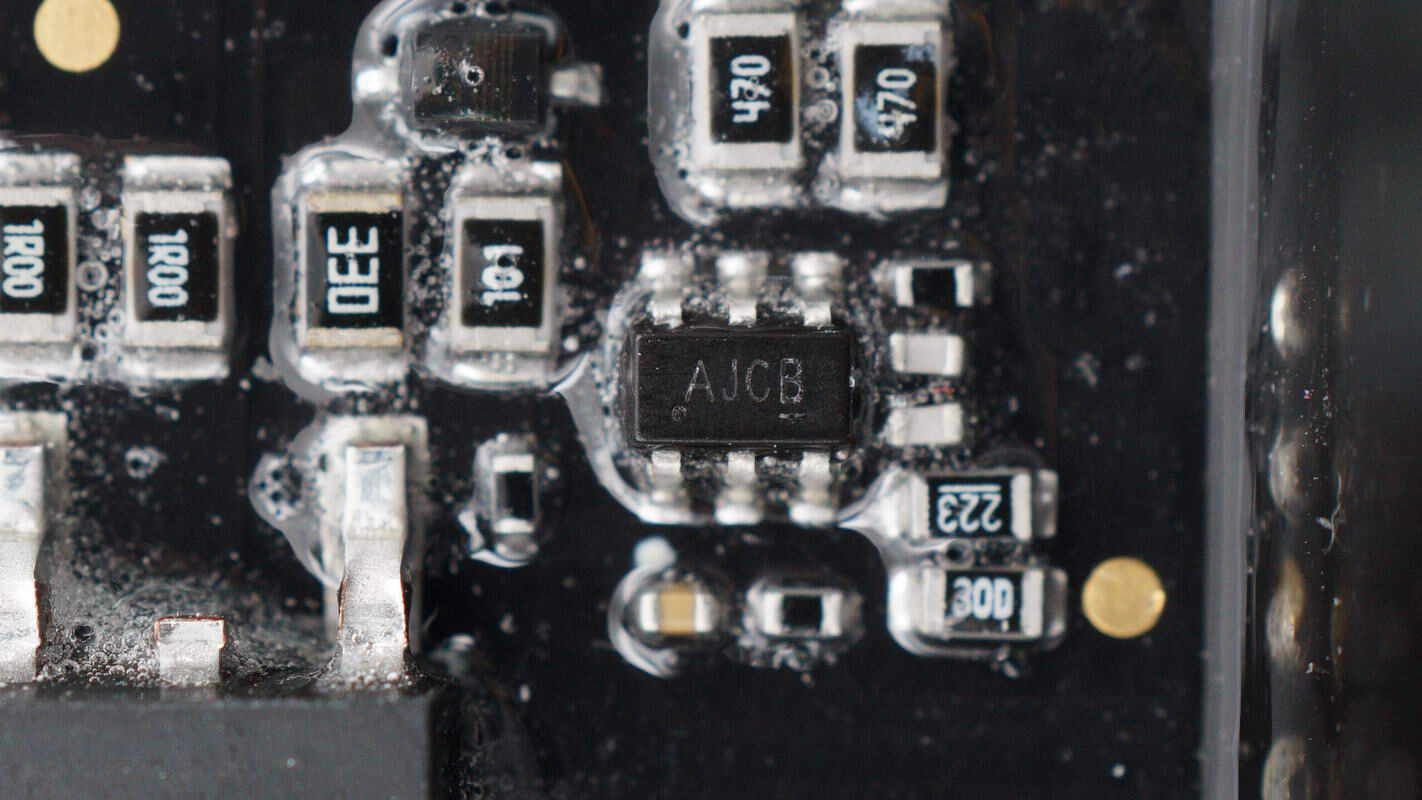
The primary master control chip is from ETA, marked with AJ, model ETA8076. It is a high-frequency quasi-resonant flyback controller supporting a supply voltage range of 7–77V, with a maximum switching frequency of 140kHz. It features adaptive loop compensation, standby power consumption below 75mW, meets Level VI energy efficiency standards, and is packaged in a SOT23-6 form factor.

Here is the information about ETA ETA8076.
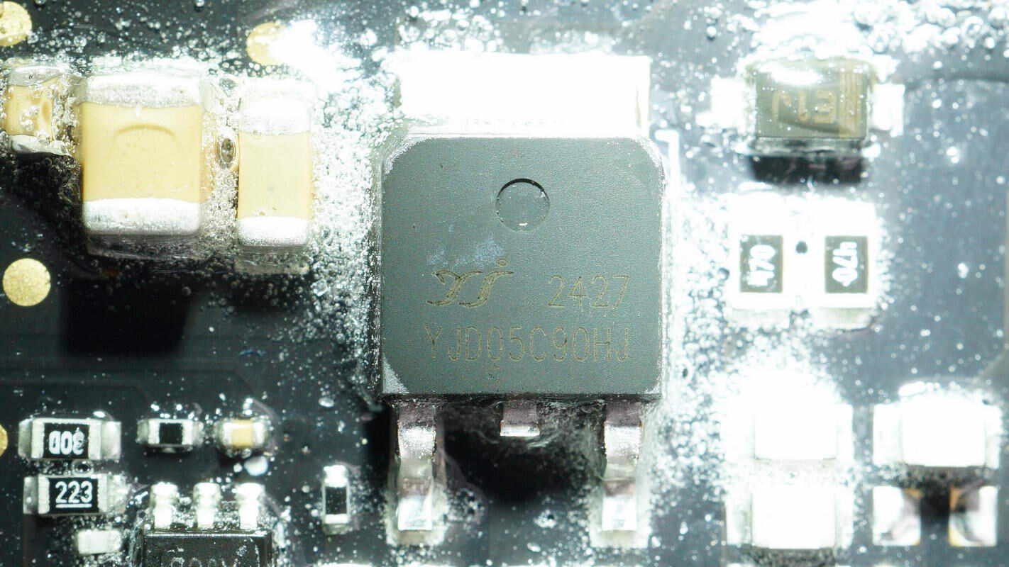
The primary MOSFET is from YJ, model YJD05C90HJ. It is an NMOS with a voltage rating of 900V and an on-resistance of 1.1Ω, packaged in a TO-252 form factor.
The auxiliary power transformer’s magnetic core is reinforced with potting glue.
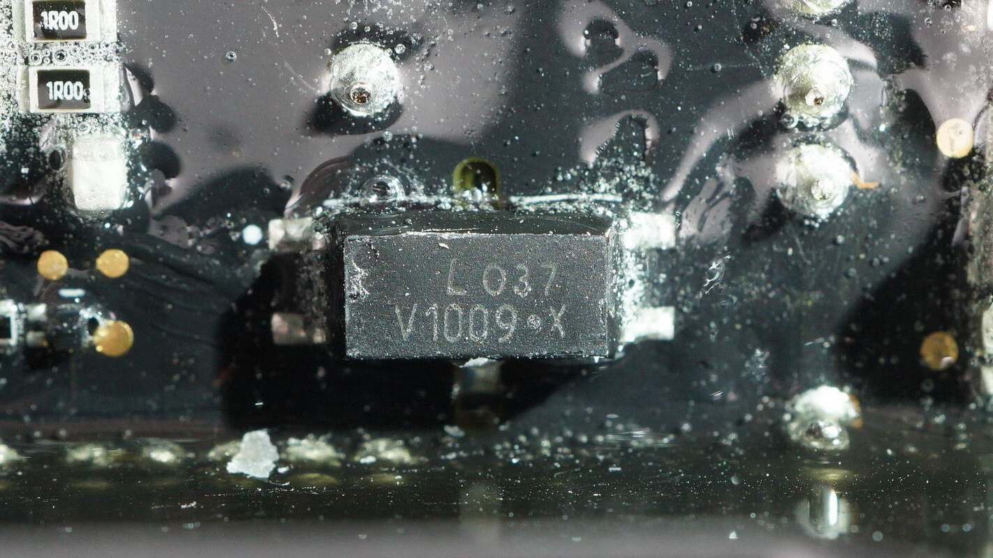
The LITEON LTV-1009 optocoupler is used for output voltage feedback.
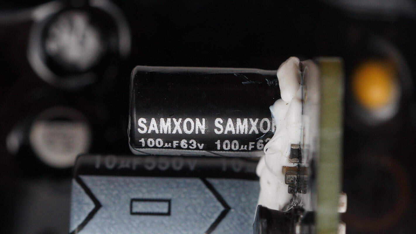
The filter capacitor is from SAMXON. 100μF 63V.
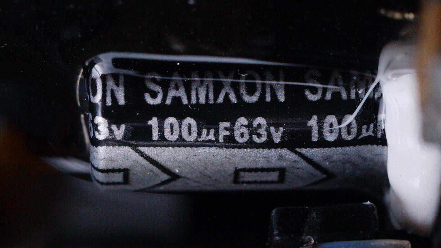
The other filter capacitor has the same specifications.
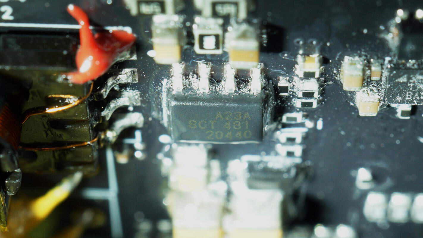
The buck chip is from Silicon, model SCT2A23A. It is a 100V-rated step-down converter with a 1.2A output current. The chip integrates internal MOSFETs, operates at a fixed switching frequency of 300kHz, and comes in an ESOP8 package.
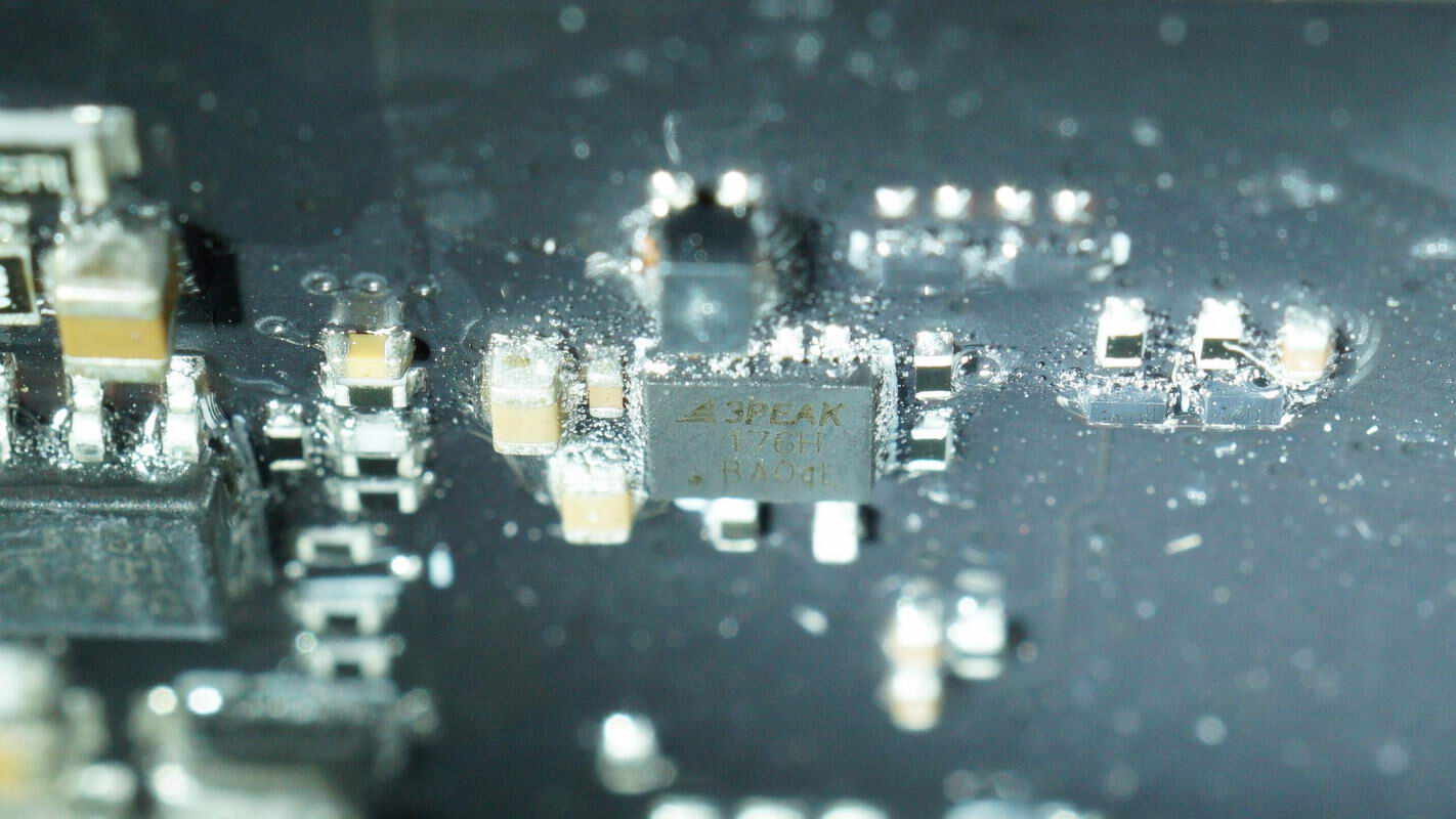
The RS485 transceiver is from 3PEAK, model TPT75176H. It features 15kV ESD protection, supports data rates up to 10Mbps, and offers full fault protection. The device is packaged in a DFN 3×3 mm, 8-pin form factor.
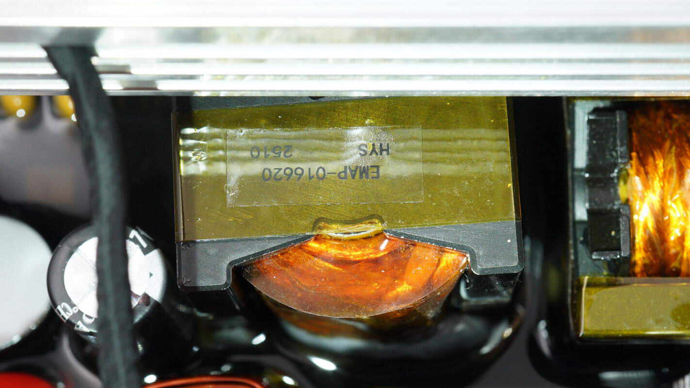
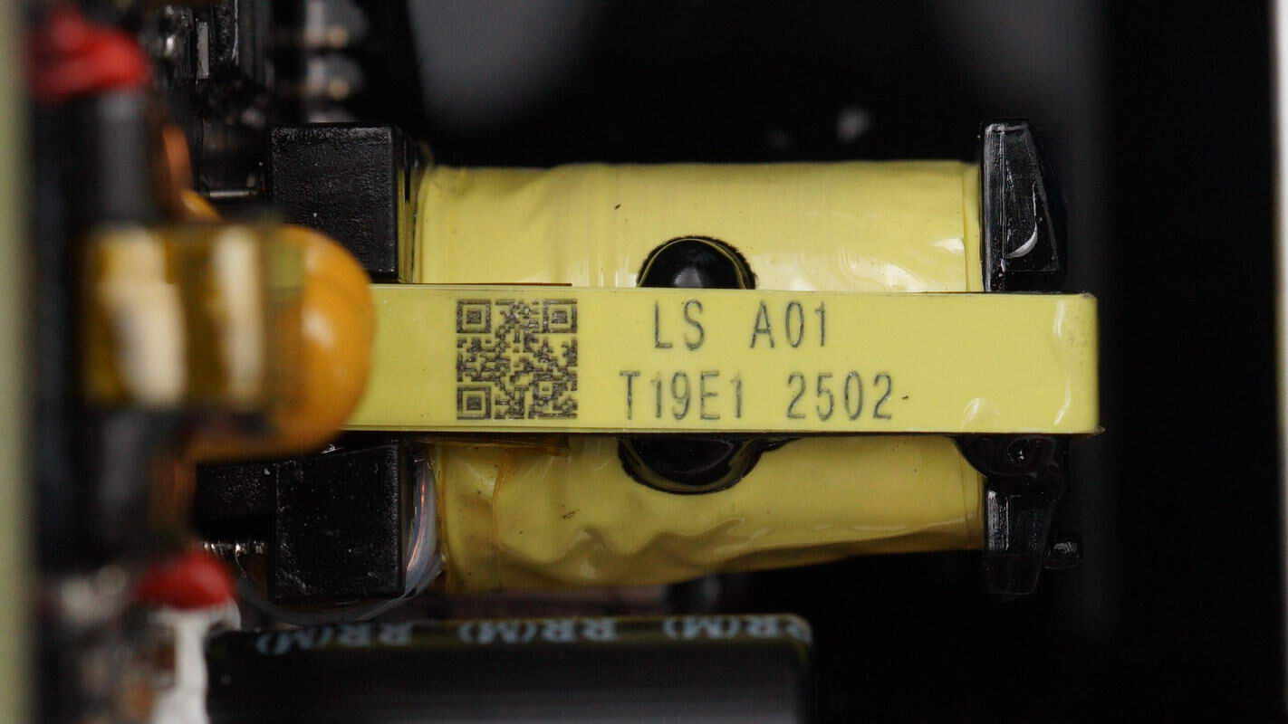
Close-up of the transformer.
Close-up of the resonant inductor.
Close-up of the current transformer.
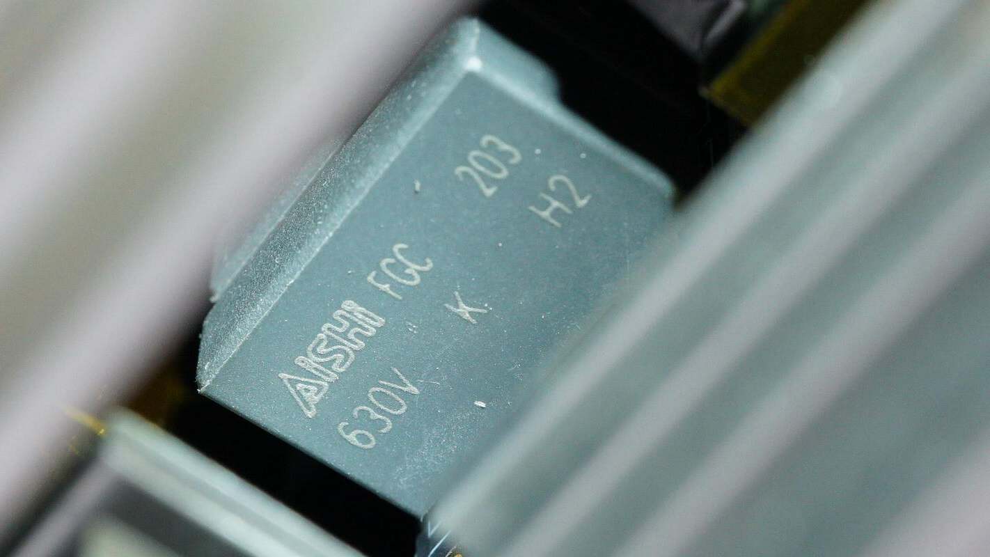
The resonant capacitor is from AiSHi. 0.02μF 630V.
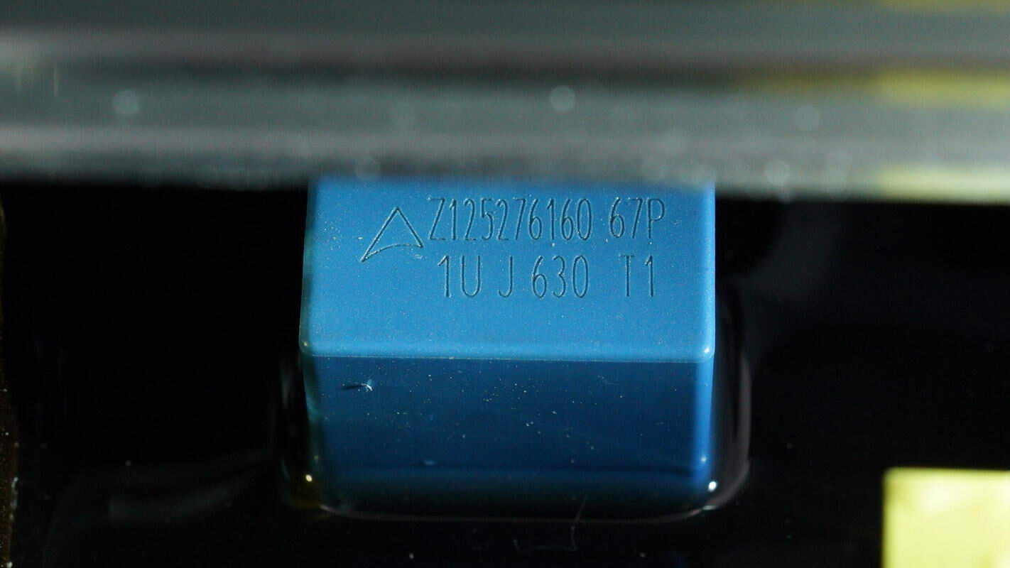
The film filter capacitor is from TDK. 1μF 630V.
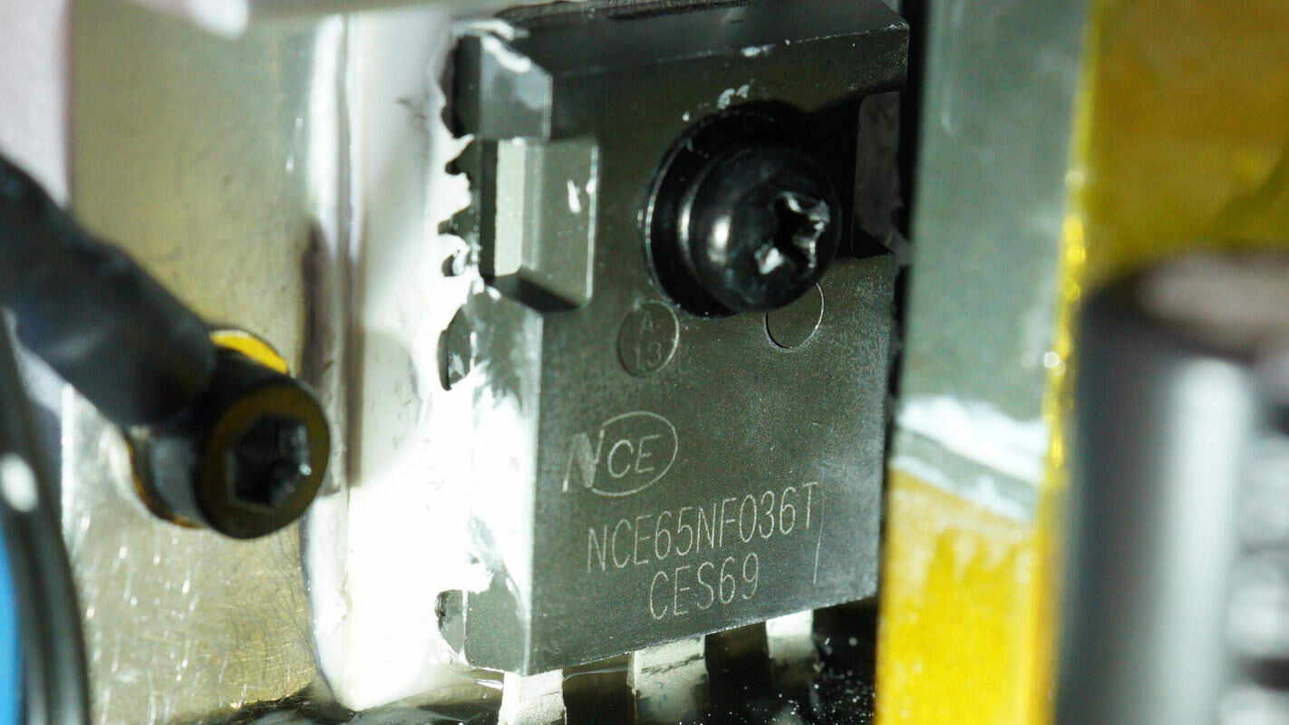
The high-voltage MOSFETs used for the inverter and output modulation are from NCE, model NCE65NF036T. They are NMOS transistors with a voltage rating of 650V and an on-resistance of 30mΩ, packaged in the TO-247 form factor. There are a total of 6 units.
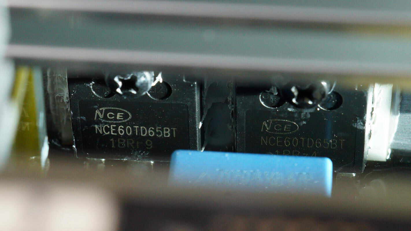
The IGBT is from NCE, model NCE60TD65BT, rated at 650V and 60A, packaged in a TO-247 form factor.
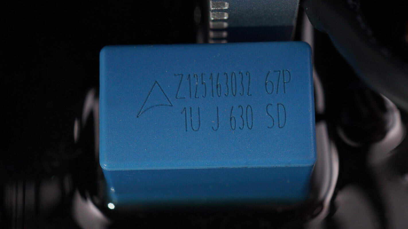
The film filter capacitor has a specification of 1μF, 630V.
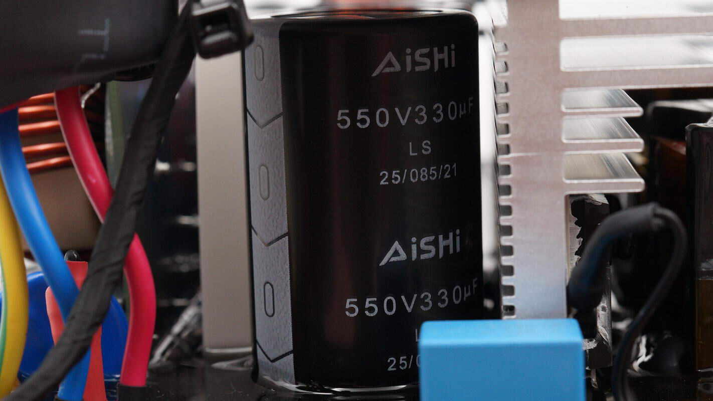
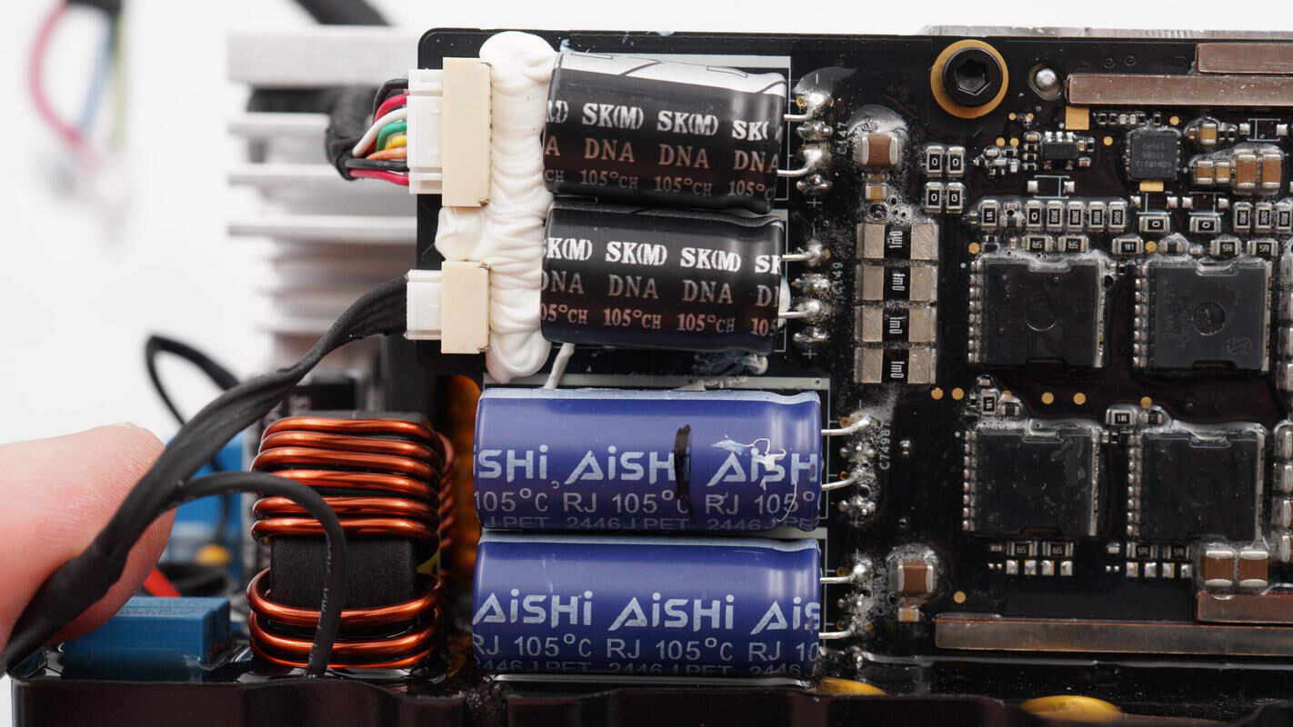
The high-voltage filter capacitors are from AiSHi, each rated at 550V and 330μF, with a total of two units.
Below the heatsink, there are two cement resistors.
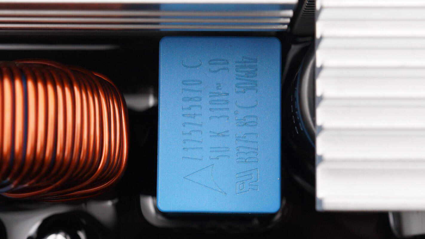
The safety X2 capacitor is from TDK. 5μF.
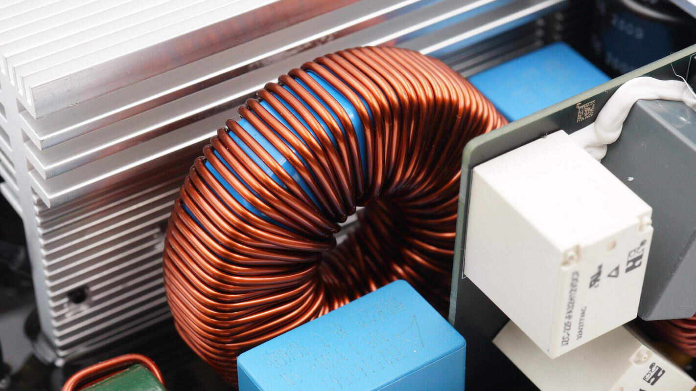
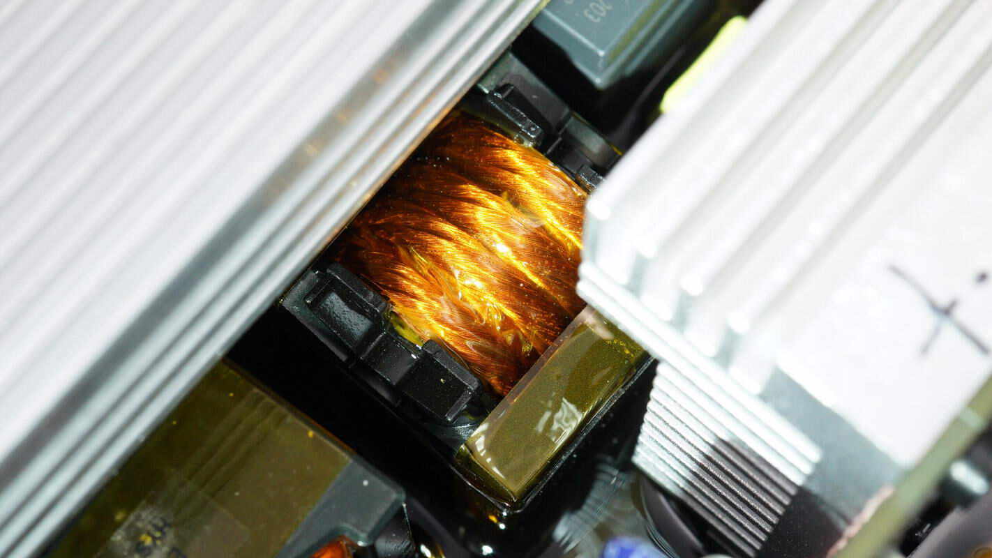
Close-up of the PFC boost inductor.
The safety X2 capacitor has a specification of 3.5μF.
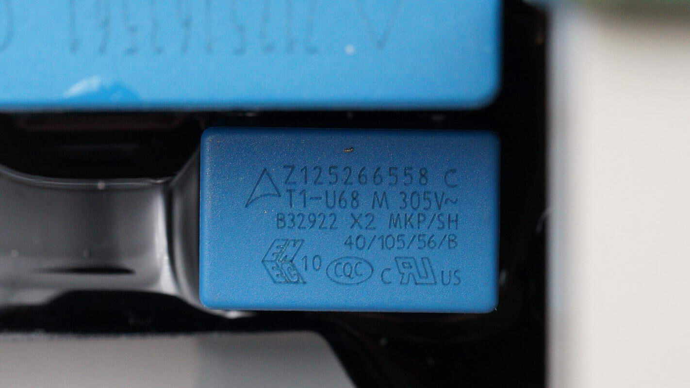
The other safety capacitor has a specification of 0.68μF.
Close-up of the output filter inductor.
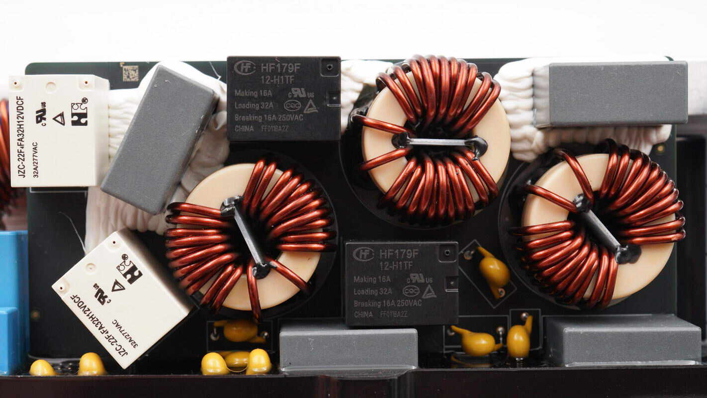
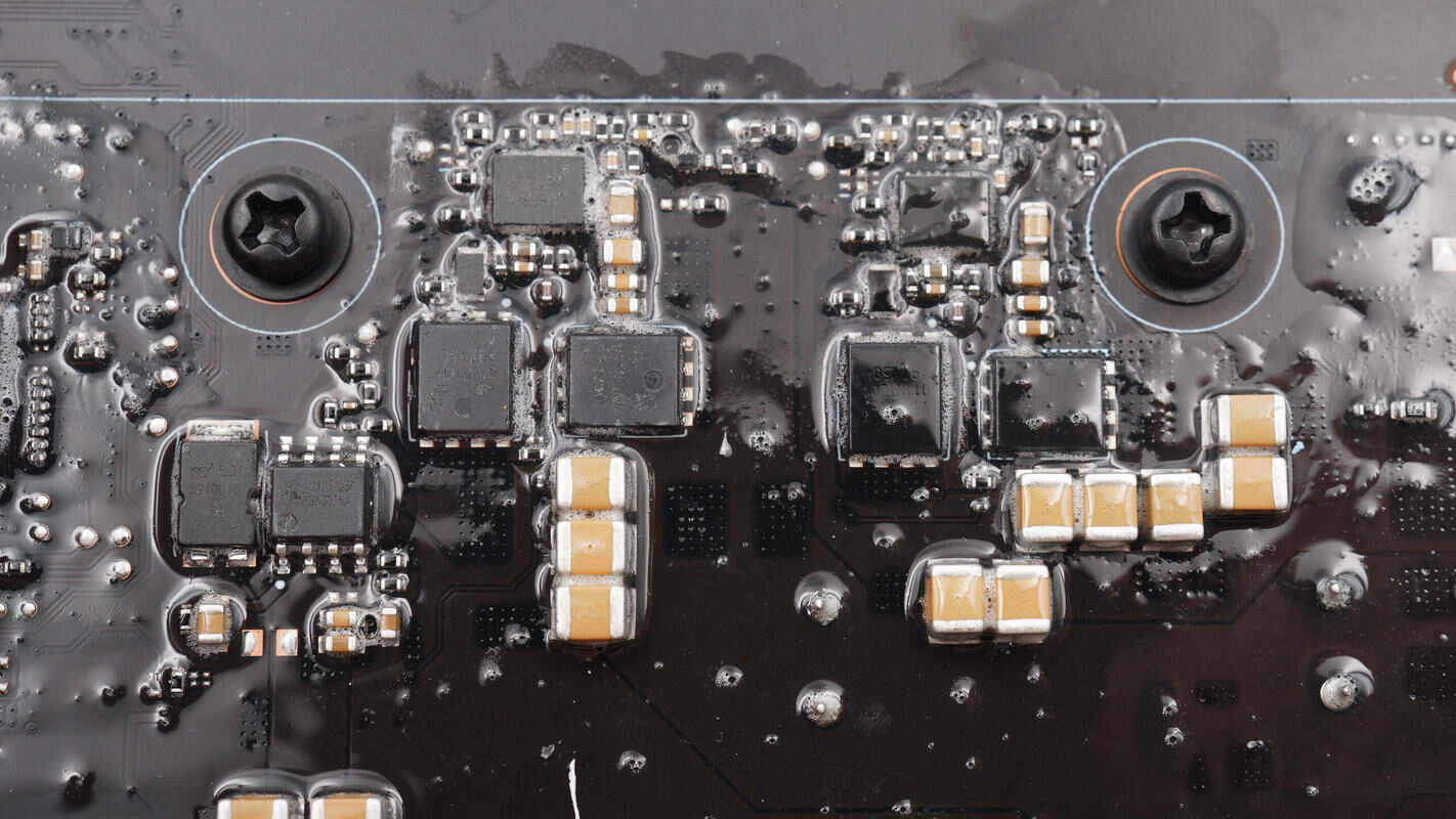
The AC-side PCB of the bidirectional inverter module is equipped with four relays, four safety X2 capacitors, and three common mode chokes. The components are reinforced with potting glue for added durability.
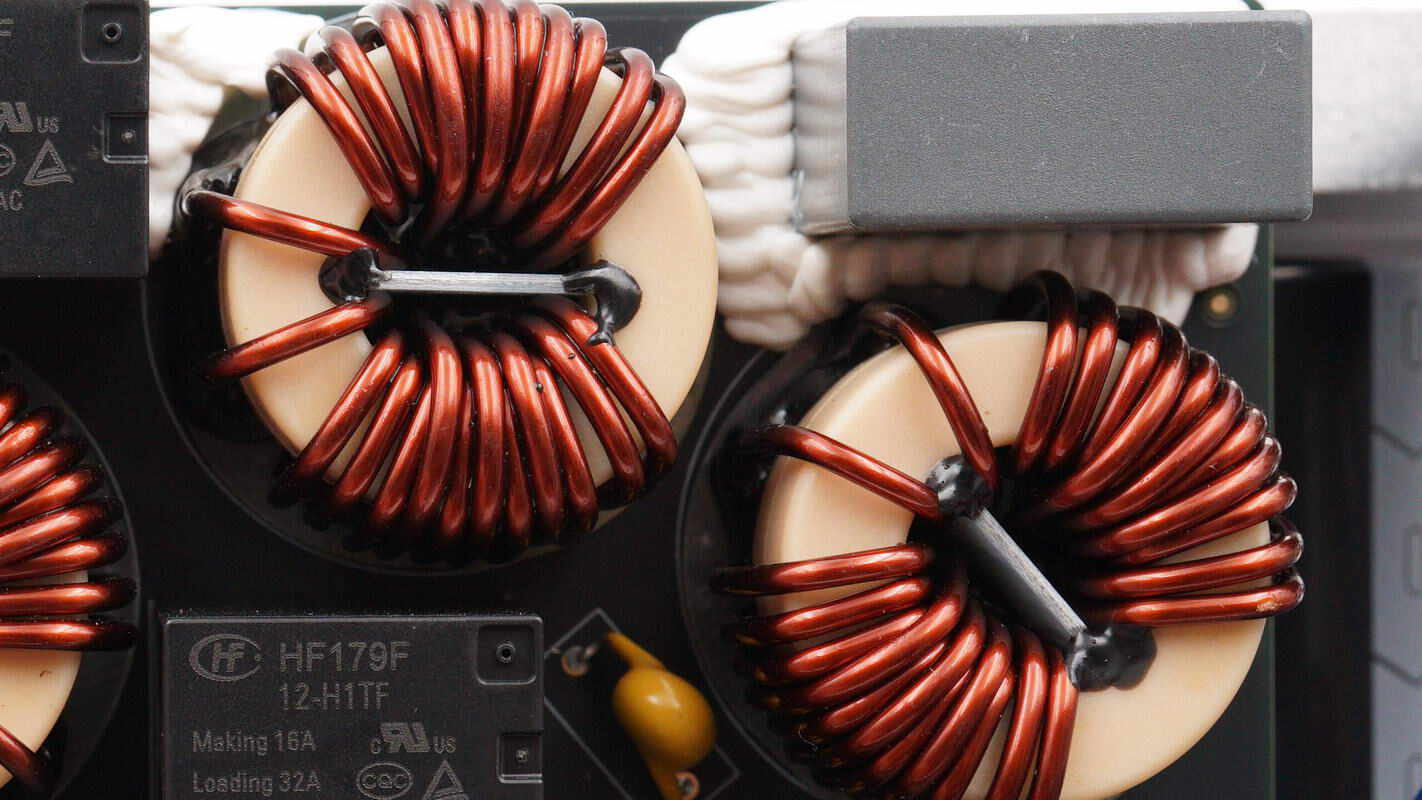
The common mode chokes are wound with magnetic cores and insulated wires, and feature internal insulating plates.
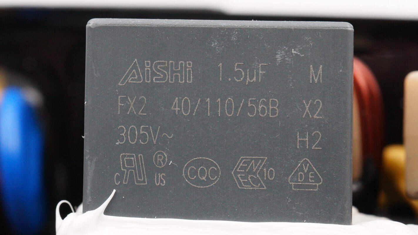
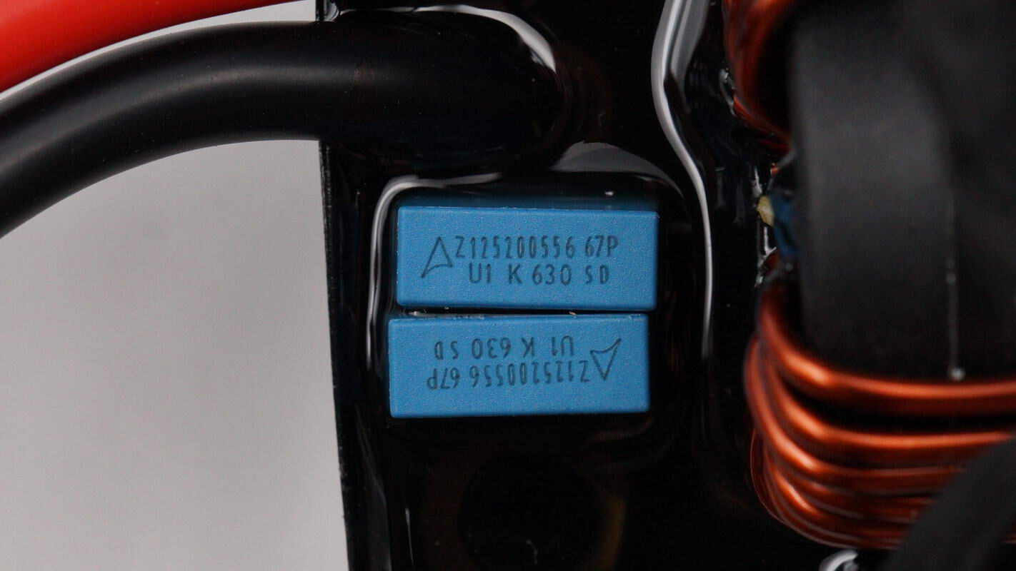
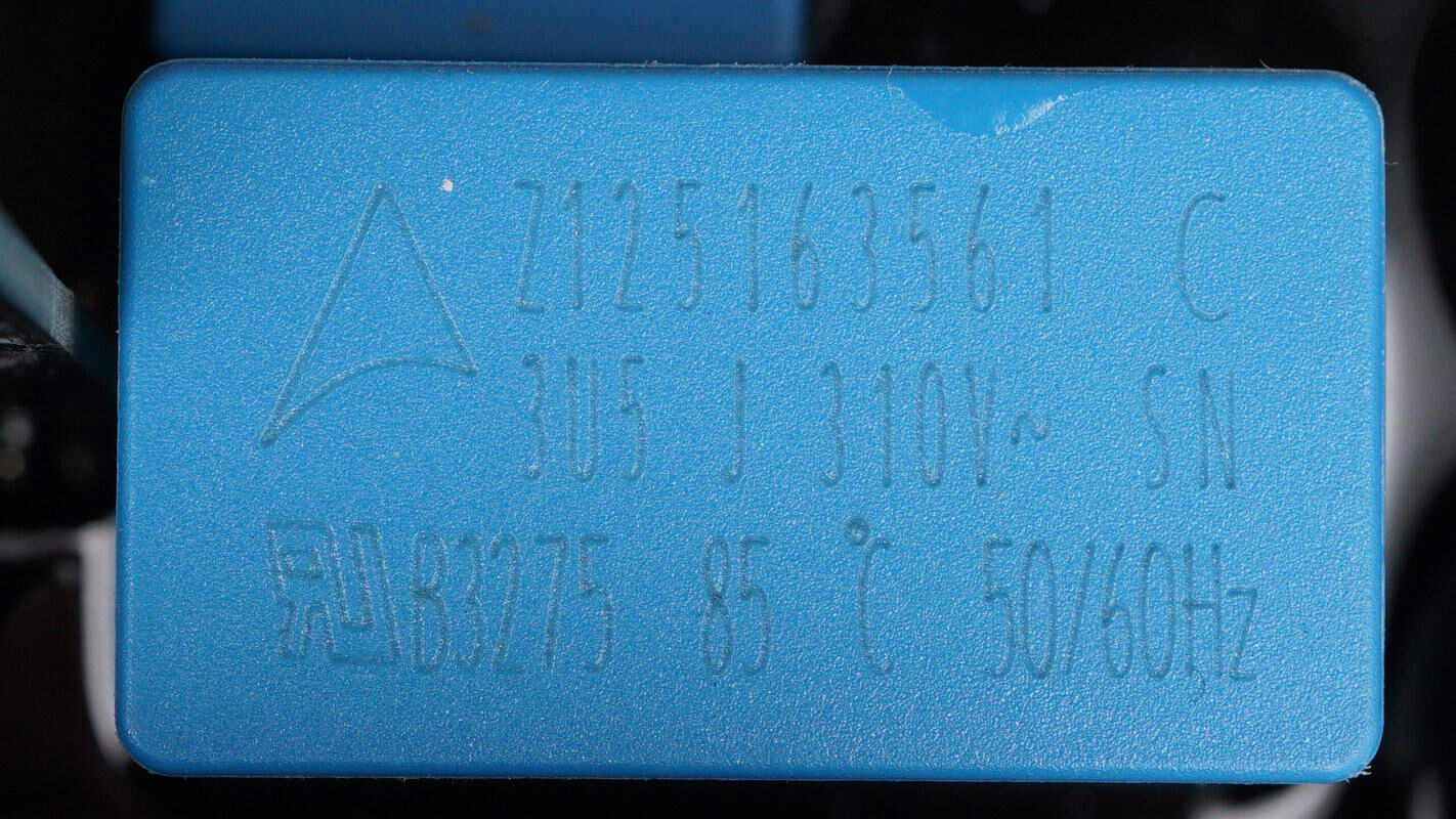
The safety X2 capacitors are from AiSHi. 1.5μF.
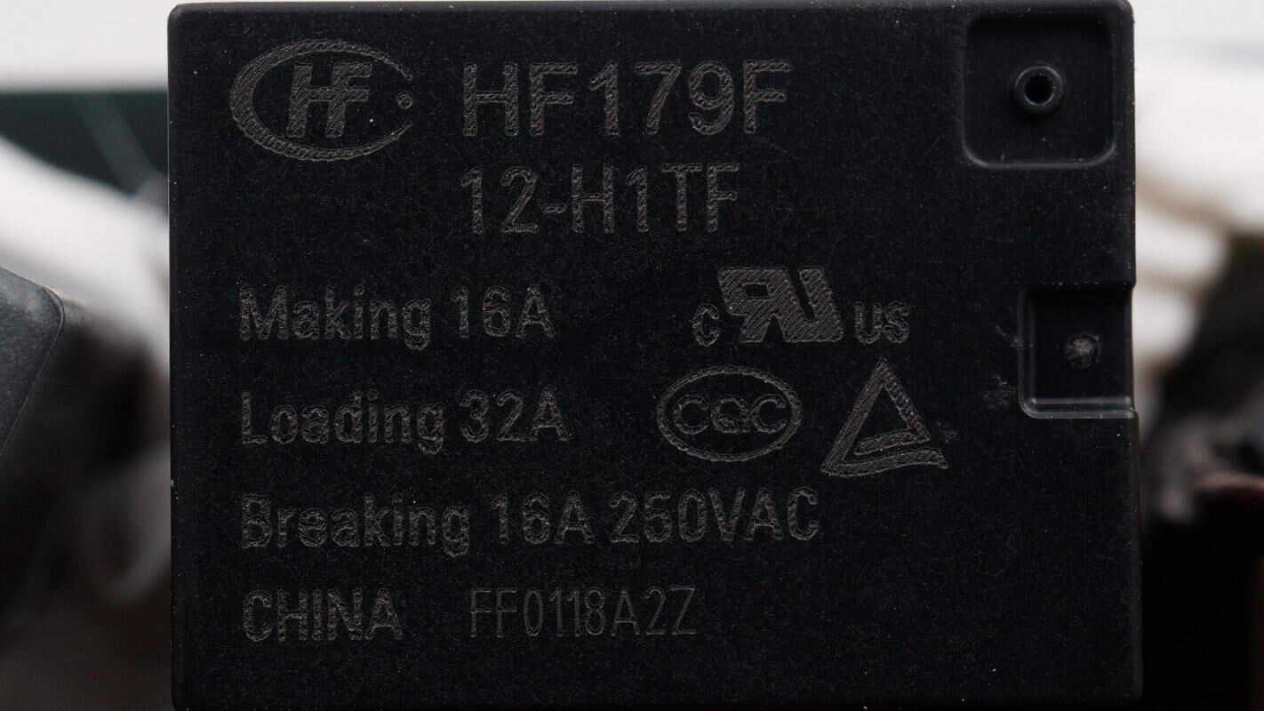
The two black relays are from HONGFA, model HF179F/12-H1TF. Each relay has one set of normally open contacts, with a contact switching capacity of 32A and a coil voltage of 12V.
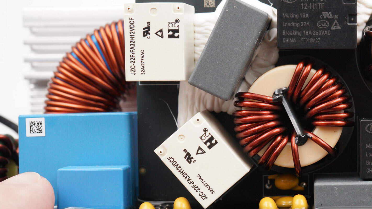
The two white relays are from Forward Relay, model JZC22-F4FA32H12VDCF. Each contains one set of normally open contacts, with a contact load capacity of 32A and a coil voltage of 12V.
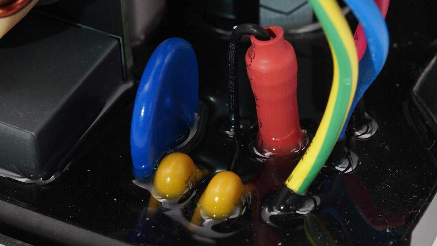
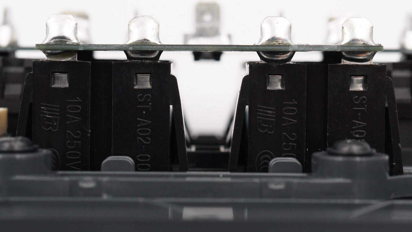
The AC input terminal is equipped with a fuse and a varistor.
The varistor is from TDK.
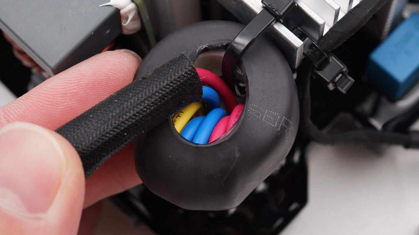
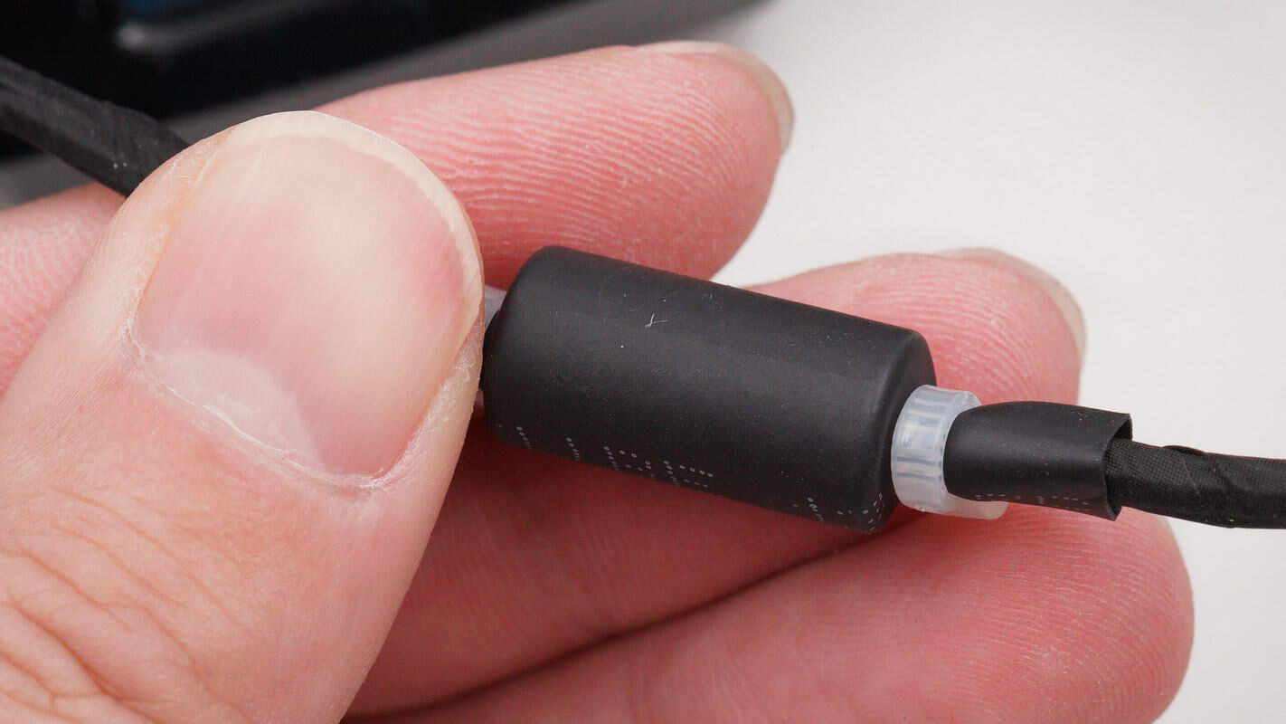
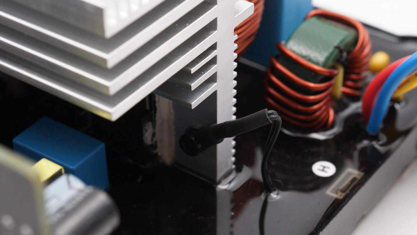
The AC input cable is sleeved with a ferrite core to suppress high-frequency interference and is secured to the heatsink with a cable tie.
The signal wires are sleeved with ferrite cores to suppress high-frequency interference.
A thermistor is installed on the heatsink to monitor temperature.
The other heatsink also has a thermistor installed.
The AC output sockets are connected via soldered joints on the PCB.
The solder joints are well wetted and fully covered with solder.
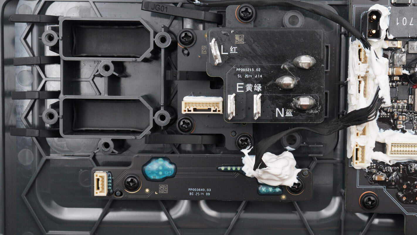
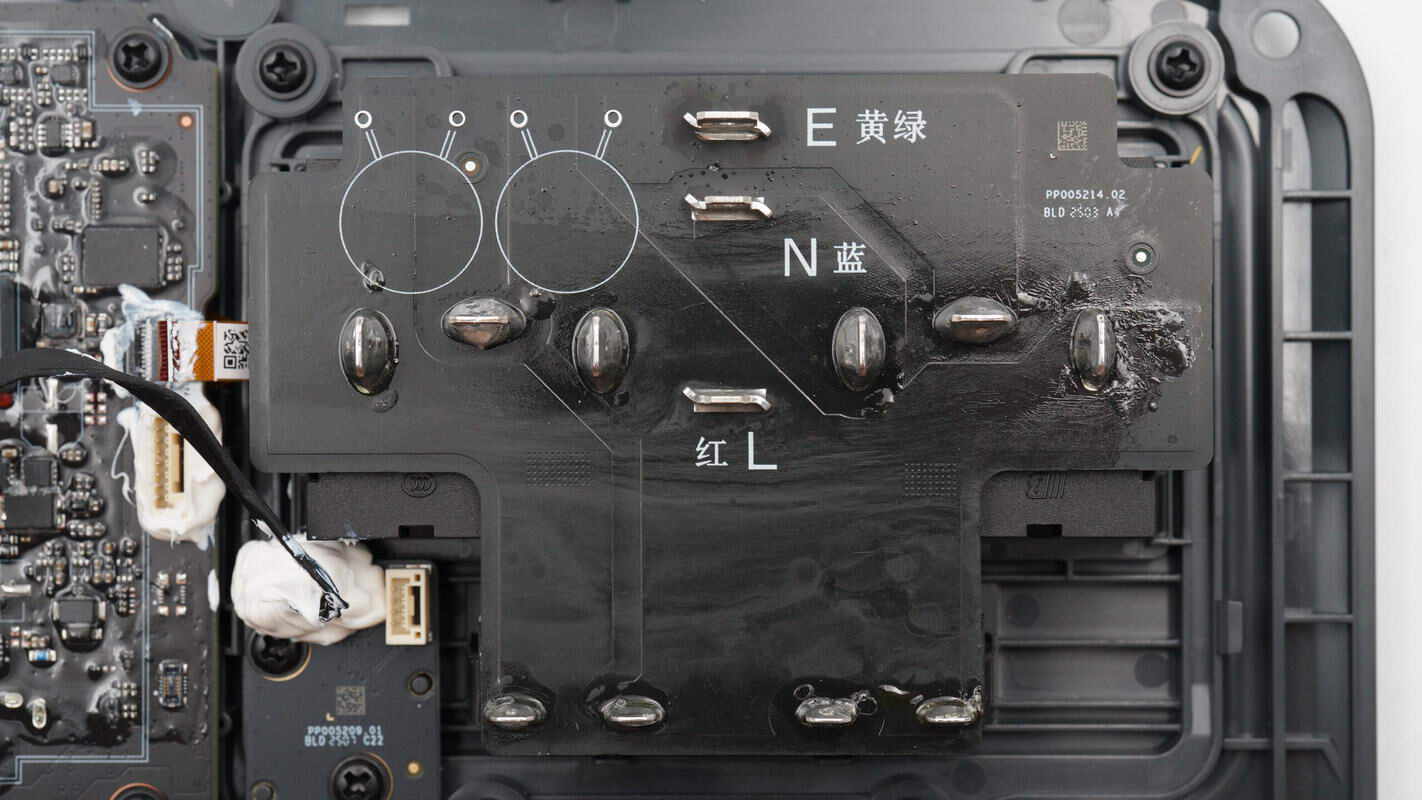
The AC input socket is connected via PCB soldering, with a charging mode switch located below it.
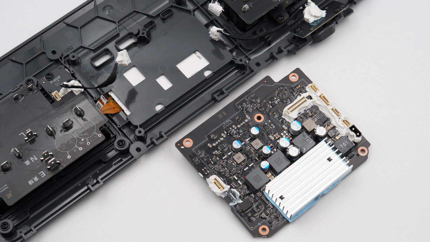
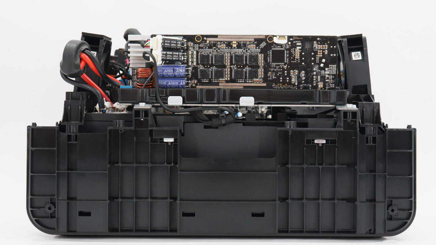
Unscrew the screws, disconnect the wires, and remove the PCBA module from the panel.
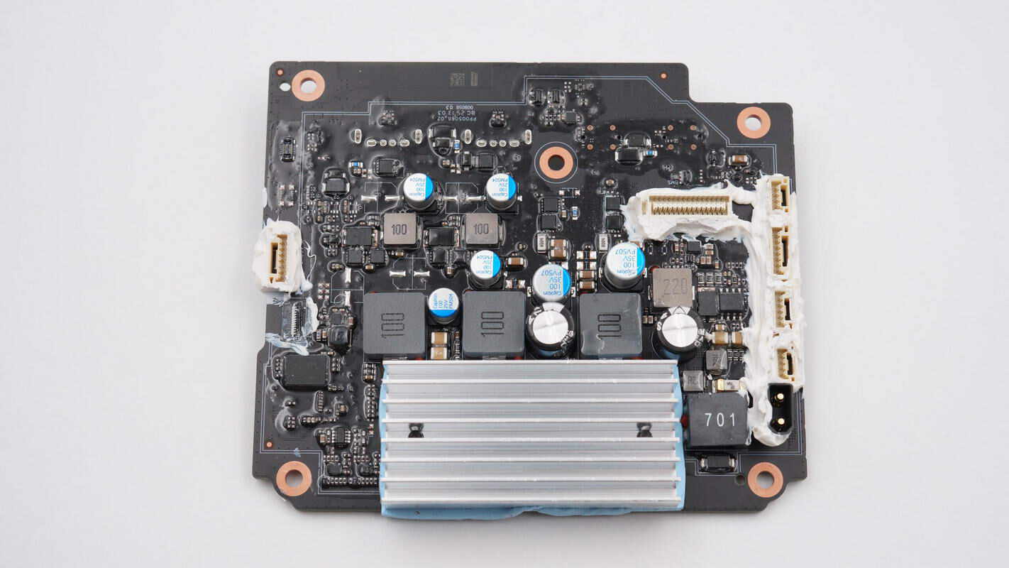
The PCB is equipped with an alloy inductor and filter capacitors, with a heat sink installed underneath.
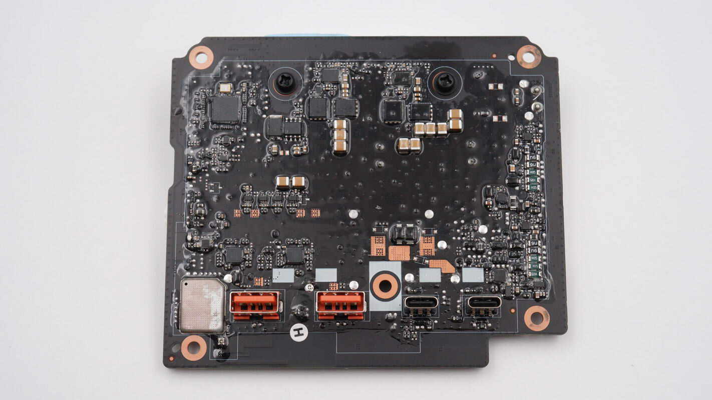
The back contains the MCU, synchronous buck controllers, buck MOSFETs, and USB-A and USB-C sockets.
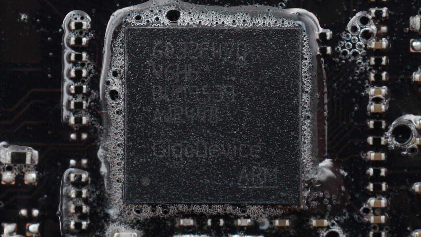
The MCU is from GigaDevice, model GD32F470VGH6. It features a Cortex-M4 core running at 240 MHz, with built-in FPU and DSP. It includes 1 MB of FLASH and 512 KB of SRAM, supports comprehensive communication interfaces, and comes in a BGA100 package.
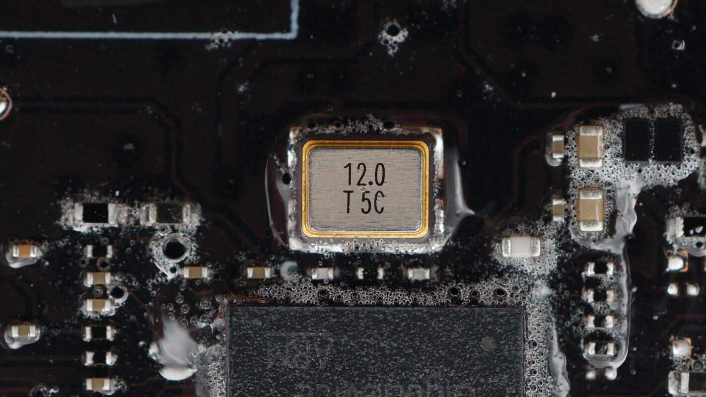
A close-up of the 12.0 MHz clock crystal oscillator.
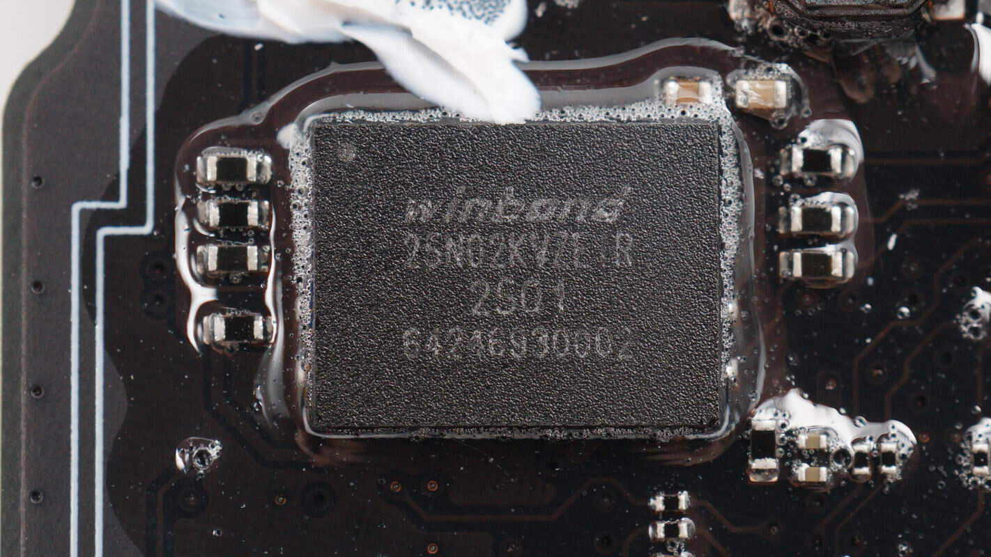
The memory chip is from Winbond, model W25N02KVZEIR, with a capacity of 256MB. It features built-in SLC flash memory and uses a WSON-8 package.
The RS485 transceiver is from 3PEAK, model TPT75176H.
There are two protocol chips located next to the USB-A port.
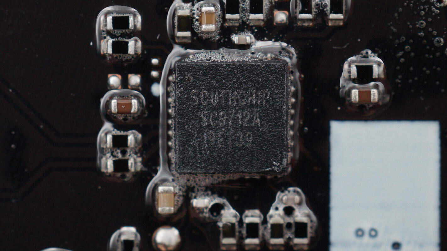
The protocol chip is from SouthChip, model SC9712A. It is a dual-port fast charging protocol chip with an integrated synchronous buck controller. It supports USB PD fast charging and multiple fast charging protocols, accepts 36V input voltage and 7A output current, and supports 140W fast charging output. The switching frequency is adjustable from 80 to 600 kHz. It features output over-voltage protection, under-voltage protection, over-current protection, short-circuit protection, overheating protection, and other protective functions. It supports external resistor settings for output power and fast charging output display. The package type is QFN32.
Inside the heatsink, there is a synchronous buck controller and a buck MOSFET.
The synchronous buck controller for the USB-C port also uses the JOULWATT JWH6346.
The synchronous buck MOSFET comes from Vergiga, model VSP011N10MS-G.
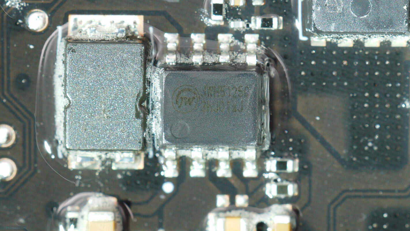
The buck converter is from JOULWATT, model JWH5125C. It has a built-in NMOS, supports an input voltage range of 4.5–65V, and an output current of 5A. The switching frequency and undervoltage protection are configurable. It also features overcurrent protection, short-circuit protection, and overtemperature protection.
Here is the information about JOULWATT JWH5125C.
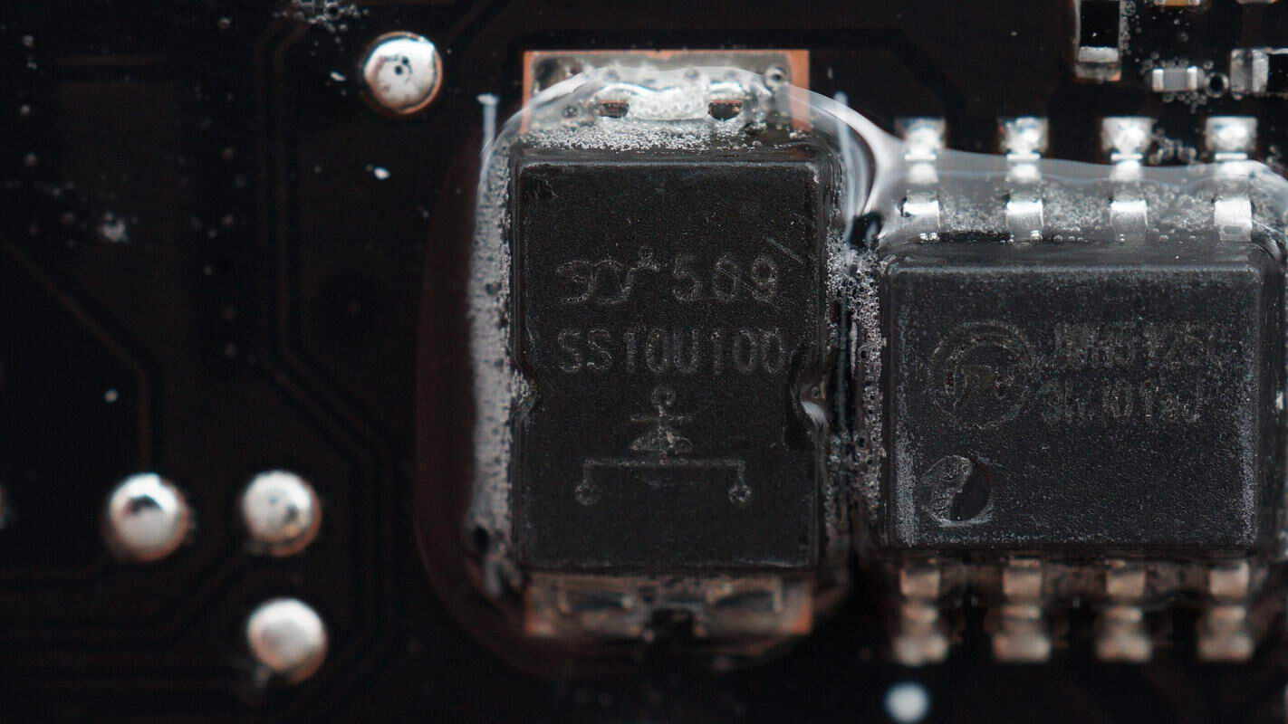
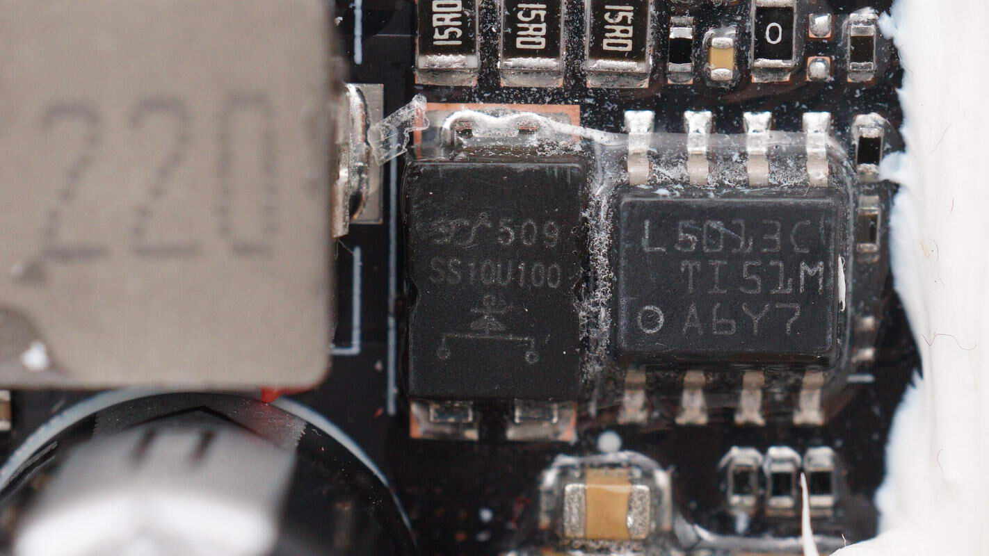
The external Schottky diode is from YJ, model SS10U100, rated at 10A 100V, and uses a TO-277 package.
Three 10μH alloy inductors are used respectively for the two USB-C buck output circuits and the USB-A buck power supply circuit.
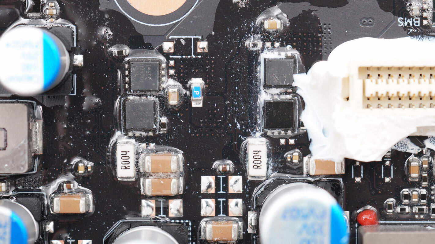
Four VBUS MOSFETs are used to control the output of the two USB-C ports.
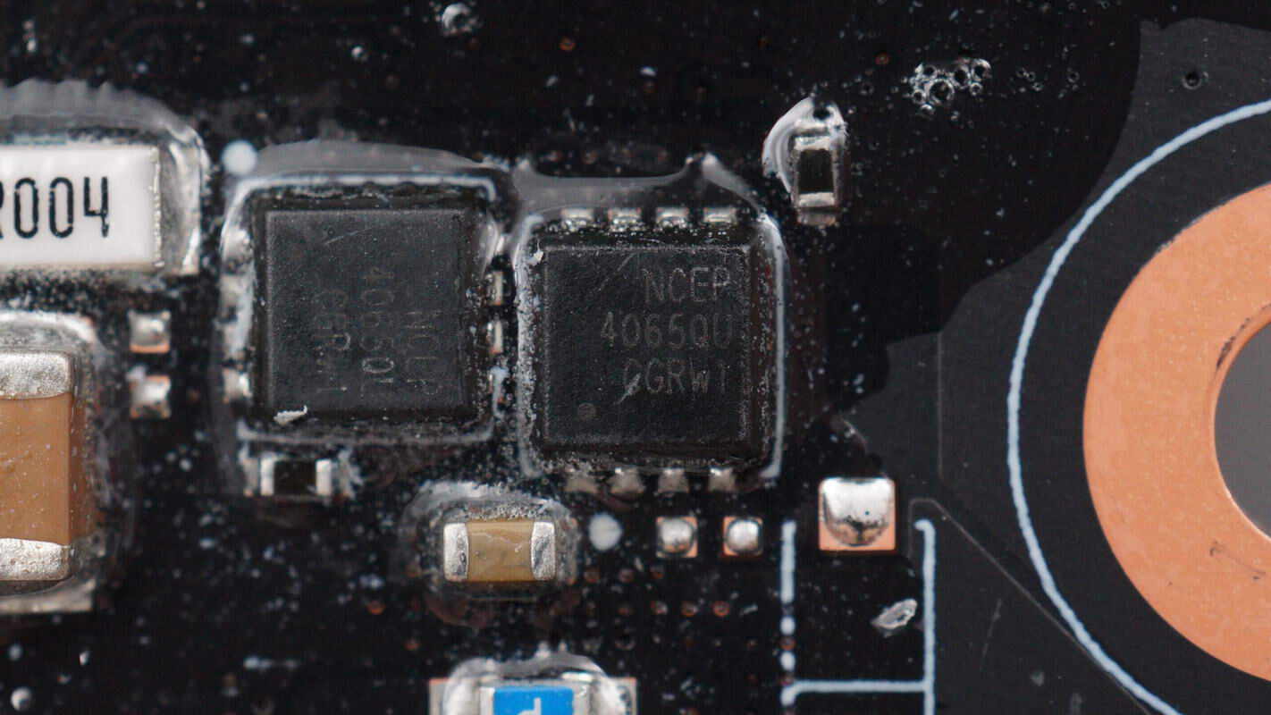
The VBUS MOSFETs come from NCE, model NCEP4065QU. They are NMOS transistors with a 40V voltage rating and 2.2mΩ on-resistance, packaged in DFN 3.3×3.3 mm.
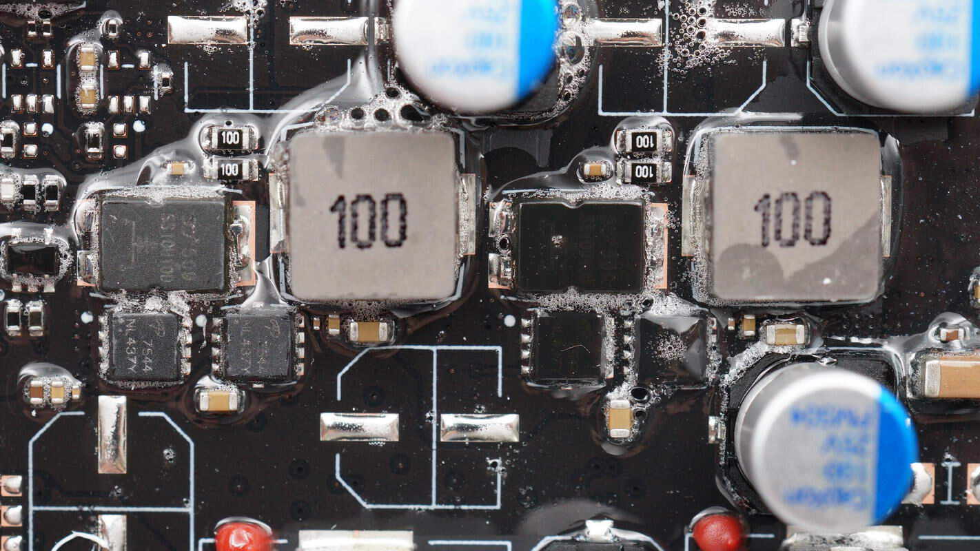
Close-up of the buck MOSFET and the buck inductor used for the USB-A port..
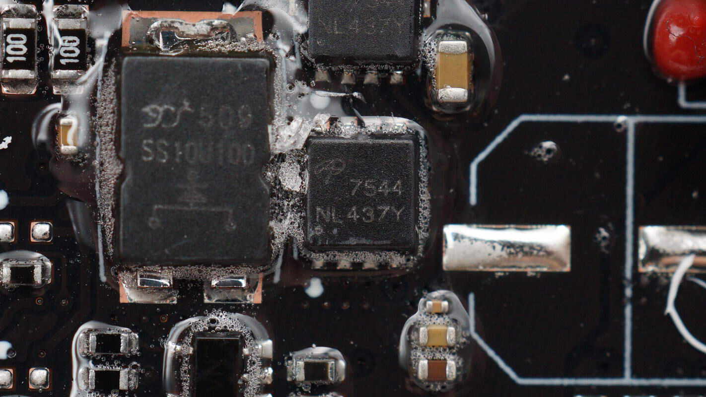
The synchronous buck MOSFET is from AOS, model AON7544. It is an NMOS with a 30V voltage rating and a 4.1mΩ on-resistance. It features low gate charge and high current capability, packaged in a DFN 3×3 EP.
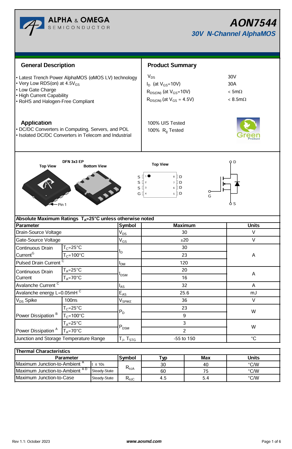
Here is the information about AOS AON7544.
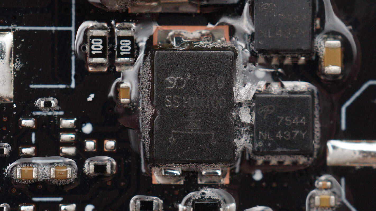
The external Schottky diode is from YJ, model SS10U100.
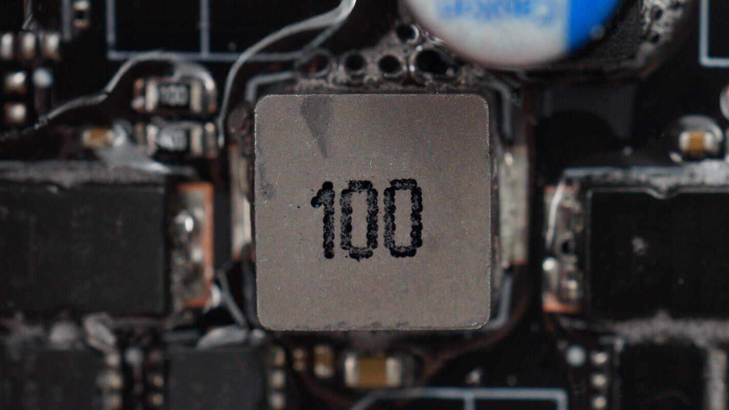
Close-up of the 10μH buck inductor.
The VBUS MOSFET uses the NCE NCEP4065QU model.
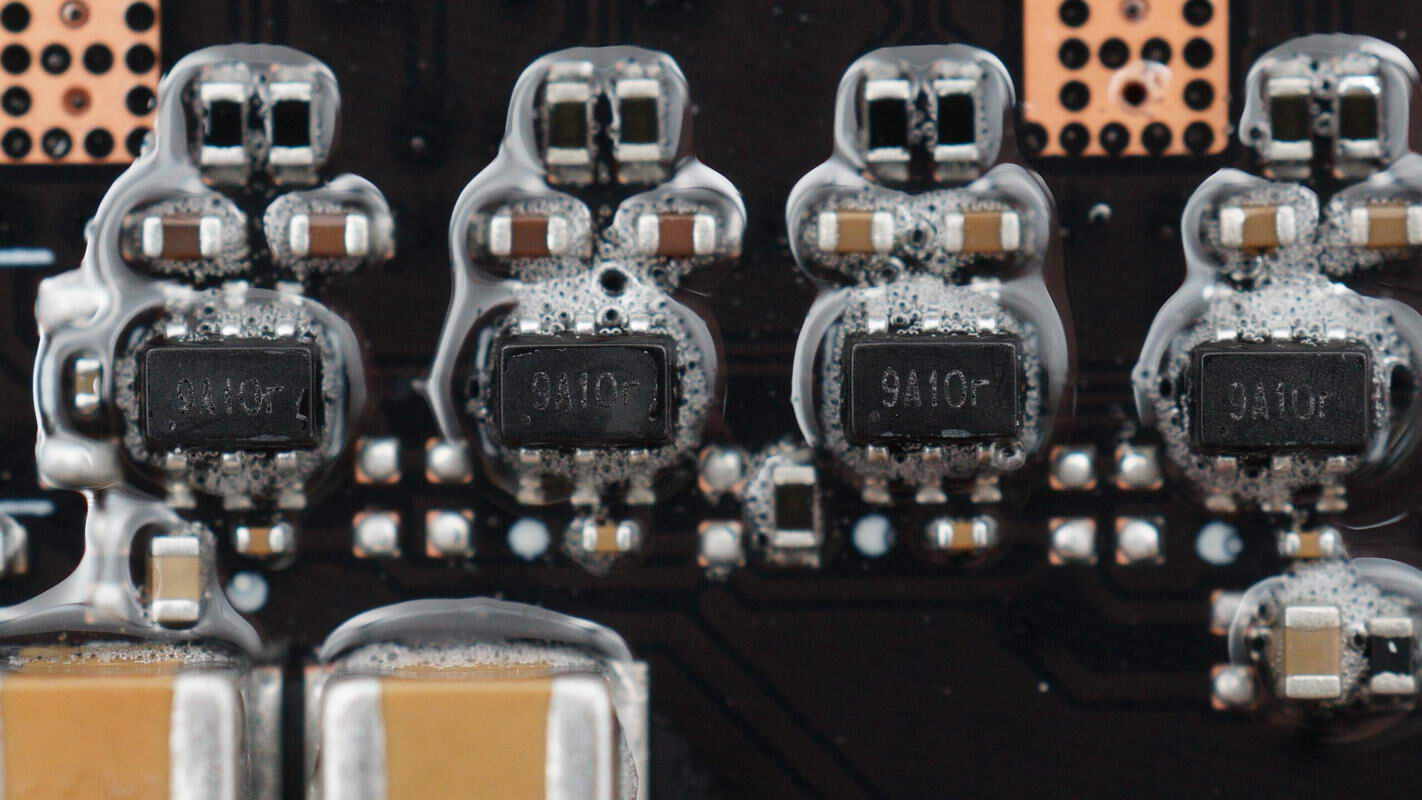
The current sensing chip is from 3PEAK, marked with 9A1, model TP181A1. It is a zero-drift, bidirectional current sense amplifier, packaged in SC70.
Close-up of the XT30 power input connector.
Close-up of the SMD common mode choke.
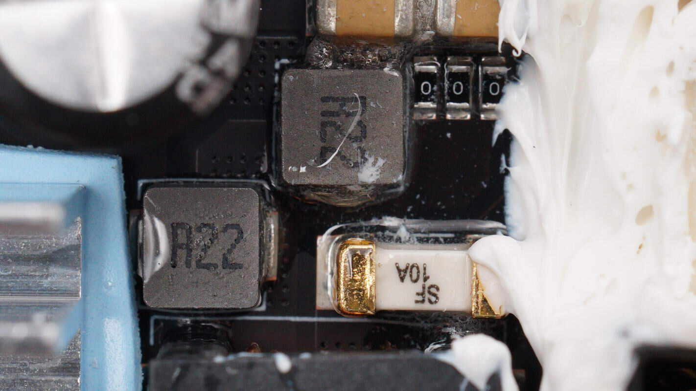
Close-up of the input side 10A SMD fuse and two 0.22μH filter inductors.
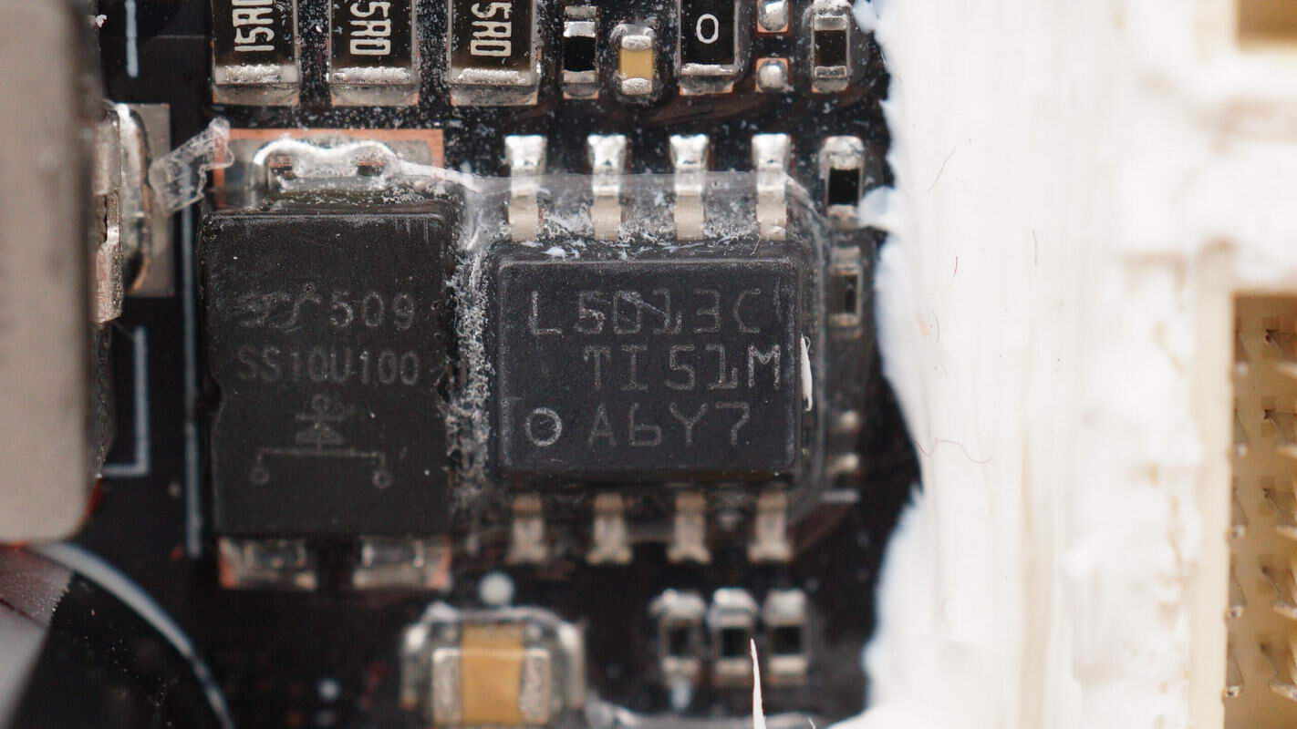
The buck chip is from TI, marked with L5013C, model LM5013. It supports 100V input voltage and 3.5A output current, features ultra-low quiescent current, and comes in an HSOIC8 package..
The external Schottky diode is from YJ, model SS10U100.
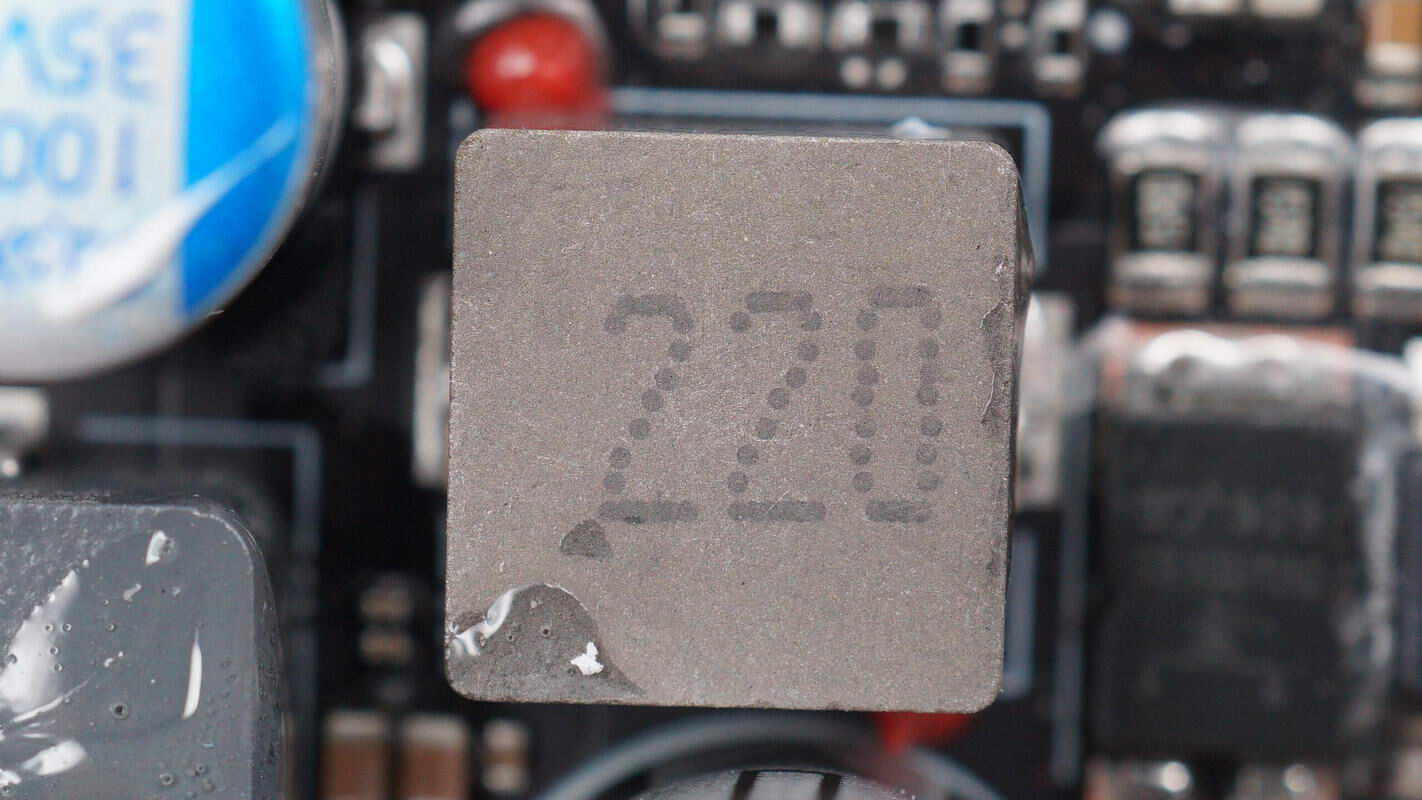
Close-up of the 22 μH alloy inductor.
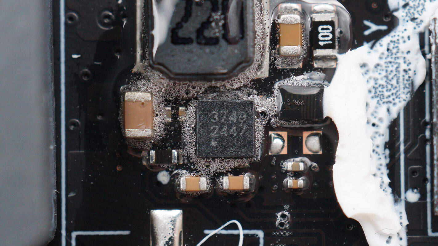
The screen backlight driver chip is from SGMICRO, model SGM3749. It is a boost LED driver that supports PWM dimming. The chip supports an input voltage of up to 20V, operates at a switching frequency of 1.25MHz, and comes in a TDFN2×2-6L package.
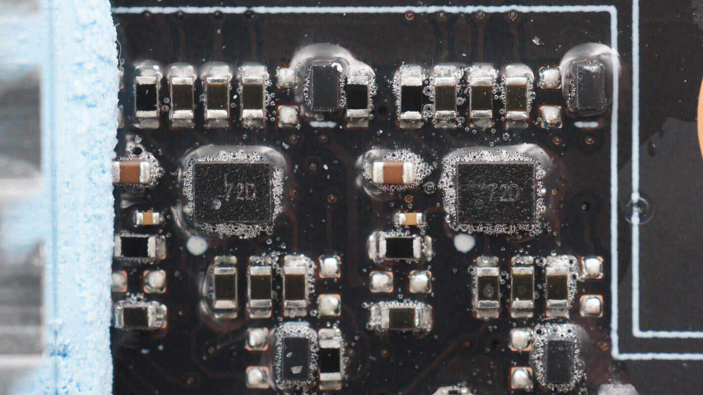
Two switching chips are marked with 72D.
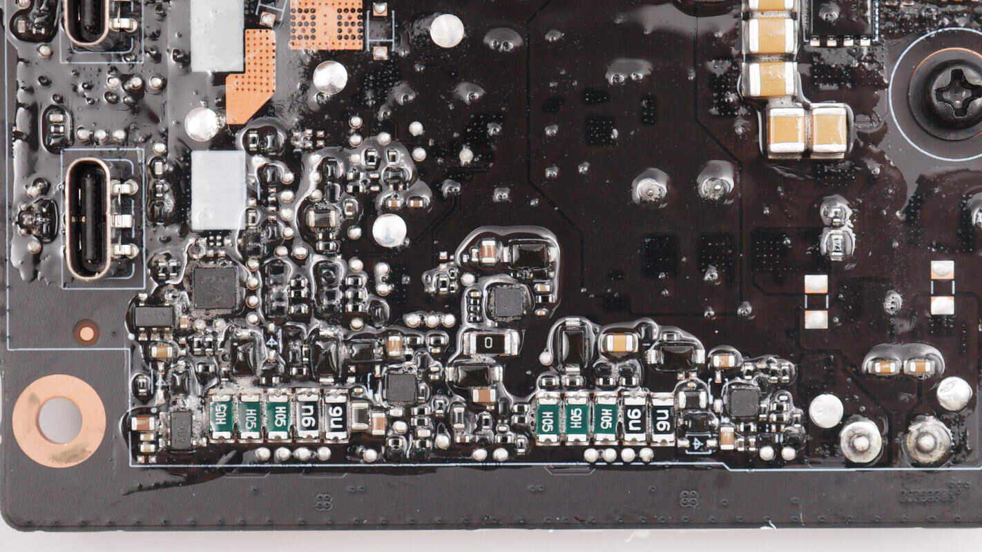
At the edge of the PCBA module, there are components such as a resettable fuse, overcurrent protection chip, and voltage regulator.
The overcurrent protection chip is from ETA, model ETA6027. It supports up to 6V input, has 6.1V overvoltage protection, a current limit from 75mA to 2.2A, supports fast overcurrent protection, reverse current blocking, thermal shutdown, and undervoltage protection. It uses a DFN2×2-6 package.
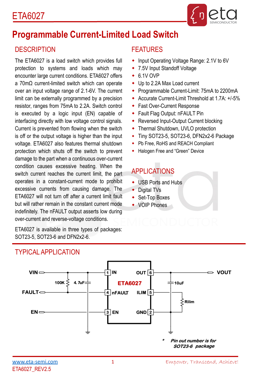
Here is the information about ETA ETA6027.
Another overcurrent protection chip has the same model.
Two voltage regulator chips are from ETA, marked with fv, model ETA5044V330NS2F. They support an input voltage of up to 45V, output current of 300mA, feature ultra-low quiescent current, and come in a SOT23-5 package.
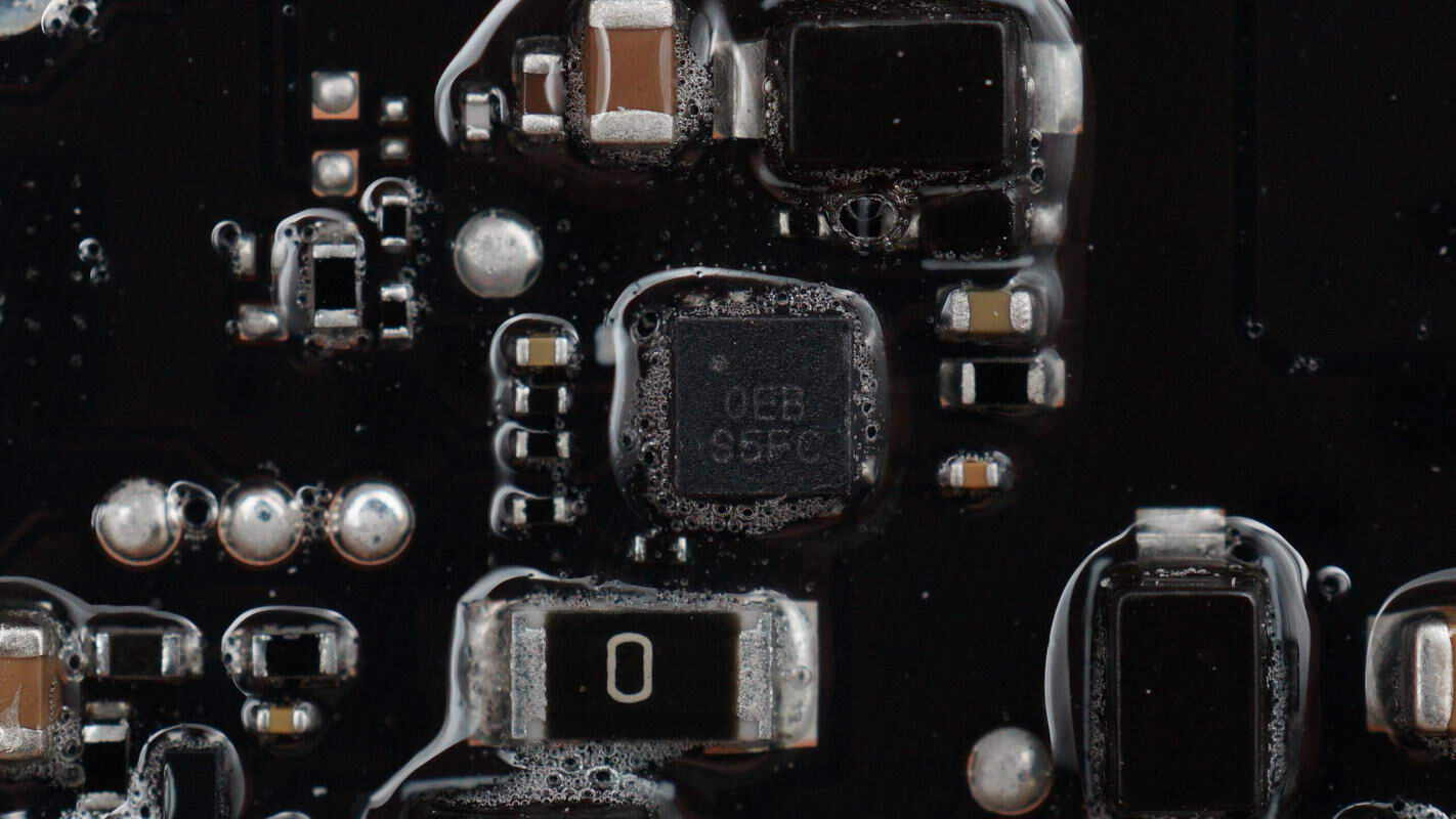
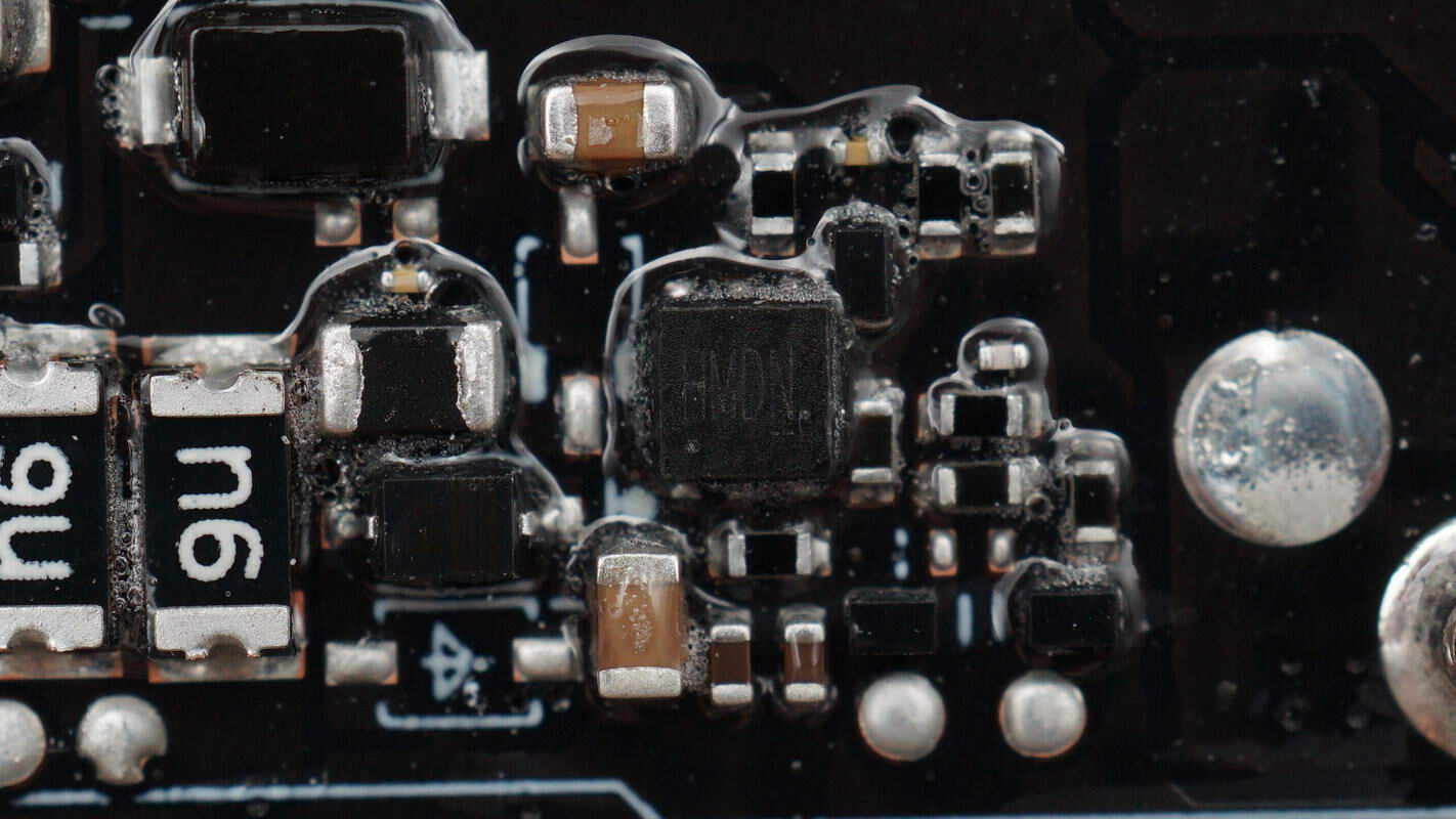
Close-up of the chip marked with 0EB S5FC.
Close-up of the fuses used for overcurrent protection.
Close-up of another set of fuses.
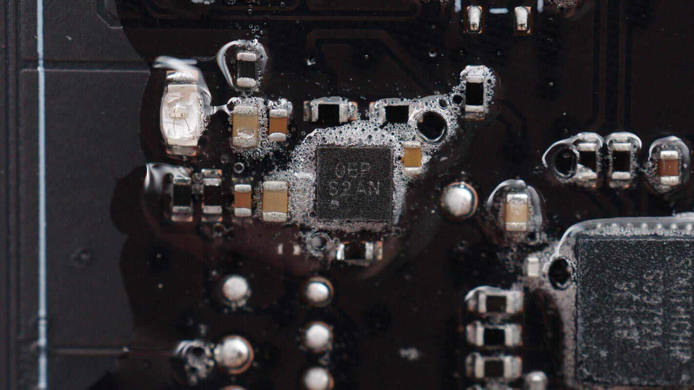
Close-up of the chip marked with 0EP S2AN.
Close-up of the onboard wireless communication antenna.
The USB-A sockets use through-hole soldering.
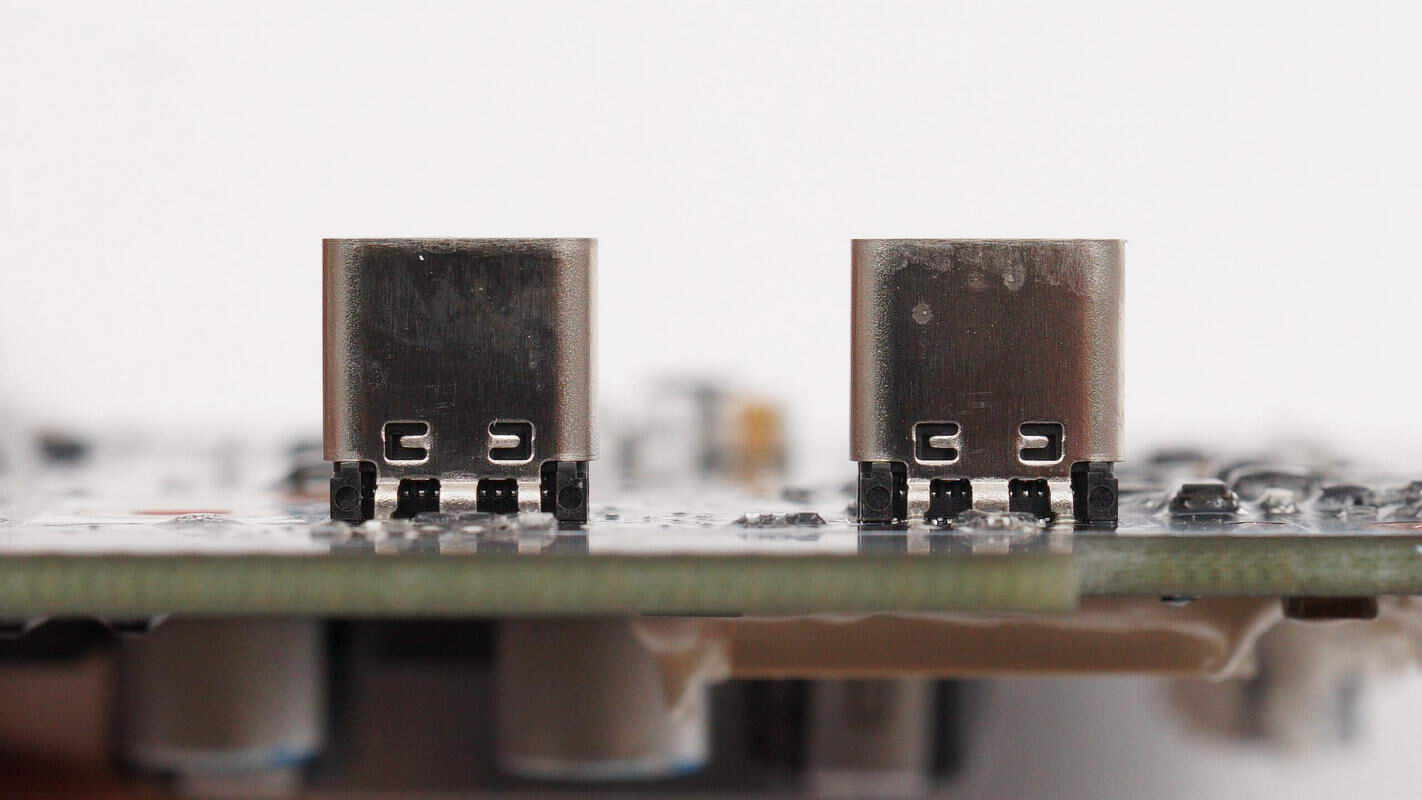
The USB-C sockets also use through-hole soldering.

Well, those are all components of the DJI 2600W 1024Wh Power 1000 V2 Portable Power Station.
Summary of ChargerLAB
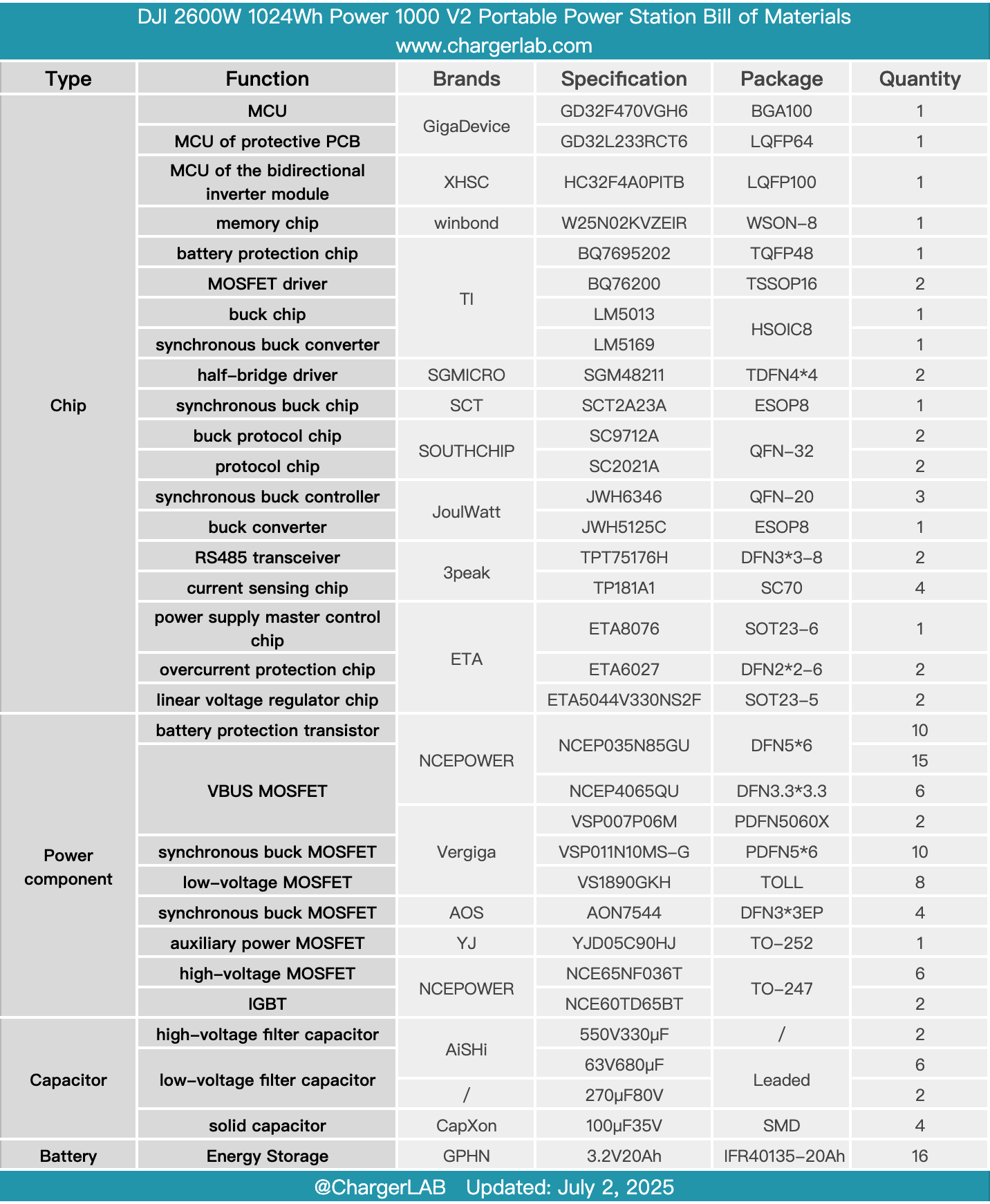
Here is the component list of the DJI 2600W 1024Wh Power 1000 V2 Portable Power Station for your convenience.
It features integrated handles on both sides. The front panel includes a screen, USB ports, AC input/output ports, and SDC ports. It has a built-in 1024Wh lithium iron phosphate battery and supports a 2600W inverter output. The USB-C port supports 140W fast charging, and the SDC port supports charging the power station as well as output and connection to additional power packs.
After taking it apart, we found that it features a modular design, consisting of a display panel, a battery protection PCB, and a bidirectional inverter module. The bottom of the bidirectional inverter module is potted with hard potting compound for protection, with fans on both sides, and a metal baseplate is used for the inverter module. The battery pack is composed of 16-series lithium iron phosphate cells from GPHN, secured with an insulating frame. The battery protection board uses a TI protection chip, paired with a GigaDevice master control chip, and is equipped with multiple fuses for overcurrent protection.
The bidirectional inverter module uses an XHSC master control chip, paired with NCE power components. It is composed of multiple small PCBs to maximize space efficiency. The display panel is controlled by a GigaDevice chip, working alongside a SouthChip protocol chip and a JOULWATT synchronous buck controller. It also features ETA overcurrent protection and linear voltage regulator chips. The internal construction is precise and well-built, with high-quality components. The PCBs are coated and sealed, and the inverter module is potted for enhanced protection, ensuring reliable and safe power usage.
Related Articles:
1. Teardown of HUAWEI 100W SuperCharge Car Charger (P0019)
2. Teardown of Nintendo Switch 2 Official Charging Dock
3. Teardown of SHARGE Pixel 140 GaN Charger (S2)