Introduction
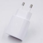
CUKTECH has launched a brand-new fast charging product — the CP6 GaN Charger with Retractable Cable. It features a 0.7-meter USB-C cable, along with one USB-A and one USB-C port. The charger supports 65W Power Delivery and Xiaomi 67W Turbo fast charging.
The built-in retractable USB-C cable is a major highlight, offering adjustable length for a tidy desktop setup. It’s also travel-friendly, eliminating the need to carry an extra cable. The retractable mechanism uses a high-precision alloy hinge that ensures smooth and quiet operation. Let’s take a closer look at the design of this charger.
Product Appearance
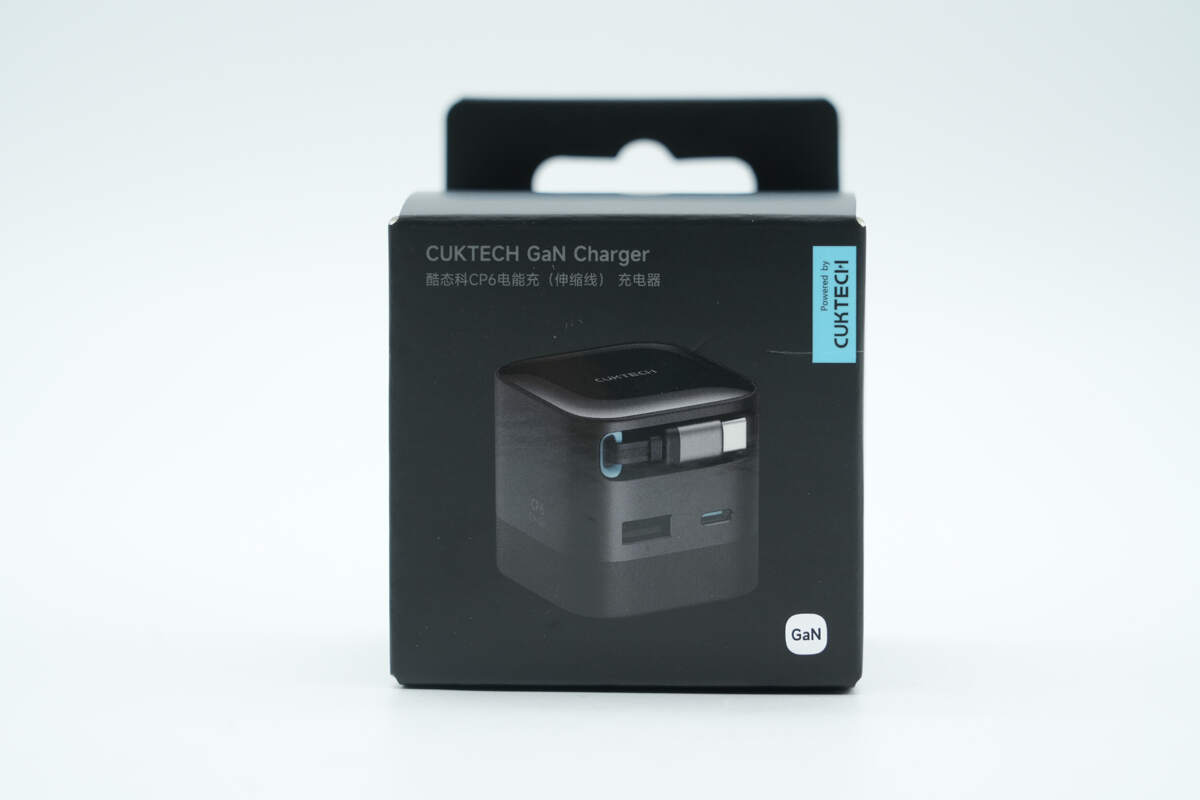
The front of the packaging displays the product name, its appearance, and the phrase “Powered by CUKTECH.” In the bottom right corner, there’s also a GaN badge.

The back of the packaging features usage scenarios, key selling points, and spec information.
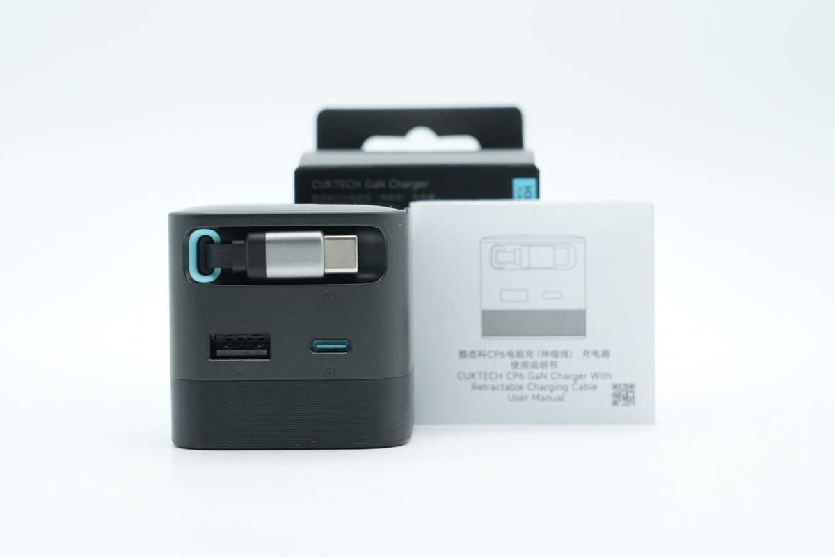
The package includes the charger and a user manual.
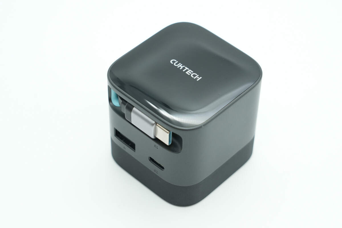
It features a rectangular column design with a flame-retardant shell, combining glossy and matte finishes.
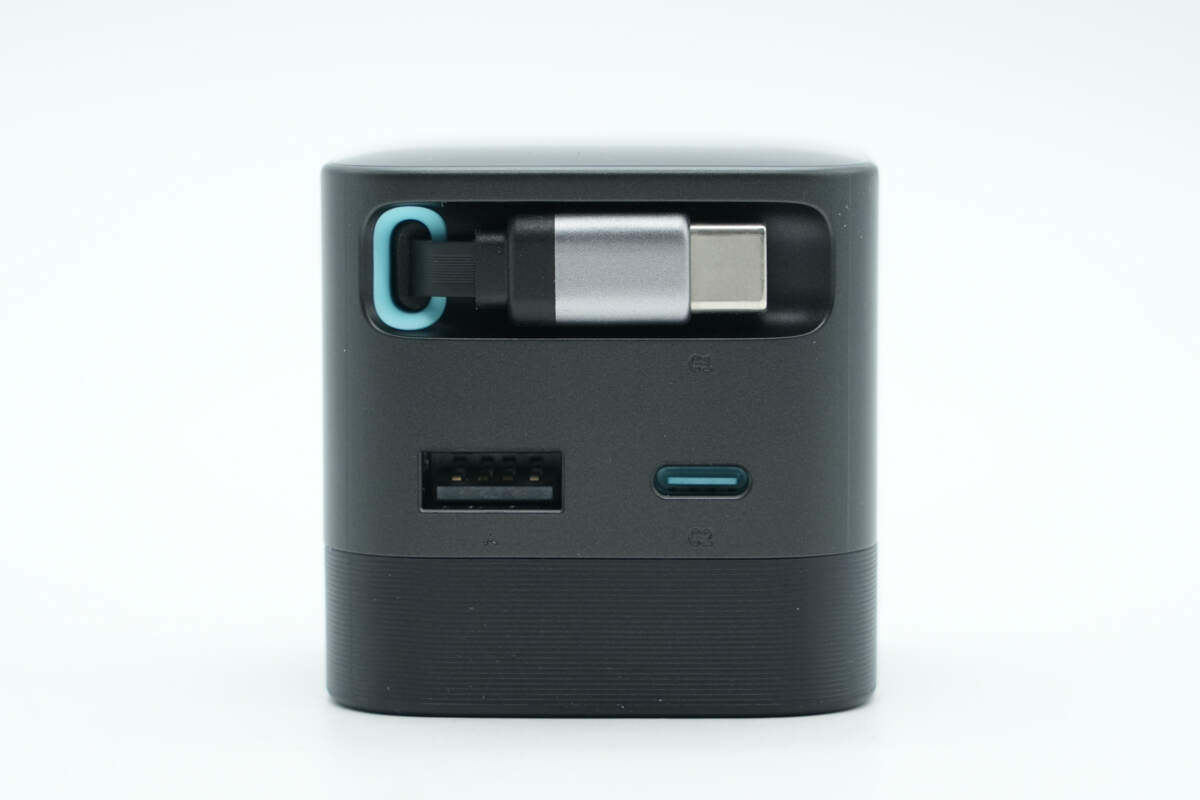
The front is equipped with the USB-C retractable cable as well as a USB-A and a USB-C port.
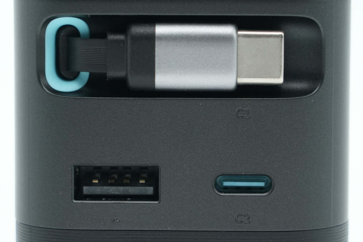
The ports are marked with C1, C2, and A.
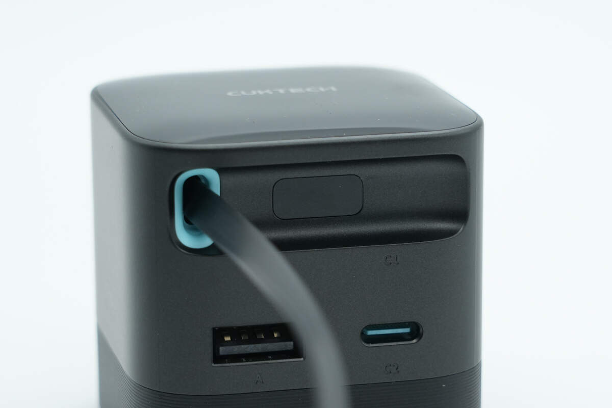
A magnet is located inside the cable slot to secure the USB-C connector in place.
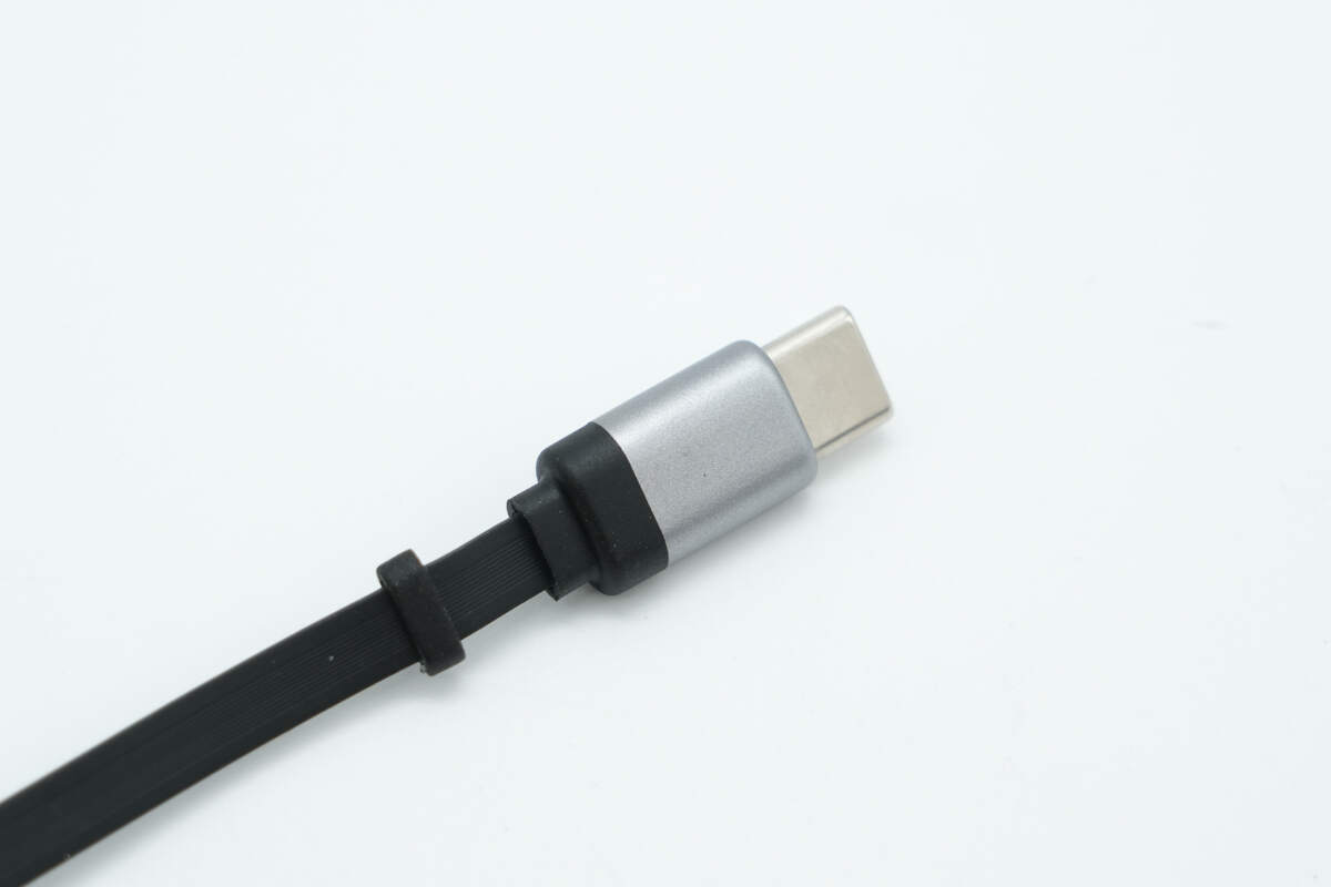
The connector features a metal housing with smooth, rounded edges.
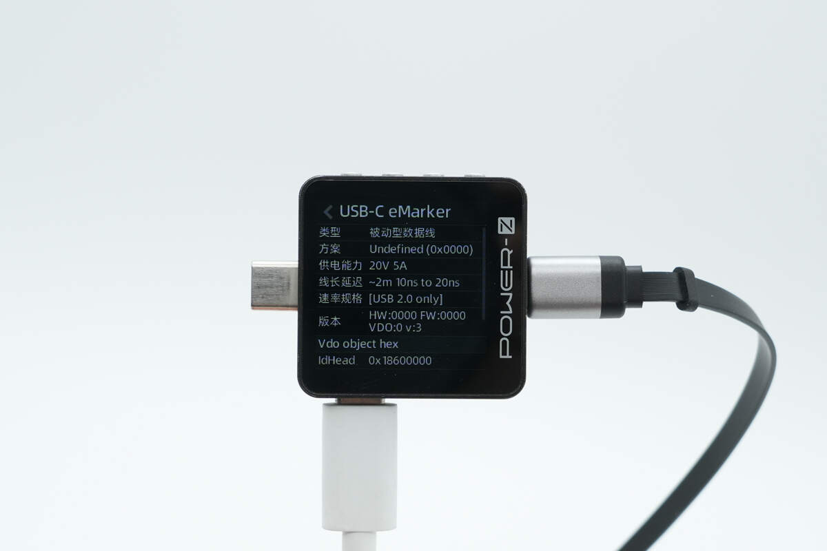
ChargerLAB POWER-Z KM003C shows that it has an E-Marker chip, with a power delivery capability of 20V5A and data transfer capability of USB 2.0.
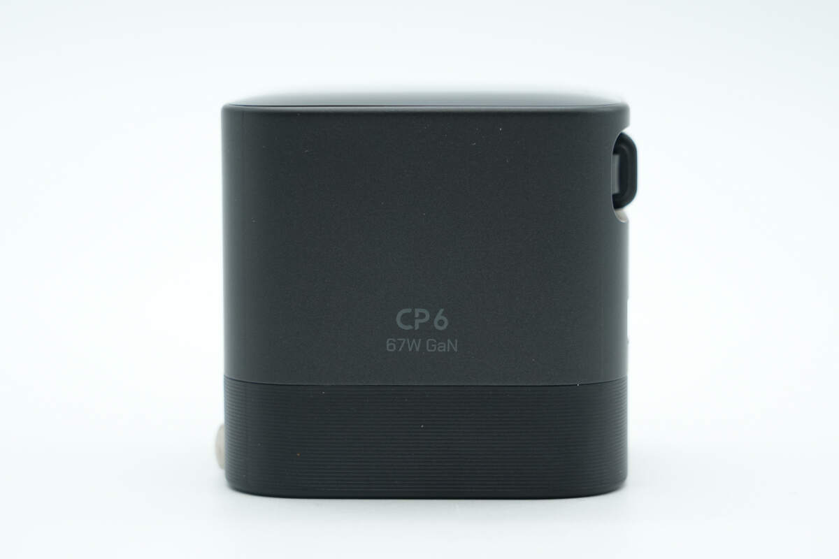
"CP6" and "67W GaN" are printed on the side.
There is CUKTECH at the top center.
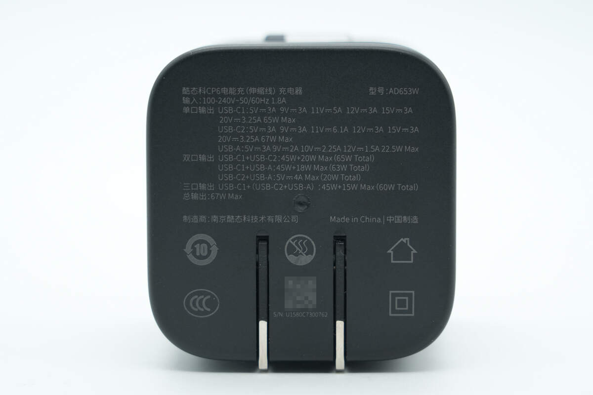
Spec info is printed on the bottom.

Model: AD653W
Input: 100-240V\~ 50/60Hz 1.8A
Single-port output
USB-C1: 5V⎓3A, 9V⎓3A, 11V⎓5A, 12V⎓3A, 15V⎓3A, 20V⎓3.25A 65W Max
USB-C2: 5V⎓3A, 9V⎓3A, 11V⎓6.1A, 12V⎓3A, 15V⎓3A, 20V⎓3.25A 67W Max
USB-A: 5V⎓3A, 9V⎓2A, 10V⎓2.25A, 12V⎓1.5A 22.5W Max
Dual-port output
USB-C1 + USB-C2: 45W + 20W Max (65W Total)
USB-C1 + USB-A: 45W + 18W Max (63W Total)
USB-C2 + USB-A: 5V⎓4A Max (20W Total)
Three-port output
USB-C1 + (USB-C2 + USB-A): 45W + 15W Max (60W Total)
Total output: 67W Max

It is equipped with a foldable plug.
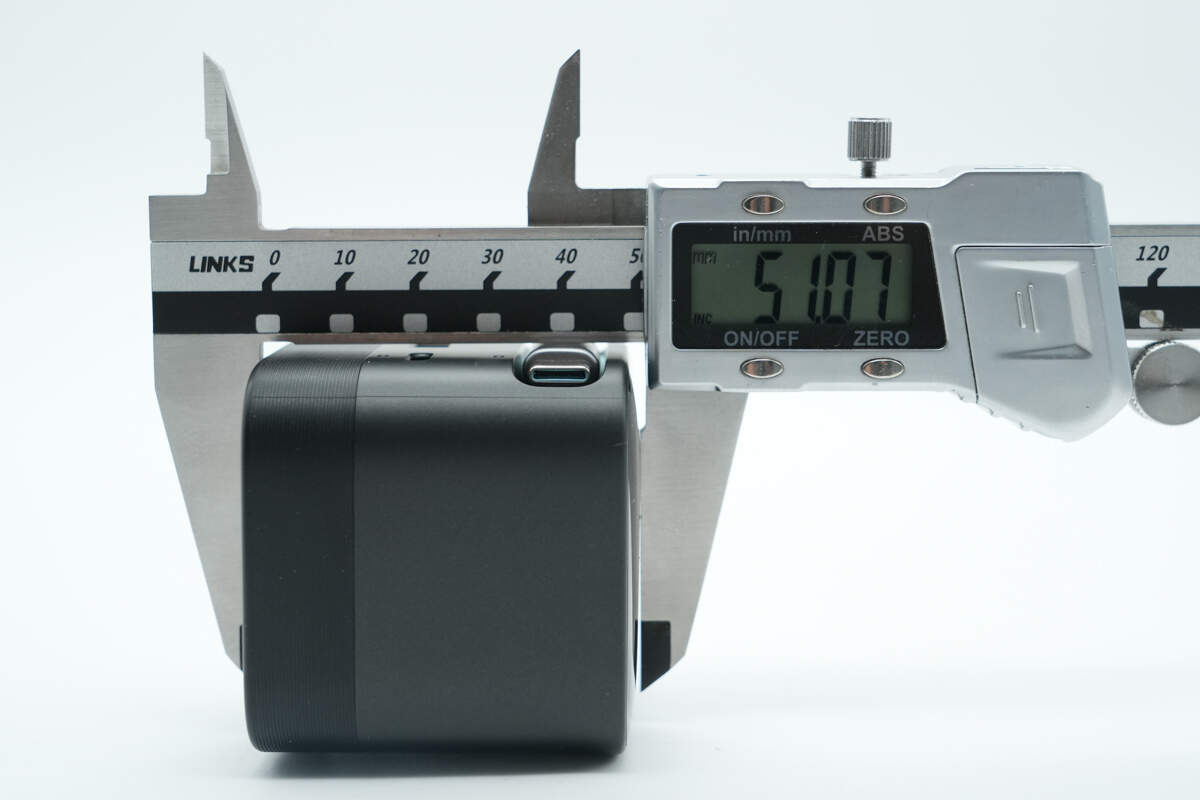
The length of the charger is about 51.07 mm (2.011 inches).
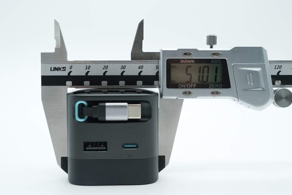
The width is about 51.01 mm (2.0083 inches).
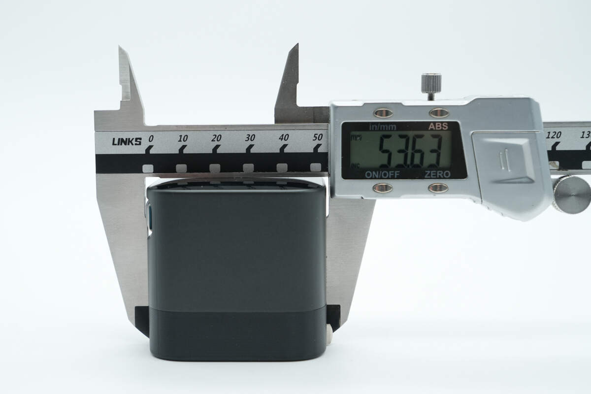
The thickness is about 53.63 mm (2.11 inches).

The length of the cable is about 68 cm (26.77 inches).
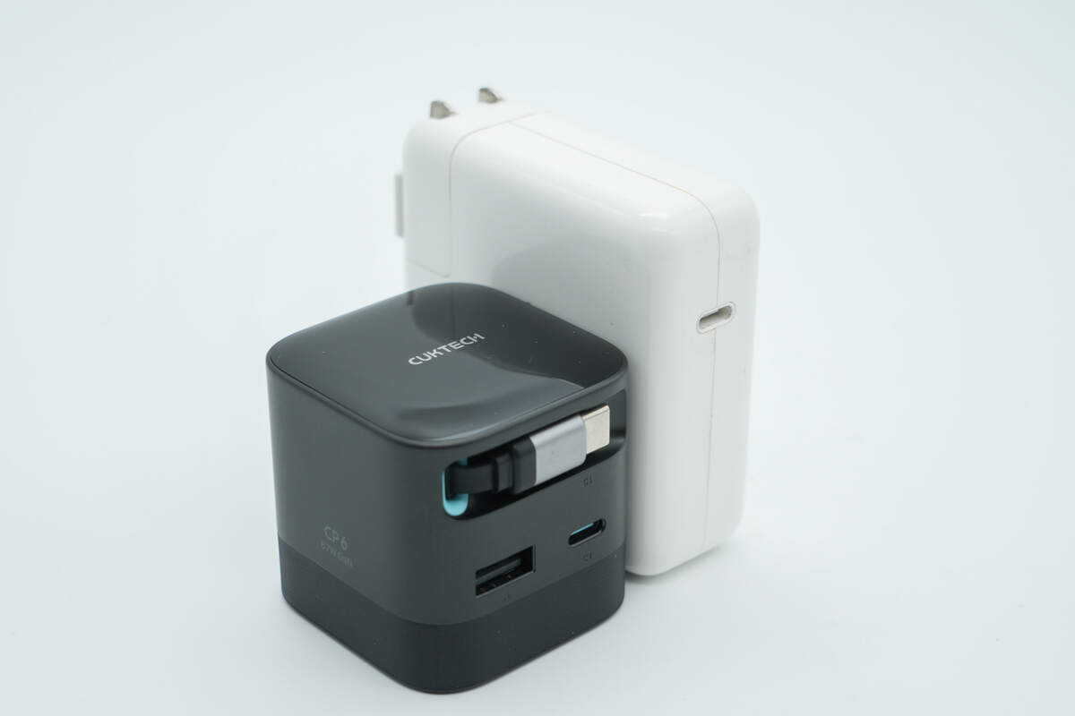
Compare it with the Apple 67W charger.
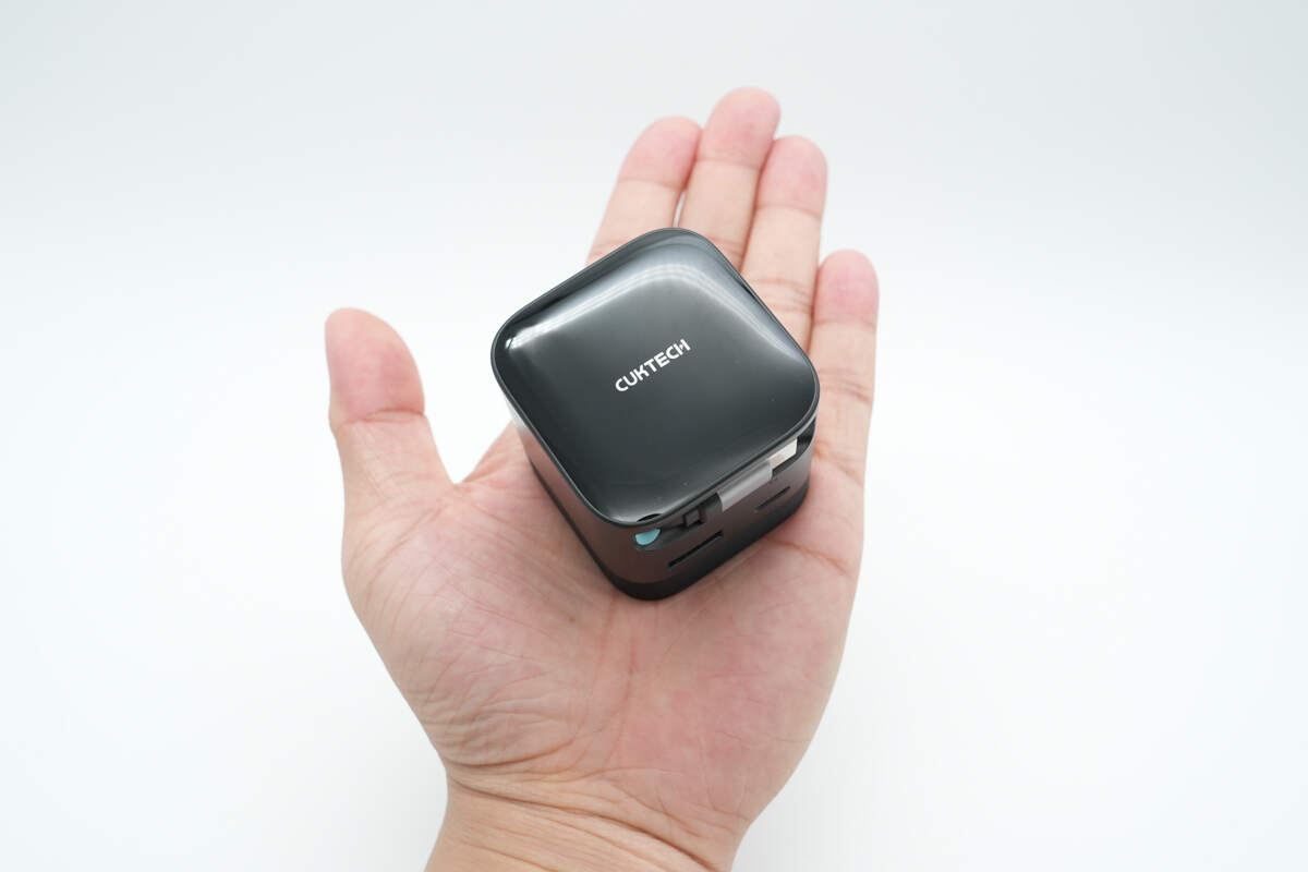
That's how big it is in the hand.
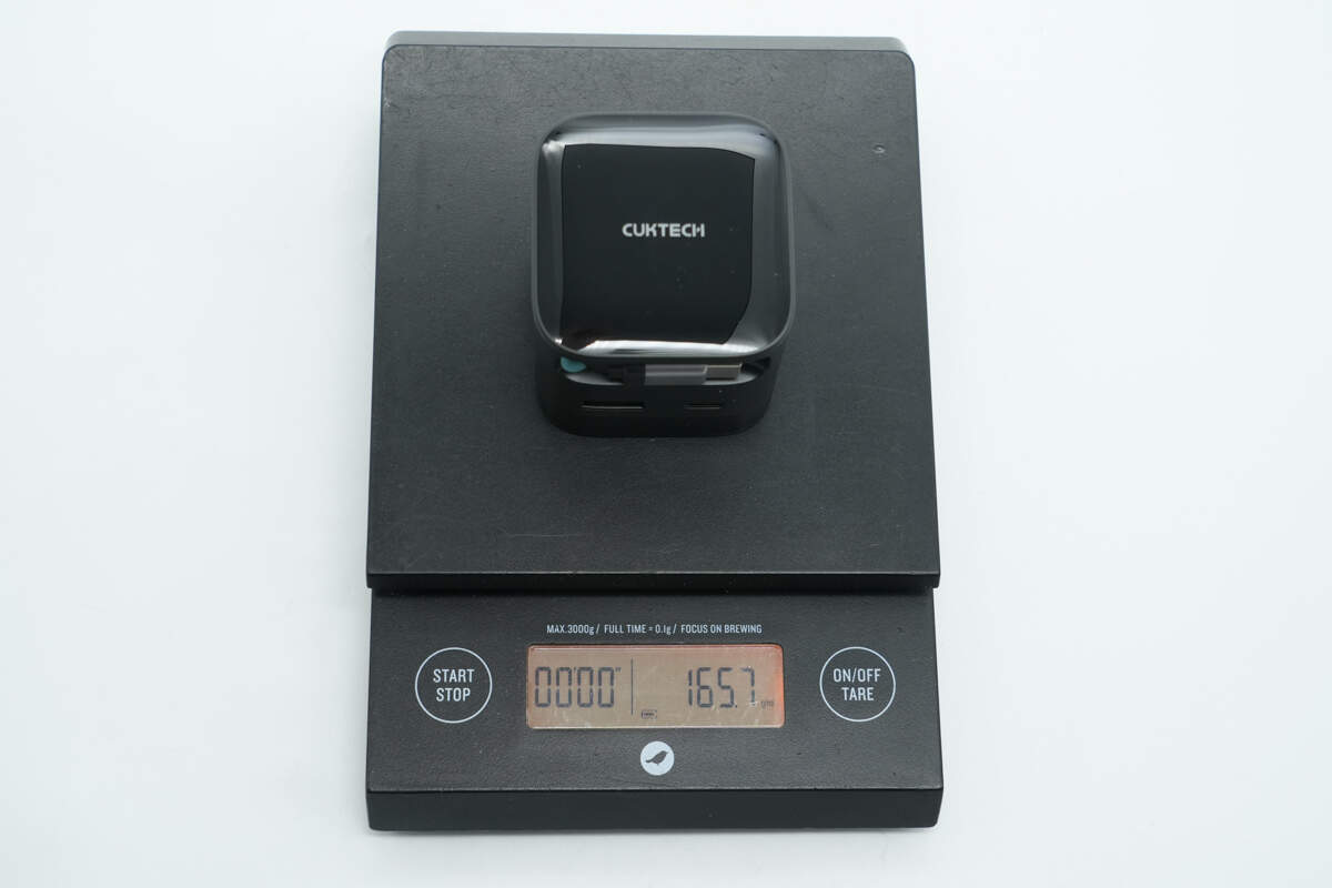
The weight is about 166 g (5.86 oz).
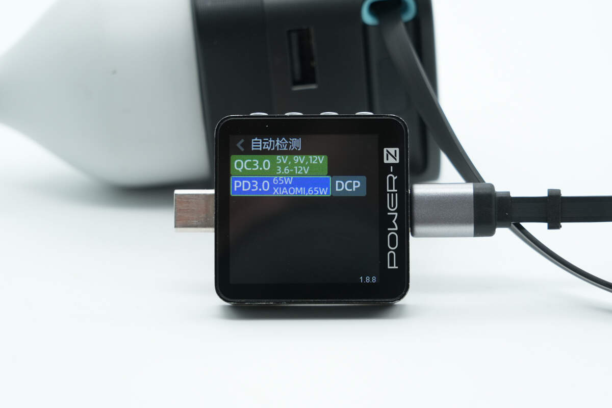
ChargerLAB POWER-Z KM003C shows that the USB-C1 supports QC3.0, PD3.0, and DCP charging protocols, as well as Xiaomi’s proprietary 65W fast-charging protocol.
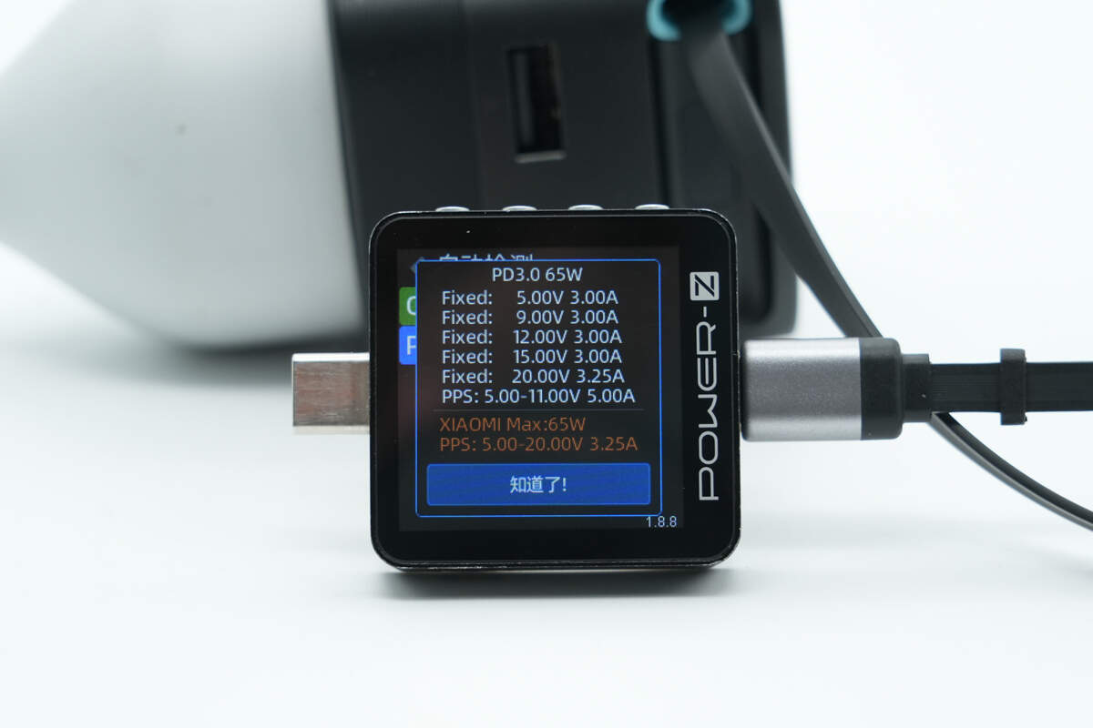
And it has five fixed PDOs of 5V3A, 9V3A, 12V3A, 15V3A, and 20V3.35A, as well as a 5-11V⎓5A PPS voltage range and a 5-20V⎓3.25A Xiaomi proprietary voltage range.
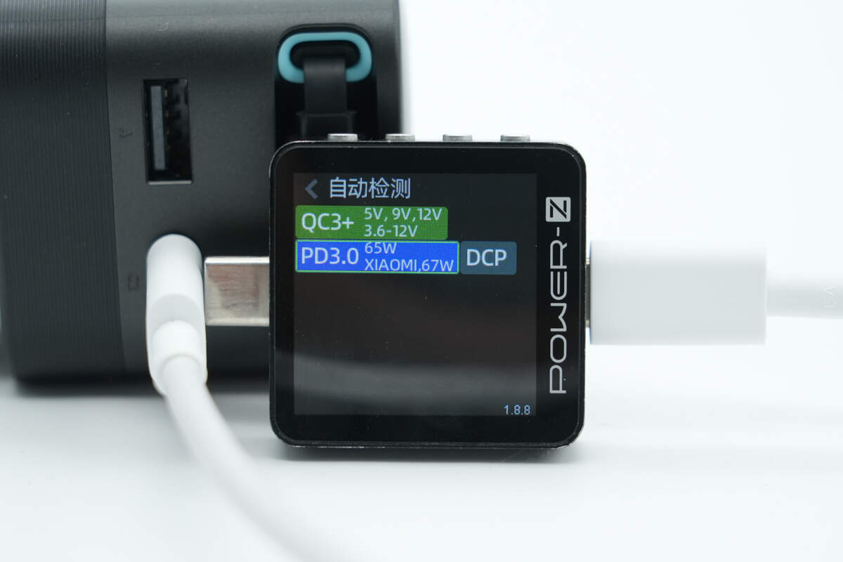
The USB-C2 supports QC3+, PD3.0, and DCP charging protocols, as well as Xiaomi’s proprietary 67W fast-charging protocol.
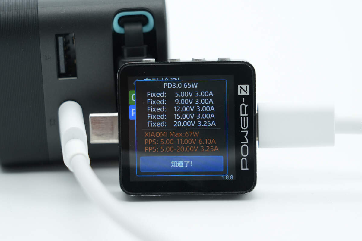
And it has five fixed PDOs of 5V3A, 9V3A, 12V3A, 15V3A, and 20V3.35A, as well as two Xiaomi proprietary voltage ranges: 5-11V⎓6.1A and 5-20V⎓3.25A.
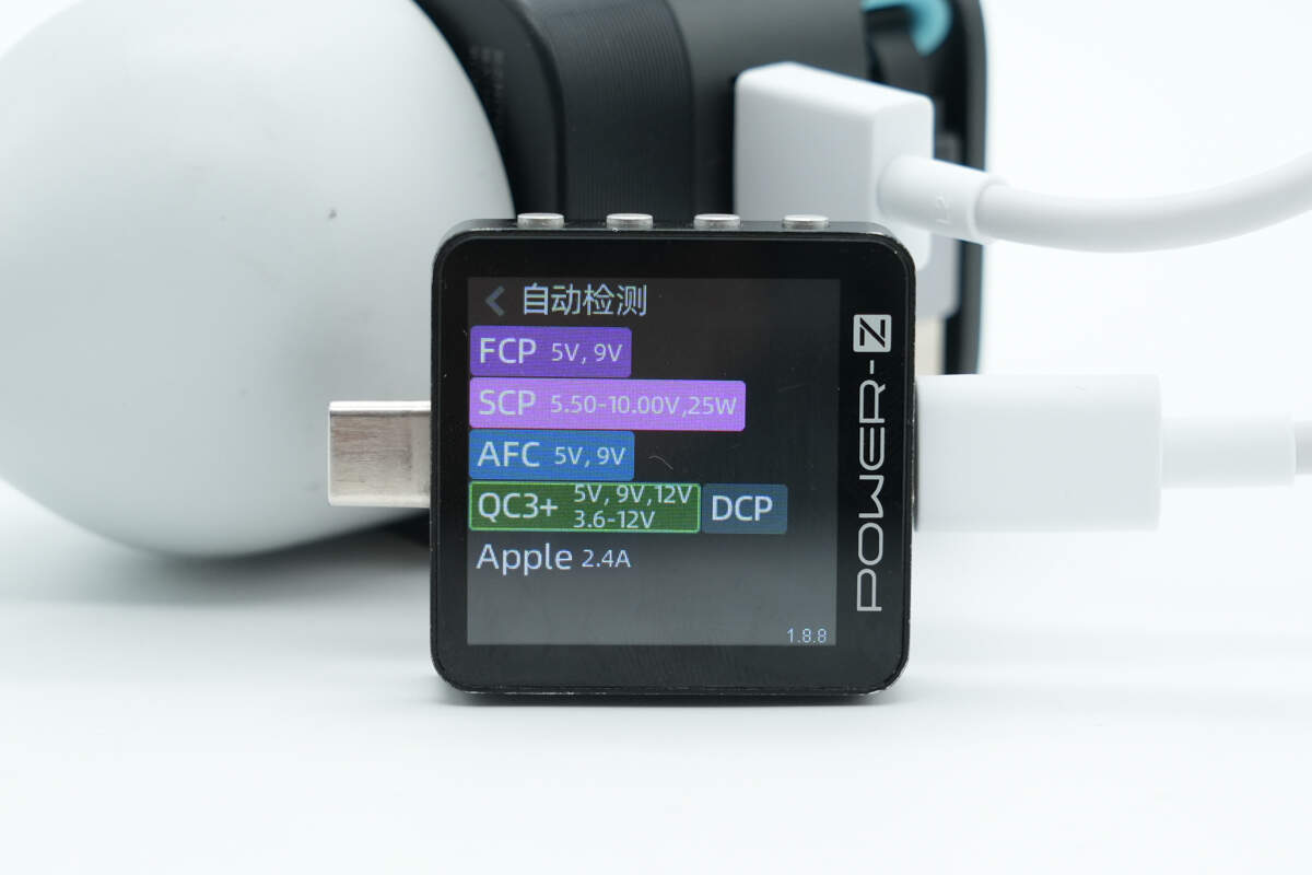
The USB-A supports FCP, SCP, AFC, QC3+, DCP, and Apple 2.4A charging protocols.

Using USB-C2 to charge the Xiaomi 15 Pro successfully activates Xiaomi’s 67W proprietary charging protocol.
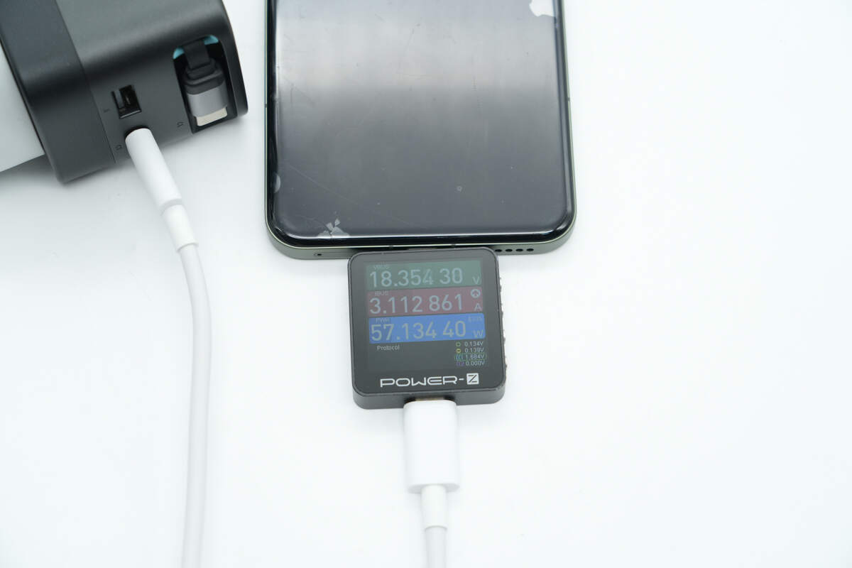
When the charging power ramps up to a stable state, the charging power is about 57.13W.
Teardown
Next, let's take it apart to see its internal components and structure.
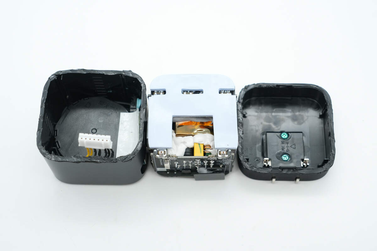
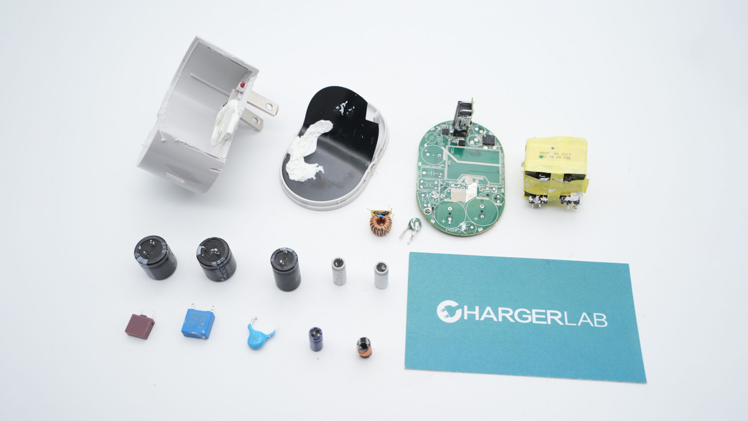
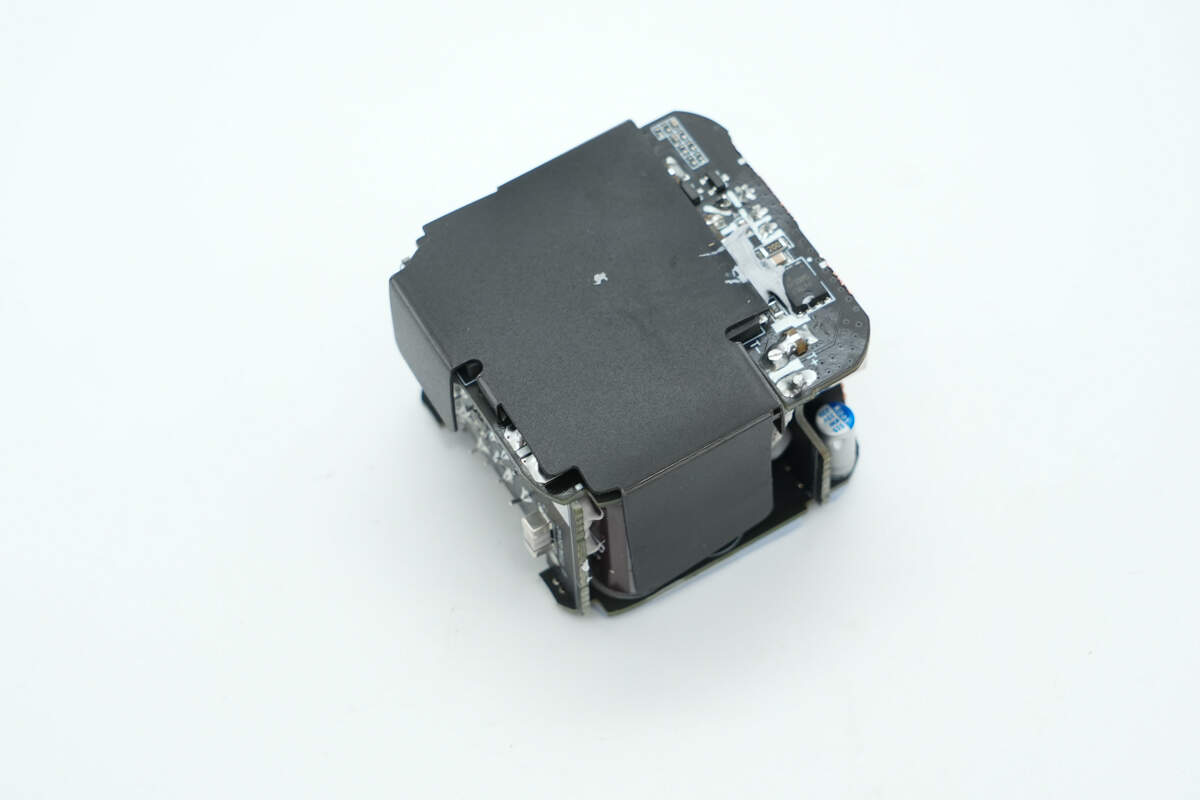
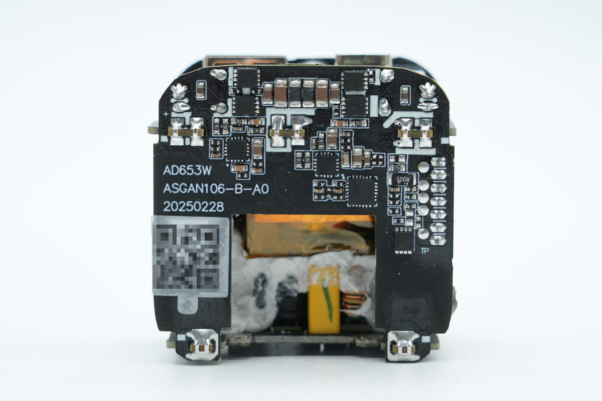
Cut open the shell to remove the PCBA module.

The input end is of the contact type, with the pins secured through the plastic housing and screws.
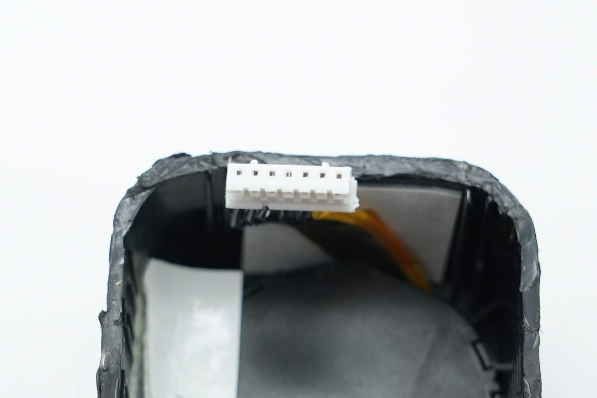
The retractable cable is connected to the PCBA module via a plug-in connection, and the inner side of the housing is lined with aerogel insulation cotton.
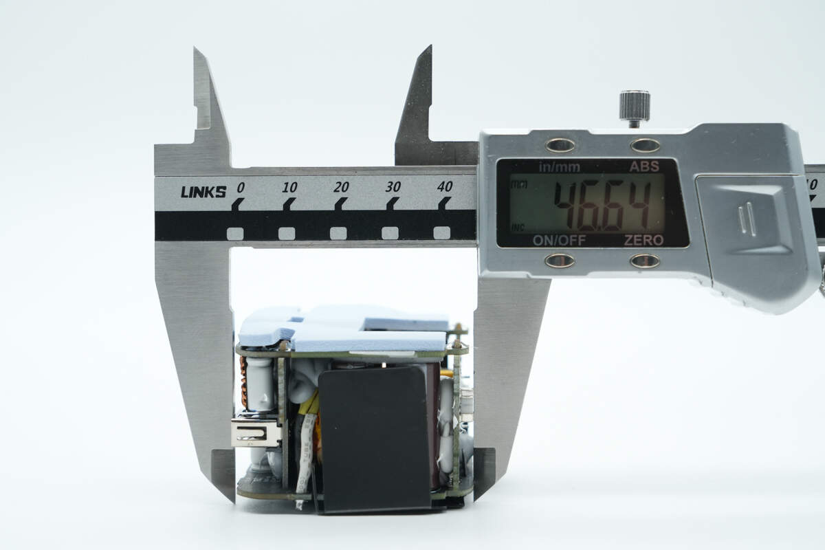
The length of the PCBA module is about 46.64 mm (1.84 inches).
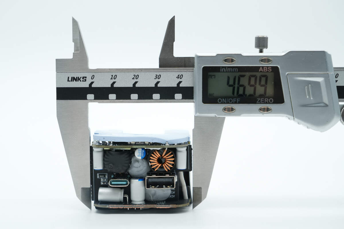
The width is about 46.99 mm (1.85 inches).
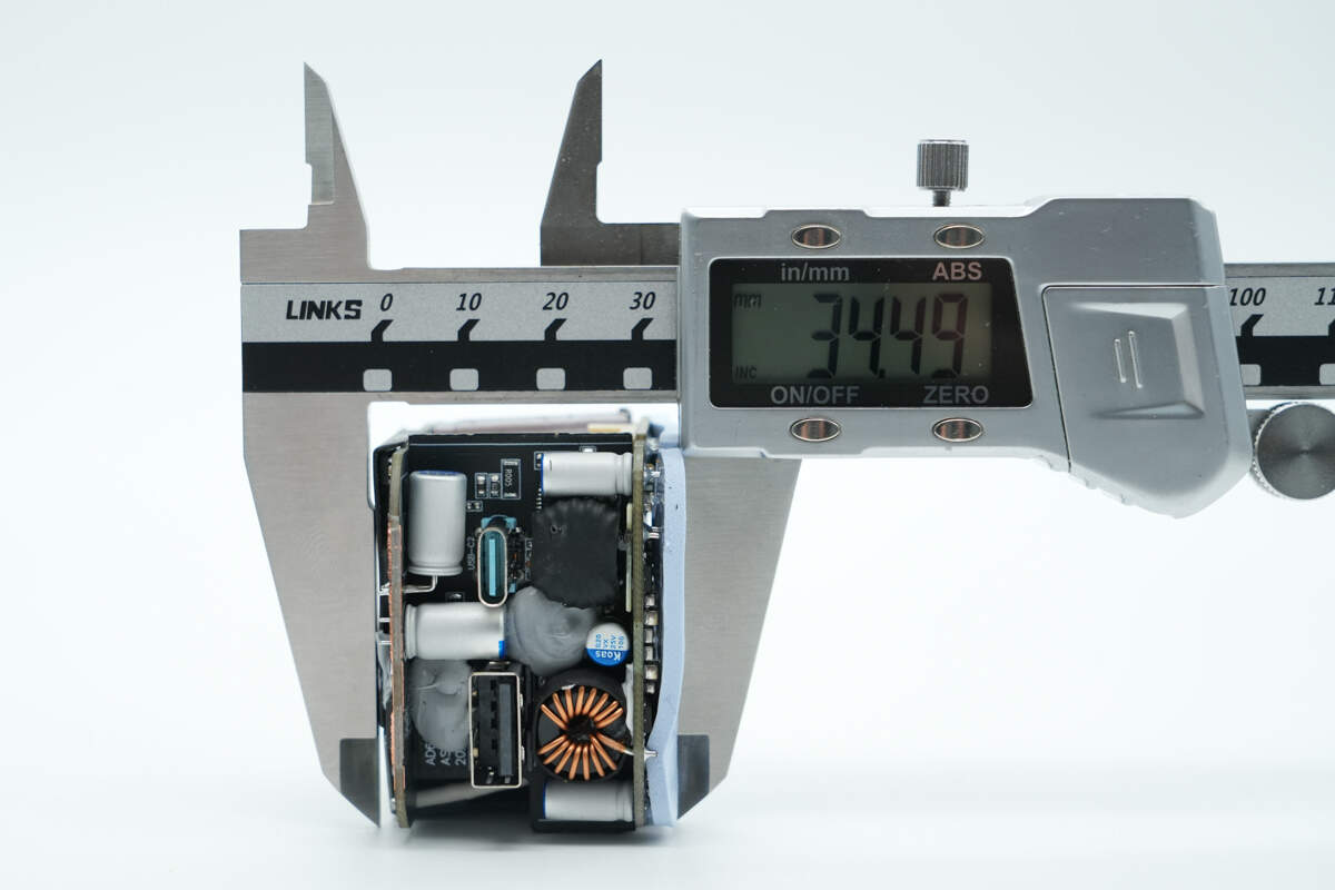
The thickness is about 34.49 mm (1.36 inches).
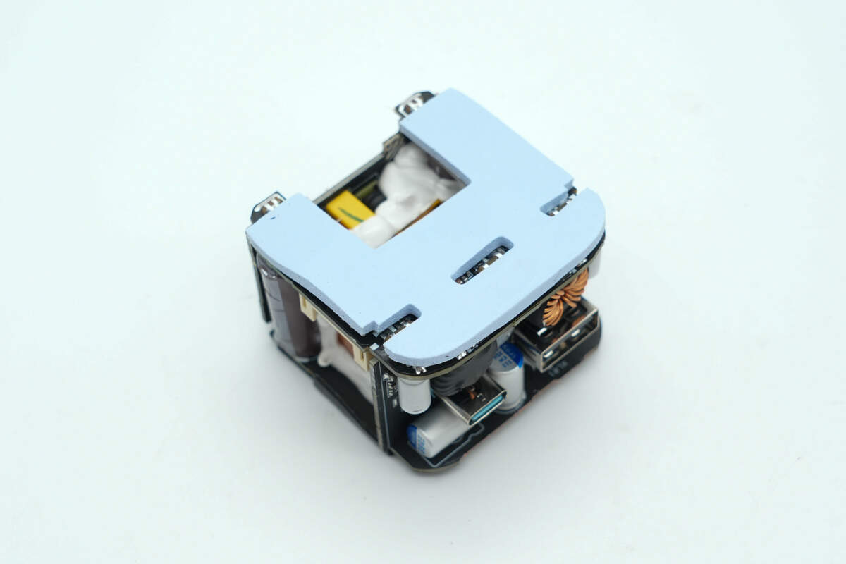
The PCBA module consists of four small PCBs, with a blue thermal pad covering the top. Components between the layers are reinforced with white adhesive.
The bottom and sides are covered with a one-piece Mylar sheet.
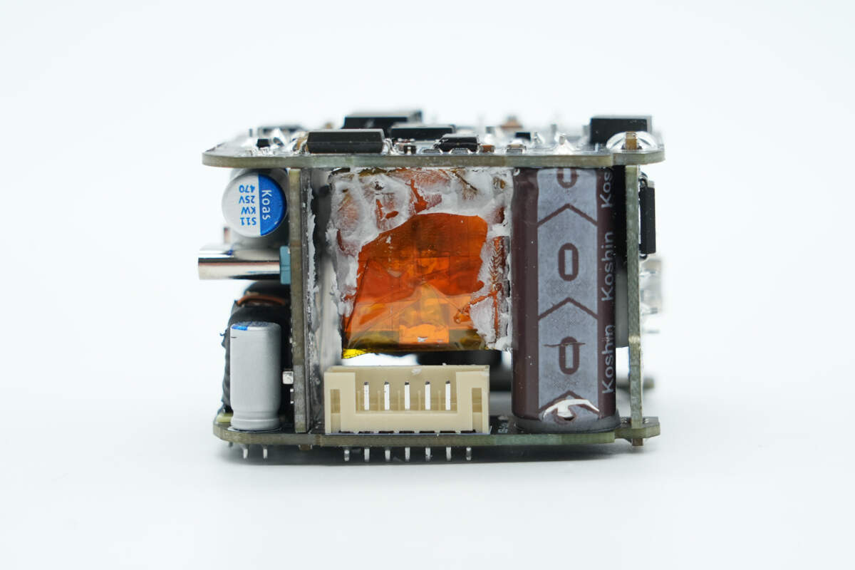
Components such as the transformer and capacitors are arranged within the space formed by the four small PCBs to maximize space utilization.
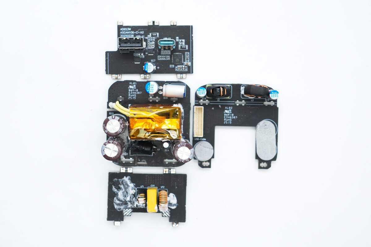
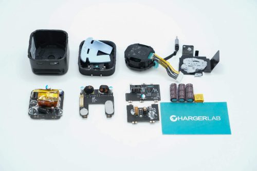
Separate the four small PCBs to facilitate understanding of the components on each PCB.
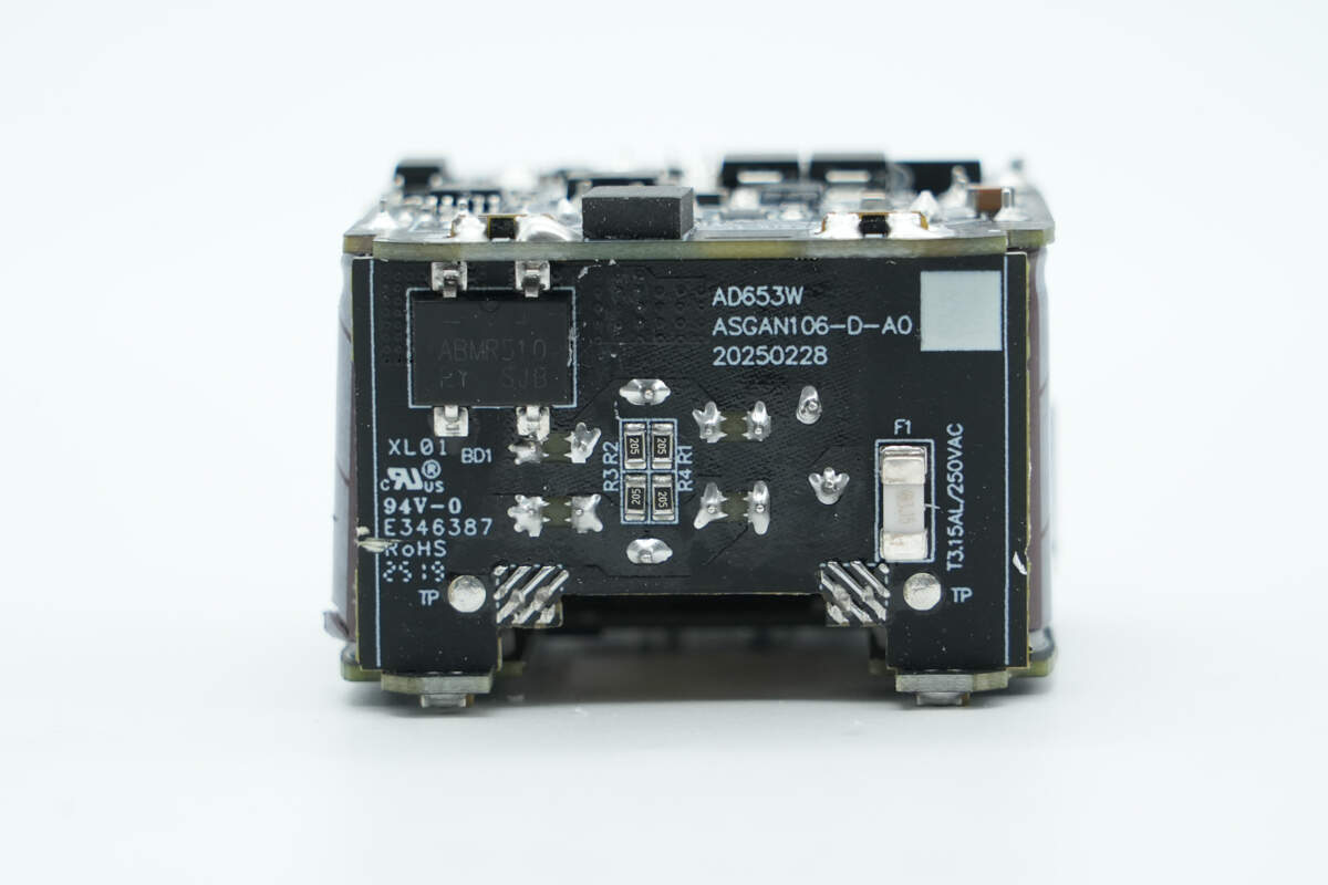
On the back side of the input-end PCB, there is an SMD fuse and a bridge rectifier.
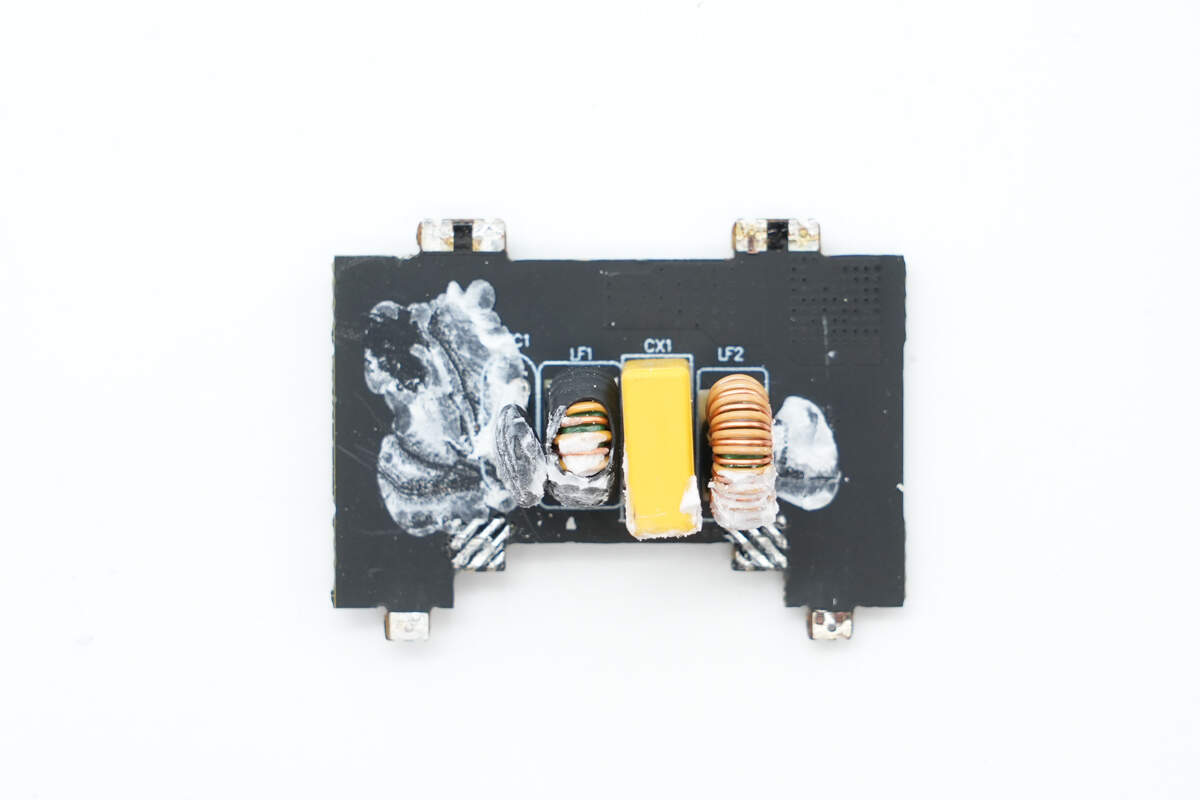
On the front side, there is an NTC thermistor, a safety X2 capacitor, and two common mode chokes.
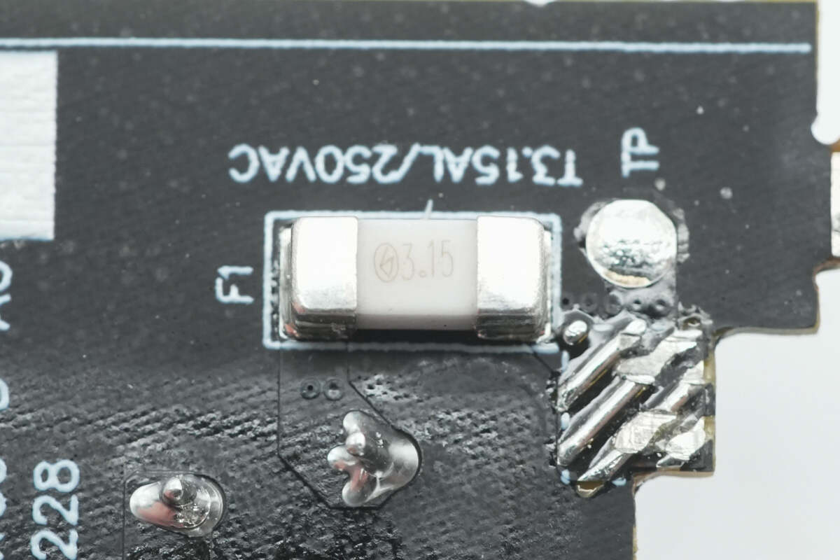
The SMD fuse is from Betterfuse with a rated current of 3.15A.
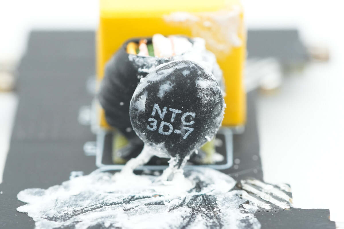
The NTC thermistor is used to suppress inrush current during power-up.
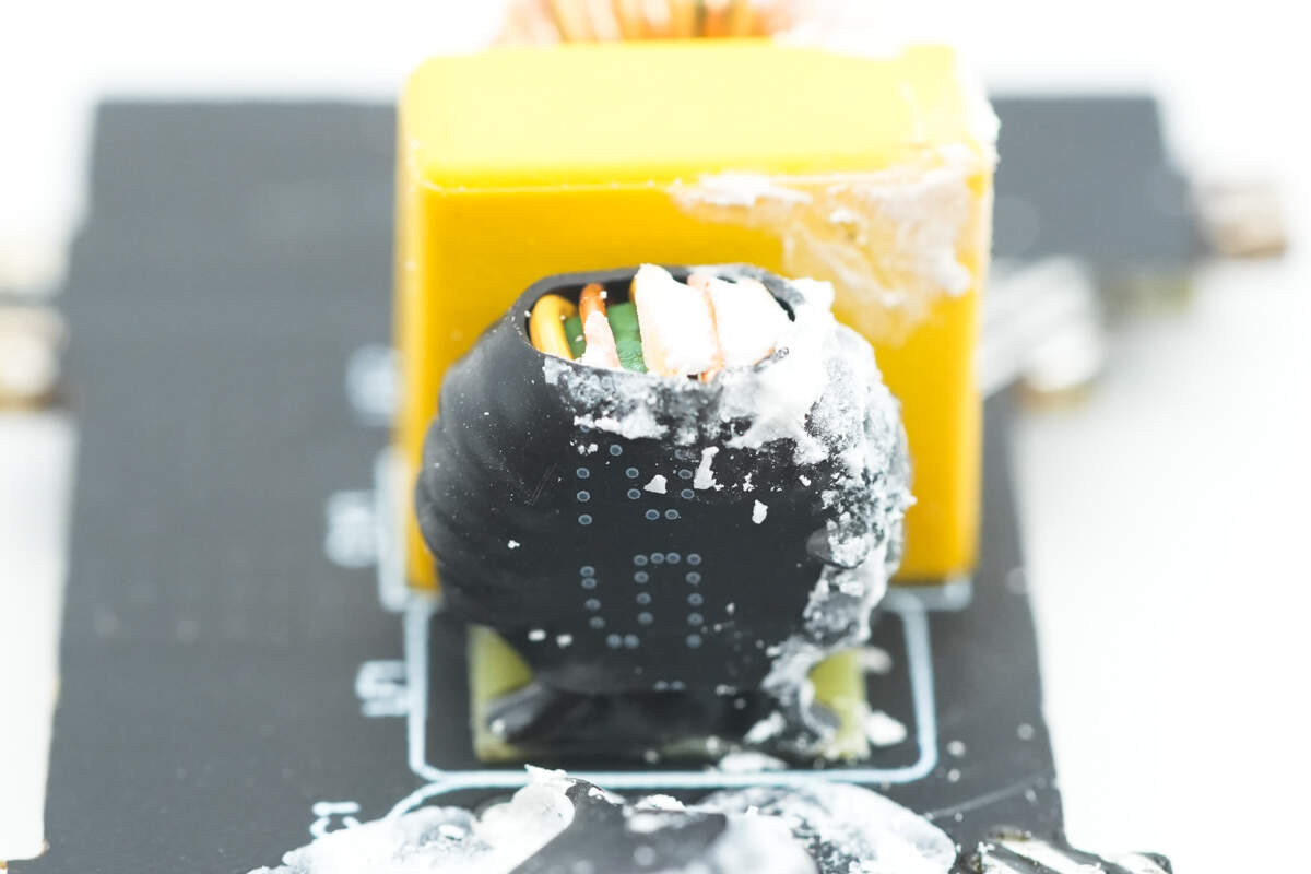
The common mode choke is wound with two wires and insulated with a heat shrink tube.
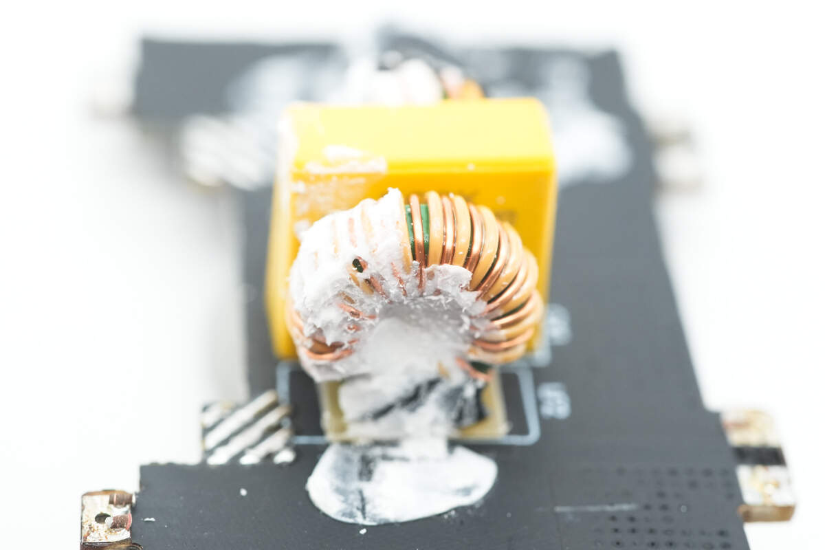
Close-up of the other common mode choke. The two-stage design provides better EMI interference filtering.
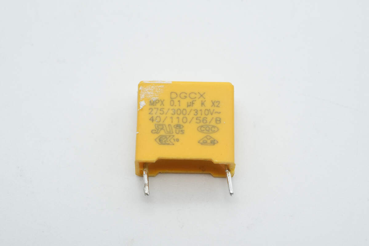
The safety X2 capacitor is from DGCX. 0.1μF.
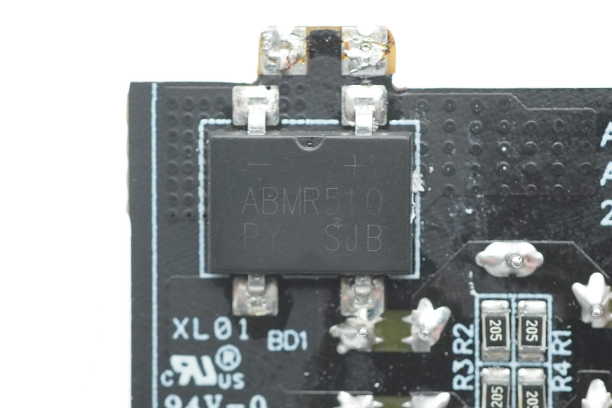
The bridge rectifier is from Pingwei, model ABMR510, rated at 5A 1000V, and uses an ABM package.
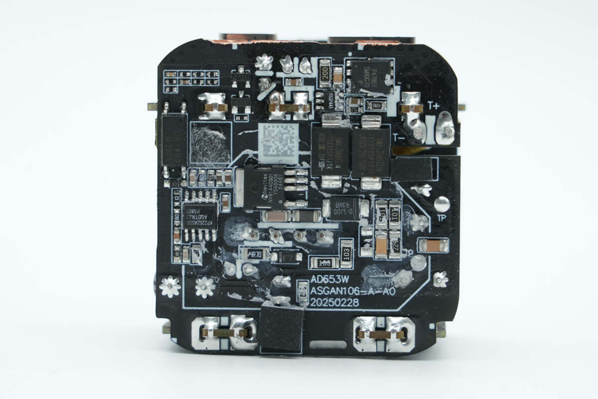
The back side of the bottom PCB houses the master control chip, primary MOSFET, synchronous rectifier, optocoupler, and SMD Y capacitors.
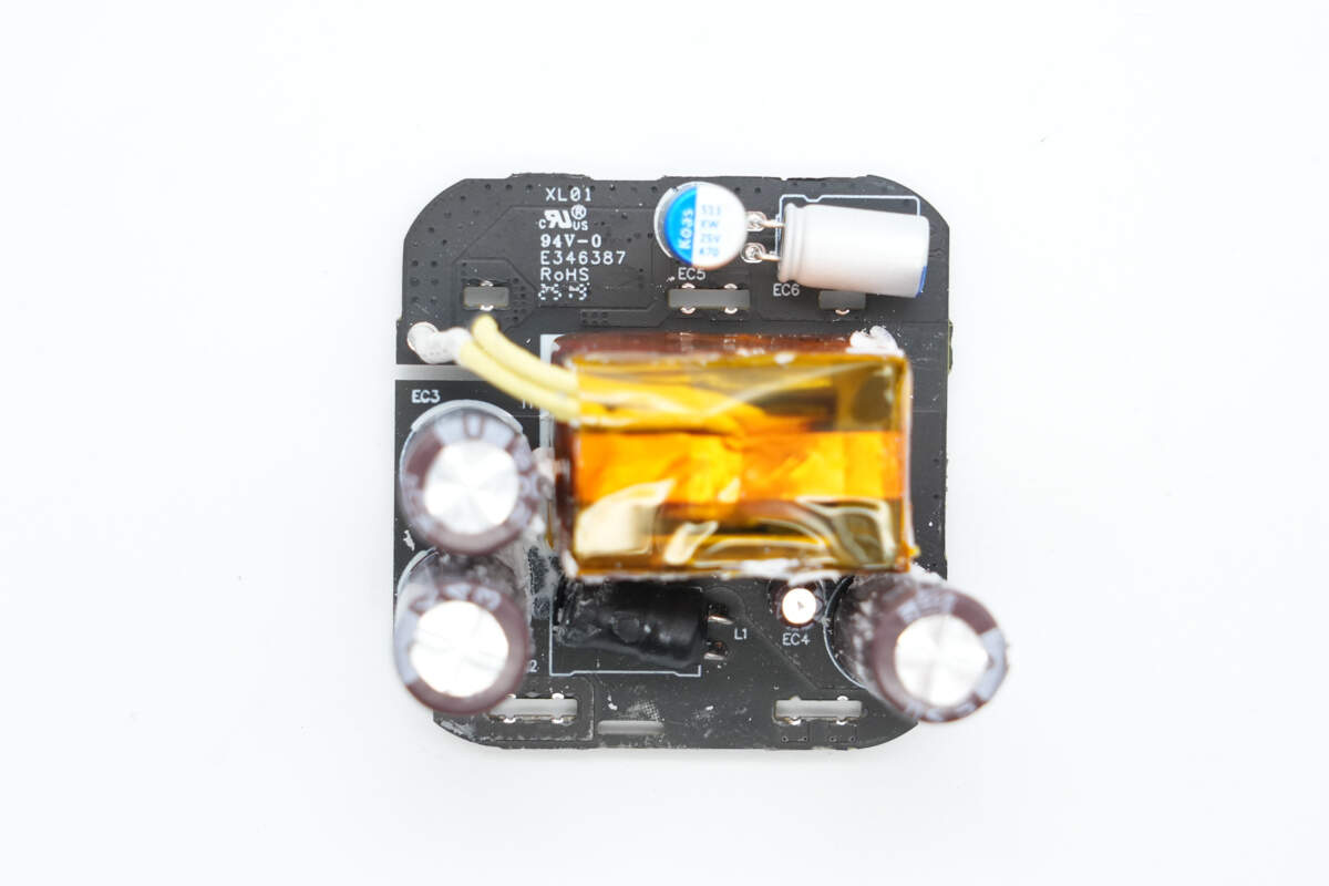
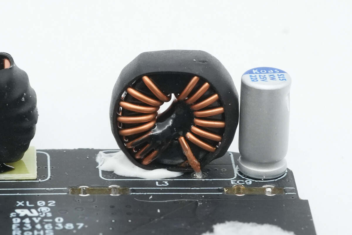
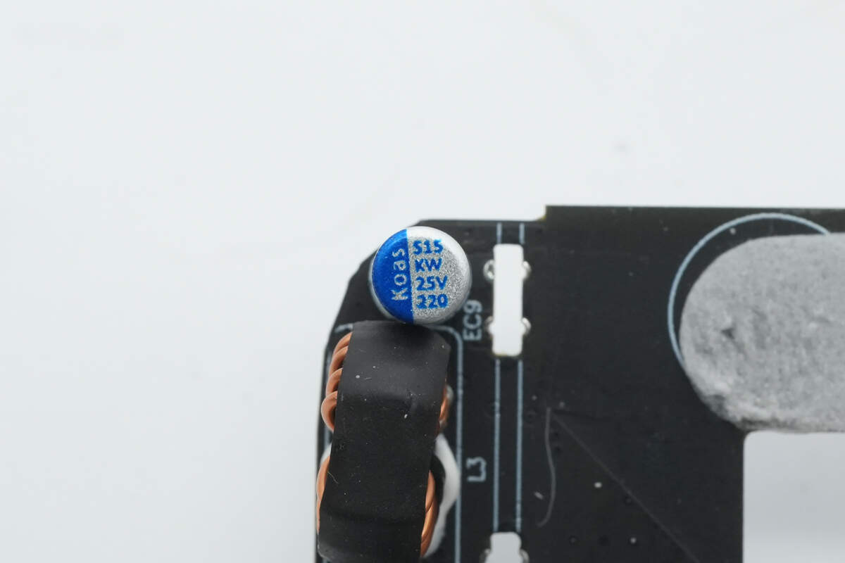
On the front side, there are capacitors, an I-shaped inductor, and a transformer.
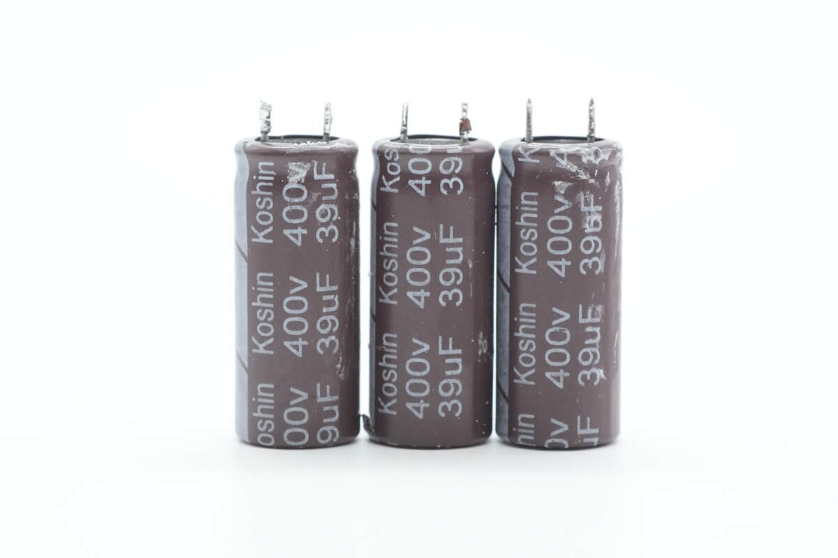
The three electrolytic capacitors are from Koshin, each rated at 400V 39μF.
The I-shaped inductor is insulated and protected with a heat shrink tube.
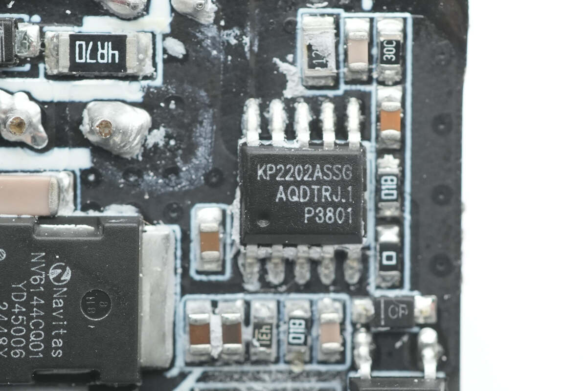
The switching power supply PWM controller uses the Kiwi Instruments KP2202. It features a built-in high-voltage startup function and integrates AC input brown-out detection and X-capacitor discharge functionality. The chip offers ±1% constant voltage accuracy, ultra-low startup and operating current, standby power consumption below 30 mW, and supports valley-lock operation mode.
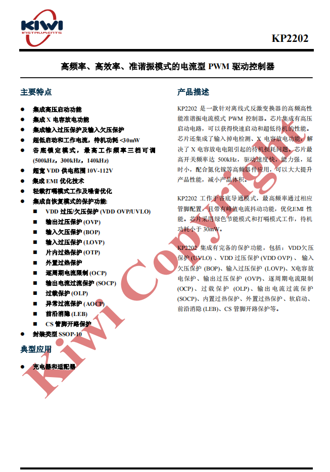
The KP2202 supports a maximum operating frequency adjustable in three levels: 500 kHz, 300 kHz, and 140 kHz. It implements frequency jitter through peak current modulation for improved EMI performance. The VDD supply voltage range is 10–112 V. The chip integrates comprehensive protection features and includes a built-in driver capable of driving CoolMOS and GaN FETs.
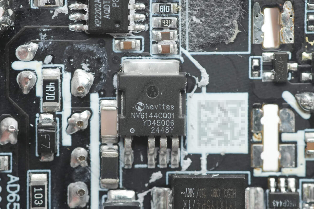
The primary MOSFET is from Navitas, model NV6144C, a GaNSlim gallium nitride power chip. It integrates a 700 V-rated, 260 mΩ high-performance enhancement-mode GaN FET, a gate driver, and extended features, all in a DPAK-4L package.
It's lossless current sensing technology eliminates the need for an external sense resistor, improving overall system efficiency. Built-in over-temperature protection enhances system robustness, while automatic standby and sleep modes optimize efficiency under light-load, ultra-light-load, and no-load conditions.
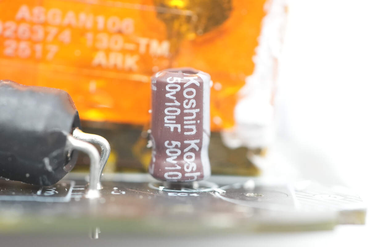
The capacitor that supplies power to the master control chip is also from Koshin, with a specification of 50V 10μF.
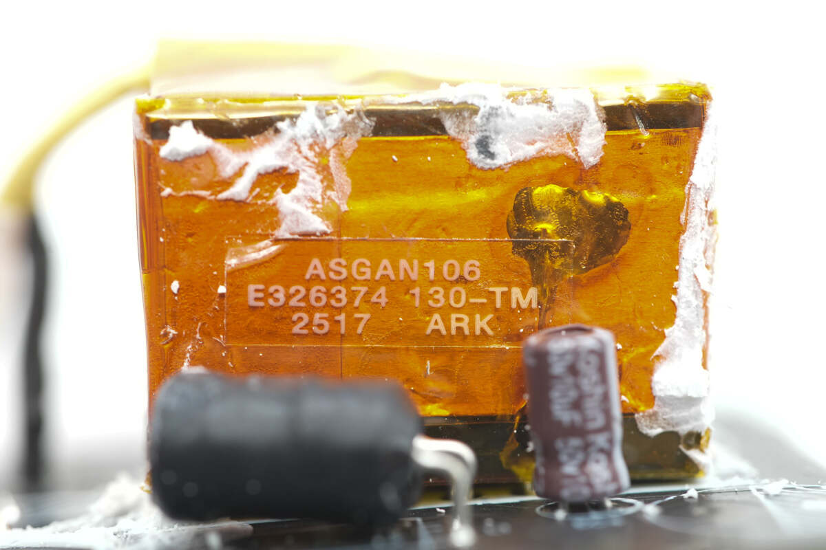
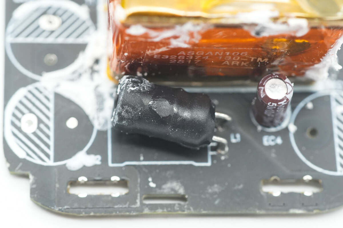
The transformer is wrapped with copper foil and high-temperature resistant insulating tape.
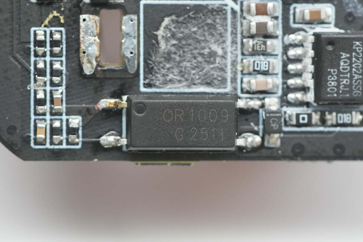
The OR1009 optocoupler is used for output voltage feedback.
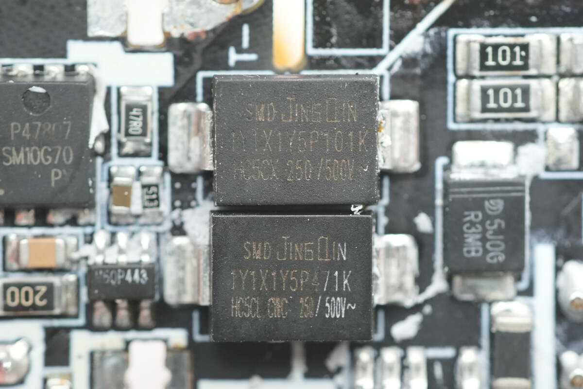
Two SMD Y capacitors are JinsQin SMD-1Y1X1Y5P471K, featuring a single-chip package with the code 2822 and dimensions of 7.0 × 5.6 × 2.4 mm. The package has bent leads inside, providing a safer creepage distance. Their capacitance ranges from 10 pF to 2200 pF, with a rated voltage of 500 V. These capacitors offer high integration and low cost, making them easy to apply in various electronic devices to enhance performance and reliability.
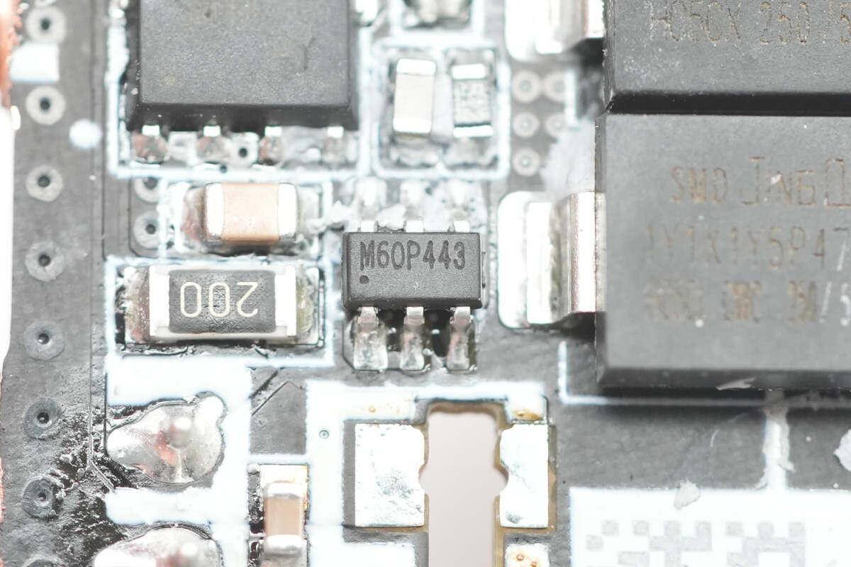
The synchronous rectifier controller marked with M6 is from Kiwi Instruments, model KP4060. It supports DCM, CCM, and QR operating modes as well as active clamp Flyback topology. The controller operates at up to 600 kHz and integrates high-voltage detection and high-voltage power supply circuits. It features intelligent dual LDOs, eliminating the need for an auxiliary winding power supply, and supports synchronous rectifier operation during output short circuits. The device comes in a space-saving SOT23-6 package.
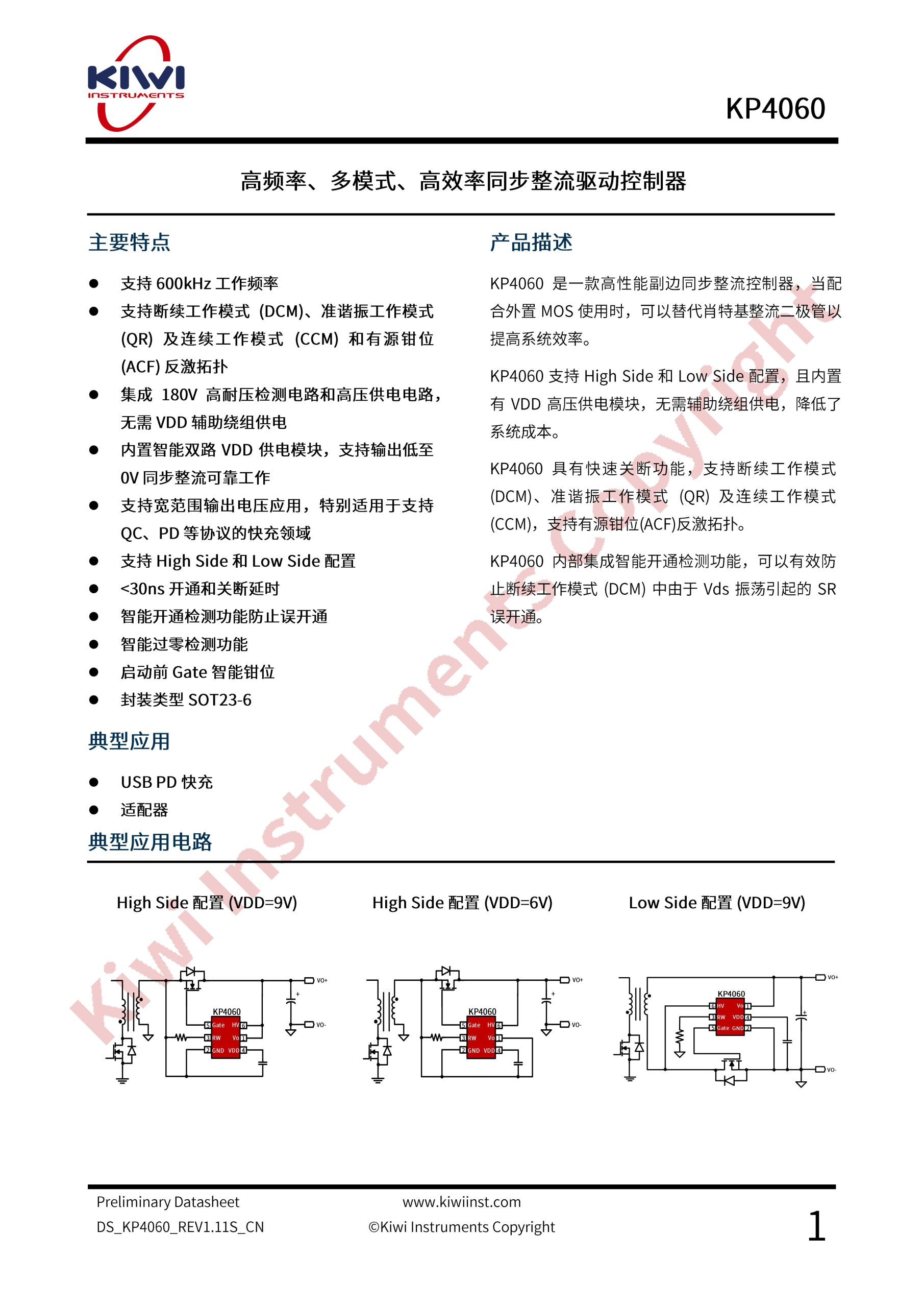
The KP4060 supports a wide range of output voltage applications and is especially suitable for fast-charging fields supporting protocols such as QC and PD. It supports both high-side and low-side configurations. With less than 30 ns turn-on and turn-off delay, its gate driver clamp technology prevents false triggering caused by parasitic coupling. It also features patented intelligent current zero-cross turn-off and smart turn-on detection technologies to prevent false switching, ensuring safe operation.
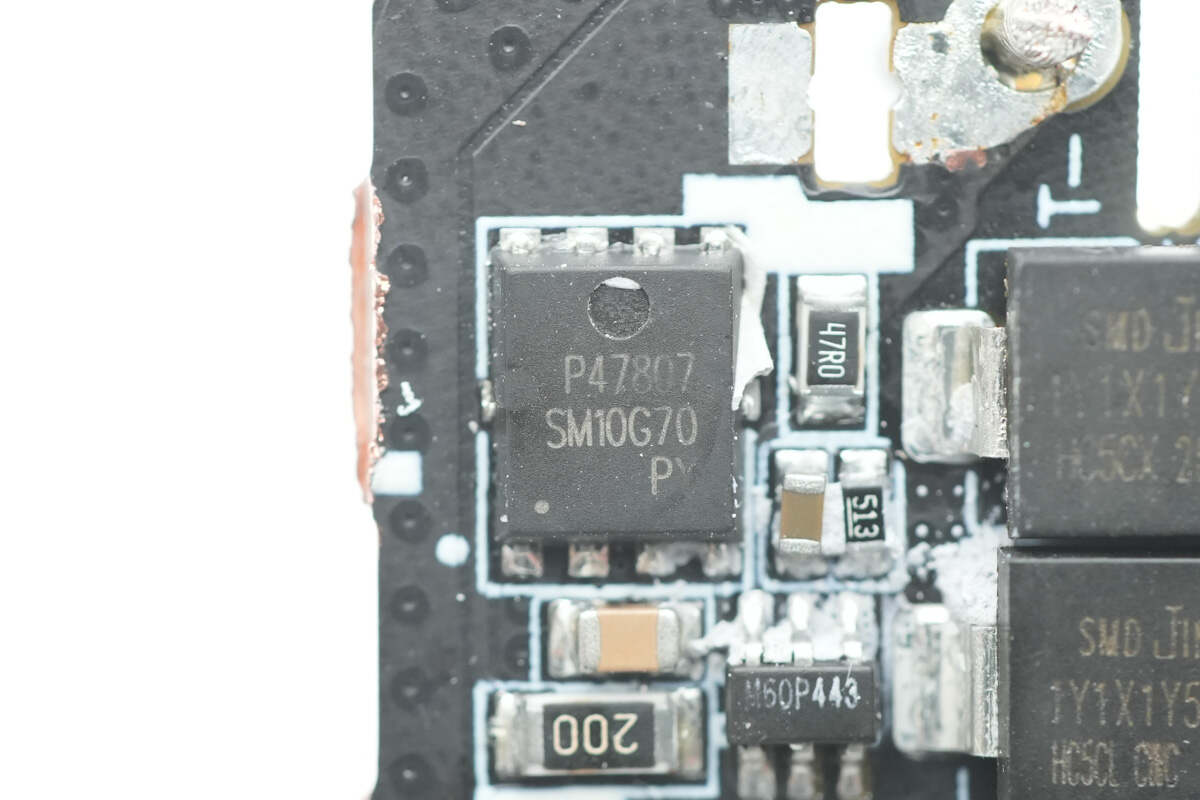
The synchronous rectifier marked with SM10G70 uses a DFN 5×6 package.
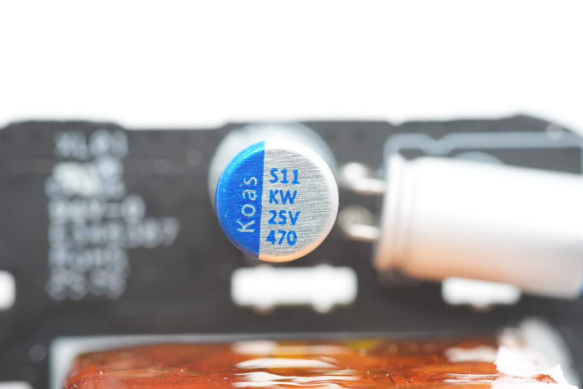
The solid capacitor is from Koshin, with a specification of 25V 470μF.
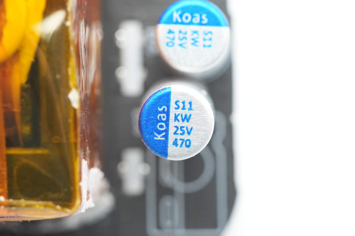
The other capacitor has the same part number.
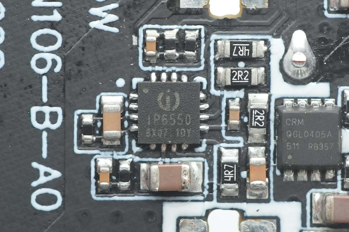
On the back side of the top PCB, there are two synchronous buck controllers for secondary step-down circuits, synchronous buck MOSFETs, the protocol chip for the USB-C cable, and the VBUS MOSFET.
On the other side, there are buck inductors and solid capacitors paired with the two secondary step-down circuits.
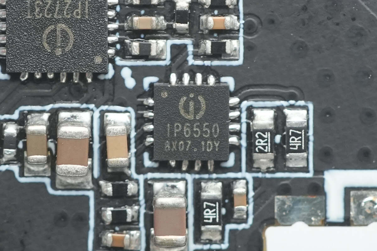
The synchronous buck controller for the USB-C cable’s secondary step-down circuit is the Injoinic IP6550. It supports a 36V input, features a built-in NMOS driver, and uses two external MOSFETs for efficient synchronous rectification and step-down conversion. The output voltage is regulated via a feedback pin. It operates at a switching frequency of 135 kHz, with an input voltage tolerance up to 48V, and includes comprehensive protection features. The device comes in a compact 3×3 mm QFN16 package, enabling simplified synchronous buck converter designs.
The IP6550 is suitable for applications such as automotive chargers, multi-port adapters, smart power strips, USB-C interface power strips, and dashcams. Its synchronous rectification provides high conversion efficiency and supports high output currents for multi-port 5V outputs. When paired with a PD protocol chip, it enables wide-range voltage adjustment to meet USB PD 3.1 standards.
Here is the information about Injoinic IP6550.
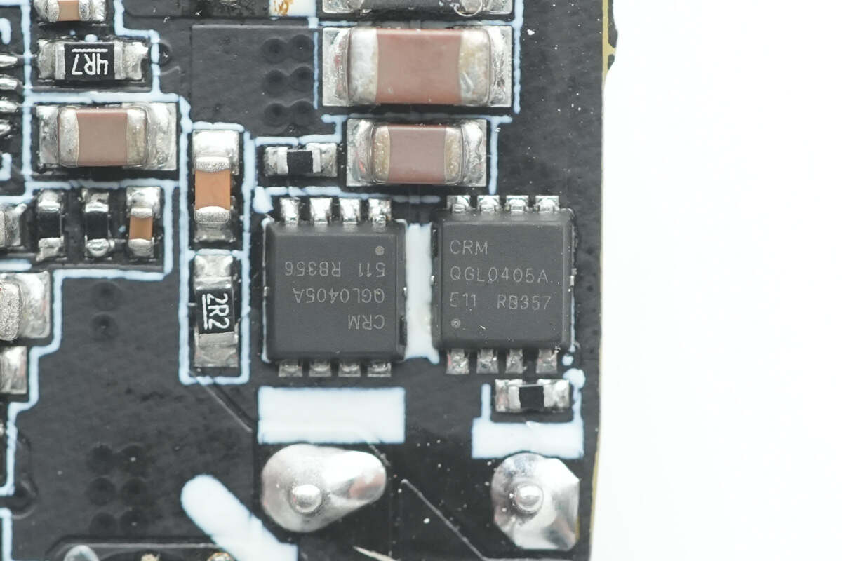
The paired synchronous buck MOSFETs are from CRM, model CRMQGL0405A. They are NMOS devices with a 40V rating and come in a PDFN 3.3 × 3.3 mm 8L package.
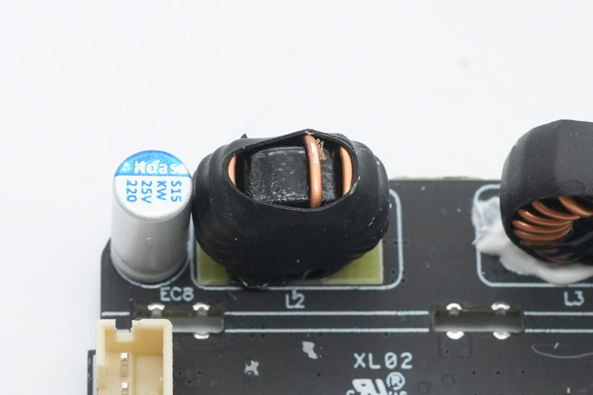
The paired buck inductors are insulated and protected with heat shrink tubing and have a bakelite base on the bottom.
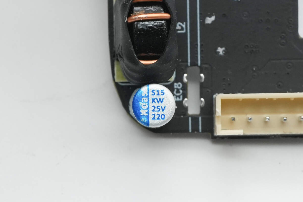
The secondary buck solid capacitor is from Koshin, rated at 25V 220μF.
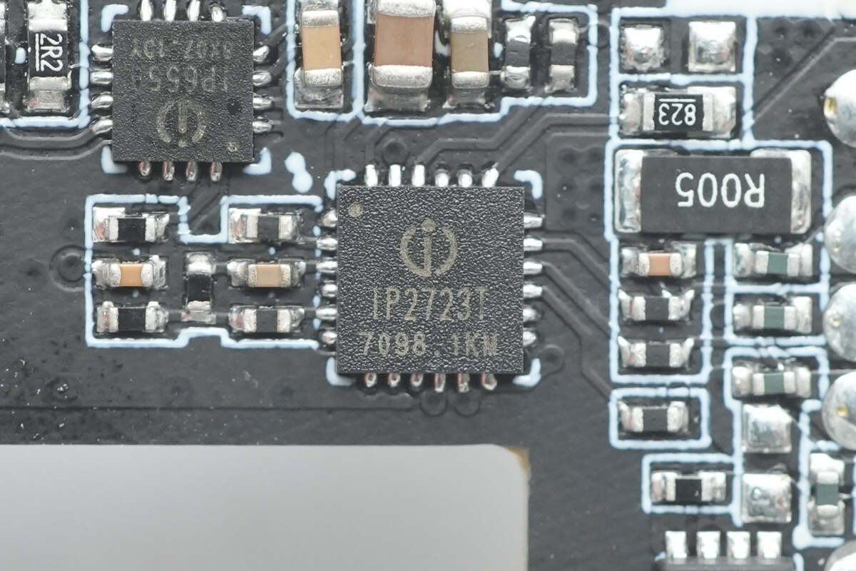
The USB-C cable’s protocol chip is the Injoinic IP2723T, certified by the USB-IF association for PD 3.0 PPS, with TID: 3135. It is a multi-protocol integrated IC designed for USB output ports. It supports a wide range of fast-charging protocols, including USB Type-C DFP, PD 2.0/3.0, PPS, HVDCP QC4, QC4+, QC3.0/2.0, FCP, SCP, AFC, MTK PE+ 2.0/1.1, Apple 2.4A, BC1.2, and Samsung 2.0A.
This chip provides a complete Type-C solution for unidirectional output applications such as adapters and car chargers. It features high integration and rich functionality, requiring minimal external components, effectively reducing the overall solution size and lowering BOM cost.
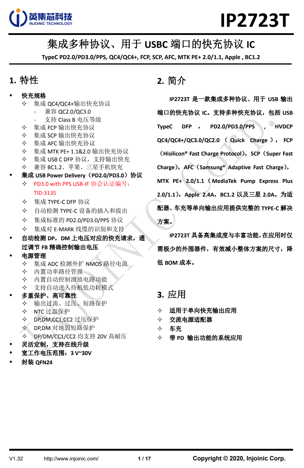
Here is the information about Injoinic IP2723T.
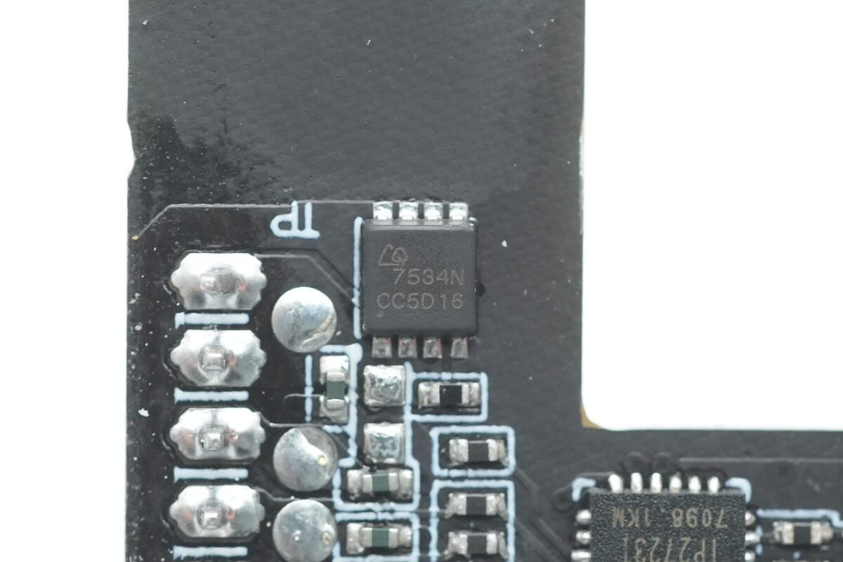
The VBUS MOSFET is the CQAOS CQY7534N, an NMOS device rated for 30V with an on-resistance of 4.8 mΩ. It comes in a DFN3×3EP package.
The other secondary buck circuit uses the same design, with the synchronous buck controller also being the Injoinic IP6550.
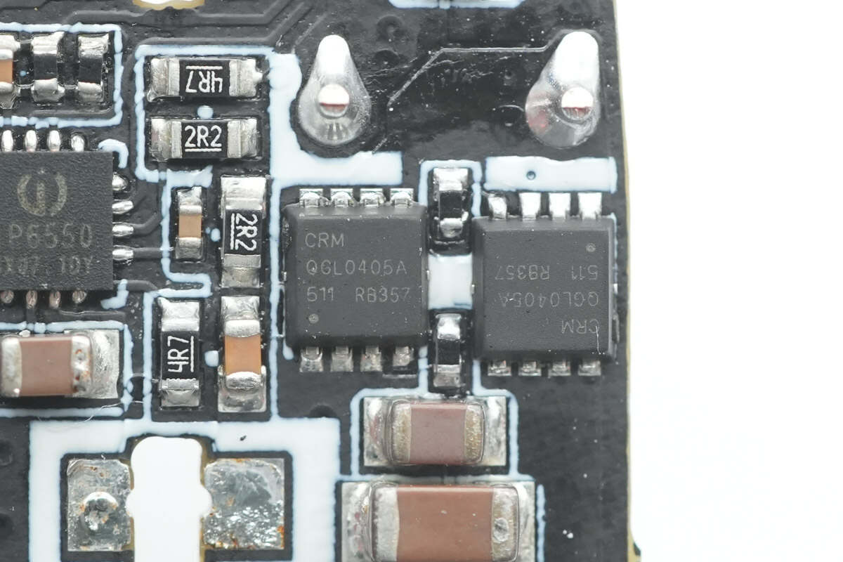
The two synchronous buck MOSFETs used in this circuit are also CRM CRMQGL0405A.
The buck inductor is insulated with heat shrink tubing.
The solid capacitor is also from Koshin. 25V 220μF.

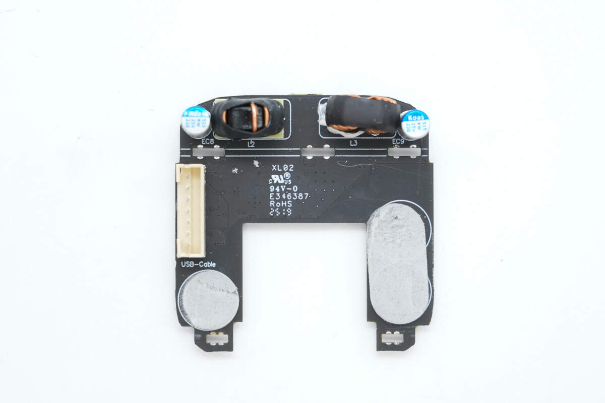
Two USB sockets are soldered onto the output-end PCB.
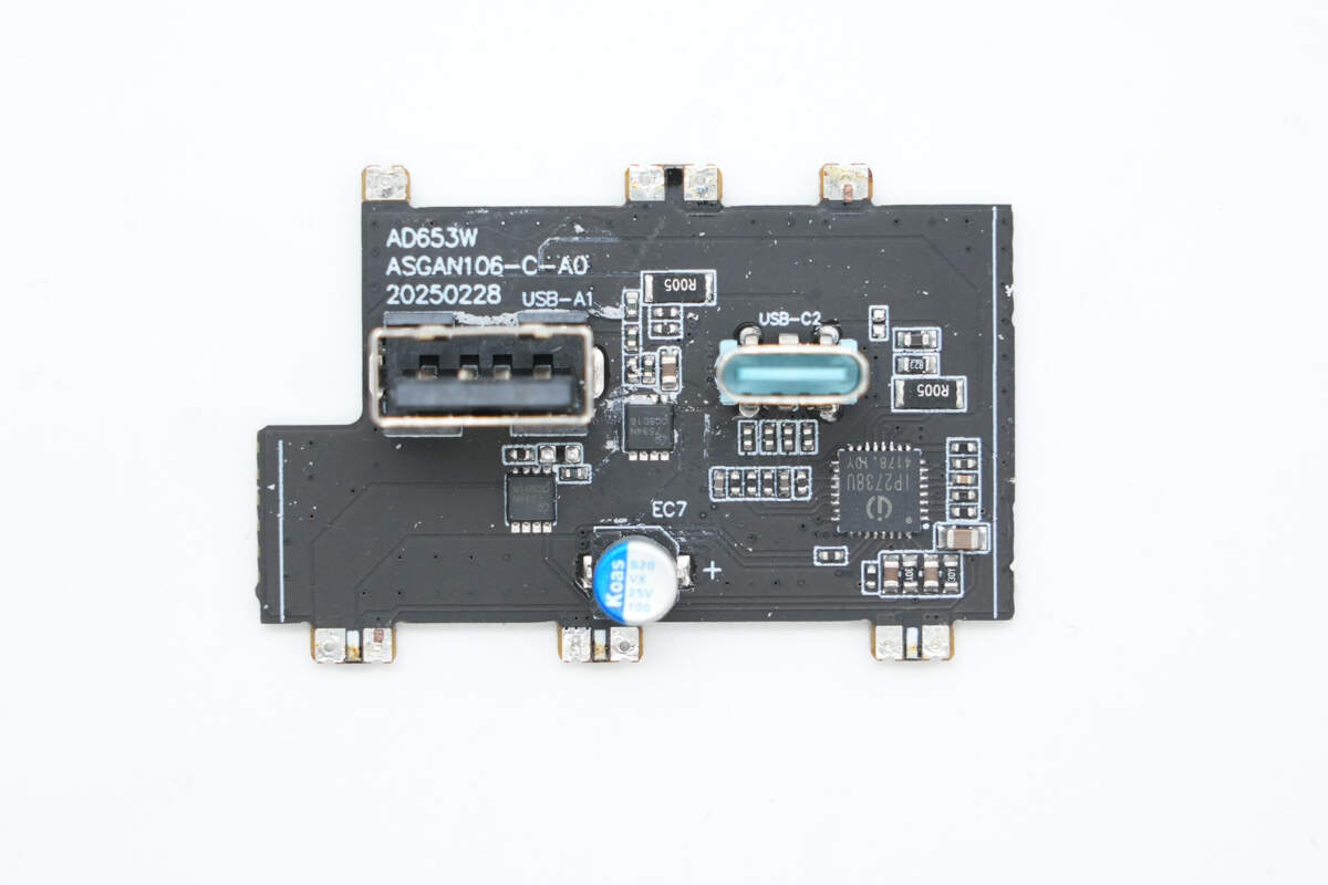
The front side of the PCB also features a solid capacitor for output filtering, a protocol chip, and a VBUS MOSFET.
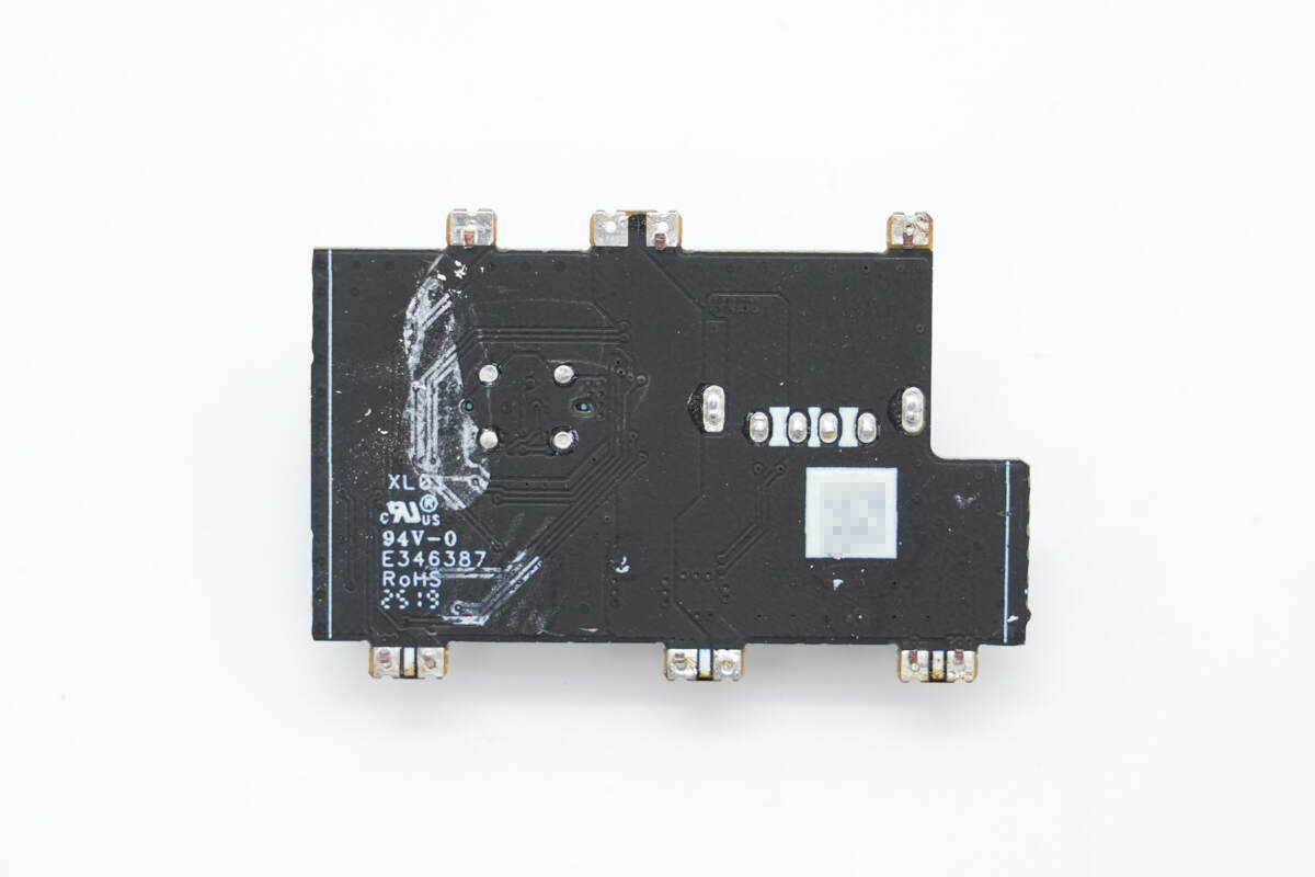
There are no components on the back.
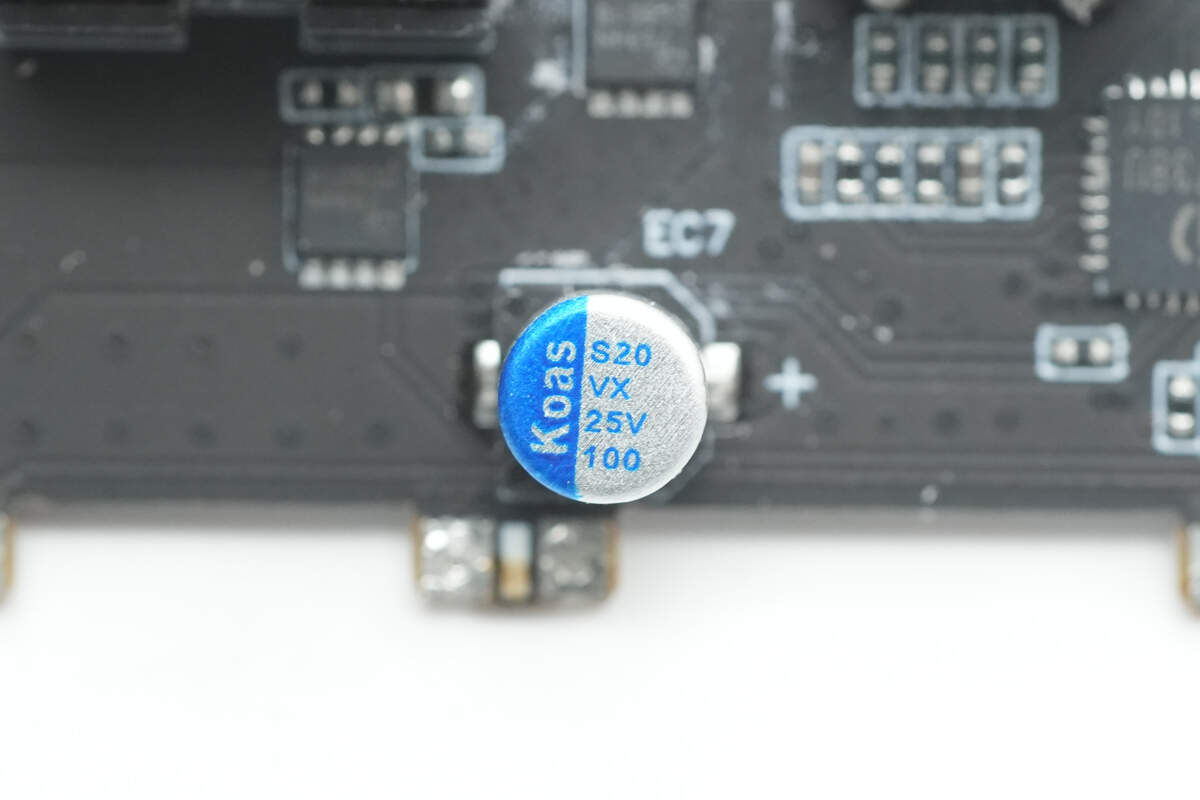
The other solid capacitor is also from Koshin. 25V 100μF.
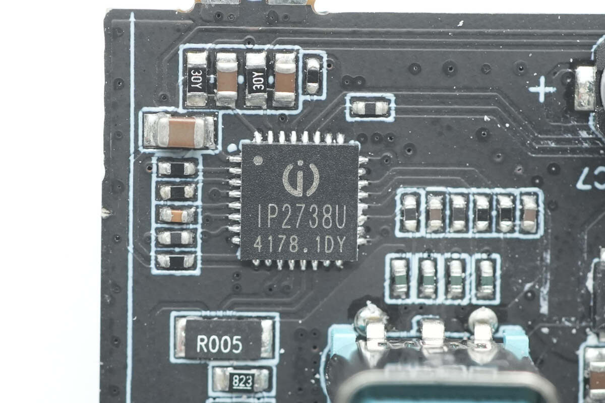
The protocol chip for USB-C2 and USB-A ports is the Injoinic IP2738U. It supports multiple USB interfaces and dual-port fast charging applications ranging from 18W to 140W. The chip features independent feedback control and USB PD control, effectively integrating two IP2736 chips into one. Its fast-charging specifications are identical to the IP2736. The IP2738U supports USB PD 3.1 with 28V EPR levels, as well as a wide range of fast-charging protocols including PD 3.0 and PPS, ensuring excellent compatibility.
Internally, the Injoinic IP2738U includes four independent NMOS drivers to control multiple output interfaces, manage multiple VBUS MOSFETs for output port switching, and enable dual power source parallel control. It also supports independent dual-channel overcurrent, overvoltage, and short-circuit protection, ensuring safe operation.
Here is the information about Injoinic IP2738U.
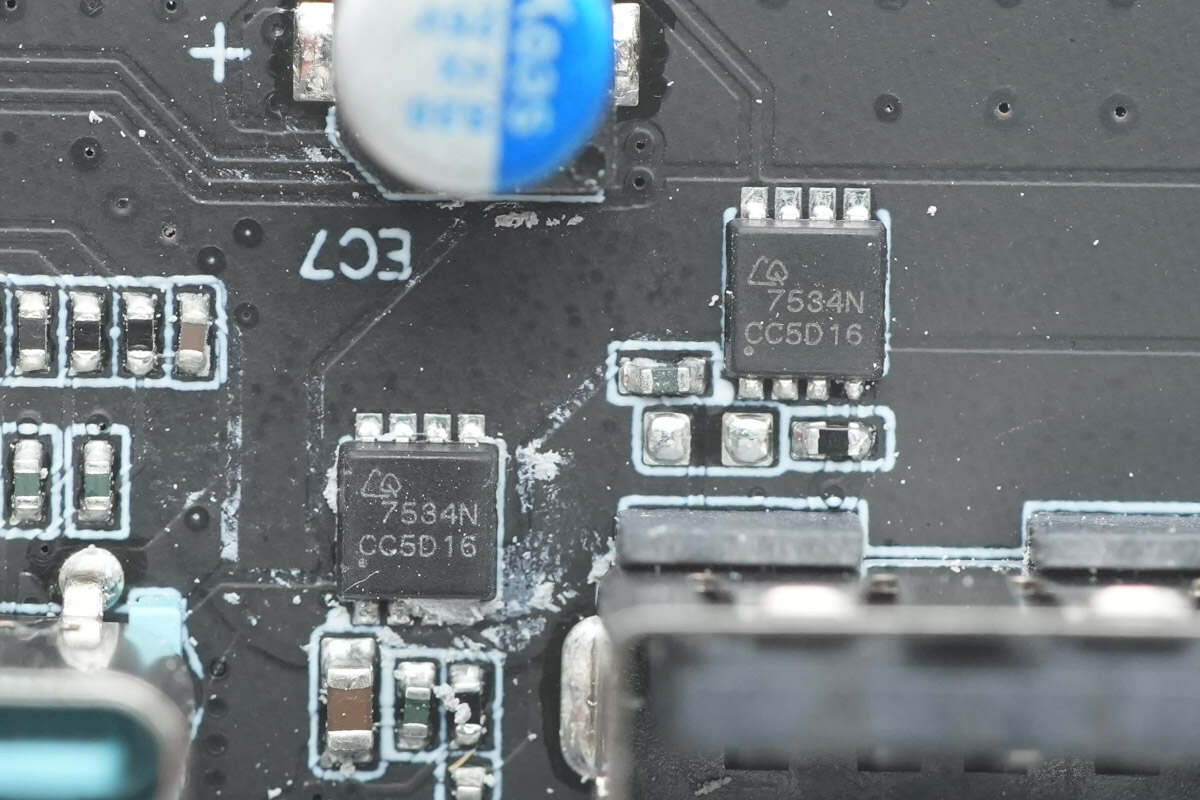
Both USB ports’ VBUS MOSFETs use the CQAOS CQY7534N.
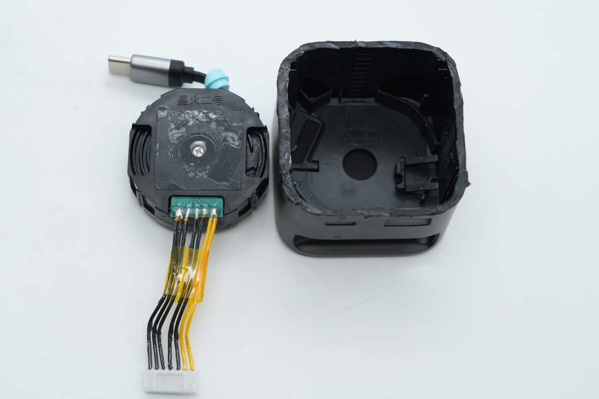
Remove the retractable cable module.
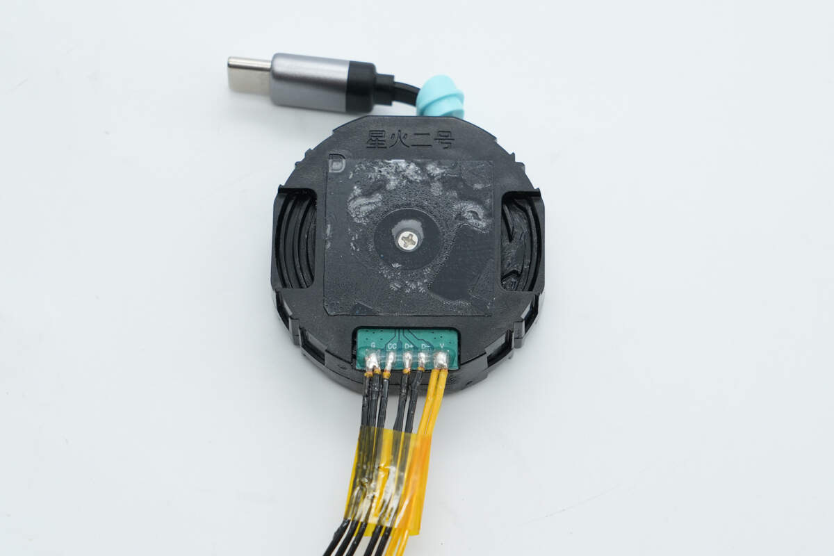
The module housing is secured with snap fits and screws.
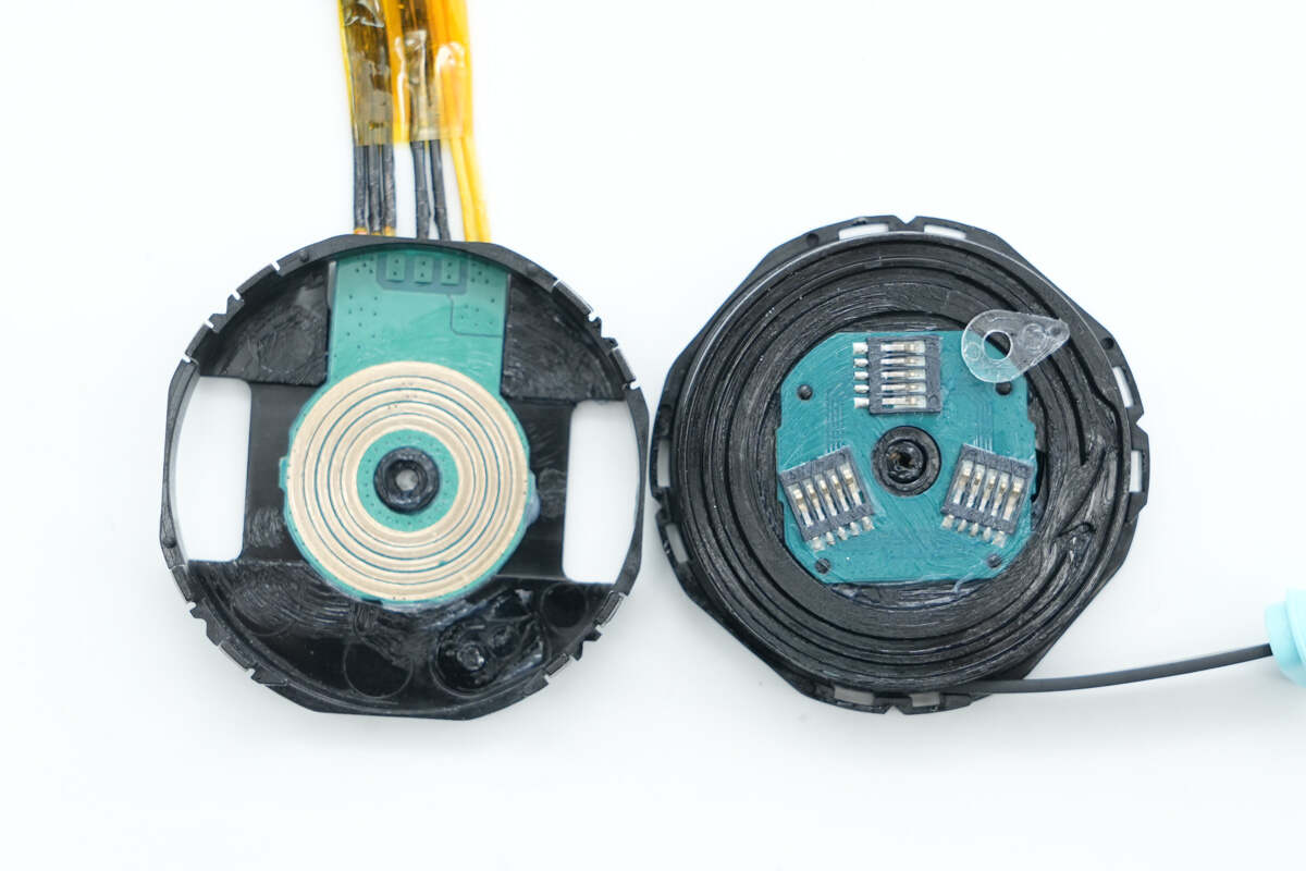
Here’s a look inside the module after disassembly.

Well, those are all components of the CUKTECH 67W CP6 GaN Charger.
Summary of ChargerLAB
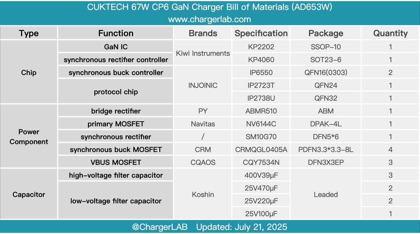
Here is the component list of the CUKTECH 67W CP6 GaN Charger for your convenience.
The case is made of V0-grade high-temperature-resistant material, offering a higher safety level. The weight is only 165g. The retractable USB-C cable has passed over 10,000 bending tests and more than 20,000 rapid retraction tests, ensuring durability and long service life. It supports 65W PD charging as well as Xiaomi's 67W proprietary protocol, and allows a 45W + 20W dual-output power strategy.
After taking it apart, we found it is designed based on the Kiwi Instruments KP2202 + KP4060 solution and uses the Navitas NV6144C GaN FET. It features two secondary buck circuits, both utilizing Injoinic IP6550 synchronous buck controllers. The protocol chips IP2723T and IP2738U are used to control the retractable cable and USB ports outputs, respectively. The module consists of four small PCBs with a thermal pad on top to aid heat dissipation. Components such as capacitors and the transformer are reinforced with adhesive for added mechanical stability.
Related Articles:
1. Teardown of Bitmain 1600W Power Supply (APW3++-12-1600-A3)
2. Teardown of Newsmy P72 100W 72000mAh Portable Power Station
3. Teardown of HONOR 100W USB-C GaN Charger