Introduction
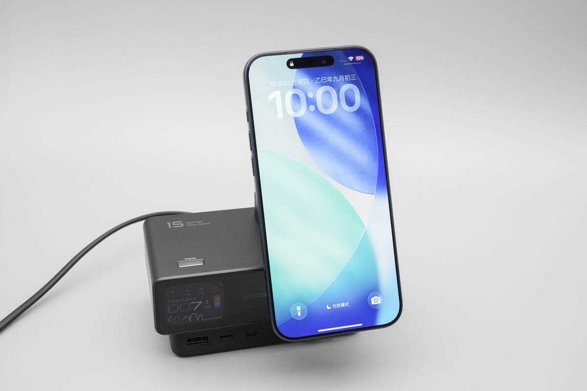
CUKTECH has released the new CUKTECH 15 Charging Station, a versatile power solution integrating wireless charging and a retractable cable. It can charge multiple devices simultaneously, including smartphones, earbuds, and laptops. The unit includes a built-in USB-C cable, two USB-C ports, and one USB-A port, along with magnetic and standard wireless charging functions.
It supports PD3.1 140W fast charging, Xiaomi’s 120W proprietary protocol, and ADC2.0 adaptive fast charging, ensuring broad compatibility across different brands. The magnetic wireless charging system can charge an iPhone and AirPods at the same time. The built-in cable extends to about 70 cm.
A 1.83-inch TFT display shows real-time output power for each port, and an internal NTC sensor provides thermal protection to ensure safe operation. Let’s take a closer look at its internal components and design.
Product Appearance
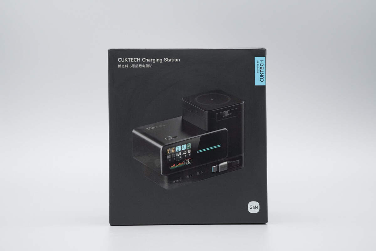
The front of the packaging box features the product name, appearance image, the “GaN” mark, and the phrase “Powered by CUKTECH.”
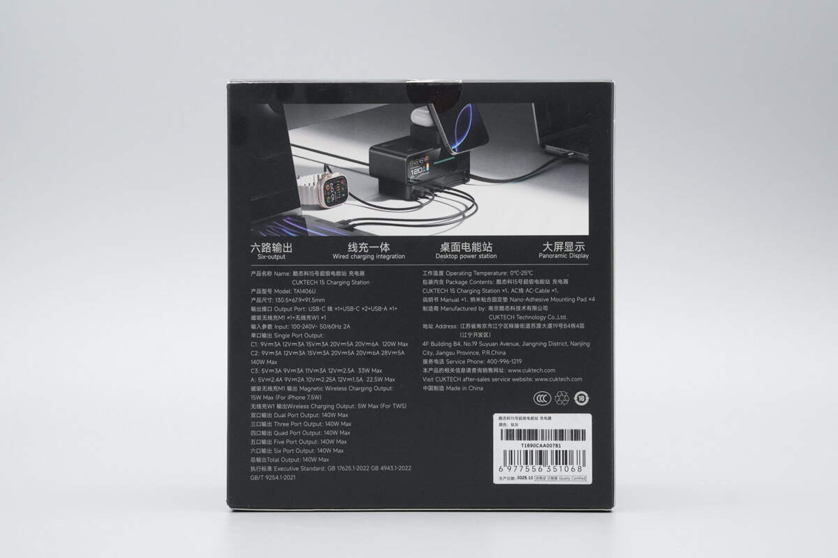
The back of the packaging displays the product’s usage scenarios and technical specifications.

The package includes the CUKTECH 15 Charging Station, a power cord, and a user manual.
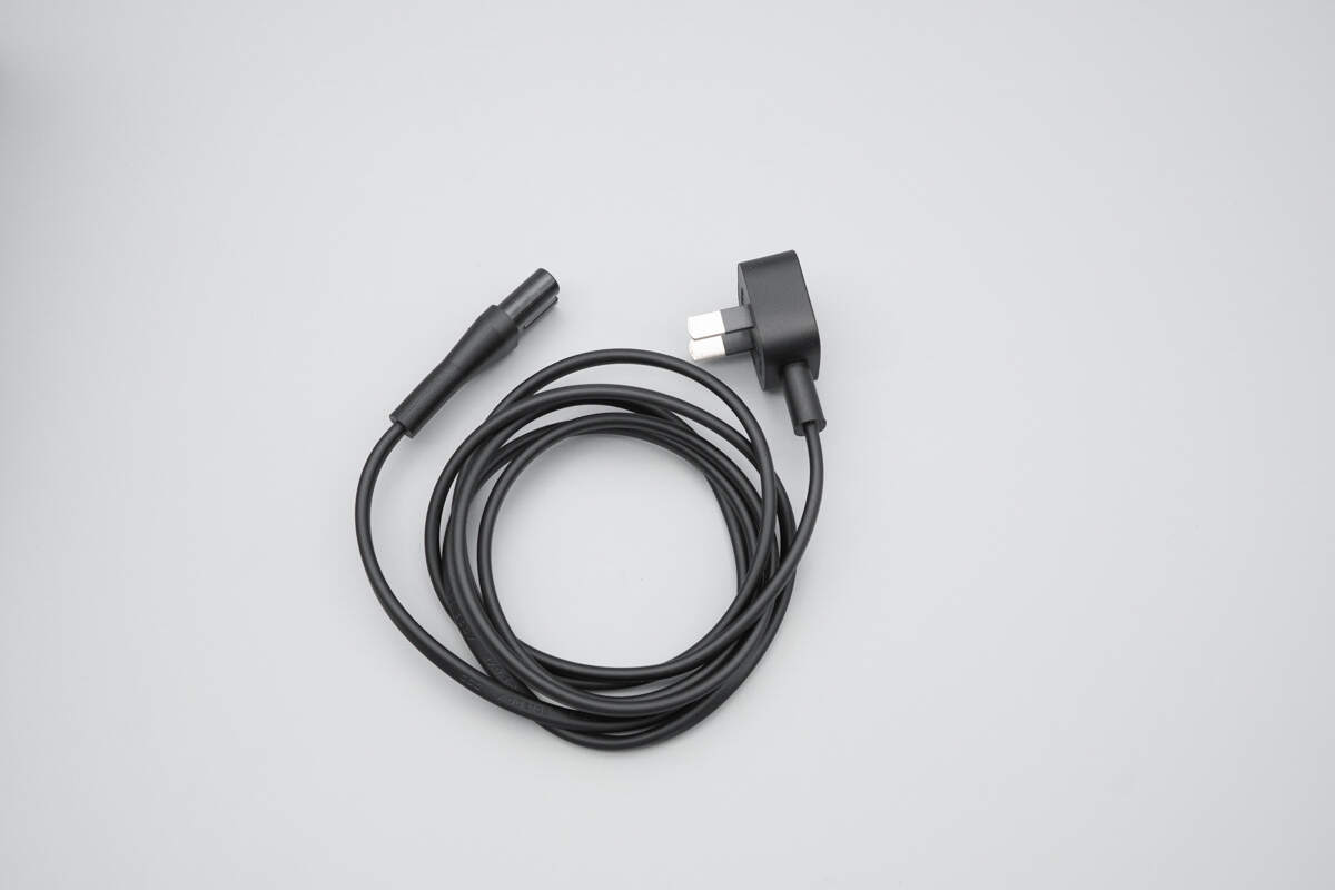
The power cord is black.
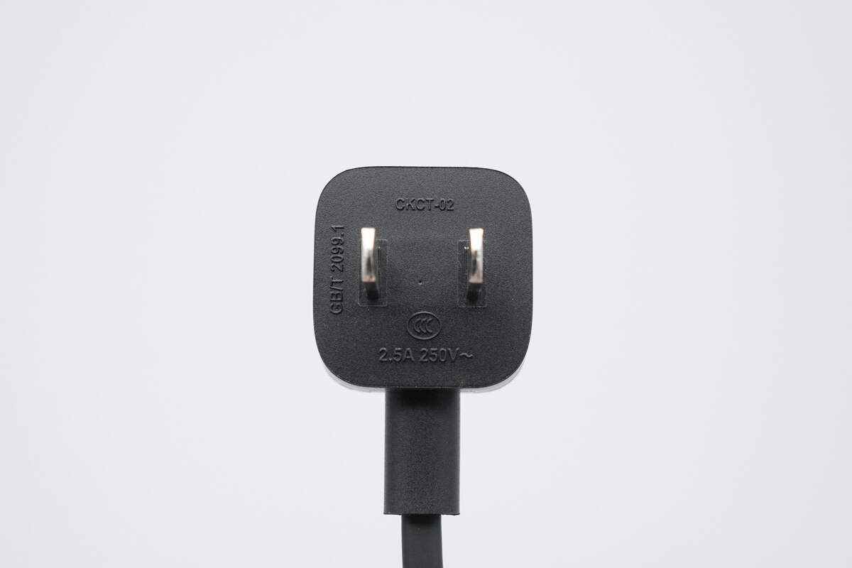
The plug is rated at 2.5A, 250V~, and has passed CCC certification.
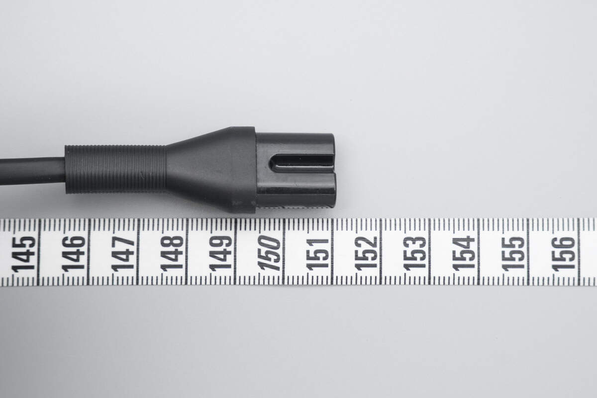
The length of the power cord is about 1.5 m.
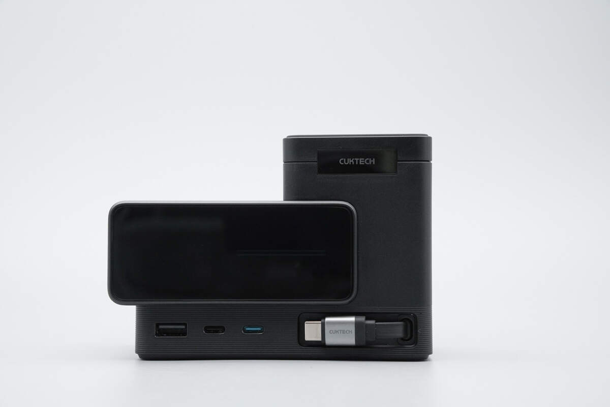
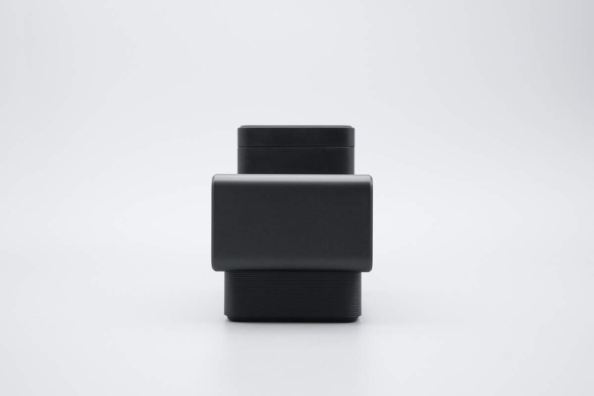
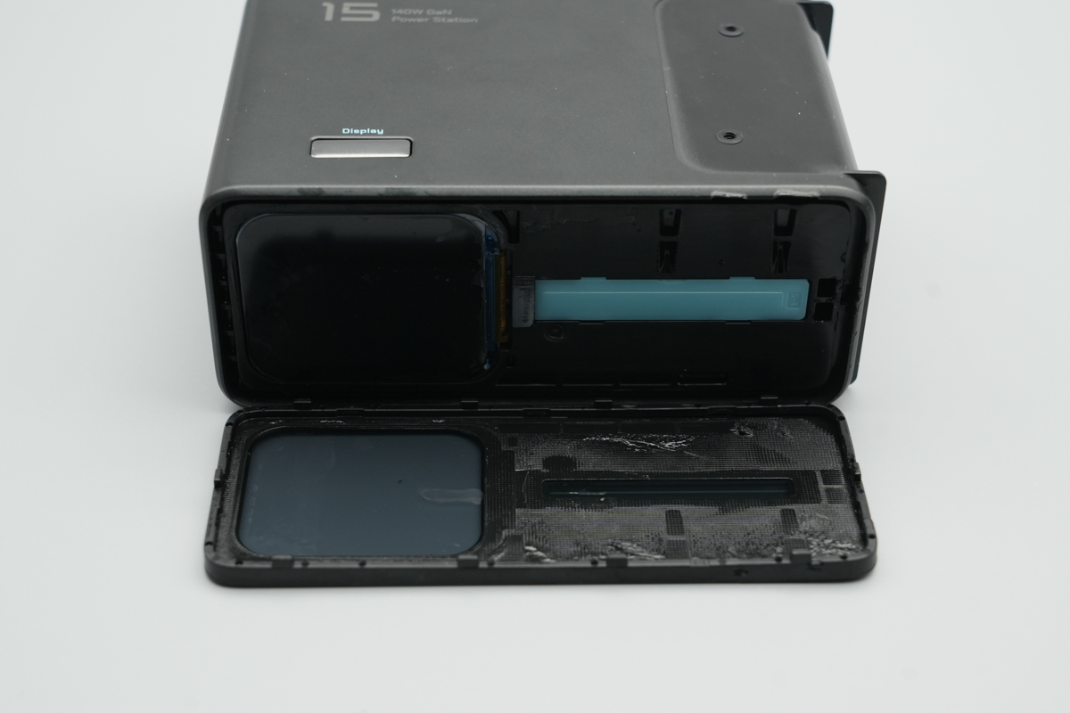
The body features a spliced design, with an LCD screen on the left and output ports at the bottom. The upper right section houses the wireless charging area, while the retractable cable is located below it.

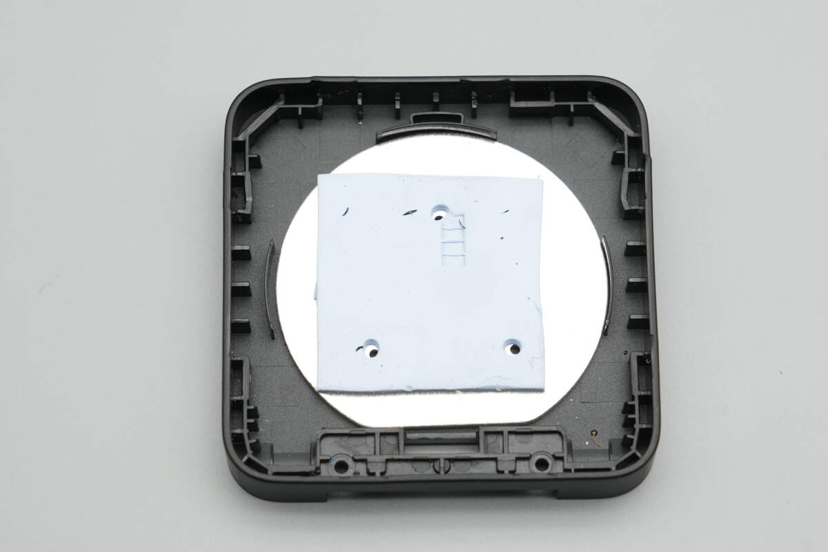
The top wireless charging panel has a usage instruction label attached.
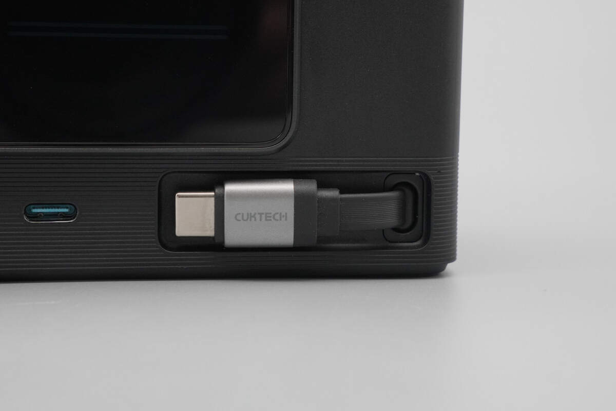
The retractable cable plug has a metal casing, is secured magnetically, and is marked with “CUKTECH.”
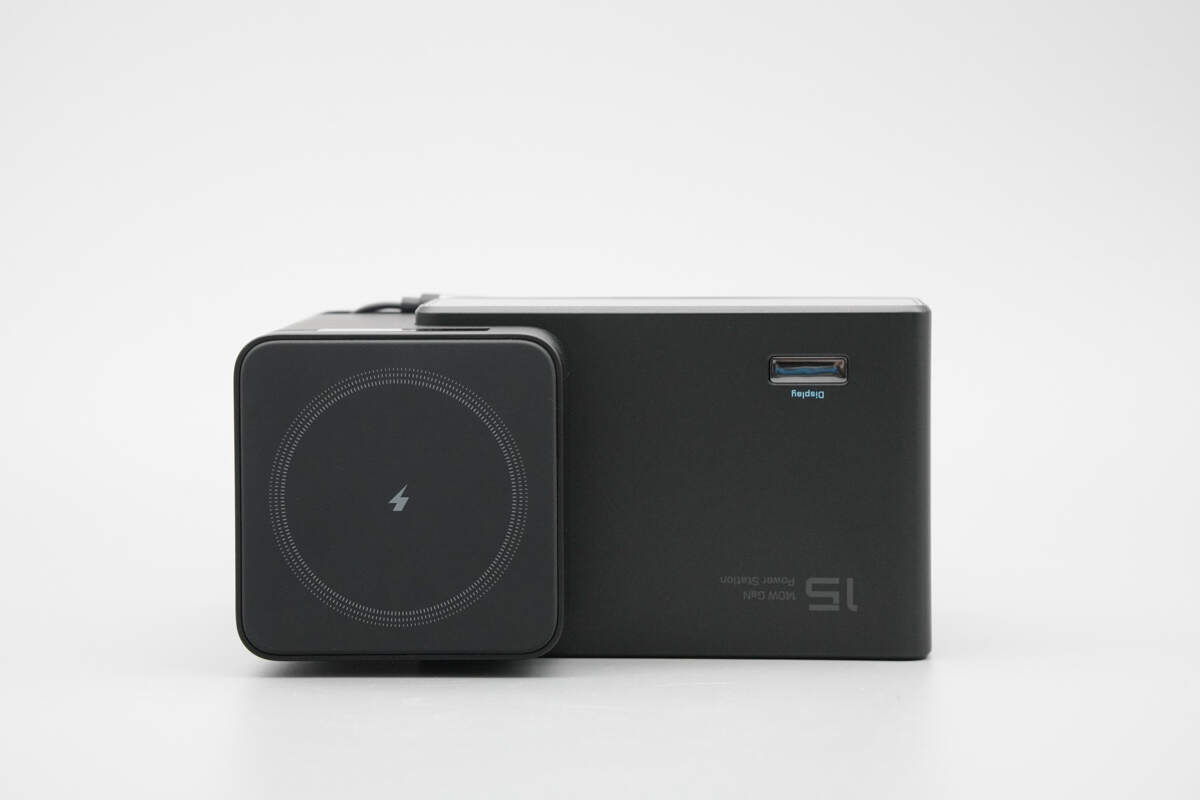
In addition to the wireless charging area, the top also features a button for controlling the display.

Close-up of the button.
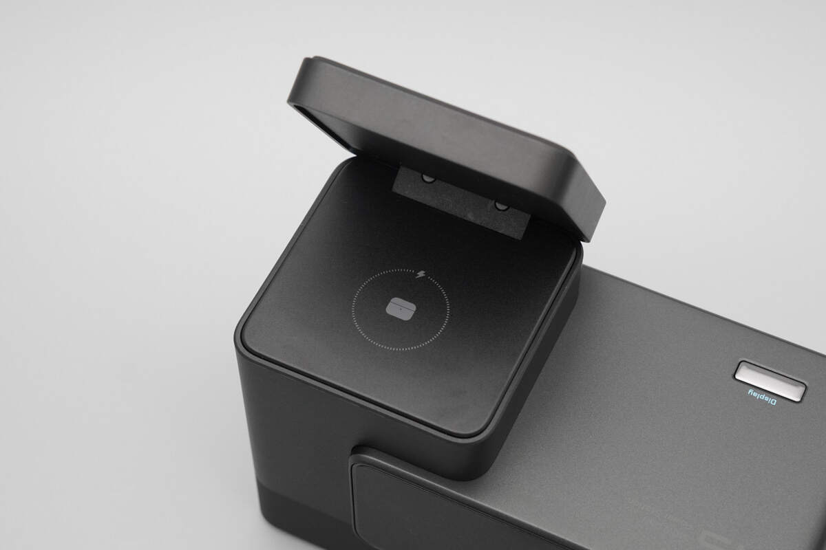
Beneath the magnetic wireless charging panel, there is an additional wireless charging area.
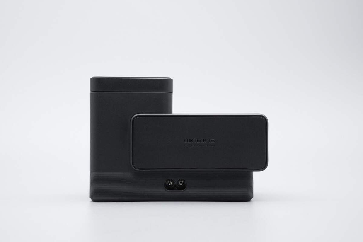
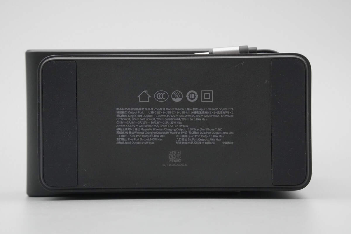
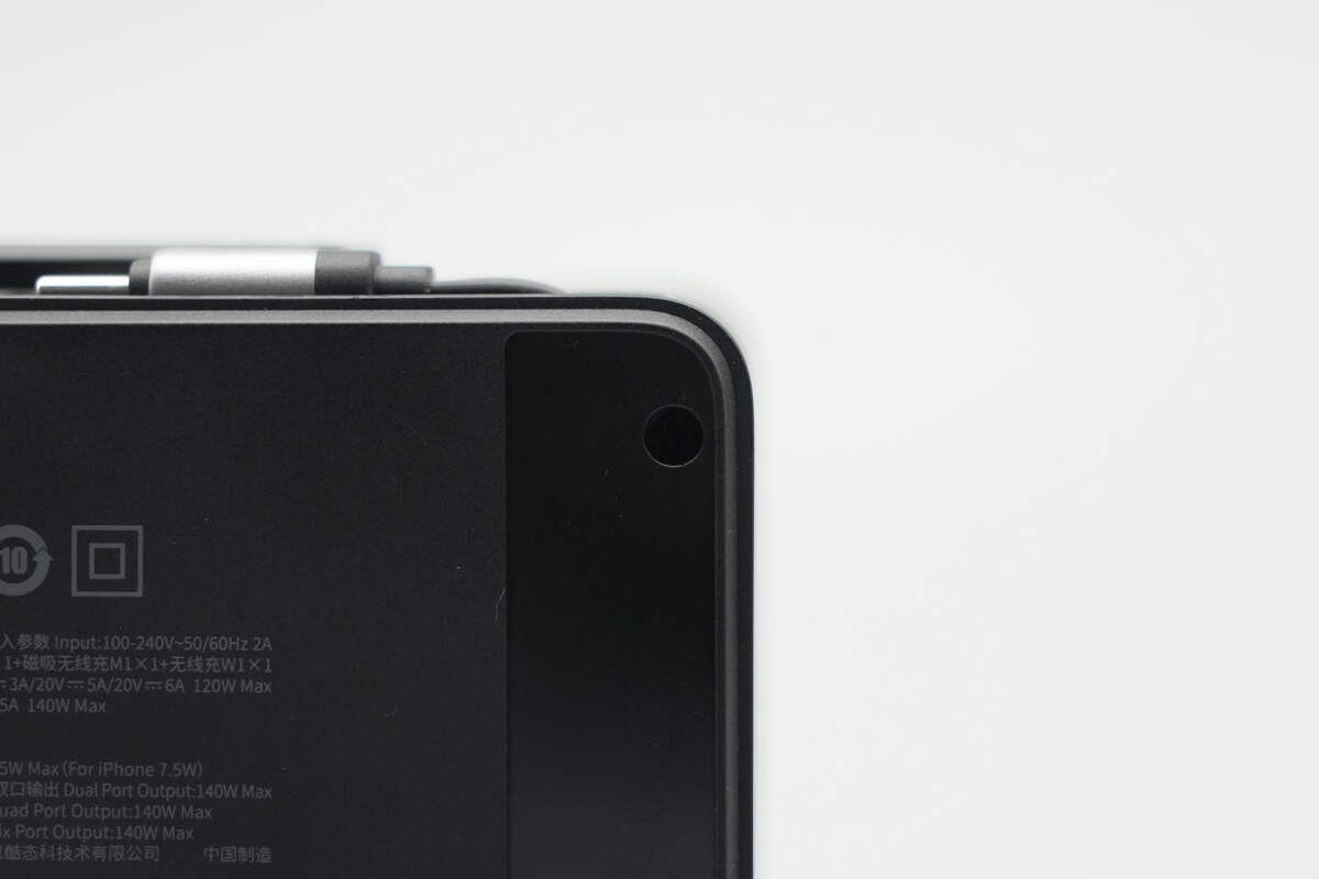
The back of the device features a C7 power input socket.
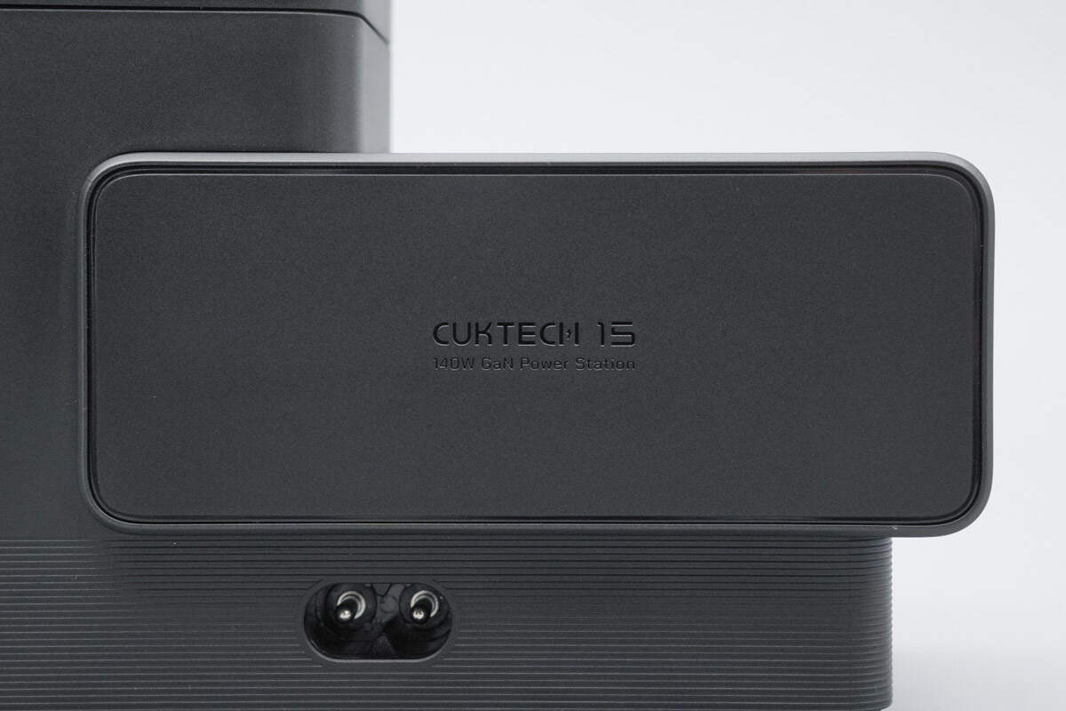
The back is engraved with “CUKTECH 15.”
Side view of the device.
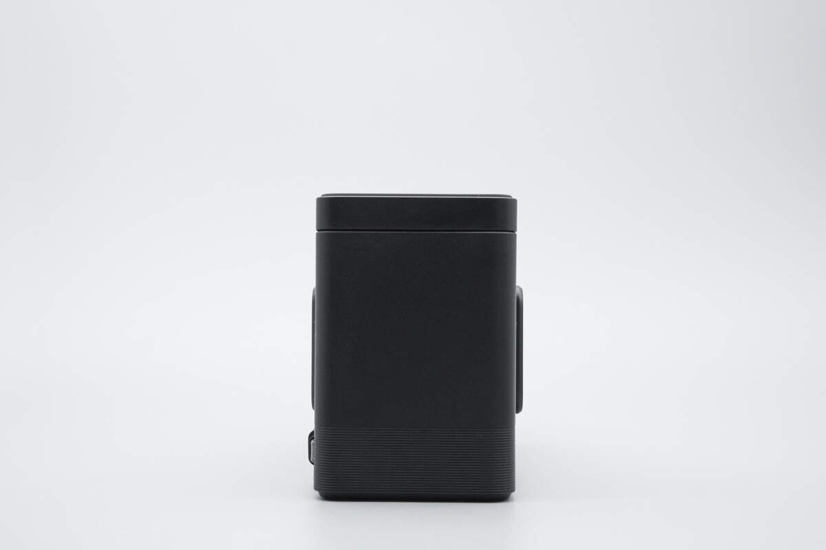
View of the opposite side.
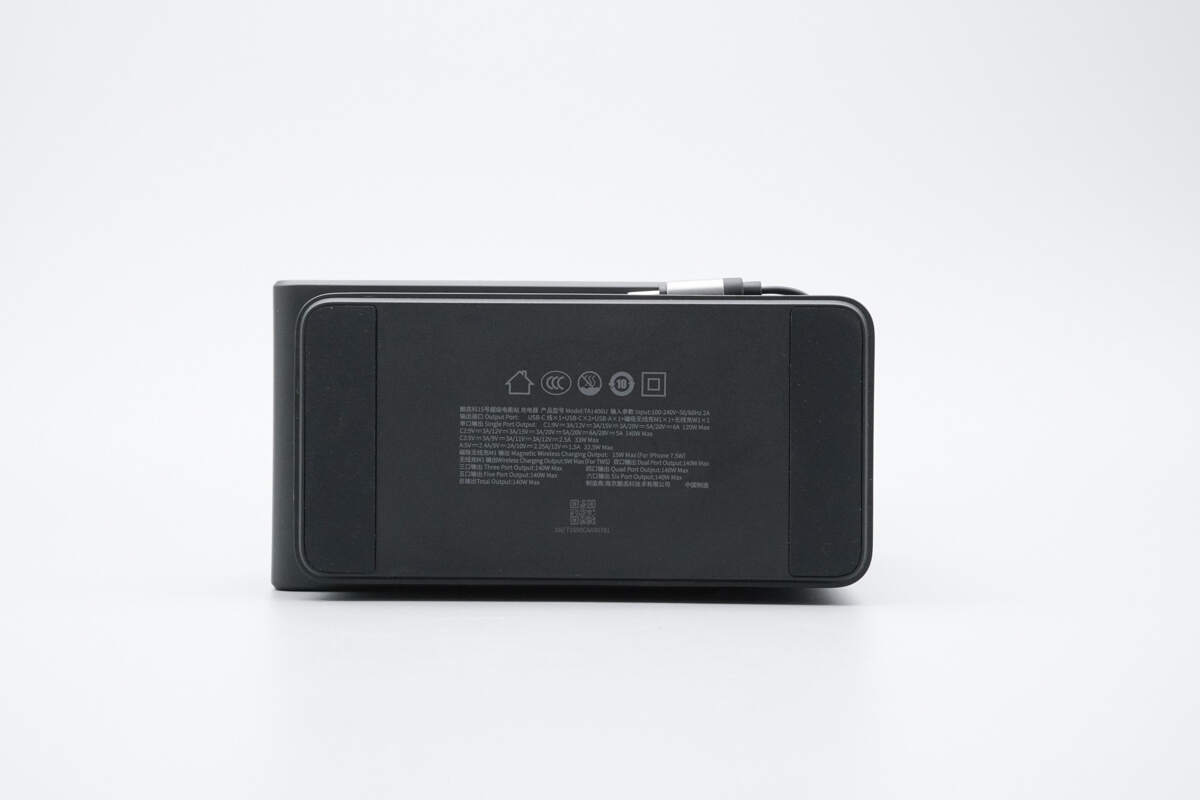
The bottom has anti-slip pads and displays the technical specifications.
Model: TA1406U
Input: 100-240V~ 50/60Hz 2A
Output Ports: USB-C Cable*1 + USB-C*2 + USB-A*1 + Magnetic Wireless Charging M1*1 + Wireless Charging W1*1
Single Port Output:
C1: 9V⎓3A / 12V⎓3A / 15V⎓3A / 20V⎓5A / 20V⎓6A, 120W Max
C2: 9V⎓3A / 12V⎓3A / 15V⎓3A / 20V⎓5A / 28V⎓5A, 140W Max
C3: 5V⎓3A / 9V⎓3A / 11V⎓3A / 12V⎓2.5A, 33W Max
A: 5V⎓2.4A / 9V⎓2A / 10V⎓2.25A / 12V⎓1.5A, 22.5W Max
Magnetic Wireless Charging M1 Output: 15W Max (for iPhone 7.5W)
Wireless Charging W1 Output: 5W Max (for TWS)
Total Output: 140W Max
The product has passed CCC certification.
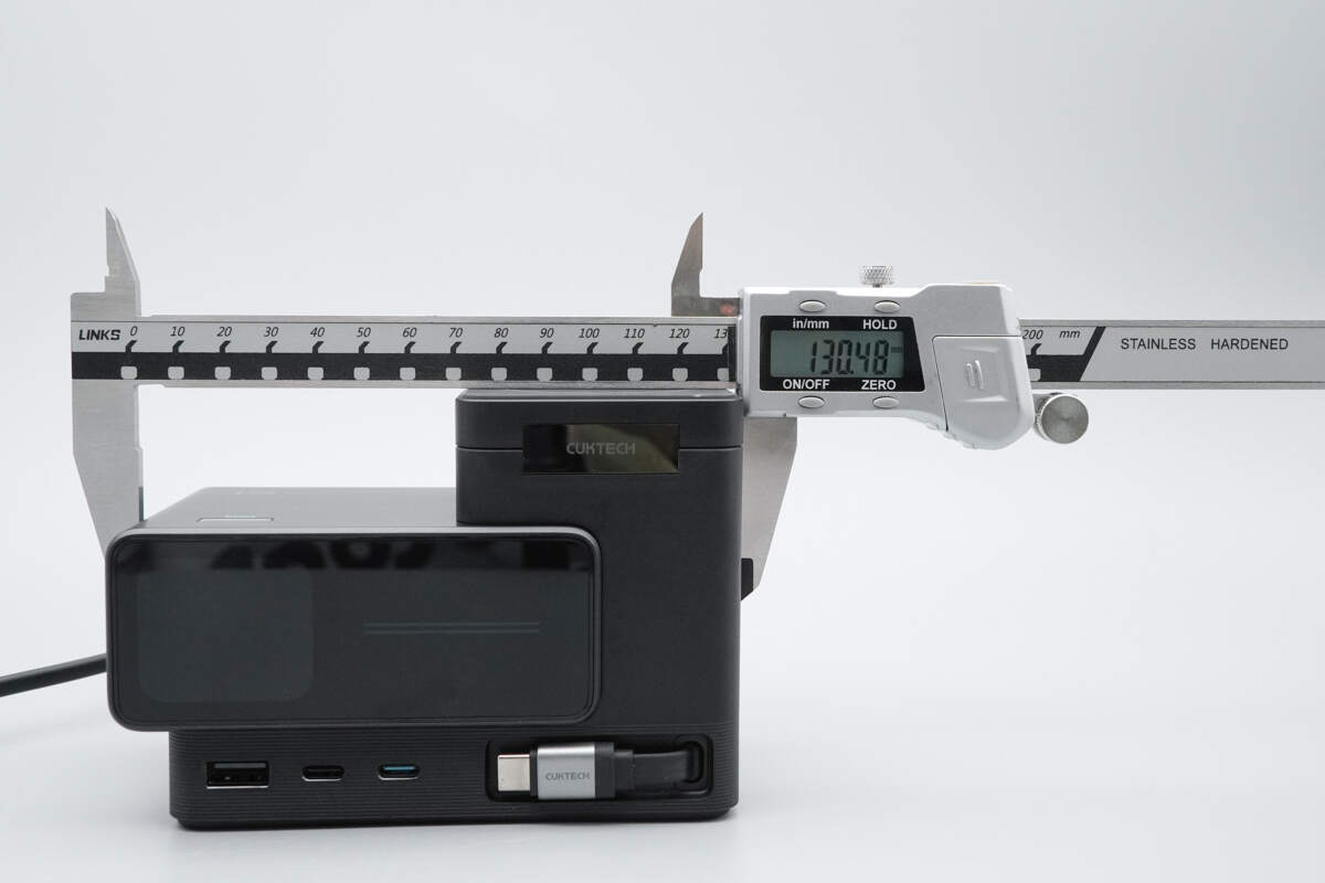
The width of the charging station is about 130.5 mm (5.14 inches).

The height is about 90.3 mm (3.56 inches).

The thickness is about 68.3 mm (2.69 inches).
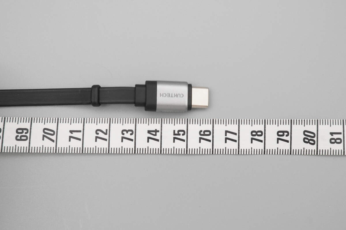
The length of the USB-C retractable cable is about 76 cm (29.92 inches).
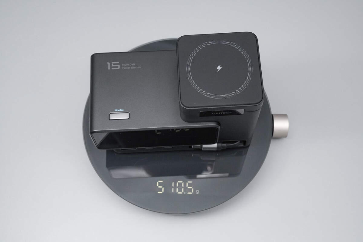
The weight is about 510.5 g (18.0074 oz).
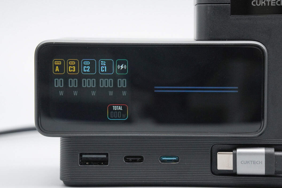
When powered on, the screen lights up and shows all port outputs and total output as 0W.

The magnetic wireless charging function can be turned on or off.
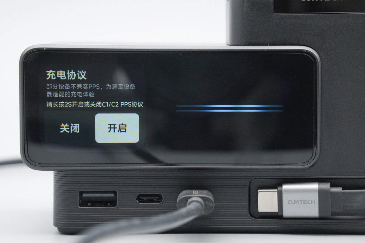
It also allows control of the PPS charging protocol on or off.
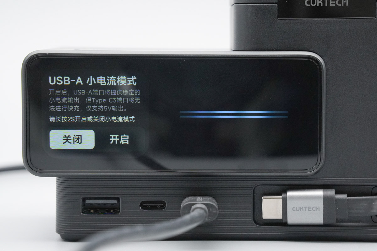
The USB-A port features a switch for low-current mode.
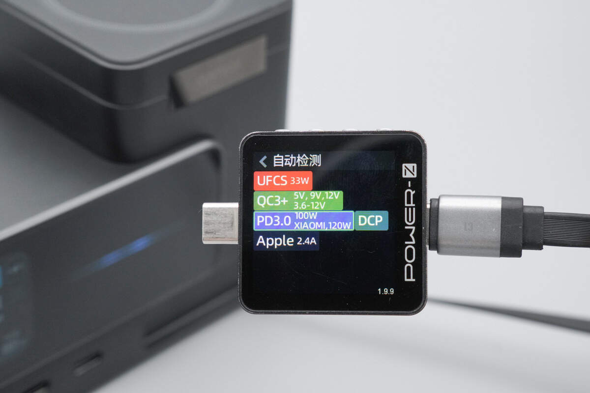
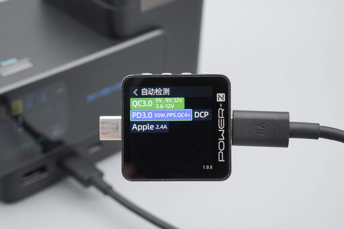
ChargerLAB POWER-Z KM003C shows that the USB-C1 retractable cable supports UFCS, QC3+, PD3.0, Xiaomi 120W, DCP, and Apple 2.4A charging protocols.

It has five fixed PDOs of 5V3A, 9V3A, 12V3A, 15V3A, and 20V5A, as well as two Xiaomi proprietary voltage levels: 5–11V6A and 5–20V6A.

The USB-C2 supports QC3+, PD3.1, Xiaomi 100W, DCP, and Apple 2.4A protocols.
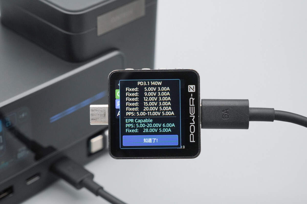
It has six fixed PDOs of 5V3A, 9V3A, 12V3A, 15V3A, 20V5A, and 28V5A. It also has two sets of PPS, which are 5-11V5A and 5-20V6A.
The USB-C3 supports QC3.0/4+, PD3.0, PPS, DCP, and Apple 2.4A protocols.
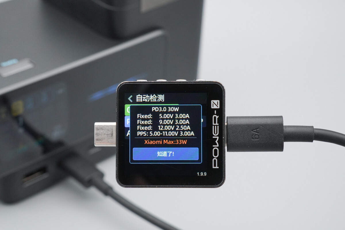
It has three fixed PDOs: 5V3A, 9V3A, and 12V2.5A, and also supports Xiaomi 33W fast charging protocol.
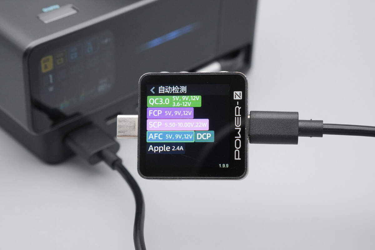
The USB-A supports QC3.0, FCP, SCP, AFC, DCP, and Apple 2.4A protocols.
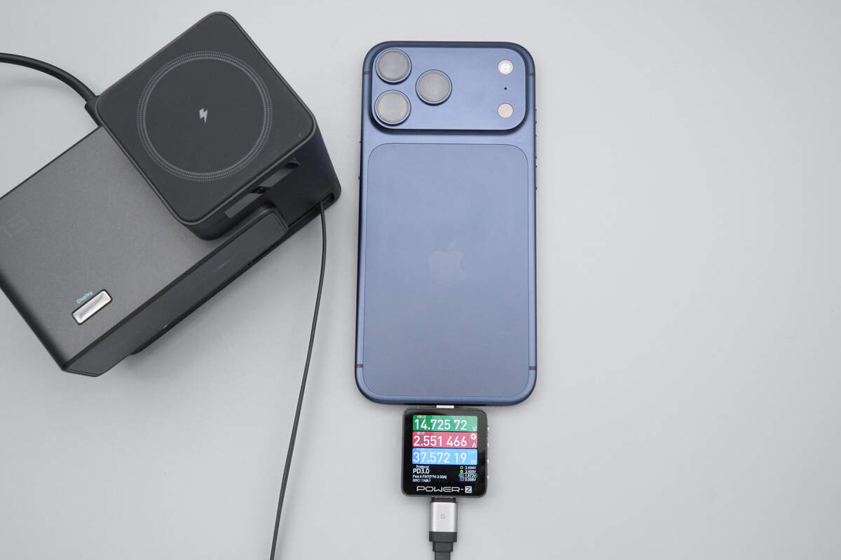
Using the built-in cable to charge an iPhone 17 Pro Max, the input power is about 37.6W.
Using the magnetic charging panel to charge the iPhone 17 Pro Max, the display shows a power output of 7.1W.

It can wirelessly charge an iPhone 17 Pro Max and AirPods 4 simultaneously.
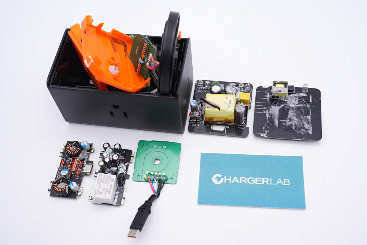
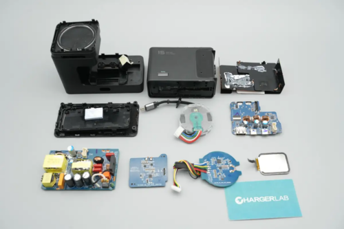
Teardown
Next, let's take it apart to see its internal components and structure.
Peel off the anti-slip pads on the bottom and unscrew the fixing screws.
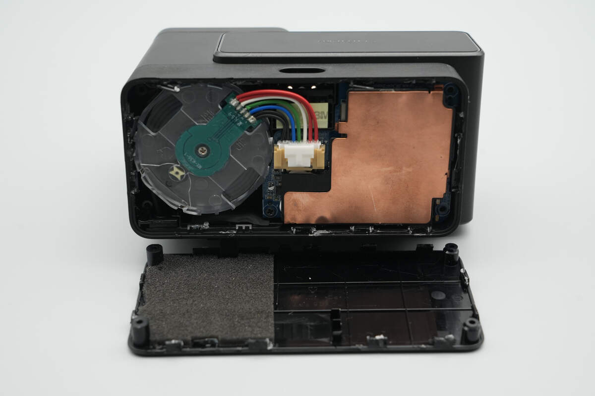
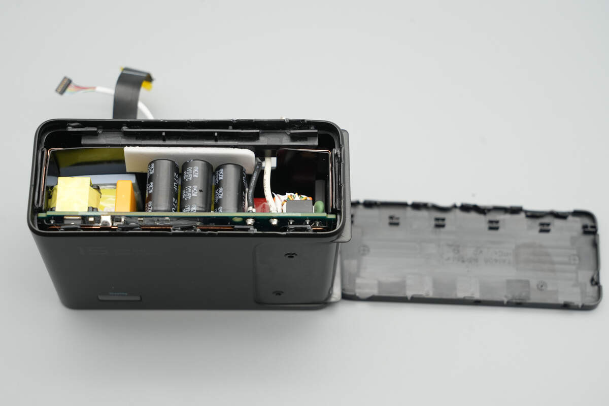
Pry open the back cover along the seam. It is secured with clips and adhesive.
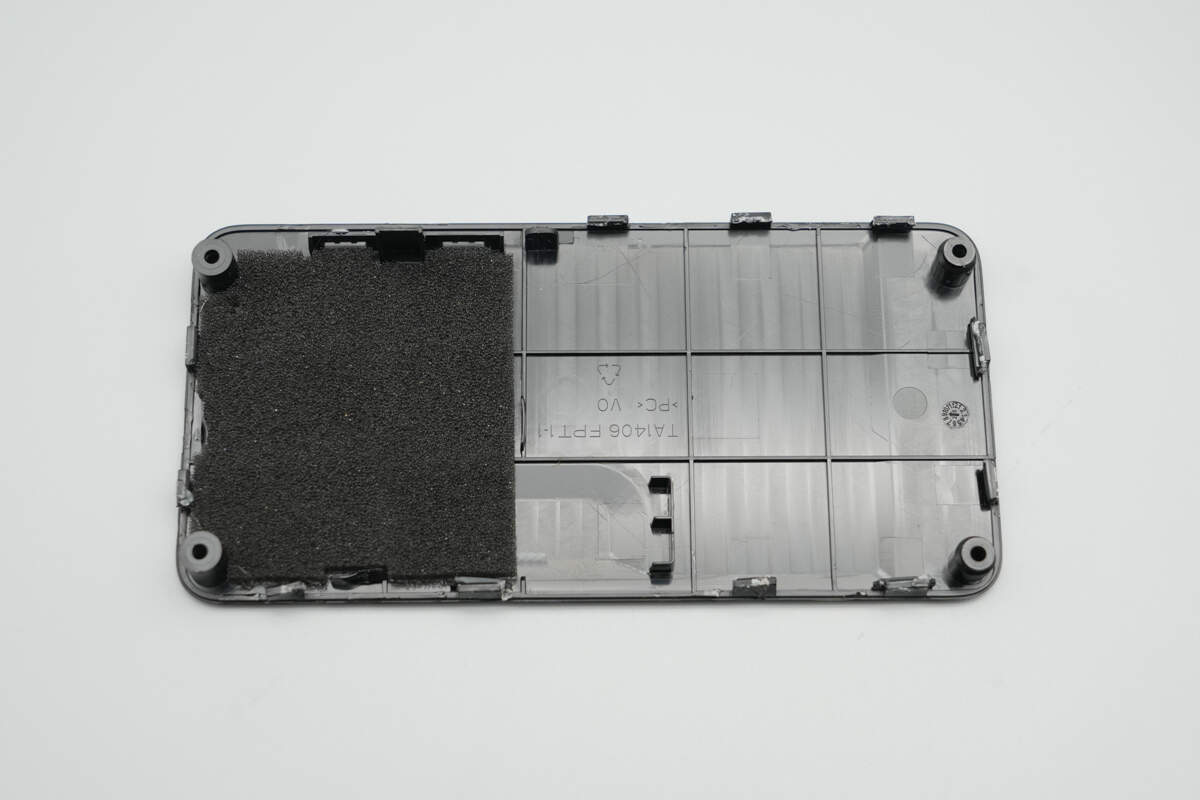
The inner side of the back cover has cushioning foam corresponding to the position of the PCBA module.
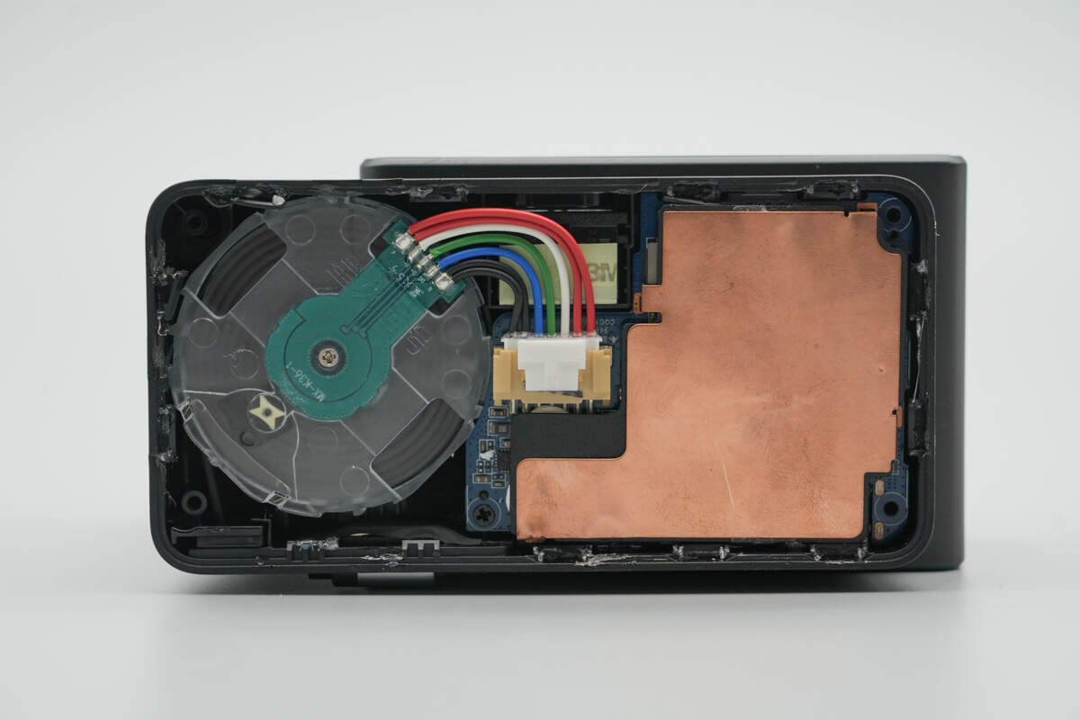
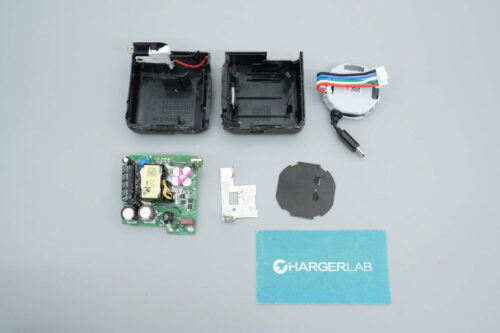
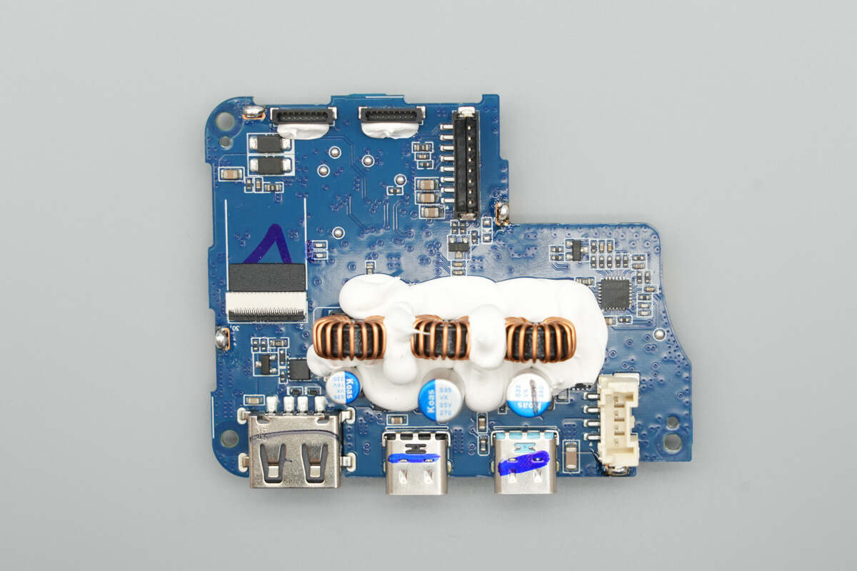
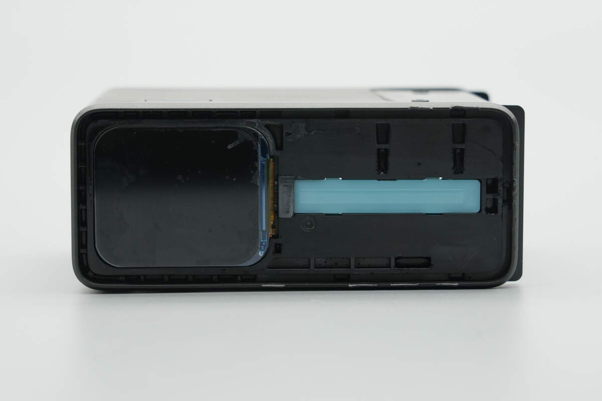
The left side houses the retractable cable module, while the right side contains the PCBA module, which is covered with a copper sheet for enhanced heat dissipation. The retractable cable module is connected to the PCBA module via a connector.
Remove the PCBA module at the bottom, which is connected via wires and connectors.

Remove the PCBA module and the retractable cable module.
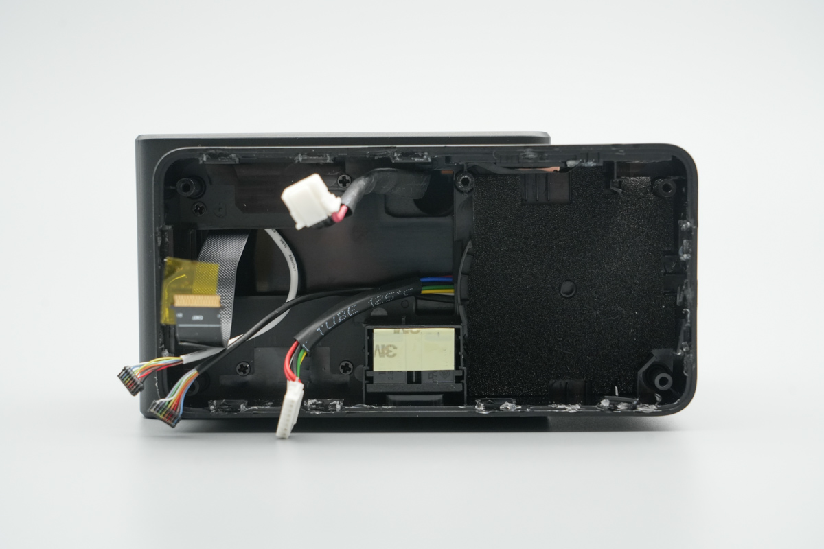
Inside, there are connecting cables.

There are screws underneath the cushioning foam.

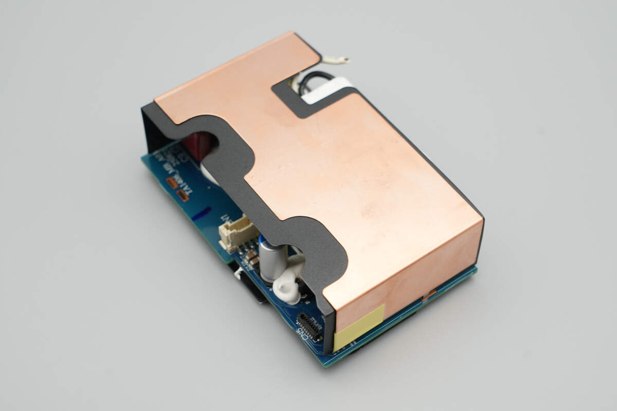
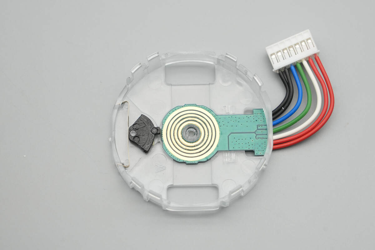
Remove the wireless charging cover, and inside is the PCBA module and the wireless charging coil.
The lower layer of the PCBA module is equipped with a thermal pad for heat dissipation.

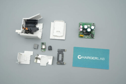
Remove the magnetic wireless charging module and the display module.
Remove the cover of the display, and inside you'll find another PCBA module.
The PCBA module is covered with copper sheets, and there are Mylar sheets inside for insulation.

The length of the PCBA module is about 94.4 mm (3.72 inches).

The width is about 59.5 mm (2.34 inches).

The thickness is about 29.1 mm (1.15 inches).
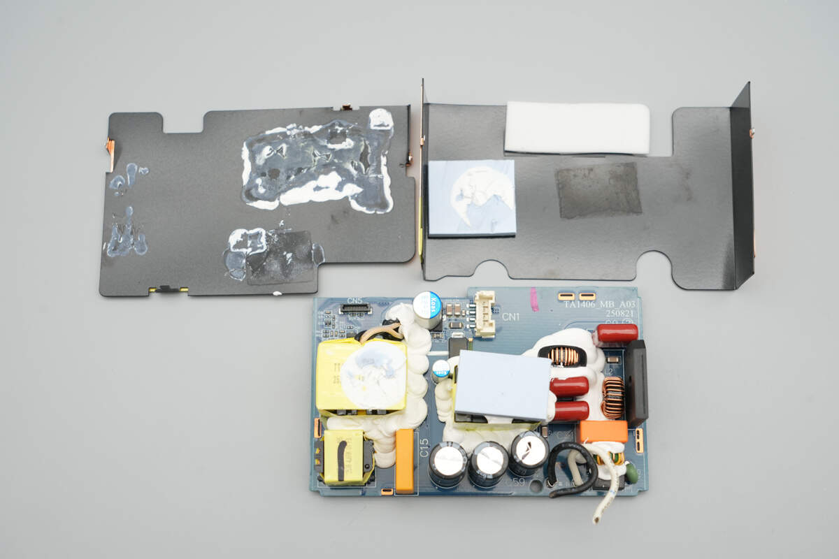
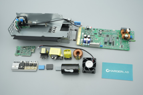
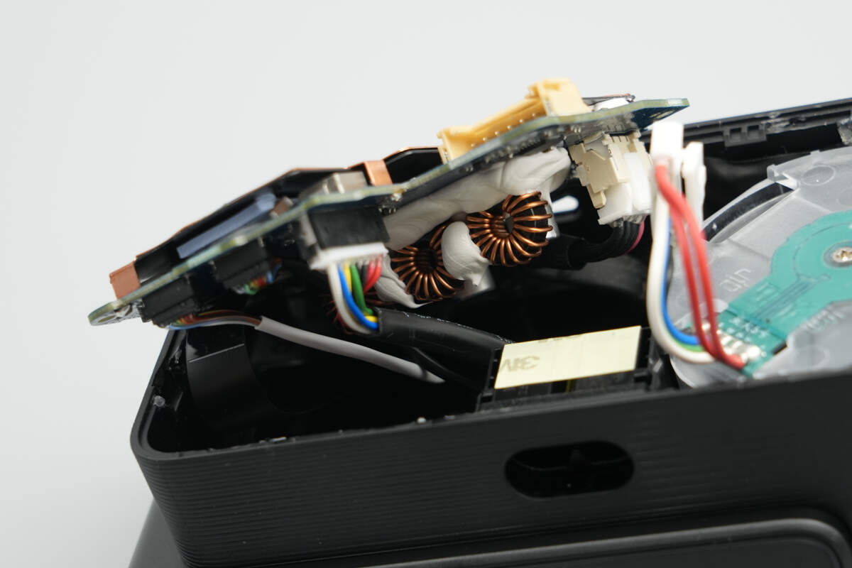
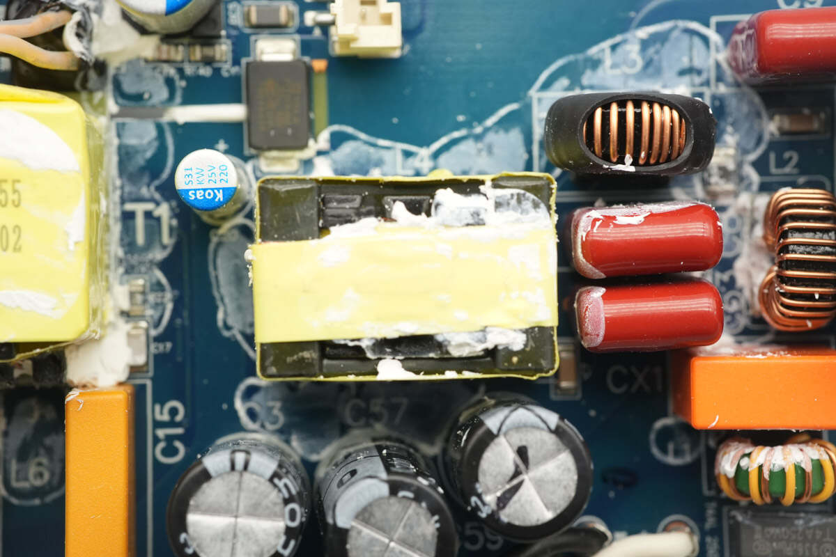
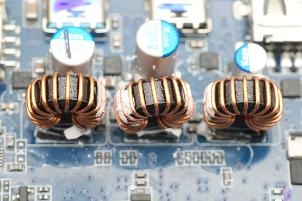
Remove the heatsinks. The PFC boost inductor and LLC transformer are attached with thermal pads for heat dissipation, and adhesive is applied between the components for reinforcement.
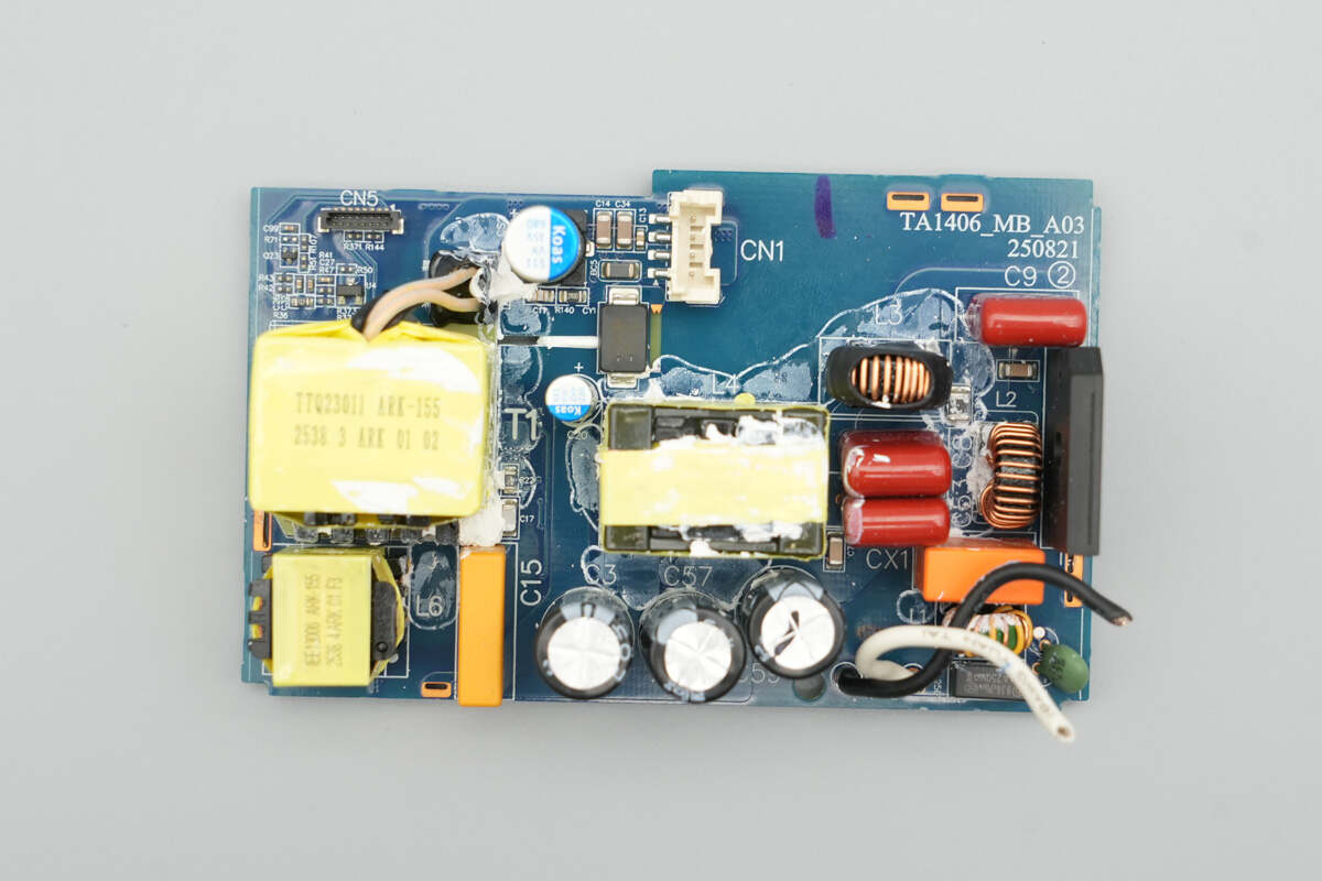
The front of the PCBA module features a fuse, NTC thermistor, common mode choke, safety X2 capacitor, bridge rectifier, film capacitors, filter inductors, PFC boost inductor, high-voltage filter capacitors, LLC transformer, resonant inductor, resonant capacitor, and a solid capacitor.

The back features a PFC rectifier, master control chip, PFC MOSFET, LLC MOSFETs, SMD Y capacitors, optocouplers, synchronous rectifier controller, and synchronous rectifiers.

The input fuse is from Betterfuse, with part number 936, and is rated at 4A, 250V.

The NTC thermistor, marked with SCK012A, is used to suppress inrush current during power-on.

The common mode choke is wound using enamel-coated wire and insulated wire.
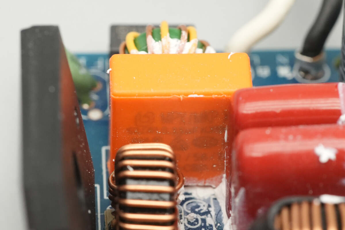
The safety X2 capacitor is from Surong, with a specification of 0.33μF.
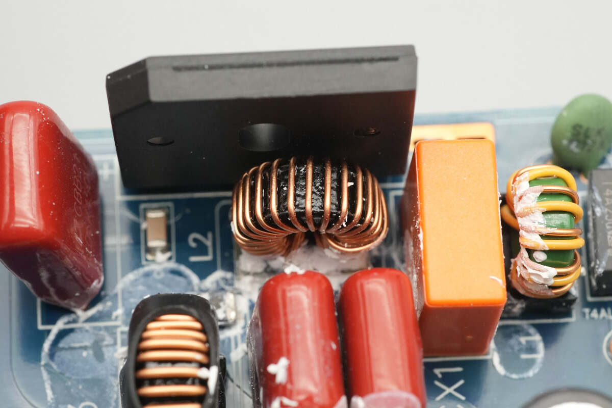
The filter inductor is wound using enamel-coated wire.

The bridge rectifier is from YJ, model GBU1510, with a specification of 1000V, 15A, and is packaged in a GBU form factor.
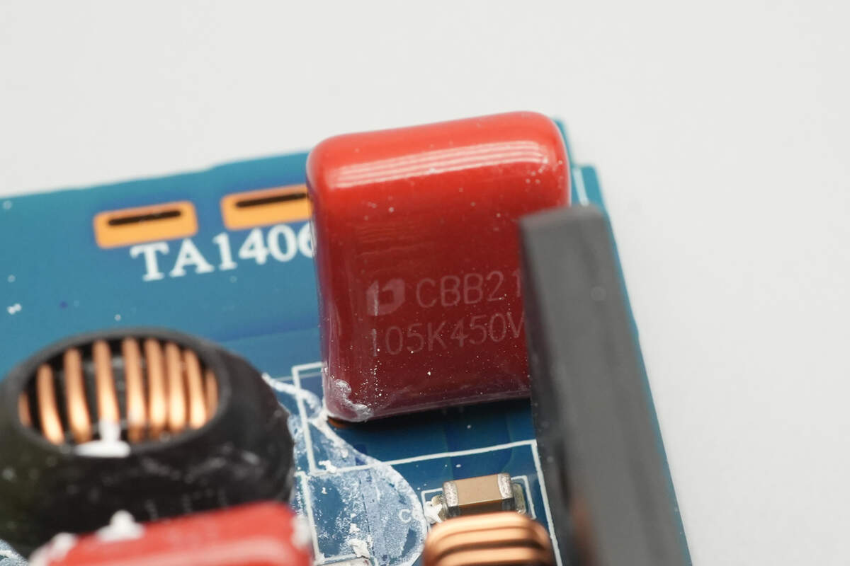
The film capacitor is from Surong, part of the CBB21 series, with a specification of 1μF, 450V.
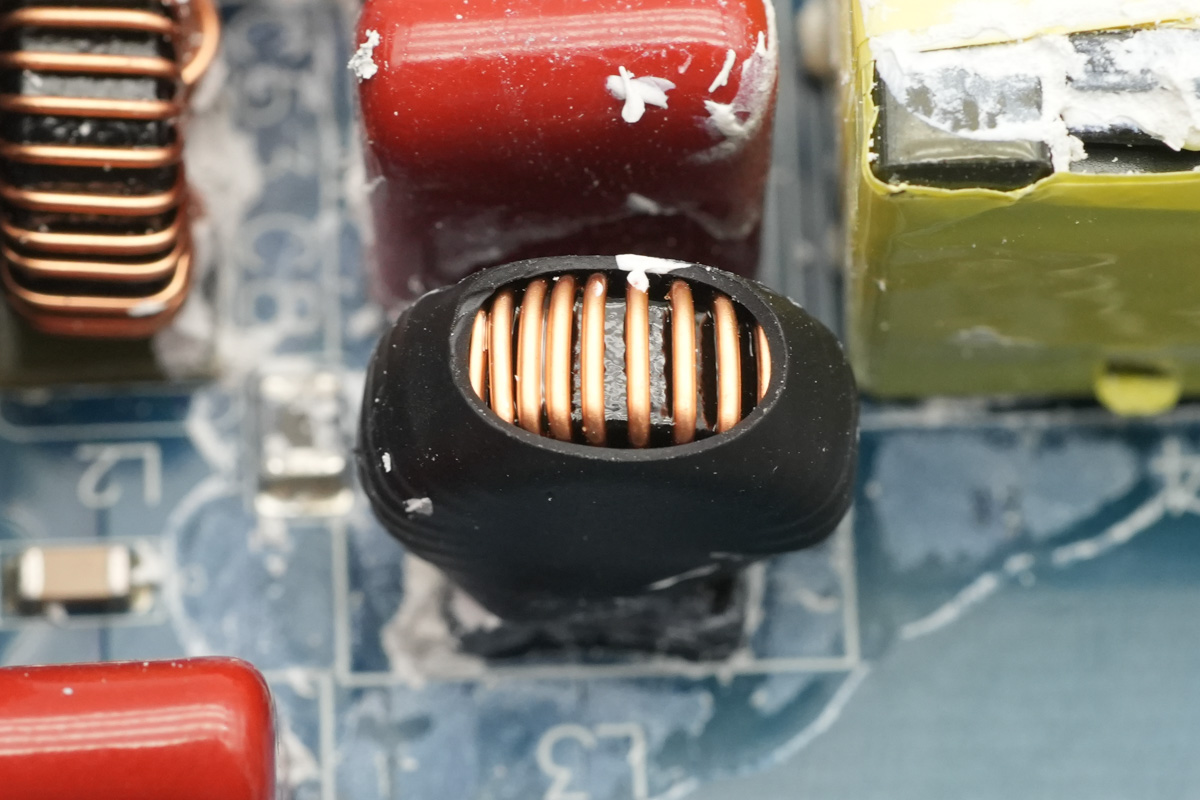
The filter inductor is wound with enamel-coated wire and insulated with heat shrink tubing.

The two film capacitors have a specification of 1μF, 450V each.

The primary controller chip is from MPS, with a custom model marked as CD1271. It is a PFC+LLC dual-function controller, packaged in an SOIC-16 form factor.
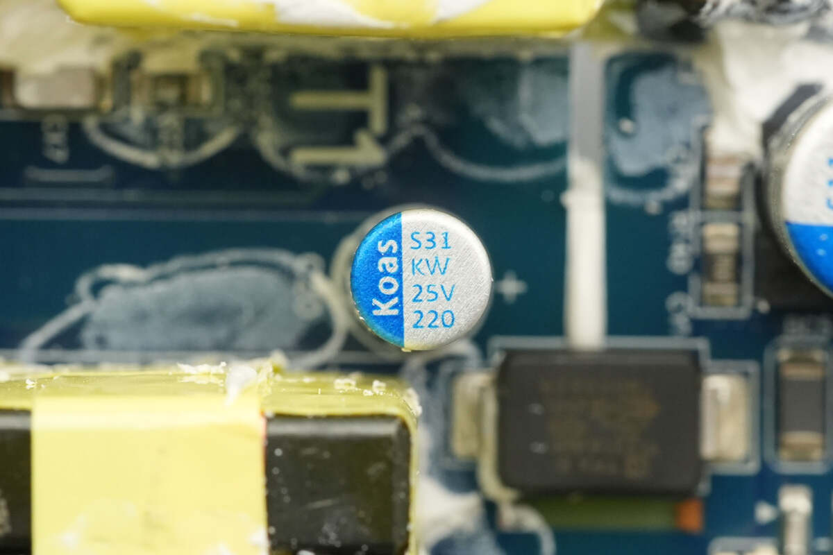
The filter capacitor that powers the master control chip is from Koshin, part of the KW series. It is a high-temperature, 125°C-rated polymer conductive solid capacitor, with a specification of 25V, 220μF.
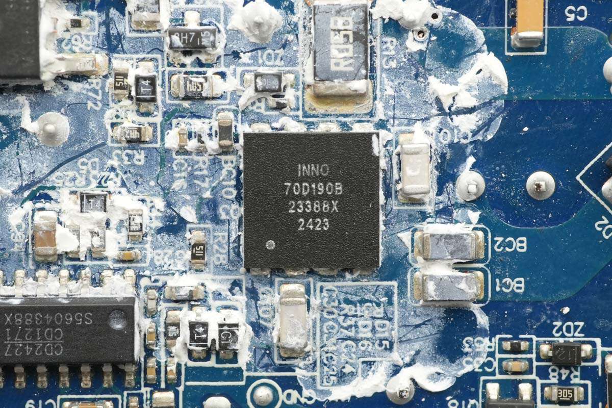
The PFC MOSFET is from Innoscience, model INN700D190B. This is a 700V-rated enhanced GaN transistor, upgraded from its original 650V rating to 700V, with a transient voltage rating of 800V. The device has a Rds(on) of 190mΩ and supports higher power applications.
The INN700D190B supports ultra-high switching frequencies, has no reverse recovery charge, and features very low gate charge and output charge. It complies with JEDEC standards for industrial applications and includes built-in ESD protection. The component is RoHS-compliant, lead-free, and conforms to EU REACH regulations, making it suitable for high-efficiency, high-density applications like AC-DC and DC-DC conversion. It comes in a DFN8*8 package.
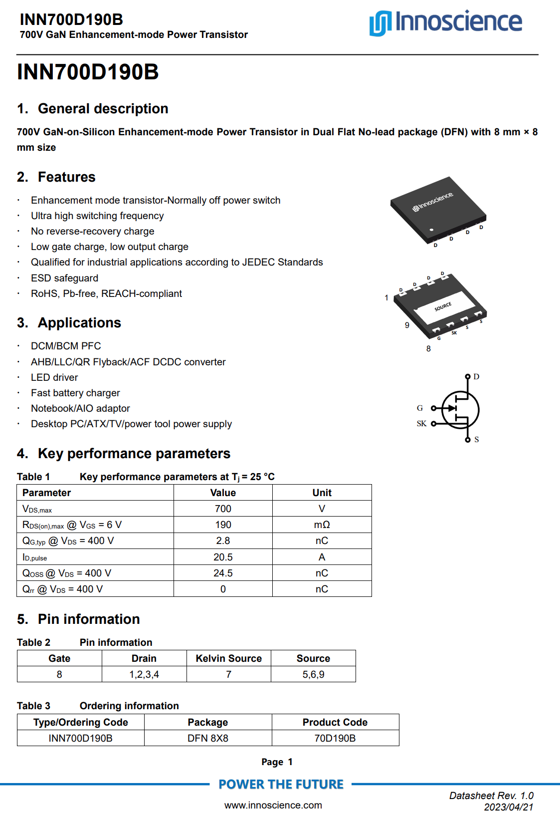
Here is the information about Innoscience INN700D190B.
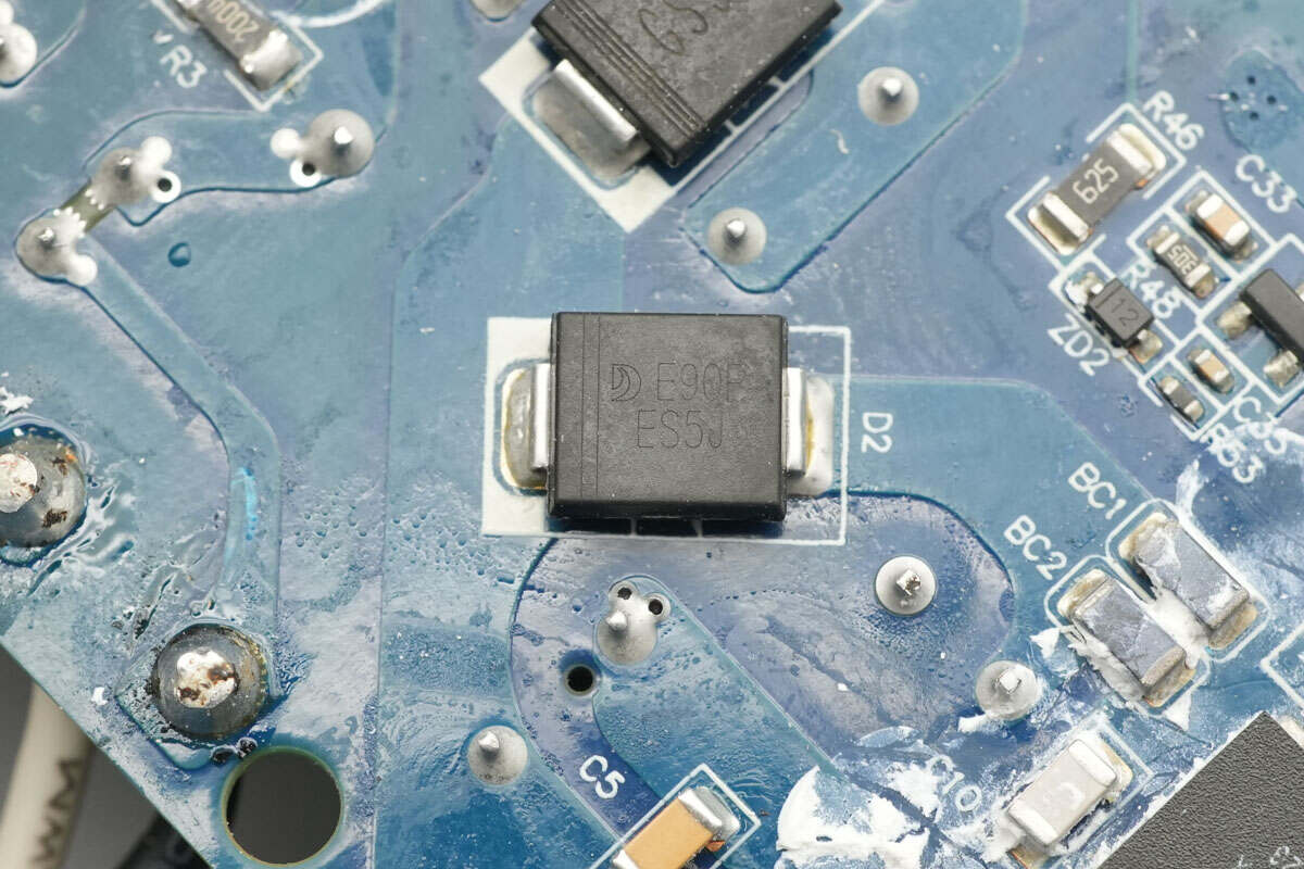
The PFC rectifier is from Jingdao Microelectronics, model ES5JCC. It is an ultra-fast recovery diode, with a specification of 600V, 5A, and is packaged in an SMC-C form factor.
Close-up of the PFC boost inductor.
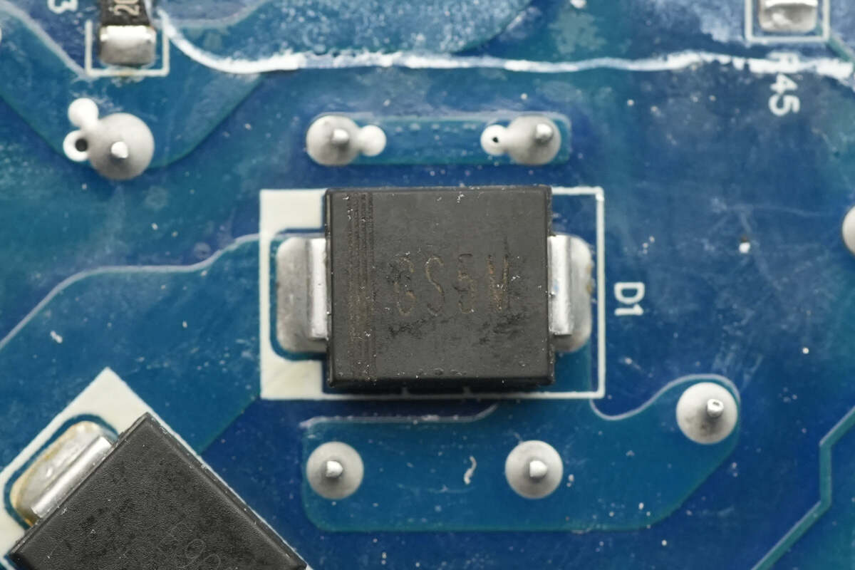
The PFC bypass diode is model GS5M.

The high-voltage filter capacitors are connected in parallel, with a total of three capacitors.
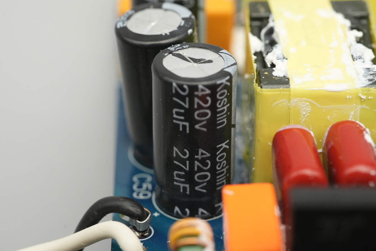
The capacitors are from Koshin, with a specification of 420V, 27μF.

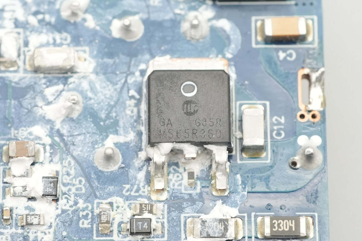
The LLC MOSFET is from HWDZ, model MS65R360. It is an NMOS transistor with a voltage rating of 650V, an Rds(on) of 400mΩ, and comes in a DPAK package.
The other MOSFEThas the same model number.

The resonant capacitor is from WQC, part of the MMKP82 series, with a specification of 0.022μF, 630V.
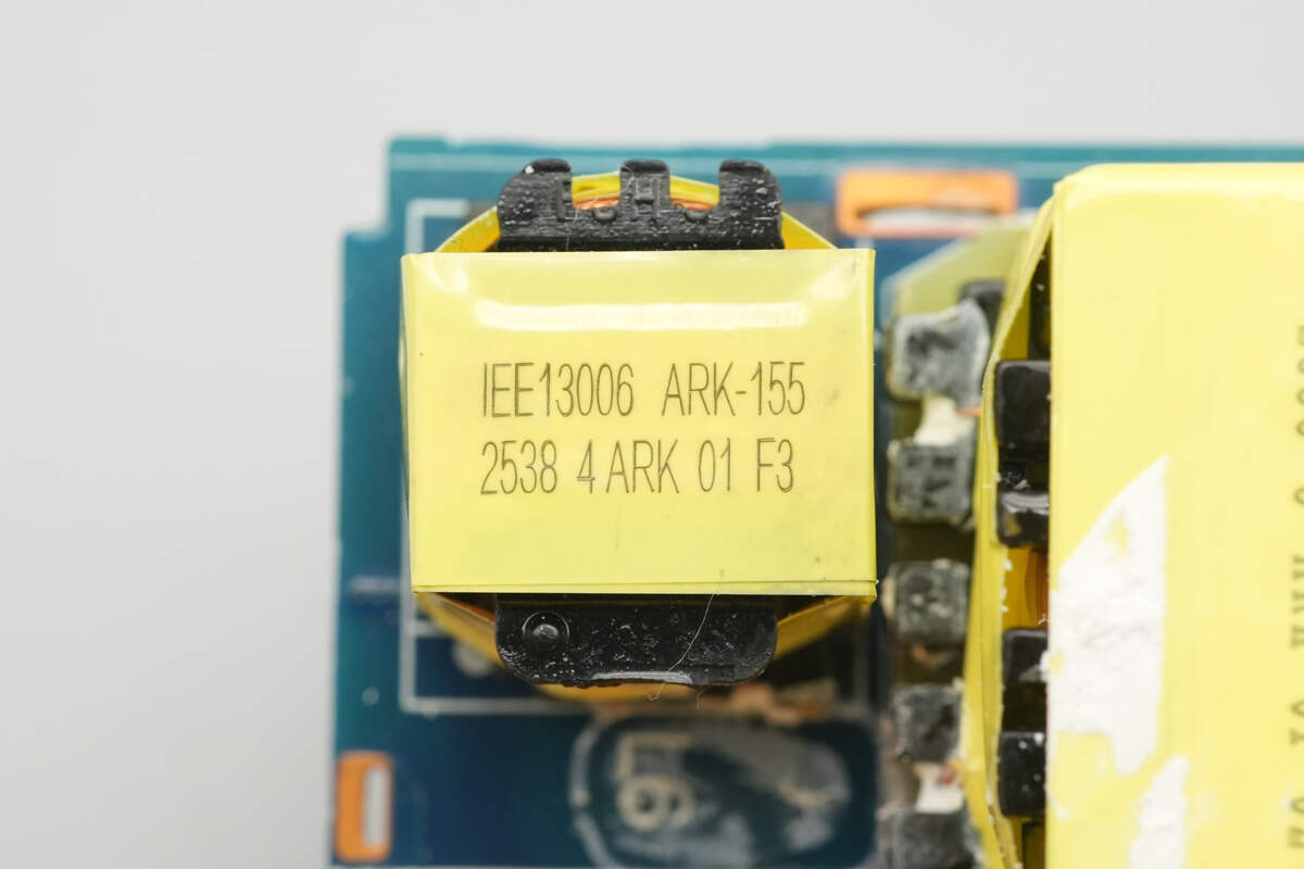
Close-up of the LLC resonant inductor.

The LLC transformer is tightly wrapped with insulating tape for insulation.
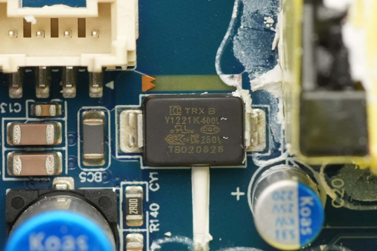
The SMD Y capacitor is from TRX, with part number TMY1221K. Its compact size and lightweight design make it ideal for high-density power products, such as GaN fast chargers.

The other SMD Y capacitor has the part number TMY1331K.

The optocoupler is from OR, model OR1008, and is used for output voltage feedback.
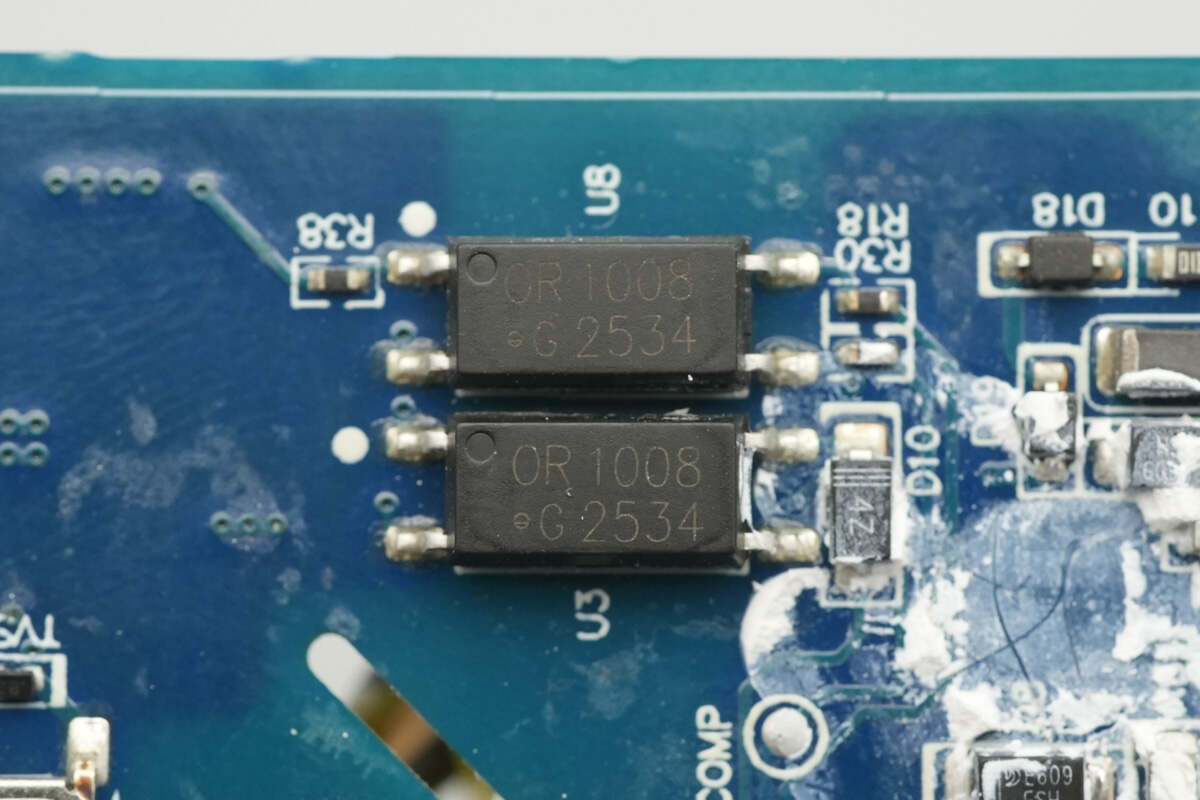
The other two optocouplers are used for isolation communication.

The synchronous rectifier controller is from MPS, model MP6925. It is a dual-channel fast turn-off rectifier, designed for LLC switch-mode power supplies. It supports both standard and logic-level synchronous rectifier transistors, with an operating voltage range of 4.2-35V. The controller supports CCM, CrCM, and DCM operating modes, as well as high-side and low-side applications. It is packaged in an SOIC-8 form factor.

The synchronous rectifiers are from Vergiga, marked with 6R10NM, and are packaged in a PDFN5*6 form factor.
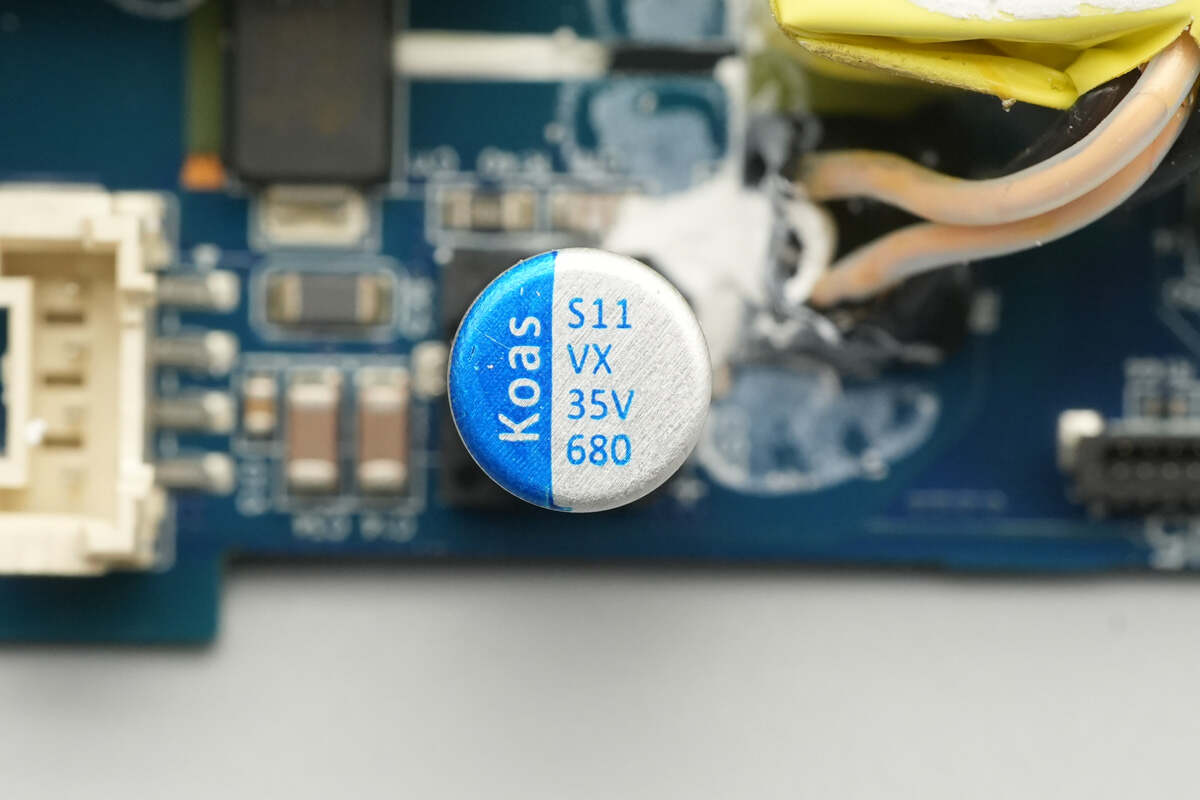
The solid capacitor is from Koshin, part of the VX series, a 125°C-rated high-temperature polymer conductive solid capacitor. It has a specification of 35V, 680μF.
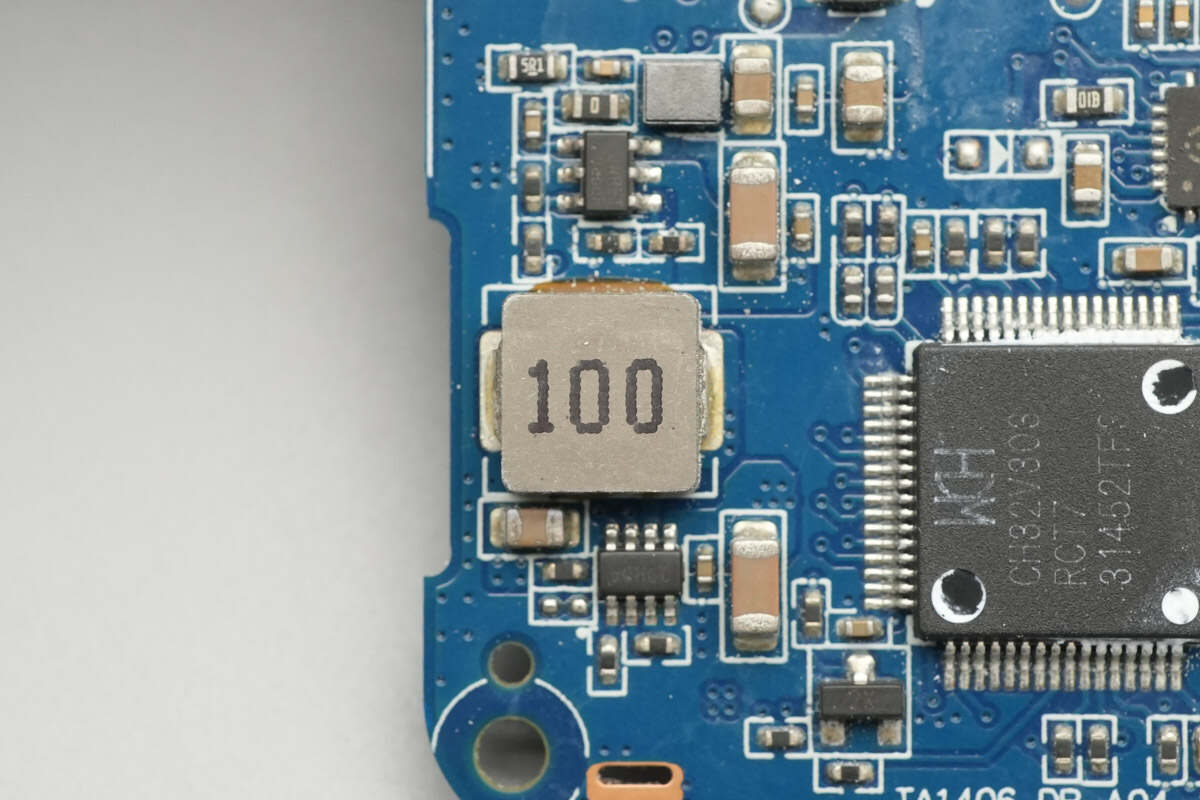
The components on the front of the secondary buck converter PCB are reinforced with adhesive.

The back has a copper sheet and a layer of Mylar sheet.
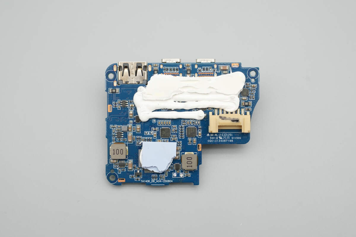
Remove the copper sheet and Mylar sheet. Inside, there is thermal adhesive and a thermal pad for heat dissipation.
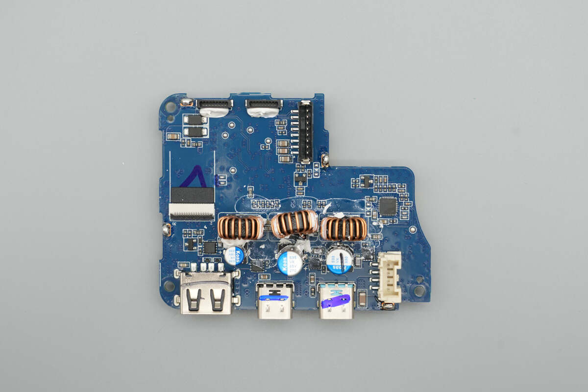
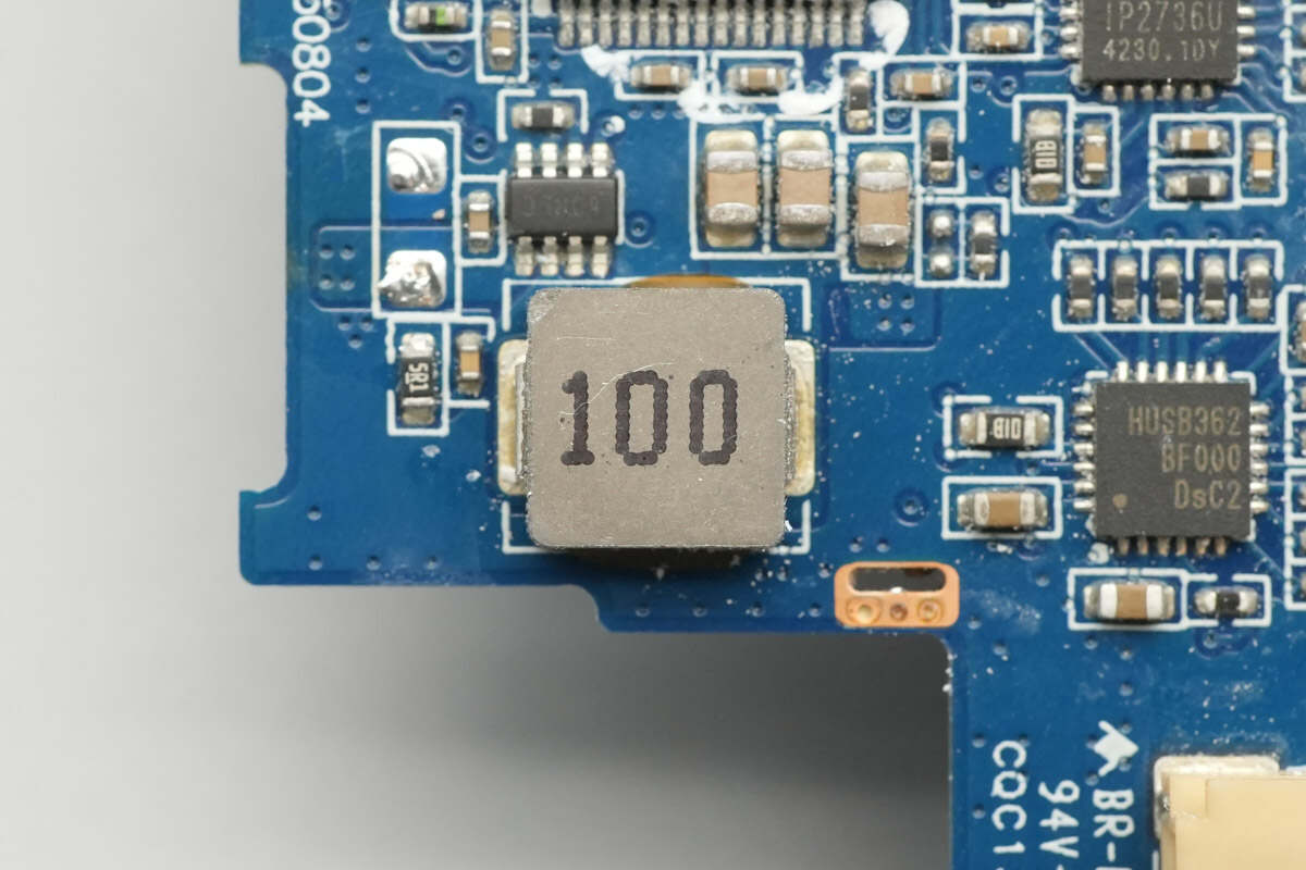
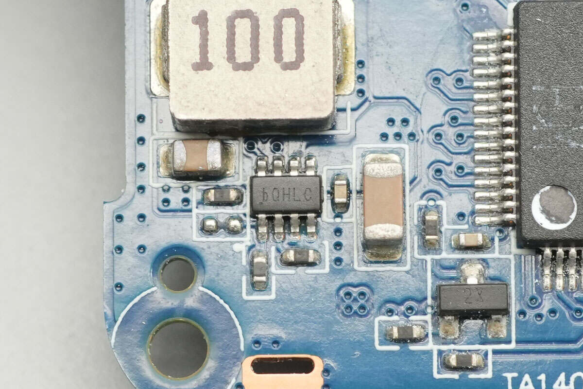
The front features three buck inductors and filter capacitors, along with USB-C and USB-A sockets. It also includes a protocol chip.

The back side contains the MCU, protocol chips, synchronous buck controllers, and buck MOSFETs.
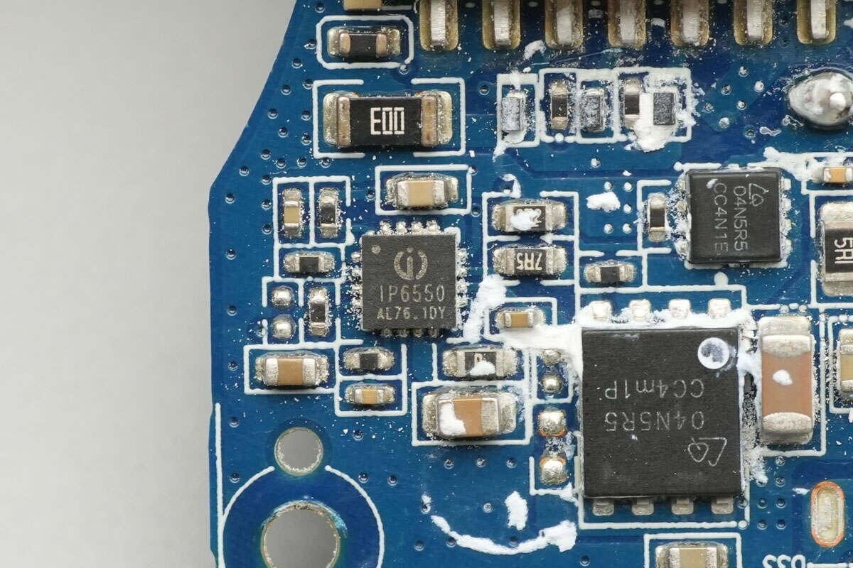
The synchronous buck controller is from Injoinic, model IP6550. It supports a 36V input and features an integrated NMOS driver, with two external MOSFETs for efficient synchronous rectification and step-down conversion. The switching frequency is 135kHz, and the input voltage rating is 48V. It also includes comprehensive protection features. The controller comes in a 3x3mm QFN16 package, which simplifies the design of synchronous buck conversion circuits.
The IP6550 is suitable for applications such as in-vehicle chargers, multi-port adapters, smart power strips, and dash cam applications. The synchronous buck conversion provides high efficiency and high output current, making it ideal for multi-port 5V outputs. When paired with a PD protocol chip, it enables wide voltage adjustment, meeting the requirements for USB PD3.1 applications.
Here is the information about Injoinic IP6550.

The buck MOSFET is from AOS, marked with 04N5R5, and is packaged in a DFN3*3EP form factor.
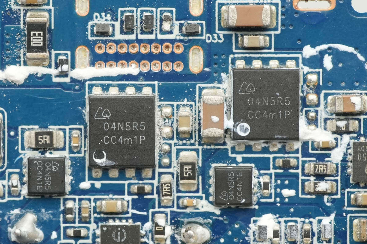
The other two buck MOSFETs have the same model and are packaged in a DFN5*6 form factor.
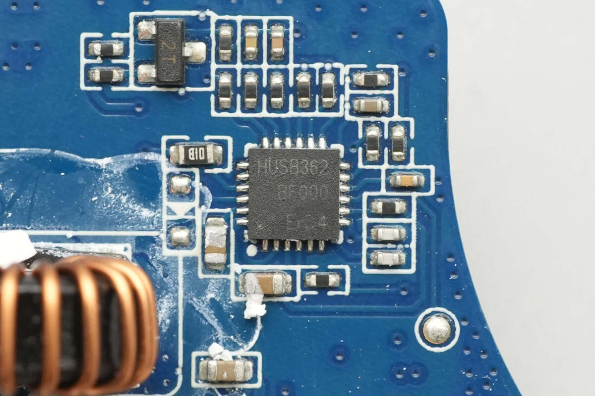
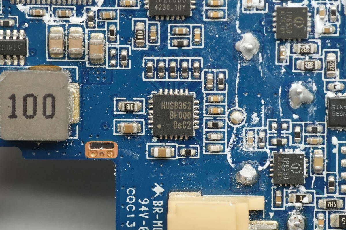
The protocol chip for the USB-C1 and USB-C2 interfaces is from Hynetek, model HUSB362. This is a high-performance PD protocol chip that supports PD3.1 EPR and integrates a 32-bit RISC-V MCU. It features 32KB of MTP memory and supports multiple PDOs with programmable voltage and current, such as PPS PDO and EPR PDO. All PDOs are fully compliant with the USB PD 3.1 V1.7 specification. The HUSB362 has passed the USB-IF Association's PD3.1 compliance testing, with an EPR TID of 9692.
The HUSB362 also includes a programmable DPDM PHY, with the D+ and D- pins configurable to support QC2.0, QC3.0, AFC, FCP, and Divider 3 modes, ensuring excellent compatibility with traditional devices. It integrates N-MOS drivers to control the connection between VIN and VBUS, offering protection to devices connected via the Type-C connector.
Additionally, its high voltage tolerance and protection for the CC1, CC2, D+, and D- pins enhance the overall reliability of the system. The chip also features extensive protection for Low Power Sources (LPS) and is packaged in a QFN4*4-24L form factor.

The HUSB362 integrates high-quality Constant Voltage (CV) and Constant Current (CC) control loops, along with an integrated feedback (FB) regulation mode. This makes it suitable for both AC-DC and DC-DC applications. The chip's dual-loop design allows users to achieve application designs with minimal external components, enhancing space utilization, simplifying the design complexity, and reducing BOM (Bill of Materials) costs.
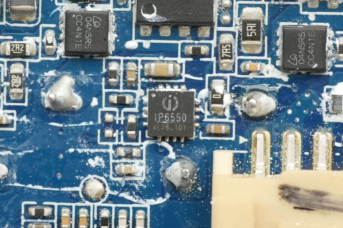
The USB-C2 port uses the Injoinic IP6550 synchronous buck controller.
The USB-C2 port uses the Hynetek HUSB362 protocol chip.

The protocol chip for the USB-C3 and USB-A interfaces is from Injoinic, model IP2736U. This is a fast charge protocol control IC that integrates multiple protocols for USB ports. The IP2736U supports various fast charging protocols, including USB Type-C DFP, PD2.0/PD3.1/PPS/EPR 28V, HVDCP QC5/4+/3+/3.0/2.0, FCP, SCP, AFC, SFCP, MTK PE+2.0/1.1, UFCS, Apple 2.4A, BC1.2, and Samsung 2.0A. It provides a complete solution for applications such as adapters, car chargers, and other unidirectional output devices.

Here is the information about Injoinic IP2736U.

The synchronous buck controller is from Injoinic, model IP6550.
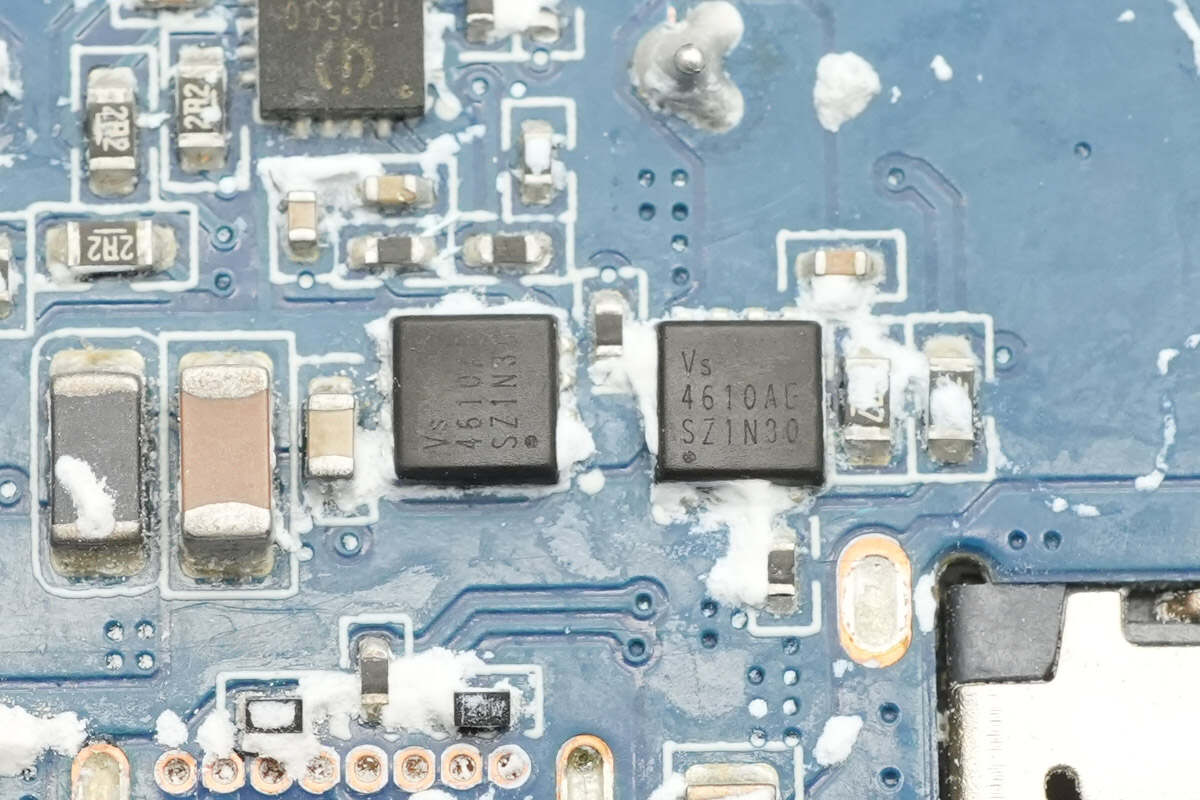
The synchronous buck MOSFETs are from Vergiga, model VS4610AE. They are NMOS transistors with a voltage rating of 40V, a Rds(on) of 6.8mΩ, and are packaged in a PDFN3333 form factor.
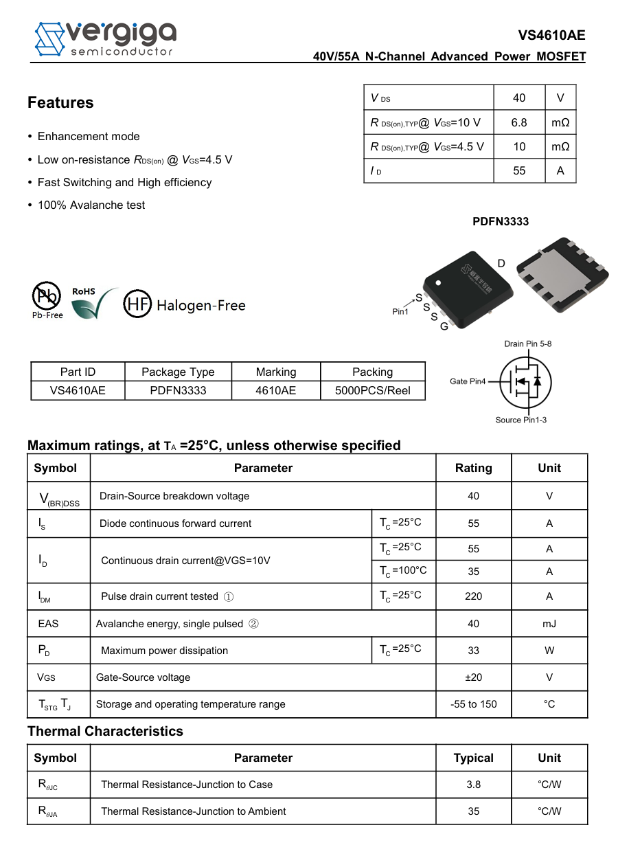
Here is the information about Vergiga VS4610AE.
The three buck inductors are wound with enameled wire.
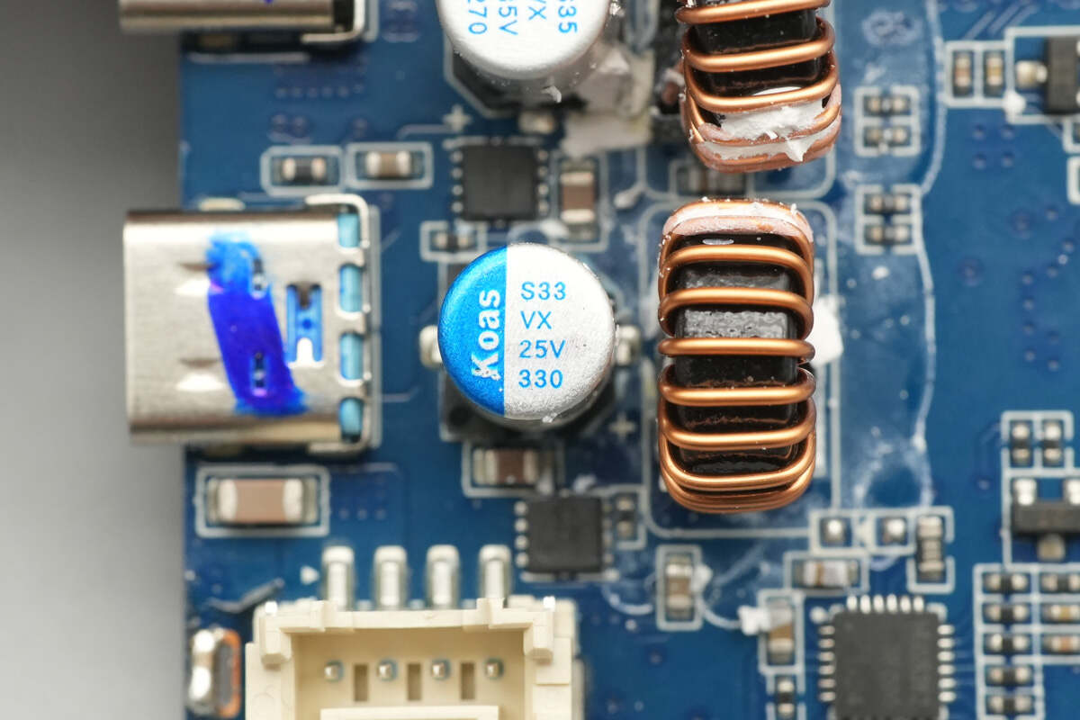
The filter capacitor used for the built-in cable is from Koshin, with a specification of 25V, 330μF.
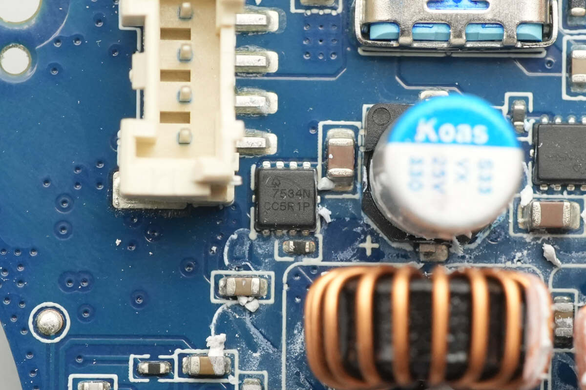
The VBUS MOSFET is from AOS, model CQY7534N. It is an NMOS transistor with a voltage rating of 30V, a Rds(on) of 4.8mΩ, and is packaged in a DFN3*3EP form factor.

The filter capacitor for the USB-C2 has a specification of 35V, 270μF.
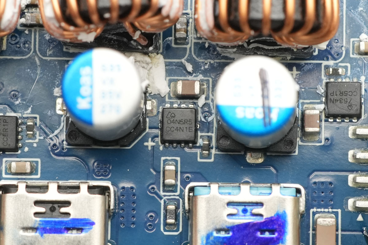
The VBUS MOSFET is from AOS, marked with 04N5R5.
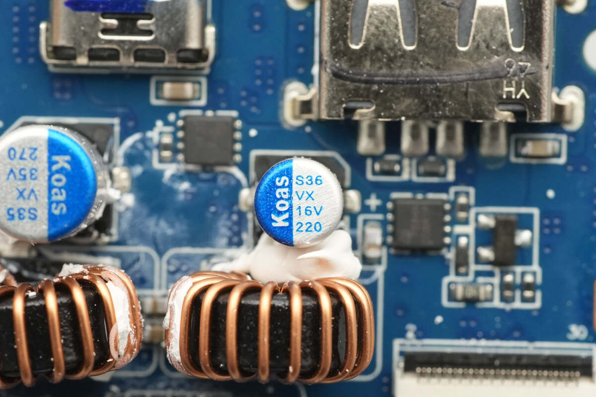
The filter capacitor for the USB-C3 and USB-A has a specification of 16V, 220μF.

The VBUS MOSFET is the AOS CQY7534N.
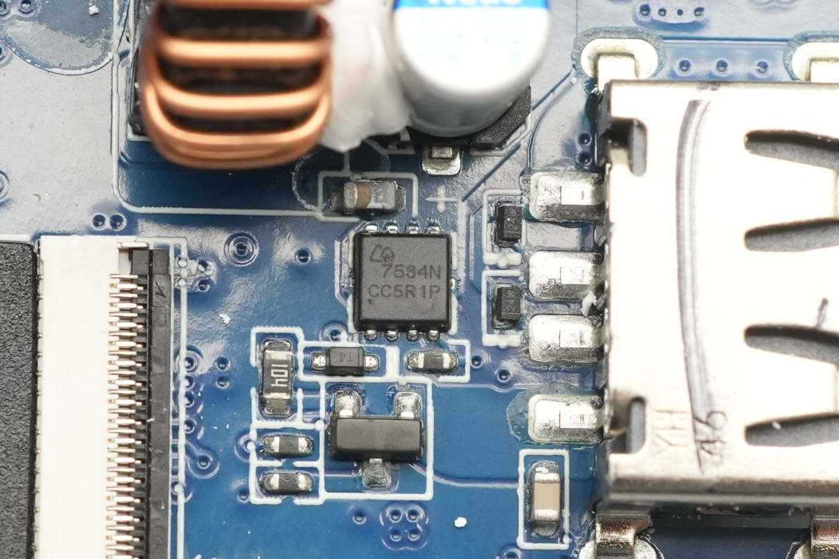
The other VBUS MOSFET has the same model.
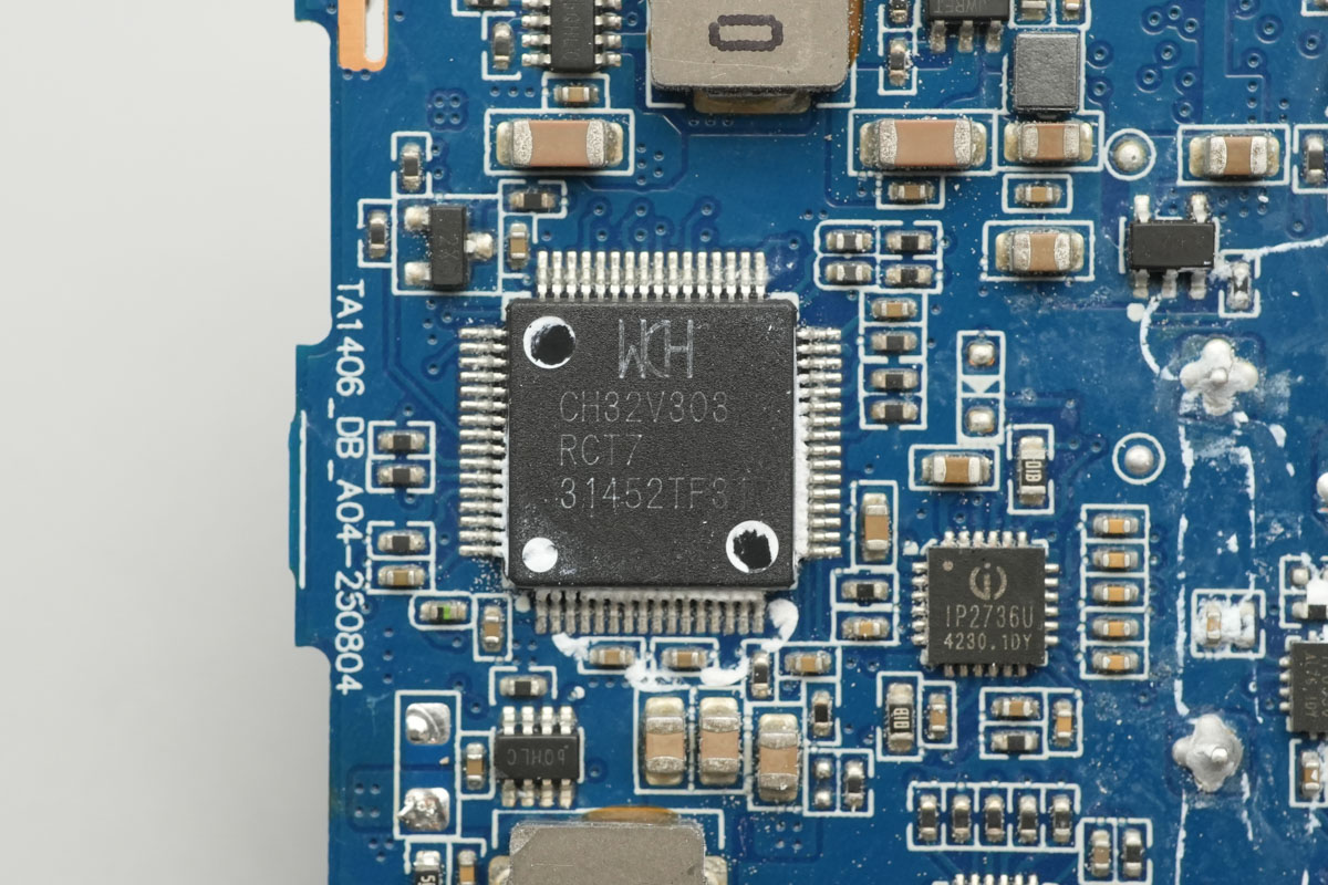
The MCU is from WCH, model CH32V303RCT7. It is an industrial-grade, general-purpose enhanced MCU based on the 32-bit RISC-V instruction set and architecture. It features 64K SRAM and 256K Flash memory, with a clock speed of 144MHz. The MCU also supports interfaces such as I2C, I2S, SPI, USART, SDIO, and a CAN controller. It is packaged in an LQFP64M form factor.

The synchronous buck converter chip is from JOULWATT, marked with JWRE, model JW5018X. It is a synchronous buck regulator with an input voltage range of 4.5V to 42V, a switching frequency of 1.1MHz, and an output current of 600mA. The chip features short-circuit protection, over-temperature protection, and a low-dropout mode. It is packaged in an SOT23-6 form factor.
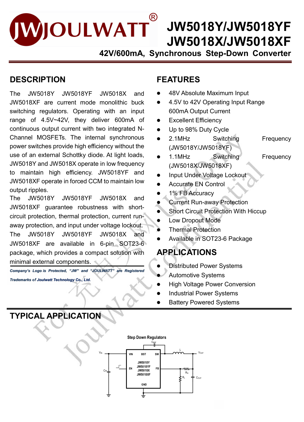
Here is the information about JOULWATT JW5018.

Close-up of the buck inductor.

The voltage regulator chip is from 3PEAK, marked with L7J, model TPL720F33. It supports a 6V input voltage, with a 3.3V output and a maximum output current of 400mA. The chip features current limiting and overcurrent protection. It is packaged in an SOT23-5 form factor.

The synchronous buck chip is from Silergy, marked with bQ, model SY8303A. It supports an input voltage range of 4.5V to 40V, with a selectable switching frequency. The chip is capable of providing up to 3A of output current and features cycle-by-cycle peak current limiting, short-circuit protection, and over-temperature shutdown. It is packaged in a TSOT23-8 form factor.
Close-up of the 10μH alloy inductor.
The other synchronous buck chip is also the Silergy SY8303A.
Close-up of the 10μH alloy inductor.

Close-up of the chip marked with 22588.

The Schottky diodes are marked with SS34L.
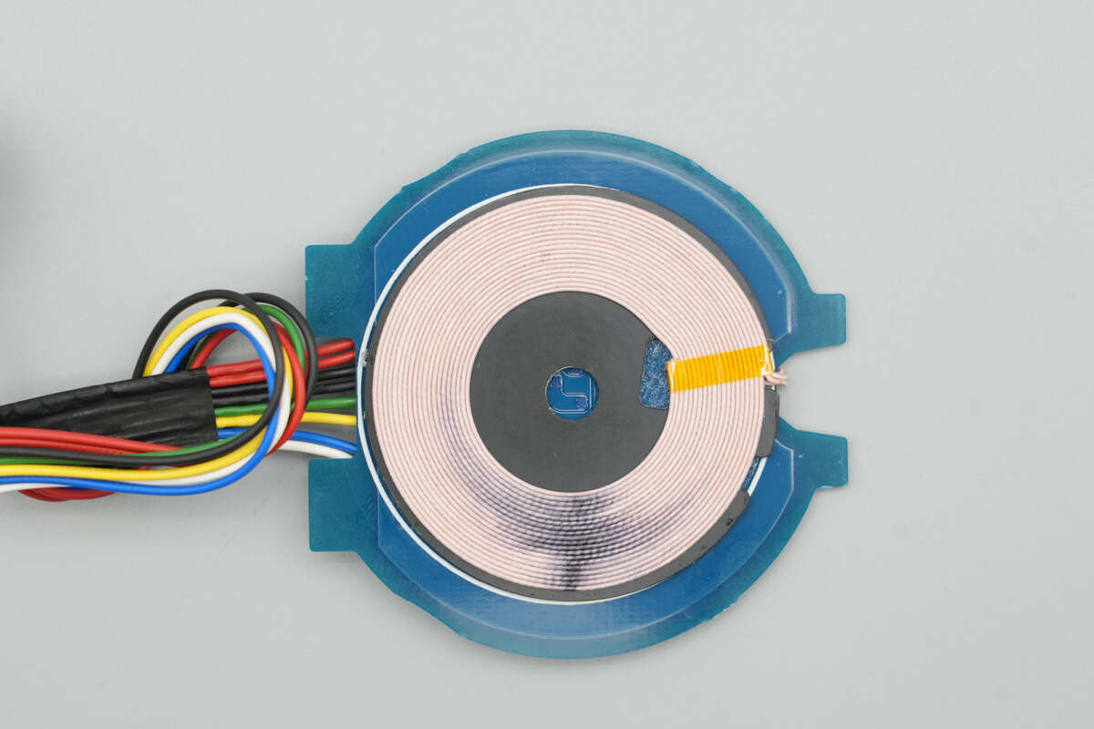
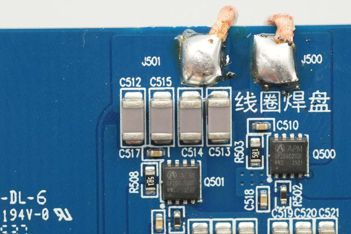
The front of the magnetic wireless charging module features a charging coil and a magnetic shielding plate.
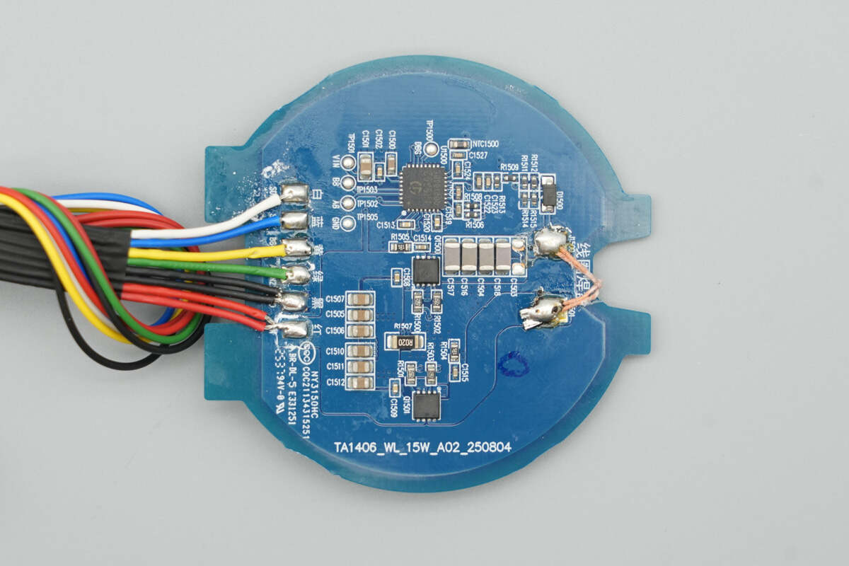
The back contains the wireless charging master control chip, the wireless charging power MOSFETs, capacitors, and resonant capacitors.
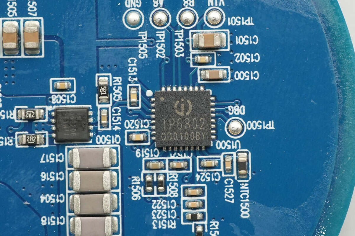
The wireless charging master control chip is from Injoinic, model IP6802. It is a complete single-chip wireless charging SoC. This chip integrates the PD3.0 protocol, supporting both PD fast charging and DP&DM fast charging power supply, with the ability to automatically request fast charging voltage. It supports an input voltage range of 4V to 20V. The chip features an internal full-bridge driver and digital demodulation, eliminating the need for external drivers and operational amplifiers. With four MOSFETs and a small number of external components, it can deliver a complete Qi2 wireless charging solution. The chip is packaged in a QFN32 form factor.

Here is the information about Injoinic IP6802.

Six MLCC capacitors are connected in parallel.

The wireless charging power MOSFET is from Vergiga, model VS3622DE. It is a dual NMOS transistor with a voltage rating of 30V and a R_DS(on) of 10mΩ. It supports 5V logic voltage drive and is packaged in a PDFN3333 form factor.
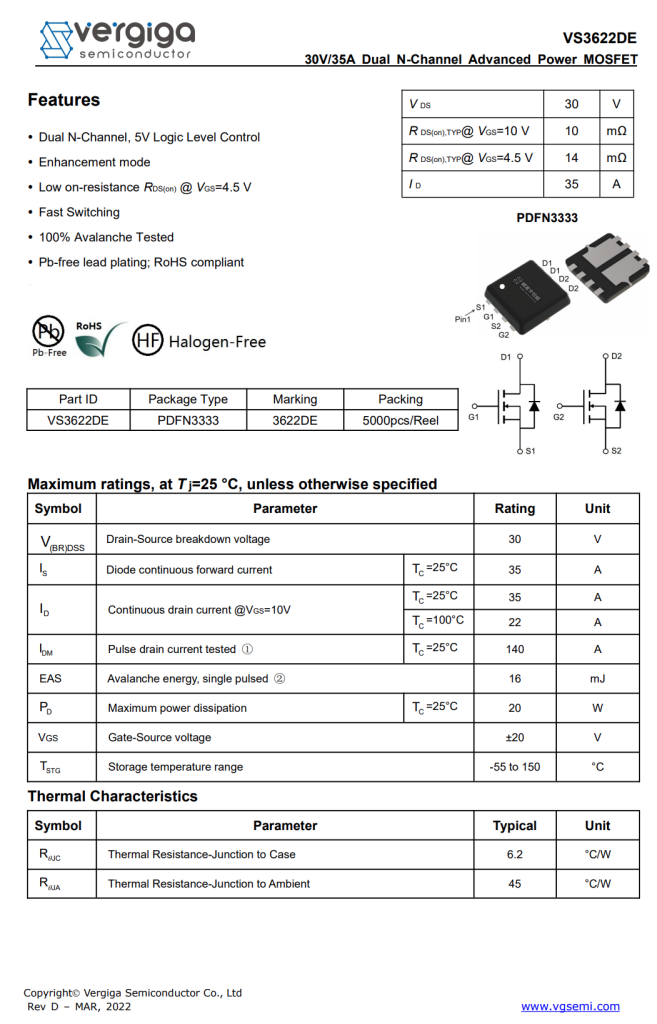
Here is the information about Vergiga VS3622DE.
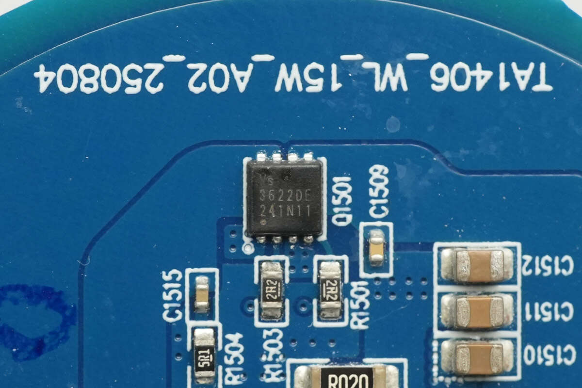
The other wireless charging power MOSFET is of the same model.

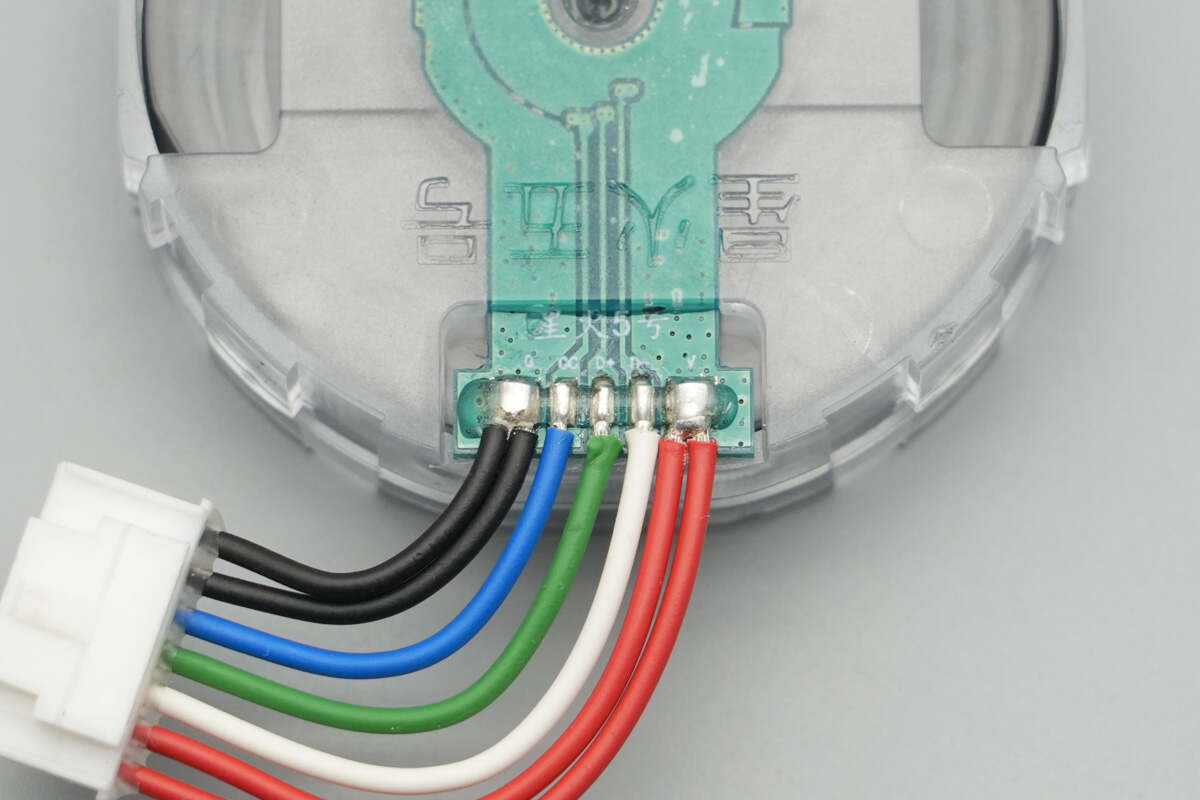
The connecting wires are connected by soldering.

The front of the wireless charging module features a charging coil and a magnetic shielding plate.
The back of the wireless charging module contains the wireless charging master control chip, wireless charging power MOSFETs, and resonant capacitors.
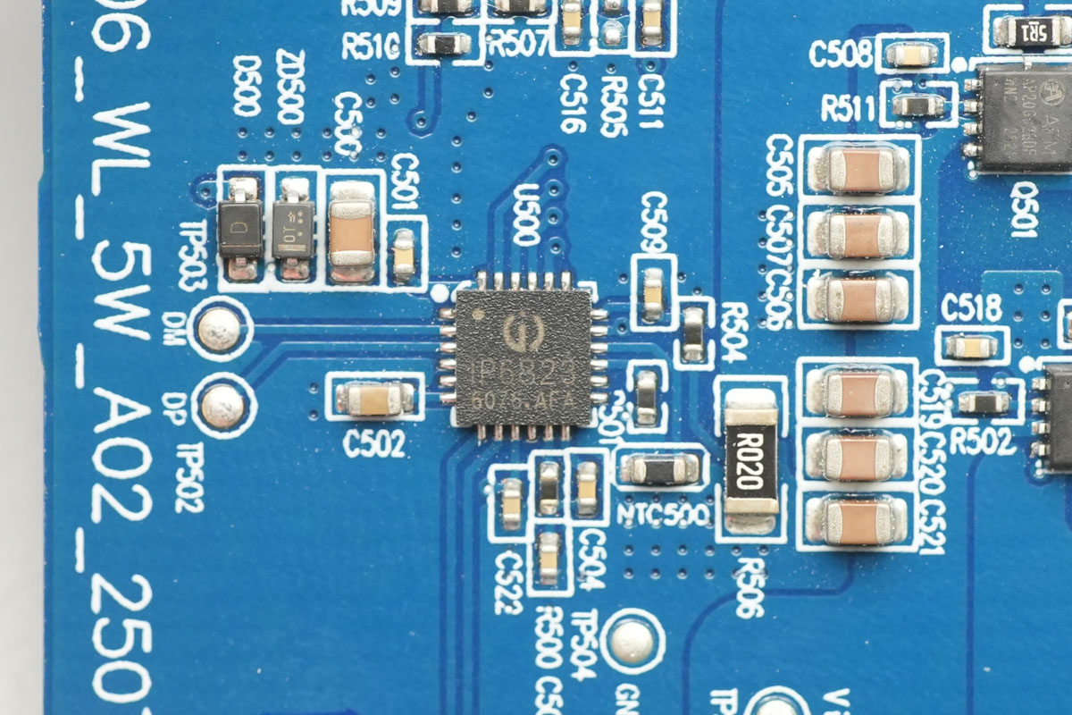
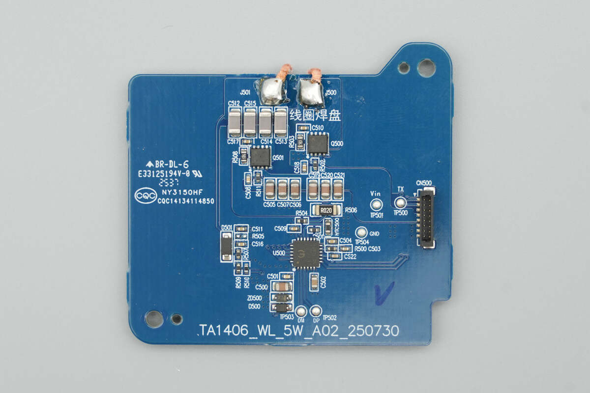
The wireless charging master control chip is from Injoinic, model IP6823. It is a highly integrated wireless charging transmitter control chip that complies with the WPC Qi standard. The chip internally integrates an H-bridge drive module, ASK communication demodulation module, and necessary resources for the adapter fast-charging sink protocol.
The IP6823 supports functions such as protocol handling, foreign object detection sensitivity, and customizable indicator lights. It comes in a QFN24 package with a pin layout optimized for wireless charging applications, making it very convenient for PCB design in wireless charging solutions.
Here is the information about Injoinic IP6823.

The wireless charging power MOSFETs are from APM, model AP20G02BDF. This is a dual N+P MOSFET suitable for wireless charging full-bridge applications. The NMOS has a voltage rating of 20V with a Rds(on) of 12mΩ, while the PMOS has a voltage rating of -20V with a Rds(on) of 25mΩ. These MOSFETs come in a PDFN3*3-8L package.
Close-up of four NPOresonant capacitors connected in parallel.
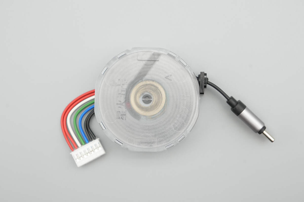
The retractable cable module uses a transparent plastic housing.
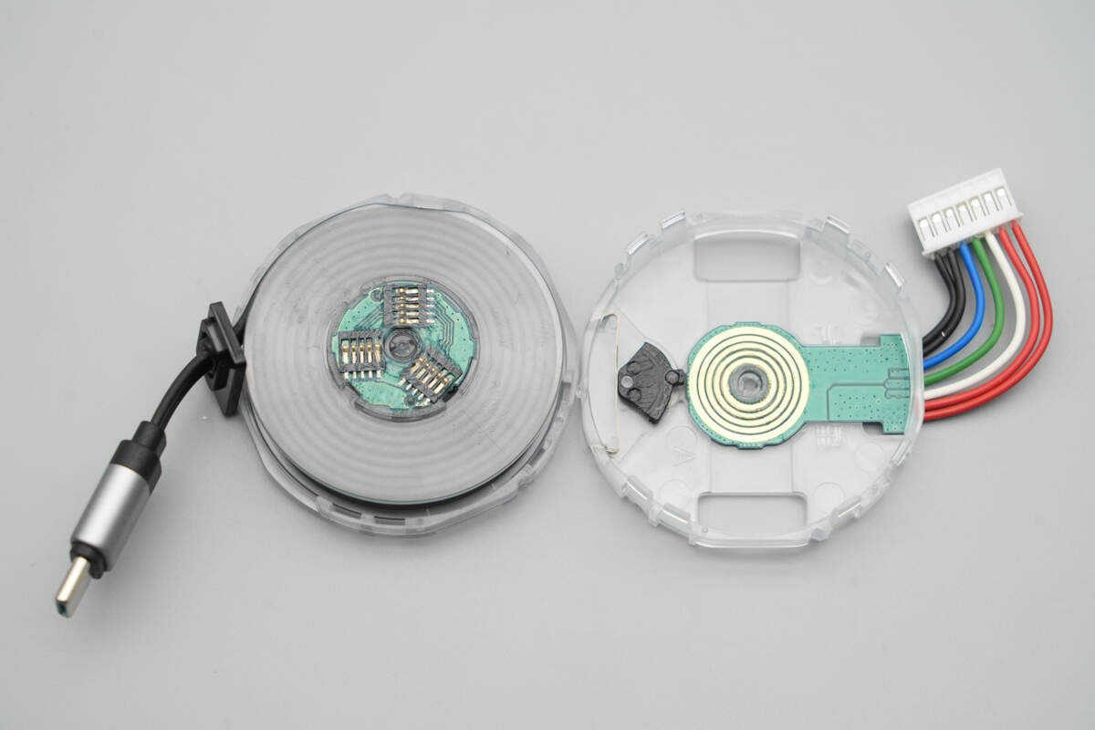
Upon opening the housing, the module features a brush and PCB slip ring inside.
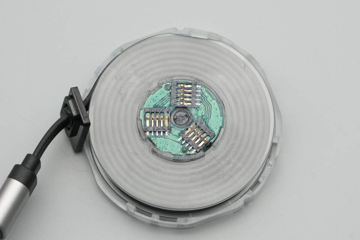
The brush is soldered onto the circular PCB.
Close-up of the PCB slip ring.
The wire solder joints are reinforced with glue.
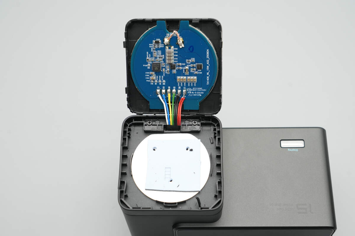
Finally, remove the display panel.
Inside, there is an LCD screen and a light strip.

On the right side of the light strip, there is a light filter.
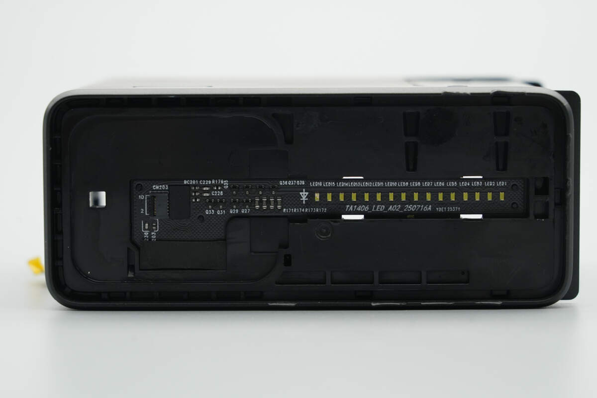
After removing the light filter, inside there is a long strip PCB soldered with 16 LED light beads.
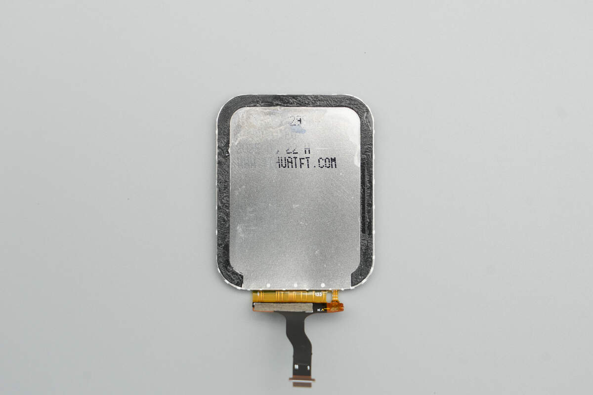
The back of the screen is covered with a metal shell, which is secured in place with double-sided adhesive.

The interior of the magnetic wireless charging panel contains magnets and double-sided adhesive.
The back of the shell is equipped with a thermal pad and a heat dissipation aluminum plate.

Well, those are all components of the CUKTECH 15 Charging Station.
Summary of ChargerLAB

Here is the component list of the CUKTECH 15 Charging Station for your convenience.
It is equipped with a USB-C built-in cable, two USB-C ports, and one USB-A port, along with two wireless charging panels. It can simultaneously charge a laptop, smartphone, and earbuds. The built-in cable supports up to 120W output power, while the USB-C ports support up to 140W output power. The screen displays the power output of each port.
After taking it apart, we found that the PCBA module consists of multiple small PCBs connected by wires. It uses a PFC+LLC+Synchronous Rectification architecture. The MPS CD1271 master control chip is used for both PFC and LLC control, while the MP6925 is used for synchronous rectification.
The PFC uses Innoscience INN700D190B GaN FET, paired with Jingdao Microelectronics ES5JCC rectifier. The LLC MOSFETs use HWDZ MS65R360. The secondary buck output is controlled by Injoinic IP6550 synchronous buck controllers. The USB-C cable and USB-C2 port use Hynetek HUSB362 protocol chips, while the USB-C3 and USB-A ports use an Injoinic IP2736U protocol chip.
The two wireless charging modules use Injoinic IP6802 and IP6823 master control chips. The PCBA module is attached with thermal pads and coated with thermal adhesive, with copper sheets on the outer side. Inside, the high-voltage filter capacitors and solid capacitors are from Koshin, while TRX SMD Y capacitors are used. The overall build quality and materials are solid and reliable.
Related Articles:
1. Teardown of Xiaomi 45W GaN Pudding Charger (MDY-18-EZ)
2. Teardown of Anker Nano 45W GaN Charger with Display (A121D)
3. Teardown of Segotep 3200W Titanium-Rated SiC Digital Server Power Supply (CRPS3200W-12V)