Introduction
CalDigit is a well-established American brand known for its high-quality accessories, including docking stations, storage devices, and cables. Their products typically feature aluminum alloy enclosures, which provide excellent heat dissipation, strong structural integrity, and a premium look and feel. With comprehensive functionality and a wide range of ports, CalDigit has become synonymous with high-end docking solutions.
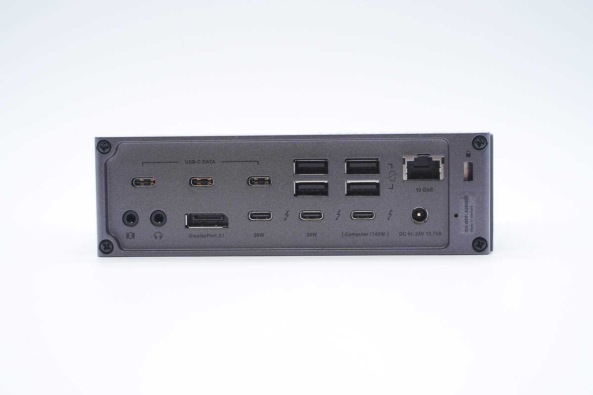
We recently got our hands on CalDigit’s TS5 Plus Thunderbolt 5 Dock. This dock features an aluminum alloy chassis and is powered by a 330W external power supply. On the front panel, it offers USB-C and USB-A ports, TF and SD card readers, and a 3.5mm audio jack. The rear panel includes Thunderbolt 5 ports, a DisplayPort 2.1, a 10Gb Ethernet port, additional USB-C and USB-A ports, and an audio interface.
The Thunderbolt 5 upstream port supports 140W PD 3.1 fast charging, while the Thunderbolt 5 downstream port and front USB-C port each deliver 36W fast charging, allowing multiple devices to be charged simultaneously.
Next, we’ll take a closer look inside the CalDigit TS5 Plus Thunderbolt 5 Dock to explore its internal design and build quality.
Product Appearance
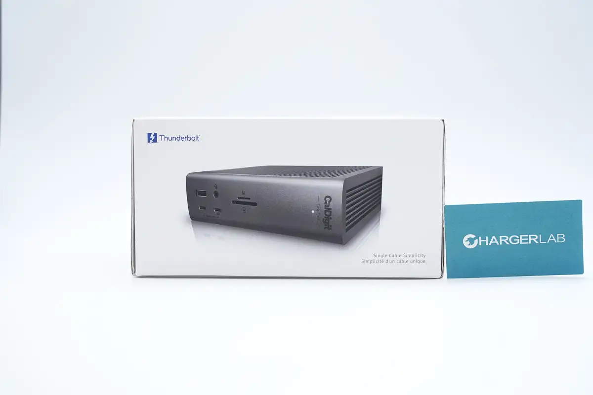
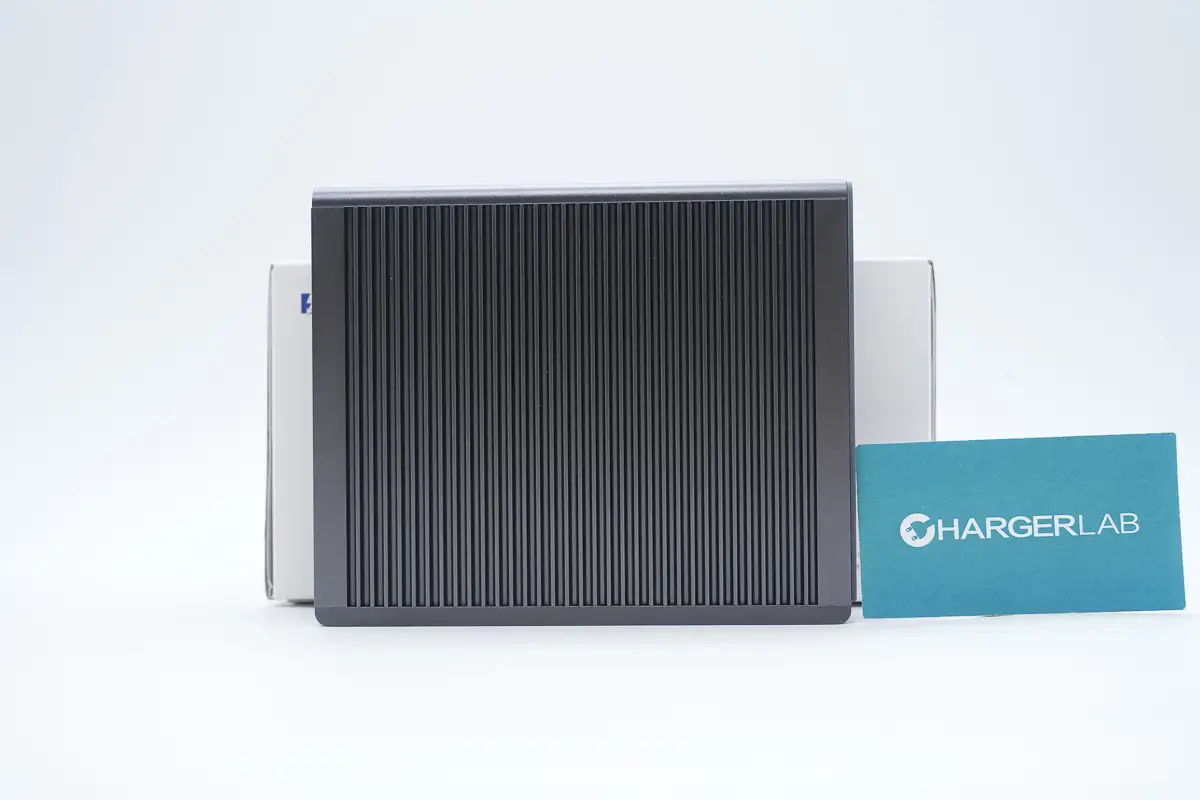
The front of the packaging box features an image of the front panel of the dock.

The top of the box is printed with the CalDigit logo, TS5 Plus, and key features.
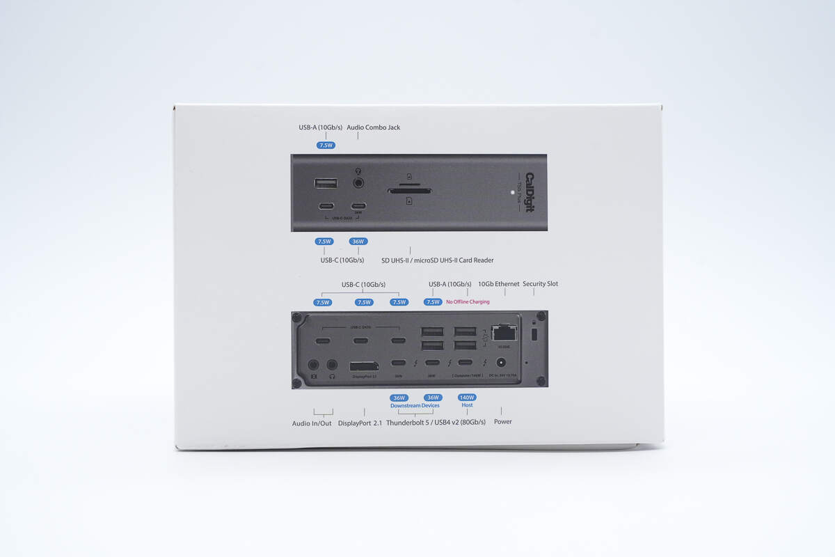
The side of the packaging box lists the port names, transfer speeds, and output power.
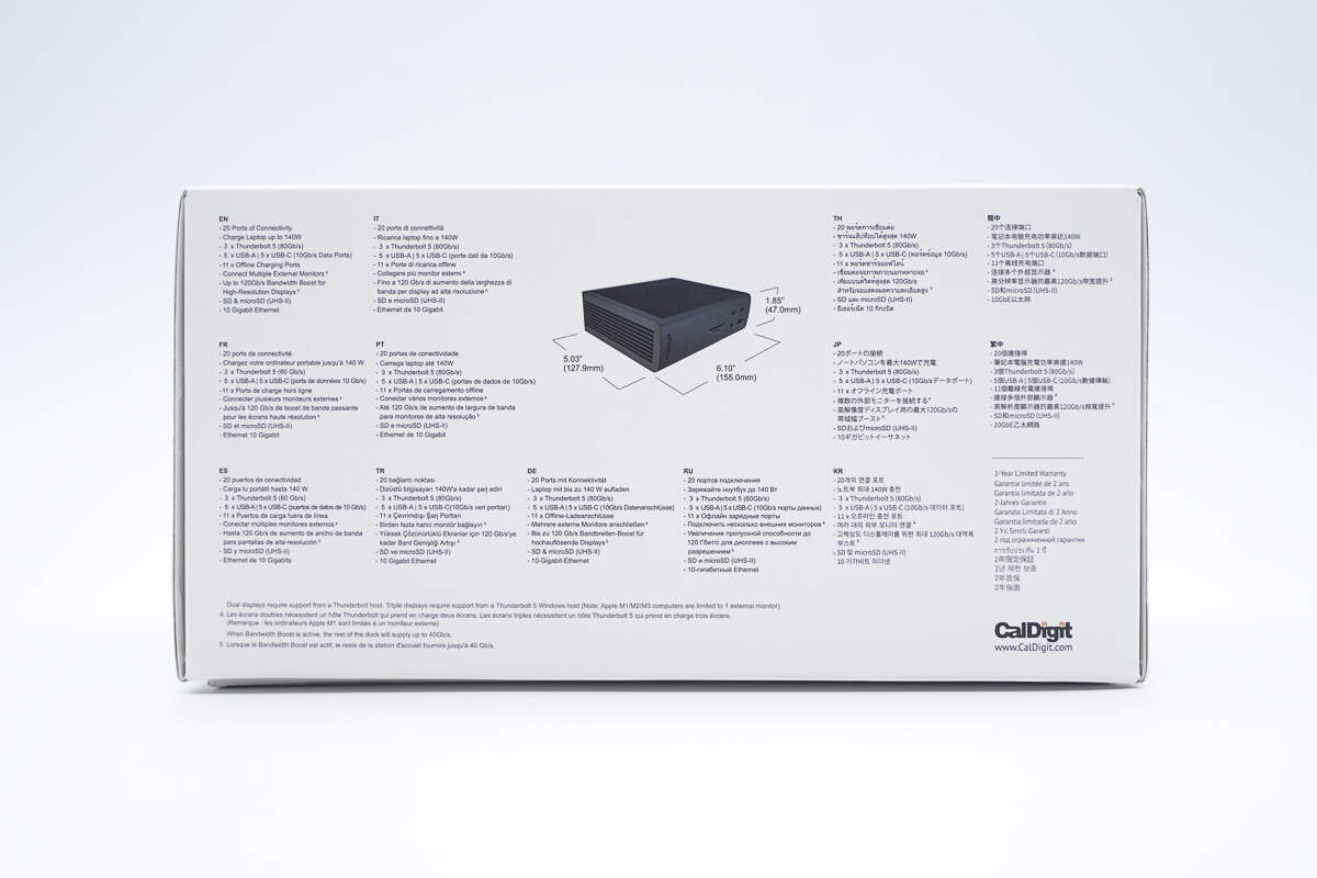
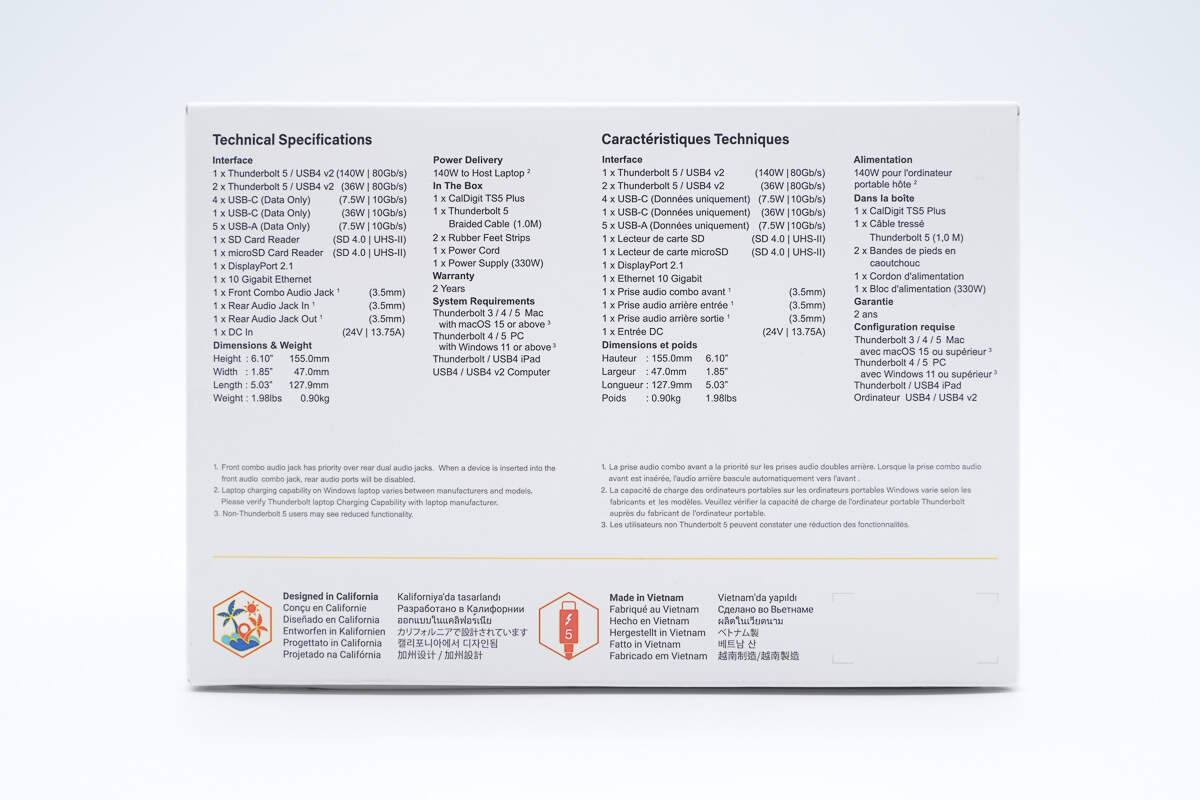
The back of the packaging box displays the dock’s dimensions along with product descriptions in multiple languages.
The side of the packaging box lists the dock’s port names and included accessories.
Take the dock out of the packaging box.
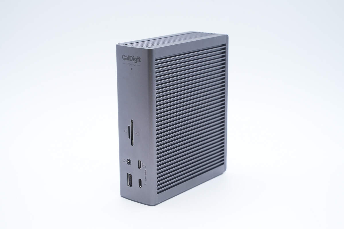
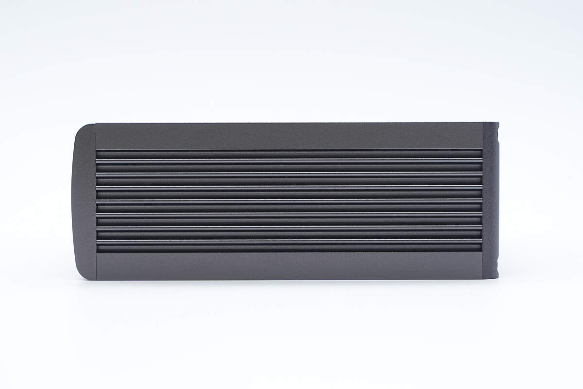
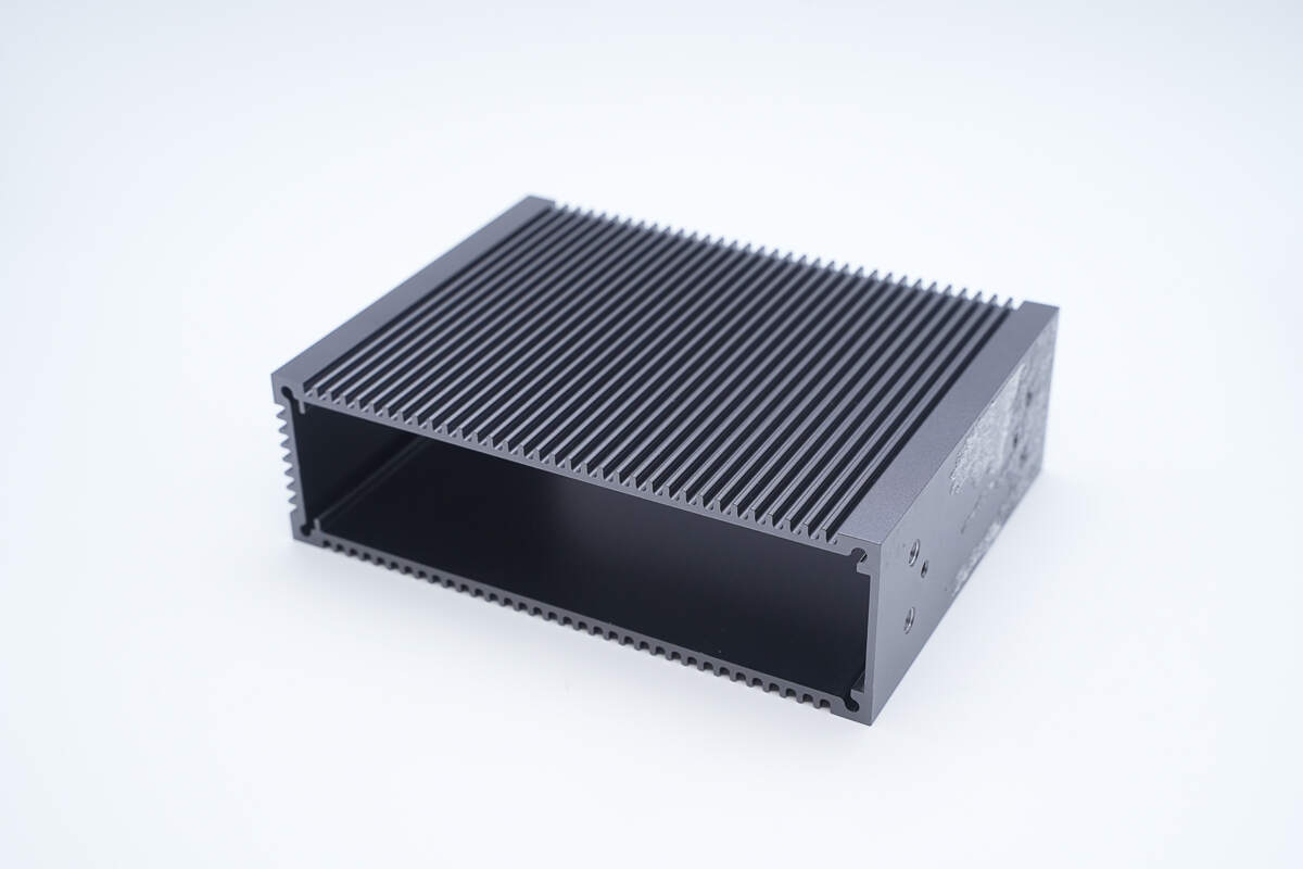
It features a black aluminum alloy enclosure.
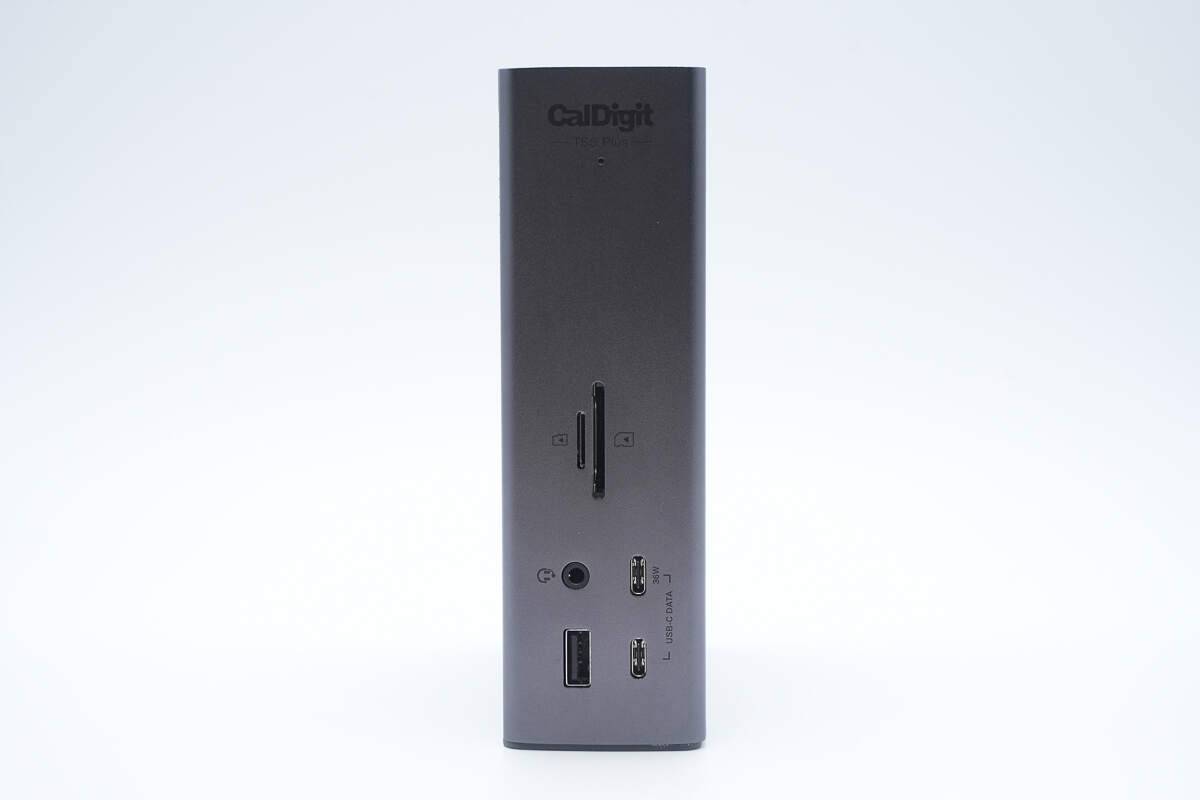
The front panel has indicator lights at the top, with TF/SD card slots, USB-C and USB-A ports, and a 3.5mm audio jack located below.
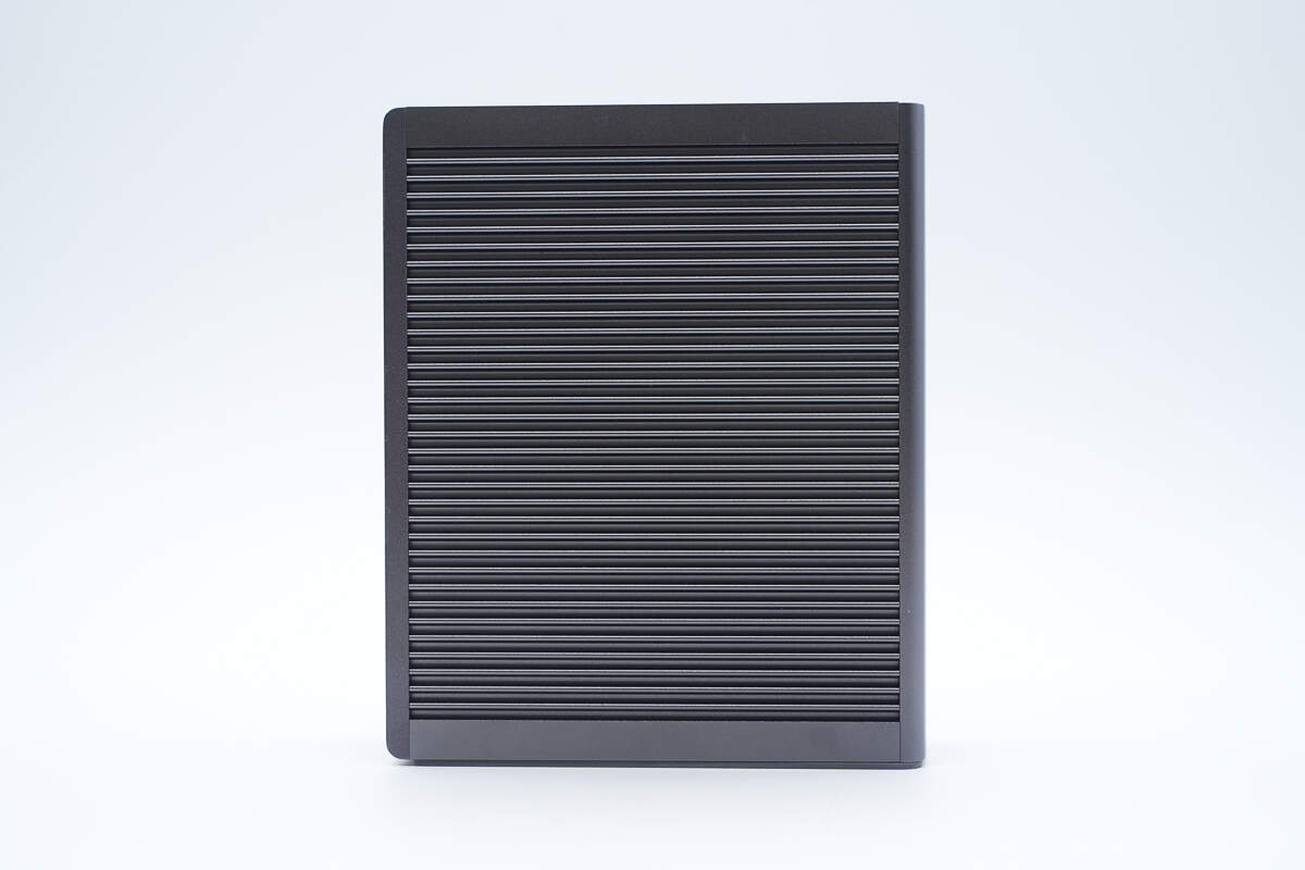
The side features a grille to increase the heat dissipation area.
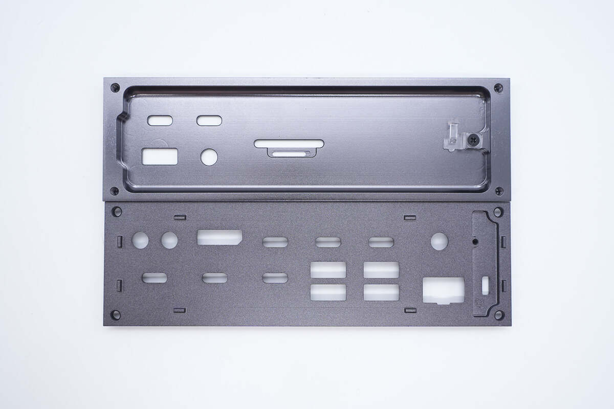
The rear panel has mounting screws located at all four corners.
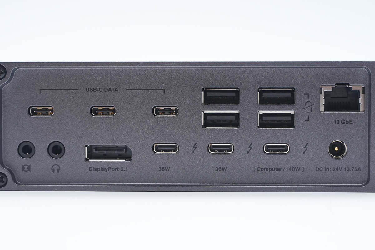
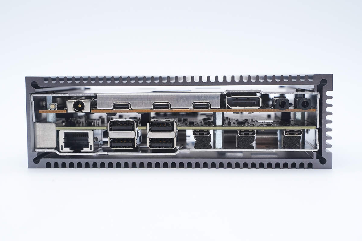
The rear panel includes three USB-C ports, four USB-A ports, a 10Gb Ethernet port, 3.5mm audio input and output jacks, a DisplayPort 2.1, three Thunderbolt 5 ports, and a power input.
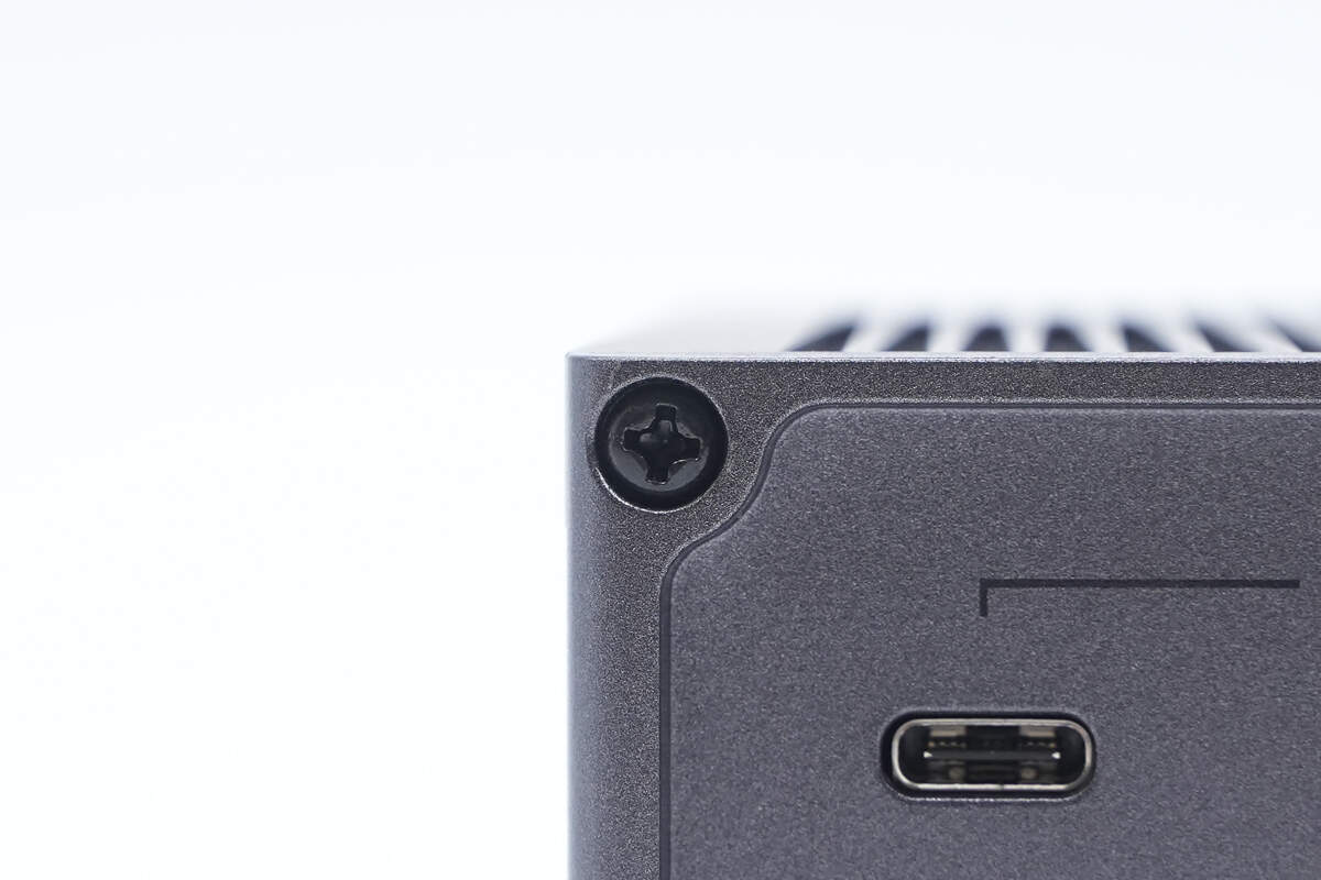
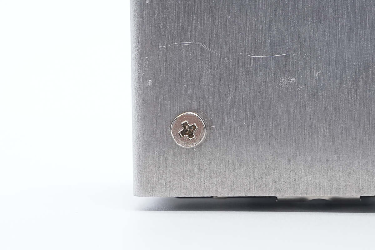
Close-up of the fixing screw.
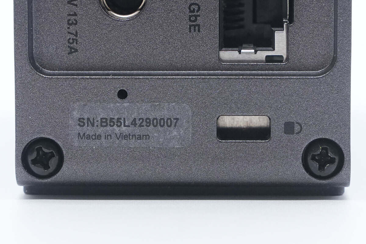
The top of the device features a security lock slot and a serial number label, indicating it is made in Vietnam.
The top also features a grille design.
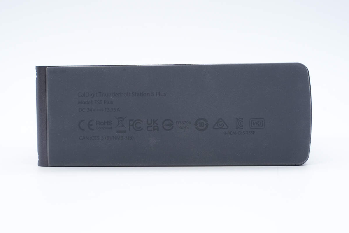
The bottom has anti-slip rubber feet with printed technical specifications.
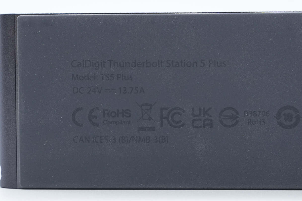
CalDigit Thunderbolt Station 5 Plus
Model: TS5 Plus
DC 24V 13.75A
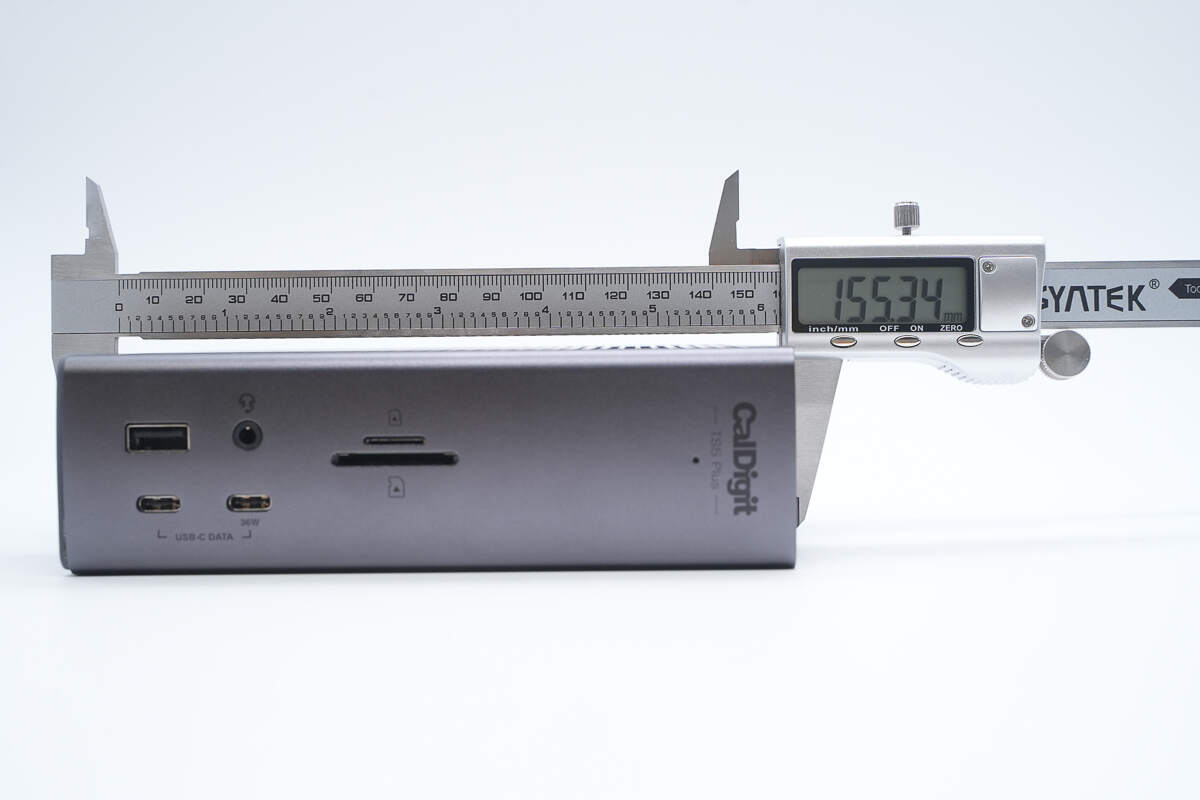
The length is about 155.3 mm (6.11 inches).
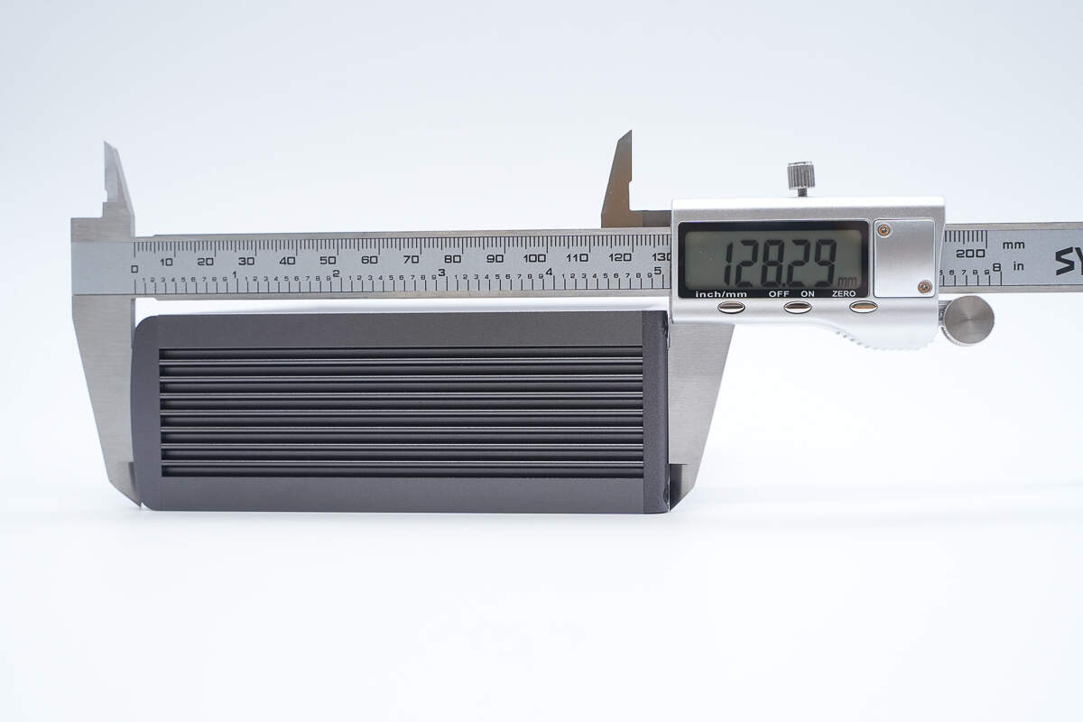
The width is about 128.3 mm (5.051 inches).
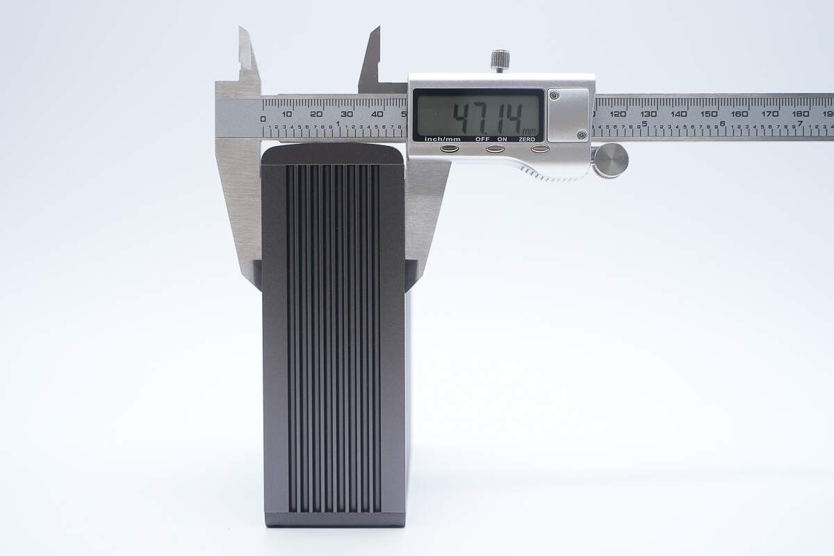
The thickness is about 47.1 mm (1.85 inches).
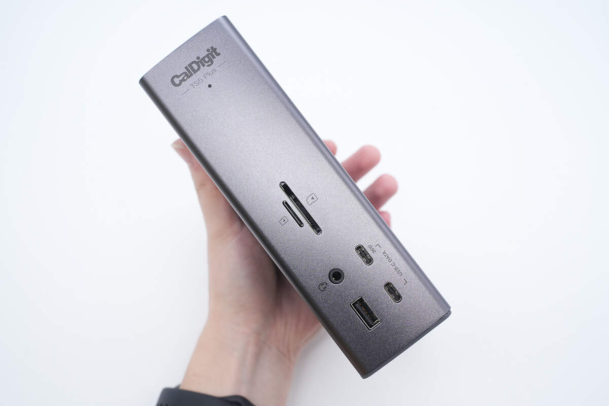
That's how big it is in the hand.

The weight is about 890 g (31.39 oz).
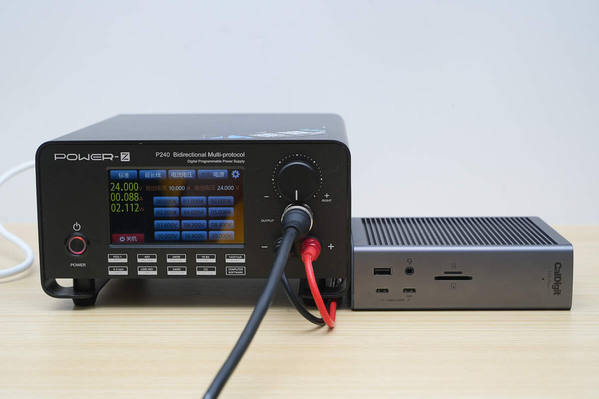
The dock is powered using the POWER-Z P240 multi-protocol bidirectional power meter.
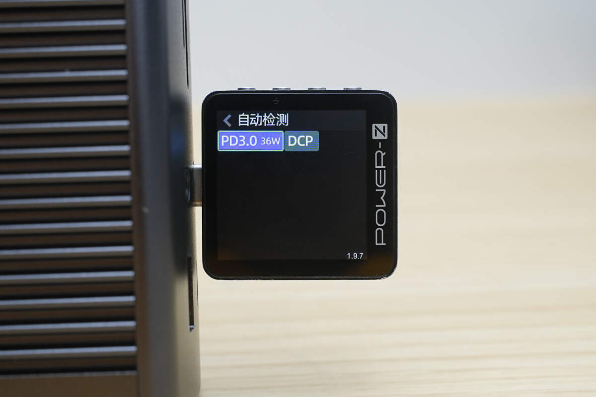
ChargerLAB POWER-Z KM003C shows that the USB-C port supports PD3.0 and DCP charging protocols.
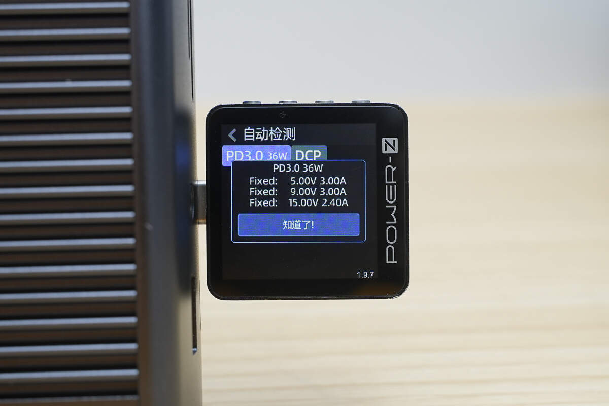
And it has three fixed PDOs of 5V3A, 9V3A, and 15V2.4A.
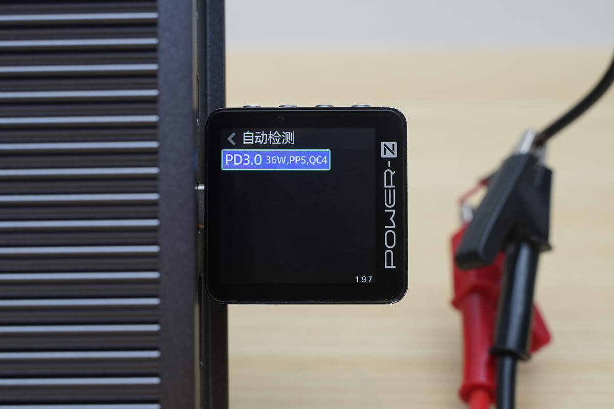
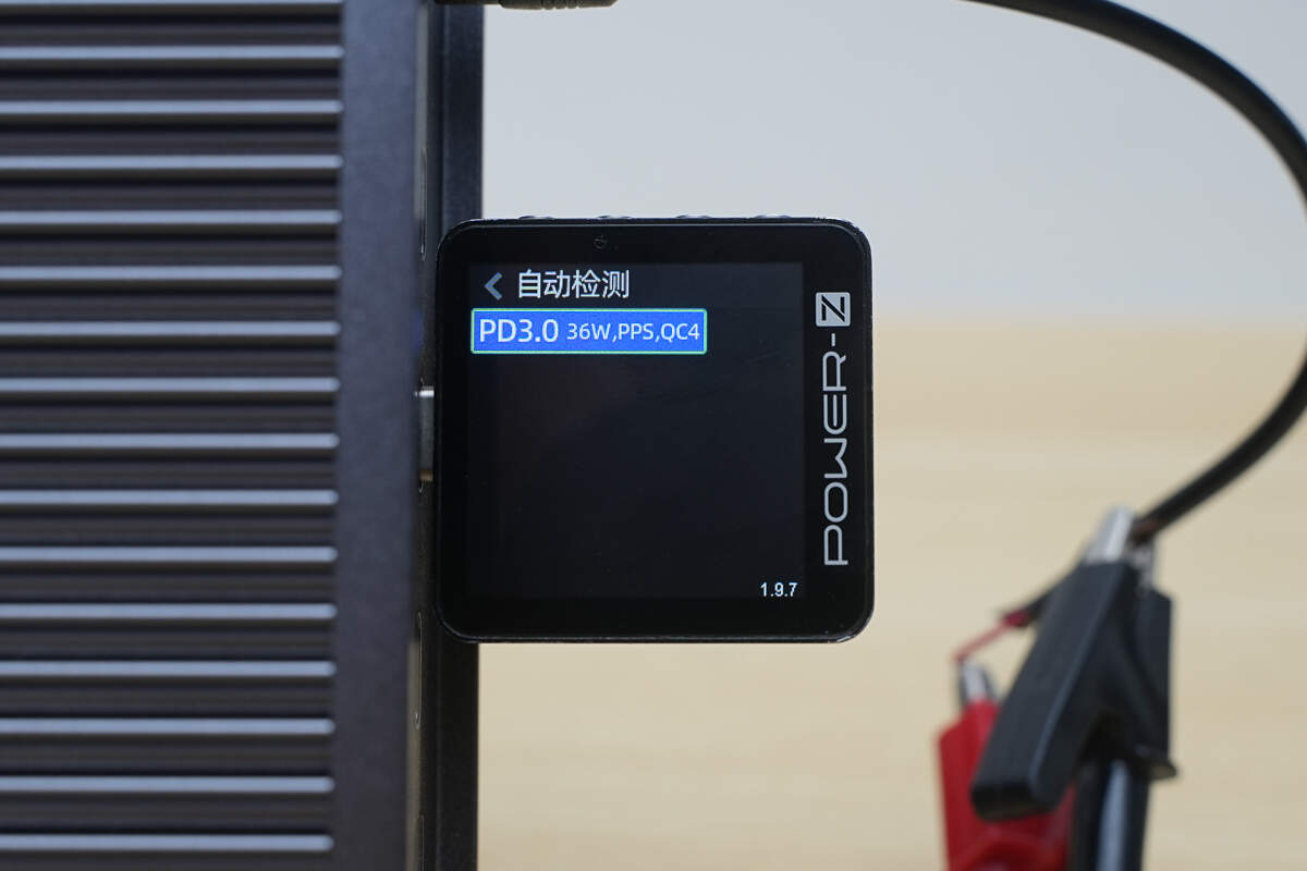
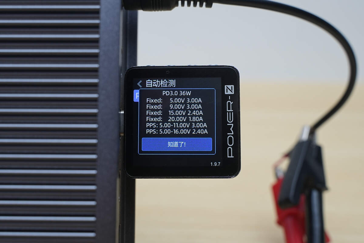
ChargerLAB POWER-Z KM003C shows that the Thunderbolt 5 downstream port supports PD 3.0, PPS, and QC4 charging protocols.
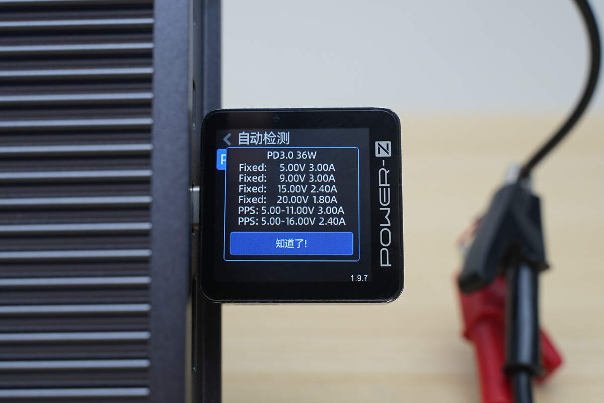
And it has four fixed PDOs of 5V3A, 9V3A, 15V2.4A, and 20V1.8A. It also has two sets of PPS, which are 5-11V3A and 5-16V2.4A.
The other Thunderbolt 5 downstream port supports the same charging protocols.
The PDO messages are also identical.
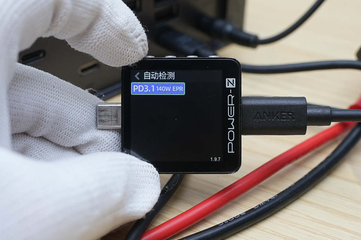
The Thunderbolt 5 upstream port supports PD 3.1 with 140W charging capability.
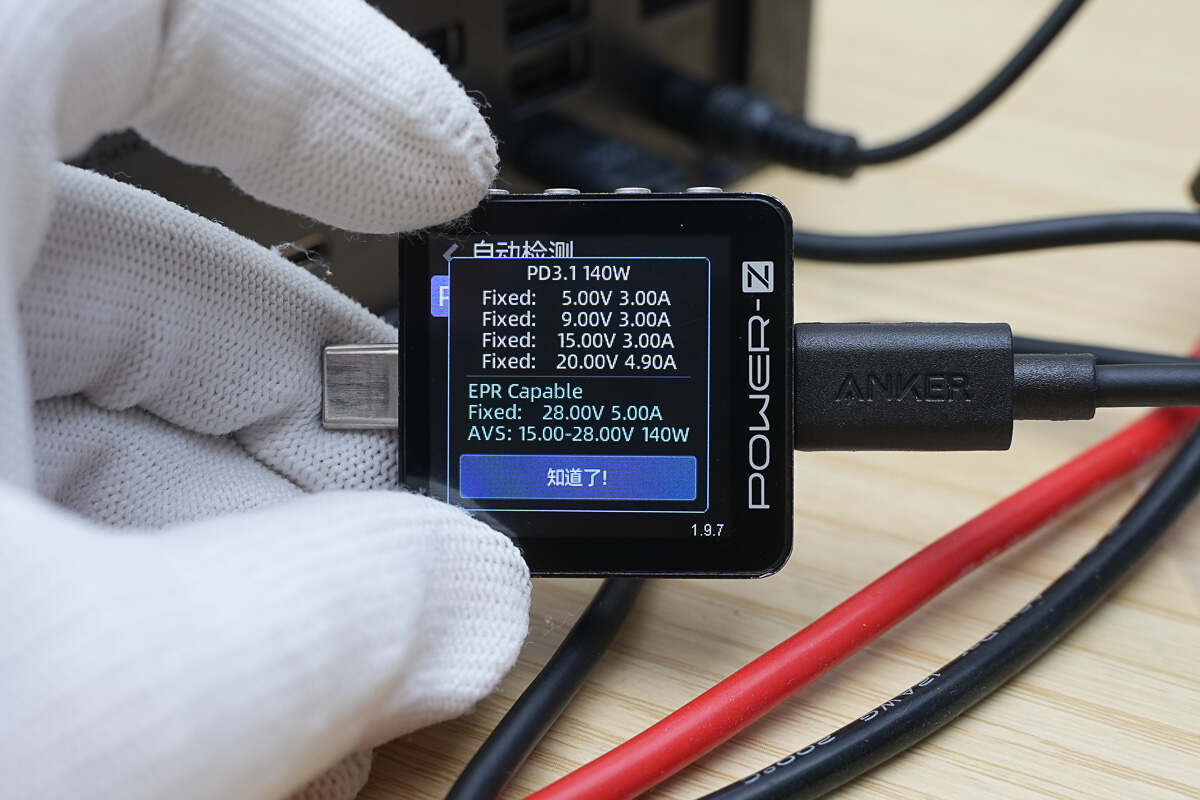
And it has five fixed PDOs of 5V3A, 9V3A, 15V3A, 20V4.9A, and 28V5A. It also has one set of AVS, which is 15-28V 140W.
Teardown
Next, let's take it apart to see its internal components and structure.
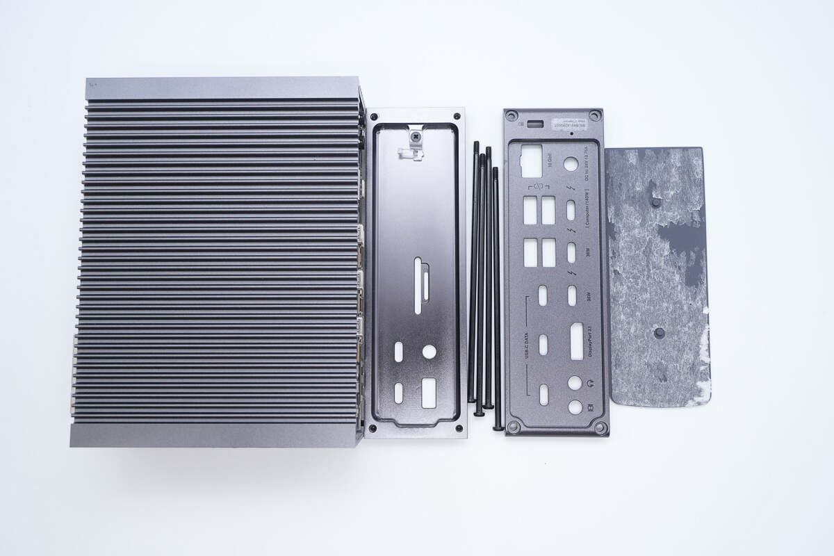
Unscrew the screws, peel off the rubber pads on the bottom, and remove the side panels.
The side panels are made using CNC machining.
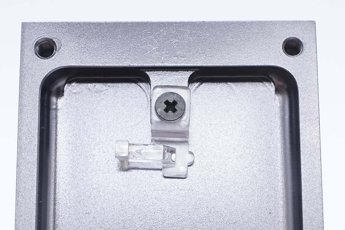
The light guide for the indicator is secured with screws.
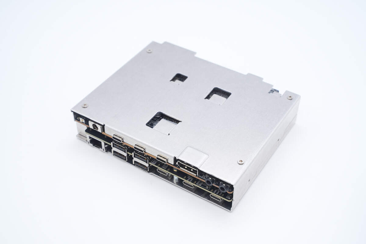
The dock’s core is equipped with an aluminum alloy shielding cover. The PCBA modules are secured to the shielding cover using standoffs.
The opposite side features the same design.
The anti-slip rubber feet are secured using double-sided adhesive.
There are screws located on the bottom of the device.
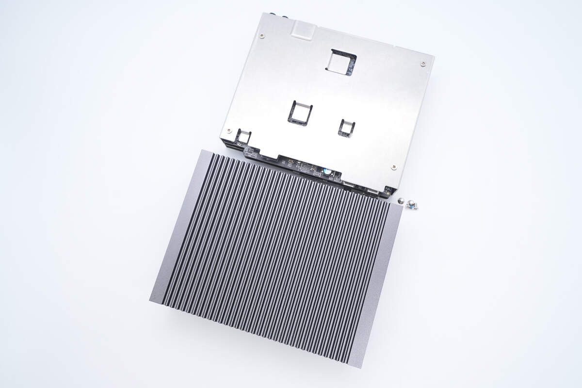
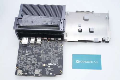
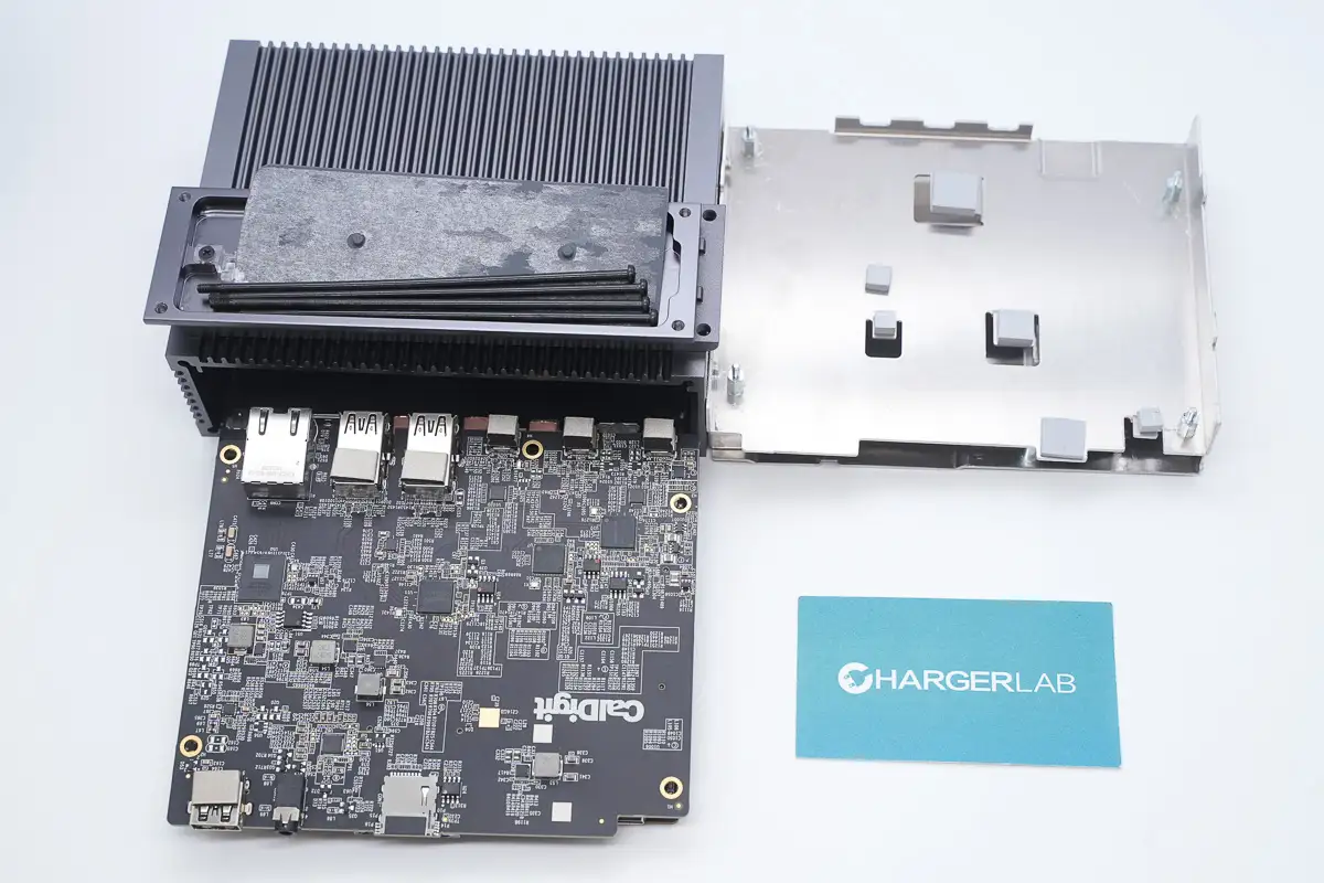
Remove the dock’s internal assembly from the enclosure.
An overview of the aluminum alloy dock enclosure.
The aluminum alloy shielding cover is secured with screws.
The other side features the same design as well.
Unscrew the remaining screws to continue the disassembly.
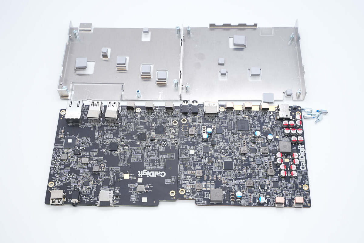
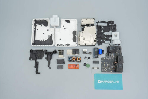
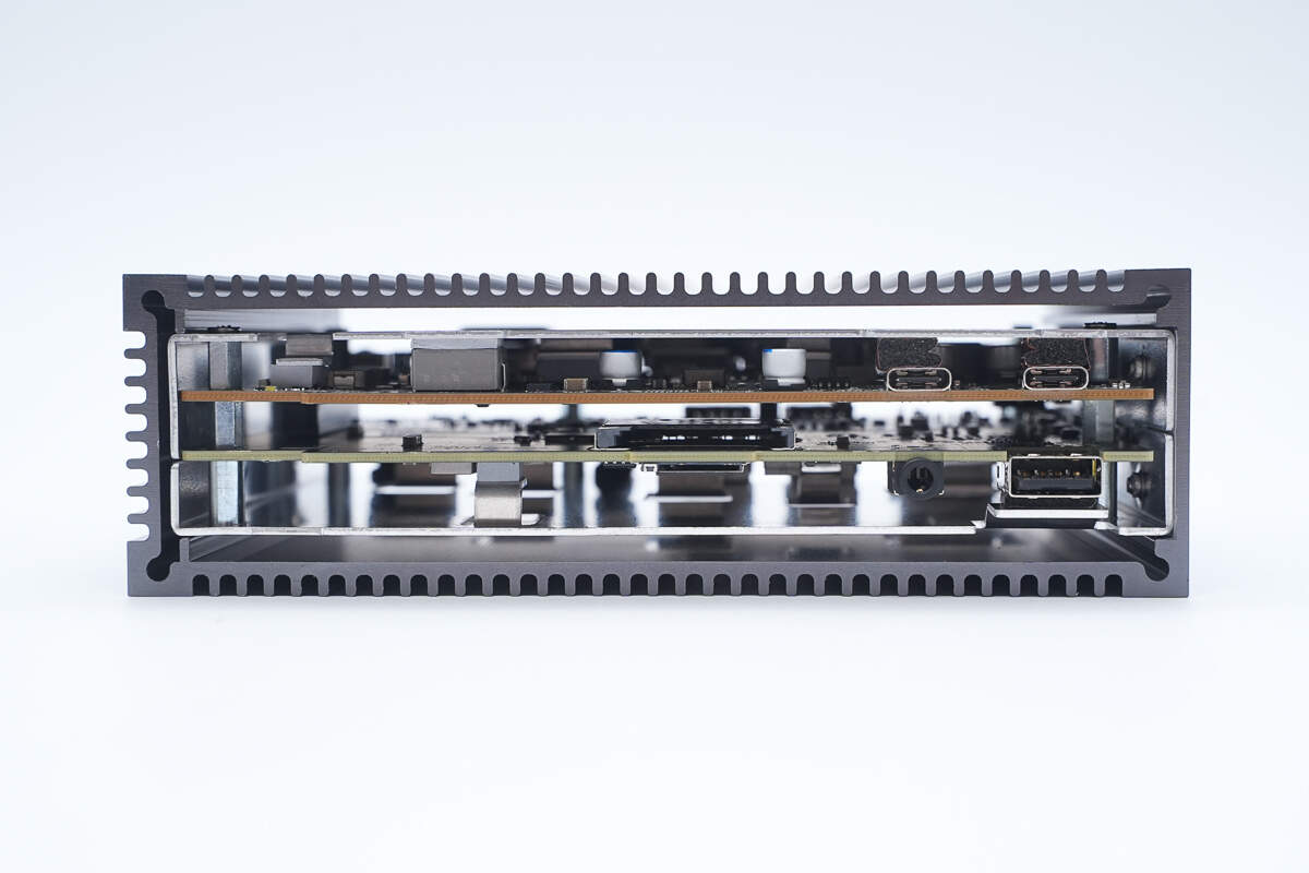
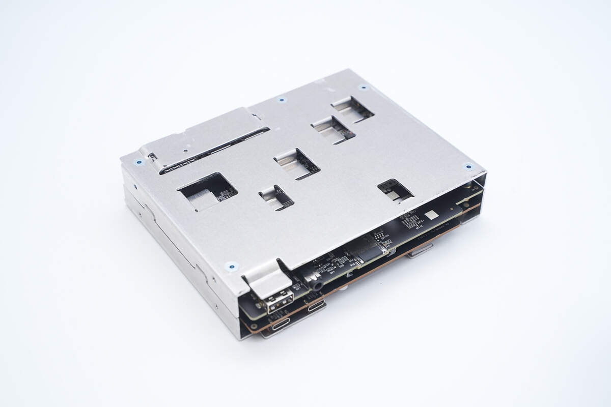
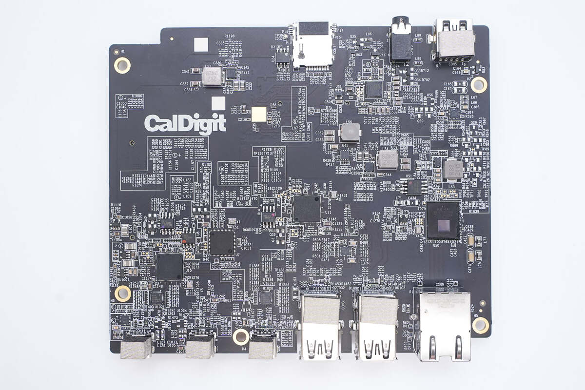
An overview of the PCBA modules and shielding cover.
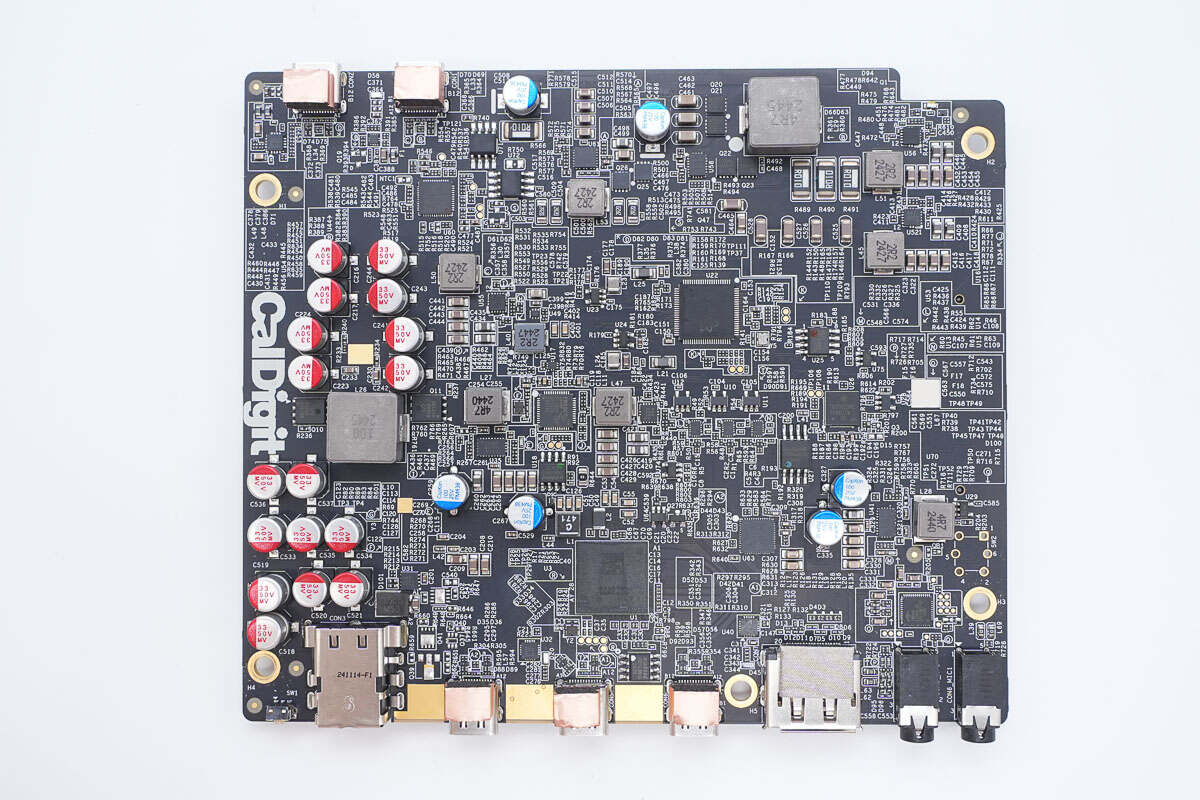
Front view of the Thunderbolt 5 interface PCB shows the power input, three Thunderbolt 5 ports, a DisplayPort 2.1 port, and a 3.5mm audio jack. Components include filter capacitors, alloy inductors, the Thunderbolt controller, a USB hub, and a USB-C controller.
The back side houses a synchronous buck-boost controller, MOSFETs, a USB-C controller, and a hot-plug controller.
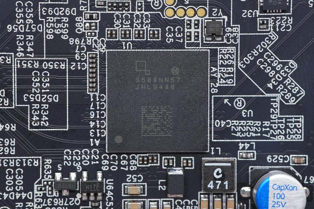
The Thunderbolt controller is from Intel, model JHL9480, codenamed Barlow Ridge. It supports four PCIe lanes configured as x4 Gen 4 and includes features such as ACS, FBP, PTM, and P2P, with support for 128/256-byte payloads.
For display ports, it offers 2 DP sinks and 3 DP sources, supporting DP 2.1 tunneling and retiming functions. It operates in x1, x2, and x4 modes with data rates ranging from 1.62 Gbps up to 20 Gbps. Additional features include SST, MST, DSC 1.2, FEC, LTTPR, and Panel Replay. The chip comes in an FC-CSP package.
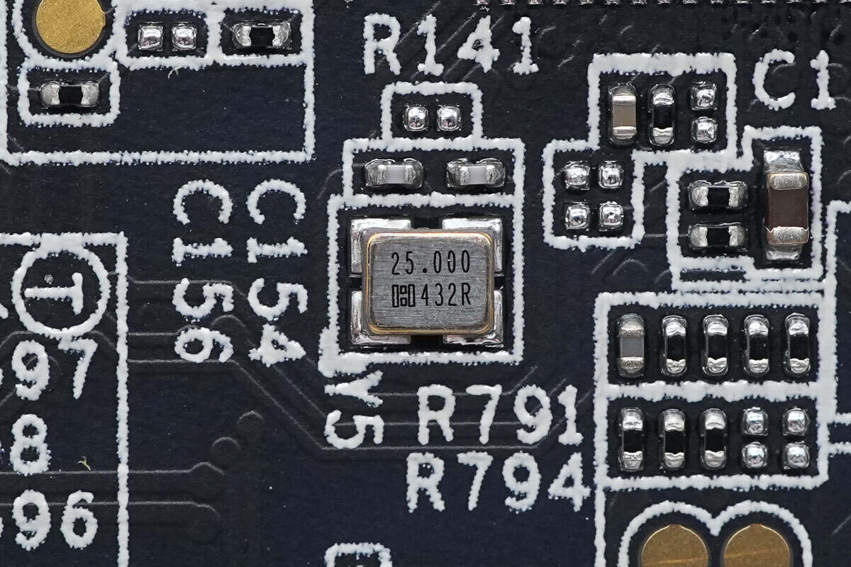
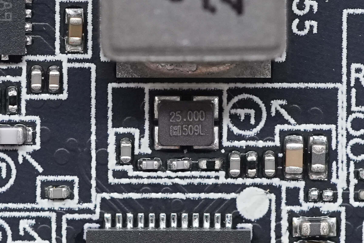
Close-up of the 25.000 MHz clock crystal oscillator.
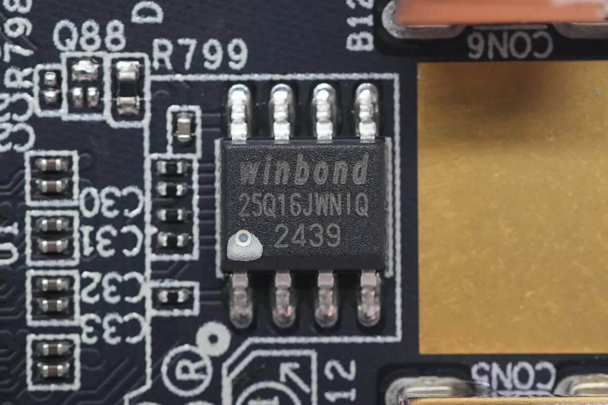
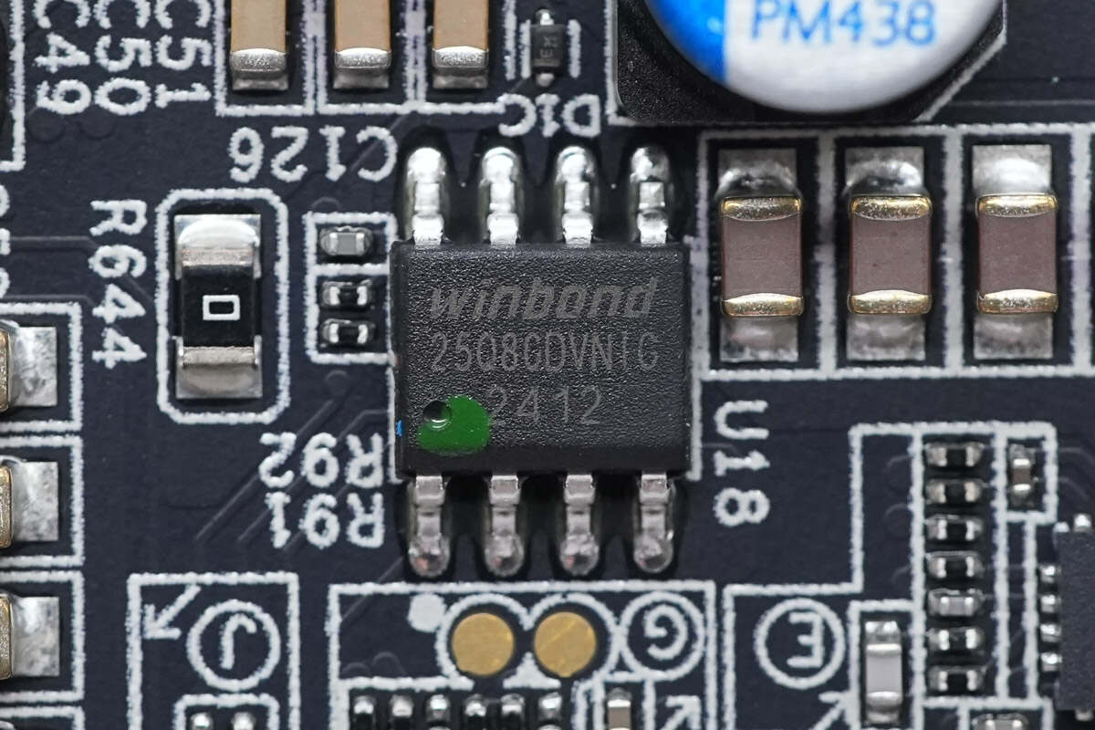
The memory chip is from Winbond, model W25Q16JWSNIQ, with a capacity of 2MB. It supports a 1.8V operating voltage and comes in an SOIC-8 package.
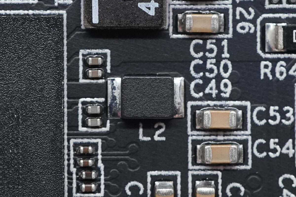
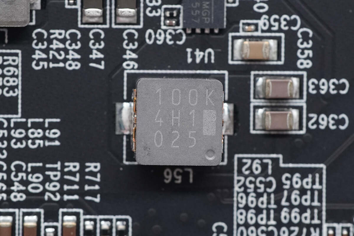
Close-up of the buck inductor.
Close-up of the 0.47μH buck inductor.
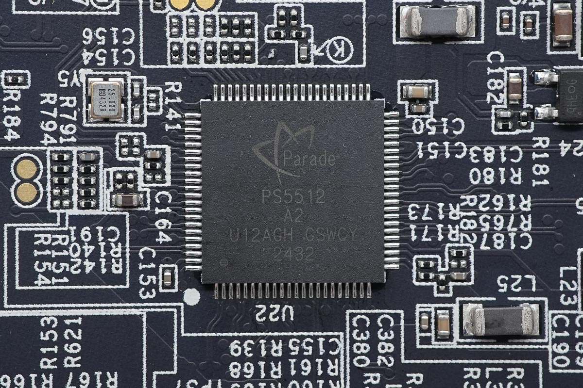
The USB hub is from Parade Technologies, model PS5512. It features four 10Gbps downstream ports—two USB-C and two USB-A—and includes an additional USB 2.0 port. The chip comes in a QFN88 package.
Close-up of the 25.000 MHz clock crystal oscillator.
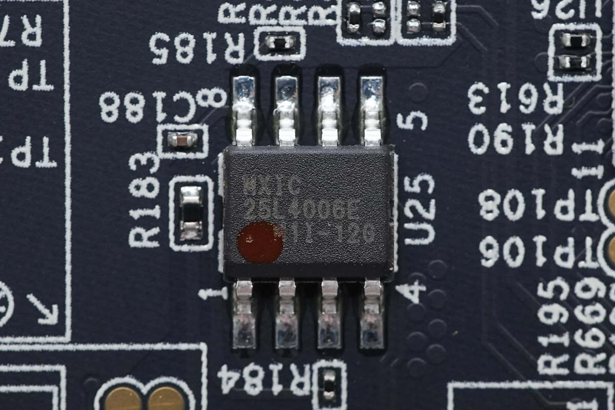
The memory chip is from MXIC, model MX25L4006E, with a capacity of 512KB. It supports a voltage range of 2.7–3.6V and comes in an SOP8 package.
The USB-C port controller is from Parade Technologies, model FL7112-2Q0. It supports dual USB-C port applications and integrates an MCU, voltage regulator, over-voltage protection, and over-temperature protection. The chip comes in a QFN48 package.
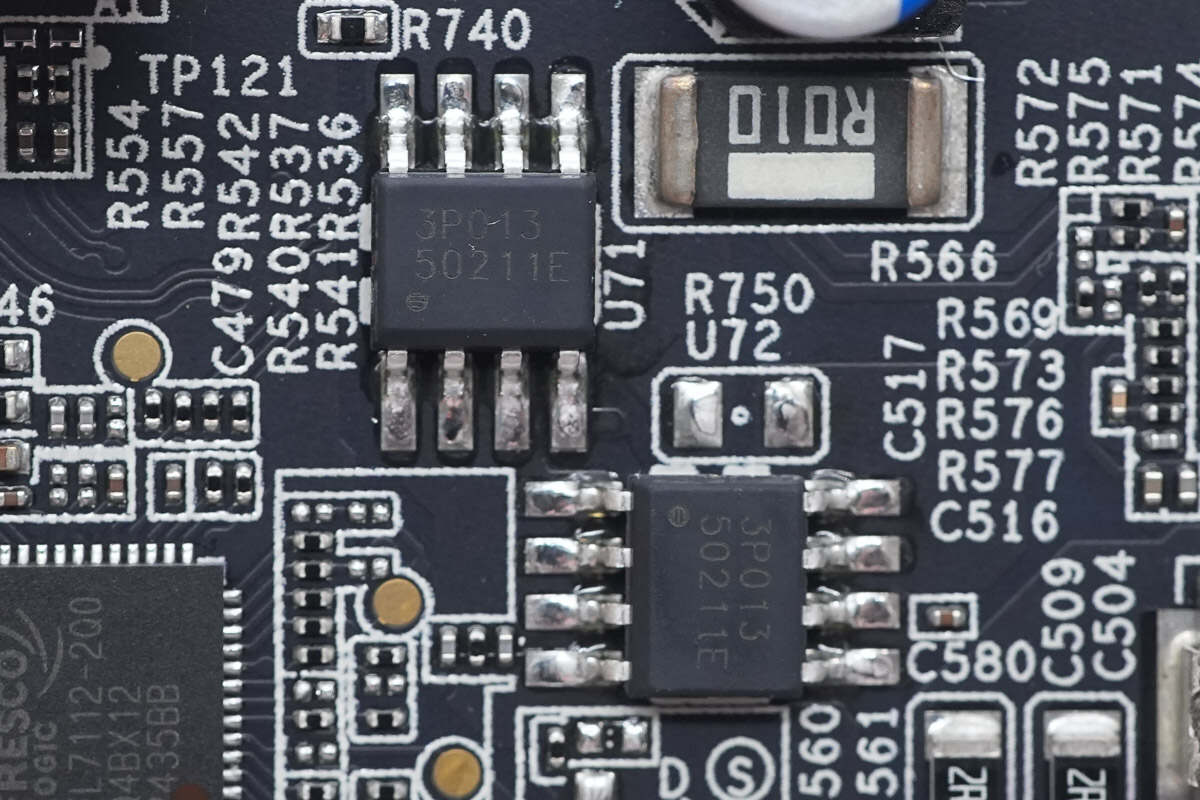
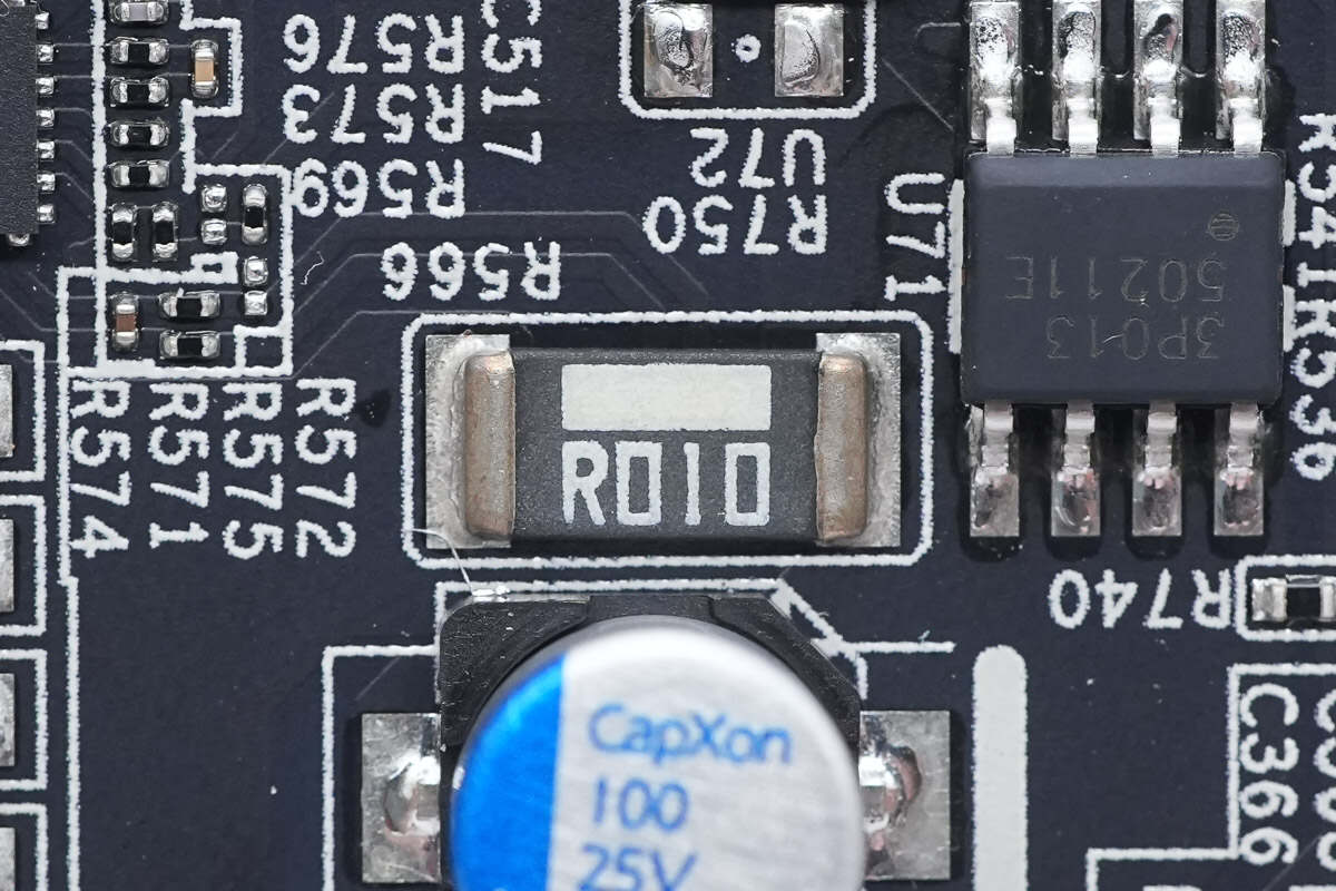
The VBUS MOSFETs are from APEC, model AP3P013M. They are P-channel MOSFETs with a voltage rating of -30V and an on-resistance of 13mΩ, packaged in SOP-8.
Close-up of the 10mΩ current sense resistor.
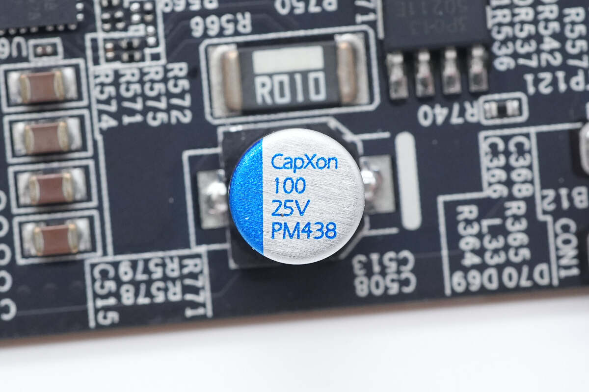
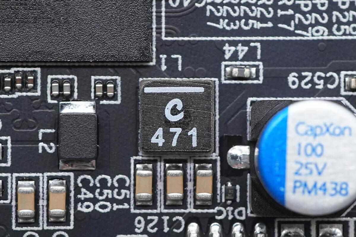
The filter capacitor is from CapXon, with a specification of 100μF 25V.
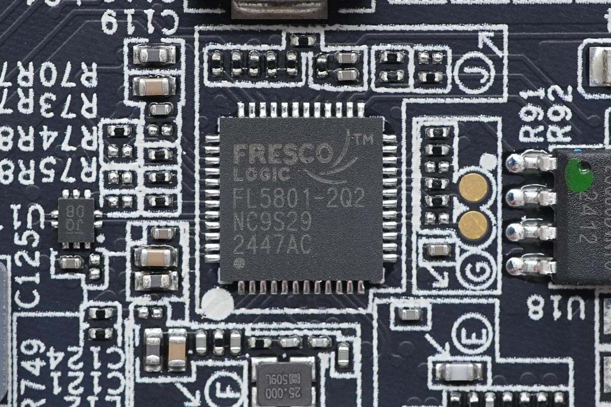
The hub chip is from Parade Technologies, model FL5801-2Q2. It is a USB 2.0 hub supporting configurations of 1 upstream port with 5 downstream ports, or 2 upstream ports with 4 downstream ports. It is backward compatible with USB 1.1, supports the BC1.2 specification, and offers customizable features. The chip comes in a QFN48 package.
Close-up of the 25.000 MHz clock crystal oscillator.
The memory chip is from Winbond, model W25Q80DVSNIG, with a capacity of 1MB. It supports a supply voltage range of 2.7–3.6V and comes in an SOIC-8 package.
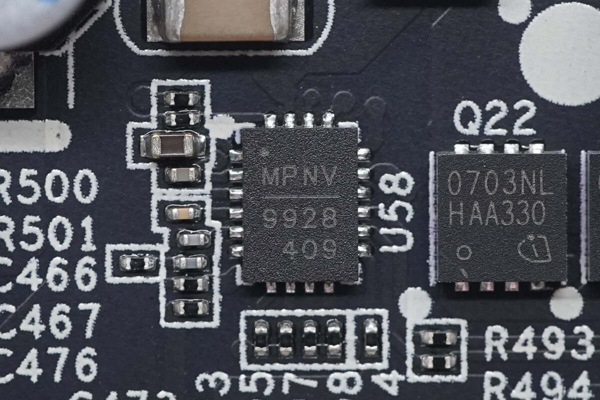
The buck controller is from MPS, model MP9928. It is a current-mode synchronous buck controller supporting up to 60V input voltage. It integrates a half-bridge NMOS driver, features a programmable operating frequency from 100kHz to 1MHz, supports phase-shifted outputs, cycle-by-cycle overcurrent protection, output overvoltage protection, and high-precision over-temperature protection. The chip comes in a QFN20 package.

The synchronous buck MOSFETs are from Infineon, marked with "0703NL," model ISZ0703NLS. They are N-channel MOSFETs rated for 60V with an on-resistance of 7.3mΩ, packaged in a TSDSON-8 FL.
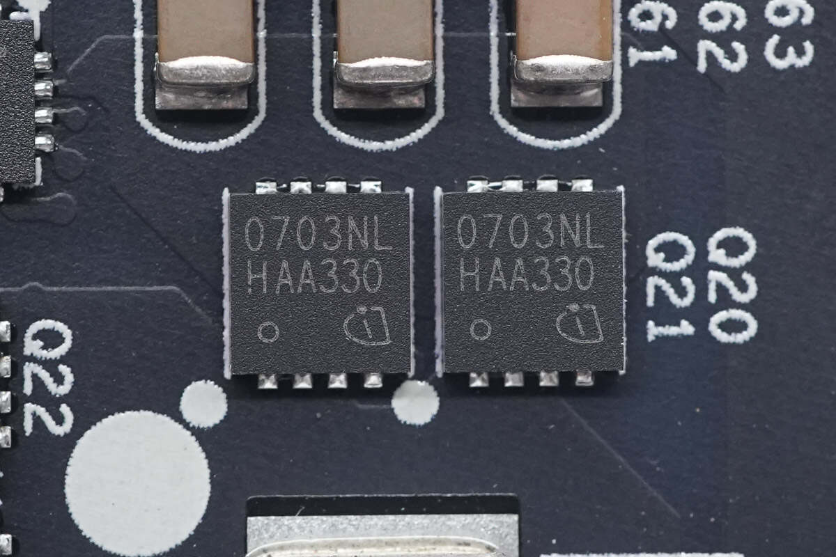
The other two MOSFETs have the same model.
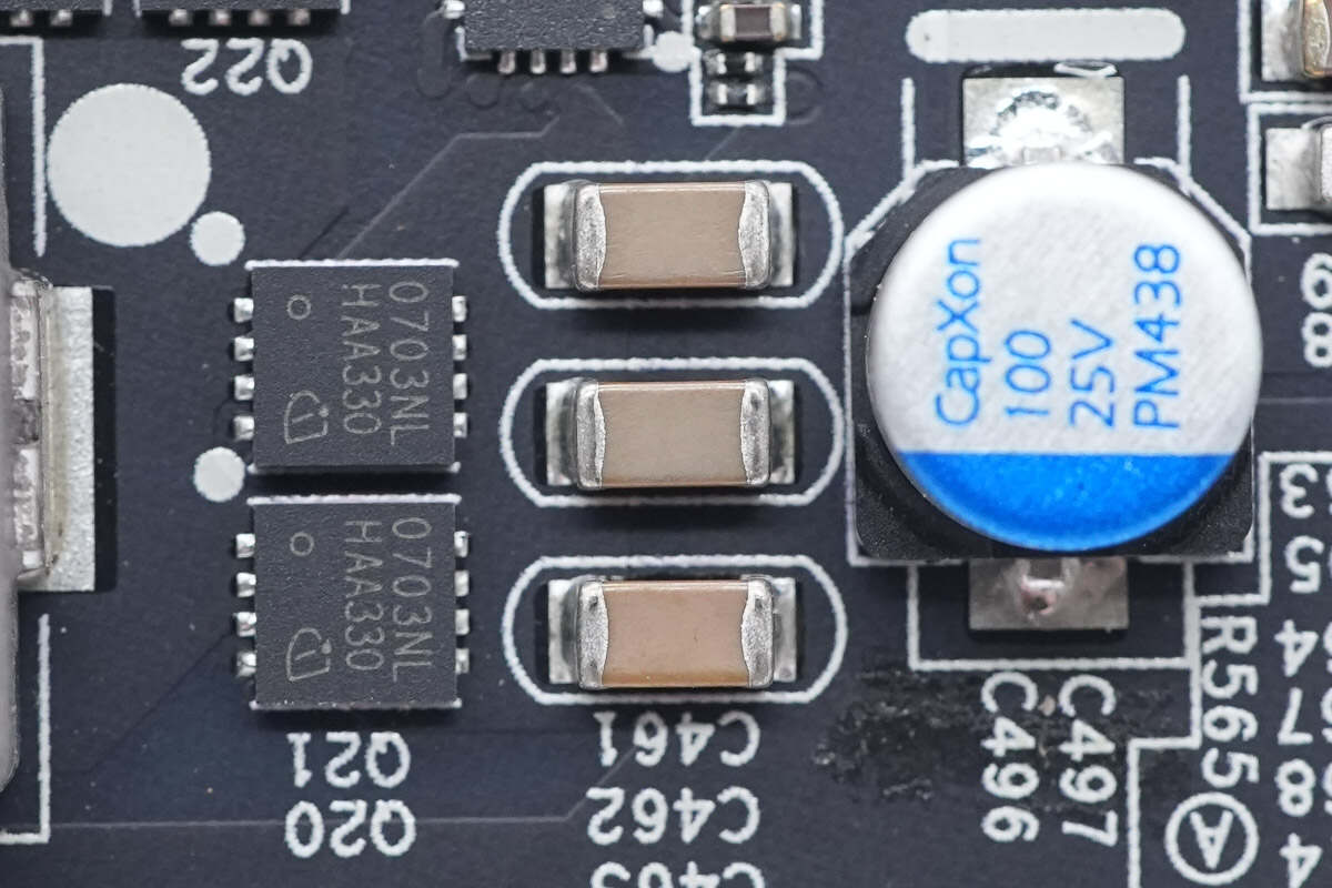
The MLCC filter capacitors are in a 1206 package size.
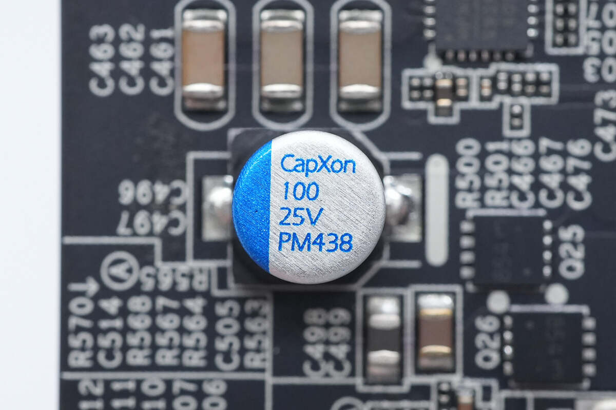
The filter capacitor is from CapXon, rated at 100μF 25V.
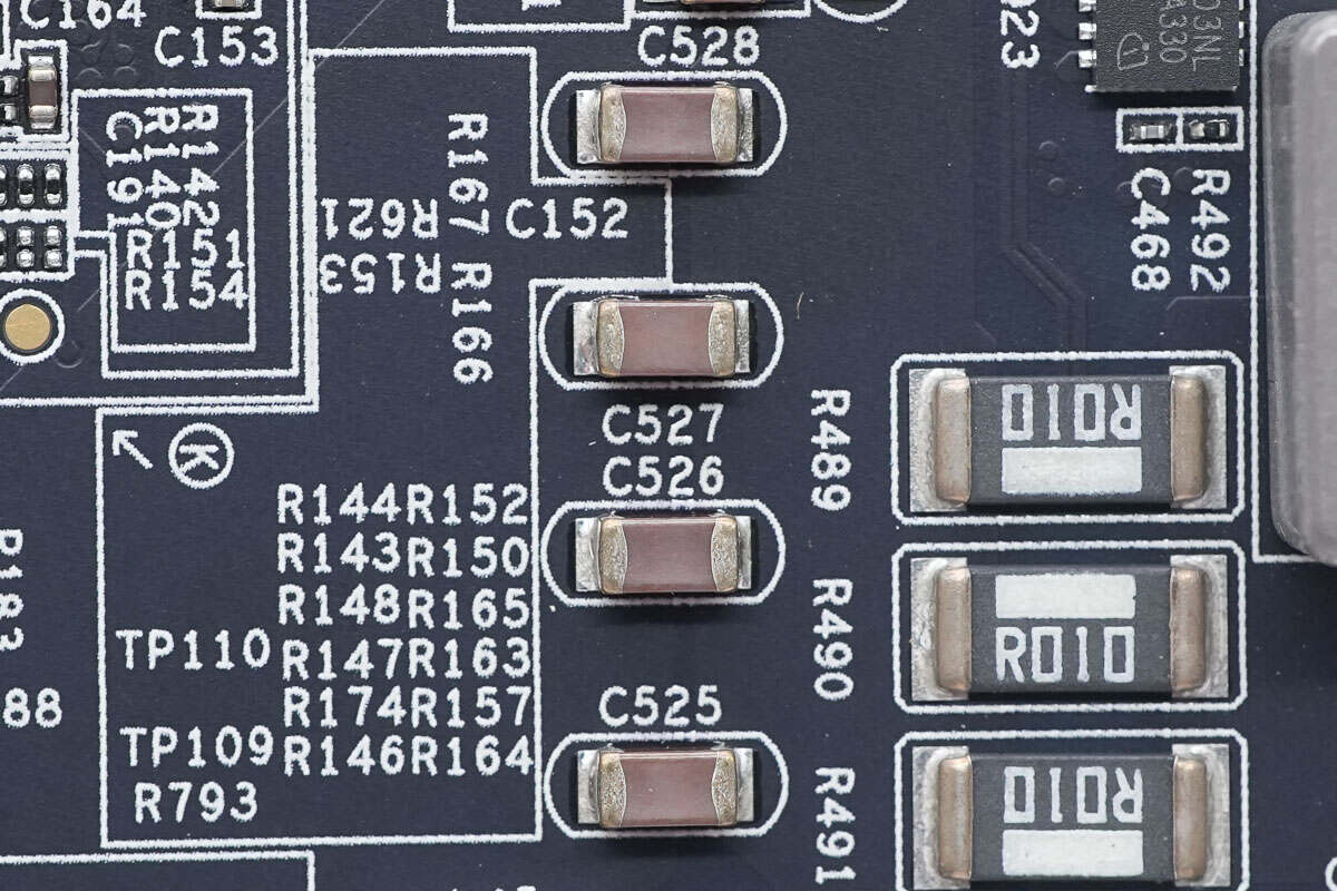
Close-up of the output filtering MLCC capacitors.
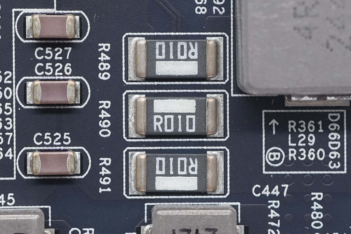
Three 10mΩ resistors are connected in parallel for output current sensing.

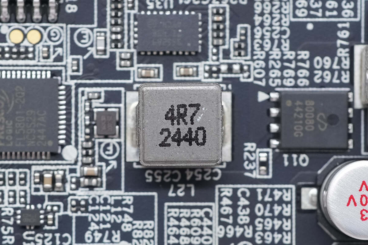
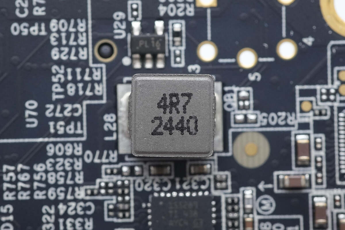
Close-up of the 4.7μH alloy inductor.
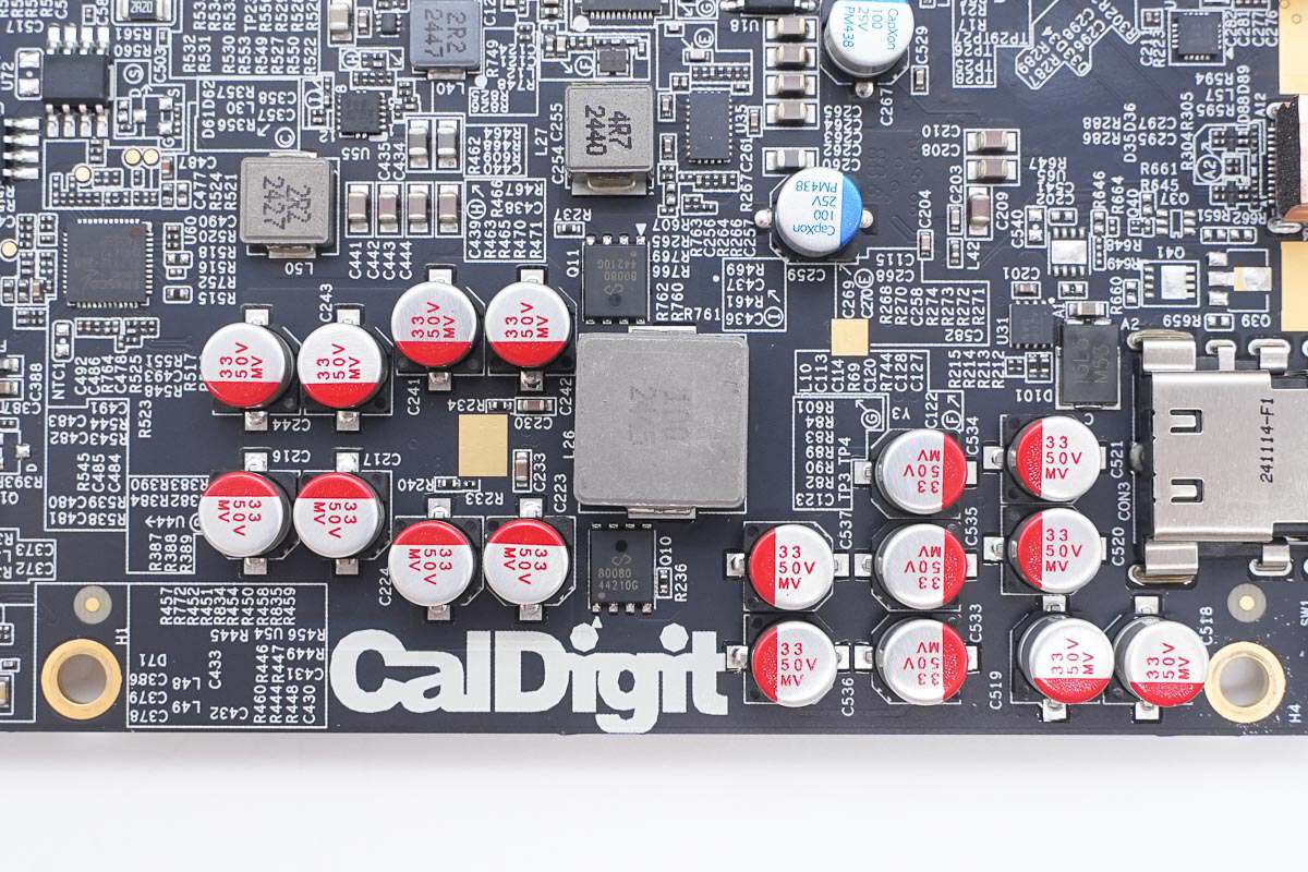
A total of 17 SMD filter capacitors are used on both the input side and the synchronous buck-boost converter.

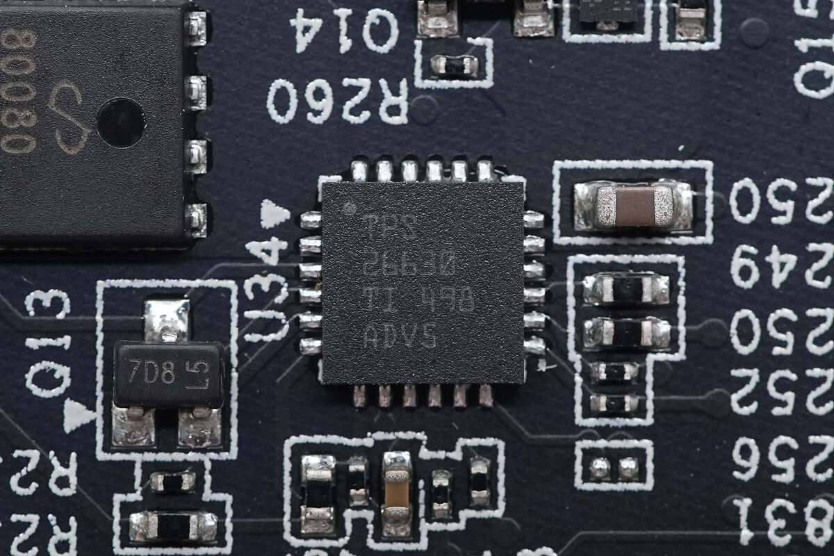
The synchronous buck-boost controller is from Texas Instruments, model BQ25758. It supports an input voltage range of 4.2–60V and an output voltage range of 3.3–60V, with bidirectional conversion capability. The chip supports USB PD ERP applications, constant voltage and constant current control, and can operate in buck mode. It offers I²C control and resistor-programmed current limiting, making it suitable for hubs, monitors, and docking station applications. The package type is QFN36.

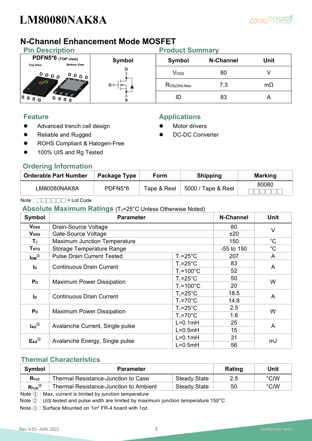
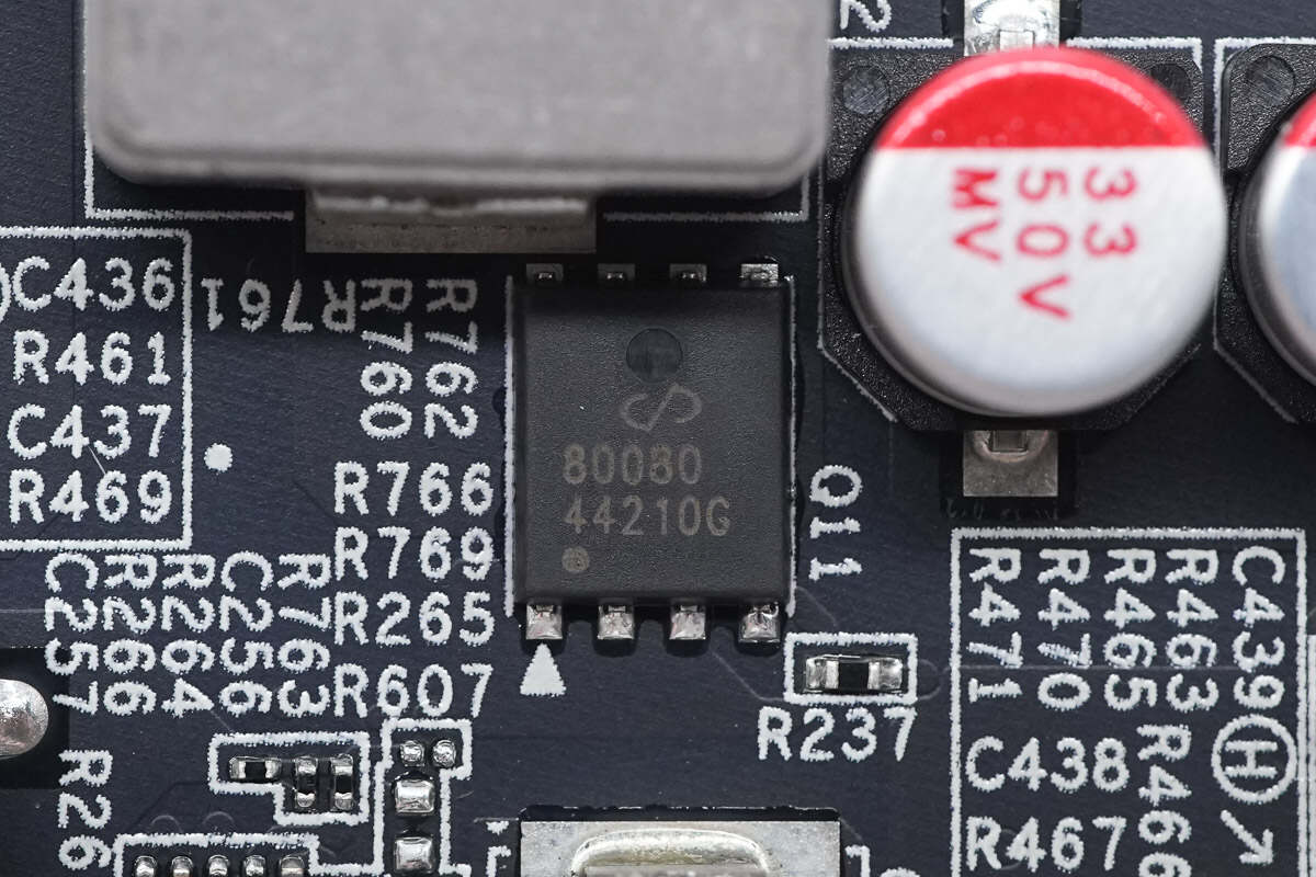
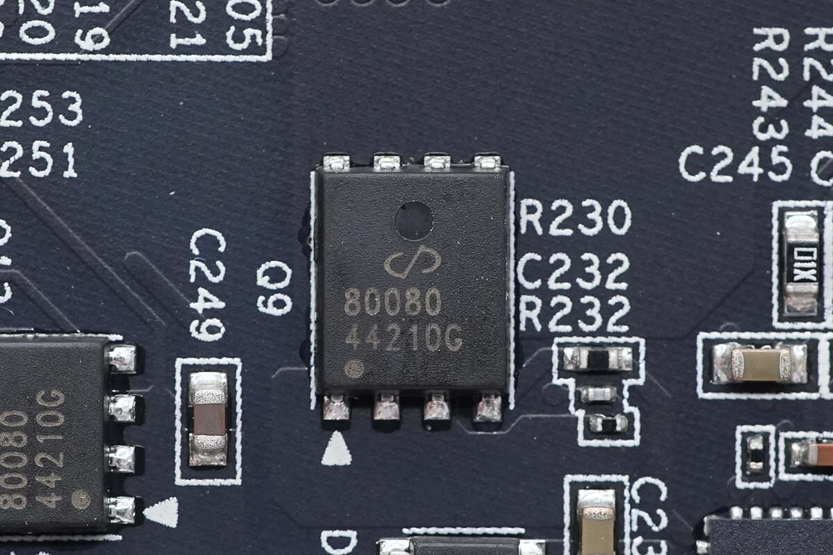
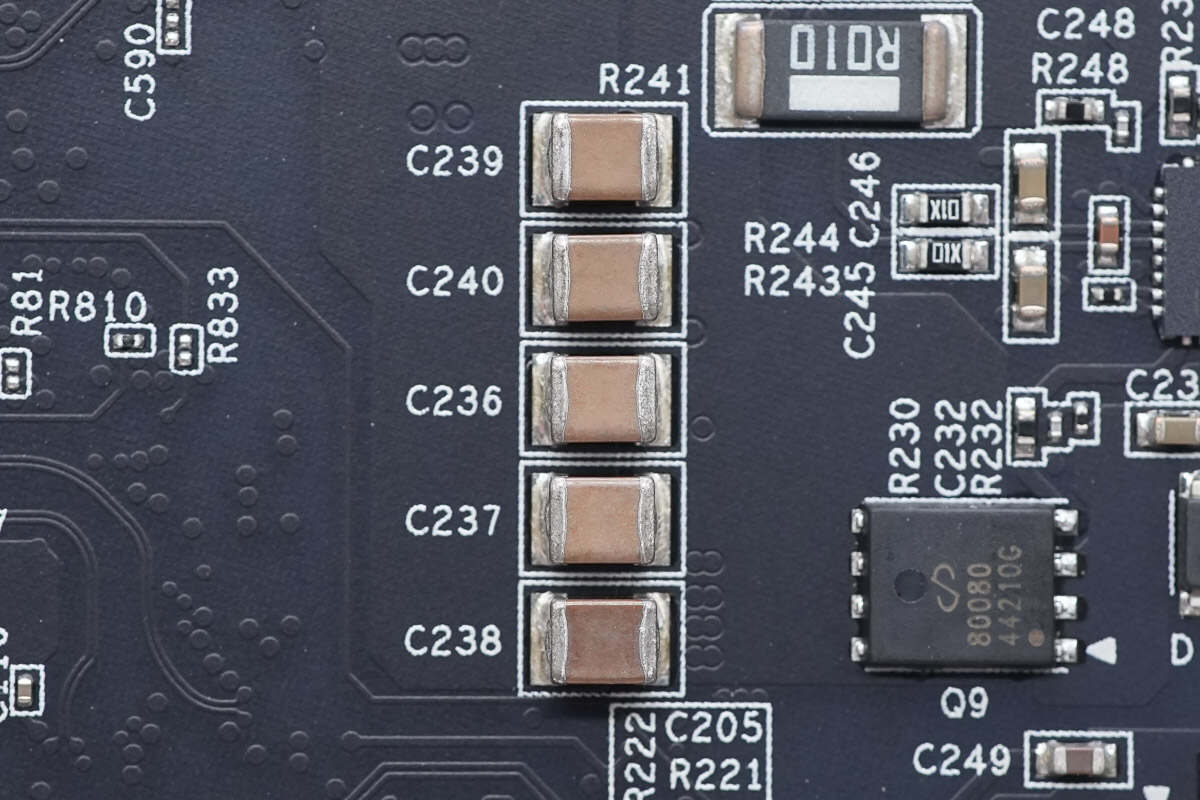
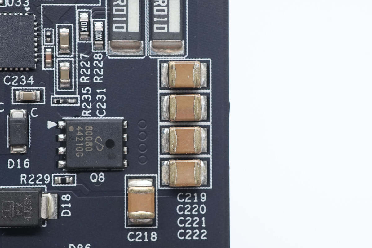
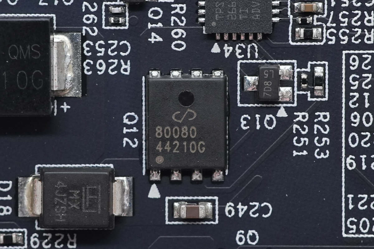
The synchronous buck-boost MOSFET is from Leadpower, marked with "80080," model LM80080NAK8A. It is an N-channel MOSFET with an 80V voltage rating and 7.3mΩ on-resistance. Designed for motor drive and DC-DC conversion applications, it comes in a PDFN 5×6 package.
Here is the information about Leadpower LM80080NAK8A.
The synchronous buck-boost circuit uses four identical MOSFETs. Here is a close-up of the second MOSFET of the same model.
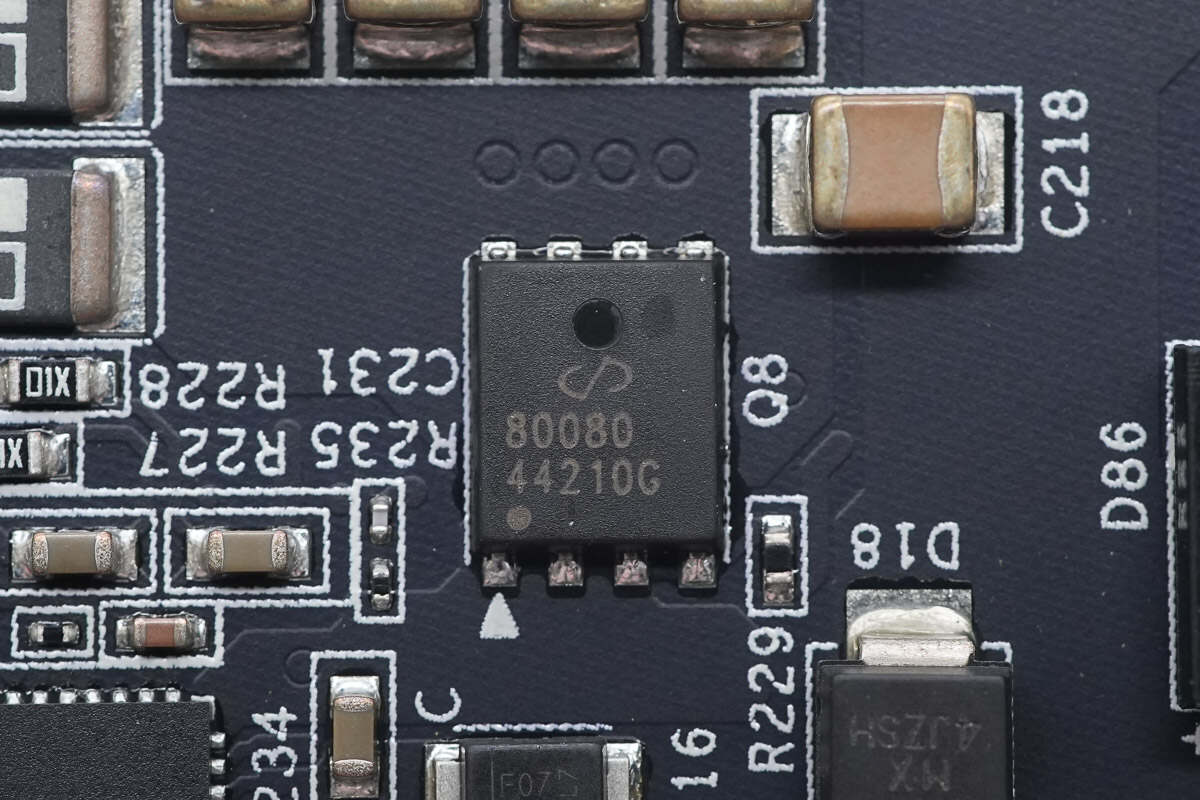
Close-up of the third MOSFET of the same model.
All four MOSFETs share the same model.
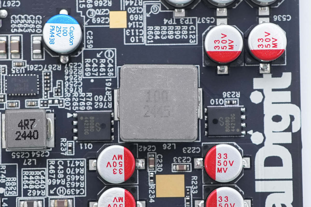
The 10μH alloy inductor is used for buck-boost voltage conversion.
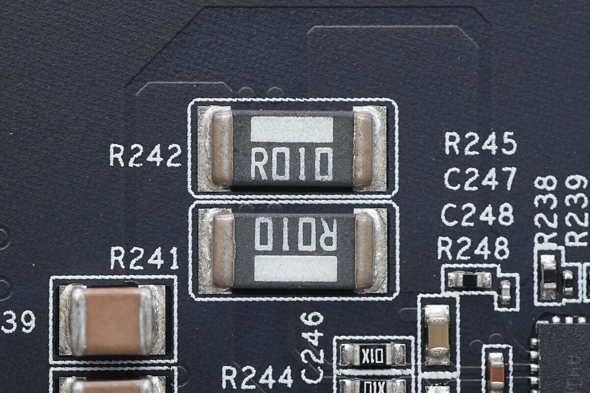
Close-up of the 10mΩ current sense resistors.

There are also two 10mΩ current sense resistors located on the outer side.
Close-up of five 1210 package MLCC capacitors connected in parallel.
The other side features four MLCC capacitors connected in parallel.
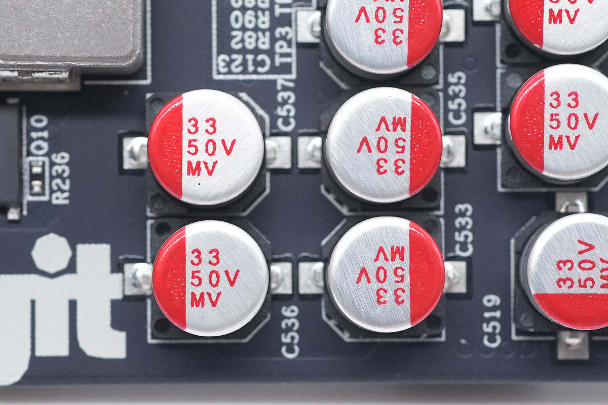
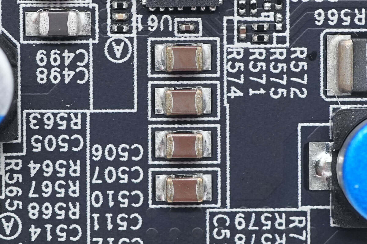
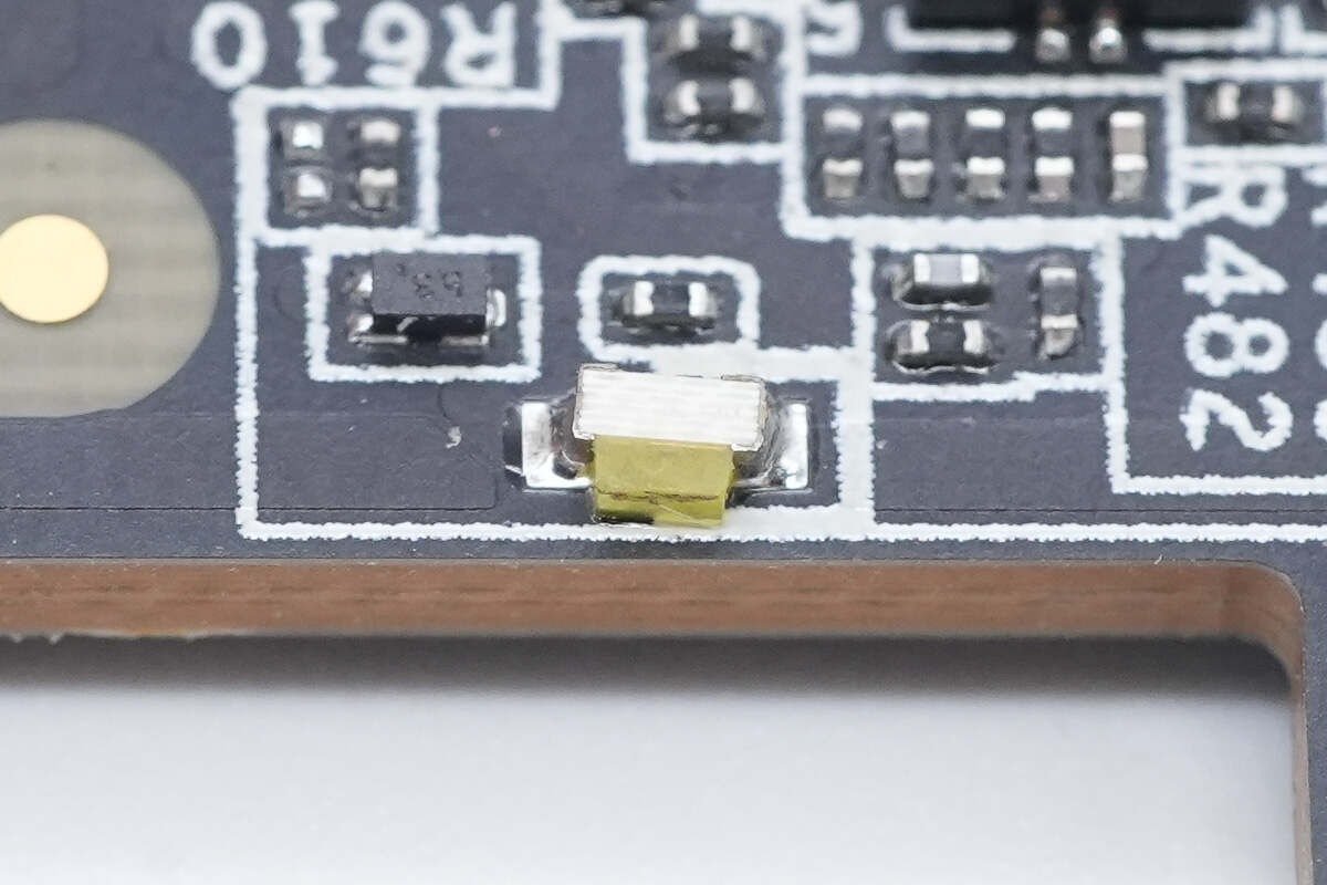
The filter capacitors are from TRUSTCAP, part of the TPMV series of SMD capacitors. They are rated at 33μF 50V and support an operating temperature range of -55°C to 105°C. With a height of only 5.5mm, these ultra-compact capacitors are among the few in the industry that effectively support modern digital chips and high-frequency switching filtering, absorbing power supply noise. They also comply with RoHS and REACH standards and are halogen-free.
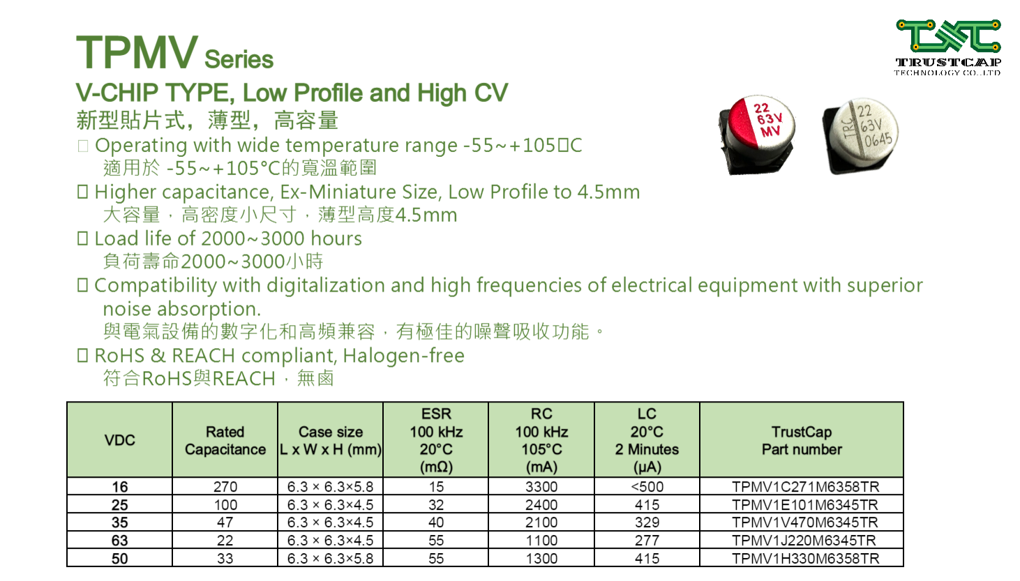
Here is the information about the TRUSTCAP TPMV series of SMD capacitors.
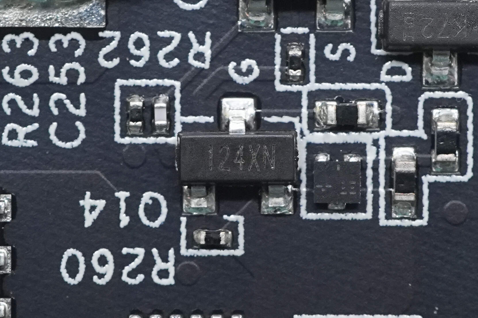
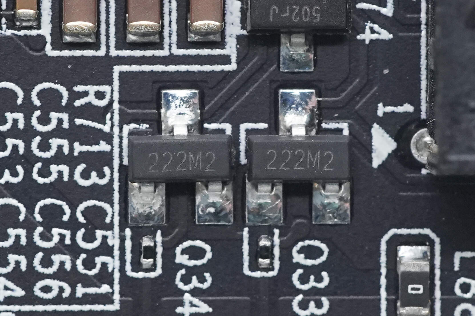
The MOSFET is from Leadpower, marked with "12," model LM60M80PEI3A. It is a P-channel MOSFET rated for -60V with an on-resistance of 4.3Ω. It is suitable for general switching and analog switch applications and comes in an SOT-23 package.
Here is the information about Leadpower LM60M80PEI3A.
The MOSFETs are from Leadpower, marked with "22," model LM30320NLI3A. They are N-channel MOSFETs rated for 30V with an on-resistance of 32mΩ. These are suitable for load switch and DC-DC converter applications and come in an SOT-23 package.
Here is the information about Leadpower LM30320NLI3A.
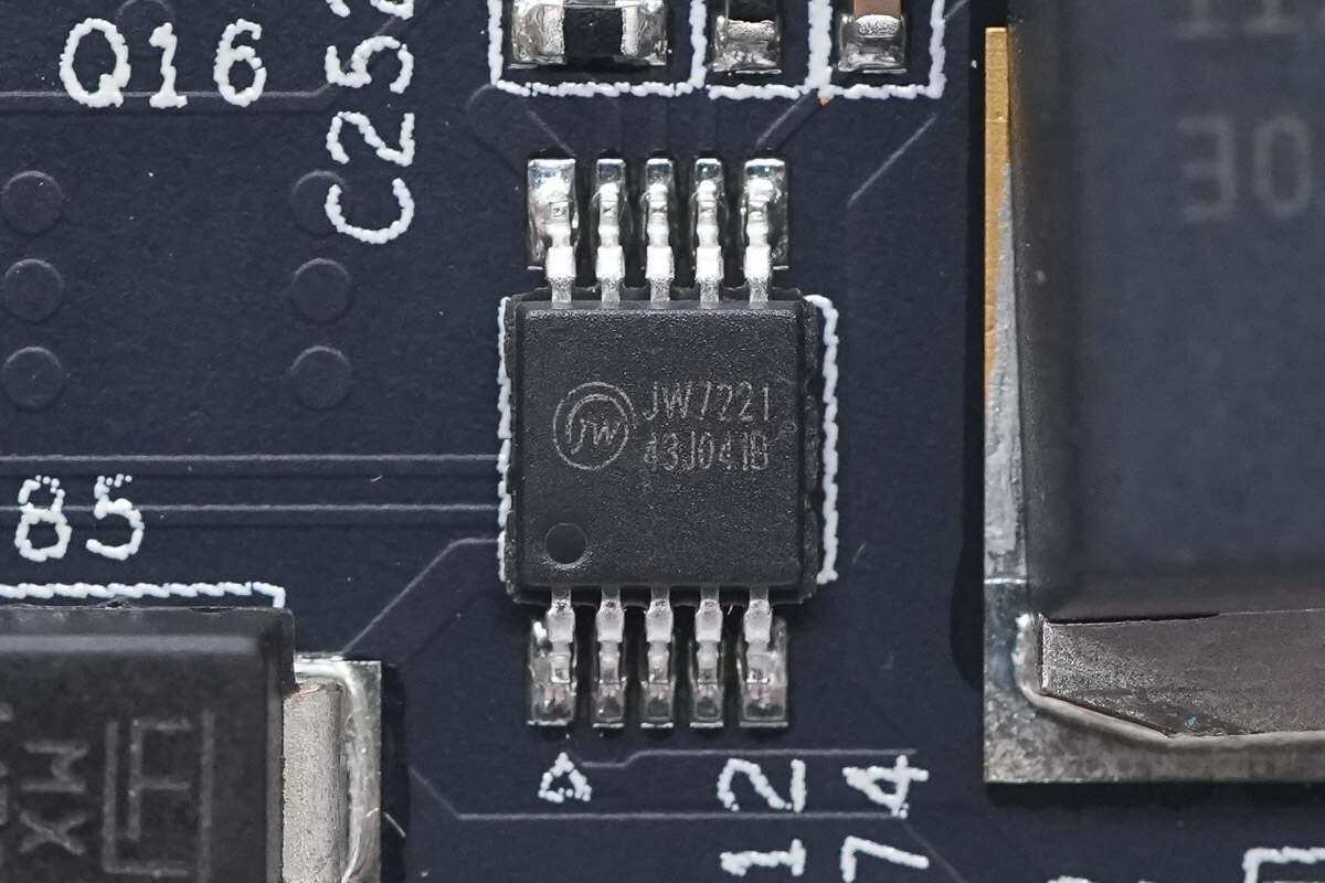
The hot-plug controller is from JOULWATT, model JW7221. It is a high-side hot-plug and inrush current controller with power limiting capabilities, supporting an input voltage range of 9–80V. The chip features programmable power limit and surge current protection, integrates an internal charge pump and NMOS driver, and is available in both latch and self-recovery versions. It comes in an MSOP-10 package.
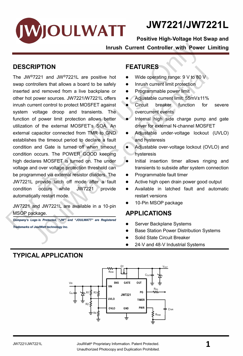
Here is the information about JOULWATT JW7221.
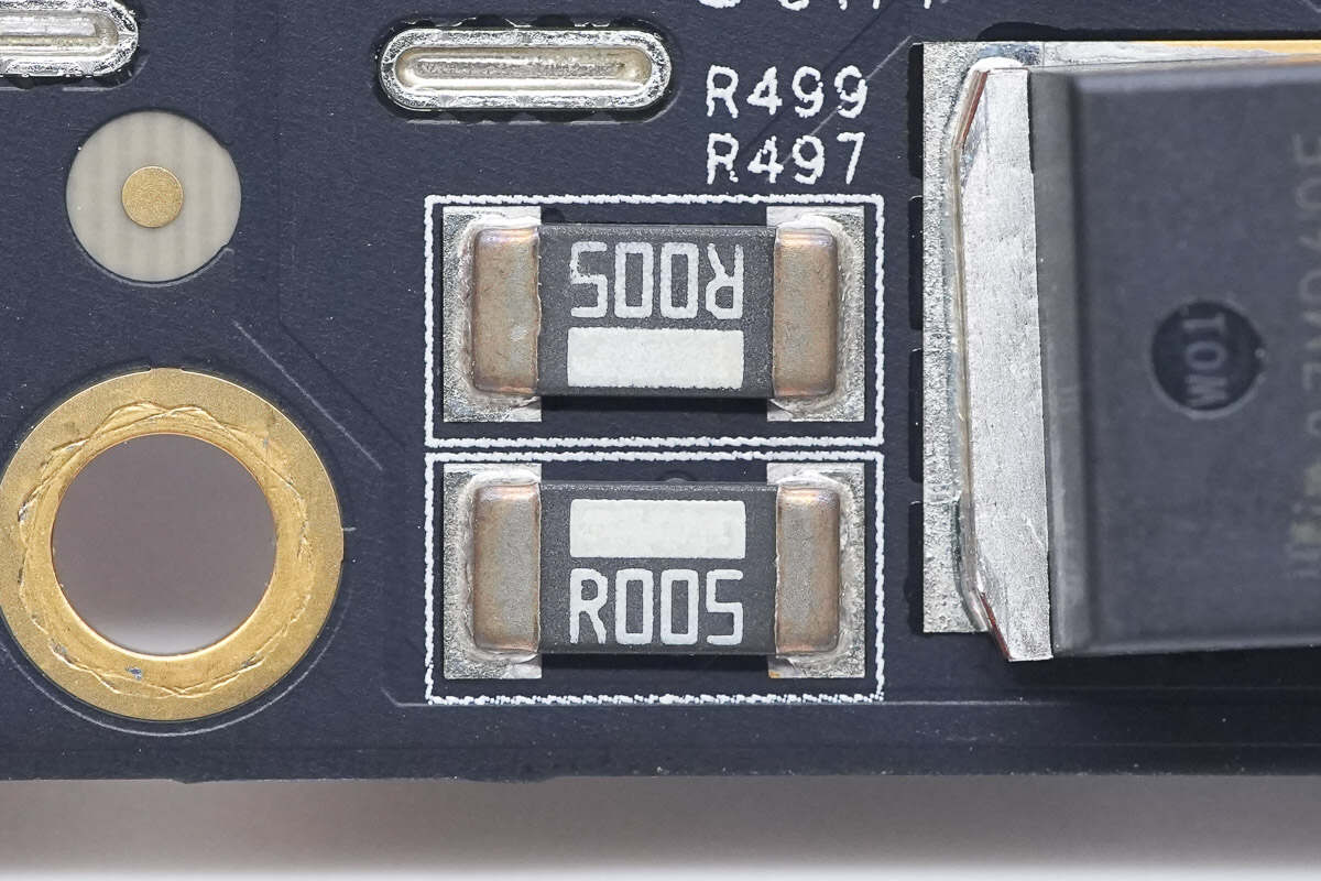
Two 5mΩ sense resistors are used for input current detection.
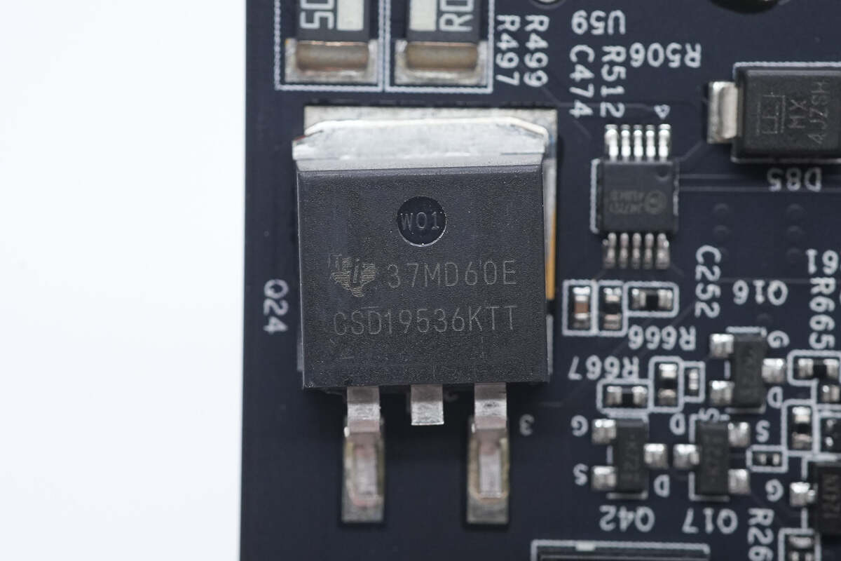
The hot-plug MOSFET is from Texas Instruments, model CSD19536KTT. It is an N-channel MOSFET rated for 100V with an on-resistance of 2.4mΩ, packaged in a D2PAK.
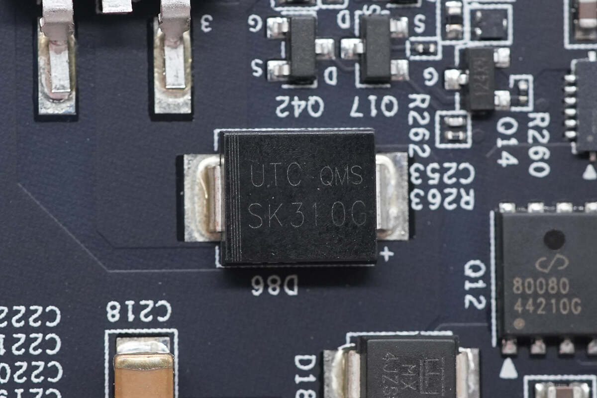
The Schottky diode is from Unisonic, model SK310G, rated at 100V and 3A, and comes in an SMC package.
The electronic fuse is from Texas Instruments, model TPS2663. It features output power limiting and surge protection, supports an input voltage range of 4.5–60V, and integrates a 60V-rated, 31mΩ on-resistance hot-plug MOSFET. It supports a current limit of 6A and comes in a VQFN24 package.
An external Leadpower LM80080NAK8A MOSFET is used for reverse polarity protection and reverse current blocking.
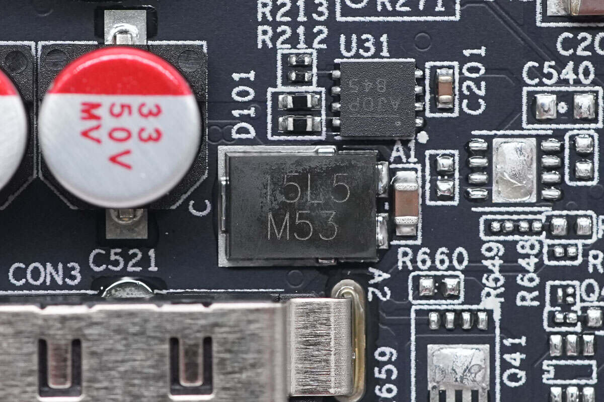
The Schottky diode, marked with "15L5," is rated at 15A 50V. It is used for input reverse polarity protection and comes in a TO-277 package.
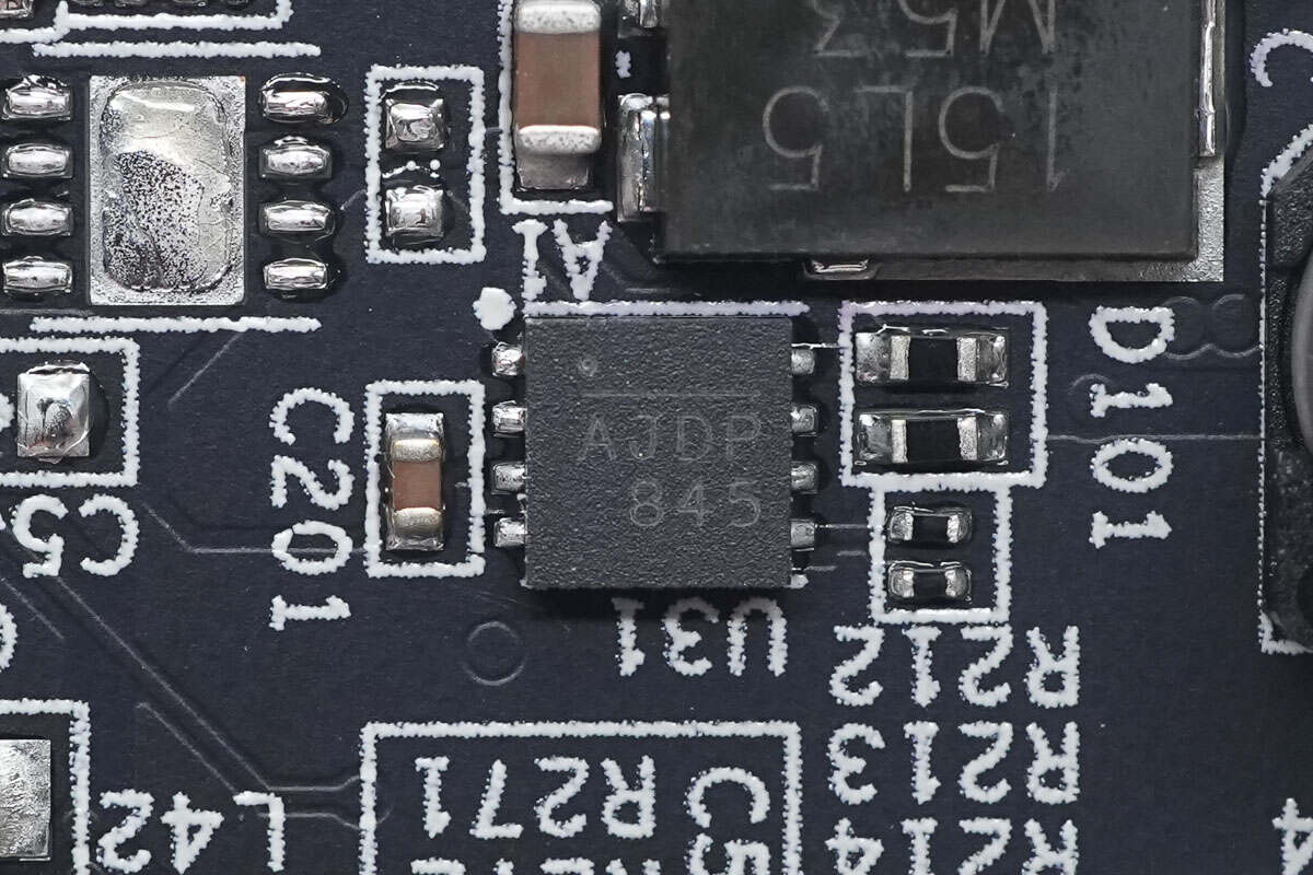
The voltage regulator chip is from MPS, marked with "AJD," model MP2013A. It is a low quiescent current, low dropout regulator with an input voltage range of 2.5–40V and an output current of 150mA. The chip comes in a QFN8 package.

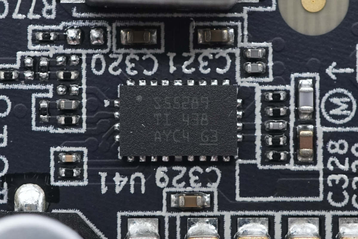
The synchronous buck-boost converter for the Thunderbolt 5 interface’s 36W fast charging output is from Texas Instruments, model TPS55289. It integrates internal MOSFETs and supports an input voltage range of 3–30V and an output voltage range of 0.8–22V. It features output overvoltage protection, average inductor current limit, cycle-by-cycle peak current limit, and output short-circuit protection. The chip is packaged in a VQFN-HR 21.
Close-up of the 4.7μH alloy inductor.
The other channel also uses the Texas Instruments TPS55289 synchronous buck-boost converter.
Close-up of the 4.7μH alloy inductor.
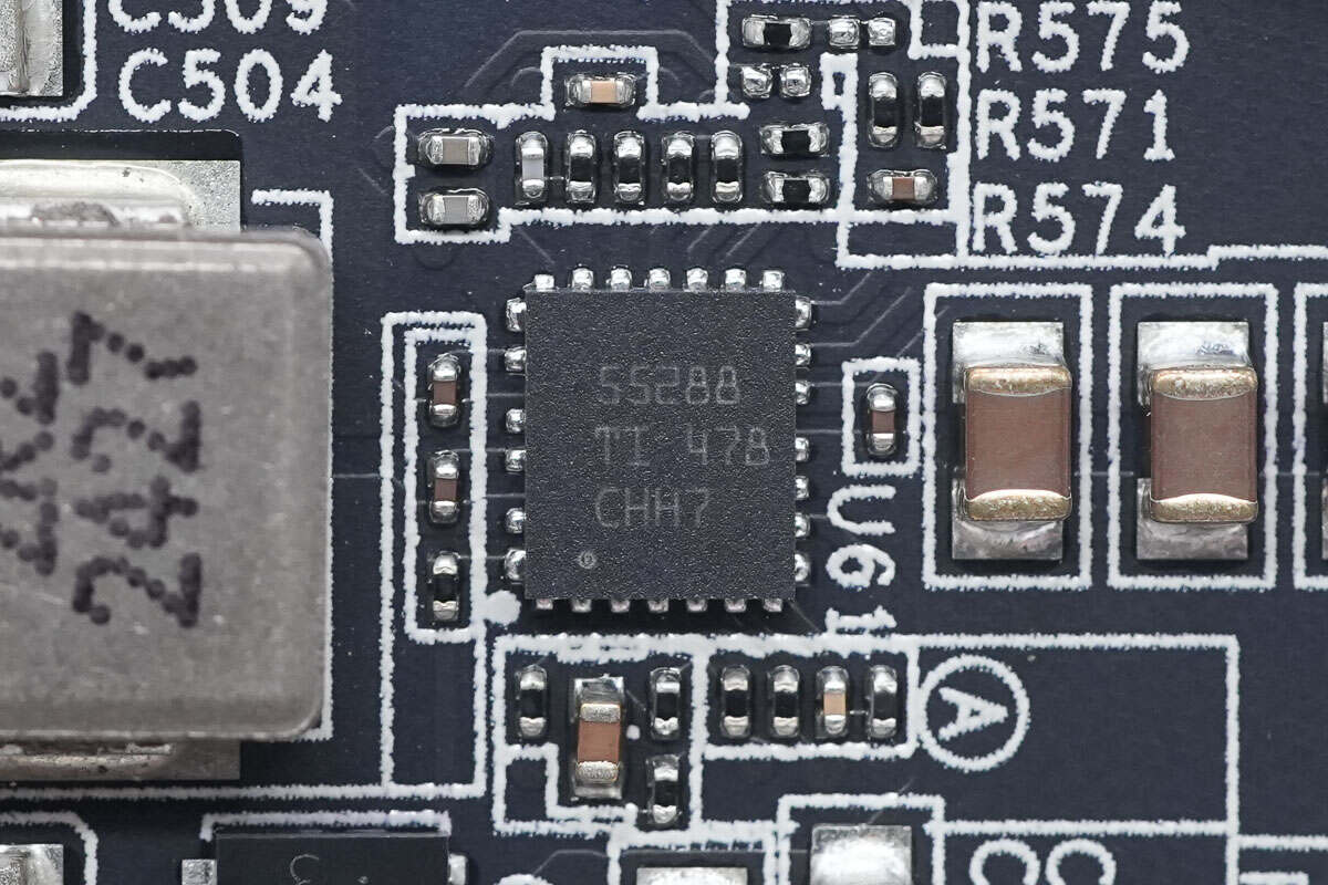
The synchronous buck-boost converter is from Texas Instruments, model TPS55288. It supports an input voltage range of 2.7–36V and an output voltage range of 0.8–22V. The chip integrates two internal MOSFETs and requires two external MOSFETs. It features output overvoltage protection, average inductor current limit, cycle-by-cycle peak current limit, and output short-circuit protection. The package type is VQFN-HR 26.

The two MOSFETs are marked with "854."

Close-up of the 2.2μH alloy inductor.
Close-up of four MLCC capacitors connected in parallel.
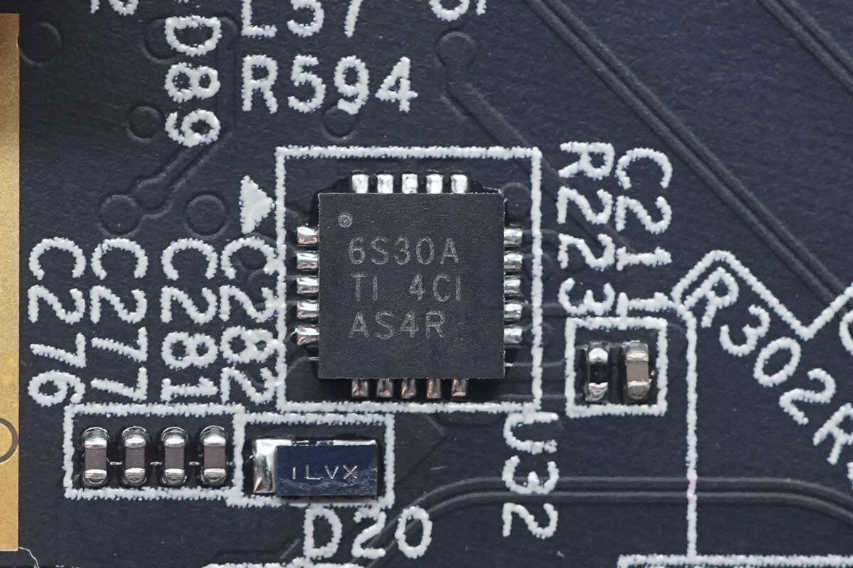
The USB-C port protector is from Texas Instruments, marked with "6S30A," model TPS6S300A. It provides 4-channel VBUS short-circuit and overvoltage protection, along with 6-channel ESD protection. The device comes in a WQFN20 package.
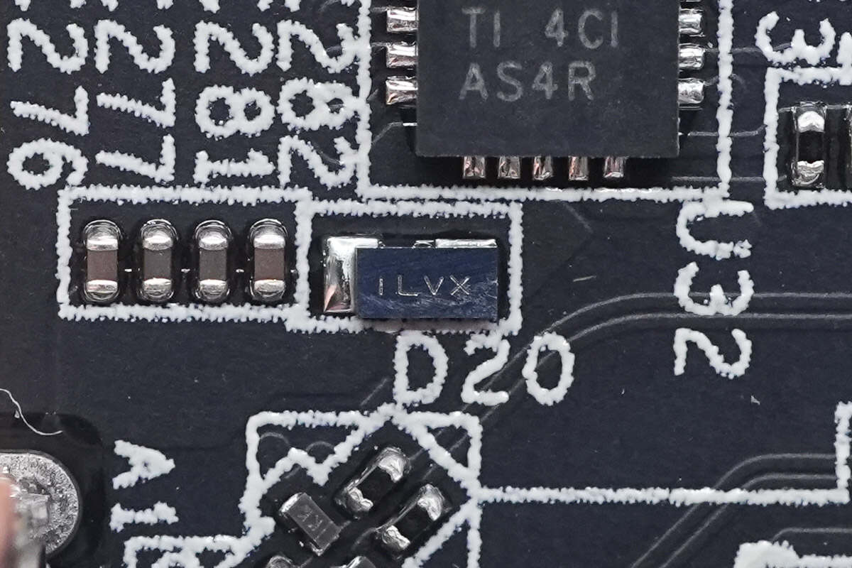
The Schottky diode is from Onsemi, marked with "LV," model NSR20F30NXT5G. It is rated for 30V and 2A, and comes in a DSN2 package.
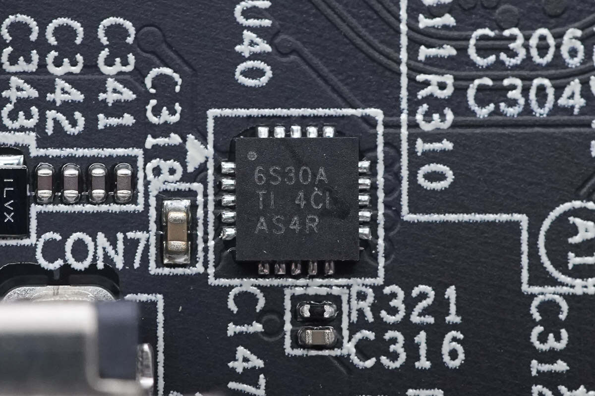
The other USB-C port protector also uses the Texas Instruments TPS6S300A.
The external diodes share the same model.
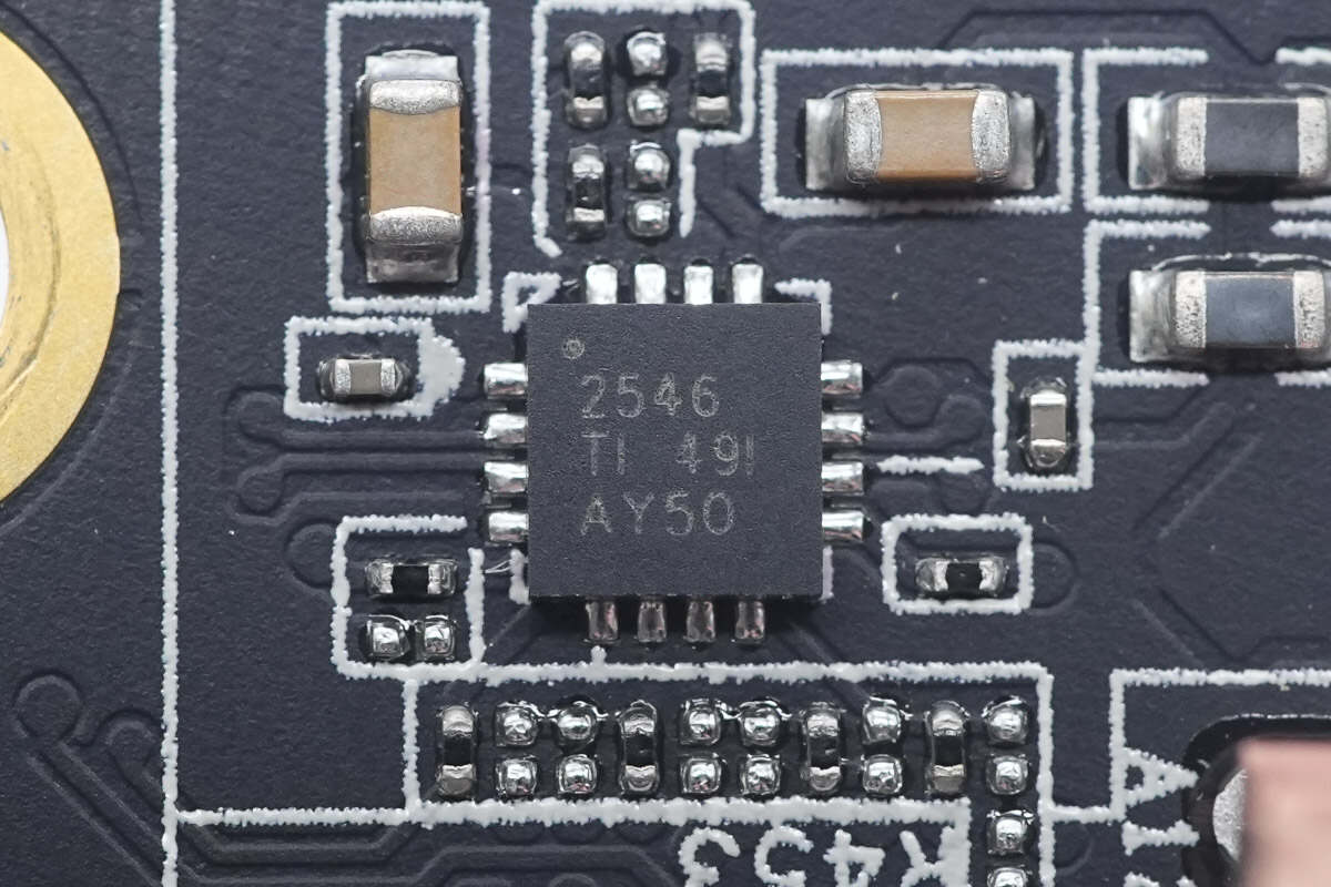
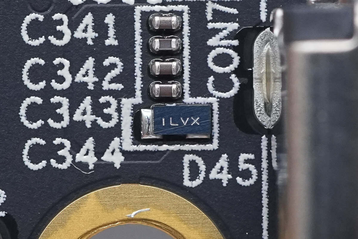
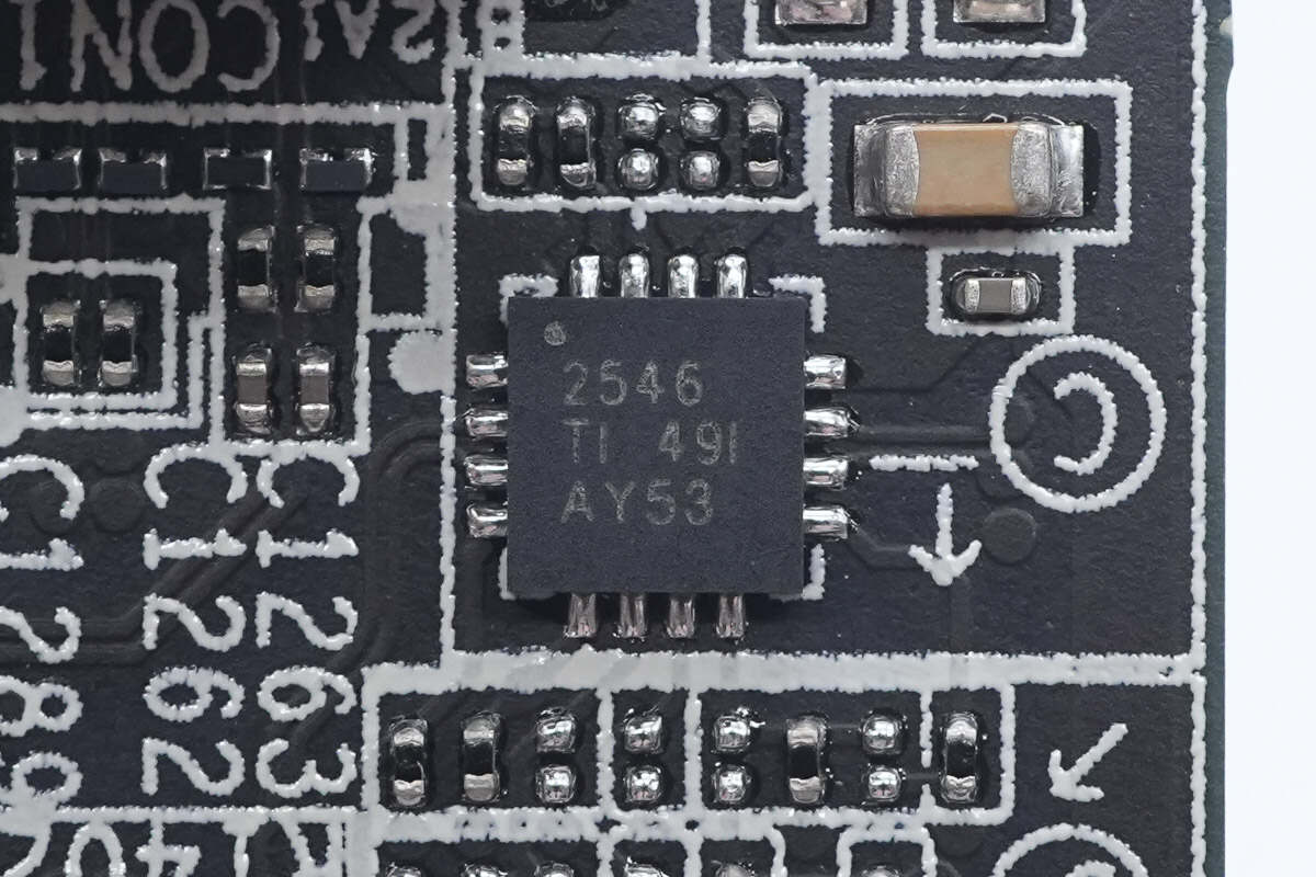
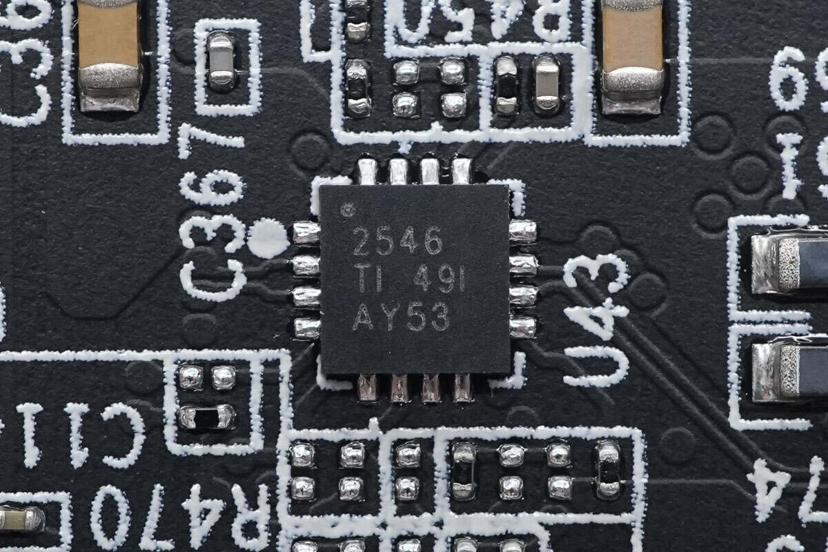
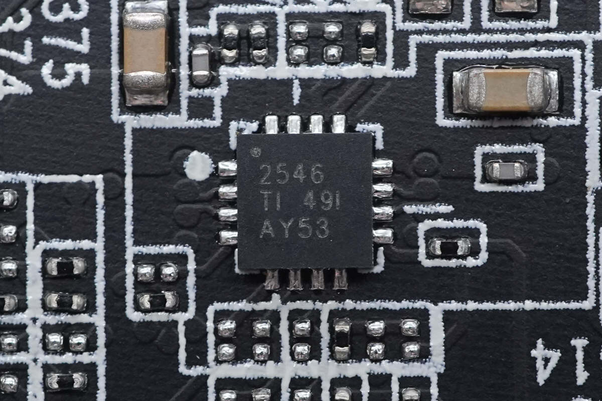
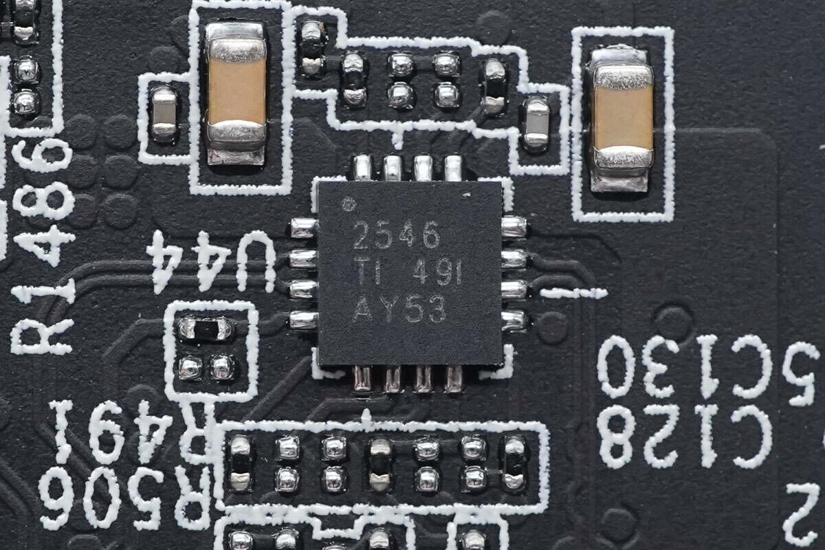
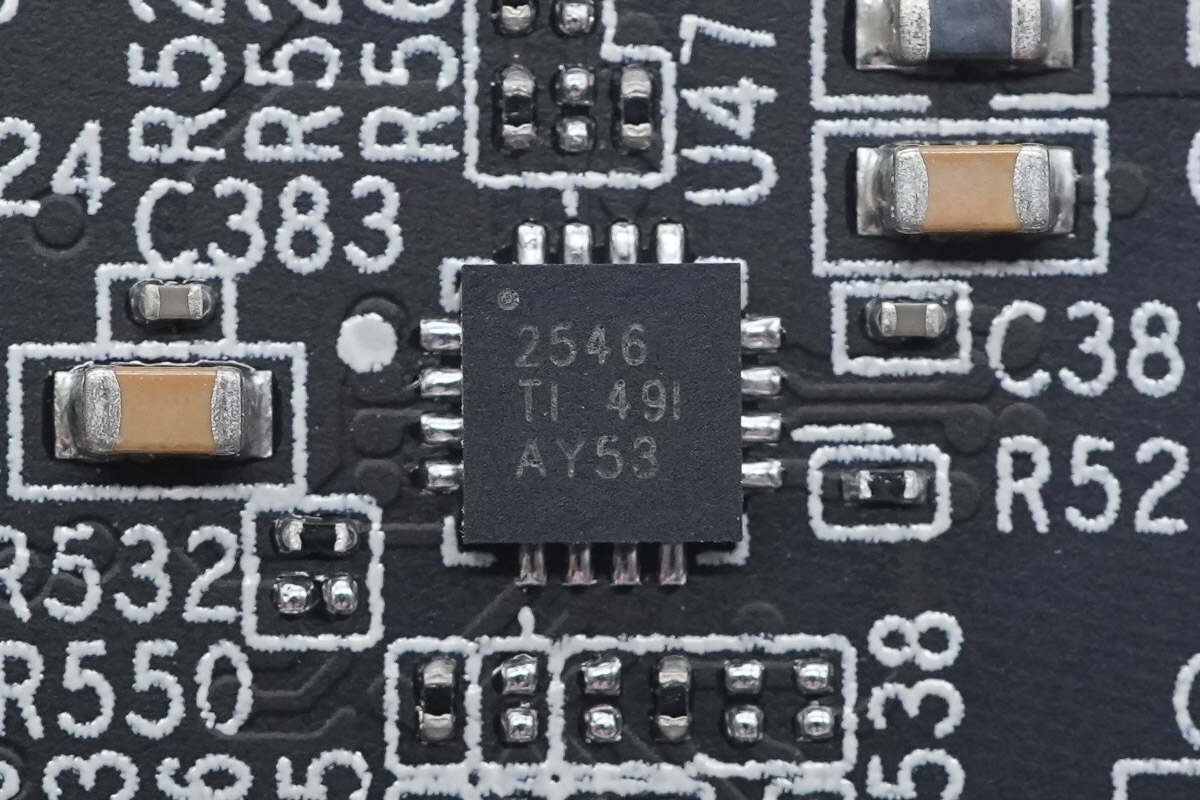
The charging port controller and load switch for the USB interfaces are from Texas Instruments, model TPS2546. It features an integrated 73mΩ high-side MOSFET, supports up to 3A output current, operates within a 4.5–5.5V voltage range, and comes in a WQFN16 package.
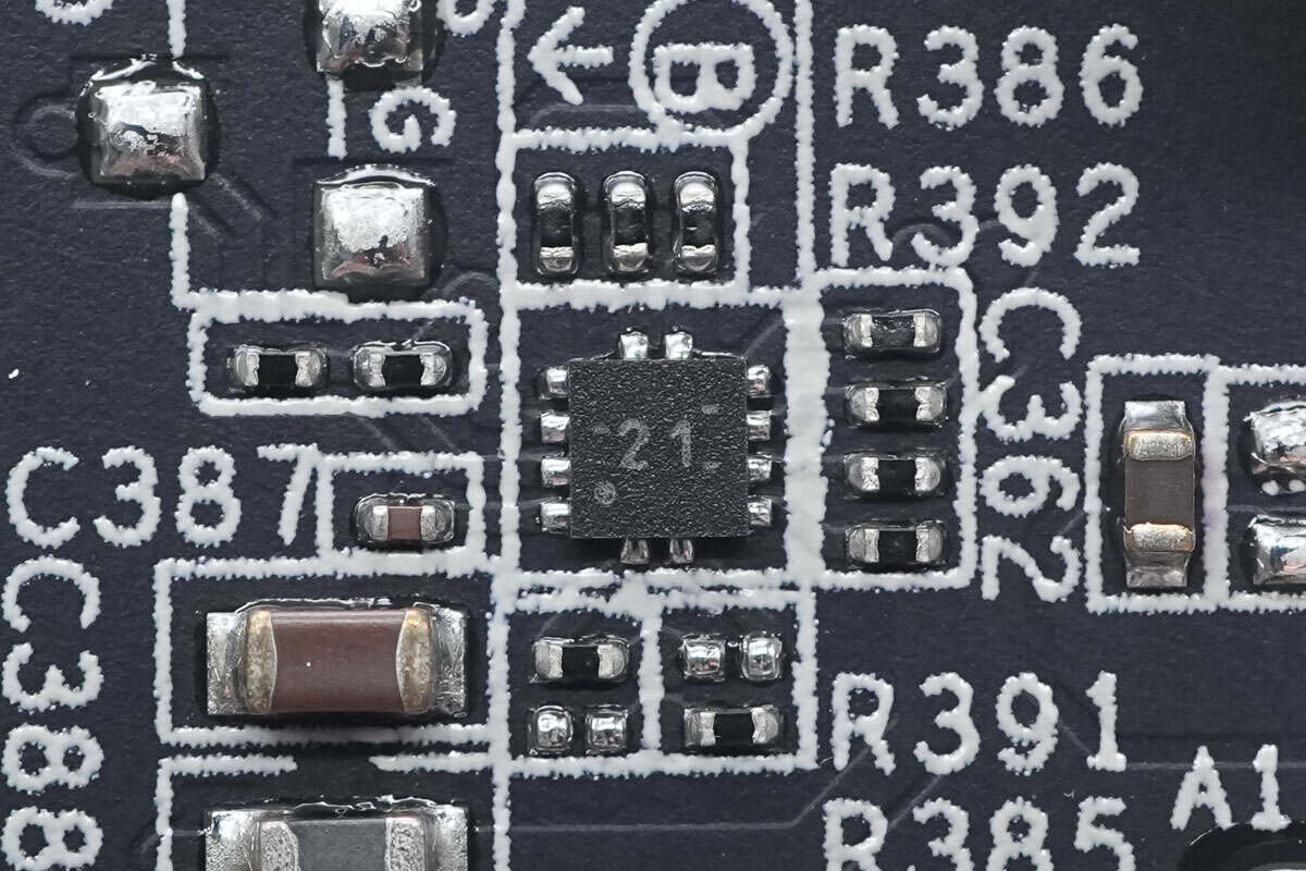
The USB-C interface controller is from Texas Instruments, marked with "21," model TUSB321. It is a USB Type-C configuration channel logic and port controller chip that supports VCONN, packaged in an X2QFN.
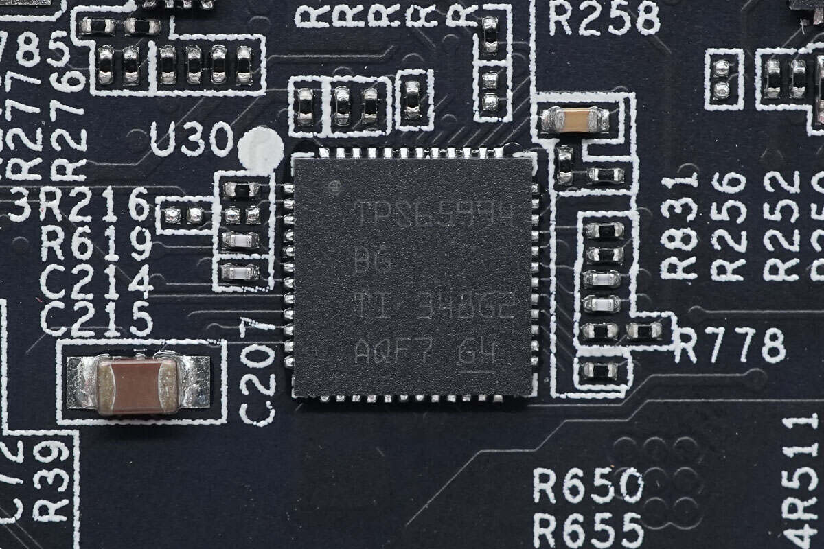
The USB-C interface controller is from Texas Instruments, marked TPS65994BG, and comes in a QFN48 package.
Close-up of the 10mΩ current sense resistor.
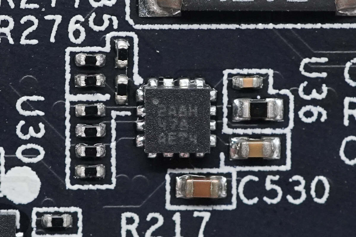
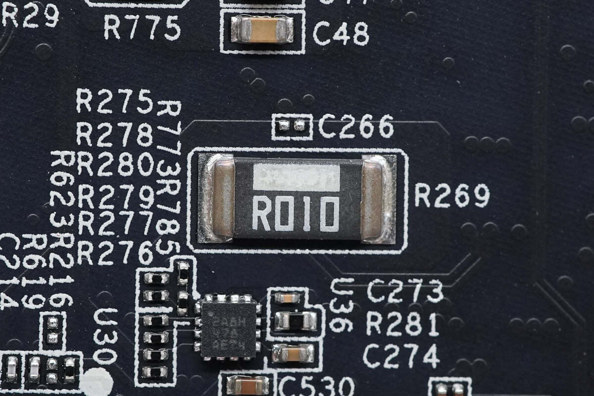
The overcurrent protection IC comes from Texas Instruments, marked 2ABH, model TPS259472. It supports up to 23V operating voltage and 6A current, with configurable overvoltage clamping and overcurrent protection thresholds. The chip features adjustable output slew-rate control, thermal shutdown protection, complies with IEC 62368-1 CB certification, and adopts a 2×2 mm QFN package.

Another USB-C port controller is the Texas Instruments TPS65994BG.

Close-up of the 10 mΩ current sense resistor.
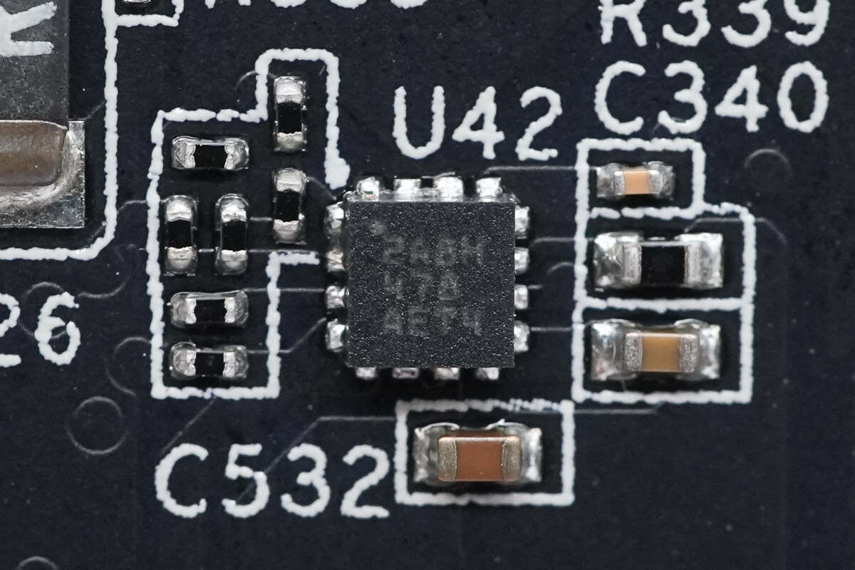
The overcurrent protection chip is the Texas Instruments TPS259472.
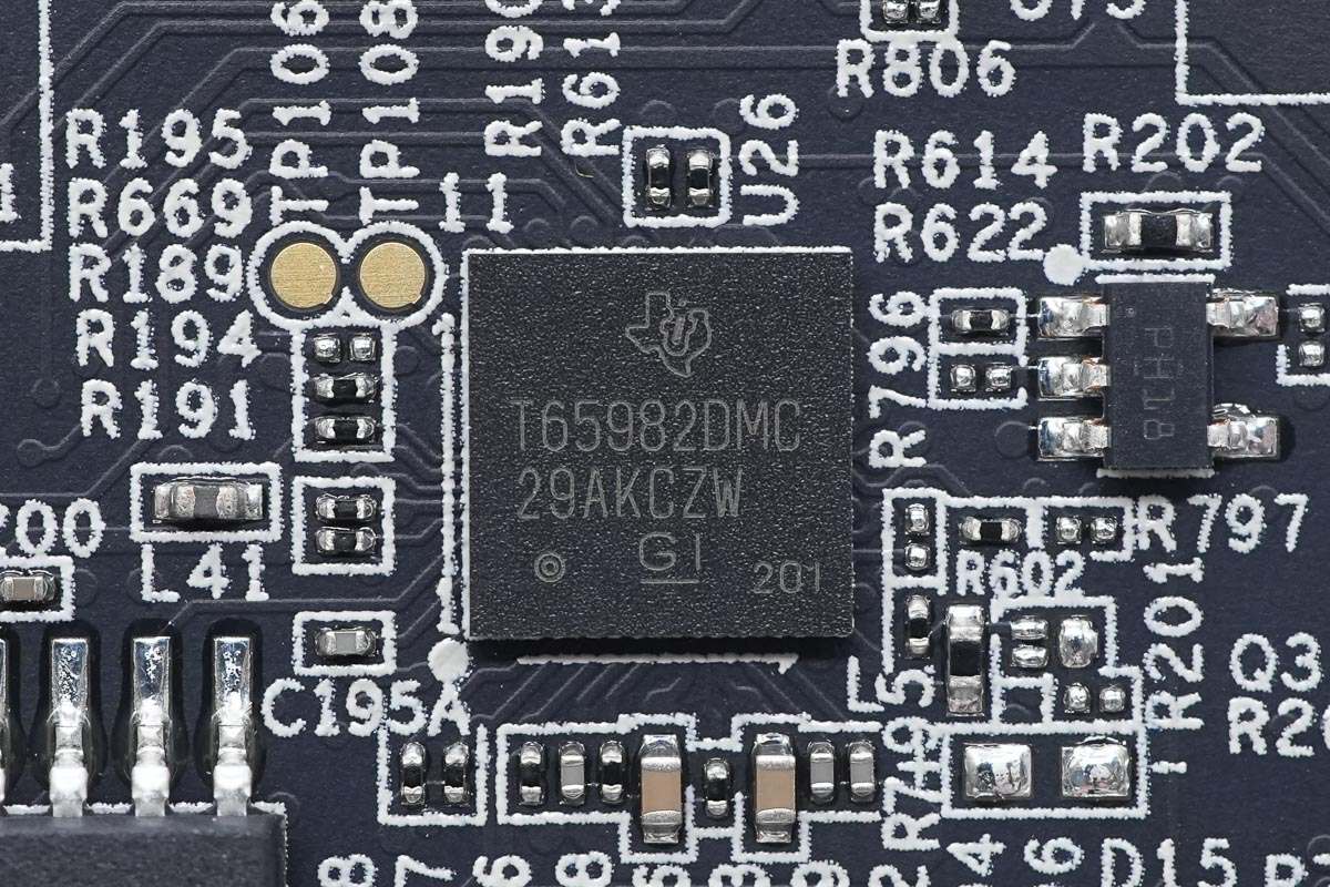
The USB-C management controller is the Texas Instruments TPS65982DMC, used for dock-side chip interface management. It communicates via the I2C bus, provides USB Billboard functionality, and comes in an NFBGA96 package.
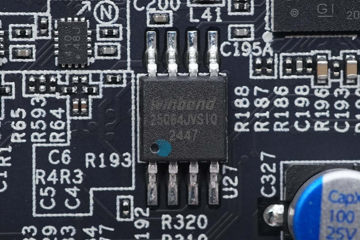
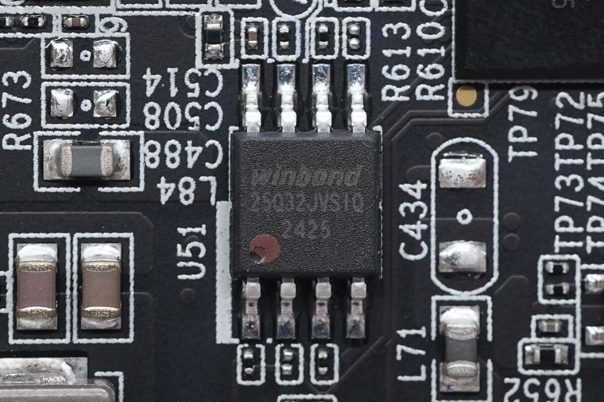
The memory chip is from Winbond, model W25Q64JVSSIQ, offering 8 MB capacity, supporting a 2.7–3.6 V operating voltage, and packaged in SOIC-8.

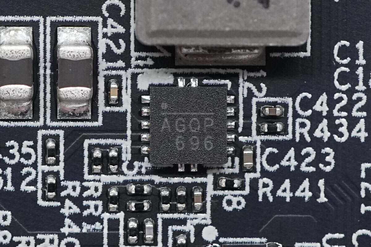
The synchronous buck converter is from MPS, marked AGQ, model MP2229. It supports a 4.5–21 V input range, integrates MOSFETs, delivers up to 6 A output current, features programmable switching frequency with external clock input support, and comes in a QFN-14 package.
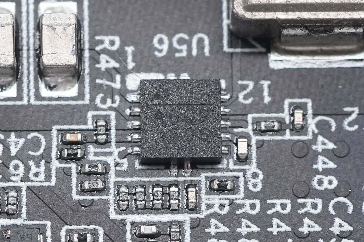
Another synchronous buck converter uses the same model.

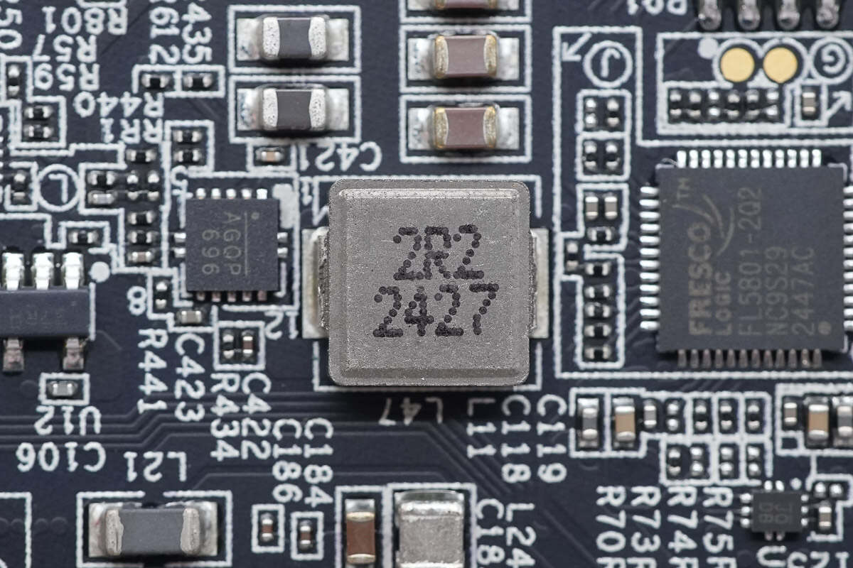
Close-up of the paired 2.2 μH alloy inductor.
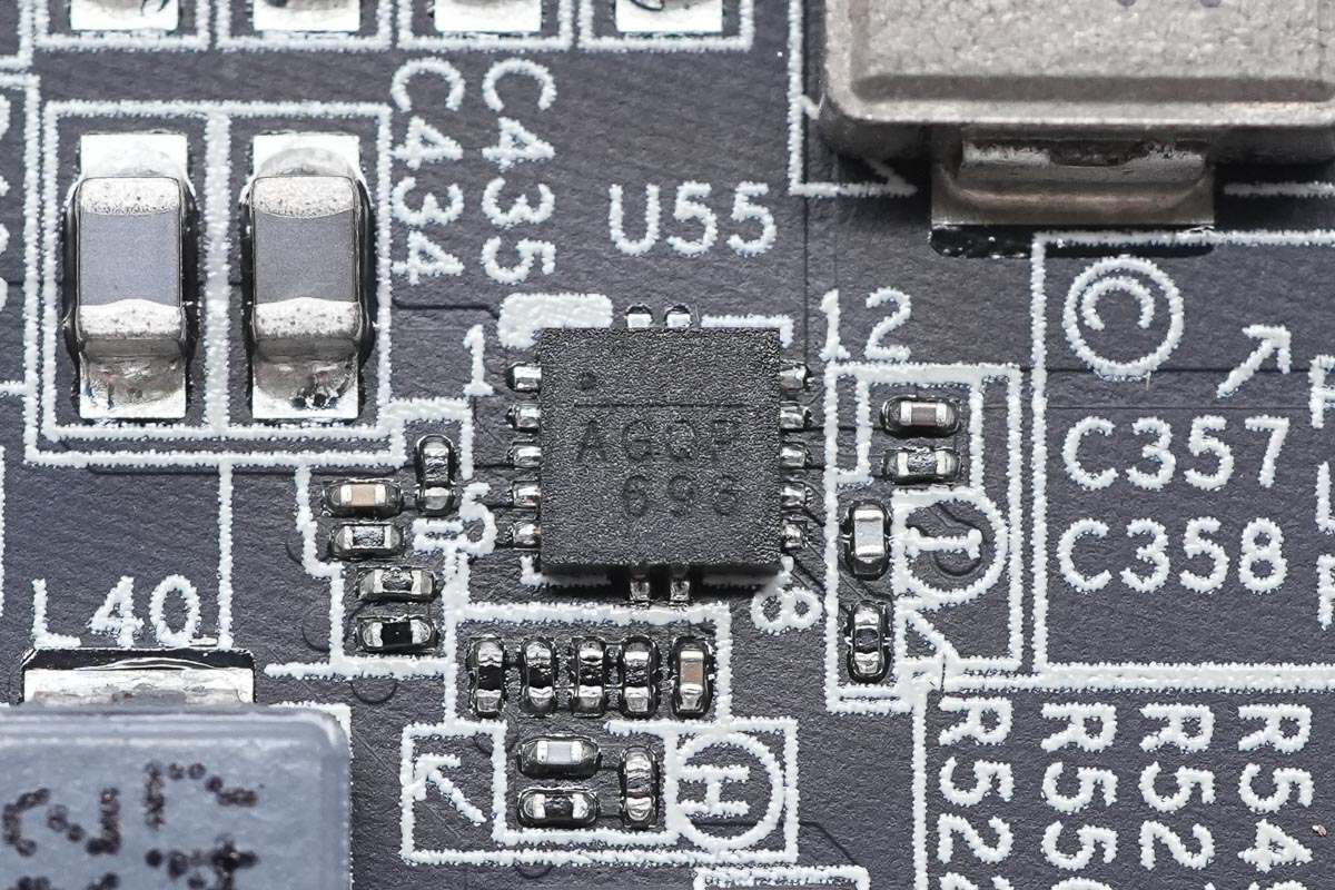
Close-up of the third MP2229 synchronous buck converter.
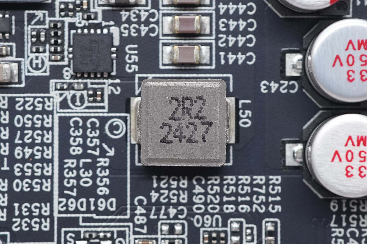
Close-up of its 2.2 μH alloy inductor.
The Thunderbolt 5 PCB uses a total of four MP2229 synchronous buck converters.
Close-up of the 2.2 μH alloy inductor.
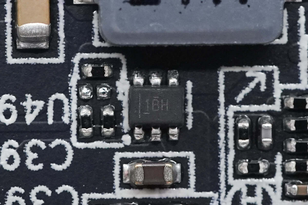
The synchronous buck converter is from Texas Instruments, marked 1BH, model TLV62569A. It integrates MOSFETs, supports a 2.5–5.5 V input range, allows 100% duty cycle, operates at 1.5 MHz switching frequency, and comes in a SOT563 package.

Close-up of the 2.2 μH alloy inductor.
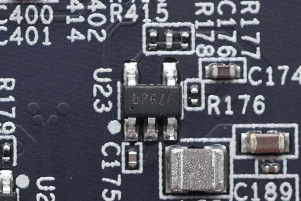
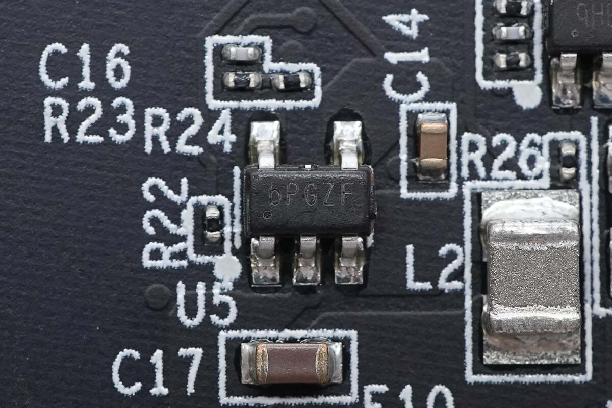
The synchronous buck converter is from Silergy, marked bP, model SY8088I. It integrates MOSFETs, supports a 2.5–5.5 V input range, delivers 1 A output current, allows 100% duty cycle, operates at 1.5 MHz switching frequency, and comes in a SOT23-5 package.
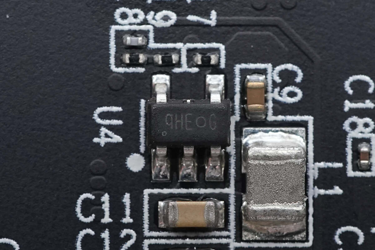
The synchronous buck converter is from Silergy, marked qH, model SY8089A1. It integrates MOSFETs, supports a 2.5–5.5 V input range, delivers 2 A output current, allows 100% duty cycle, operates at 1.5 MHz switching frequency, and comes in a SOT23-5 package.

The current-sensing IC is from Texas Instruments, model INA219. It is a zero-drift, bidirectional current and power monitor with an I²C interface, supporting up to 26 V, featuring voltage and current measurement channels, and comes in a SOT23-8 package.
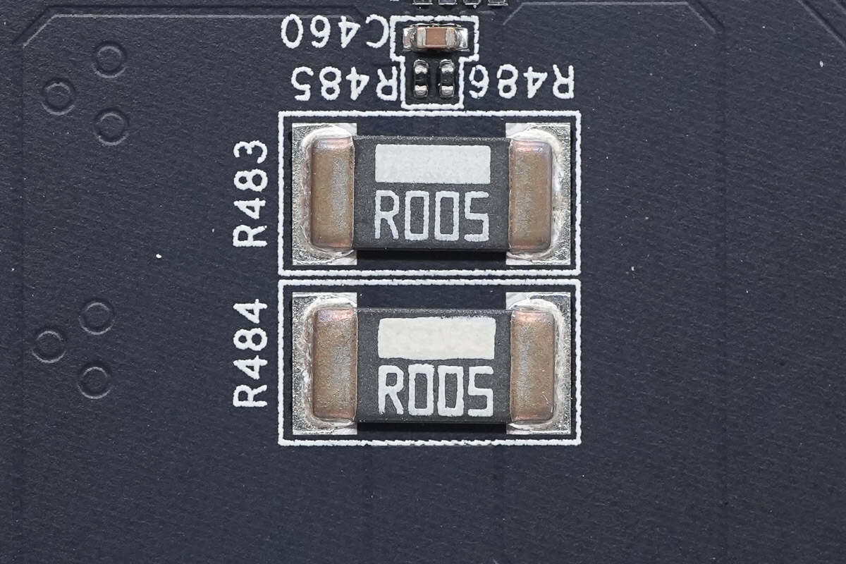
Two 5 mΩ resistors are used for current sensing.
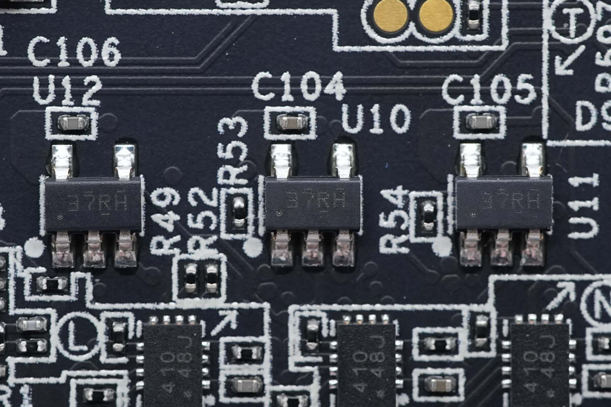
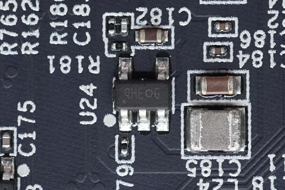
Three buffer ICs are from Texas Instruments, marked 37RH, model SN74LV1T125. They feature tri-state outputs and come in SOT23 packages.
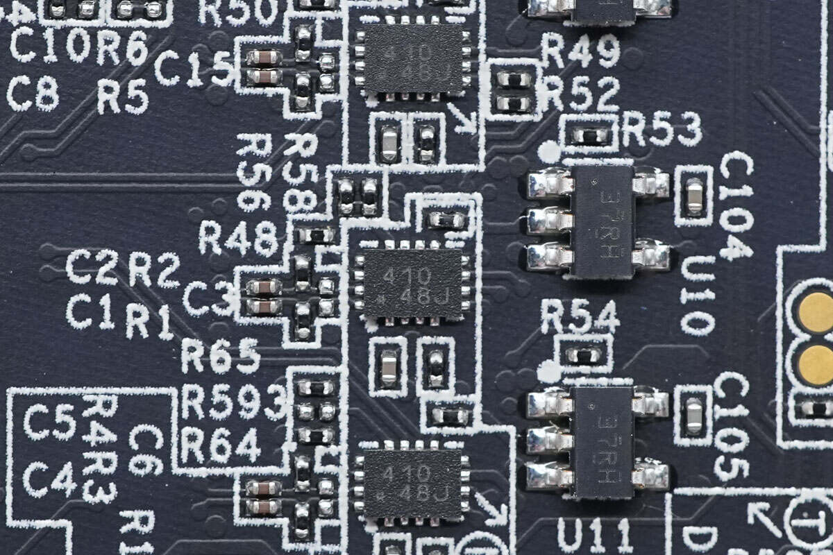
The multiplexer IC is from Texas Instruments, marked 410, model TS3USBCA410. It handles analog audio, DP AUX, PCIe differential clocks, or other general-purpose differential or single-ended signal multiplexing. It features three inputs, supports both pin and I²C configuration, offers 500 MHz bandwidth, operates over a 2.4–5.5 V wide voltage range, and comes in a UQFN16 package.
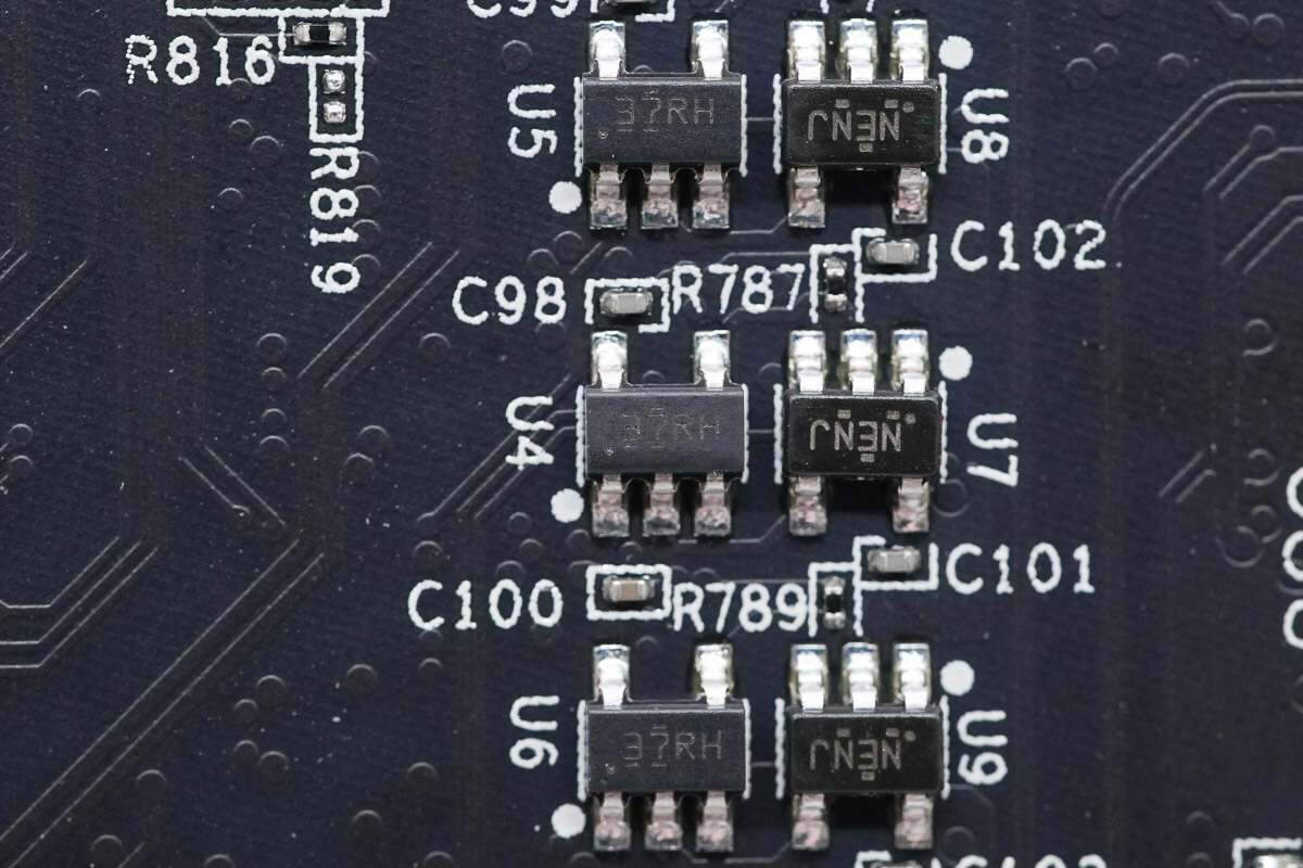
Three buffer ICs use the Texas Instruments SN74LV1T125.
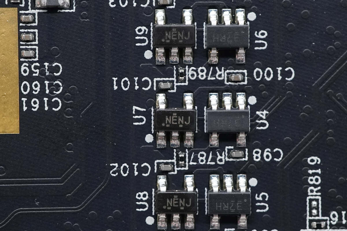
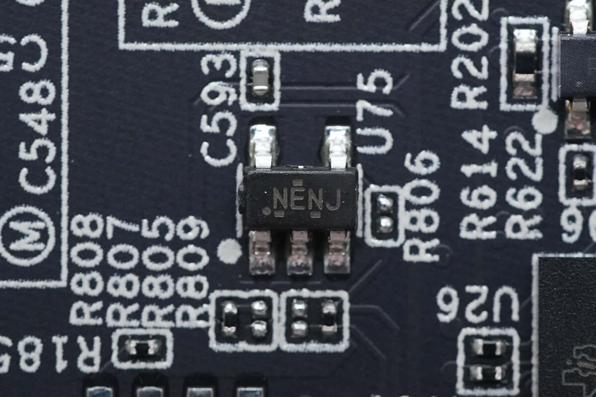
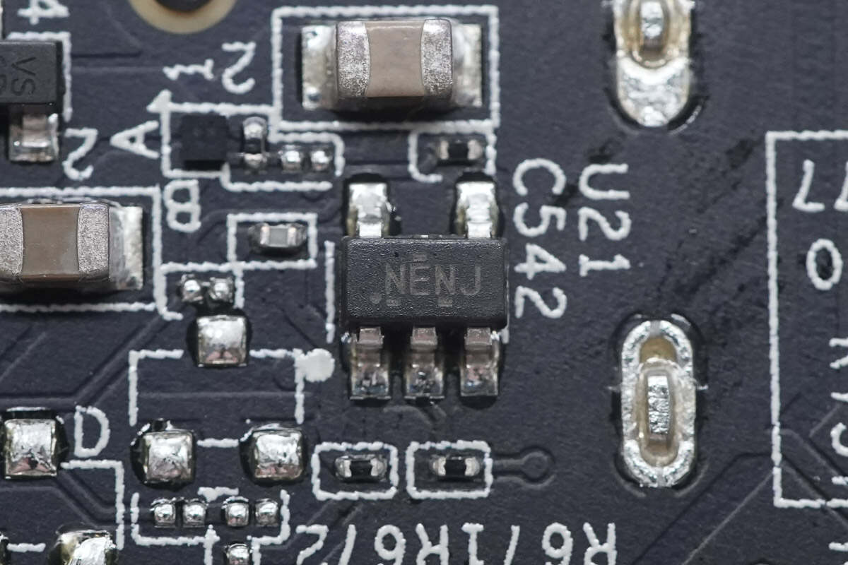
Three buffer ICs are from Texas Instruments, marked NENJ, model SN74LV1T126. They feature tri-state outputs and come in SOT23 packages.
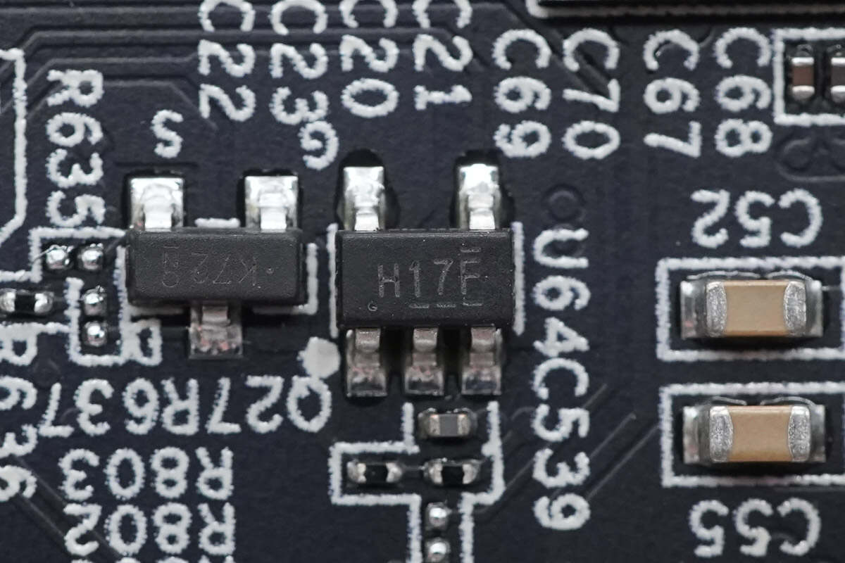
The buffer is from Texas Instruments, marked H17F, model SN74AUP1G17. It is a single low-power buffer with a Schmitt-trigger input and comes in a SOT23 package.
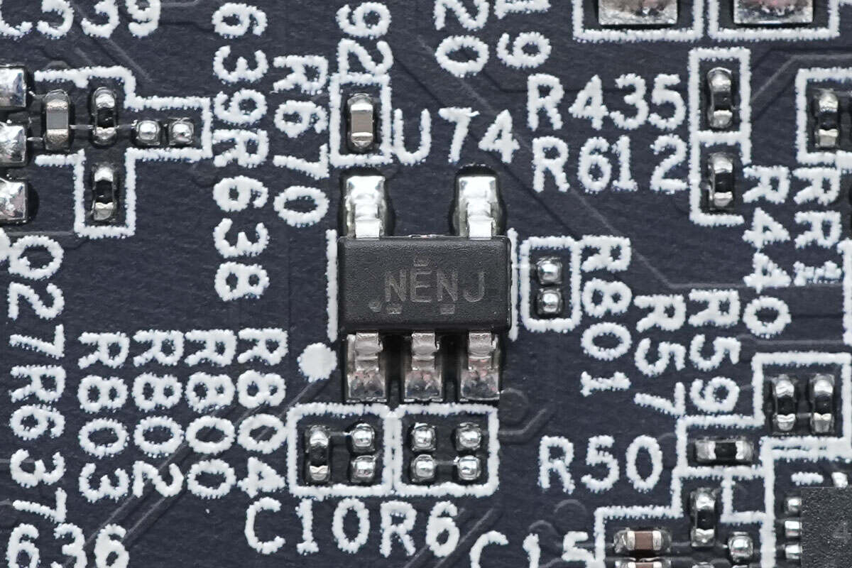
The buffer IC uses the Texas Instruments SN74LV1T126.
The buffer IC uses Texas Instruments SN74LV1T126.
The buffer IC is Texas Instruments SN74LV1T126.
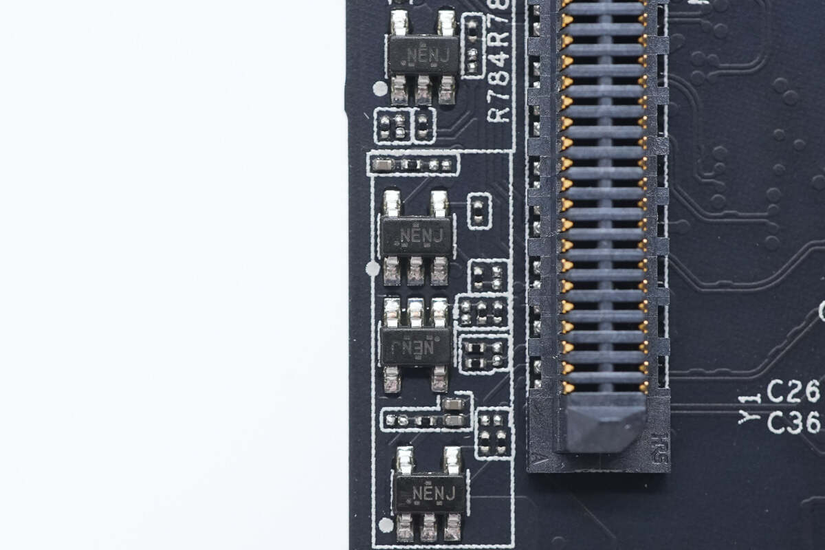
Four buffer ICs use Texas Instruments SN74LV1T126.
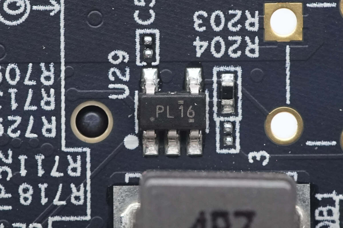
The voltage supervisor is from Texas Instruments, marked PL16, model TPS3840PL16. It is a micro-power input voltage monitor with manual reset and programmable reset delay, packaged in SOT23.
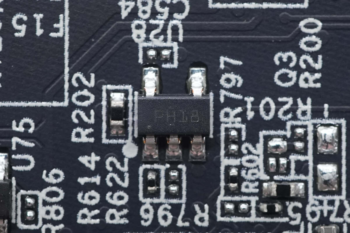
Another voltage supervisor is marked PH18.
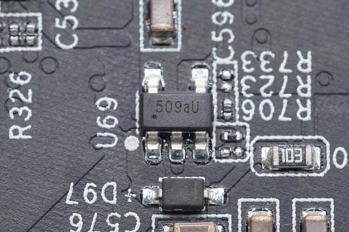
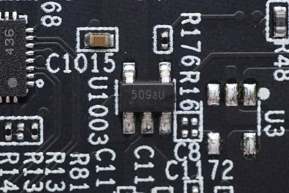
The overcurrent protection IC is model G509 and comes in a SOT23 package.

The switch is from DIODES, marked JQ, model PI3USB102E. It is a USB 2.0 switch supporting high-, full-, and low-speed applications, with overvoltage protection, and comes in a TQFN10 package.
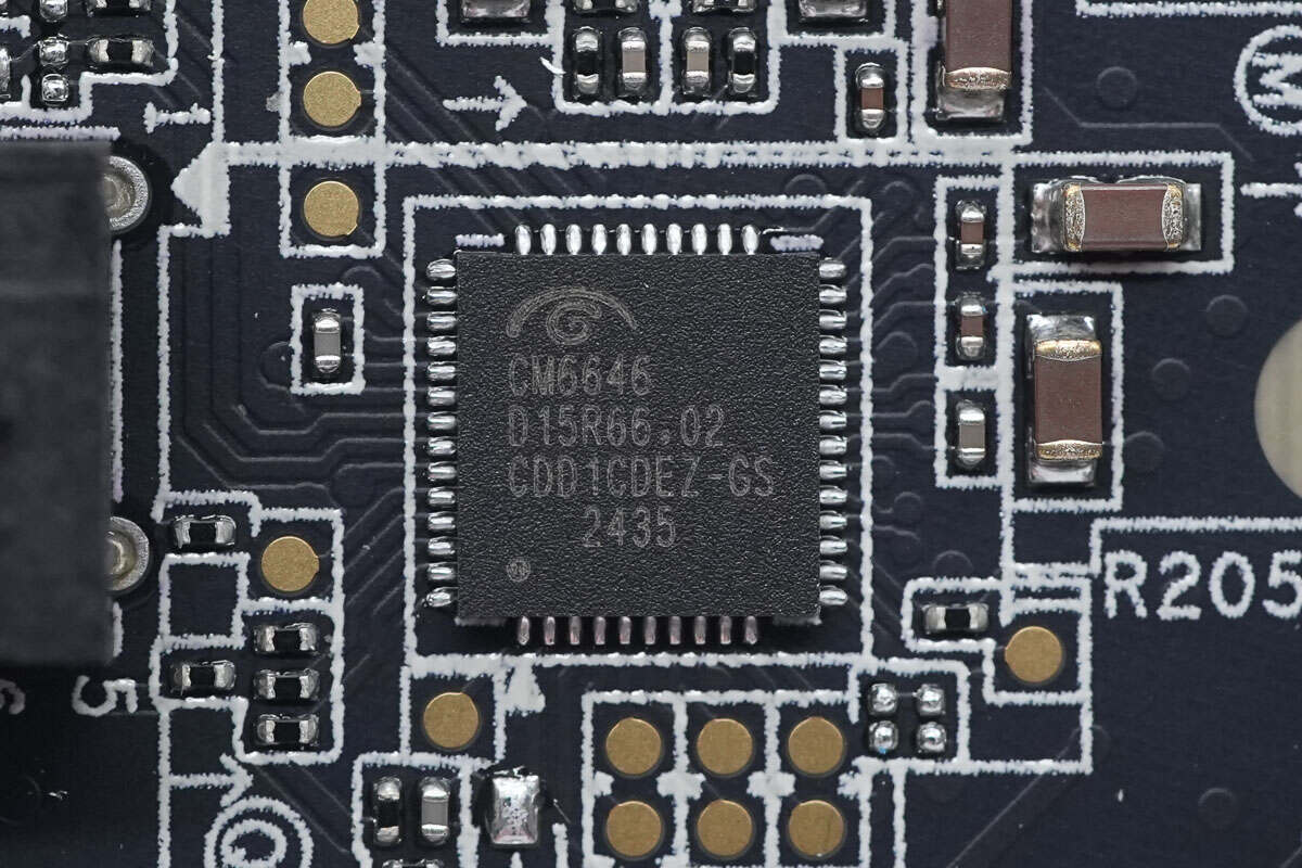
The audio IC is from Cmedia, model CM6646. It is a USB 2.0 high-speed audio codec with 2-channel DAC and 2-channel ADC, suitable for headphones, microphones, and similar applications, and comes in a QFN-48 package.
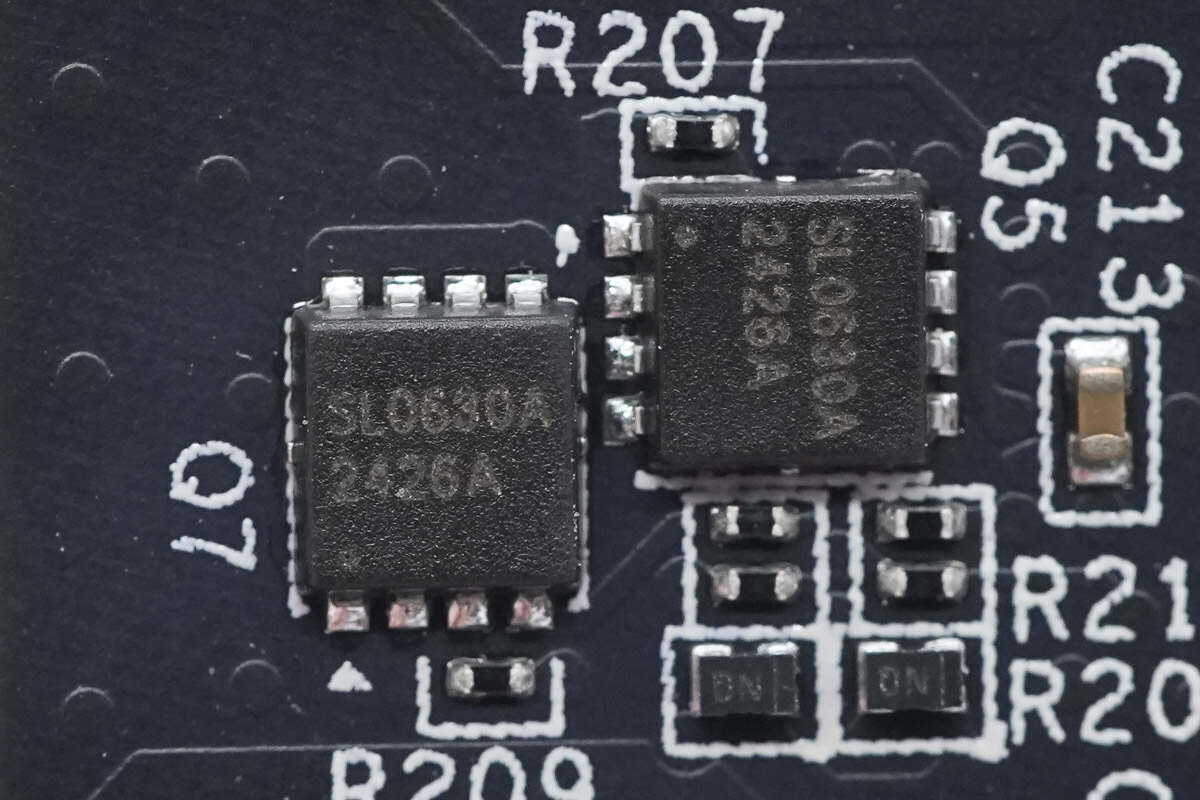
The VBUS MOSFET is from JJM, model JMSL0630AU. It is an NMOS with a 60 V voltage rating, 22 mΩ on-resistance, and comes in a 3×3 mm 8L PDFN package.
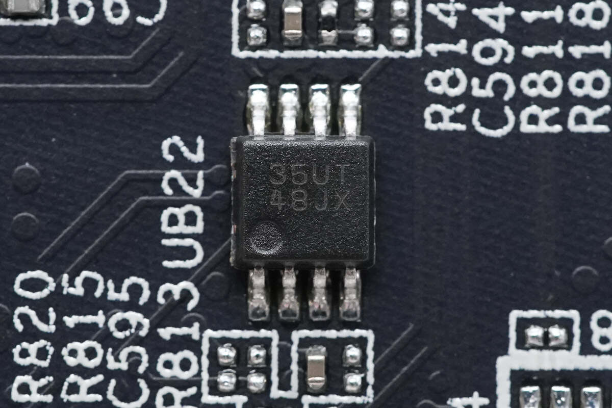
The level shifter is from Texas Instruments, marked 35UT, model TXS0102. It is a 2-bit bidirectional voltage-level translator suitable for open-drain and push-pull applications. The A port supports 1.65–3.6 V, the B port supports 2.3–5.5 V, and it comes in an SSOP package.
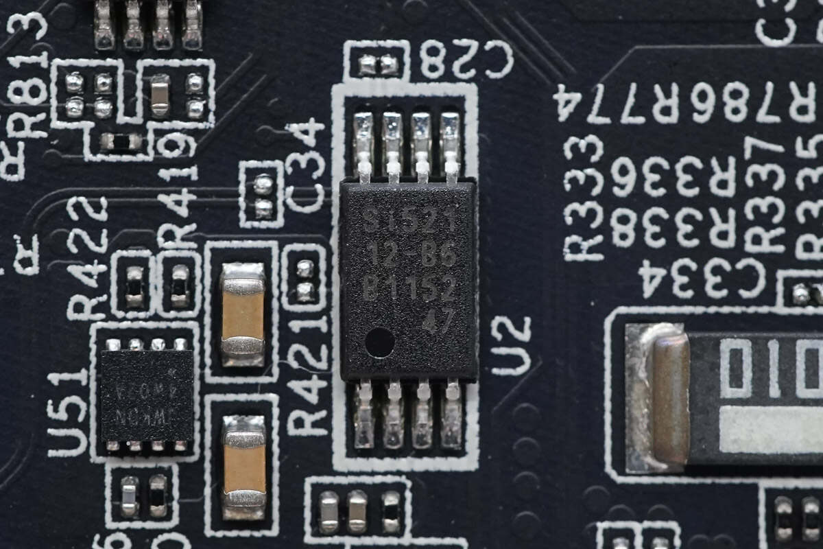
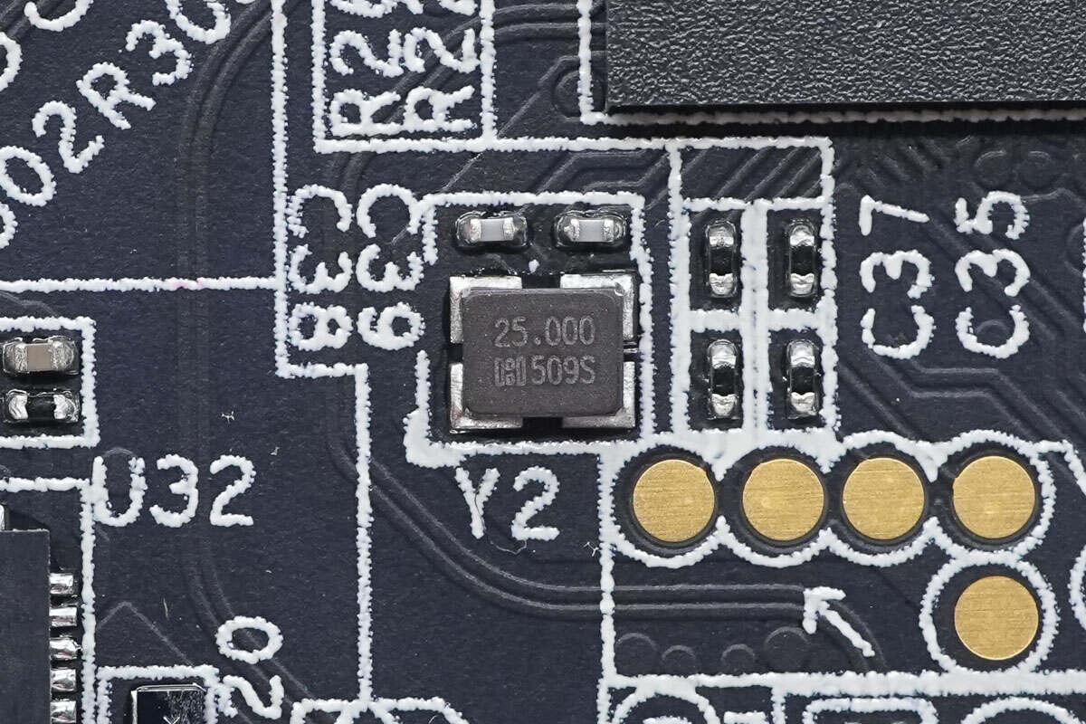
The clock generator is from SKYWORKS, model Si52112-B6. It is a dual-output PCIe 3 clock generator, backward compatible with PCIe 1 and 2 general clocks, using a 25 MHz crystal or clock input, and comes in an 8-pin TSSOP package.
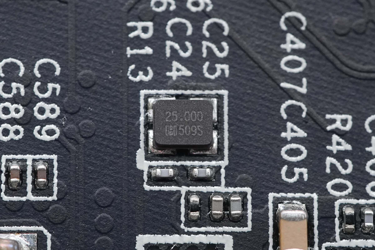
Close-up of the 25.000 MHz clock crystal.
The load switch is from JOULWATT, marked JWKD, model JW7106. It is a single-channel switch with 5.5 V operating voltage and 6 A current, featuring programmable rise time, fast output discharge, and thermal protection, packaged in a 2×2 mm DFN-8.
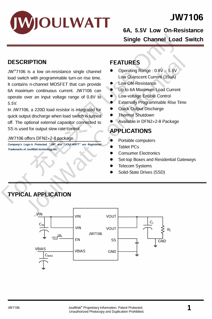
Here is the information about JOULWATT JW7106.
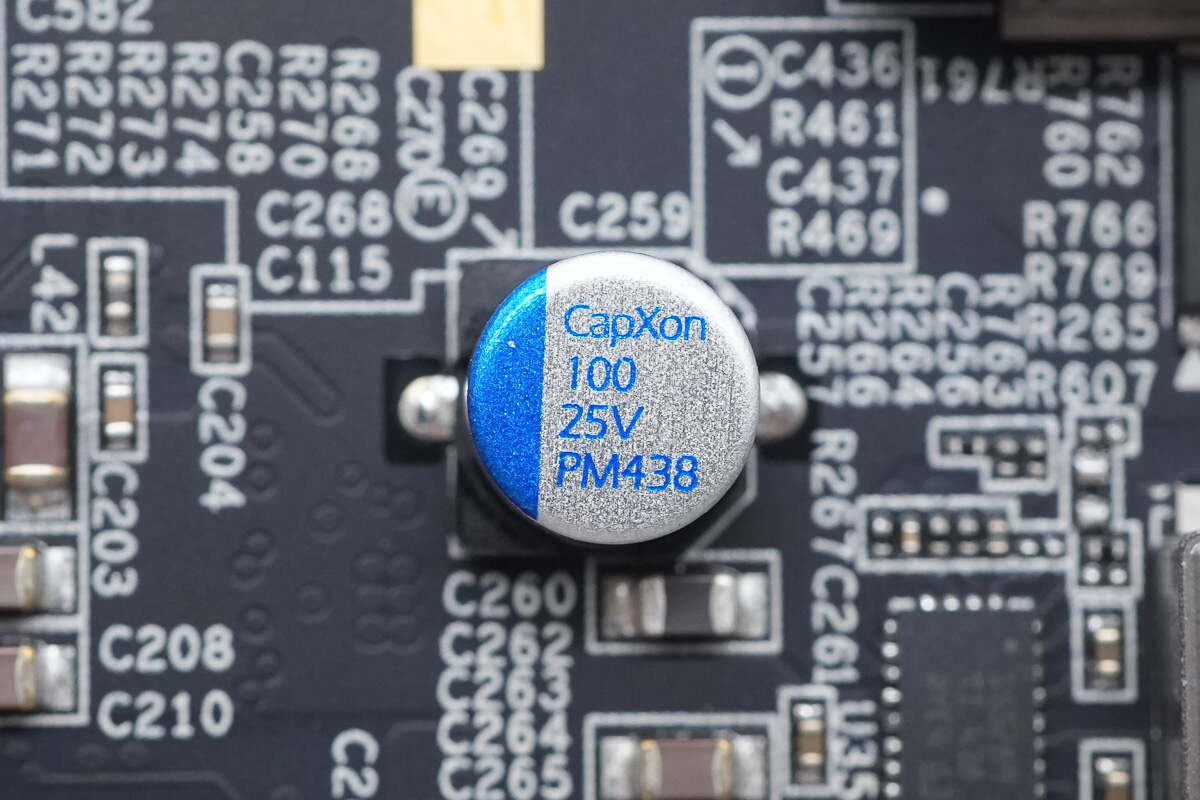
The filter capacitor is from CapXon, a PM-series solid capacitor, rated 100 μF, 25 V.
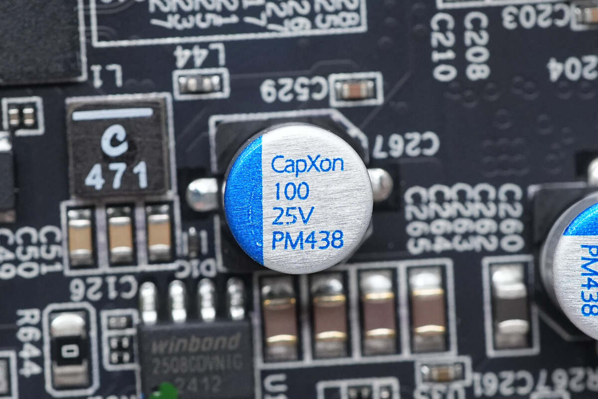
Another capacitor with the same specifications.

The other two filter capacitors have the same specifications.
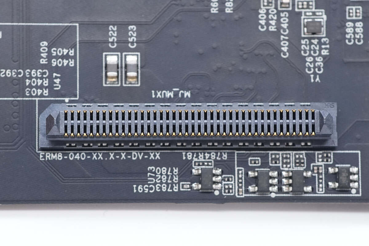
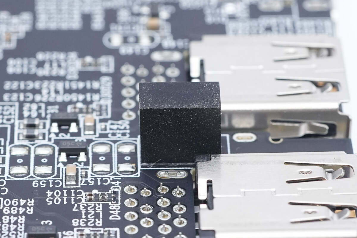
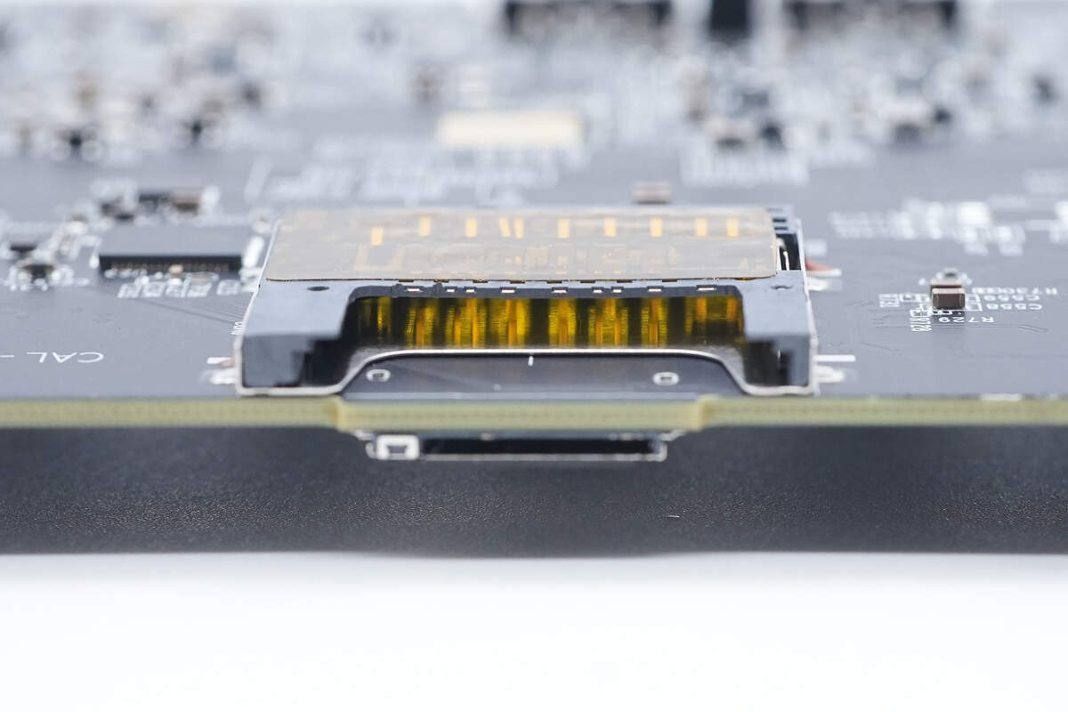
Close-up of the high-speed precision connector linking the two PCBs.
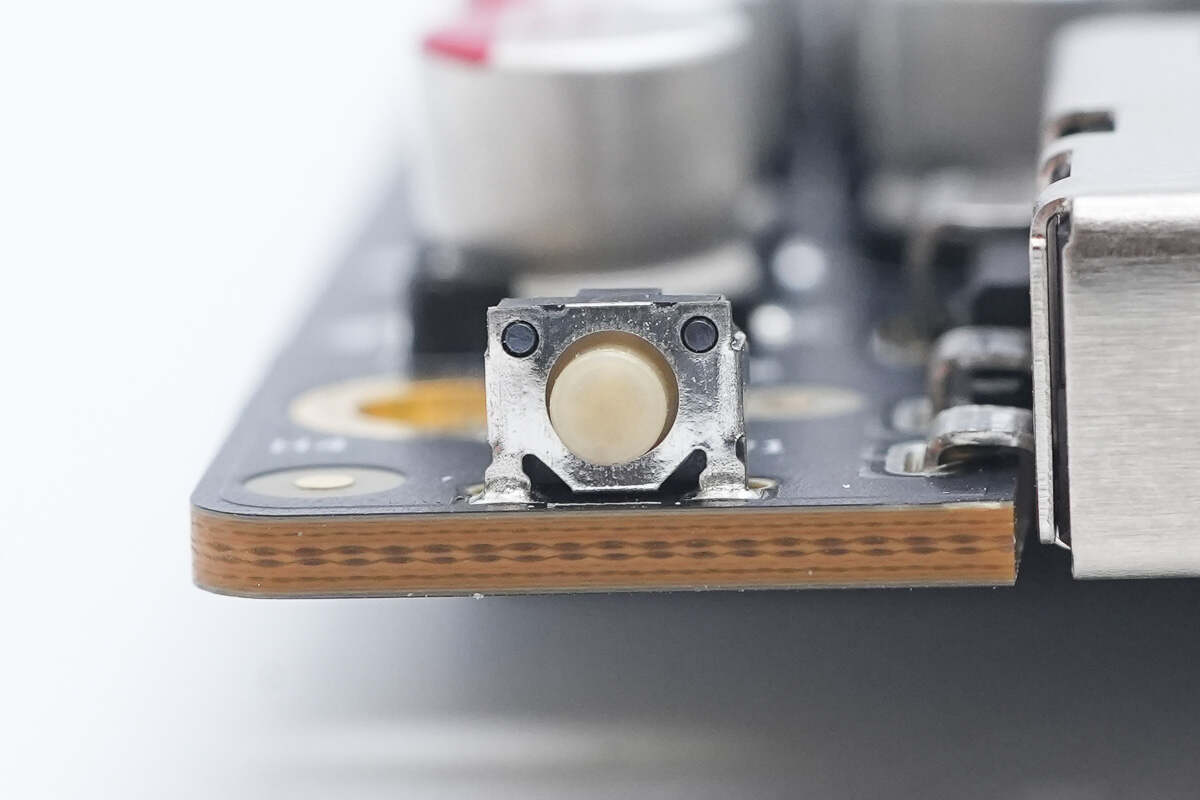
Close-up of the reset button.
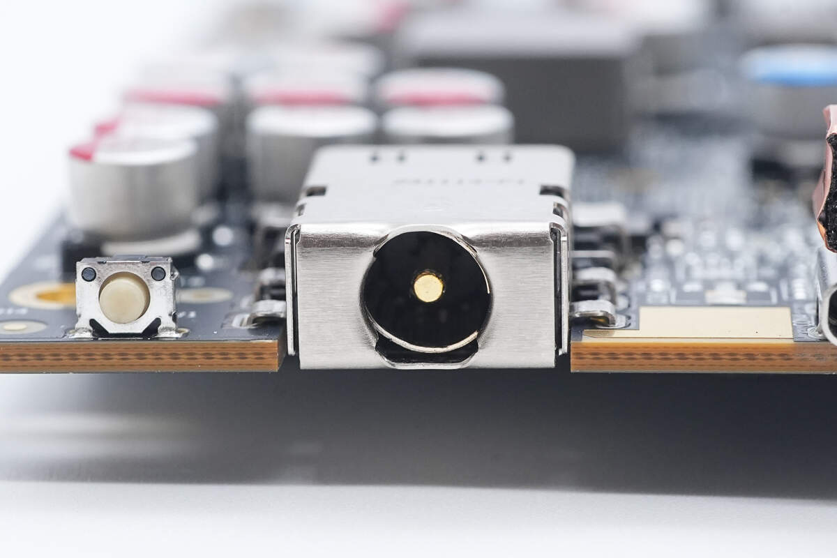
Close-up of the DC input port.
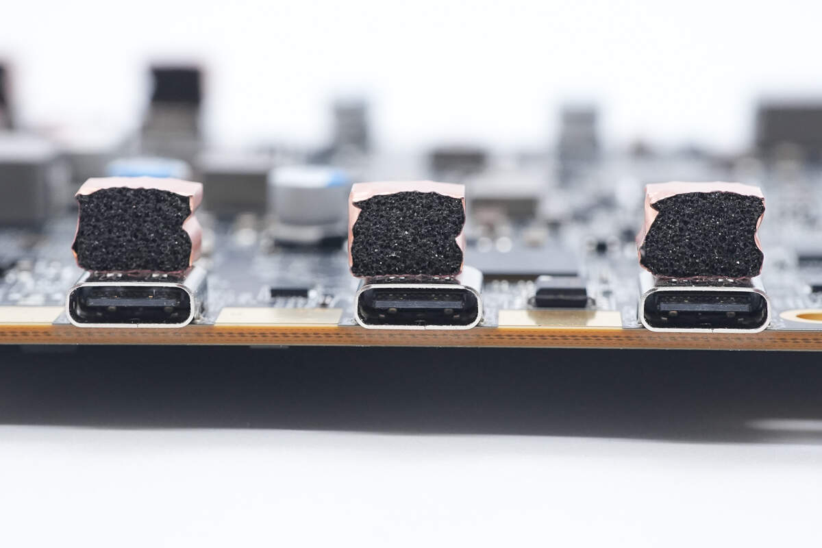
Close-up of the USB-C port via soldering, with copper tape on the casing for grounding.

Close-up of the DP port via soldering, with conductive fabric on the casing for grounding.
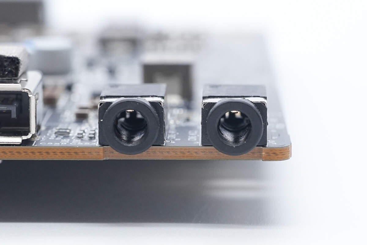
Close-up of the 3.5 mm audio jack via soldering for secure mounting.
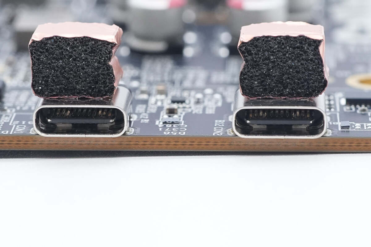
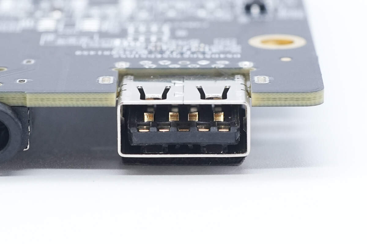
Close-up of the front-panel USB-C port soldered through vias for secure mounting, with copper tape on the casing for grounding.
Close-up of the LED indicator.
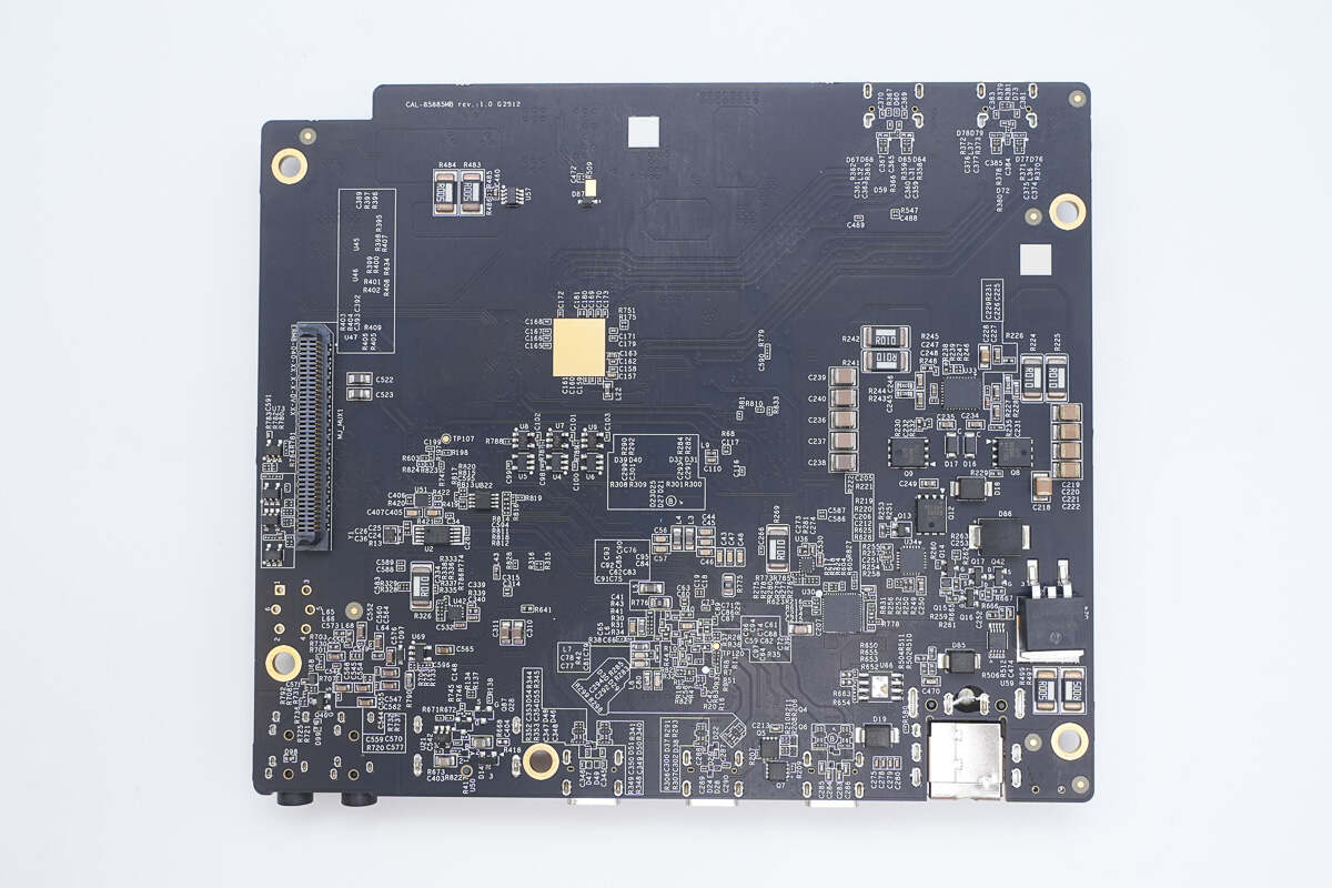
The interface expansion PCB includes a PCIe-to-USB controller, a USB hub chip, a switch, a 10 GbE network chip, and an audio chip.
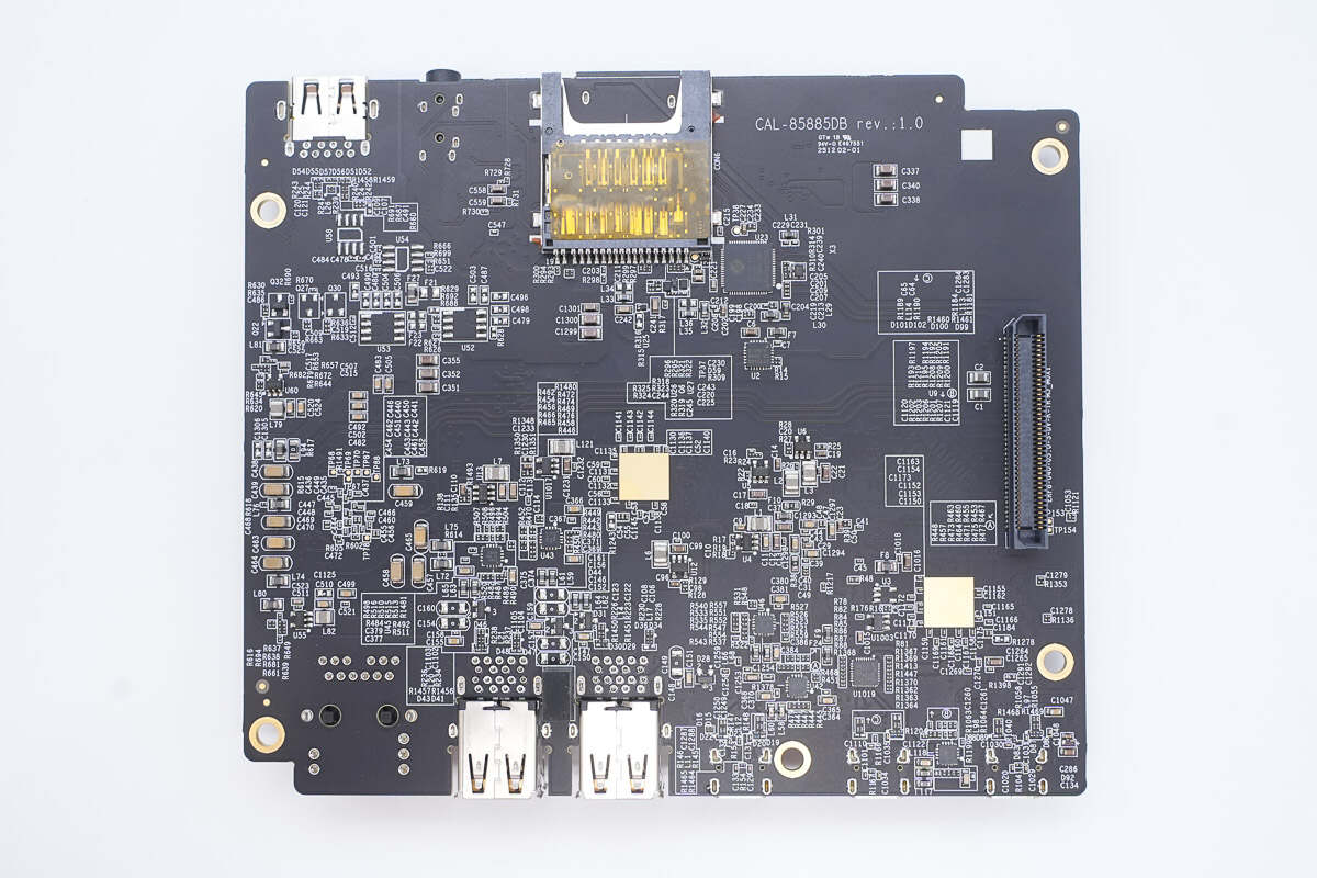
The other side features a card reader chip, a clock generator, and a switch.
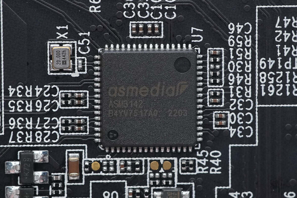
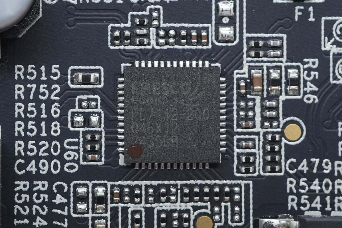
The USB bridge chip is from ASMedia, model ASM3142. It converts a PCIe Gen3 ×2 interface to USB 3.1 and comes in a QFN64 package.
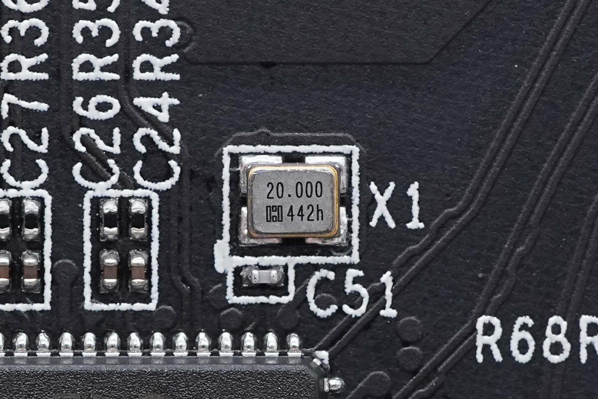
Close-up of the 20.000 MHz clock crystal.
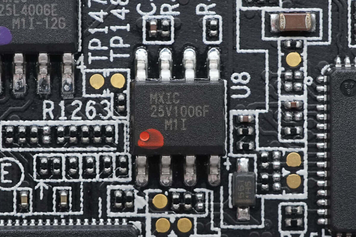
The memory chip is from MXIC, model MX25V1006F. It offers 128 KB capacity, supports a 2.3–3.6 V operating voltage, and comes in an SOP8 package.
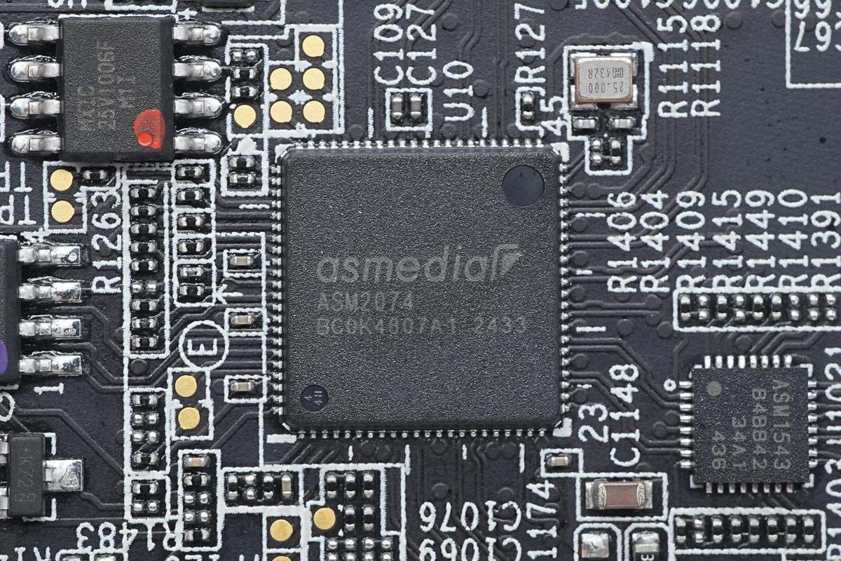
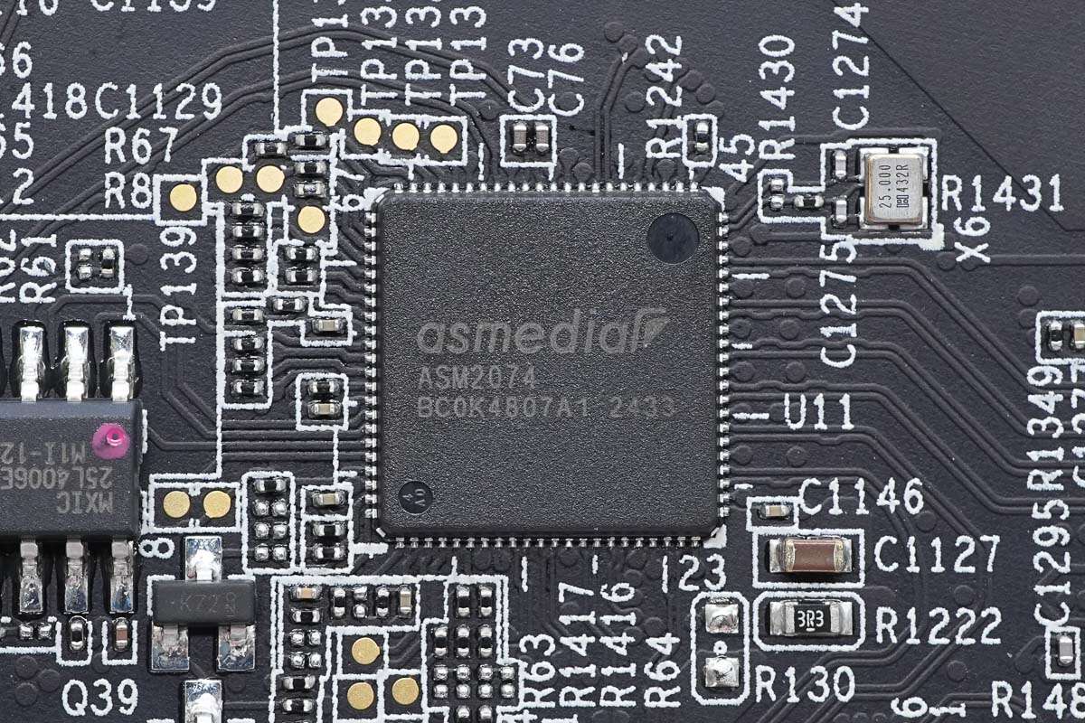
The USB hub is from ASMedia, model ASM2074. It supports USB 3.2 Gen1 at 10 Gbps, features four downstream ports, integrates an internal LDO, comes in a QFN88 package, and is used to expand three USB-C ports and one USB-A port.
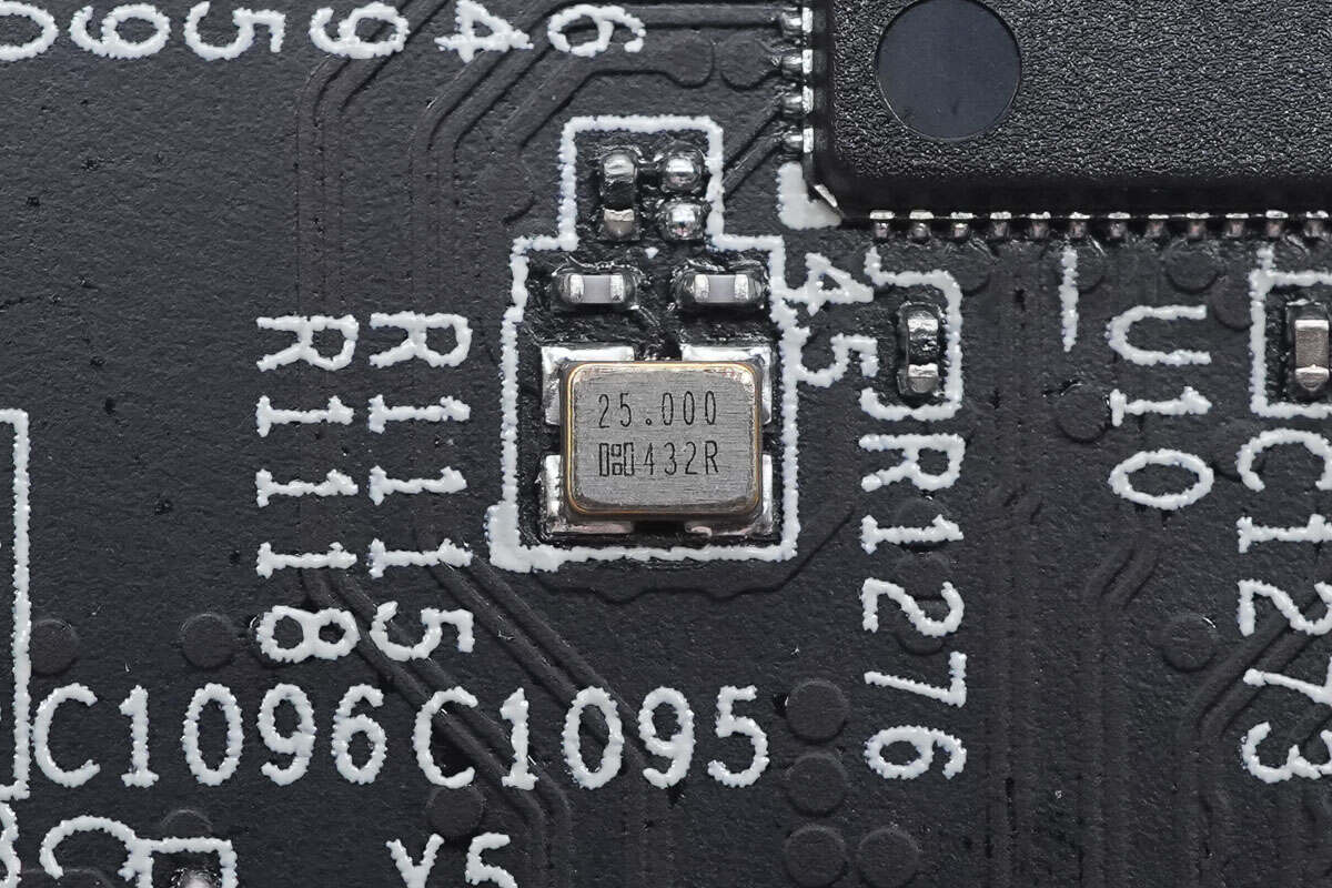
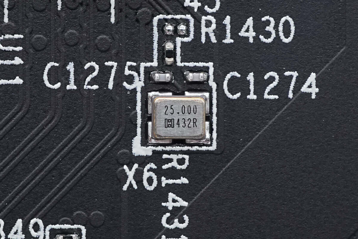
Close-up of the 25.000 MHz clock crystal.
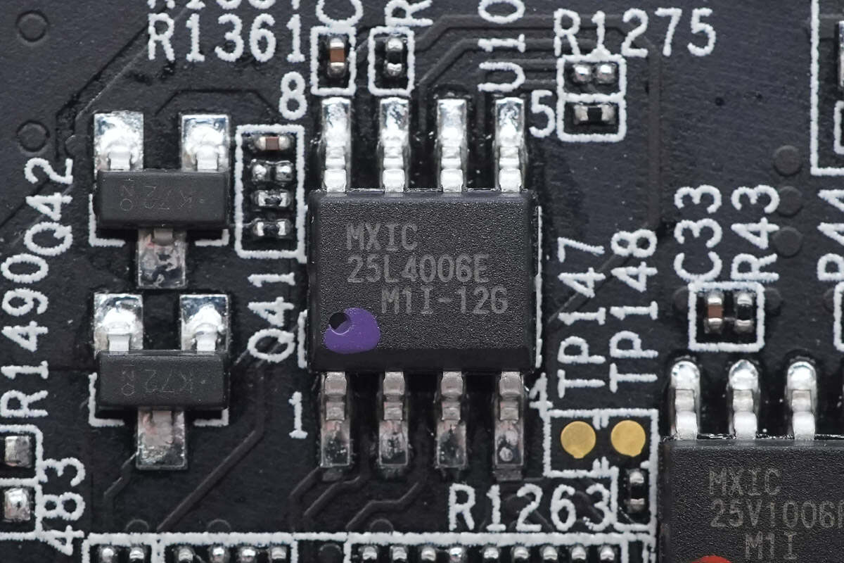
The memory chip is from MXIC, model MX25L4006E.
Another ASMedia ASM2074 hub is used to expand four USB-A ports.
Close-up of the 25.000 MHz clock crystal.

The memory chip is from MXIC, model MX25L4006E.

The ASMedia ASM1543 multiplexer switch is used for USB-C plug orientation switching, supports 10 Gbps transfer rates, and comes in a QFN32 package.
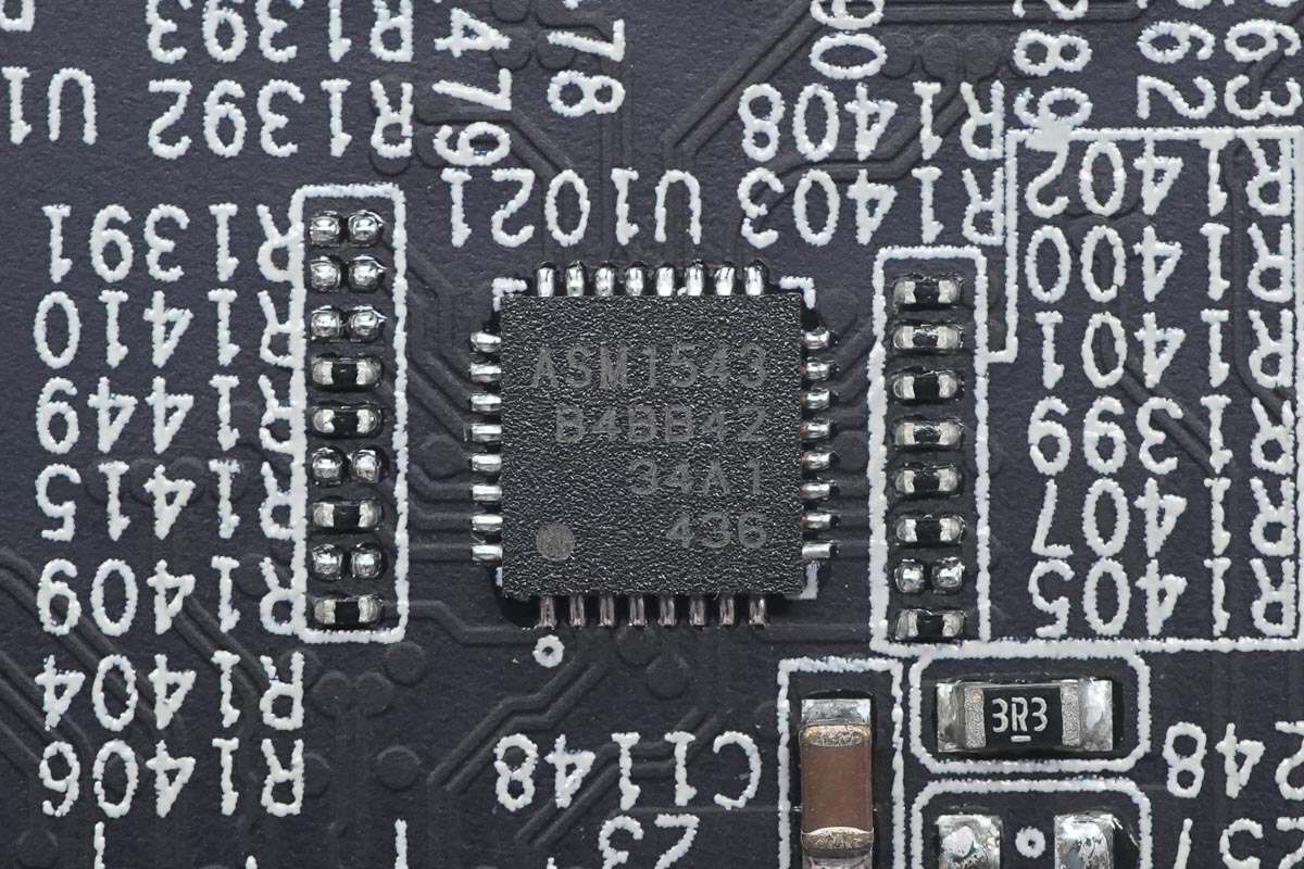
A total of three are used for the three USB-C ports.

Close-up of the third multiplexer switch.
The load switch for the USB-C ports is from Texas Instruments, model TPS2546.
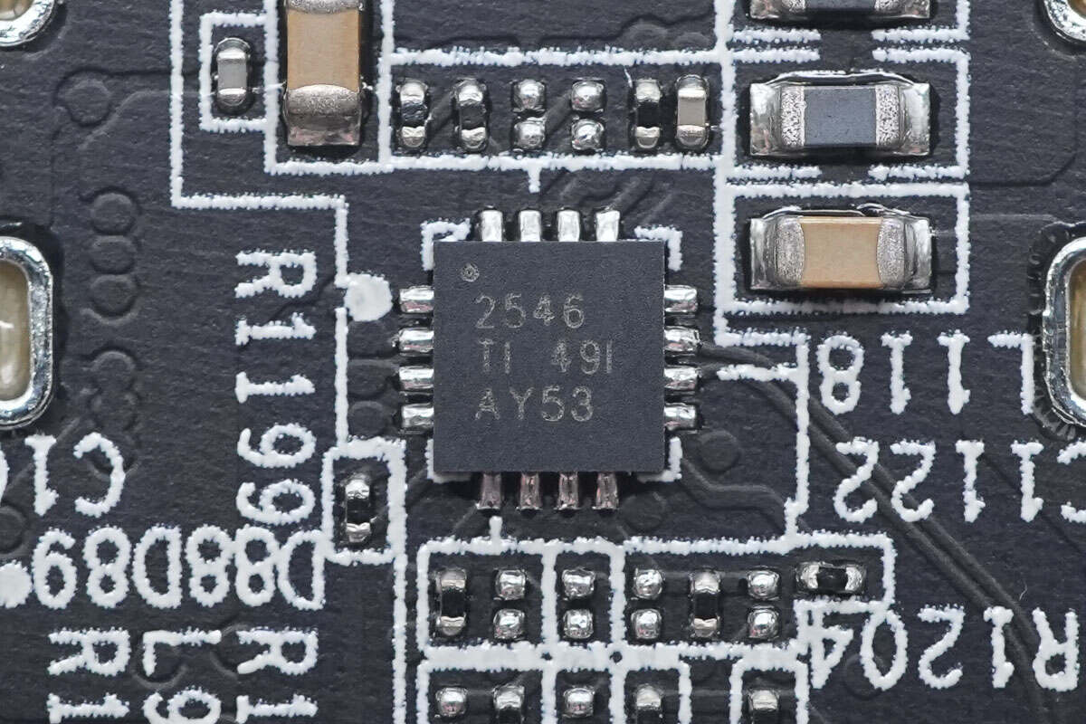
A total of three are used, corresponding to the three rear USB-C ports.
Close-up of the third TPS2546 load switch.
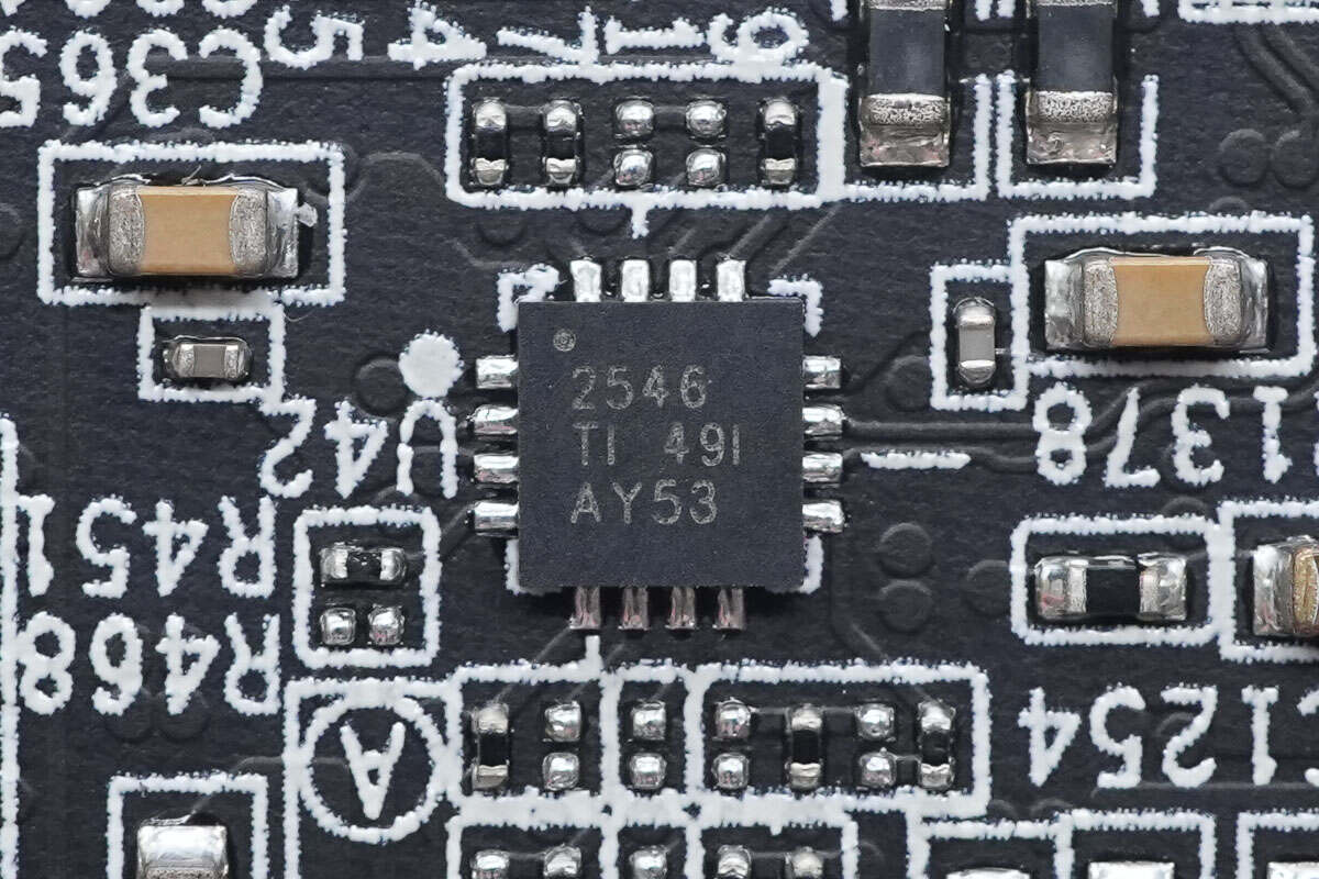
The four rear USB-A ports also use TPS2546 load switches.
Close-up of the second TPS2546 load switch.
Close-up of the third TPS2546 load switch.
Close-up of the fourth TPS2546 load switch.
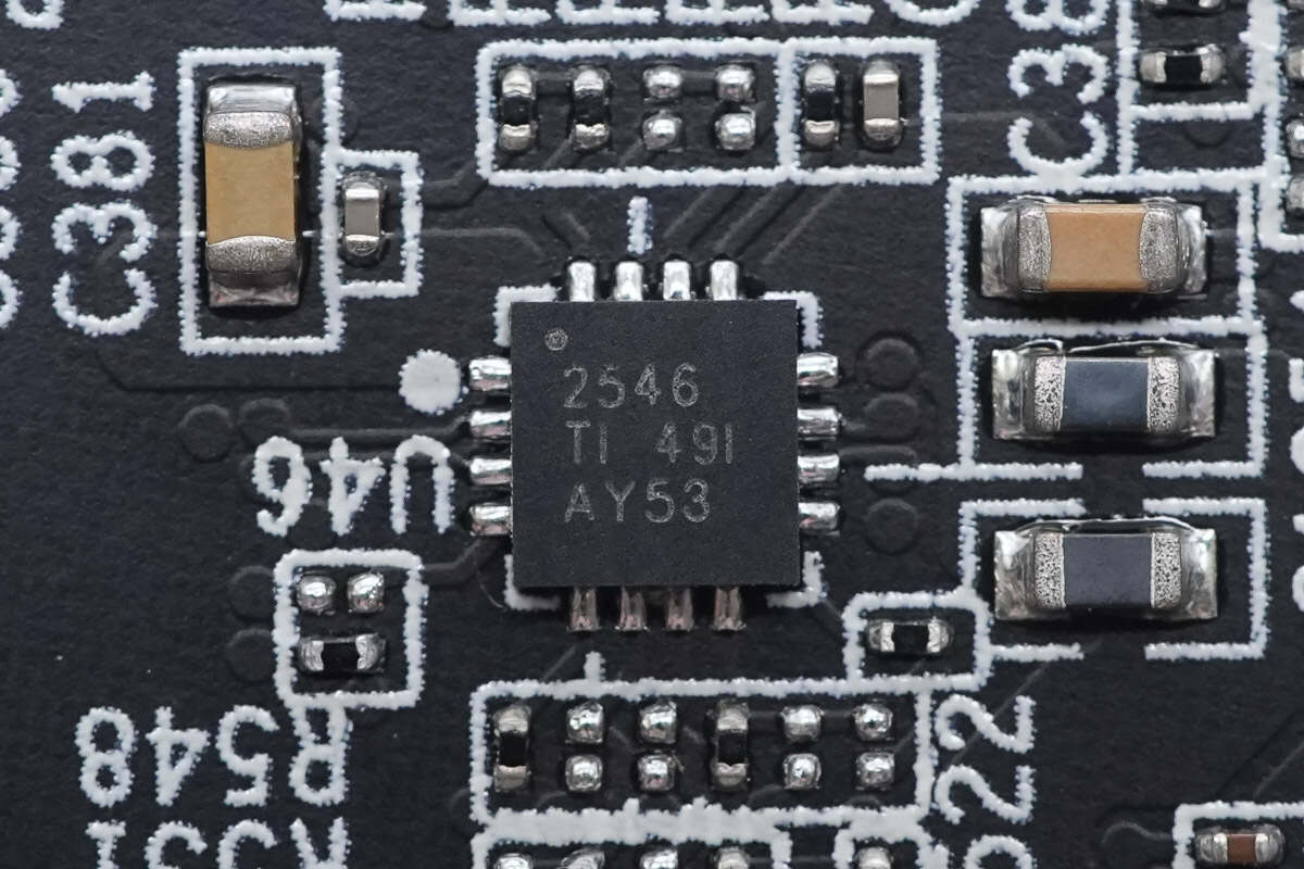
The front-panel USB-A port also uses a TPS2546 load switch.
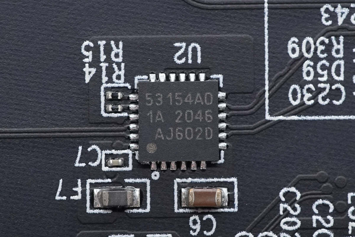
The PCIe clock buffer is from SKYWORKS, model Si53154. It provides four PCIe clock outputs, four hardware enable inputs, supports I²C communication control, and comes in a 24-pin QFN package.
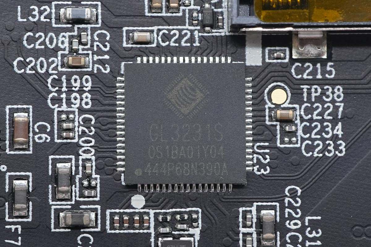
The card reader chip is from GENESYS, model GL3231S. It is a USB 3.1 Gen1 card reader controller with an integrated DC-DC converter, supporting SD 3.0 UHS‑I and SD 4.0 UHS‑II memory cards, and comes in a QFN64 package.
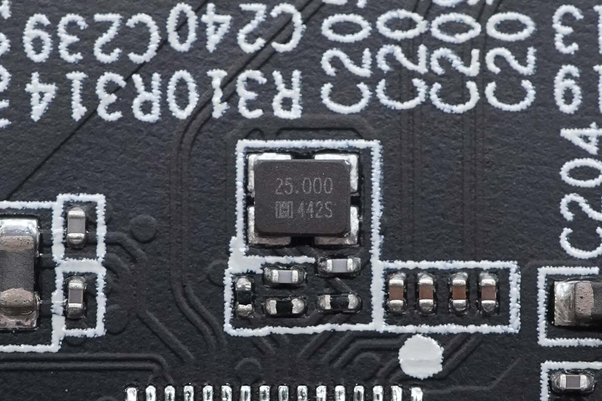
Close-up of the 25MHz clock crystal.

The memory comes from MXIC, model MX25V1006F.
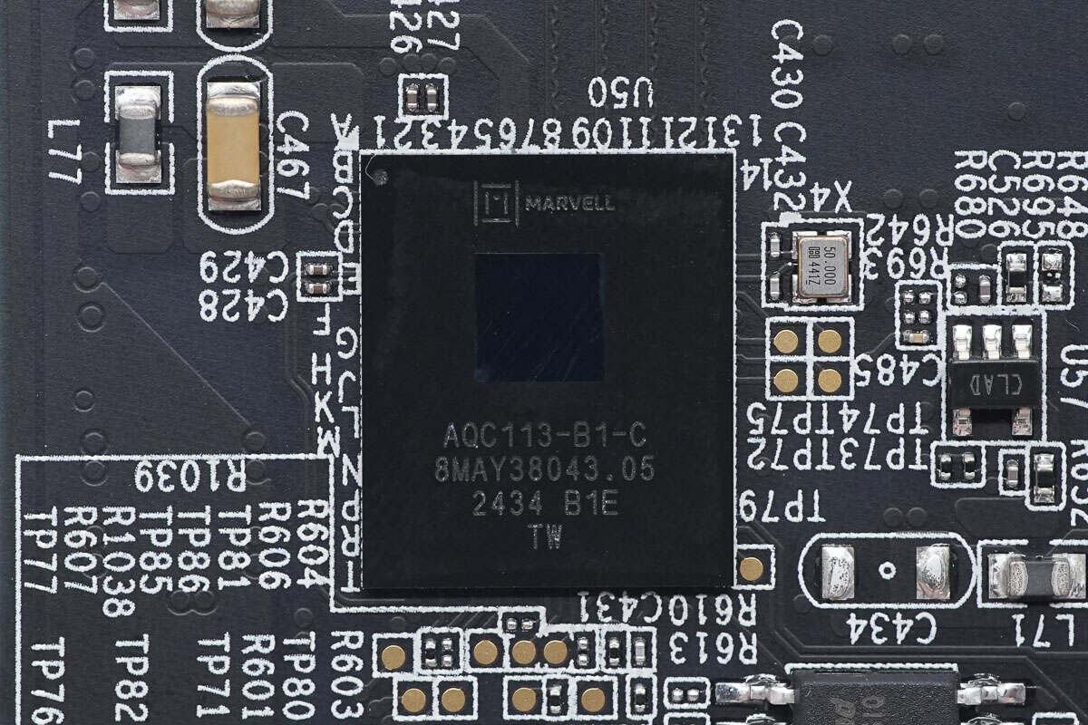
The 10 GbE network chip is from MARVELL, model AQC113. It is a high-performance, scalable Ethernet controller supporting PCIe Gen4, Gen3, and Gen2, with speeds of 10G/5G/2.5G/1G/100M/10M, and comes in an FCBGA 224 package.
The memory chip is from Winbond, model W25Q32JVSSIQ. It offers 4 MB capacity, supports a 2.7–3.6 V operating voltage range, and comes in an SOIC8 package.
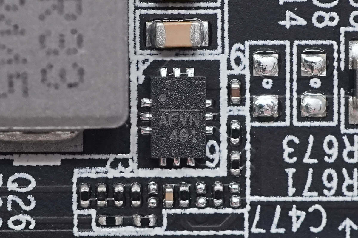
The synchronous buck converter is from MPS, marked AFV, model MP2145. It supports a 2.8–5.5 V input range, delivers 6 A output current, integrates MOSFETs, and comes in a QFN-12 package.
Close-up of the 0.33μH alloy inductor.
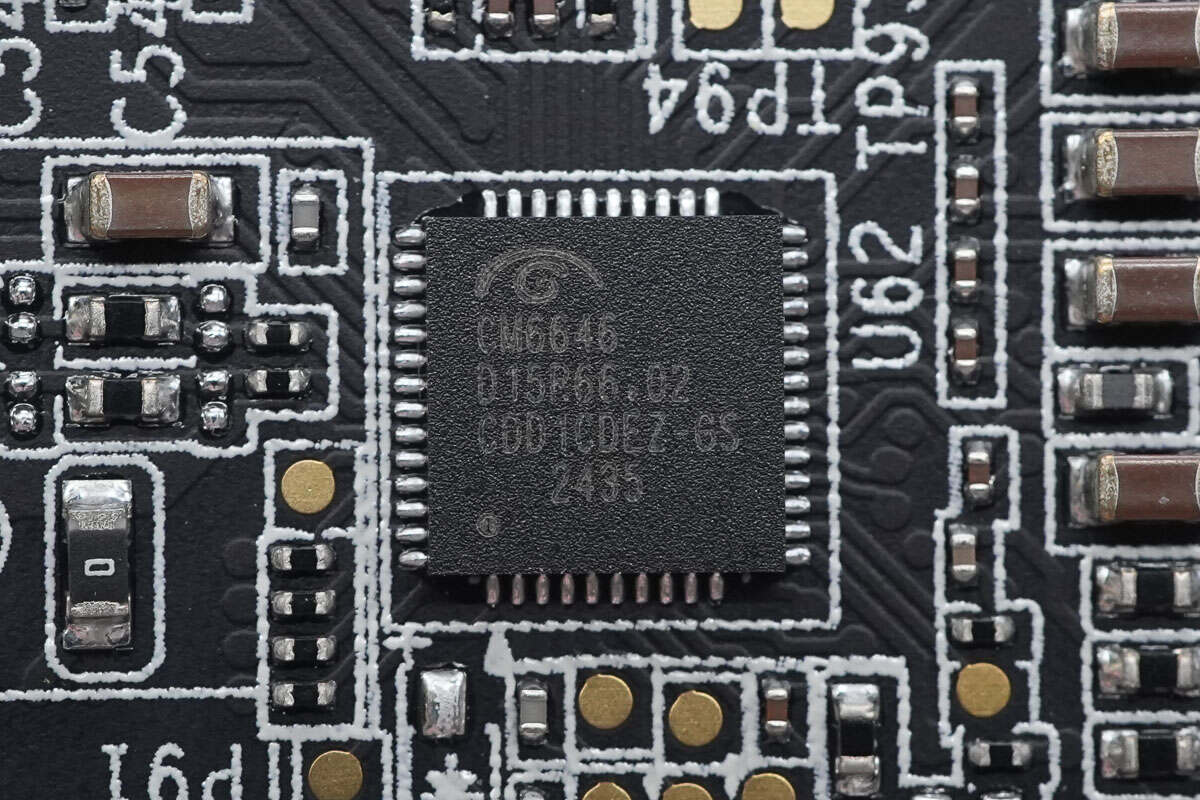
The audio chip is from Cmedia, model CM6646.
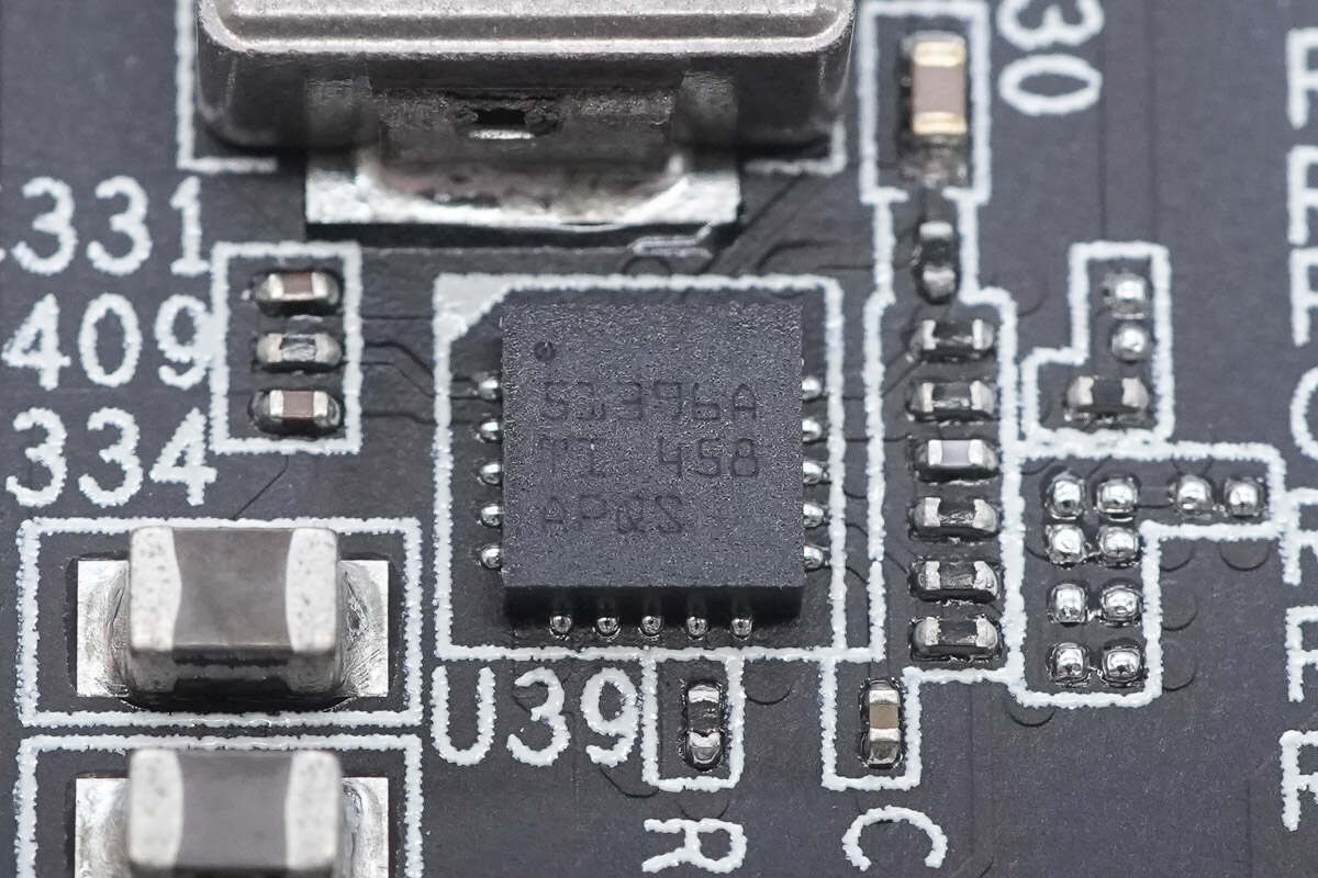
The synchronous buck converter is from Texas Instruments, model TPS51396A. It supports a 4.5–24 V input range, delivers 8 A output current, integrates MOSFETs, features fast transient response, supports 600 kHz, 800 kHz, and 1 MHz switching frequencies, and comes in a VQFN20 package.
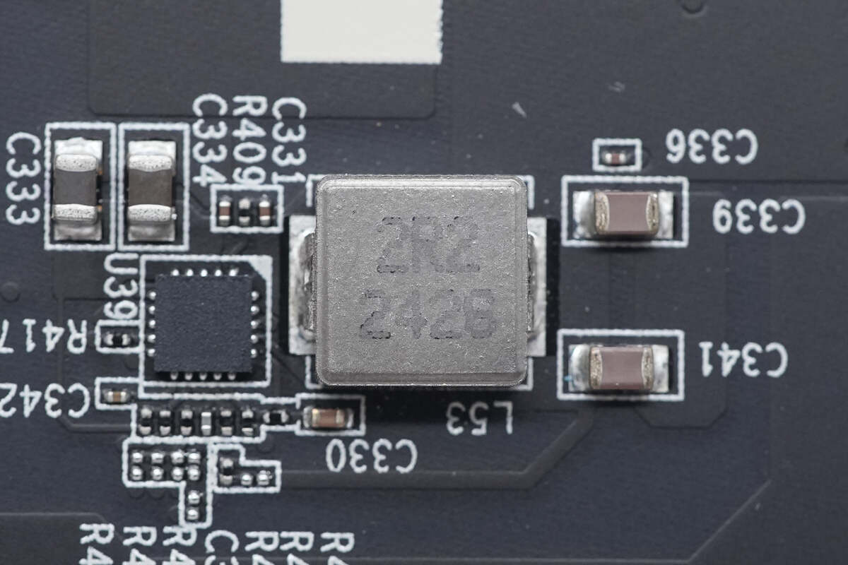
Close-up of the 2.2μH step-down inductor.
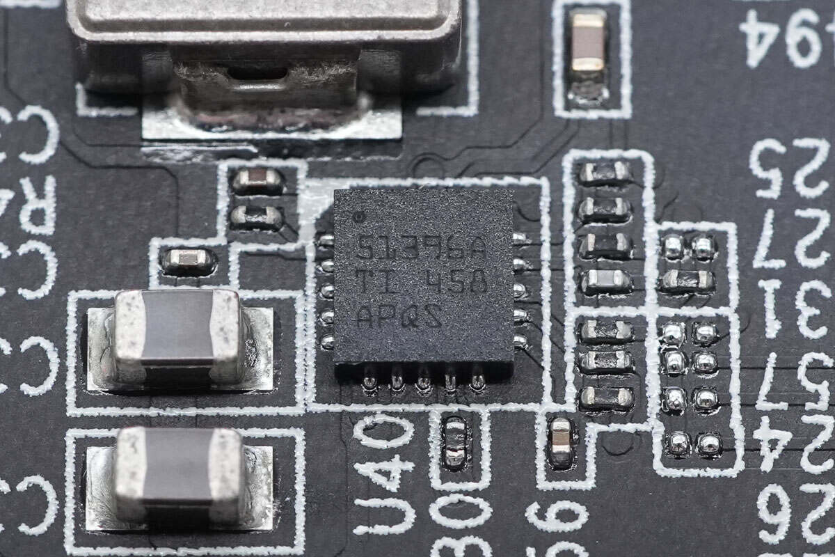
The synchronous buck chip uses Texas Instruments TPS51396A.
Close-up of the 2.2μH step-down inductor.
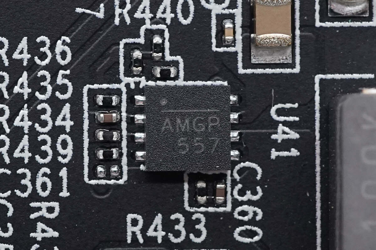
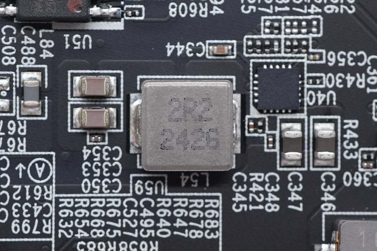
The synchronous buck converter is from MPS, marked AMG, model MP9943. It supports a 4–36 V input range, delivers 3 A output current, integrates MOSFETs, supports external clock synchronization, features output overcurrent protection and thermal shutdown, and comes in a QFN-8 package.
Close-up of the 10μH alloy inductor.
Five synchronous buck converters, model Silergy SY8088I, are used to supply different chips.
Four synchronous buck converters, model Silergy SY8089A1, are used to supply different chips.
The overcurrent protection IC is model G509.
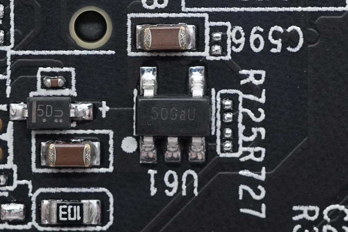
Another overcurrent protection IC uses the same model, G509.
The synchronous buck converter is from Fitipower, marked fiP, model FP6385. It supports a 2.7–6 V input range, delivers 1 A output current, allows 100% duty cycle, and comes in a SOT23 package.
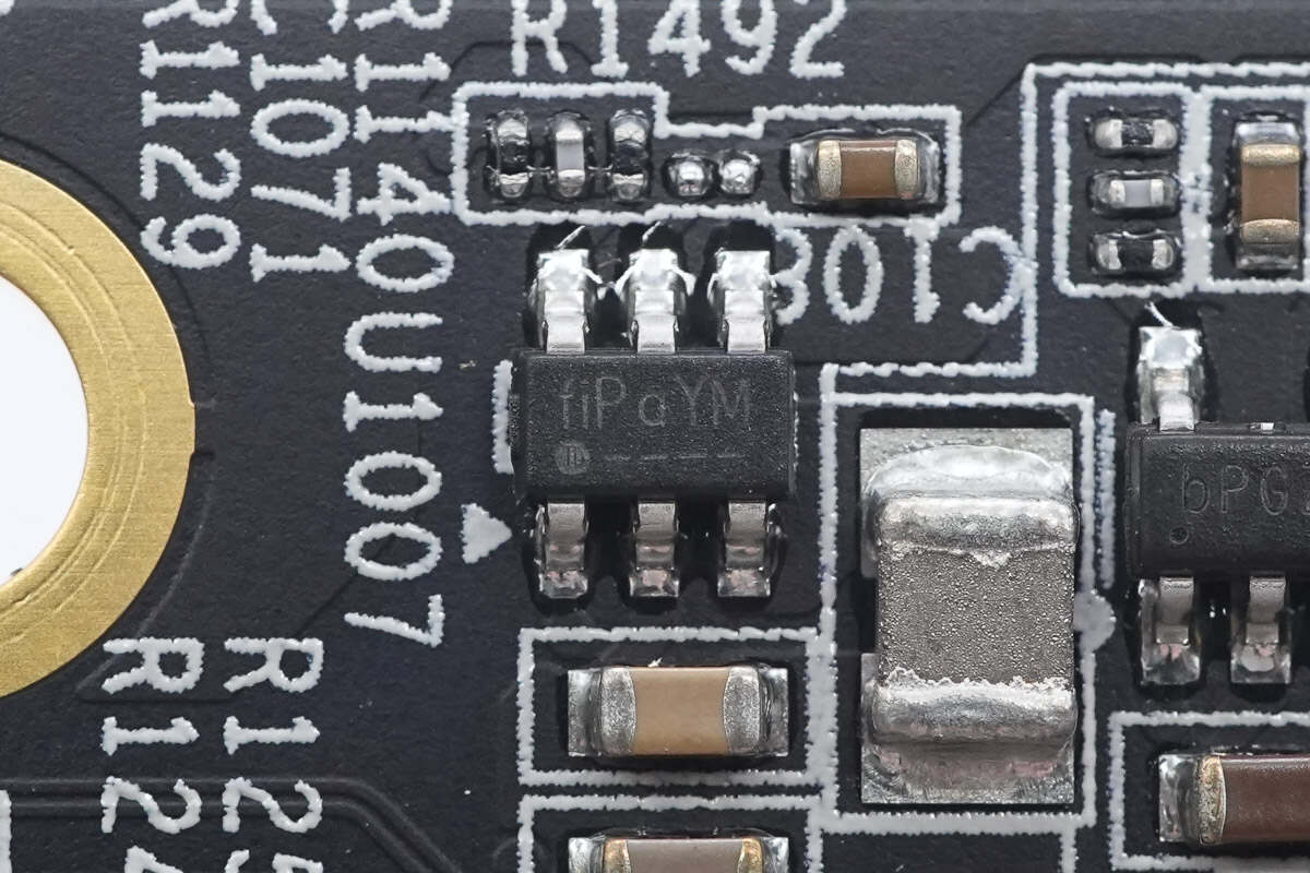
Another synchronous buck converter uses the same model, FP6385.
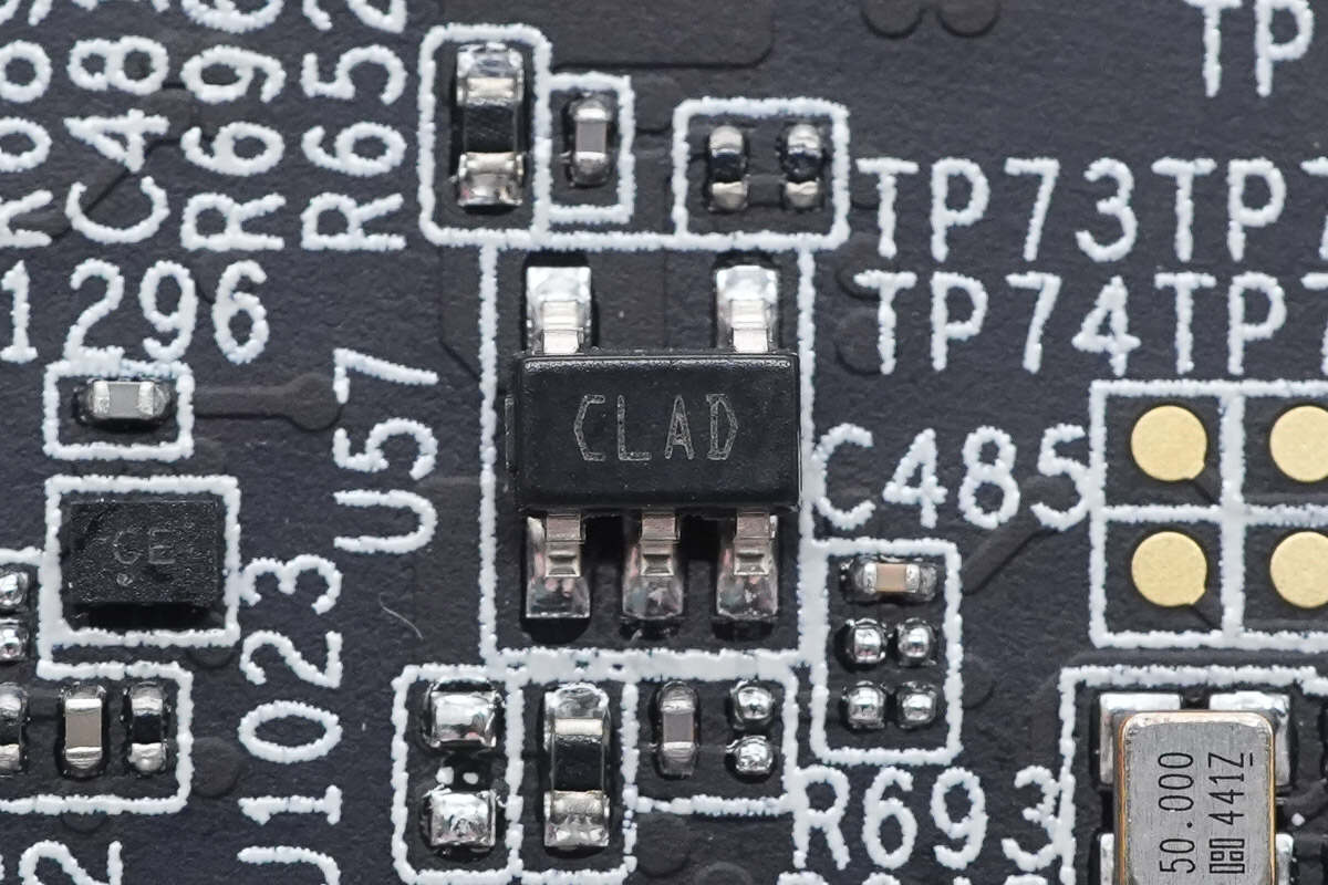
Close-up of the chip marked with CLAD.
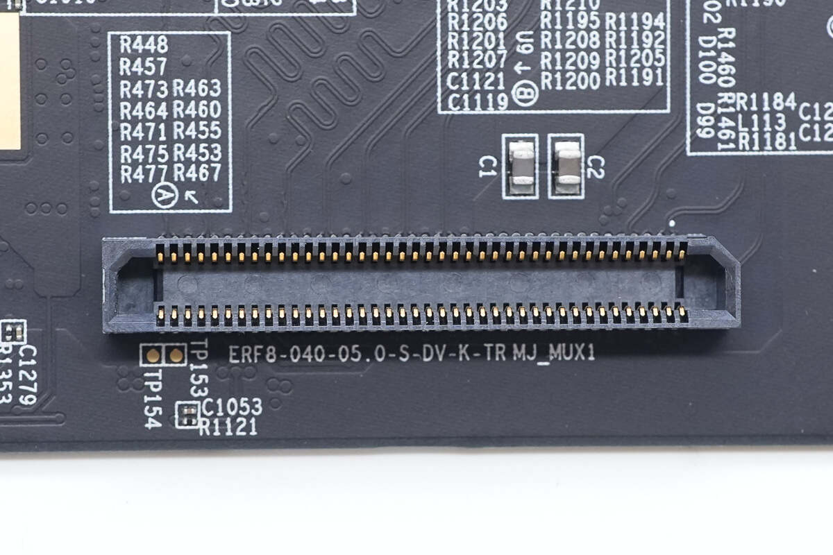
Close-up of the high-speed precision connector linking the two PCBs.
The PCBA module is equipped with a rubber pad.
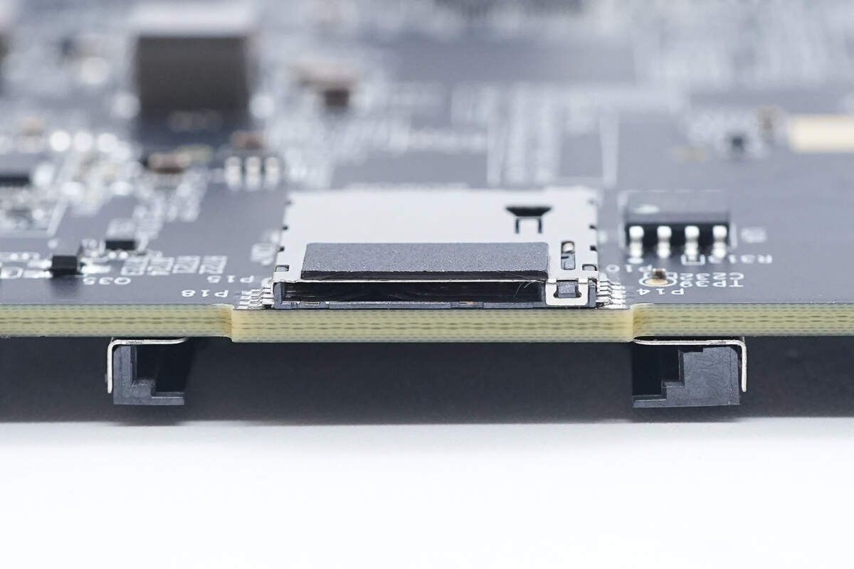
The TF card slot is mounted using surface-mount soldering.
The SD card slot is also mounted using surface-mount soldering.
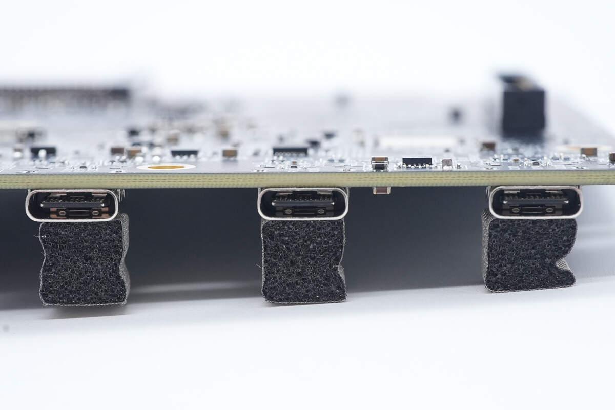
The USB-C ports are soldered through vias, with conductive fabric applied to the casing for grounding.
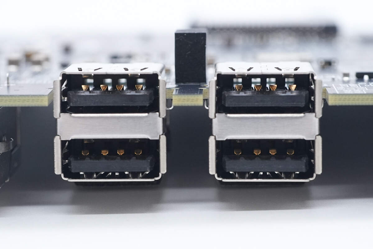
The USB-A ports are mounted using recessed soldering.
This USB-A socket is also secured using recessed soldering.
The Ethernet port is secured using through-hole soldering.
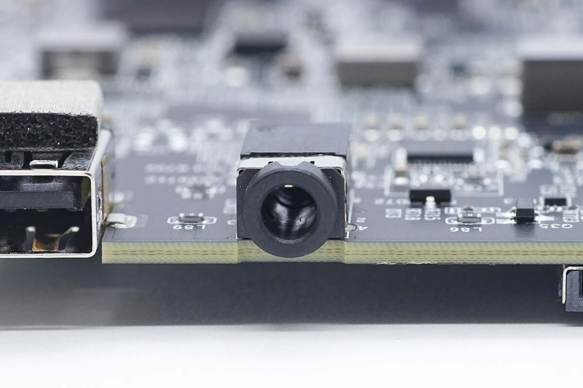
The 3.5 mm audio jack is secured using via-through soldering.
Well, those are all components of the CalDigit TS5 Plus Thunderbolt 5 Dock.
Summary of ChargerLAB
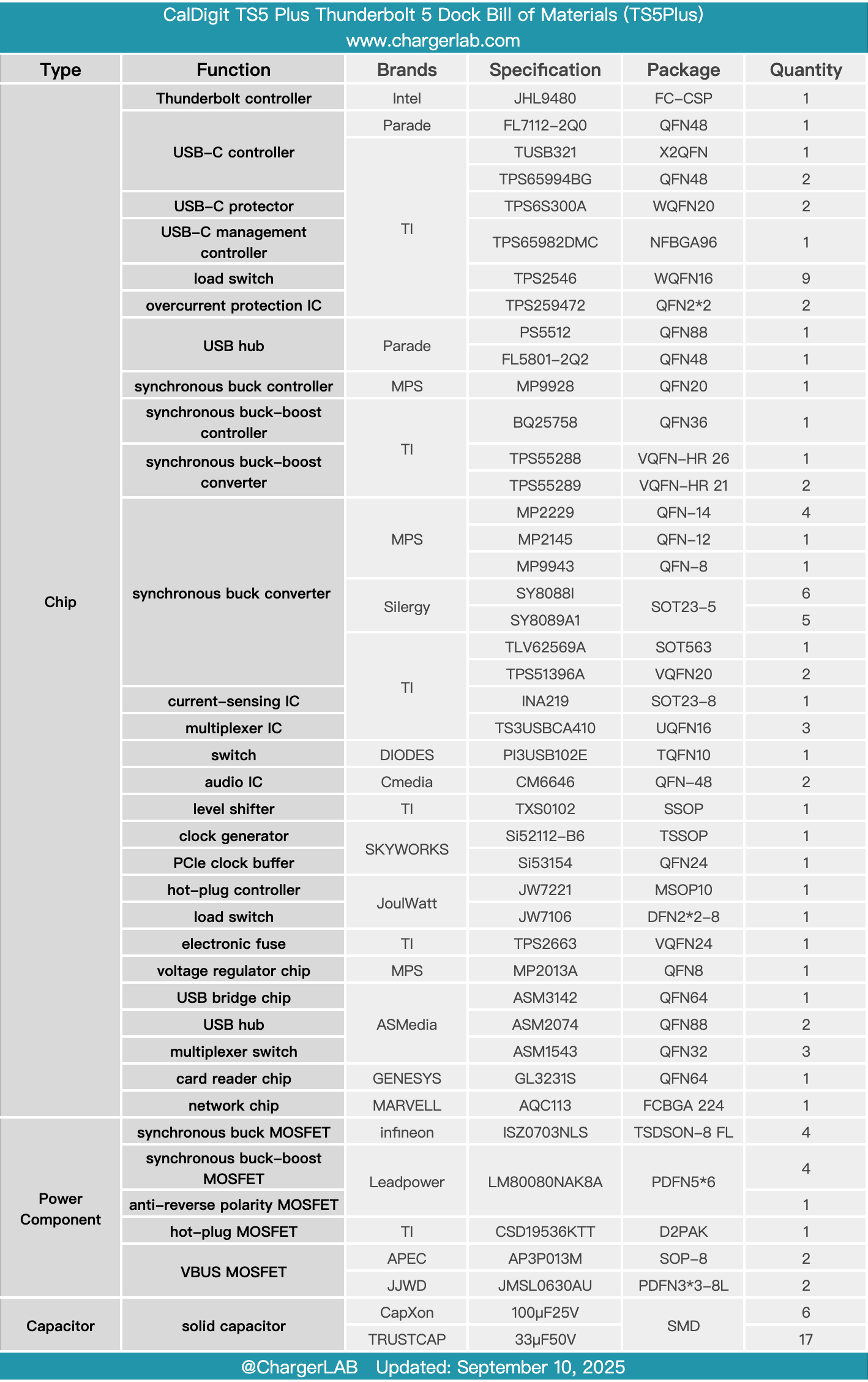
Here is the component list of the CalDigit TS5 Plus Thunderbolt 5 Dock for your convenience.
It features an aluminum alloy casing. The front panel includes USB-C and USB-A ports, as well as TF and SD card slots. The rear panel has a Thunderbolt 5 port, a 10 GbE network port, and a DP 2.1 port. The Thunderbolt 5 upstream port supports 140 W fast charging, while the Thunderbolt 5 downstream port and the front-panel USB-C port both support 36 W fast charging.
After taking it apart, we found that it contains two PCBA modules: one for Thunderbolt 5 expansion and another for other interface expansion. Heat-generating chips are thermally connected to an aluminum alloy shield via thermal pads, dissipating heat through the casing. An Intel JHL9480 Thunderbolt 5 controller manages the interface expansion, ASMedia controllers handle the USB interface expansion, and a MARVELL AQC113 chip supports the 10 GbE network port expansion.
The USB-C fast-charging port uses a Texas Instruments BQ25758 for synchronous buck-boost control, paired with a Leadpower LM80080NAK8A for voltage conversion, and filtered with TRUSTCAP capacitors to ensure efficient, stable, and reliable output, meeting the power demands of high-wattage devices. Both USB-C and USB-A ports feature dedicated overcurrent protection ICs for comprehensive protection.
Related Articles:
1. Teardown of AcBel 1100W Platinum SiC Server Power Supply (FSF056)
2. Teardown of EcoFlow RAPID Pro 140W 4‑Port GaN Charger (EF-WC-140-CN)
3. Teardown of MSI 140W USB-C Power Adapter (ADP-140AB B)