Introduction
We obtained a Belkin 140W braided USB-C to dual USB-C fast charging cable. It supports up to 140W PD 3.1, enabling charging for a wide range of devices such as laptops, tablets, and smartphones, and features intelligent power distribution. Below, we take a closer look at this product.
Product Appearance
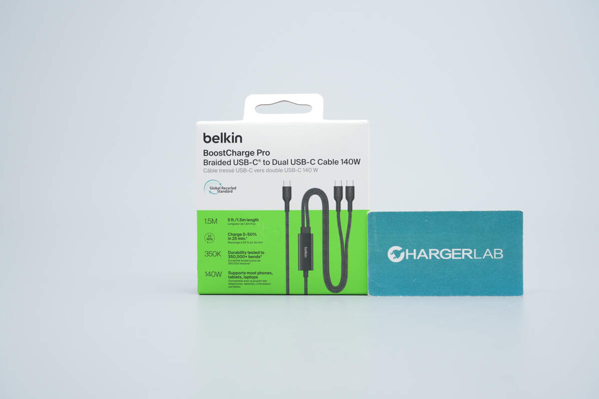
The front of the packaging displays the Belkin logo, the product name, its appearance, and key selling points.
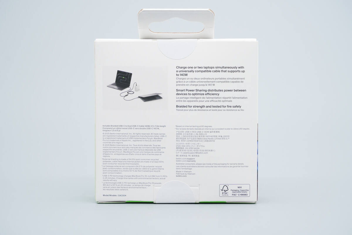
The back of the packaging shows usage scenarios for the cable along with technical specifications and other relevant information.
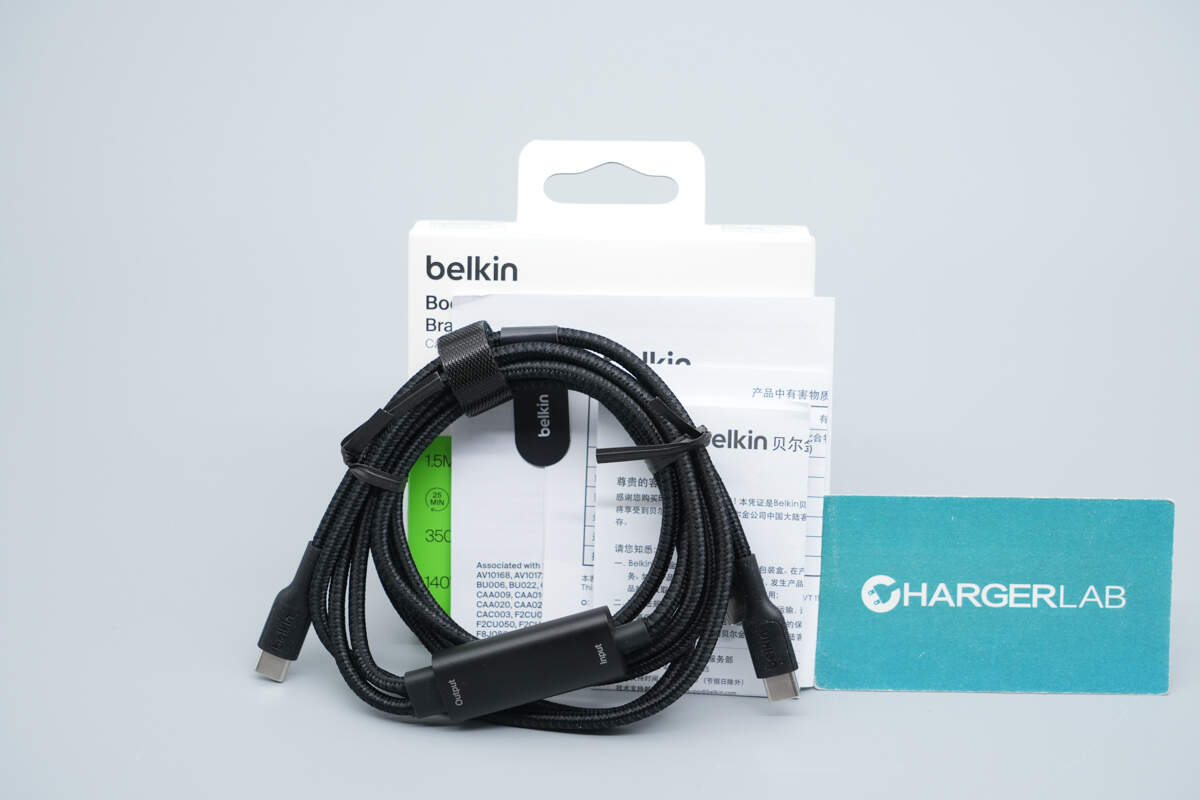
The package includes the cable, a user manual, and related documentation.
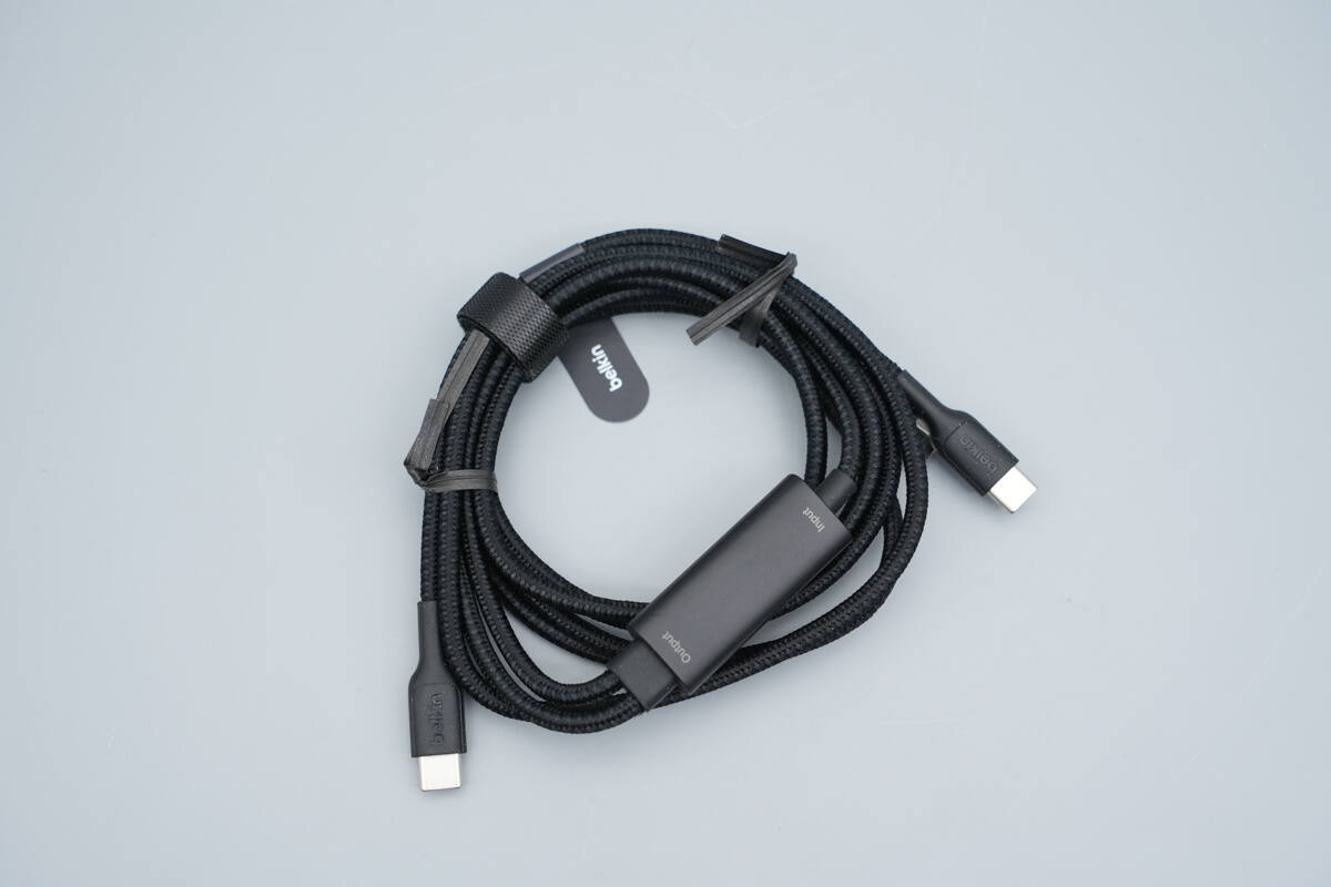
The braided cable design enhances abrasion resistance and durability, while also being more resistant to dirt and stains.
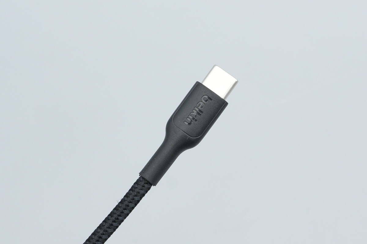
The input connector housings feature a matte finish and are engraved with the Belkin logo.
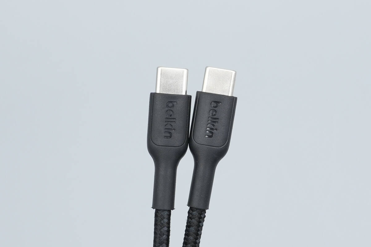
Both output connectors share the same design.
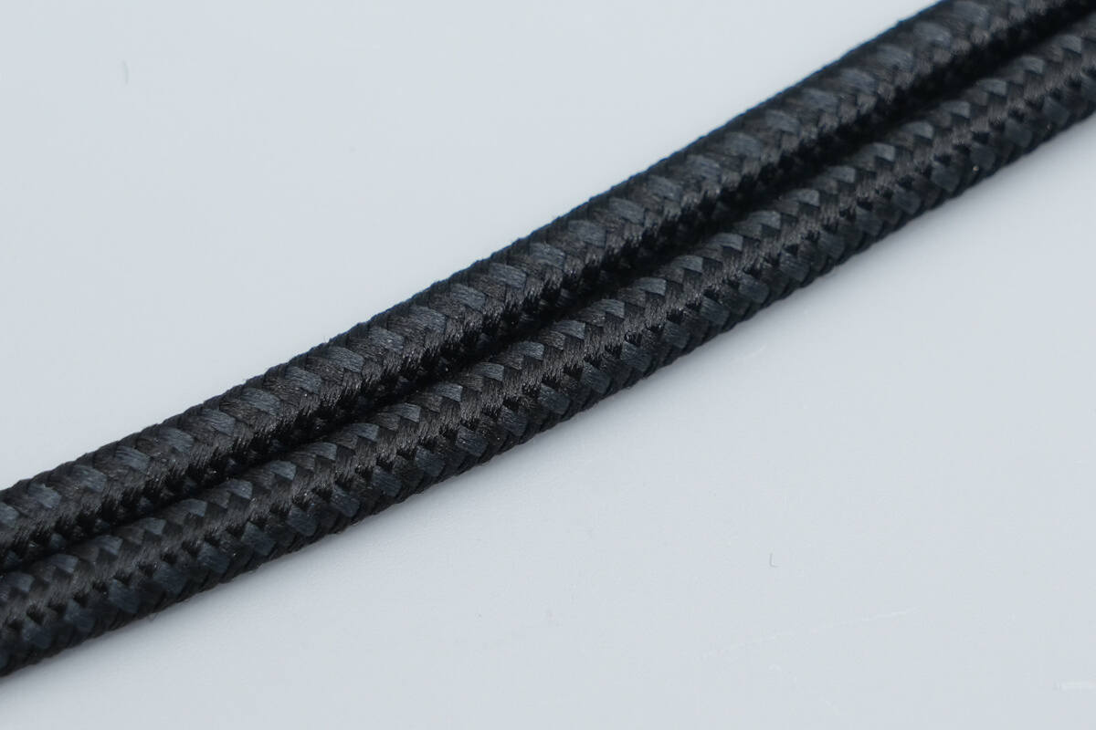
The braided outer jacket is smooth and free of burrs, reflecting a high level of manufacturing quality.
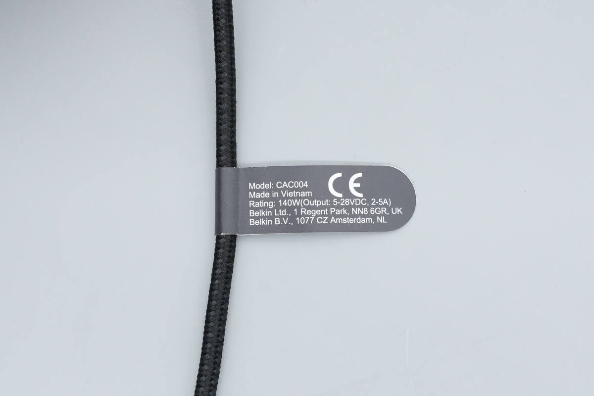
The label on the cable lists the product specifications: model CAC004, output rating of 5–28 VDC at 2–5 A, a maximum power rating of 140 W, manufactured in Vietnam, and certified to CE standards.
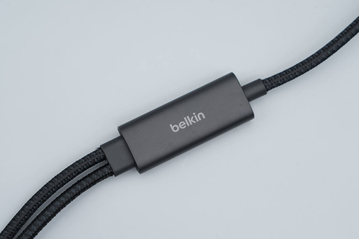
The splitter housing is made of aluminum alloy, with the Belkin logo printed at the center.
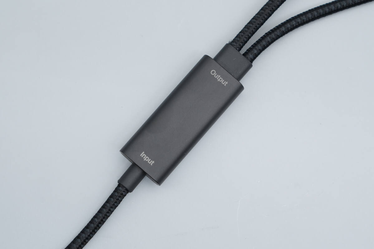
On the other side, "Input" and "Output" are printed at each end for easy identification.
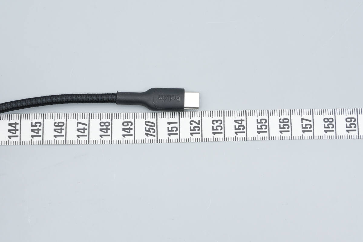
The total lighter is about 152 cm (59.84 inches).
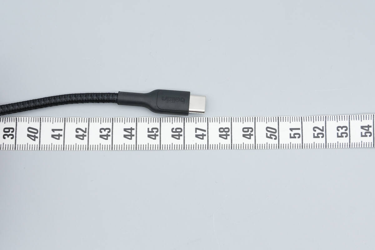
Both output cables are 47 cm (18.5 inches) in length.
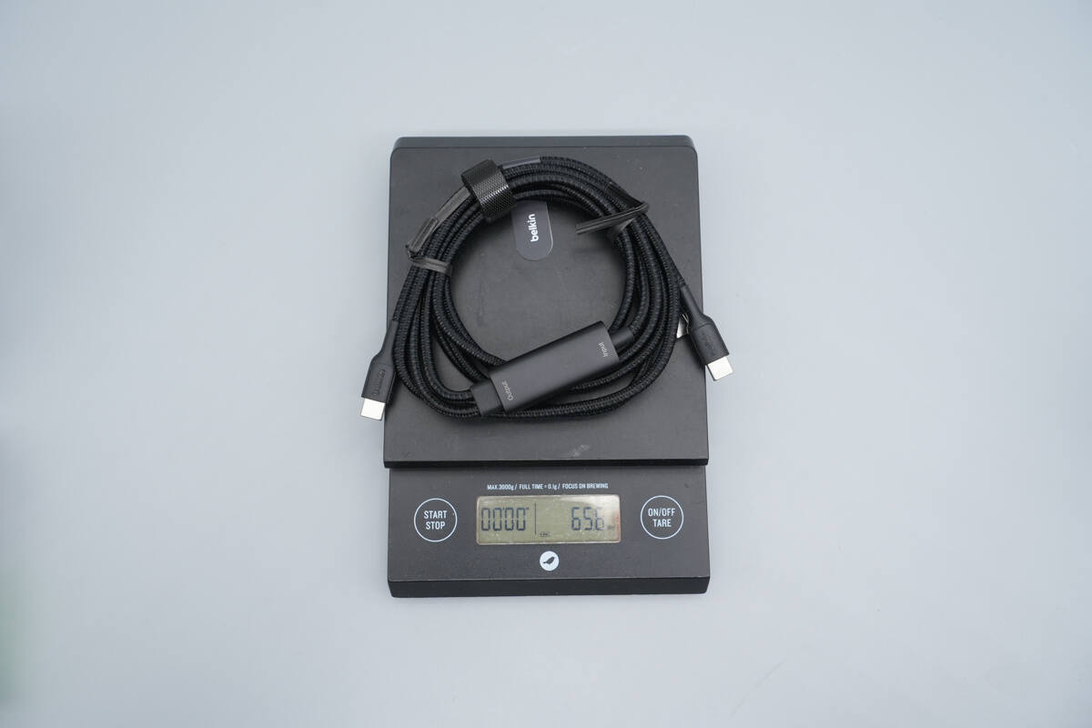
The weight is about 66 g (2.33 oz).
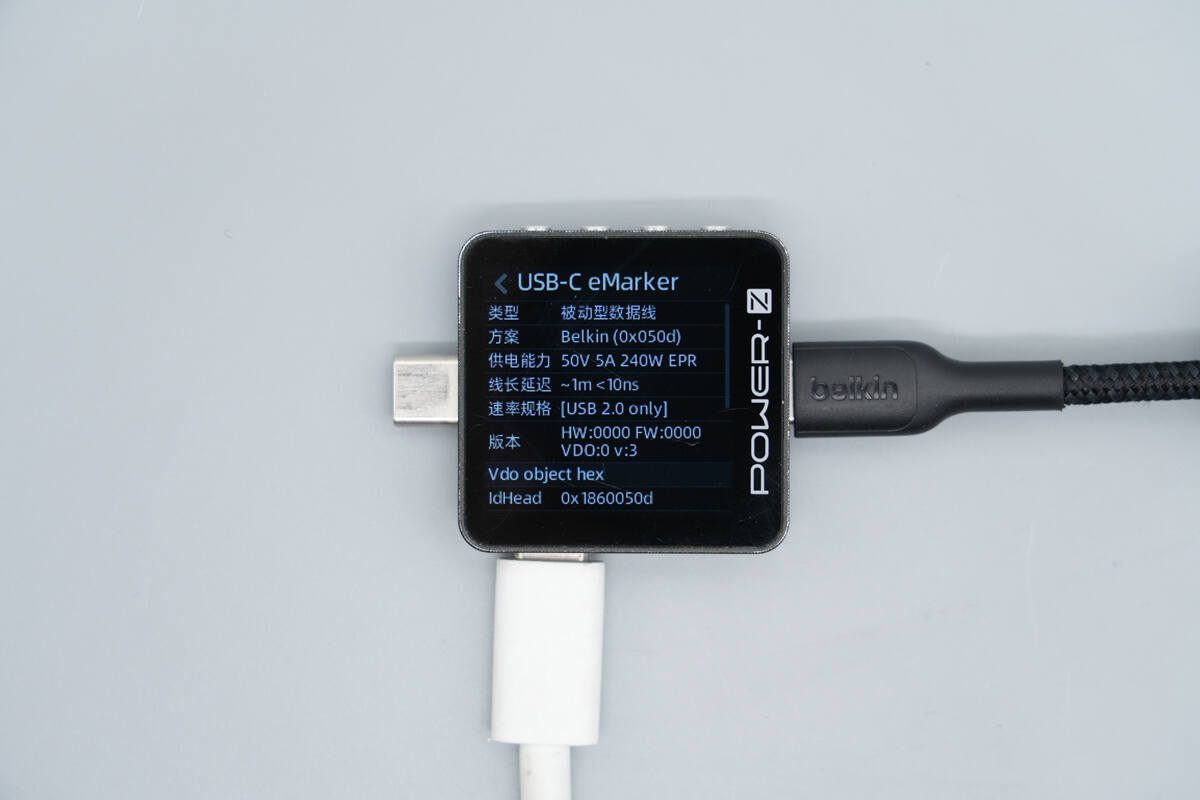
ChargerLAB POWER-ZKM003C shows it has an E-Marker chip, supporting power delivery of 50 V / 5 A and data transfer at USB 2.0 speeds.
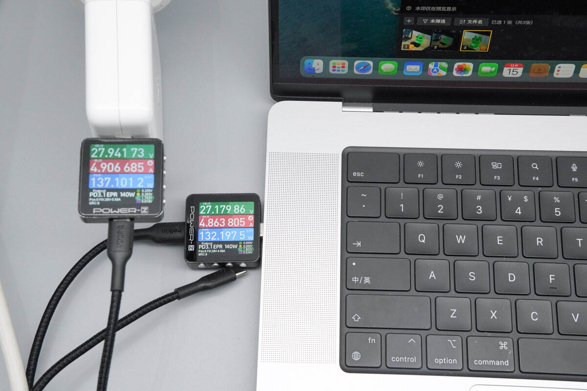
When paired with an Apple 140W charger to charge a MacBook Pro, the input power to the laptop is about 132.2 W, successfully enabling 140W PD 3.1 fast charging.
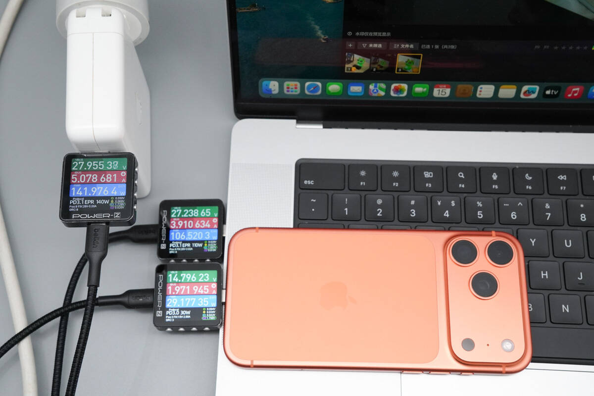
When charging a MacBook Pro and an iPhone 17 Pro Max simultaneously, the charging power is 106.52 W and 29.17 W, respectively.
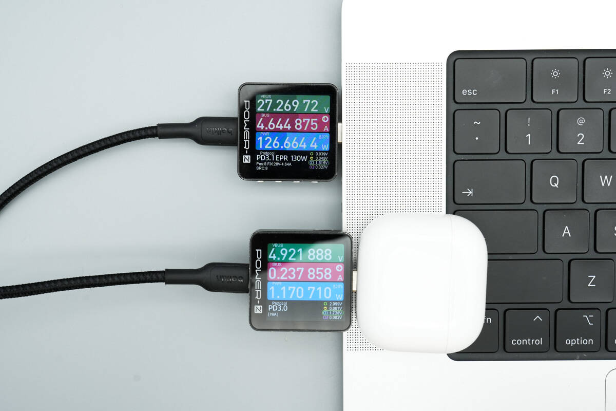
When charging an Apple MacBook Pro and AirPods Pro 4 simultaneously, the measured charging power is 126.66 W and 1.17 W, respectively.
This demonstrates that, in addition to supporting multiple fixed output combinations, the cable can intelligently distribute power based on connected devices, providing an optimal charging solution for efficient power delivery.
Teardown
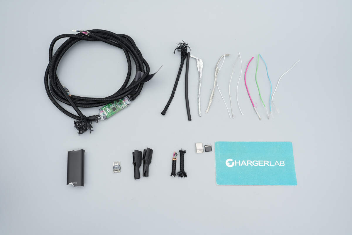
Next, let's take it apart to see its internal components and structure.
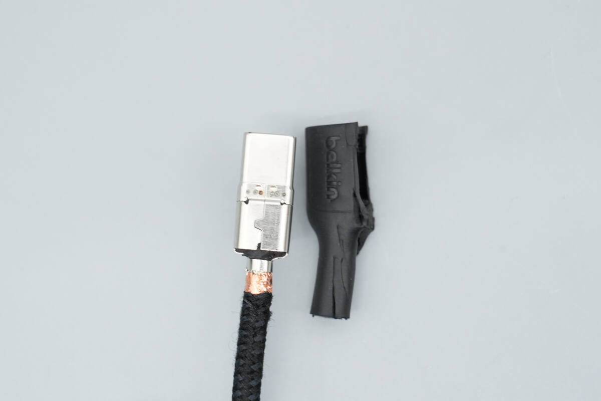
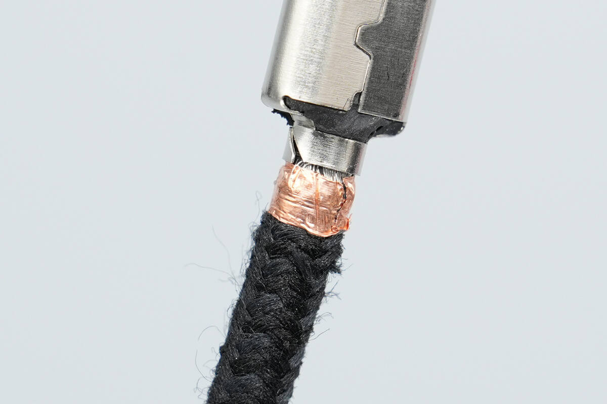
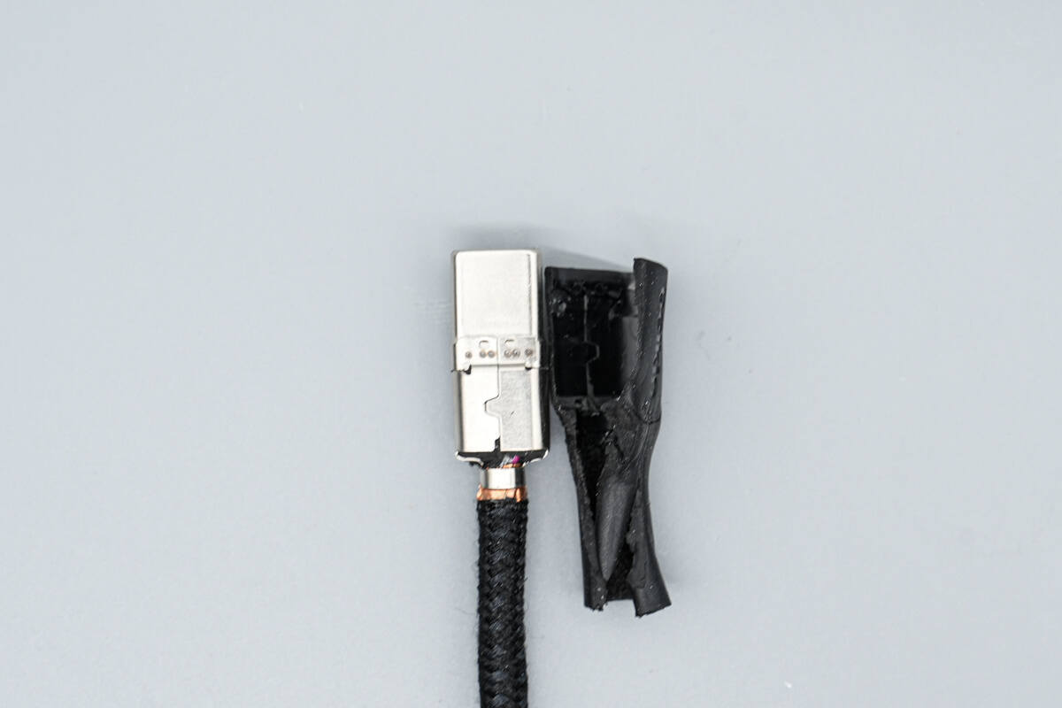
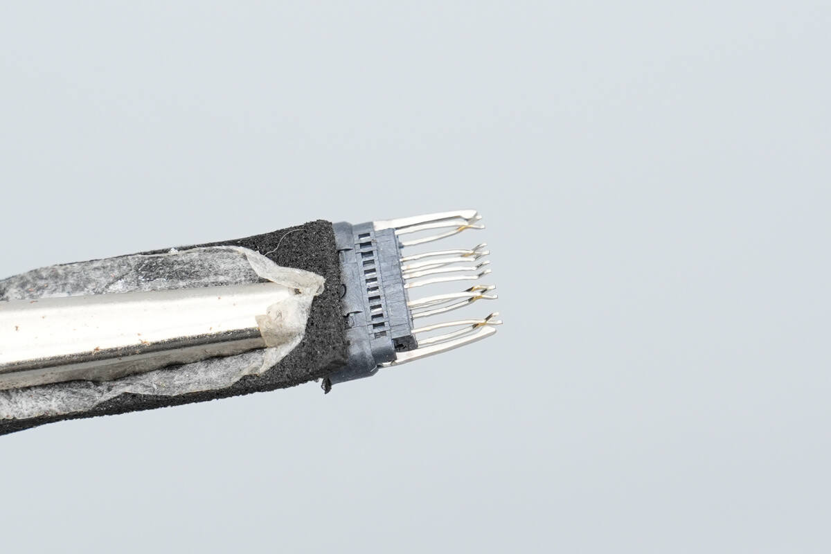
Cut open the input connector housing, revealing a metal steel sleeve inside.
The steel sleeve is spot-welded to the USB-C connector housing.
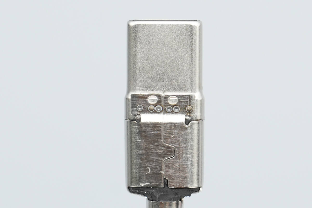
A metal clamp at the end of the steel sleeve secures the cable to prevent fraying or detachment.
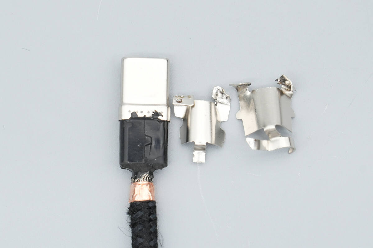
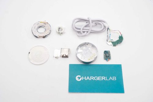
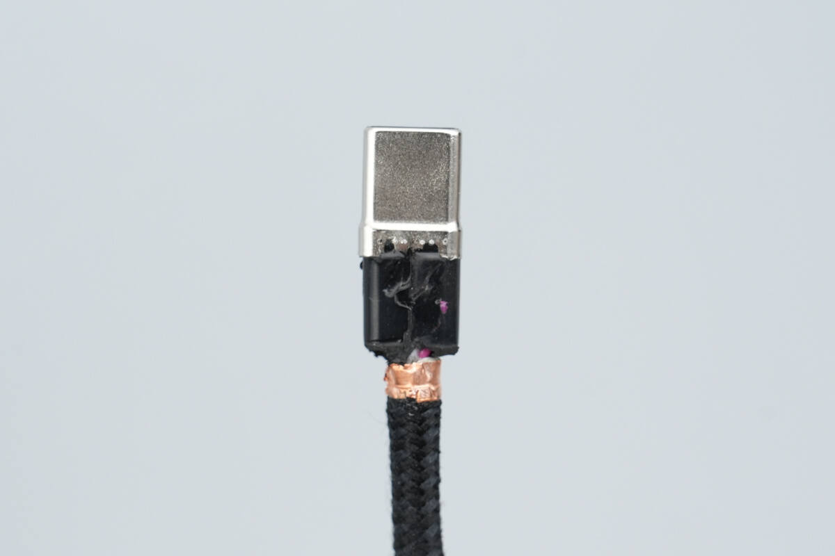
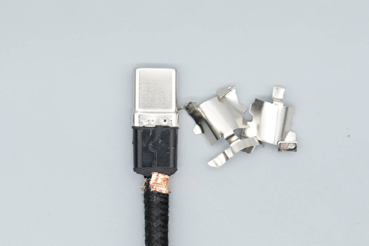
After removing the steel sleeve, the interior is filled with black hard potting compound.

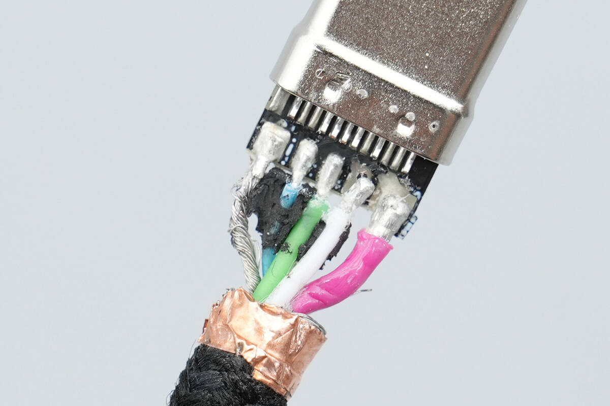
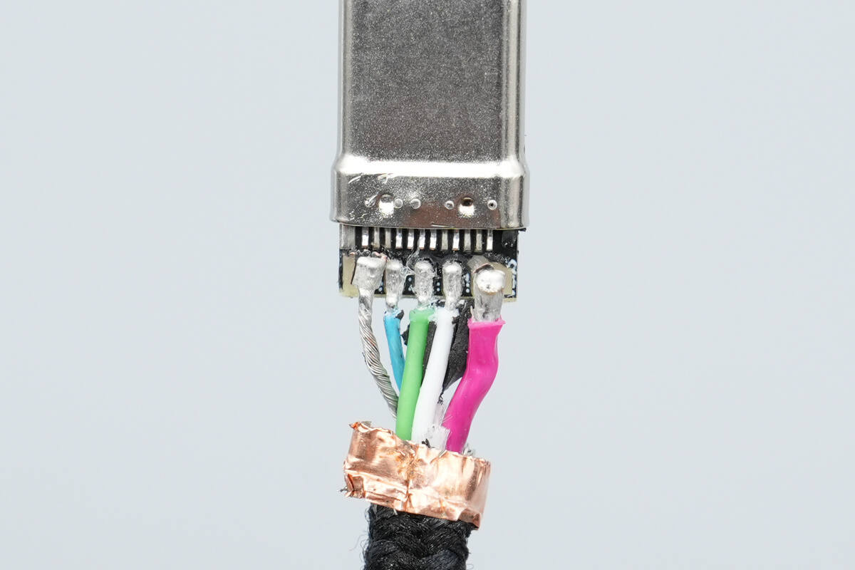
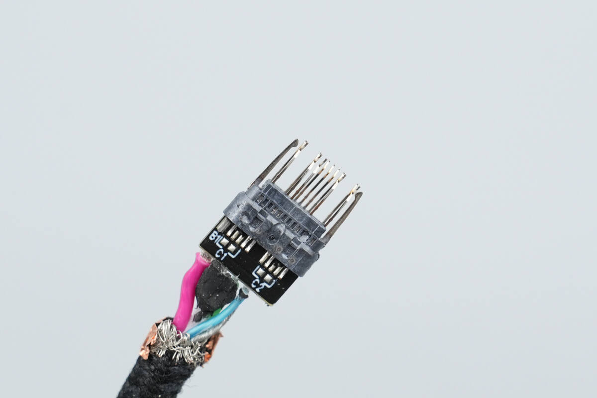
After removing the hard potting compound, a small PCB inside is revealed, with multiple wires soldered to its front side.
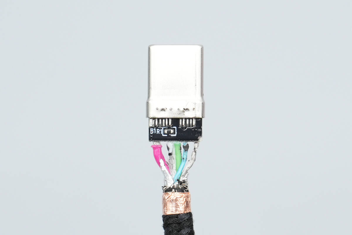
The other side of the small PCB has only a single resistor.
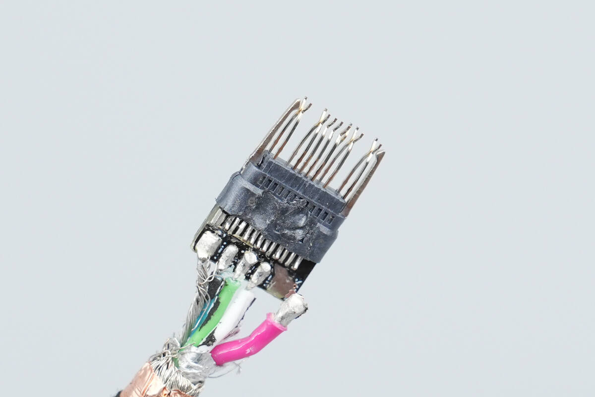
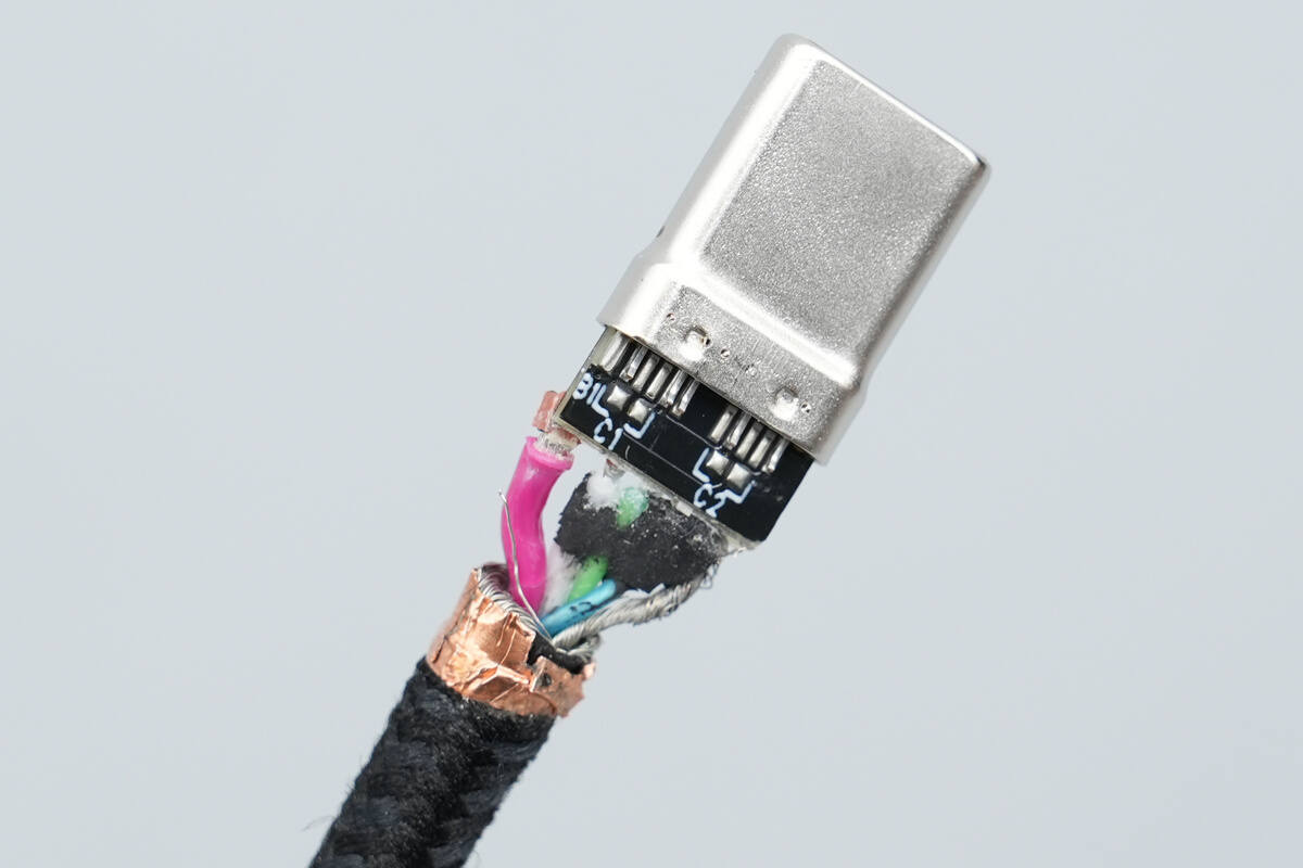
After removing the metal housing, the internal pins are found to have gold plating on their front ends.
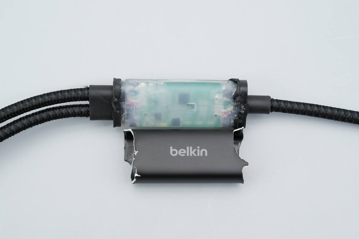
After removing the splitter’s metal housing, the interior is found to be filled with molded plastic.
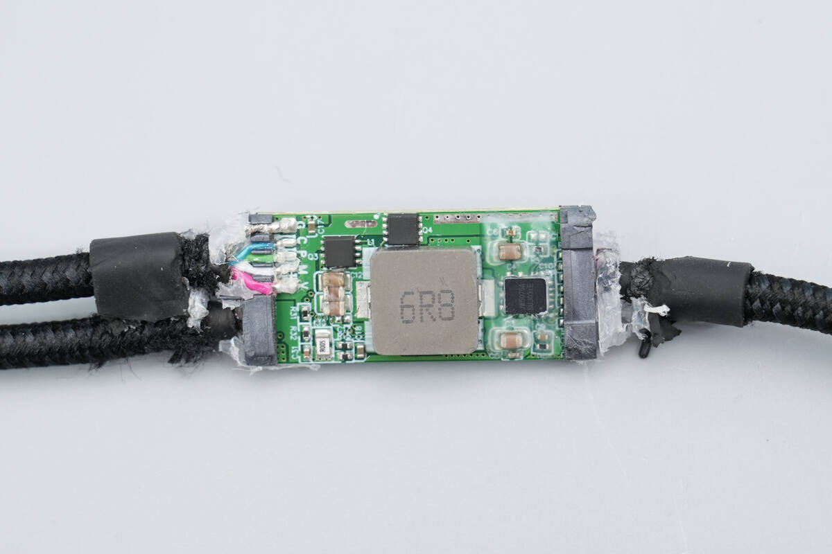
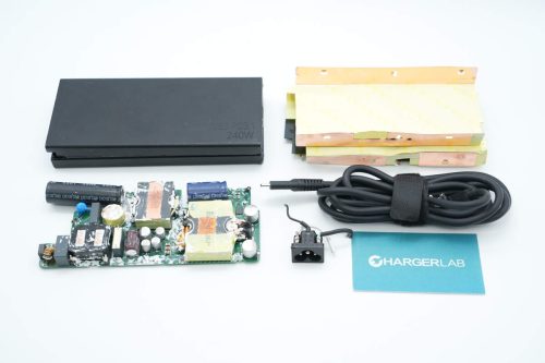
After removing the translucent plastic, the front side of the PCB reveals components such as a synchronous buck converter, a buck inductor, and VBUS MOSFETs.
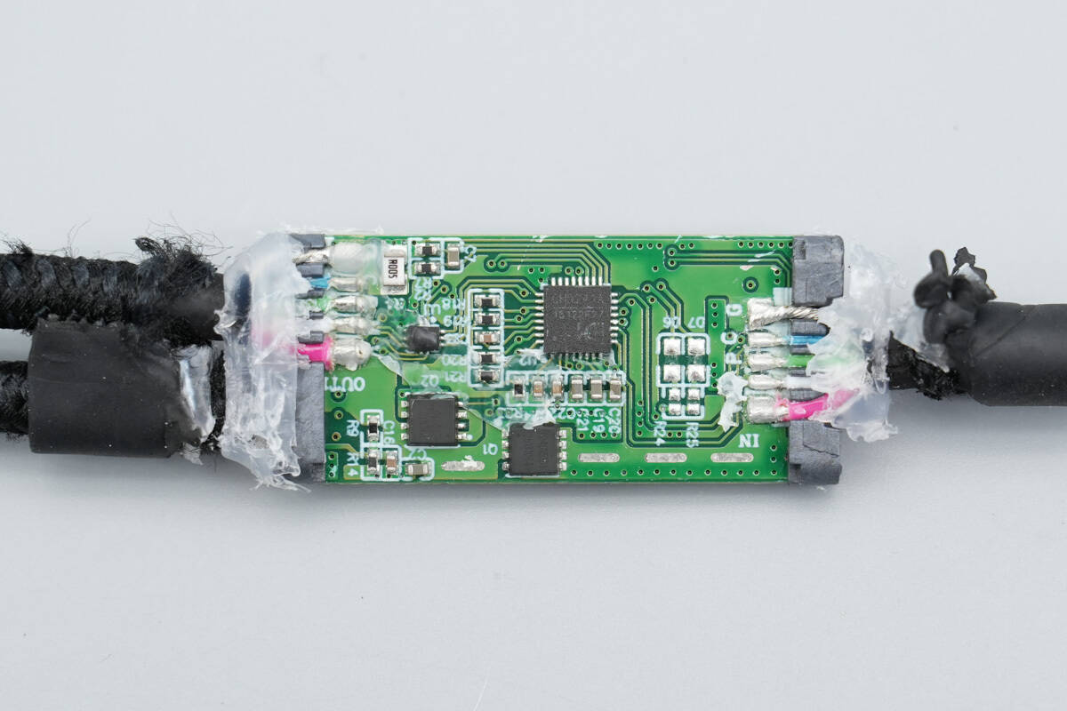
On the back side, there is a dedicated SOC for multi-output fast charging cables, VBUS MOSFETs, and an analog switch.
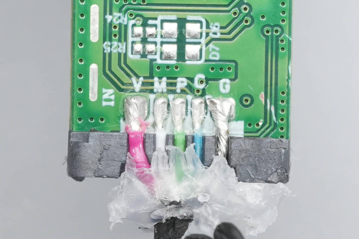
Close-up of the soldering points of the input wires.
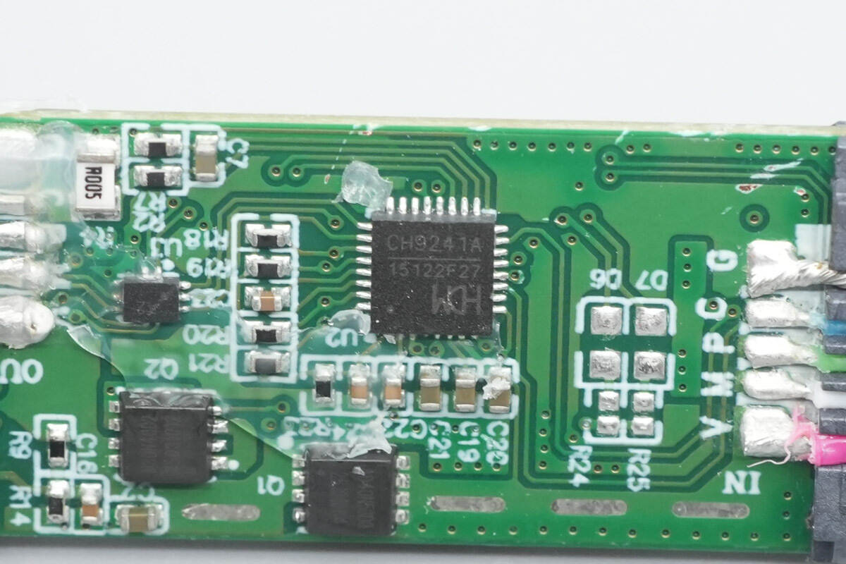
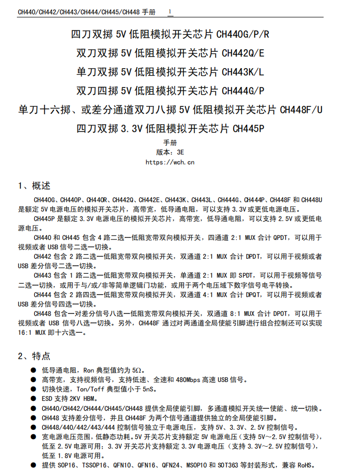
The dedicated SOC for the multi-output fast charging cable is from WCH, model CH9241A. It supports PD 3.2/3.0/2.0 protocol negotiation, power distribution, and power path switching for three ports, with a maximum PD input power of 140 W. The chip features dual output current detection, an NMOS gate boost driver, a high-voltage LDO, and E-Marker functionality. It provides over-temperature, over-voltage, current-limited output, and overcurrent protection. Additionally, it supports USB 2.0 signal selection, USB communication, and D+/D- proprietary fast charging protocols.
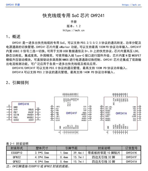
Here is the information about WCH CH9241.

The synchronous buck converter is from JOULWATT, model JW5075A. It is a 5A high-efficiency synchronous buck converter using current-mode control. It provides fast dynamic response, with a minimum on-time of only 35 ns, and can maintain stable frequency operation in high-frequency, high conversion ratio applications.
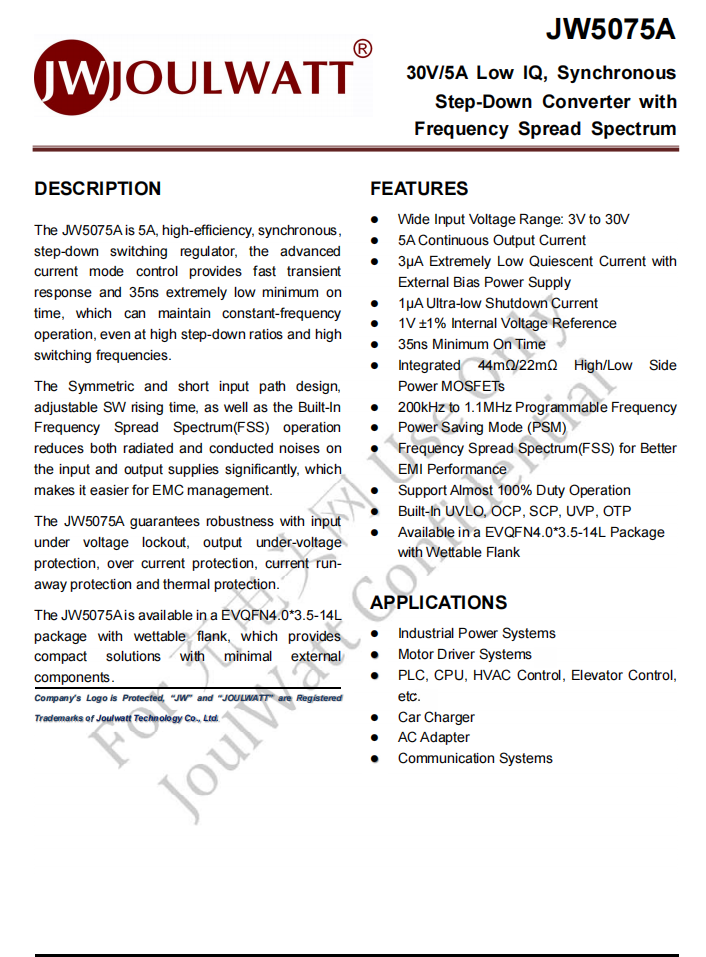
The JW5075A features a symmetrical, short-input-path design with adjustable SW rise time and built-in spread-spectrum functionality, effectively reducing conducted and radiated noise on both input and output, making EMC compliance easier.
It ensures reliability through input undervoltage protection, output undervoltage protection, overcurrent protection, short-circuit protection, and overtemperature protection. The JW5075A comes in an EVQFN 4.0 × 3.5 mm 14L package with wettable side pads, providing a compact solution with minimal external components.
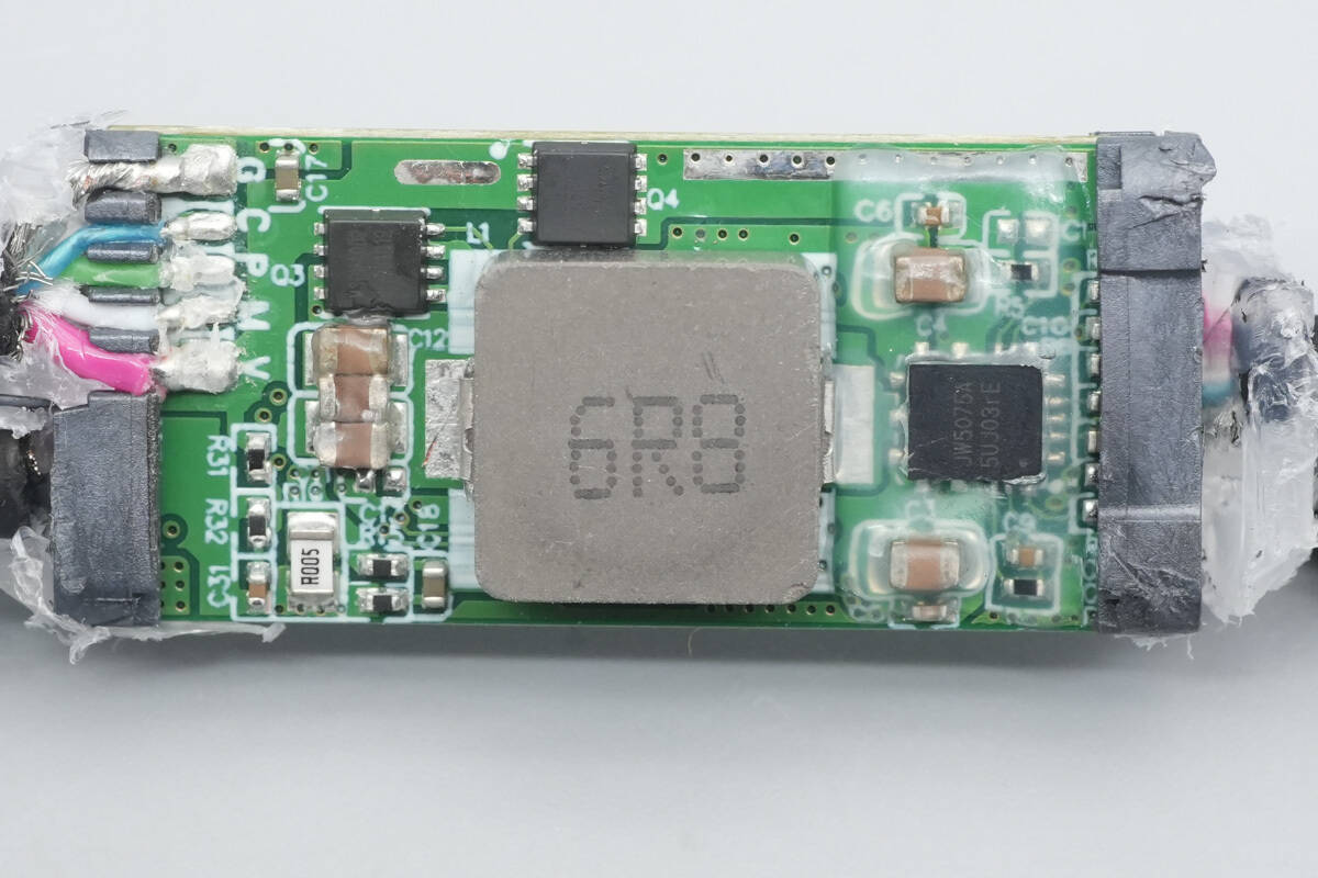
Close-up of the 6.8 μH buck inductor.

The MOSFET used for buck output switching is from Adamant, model AD40N53D3. It has a voltage rating of 40 V, an on-resistance of 4.7 mΩ, and comes in a PPAK 3 × 3 package.

The other MOSFET is marked with M30N40D2.

One of the MOSFETs in the other set is also an Adamant AD40N53D3.
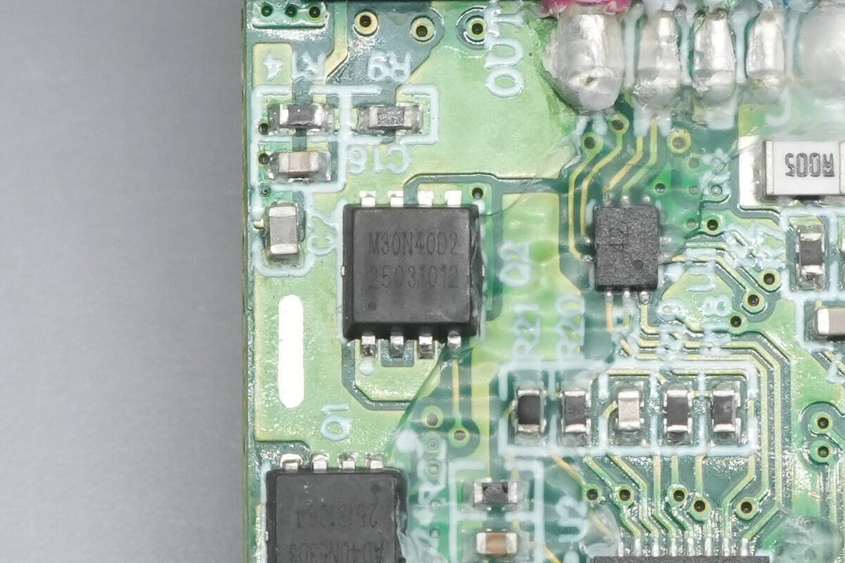
The other MOSFET is also marked with M30N40D2.
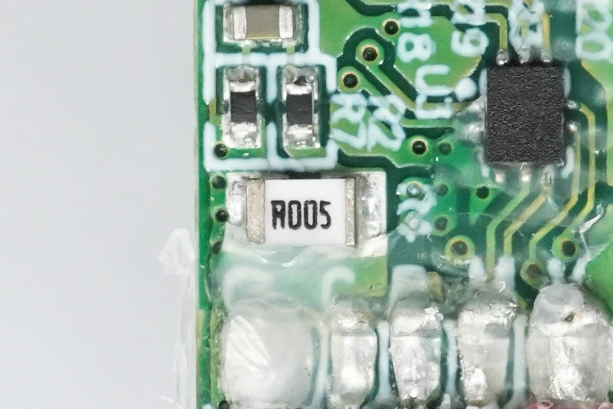
Each of the two output ports has a 5 mΩ current-sensing resistor, used to measure the charging current of connected devices for intelligent power distribution, current limiting, and overcurrent protection.
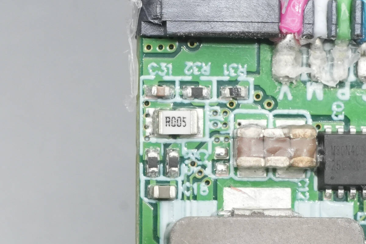
Close-up of the other current-sensing resistor.
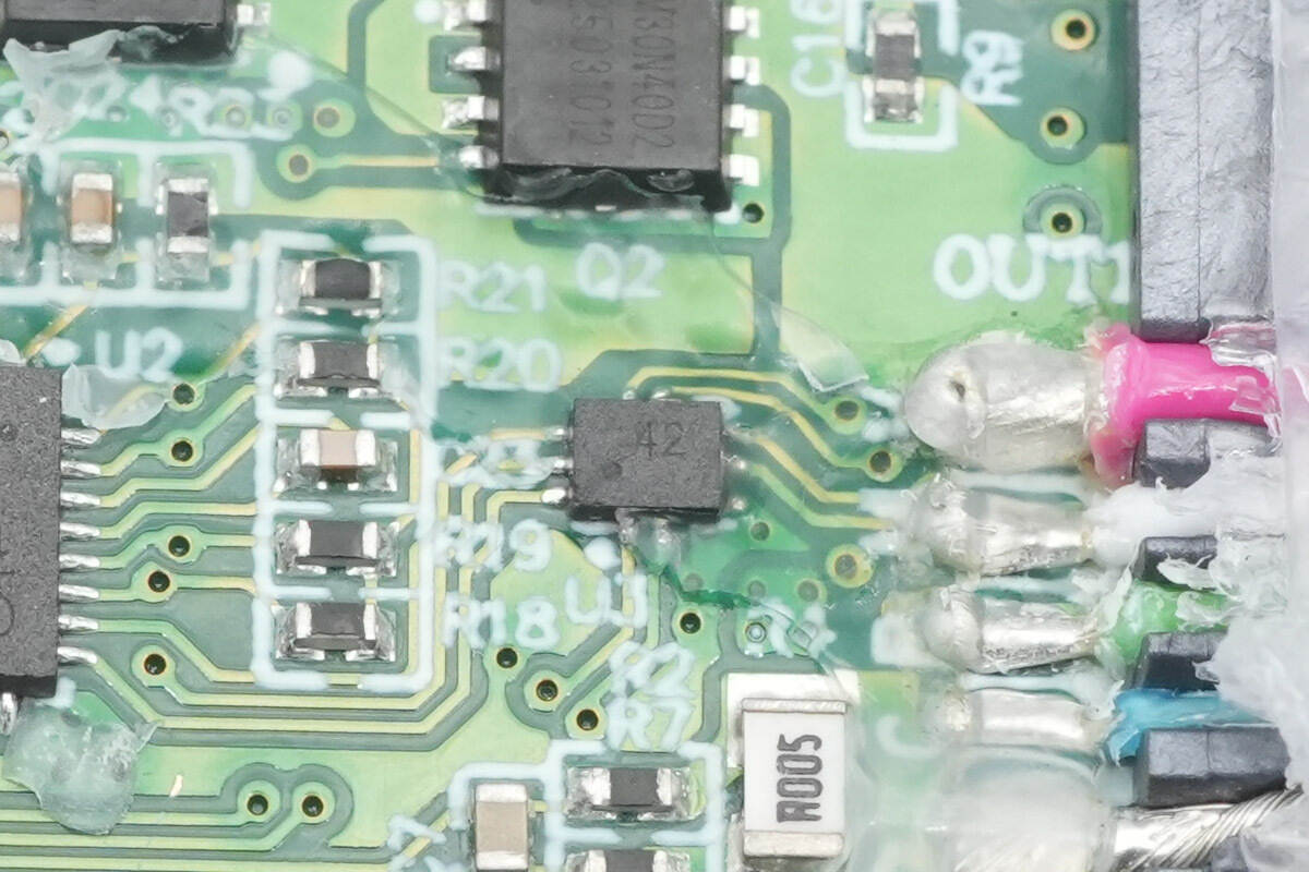
The analog switch is from WCH, marked “42” and model CH442Q. It has a rated supply voltage of 5 V, high bandwidth, and low on-resistance. It can also support 3.3 V or lower supply voltages and comes in a QFN10 package.
The CH442 contains two low-resistance, wide-band, bidirectional 2:1 analog switches, totaling a dual-channel DPDT configuration. It can be used for selecting between video or USB differential signals.
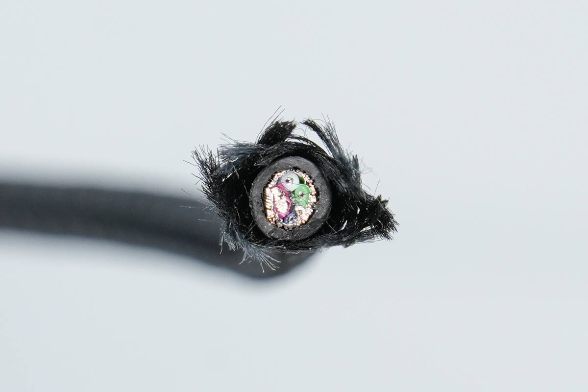
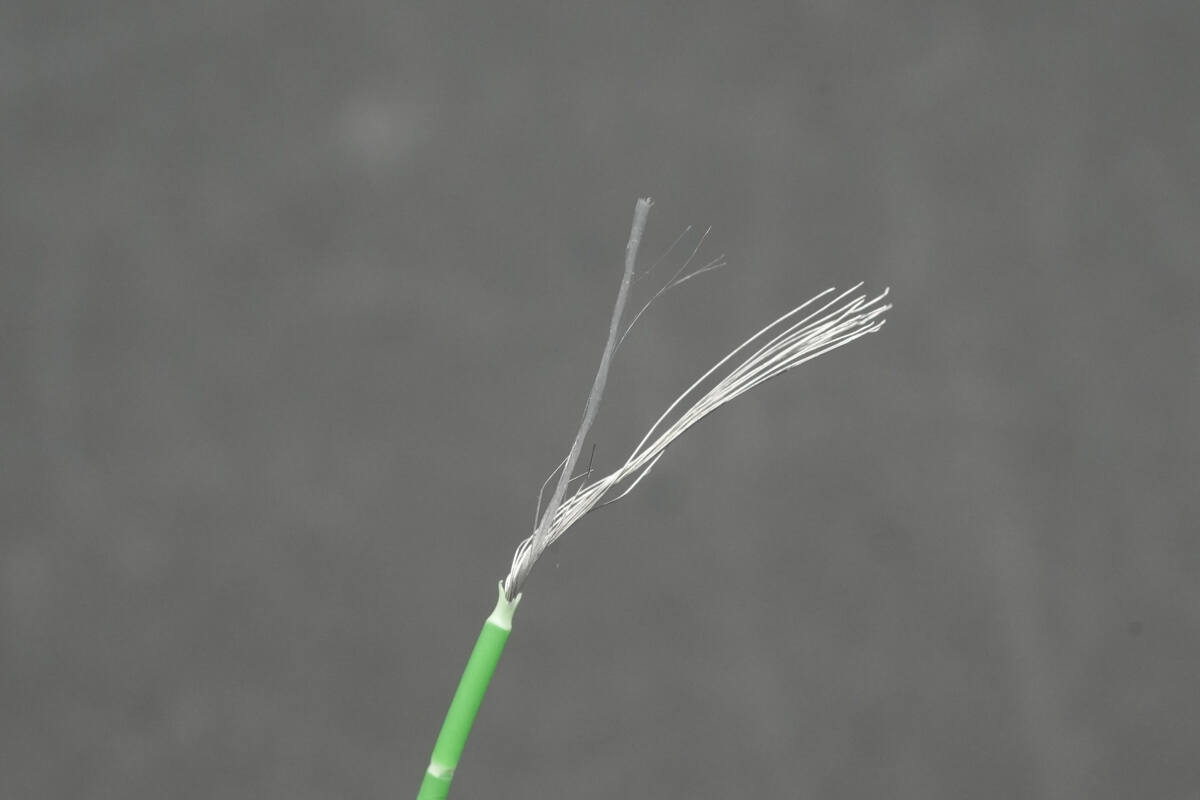
Cutting the input and output cables reveals that both contain five internal wires, with an identical design.
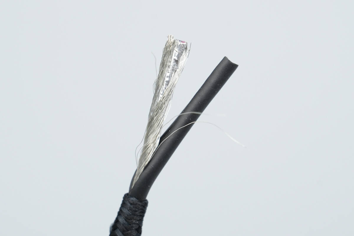
After cutting open the outer jacket, a shielding mesh and aluminum foil are found inside.
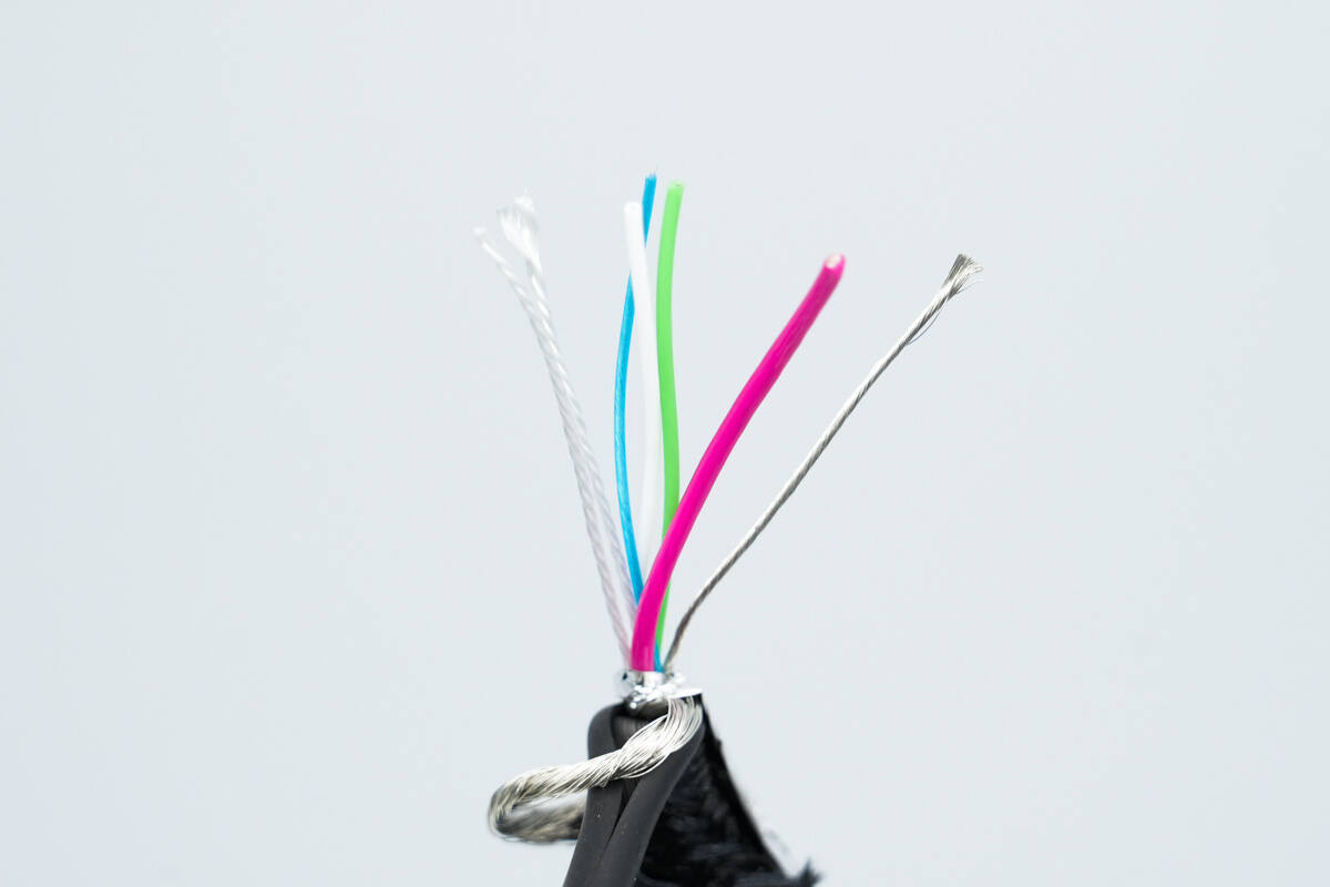
Beneath the aluminum foil shielding are a red positive power wire, a bare negative power wire, a green D+ wire, a white D– wire, a blue CC wire, and two strain-relief wires.
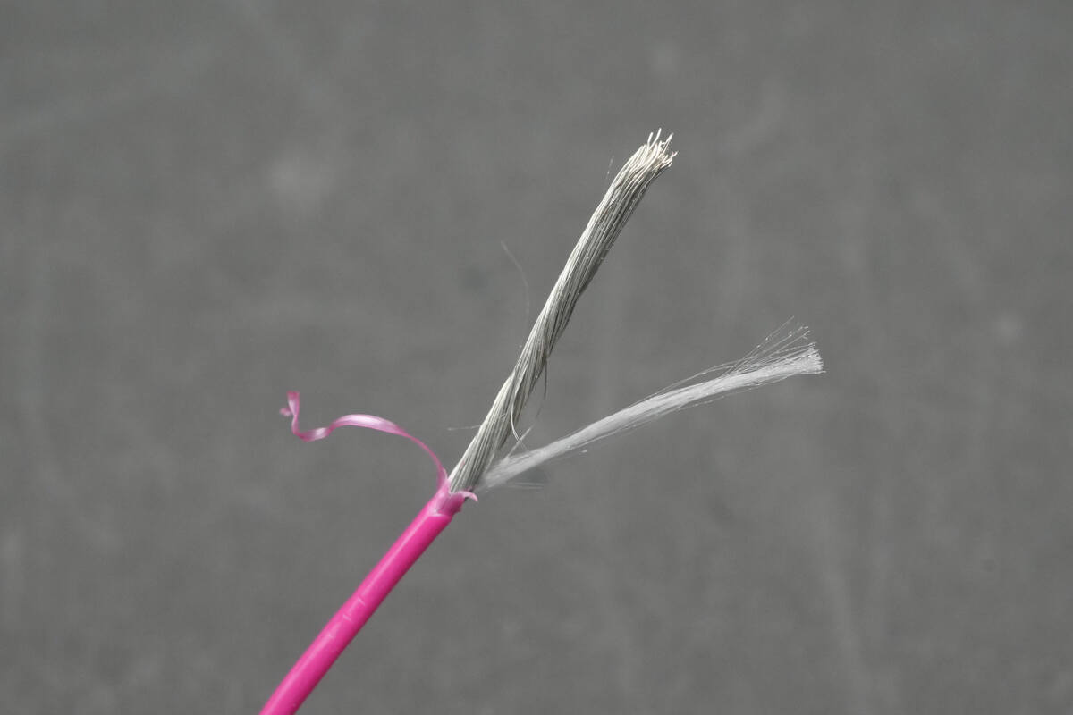
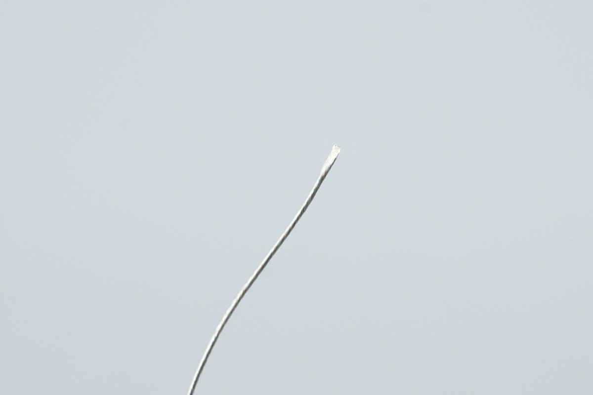
The positive power wire incorporates strain-relief fibers internally to enhance its tensile strength.
Close-up of the negative power wire.
The green D+ wire is used for USB 2.0 data transmission and also contains internal strain-relief fibers.
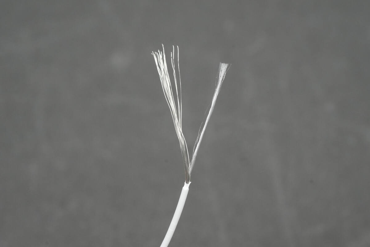
The white D– wire is used for USB 2.0 data transmission and also contains internal strain-relief fibers.

Close-up of the blue CC wire.
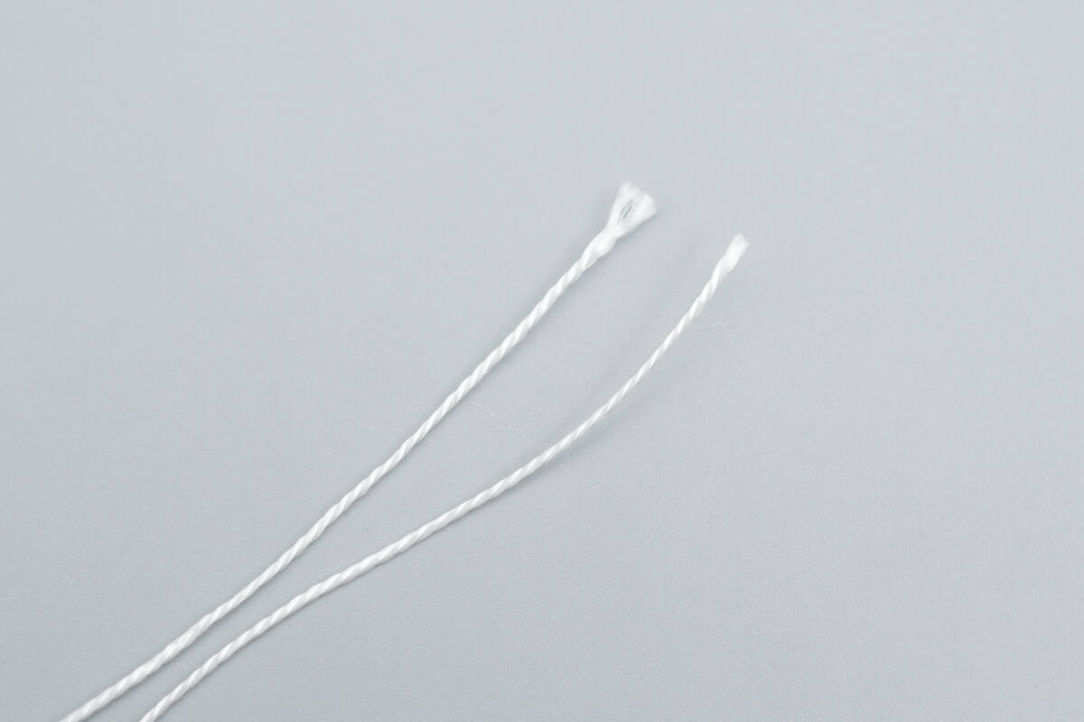
Close-up of the two strain-relief wires.
Cut open the output connector housing, revealing a metal steel sleeve inside.
The interior of the steel sleeve is filled with black hard potting compound.
The front side of the internal PCB has five wires soldered to it.
Overview of the back side of the small PCB.
Close-up of the pins.
The other output cable uses the same design.
Close-up of the five wires soldered on the PCB.

Overview of the other side.
Close-up of the pins.
Well, those are all components of the Belkin BoostCharge Pro 140W Braided USB-C to Dual USB-C Cable.
Summary of ChargerLAB
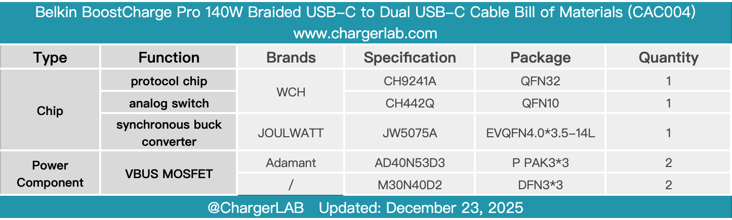
Here is the component list of the Belkin BoostCharge Pro 140W Braided USB-C to Dual USB-C Cable for your convenience.
It features a braided design and has been officially tested to withstand 350,000 bends and 20,000 plug-in cycles, demonstrating exceptional durability. Belkin also provides a 2-year warranty. The cable supports up to 140 W output and multiple power combinations, including 100 W + 40 W, 82 W + 18 W, 66 W + 33 W, and 50 W + 50 W, covering the charging needs of most users. Its data transfer speed reaches 480 Mbps, suitable for everyday office and study tasks.
After taking it apart, we found that it uses the WCH CH9241A dedicated SOC for the multi-output fast charging cable. Its high level of integration not only reduces design complexity but also optimizes system costs, enabling intelligent adaptive power distribution while allowing fast charging and data communication to run simultaneously, enhancing the user experience.
Related Articles:
1. Teardown of Baseus T-Space 3rd Generation 60W GaN Charger Dock for Tesla (BS-TS017)
2. Teardown of Anker Prime 14-in-1 Docking Station (A83B3) – Black Myth: Wukong Edition
3. Teardown of Laifen i2 Sweeping & Vibrating Electric Toothbrush (LFTB02-PT)