Introduction
Today, we will dissect the Belkin 112W GaN fast charger. This product features 3 USB-C ports and 1 USB-A port, with a total maximum output of 112W. Each of the USB-C ports supports up to 100W output and is compatible with the PPS protocol. The USB-A port supports up to 12W output. It supports multiple power distribution strategies, allowing for flexible configurations based on actual needs. Next, we will take a closer look at its internal design and components.
Product Appearance
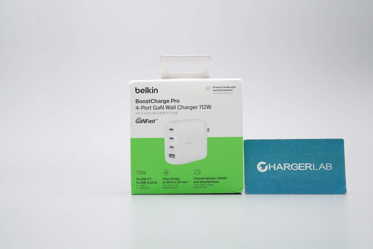
The front of the packaging features the Belkin brand, product name, appearance, and key selling points.
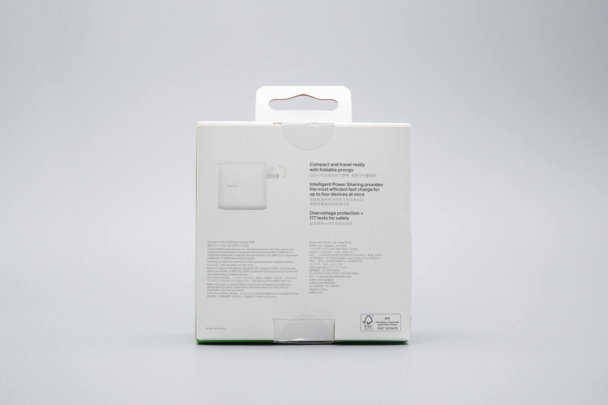
The back of the packaging displays the technical specifications.
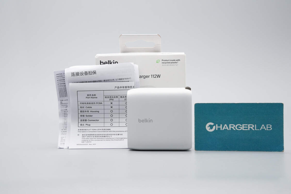
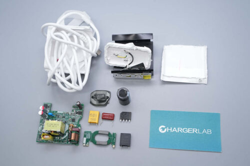
The package includes the charger, user manual, and other accessories.
The shell is made of recycled plastic with a matte finish.
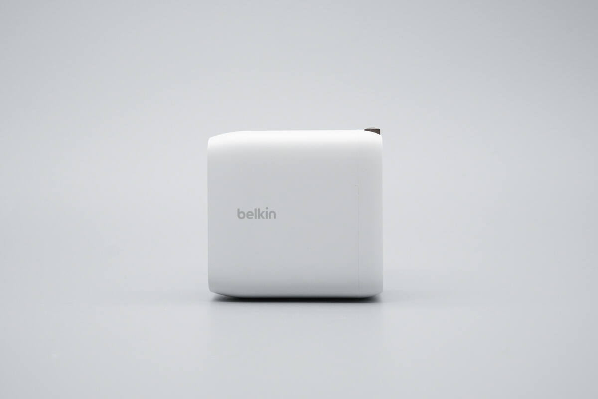
The front features the Belkin logo.
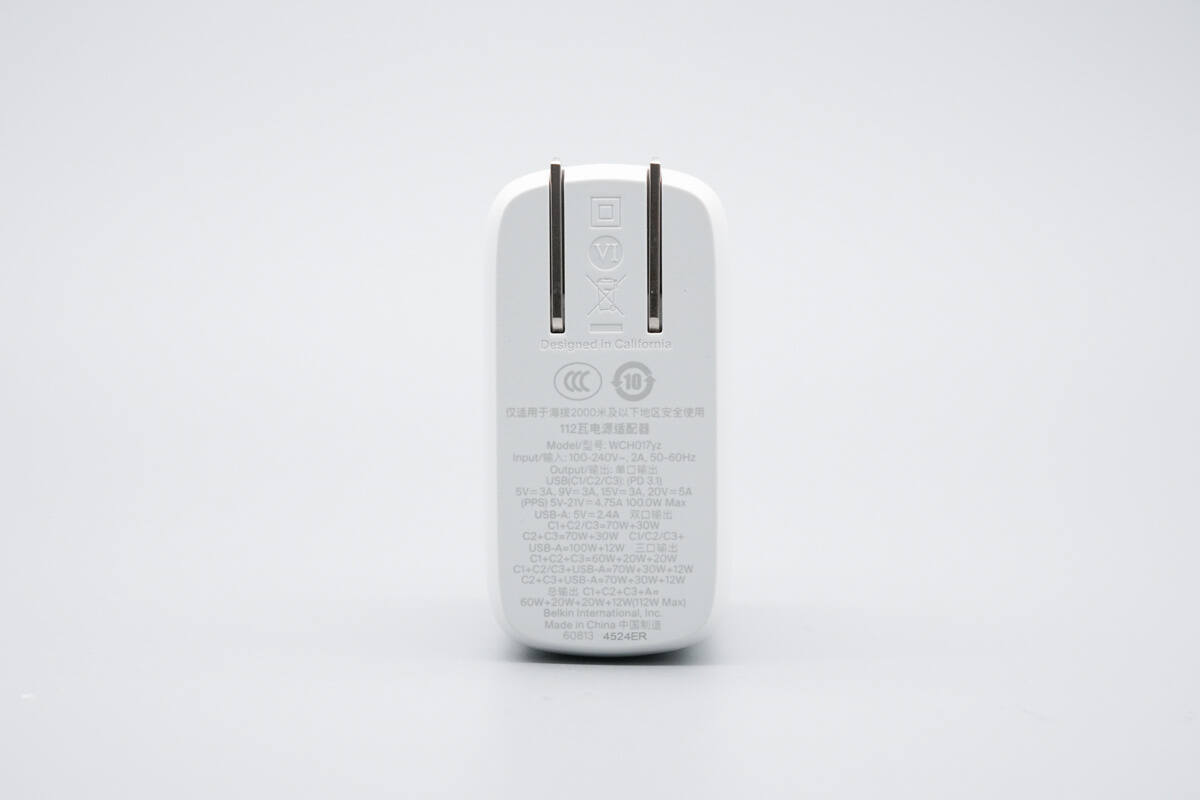
The input side of the shell displays the technical specifications.
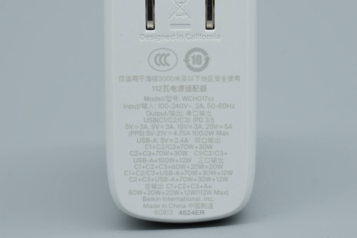
Model: WCH017yz
Input: 100-240V~50/60Hz 2A
Single-port output:
USB-C1/C2/C3: (PD 3.1) 5V3A, 9V3A, 15V3A, 20V5A
(PPS) 5-21V4.75A 100W Max
USB-A: 5V2.4A
Dual-port output:
C1 + C2/C3: 70W + 30W
C2 + C3: 70W + 30W
C1 + C2/C3 + USB-A: 100W + 12W
Triple-port output:
C1 + C2 + C3: 60W + 20W + 20W
C1 + C2 + C3 + USB-A: 70W + 30W + 12W
C2 + C3 + USB-A: 70W + 30W + 12W
Total output:
C1 + C2 + C3 + A = 60W + 20W + 20W + 12W (112W Max)
The charger has passed CCC certification and VI-level energy efficiency certification.
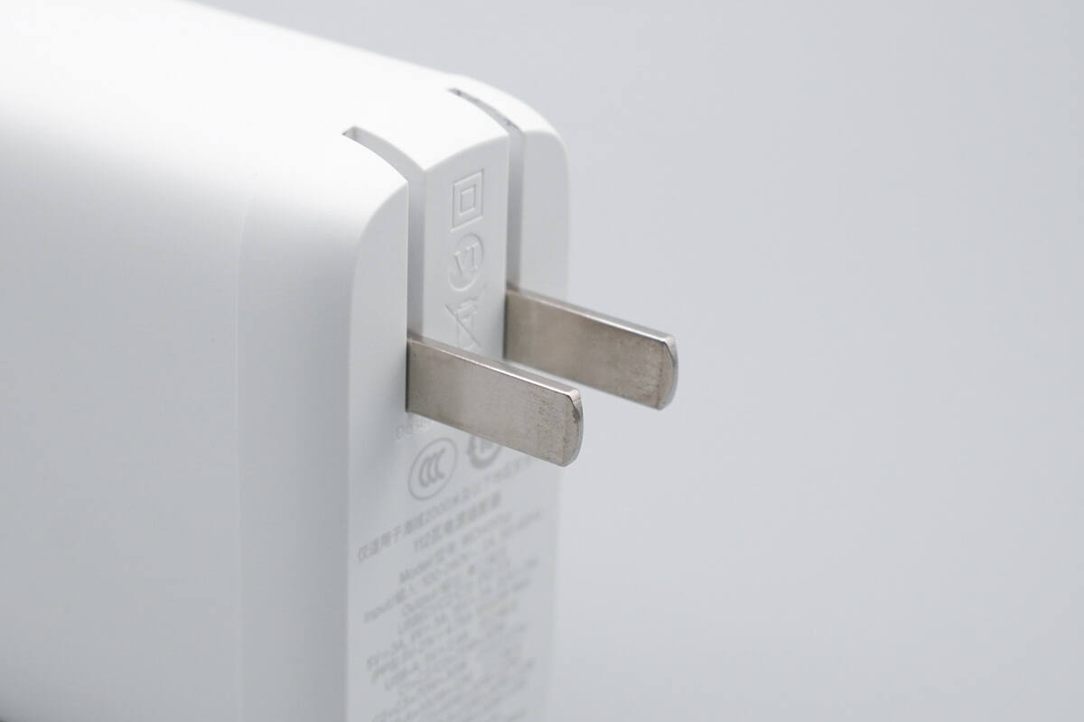
It is equipped with foldable prongs.
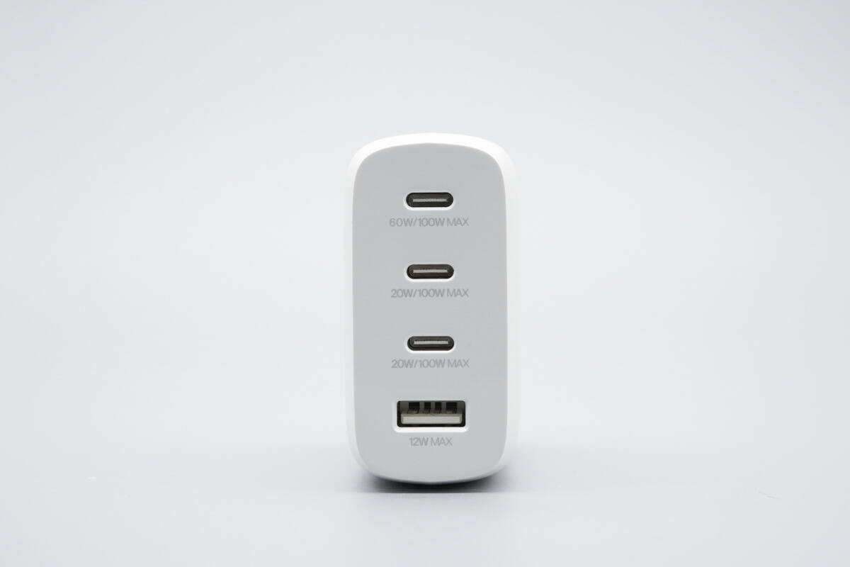
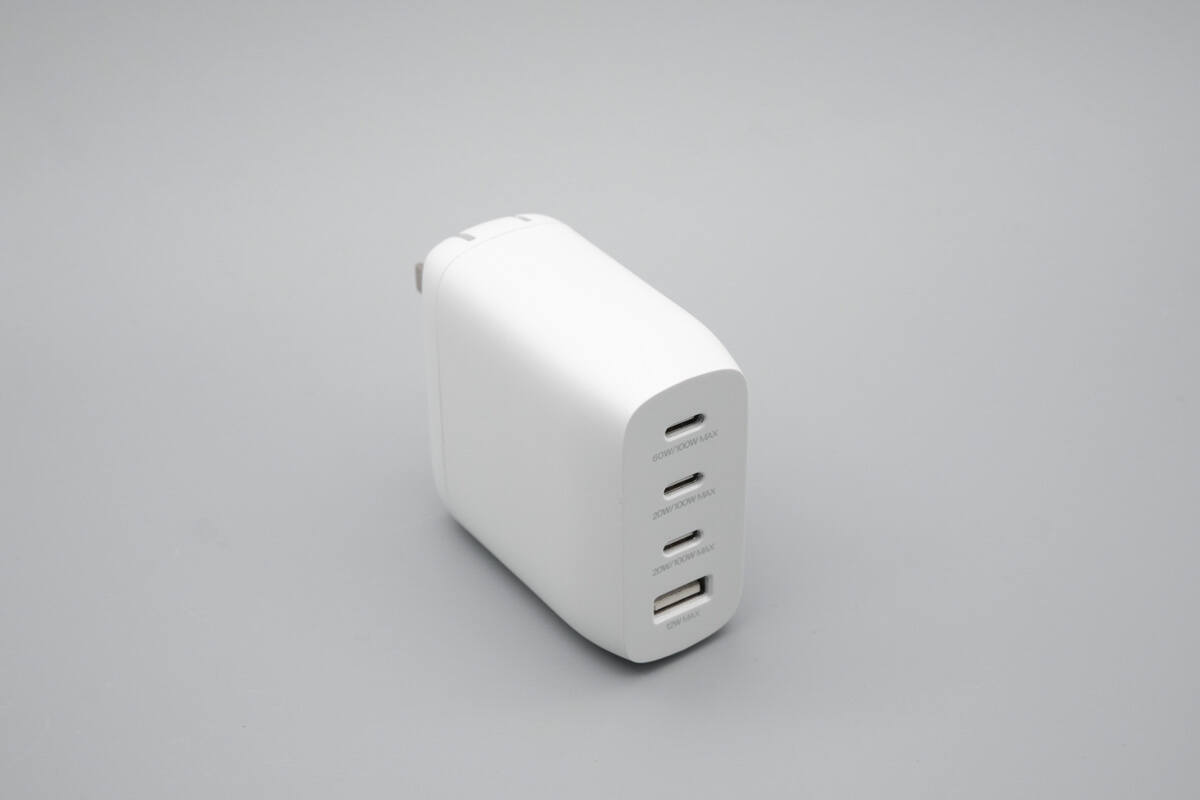
It is equipped with 3 USB-C ports and 1 USB-A port.
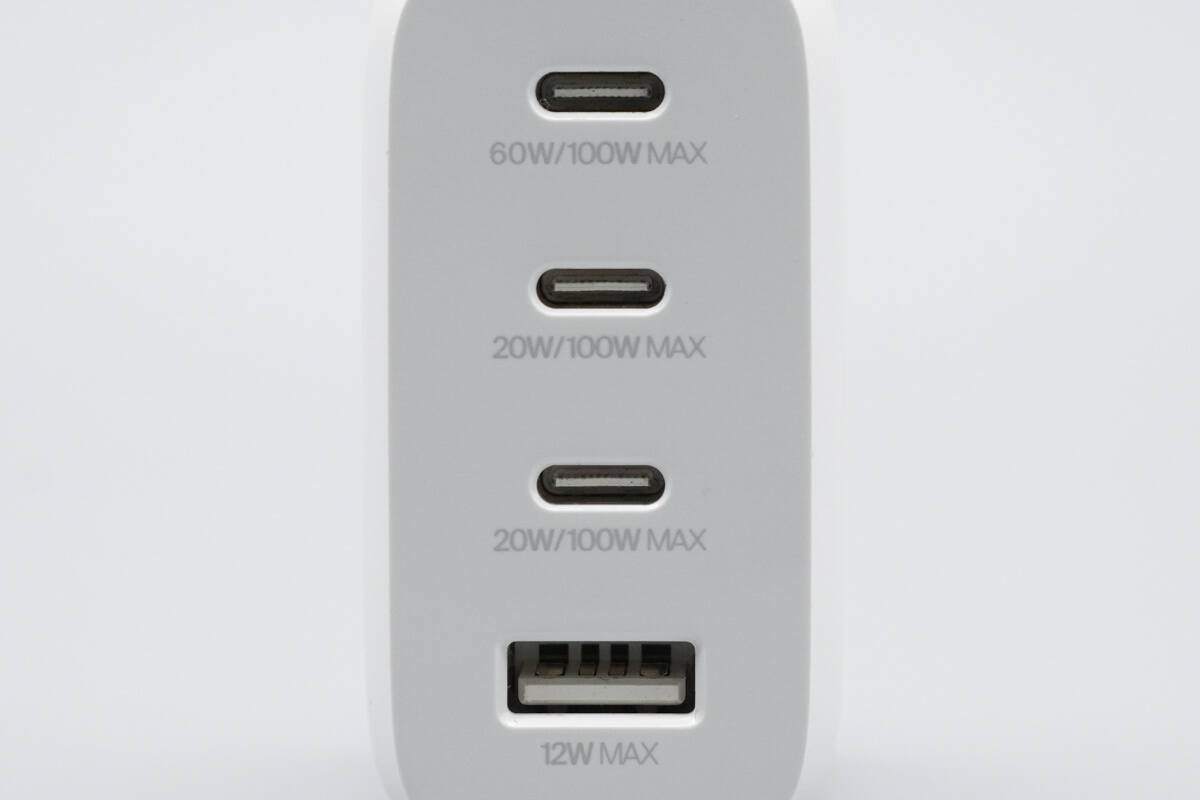
Power output parameters for both single and multi-port combinations are printed next to all four ports.
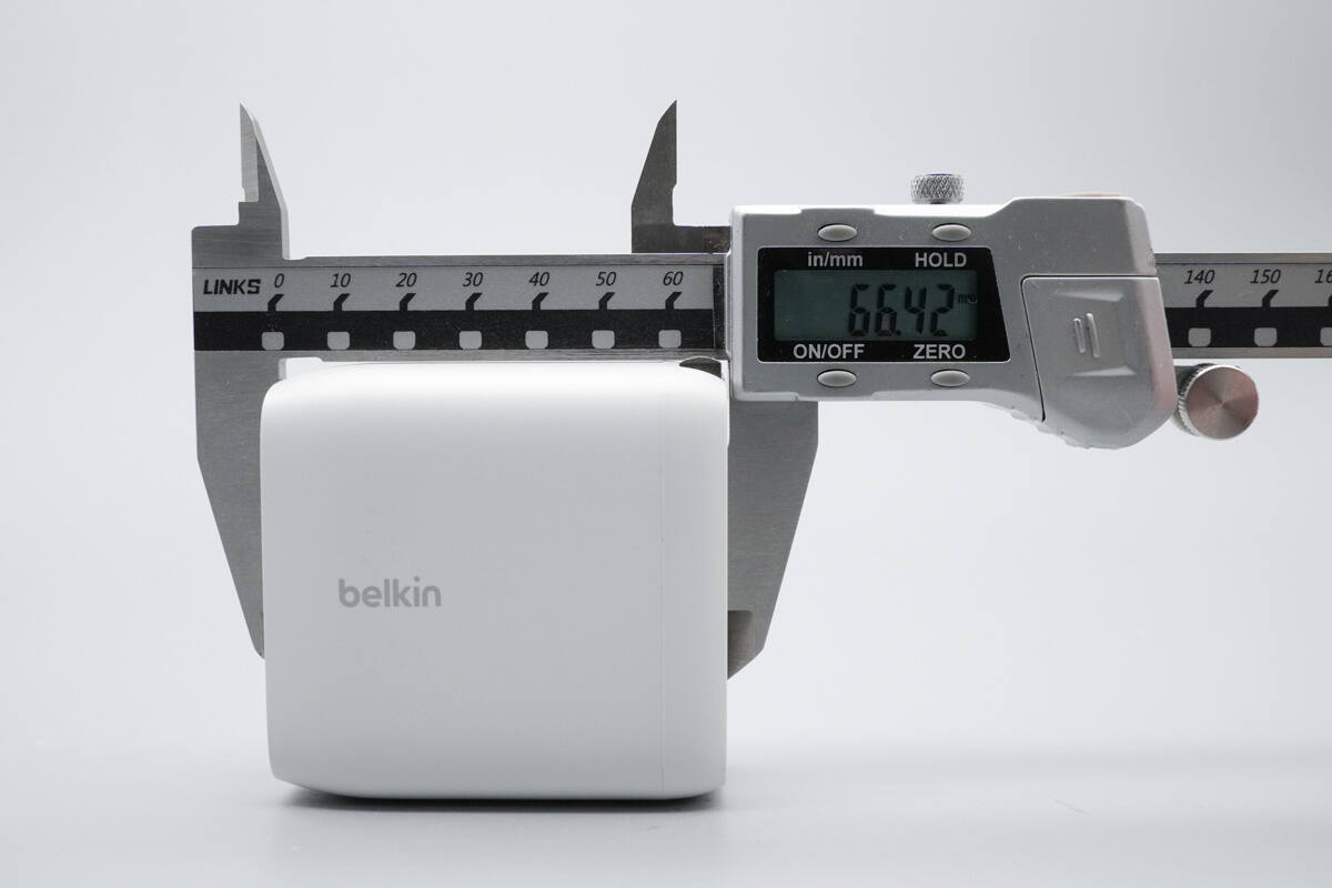
The length of the charger is about 66.42 mm (2.61 inches).
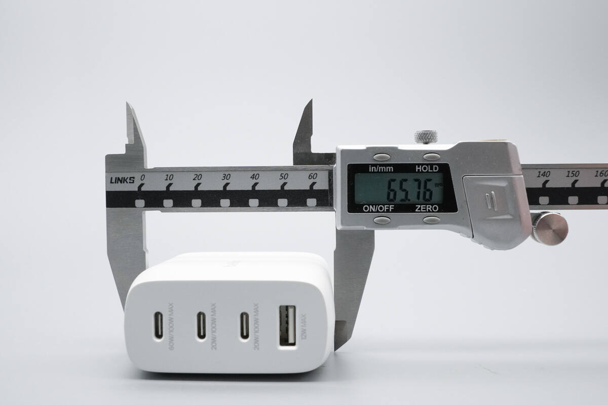
The width is about 65.76 mm (2.59 inches).
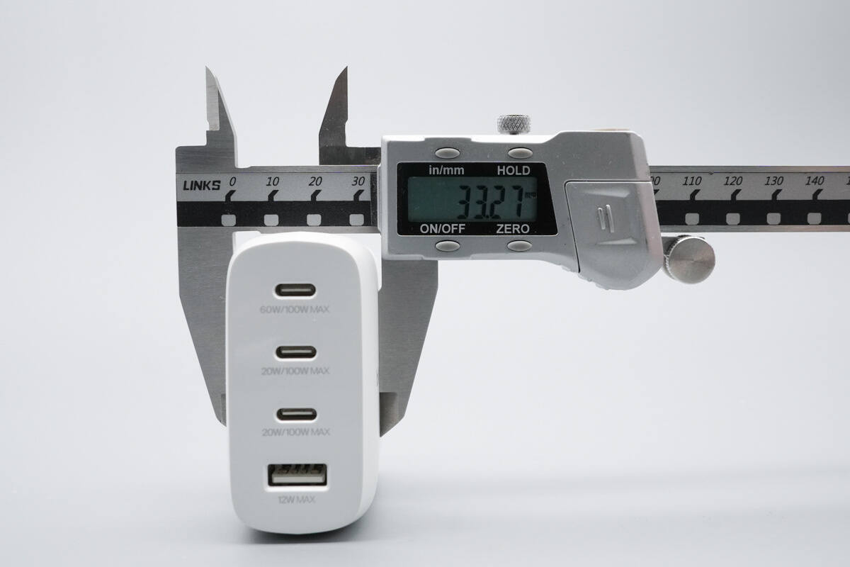
The thickness is about 33.27 mm (1.31 inches).
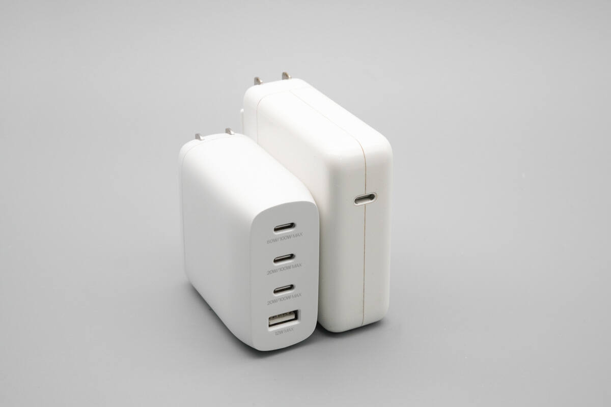
Its size is slightly smaller than that of the Apple 96W charger.
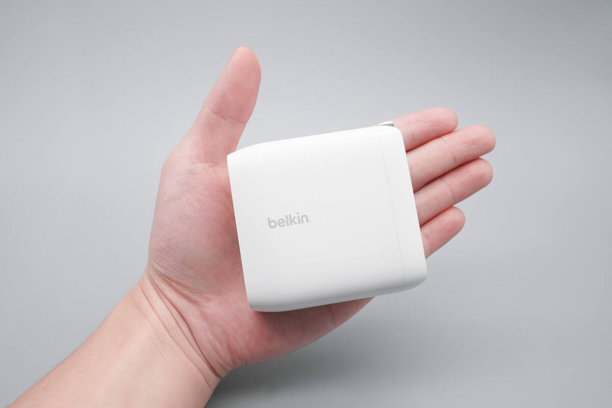
That's how big it is on the hand.
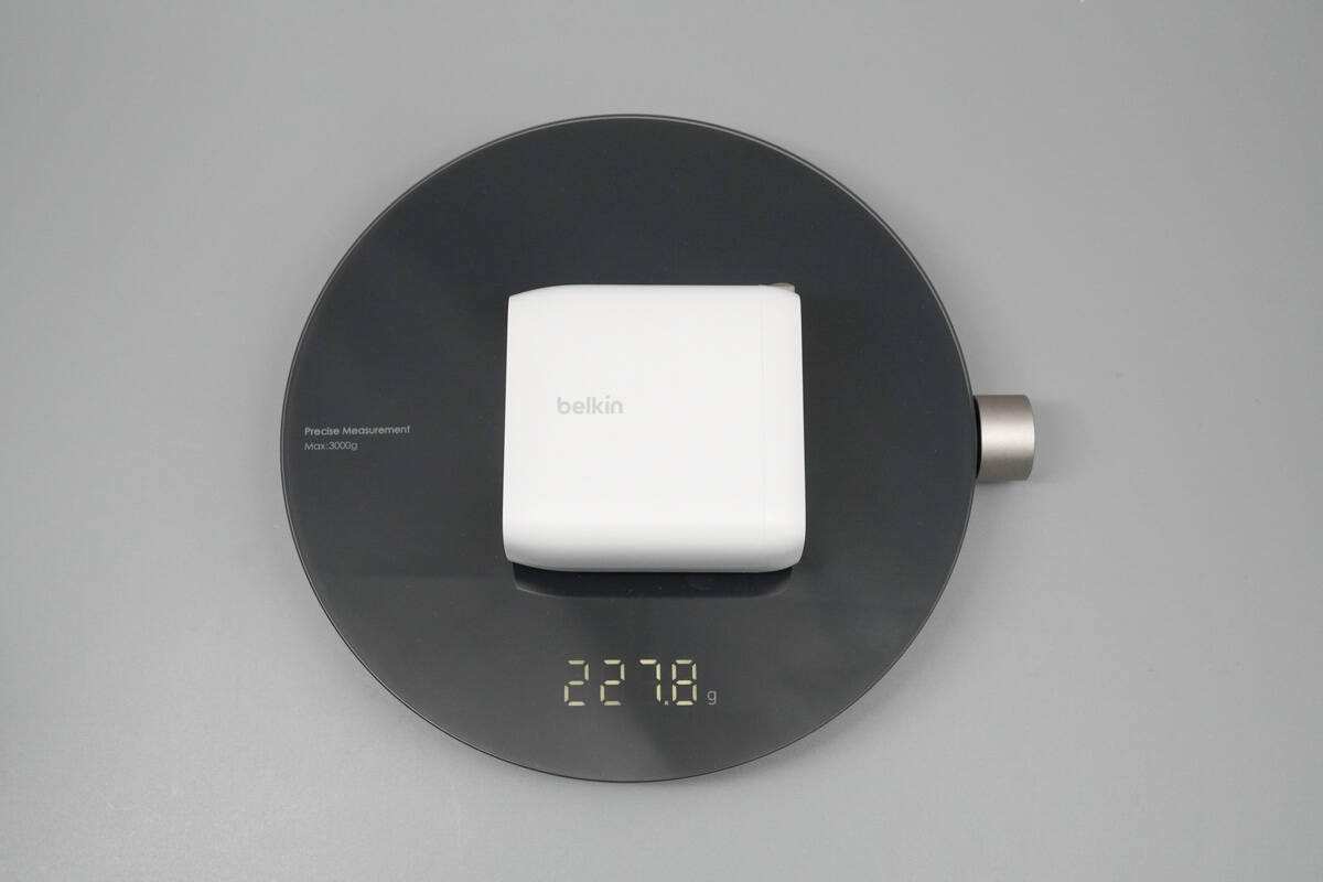
The weight is about 228 g (8.042 oz).
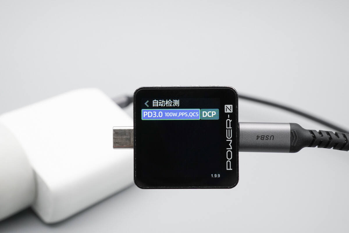
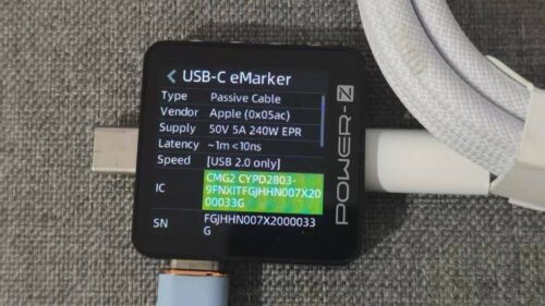
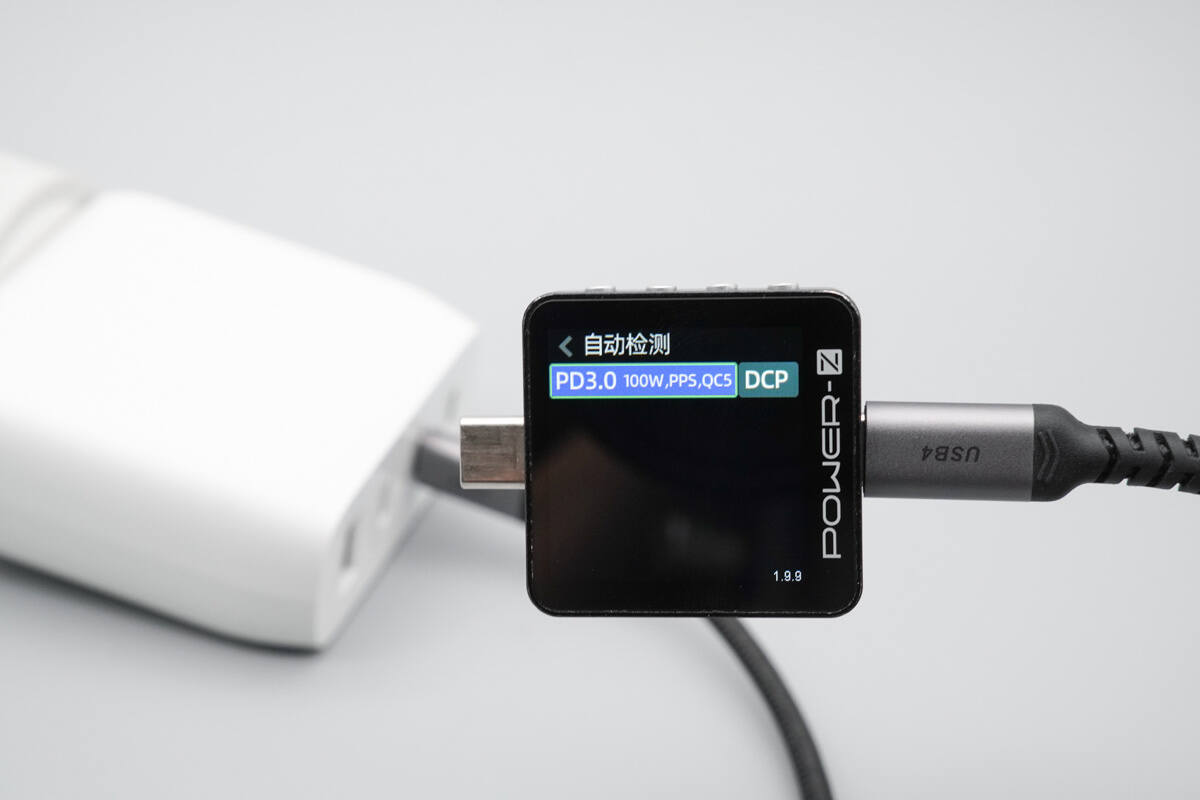
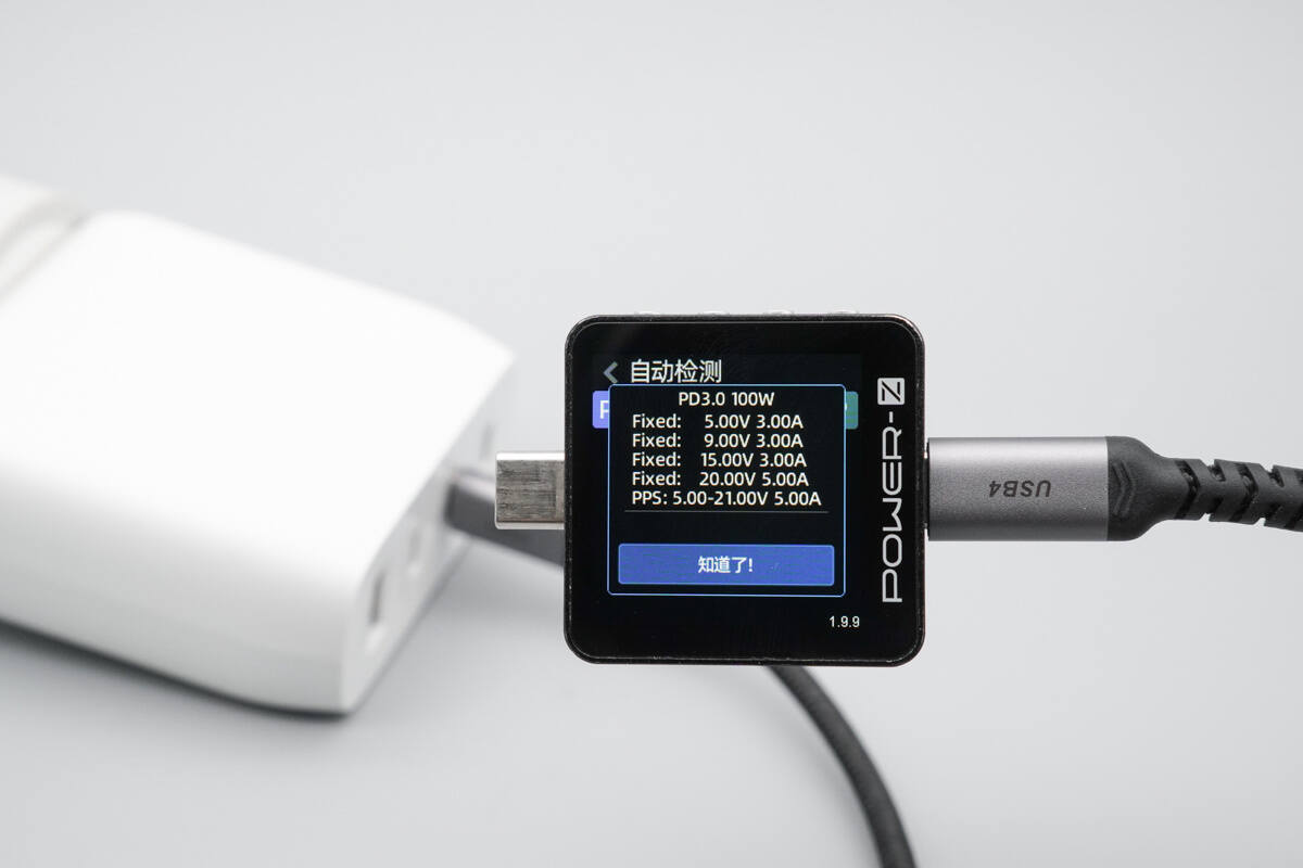
ChargerLAB POWER-Z KM003C shows that the USB-C1 port supports PD3.0, PPS, QC5, and DCP charging protocols.
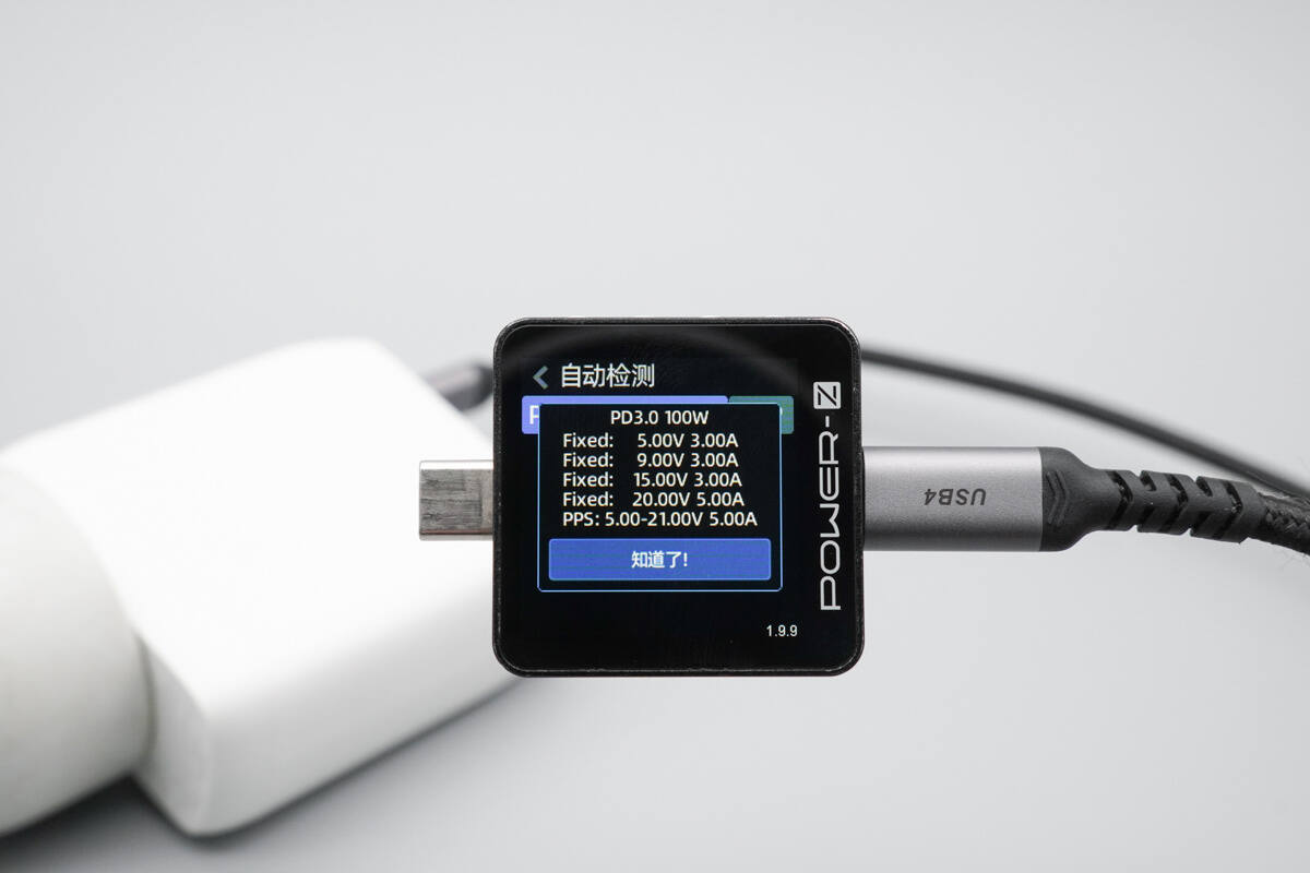
It features four fixed PDOs of 5V3A, 9V3A, 15V3A, 20V5A, along with a 5-21V5A PPS voltage range.
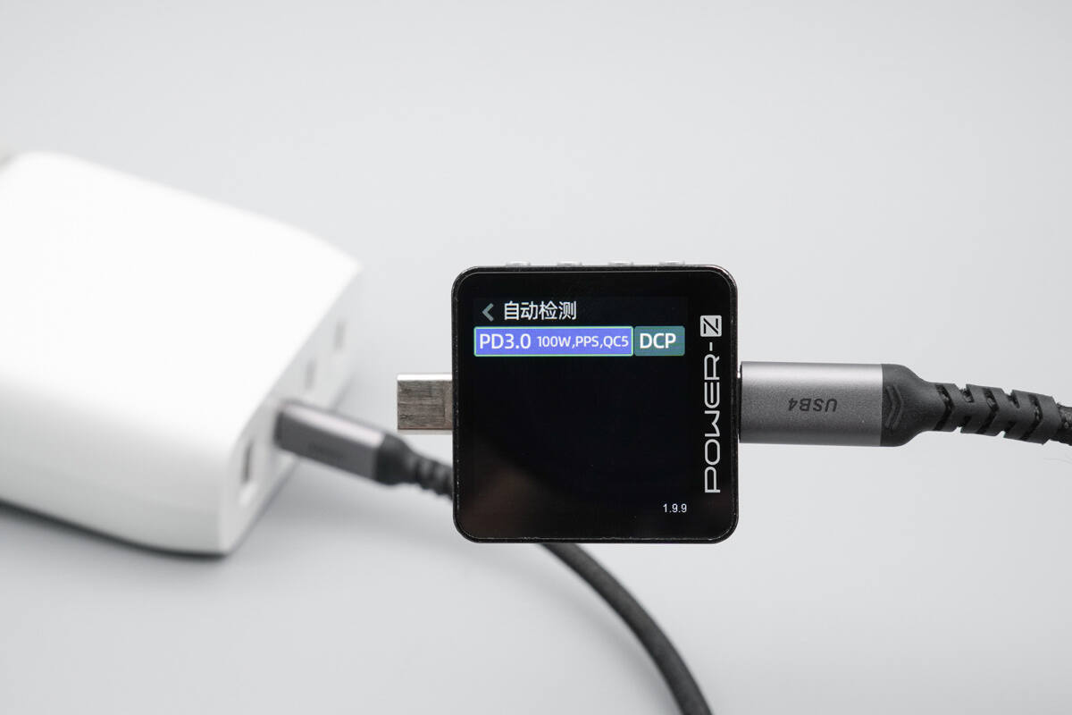
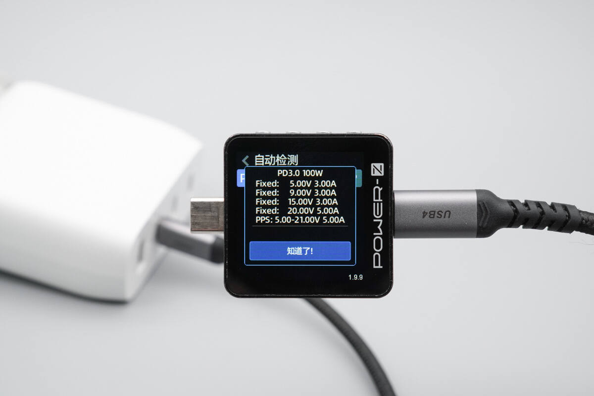
The protocols compatible with the USB-C2 port are the same as those of the USB-C1 port.
The PDO messages are also the same.
The protocols compatible with the USB-C3 port are the same as those of the USB-C1 port.
The PDO messages are also the same.
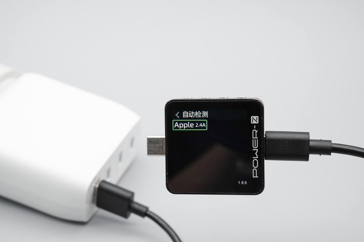
The USB-A port supports the Apple 2.4A charging protocol.
Teardown
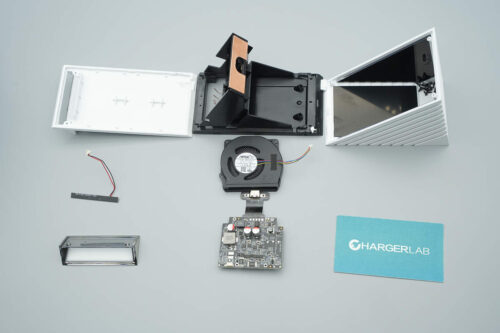
Next, let's take it apart to see its internal components and structure.

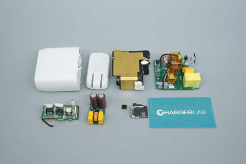
Upon opening the input side of the shell, it is filled with a large amount of thermal paste.
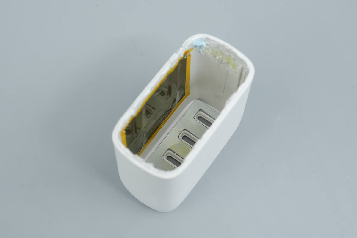
After removing the PCBA module, an insulating thermal pad is attached to the inner side of the shell.
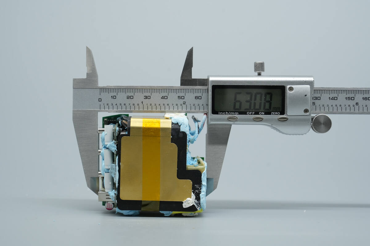
The length of the PCBA module is about 63.08 mm (2.48 inches).
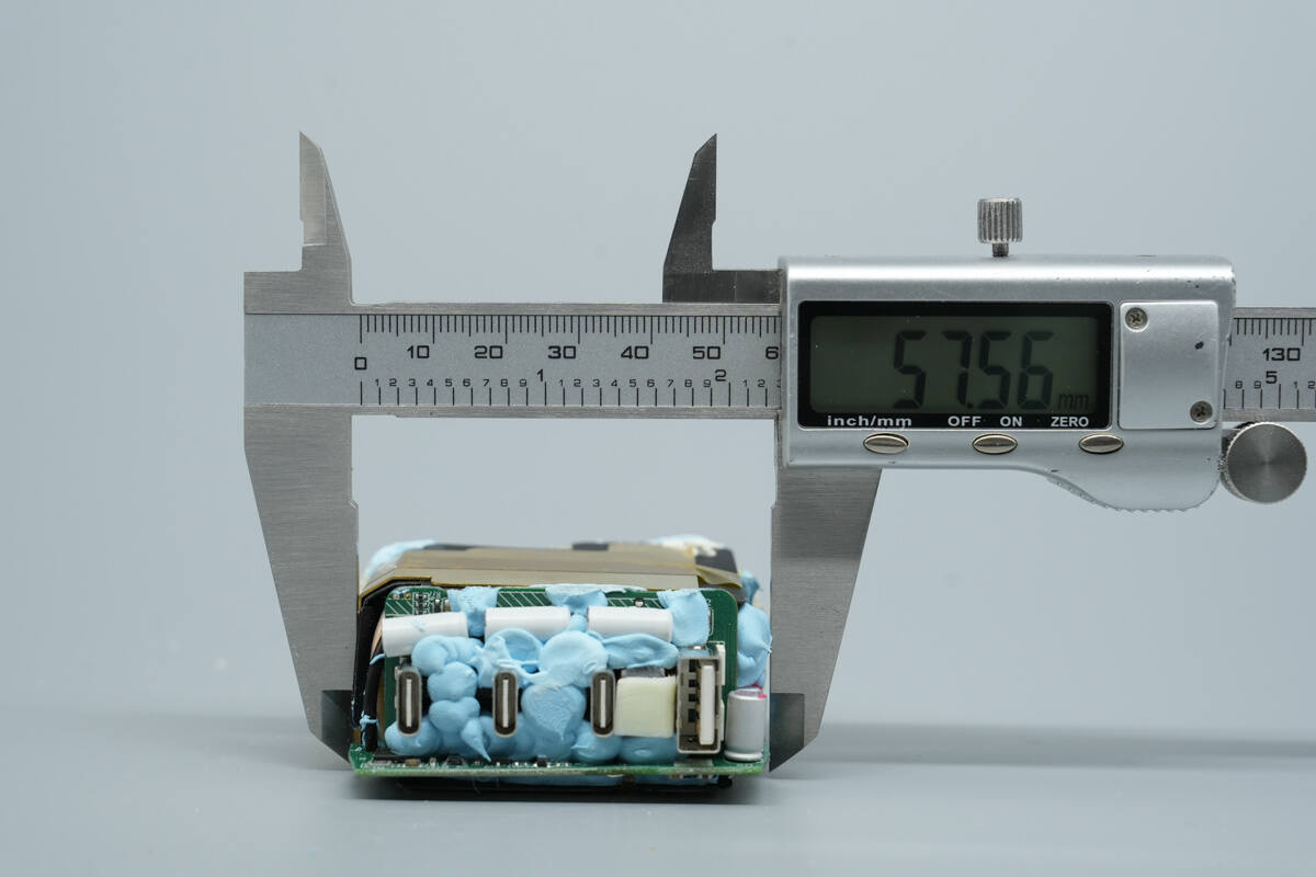
The width is about 57.56 mm (2.27 inches).
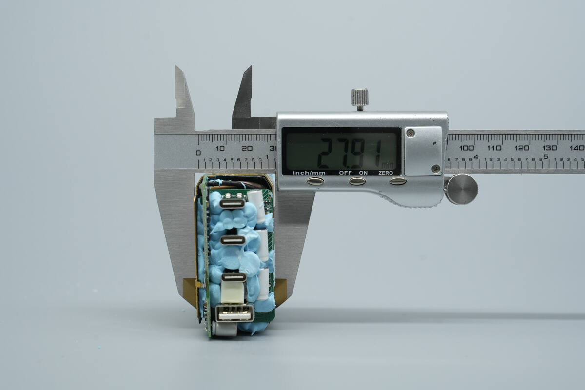
The thickness is about 27.91 mm (1.099 inches).
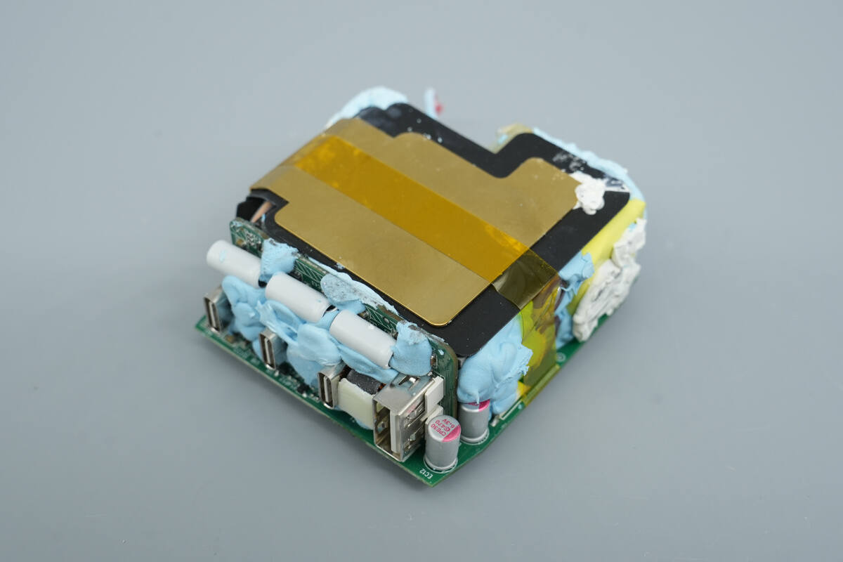
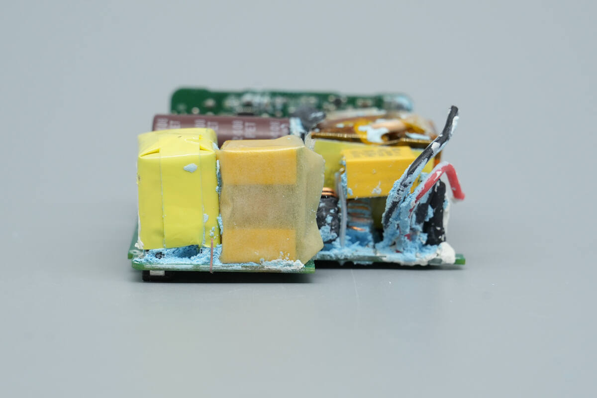
The PCBA module is covered with a Mylar sheet and a single-piece copper sheet and is secured with tape.

After removing the heat sink, the PCBA module is covered with a large amount of blue thermal paste. The backside of the small PCB at the output end also has a thermal pad.
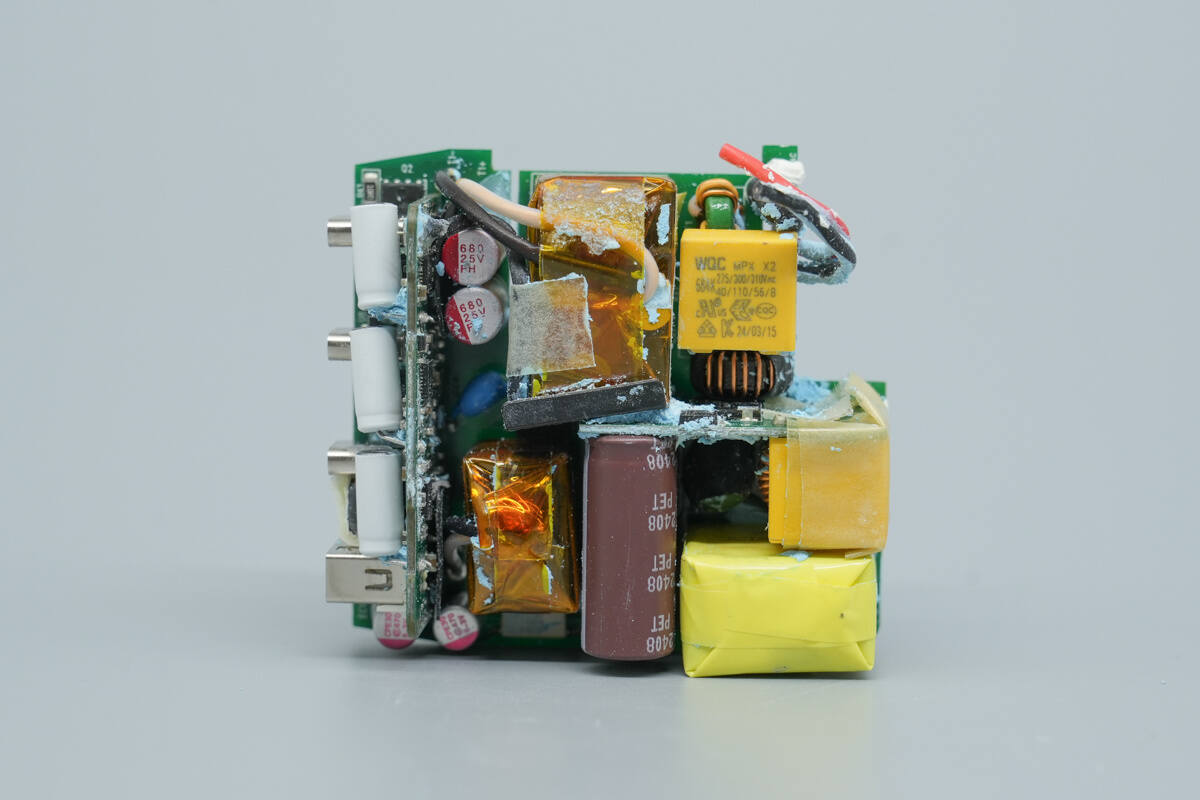
After cleaning off the blue thermal paste, several small PCBs are soldered onto the module.
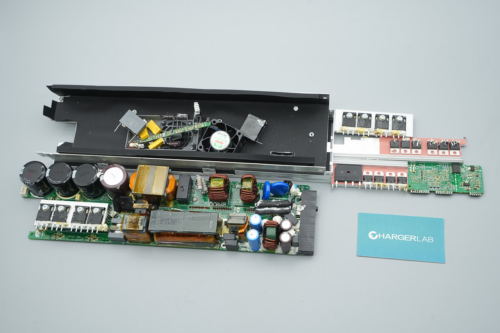
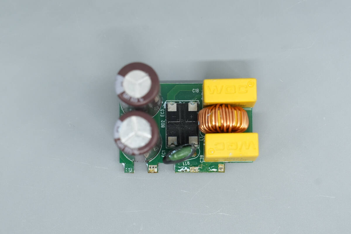
The backside of the PCBA features a PFC boost circuit and two switch-mode power supply circuits.
The front end of the PCBA module contains components such as a fuse, common mode choke, and safety X2 capacitors.
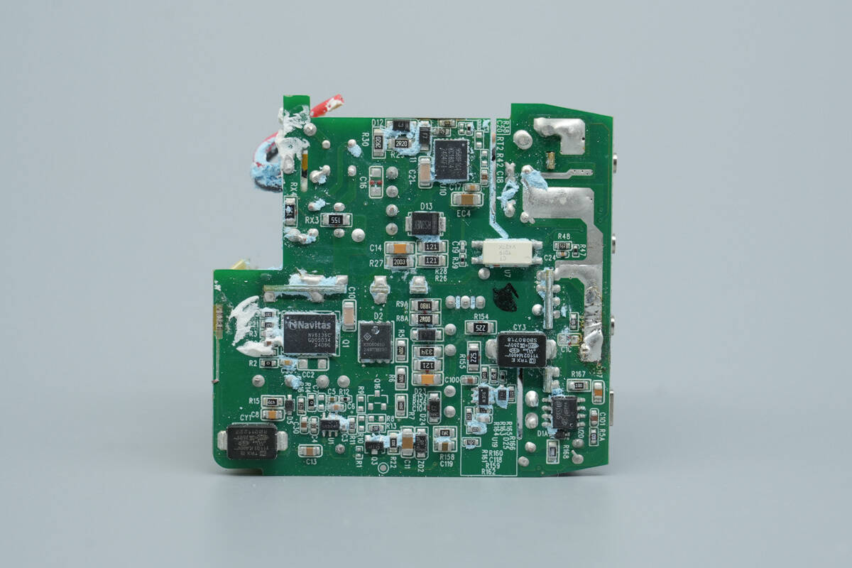
After removing the small PCB, the front side features components such as an NTC thermistor, a bridge rectifier, film capacitors, a filter inductor, and electrolytic capacitors.
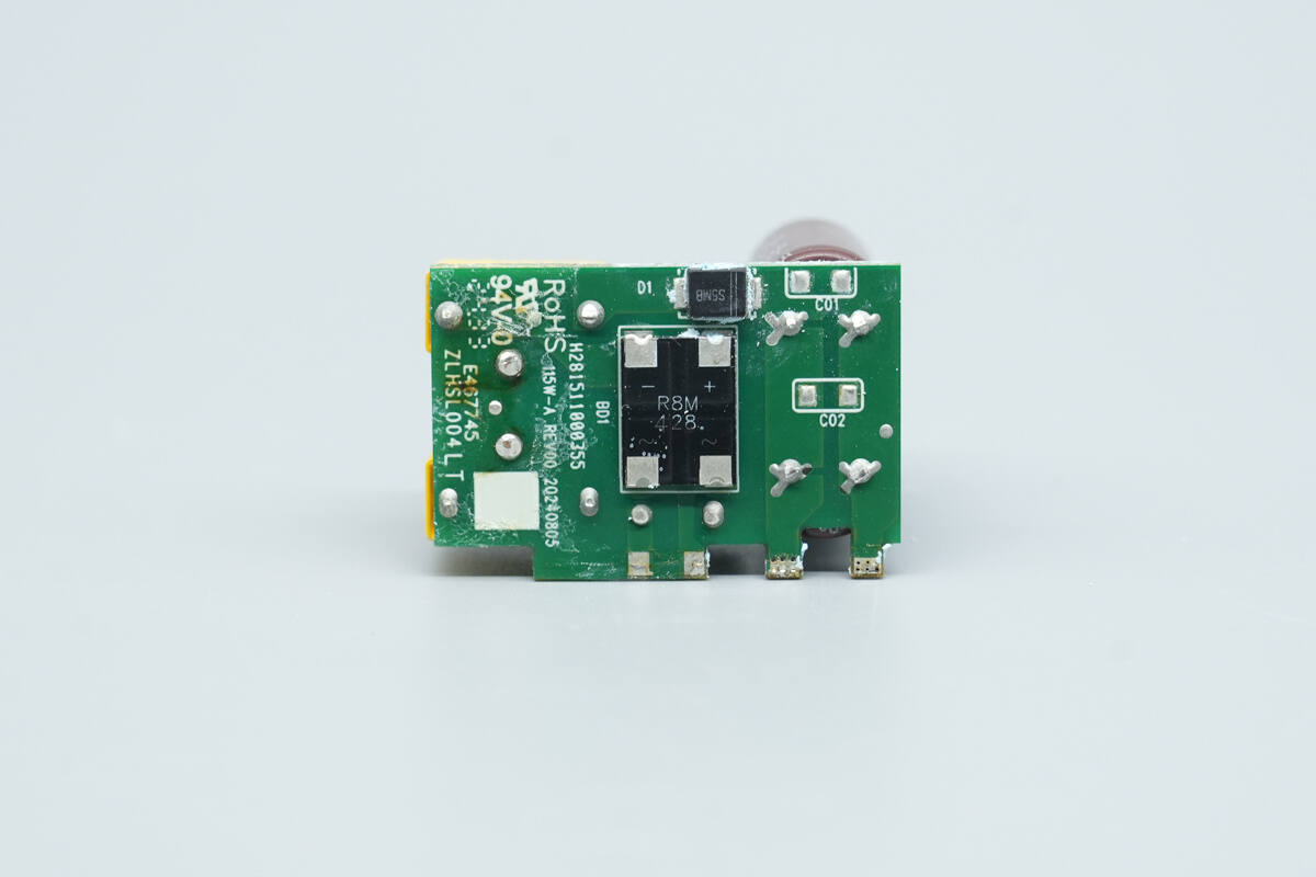
The backside has another bridge rectifier.
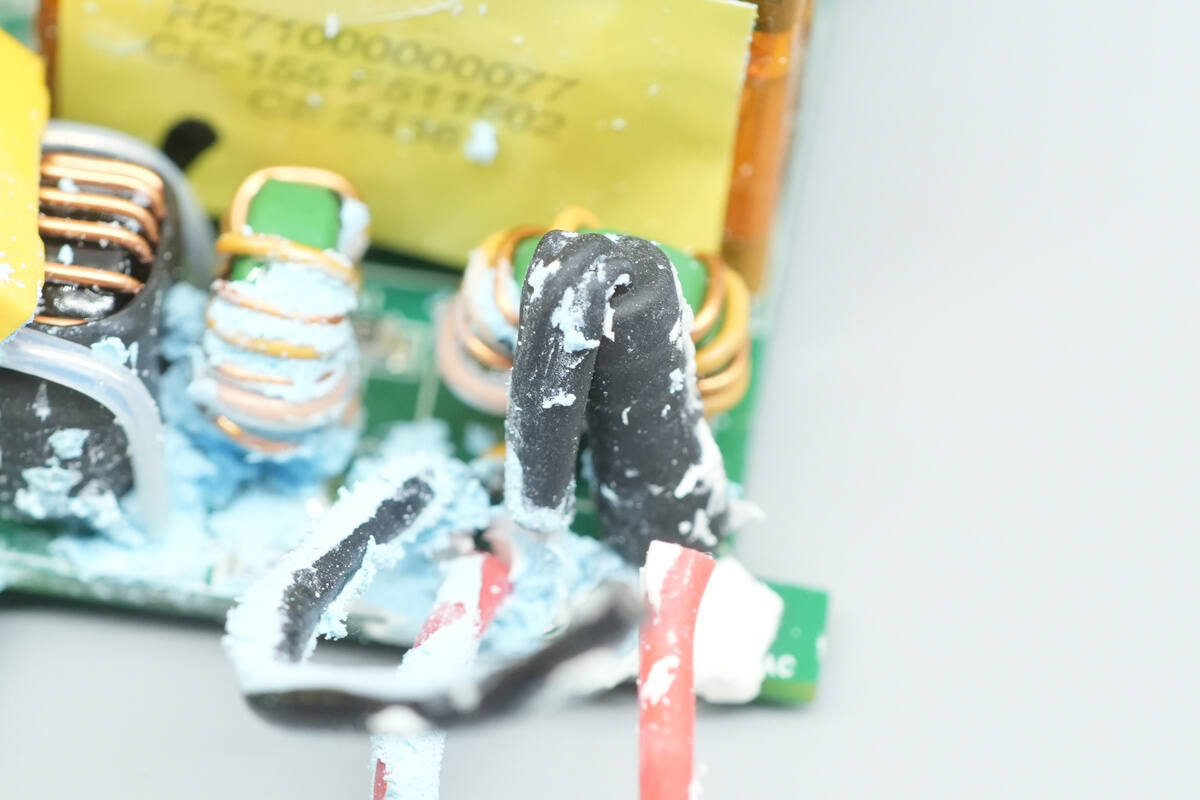
The fuse is insulated with a heat shrink tube.
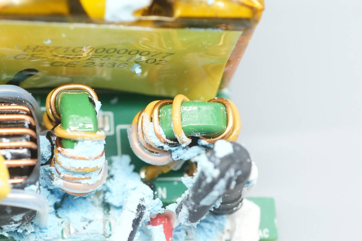
The common mode choke is used to filter out EMI.
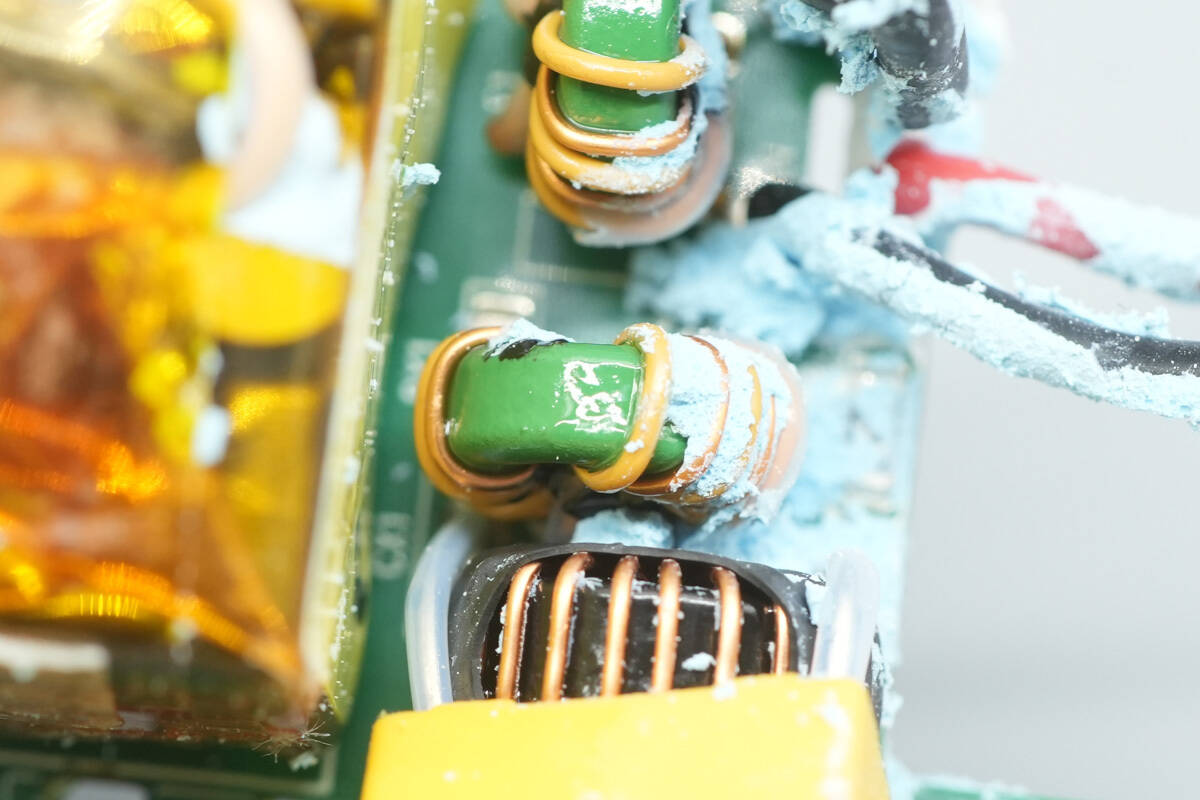
A close-up of the other common mode choke.
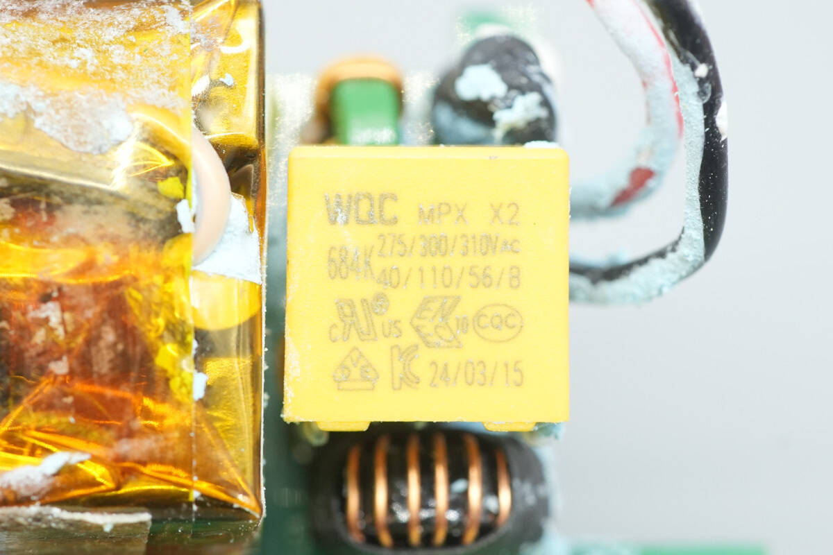
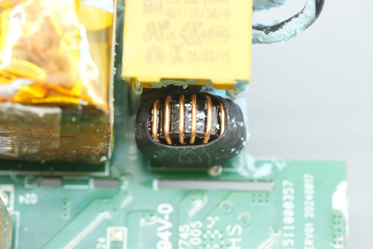
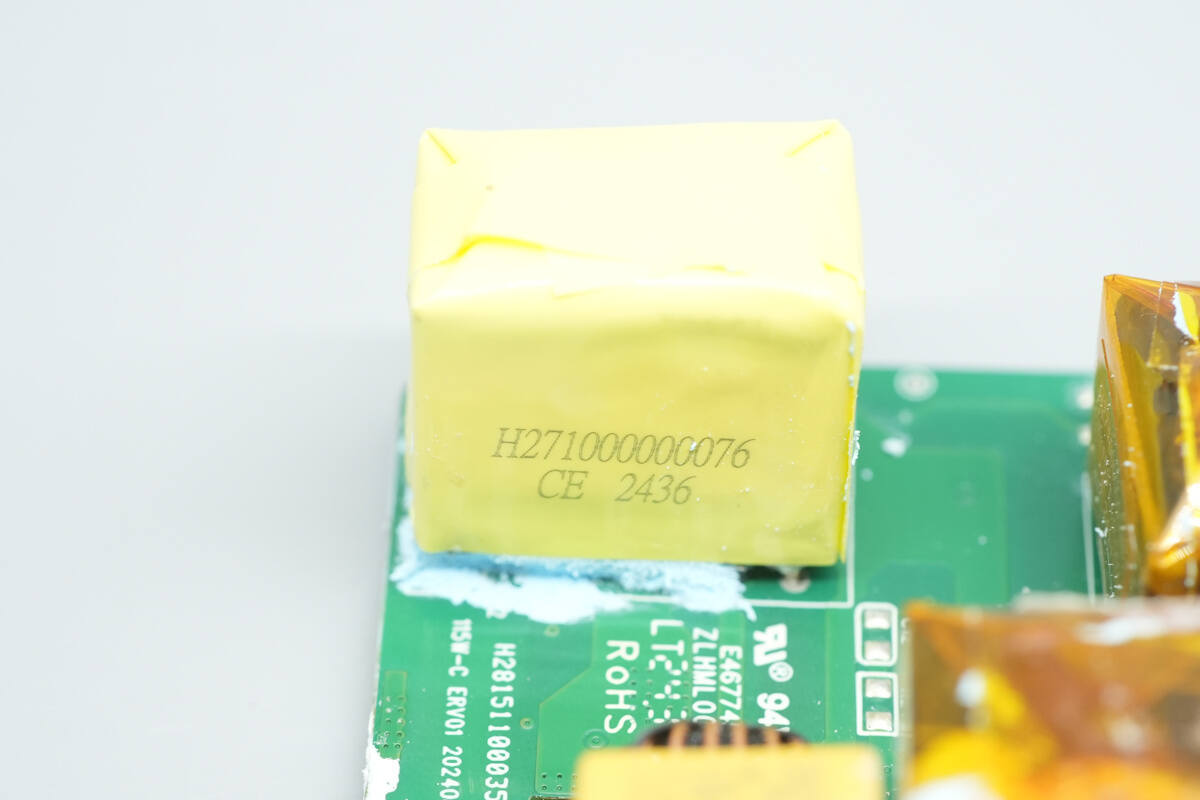
The safety X2 capacitor is from WQC, with a capacitance of 0.68µF.
The filter inductor is insulated with a heat shrink tube.
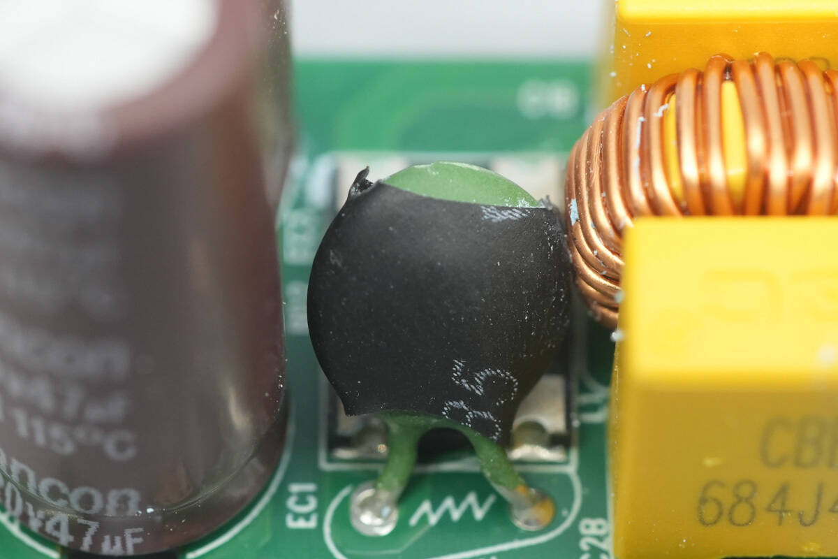
The NTC thermistor is used to suppress inrush current at power-on and is insulated with a heat shrink tube.
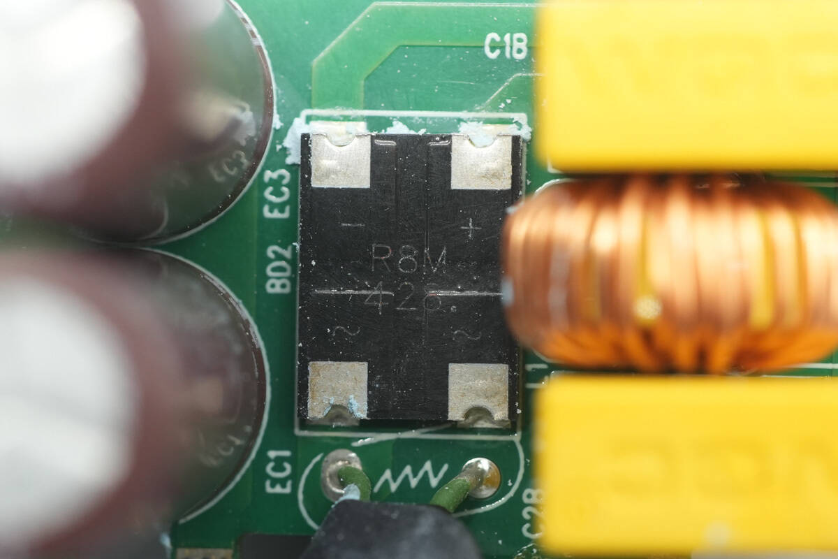
A close-up of the R8M428 bridge rectifier.
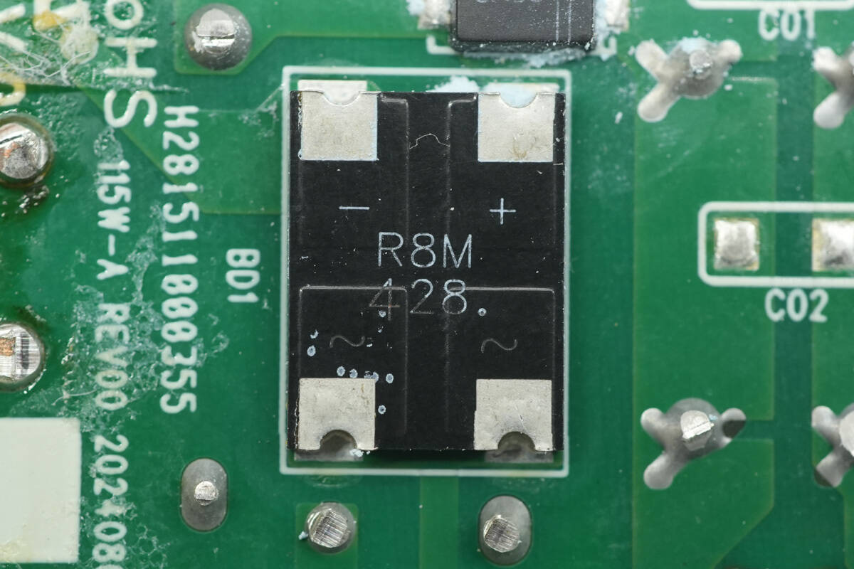
A close-up of the other bridge rectifier.
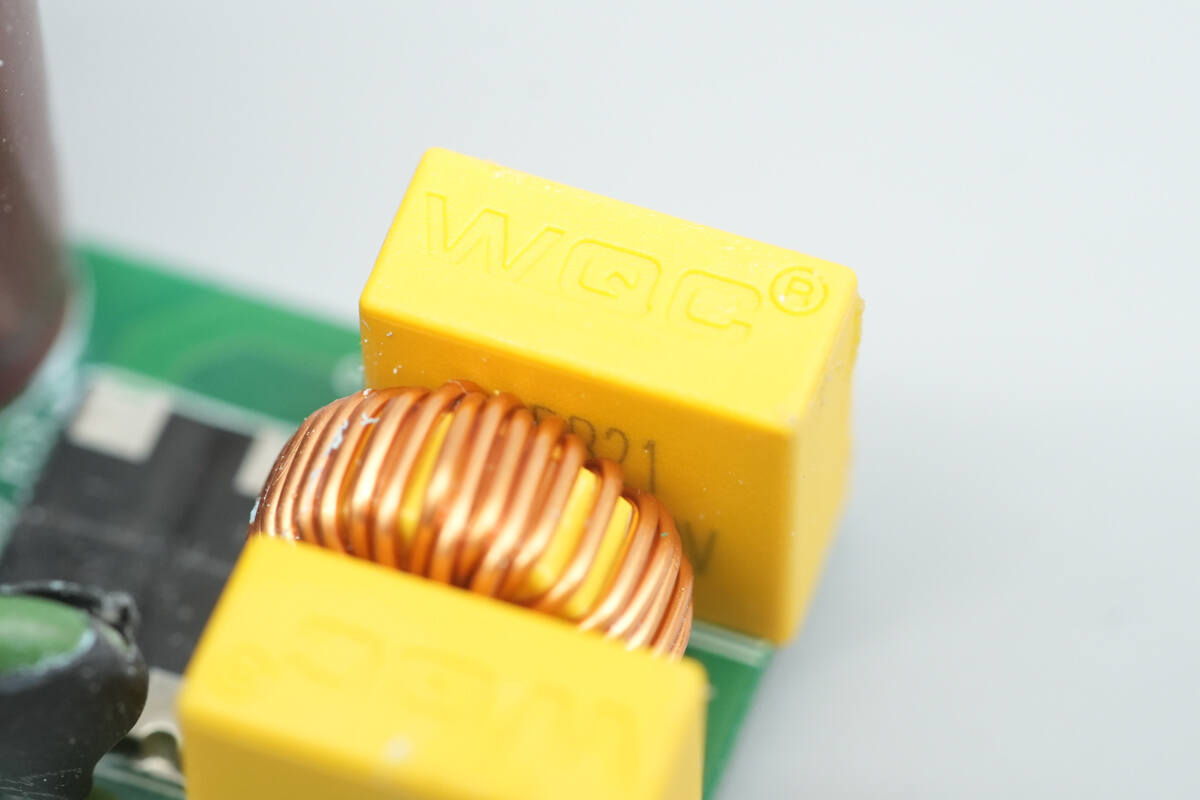
The two CBB21 film capacitors are also from WQC.
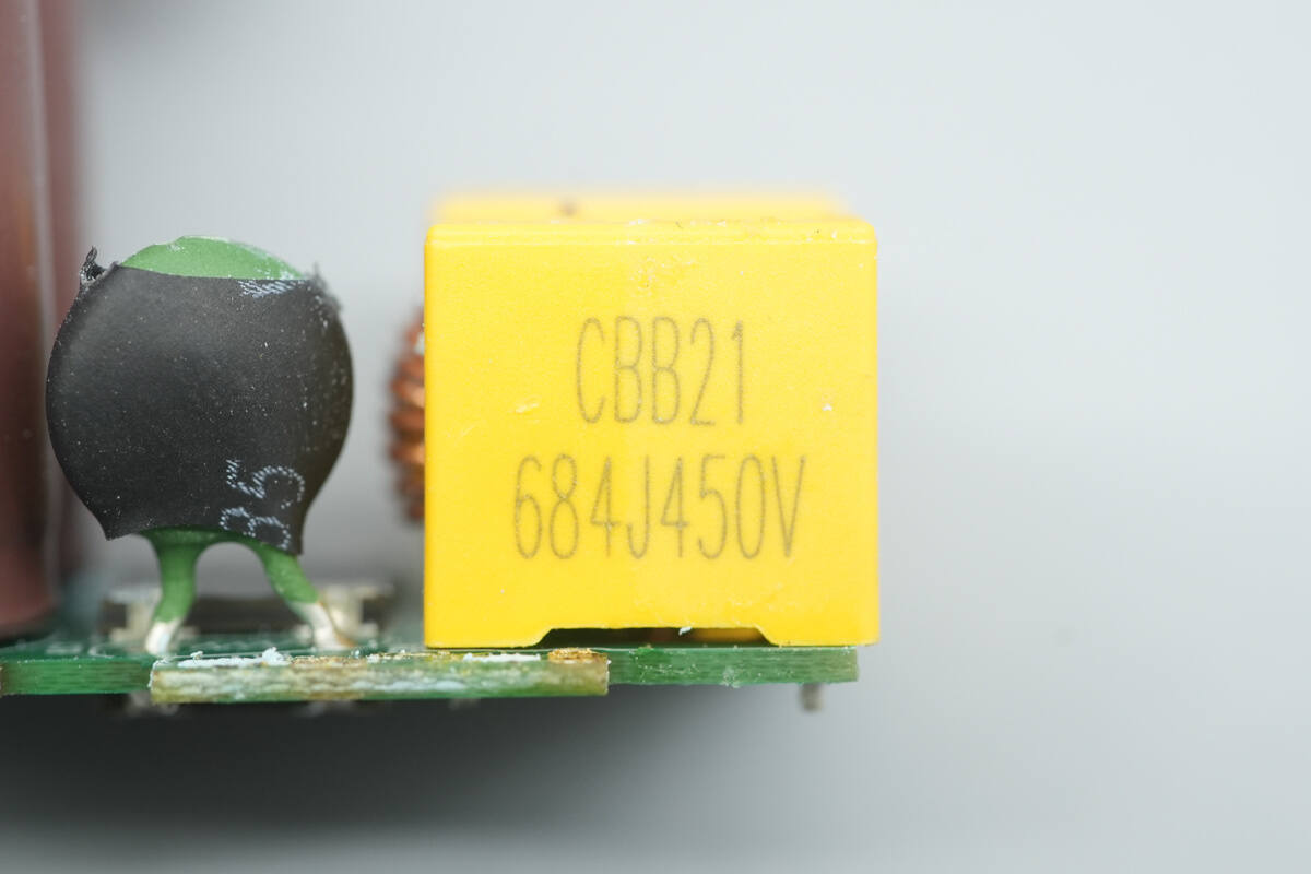
The film capacitors have a specification of 0.68µF, 450V.
A close-up of the filter inductor.
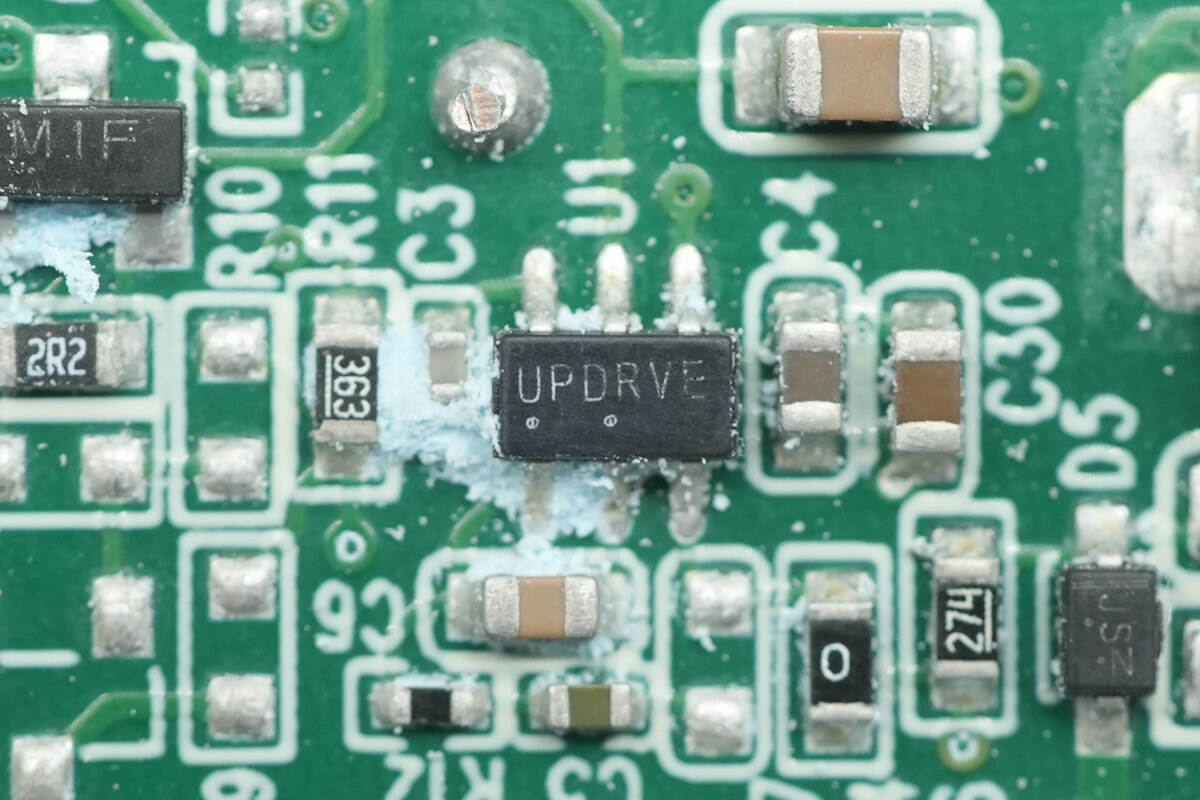
The PFC controller is from Onsemi, marked with UPD, and the model is NCP1623. It is based on the innovative Valley Synchronous Frequency Foldback (VSFF) method. VSFF maximizes efficiency under both nominal and light load conditions, operating in critical mode under heavy load and in discontinuous conduction mode (DCM) under light load, while supporting valley switching to improve efficiency.
The NCP1623 supports operation in both critical mode and discontinuous conduction mode, with valley-synchronous frequency foldback enhancing efficiency under nominal and light loads, and achieving a good power factor at low switching frequencies.
The PFC MOSFET is from Navitas, model NV6136C. This is a highly integrated GaN power chip with an integrated driver and high-precision, lossless current sensing circuitry that eliminates the loss associated with sampling resistors. The NV6136C features a 170mΩ Rds(on), a 700V-rated GaN FET, supports a 2MHz switching frequency, and comes in a 6x8mm QFN package, saving space.
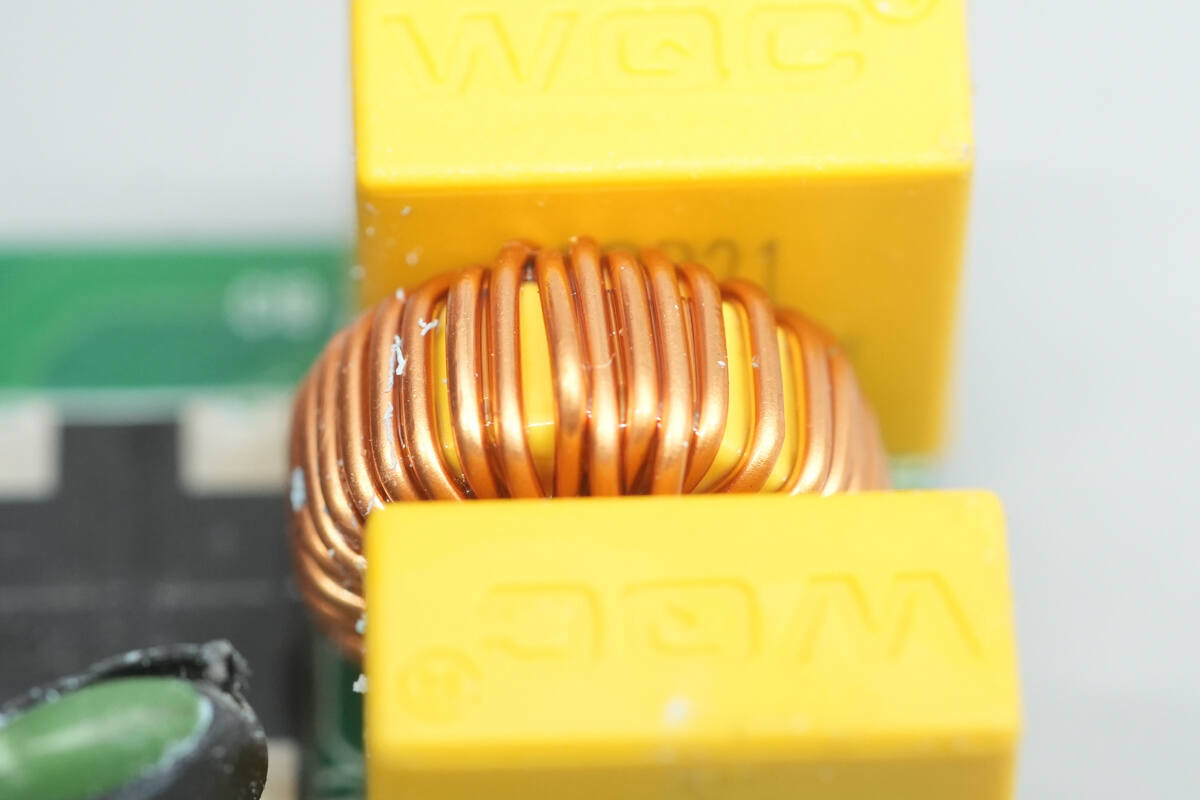
A close-up of the PFC boost inductor.
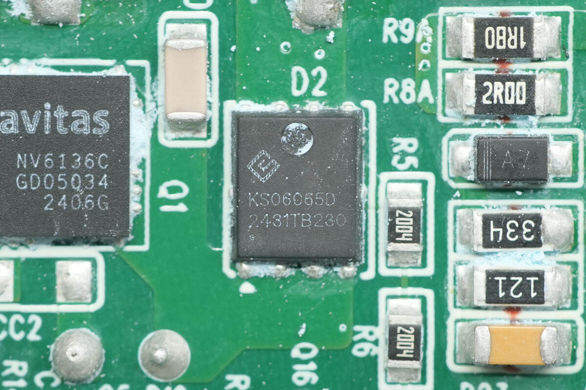
The PFC rectifier is from SGKS, model KS06065D. It is a silicon carbide Schottky diode with a specification of 650V, 6A, and comes in a PDFN 5x6 package.
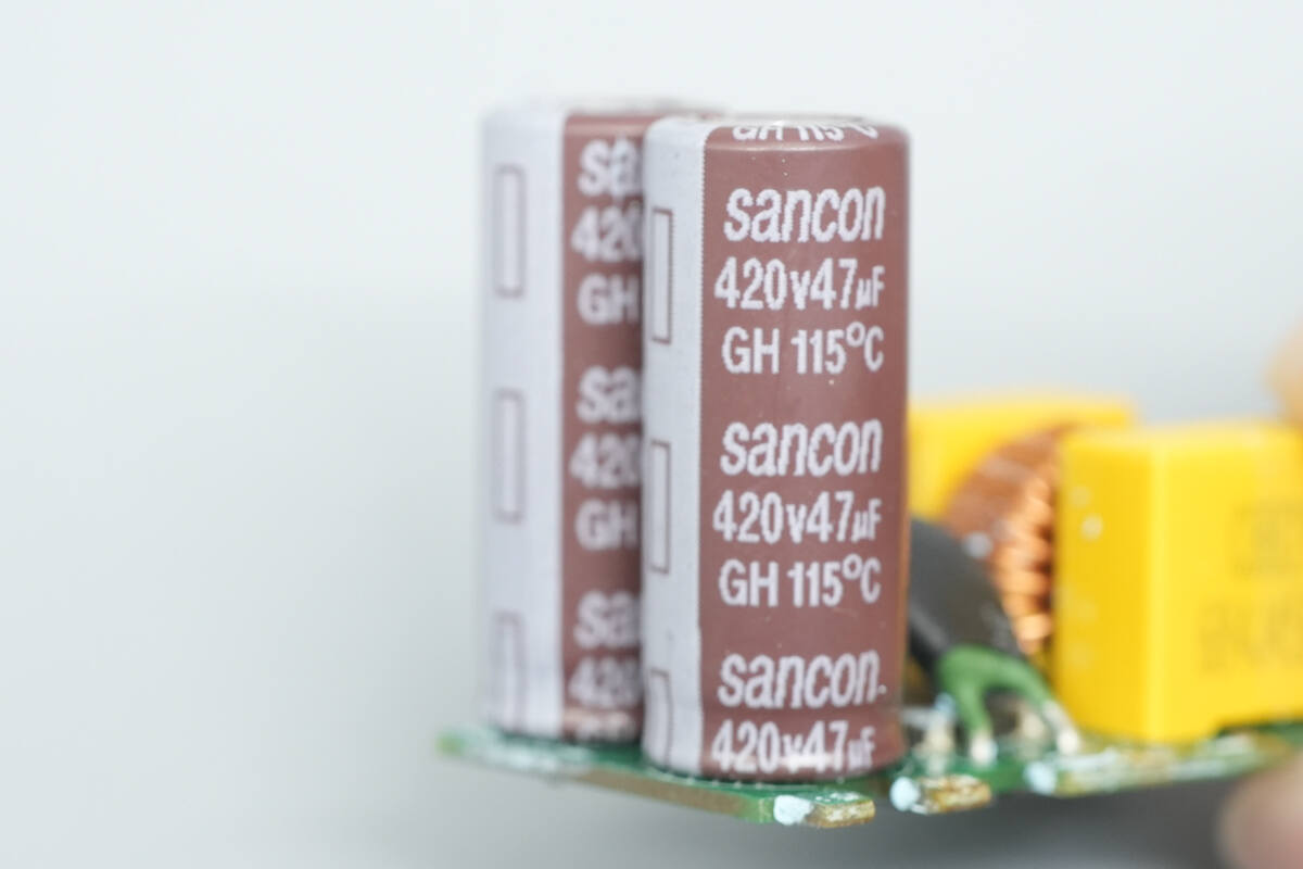
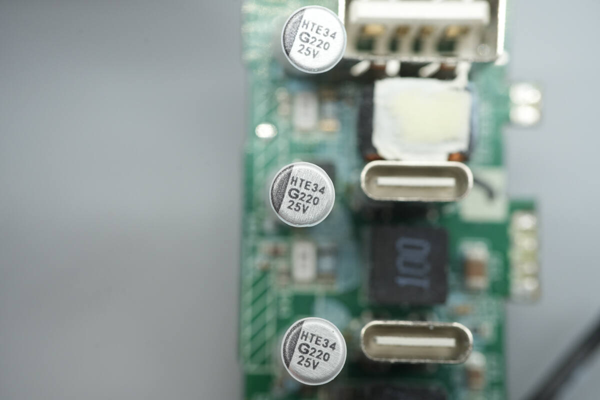
The high-voltage filter electrolytic capacitors are from Sancon, with a specification of 420V, 47µF.
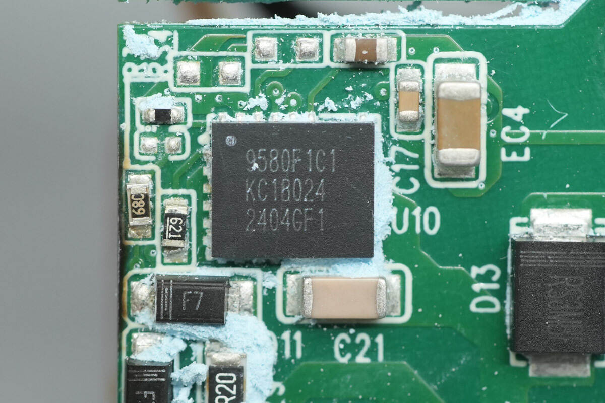
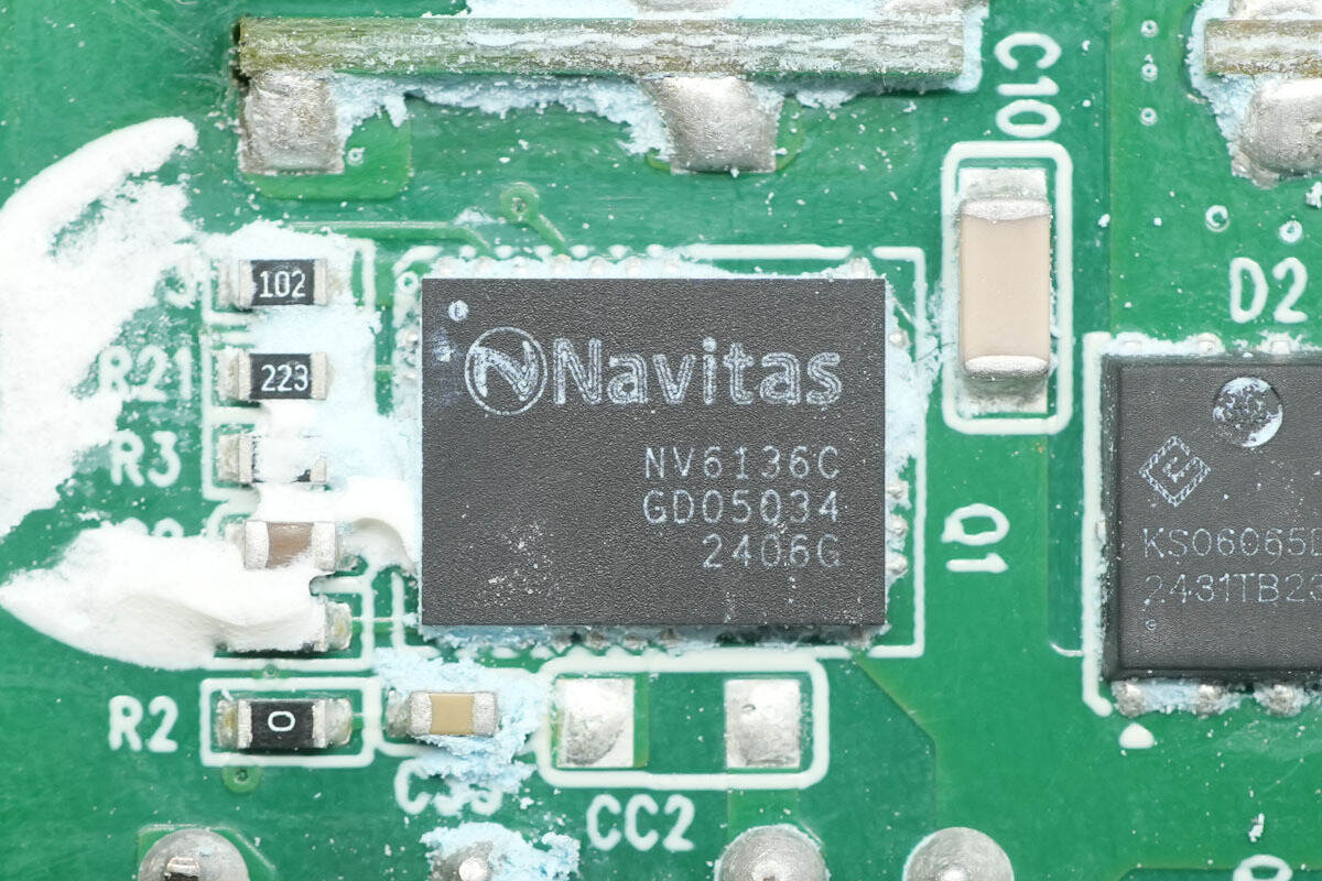
The master control chip uses the Navitas GaNSense Control integrated GaN chip NV9580. It features a built-in 170mΩ GaN FET and a high-frequency QR controller, offering lossless current detection, high integration, and high conversion efficiency, enabling compact fast-charging designs. It supports CCM/QR/DCM control modes and integrates protection features such as cycle-by-cycle current limiting, AOCP, OTP, and LPS, with ultra-low standby power consumption of only 20mW.
The NV9580 comes in a QFN 5x6 package, with a maximum switching frequency of 225kHz, allowing engineers to design flexibly, optimizing transformer size and EMI performance. The NV9580 does not require additional clamping circuits for a wide VDD range power supply, helping to save BOM costs and reduce PCB size.
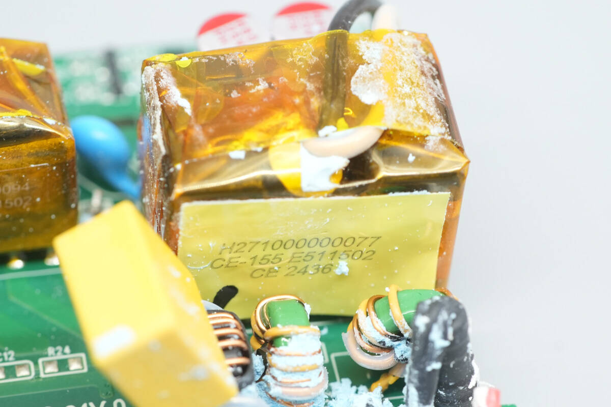
A close-up of the transformer.
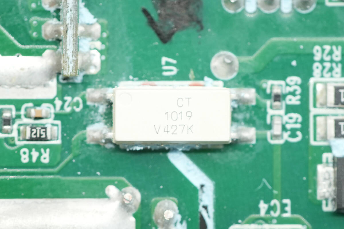
The CT1019 optocoupler is used for output voltage feedback.
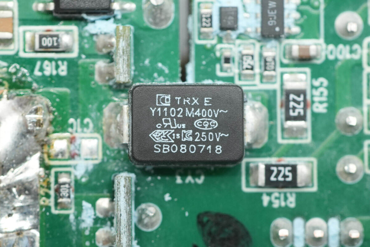
The SMD Y capacitor is from TRX. Its compact size and light weight make it ideal for high-density power products such as GaN fast chargers. The part number is TMY1102M.
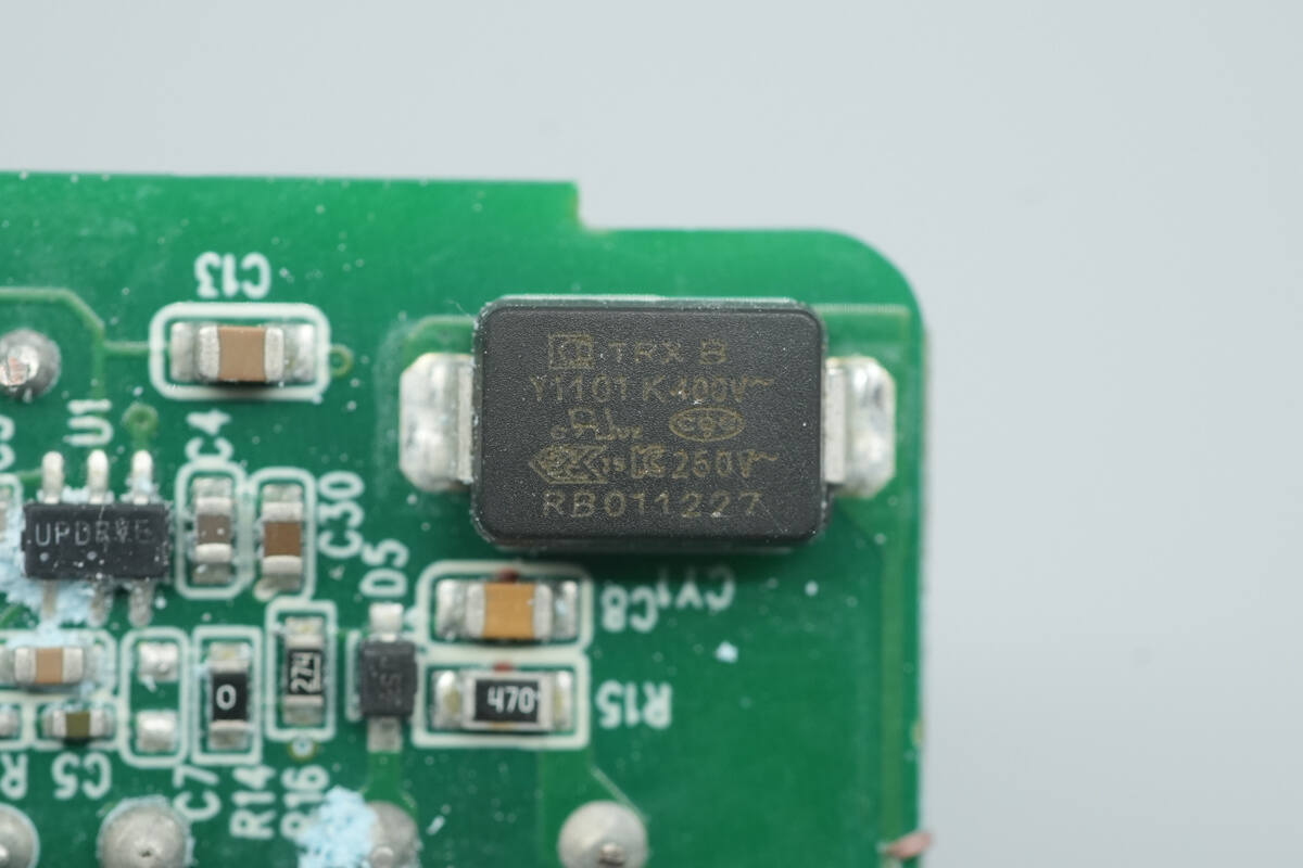
The other SMD Y capacitor has the part number TMY1101K.
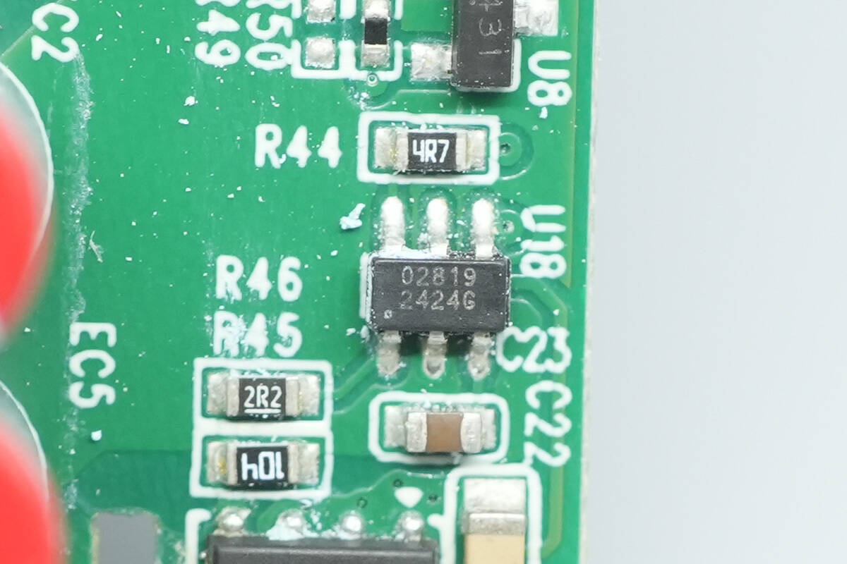
The synchronous rectifier controller is marked with 02819.
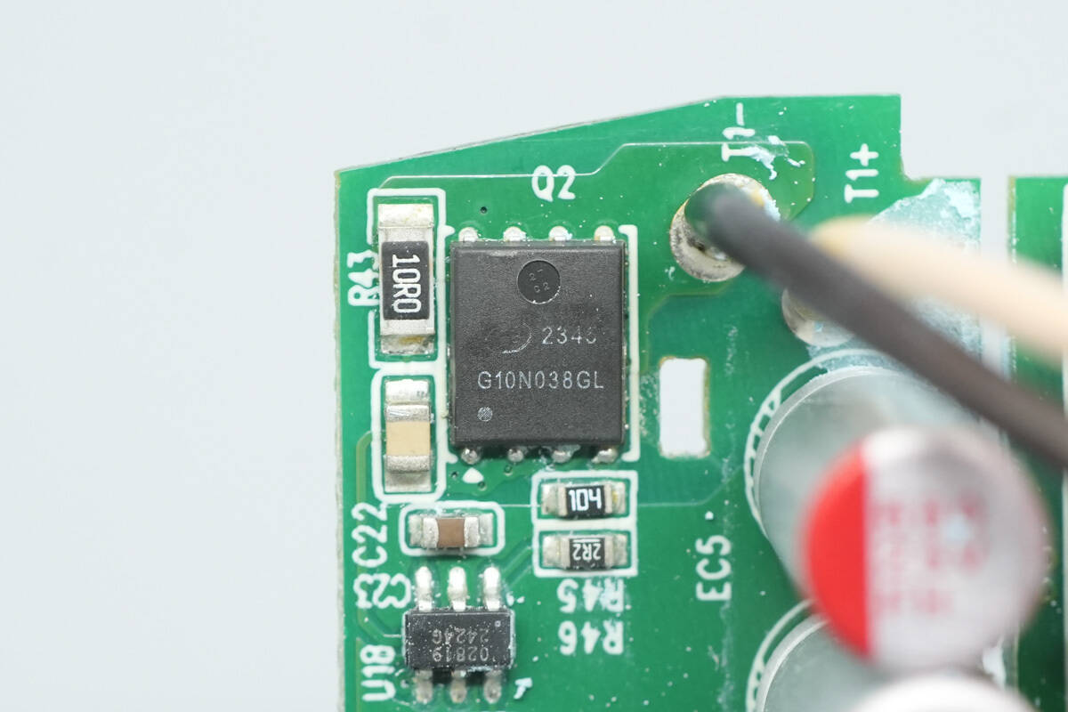
The synchronous rectifier is from ALKAIDSEMI, model AKG10N038GL. It is an NMOS with a voltage rating of 100V, a Rds(on) of 3.8mΩ, and comes in a PDFN 5x6 package.
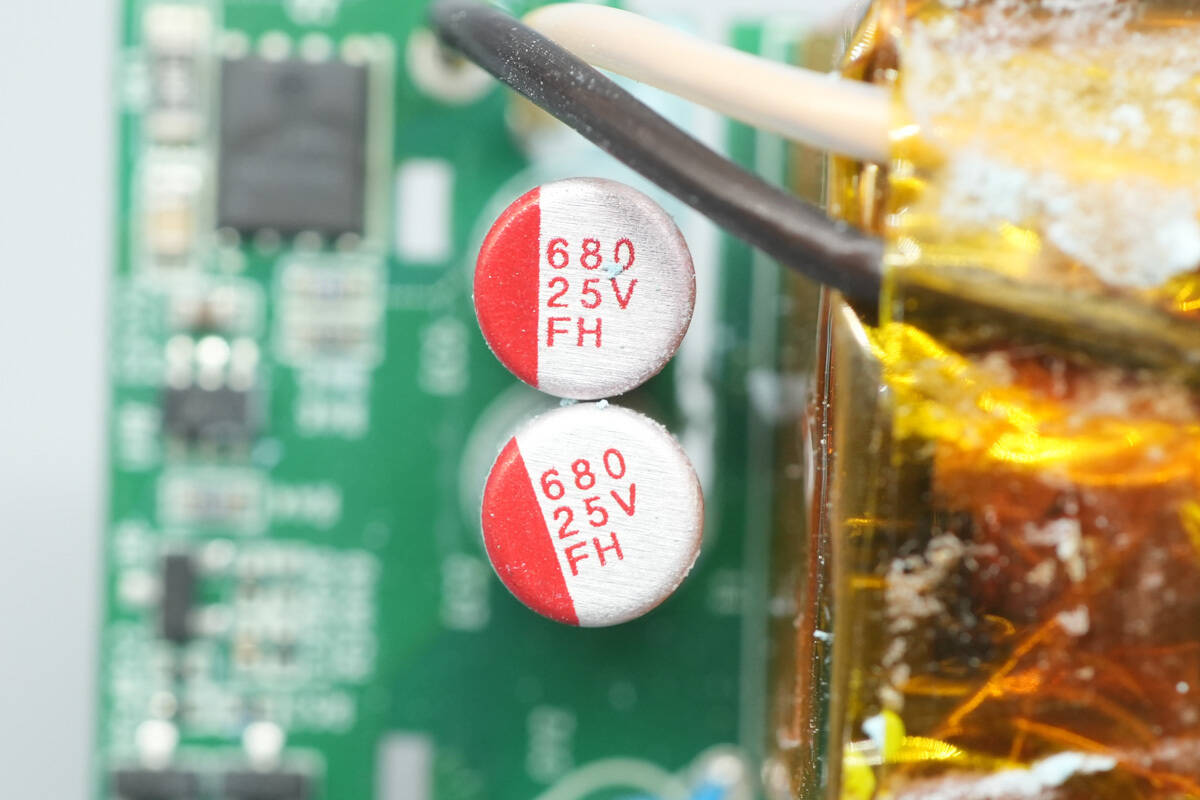
The two output filter solid capacitors have a specification of 25V, 680µF.
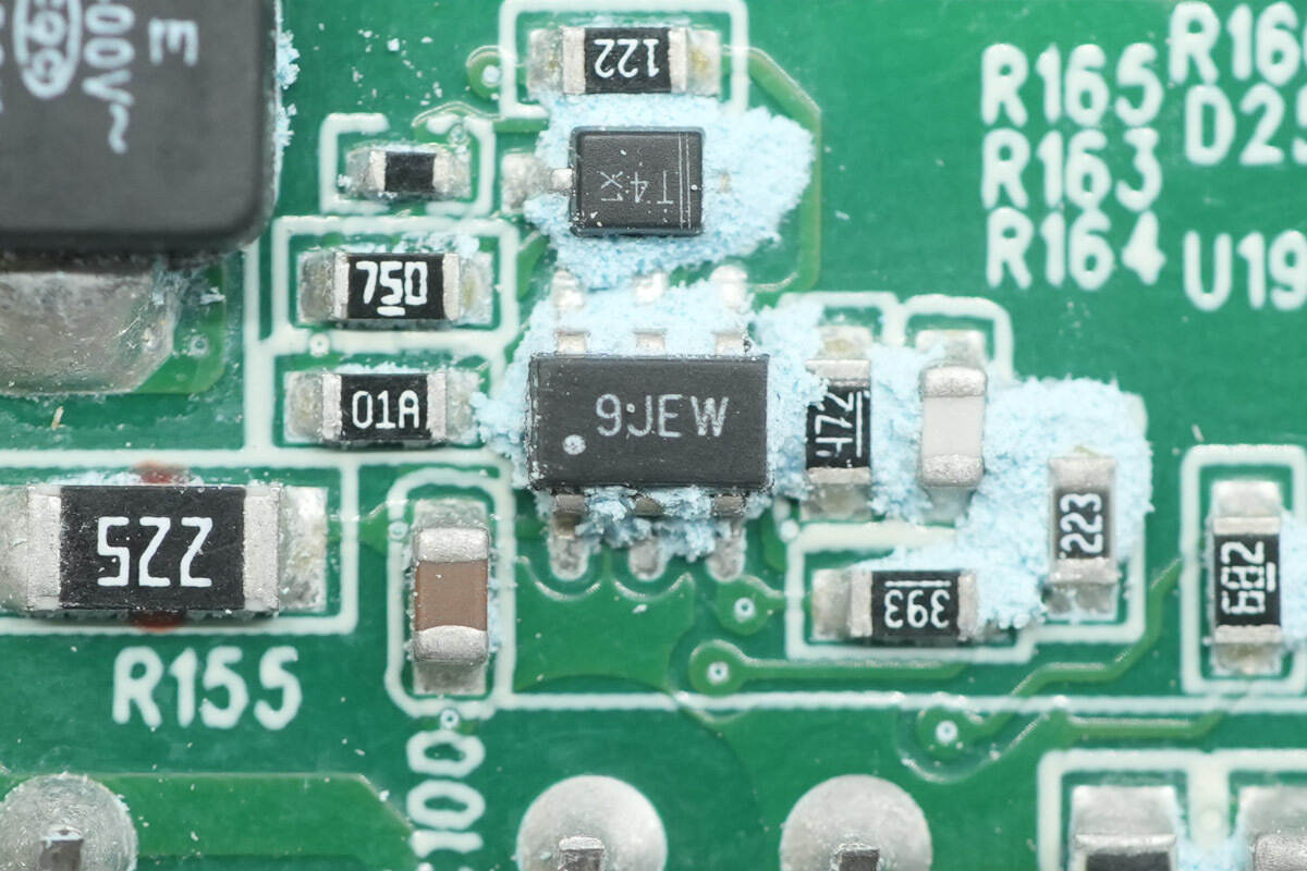
The primary controller of the other switch-mode power supply is marked with 9JEW.
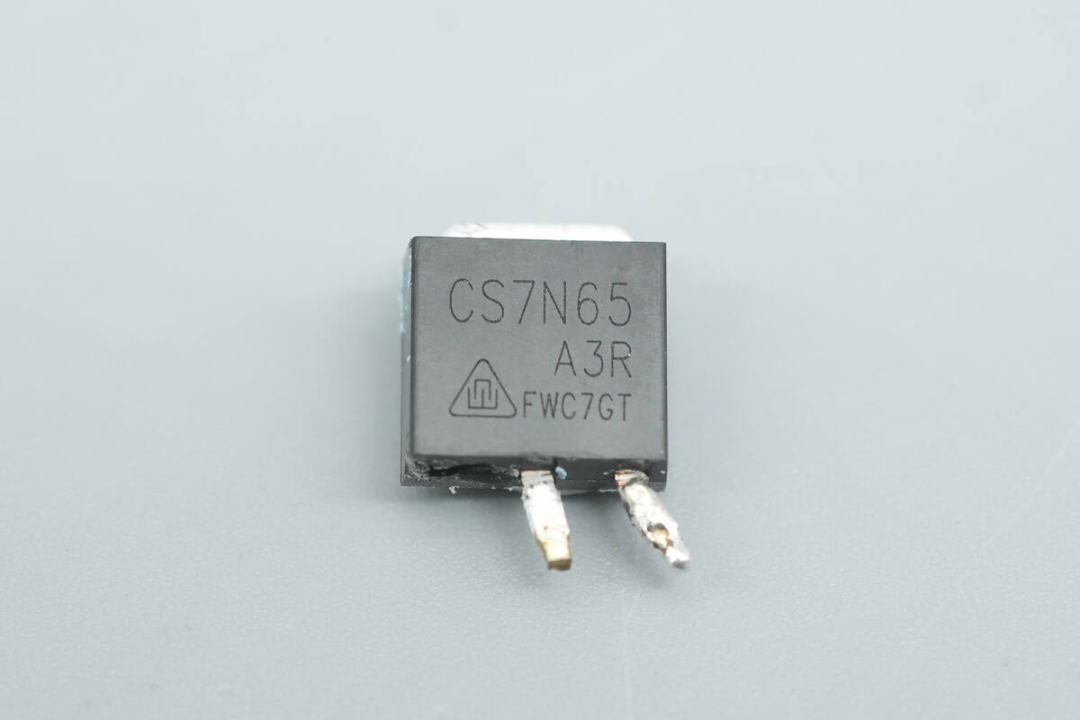
The primary MOSFET is from CR MICRO, model CS7N65A3R. It is an NMOS with a voltage rating of 650V, an Rds(on) of 1.2Ω, and comes in a TO251 package.
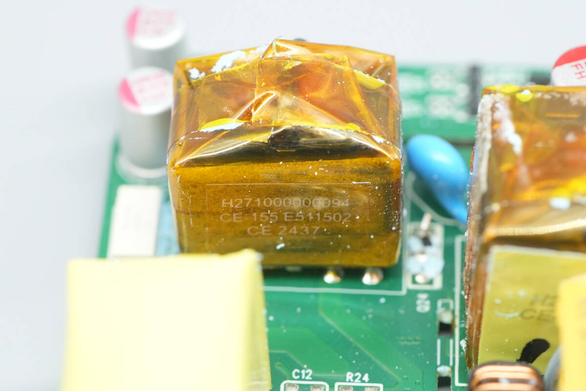
A close-up of the transformer.
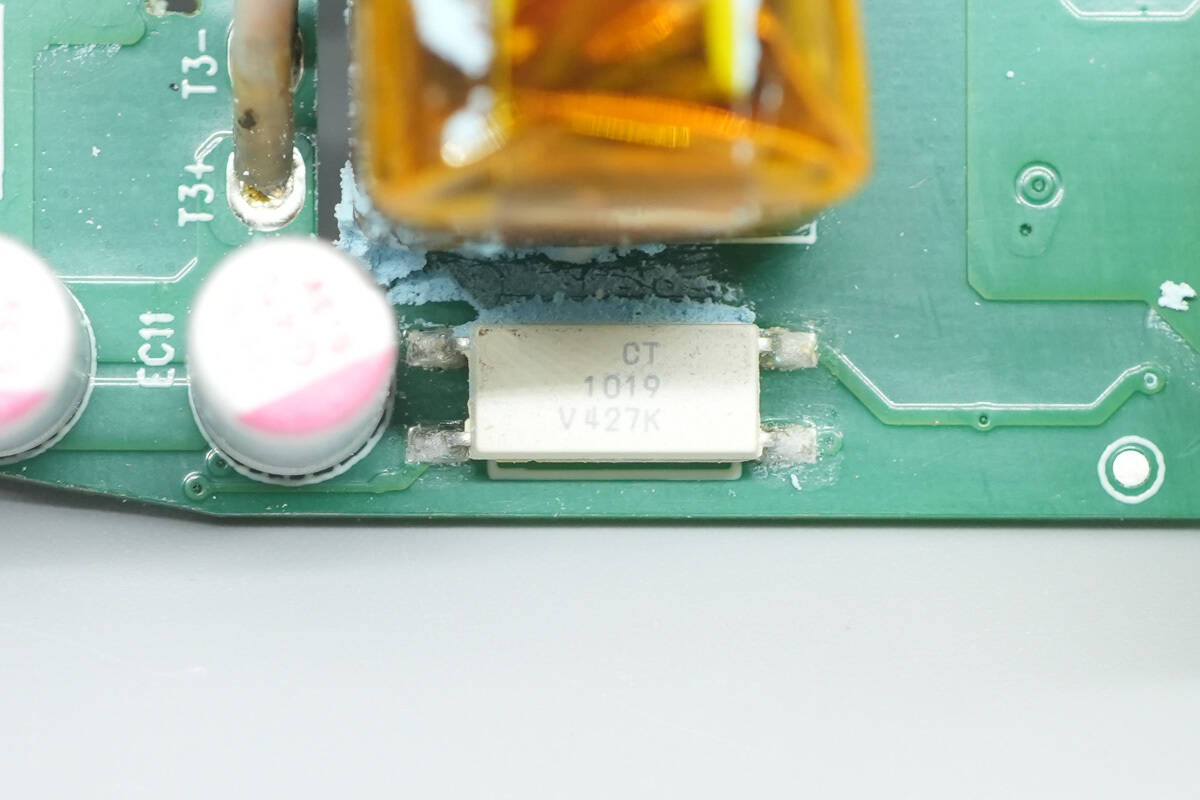
The CT1019 optocoupler is used for output voltage feedback.
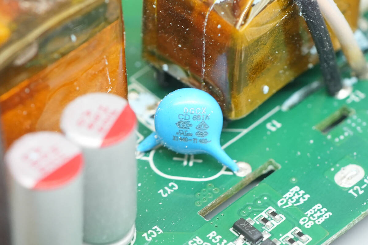
The blue Y capacitor is from DGCX.
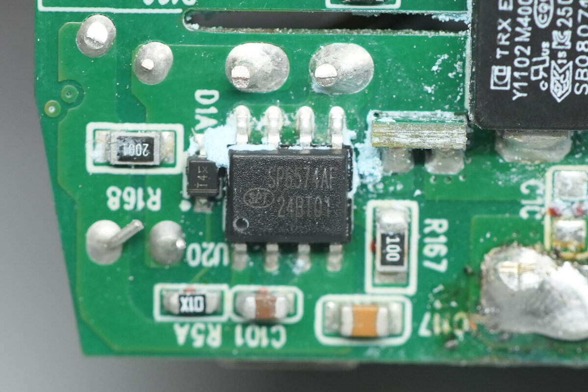
The synchronous rectifier chip used for the 5V output of the USB-A port is from Si-power, model SP6574AF. This is a high-performance switch-mode power supply secondary-side synchronous rectifier controller. It easily meets Level 6 energy efficiency in low-voltage, high-current switch-mode power supply applications, making it an ideal solution for ultra-low conduction voltage drop rectifiers.
The chip features a built-in NMOSFET synchronous rectifier with a voltage rating of 45V and ultra-low internal resistance, enabling it to deliver low-voltage, high-current application outputs. It also integrates high-voltage direct detection technology, with a voltage rating of up to 120V. It supports switching frequencies up to 300KHz and is compatible with CCM/QR/DCM switch-mode power supply operation modes. The chip's extremely low conduction losses are much lower than those of Schottky diodes, significantly improving the system's conversion efficiency and greatly reducing the rectifier components' temperature.
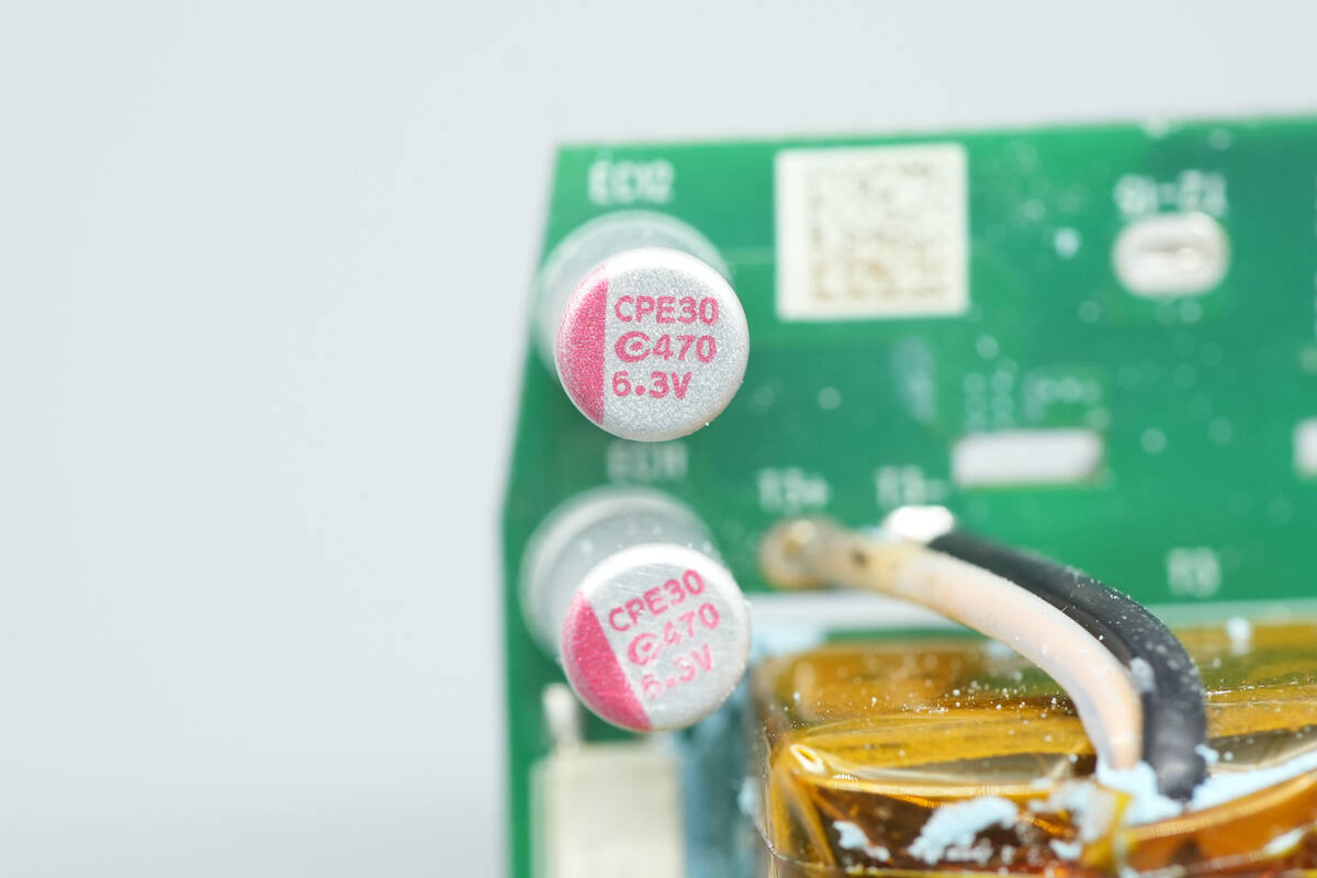
The two output filter solid capacitors are from APAQ, with a specification of 6.3V, 470µF.
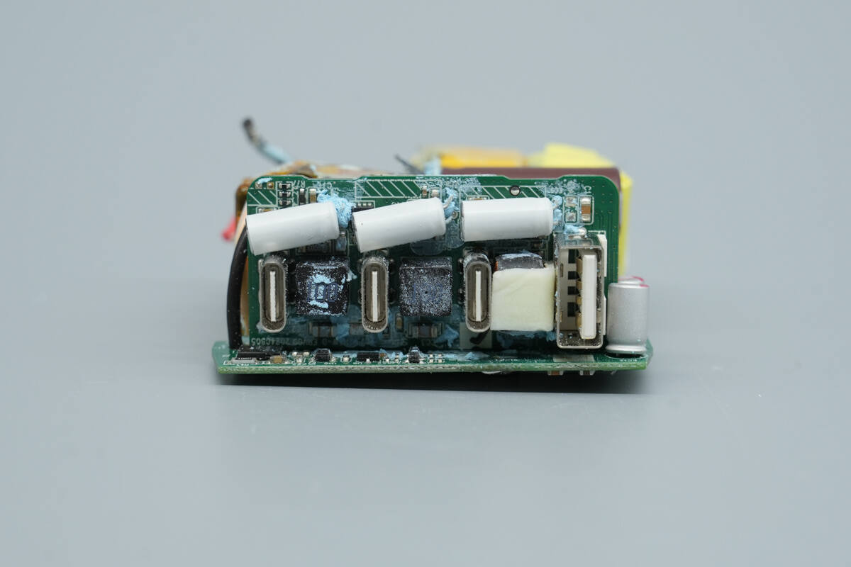
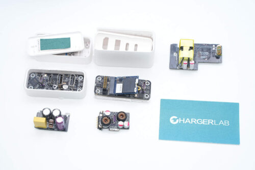
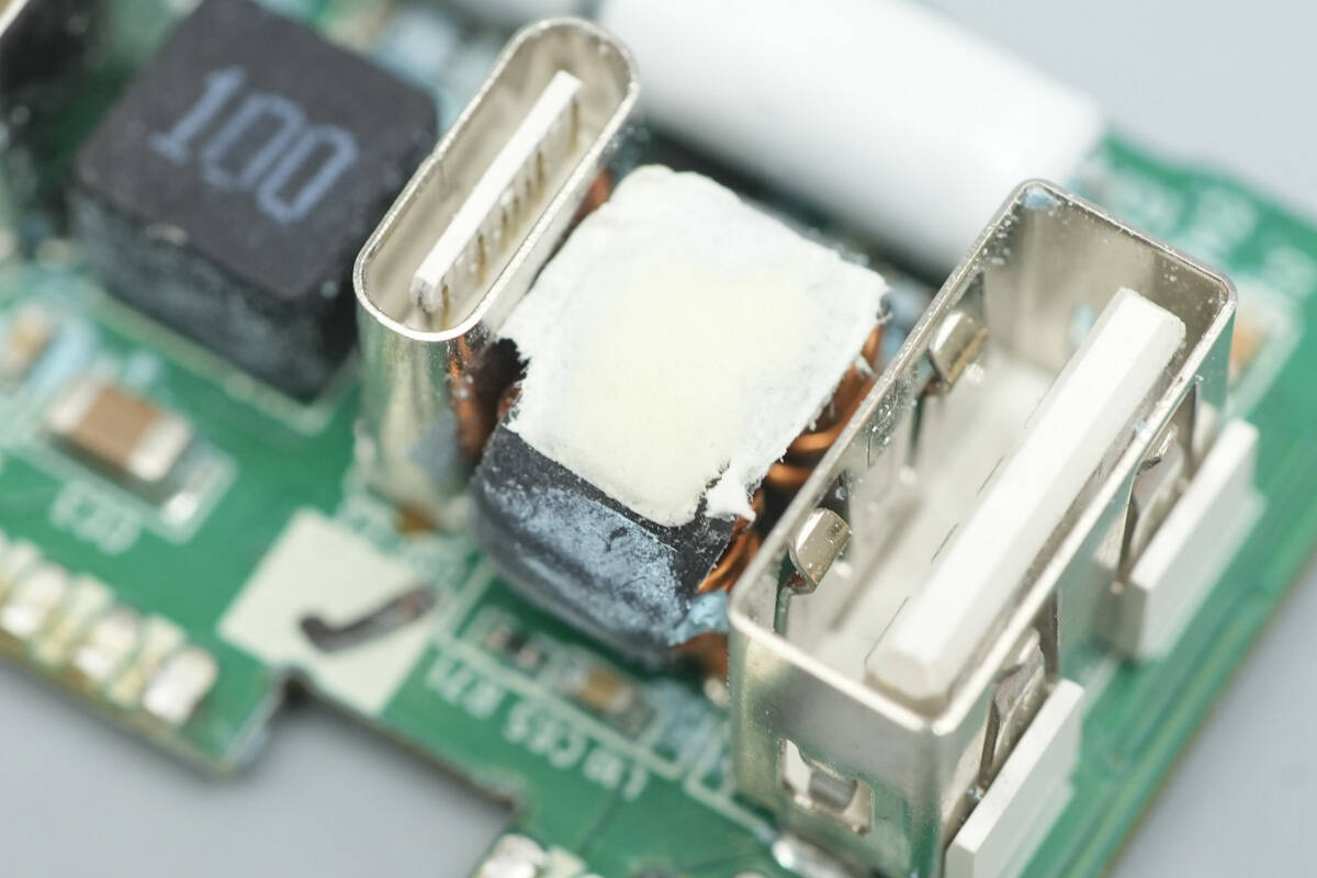
The four interface sockets are located on the small PCB.
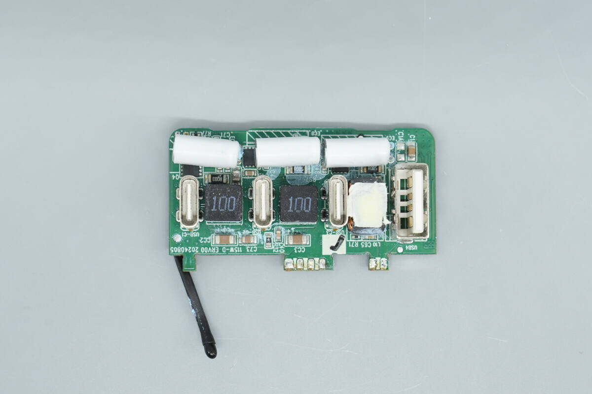
After removing the small PCB, the front side features three step-down inductors for the secondary buck circuits, solid capacitors, and VBUS MOSFETs.
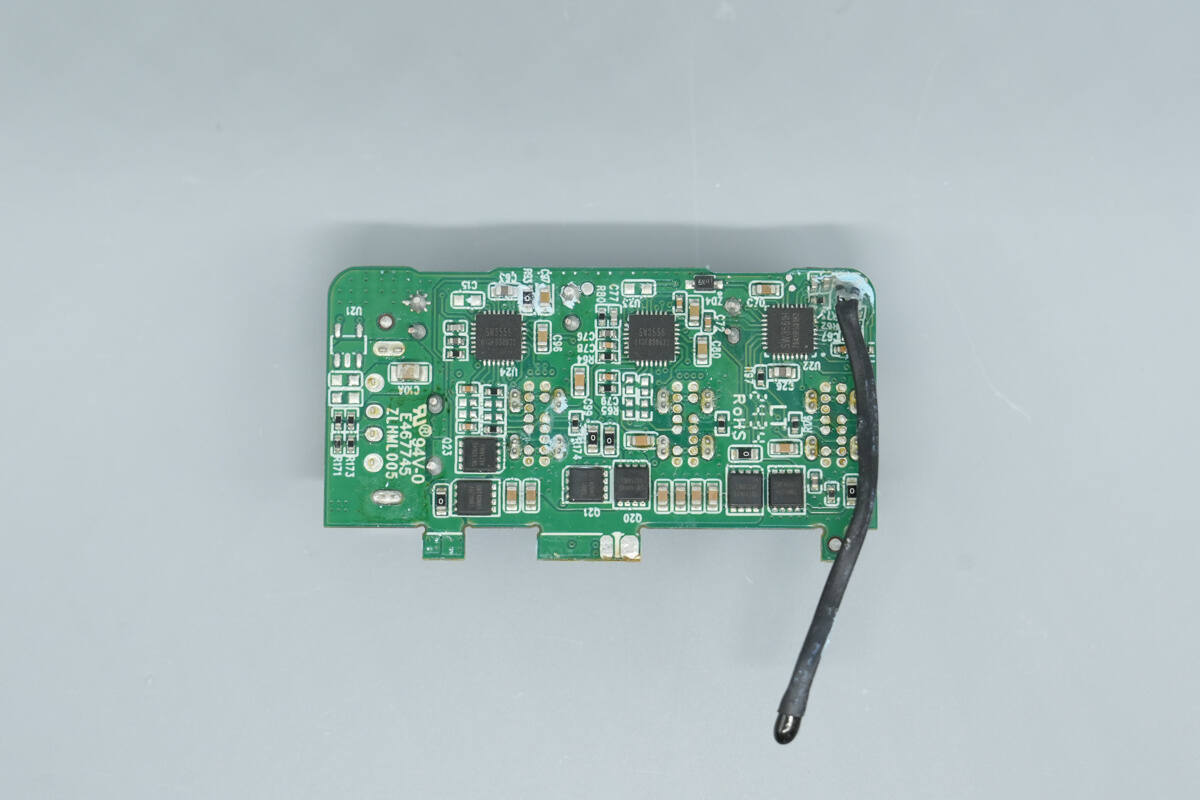
The backside features buck protocol chips, synchronous buck MOSFETs, and a thermistor.
A close-up of the thermistor.
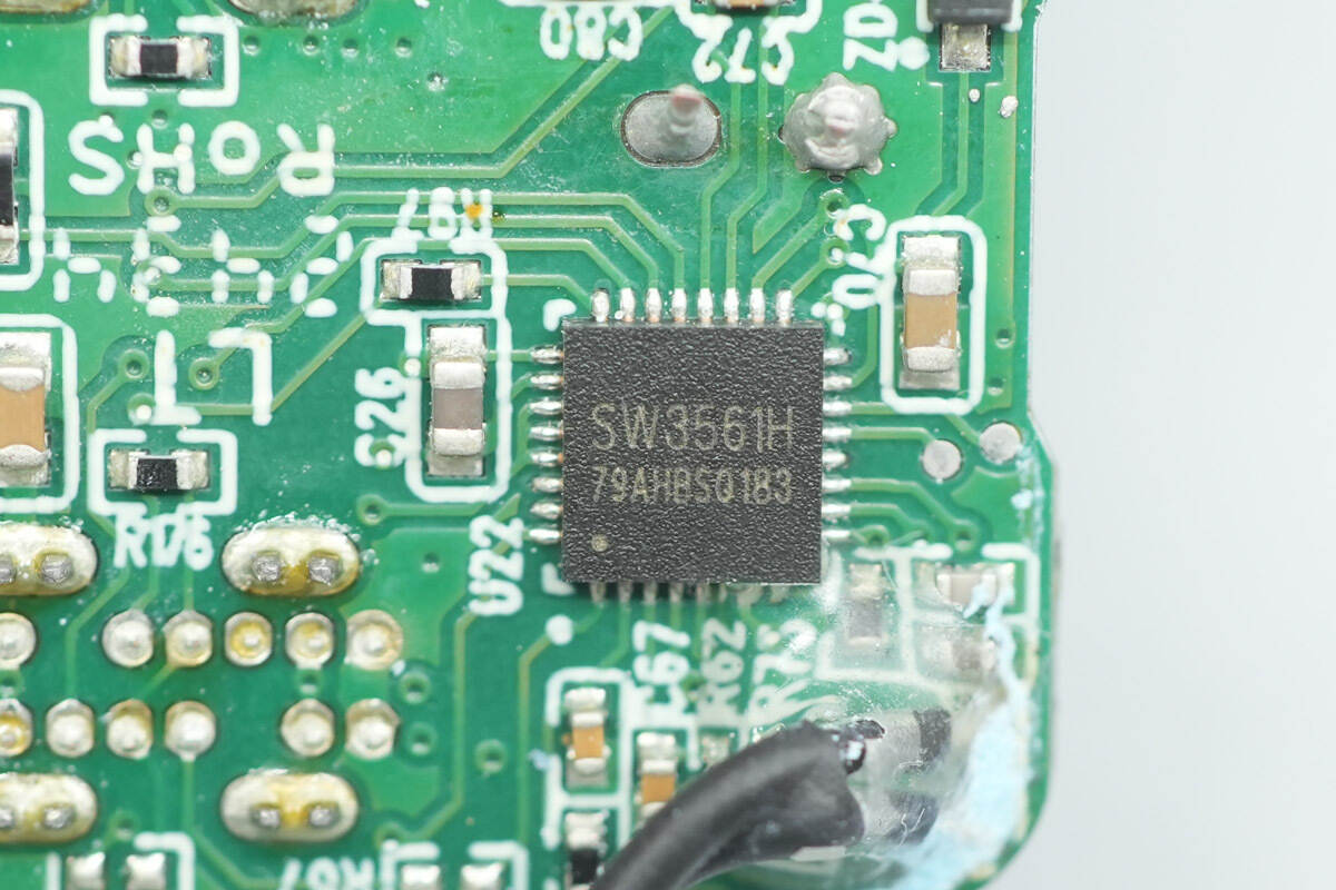
The buck protocol chip for the USB-C1 port is the iSmartWare SW3561H. This is a buck SoC chip that supports dual USB-C output ports. It integrates a high-efficiency synchronous buck controller and supports a 20V 5A power output, along with USB PD 3.1 SPR. The chip includes an ARM Cortex-M0 core, integrated Type-C logic, and supports fast charging protocols such as PD 3.1, QC, SCP, and UFCS, with the ability to customize fast charging protocols.
The iSmartWare SW3561H supports dual USB-C port control, with wire loss compensation. Paired with two synchronous buck MOSFETs and the corresponding VBUS MOSFETs for each port, it enables dual-port buck output. The built-in buck converter operates at a default frequency of 180KHz, with customizable working frequencies, and supports up to 100W of power output, making it suitable for compact designs. The chip integrates comprehensive protection features, including overheat protection, input/output overvoltage/undervoltage protection, output overcurrent protection, and data pin overvoltage protection. It comes in a QFN-32 package.
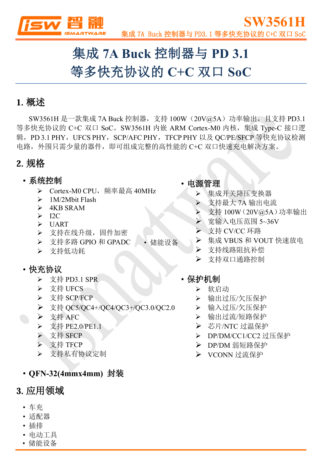
Here is the information about iSmartWare SW3561H.
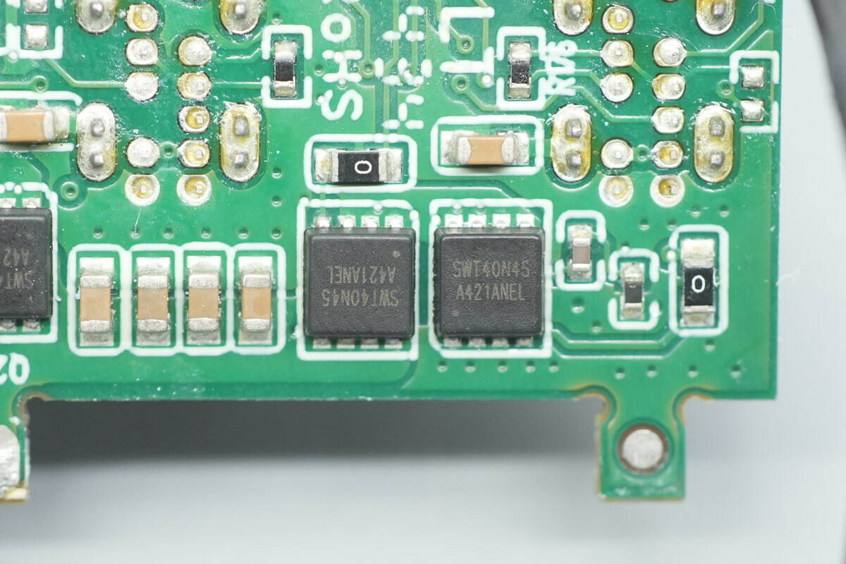
The two synchronous buck MOSFETs are from iSmartWare, model SWT40N45, and they come in a PDFN3030 package.
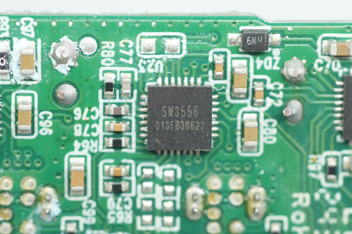
The USB-C2 port buck output uses the iSmartWare SW3556, which supports dual USB-C port buck control. It integrates multiple fast-charging protocols, supports up to 7A high-current output, and enables dual-port power-blind insertion and independent current limiting. The SW3556 supports driving low-voltage GaN FETs, which further improves the efficiency of the buck converter, reduces the size of the charger, and lowers heat dissipation requirements.
The SW3556 is a synchronous rectification buck topology that supports 40V input. It integrates a synchronous rectification buck controller, and when paired with silicon MOSFETs or GaN FETs, inductors, capacitors, and other simple external components, it can achieve a high power output of up to 140W. The built-in buck controller operates at a switching frequency of 125KHz and supports both PFM and PWM modes to optimize conversion efficiency.
Additionally, the SW3556 supports external resistors on its pins to configure output power and dynamic power distribution, eliminating the need for an external microcontroller when developing multi-port fast charging power products. This enables a more streamlined design and reduces costs. It is suitable for applications such as in-vehicle chargers, multi-port chargers, power strips, and other similar products.
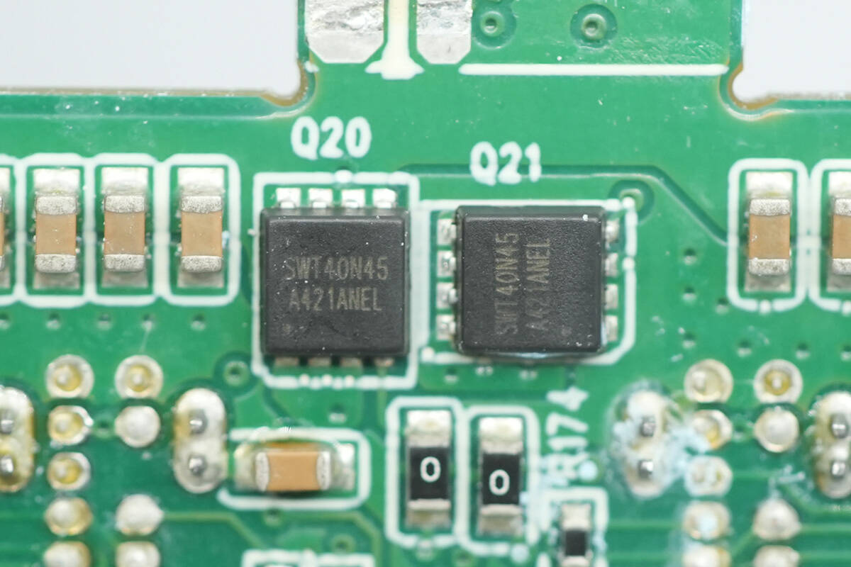
The two synchronous buck MOSFETs are from iSmartWare, model SWT40N45.
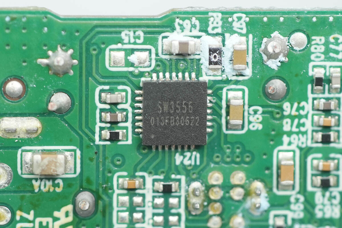
The buck protocol chip for the USB-C3 port also uses the iSmartWare SW3556.
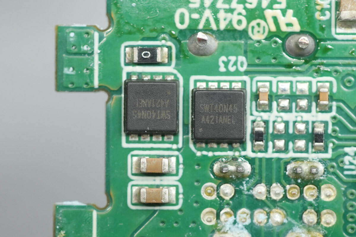
The two synchronous buck MOSFETs are also from iSmartWare, model SWT40N45.
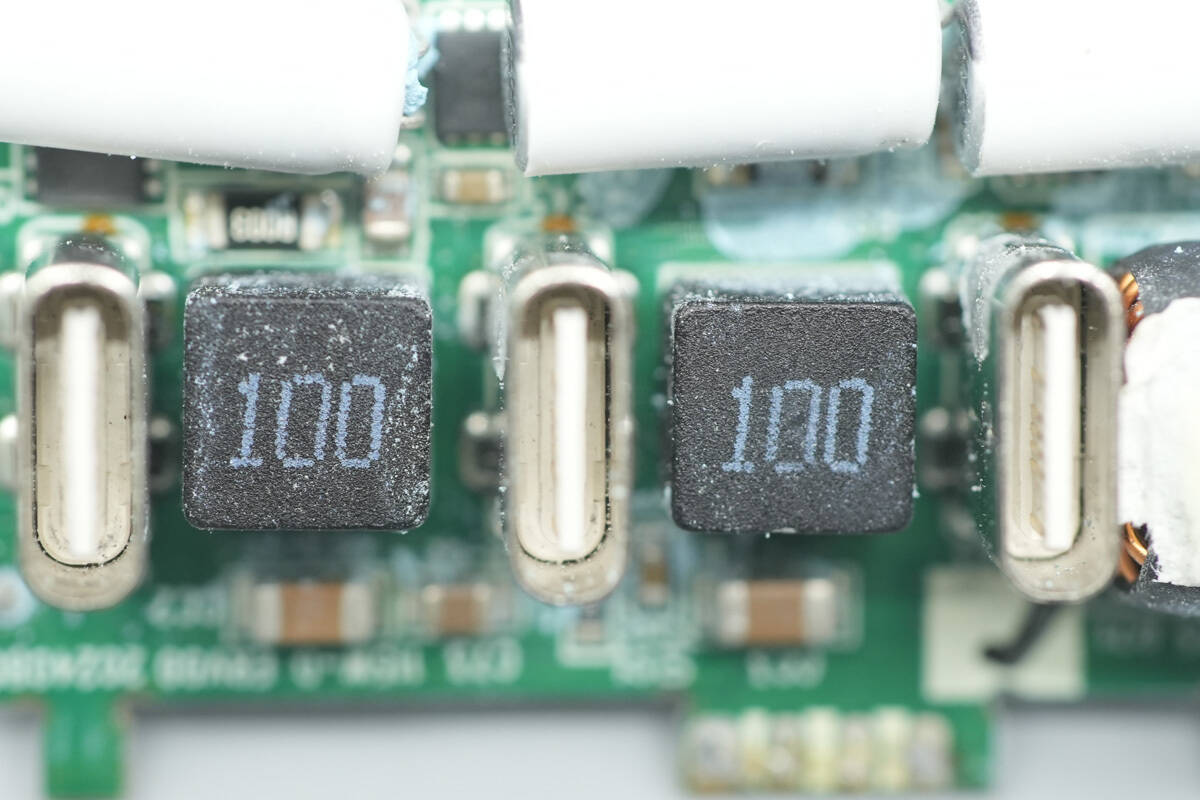
A close-up of the two buck inductors.
A close-up of the third buck inductor.
The solid capacitors for the three secondary buck circuits all have the same specification of 25V, 220µF.
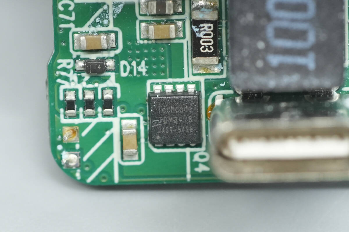
The VBUS MOSFET for the USB-C1 port is from Techcode, model TDM3478. It is an NMOS with a voltage rating of 30V, an Rds(on) of 5mΩ, and comes in a PPAK-3*3-8 package.
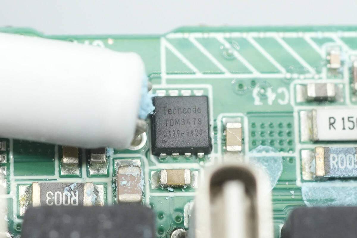
The VBUS MOSFET for the USB-C2 port also uses the Techcode TDM3478.
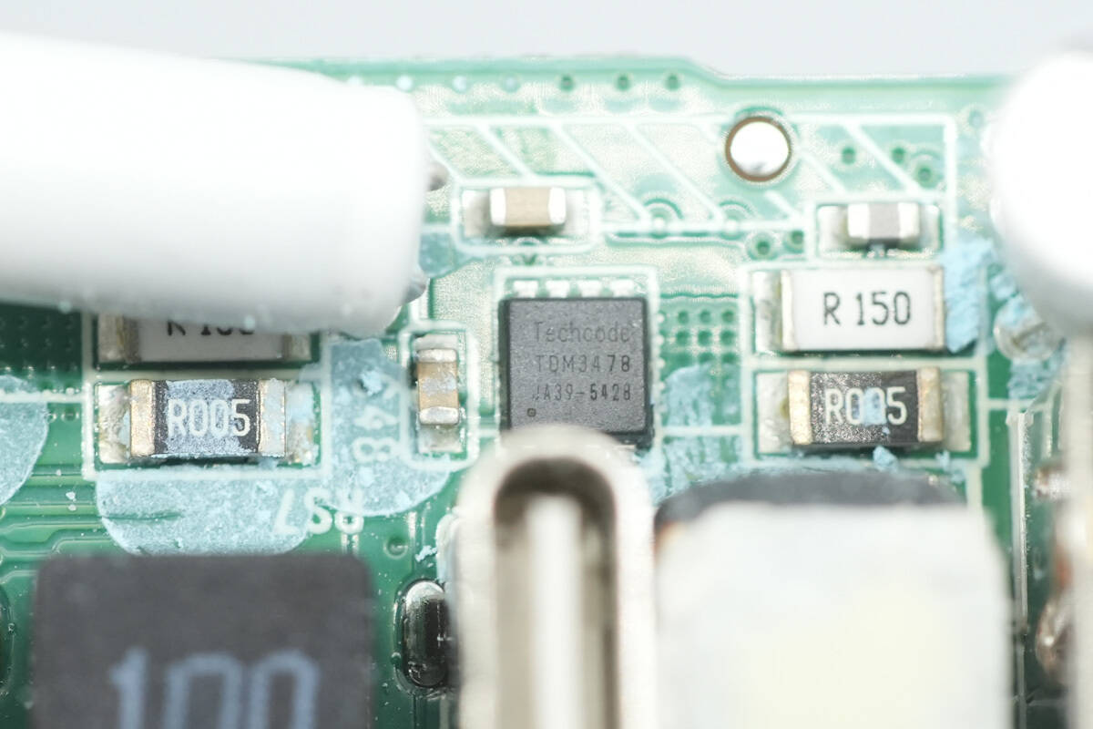
The VBUS MOSFET for the USB-C3 port also uses the Techcode TDM3478.

Well, those are all components of the Belkin 112W 4-Port GaN Charger.
Summary of ChargerLAB
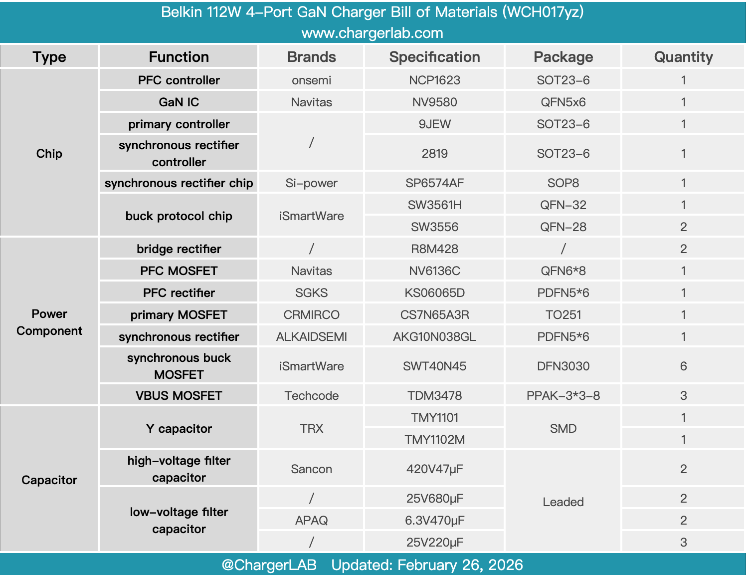
Here is the component list of the Belkin 112W 4-Port GaN Charger for your convenience.
The shell is made of recycled plastic with a matte finish. It features foldable prongs for easy storage and portability. The charger is equipped with 3 USB-C ports and 1 USB-A port. All three USB-C ports support 100W fast charging and are compatible with protocols such as PD3.0, PPS, and QC5, with a total maximum output of 112W.
After taking it apart, we found that the internal structure is compact, with multiple small PCBs soldered onto the PCBA module. The interior is filled with a large amount of thermal paste and thermal pads, and is covered with copper sheets and Mylar sheets. The PFC boost is achieved efficiently and stably using the Onsemi NCP1623 PFC controller, paired with the Navitas NV6136C GaN power chip and SGKS silicon carbide diode. The switch-mode power supply for the three USB-C ports uses the Navitas NV9580 integrated GaN chip, while the output is controlled by the iSmartWare SW3561H and SW3556 buck protocol chips, supporting multiple fast charging protocols and enabling intelligent power distribution.
Related Articles:
1. Teardown of Meizu PANDAER 66W Vertical Air-cooled Wireless Charger (WP06)
2. Teardown of VERTIV 3500W SiC Rectifier Module (R48-3500e3)
3. Teardown of EcoFlow 240W USB4 Fast Charging Braided Cable