Introduction
Recently, we got our hands on the Baseus 65W GaN5 Pro charger. It features a compact design with foldable prongs, making it highly portable. It is equipped with two USB-C ports and one USB-A port. Both USB-C ports support 65W output and offer automatic power distribution. The USB-A port supports up to 60W output as well. Now, let’s take a closer look at the internal design and components.
Product Appearance
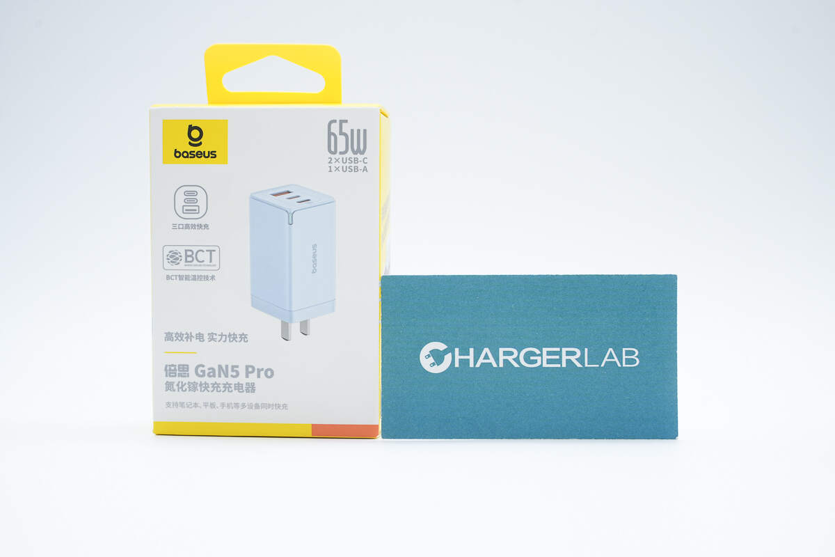
The front of the packaging shows the Baseus logo, product name, image of the charger, and its key selling points.
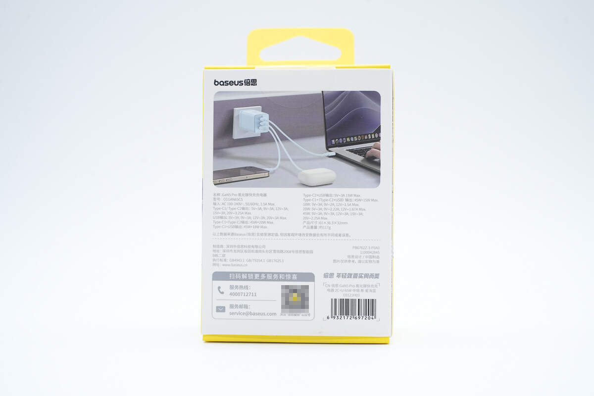
The back of the packaging displays the usage scenario and specification information.
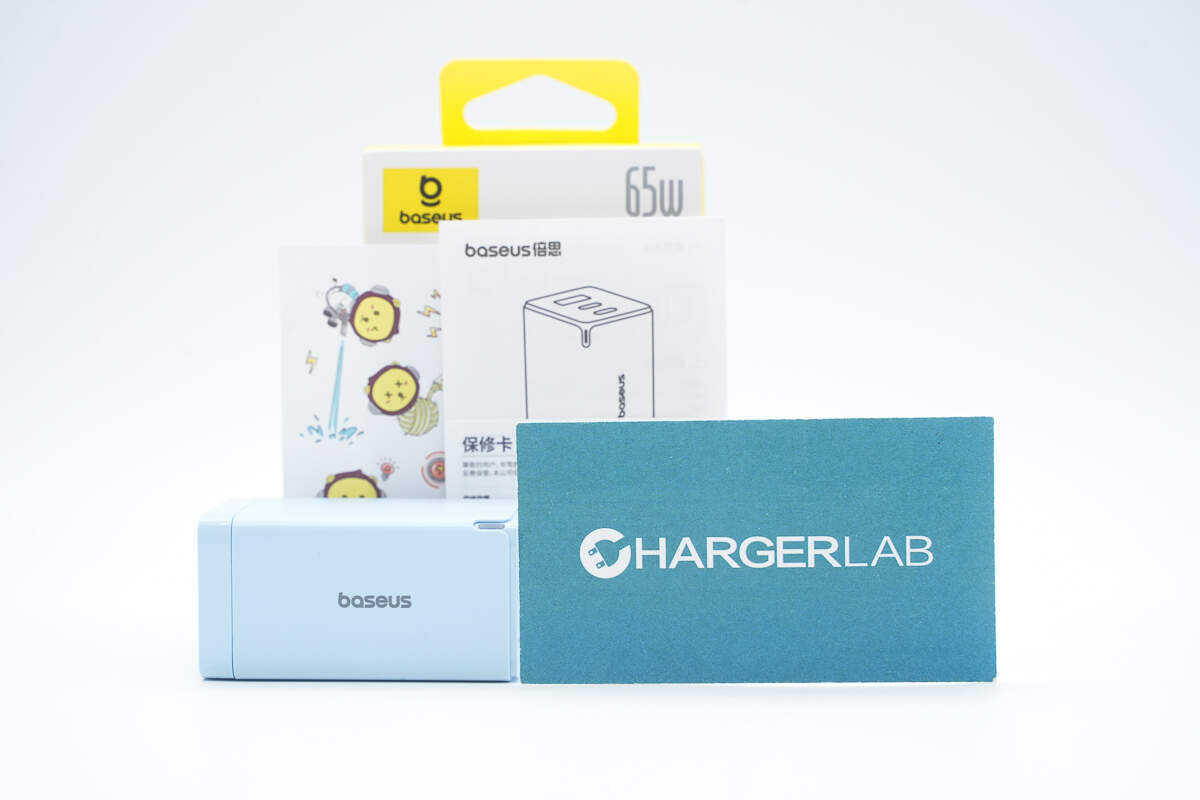
The package includes the charger and some documents.
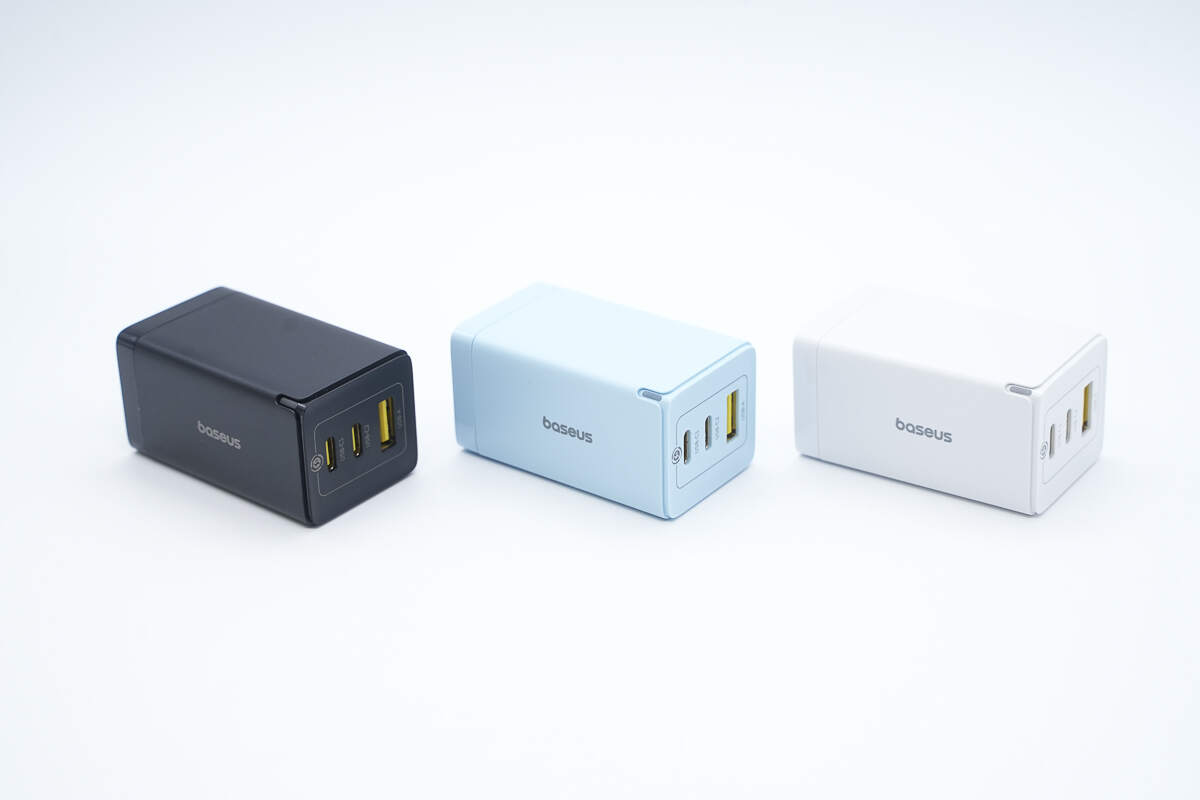
It is available in three color options: black, white, and blue.
The casing is made of fire-resistant PC material with a matte finish.
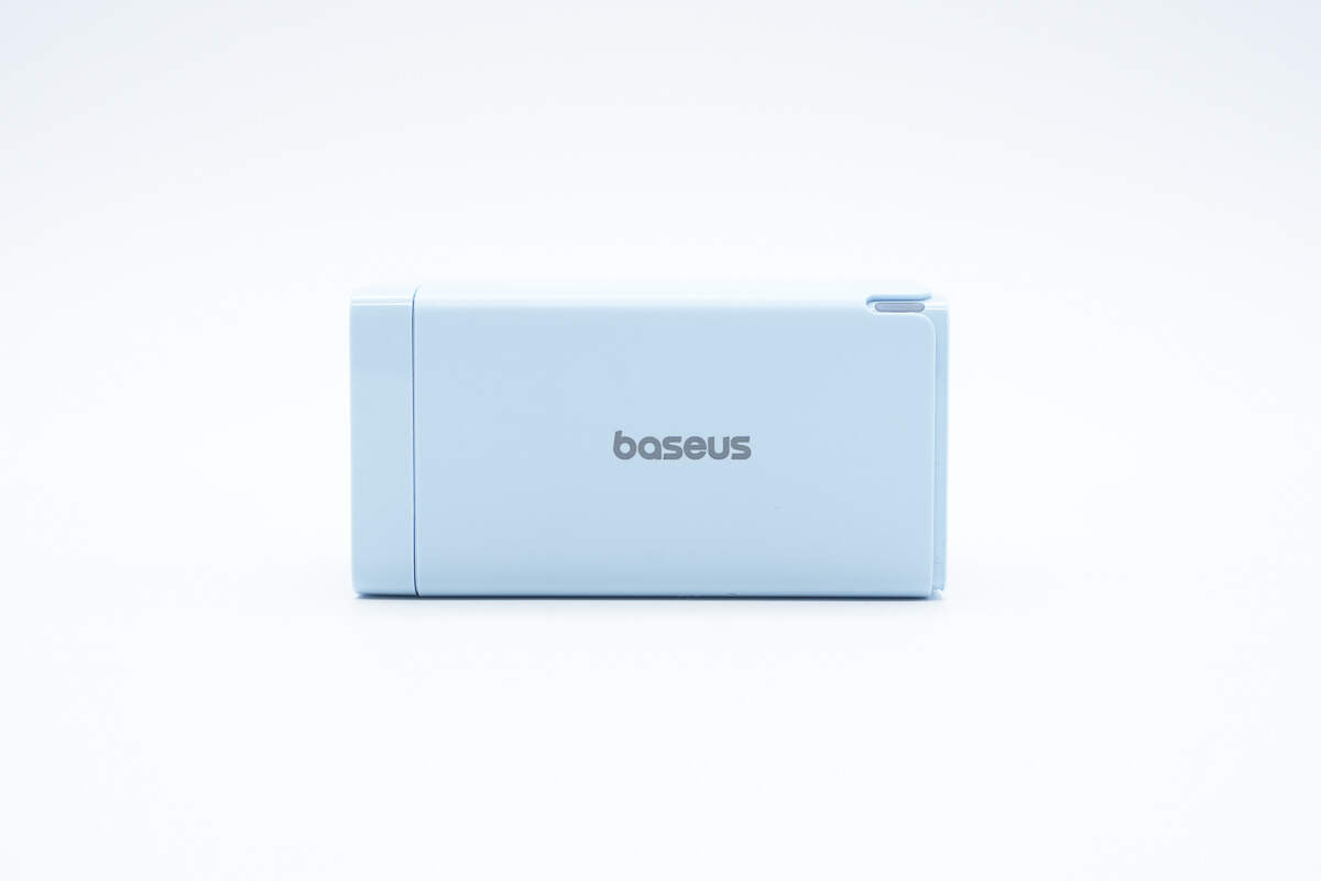
This side features the Baseus logo.
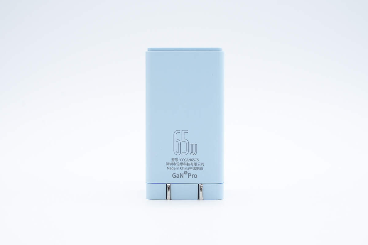
The back is printed with the model number CCGAN65C5, 65W, and GaN5 Pro.
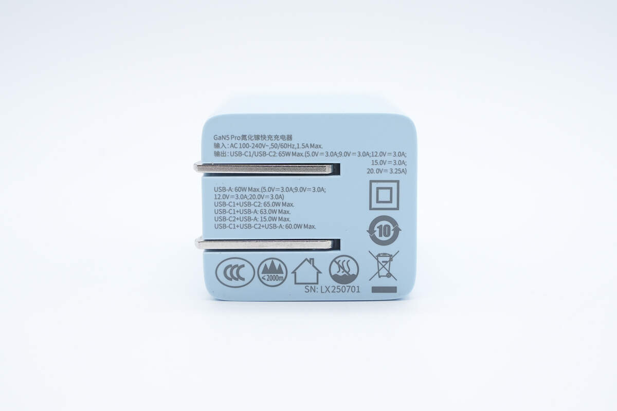
The input end is printed with the spec info.
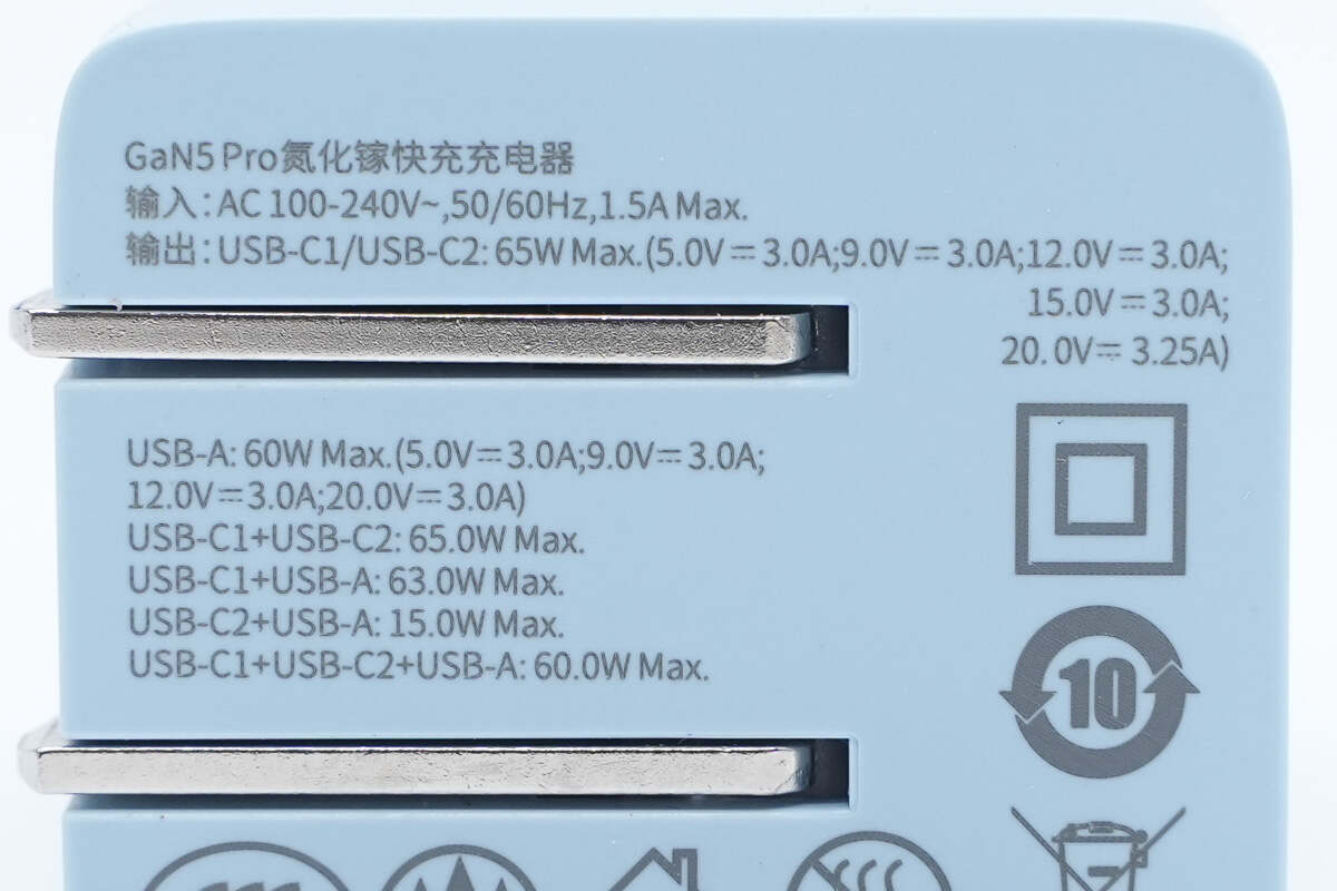
Input: AC 100-240V\~50/60Hz 1.5A Max
USB-C1/C2 Output: 5V3A, 9V3A, 12V3A, 15V3A, 20V3.25A (65W Max)
USB-A Output: 5V3A, 9V3A, 12V3A, 20V3A
USB-C1 + USB-C2: 65W
USB-C1 + USB-A: 63W
USB-C2 + USB-A: 15W
USB-C1 + USB-C2 + USB-A: 60W
Certified by ETL, FCC, and VI-level energy efficiency certification.
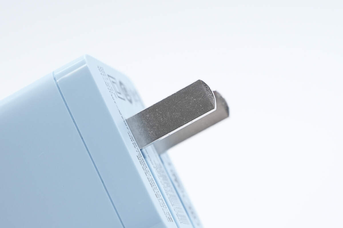
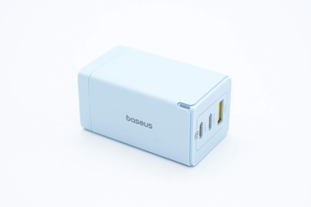
It is equipped with foldable prongs.
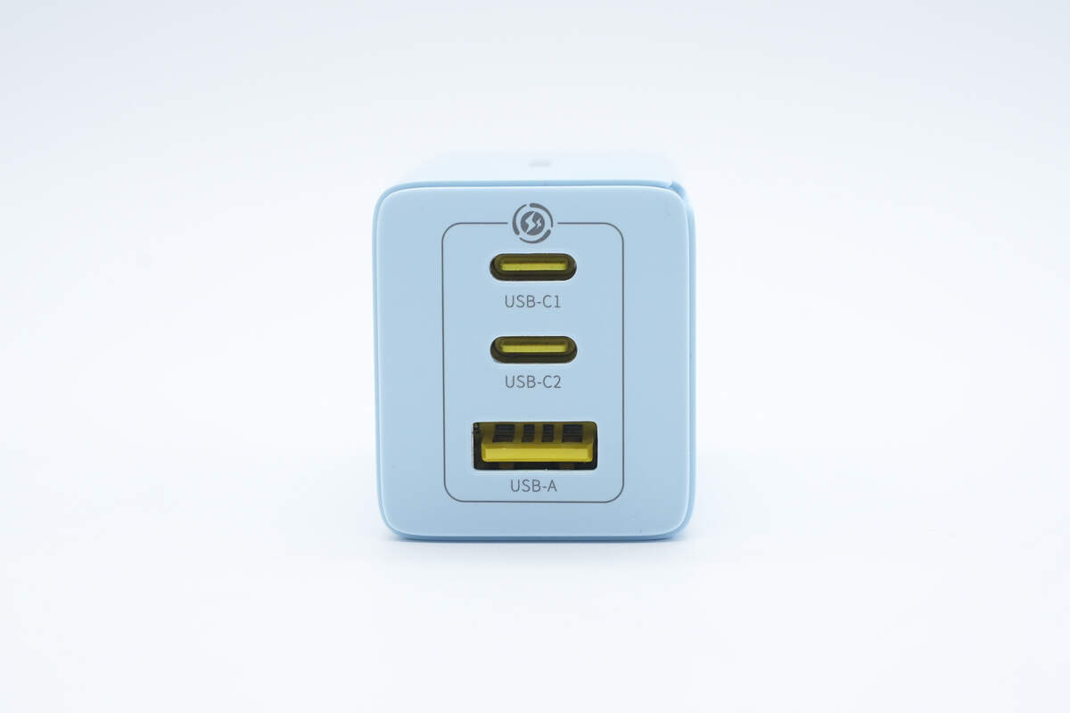
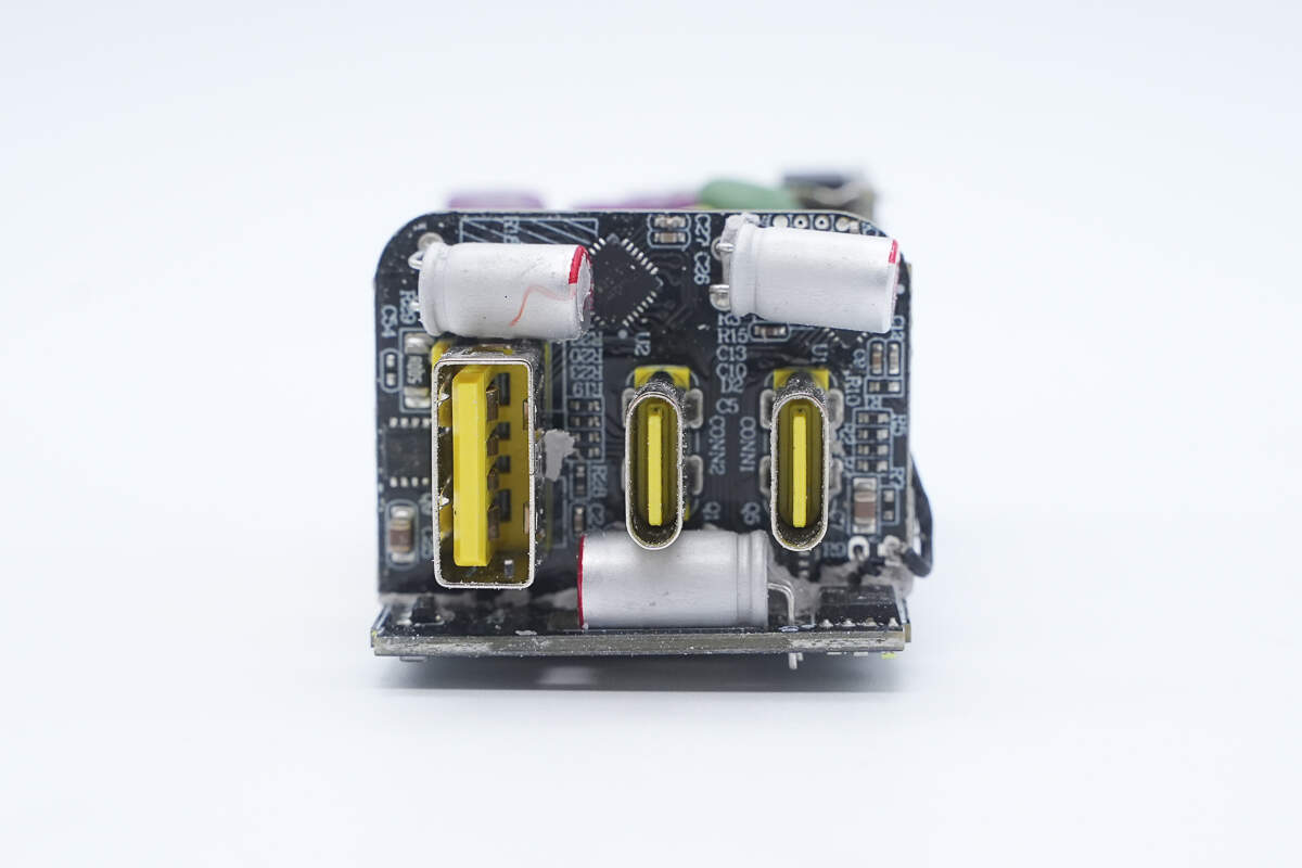
The output ports include two USB-C and one USB-A interfaces, and the plastic sheets are all yellow.
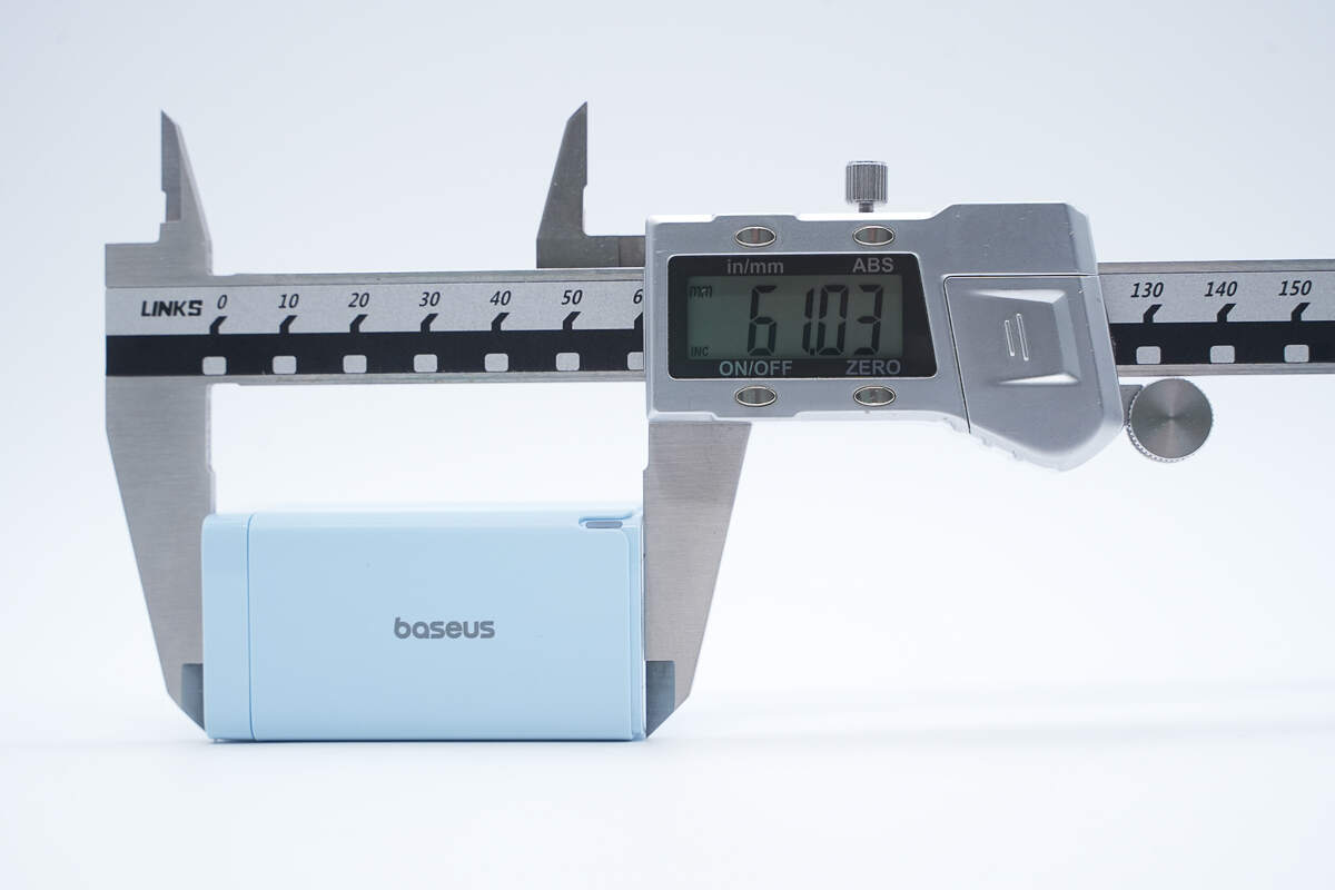
The length of the charger is about 61.03 mm (2.4 inches).
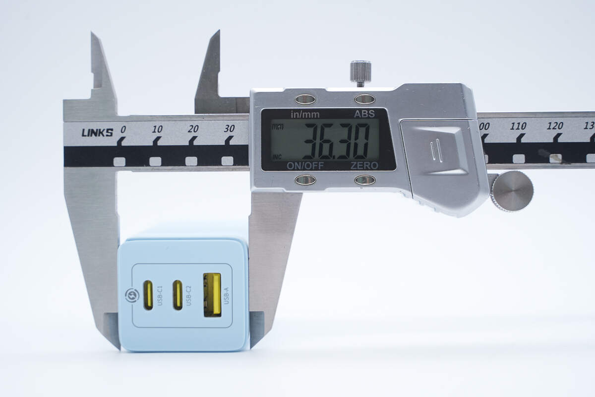
The width is about 36.3 mm (1.43 inches).
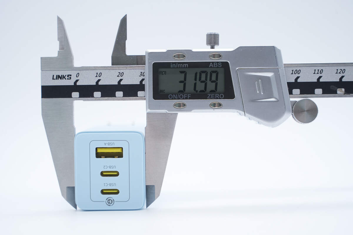
The thickness is about 31.99 mm (1.26 inches).
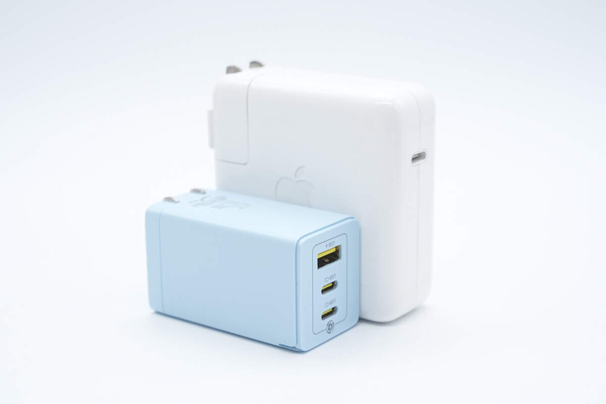
It is much smaller than the Apple 67W charger.
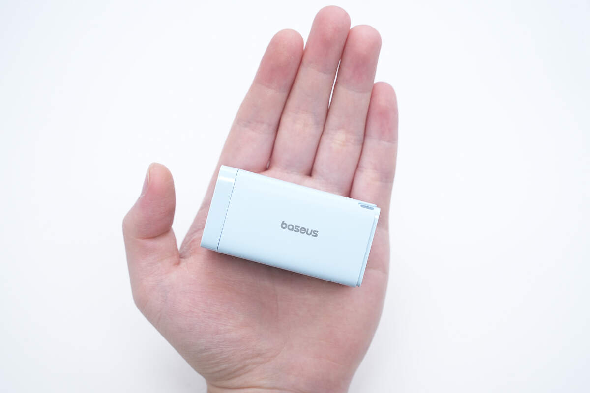
That's how big it is in the hand.
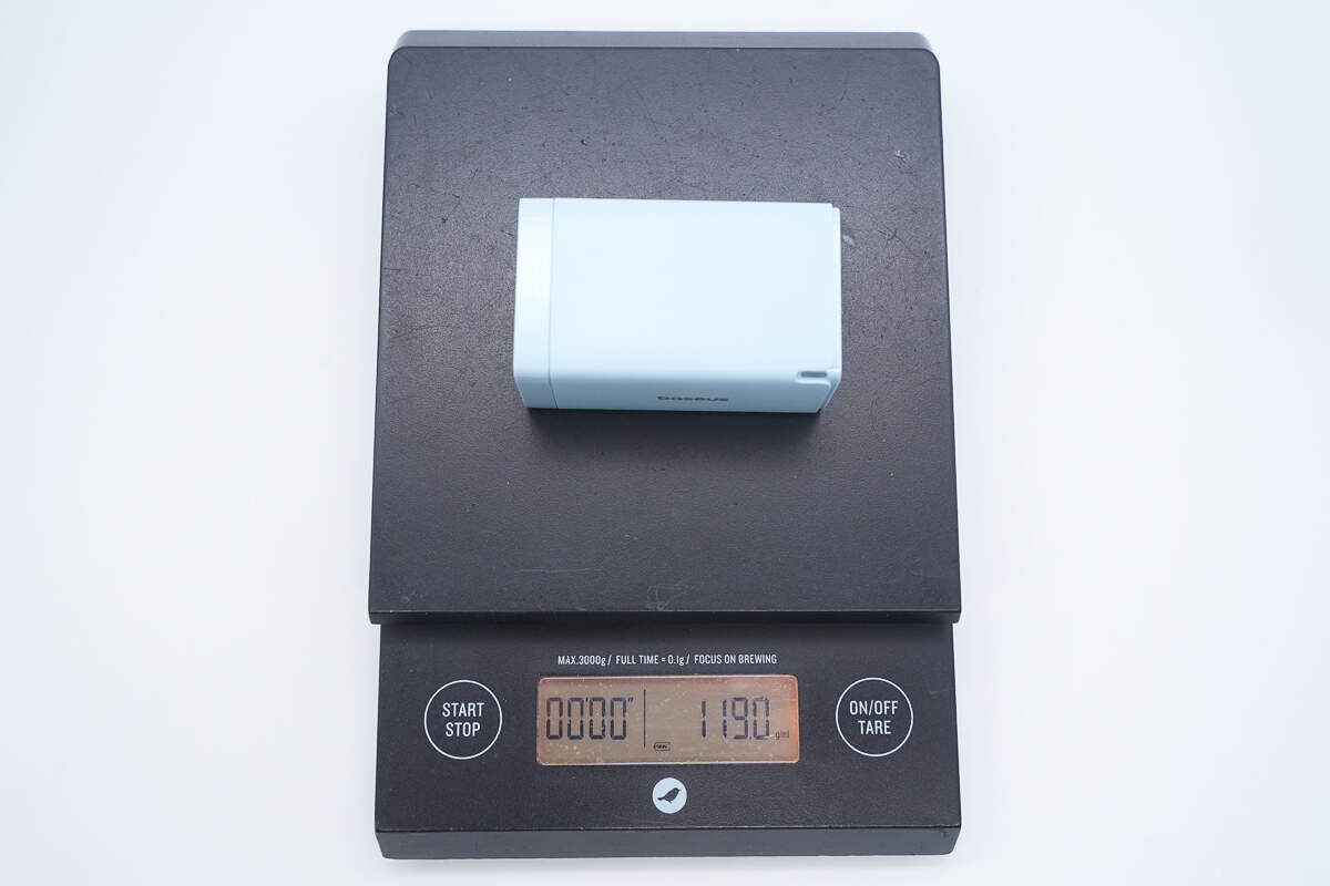
The weight is about 119 g (4.2 oz).
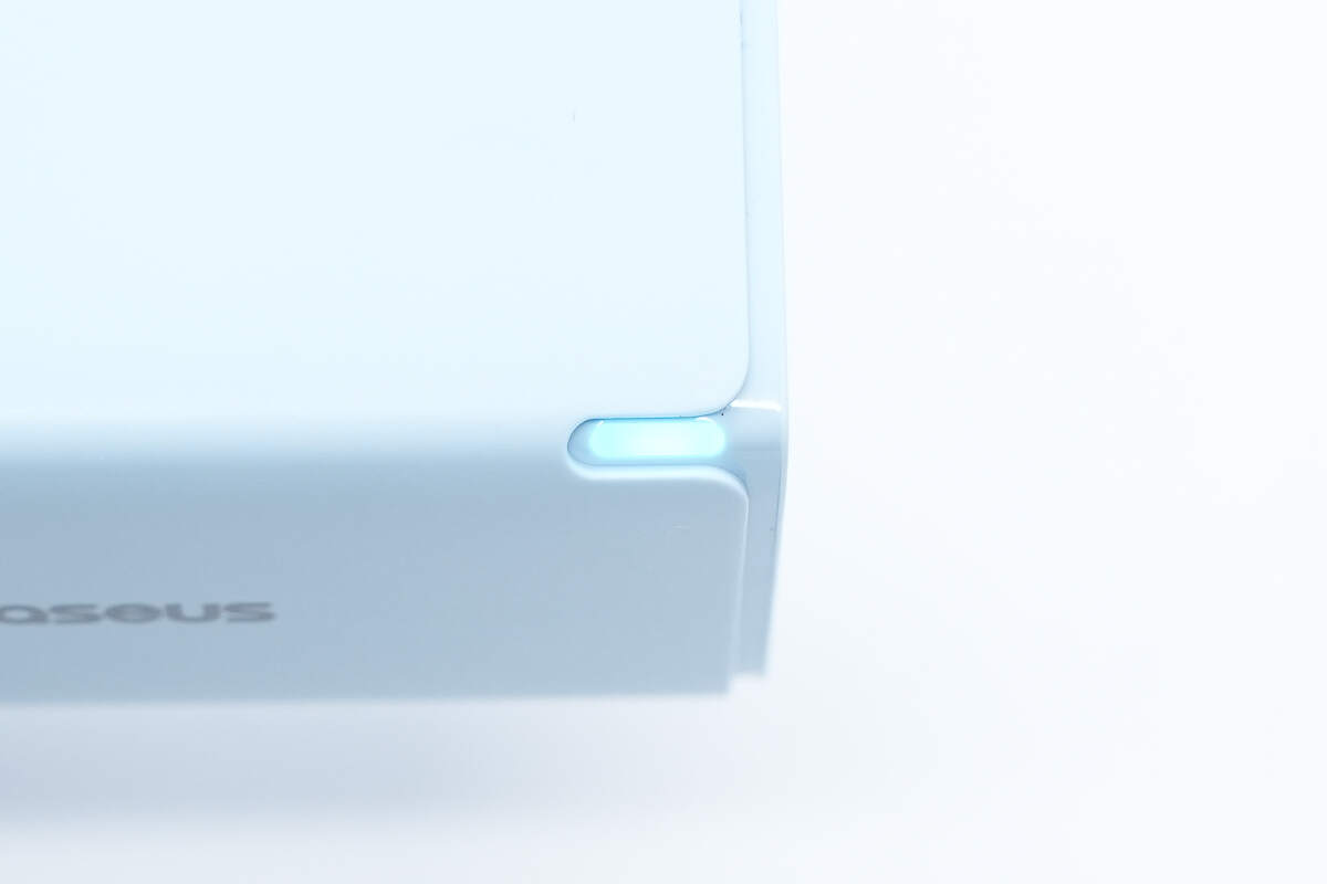
When powered on, a blue indicator light illuminates at the edge of the output end.
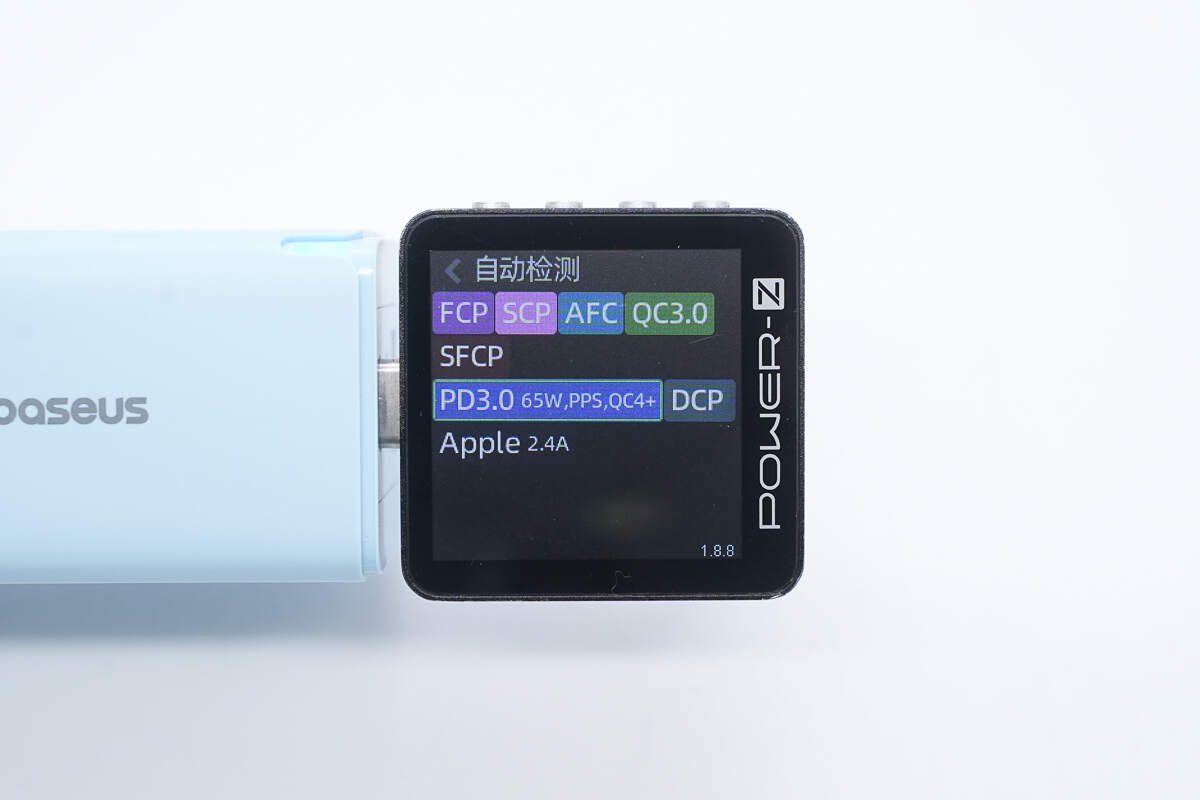
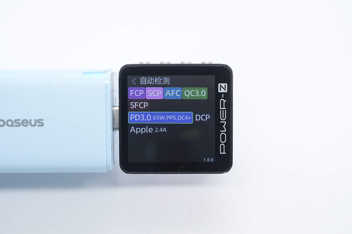
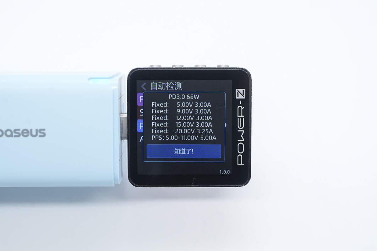
ChargerLAB POWER-Z KM003C shows that the USB-C1 supports FCP, SCP, AFC, QC3.0/4+, SFCP, PD3.0, PPS, DCP, and Apple 2.4A charging protocols.
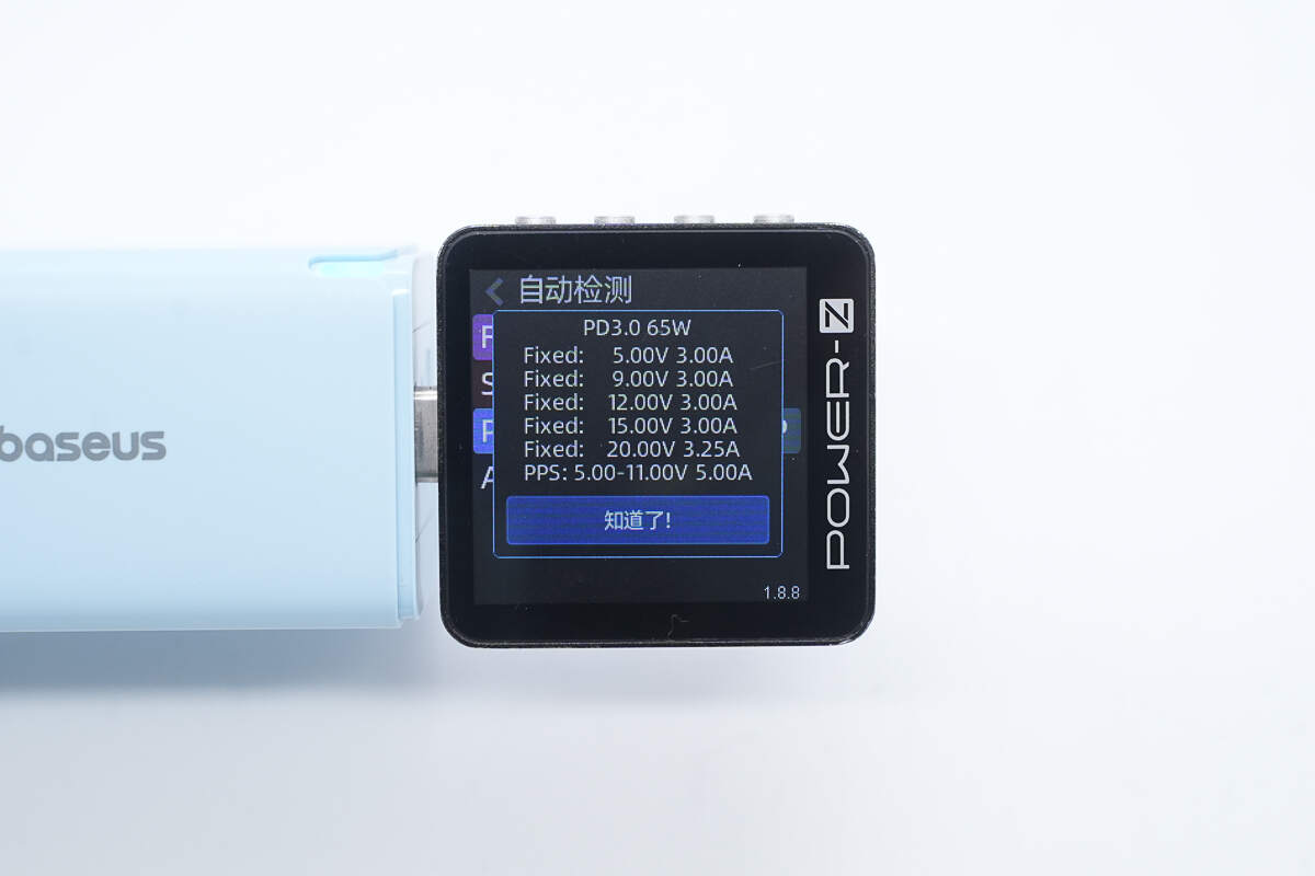
And it has five fixed PDOs of 5V3A, 9V3A, 12V3A, 15V3A, and 20V3.25A. It also has one set of PPS, which is 5-11V5A.
USB-C2 is compatible with the same protocols as USB-C1.
The PDO messages are also identical.
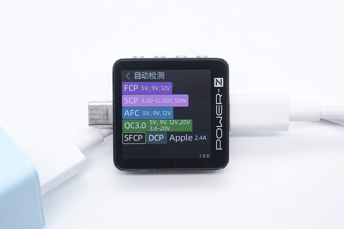
ChargerLAB POWER-Z KM003C shows that the USB-A supports FCP, SCP, AFC, QC3.0, SFCP, DCP, and Apple 2.4A charging protocols.
Teardown
Next, let's take it apart to see its internal components and structure.
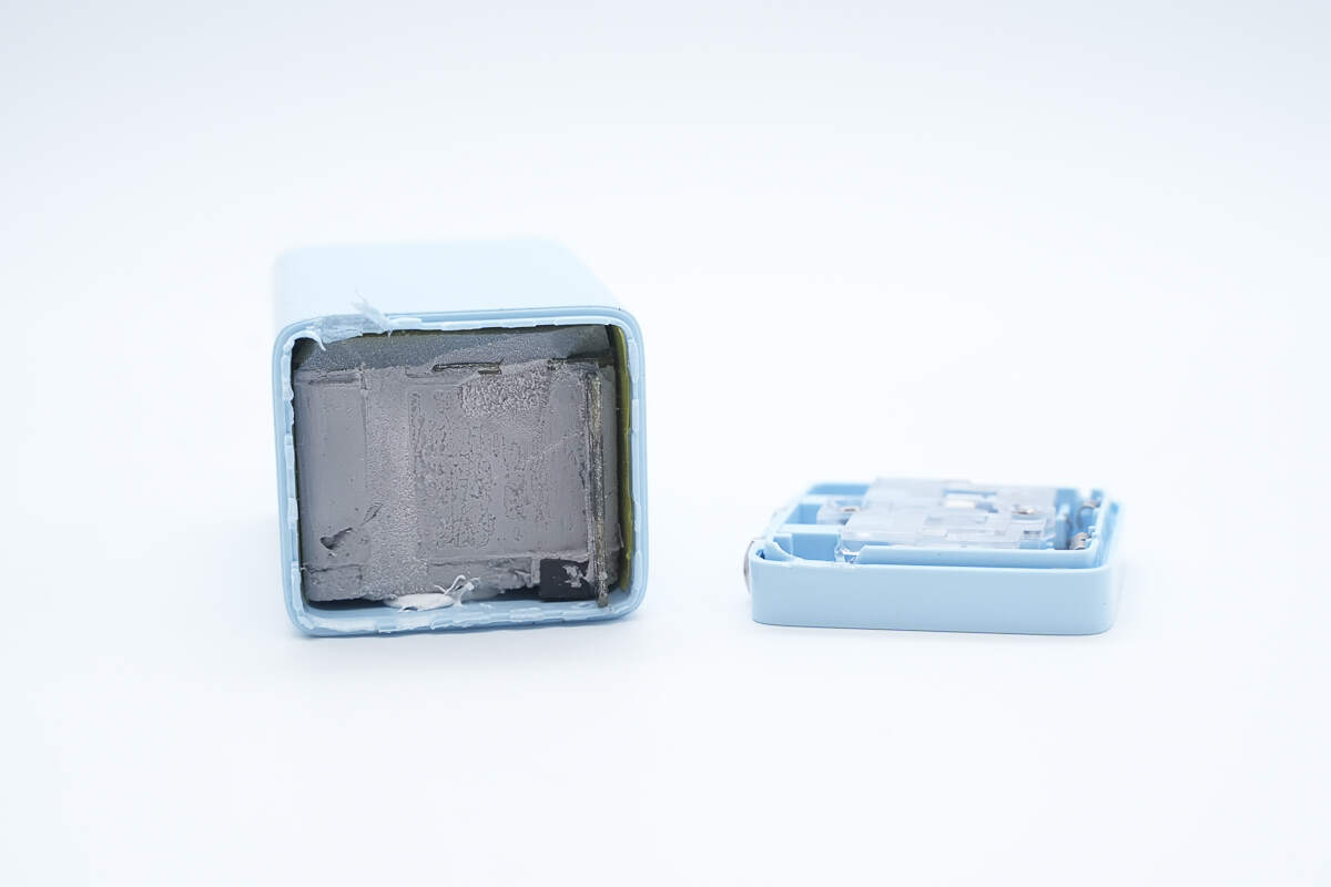
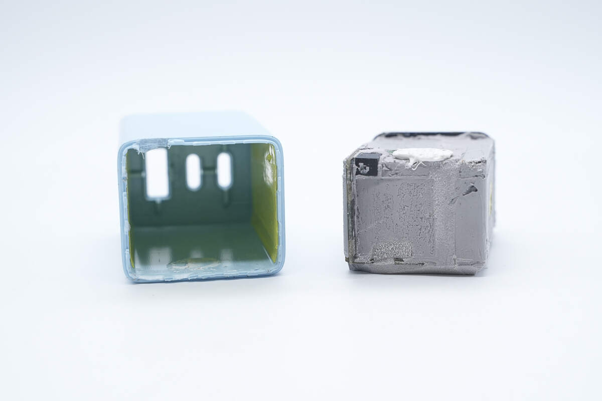
Pry open the casing along the seam.
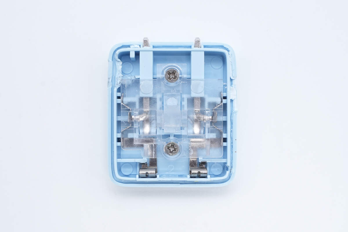
The prongs are secured with a transparent plastic plate and screws, and they make electrical contact with the PCBA module through metal spring contacts.
Remove the PCBA module.
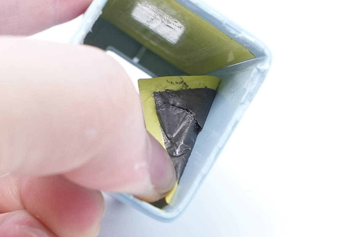
The inner side of the casing is lined with graphite thermal pads and insulating tape.
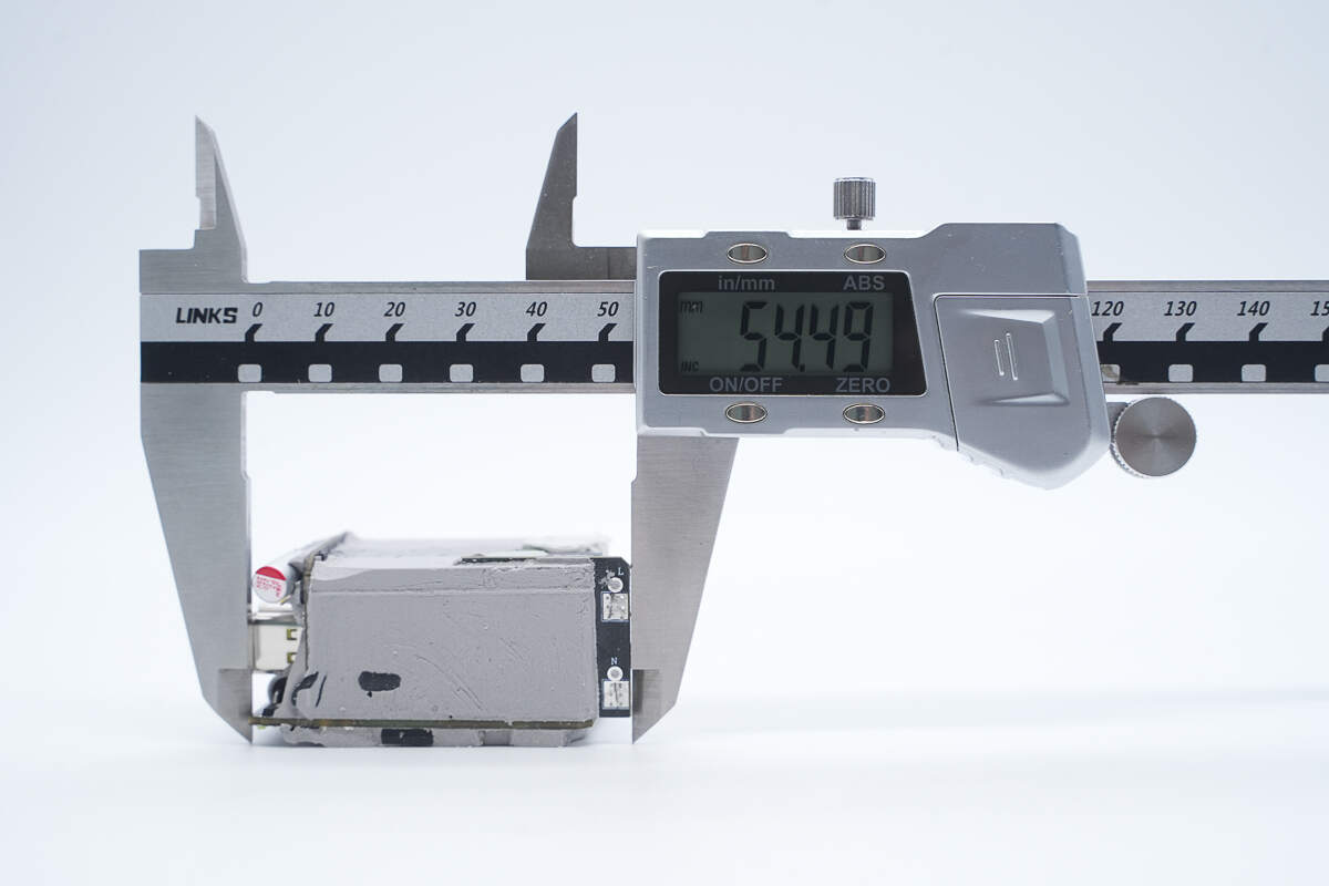
The length of the PCBA module is about 54.49 mm (2.15 inches).
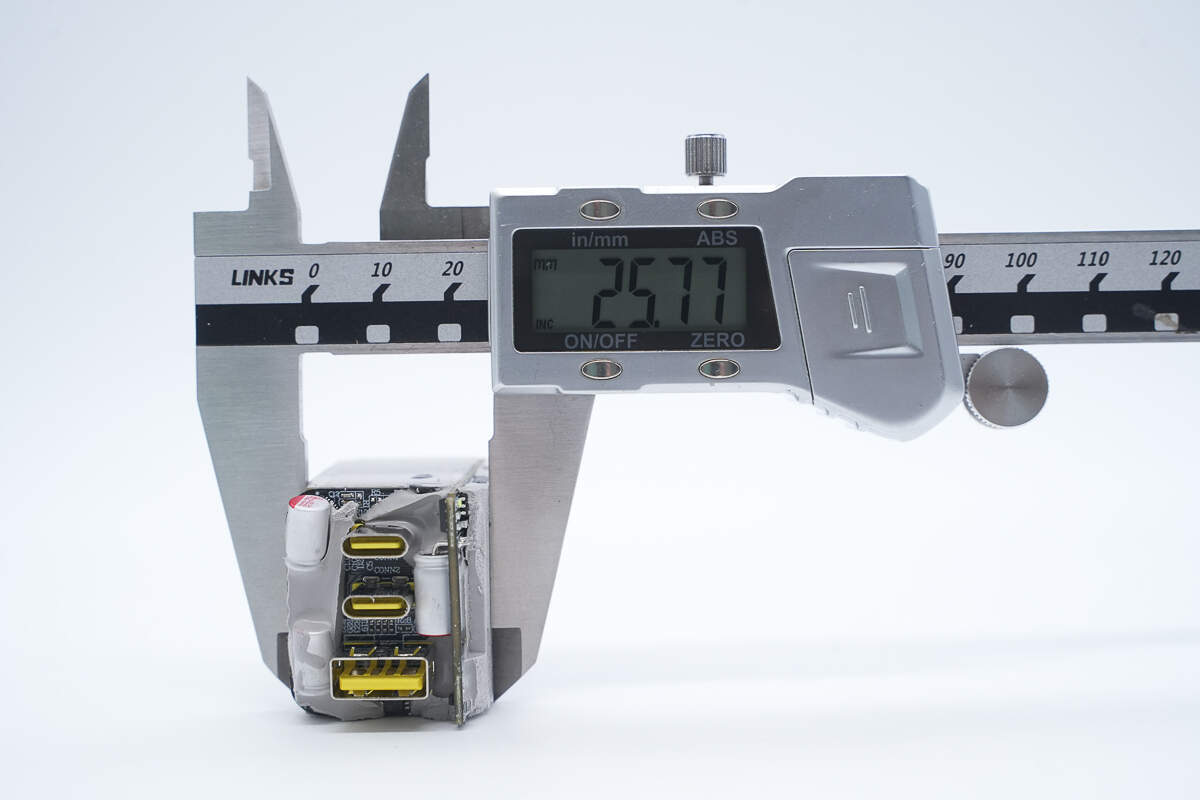
The width is about 25.77 mm (1.015 inches).
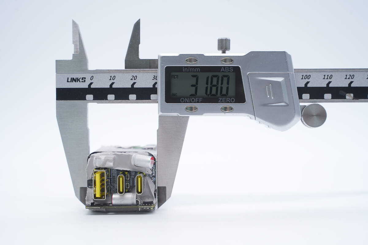
The thickness is about 31.8 mm (1.25 inches).
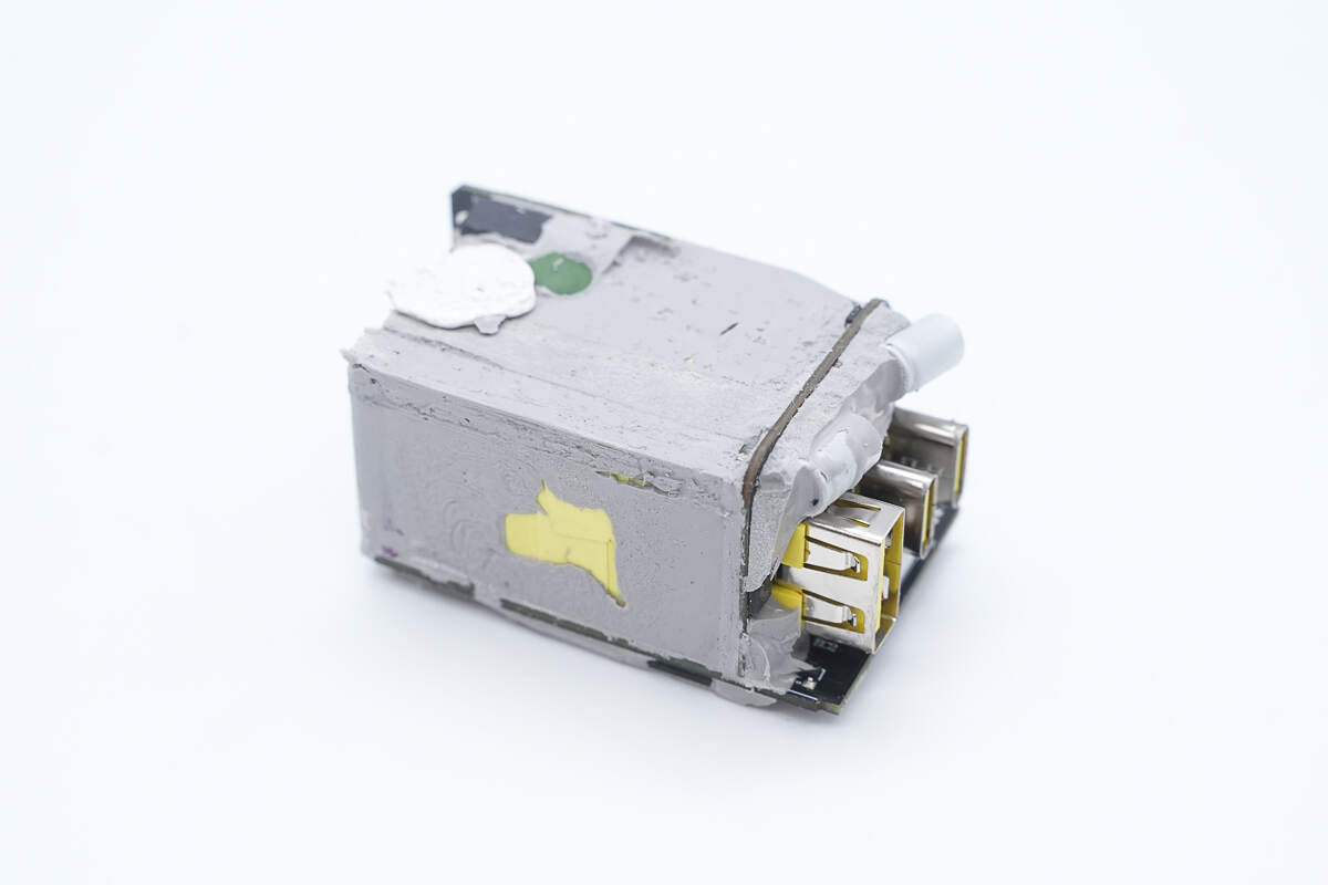
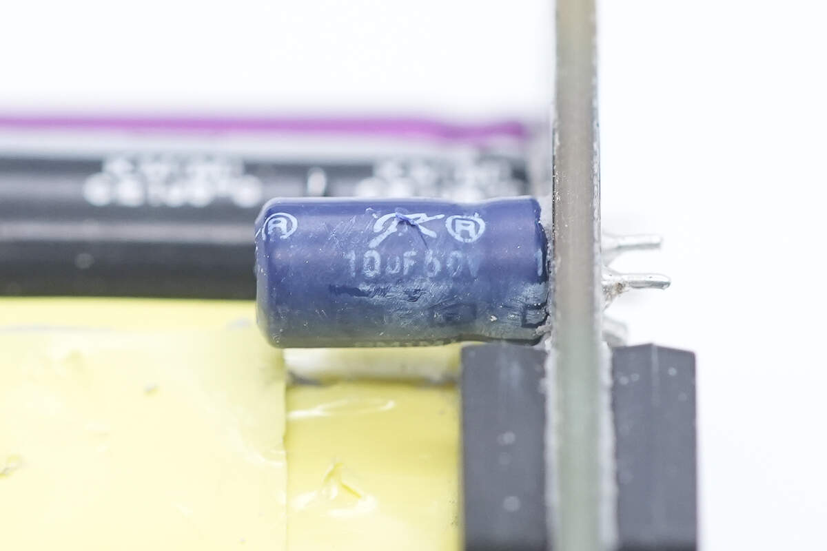
The PCBA module is potted to enhance weather resistance and thermal performance.
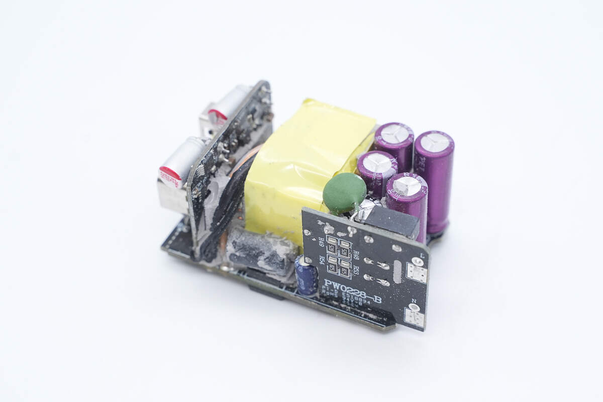
After cleaning off the thermal compound, the module is found to consist of three PCBs.
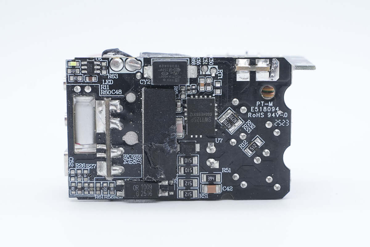
On the back of the module, there are components such as the master control chip, optocoupler, SMD Y capacitor, and synchronous rectifier controller. The primary and secondary sides are isolated by a Mylar sheet.
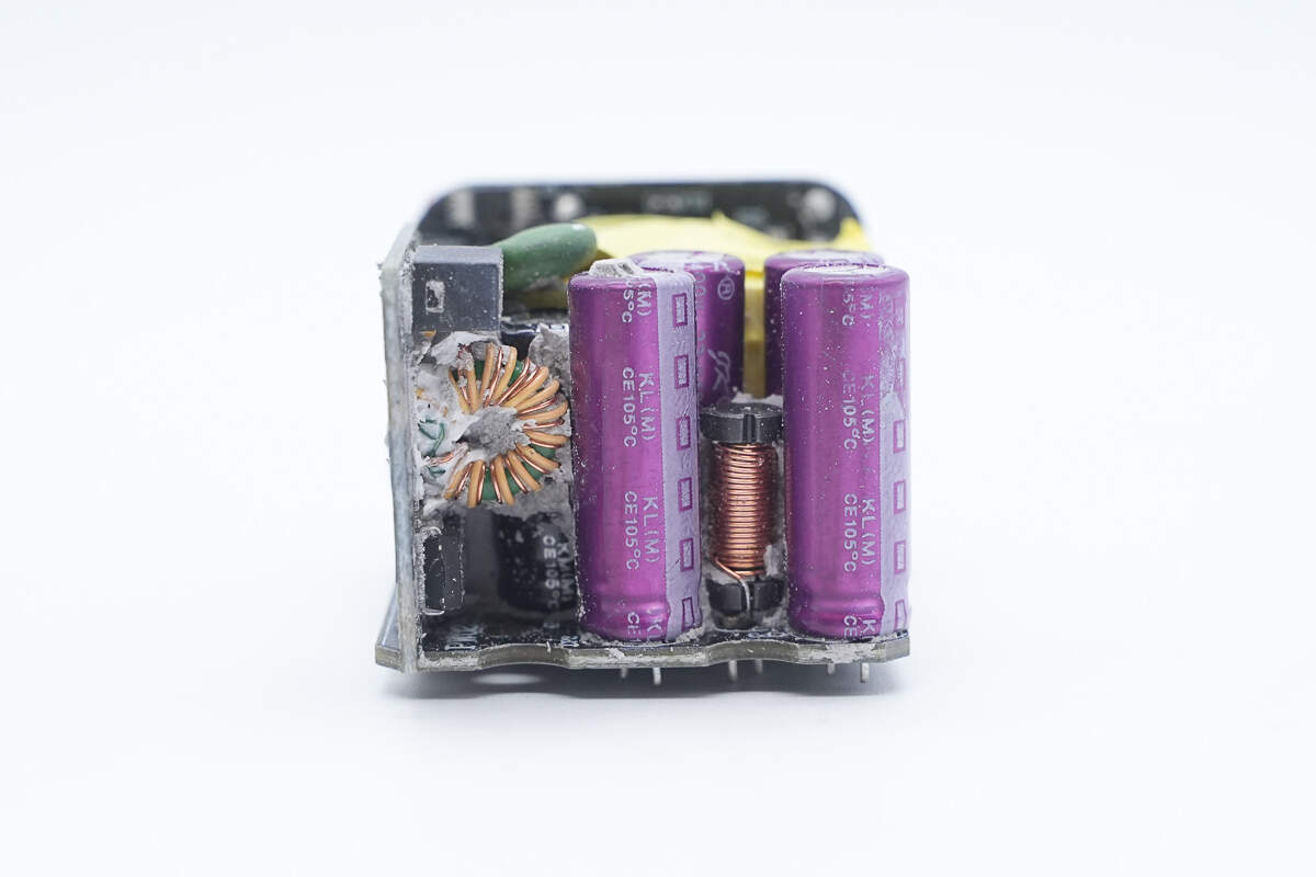
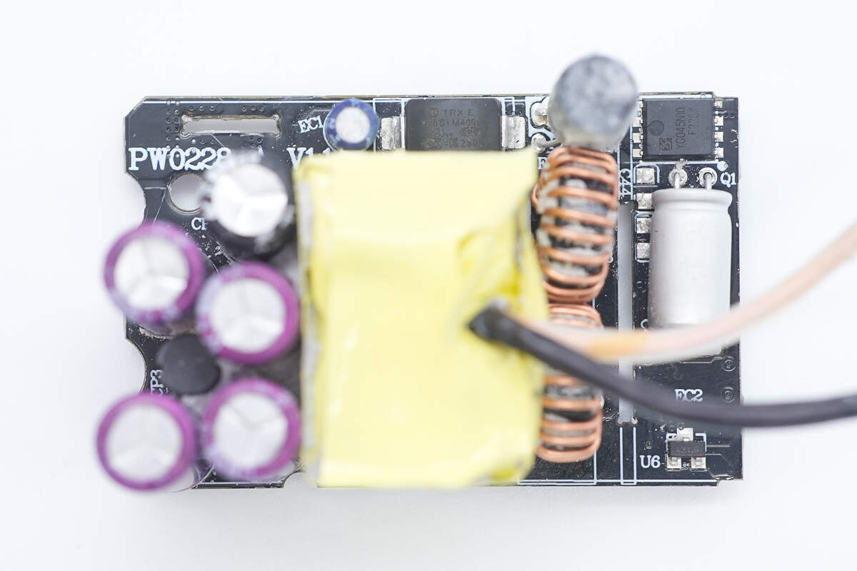
At the front end of the module, there are electrolytic capacitors and an I-shaped inductor. On the left side, there is a small PCB.
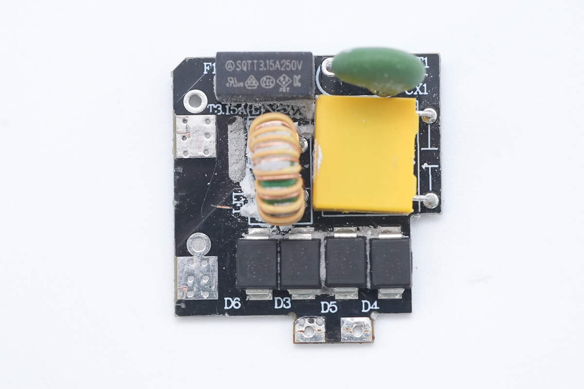
After removing the small PCB, the front side reveals a time-delay fuse, NTC thermistor, safety X2 capacitor, common mode choke, and four Schottky rectifier diodes.
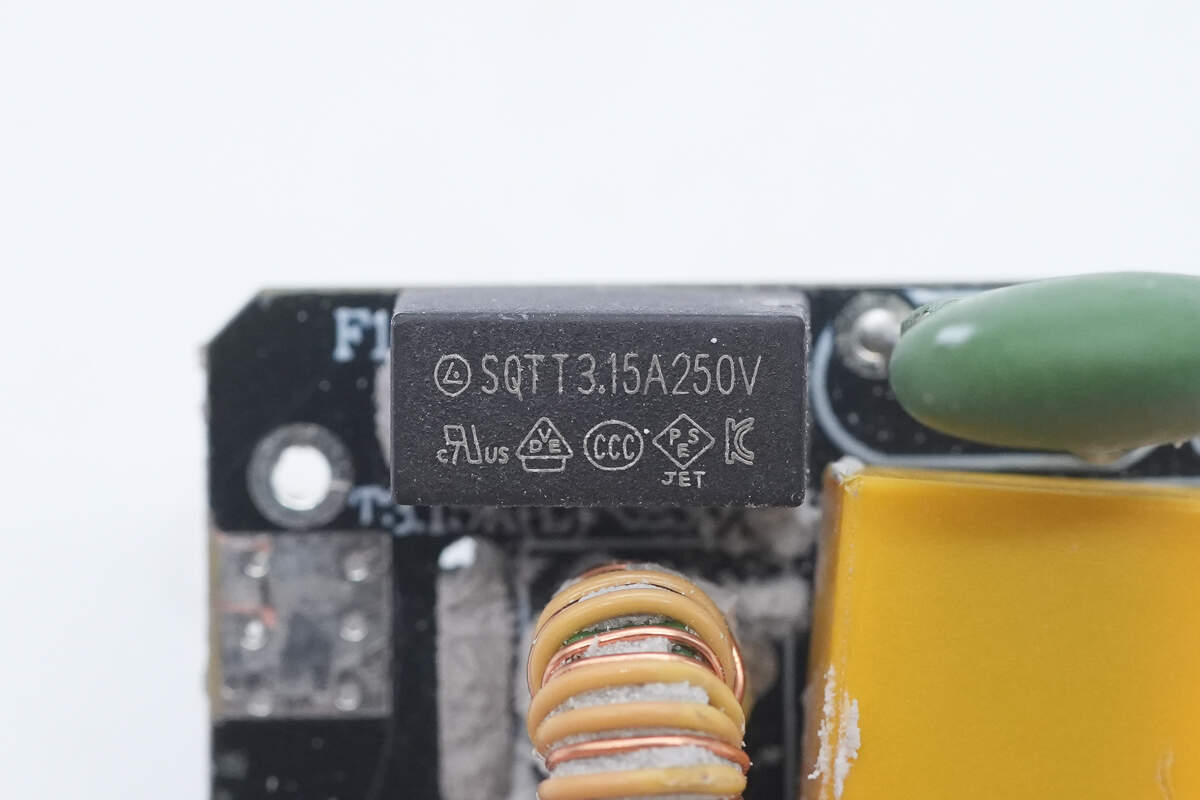
The time-delay fuse is rated at 3.15A, 250V.
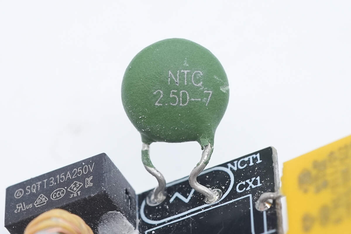
The green NTC thermistor is used to suppress inrush current during power-up.
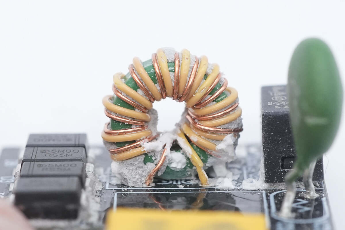
The common mode choke is dual-wound and is used to filter out EMI interference.
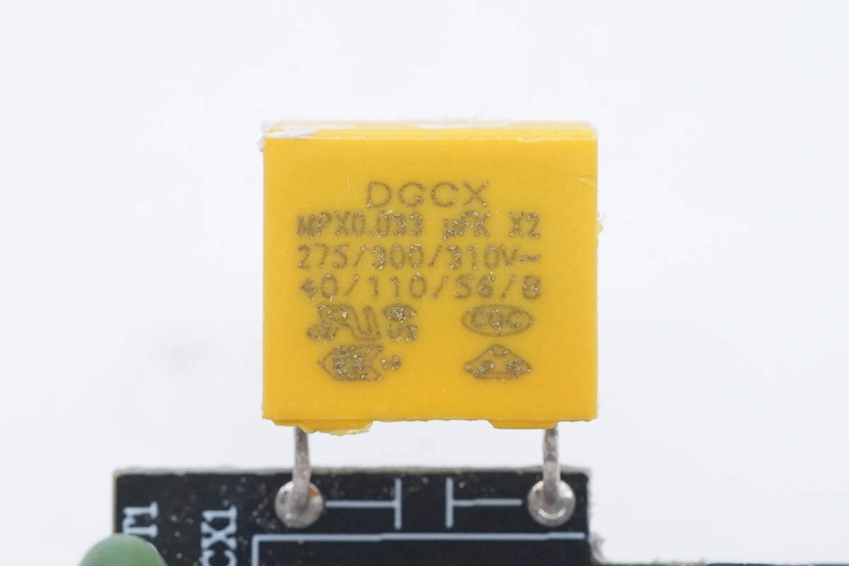
The safety X2 capacitor is from DGCX. 0.33μF.
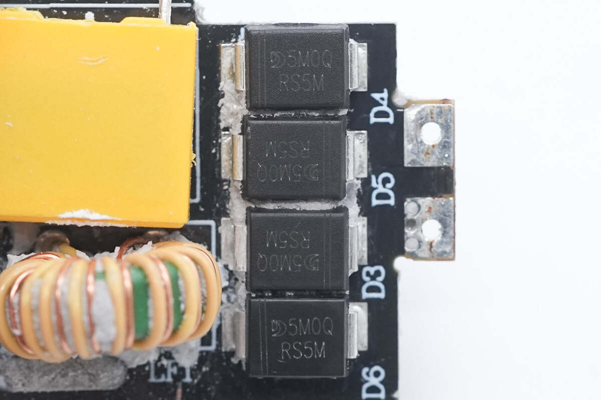
The four 5M0Q diodes form a bridge rectifier.
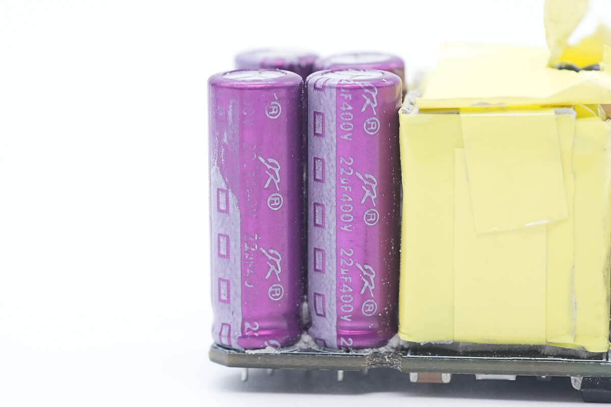
The four purple electrolytic capacitors are from JK, each rated at 400V 22μF.
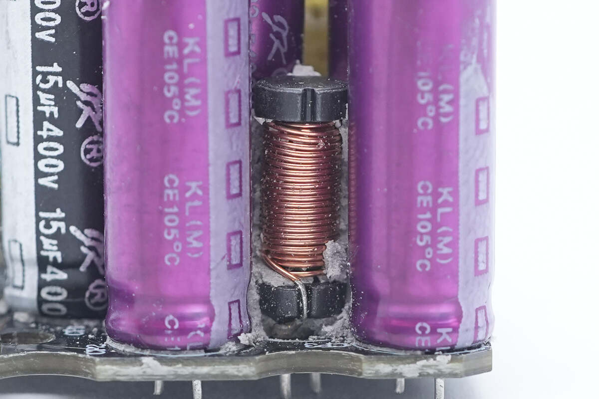
Close-up of the I-shaped inductor.
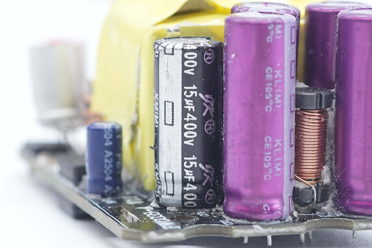
The black electrolytic capacitor is also from JK, with a specification of 400V 15μF.
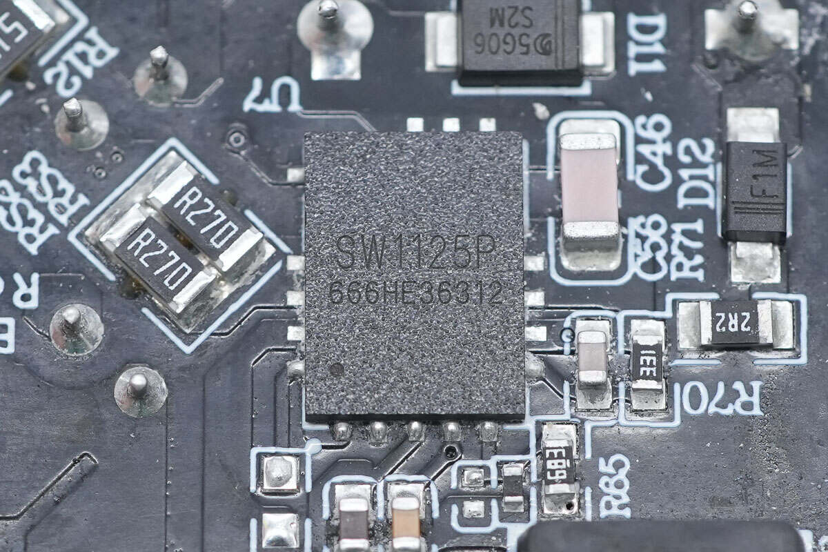
The master control chip is the iSmartWare SW1125P, an integrated GaN IC. It features a 700V voltage tolerance and a 260mΩ on-resistance GaN FET, functioning as a high-frequency quasi-resonant flyback converter. It also integrates a 700V high-voltage startup circuit, line-voltage brown-in/brown-out detection, and X-capacitor discharge functionality.
The SW1125P operates in valley-switching mode with valley-lock, reducing switching losses. It includes a frequency jitter function to improve EMI performance. The chip supports burst mode, automatically entering it under light-load conditions to improve efficiency. Standby power consumption is below 50mW, complying with Level VI energy efficiency standards.
It supports an ultra-wide input voltage range of 8–90V and a maximum switching frequency of 300kHz. The chip adopts a thermally enhanced QFN 6×8 package, which allows heat dissipation through vias to reduce temperature rise, optimize PCB layout, and simplify thermal design.
It also features multiple comprehensive protection functions and supports external NTC thermistor input for real-time charger temperature monitoring, enabling a robust and well-rounded protection scheme.
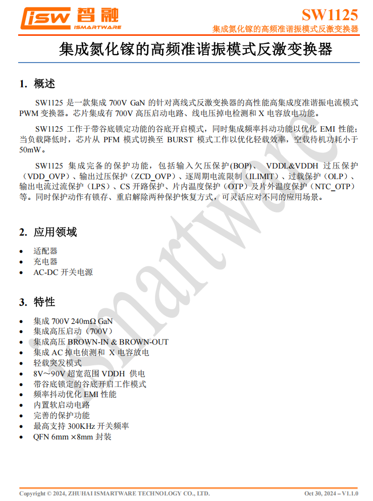
The capacitor supplying power to the master control chip is from JK, with a specification of 50V 10μF.
The transformer is wrapped with insulating tape.
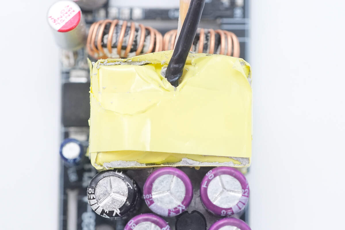
Close-up of the OR 1009 optocoupler.
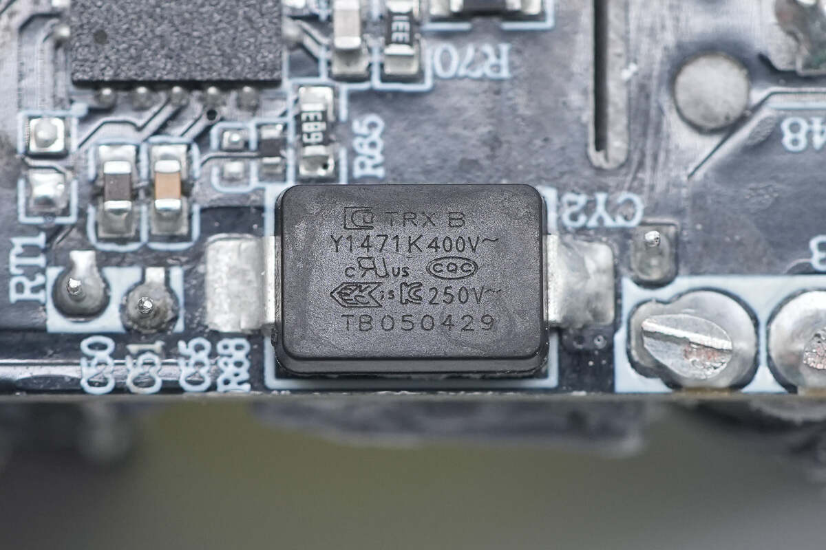
The SMD Y capacitor is from TRX. Its small size and light weight are suitable for high-density power products such as GaN fast chargers. The part number is TMY1471K.
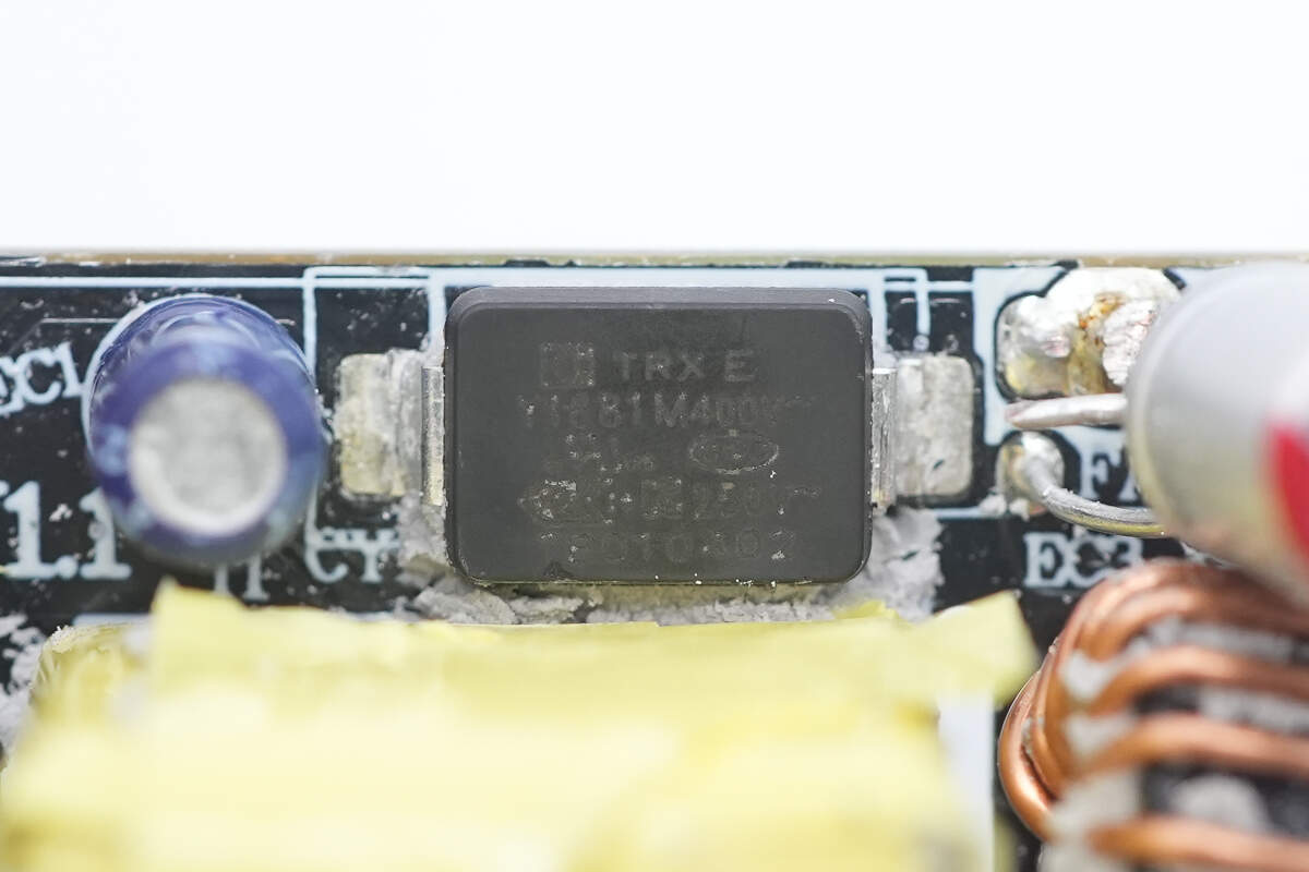
Another SMD Y capacitor is also from TRX, with the part number TMY1681M.
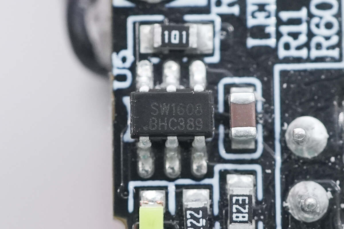
The synchronous rectifier controller is the iSmartWare SW1608, a high-performance controller designed for driving secondary-side synchronous rectifiers in offline flyback converters. It comes in a compact SOT23-6 package and supports a 6V or 9V VCC power supply. Notably, it features a self-powered VCC capability, eliminating the need for an auxiliary winding and supporting a wide output voltage range. Used in conjunction with a MOSFET to replace traditional Schottky rectifier diodes, the SW1608 can significantly improve overall system efficiency.
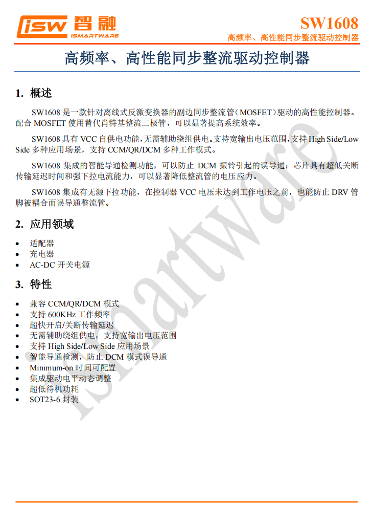
The SW1608 supports operating frequencies up to 600kHz and is compatible with both High Side and Low Side application scenarios. It also supports multiple operating modes, including CCM, QR, and DCM.
Additionally, it features an intelligent turn-on detection mechanism that effectively prevents false triggering caused by DCM ringing. With ultra-low shutdown propagation delay and strong pull-down drive capability, the SW1608 significantly reduces voltage stress on the rectifier MOSFET, enhancing reliability and performance in high-efficiency power supply designs.
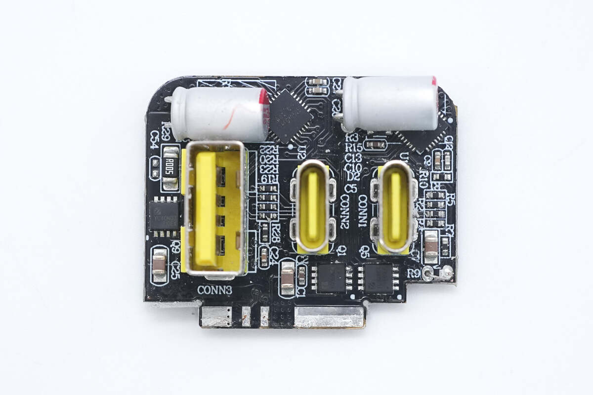
A secondary step-down PCB is soldered at the output end.
After removing the small PCB, the secondary side of the main PCB reveals the synchronous rectifier, solid capacitor, and buck inductors for the two secondary step-down circuits.
The front side of the secondary step-down PCB is equipped with buck protocol chips, synchronous buck MOSFETs, solid capacitors, and output VBUS MOSFETs.
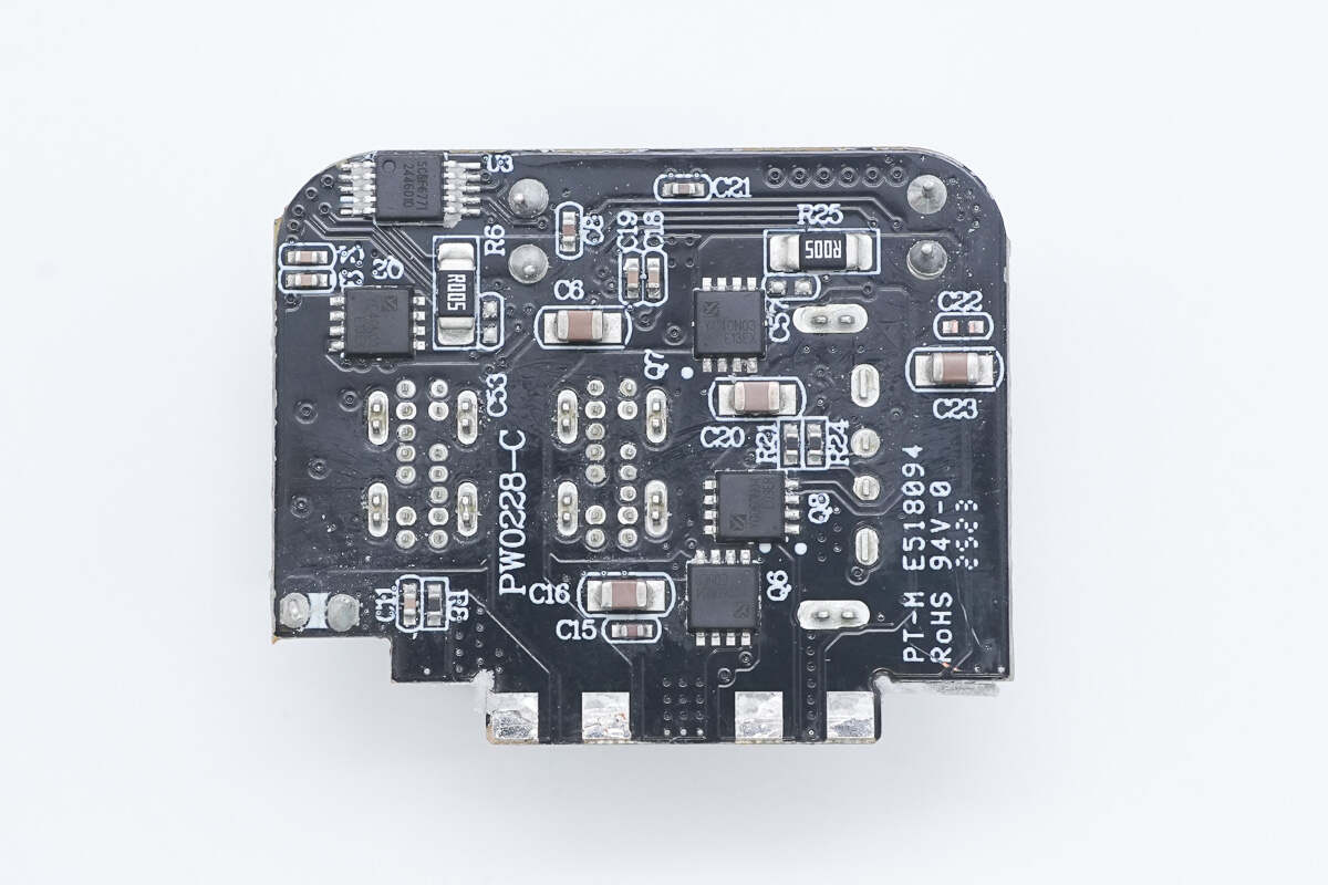
On the back side, there are the MCU, synchronous buck MOSFETs, and VBUS MOSFETs.
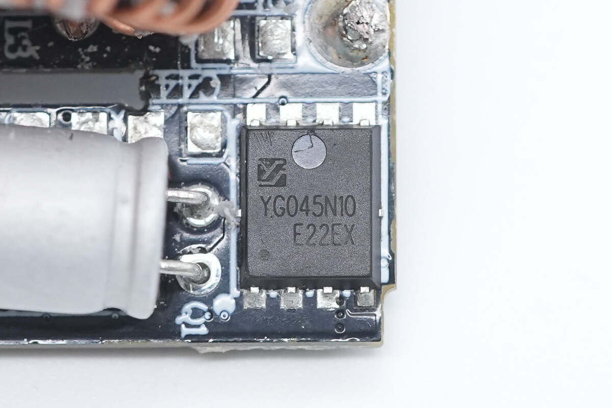
The synchronous rectifier is marked with YG045N10.
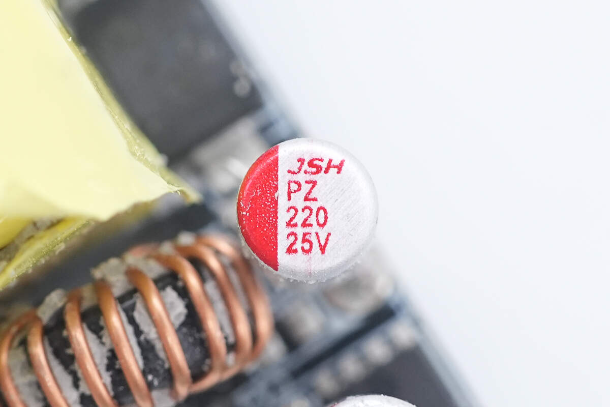
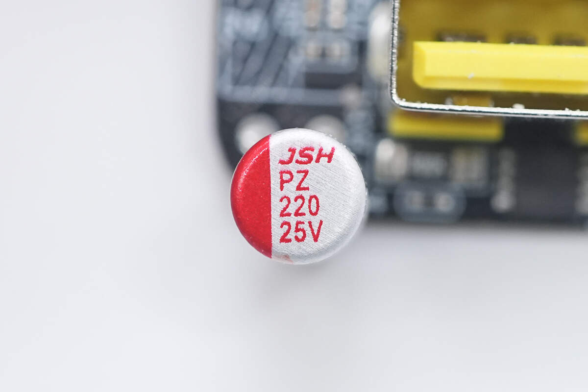
The output solid capacitor is from JSH, with a specification of 25V 220μF.
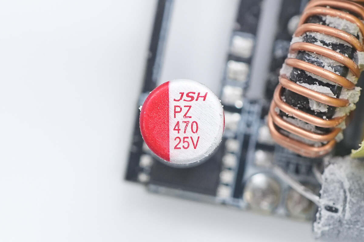
The other output solid capacitor is rated at 25V 470μF.
Close up of the thermistor.
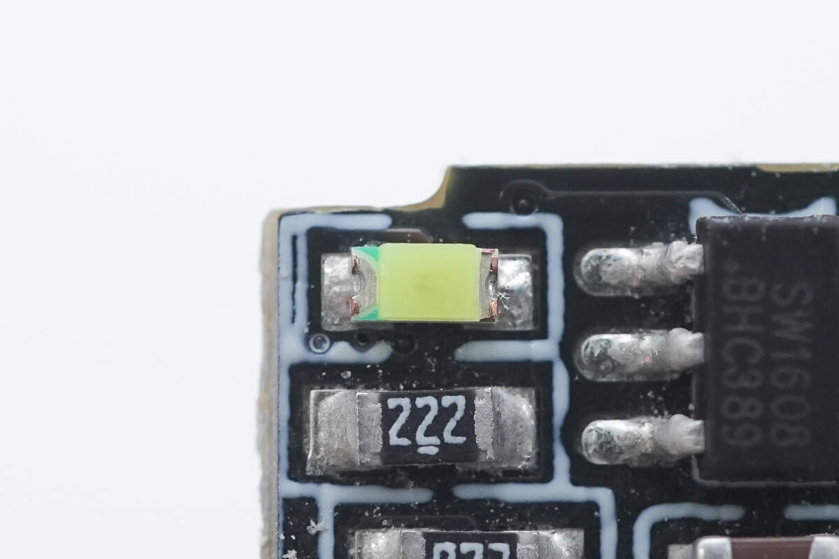
Close-up of the LED indicator light.
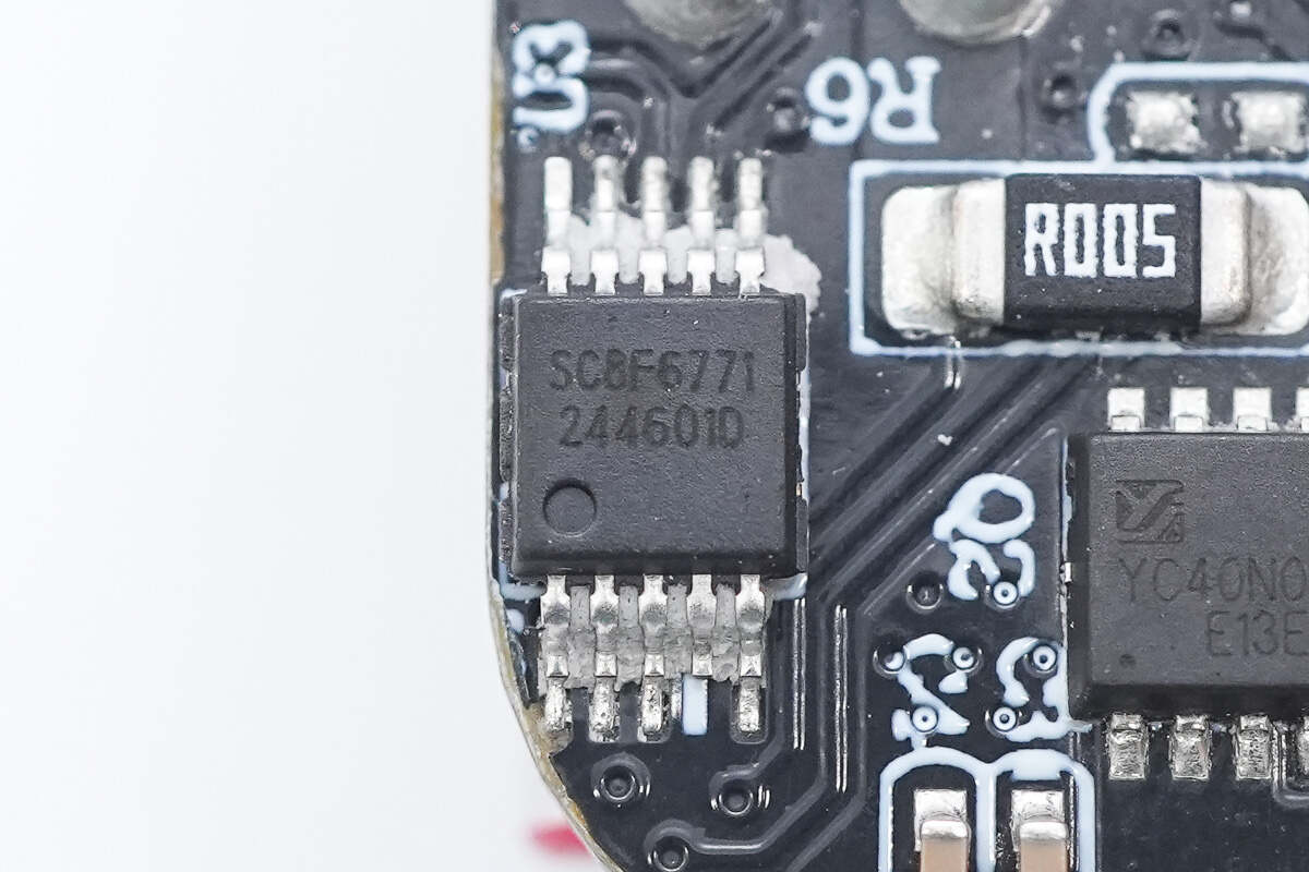
The MCU is from Cmsemicon, model SC8F6771. It is an enhanced flash 8-bit CMOS microcontroller with 4KB of internal FLASH memory and 256 bytes of RAM. It operates at a clock speed of 16MHz and comes in an MSOP10 package.
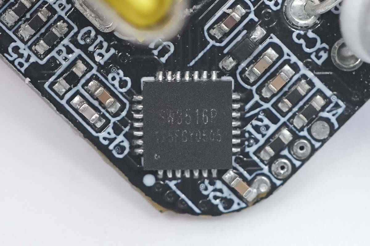
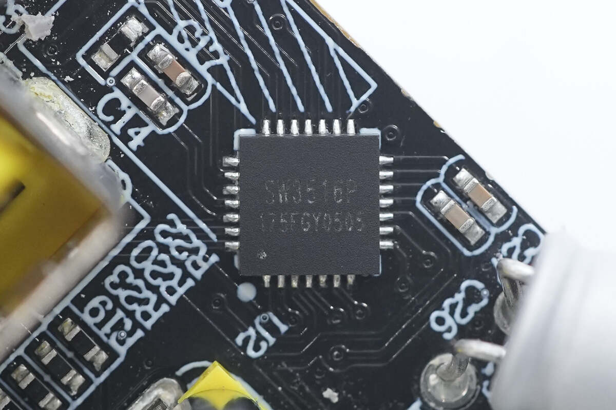
The buck protocol IC for the USB-C1 port is the iSmartWare SW3516P. This is a highly integrated dual-port fast-charging chip that supports fast charging output on either port A or C. It features independent current limiting for both ports and integrates a 5A high-efficiency synchronous buck converter.
The SW3516P supports multiple fast-charging protocols, including PPS, PD, QC, AFC, FCP, SCP, PE, and SFCP. It delivers a maximum PD output power of 100W, supports CC/CV modes, and incorporates dual-port management logic. With minimal external components required, it enables a complete, high-performance multi-protocol fast-charging dual-port solution.
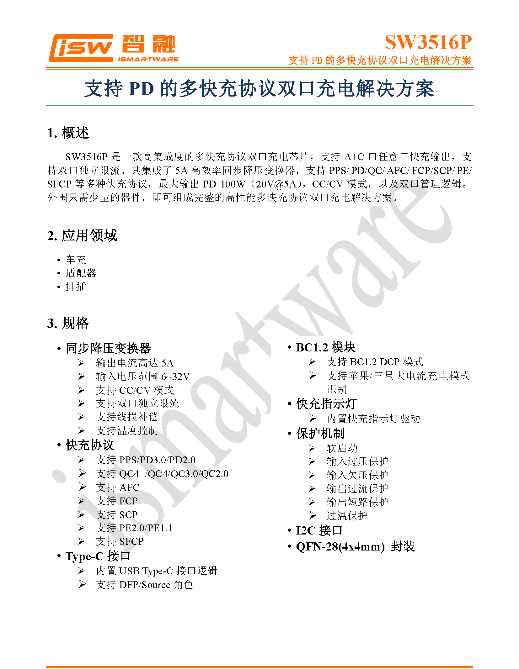
Here is the information about iSmartWare SW3516P.
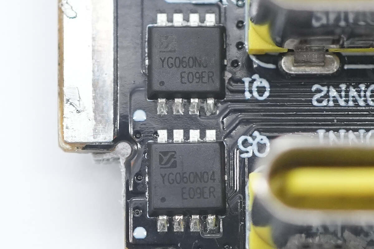
The synchronous buck MOSFETs are marked with YG060N04.
The buck protocol chips for the other two ports also use the iSmartWare SW3516P.
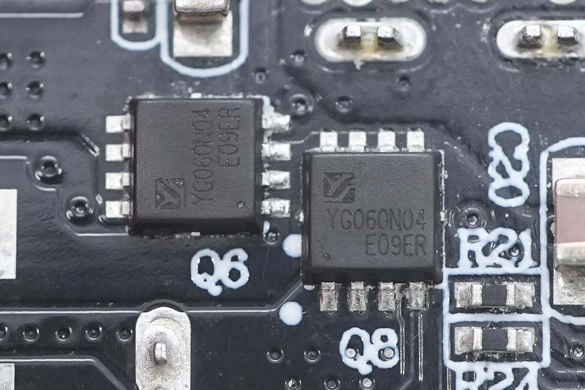
The paired synchronous buck MOSFETs are marked with YG060N04.
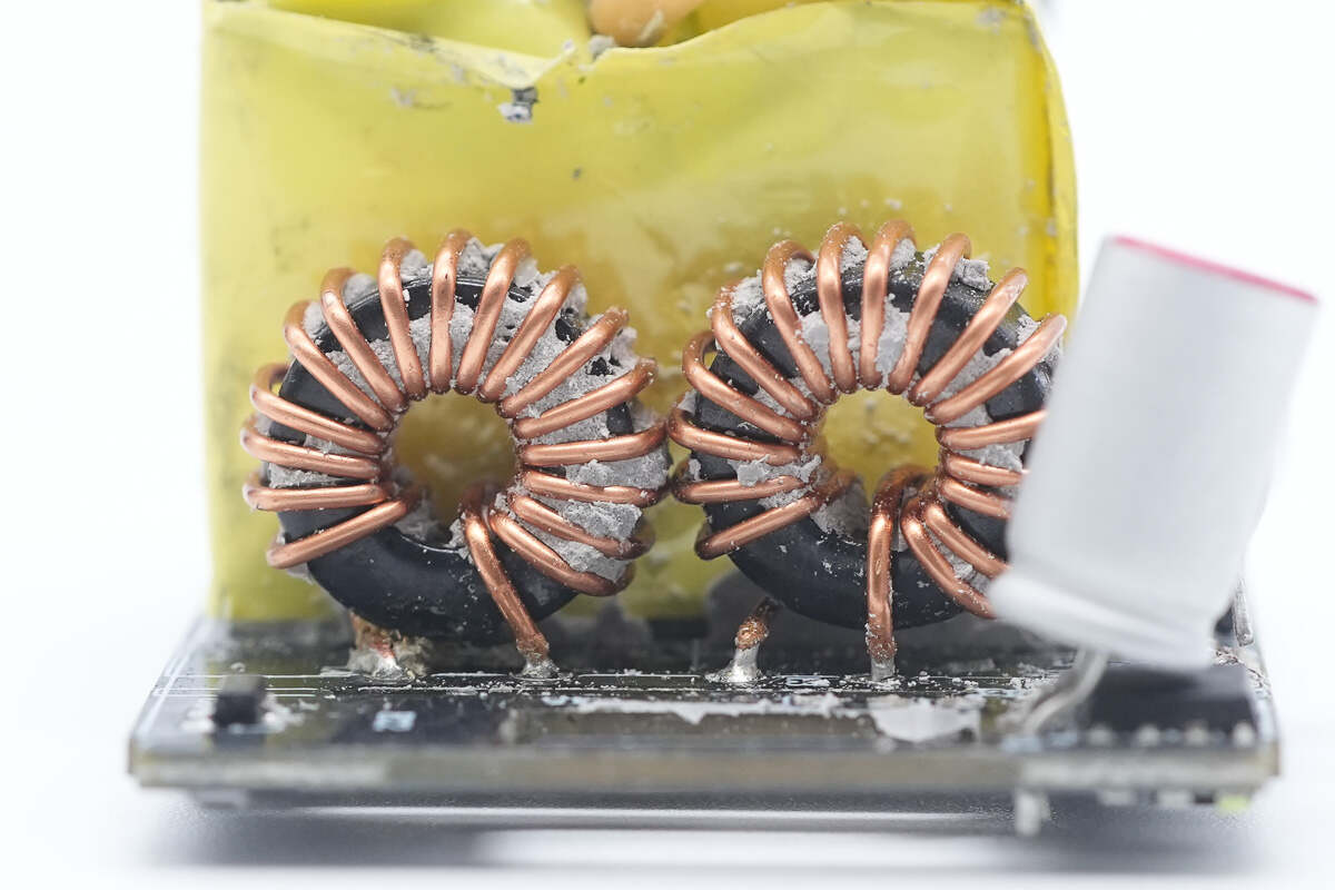
Close-up of the two buck inductors.
The secondary step-down output solid capacitors are also from JSH, each rated at 25V 220μF.
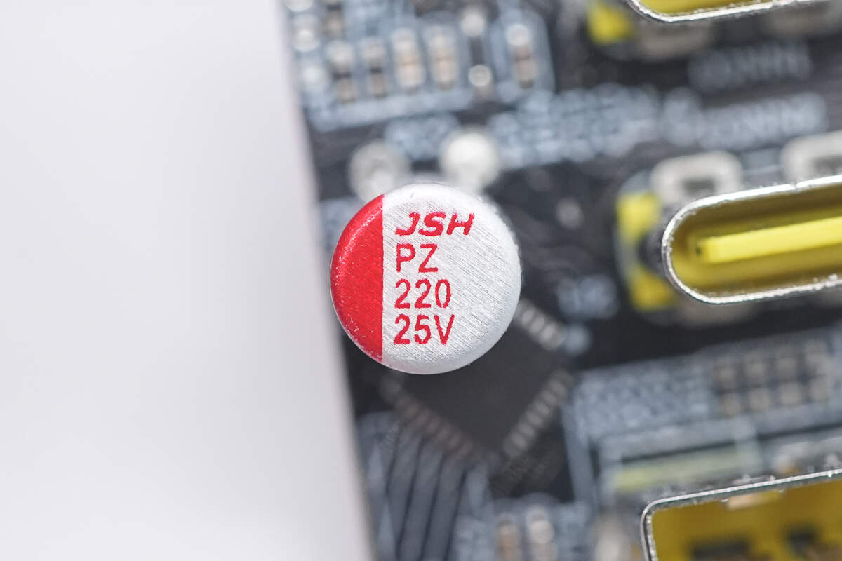
The other capacitor has the same part number.
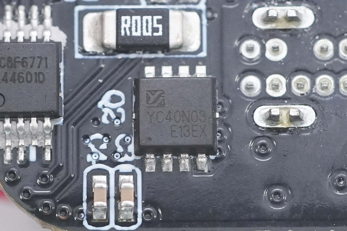
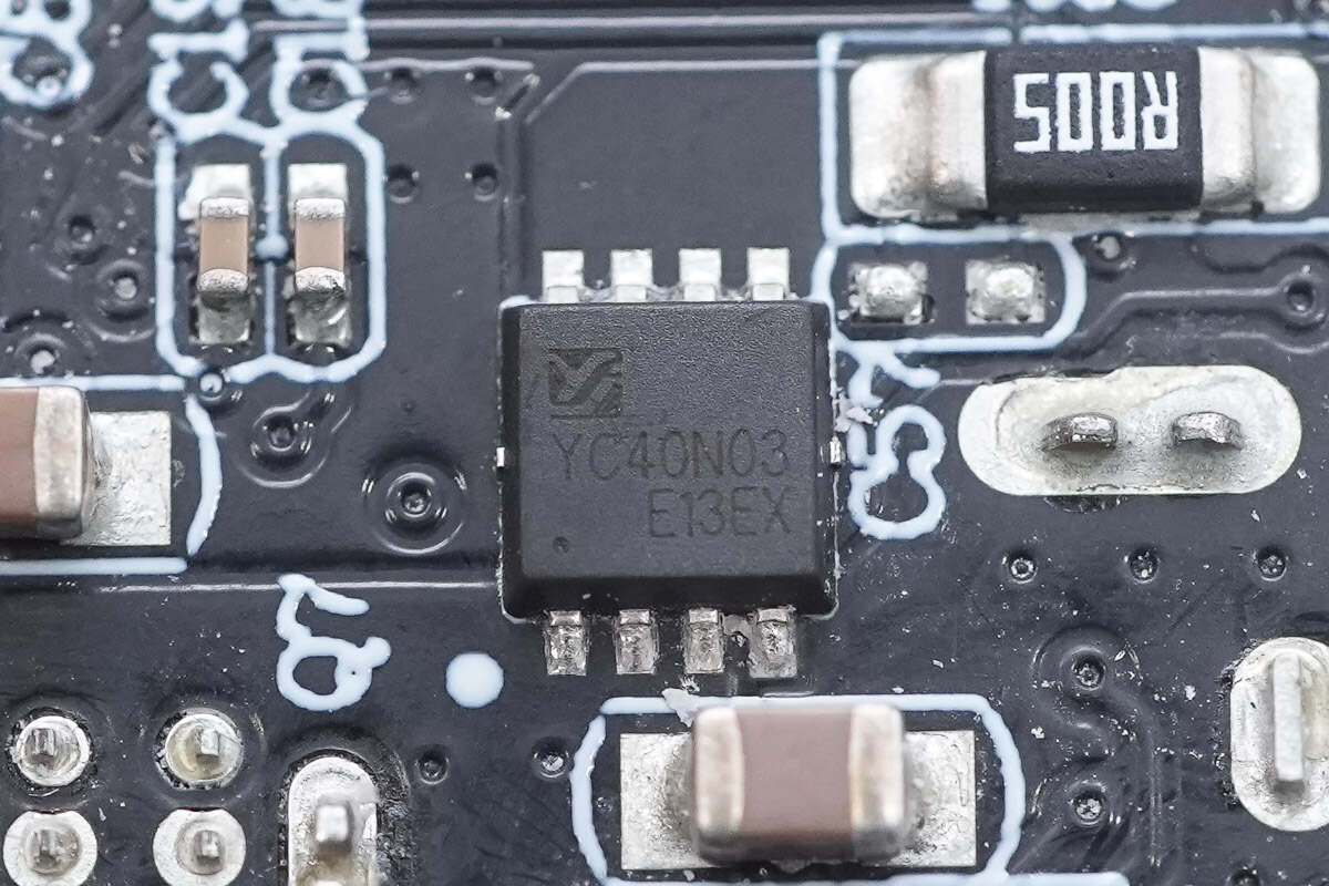
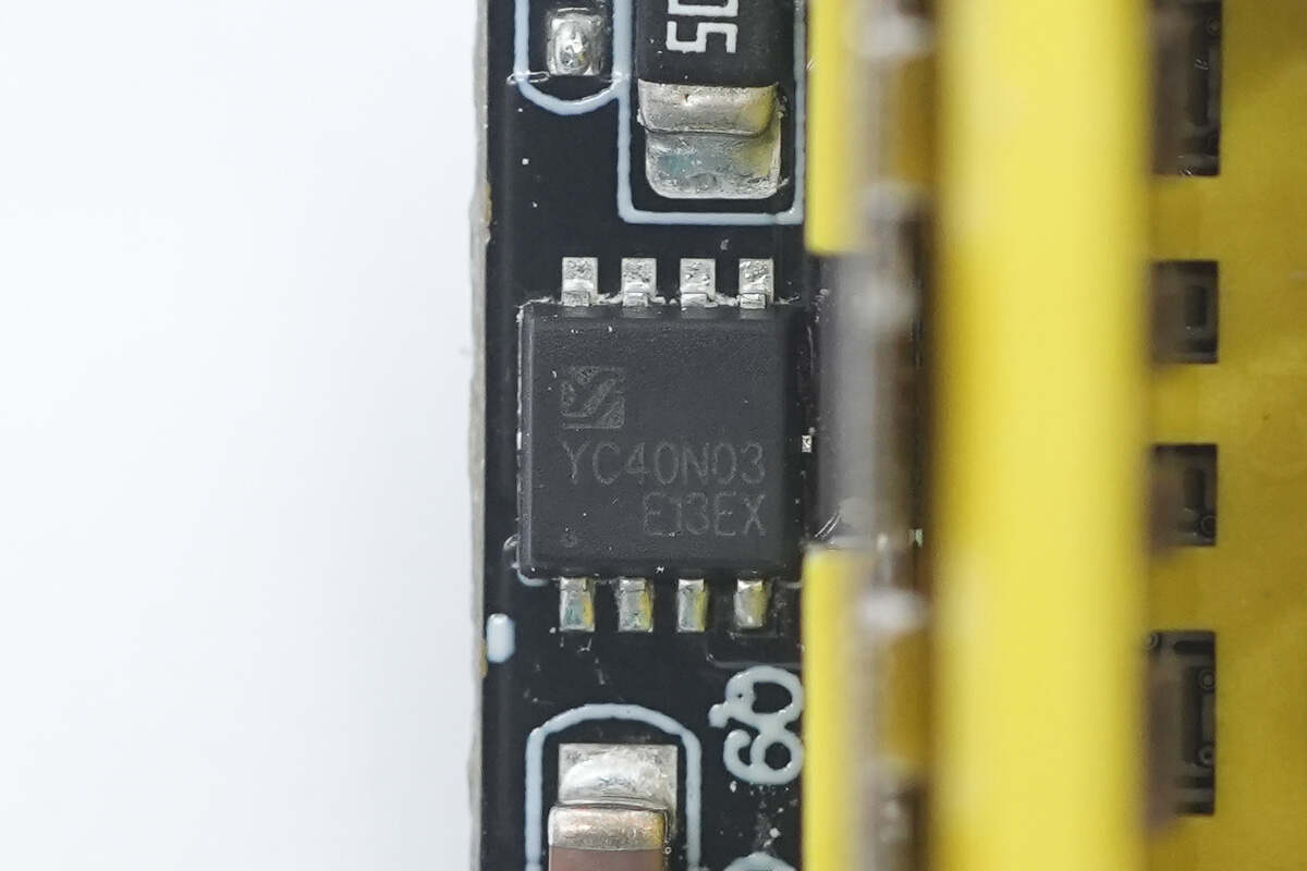
The VBUS MOSFETs for all three ports are YC40N03ADE, rated for 30V with an on-resistance of 8.5mΩ, and come in a PDFN 3×3 package.
Close-up of the VBUS MOSFET for the other USB-C port.
Close-up of the VBUS MOSFET for the USB-A port.
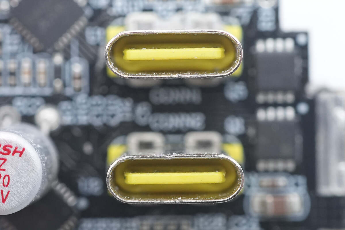
Close-up of the USB-C sockets.
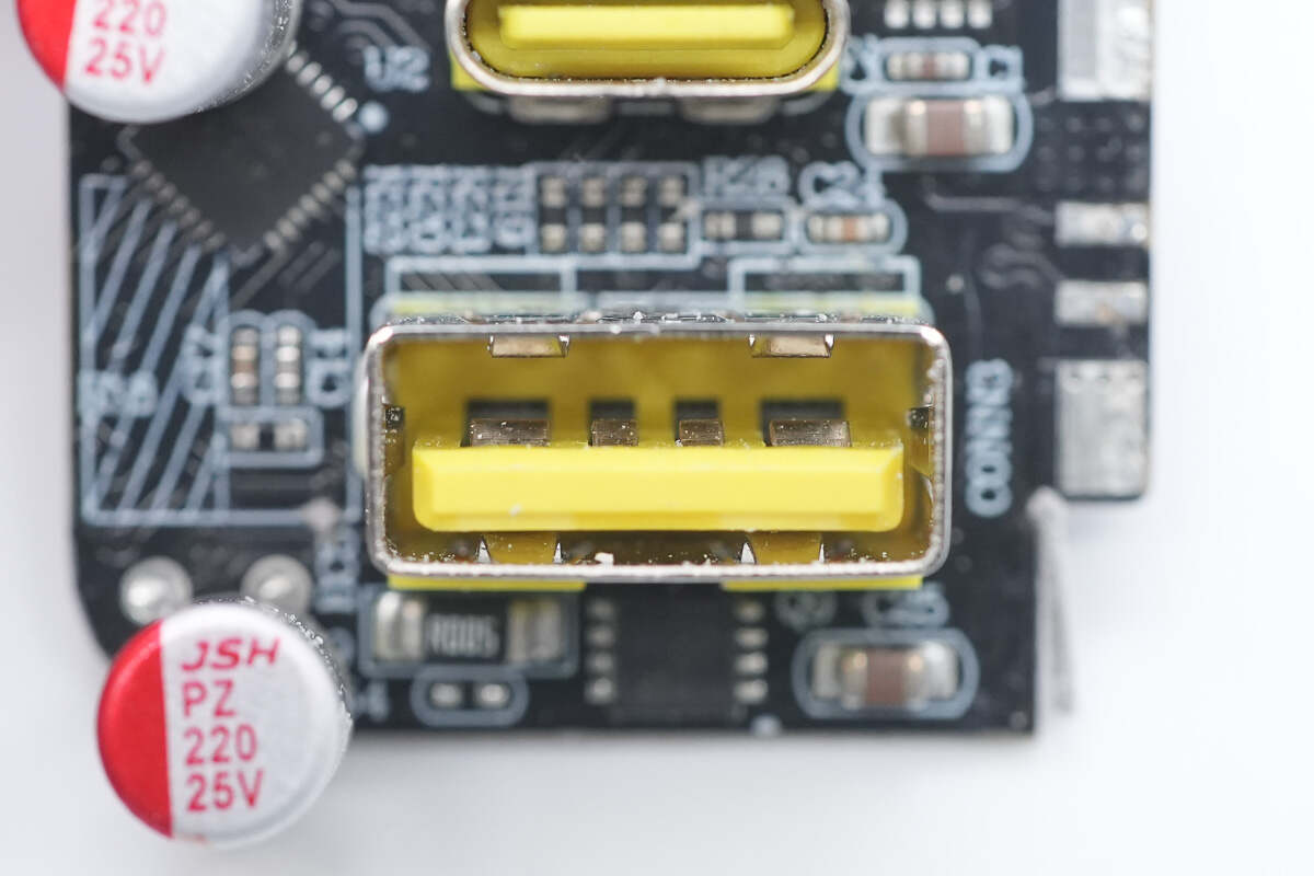
Close-up of the USB-A socket.

Well, those are all components of the Baseus 65W GaN5 Pro Charger.
Summary of ChargerLAB
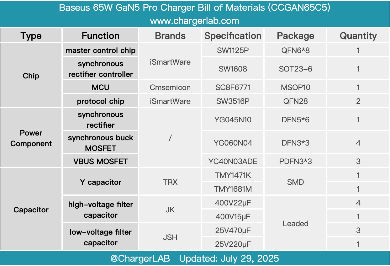
Here is the component list of the Baseus 65W GaN5 Pro Charger for your convenience.
This charger is available in black, white, and blue color options. With compact dimensions of just 61 × 36 × 32 mm and foldable prongs, it is highly portable. It features two USB-C ports and one USB-A port, supporting up to 65W and 60W fast charging. It is compatible with multiple fast-charging protocols, including FCP, SCP, AFC, QC3.0, PD3.0, and PPS, offering excellent compatibility across a wide range of devices.
After taking it apart, we found that it uses an iSmartWare GaN solution, featuring the SW1125P master control chip paired with the SW1608 synchronous rectifier controller. The two secondary buck circuits use the iSmartWare SW3516P to handle buck conversion and protocol management. Capacitors are supplied by two well-known brands: JK and JSH. The PCBA module is potted with thermal compound to enhance heat dissipation and durability, while graphite thermal pads are applied to the inner side of the casing to further assist with thermal management.
Related Articles:
1. Teardown of Delta 240W PD3.1 USB-C Power Adapter
2. Teardown of Ford 1760W Portable EV Charger
3. Teardown of Enphase IQ8P 480W Microinverter (IQ8P-72-2-INT)