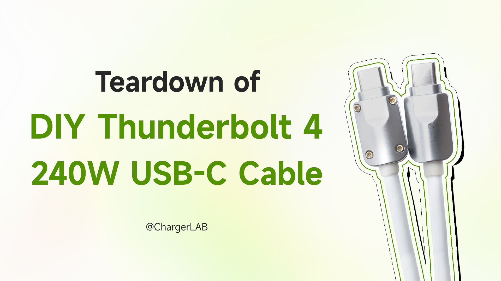
Chargerlab Chargerlab
  • News
    • What's New
    • Interviews
    • Vlogs
    • Events
    • Industry
  • Reviews
    • Charging Compatibility
    • Fully Charging
    • Comparison
    • Chargers & Cables
    • Power Banks & Stations
    • Mobile Devices
    • Accessories
  • Teardowns
    • Chargers & Cables
    • Power Banks & Stations
    • Power Supplies
    • Prototypes
    • Batteries
    • Accessories
  • Videos
    • YouTube
    • TikTok
  • Guides
    • How to Buy
    • Explained
    • Deals
    • ICs
  • POWER-Z
    • KM003C/KM002C
    • KT002
    • Buy POWER-Z
    • Technical Support
  • Contact Us
Home › Teardowns › Chargers & Cables › Teardown of ASUS ROG 130W USB-C GaN Power Adapter (ADP-130HB B)
  • 1

Teardown of ASUS ROG 130W USB-C GaN Power Adapter (ADP-130HB B)

Rusell
November 11, 2024

Introduction

ChargerLAB this time got a 130W USB-C power adapter from ROG. The input end of this adapter uses a three-prong design and supports a wide input voltage of 100-240V. It also comes with a USB-C output cable. It has passed multiple safety certifications. Next, let's take it apart to see its internal components and structure.

Product Appearance

Teardown of ASUS ROG 130W USB-C GaN Power Adapter (ADP-130HB B)-Chargerlab

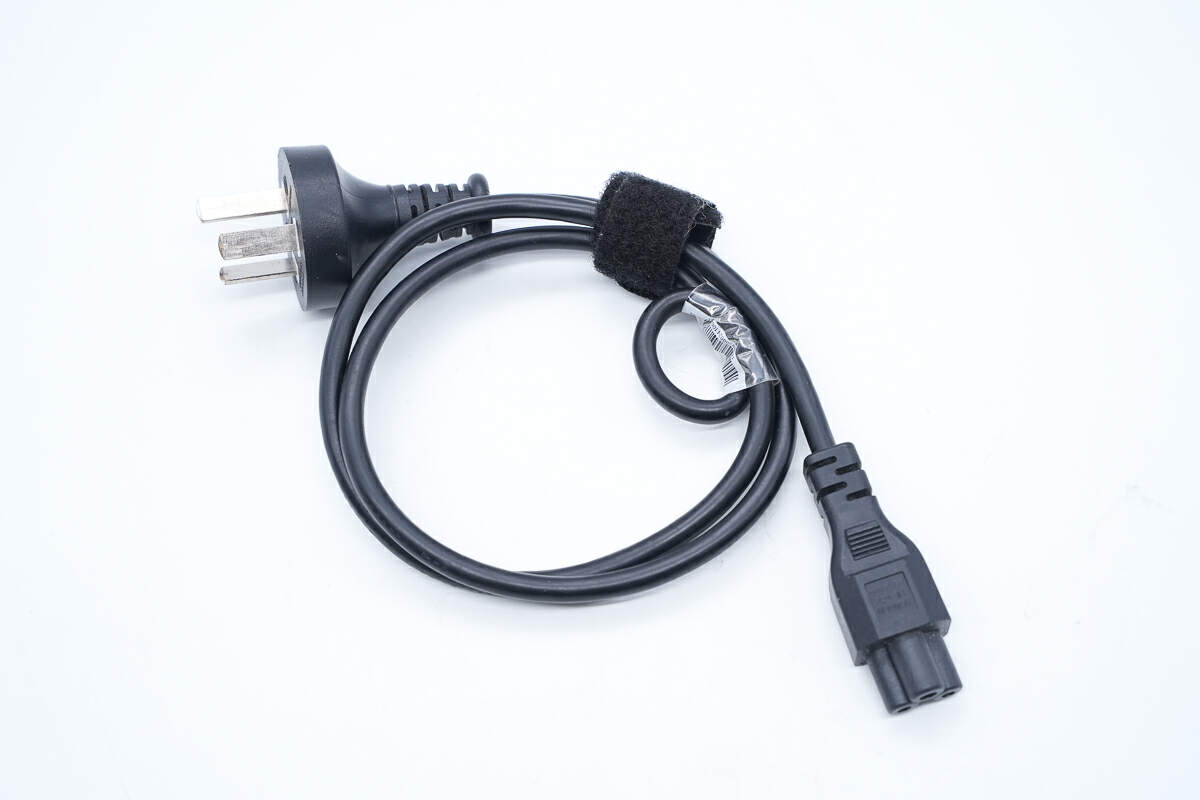
The power cord of the ASUS ROG 130W USB-C GaN Power Adapter is detachable, allowing users to replace different power cords for use in different countries and regions.

Teardown of ASUS ROG 130W USB-C GaN Power Adapter (ADP-130HB B)-Chargerlab

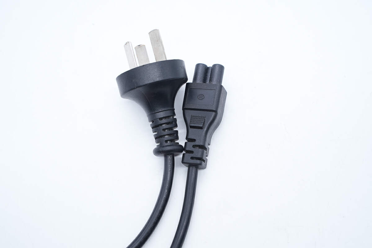
Both sides of the power cord adopt the three-prong design.

Teardown of ASUS ROG 130W USB-C GaN Power Adapter (ADP-130HB B)-Chargerlab

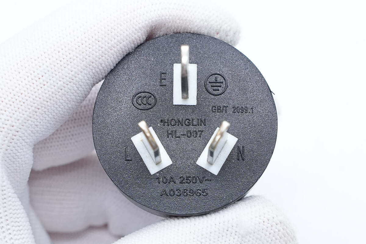
It can support input of 10A 250V~.

Teardown of ASUS ROG 130W USB-C GaN Power Adapter (ADP-130HB B)-Chargerlab

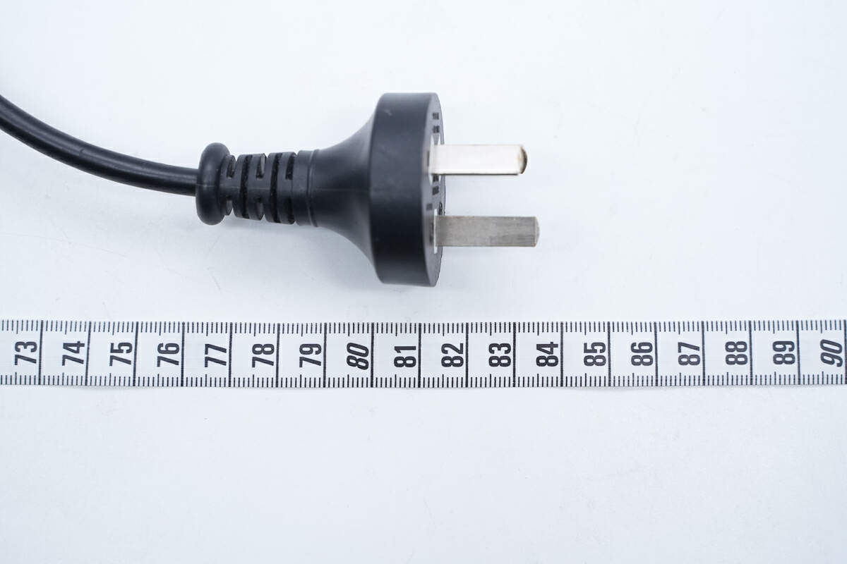
The total length of the power cord is about 83.5 cm (32.87 inches).

Teardown of ASUS ROG 130W USB-C GaN Power Adapter (ADP-130HB B)-Chargerlab

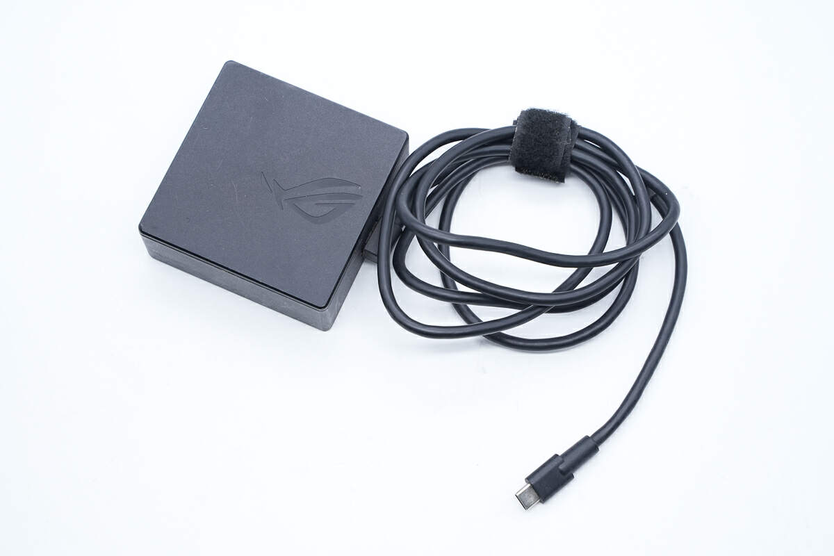
The power adapter is in the shape of a flat rectangle and comes with a USB-C output cable.

Teardown of ASUS ROG 130W USB-C GaN Power Adapter (ADP-130HB B)-Chargerlab

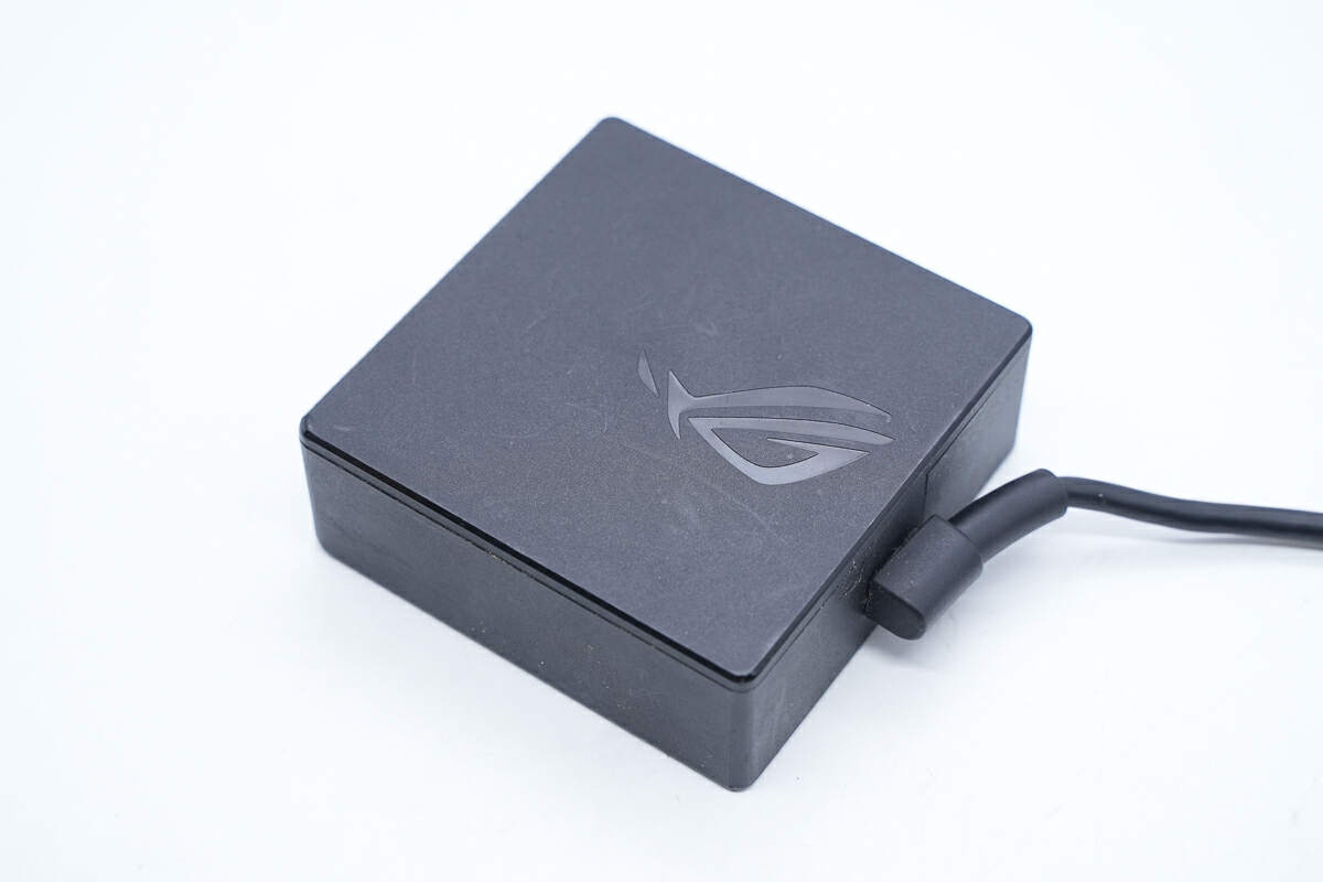
The black case is made of fire-retardant PC material, and the surface has a matte design.

Teardown of ASUS ROG 130W USB-C GaN Power Adapter (ADP-130HB B)-Chargerlab

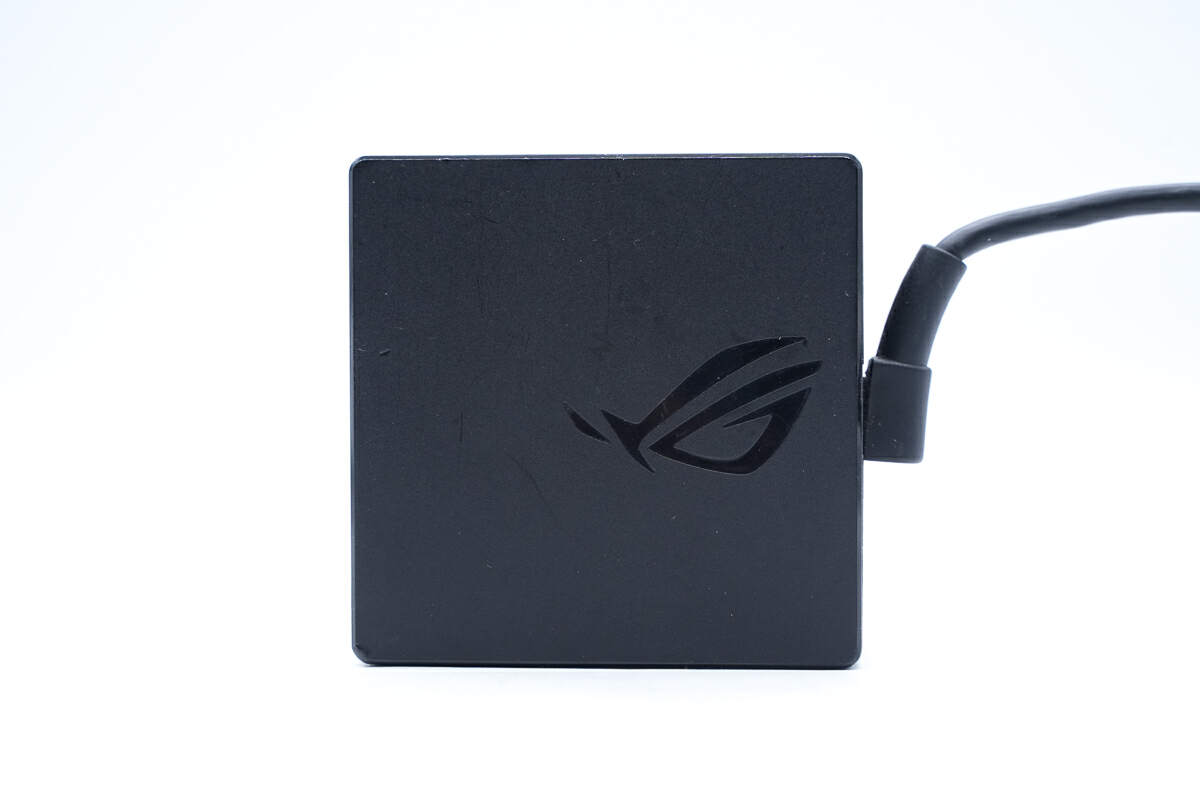
There is a glossy ROG logo printed on the front.

Teardown of ASUS ROG 130W USB-C GaN Power Adapter (ADP-130HB B)-Chargerlab

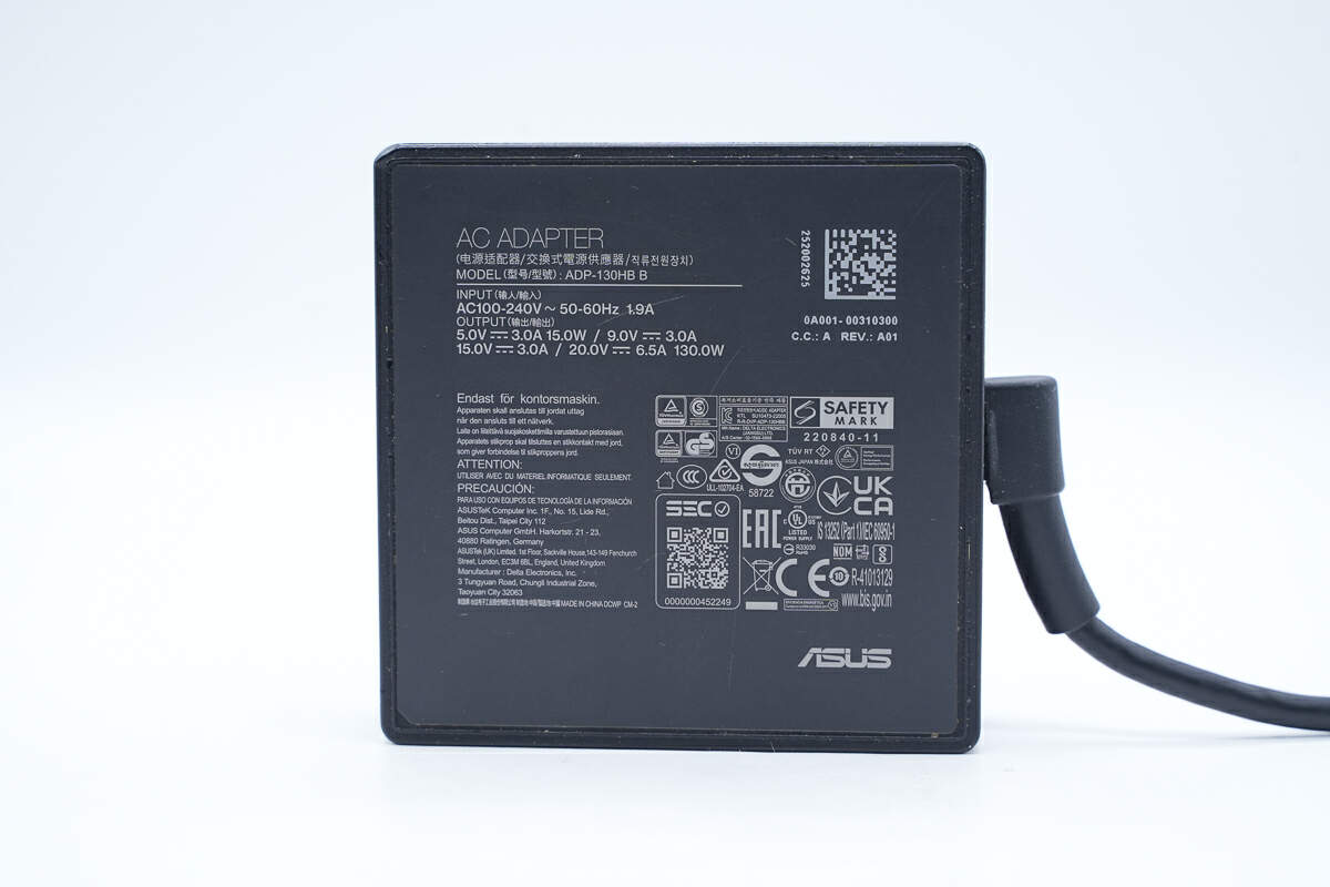
There is a piece of anti-slip rubber pad on the bottom, and the specs info is printed on it. It has passed multiple safety certifications such as CCC, CE, GS, EAC, UKCA, UL, NOM, NYCE, etc., and can be used in most countries and regions.

Teardown of ASUS ROG 130W USB-C GaN Power Adapter (ADP-130HB B)-Chargerlab

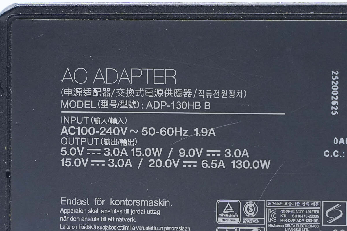
Model is ADP-130HB B. It can support input of 100-240V~50/60Hz 1.9A. The maximum output is 20V 6.5A, which is 130W. The manufacturer is Delta.

Teardown of ASUS ROG 130W USB-C GaN Power Adapter (ADP-130HB B)-Chargerlab

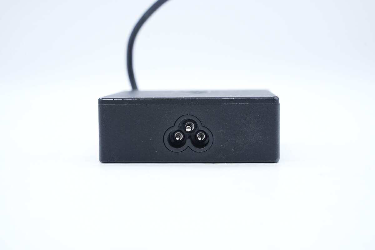
The input end has a three-prong slot.

Teardown of ASUS ROG 130W USB-C GaN Power Adapter (ADP-130HB B)-Chargerlab

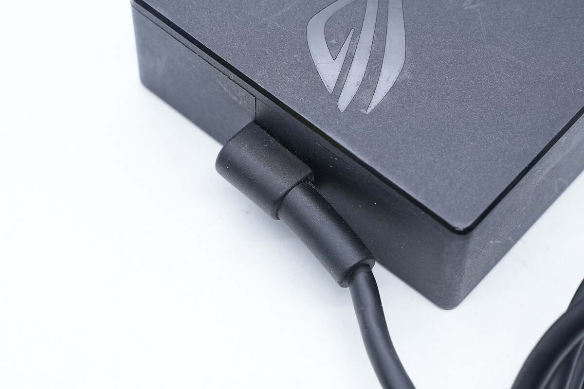
The connection between the output cable and the adapter adopts a bent design, which can save space and protect the cable.

Teardown of ASUS ROG 130W USB-C GaN Power Adapter (ADP-130HB B)-Chargerlab

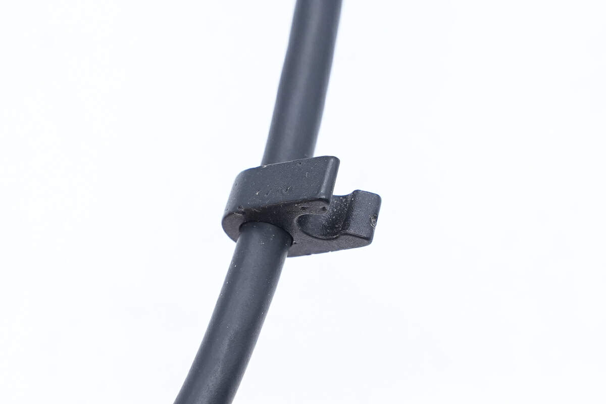
There is a cable clip on the output cable.

Teardown of ASUS ROG 130W USB-C GaN Power Adapter (ADP-130HB B)-Chargerlab

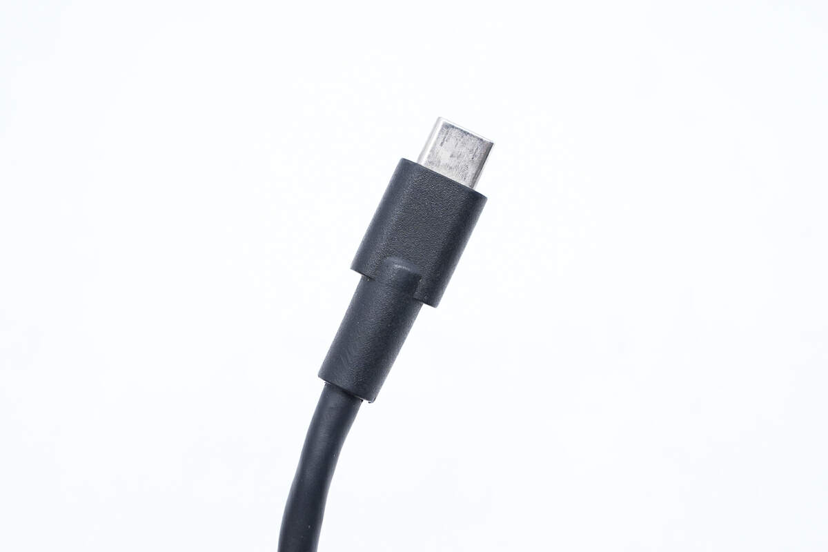
The USB-C connector adopts a thickened design.

Teardown of ASUS ROG 130W USB-C GaN Power Adapter (ADP-130HB B)-Chargerlab

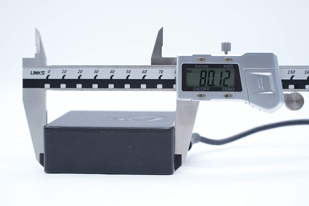
The length of the power adapter is about 80 mm (3.15 inches).

Teardown of ASUS ROG 130W USB-C GaN Power Adapter (ADP-130HB B)-Chargerlab

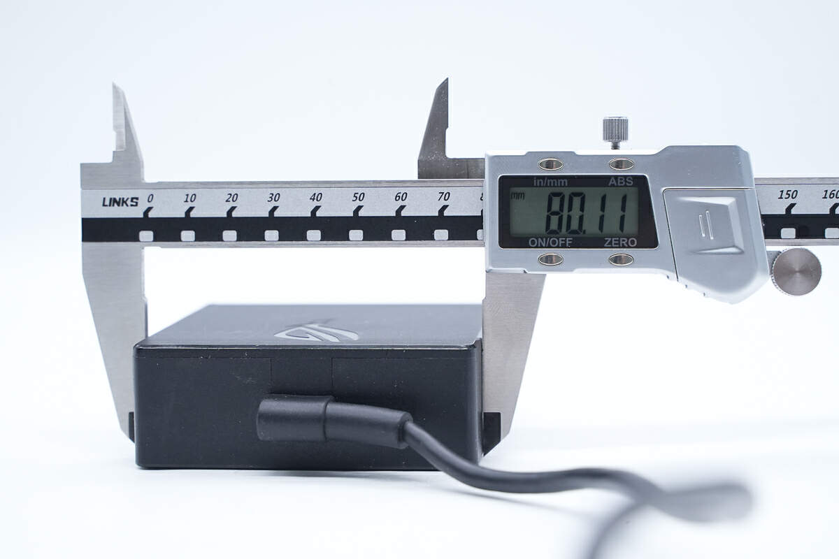
The width is also about 80 mm (3.15 inches).

Teardown of ASUS ROG 130W USB-C GaN Power Adapter (ADP-130HB B)-Chargerlab

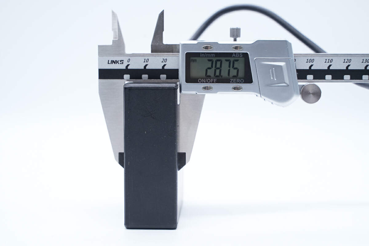
And the thickness is about 28.8 mm (1.13 inches).

Teardown of ASUS ROG 130W USB-C GaN Power Adapter (ADP-130HB B)-Chargerlab

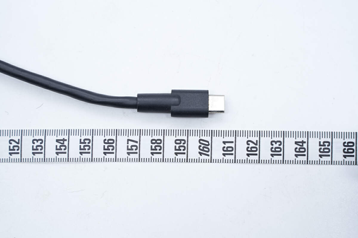
The length of the USB-C cable is about 160.5 cm (63.19 inches).

Teardown of ASUS ROG 130W USB-C GaN Power Adapter (ADP-130HB B)-Chargerlab

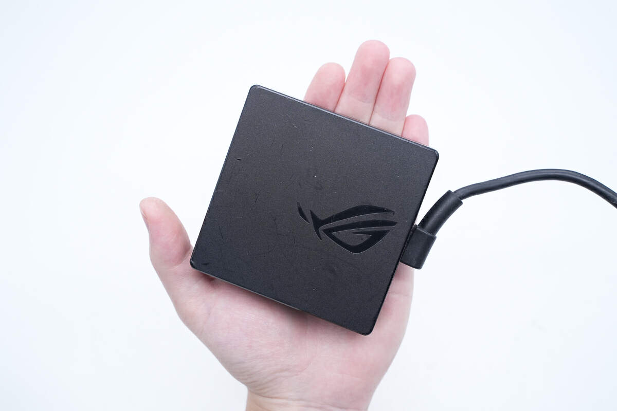
That's how big it is in the hand.

Teardown of ASUS ROG 130W USB-C GaN Power Adapter (ADP-130HB B)-Chargerlab

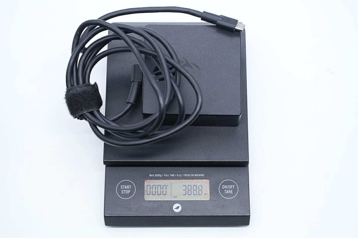
The weight is about 389 g (13.72 oz).

Teardown of ASUS ROG 130W USB-C GaN Power Adapter (ADP-130HB B)-Chargerlab

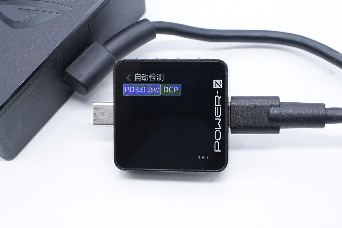
ChargerLAB POWER-Z KM003C shows the USB-C port can support PD3.0 and DCP charging protocols.

Teardown of ASUS ROG 130W USB-C GaN Power Adapter (ADP-130HB B)-Chargerlab

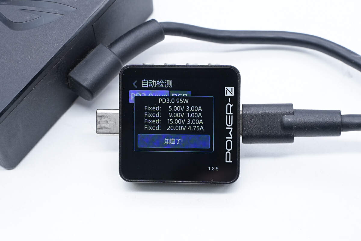
And it has four fixed PDOs of 5V3A, 9V3A, 15V3A, and 20V4.75A.

Teardown

Teardown of ASUS ROG 130W USB-C GaN Power Adapter (ADP-130HB B)-Chargerlab

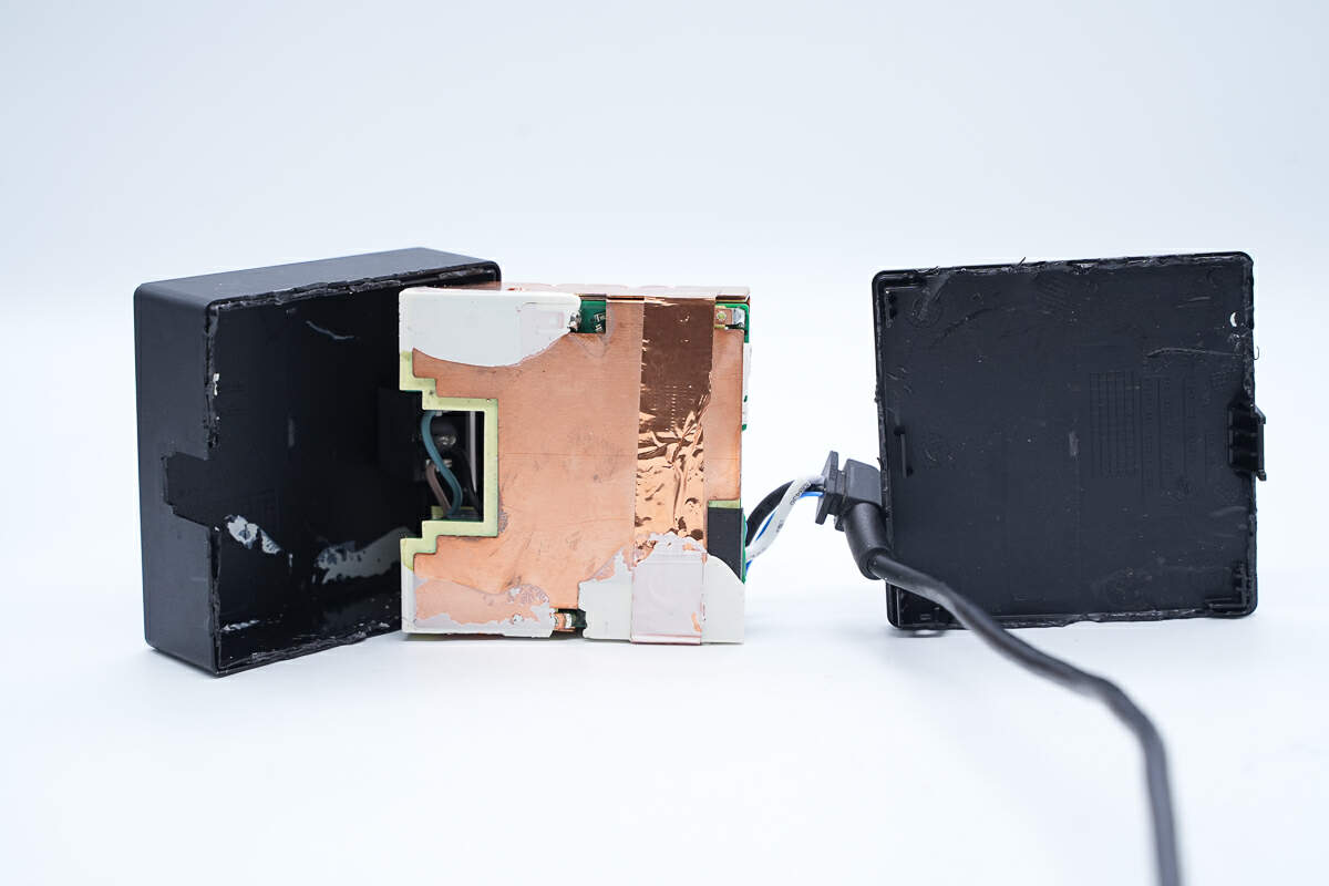
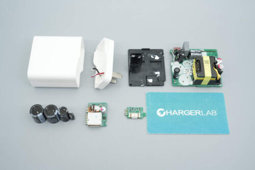
First, pry off the bottom shell along the gap, which uses an ultrasonic welding process. 

Teardown of ASUS ROG 130W USB-C GaN Power Adapter (ADP-130HB B)-Chargerlab

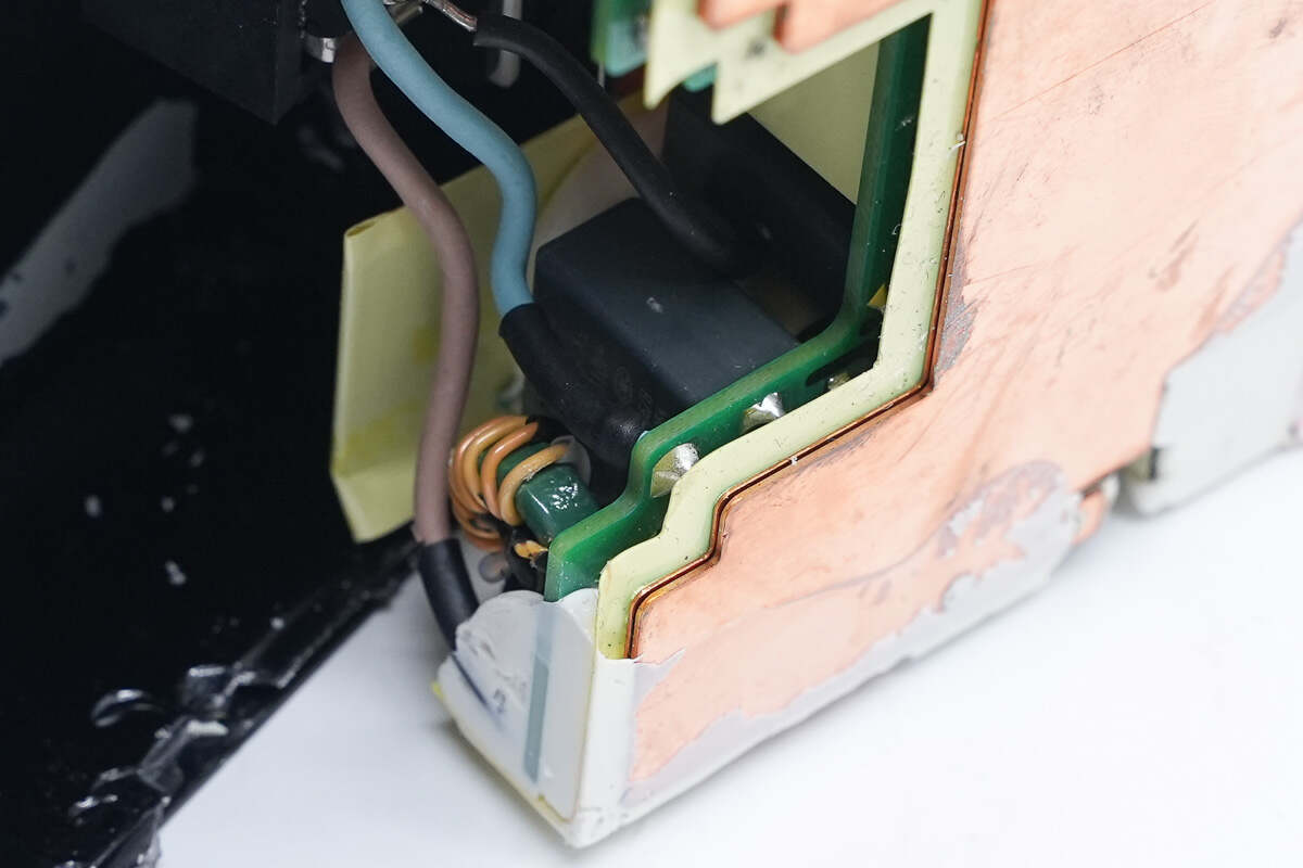
The input socket is connected to the PCBA module through wires and protected by rubber sleeves.

Teardown of ASUS ROG 130W USB-C GaN Power Adapter (ADP-130HB B)-Chargerlab

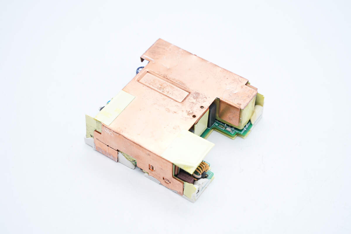
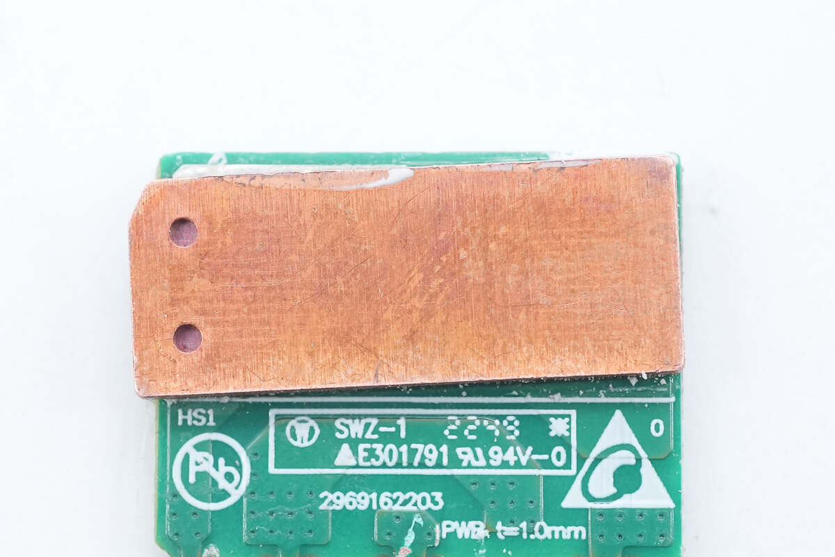
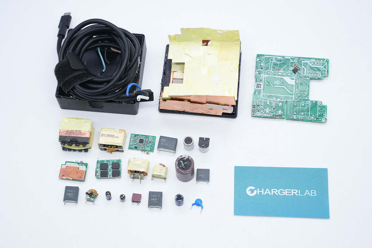
Take out the PCBA module. The entire module is covered with copper sheets for heat dissipation, and tape is pasted on the inside, and both ends for insulation.

Teardown of ASUS ROG 130W USB-C GaN Power Adapter (ADP-130HB B)-Chargerlab

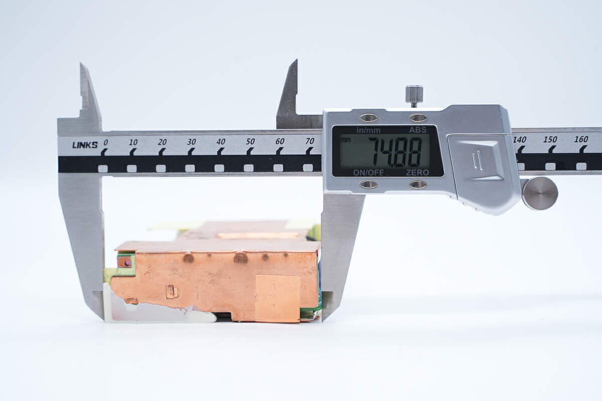
The length of the PCBA module is 74.88 mm (2.95 inches).

Teardown of ASUS ROG 130W USB-C GaN Power Adapter (ADP-130HB B)-Chargerlab

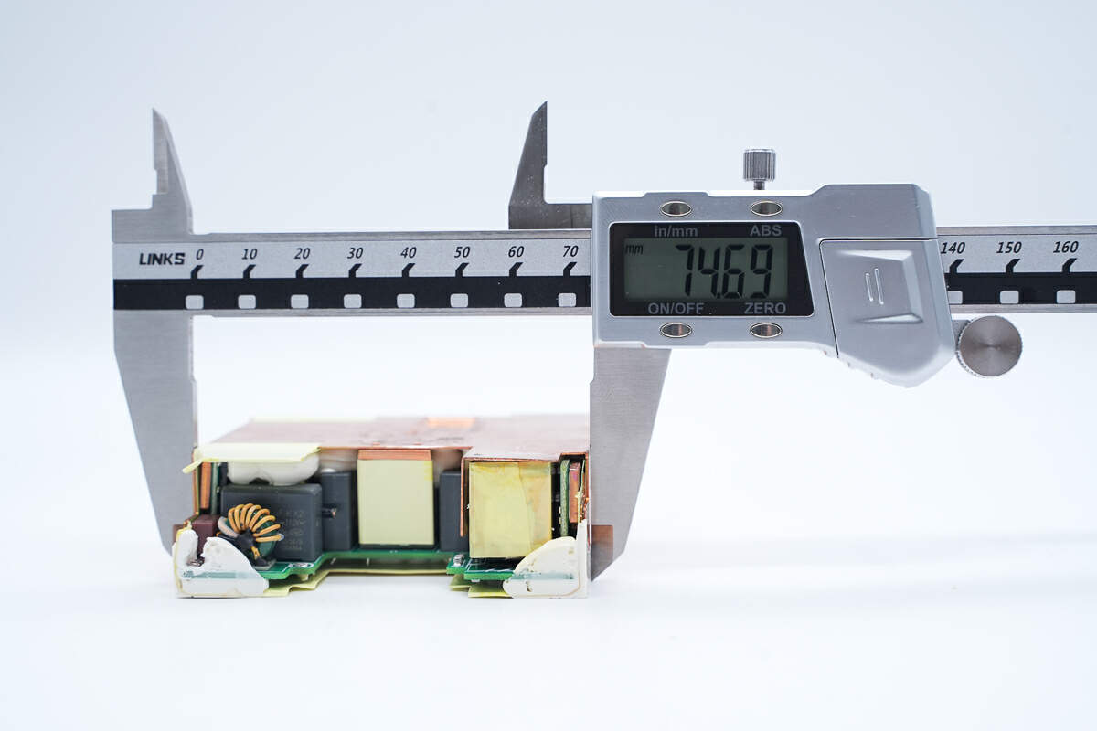
The width is 74.69 mm (2.94 inches).

Teardown of ASUS ROG 130W USB-C GaN Power Adapter (ADP-130HB B)-Chargerlab

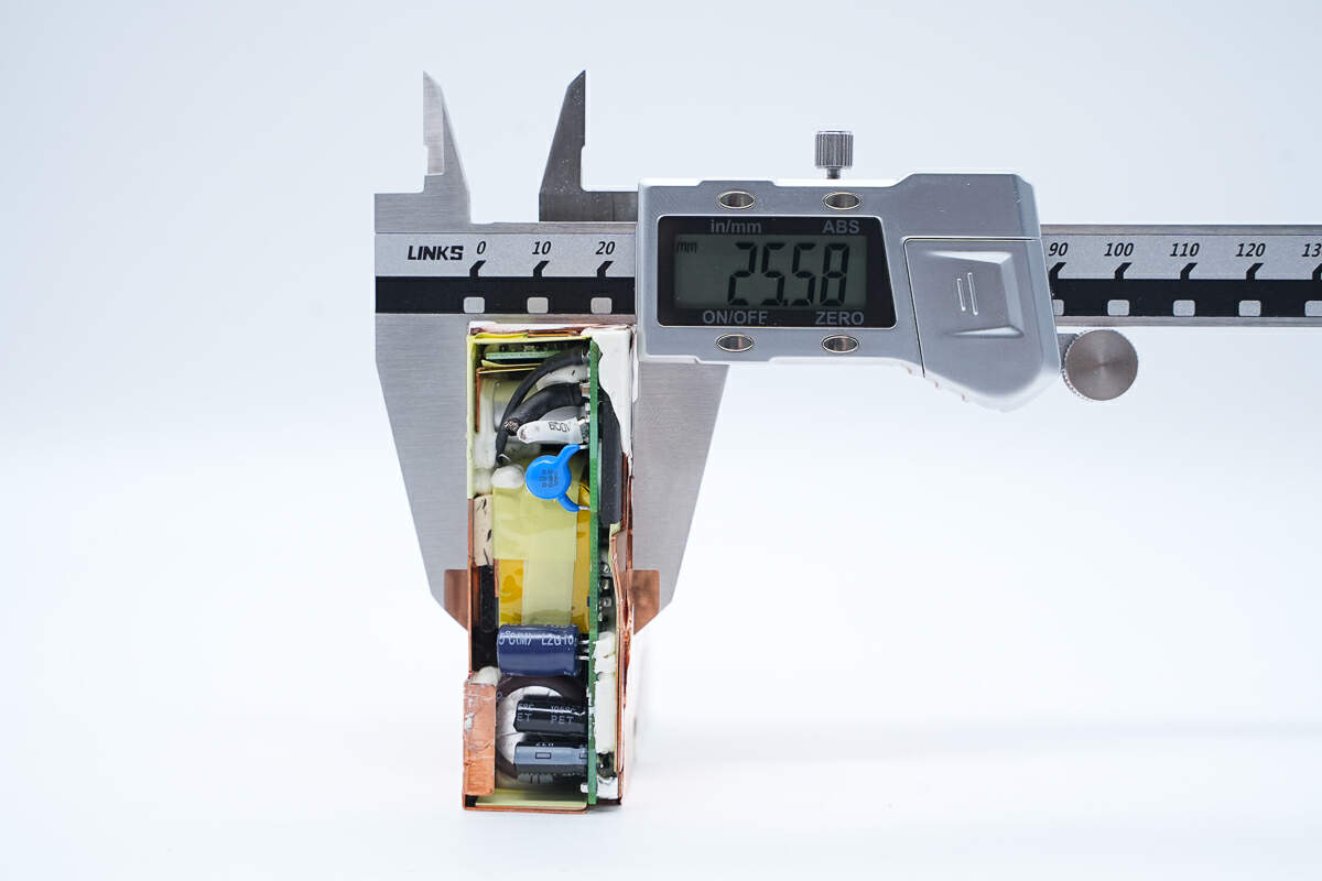
And the thickness is about 25.58 mm (1.0071 inches).

Teardown of ASUS ROG 130W USB-C GaN Power Adapter (ADP-130HB B)-Chargerlab

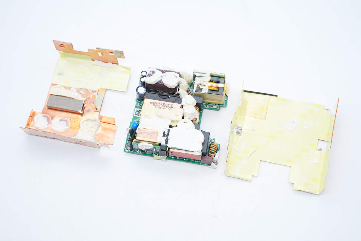
Remove the heat sink, and the conductive cloth is pasted on the corresponding position of the transformer.

Teardown of ASUS ROG 130W USB-C GaN Power Adapter (ADP-130HB B)-Chargerlab

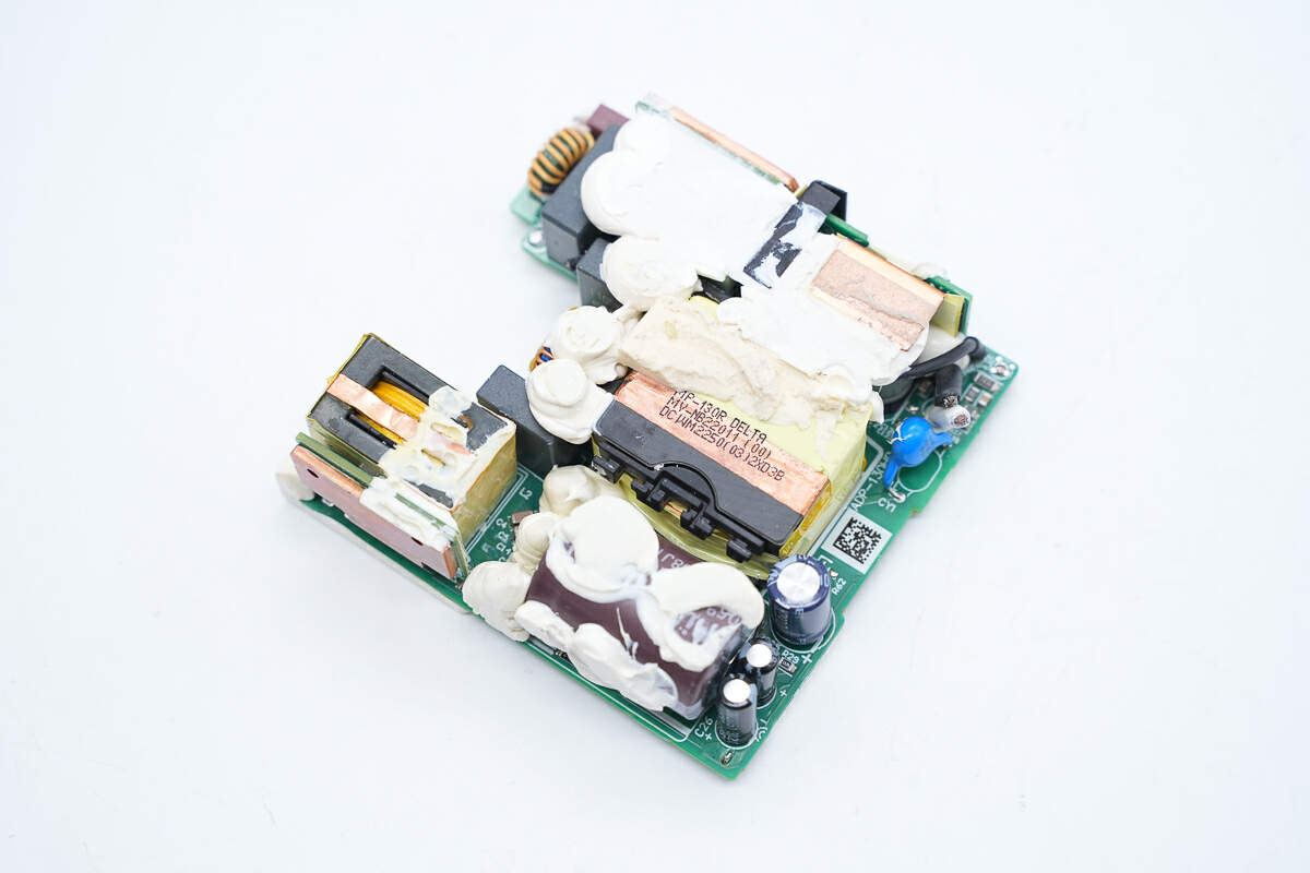
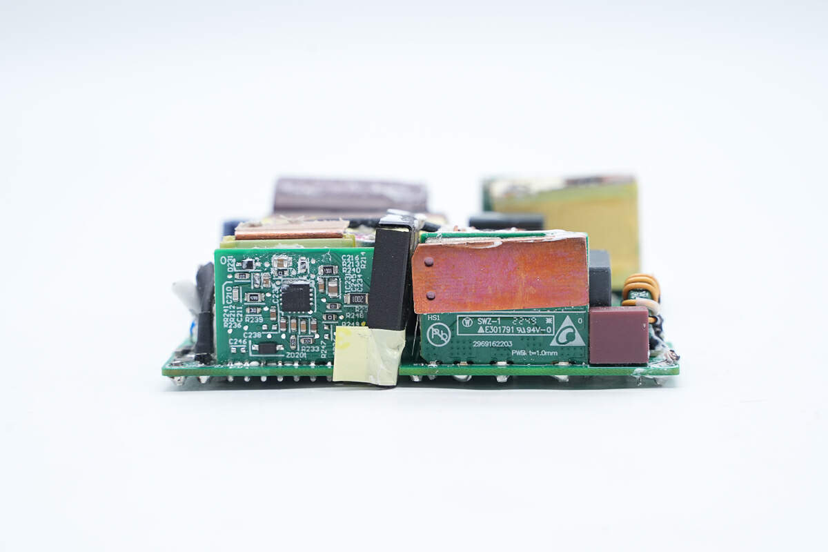
The components on the front of the PCBA module are filled with potting compound, and there are two small heat-dissipation copper sheets on both sides.

Teardown of ASUS ROG 130W USB-C GaN Power Adapter (ADP-130HB B)-Chargerlab

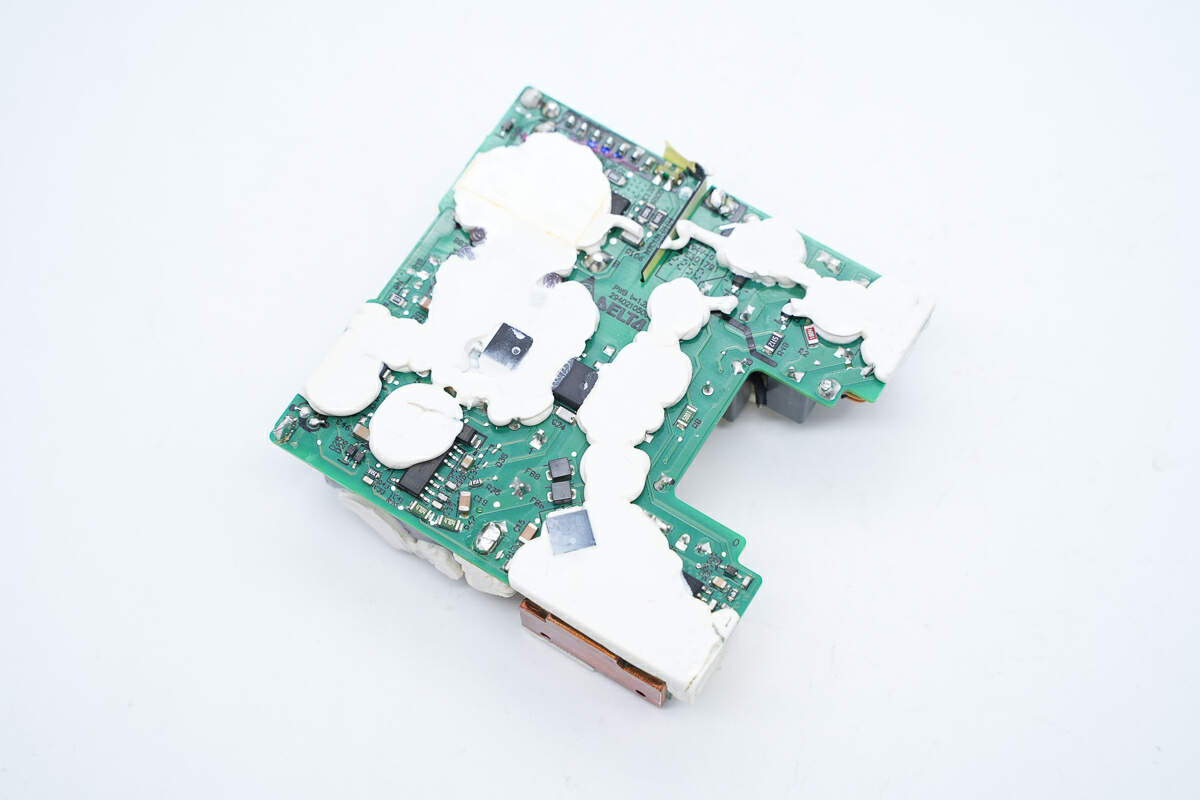
The main components on the back of the PCBA module also use the potting compound to help dissipate heat.

Teardown of ASUS ROG 130W USB-C GaN Power Adapter (ADP-130HB B)-Chargerlab

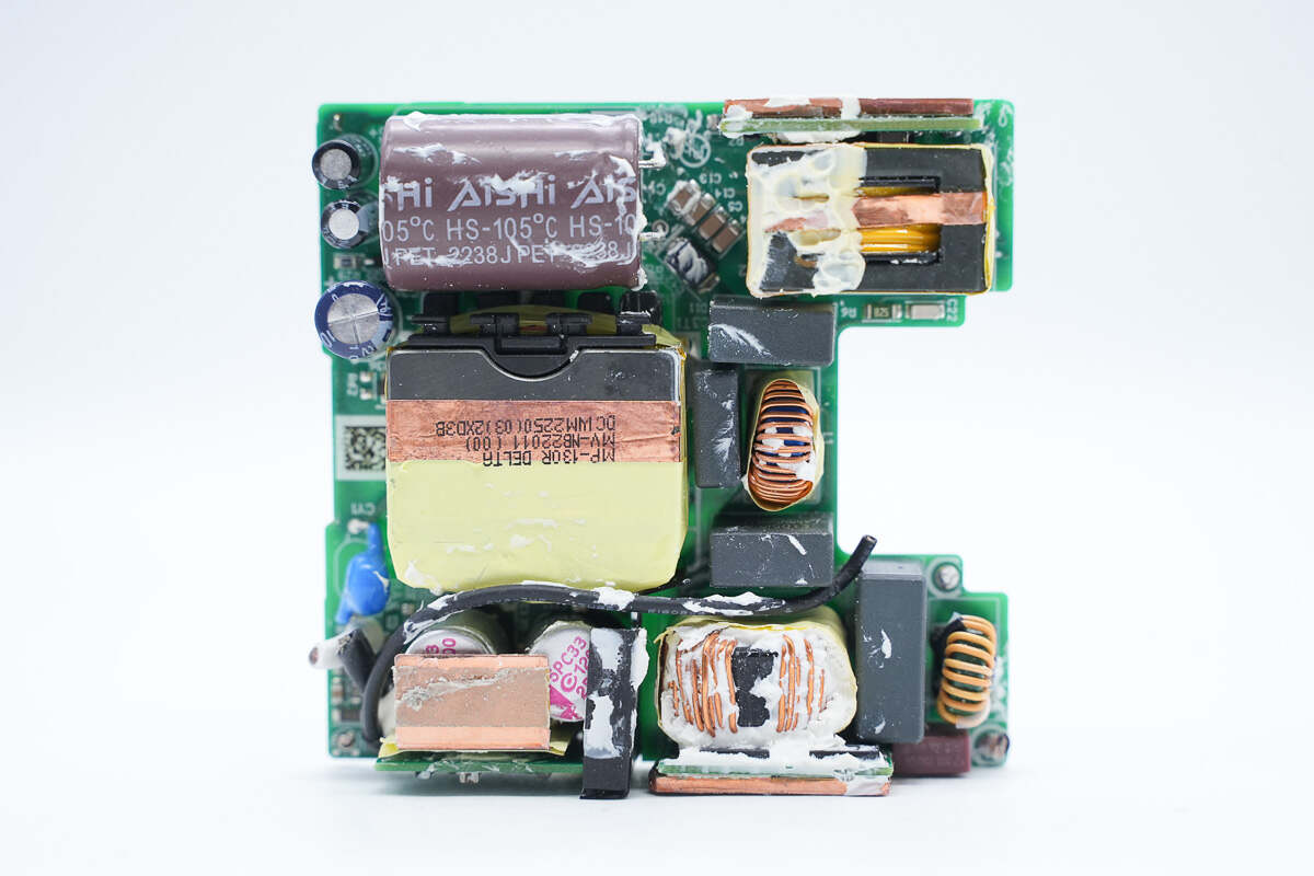
Clean up the potting compound. The time delay fuse, common mode choke, film capacitor, filter inductor, PFC boost inductor, electrolytic capacitor, transformer, and other components are on the front of the PCBA module.

Teardown of ASUS ROG 130W USB-C GaN Power Adapter (ADP-130HB B)-Chargerlab

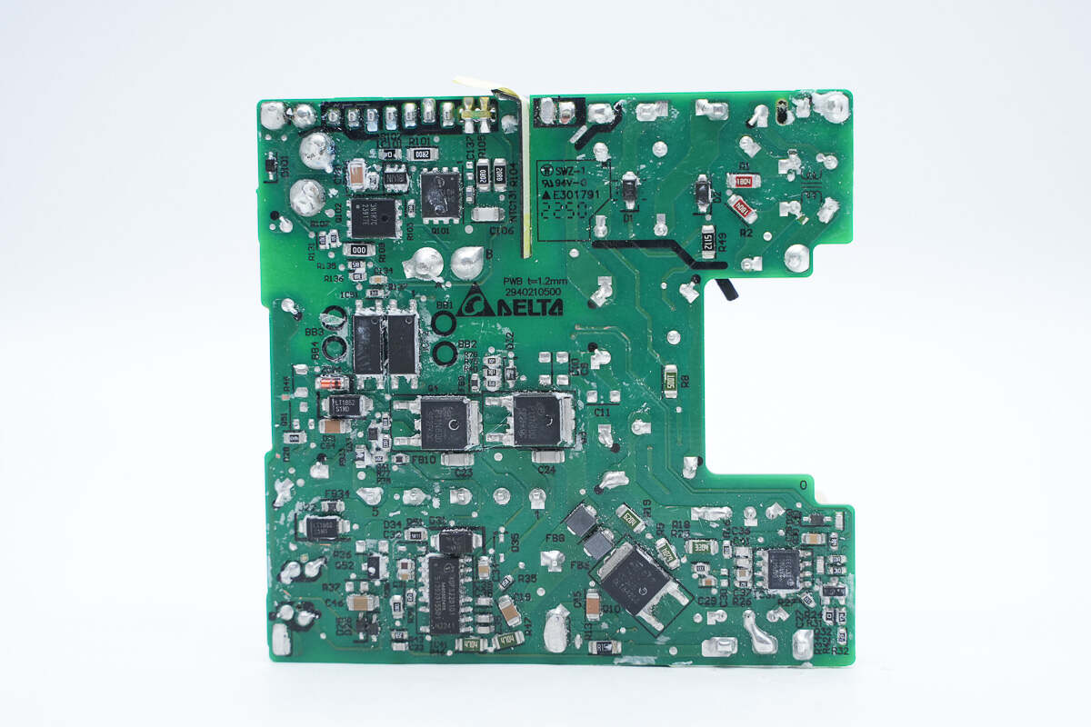
There is PFC controller, PFC rectifier, master control chip, HFB half-bridge MOSFET, optocoupler, synchronous rectifier controller, and synchronous rectifier on the back of the PCBA module.

Teardown of ASUS ROG 130W USB-C GaN Power Adapter (ADP-130HB B)-Chargerlab

On the left side of the input end, there is a time delay fuse, common mode choke, and safety X capacitor, and the filter inductor in the middle is wrapped with tape for insulation.

Teardown of ASUS ROG 130W USB-C GaN Power Adapter (ADP-130HB B)-Chargerlab

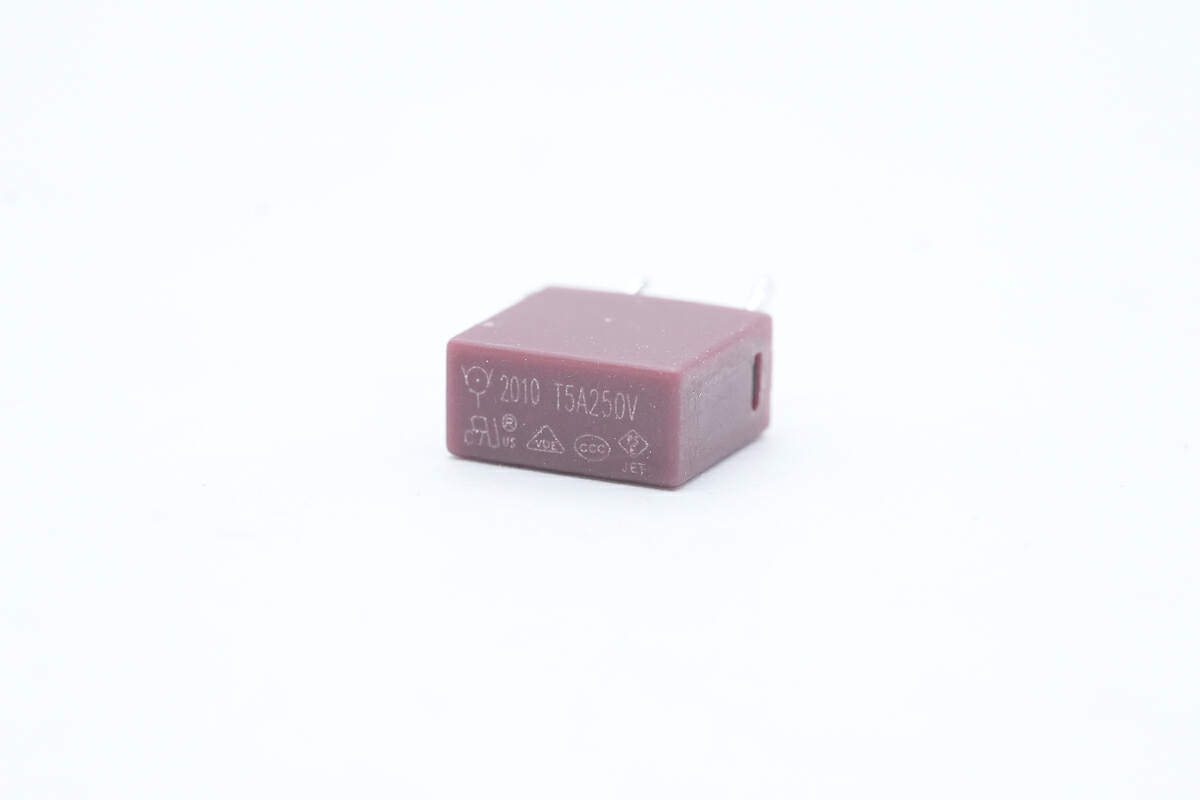
The time delay fuse is from WalterFuse. 5A 250V.

Teardown of ASUS ROG 130W USB-C GaN Power Adapter (ADP-130HB B)-Chargerlab

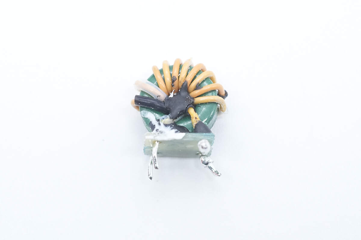
There is the common mode choke.

Teardown of ASUS ROG 130W USB-C GaN Power Adapter (ADP-130HB B)-Chargerlab

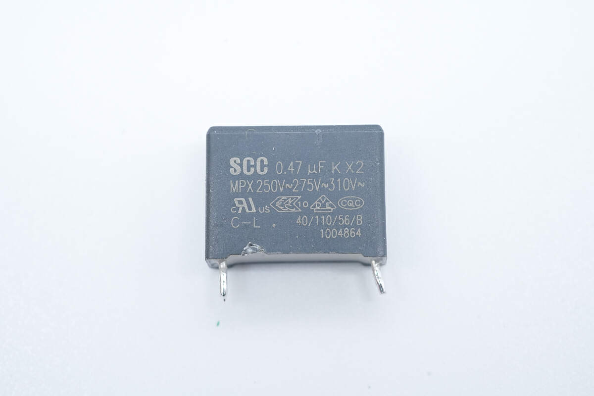
The safety X2 capacitor is from SCC. 0.47μF.

Teardown of ASUS ROG 130W USB-C GaN Power Adapter (ADP-130HB B)-Chargerlab

The common mode choke is insulated by tape.

Teardown of ASUS ROG 130W USB-C GaN Power Adapter (ADP-130HB B)-Chargerlab

There is a mylar sheet between the PCB of the bridge rectifier and the PCB of the output protocol for isolation protection.

Teardown of ASUS ROG 130W USB-C GaN Power Adapter (ADP-130HB B)-Chargerlab

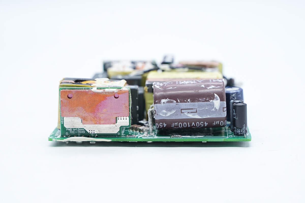
Remove the PCB of the bridge rectifier, and there is a copper heat sink on the back.

Teardown of ASUS ROG 130W USB-C GaN Power Adapter (ADP-130HB B)-Chargerlab

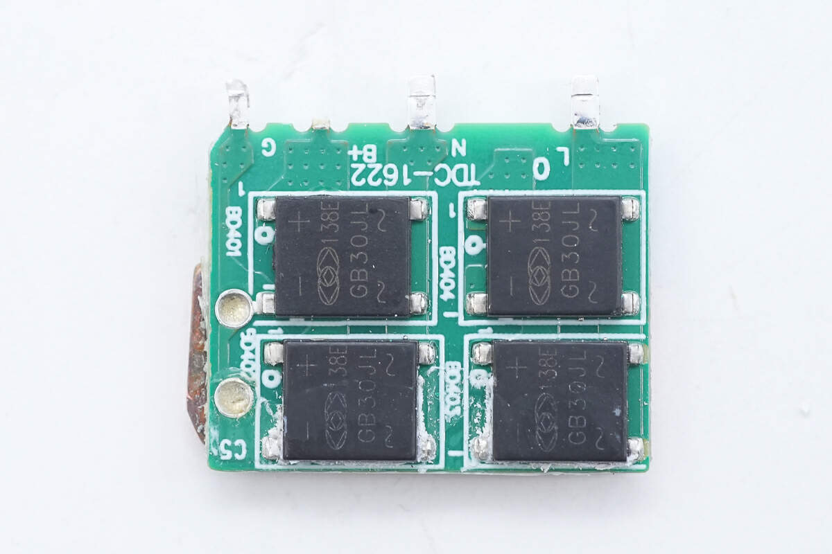
There are four bridge rectifiers on the front. The models are all GB30JL.

Teardown of ASUS ROG 130W USB-C GaN Power Adapter (ADP-130HB B)-Chargerlab

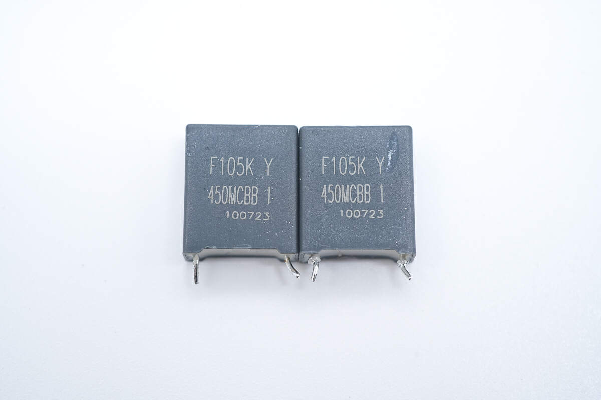
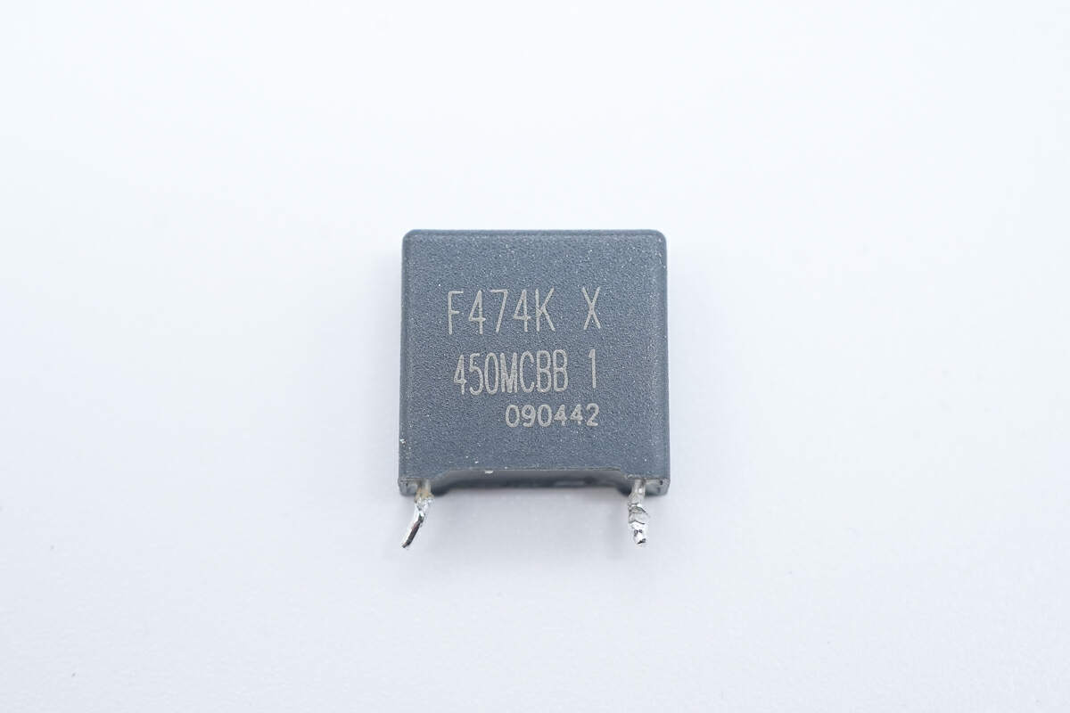
These are two film capacitors. 1μF 450V.

Teardown of ASUS ROG 130W USB-C GaN Power Adapter (ADP-130HB B)-Chargerlab

The filter inductor is insulated by tape.

Teardown of ASUS ROG 130W USB-C GaN Power Adapter (ADP-130HB B)-Chargerlab

There is a PCB of the PFC boost circuit next to the PFC boost inductor and an electrolytic capacitor on the right.

Teardown of ASUS ROG 130W USB-C GaN Power Adapter (ADP-130HB B)-Chargerlab

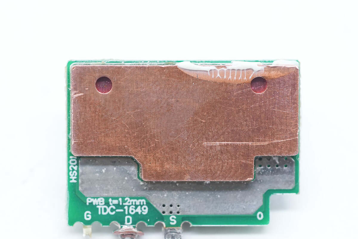
There is a copper heat sink on the back.

Teardown of ASUS ROG 130W USB-C GaN Power Adapter (ADP-130HB B)-Chargerlab

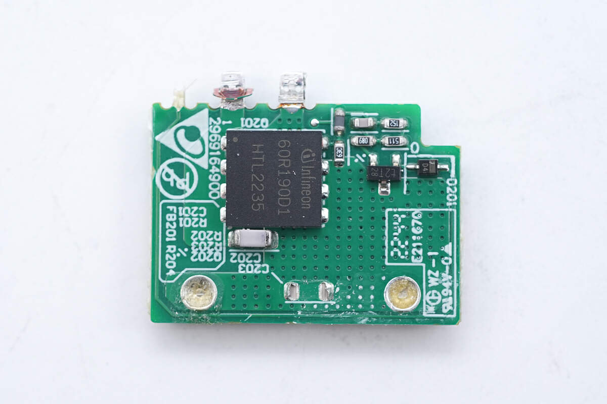
There is a PFC MOSFET on the front.

Teardown of ASUS ROG 130W USB-C GaN Power Adapter (ADP-130HB B)-Chargerlab

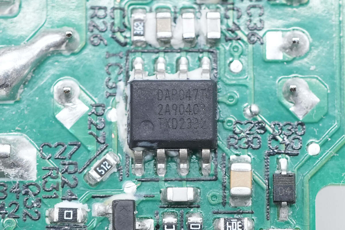
The PFC controller marked with DAP047T is from Delta.

Teardown of ASUS ROG 130W USB-C GaN Power Adapter (ADP-130HB B)-Chargerlab

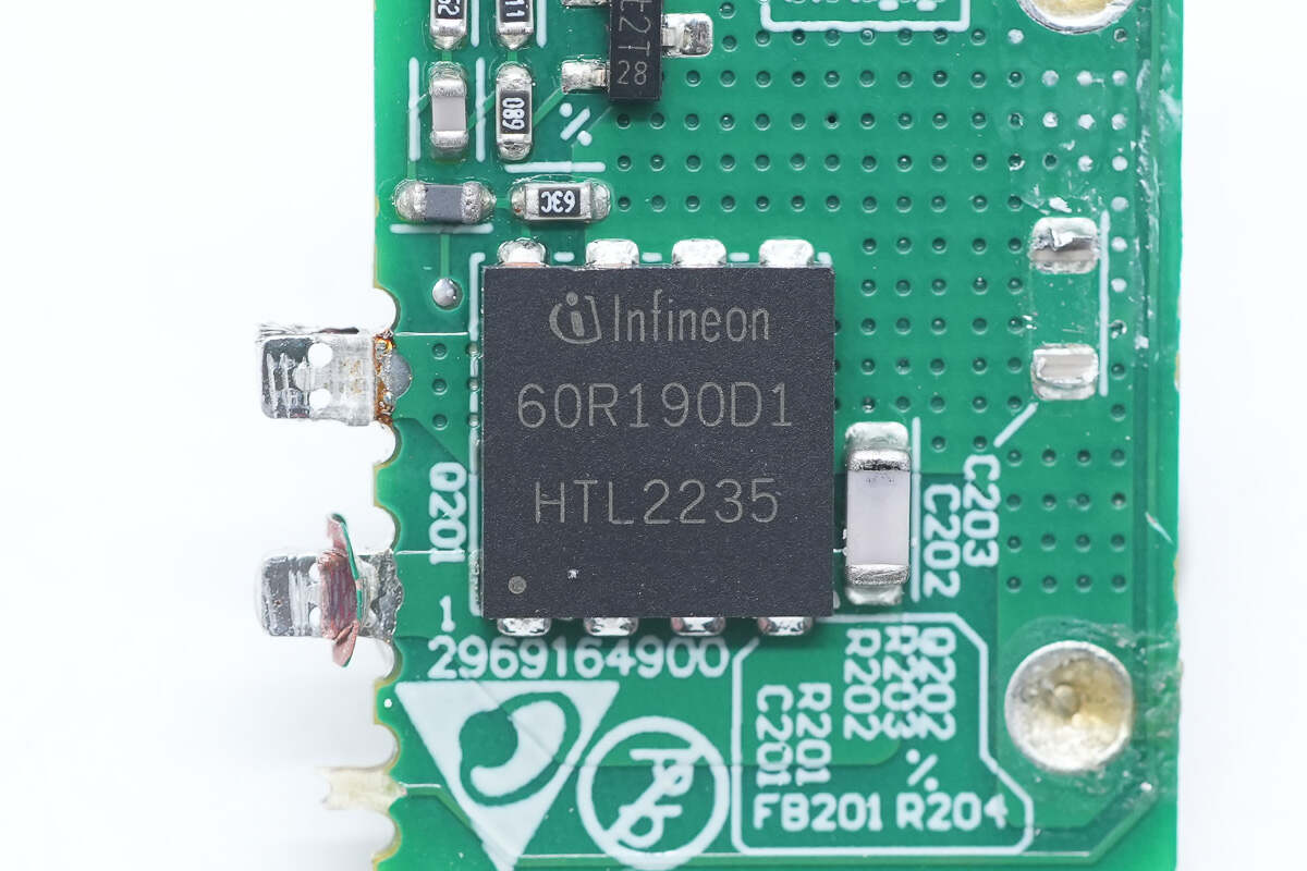
The PFC MOSFET is from Infineon and adopts PG-LSON-8-1 package. The withstand voltage is 600V, and the resistance is 140mΩ. Model is IGLD60R190D1.

Teardown of ASUS ROG 130W USB-C GaN Power Adapter (ADP-130HB B)-Chargerlab

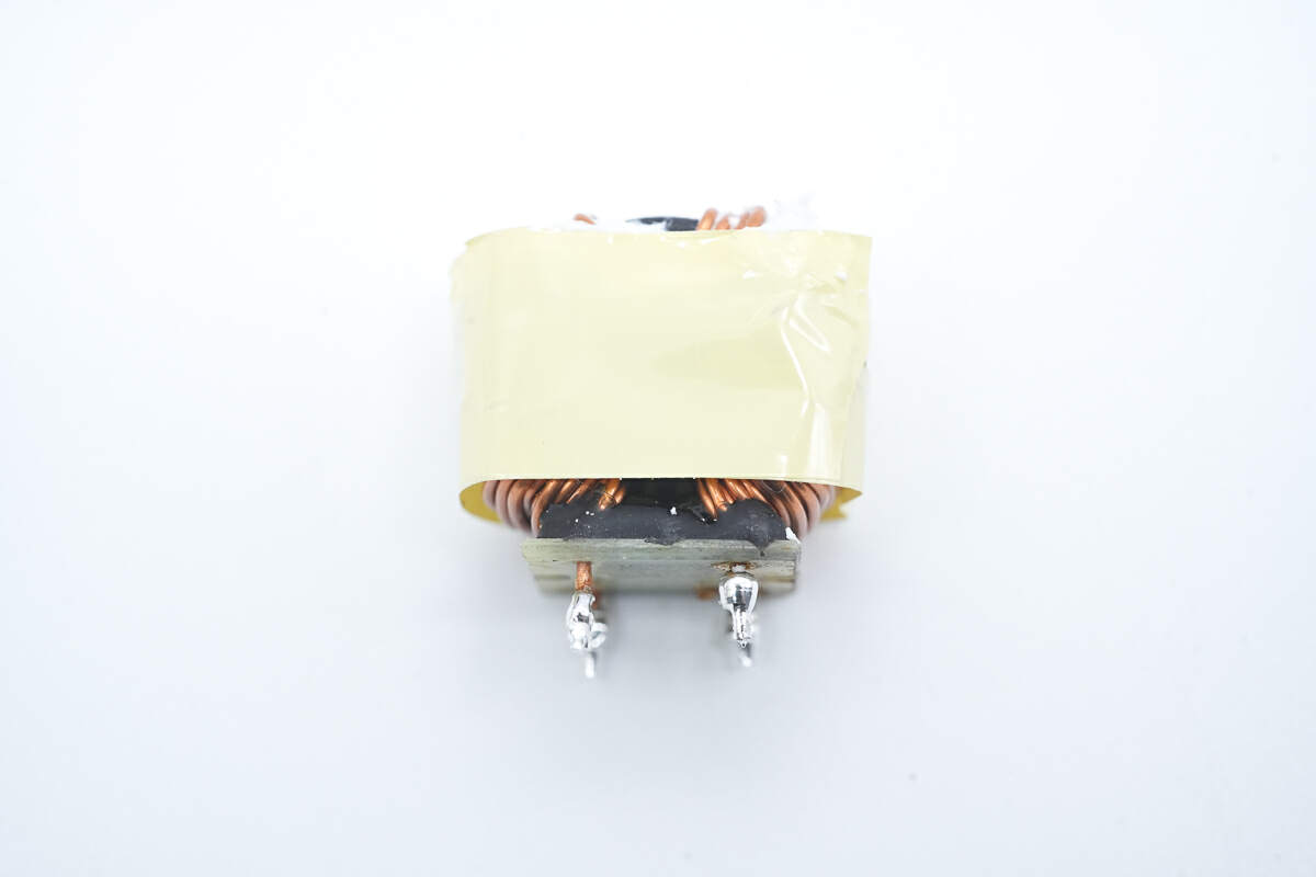
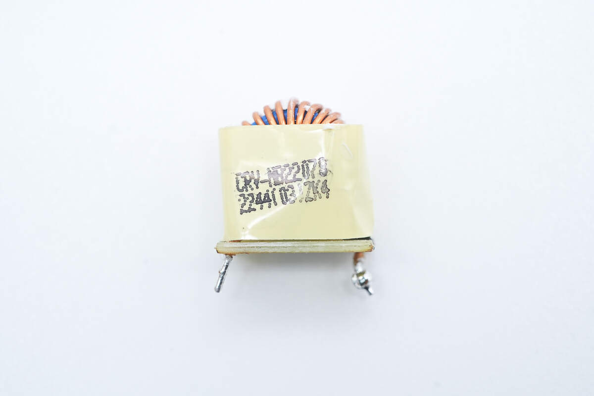
Here is the PFC boost inductor.

Teardown of ASUS ROG 130W USB-C GaN Power Adapter (ADP-130HB B)-Chargerlab

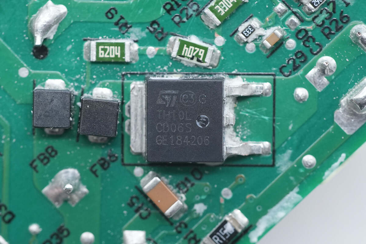
The PFC rectifier is from ST and adopts DPAK package. Model is STTH10LCD06S. 10A 600V.

Teardown of ASUS ROG 130W USB-C GaN Power Adapter (ADP-130HB B)-Chargerlab

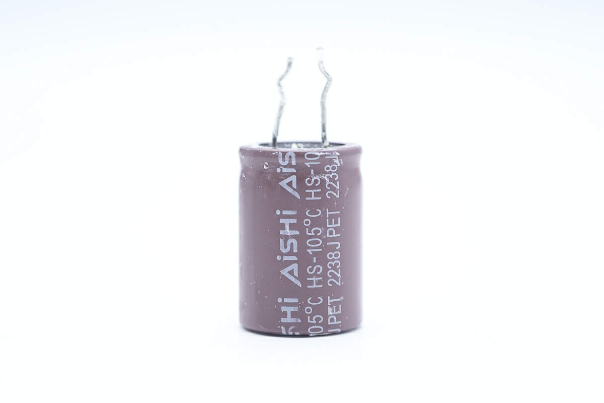
The electrolytic capacitor is from AiSHi. 450V 100μF.

Teardown of ASUS ROG 130W USB-C GaN Power Adapter (ADP-130HB B)-Chargerlab

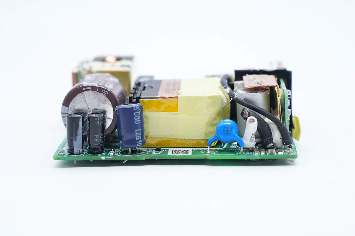
On the left side of the output end, there are capacitors that power the master control chip, in the middle is the transformer, and on the right side is the Y capacitor and the solid capacitor for output filtering.

Teardown of ASUS ROG 130W USB-C GaN Power Adapter (ADP-130HB B)-Chargerlab

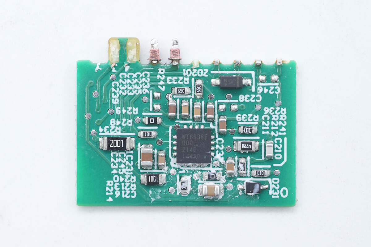
Remove the output PCB, and there is a protocol chip.

Teardown of ASUS ROG 130W USB-C GaN Power Adapter (ADP-130HB B)-Chargerlab

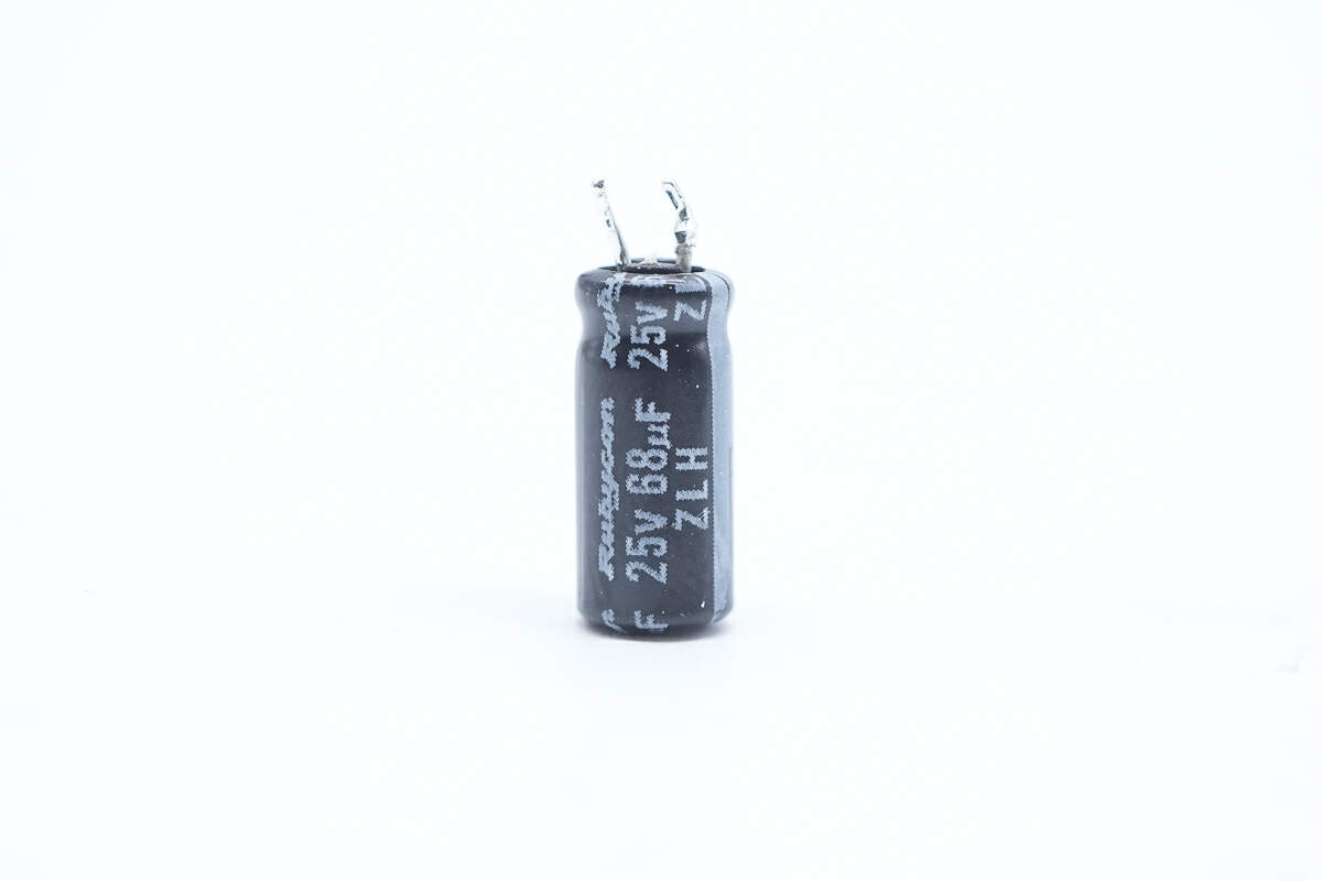
The capacitors that power the master control chip are from Rubycon. 25V 68μF.

Teardown of ASUS ROG 130W USB-C GaN Power Adapter (ADP-130HB B)-Chargerlab

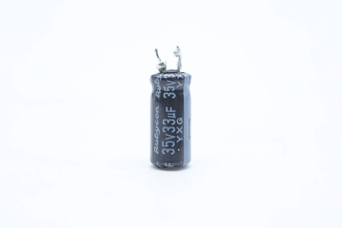
The other one is also from Rubycon. 35V 33μF.

Teardown of ASUS ROG 130W USB-C GaN Power Adapter (ADP-130HB B)-Chargerlab

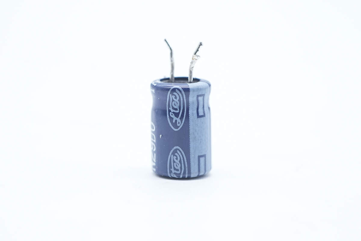
Another one is from LTEC. 100V 22μF.

Teardown of ASUS ROG 130W USB-C GaN Power Adapter (ADP-130HB B)-Chargerlab

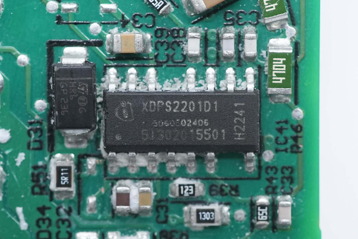
The master control chip is from Infineon and adopts PG-DSO-14 package. It is a digital hybrid flyback controller with an integrated 600V high-voltage startup circuit and high- and low-side MOS drivers. It supports primary side overvoltage protection, and standby power consumption is less than 75mW. Model is XPDS2201. 

Teardown of ASUS ROG 130W USB-C GaN Power Adapter (ADP-130HB B)-Chargerlab

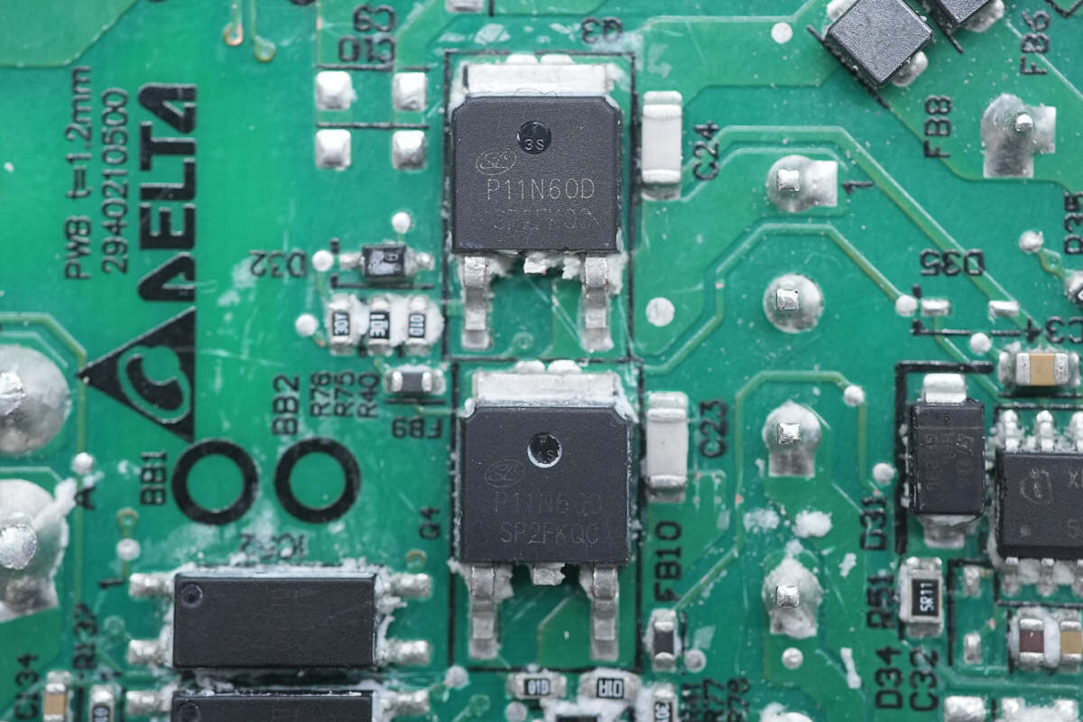
The HFB half-bridge MOSFET is from Silan and adopts TO-252 package. Model is SVSP11N60DD2TR. 600V 300mΩ.

Teardown of ASUS ROG 130W USB-C GaN Power Adapter (ADP-130HB B)-Chargerlab

Here is the resonant capacitor. 0.47μF 450V.

Teardown of ASUS ROG 130W USB-C GaN Power Adapter (ADP-130HB B)-Chargerlab

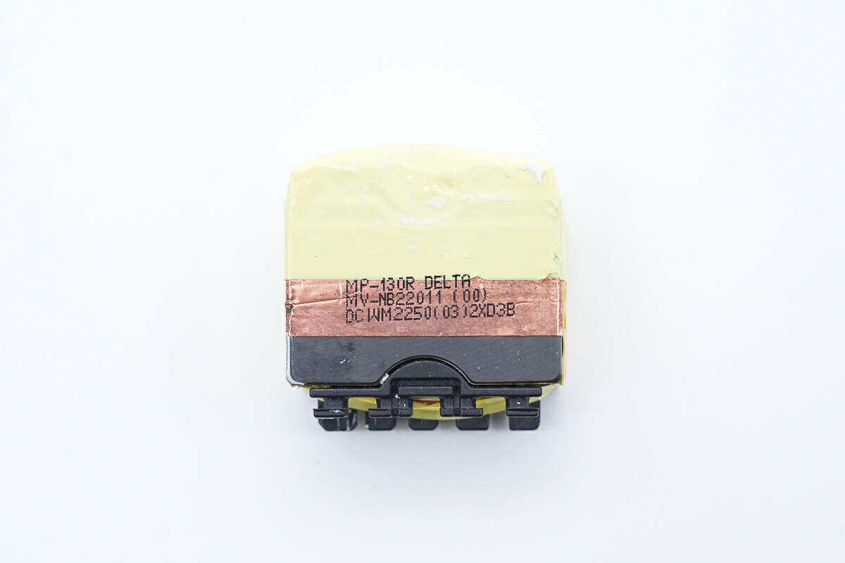
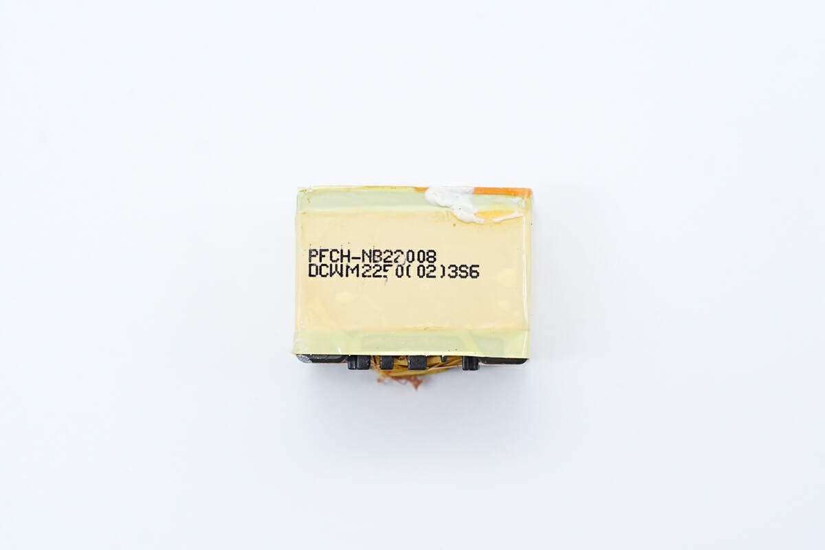
Here is the transformer.

Teardown of ASUS ROG 130W USB-C GaN Power Adapter (ADP-130HB B)-Chargerlab

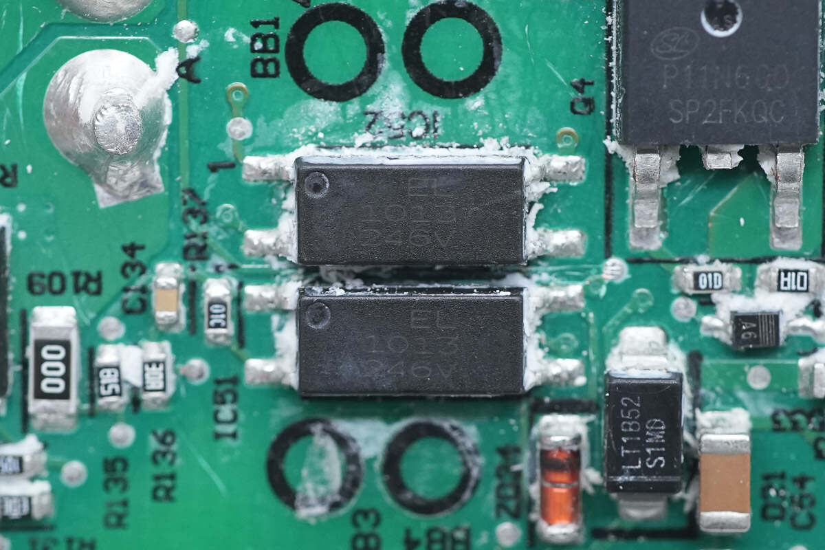
These two optocouplers for output voltage feedback and protection are from Everlight. Model is EL 1013.

Teardown of ASUS ROG 130W USB-C GaN Power Adapter (ADP-130HB B)-Chargerlab

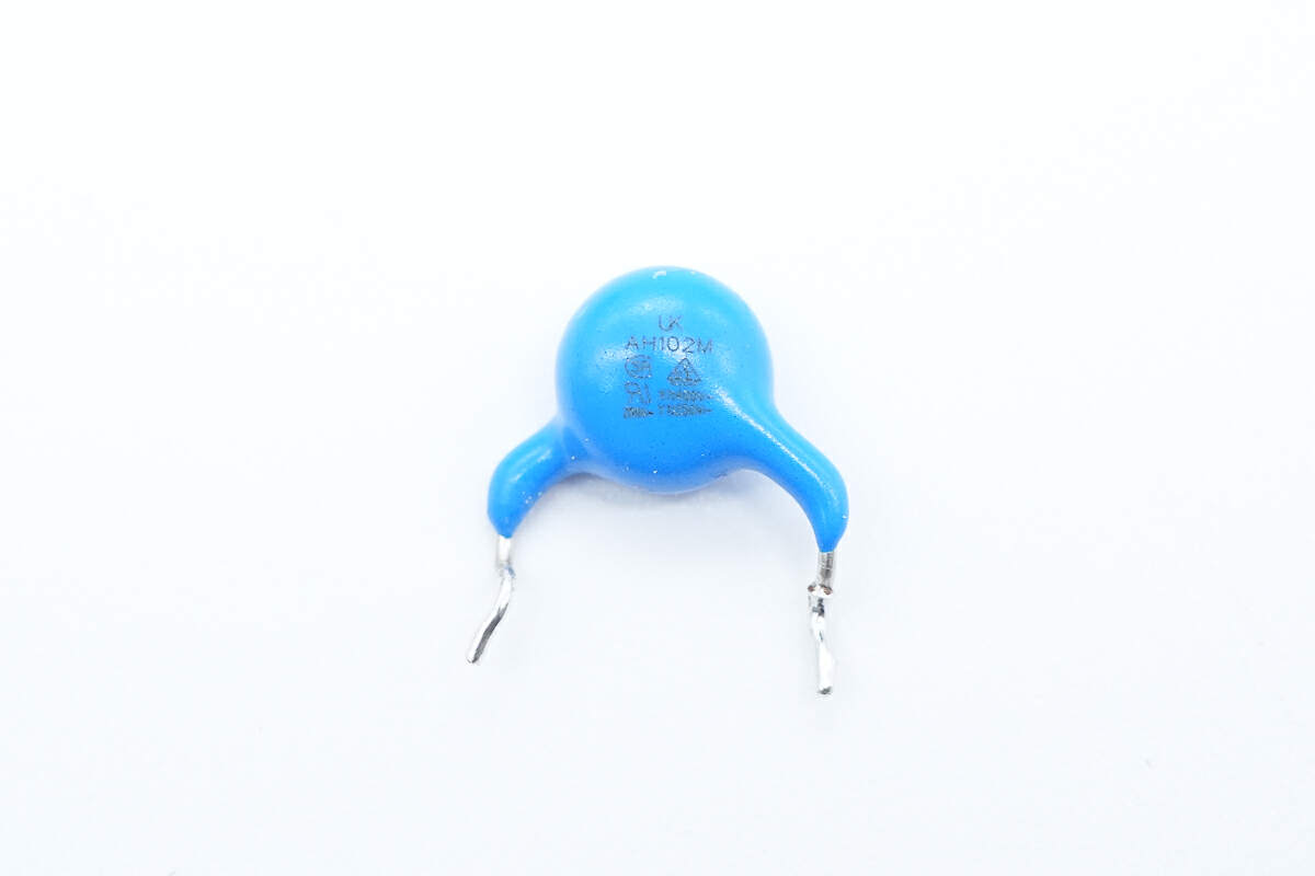
This is the blue Y capacitor.

Teardown of ASUS ROG 130W USB-C GaN Power Adapter (ADP-130HB B)-Chargerlab

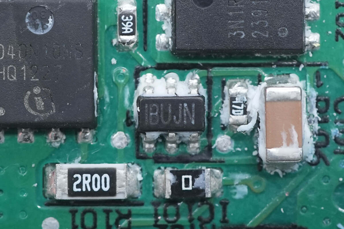
The synchronous rectifier controller marked with IBUJN is from MPS and adopts TSOT23-6 package. It supports DCM, CCM, QR, and ZVS operating modes, as well as ACF active clamp flyback and HFB hybrid flyback, with an operating frequency of up to 1MHz. It supports both high-side and low-side applications. Model is MP6951.

Teardown of ASUS ROG 130W USB-C GaN Power Adapter (ADP-130HB B)-Chargerlab

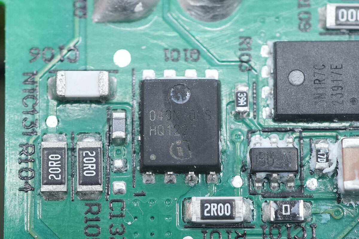
The synchronous rectifier is from Infineon and adopts PG-TDSON-8 package. Model is BSC040N10NS. 100V 4mΩ.

Teardown of ASUS ROG 130W USB-C GaN Power Adapter (ADP-130HB B)-Chargerlab

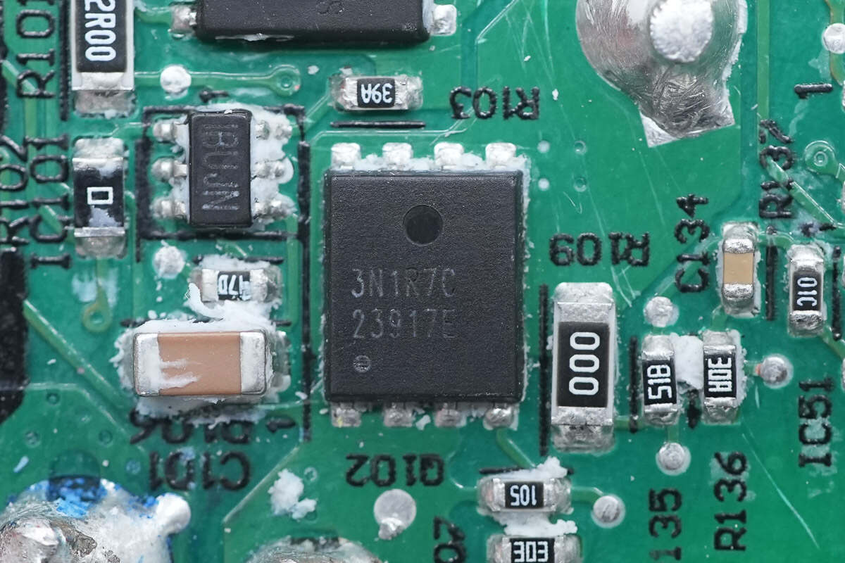
This MOSFET is marked with 3N1R7C.

Teardown of ASUS ROG 130W USB-C GaN Power Adapter (ADP-130HB B)-Chargerlab

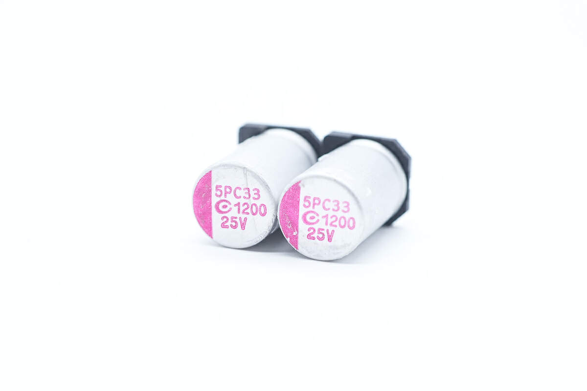
These two solid capacitors for output filtering are from APAQ. 25V 1200μF.

Teardown of ASUS ROG 130W USB-C GaN Power Adapter (ADP-130HB B)-Chargerlab

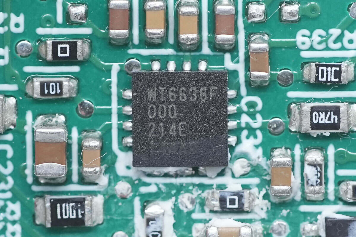
The protocol chip is from Weltrend. It has passed the USB-IF Association USB PD3.0 (PPS) certification and Qualcomm QC4+ certification. It supports USB PD3.0 and PPS, supports wire loss compensation, and supports multiple protection functions. It integrates 10-bit ADC for voltage and current detection, a built-in 8051 core microcontroller, and a built-in discharge MOSFET. Model is WT6636F.

Teardown of ASUS ROG 130W USB-C GaN Power Adapter (ADP-130HB B)-Chargerlab

Well, those are all components of the ASUS ROG 130W USB-C GaN Power Adapter.

Summary of ChargerLAB

Teardown of ASUS ROG 130W USB-C GaN Power Adapter (ADP-130HB B)-Chargerlab

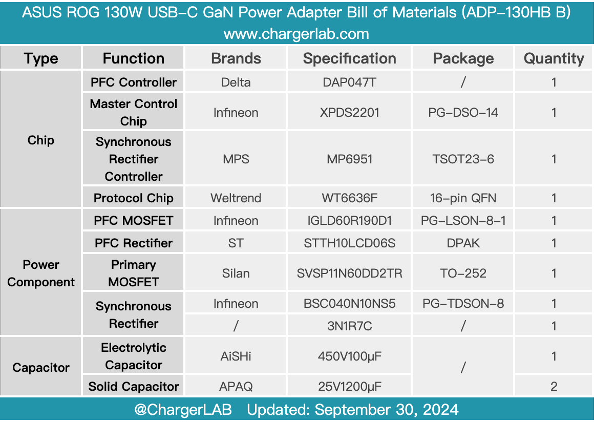
Here is the component list of the ASUS ROG 130W USB-C GaN Power Adapter.

The ASUS ROG 130W USB-C GaN Power Adapter features a black matte shell with a glossy ROG logo and comes with a 1.6-meter-long USB-C output cable. It adopts a detachable power cord design, and the power cord can be replaced with different lengths according to the usage scenario, making it convenient to use. The maximum power of 130W meets the power supply needs of laptops.

After taking it apart, we found the PCBA module is made up of multiple small PCBs, each with a copper heat sink. The components are reinforced with potting compound. The overall materials are luxurious, and the workmanship is solid and reliable.

Related Articles:
1. ASUS Launches ROG 140W USB-C GaN Charger for Multi-Device Fast Charging
2. Enhanced Gameplay: ROG Ally's Monitor Compatibility Explored
3. Charging Review of ASUS ROG Ally Handheld Gaming Console

130W ASUS ROG
1
Anker Unveils 165W Power Bank with Built-In Retractable Cable for High-Speed, On-the-Go Charging
Previous
Teardown of RICOMM 370W GaN Desktop Charger (RCD3701)
Next

Hot posts

Anker Prime Thunderbolt 5 Docking Station: 14 Ports, Dual 8K Support, and 140W Power Delivery
Charging Compatibility Test of Nintendo Switch 2 (Handheld Mode)
Teardown of vivo 90W FlashCharge GaN Charger
Teardown of Xiaomi 15S Pro 15th Anniversary Edition: Featuring 3nm Self-Developed SoC Xring O1

Related posts

RAVPower 45W Ultrathin PD GaN Charger In-Depth Teardown Review

RAVPower 45W Ultrathin PD GaN Charger In-Depth Teardown Review

August 7, 2019
6
GaN & PD3.1 | Teardown of UGREEN Nexode 300W 5-in-1 Charger

GaN & PD3.1 | Teardown of UGREEN Nexode 300W 5-in-1 Charger

March 18, 2024
0
Teardown of UGREEN 300W Nexode 5-in-1 Charger (CD333)

Teardown of UGREEN 300W Nexode 5-in-1 Charger (CD333)

March 30, 2024
0
Teardown of UGREEN 65W 3-in-1 Nexode RG GaN Charger (CD361)

Teardown of UGREEN 65W 3-in-1 Nexode RG GaN Charger (CD361)

May 1, 2024
4
1

ABOUT ME

As a sibling site of chongdiantou.com, ChargerLAB covers everything about charging, including chargers, wireless chargers, power banks, cables, car chargers, portable power stations and other peripherals. You can contact us by sending the email to info@chargerlab.com.

FOLLOW US

Facebook Instagram TikTok Twitter YouTube

E-COOL MEDIA

POWER-Z Chongdiantou 52Audio
Copyright © 2016-2025 Chargerlab. Designed by nicetheme.
  • News
    • What's New
    • Interviews
    • Vlogs
    • Events
    • Industry
  • Reviews
    • Charging Compatibility
    • Fully Charging
    • Comparison
    • Chargers & Cables
    • Power Banks & Stations
    • Mobile Devices
    • Accessories
  • Teardowns
    • Chargers & Cables
    • Power Banks & Stations
    • Power Supplies
    • Prototypes
    • Batteries
    • Accessories
  • Videos
    • YouTube
    • TikTok
  • Guides
    • How to Buy
    • Explained
    • Deals
    • ICs
  • POWER-Z
    • KM003C/KM002C
    • KT002
    • Buy POWER-Z
    • Technical Support
  • Contact Us
  • Apple
  • GaN
  • Power Bank
  • ANKER
  • 65W
  • iPhone 15
  • Qi2
  • ChargerLAB
  • USB-C
  • 100W

Rusell

Editor