Introduction
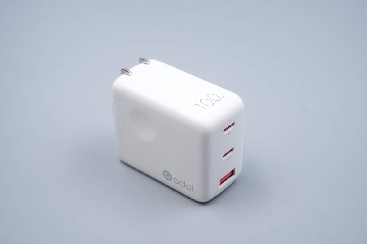
ASUS’s sub-brand Adol has launched a 100W GaN charger available in five stylish colors. The charger is equipped with two USB-C ports and one USB-A port, supporting outputs of 100W and 30W respectively, as well as output combinations such as 45W + 45W and 65W + 30W. In addition to compatibility with UFCS, QC, PD, and SCP protocols, it also supports Xiaomi’s proprietary 90W fast-charging protocol. The following provides a closer look at this product.
Product Appearance
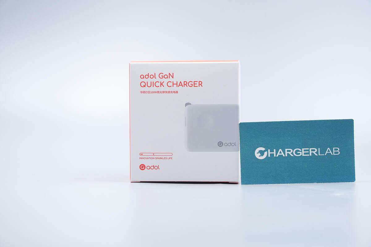
The front of the packaging features the Adol logo, the product name, and an image of the charger.
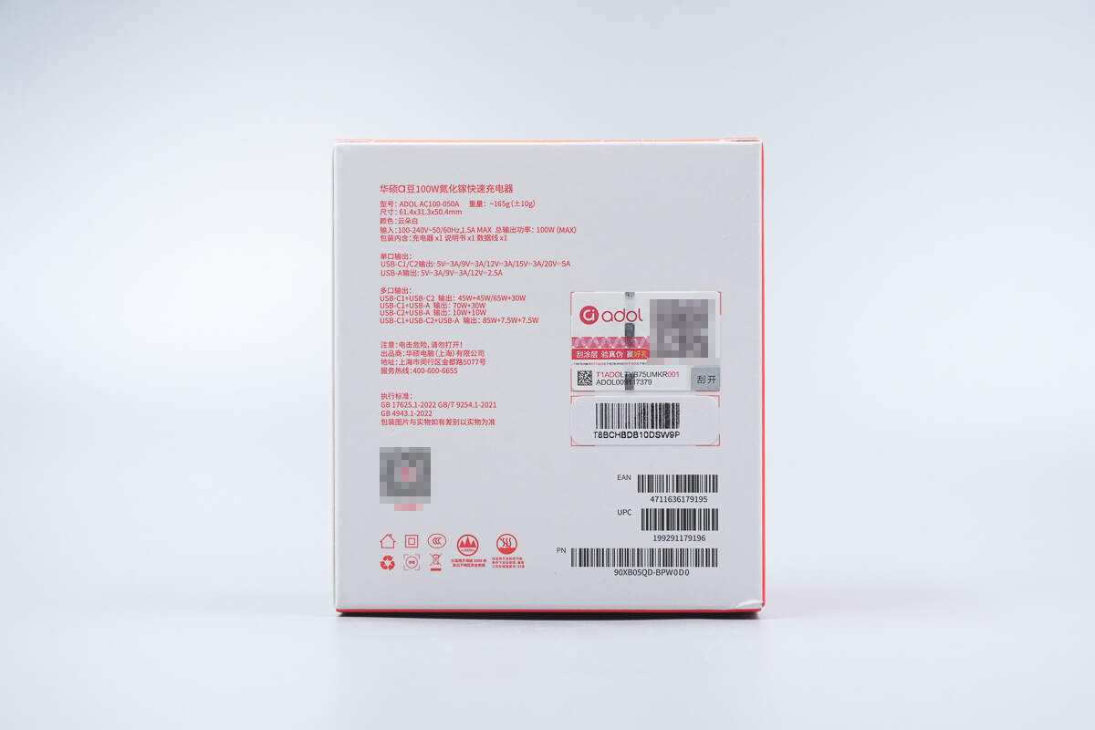
The back of the packaging displays the specifications, precautions, and certification information.
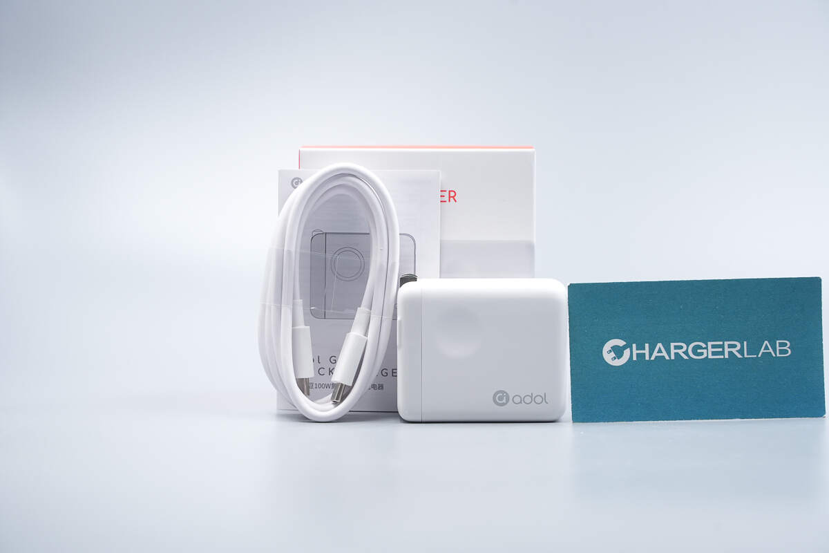
The package includes the charger, a data cable, and a user manual.
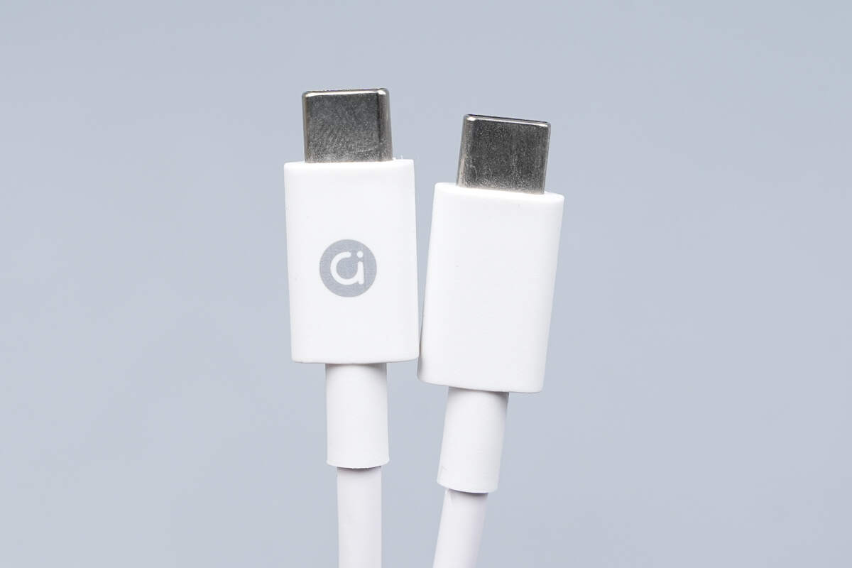
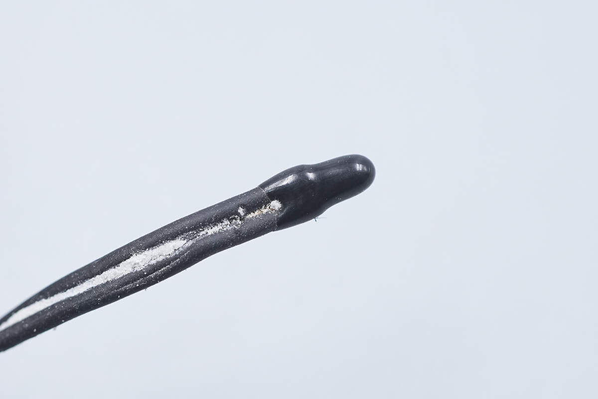
The included cable is a dual USB-C type, with the Adol logo printed on the connector.
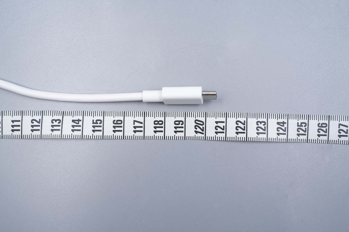
The length of the cable is about 120.5 cm (47.44 inches).
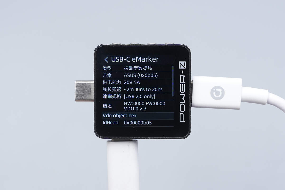
ChargerLAB POWER-Z KM003C shows it has an E-Marker chip. Its power transmission capability is 20V5A, and its data transmission capability is USB 2.0.
The housing is made of flame-retardant PC material.
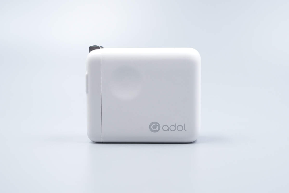
The front side features the Adol logo.
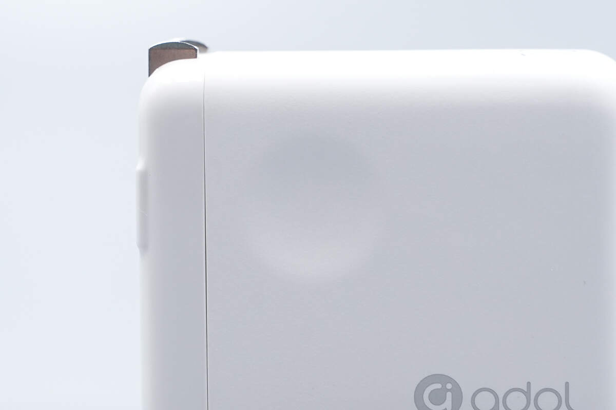
Both the front and back sides have grooves designed for easy plugging and unplugging.
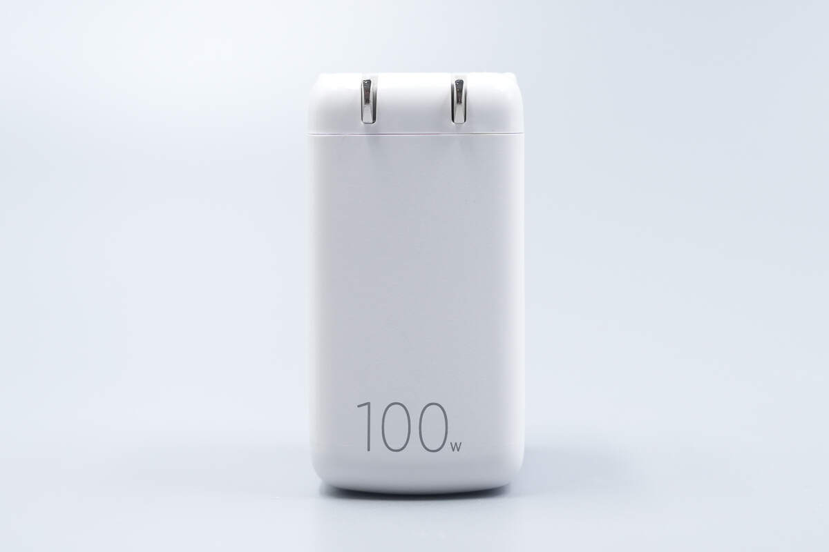
This side is marked with "100W".

The input port housing is marked with the specifications.
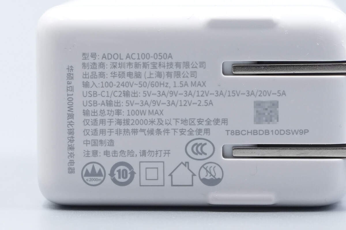
Model: ADOL AC100-050A
Input: 100-240V~50/60Hz 1.5A MAX
Output:
USB-C1/C2: 5V 3A, 9V 3A, 12V 3A, 15V 3A, 20V 5A
USB-A: 5V 3A, 9V 3A, 12V 2.5A
Total output power: 100W MAX
The charger has passed CCC certification.
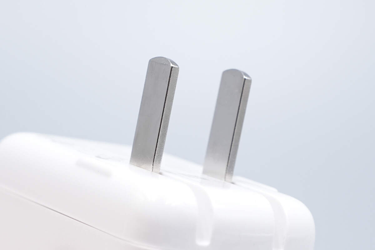
The charger comes with a foldable plug.
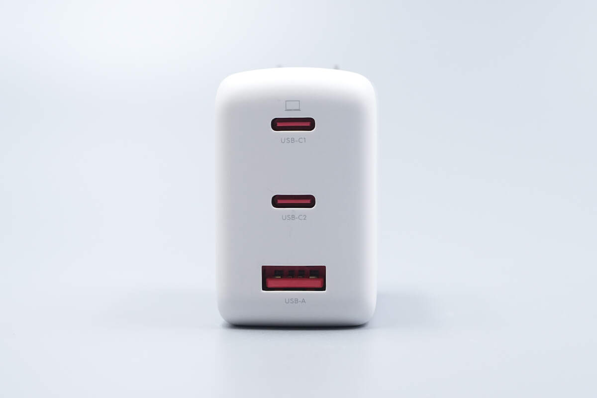
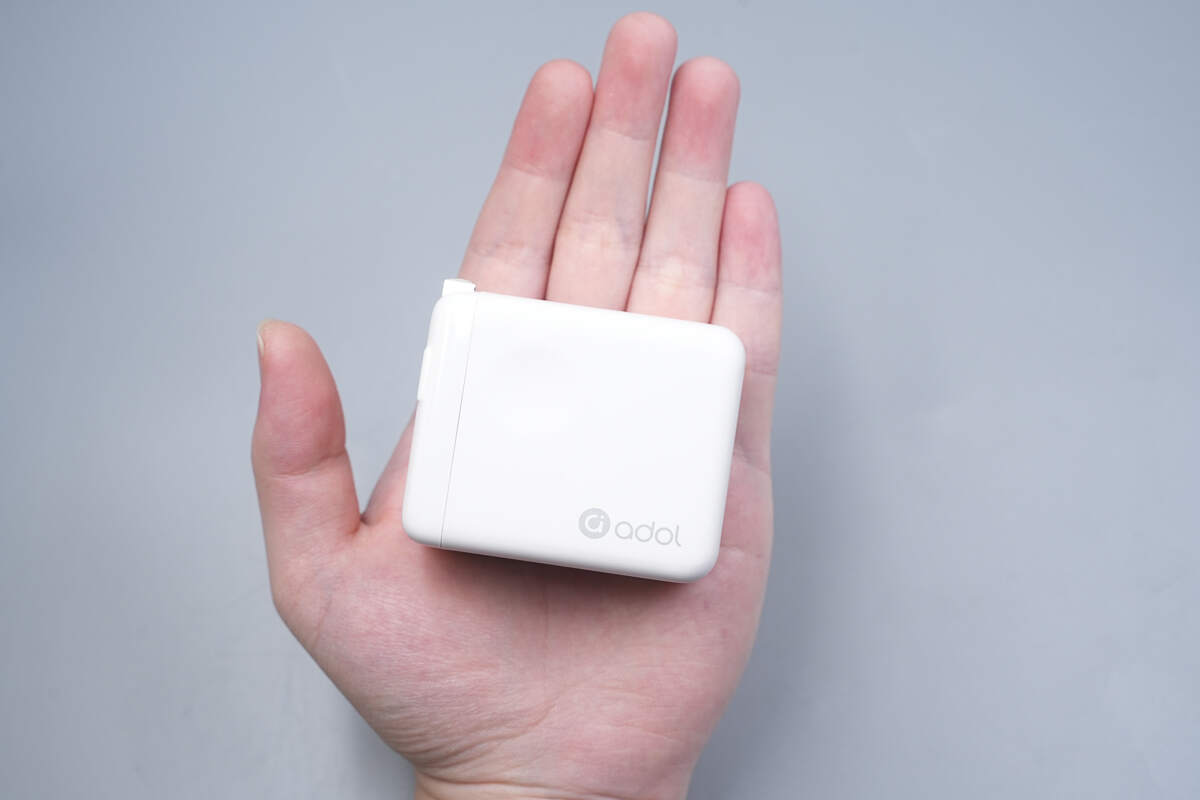
Equipped with two USB-C ports and one USB-A port.

The length of the charger is about 61.39 mm (2.42 inches).

The width is about 50.64 mm (1.99 inches).
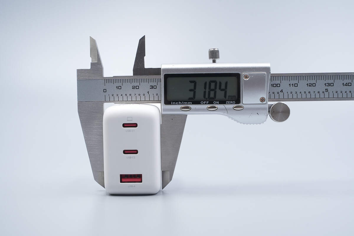
The thickness is about 31.84 mm (1.25 inches).
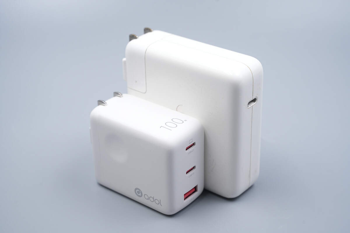
Compared with the Apple 96 W charger, its size advantage is obvious.
When compared side by side with Apple's 96W charger, its compact size is clearly advantageous.
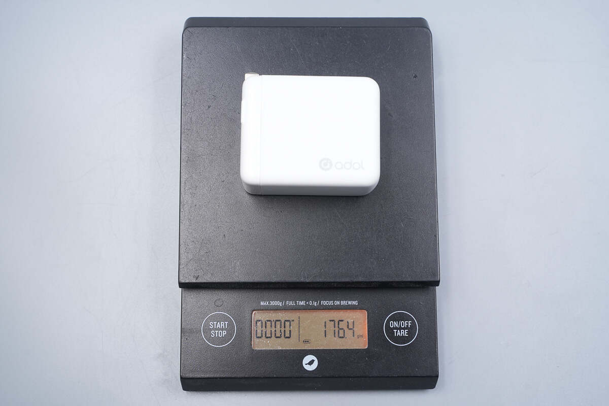
The weight is about 176 g (6.21 oz).
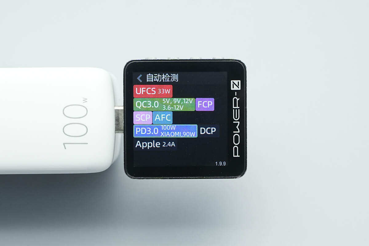
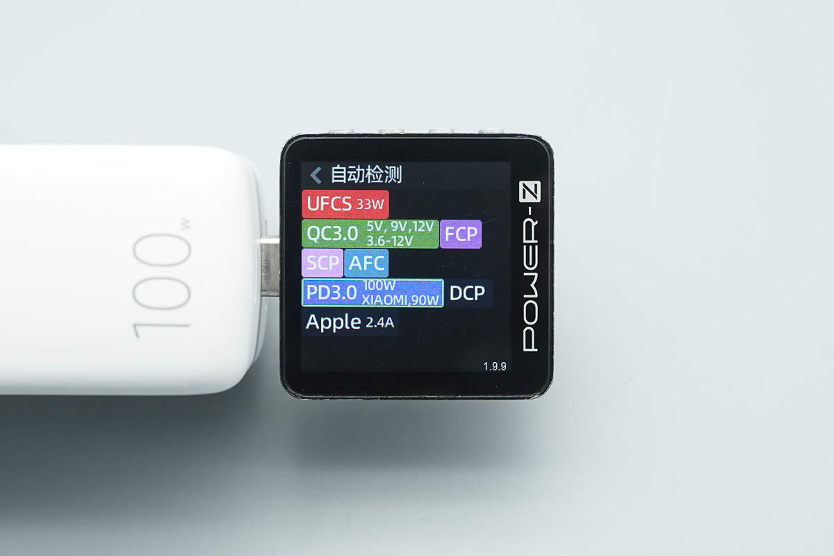
ChargerLAB POWER-Z KM003C shows that the USB-C1 supports UFCS, QC 3.0, FCP, SCP, AFC, PD 3.0, DCP, Apple 2.4A, and Xiaomi 90W proprietary protocol.
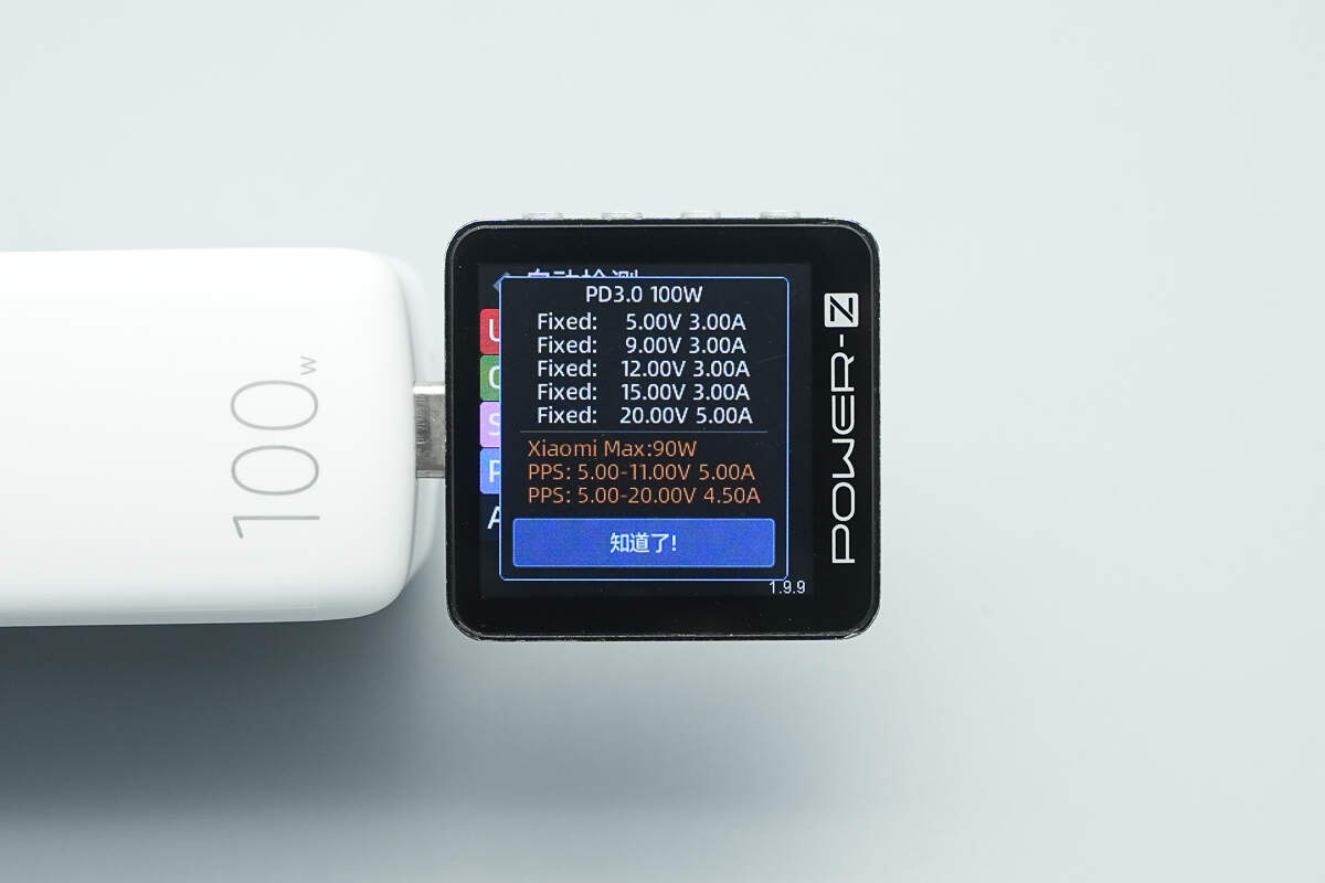
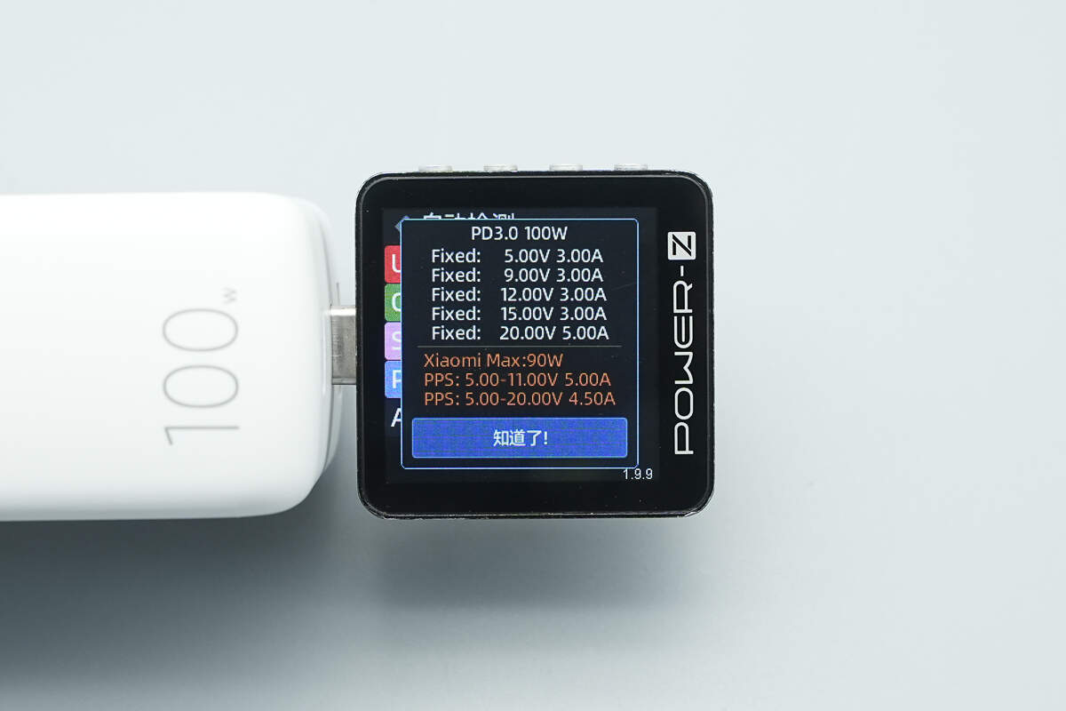
It has five fixed PDOs of 5V3A, 9V3A, 12V3A, 15V3A, and 20V5A, as well as two Xiaomi proprietary voltage levels: 5-11V5A and 5-20V4.5A.
The USB-C2 port is compatible with the same protocols as the USB-C1 port.
The PDO messages are identical as well.
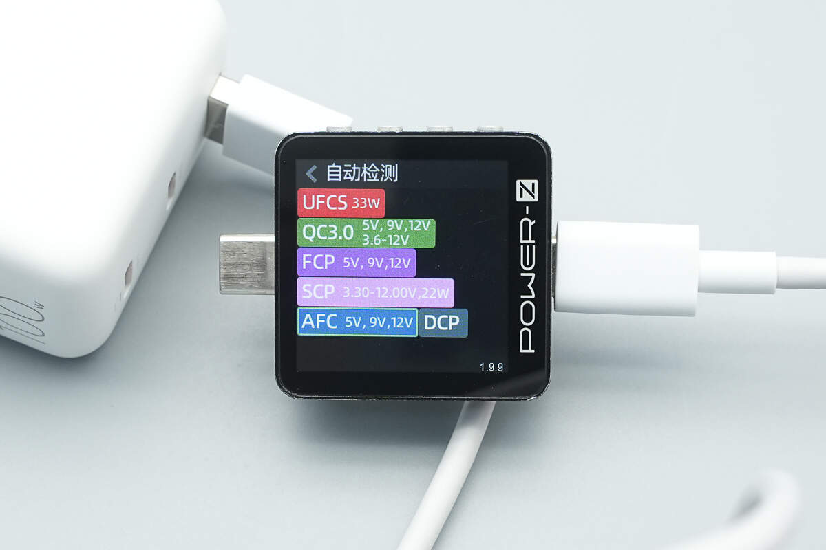
The USB-C1 supports UFCS, QC3.0, FCP, SCP, AFC, and DCP protocols.
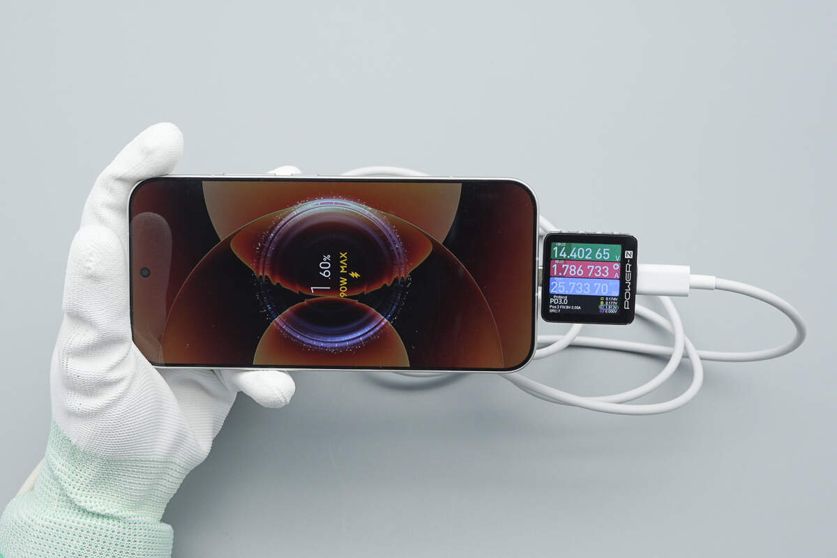
Using the USB-C1 port to charge the Xiaomi 17 Pro Max successfully activates Xiaomi’s 90W Surge Fast Charging.
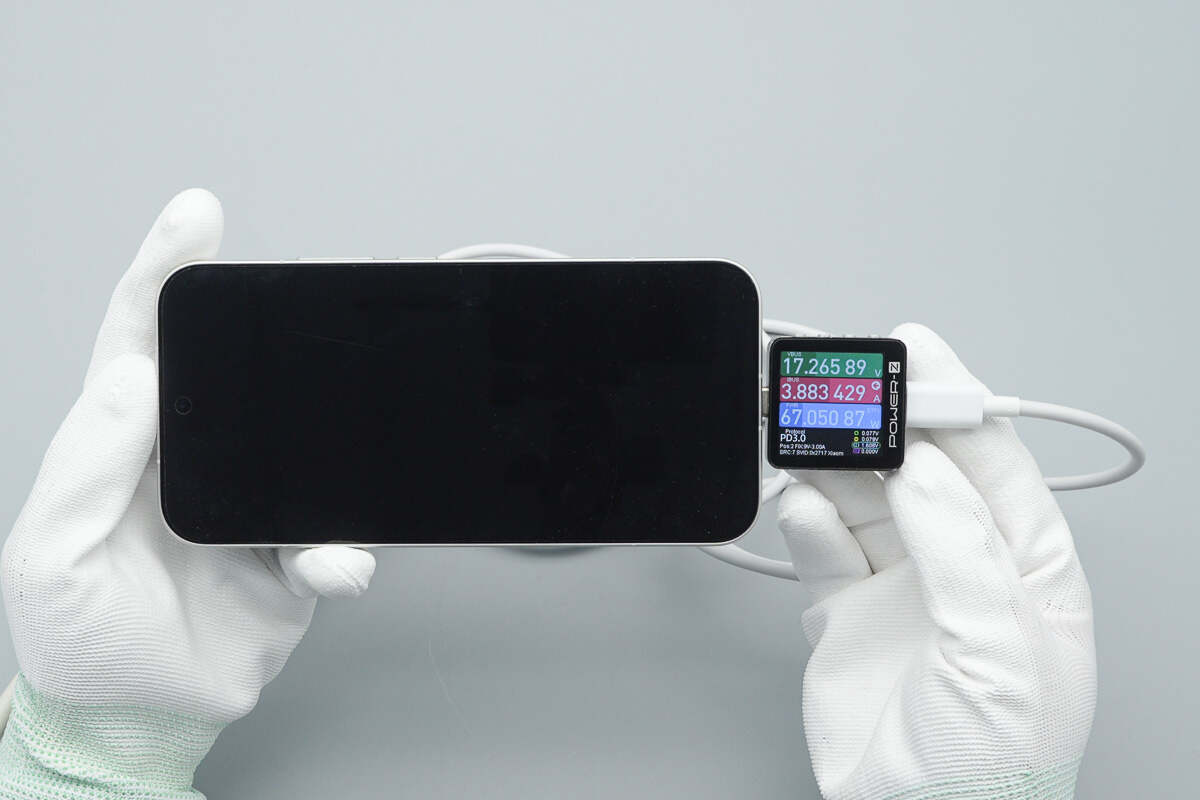
When the charging power reaches a stable state, the measured power is about 67.05W.
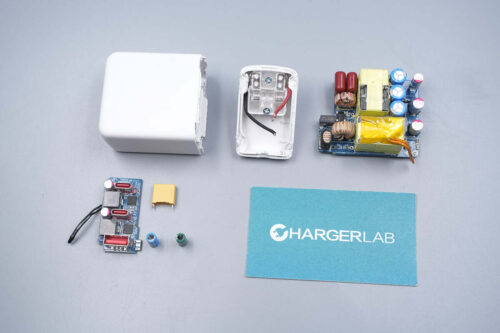
Teardown
Next, let's take it apart to see its internal components and structure.
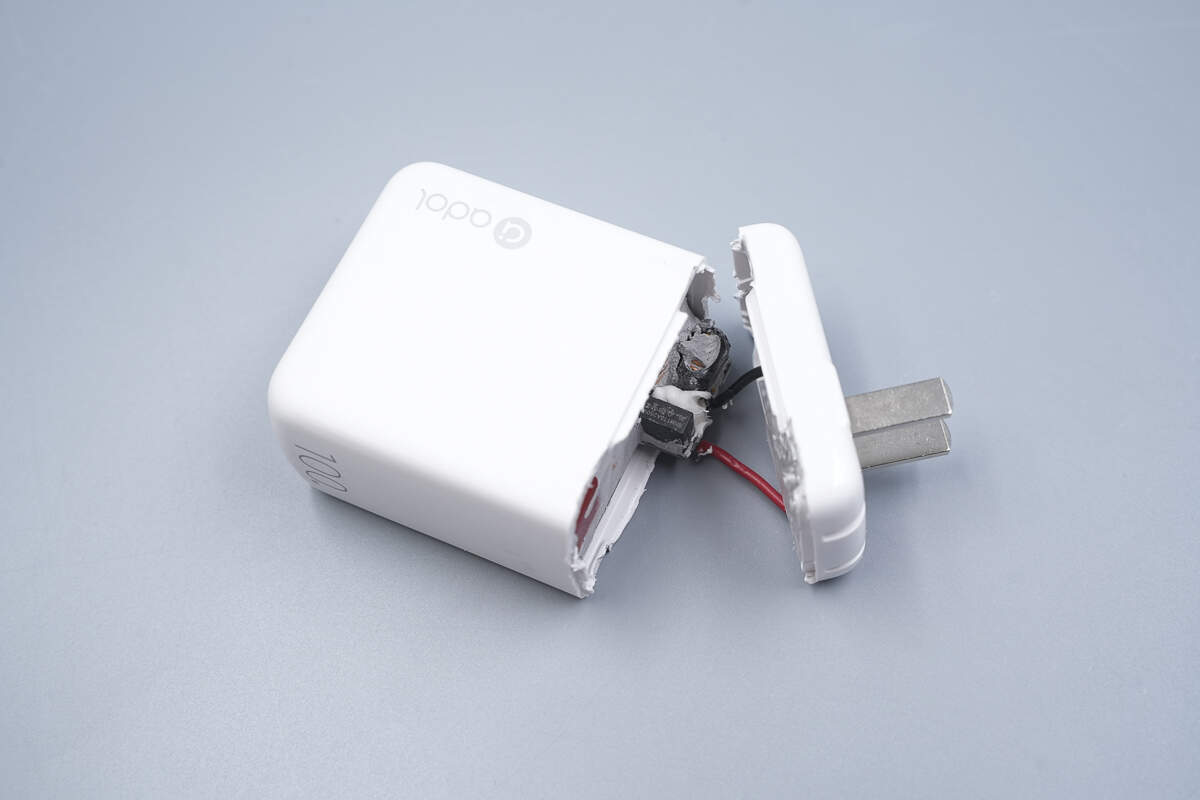
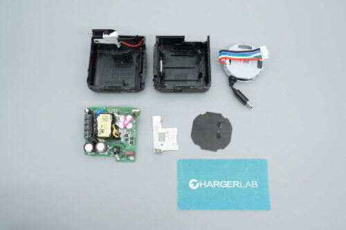
Remove the input casing. The pins are connected to the PCBA module via wires.
The interior of the charger is filled with potting compound for fixation.

Remove the PCBA module.
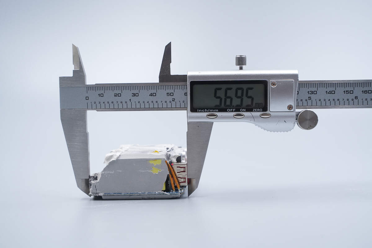
The length of the PCBA module is about 56.95 mm (2.24 inches).
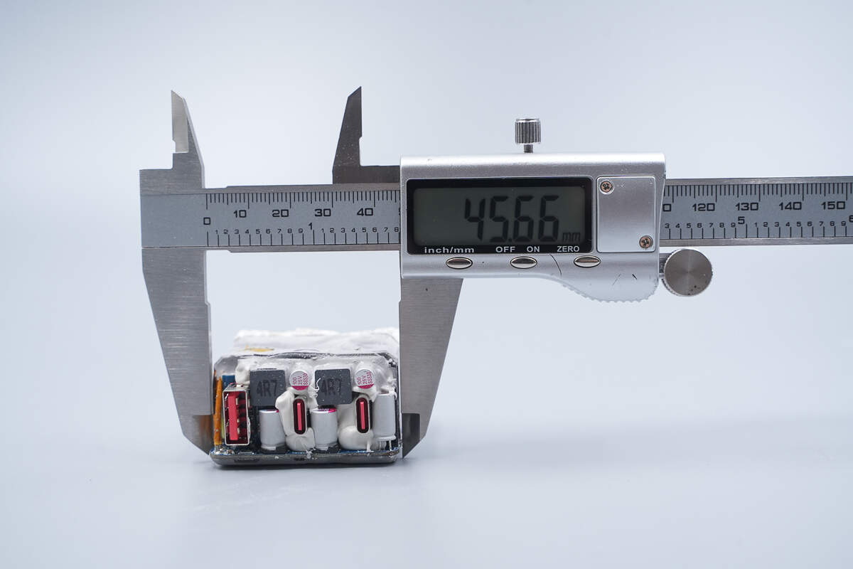
The width is about 45.66 mm (1.8 inches).
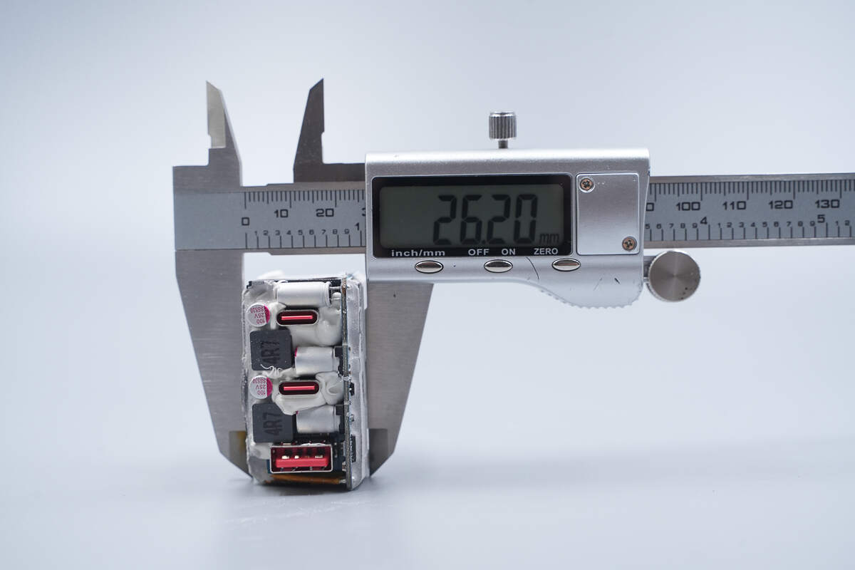
The thickness is about 26.2 mm (1.031 inches).
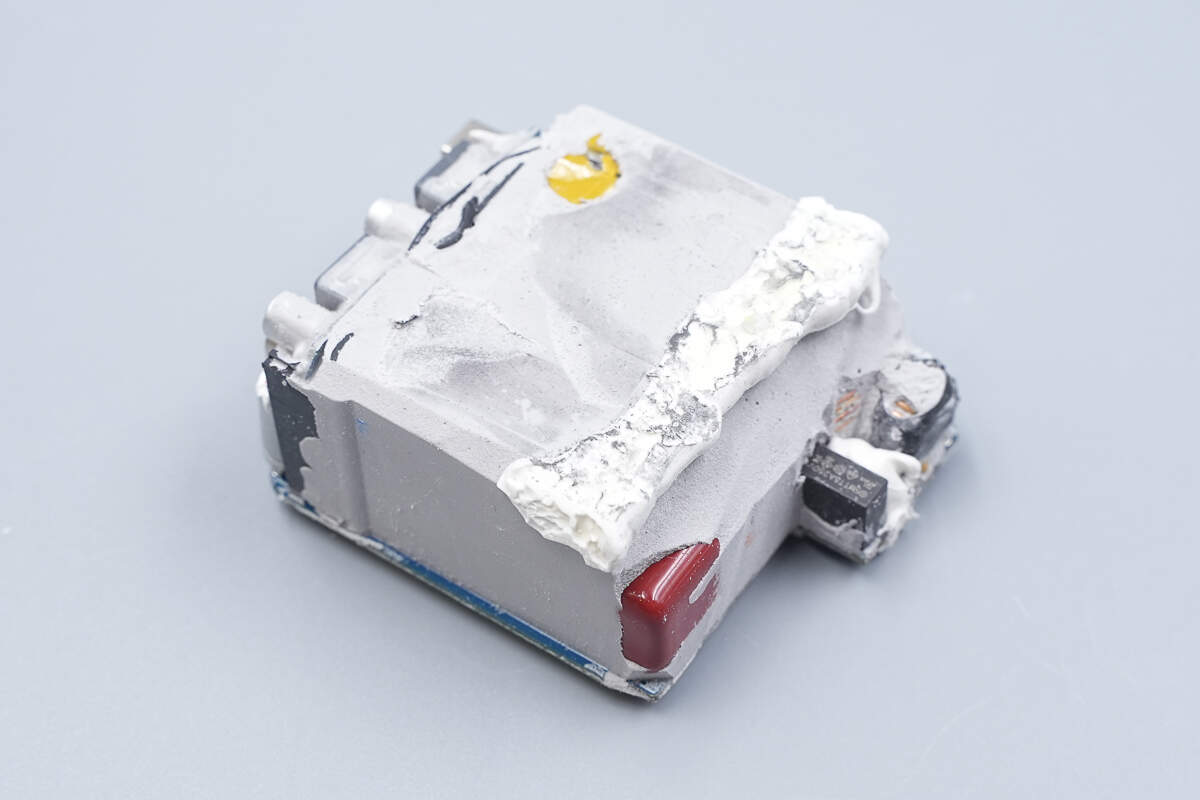
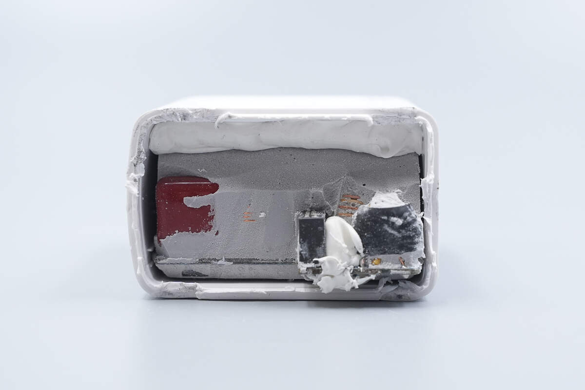
The entire PCBA module is potted to enhance heat dissipation and environmental durability.
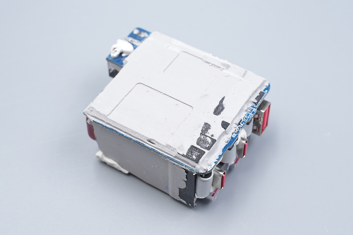
The bottom of the module is also fully covered with thermal conductive adhesive.
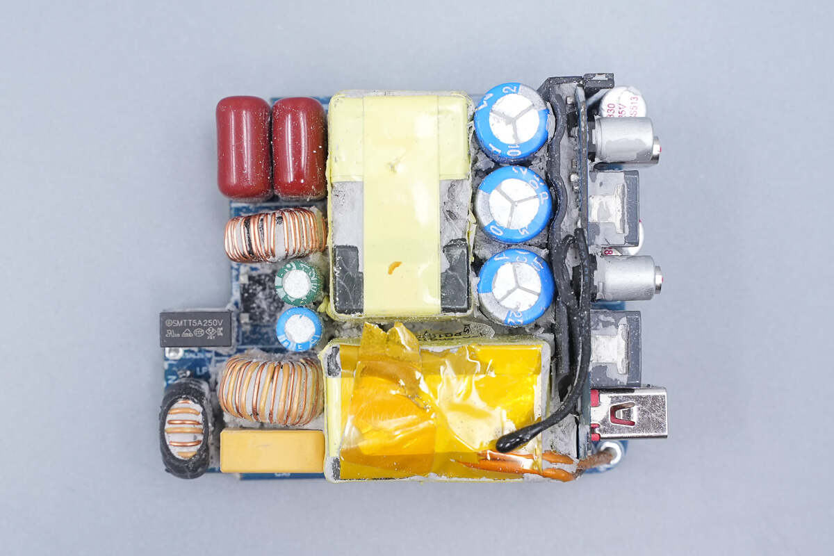
Remove the thermal conductive adhesive. The components on the front are densely arranged. A plastic isolation sheet is placed between the electrolytic capacitors and the output PCB. A thermistor is installed to monitor the temperature of the transformer.

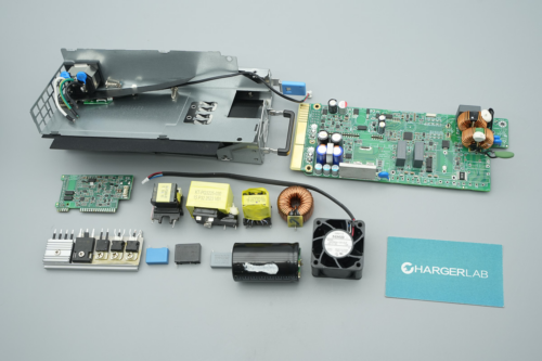
On the back side, there are bridge rectifiers, a PFC controller, a PFC MOSFET, a PFC rectifier, a master control chip, an optocoupler, an SMD Y capacitor, a synchronous rectifier controller, and a synchronous rectifier.
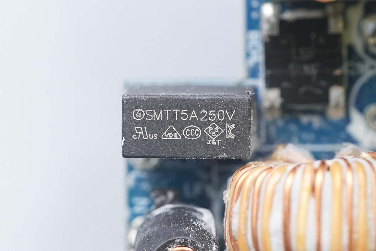
The time-delay fuse is rated at 5 A, 250 V.
The common mode choke is used to filter EMI interference and is insulated with a heat-shrink tube for protection.
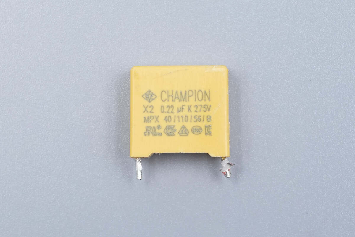
The safety X2 capacitor, sourced from CHAMPION, is rated at 0.22 μF.
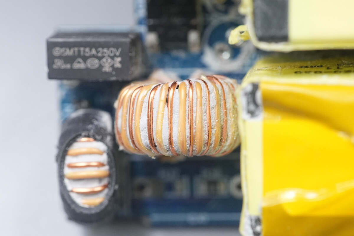
Close-up of the secondary common mode choke.
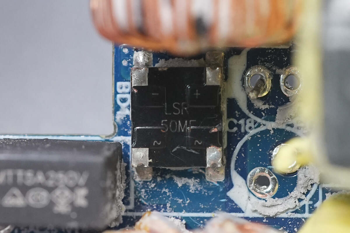
The bridge rectifier is from ZOWIE, model LSR50MF, rated at 5A 1000V, housed in a Z4PAK-SF package.
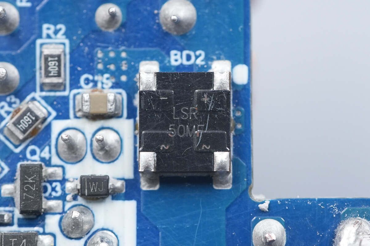
Another bridge rectifier with the same part number is located on the back side of the PCBA.
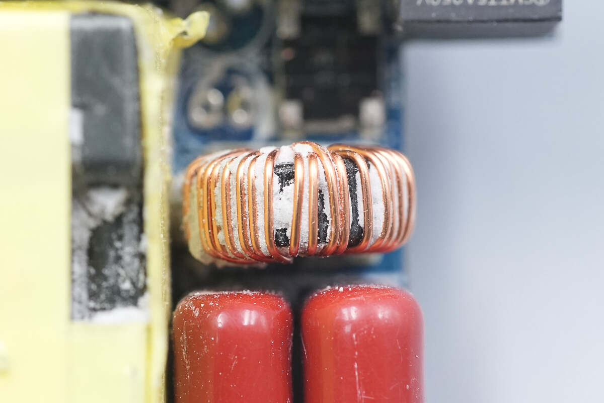
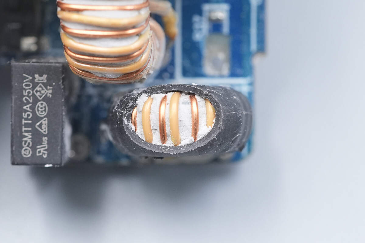
Close-up of the filter inductor.
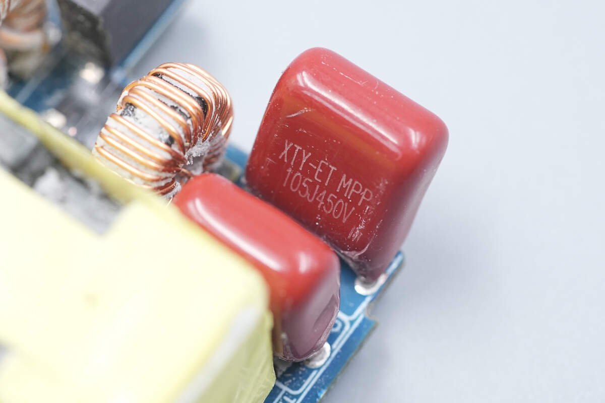
The two film capacitors have the same part number and are both 1μF 450V.
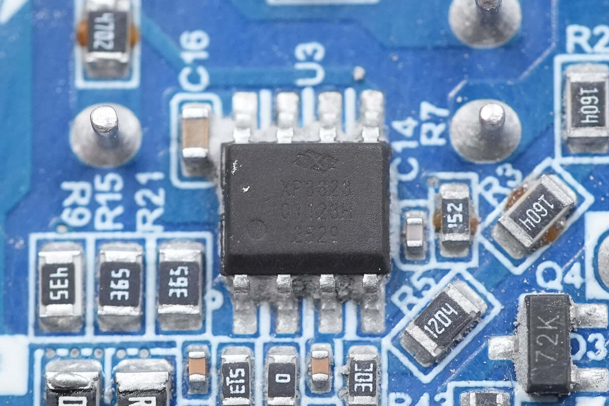
The PFC controller is from X-Signal, model XP3323. It is a boundary-mode PFC controller that utilizes a patented digital power control algorithm, offering excellent dynamic performance as well as high power factor (PF) and low total harmonic distortion (THD) under light load conditions. It is available in an SOP8 package.
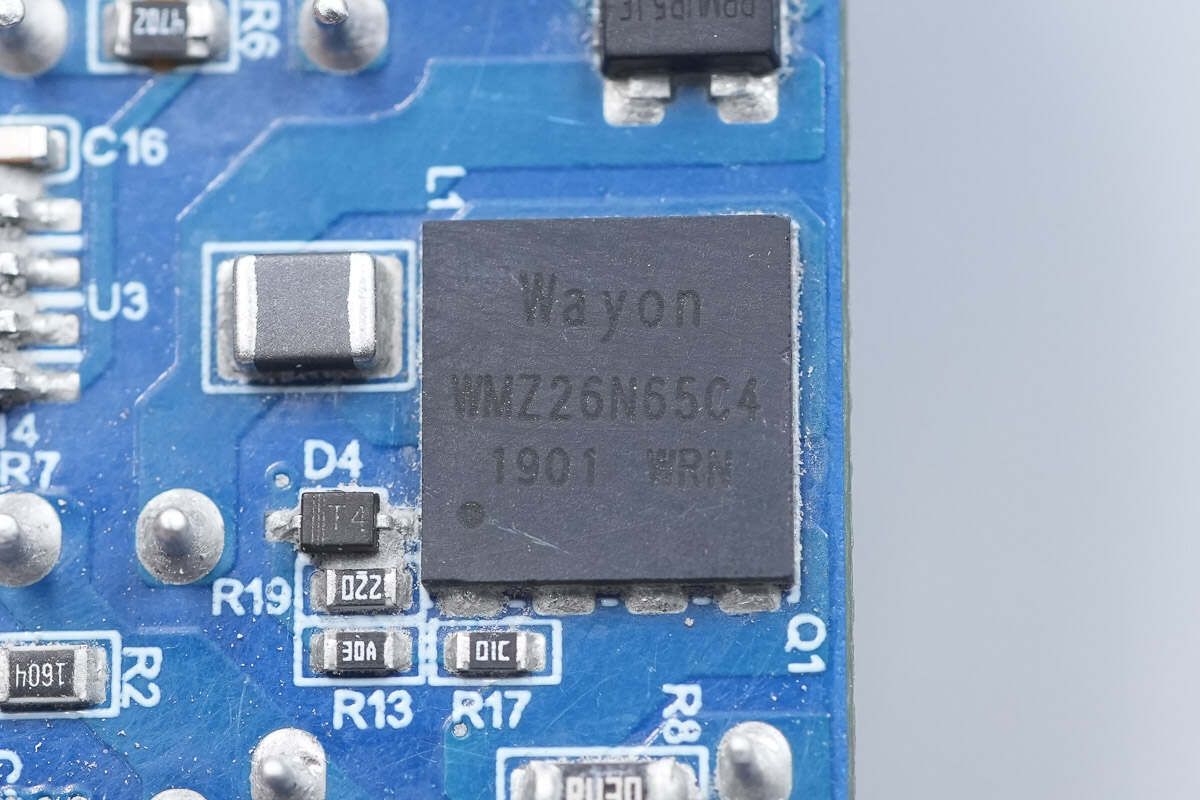
The PFC boost MOSFET is from WAYON, model WMZ26N65C4. It is a superjunction MOSFET with a voltage rating of 650 V and an on-resistance of 0.16 Ω, packaged in an 8×8 mm DFN.
Close-up of the PFC boost inductor.
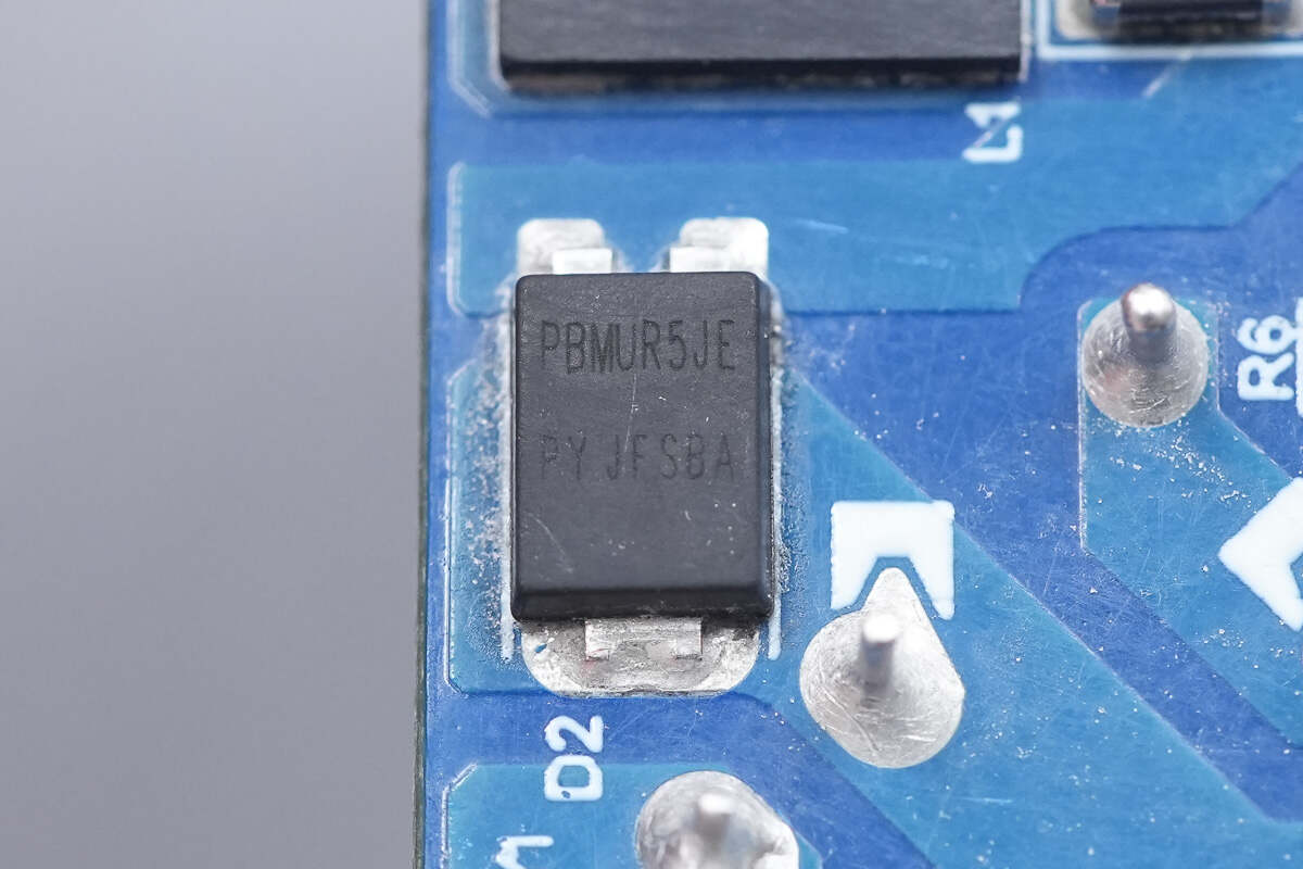
The PFC rectifier is from Pingwei, model PBMUR5JE. It is an ultra-fast recovery diode rated at 5 A and 600 V, featuring low forward voltage drop and high surge current capability, and is housed in a PS-277B package.
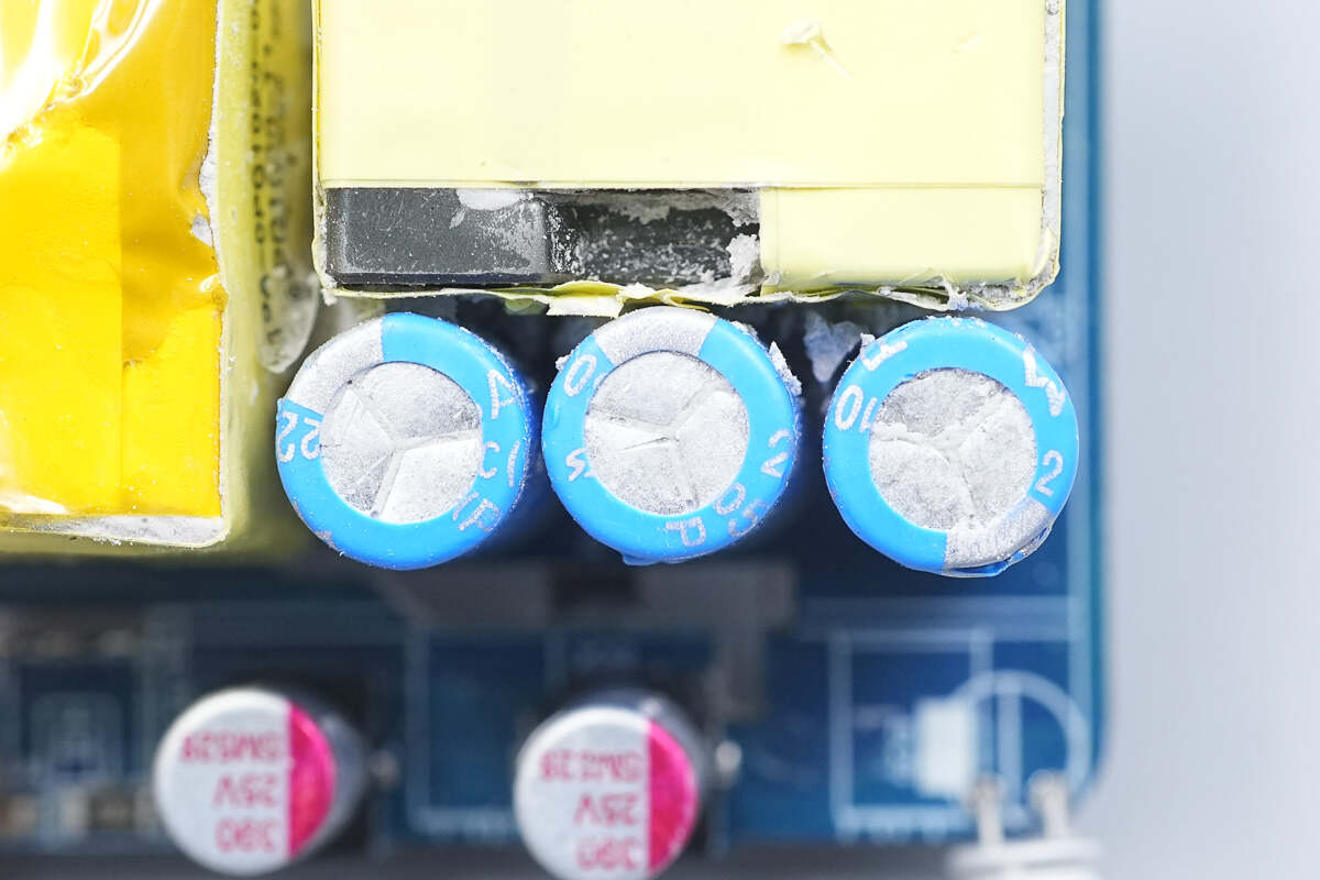
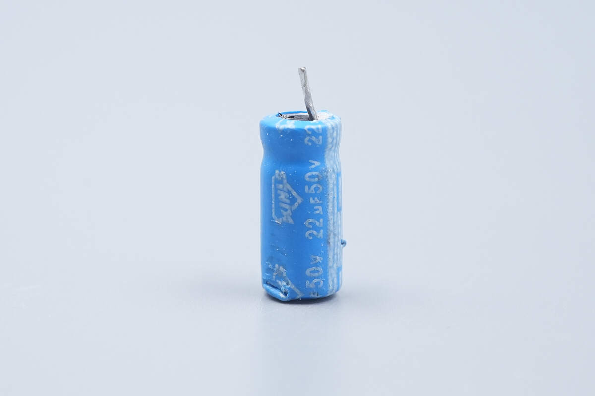
The three high-voltage filter electrolytic capacitors share the same part number.
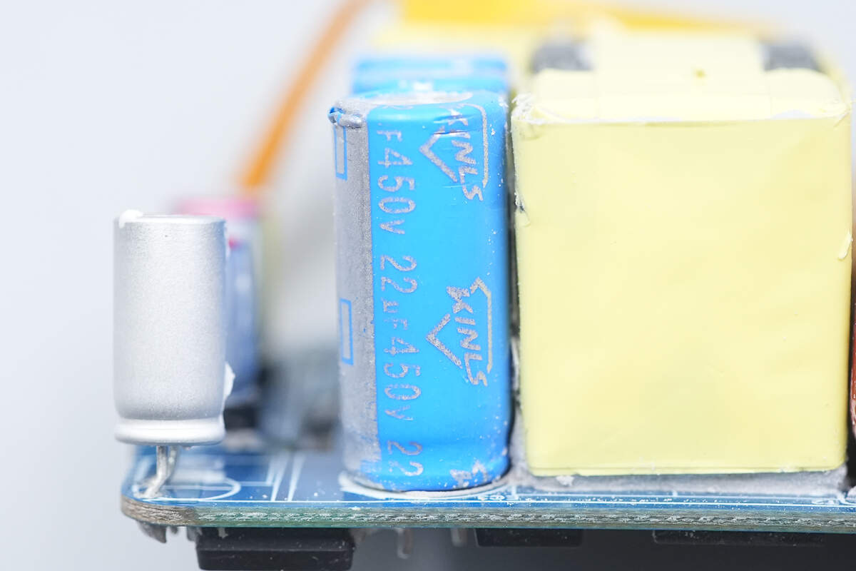
The capacitors come from KINLS, each with a specification of 450 V, 22 μF.
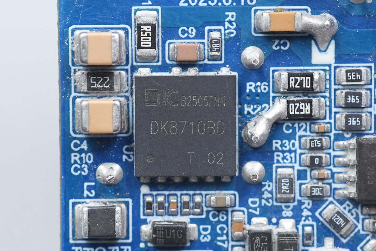
The master control chip is from DONGKE, model DK8710BD. It is an asymmetric half-bridge AC-DC switch integrating two GaN power devices, enabling ZVS on the primary and ZCS on the secondary for higher efficiency and reduced switching stress. The chip simplifies AC-DC converter design, supports high efficiency and power density, and includes protections such as overload, short-circuit, overvoltage, over/under VCC, and over-temperature. It is packaged in DFN 8×8.
Here is the information about DONGKE DK8710BD.
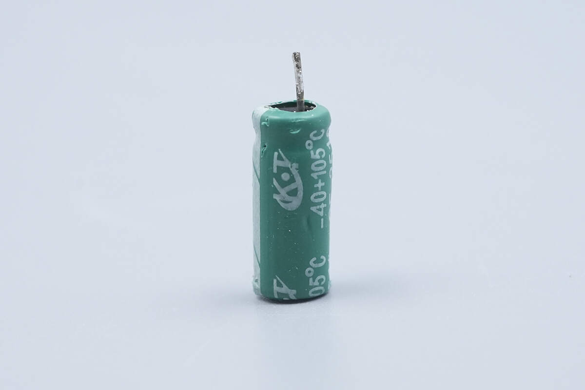
The capacitor supplying power to the master control chip is from KINLS, with a specification of 50 V, 22 μF.
The other capacitor is from KT.
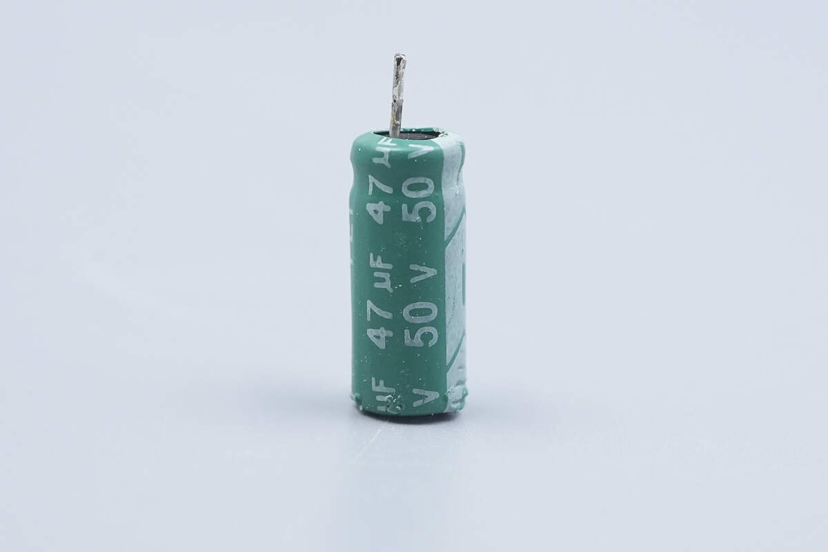
It has a specification of 50 V, 47 μF.
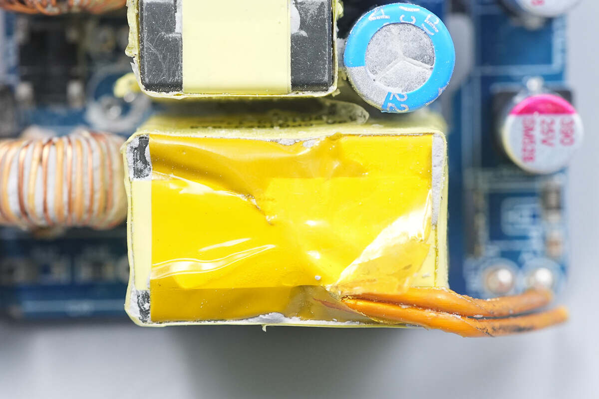
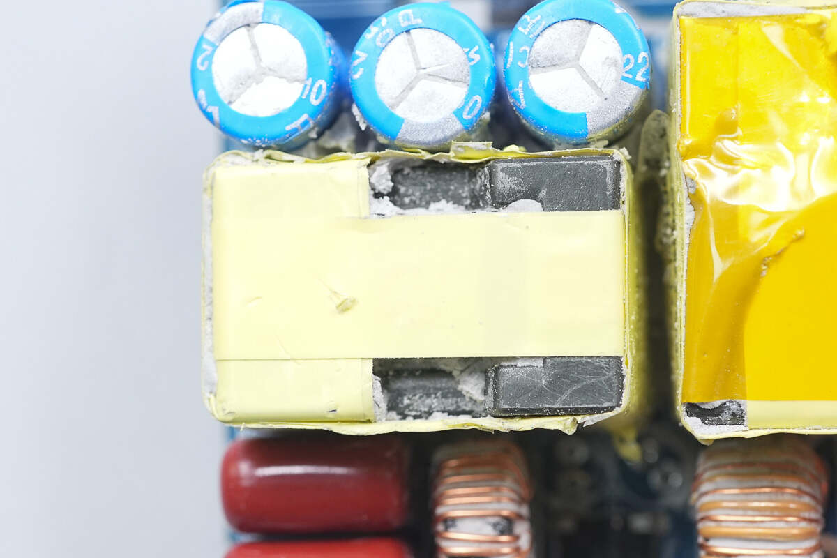
Close-up of the transformer.
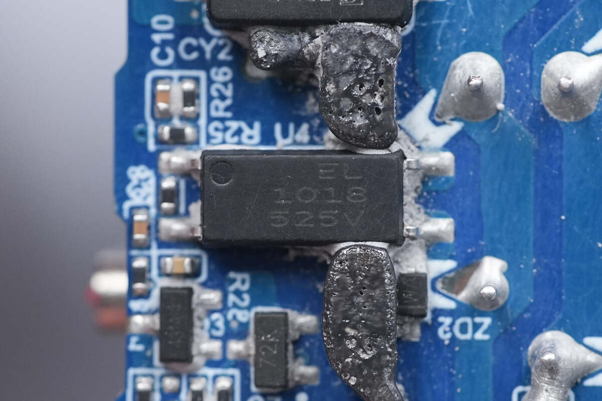
The Everlight EL1018 optocoupler is used for output voltage feedback.
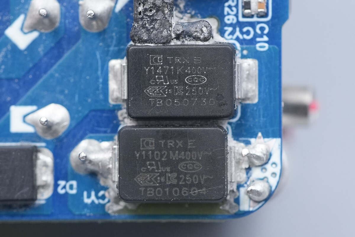
The SMD Y capacitors are from TRX, with part numbers TMY1102M and TMY1471K. Their compact size and light weight make them ideal for high-density power products, such as GaN fast chargers.

The synchronous rectifier controller, marked IBHJP, is from MPS, model MP6908A. It supports a maximum operating frequency of 600 kHz and multiple modes, including DCM, CCM, QR, and ACF. It can be used for both high-side and low-side applications, features ringing detection to prevent false turn-on, and is packaged in a TSOT23-6.
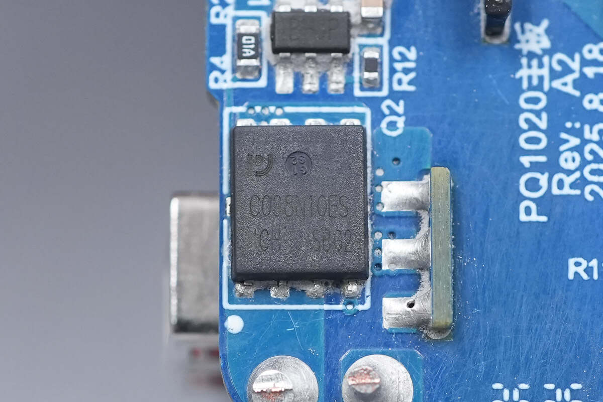
The synchronous rectifier is from Pingwei, model PWC038N10ES. It is an N‑channel MOSFET with a voltage rating of 100 V and an on-resistance of 3 mΩ, packaged in a 5×6 mm DFN.
The synchronous rectifier is from Pingwei, model PWC038N10ES. It is an N‑channel MOSFET with a voltage rating of 100 V and an on-resistance of 3 mΩ, packaged in a 5×6 mm DFN.
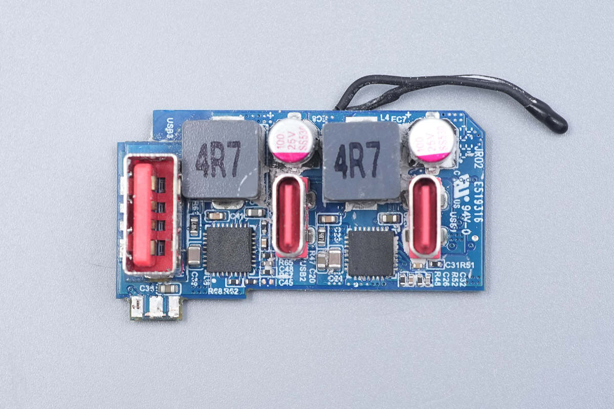
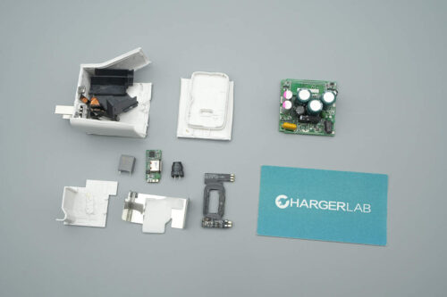
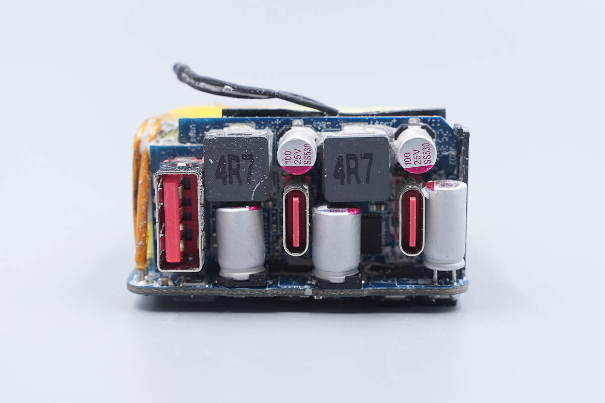
Remove the output PCB. Its front side is equipped with synchronous buck converters, buck inductors, and solid capacitors for output filtering.

The back side features protocol chips, output VBUS MOSFETs, and a thermistor.
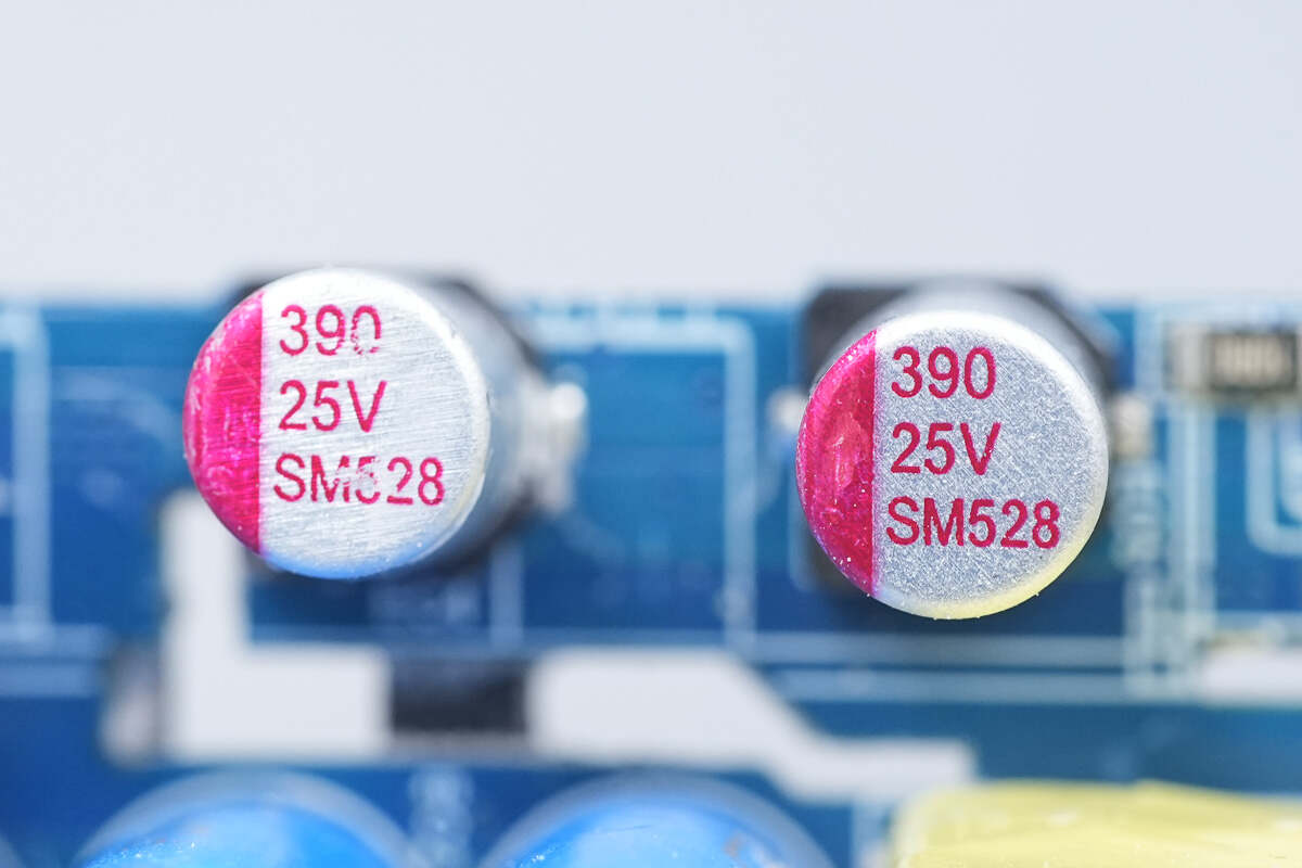
The two solid capacitors are each rated at 25 V, 390 μF.

The other solid capacitor is rated at 25 V, 330 μF.
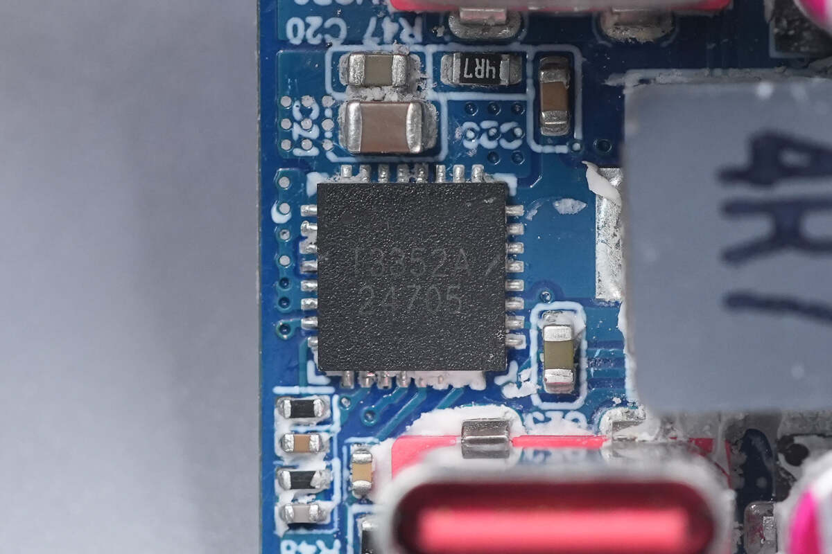
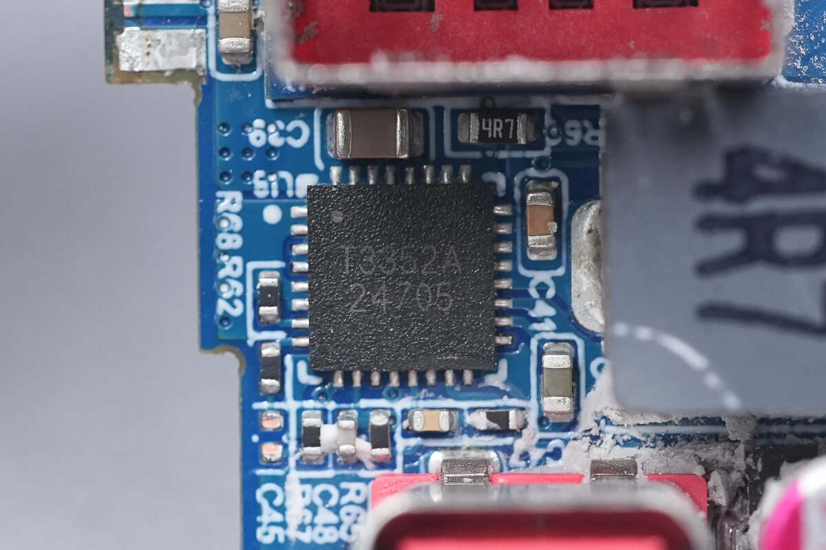
The USB-C1 synchronous buck converter is from Tollsemi, model TMI3352A. It is an integrated dual-switch synchronous buck converter designed for applications with a wide input voltage range. The device uses current-mode control to achieve optimal performance under transient conditions. When the input voltage is significantly higher than the regulated output, it operates in standard buck mode; when the input voltage is close to the output, it automatically switches to a low-dropout mode with a duty cycle up to 99.5%.
The TMI3352A features fixed soft-start and multiple protection mechanisms, including input undervoltage lockout, overvoltage protection, cycle-by-cycle current limit, output average current limit, and over-temperature shutdown. It comes in a compact QFN 5×5-32 package.
The synchronous buck converter for the other USB-A and USB-C ports also uses the Tollsemi TMI3352A.
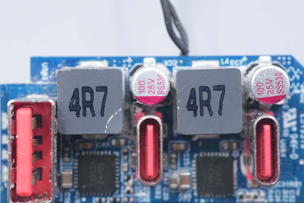
Each of the two buck circuits is paired with a 4.7 μH inductor.
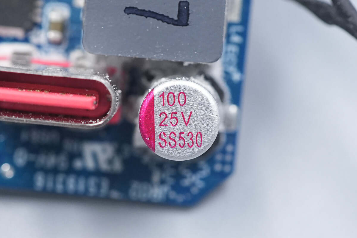
This buck output filtering solid capacitor is rated at 25 V, 100 μF.
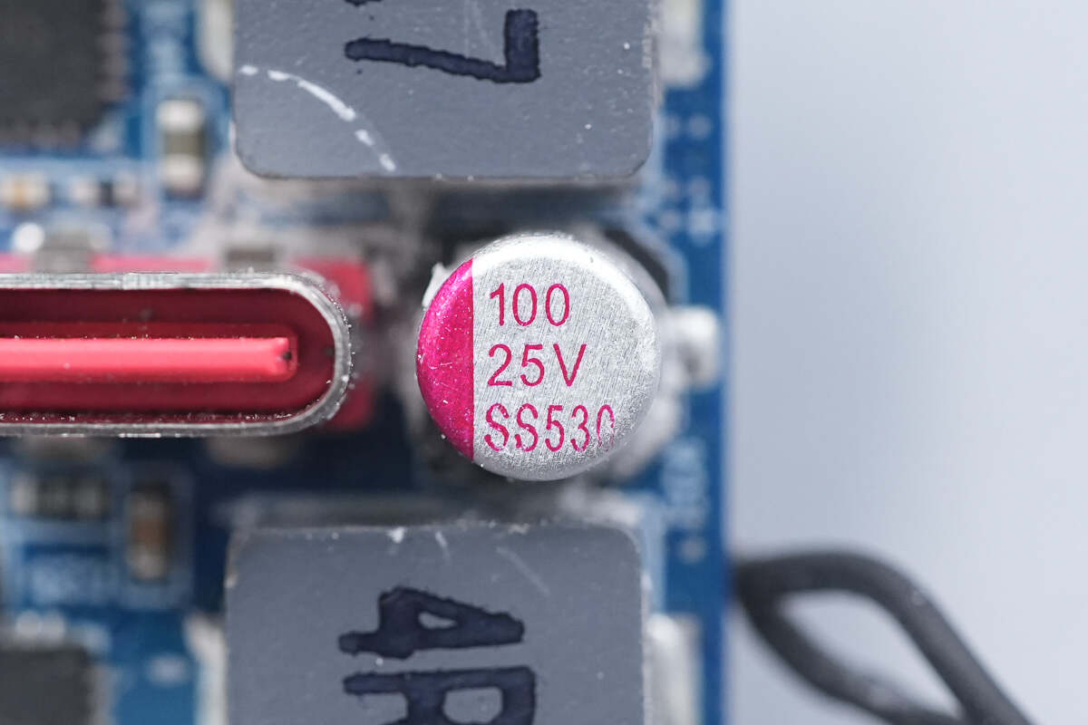
The other capacitor has the same specification of 25 V, 100 μF, and shares the same part number.
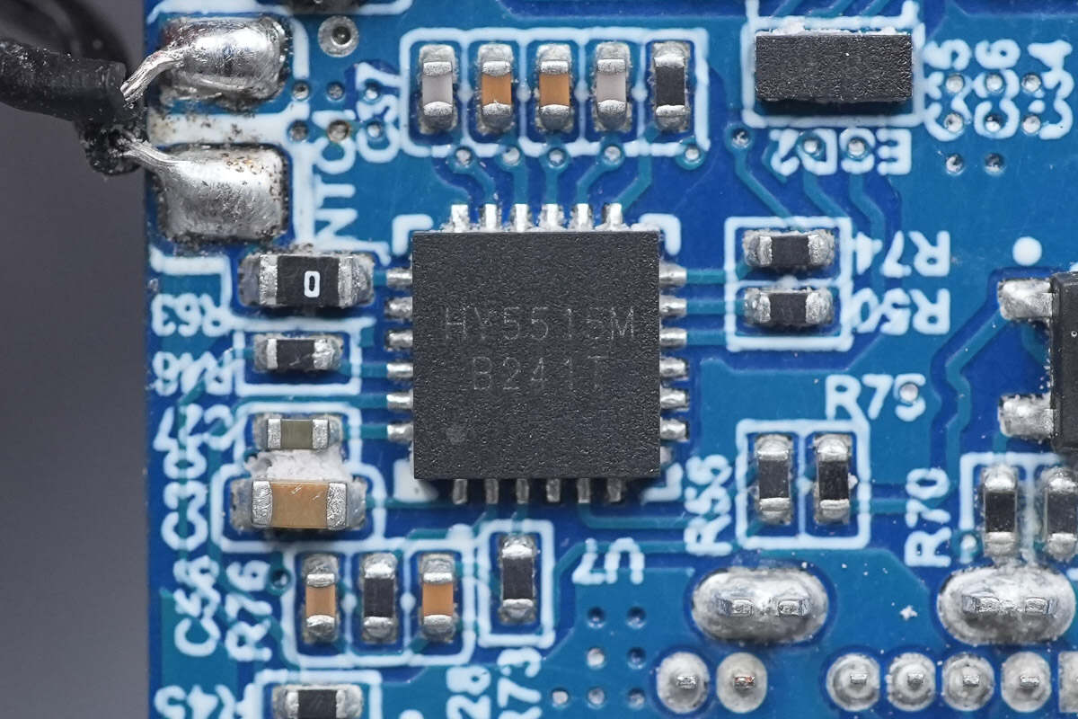
The USB-C1 protocol chip is from HYASiC, model HY5515M. It features a built-in 32-bit MCU with 32 KB MTP memory and 4 KB SRAM. This multi-protocol chip supports Xiaomi’s proprietary protocol with power delivery from 33 W to 120 W, complies with USB PD 3.2, and is compatible with the latest USB Type-C and PD standards, including UFCS. With 32 KB of integrated memory, it can handle multi-protocol and multi-port power allocation applications simultaneously. It also provides 7 GPIOs for extended applications, such as implementing zero-power standby when paired with an AC-DC solution.
The HY5515M features a highly integrated design, requiring only a few external components. By integrating multiple functions and protection mechanisms, it significantly enhances system reliability. It comes in a QFN 4×4 mm 24L package.
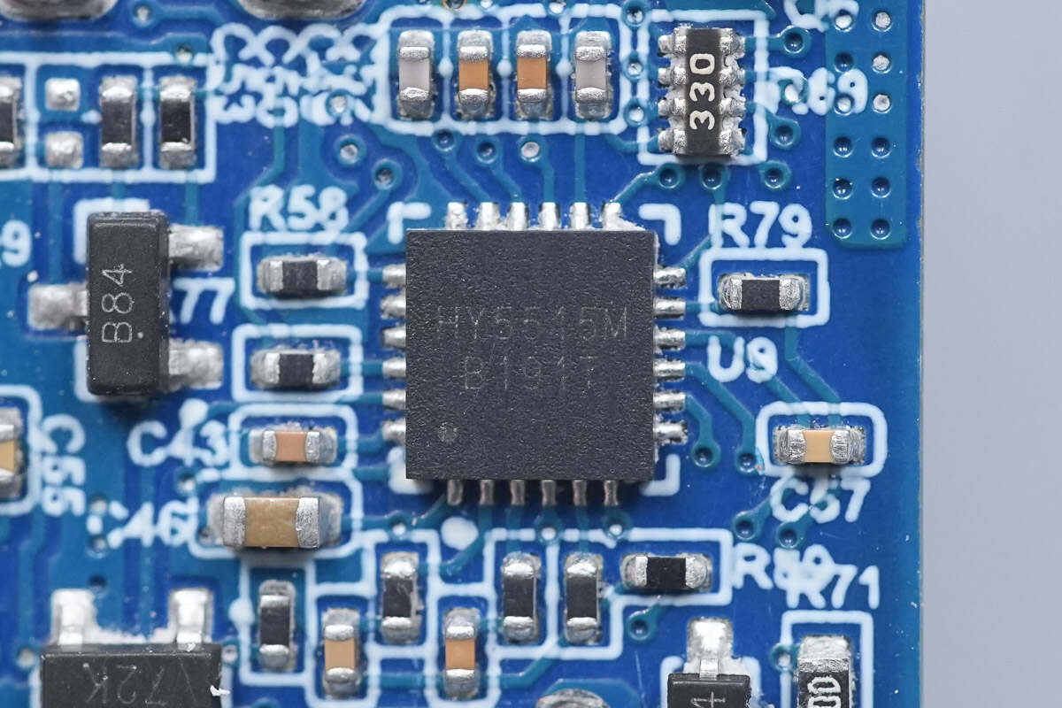
The protocol chip for the other USB-A and USB-C ports also uses the HYASiC HY5515M.
Close-up of the thermistor.
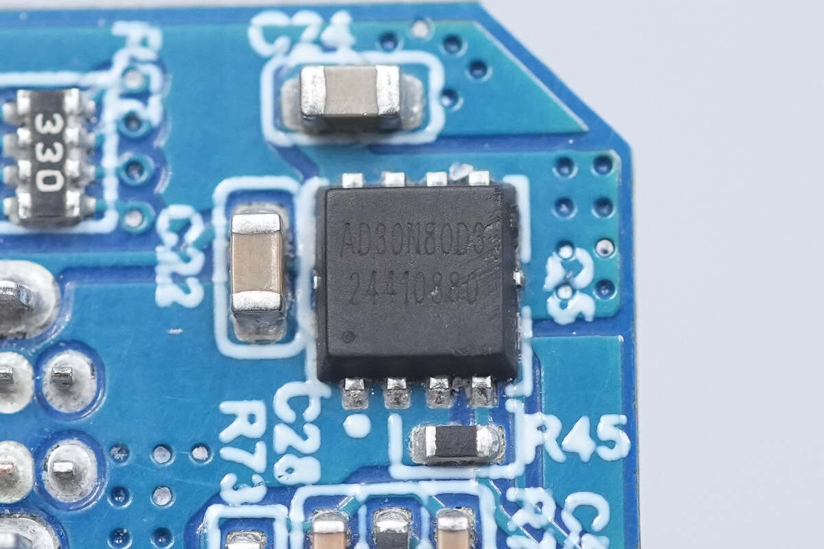
The USB-C1 output VBUS MOSFET is from ADAMANT, model AD30N80D3. It is rated at 30 V with an on-resistance of 3.8 mΩ and comes in a PPAK 3×3 package.
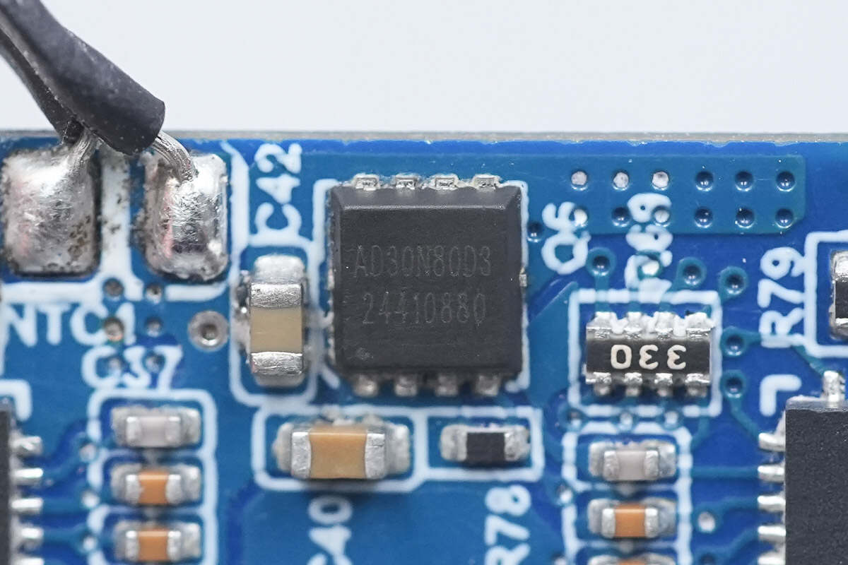
The USB-C2 output VBUS MOSFET also uses the ADAMANT AD30N80D3.
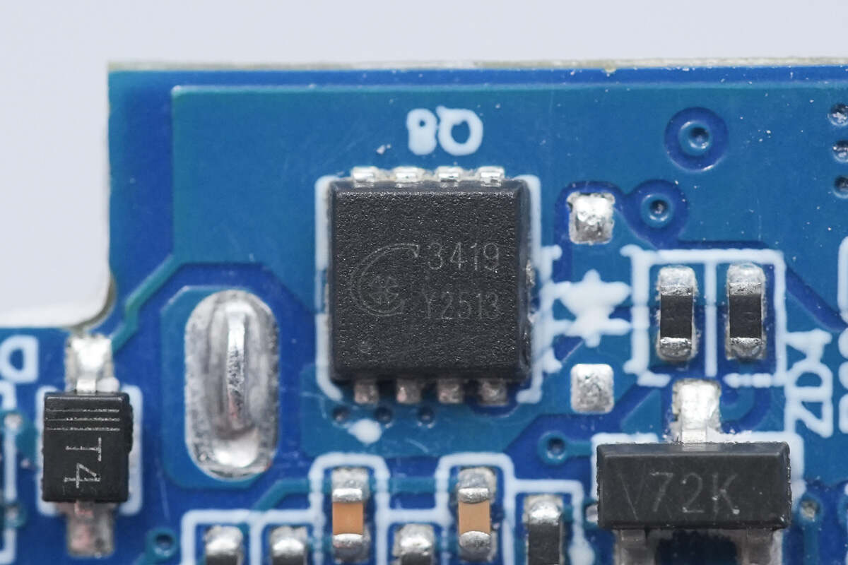
The output VBUS MOSFET is from CXW, model CX3419. It is a P‑channel MOSFET with a voltage rating of 30 V and an on-resistance of 9 mΩ, packaged in a 3×3 mm DFN.
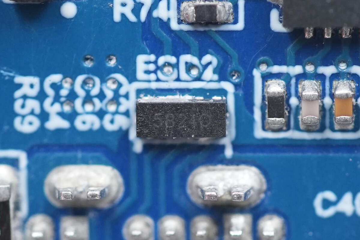
The ESD protection device comes from Goaltop, model GESD5B244JDO. It is housed in a compact DFN2510 package measuring just 2.5 × 1.0 × 0.5 mm and integrates four ESD protection channels. It features a dual-channel design with 5 V bidirectional and 24 V unidirectional protection, providing precise pass-through protection for the D+, D-, and CC lines of PD USB-C interfaces.
This clever design offers comprehensive ESD protection for USB-C signal channels such as D+, D-, CC1, and CC2, while greatly simplifying PCB routing. The integrated design also reduces component cost and SMT assembly steps, improving overall cost-effectiveness.
To meet PD 3.0 20 V requirements, it provides two 5 V and two 24 V working voltage channels, with excellent low capacitance and fast response, ensuring rapid dissipation of electrostatic energy to protect devices from ESD damage. It also features extremely low leakage current and high reliability.

Close-up of another Goaltop GESD5B244JDO ESD protection device.
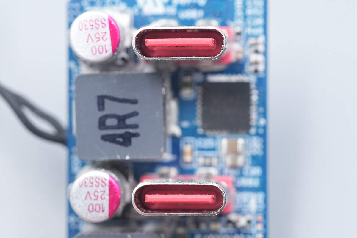
Close-up of the USB-C sockets.
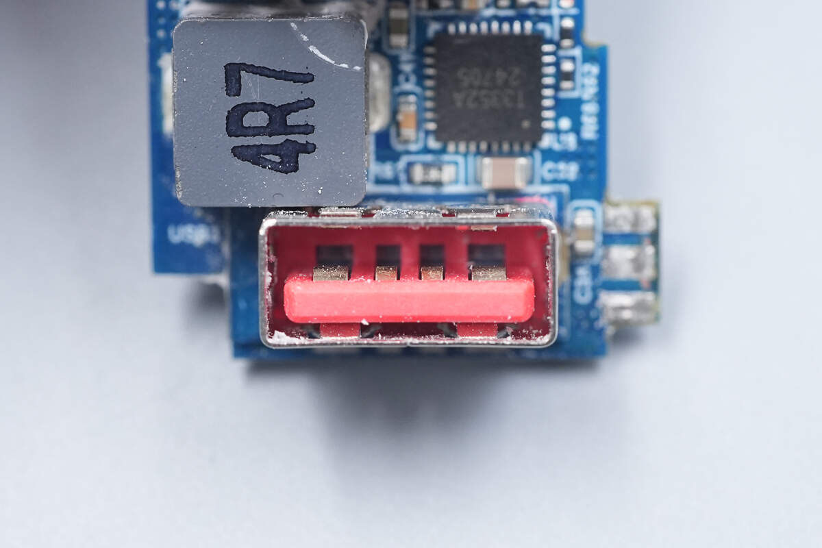
Close-up of the USB-A socket.

Well, those are all components of the ASUS Adol 100W GaN Quick Charger.
Summary of ChargerLAB

Here is the component list of the ASUS Adol 100W GaN Quick Charger for your convenience.
It is available in five color options. The product features a thoughtfully designed compact body with foldable pins, making it convenient for portability.
After taking it apart, we found that thanks to the HYASiC HY5515M fast-charging solution, both USB-C ports support 100 W output. They are compatible with UFCS, PD 3.0, SCP, and Xiaomi’s 90 W proprietary fast-charging protocols.
The power supply uses an efficient PFC+AHB topology, combining the X-Signal PFC controller XP3323 with the DONGKE DK8710BD integrated GaN chip solution, ensuring improved efficiency and system reliability. It uses an encapsulation process to enhance overall thermal performance and drop resistance, with high-quality materials and reliable workmanship.
Related Articles:
1. Teardown of CUKTECH 15 Charging Station (TA1406U)
2. Teardown of Xiaomi 45W GaN Pudding Charger (MDY-18-EZ)
3. Teardown of Anker Nano 45W GaN Charger with Display (A121D)