Introduction
In 2021, Apple launched the industry’s first 140W PD 3.1 GaN charger, model A2452, which not only pioneered a new fast-charging market but also helped drive the entire fast-charging industry toward higher voltages and greater power. Five years later, Apple has introduced a new version of this 140W charger, model A3607.
While the exterior, dimensions and specifications remain largely unchanged from the previous version, questions arise regarding whether the internal architecture has been modified and whether the core components have been upgraded. To address these questions, we conducted a teardown of the A3607 to reveal its internal design.
Product Appearance
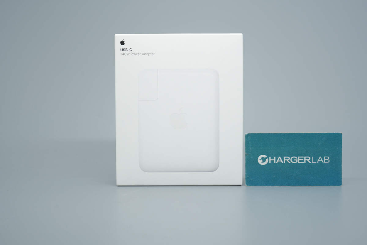
The front of the packaging features the Apple logo, the product name, and an image of the charger.
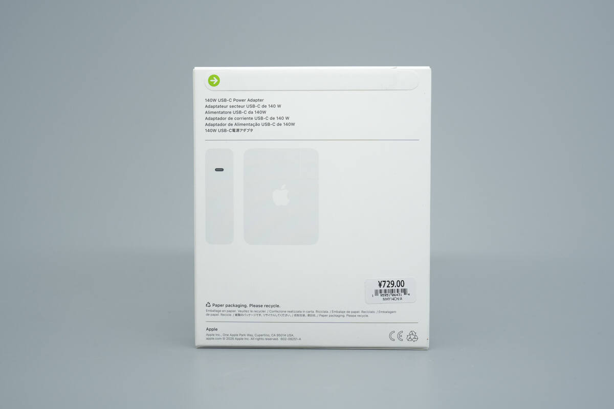
The back of the packaging displays a schematic of the charger along with certification marks and other relevant information.
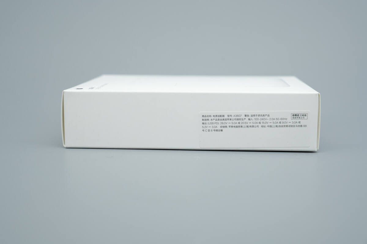
A specification label is affixed to the side of the packaging.
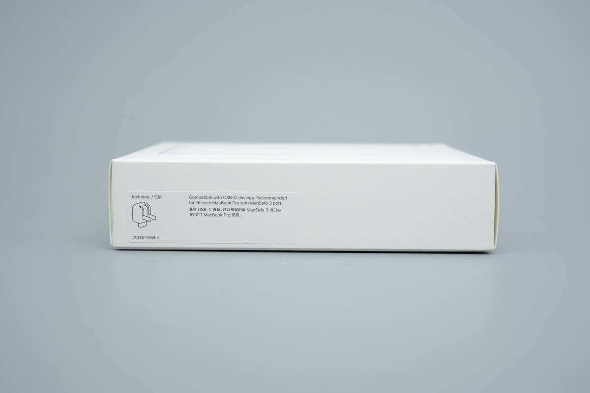
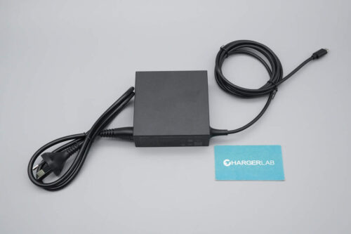
The charger is compatible with USB-C devices, with Apple officially recommending its use alongside the 16-inch MacBook Pro equipped with a MagSafe 3 port.
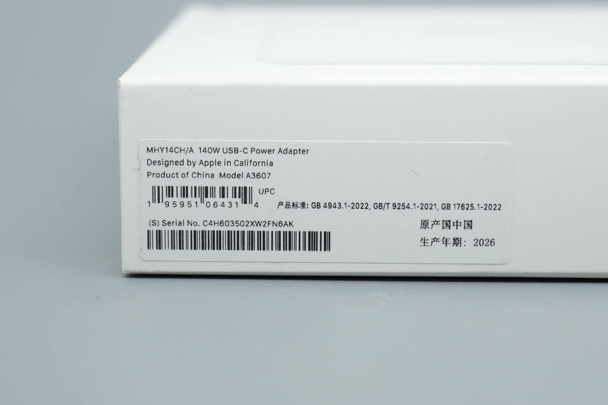
The production date is 2026, and the model number is A3607.
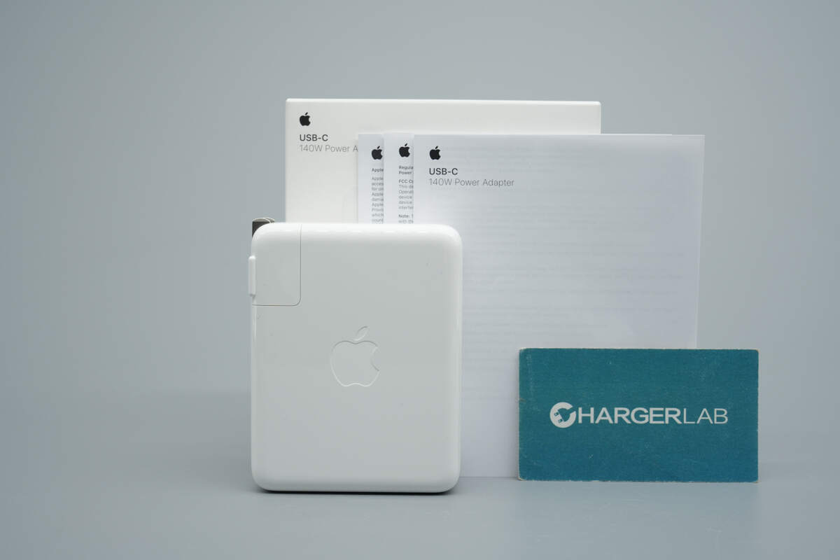
The package includes the charger along with a user manual and related documentation.
The charger is wrapped in a protective film to prevent scratches.
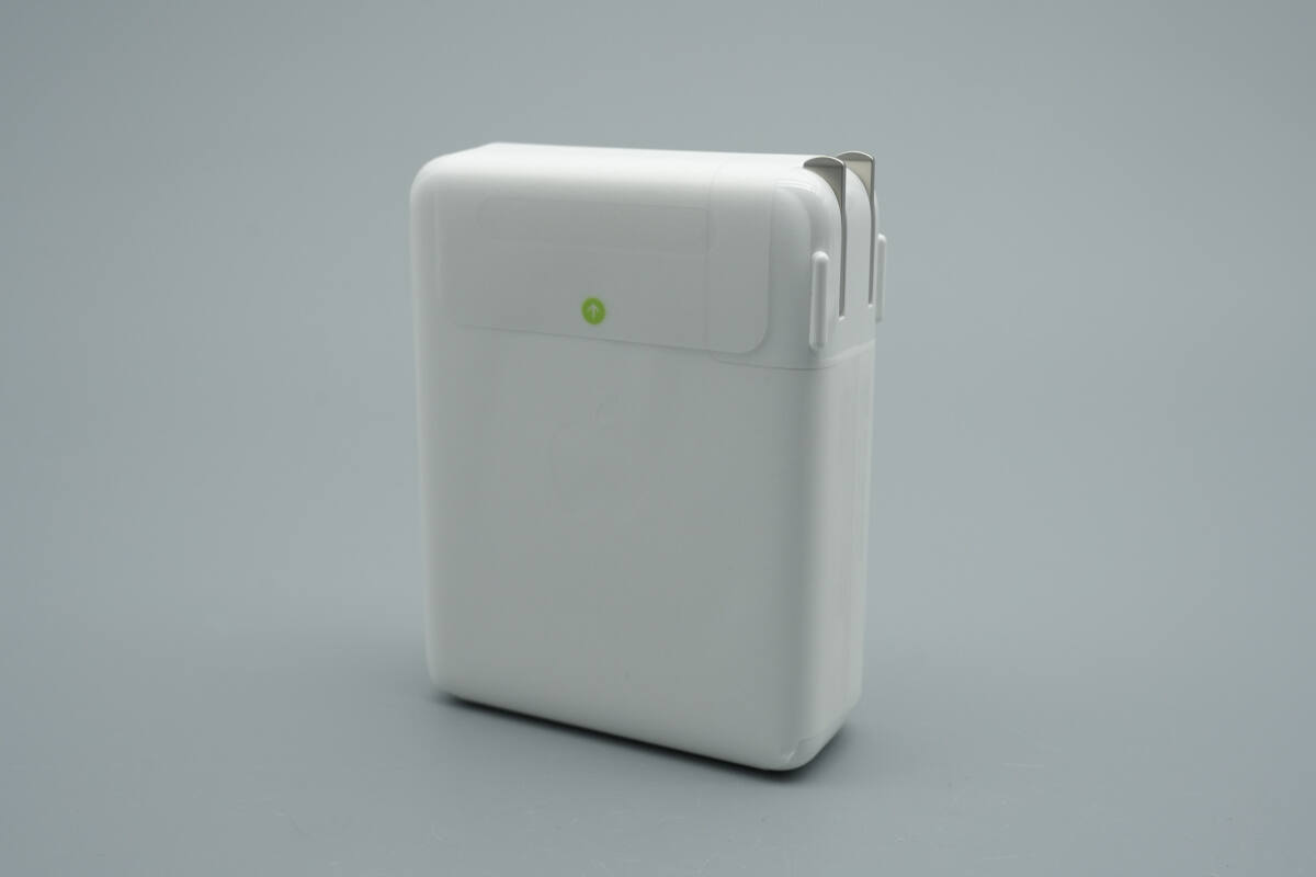
The appearance is identical to the previous version, featuring a glossy finish and smoothly rounded edges.
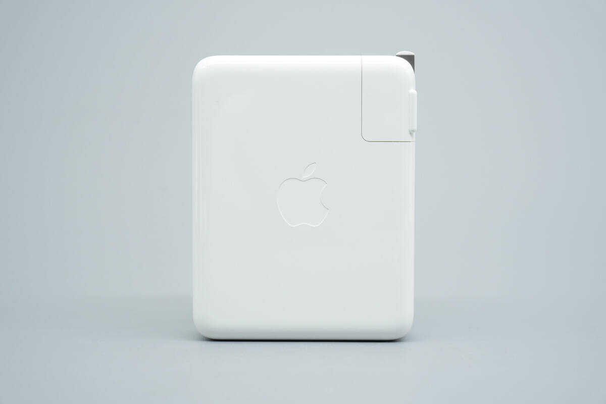
Both the front and back centers feature the Apple logo.
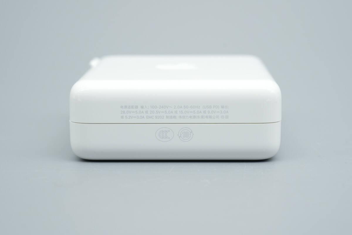
This side displays the technical specifications.
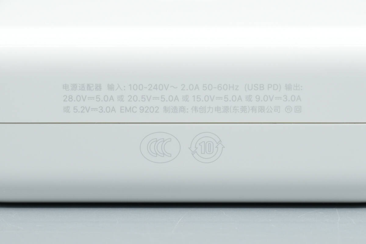
Input: 100–240V ~ 50/60Hz 2A
(USB PD) Output: 5.2V 3A, 9V 3A, 15V 5A, 20.5V 5A, 28V 5A
The charger has passed CCC and KC certifications.
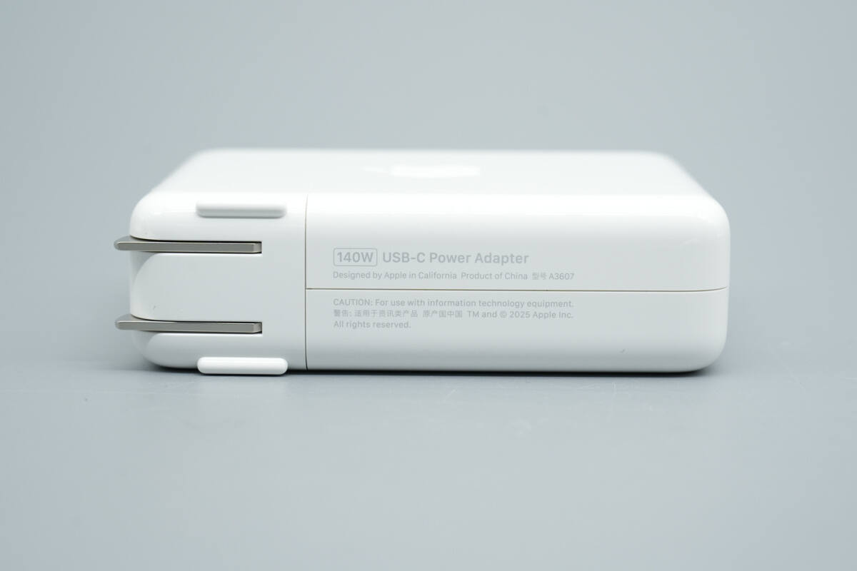
The other side of the casing displays the product name, model number, and safety notices.
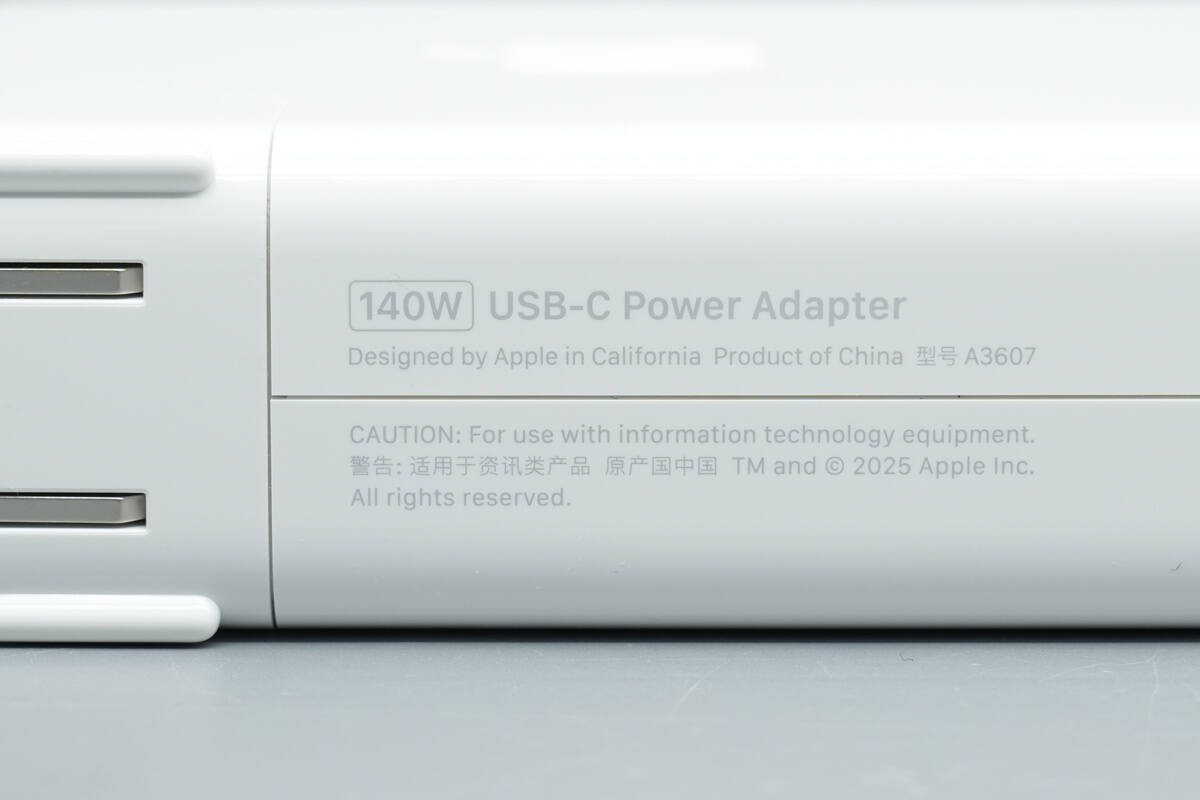
The model is A3607.
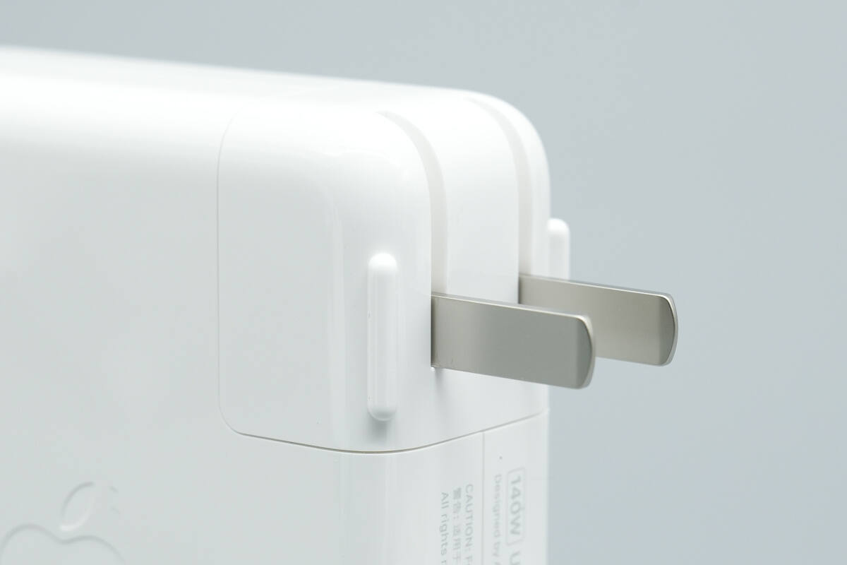
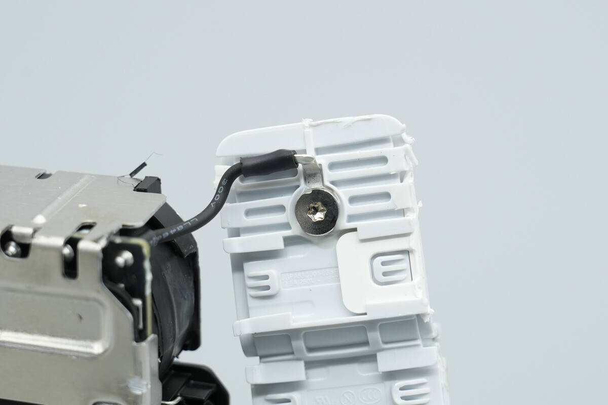
It is equipped with foldable prongs.
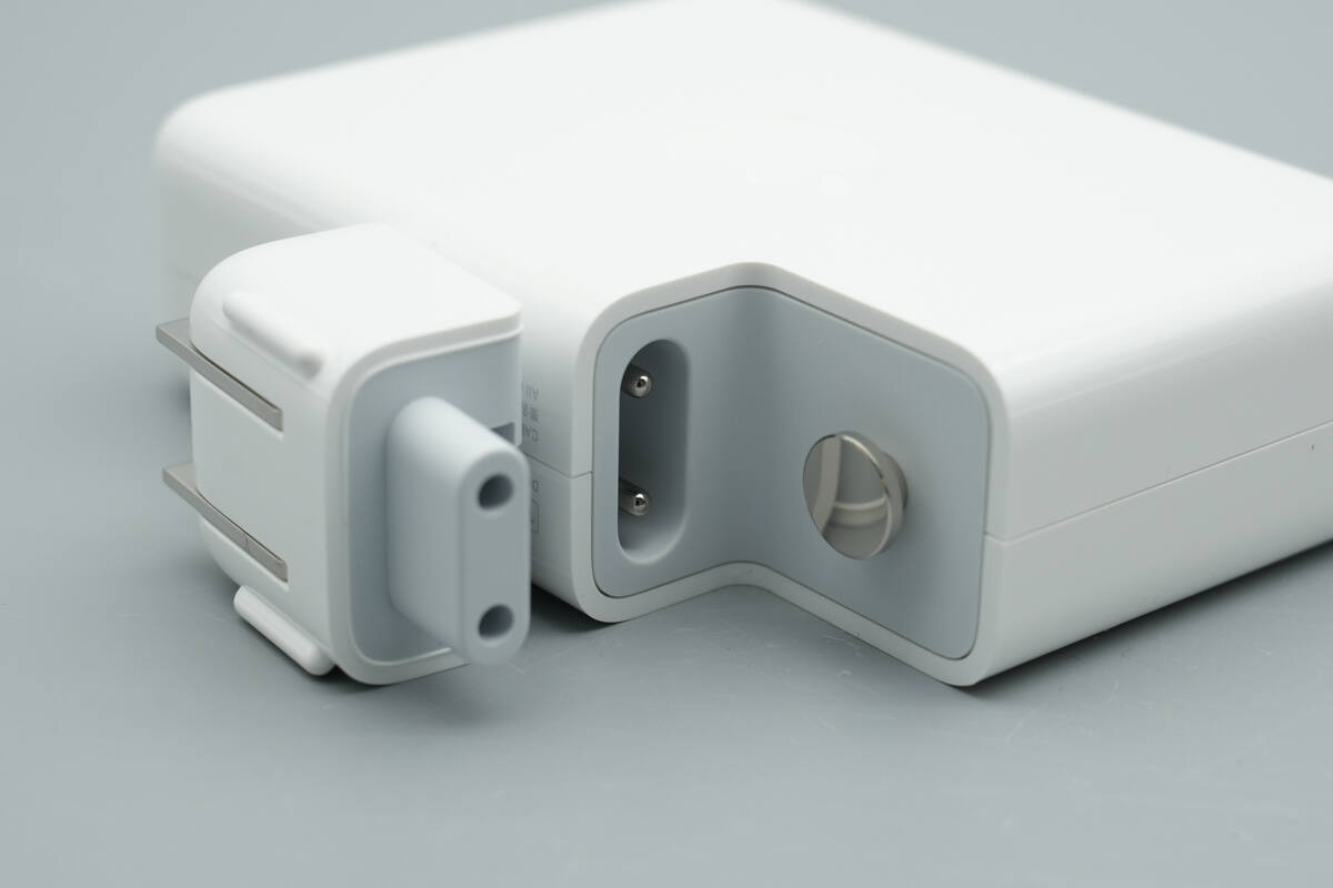
The prongs feature a modular design, allowing them to be detached and replaced.
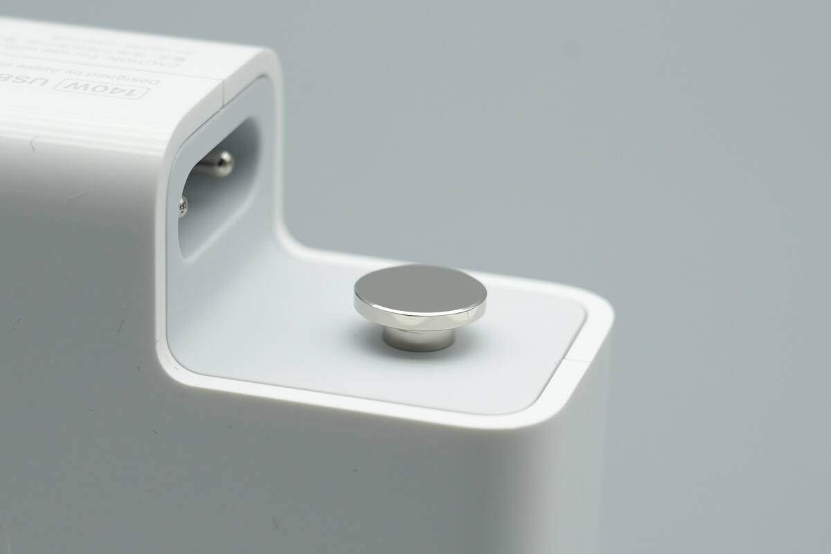
Close-up of the mounting base, which can also serve as a grounding point.
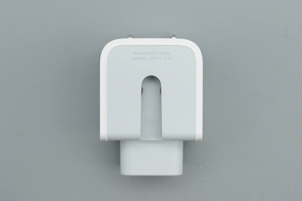
The prong module casing is marked with 250V ~ 2.5A and Jabil Inc., indicating that the prong module is supplied by Jabil. Notably, the module slot now includes a metal clip for additional securing, ensuring that the module remains firmly in place during long-term use.
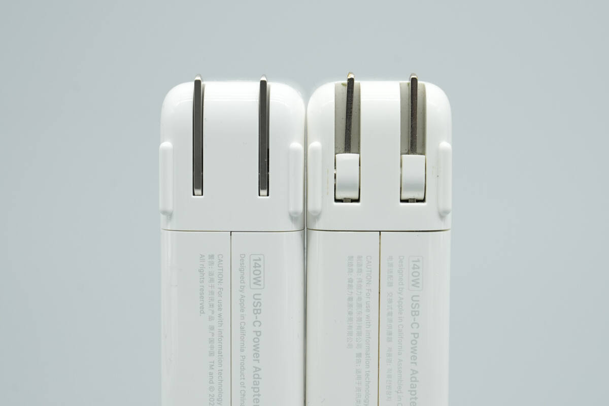
Compared with the previous version, the prong design has also been modified.
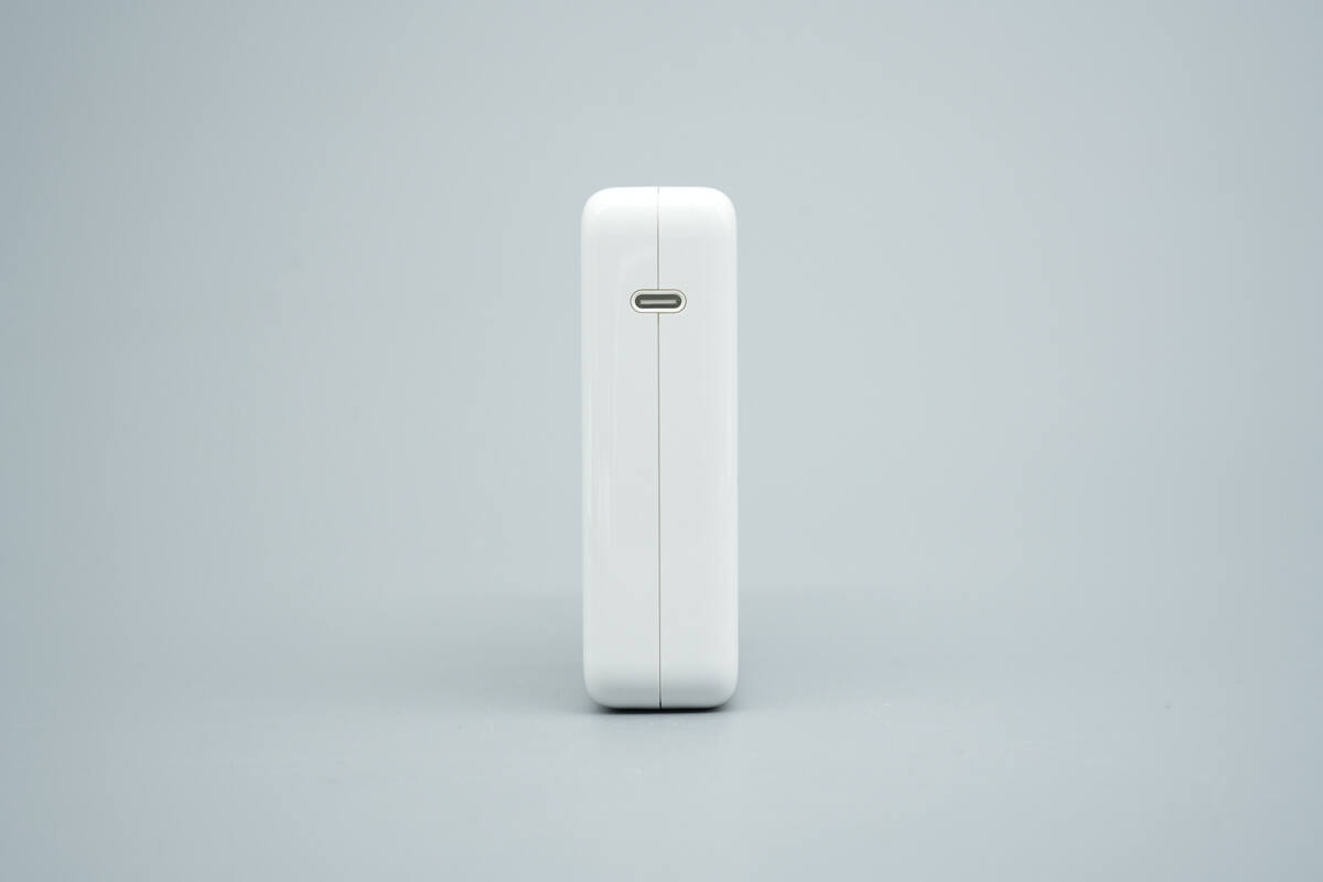
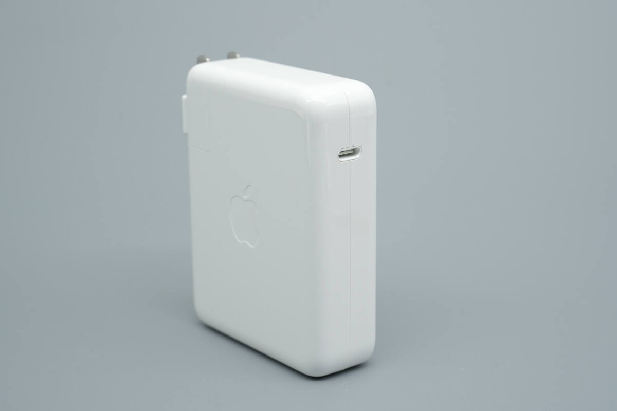
The output side features a single USB-C port with a white plastic sheet.
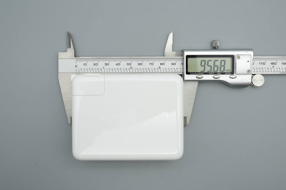
The length of the charger is about 95.68 mm (3.77 inches).
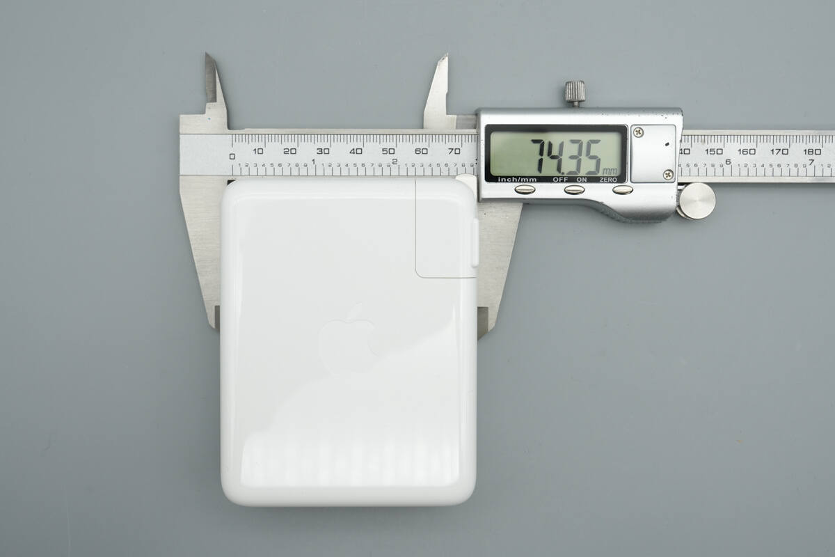
The width is about 74.35 mm (2.93 inches).
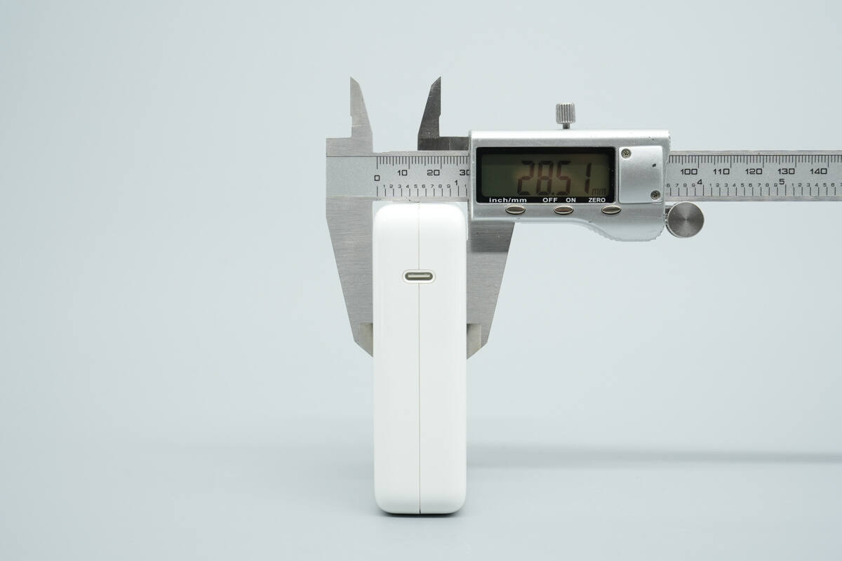
The thickness is about 28.51 mm (1.12 inches).
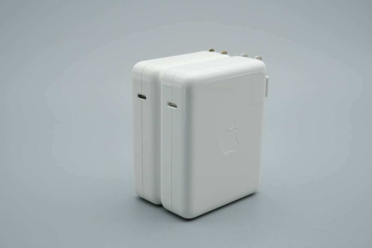
When compared side by side with Apple’s previous 140W GaN charger, model A2452, the main body and dimensions of the new and old versions are identical.
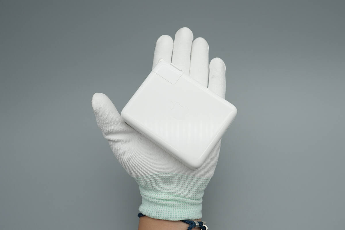
That's how big it is in the hand.
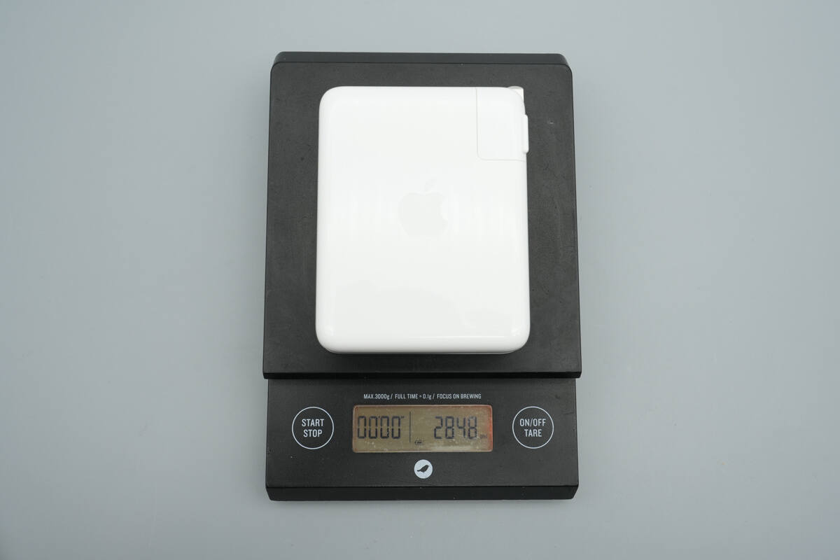
The weight is about 285 g (10.053 oz).
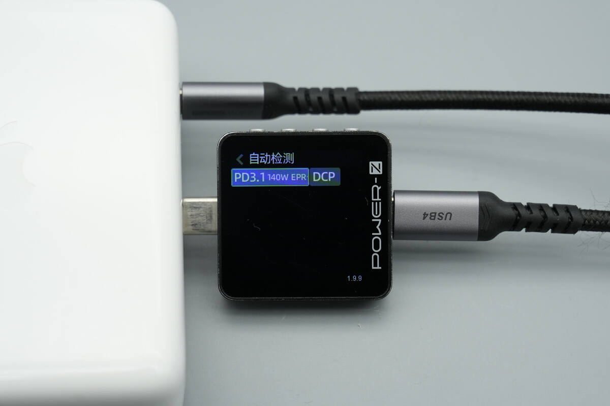
ChargerLAB POWER-Z KM003C shows that the USB-C supports PD3.1 and DCP charging protocols.
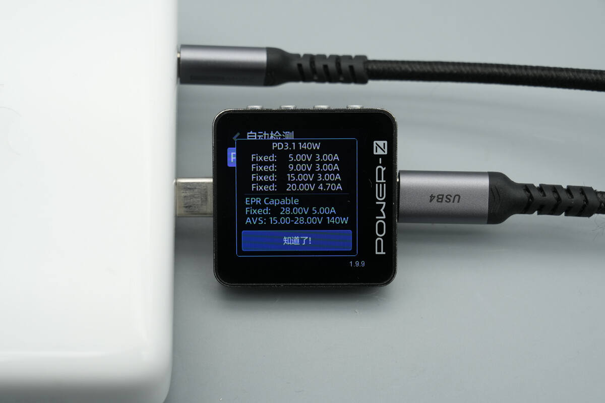
It features five fixed PDOs: 5V 3A, 9V 3A, 15V 3A, 20V 4.7A, and 28V 5A, as well as a 15–28V 140W AVS voltage range.
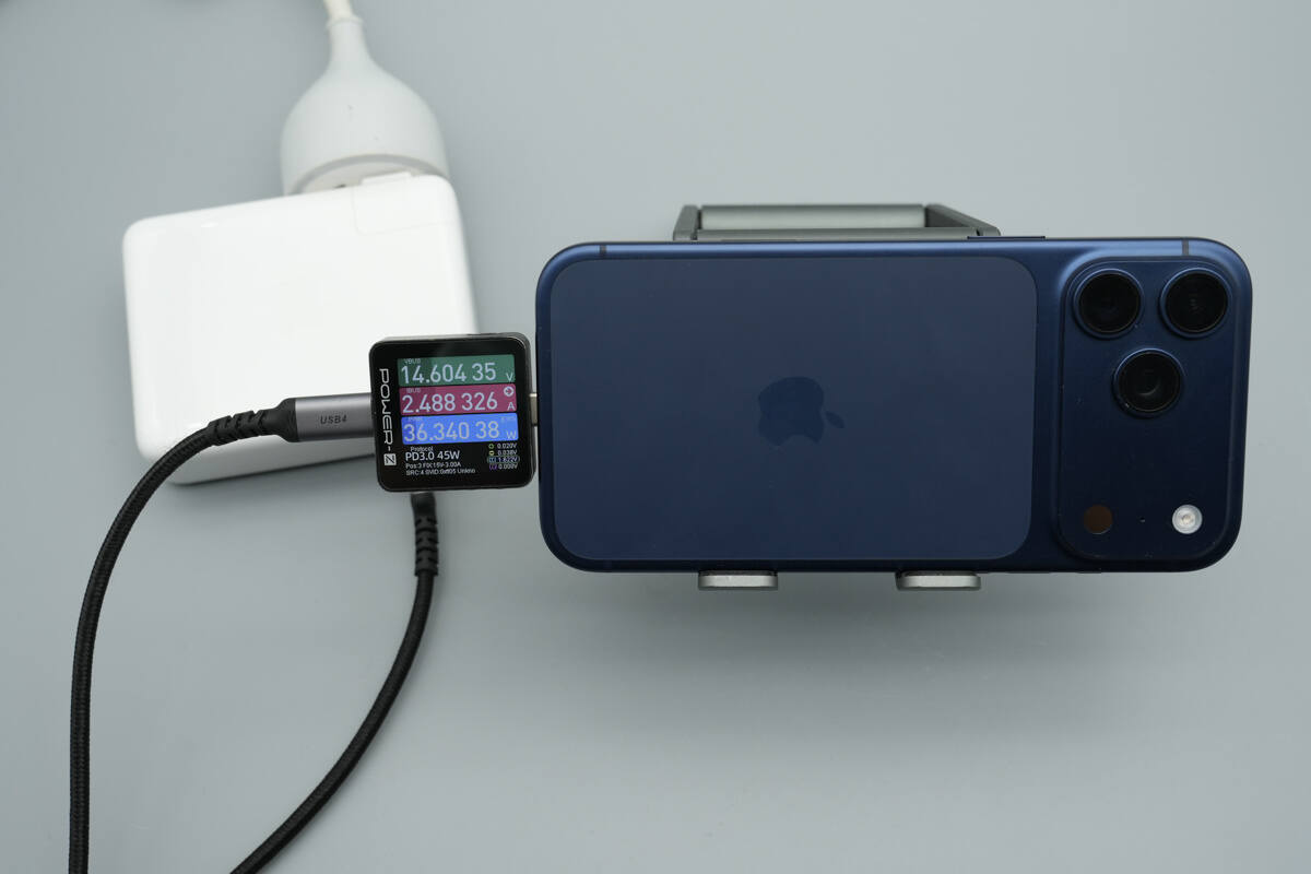
Use it to charge the iPhone 17 Pro Max, the power is about 36.34W.
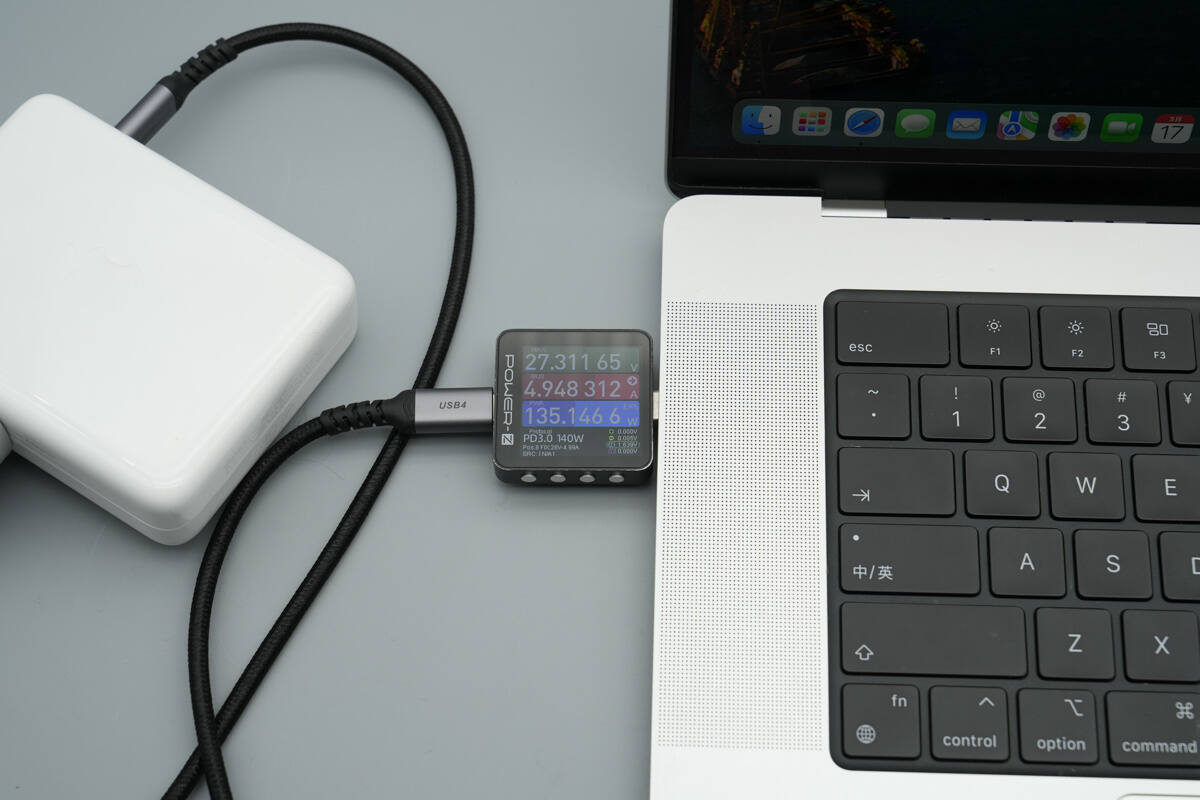
Use it to charge the MacBook Pro, the power is about 135.15W, successfully enabling 28V 5A 140W fast charging.
Teardown
Next, let's take it apart to see its internal components and structure.
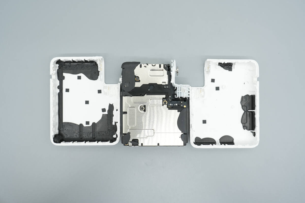
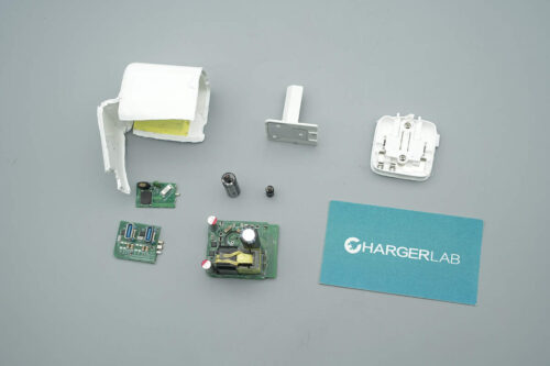
Cut along the side to open the casing.
The casing is thick, with adhesive applied along the edges to reinforce the module.
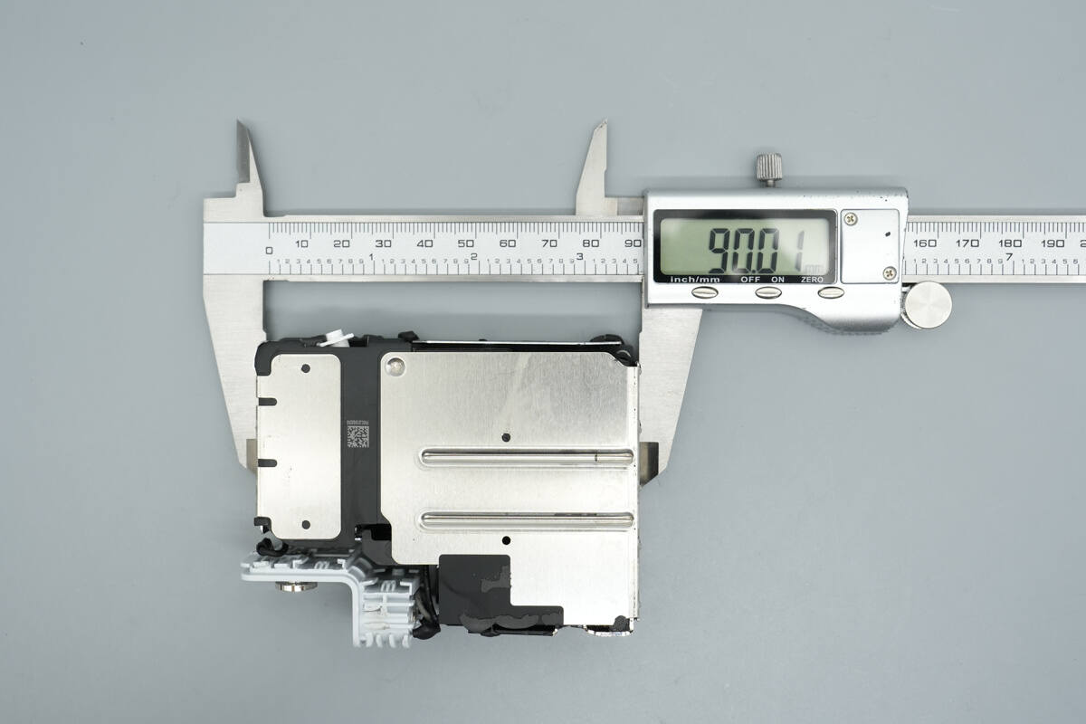
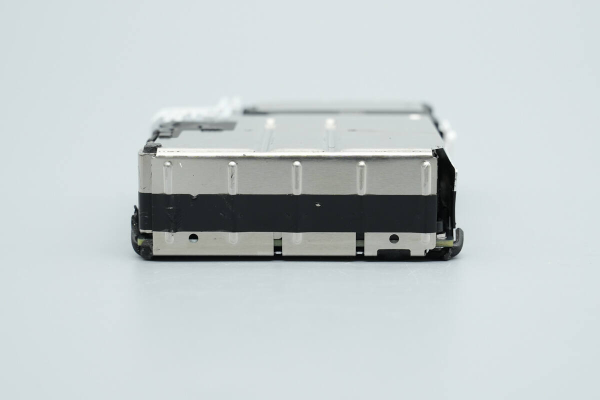
The length of the PCBA module is about 90.01 mm (10.053 inches).
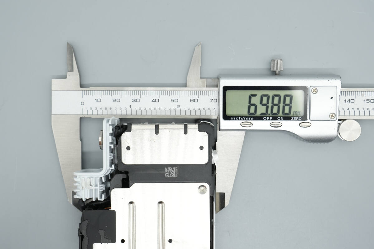
The width is about 69.88 mm (2.75 inches).
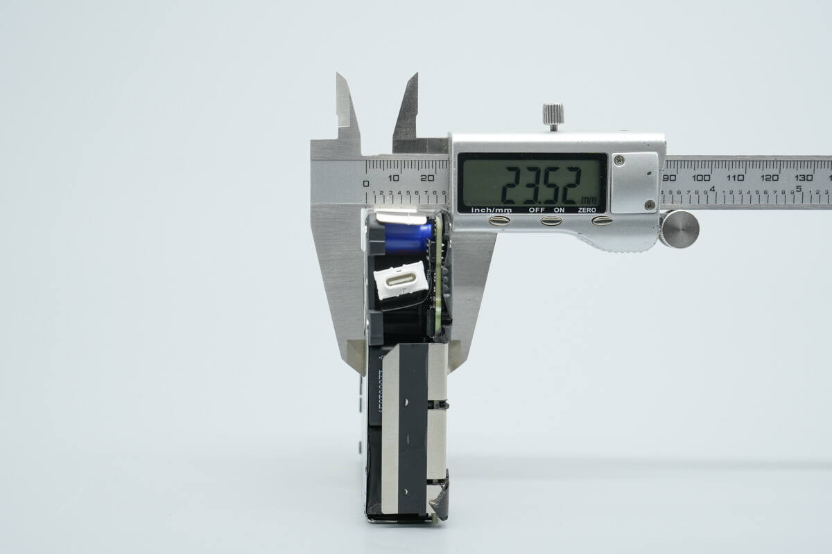
The thickness is about 23.52 mm (0.93 inches).
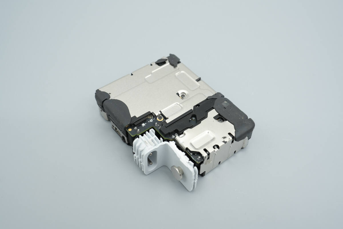
The PCBA module is enclosed by two integrated metal shells for uniform heat dissipation.
The metal shells are secured with screws.
Insulating tape is applied to the side area.
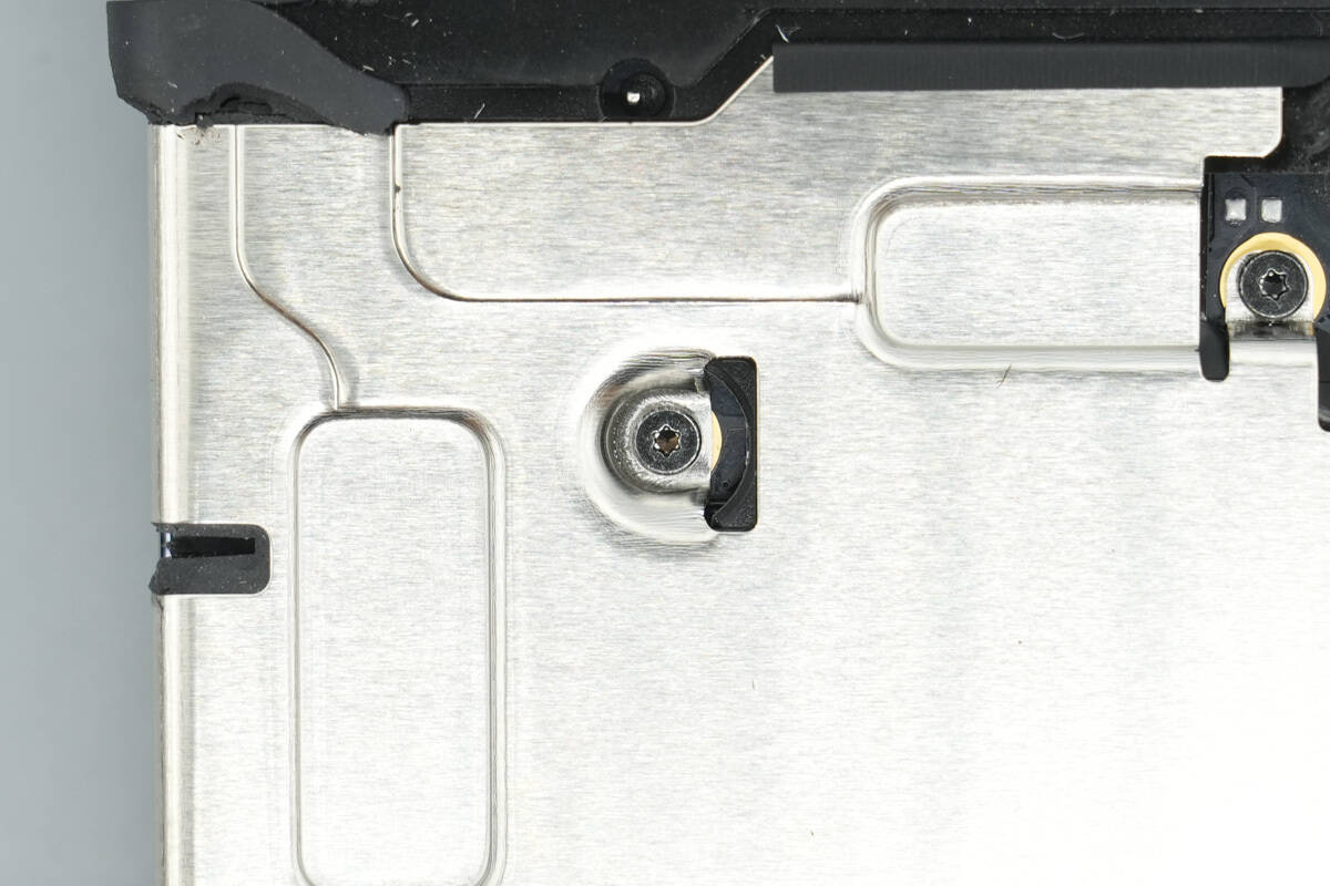
A wire from the input side is connected to the T-shaped mounting base for grounding.
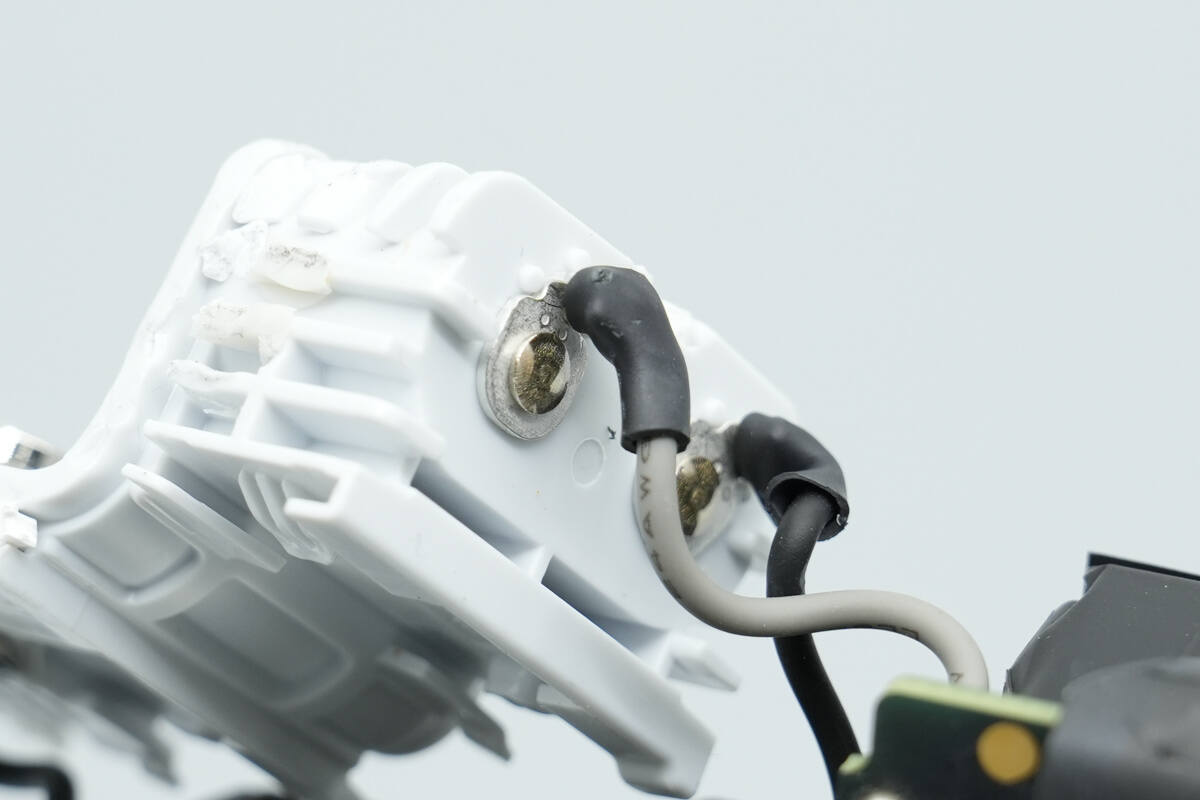
The soldered connections of the AC wire terminals are insulated with heat-shrink tubing.
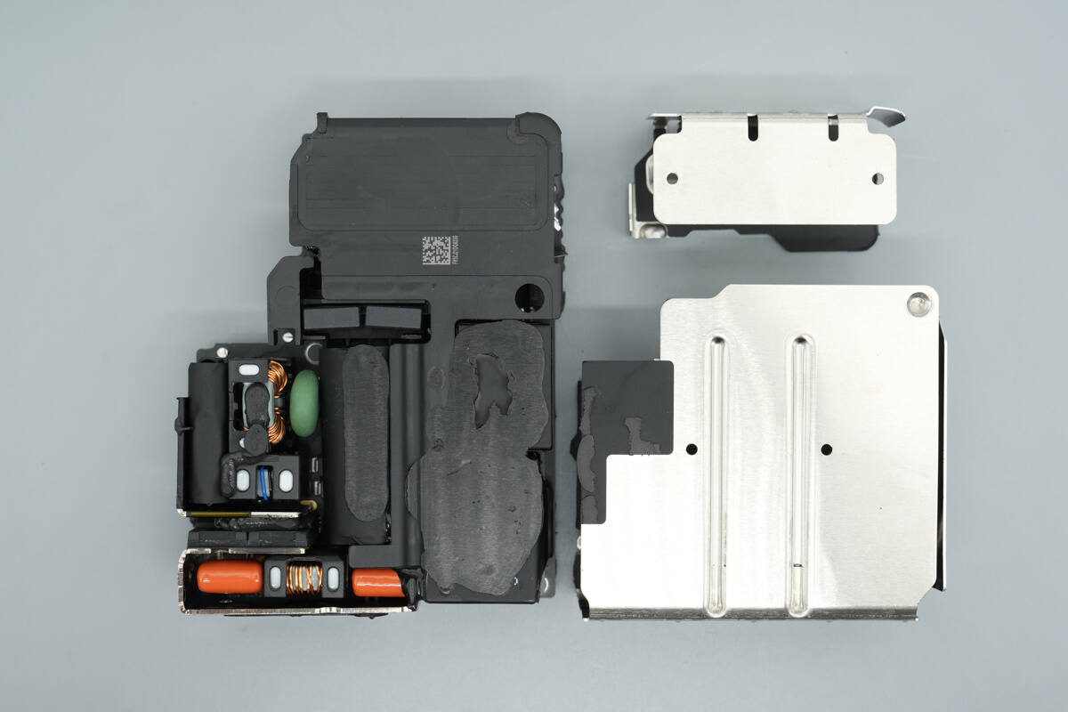
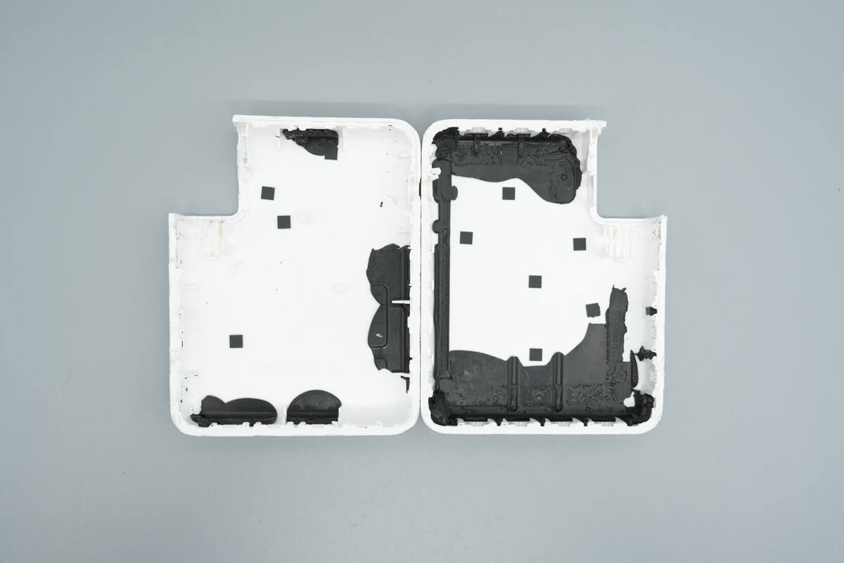
Remove the metal casings.
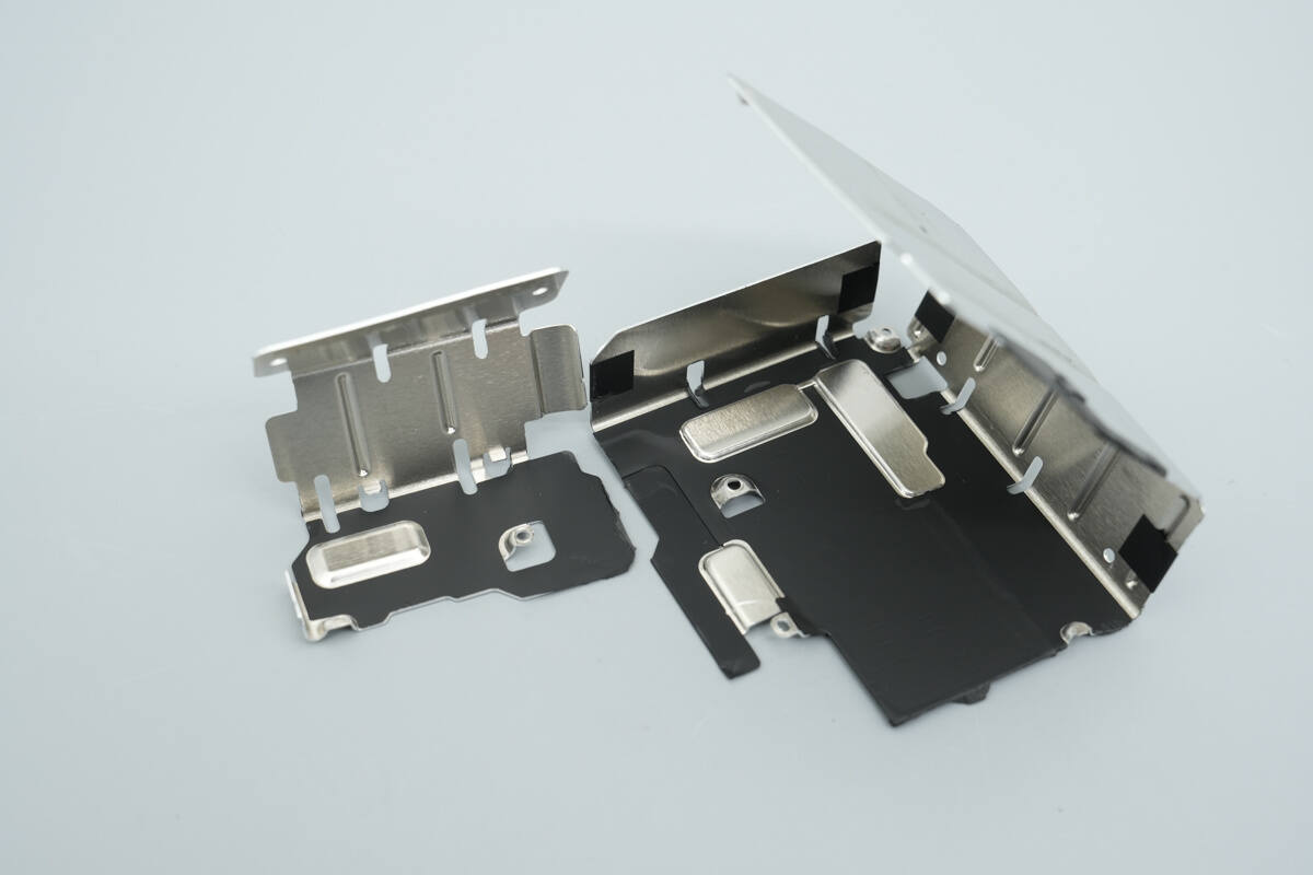
The inner side of the metal casing is insulated.
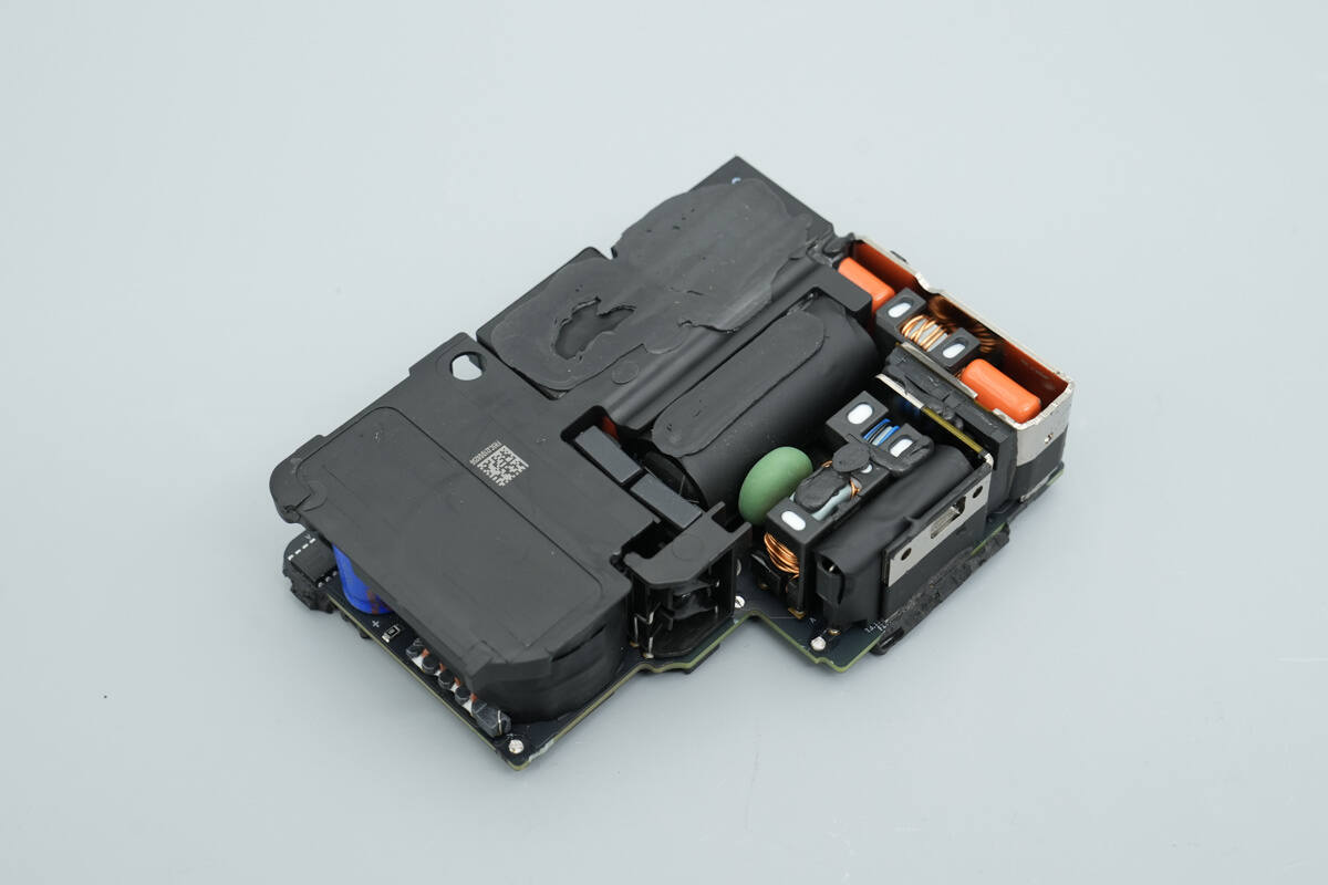
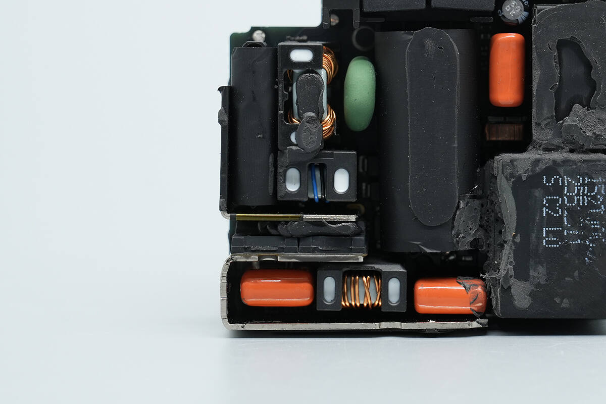
A plastic cover is placed over the transformer area of the module.
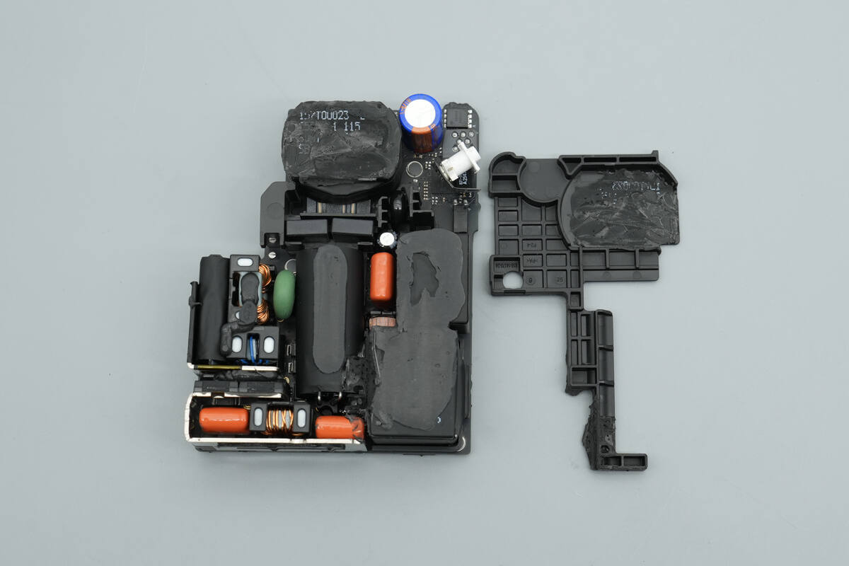
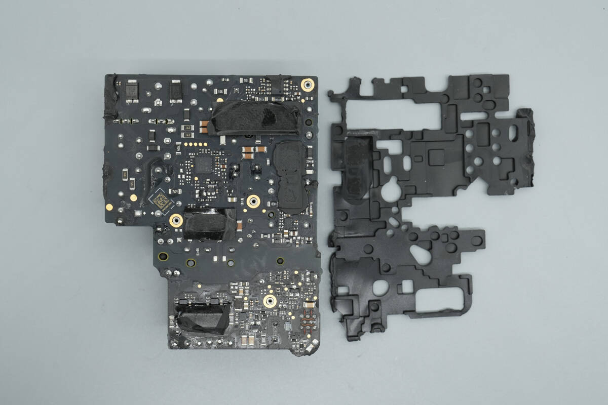
After removing the plastic cover, a plastic frame is revealed in the center of the module.
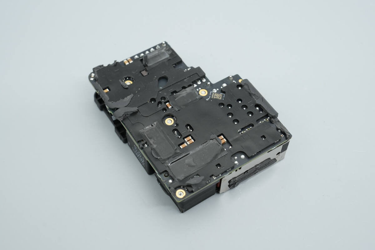
The back of the module is covered with a soft rubber pad.
After removing the protective pad, thermal paste is applied to the chip areas, and graphite thermal sheets are attached.
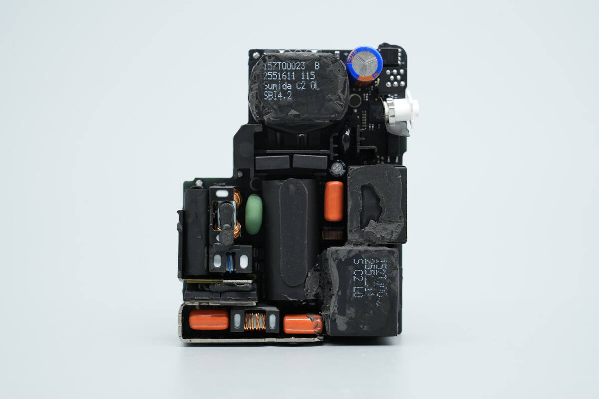
The front of the PCBA module features components including a fuse, common mode chokes, high-voltage filter electrolytic capacitors, a current transformer, film capacitors, a PFC boost inductor, a buck inductor, and a transformer.
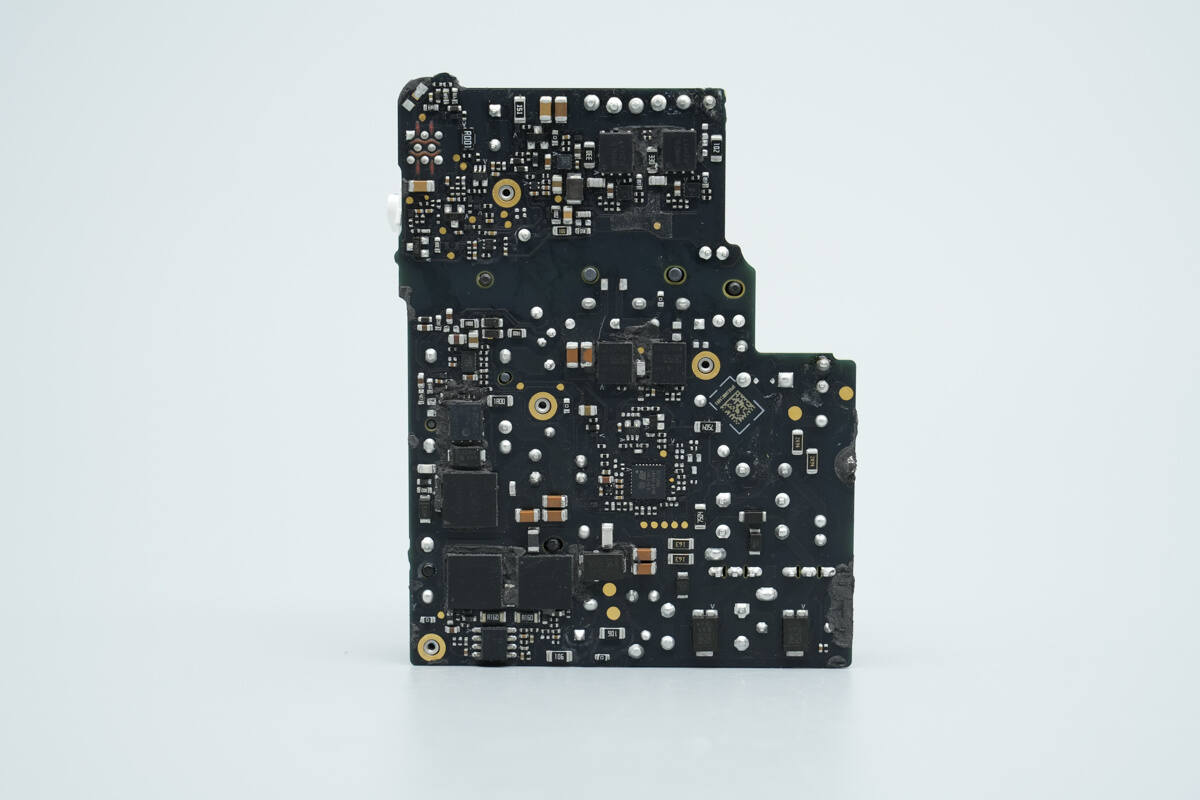
The back of the PCB houses the controllers for the PFC boost circuit and the LLC circuit, as well as MOSFETs and other related components.
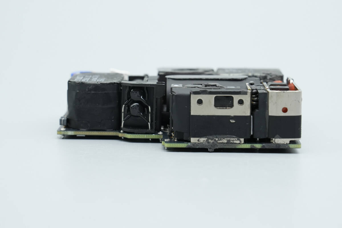
There are two heat sinks at the module’s input side.
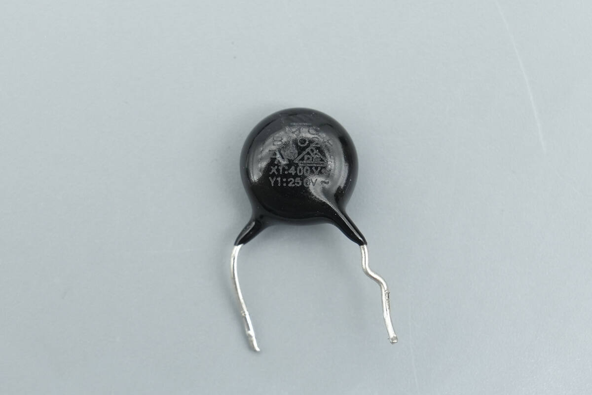
Within the area enclosed by the two heat sinks, there are a fuse, a safety X2 capacitor, common-mode chokes, a varistor, film capacitors, a filter inductor, and other components.
The fuse is positioned on top of the safety X2 capacitor and is wrapped with tape.
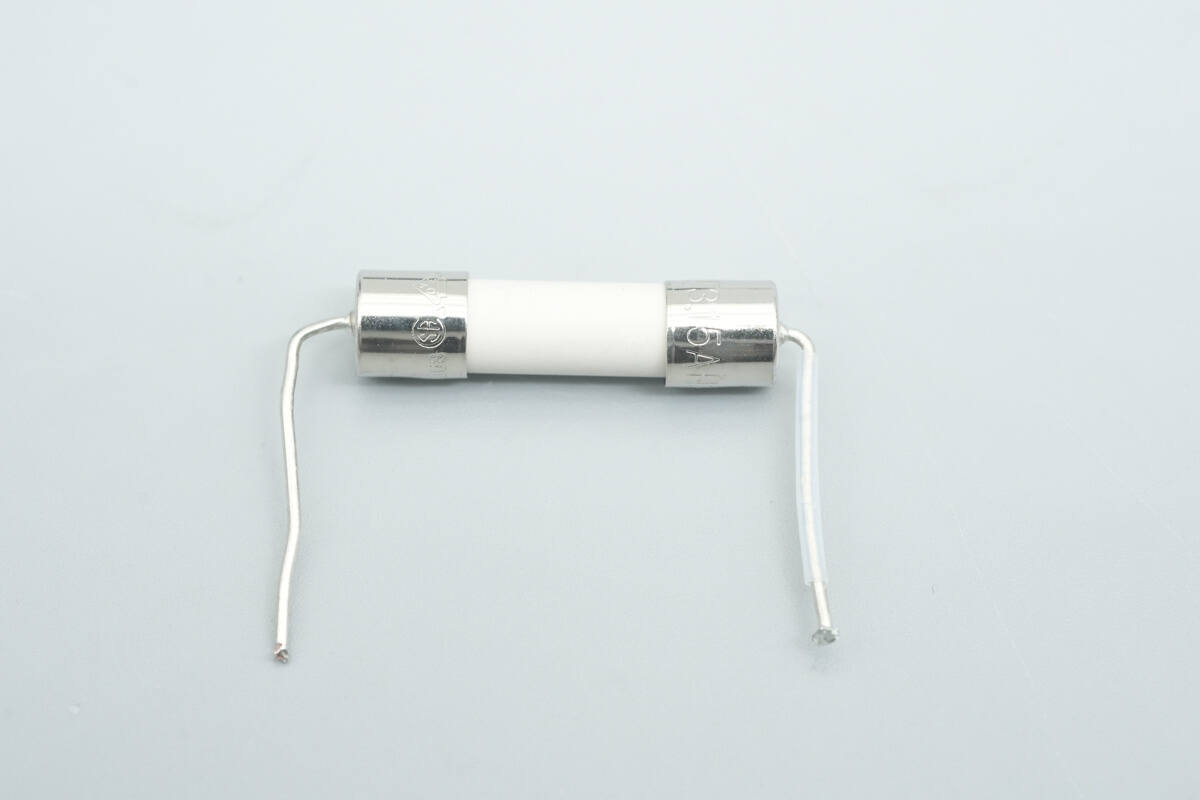
The fuse is rated at 3.15A.
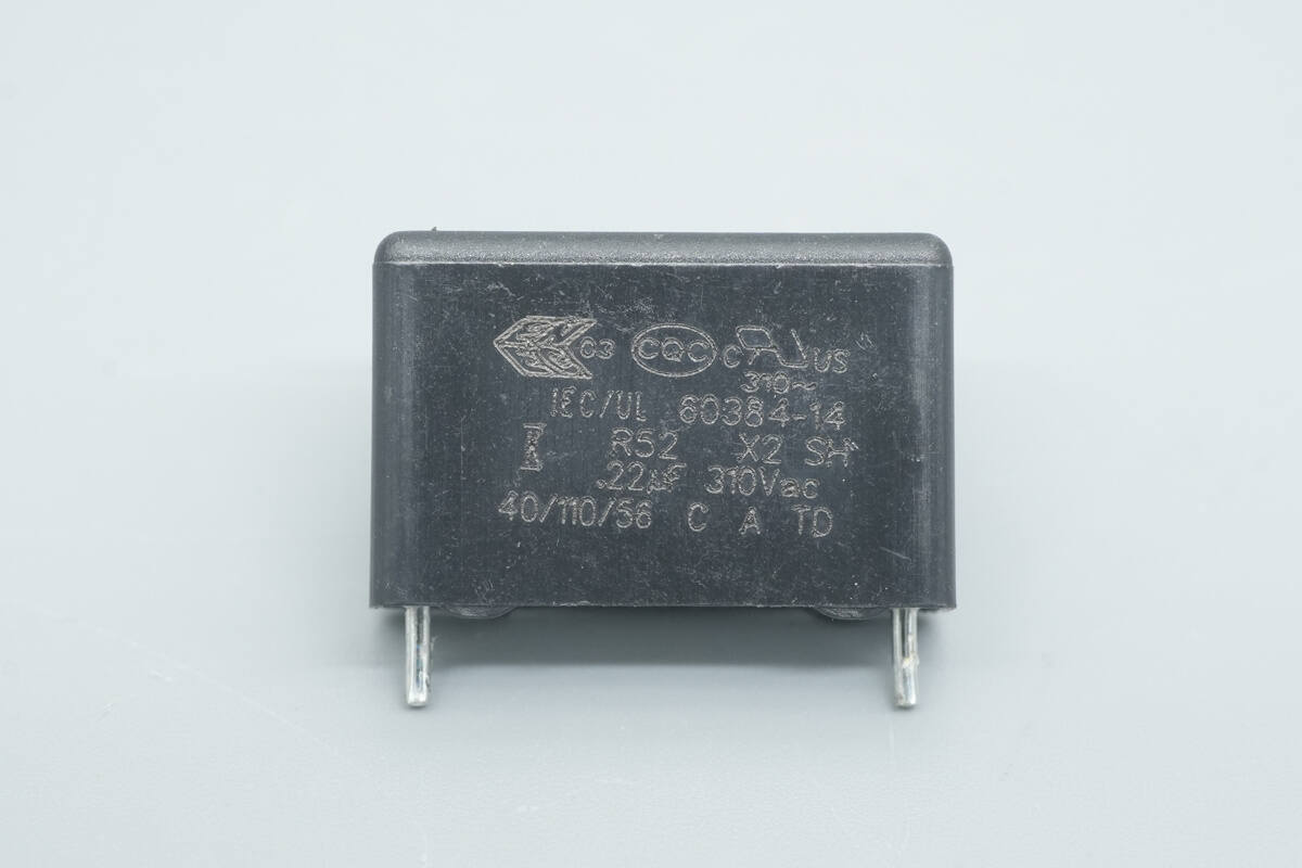
The safety X2 capacitor has a capacitance of 0.22 μF.
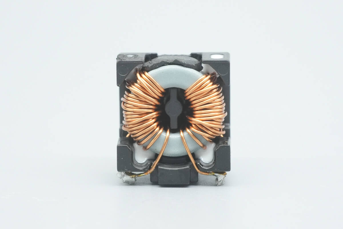
The common mode choke is used to filter EMI interference and is soldered with a plastic housing.
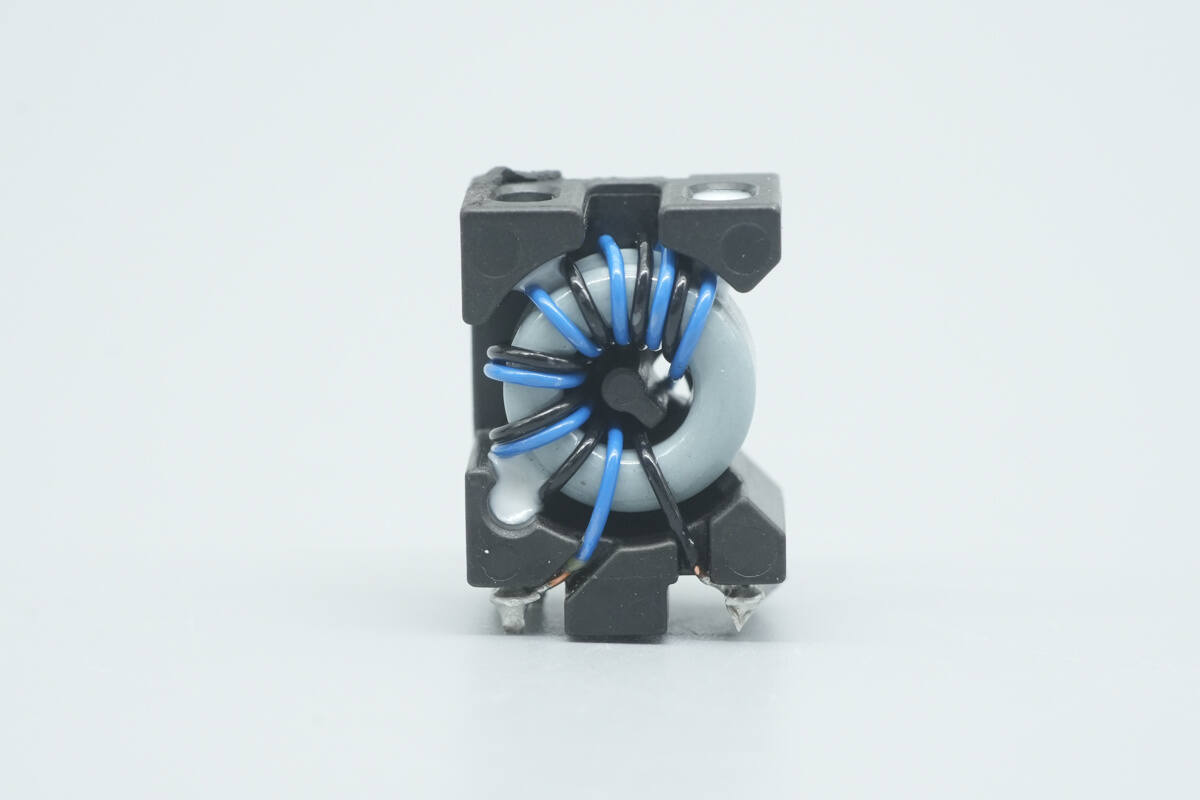
Close-up of another common mode choke.
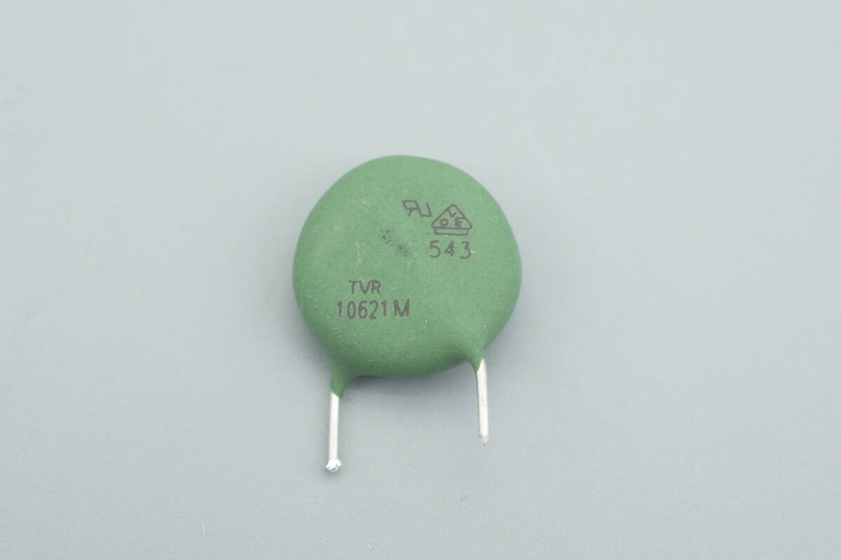
A TVR10621M varistor, used for input overvoltage protection.
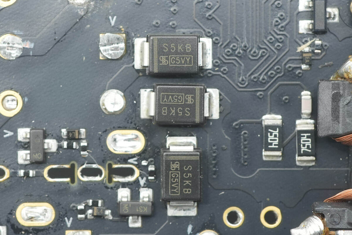
The input stage uses four diodes arranged in a bridge rectifier configuration.
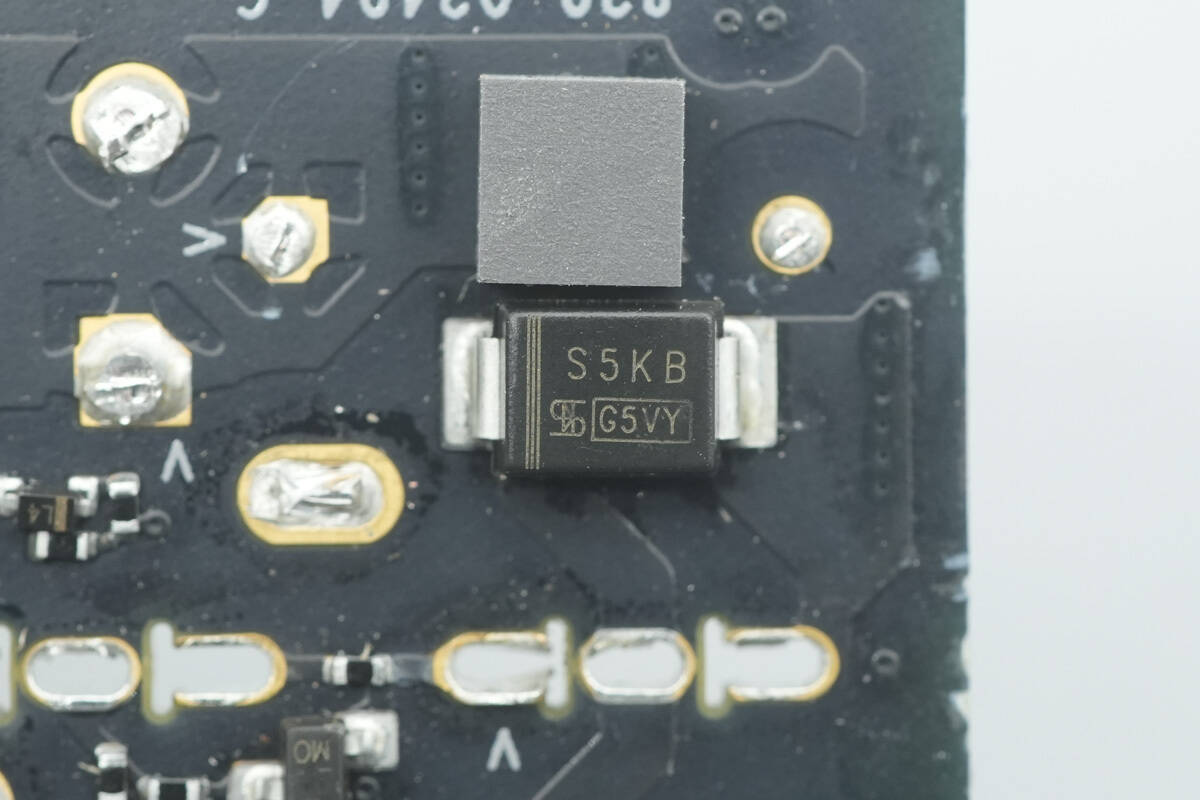
Close-up of the fourth diode.
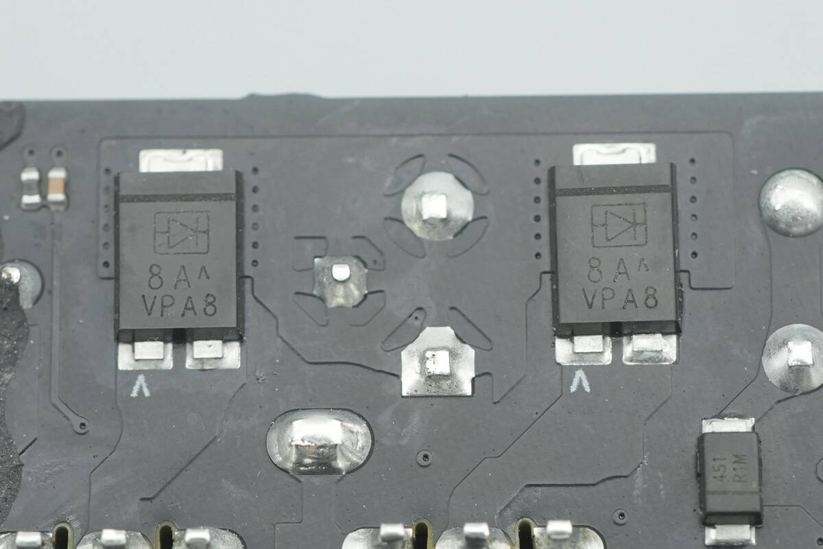
Close-up of the other two diodes, paired with the Infineon CoolMOS IPA65R095C7 for active rectification.
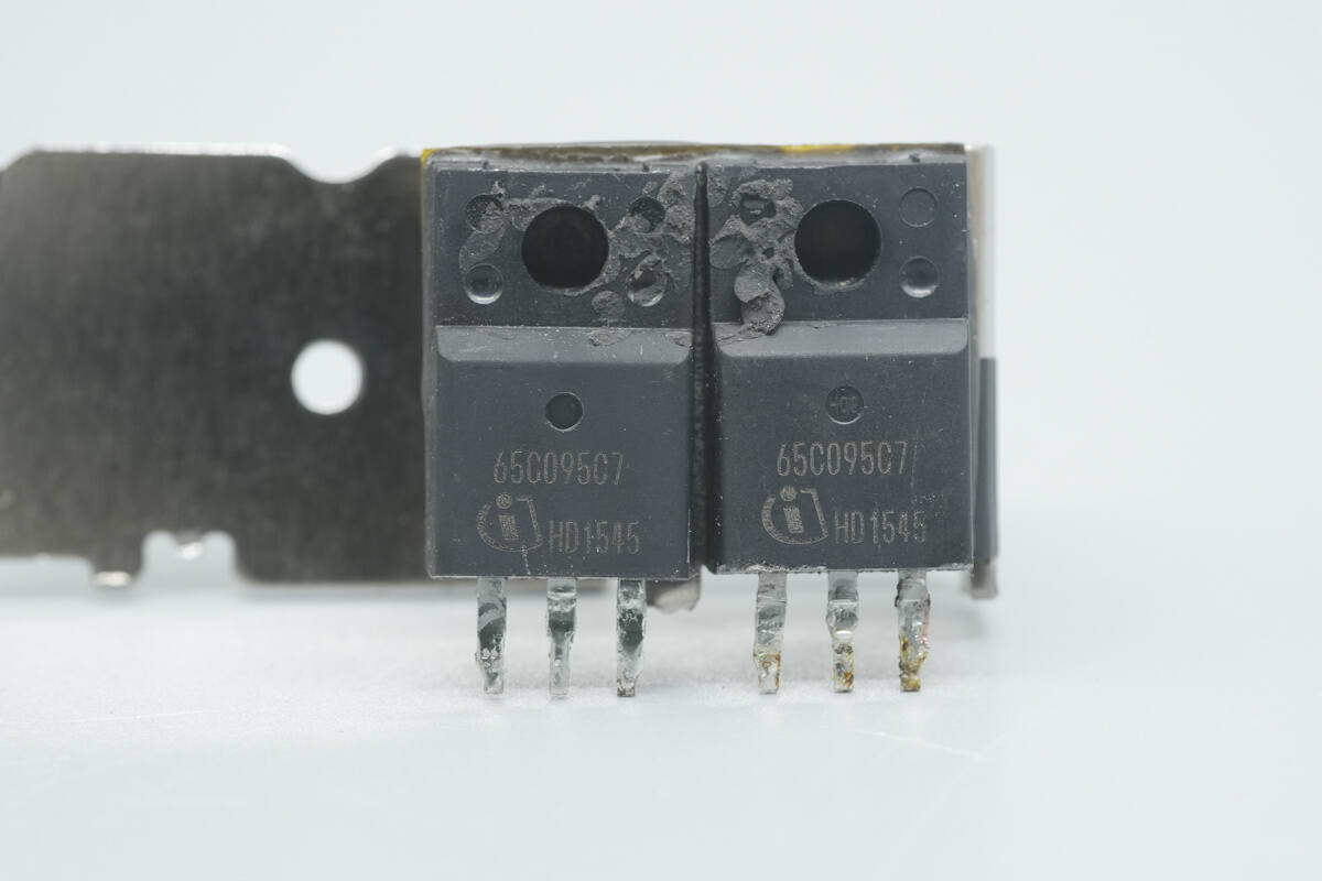
The two active rectification MOSFETs are from Infineon, custom-designed for Apple, marked 65C095C7, in a TO-220FP package, used to improve rectification efficiency.
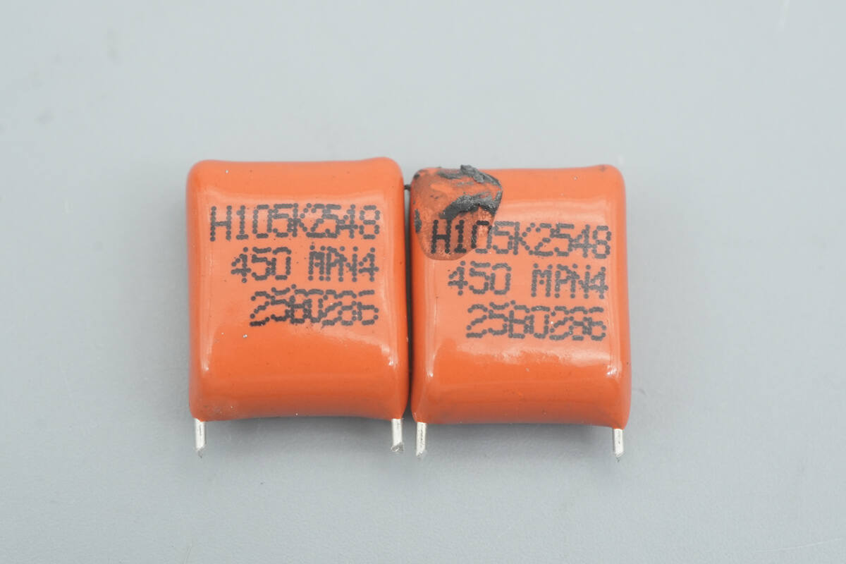
The two film capacitors are rated at 1 μF, 450 V.
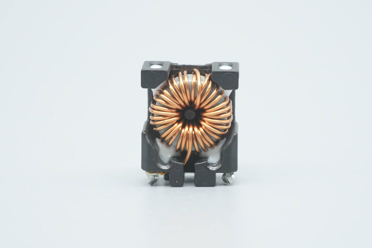
The toroidal filter inductor is reinforced with adhesive.
On the other end, there is a PFC boost inductor and a buck inductor.
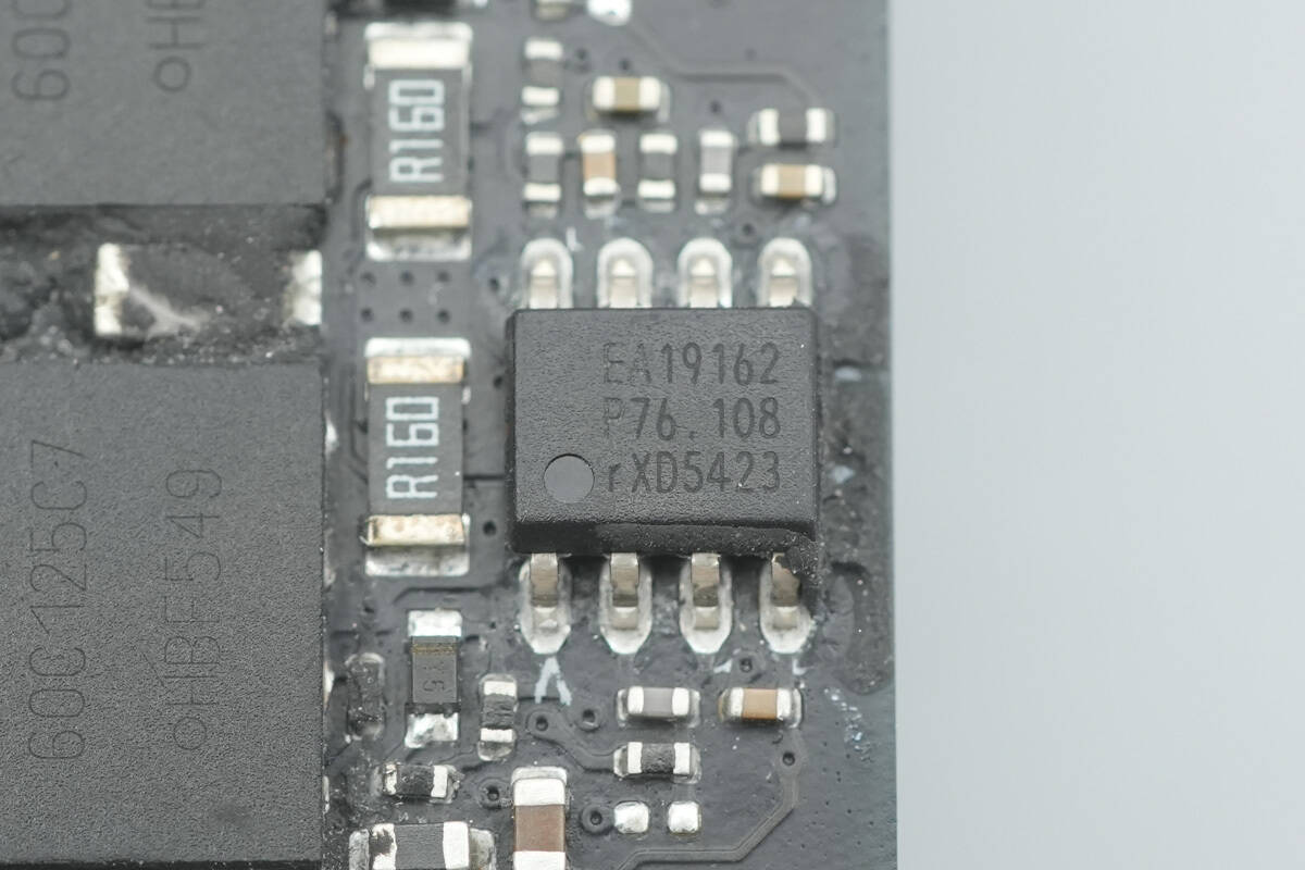
The PFC controller is from NXP, model TEA19162T, featuring integrated X-capacitor discharge functionality and operating in quasi-resonant or DCM. It supports an input voltage range of 70–276 V, includes soft-start and soft-stop functions, and provides precise boost voltage regulation.
The TEA19162T employs valley switching or zero-voltage switching to minimize switching losses, supports frequency limiting to further reduce losses, and burst mode operation to lower power consumption. It comes in an SO8 package.
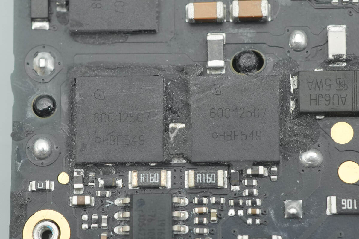
The PFC MOSFETs are from Infineon, marked 60C125C7, and come in a VSON-4 package.
Close-up of the PFC boost inductor.
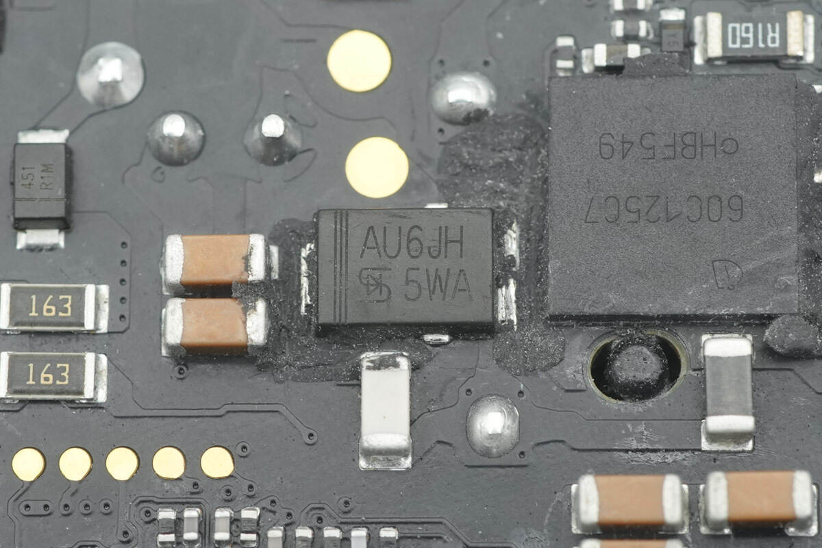
The PFC rectifier is from TSC, model TUAU6JH, a fast-recovery diode rated at 600 V, 6 A, in a TO-277A package.
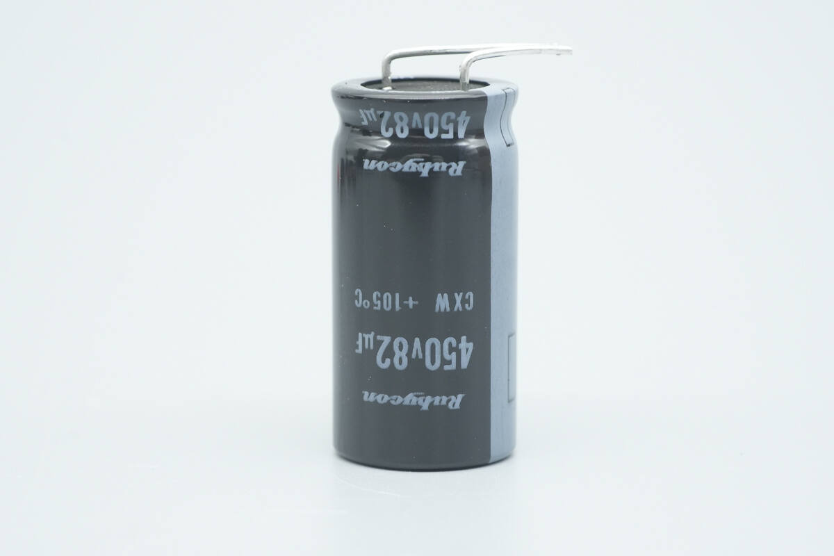
The high-voltage filter electrolytic capacitor is from Rubycon, rated at 450 V, 82 μF.
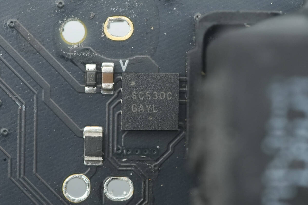
The driver for the Infineon and STMicro MOSFETs is a custom model from Onsemi, marked SC530C.
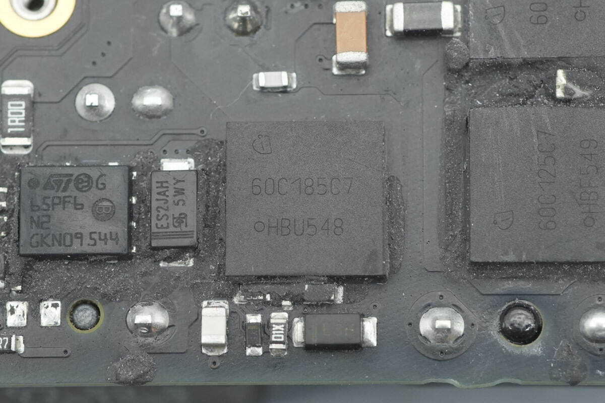
A custom Infineon MOSFET, marked 60C185C7, is an Apple-specific model in a VSON-4 package.
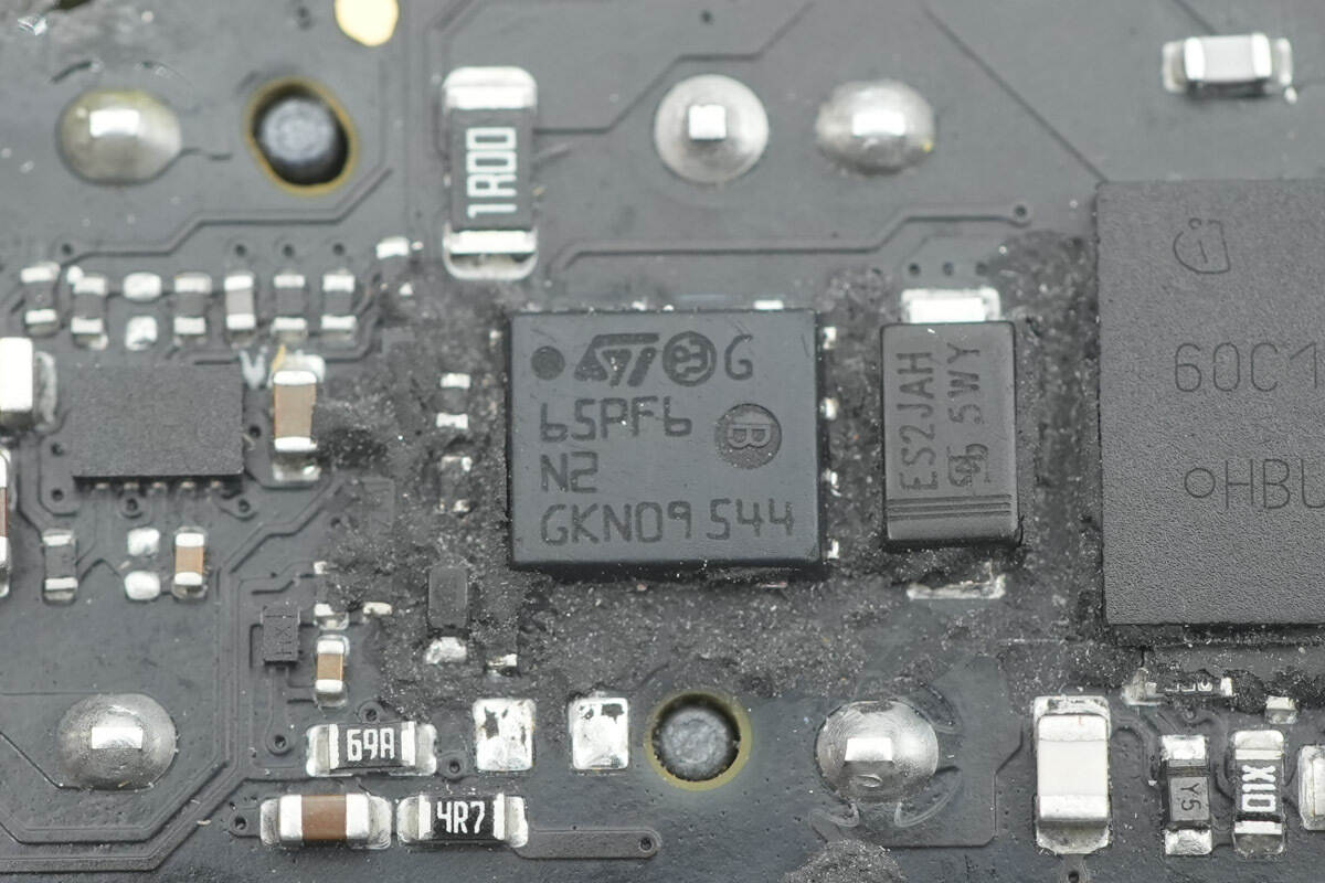
The other MOSFET is from STMicro, marked 65PF6N2, in a PowerFLAT 5×6 HV package.
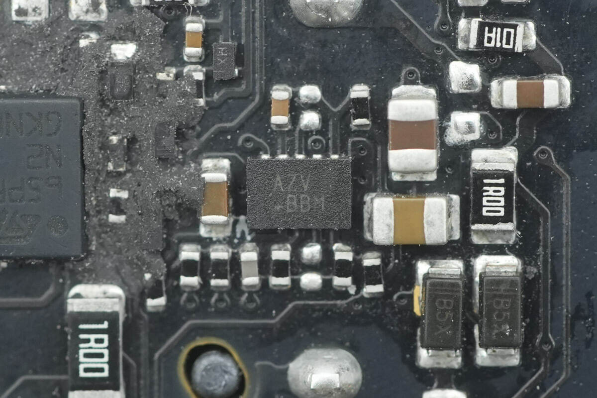
A chip marked with AZV.
A current transformer used to monitor the buck-stage input current.
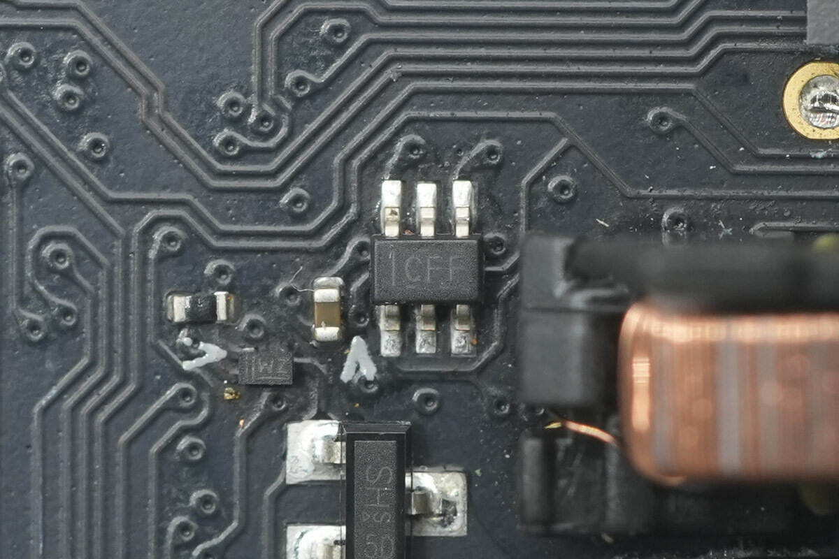
A dual-channel inverter with Schmitt-trigger inputs, operating at 1.65–5.5 V, from TI, marked CFF, model SN74LVC2G14, in an SC70 package.
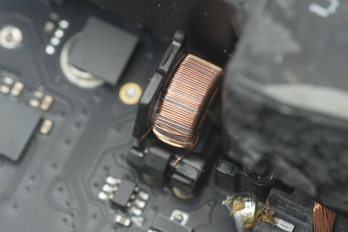
Close-up of the buck inductor.
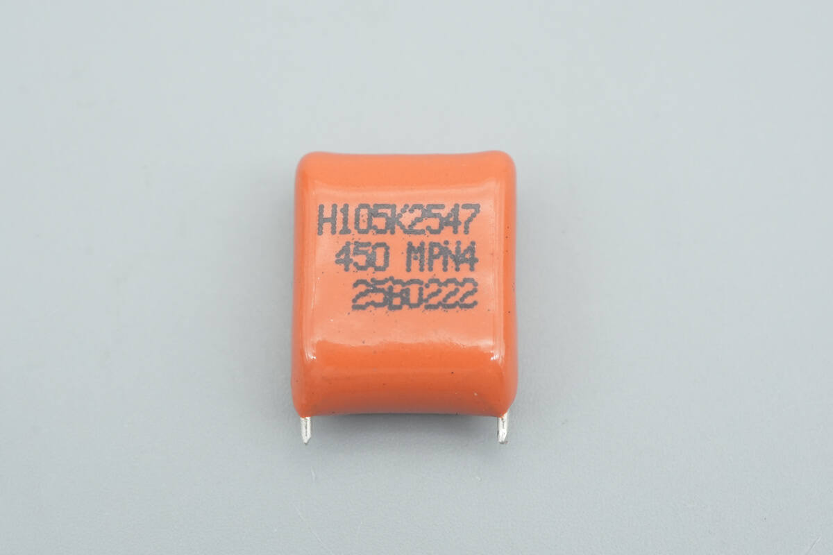
The third film capacitor is rated at 1 μF, 450 V.
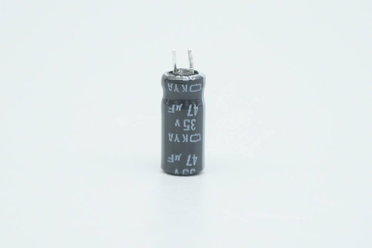
The capacitor supplying power to the master control chip is also from Rubycon, rated at 35 V, 47 μF.
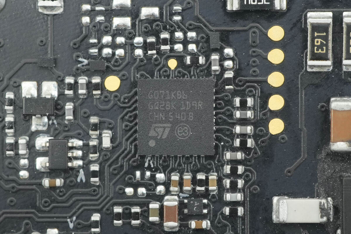
The STMicro STM32G071KB MCU, based on the M0 core, features 128 KB Flash, 36 KB RAM, and a 64 MHz main frequency. It comes in a UFQFPN32 package and is used for primary-side power drive control.
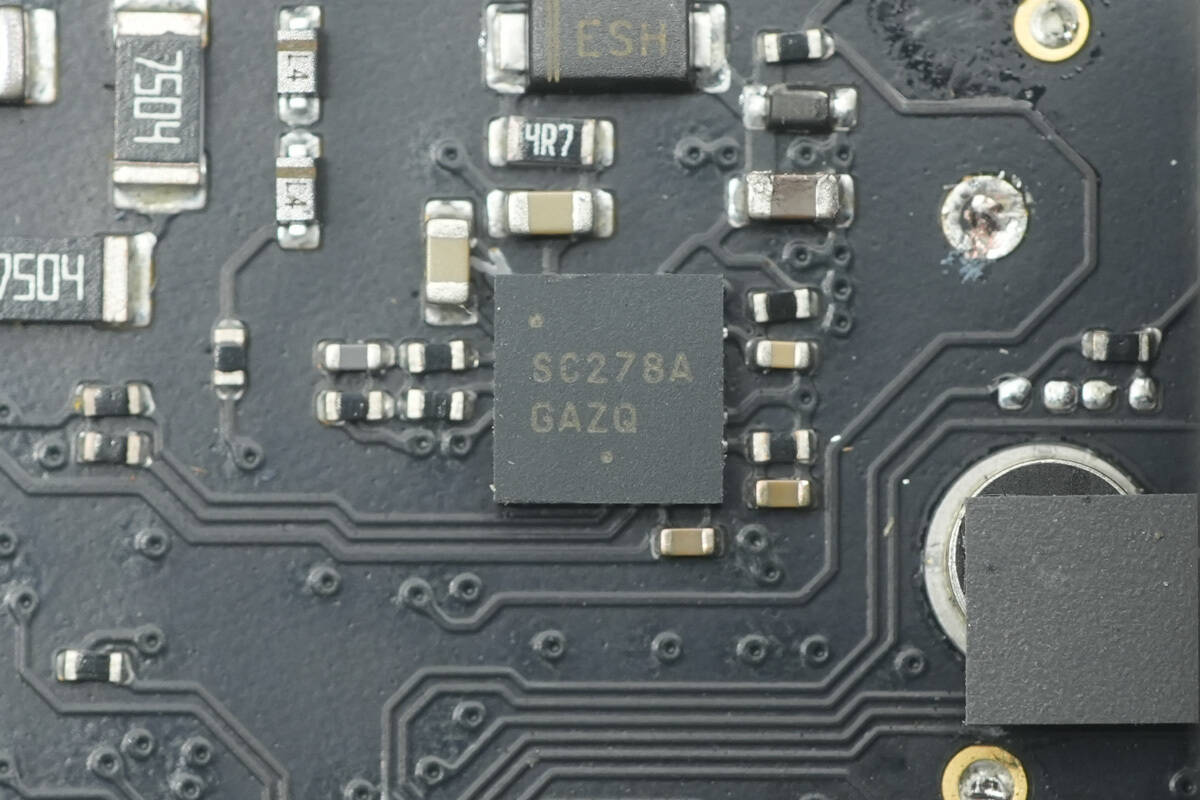
The driver for the two LLC MOSFETs is a custom model from Onsemi, marked SC278A, in a DFN-10 package.
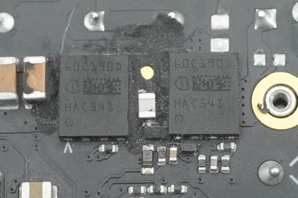
The two LLC MOSFETs are from Infineon, marked 60C190D, an Apple-customized model, in a TSON-8-6 package.
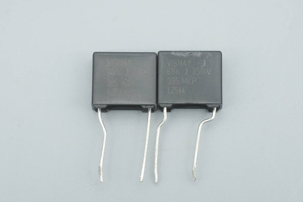
The two resonant capacitors are from VISHAY.
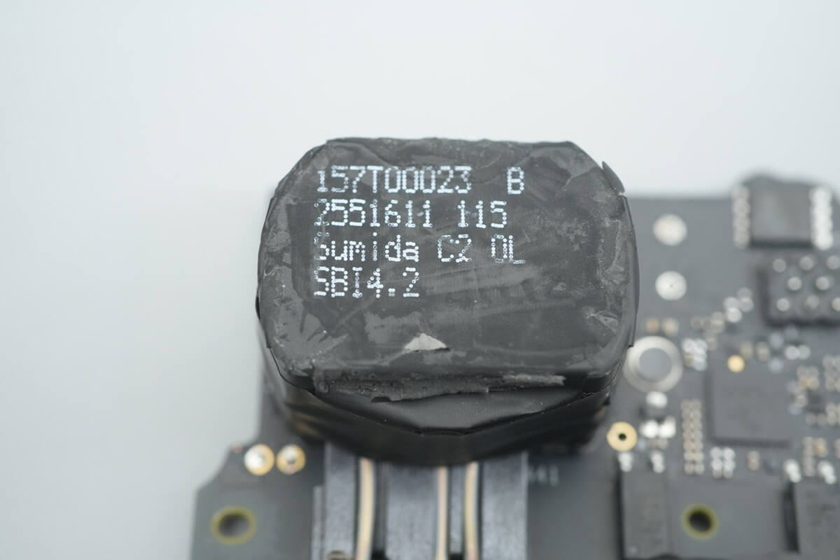
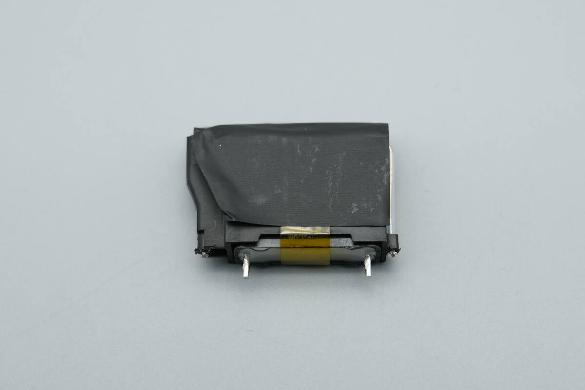
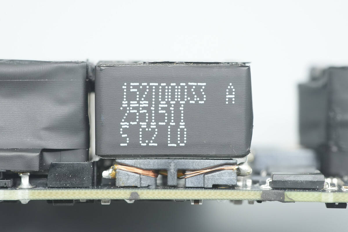
The transformer is supplied by Sumida.
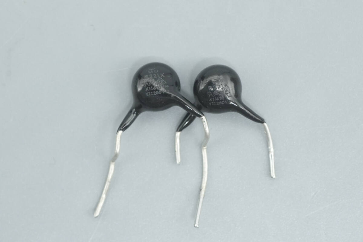
Two black Y capacitors are used for interference suppression.
Two optocouplers are used for output voltage feedback and circuit protection.
Close-up of the third Y capacitor.
Close-up of the buck converter supplying power to the synchronous rectifier controllers.
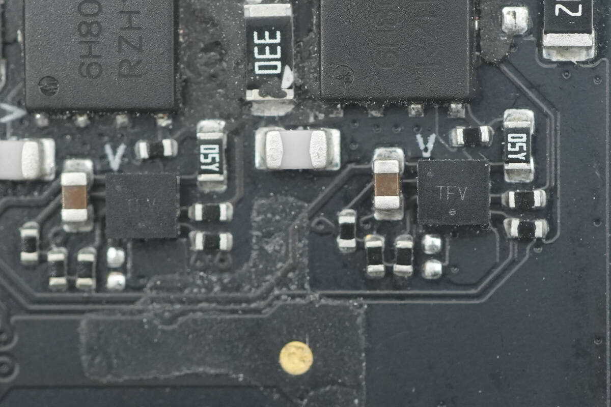
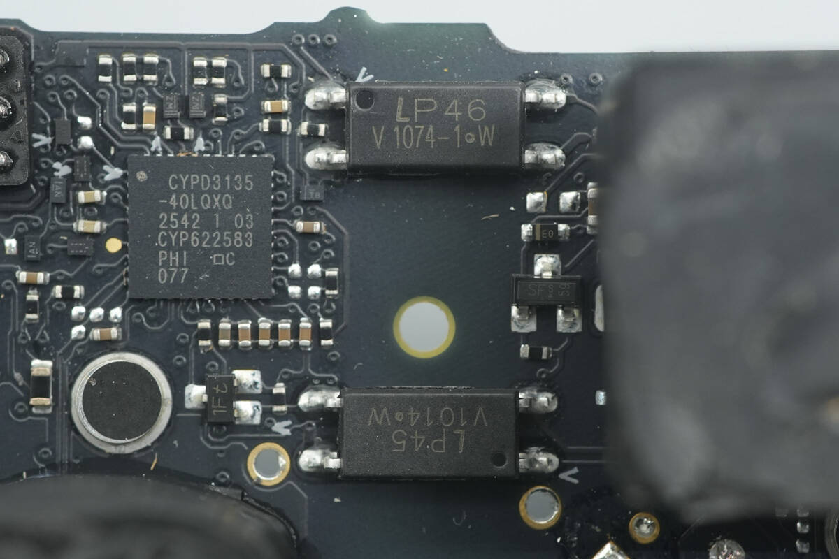
The two custom synchronous rectifier controllers are from Onsemi, marked TFV, in WDFN8 packages.
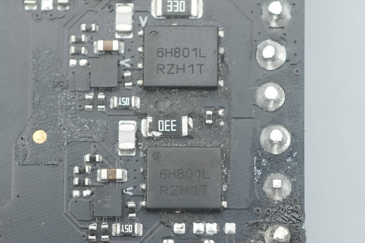
The synchronous rectifiers are from Onsemi, model NTMFS6H801NL, N-channel MOSFETs rated at 80 V with an on-resistance of 2.7 mΩ, in DFN5 packages.
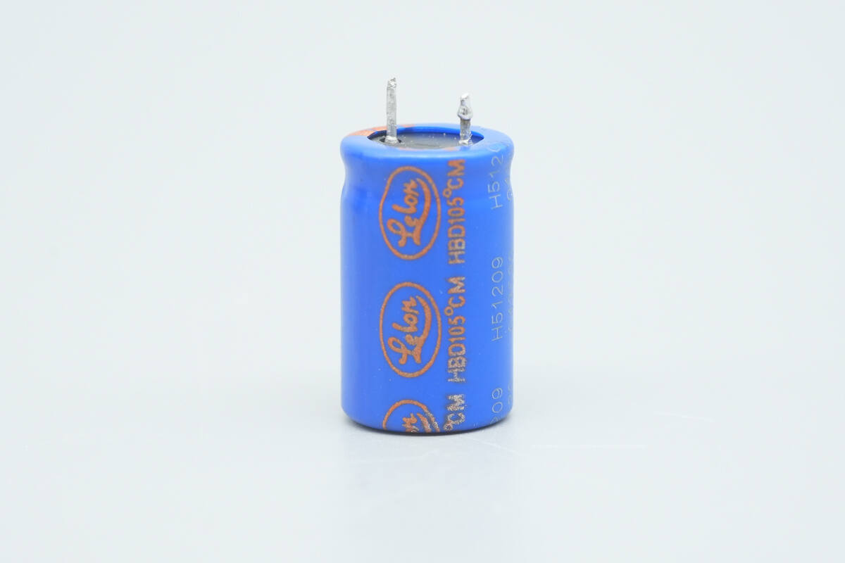
The output filter capacitor is from Lelon.
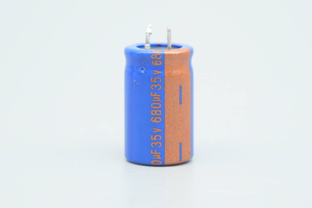
It is rated at 35 V, 680 μF.
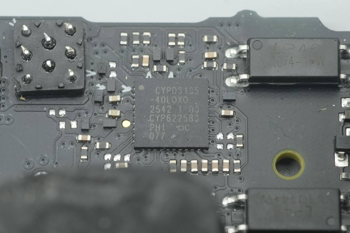
The protocol chip is an Infineon CYPD3135, the industry's first USB PD 3.1 fast-charging protocol chip, custom-designed by Infineon for Apple.
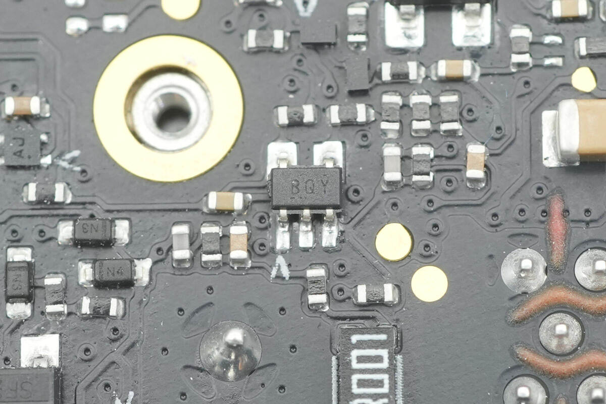
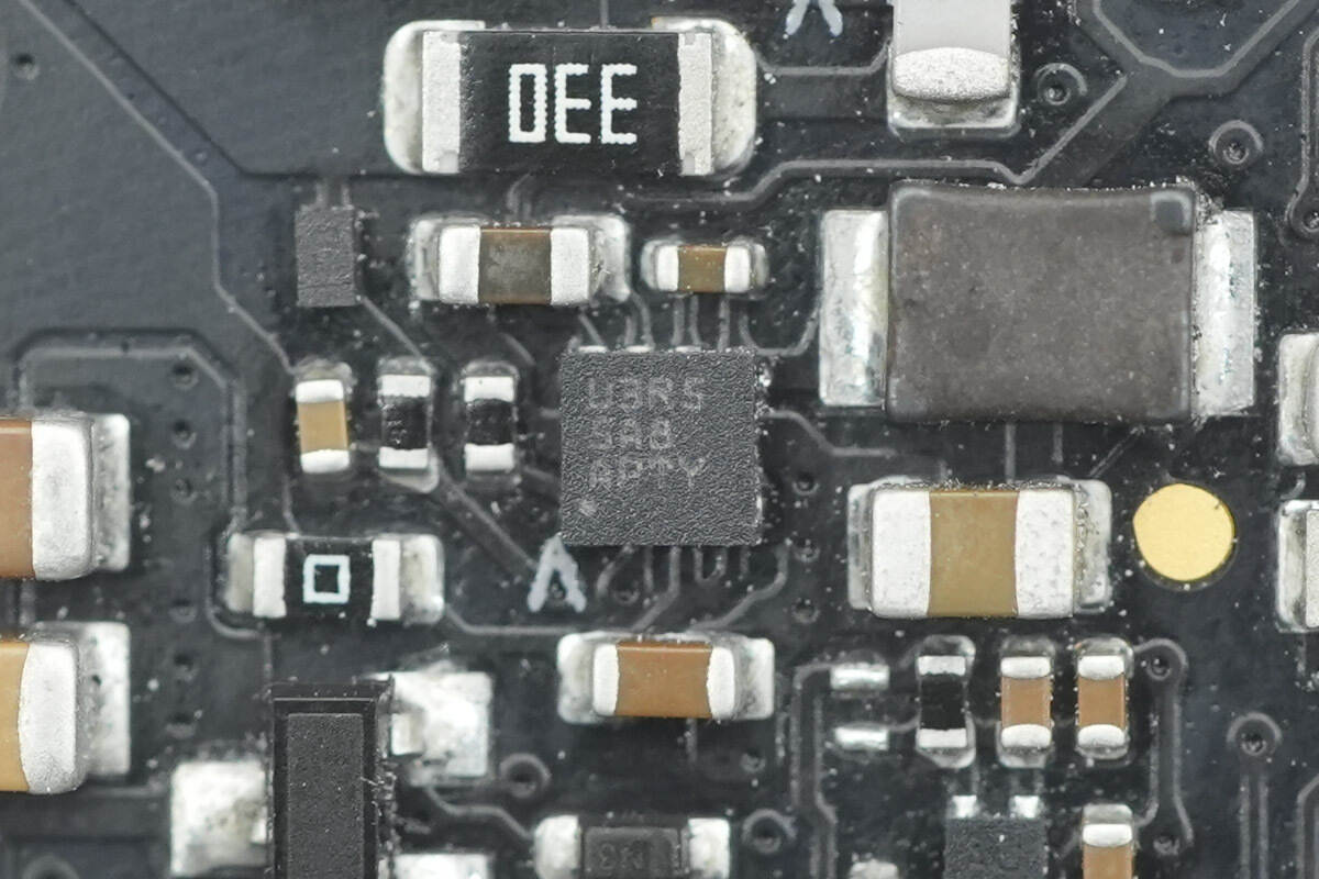
An amplifier used for output current sensing.
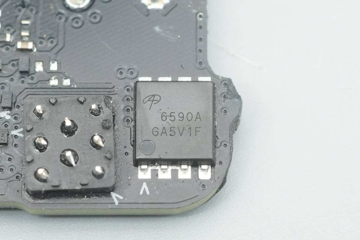
The output VBUS switch is an N-channel MOSFET from AOS, model AON6590A, rated at 40 V with an on-resistance of 0.99 mΩ, in a DFN 5×6 mm package.
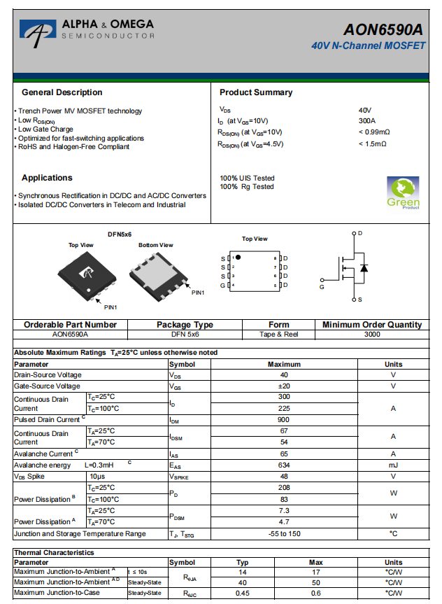
Here is the information about AOS AON6590A.
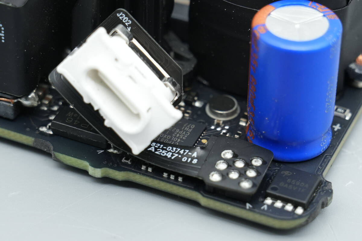
The USB-C socket is connected to the PCBA module via a flexible printed circuit.
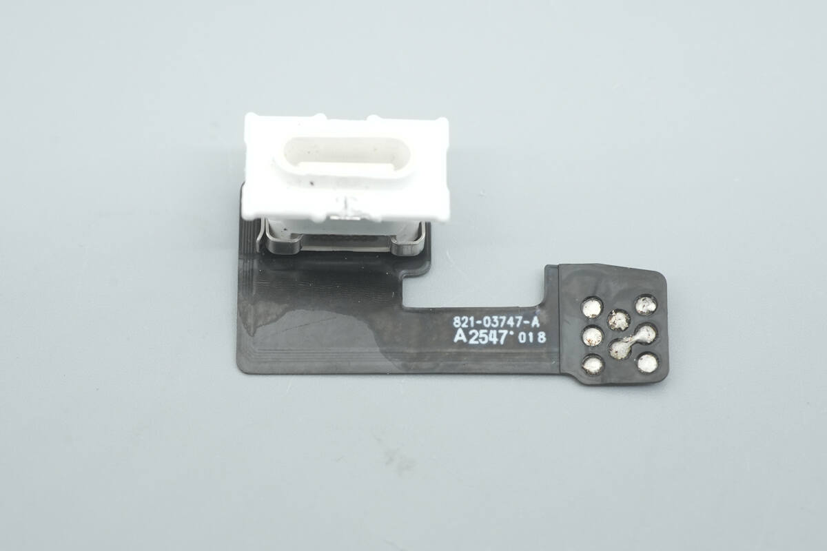
Close-up of the USB-C socket.
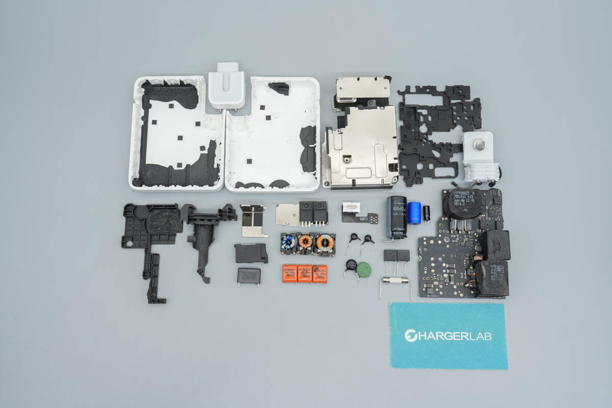
Well, those are all components of the Apple 140W USB-C Power Adapter.
Summary of ChargerLAB
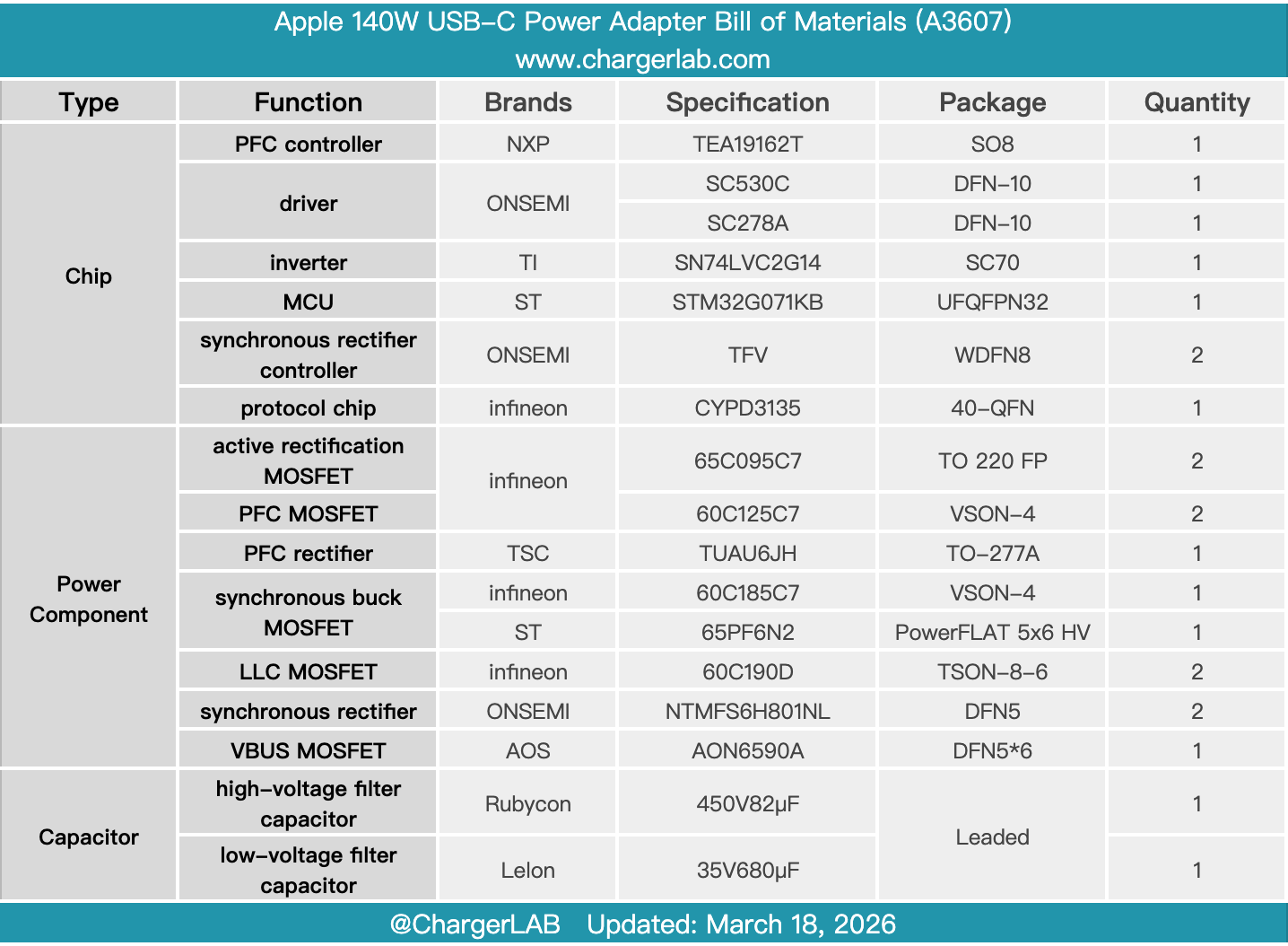
Here is the component list of the Apple 140W USB-C Power Adapter for your convenience.
The A3607 continues Apple’s consistent design language, with appearance and dimensions closely matching the previous generation A2452. However, there are some subtle differences: the removable plug module slot now includes an additional metal clip for auxiliary fixation. As Apple’s flagship power adapter for the new generation of devices, it is also highly compatible with earlier models, delivering up to 140 W PD 3.1 fast charging.
After taking it apart, we found that it uses a high-efficiency architecture of PFC + LLC + synchronous buck, featuring a compact layout and robust thermal design. The controllers are from NXP, STMicro, Onsemi, and Infineon, while most of the power components are custom Infineon products. The design is more integrated and customized, with potential for further improvements in energy efficiency.
Related Articles:
1. Teardown of HuntKey 65W Dual USB-C GaN Charger (H02)
2. Teardown of Samsung 60W Low Standby GaN Charger (EP-T6010)
3. Teardown of MORNSUN 550W Platinum SiC Server Power Supply (LMS550-P12B)