Introduction
Today, we're going to take apart the AOHi The Youth PD 65W GaN 3-Port Charger. It features the brand’s signature yellow color scheme and offers a standard configuration of two USB-C ports and one USB-A port, along with a 65W power output. It also supports UFCS fast charging, with output power reaching up to 63W. Additionally, it’s compatible with QC, PD, PPS, and Huawei’s 22.5W SCP fast charging protocols, making it highly versatile. Next, let’s take it apart to see its internal components and structure.
Product Appearance
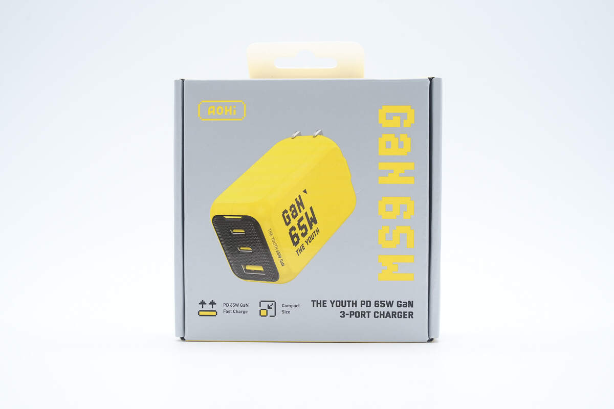
The front of the packaging features the AOHi logo, product name, an image of the charger, and labels such as "GaN 65W."
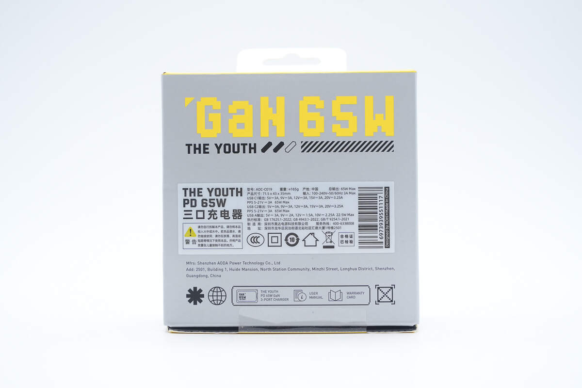
The back of the box displays specifications and other relevant information.
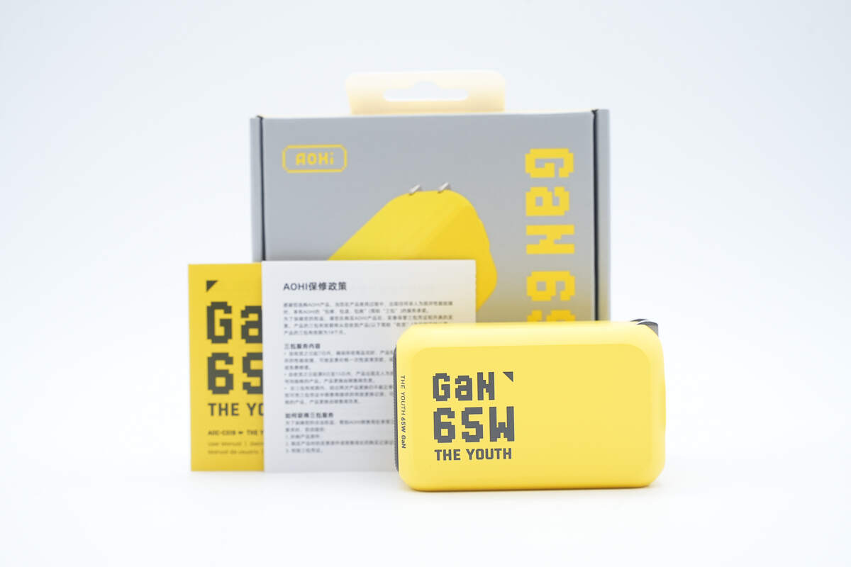
The package includes the charger and some documents.
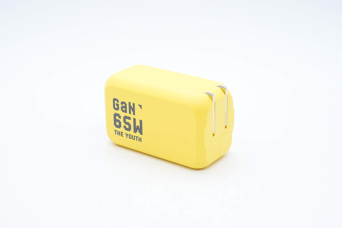
The charger features a black and yellow contrast color design, with smooth transitions between all sides of the casing.
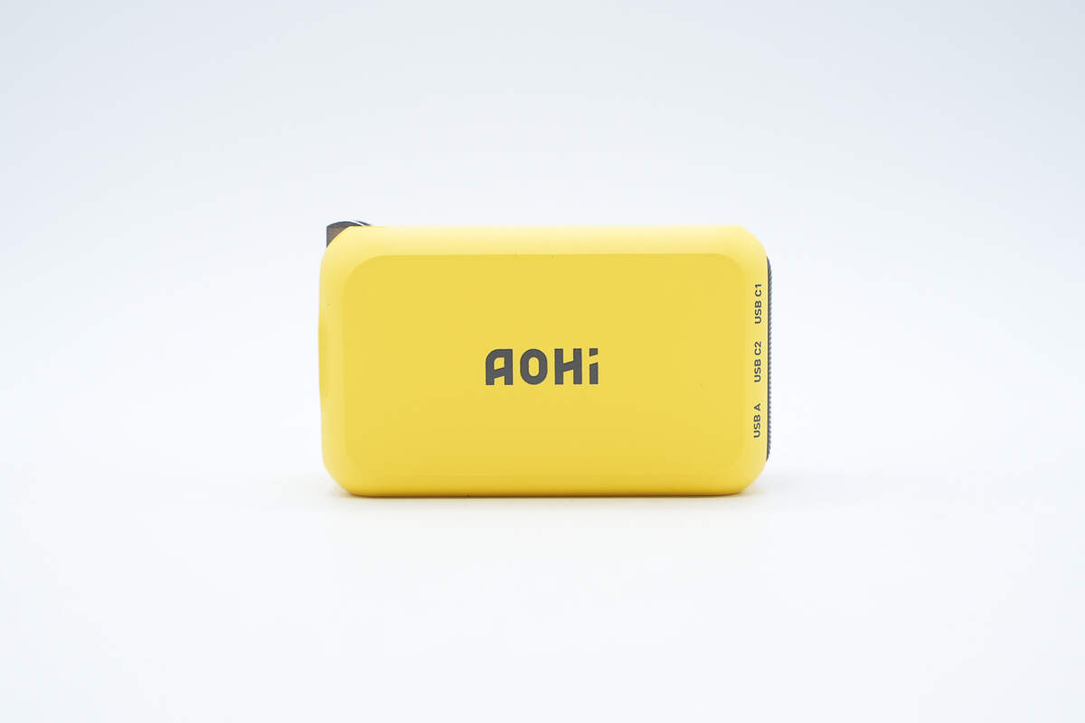
The center of the front side is printed with the AOHi logo.
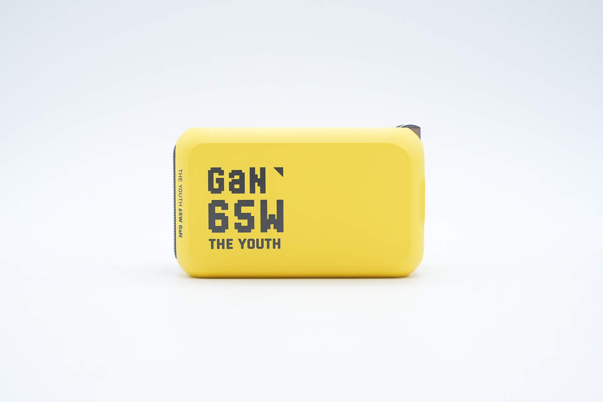
The back is printed with GaN 65W THE YOUTH.
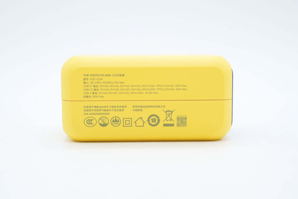
The side panel displays the spec info.
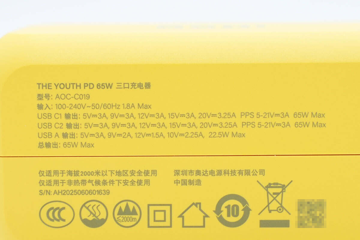
Model: AOC-C019
Input: 100-240V\~ 50/60Hz 1.8A Max
Output:
USB-C1: 5V 3A, 9V 3A, 12V 3A, 15V 3A, 20V 3.25A; PPS 5-21V 3A; 65W Max
USB-C2: 5V 3A, 9V 3A, 12V 3A, 15V 3A, 20V 3.25A; PPS 5-21V 3A; 65W Max
USB-A: 5V 3A, 9V 2A, 12V 1.5A, 10V 2.25A; 22.5W Max
Total Output: 65W Max
Manufacturer: Shenzhen Aoda Power Technology Co., Ltd.
The charger is CCC certified.
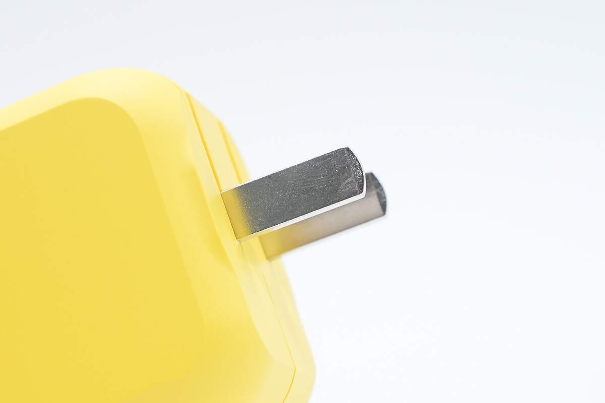
It comes with foldable plugs.
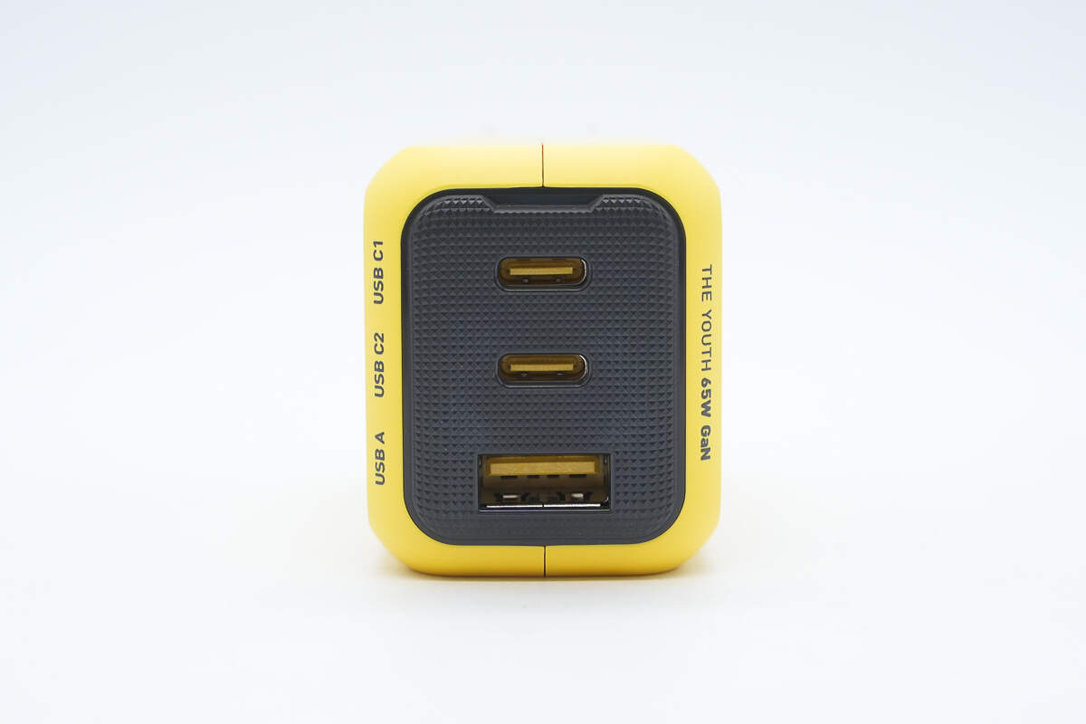
The top panel is equipped with two USB-C ports and one USB-A port.
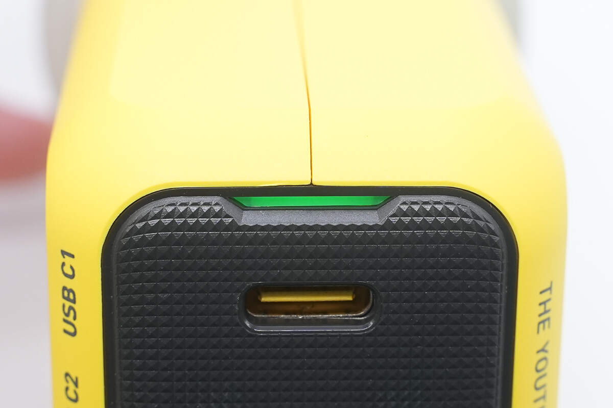
The edge features a soft tri-color breathing indicator light. During charging, it automatically switches between yellow, blue, and green lights to indicate low battery, sufficient charge, and full battery status, respectively.
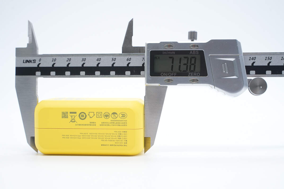
The length of the charger is about 71.38 mm (2.81 inches).
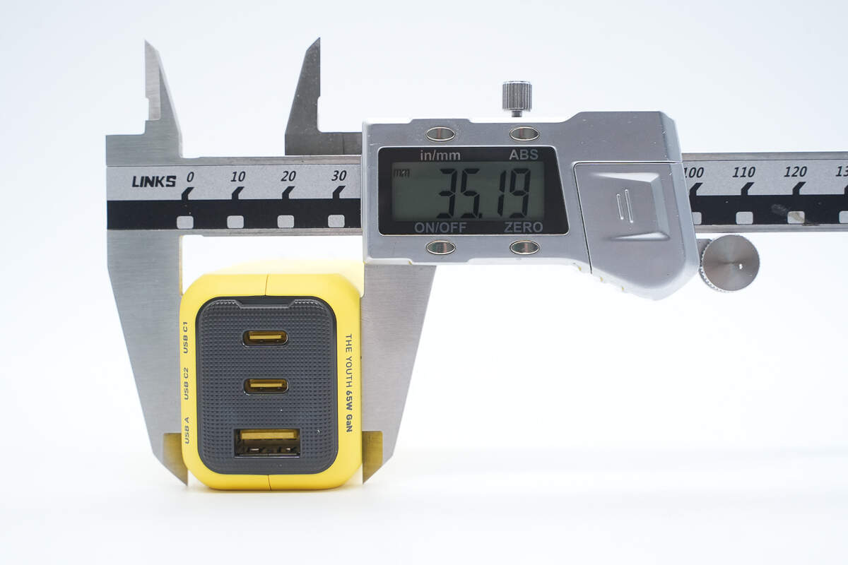
The width is about 35.19 mm (1.39 inches).
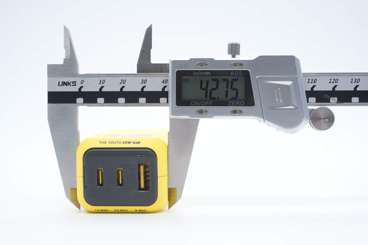
The thickness is about 42.75 mm (1.68 inches).
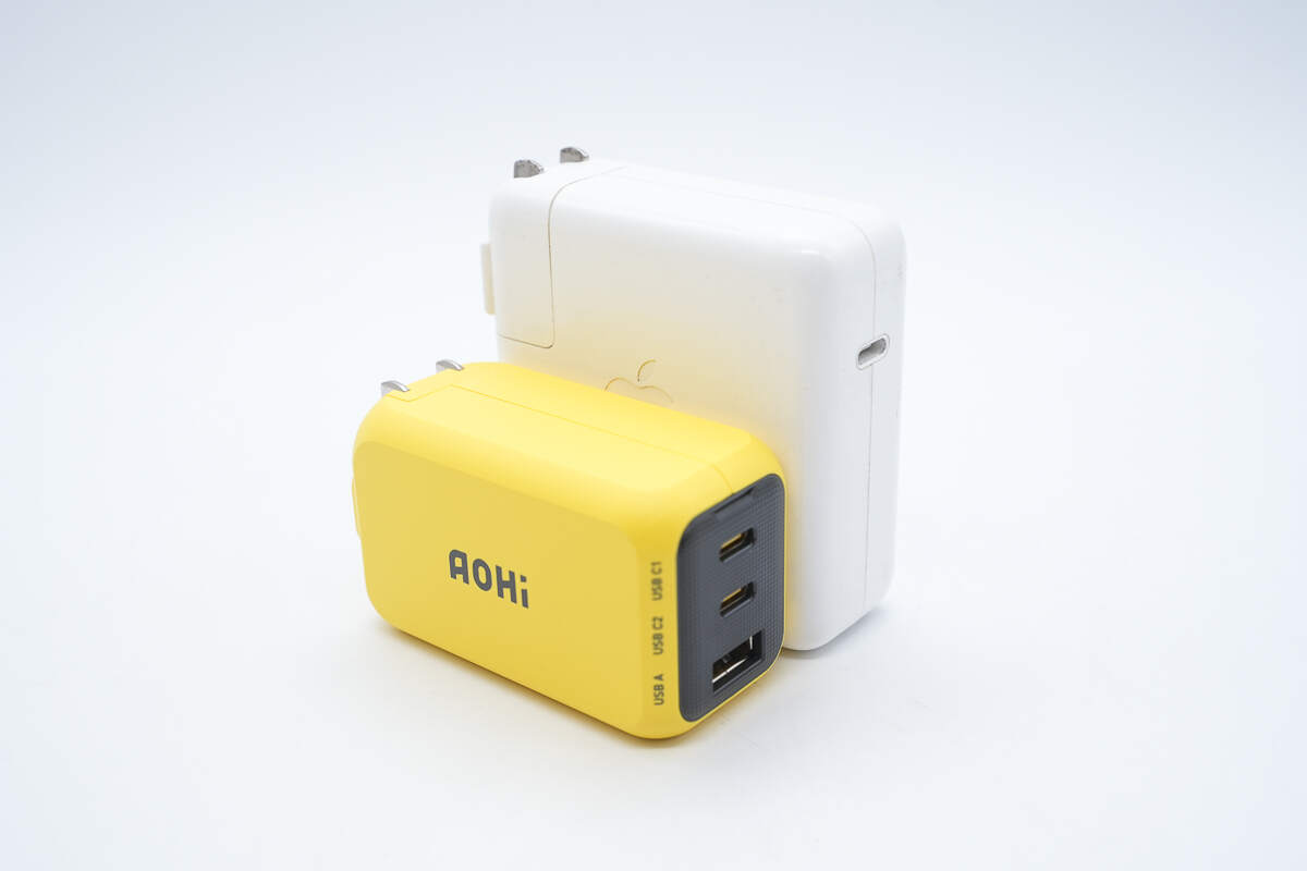
It is significantly smaller than the Apple 67W charger.

That's how big it is in the hand.
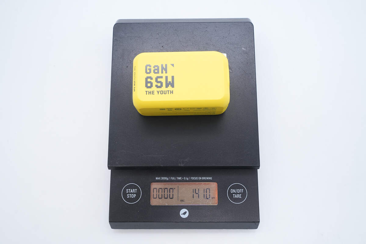
The weight is about 141 g (4.97 oz).
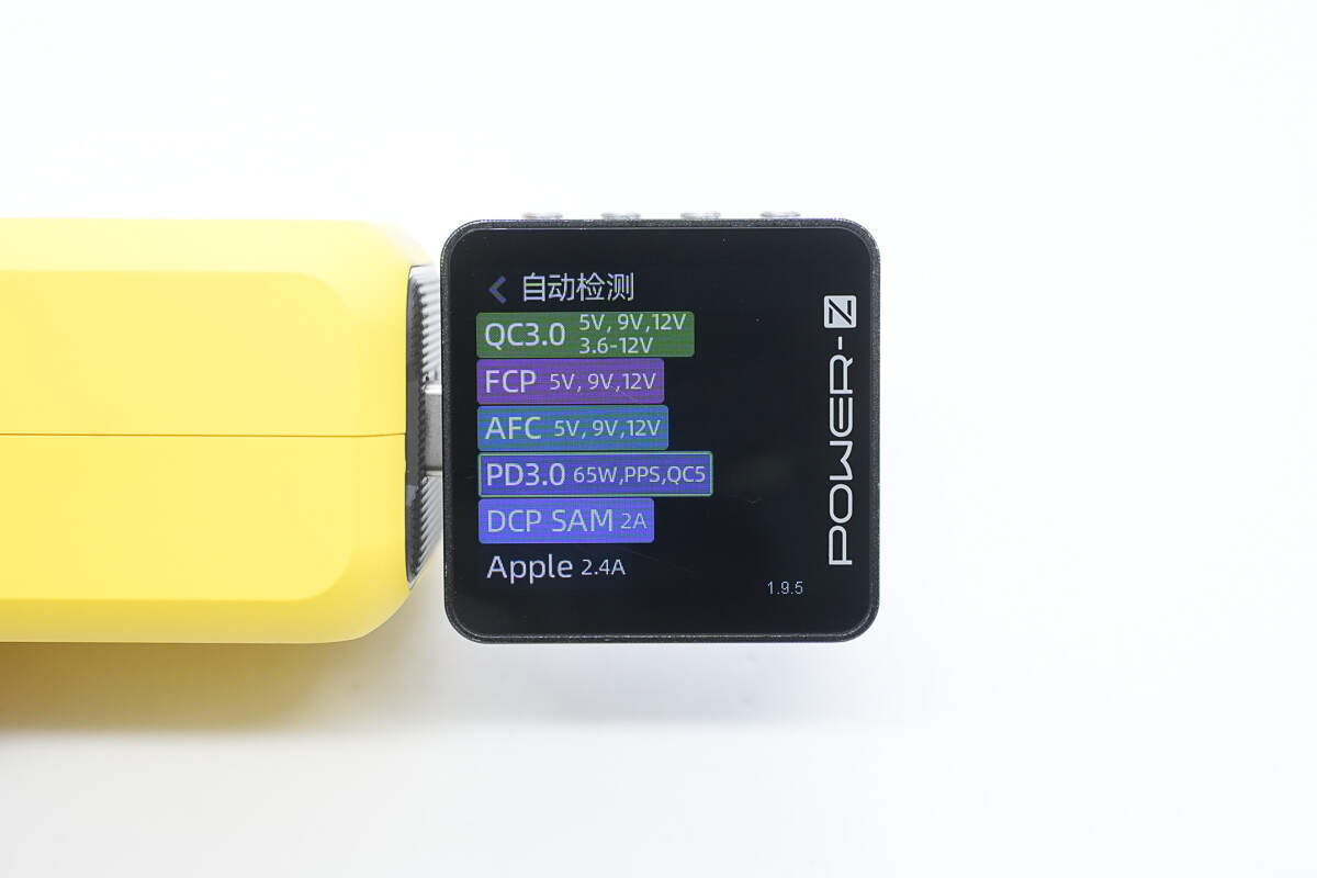
ChargerLAB POWER-Z KM003C shows that the USB-C1 supports QC3.0/5, FCP, AFC, PD3.0, PPS, DCP, SAM 2A, and Apple 2.4A charging protocols.
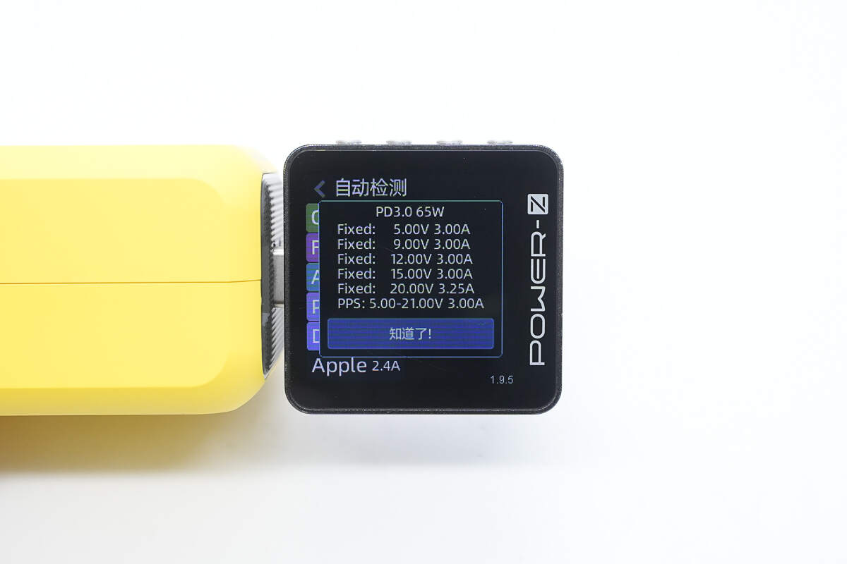
And it has five fixed PDOs of 5V3A, 9V3A, 12V3A, 15V3A, and 20V3.25A. It has one set of PPS, which is 5-21V3A.
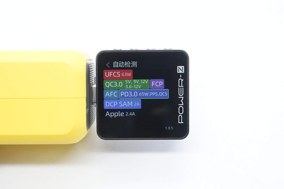
The USB-C2 supports UFCS, QC3.0/5, FCP, AFC, PD3.0, PPS, DCP, SAM 2A, and Apple 2.4A charging protocols.
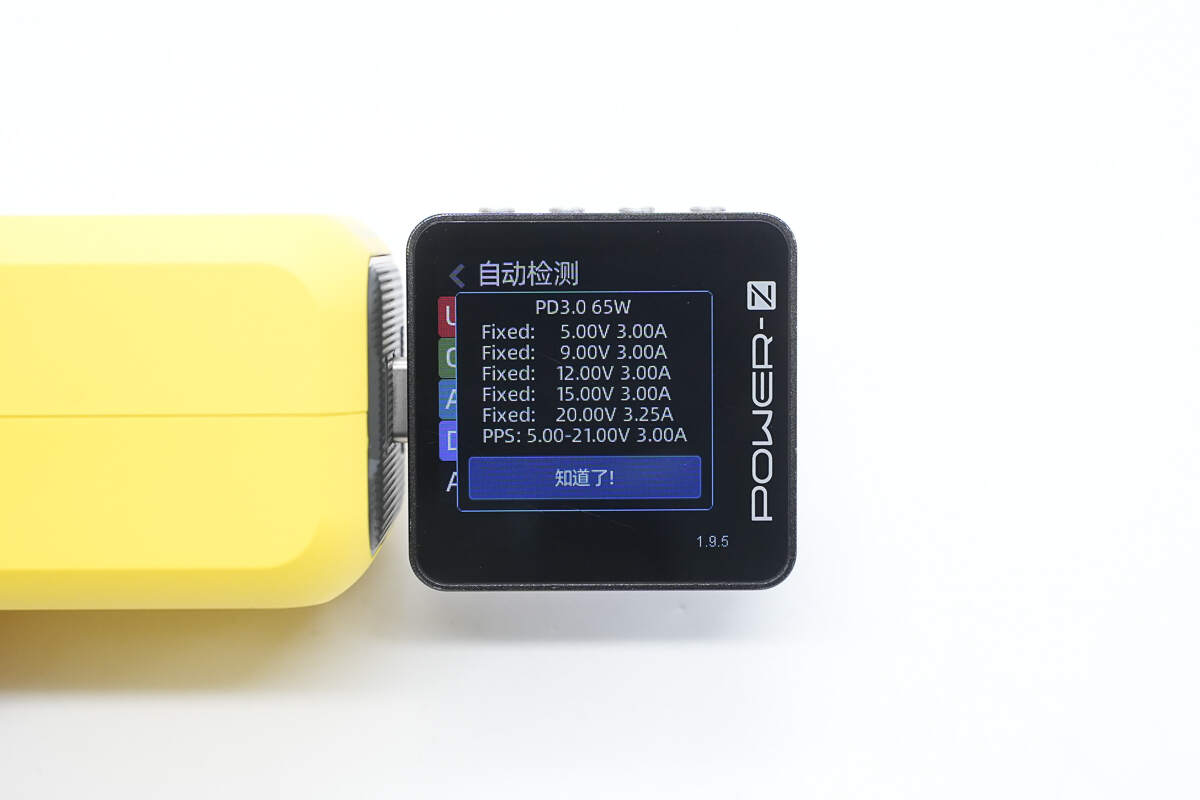
And it has five fixed PDOs of 5V3A, 9V3A, 12V3A, 15V3A, and 20V3.25A. It has one set of PPS, which is 5-21V3A.
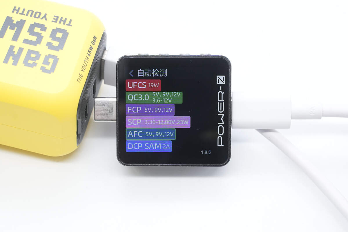
The USB-A supports UFCS, QC3.0, FCP, SCP, AFC, DCP, and SAM 2A charging protocols.
Teardown
Next, let's take it apart to see its internal components and structure.
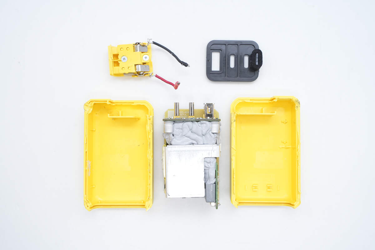
Open the casing and remove the PCBA module.
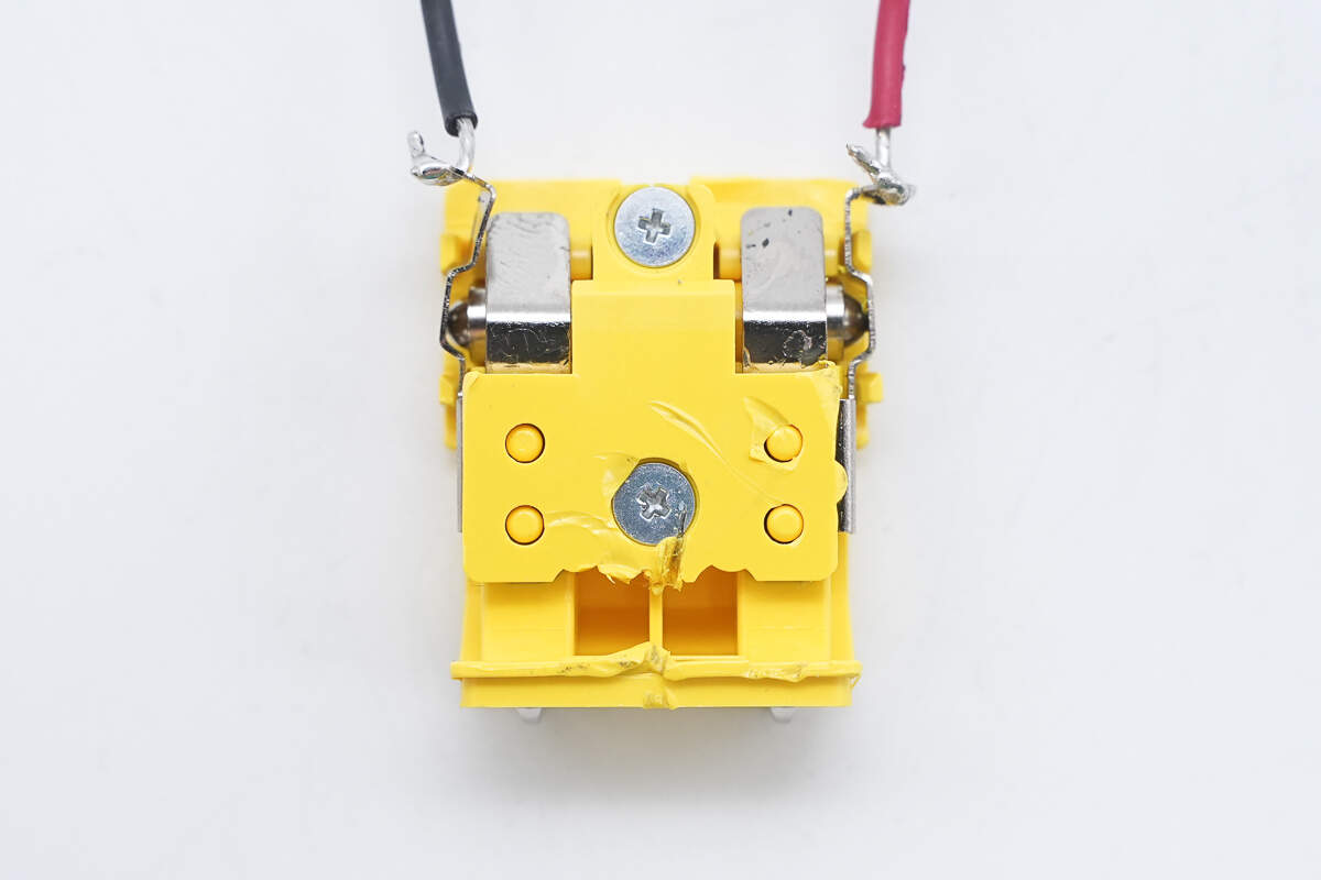
The plug is secured using screws and a plastic plate. Electrical connection is achieved through exposed spring contacts soldered to the wires.
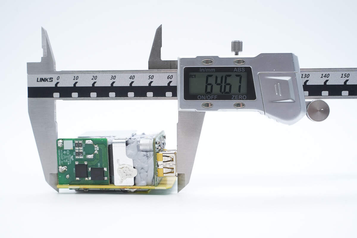
The length of the PCBA module is about 64.67 mm (2.55 inches).
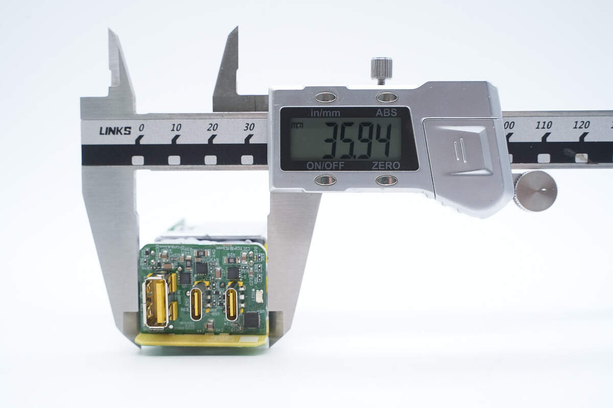
The width is about 35.94 mm (1.41 inches).
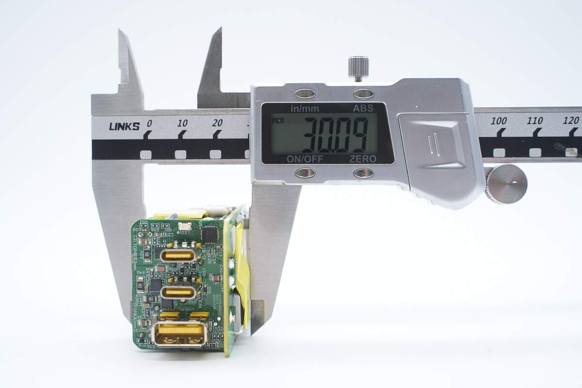
The thickness is about 30.09 mm (1.18 inches).
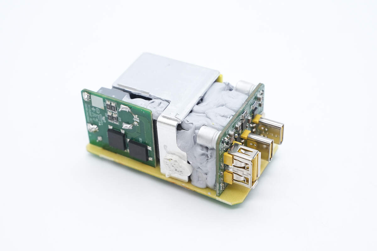
There are small PCBs on the side and the output end of the PCBA module. Potting compound is used between components for insulation and stability. The top and sides are covered with an integrated heatsink for thermal management.
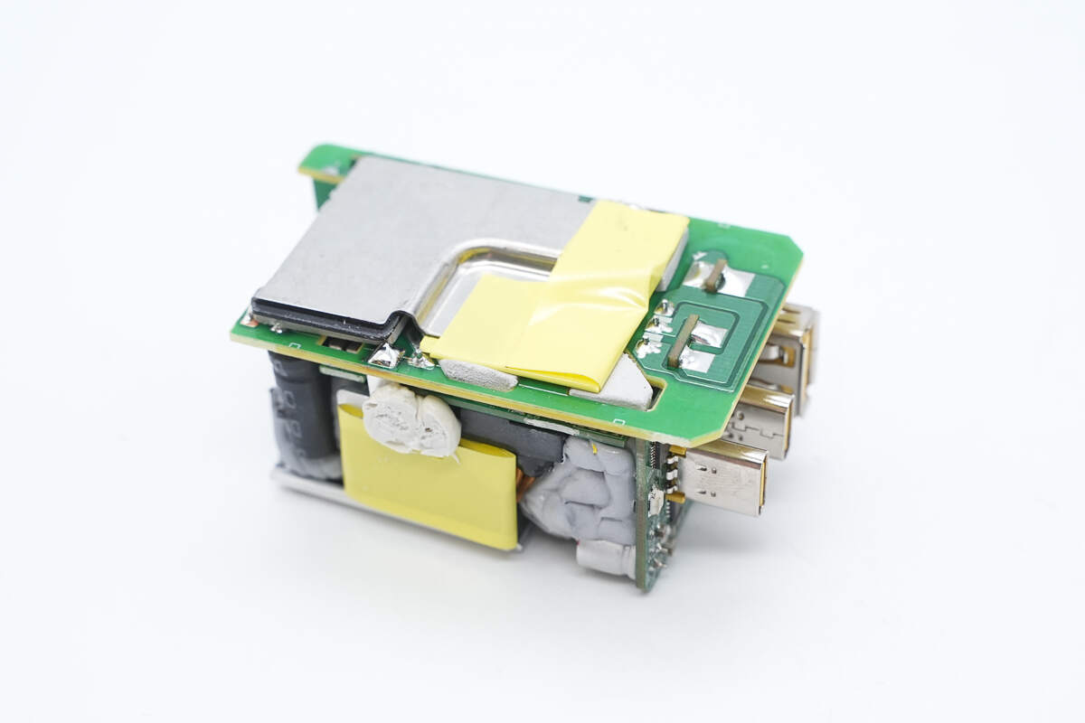
The back side is also covered with a heatsink.
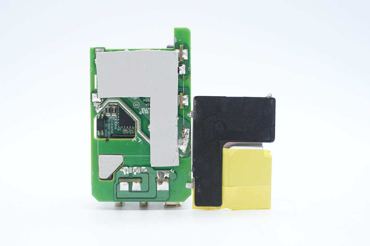
After removing the heatsink, insulation tape and Mylar sheets are found adhered to the inner side. Thermal pads are attached to the PCB to aid heat dissipation.
After cleaning off the potting compound, a third small PCB is revealed underneath the transformer.
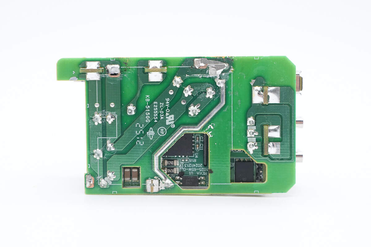
There are no components on the back of the main PCB. The areas corresponding to the master control chip and the synchronous rectifier are hollowed out for better heat dissipation.
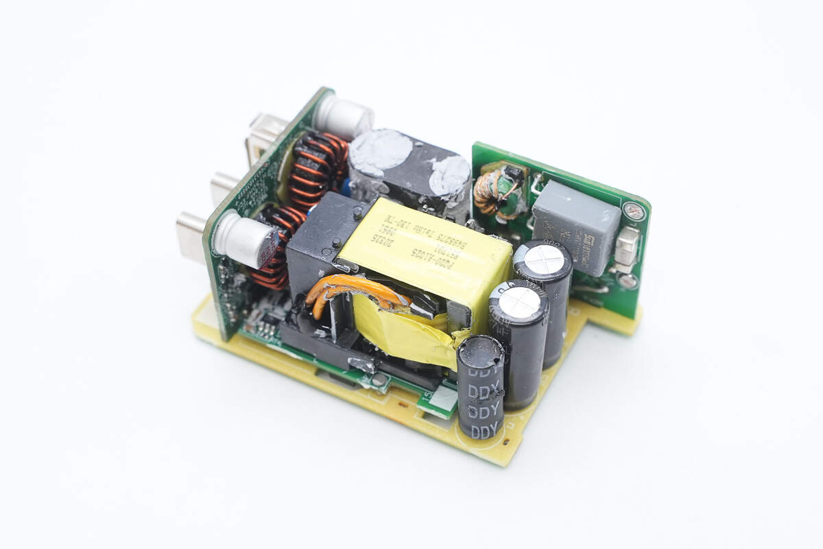
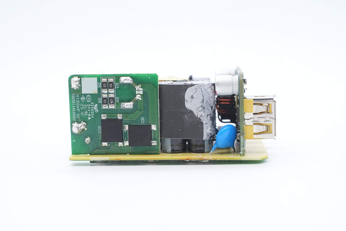
At the input end of the module, there are electrolytic capacitors and an I-shaped inductor. A small PCB is soldered on the right side.
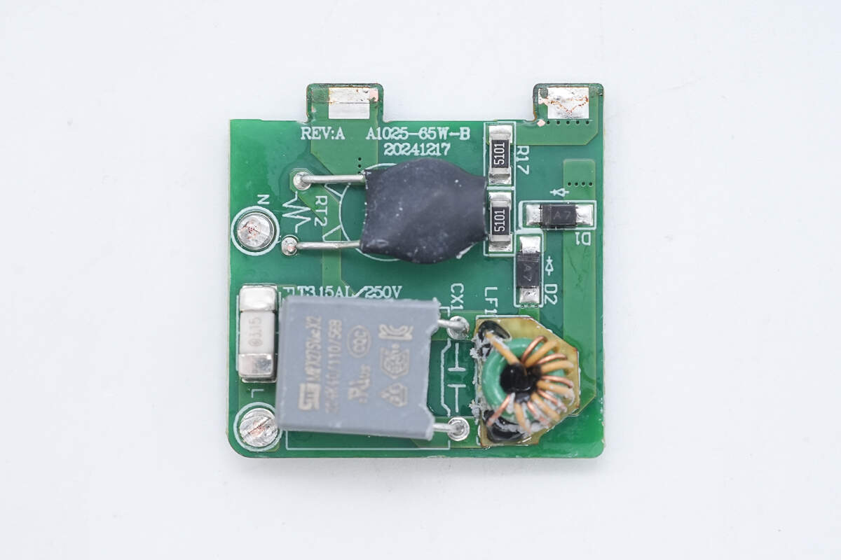
After removing the small PCB, the front side reveals an SMD fuse, an NTC thermistor, a safety X2 capacitor, and a common mode choke.
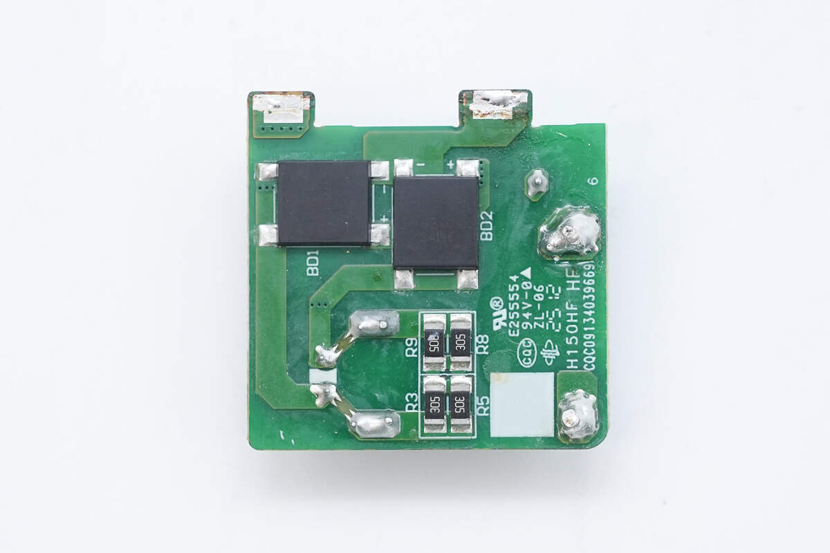
The back side is equipped with two bridge rectifiers.
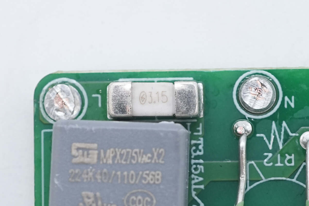
The SMD fuse is from Betterfuse and has a rated current of 3.15A.
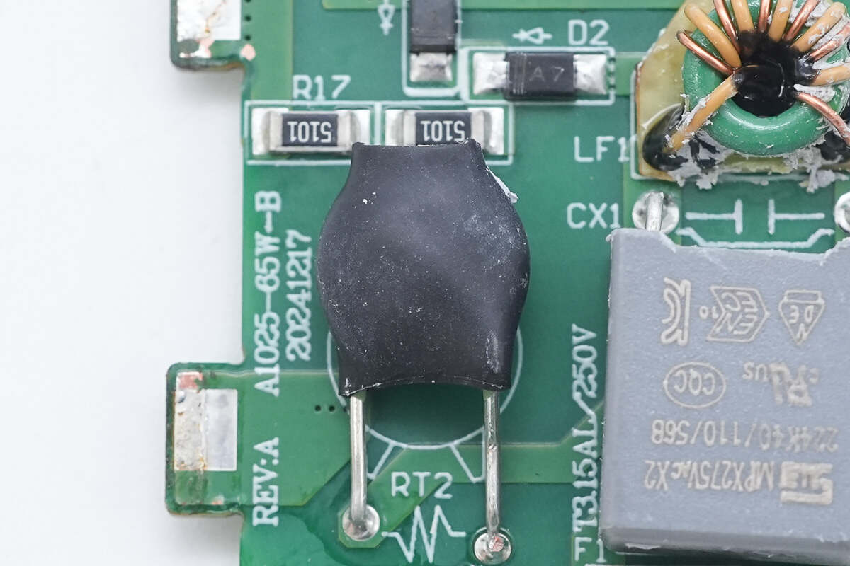
The NTC thermistor is insulated with heat-shrink tubing.
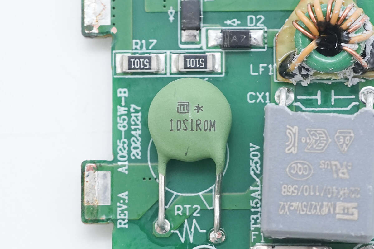
The NTC thermistor is used to suppress inrush current when powering on.
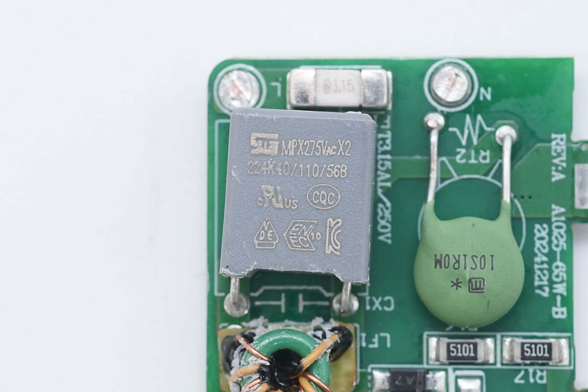
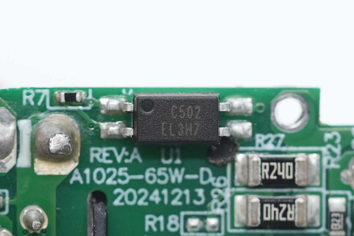
The safety X2 capacitor is from STE and has a capacitance of 0.22μF.
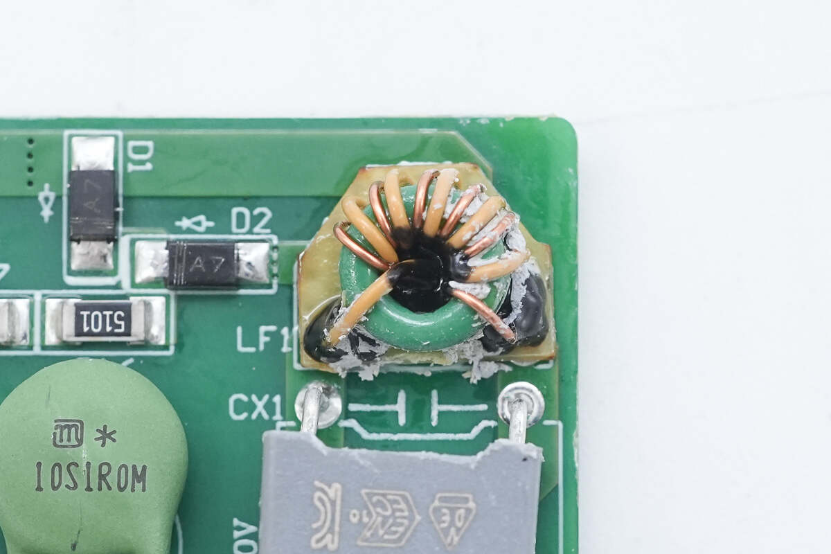
The common mode choke is used to filter out EMI interference, and it is also insulated with Bakelite.
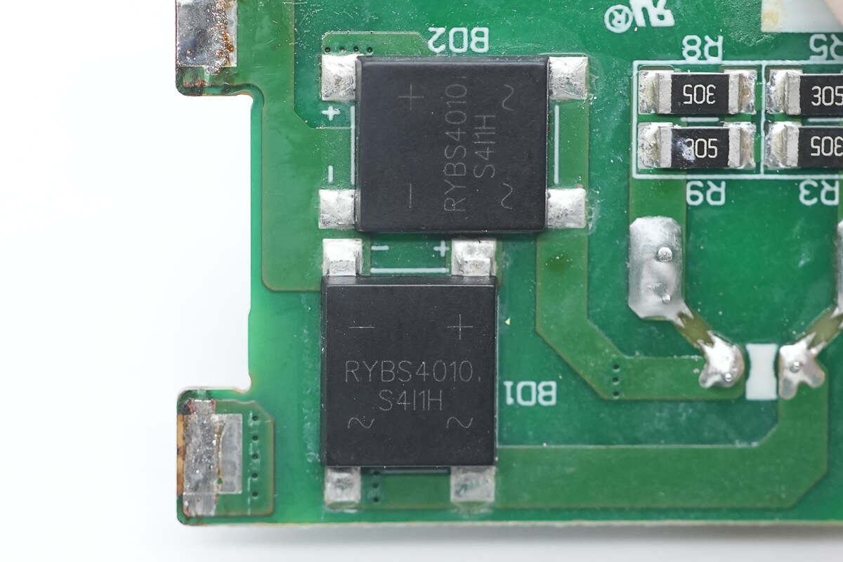
The two bridge rectifiers are model RYBS4010, rated at 4A 1000V, and use TMBF packaging.
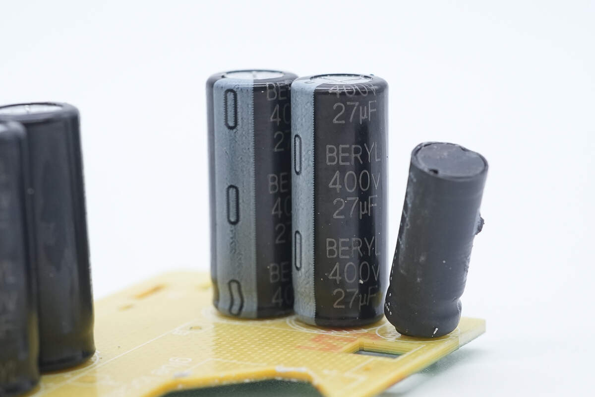
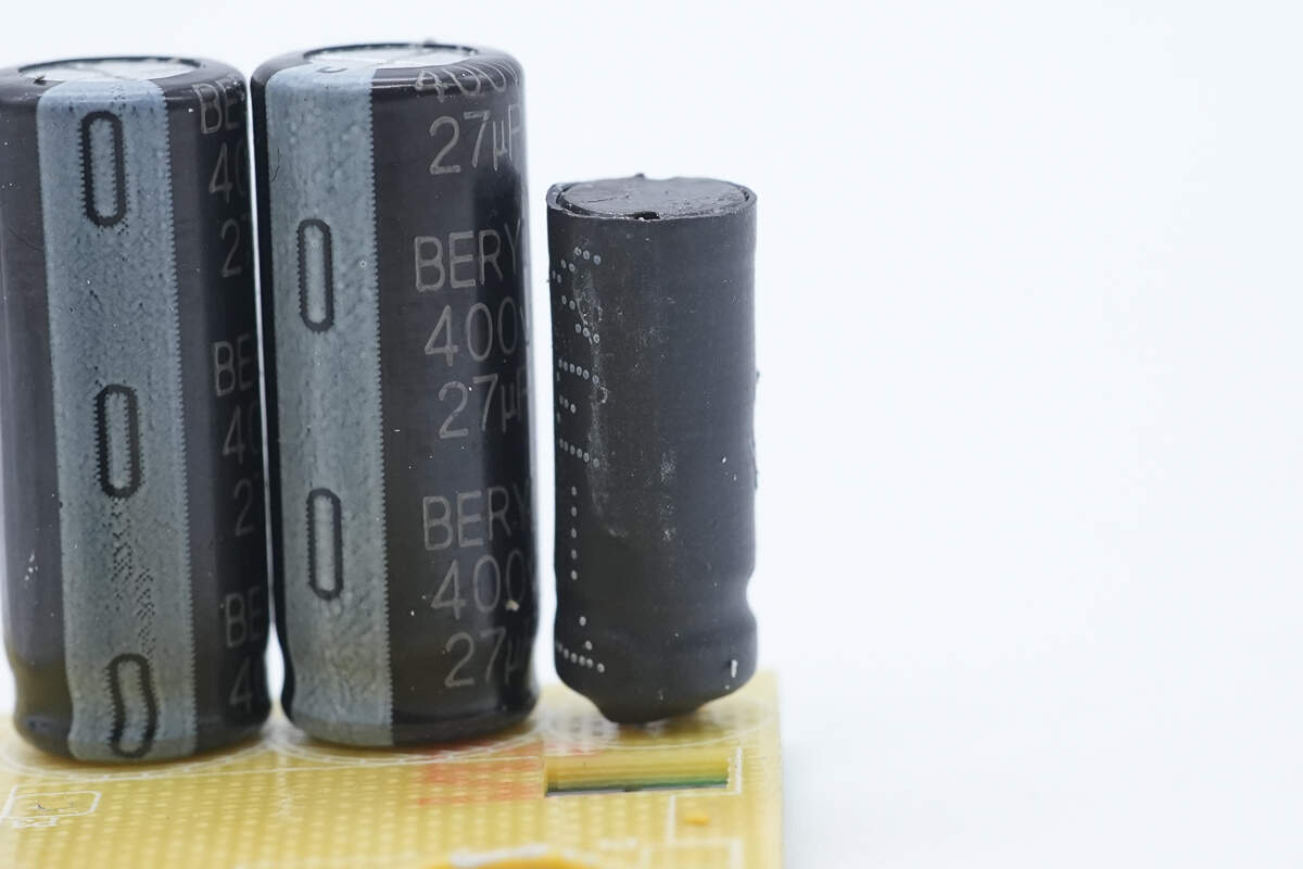
The two electrolytic capacitors are from BERYL, each rated at 400V 27μF.
The nearby I-shaped inductor is insulated with heat-shrink tubing.
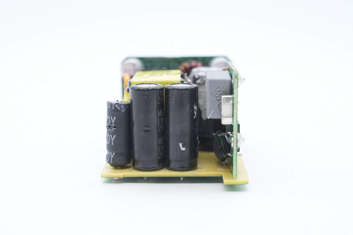
On the side, there are also two electrolytic capacitors, each covered with insulating sleeves.
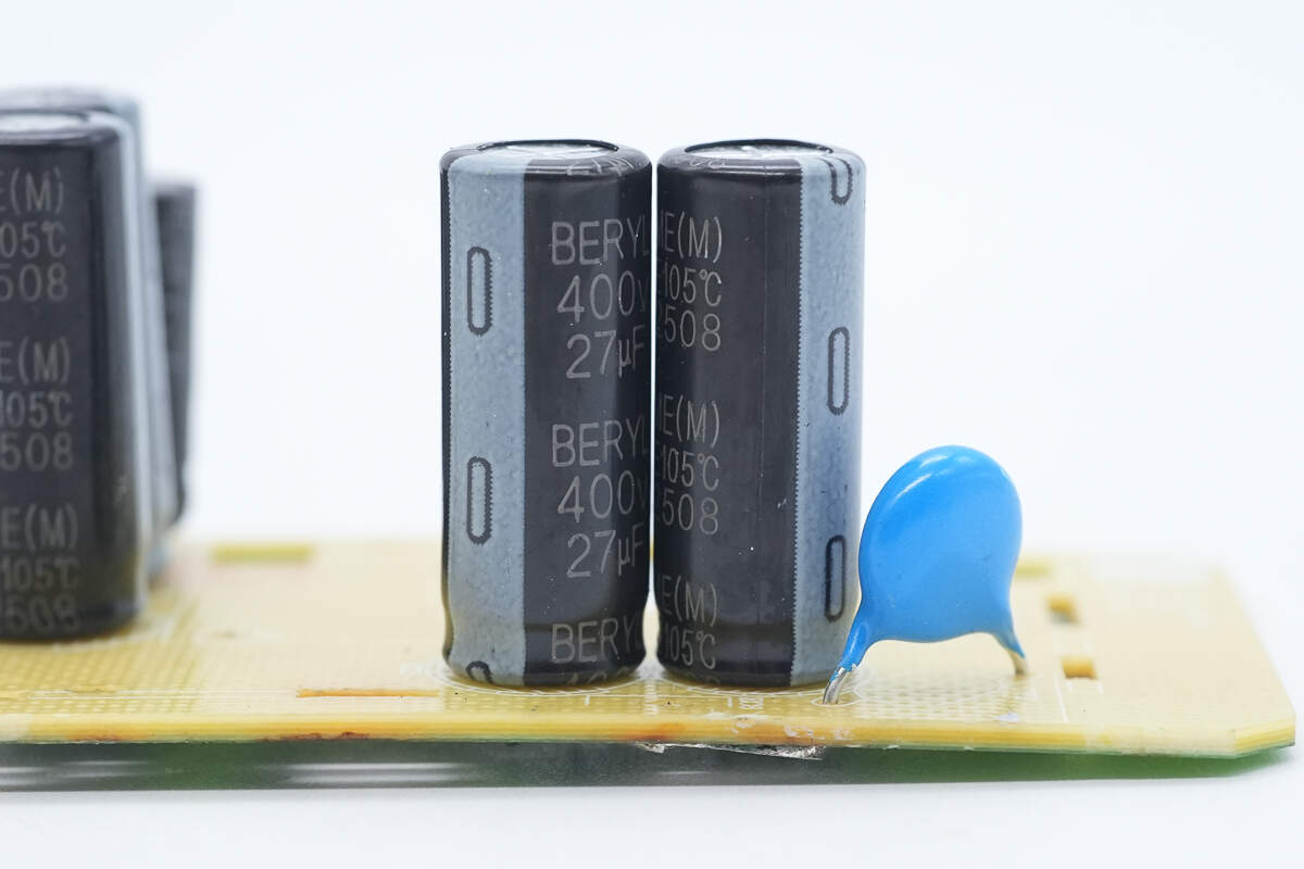
These two electrolytic capacitors are also from BERYL, both rated at 400V 27μF.
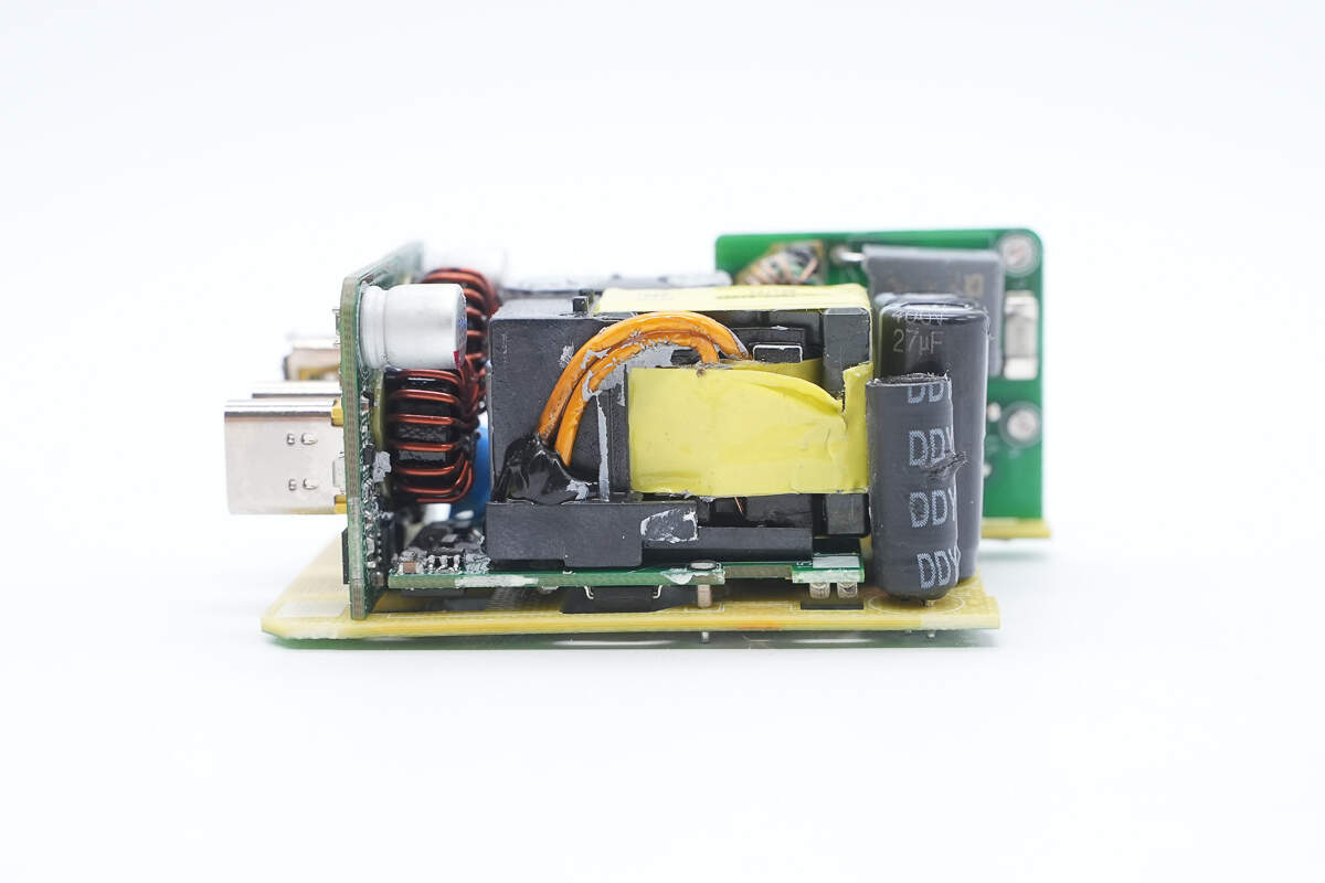
On the other side is the AC-DC standard modular PCBA. This module integrates the AC-DC power conversion components into a standardized unit, which can serve as a 65W module compatible with various device models. It mainly includes the primary integrated GaN chip, transformer, synchronous rectification, output solid-state components, an output 431-volt regulation circuit, and primary-to-secondary optocouplers, along with other peripheral components.
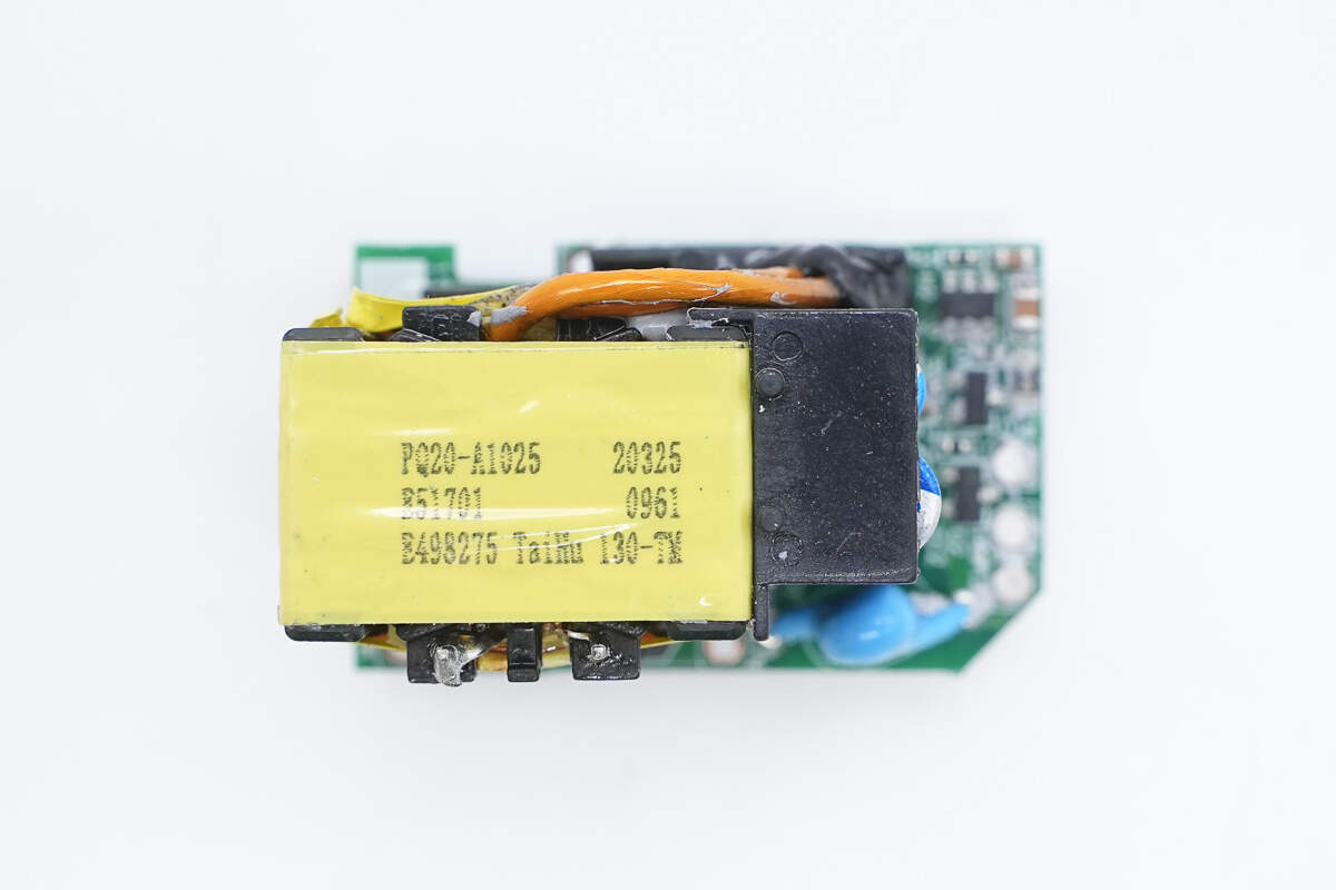
The transformer is soldered to the small PCB at the bottom. On the right side of the PCB, there are blue Y capacitors, a synchronous rectifier controller, and solid capacitors for output filtering.
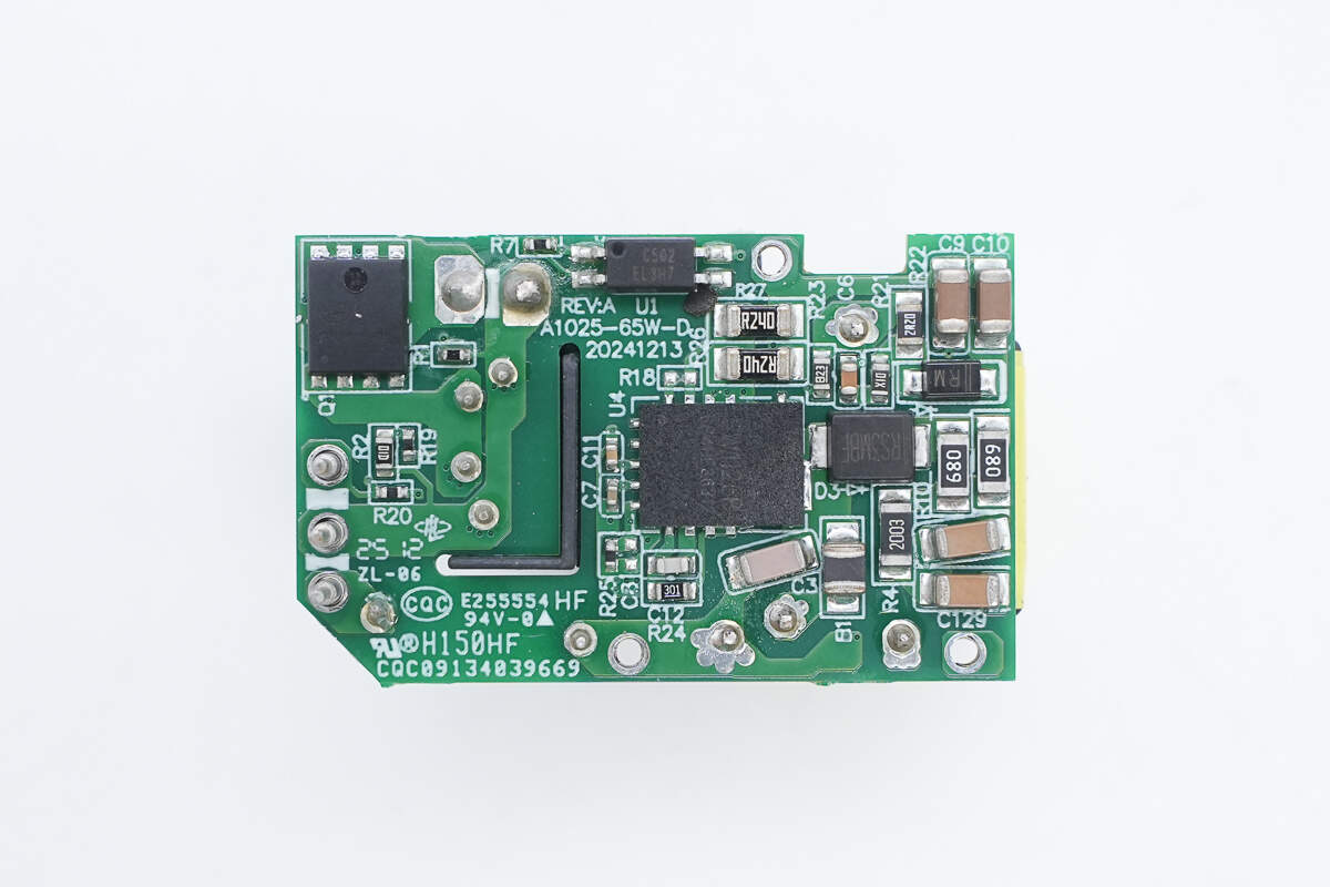
On the back of the PCB, there is the master control chip, an optocoupler, and the synchronous rectifier.
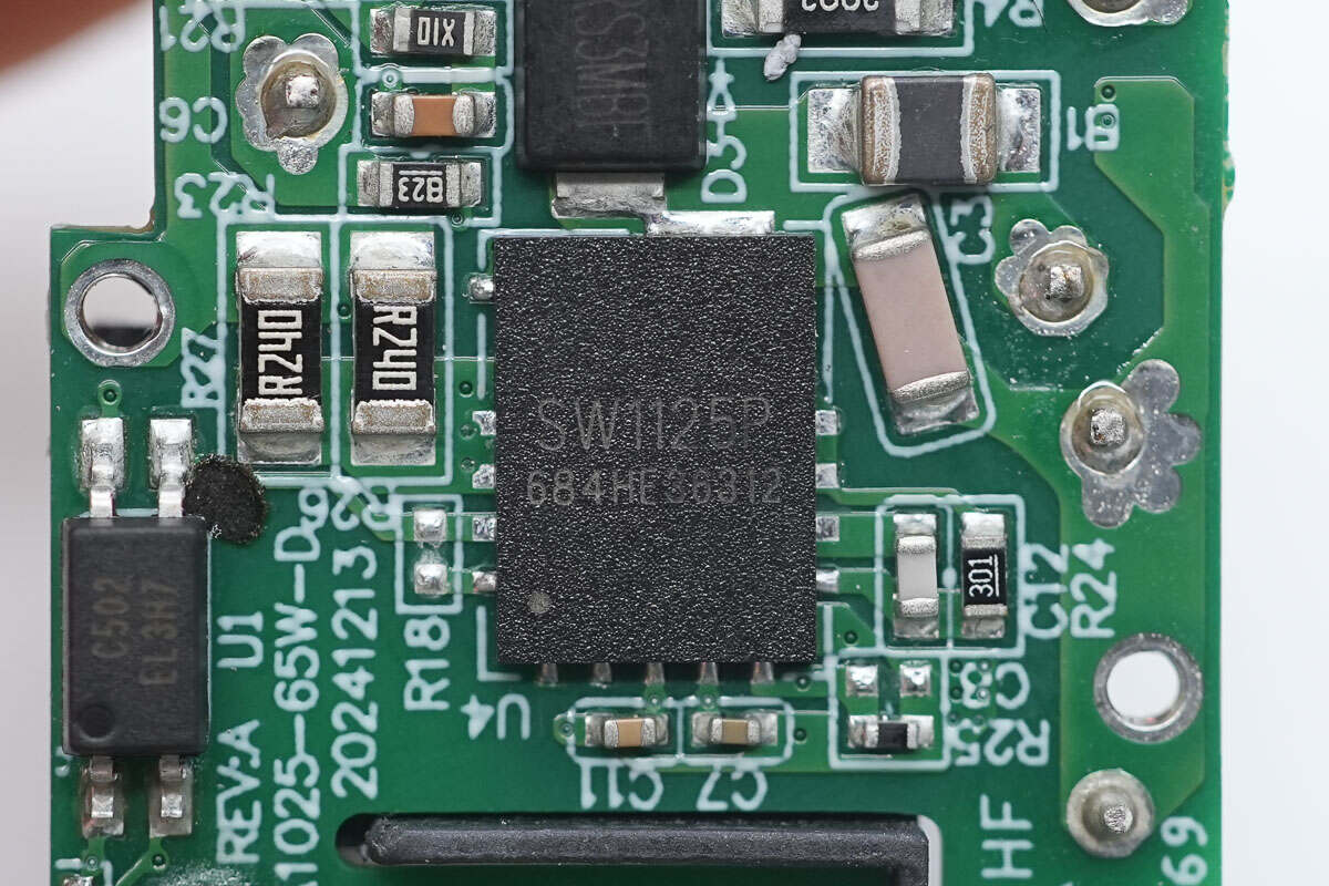
The master control chip is the iSmartWare SW1125P integrated GaN chip. This chip features a 650V withstand voltage and a 260mΩ on-resistance GaN FET in a high-frequency quasi-resonant flyback converter. It also integrates a 700V high-voltage startup circuit, line voltage dropout detection, and X-capacitor discharge functionality.
The SW1125P operates in valley-fill locked valley turn-on mode to reduce switching losses and includes frequency dithering to optimize EMI performance. It supports burst mode, automatically entering burst mode at light loads to improve efficiency. Its no-load standby power consumption is under 50mW, meeting Level 6 energy efficiency standards.
The SW1125P supports an ultra-wide input voltage range of 8–90V and a maximum switching frequency of up to 300kHz. It uses a thermally enhanced QFN 6×8 package, allowing heat dissipation through vias to reduce chip temperature, optimize PCB layout, and simplify thermal design. The chip includes multiple comprehensive protection features and supports an external NTC thermistor to monitor charger temperature, ensuring full protection coverage.
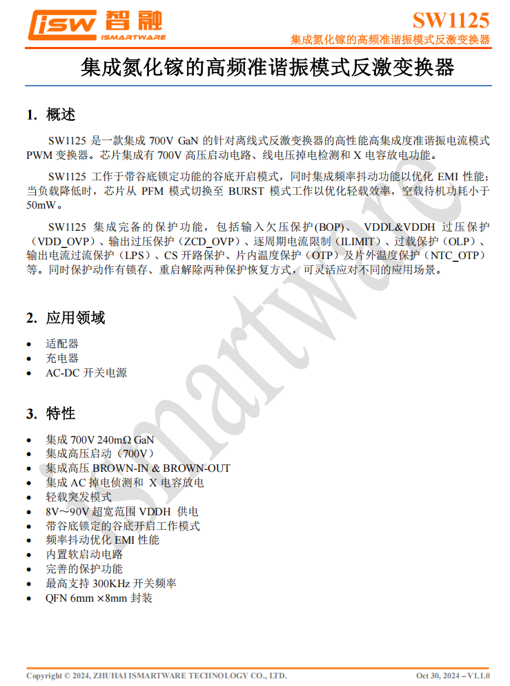
Close-up of the transformer.
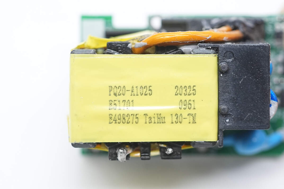
The Everlight EL 3H7 optocoupler is used for output voltage feedback.
Close-up of the blue Y capacitor.
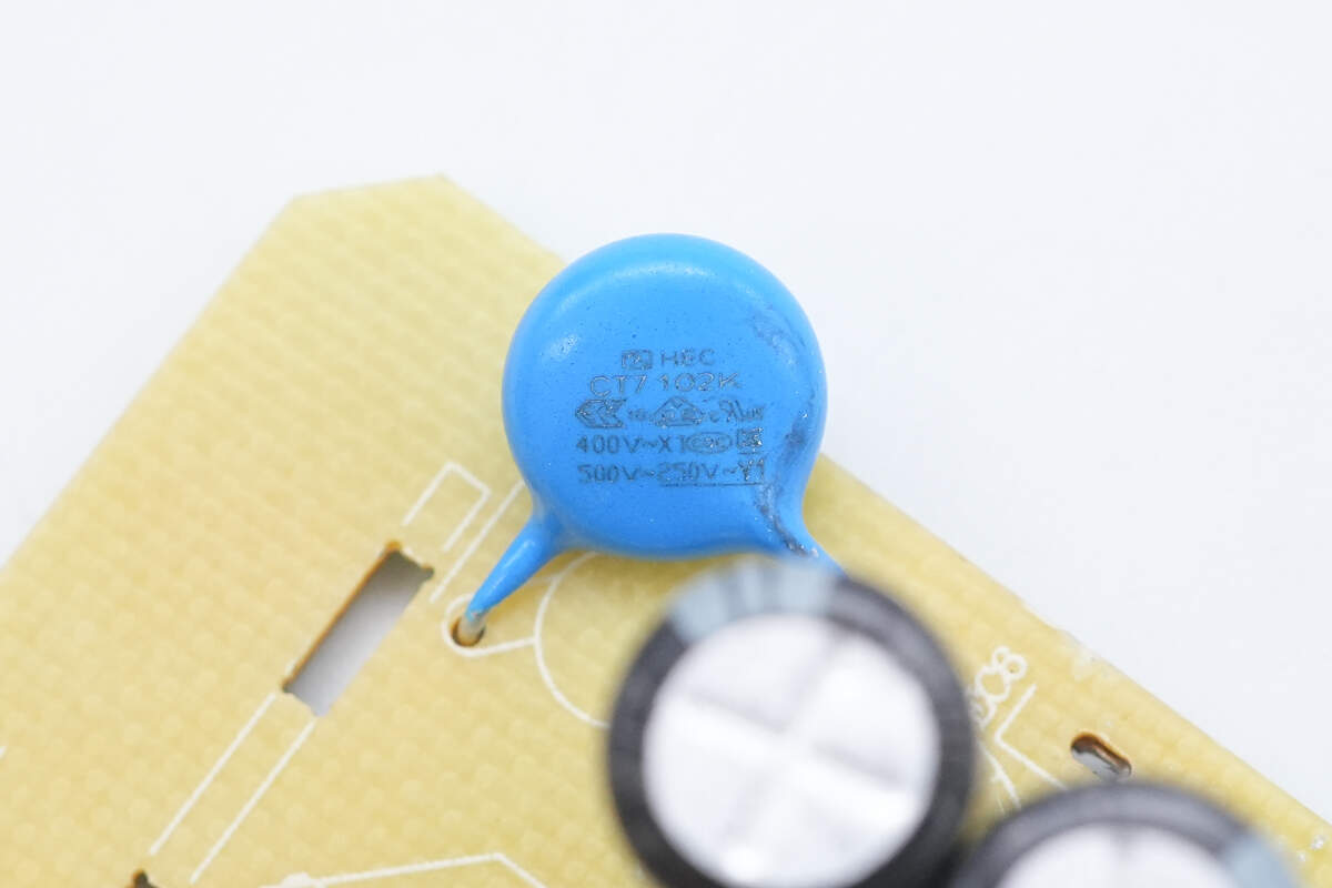
Close-up of the other blue Y capacitor.
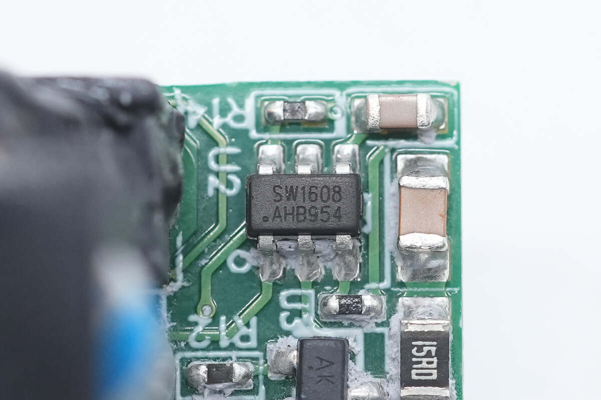
The synchronous rectifier controller uses the iSmartWare SW1608, a high-performance controller designed for secondary-side synchronous rectifier driving in offline flyback converters. It comes in an SOT23-6 package and supports a 6V or 9V VCC power supply. The VCC features a self-powering function, eliminating the need for an auxiliary winding and supporting a wide output voltage range. When paired with a MOSFET to replace the Schottky rectifier diode, it can significantly improve system efficiency.
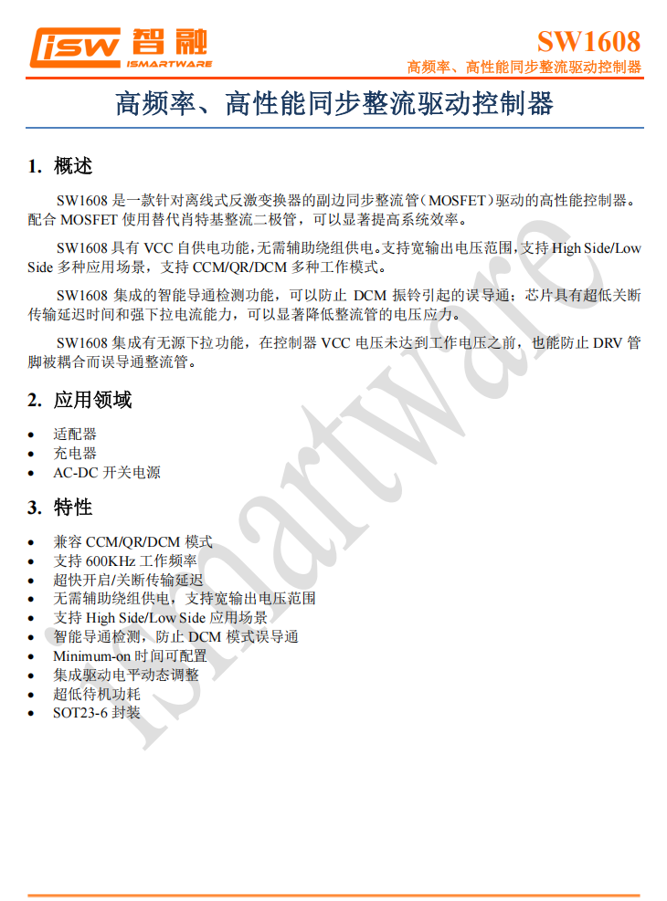
The SW1608 supports operating frequencies up to 600kHz and is compatible with various application scenarios, including High Side and Low Side configurations. It supports multiple working modes such as CCM, QR, and DCM. Additionally, it features an intelligent conduction detection function to effectively prevent false conduction caused by DCM ringing. The chip also boasts ultra-low turn-off propagation delay and strong pull-down current capability, which significantly reduces the voltage stress on the rectifier MOSFET.
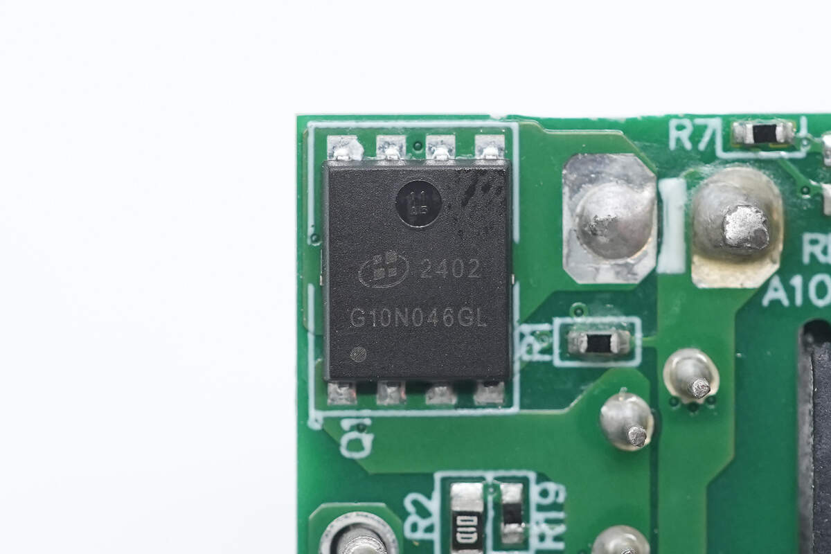
The synchronous rectifier is from ALKAIDSEMI, model AKG10N046GL. It is an N-channel MOSFET with a 100V voltage rating and 4.6mΩ on-resistance, housed in a PDFN 5×6-8L package.
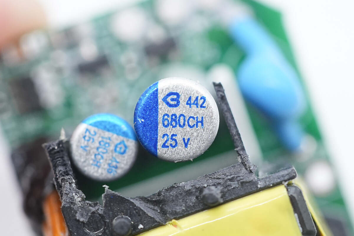
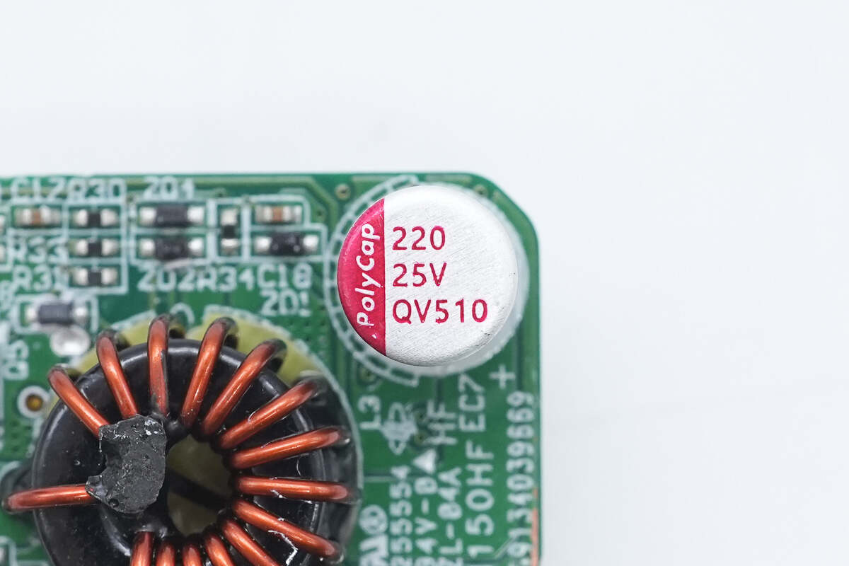
The solid capacitor used for output filtering is from BERYL, rated at 25V 680μF.
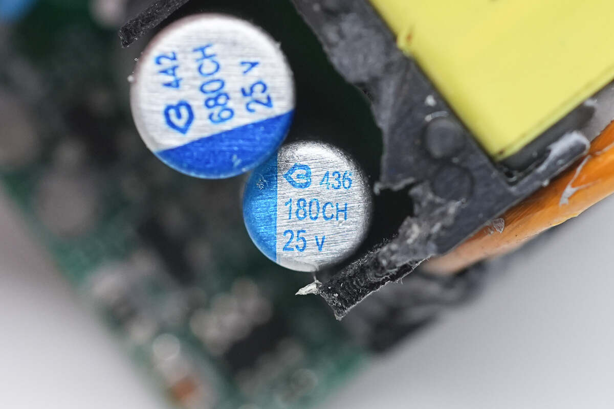
The other solid capacitor is rated at 25V 180μF.
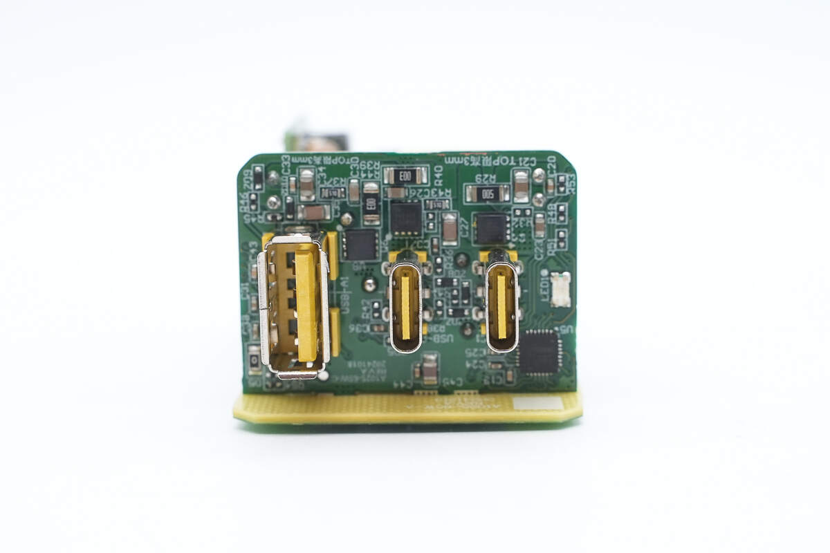
The front of the small PCB at the output end is equipped with the USB-C1 buck protocol chip, three USB sockets, and their corresponding VBUS MOSFETs.
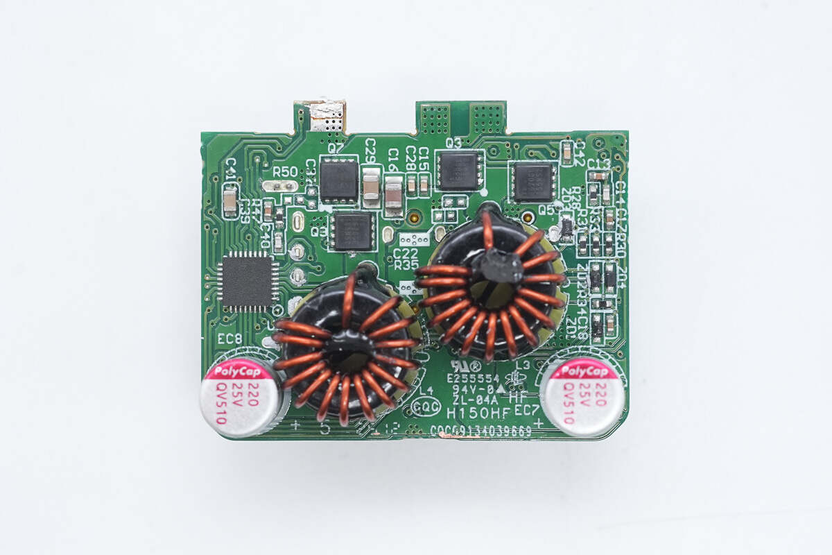
On the back side, there is another buck protocol chip for the USB-A and USB-C ports, along with synchronous buck MOSFETs for the two buck circuits, buck inductors, and secondary filtering solid capacitors.
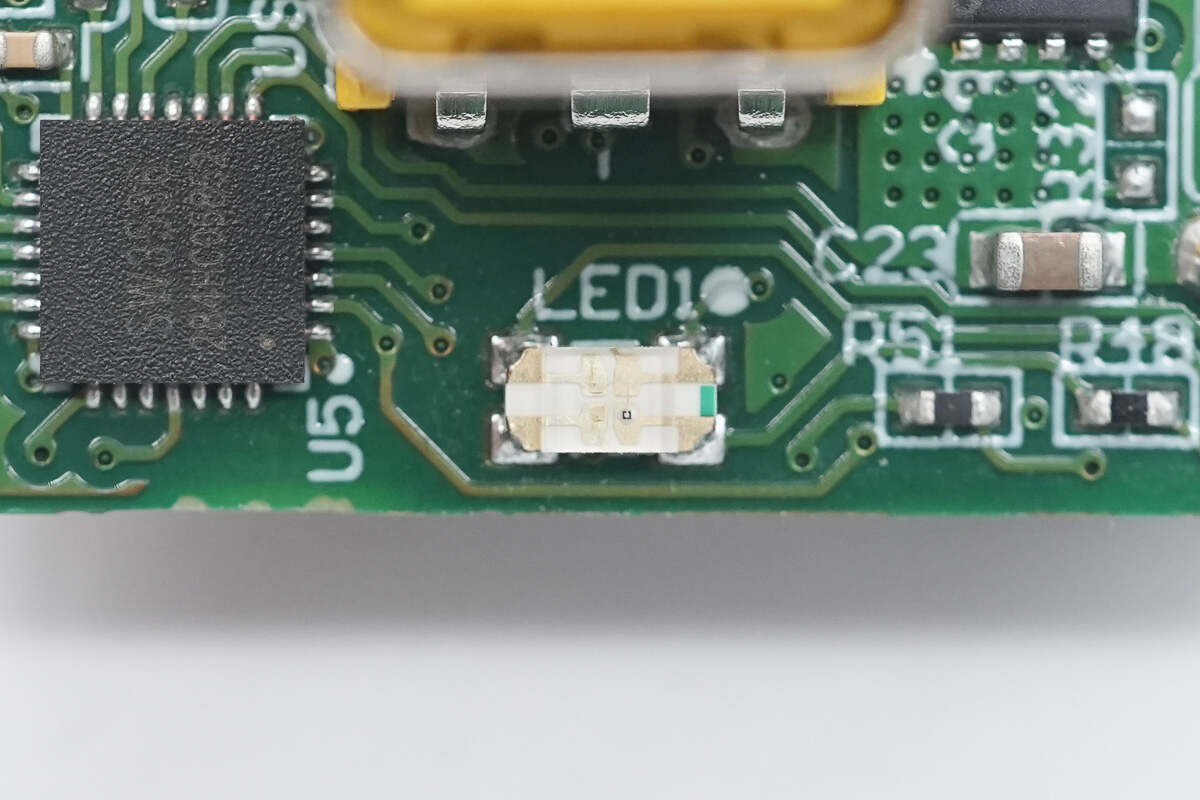
Close-up of the LED indicator light.
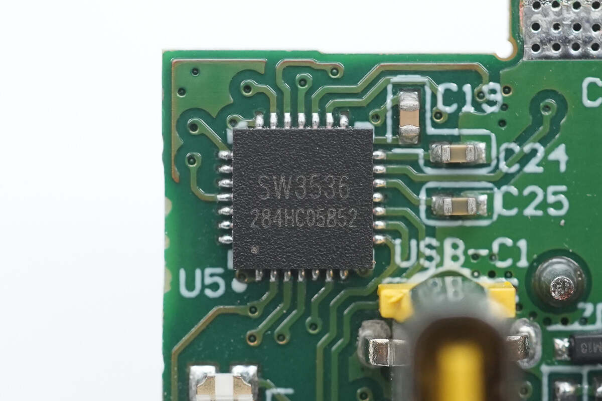
The USB-C1 buck protocol chip is the iSmartWare SW3536, a highly integrated dual-port fast charging chip that supports USB-A + USB-C simultaneous fast charge output with independent current limiting for each port. It features a built-in 7A high-efficiency synchronous buck converter and supports a wide range of fast charging protocols, including PPS, PD, QC, AFC, FCP, SCP, PE, SFCP, and TFCP. The chip supports a maximum output power of up to 140W.
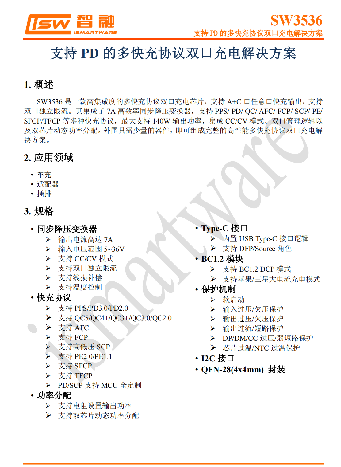
The SW3536 integrates CC/CV control, dual-port management logic, and dual-chip dynamic power distribution. With minimal external components, it provides a complete high-performance solution for multi-protocol dual-port fast charging. It supports input voltages up to 36V, making it suitable for 12–24V car charger applications. The chip is ideal for fast charging adapters, power strips, and car chargers.
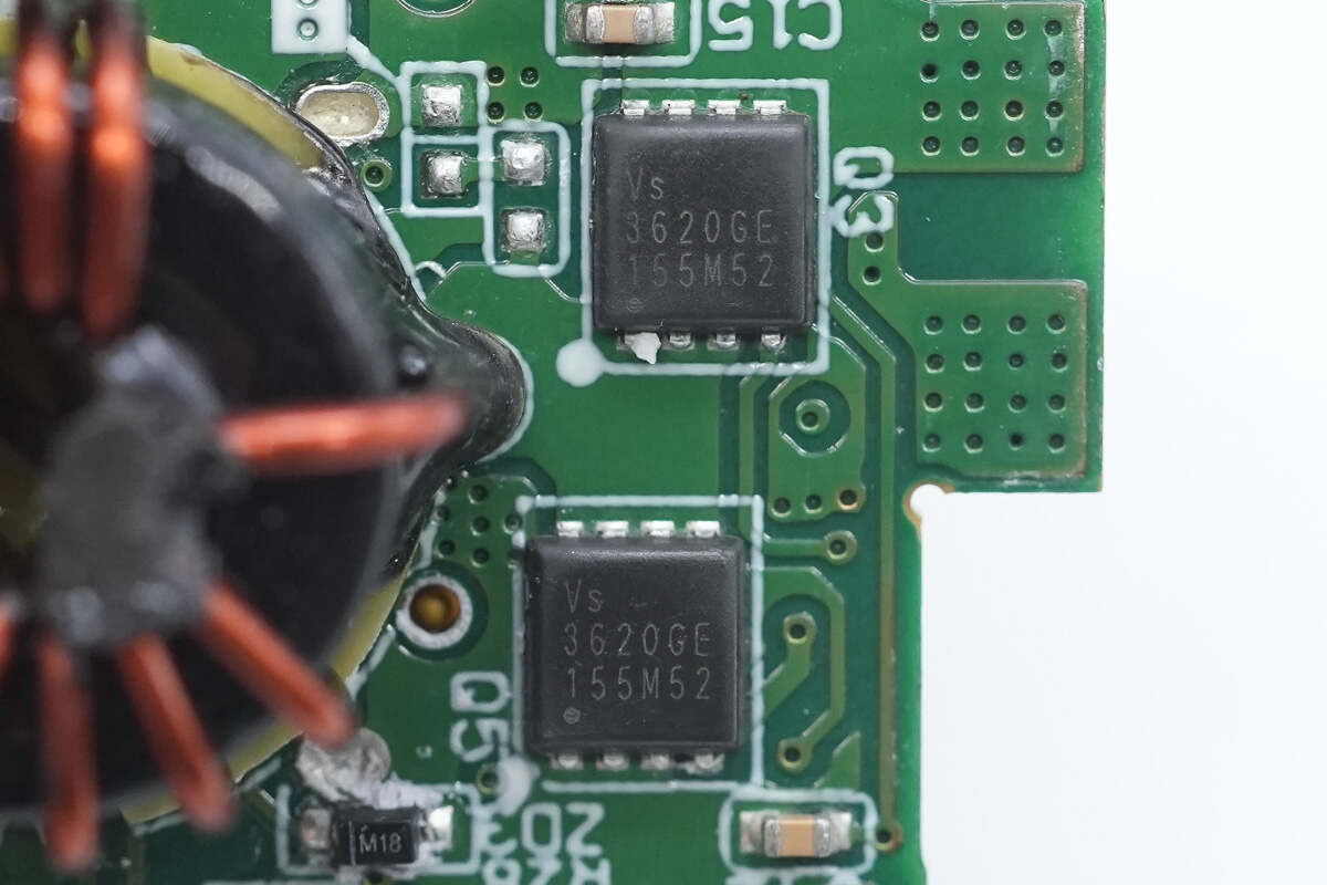
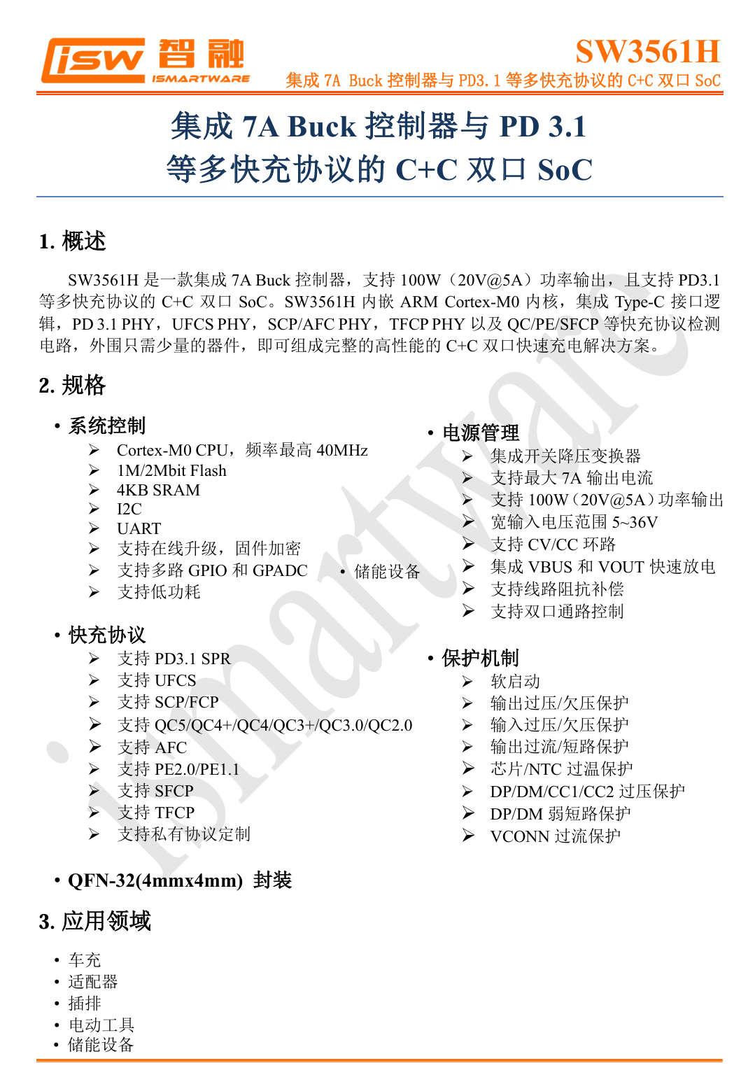
The two synchronous buck MOSFETs used with the SW3536 are from Vergiga, model VS3620GEMC. These are N-channel MOSFETs rated at 30V with an on-resistance of 4.9mΩ, housed in a PDFN3333 package. Two of them are configured as a half-bridge for synchronous buck conversion.
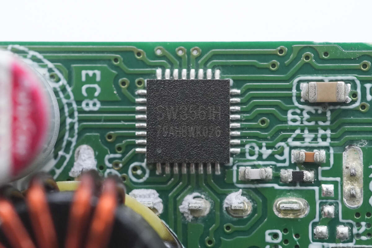
The other buck protocol chip is the iSmartWare SW3561H, a buck SoC that supports dual USB-C output. It integrates a high-efficiency synchronous buck controller and supports up to 20V 5A power output, with compatibility for USB PD3.1 SPR. The chip features a built-in ARM Cortex-M0 core and integrated Type-C logic. It supports a wide range of fast charging protocols, including PD3.1, QC, SCP, and UFCS fusion fast charging, and also allows for custom fast charge protocol configurations.
The iSmartWare SW3561H supports dual USB-C path control and includes line loss compensation. When paired with two synchronous buck MOSFETs and VBUS MOSFETs for each port, it enables dual-port buck output. The chip’s built-in buck converter has a default operating frequency of 180kHz, with support for customizable switching frequencies. It supports up to 100W power output, making it ideal for compact designs. The SW3561H features comprehensive protection mechanisms, including over-temperature protection, input/output overvoltage, and undervoltage protection, output overcurrent protection, and data line overvoltage protection. It comes in a QFN-32 package.
Here is the information about iSmartWare SW3561H.
The two synchronous buck MOSFETs paired with it are also Vergiga VS3620GEMC models.
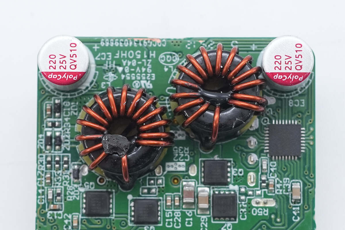
The buck inductors for both buck circuits have bakelites at the bottom and are reinforced with adhesive glue.
The secondary filtering solid capacitors for the buck outputs of both circuits are from Berykai, each rated at 25V 220μF.
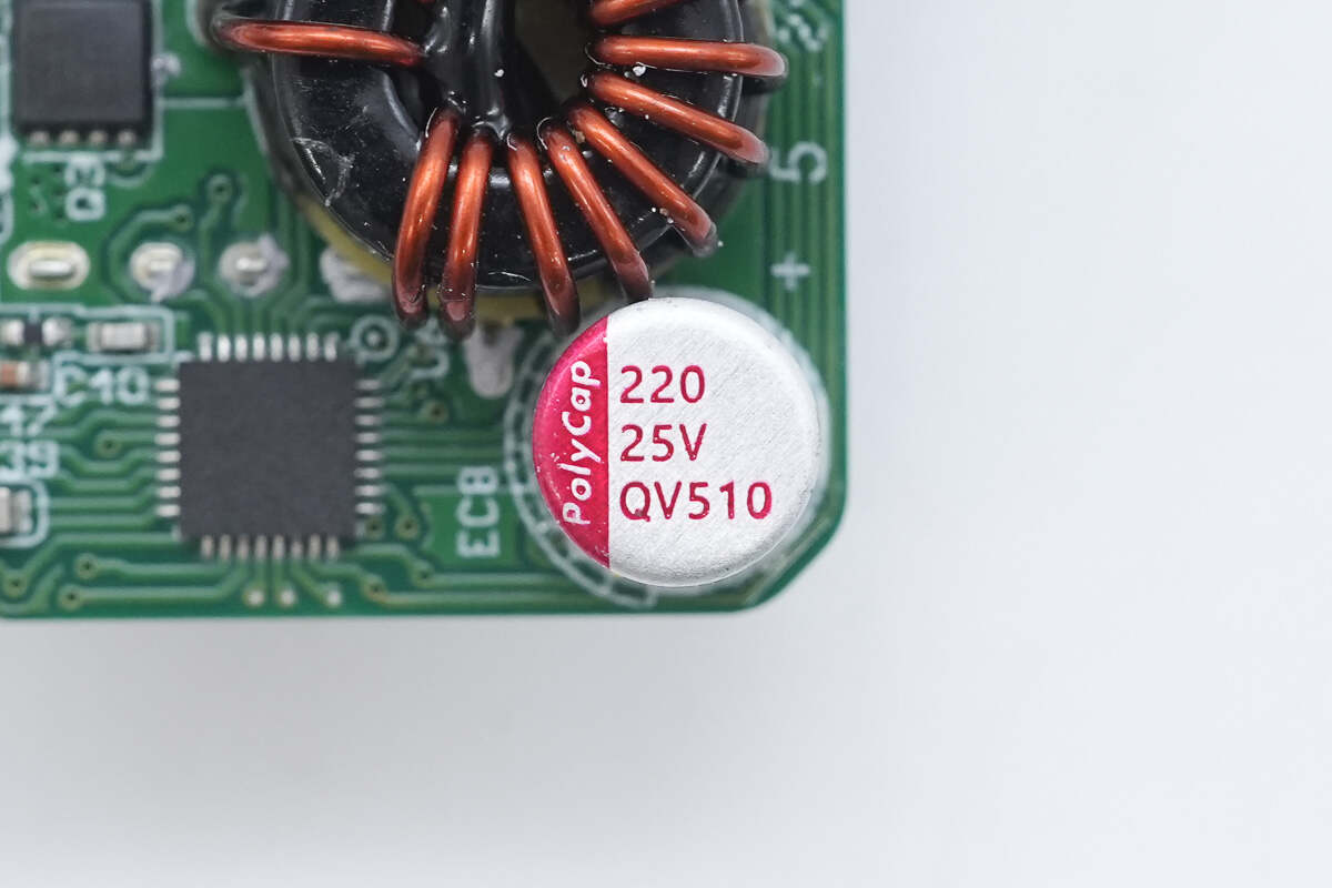
The other capacitor has the same specifications: 25V 220μF.
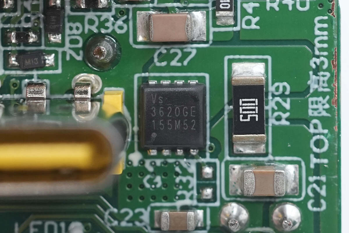
The USB-C1 VBUS MOSFET also uses the Vergiga VS3620GEMC model.
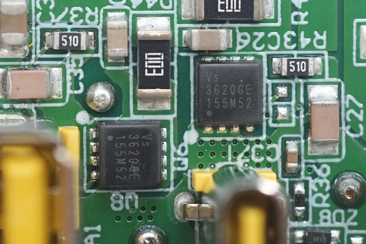
The VBUS MOSFETs for the USB-A and the other USB-C port also use the Vergiga VS3620GEMC model.
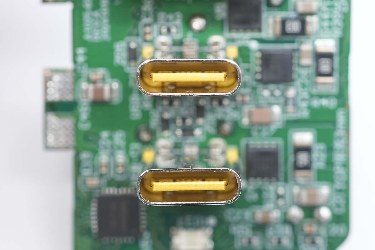
Close-up of the USB-C sockets.
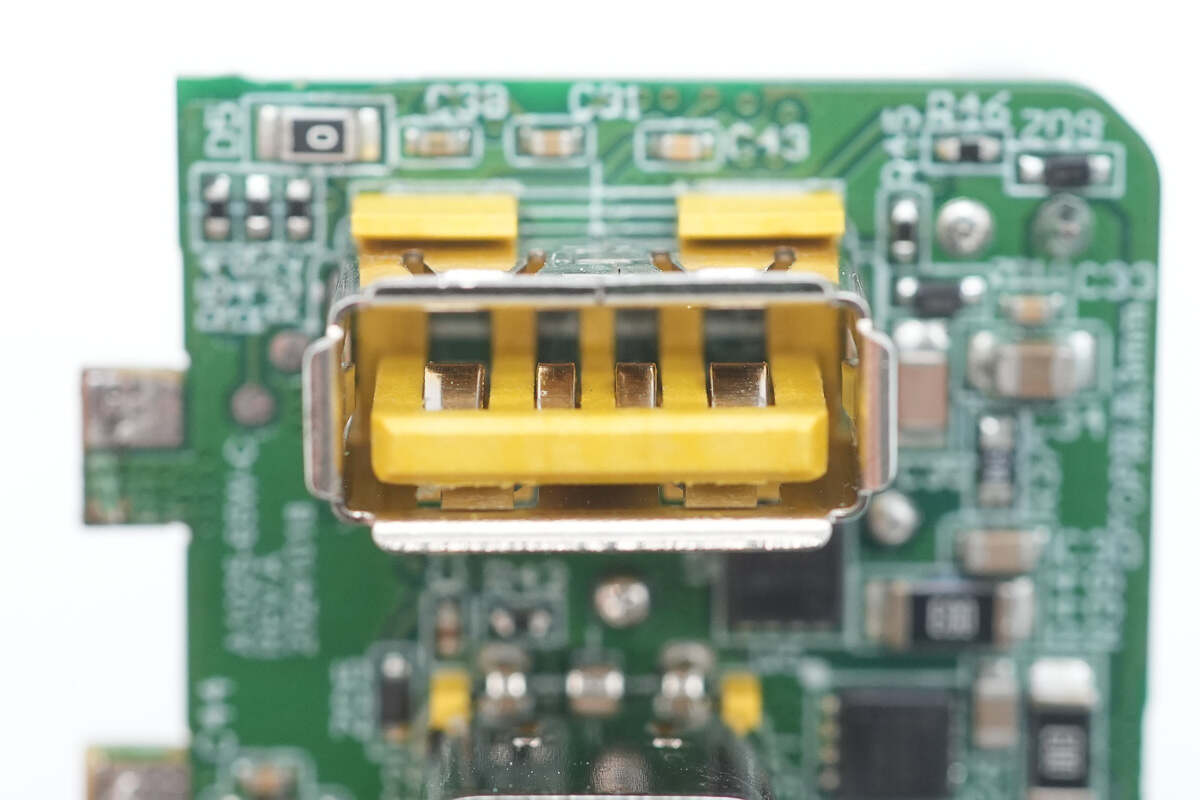
Close-up of the USB-A socket.

Well, those are all components of the AOHi The Youth PD 65W GaN 3-Port Charger.
Summary of ChargerLAB
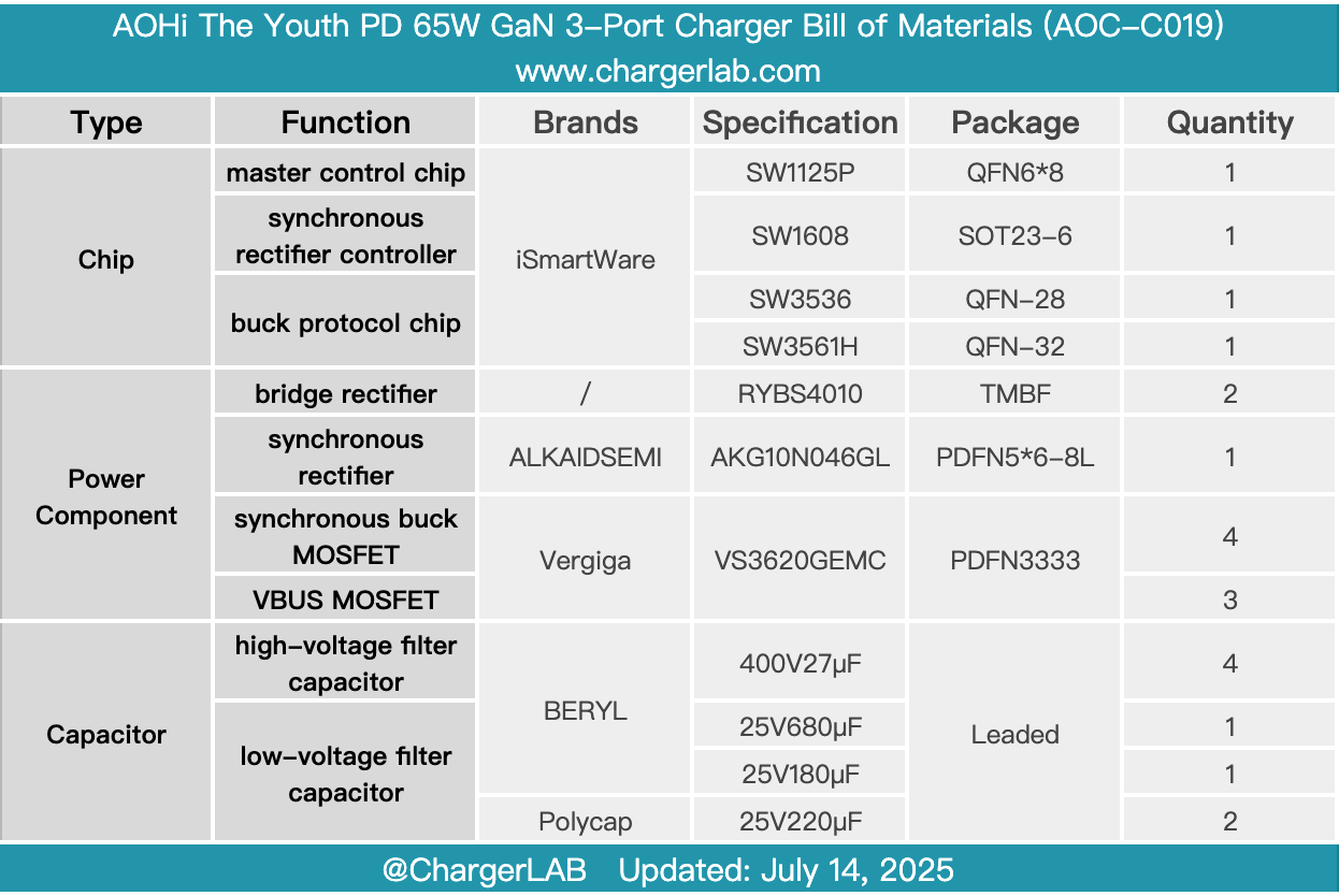
Here is the component list of the AOHi The Youth PD 65W GaN 3-Port Charger for your convenience.
It continues the design language of the same series, using yellow, blue, and green indicator lights to show charging status. The clever stacking, combined with GaN technology, enables a compact body. It supports output configurations of 45W + 20W and 30W + 30W.
After taking it apart, we found that it is designed based on the full iSmartWare fast charging solution, featuring an innovative modular design. The 65W module uses the iSmartWare SW1125P and SW1608 chips. A compact transformer helps control the module size, and it boasts high conversion efficiency, meeting temperature requirements without the need for potting. The two DC-DC circuits also use iSmartWare SW3536 and SW3561H chips for secondary buck conversion and interface output control.
The power components come from manufacturers like Vergiga, and the filtering capacitors use well-known brands such as BERYL and PolyCap. The module is filled with a substantial amount of potting compound, covering large thermal pads and heatsinks. Combined with AOHi’s ICE4.0 temperature control technology, this design enables simultaneous charging and usage without overheating, effectively protecting the health of your device’s battery.
Related Articles:
1. Teardown of UGREEN 67W 20000mAh Power Bank (PB550)
2. Teardown of Xiaomi 10000mAh 45W Power Bank with Built-in Cable and Digital Display (NPB1045)
3. Teardown of Huntkey 2000W 80 PLUS Platinum Switching Power Supply (HK2000B-S1)