Introduction
Anker previously launched a 140W four-port GaN charger. Recently, the series welcomed a new 100W model, featuring two USB-C and one USB-A port. The two USB-C ports support 100W fast charging, and all three ports support intelligent power distribution. It supports Xiaomi's 90W proprietary protocol, with both USB-C ports capable of delivering a maximum output of 90W for Xiaomi phones and tablets.
It is equipped with a screen that can display the power of all three ports. Through touch button operation, users can rotate the screen orientation, switch the displayed power, and show the charger’s temperature, making it convenient to monitor device status. It can also record the charger's usage time and comes with an 18-month warranty.
Next, we’ll take a look at the teardown of this Anker charger to examine its internal components and design.
Product Appearance
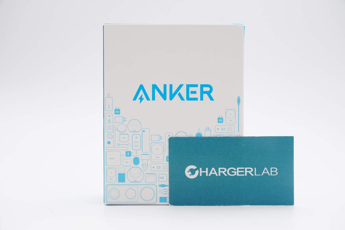
The ANKER logo is printed on the front of the box.
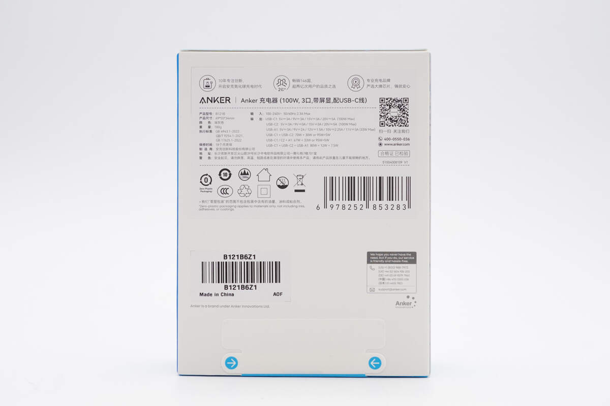
There is an information sticker on the back.
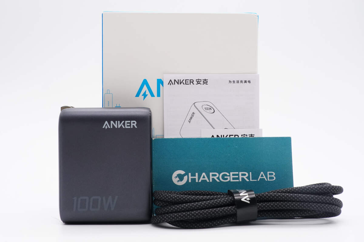
The package includes the charger, cable, and some documents.
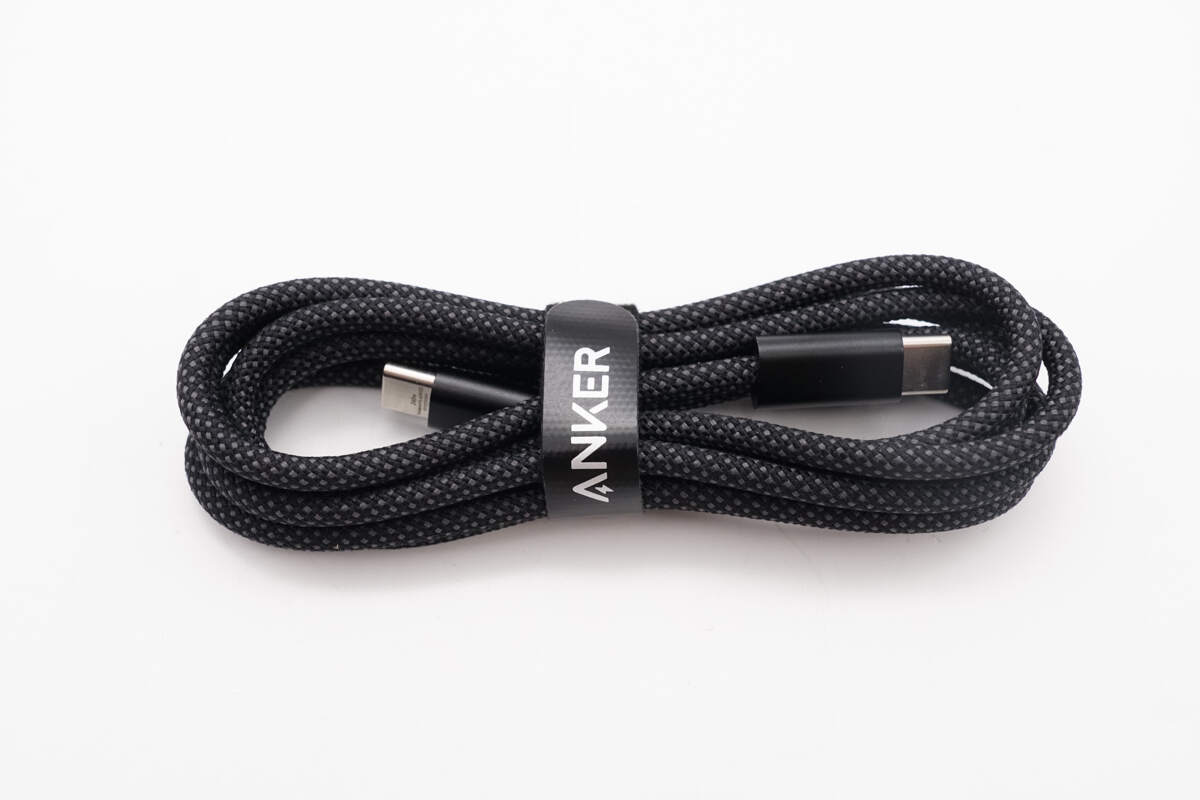
The included charging cable is a dual USB-C cable.
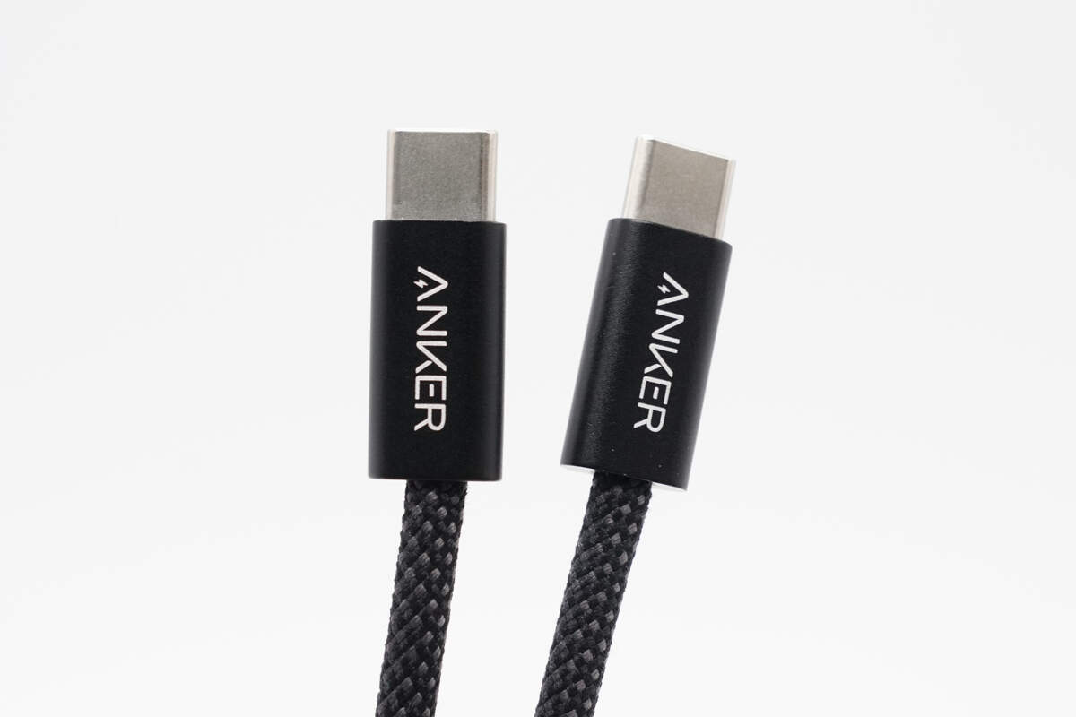
The shells of the connectors are made of aluminum alloy and printed with the ANKER logo.
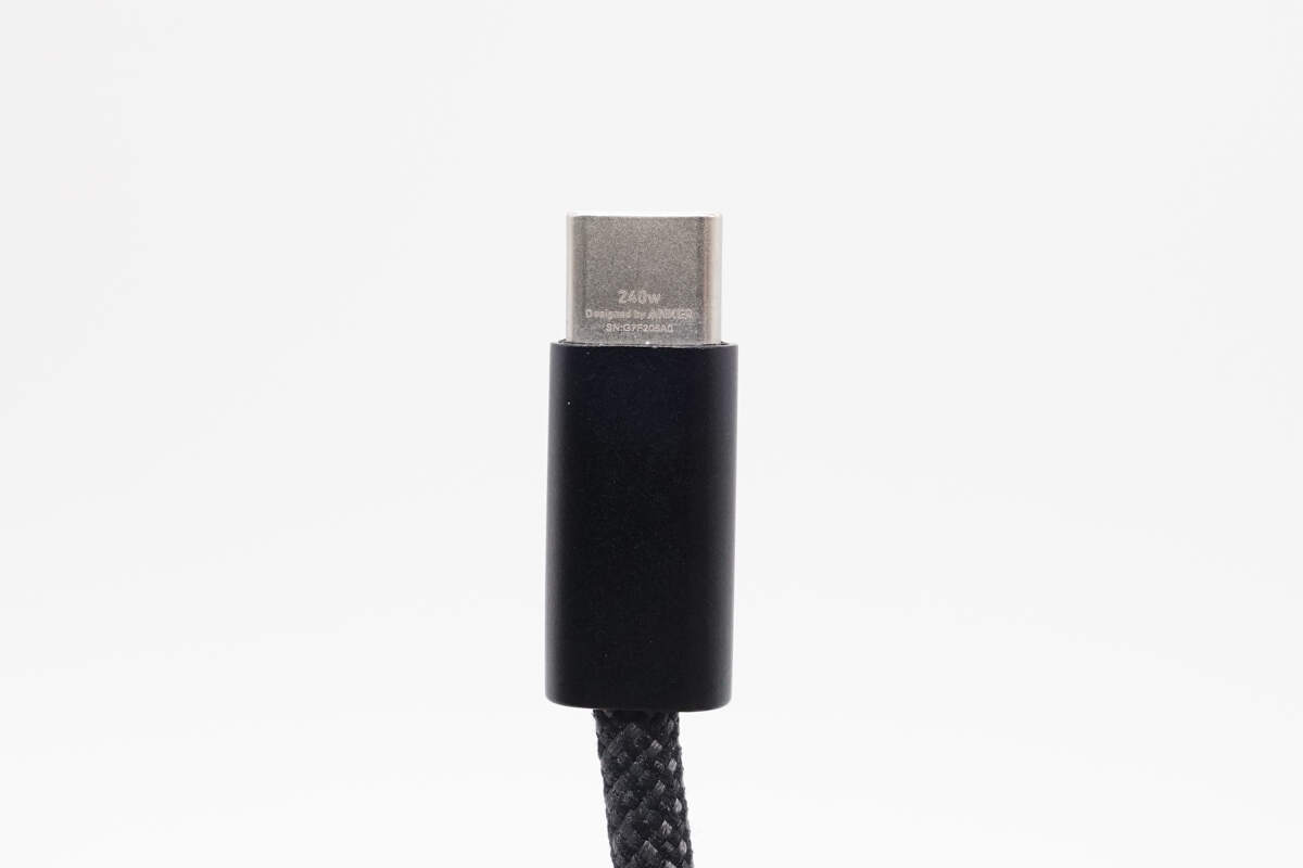
The plug is marked that it supports 240W.
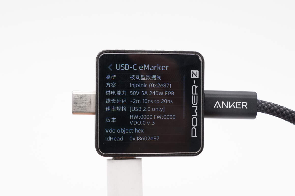
ChargerLAB POWER-Z KM003C shows it has an E-marker chip, supports 50V5A, and USB 2.0.
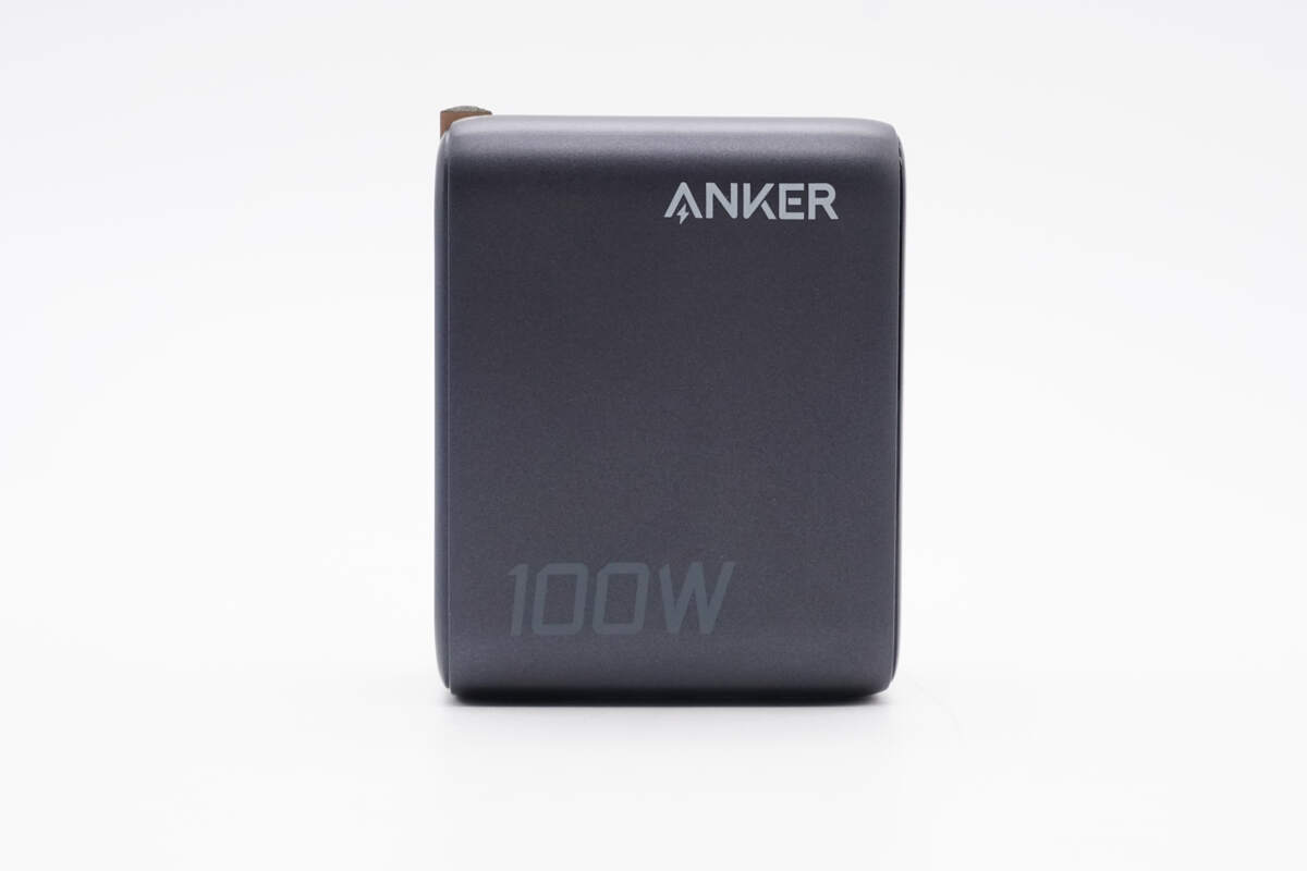
The lower left corner of the charger’s side is printed with “100W,” while the upper right corner is marked with “ANKER.”
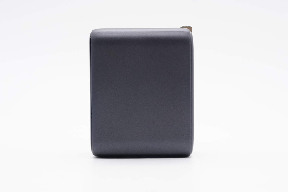
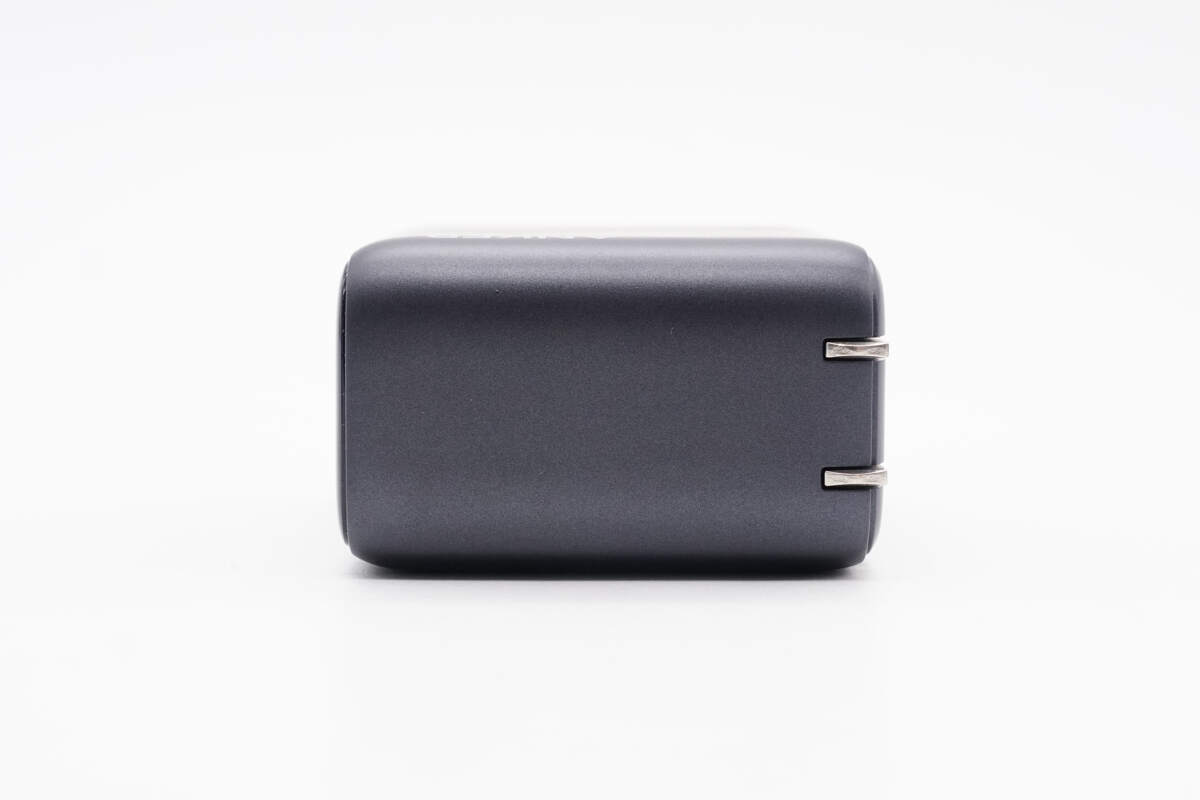
There is no marking on the other side.
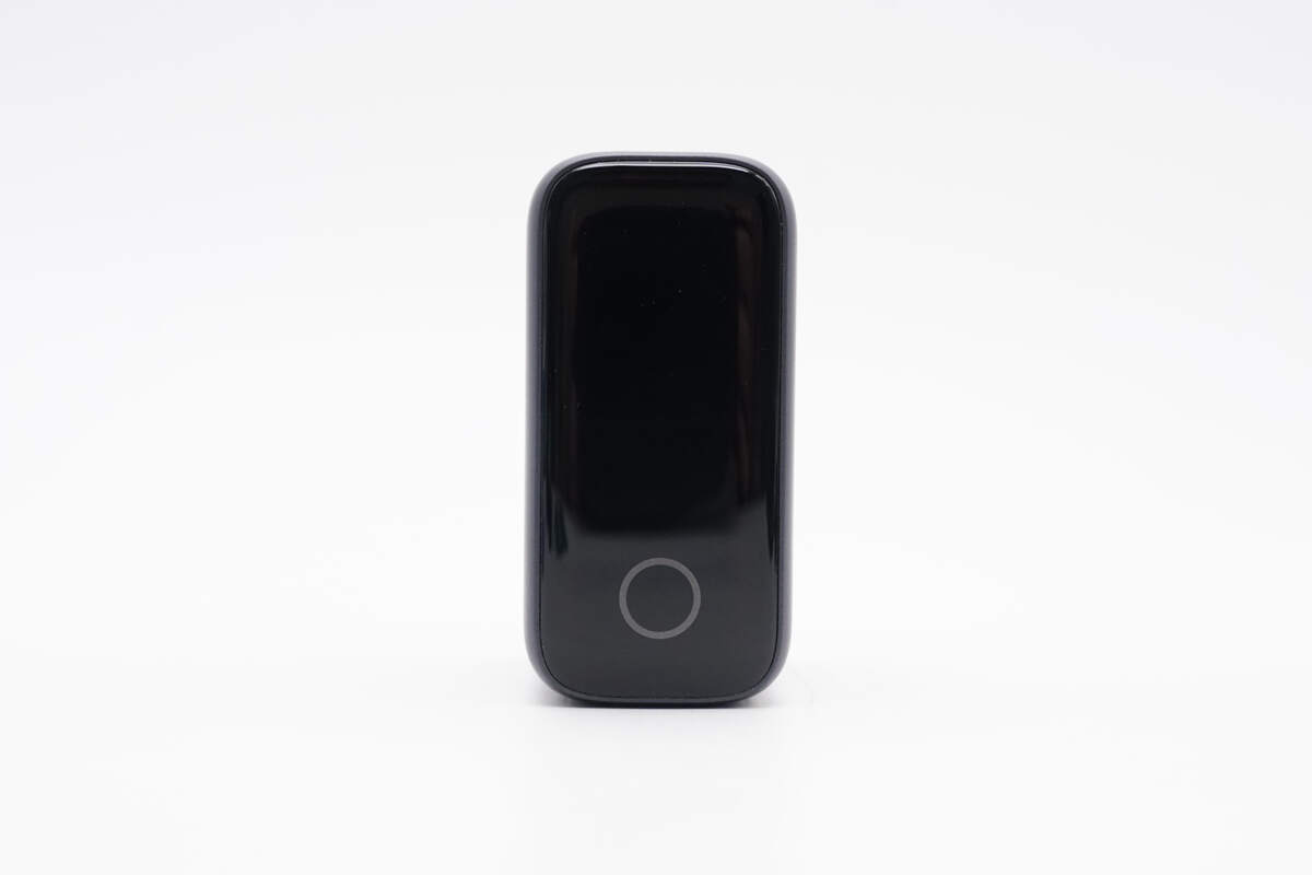
The circular area below the LCD screen contains a touch-sensitive button.
There are no markings on the top of the charger.
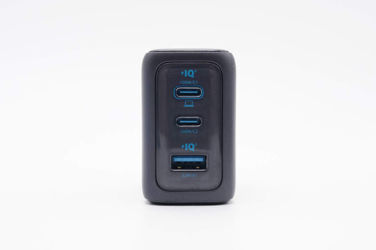
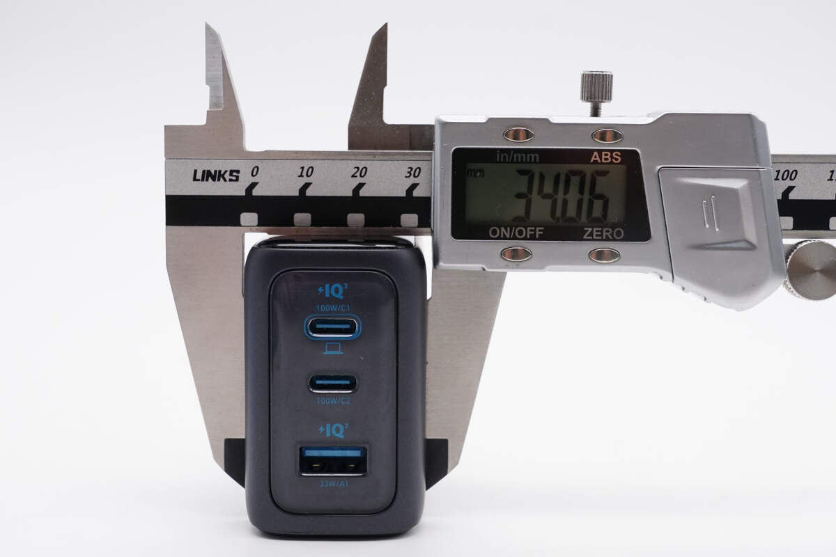
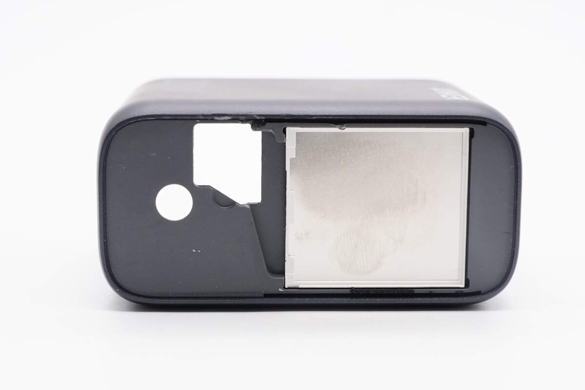
The bottom of the charger features two USB-C ports and one USB-A port.
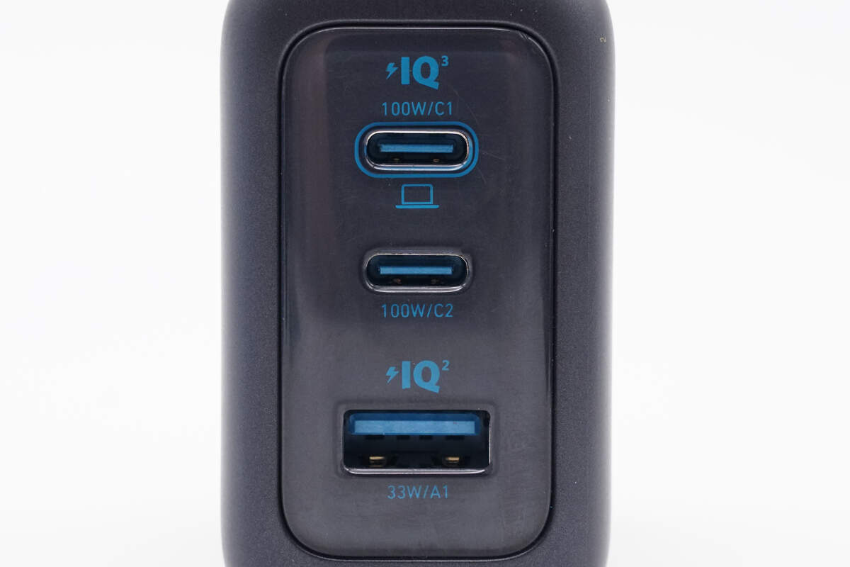
The output power ratings are labeled beneath the ports: both USB-C ports support up to 100W output, while the USB-A port supports up to 33W output.
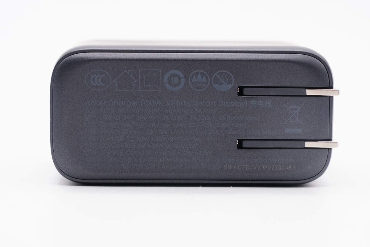
Model: A121B
Input: 100-240V\~ 50/60Hz 2.3A Max
Output:
USB-C1: 5V3A/9V3A/15V3A/20V5A(100W Max)
USB-C2: 5V3A/9V3A/15V3A/20V5A(100W Max)
USB-A1: 5V3A/9V2A/12V1.5A/10V2.25A/11V3A(33W Max)
USB-C1+USB-C2: 70W+30W or 95W+5W
USB-C1/C2+A1: 67W+33W or 95W+5W
USB-C1+USB-C2+USB-A1: 80W+12W+7.5W
Anker Innovations Technology Co., Ltd.
Designed by Anker
Made in China
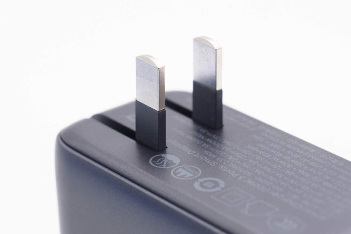
It is equipped with foldable plugs, which are fitted with insulated sleeves, significantly enhancing safety.
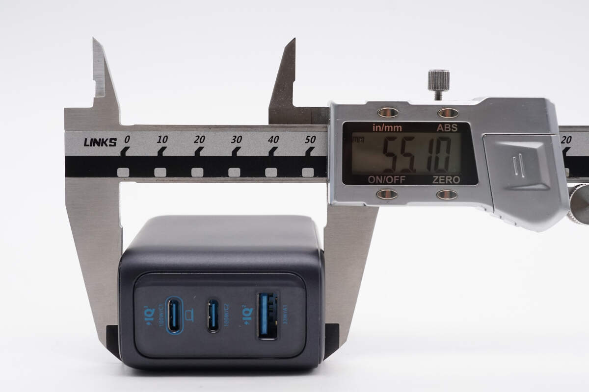
The length is about 55.1 mm (2.17 inches).
The width is about 34.1 mm (1.34 inches).
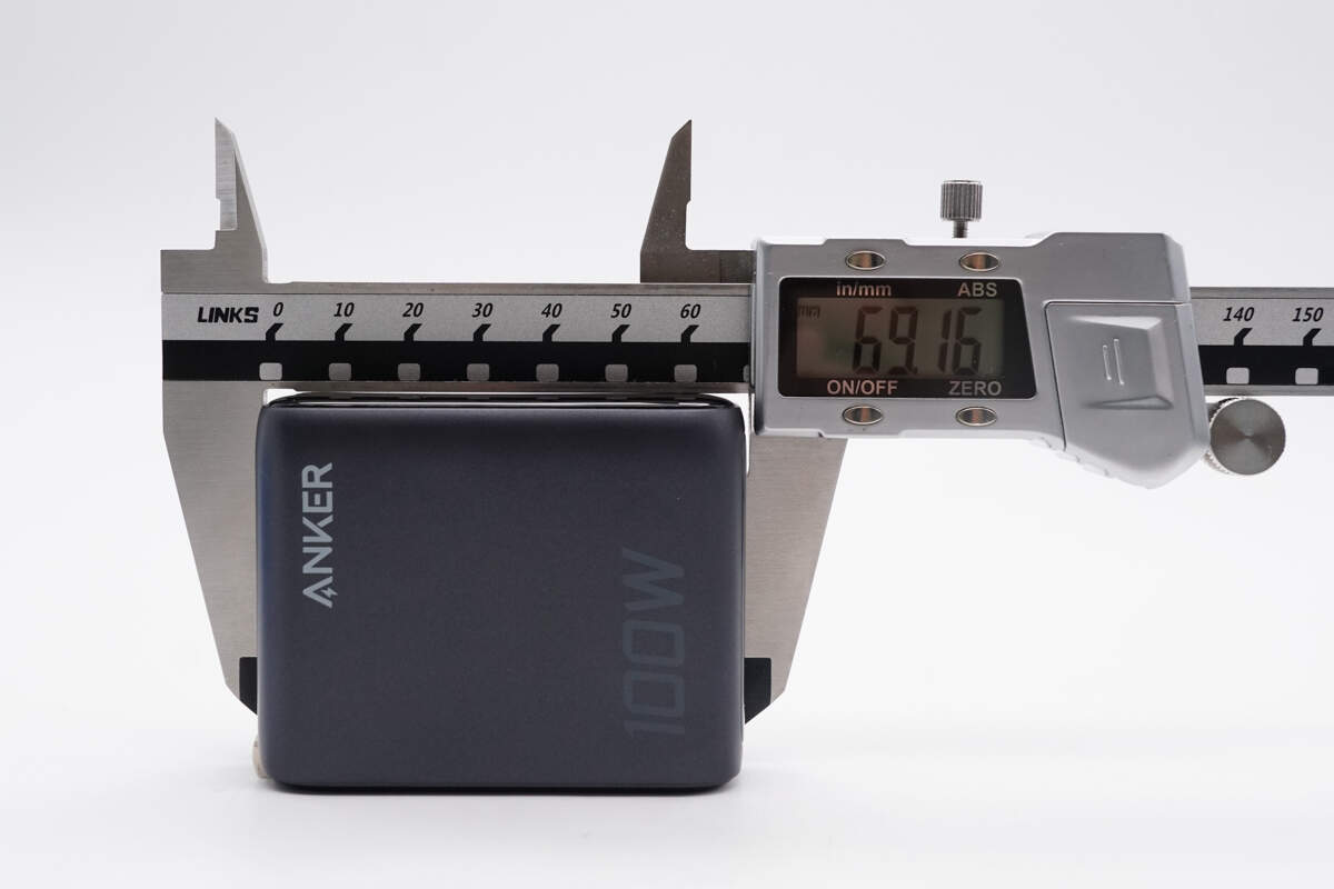
The height is about 69.2 mm (2.72 inches).
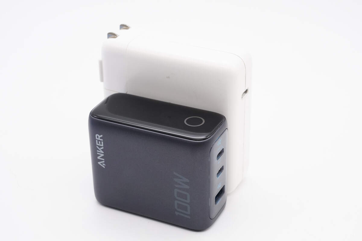
It is significantly smaller than the Apple 96W charger.
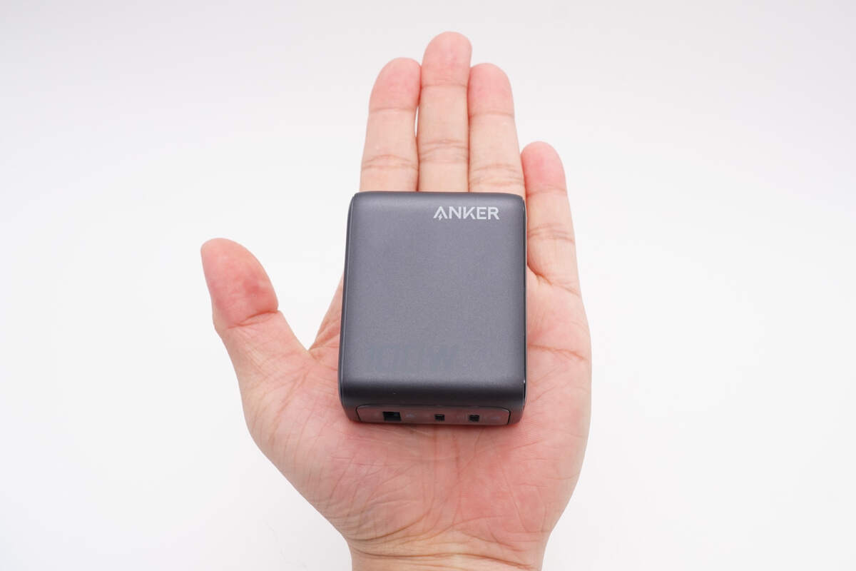
That's how big it is in the hand.
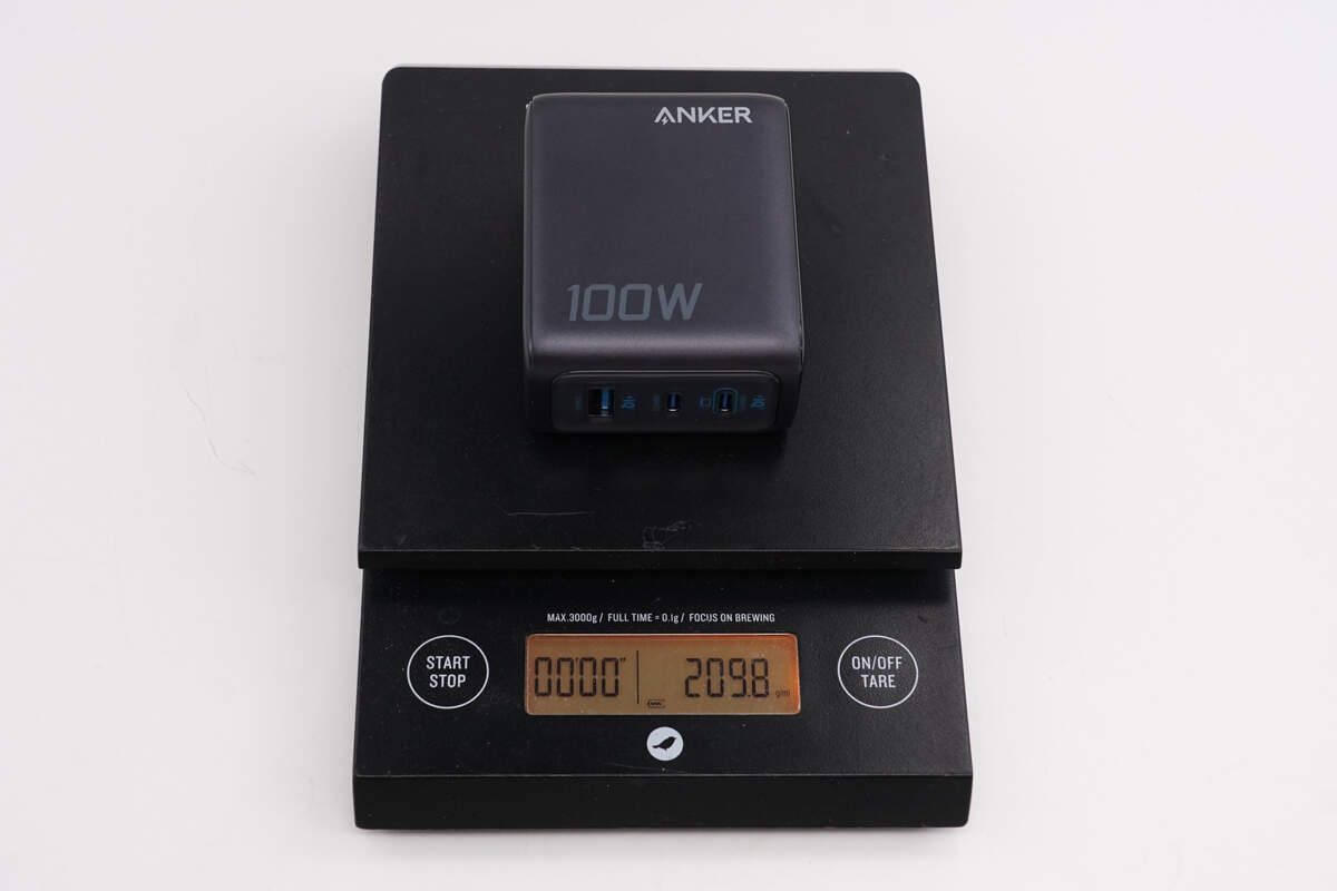
The weight is about 210 g (7.41 oz).
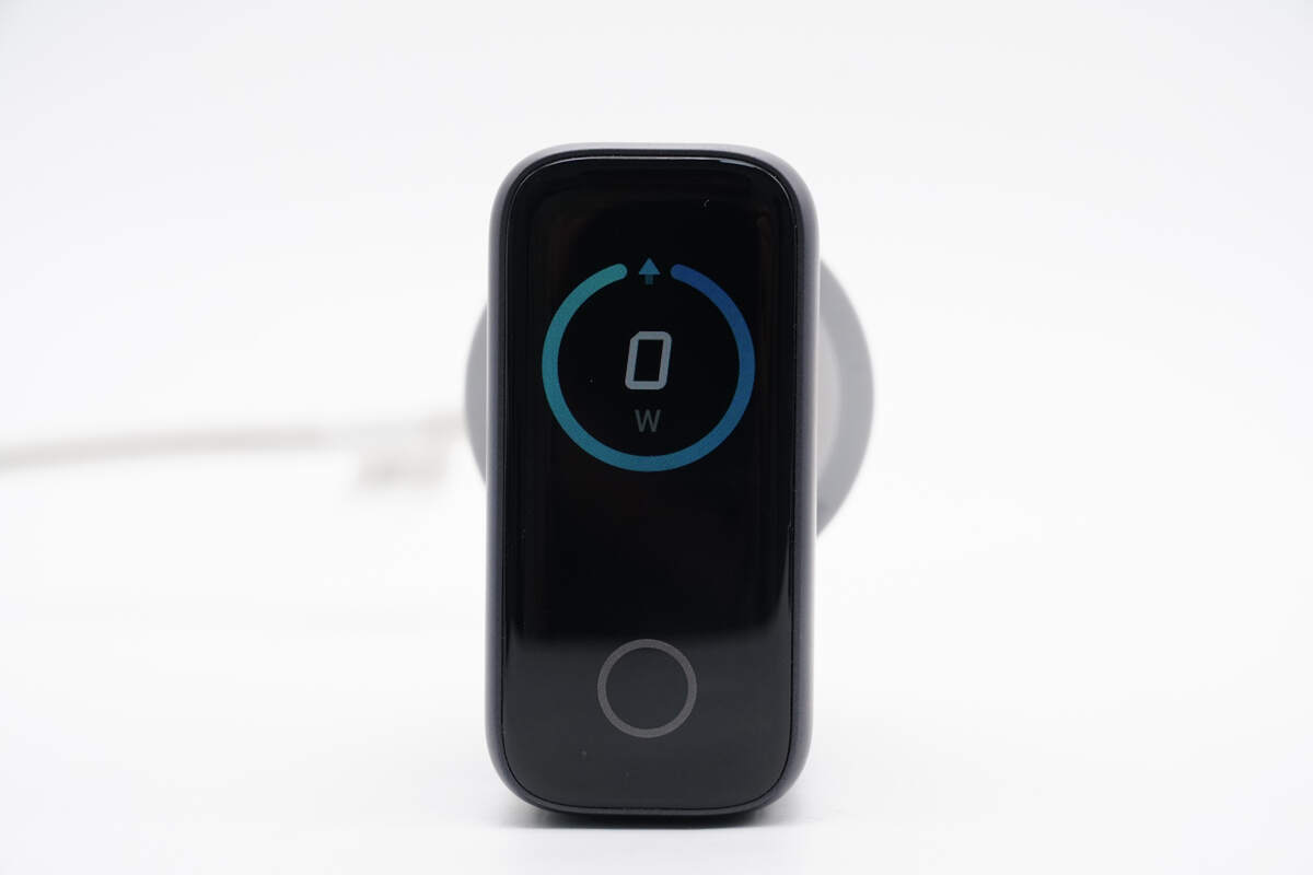
When the charger is connected to the power supply, the screen lights up and shows an output power of 0W.
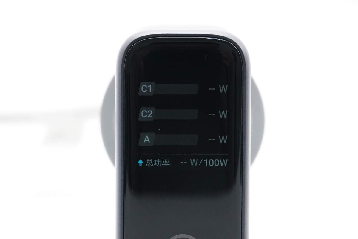
The screen can display the output power of each port and the total output power.
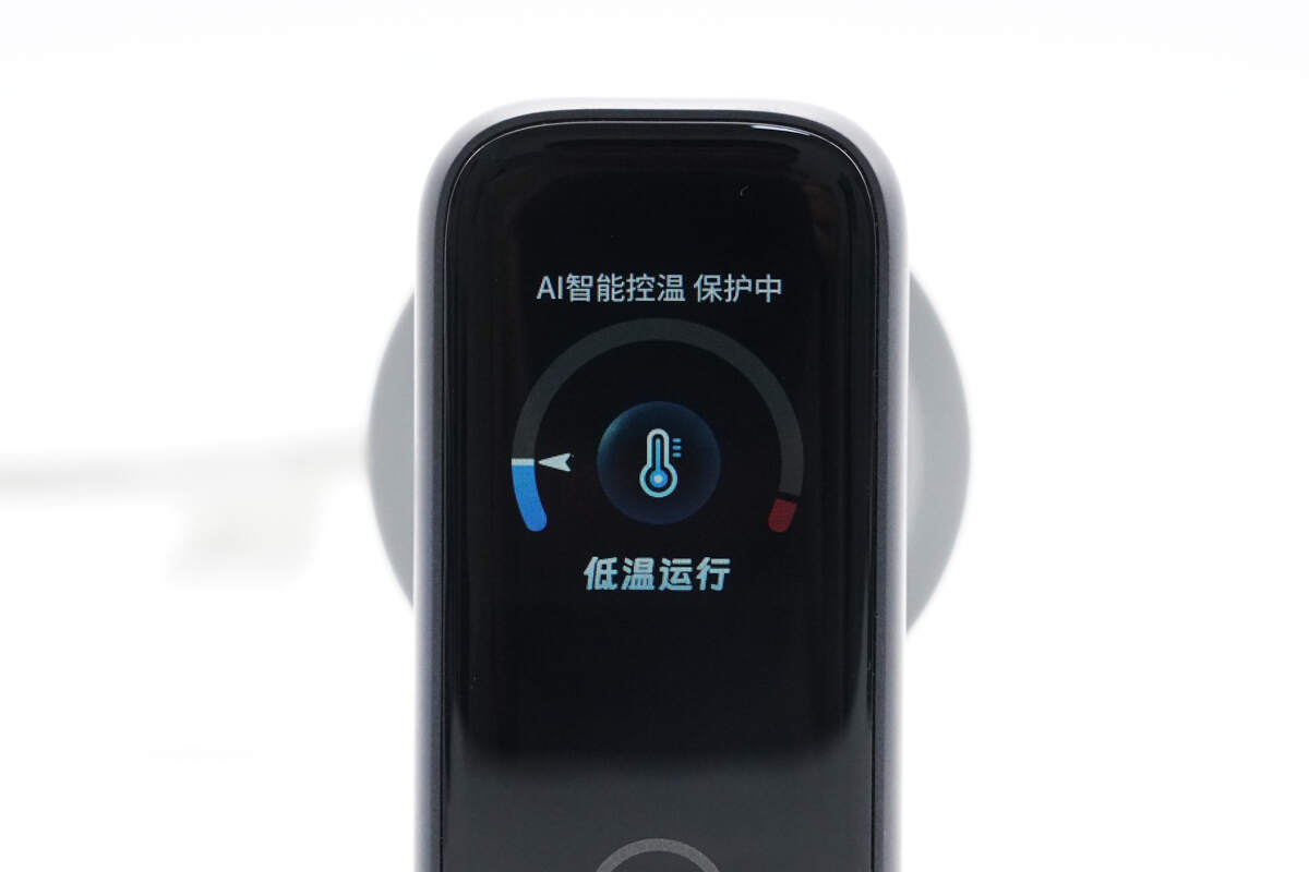
The button allows users to switch the display to view the internal temperature of the charger.
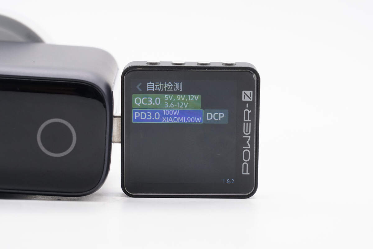
ChargerLAB POWER-Z KM003C shows that the USB-C1/C2 supports QC3.0, PD3.0, DCP, and Xiaomi's 90W proprietary protocols.
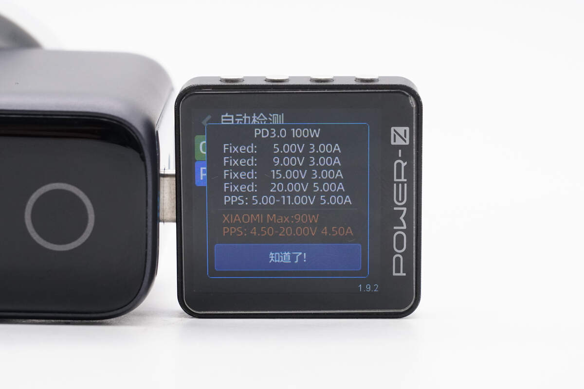
It supports four fixed PDOs of 5V3A, 9V3A, 15V3A, and 20V5A. It also has a set of PPS, which is 5-11V 5A.
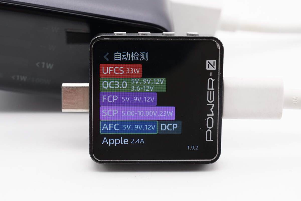
ChargerLAB POWER-Z KM003C shows that the USB-A supports UFCS, QC3.0, FCP, SCP, AFC, DCP, and Apple 2.4A protocols.
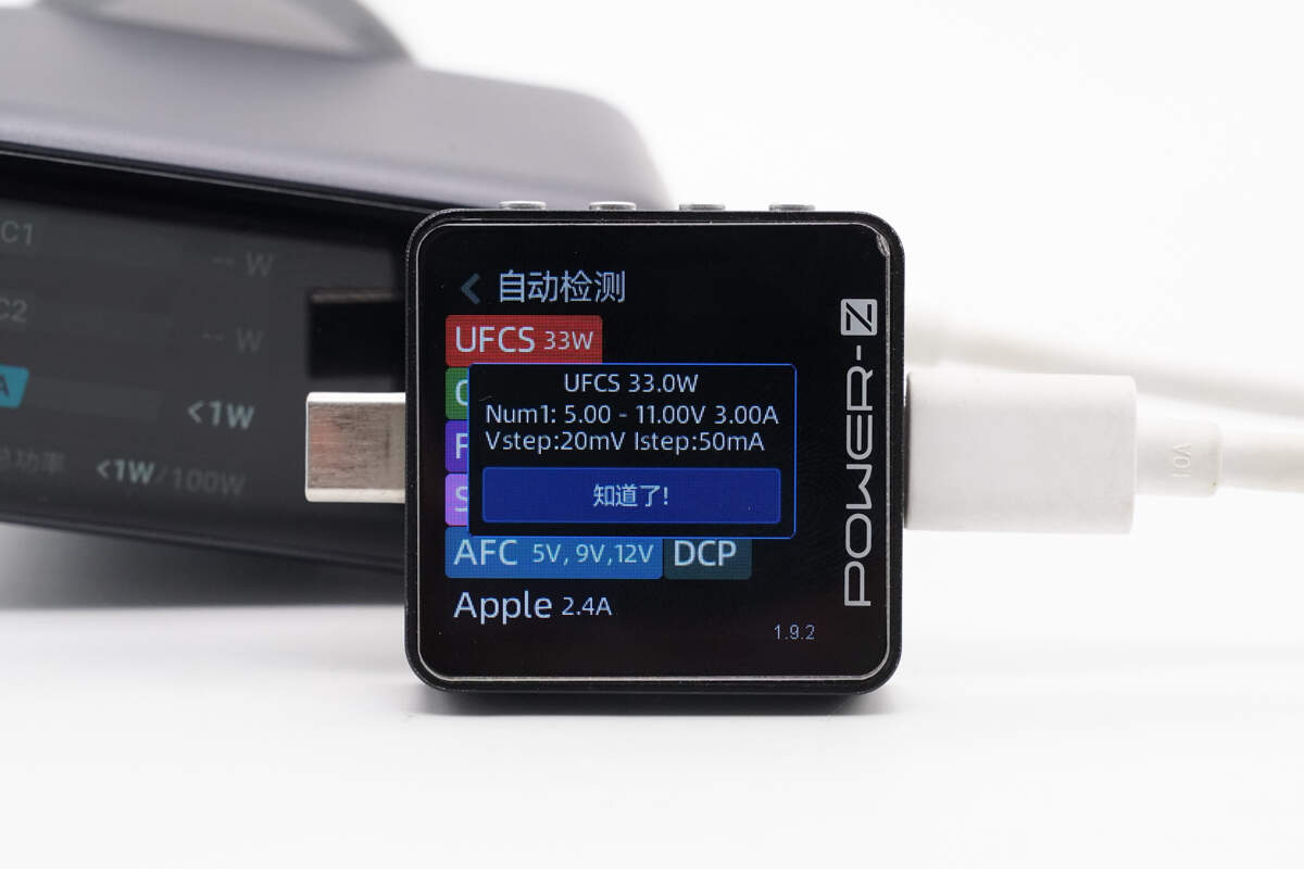
It supports a UFCS voltage range of 5V to 11V at 3A, with voltage adjustable in 20mV steps and current adjustable in 50mA steps.

Using it to charge the Xiaomi 15 Pro successfully activates 90W Max fast charging.
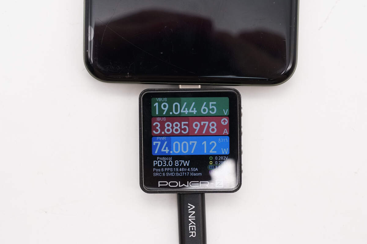
The charging power is about 74W.
Teardown
Next, let's take it apart to see its internal components and structure.
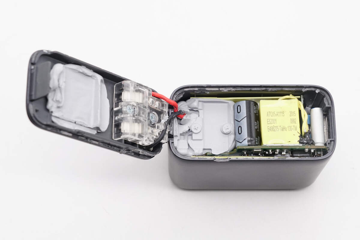
First, pry open the casing along the gap.
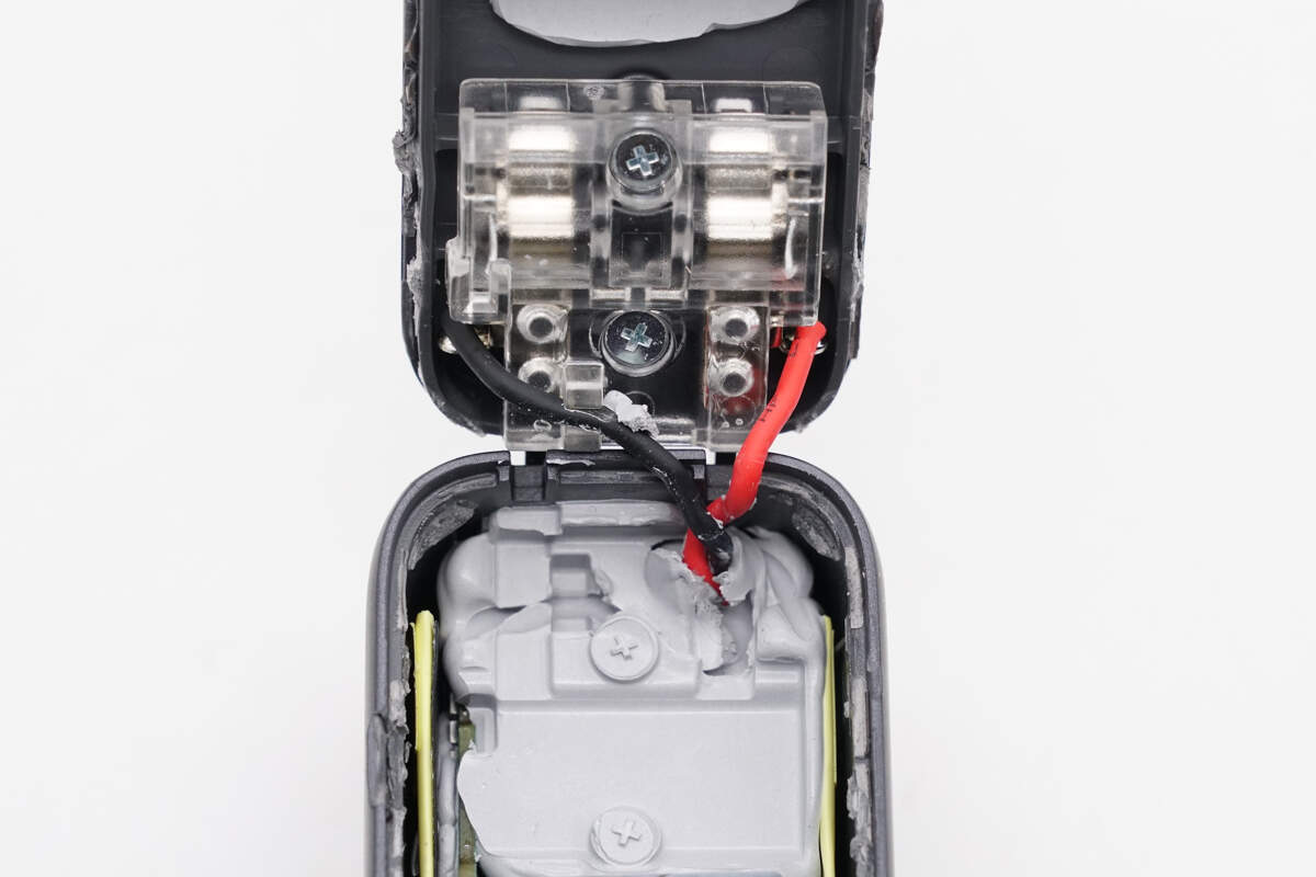
The foldable plug is connected through soldered wires.
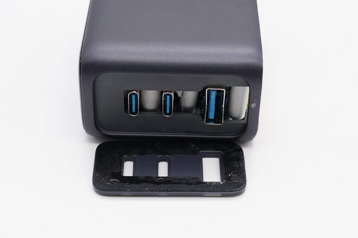
Remove the cover on the output port side.
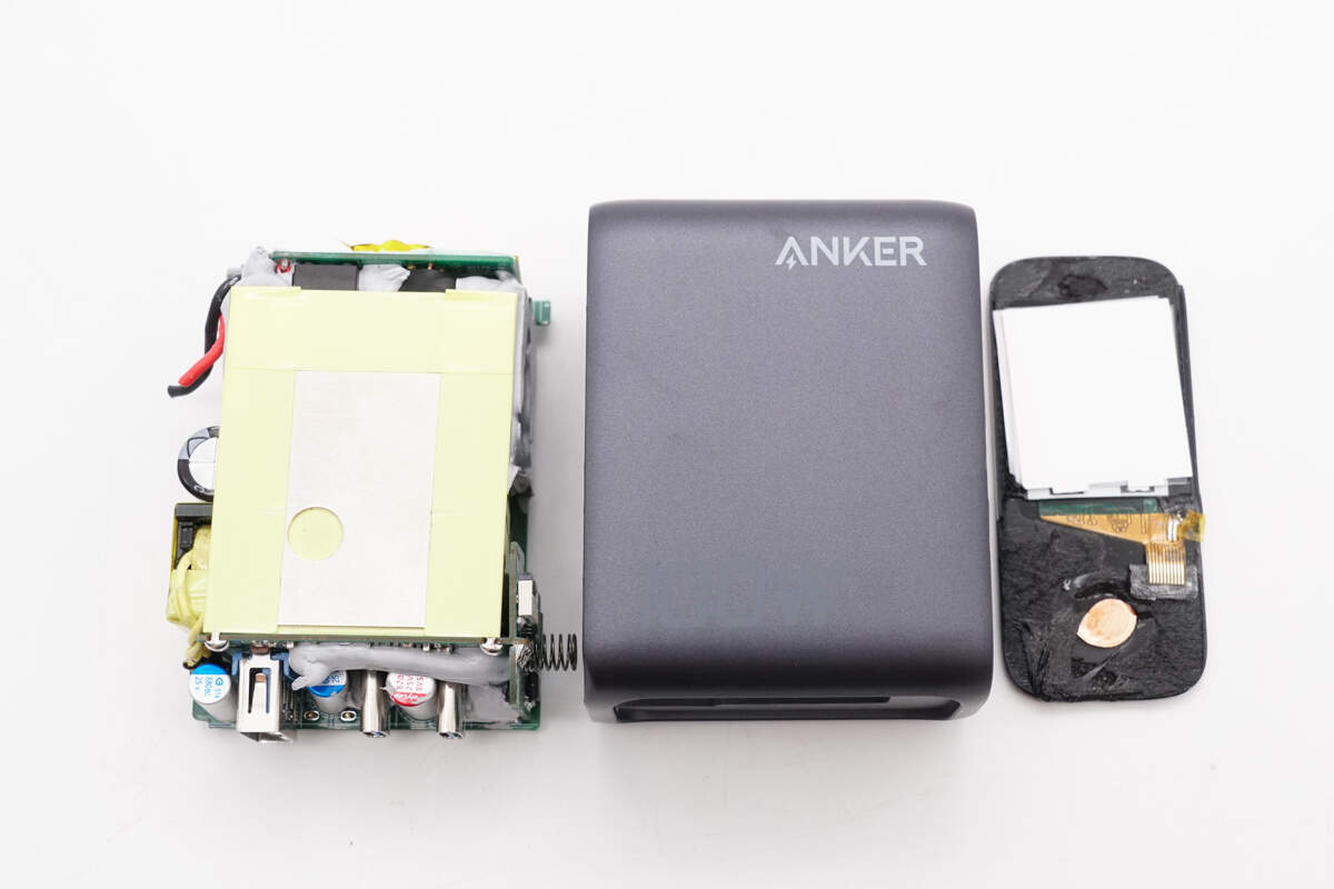
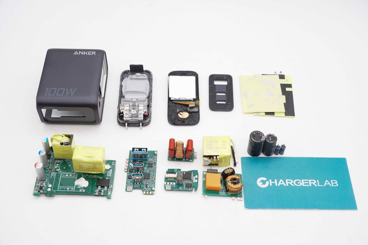
Remove the PCBA module from the casing.
The screen panel is fixed with double-sided tape.
The housing has an opening for the touch spring to pass through and a slot to secure the display.
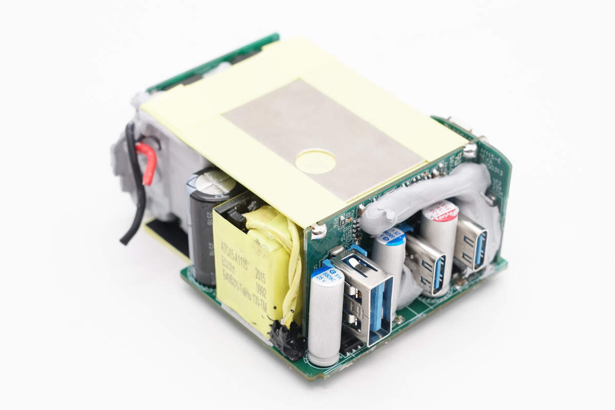
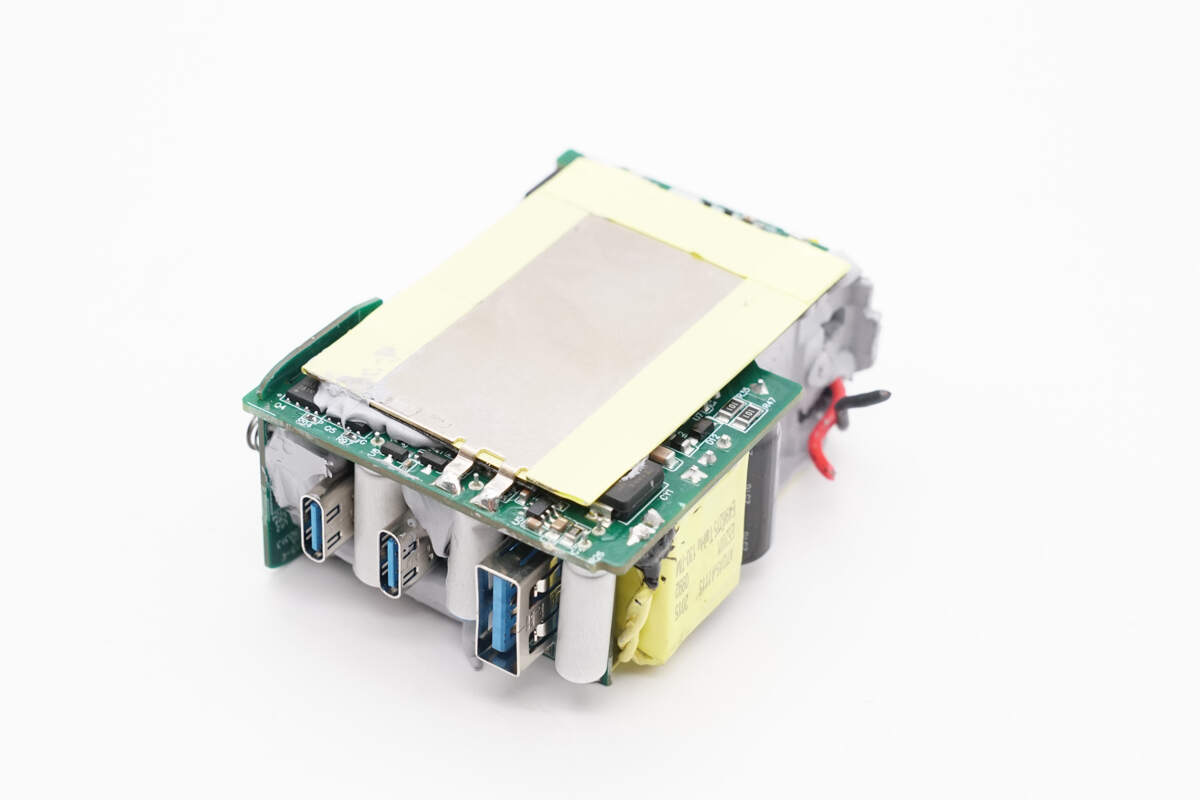
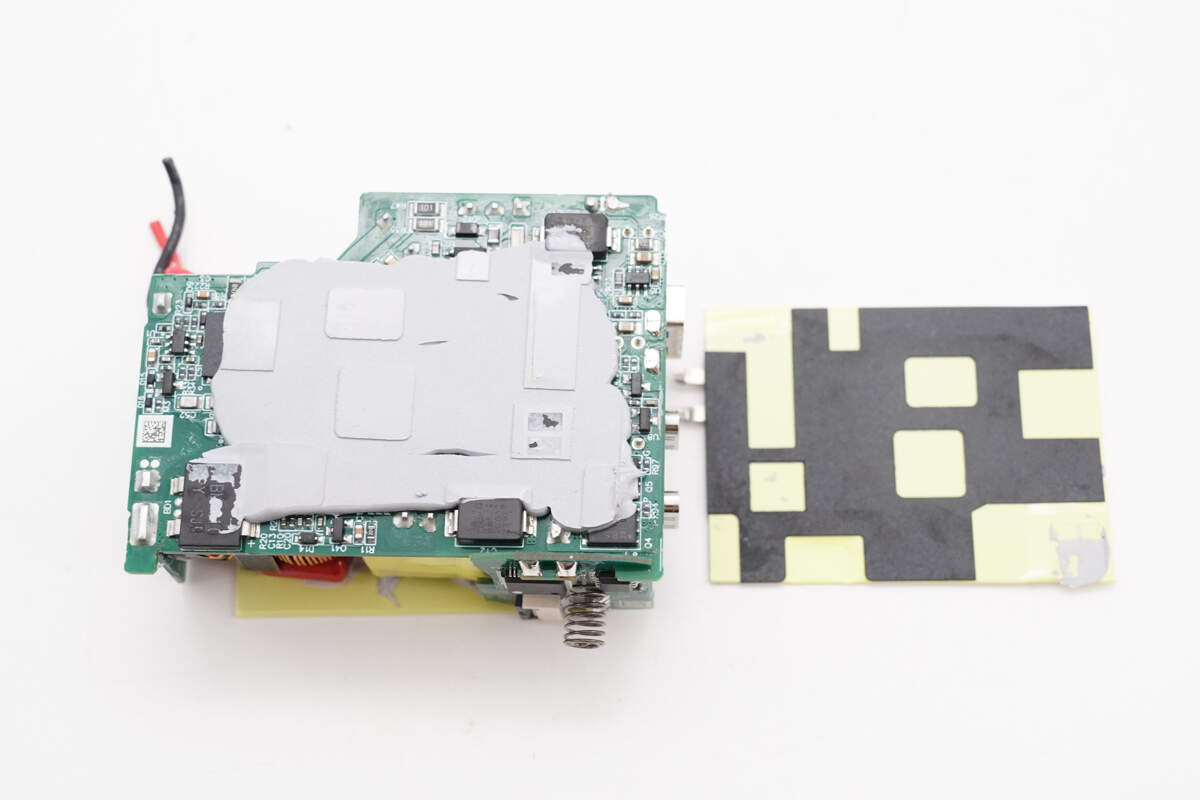
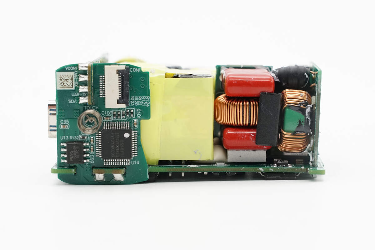
The PCBA consists of several smaller PCBs soldered together, along with multiple heatsinks soldered.
There is a thermal pad attached to this side.
There is a heat sink on the back with tape attached to its edges for insulation.
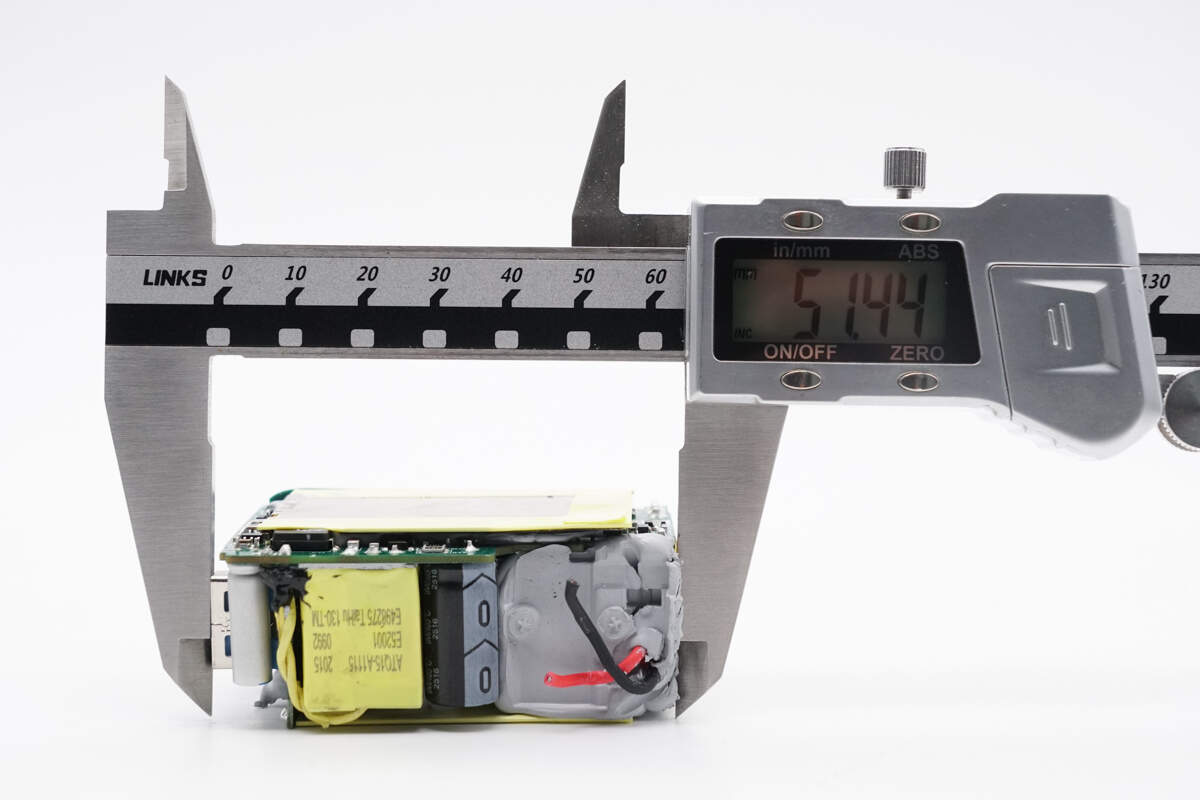
The length of the PCBA module is about 51.4 mm (2.024 inches).
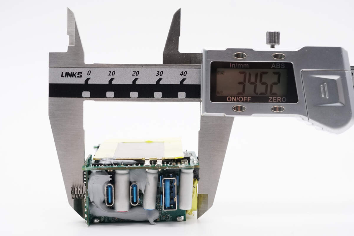
The width is about 34.5 mm (1.36 inches).
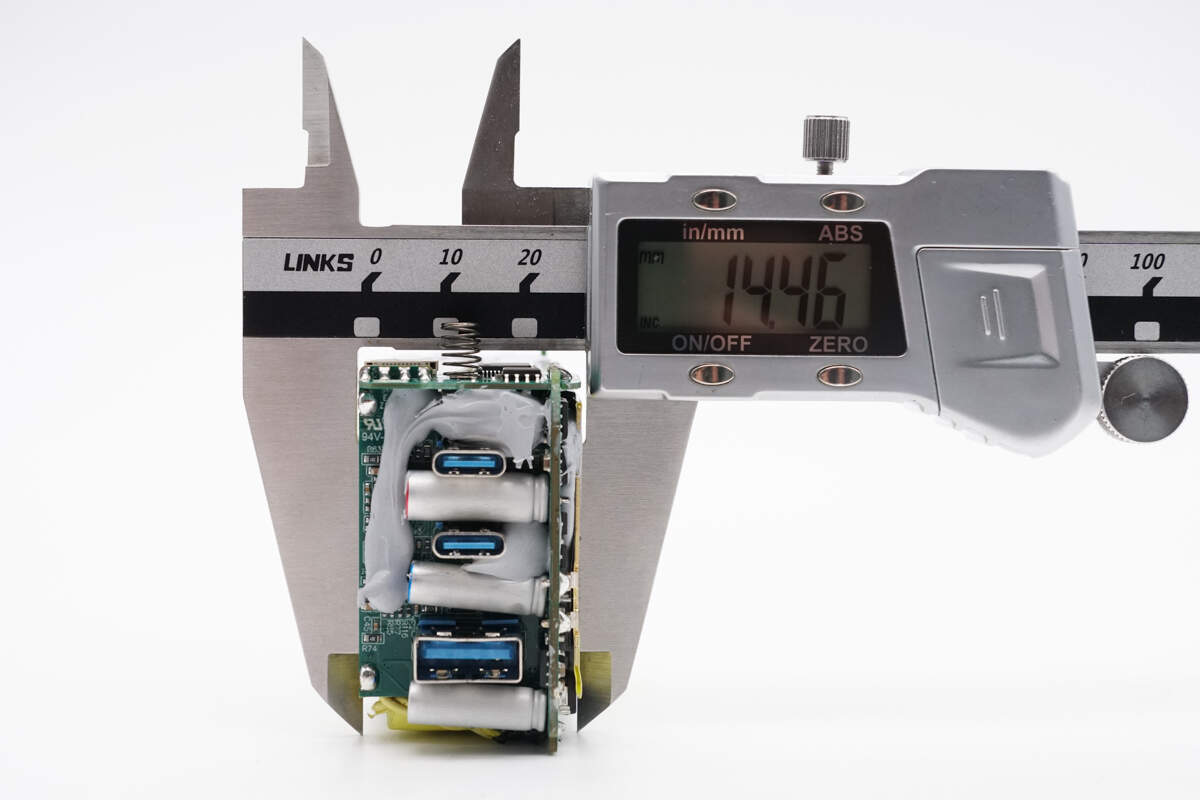
The thickness is about 14.5 mm (0.57 inches).
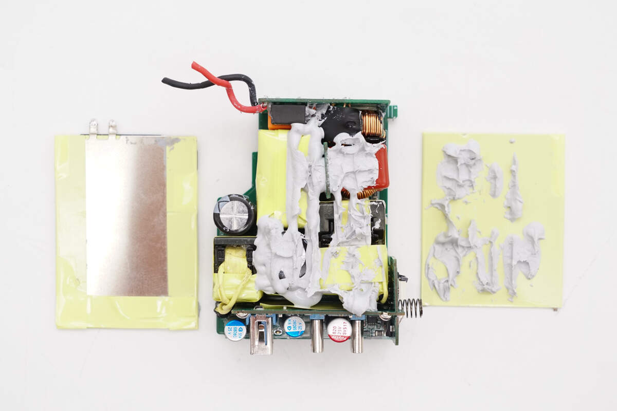
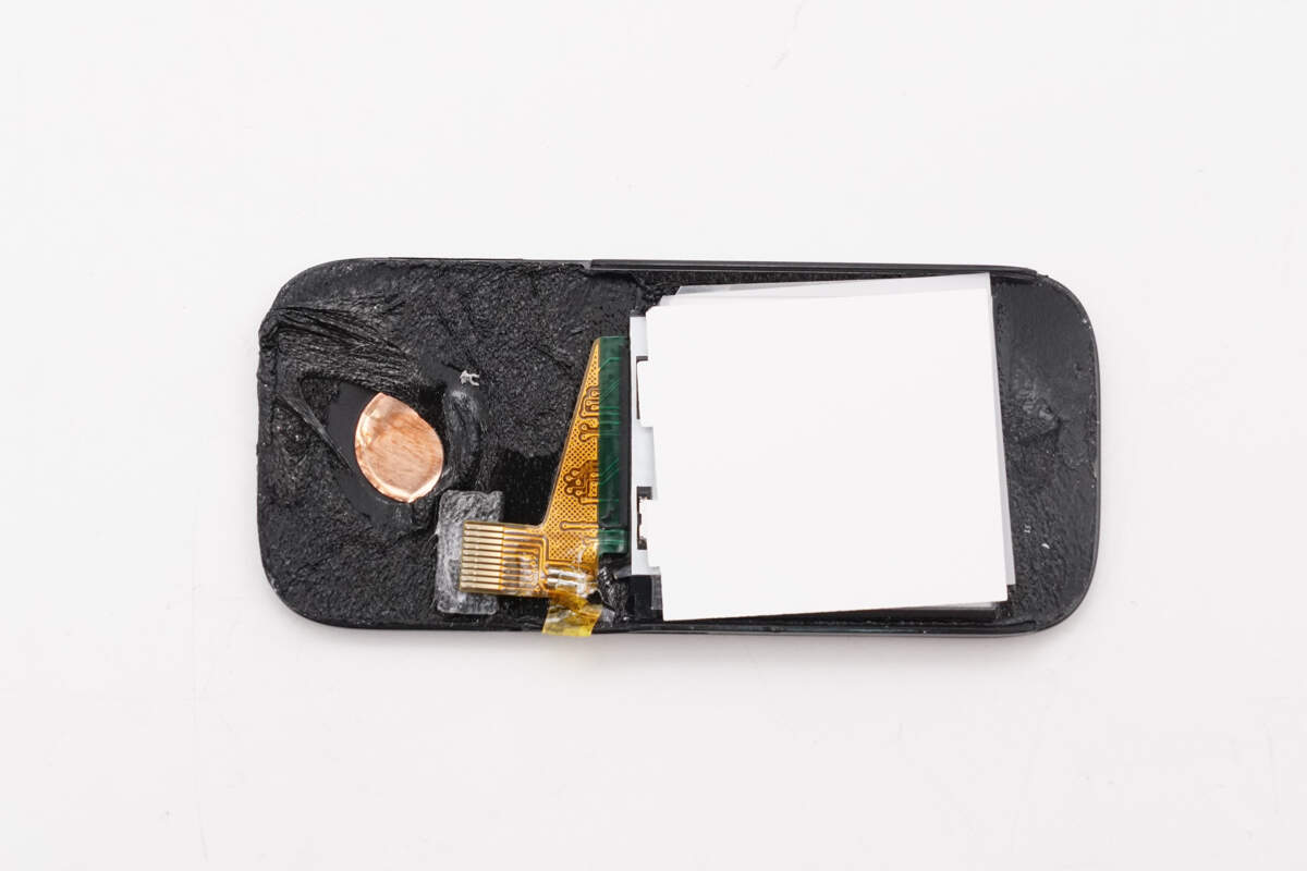
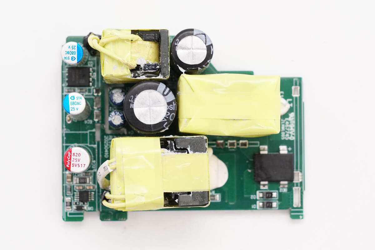
After removing the heatsinks from the surface of the PCBA module, components such as the PFC inductor and transformer can be seen, which are heat-dissipating through the potting compound.
The backside of the PCBA module also uses potting compound for heat dissipation.
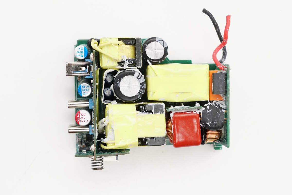
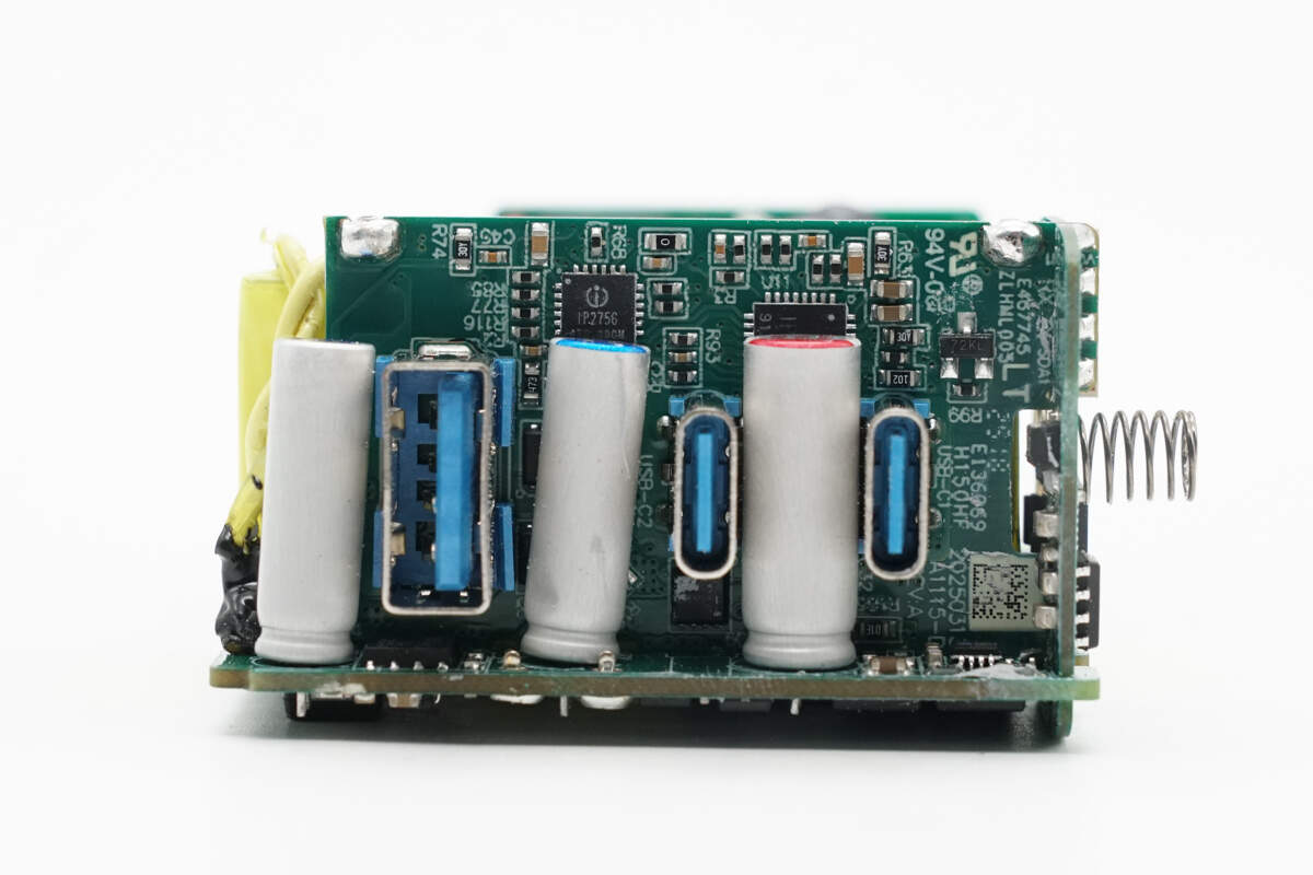
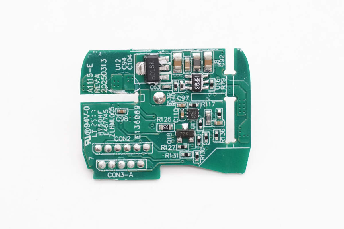
Remove the potting compound. On the front side of the PCBA module, the small PCB on the right handles AC input and includes a fuse, common mode choke, and safety X2 capacitor. At the upper right is the PFC boost inductor, and below it are the filter capacitor and filter inductor. The small output PCB on the left features USB-C and USB-A sockets. To the right is the transformer and filter capacitor, and at the lower left is a small PCB for the display.
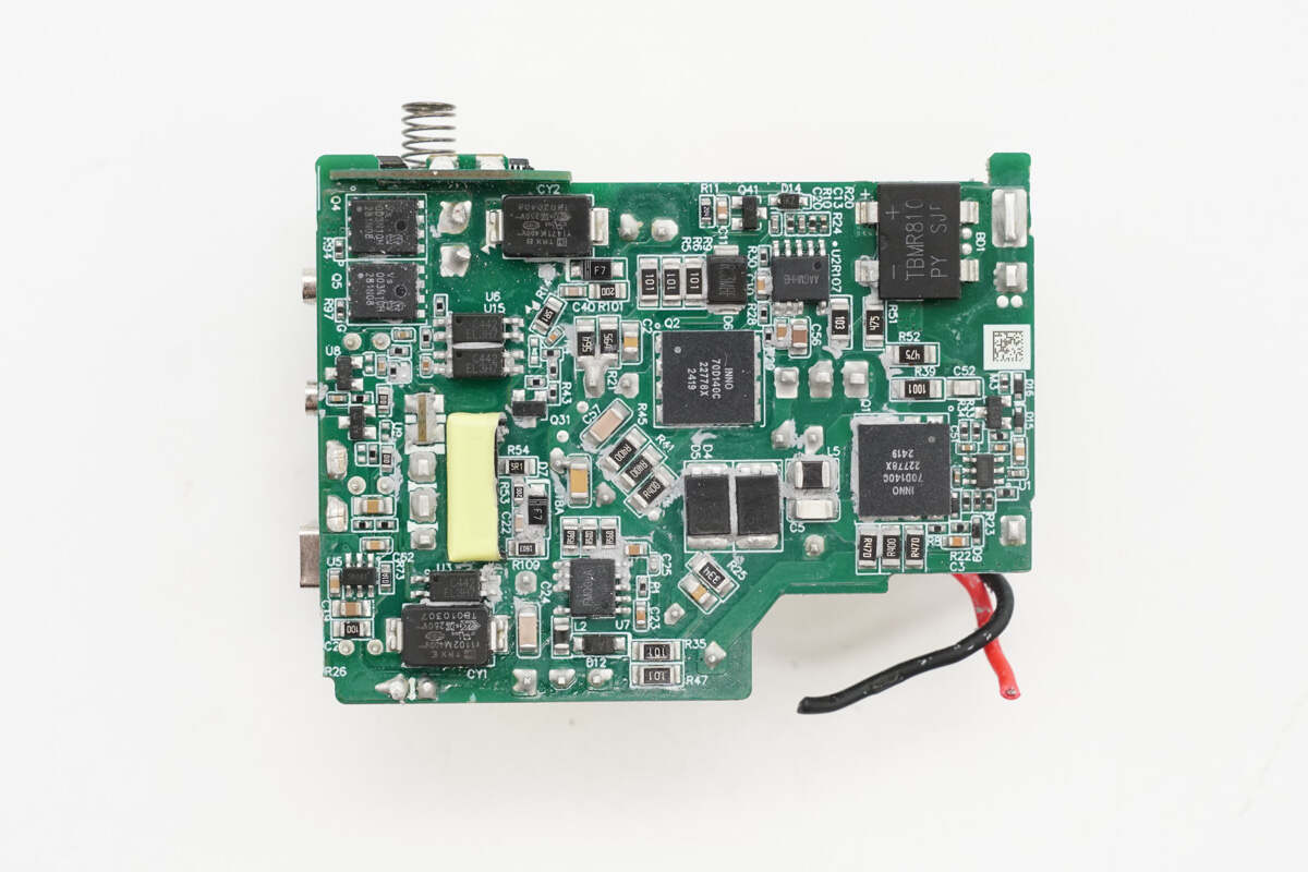
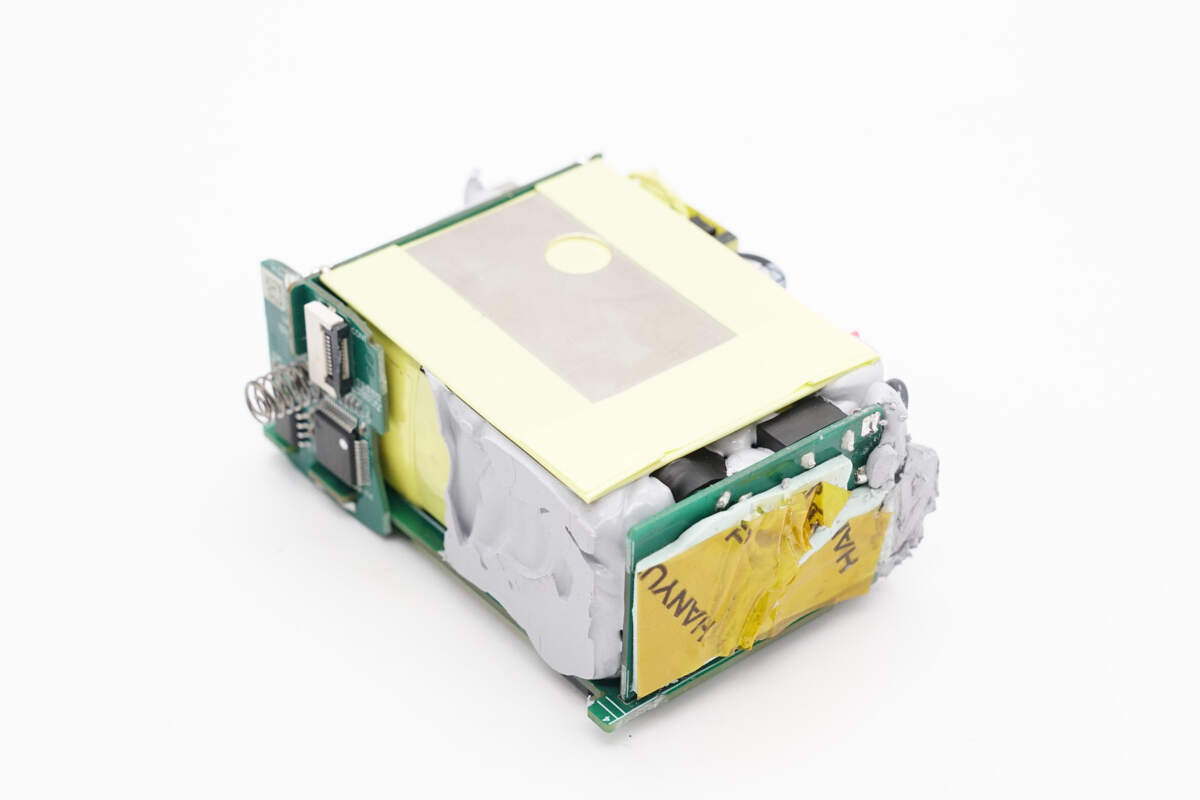
At the upper right corner of the back side is the bridge rectifier, with the PFC controller and GaN FET located below it. In the center are the master control chip and another GaN FET. The upper left corner contains two synchronous rectifiers, while the lower left houses the power management controller chip and a synchronous rectifier controller. Between the primary and secondary sides, there are two SMD Y capacitors and three feedback optocouplers.
This side has a display PCB and a filter PCB.
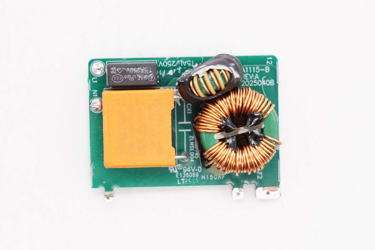
Remove the small side PCB, which contains a fuse, a safety X2 capacitor, and two common mode chokes.
There are SMD resistors on the back.
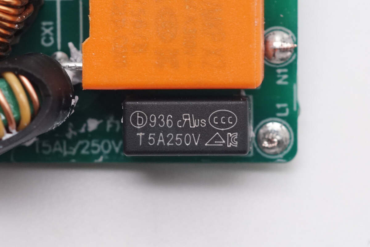
The fuse is from Betterfuse. 5A 250V.
The common mode choke is wound with a magnet and insulated wires, and it's also insulated with bakelite
The safety X2 capacitor is from Surong. 0.47μF.
The common mode choke is wound with magnetic ring, and it's also insulated with bakelite.
The PCBA module has a bridge rectifier located at the lower right corner.
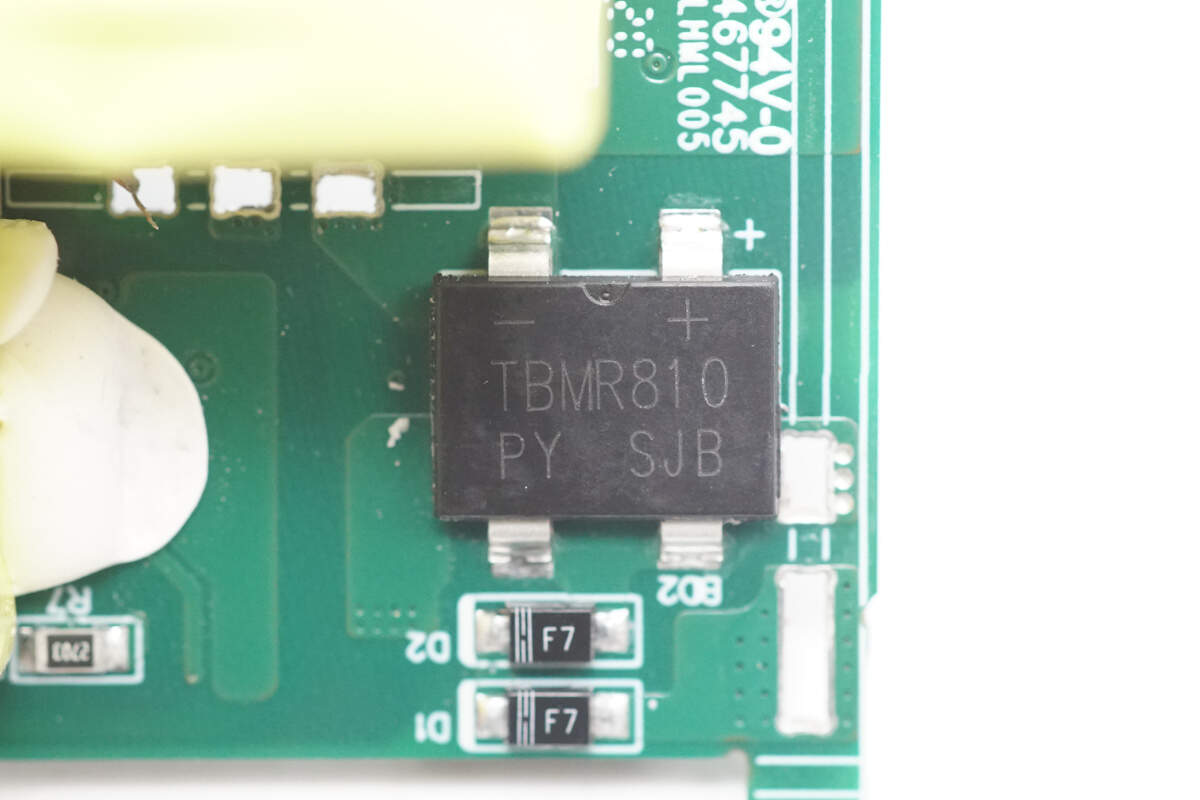
The bridge rectifier is from Pingwei and adopts the TBM package. 8A 1000V. Model is TBMR810.
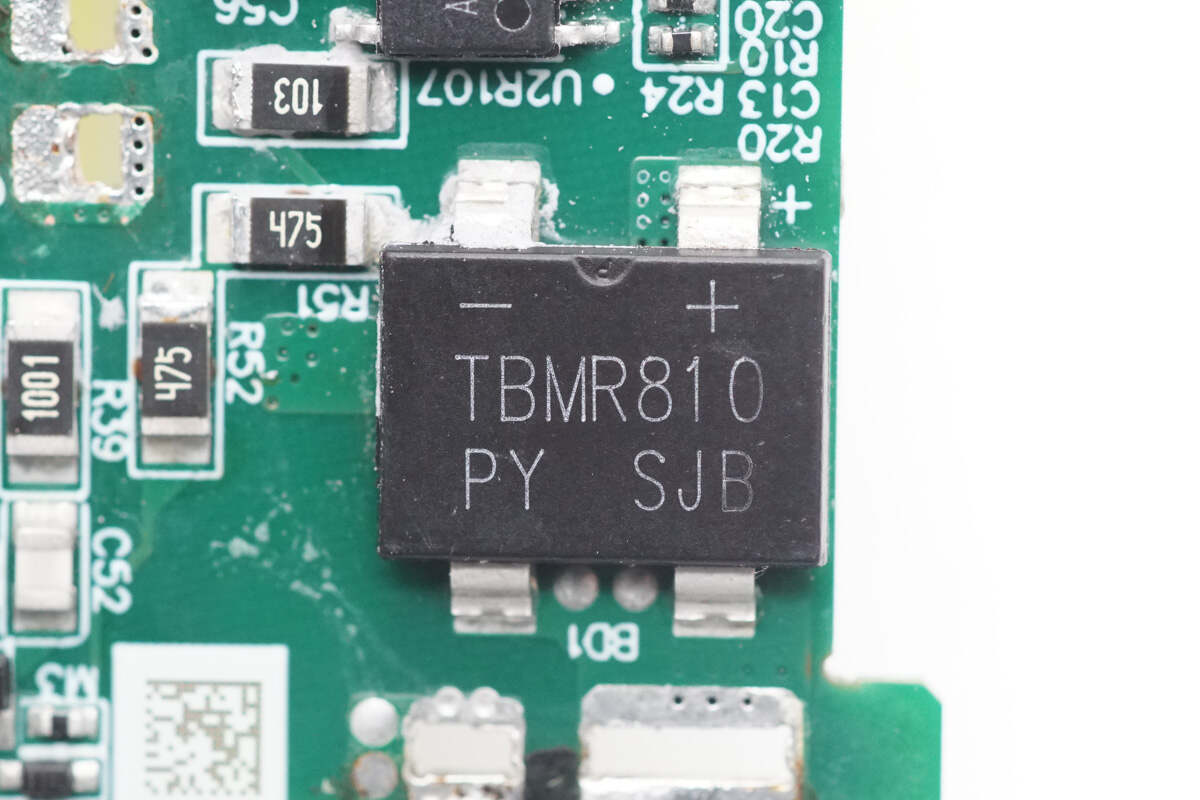
There is another bridge rectifier of the same model on the back side, with both used to share heat dissipation.
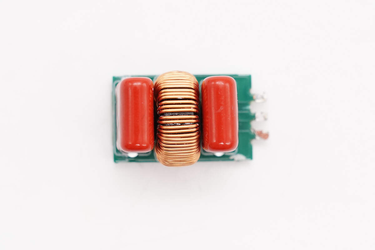
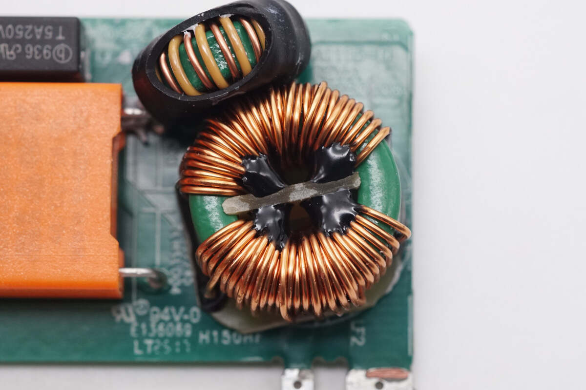
The filter capacitor and filter inductor are soldered on a separate small PCB.
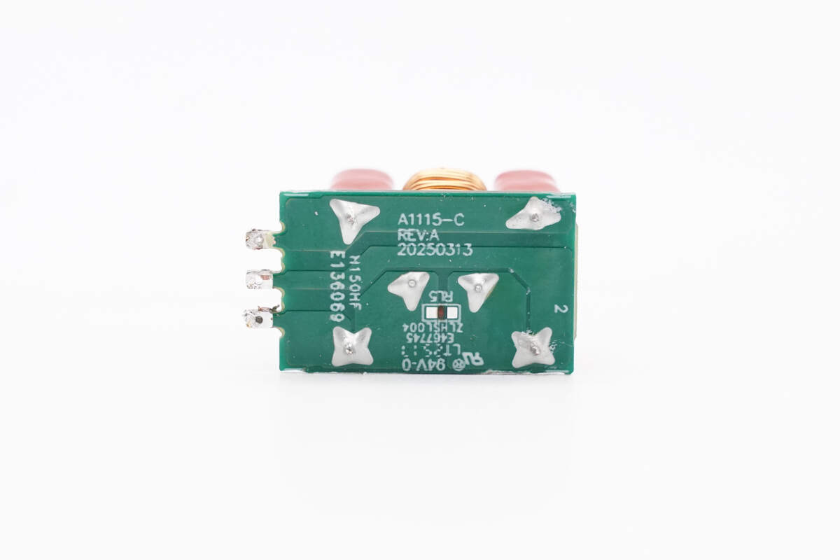
There are no components on the back.
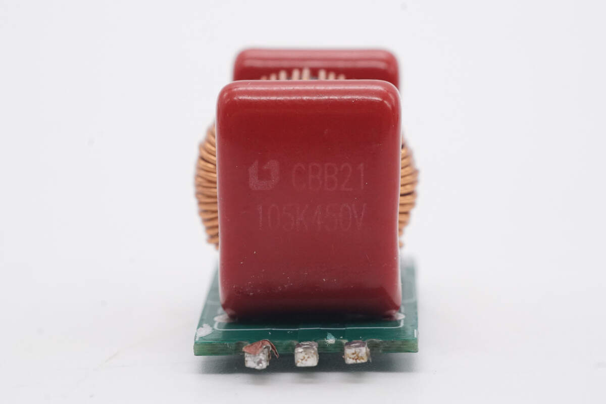
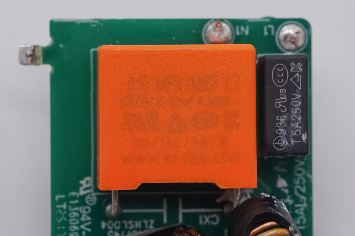
The film capacitor is from the Surong CBB21 series. 1μF 450V.
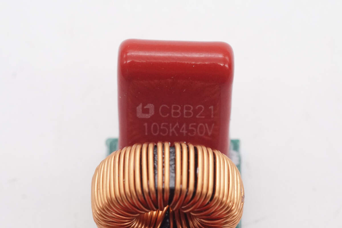
The other film capacitor is the same.
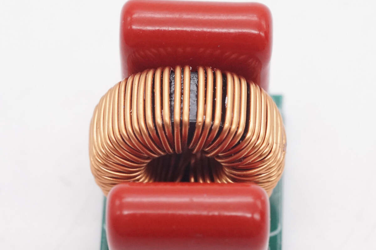
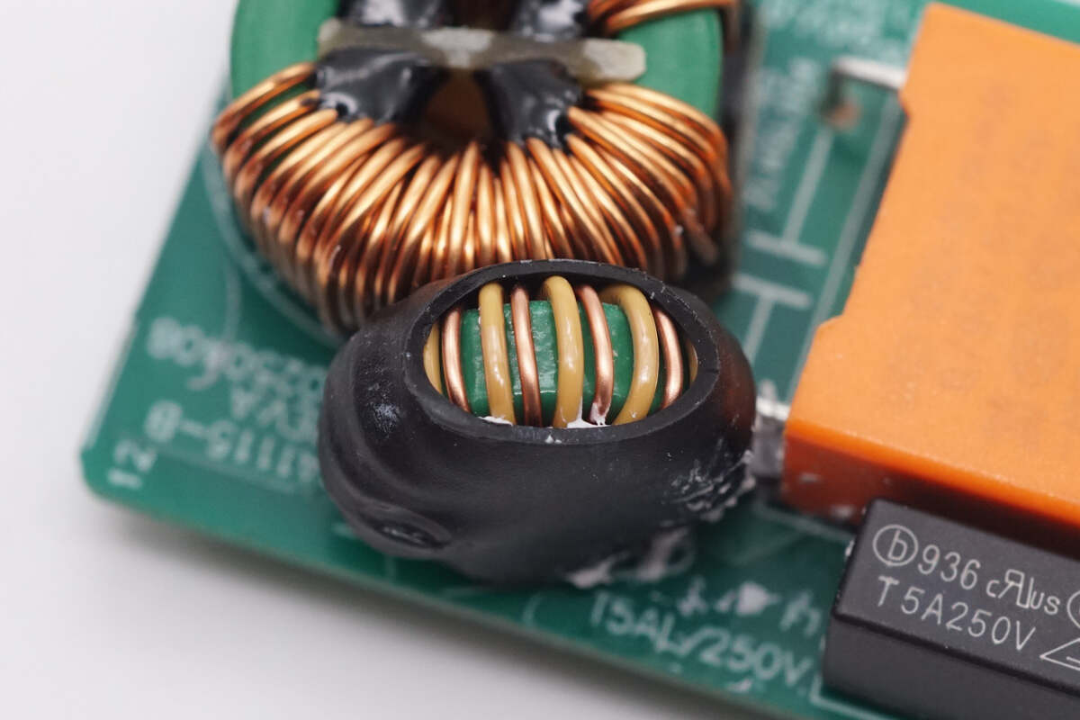
This is a filter inductor wound with magnetic ring.
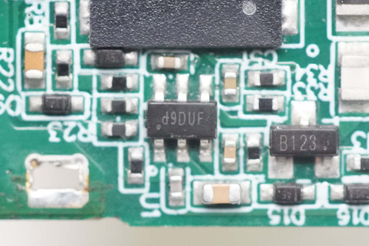
The PFC controller marked with d9 is from Silergy and adopts the SOT23-6 package. It operates in critical conduction mode with a constant on-time control. The built-in boost converter uses quasi-resonant switching with valley switching to achieve high efficiency and optimized EMI performance. Model is SY5072B.
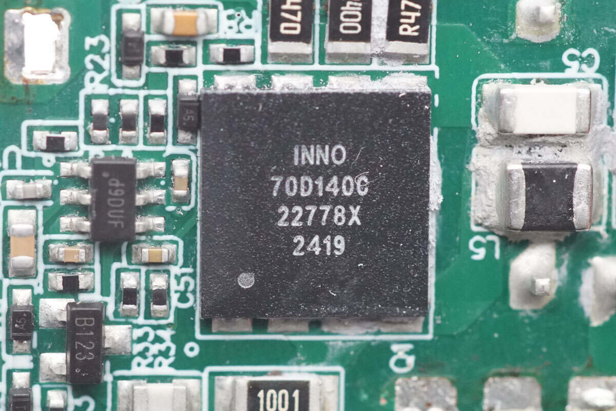
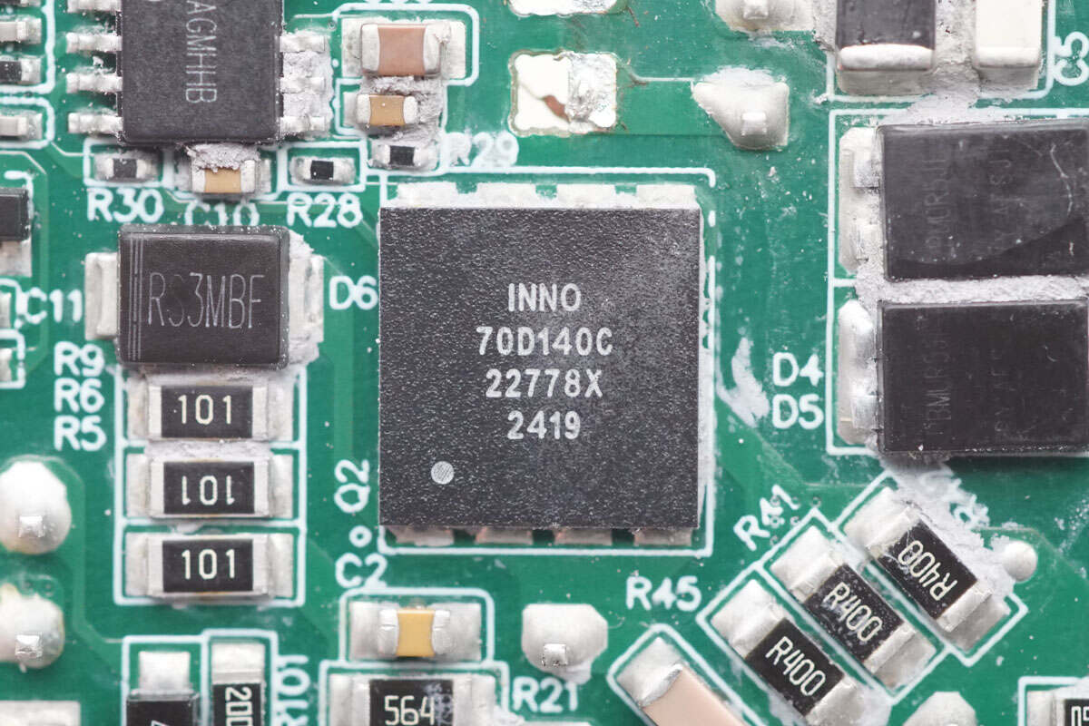
The PFC MOSFET marked with 70D140C is from Innoscience and adopts the DFN8*8 package. It is an enhancement-mode GaN FET with a voltage rating of 700V and a transient voltage rating of 800V, featuring an on-resistance of 140mΩ and a Kelvin source. It has very low gate charge and output charge, meeting JEDEC standards for industrial applications. It includes built-in ESD protection and complies with RoHS, lead-free, and EU REACH regulations. It is suitable for totem-pole PFC, fast charging power supplies, high power density, and high-efficiency switching power supply applications. Model is INN700D140C.
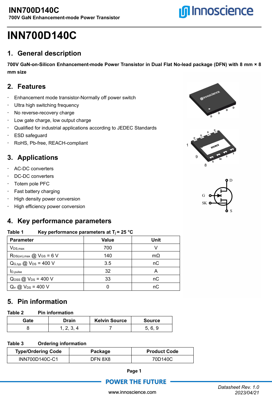
There is information about Innoscience INN700D140C.
The PFC boost inductor is insulated by tape.
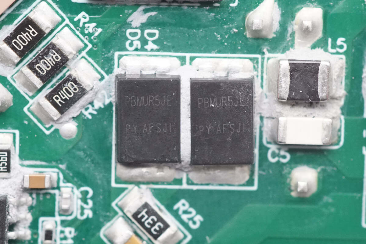
The PFC rectifier is from Pingwei and adopts the PS-277B package. 5A 600V. Model is PBMUR5JE.
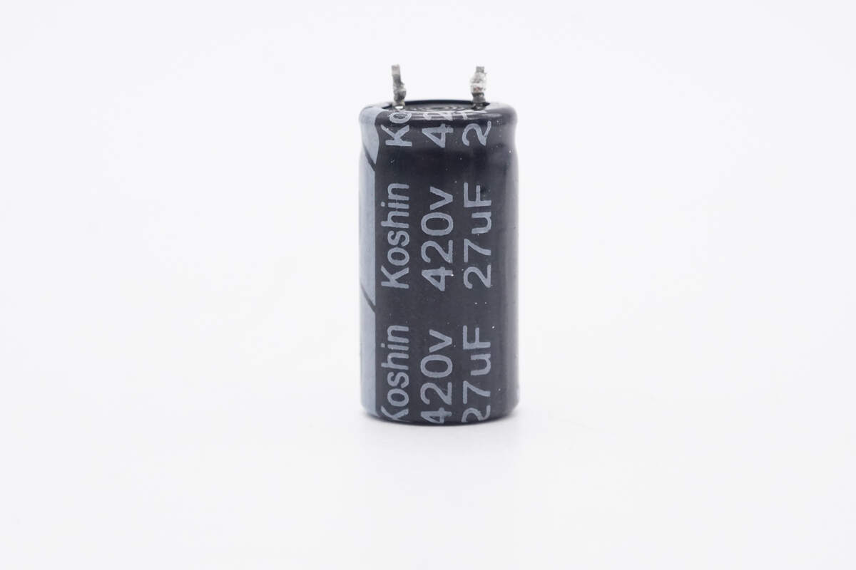
The high-voltage filter capacitor is from Koshin. 420V 27μF.
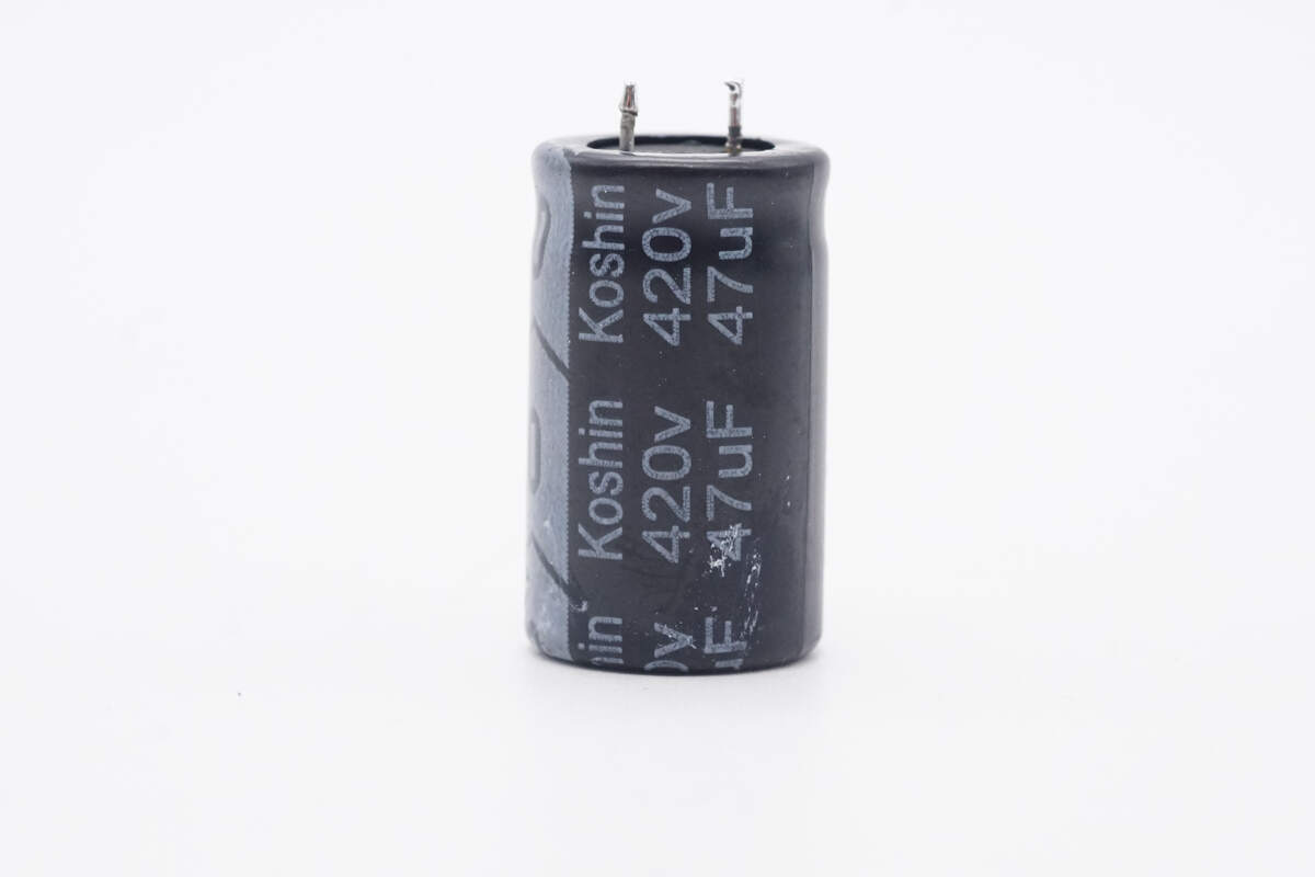
The other capacitor is rated at 420V 47μF.
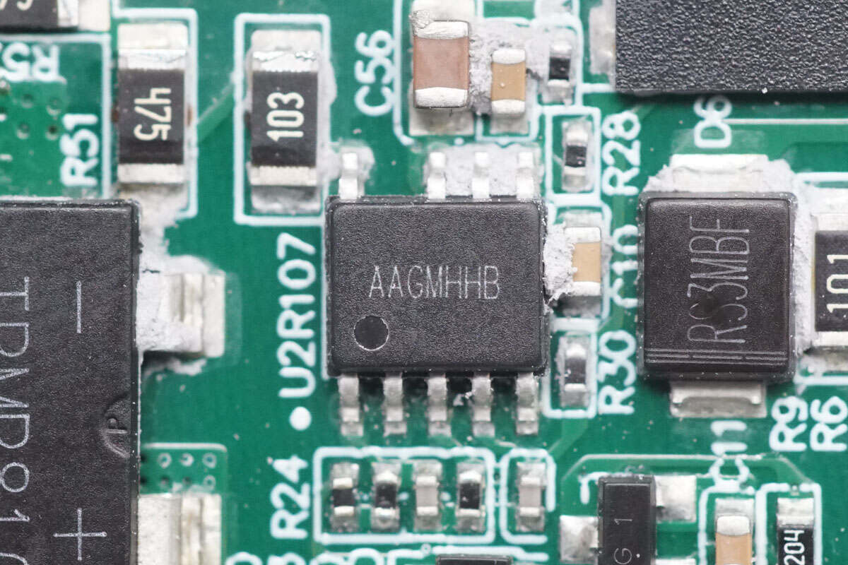
The primary master control chip is from Silergy, marked with AAGM, and adopts the SSOP9 package.
The MOSFET is from Innoscience. Model is INN700D140C.
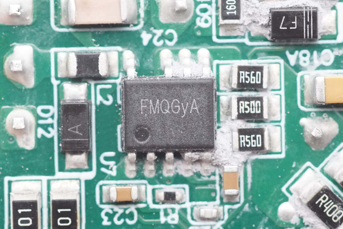
The other primary master control chip is from Silergy, marked with FMQ, and adopts the SSOP9 package.
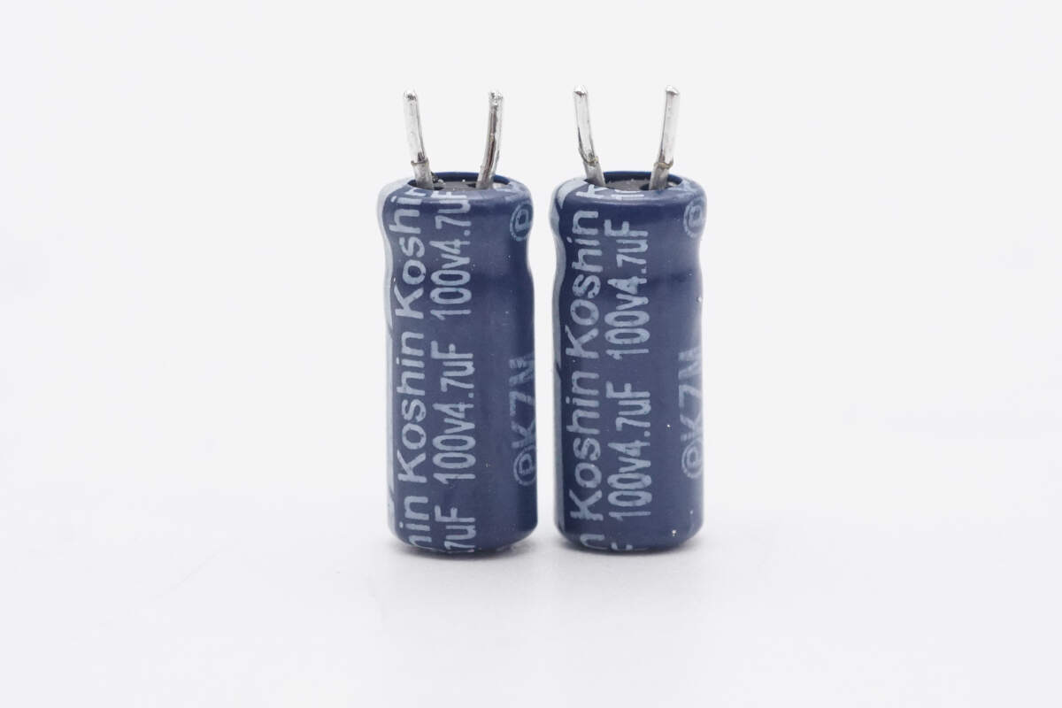
The two filter capacitors that power the primary master control chip are from Koshin. 100V 4.7μF.
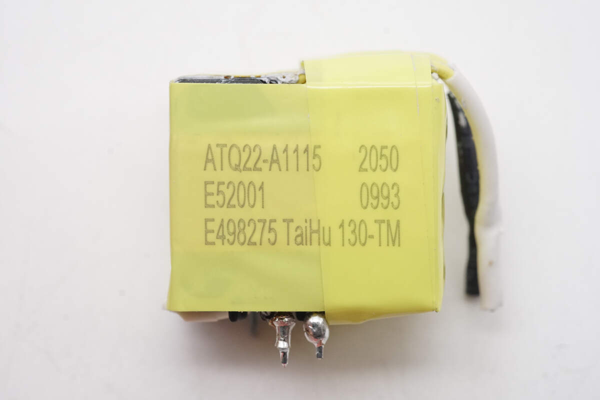
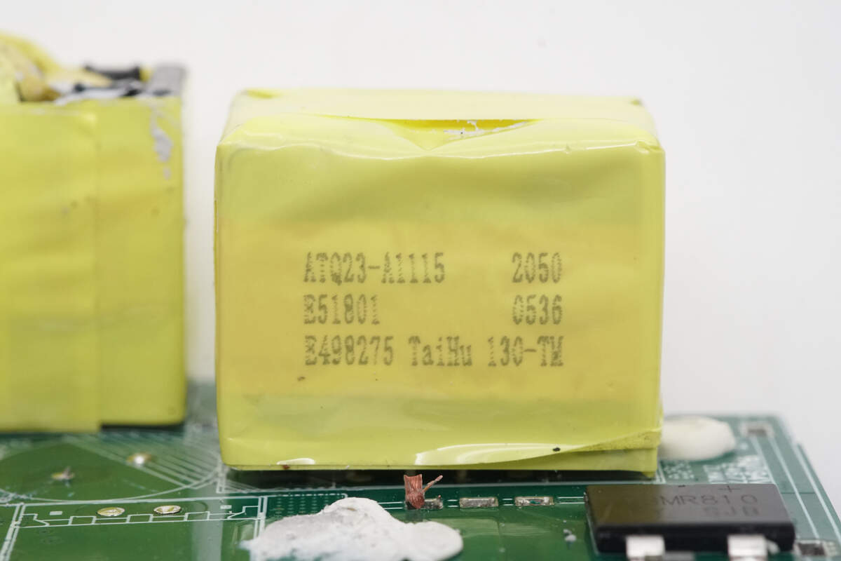
The transformer adopts the ATQ22 magnetic core.
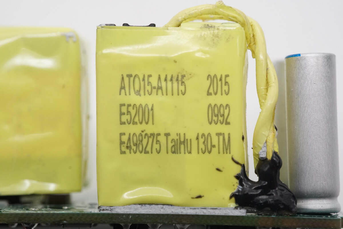
The other transformer adopts the ATQ15 magnetic core.
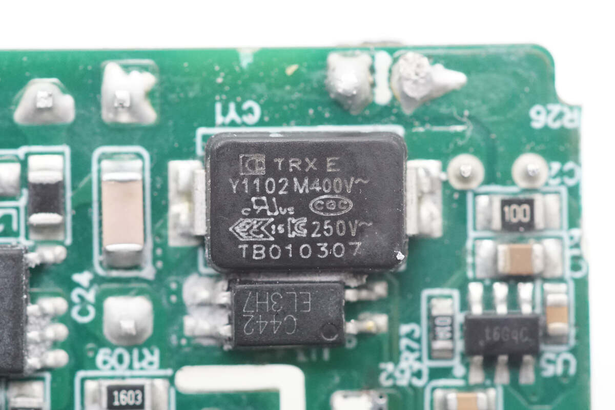
The SMD Y capacitor is from TRX. Its small size and light weight are suitable for high-density power products such as GaN fast chargers.
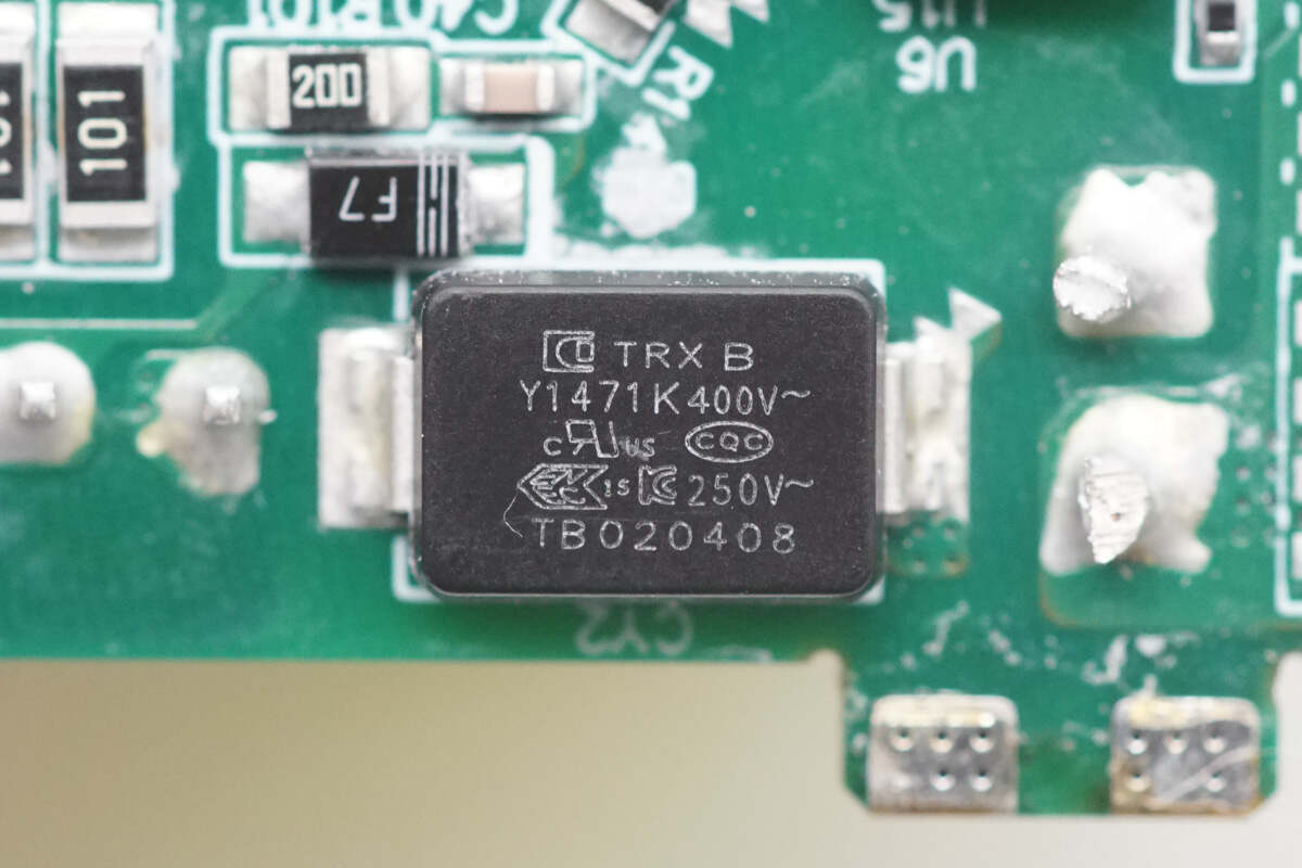
The other SMD Y capacitor is also from TRX.
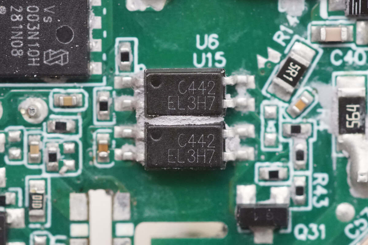
The Everlight EL3H7 optocoupler is used for output voltage feedback.
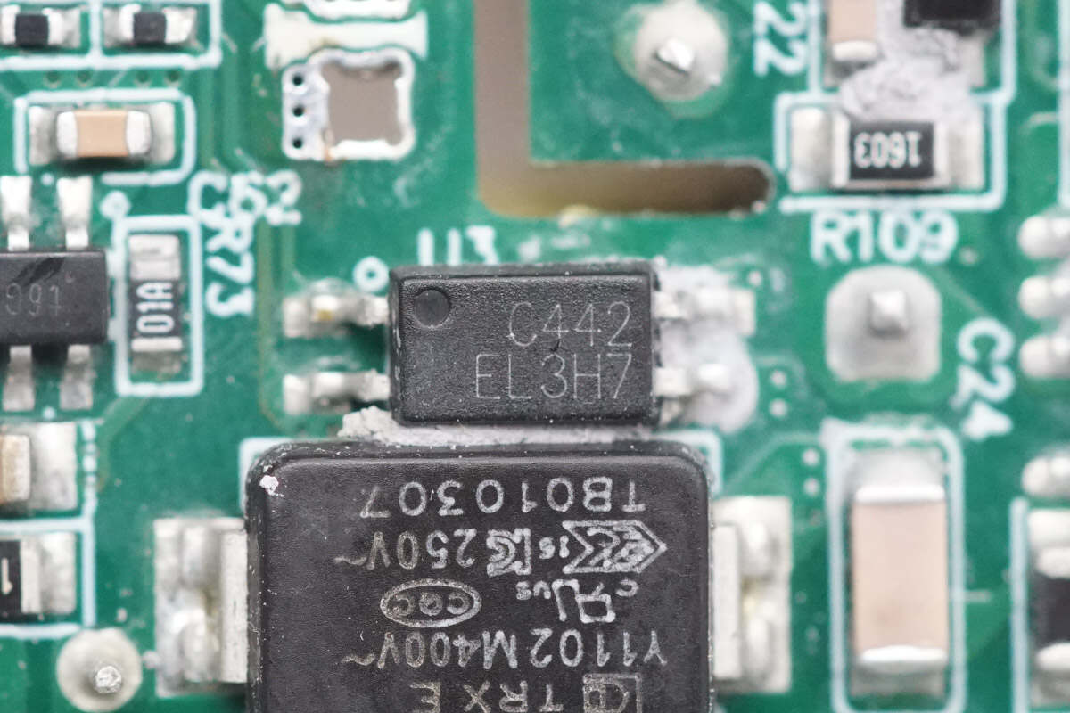
This is another identical optocoupler.
The output side is soldered with a protocol PCB and a solid capacitor.
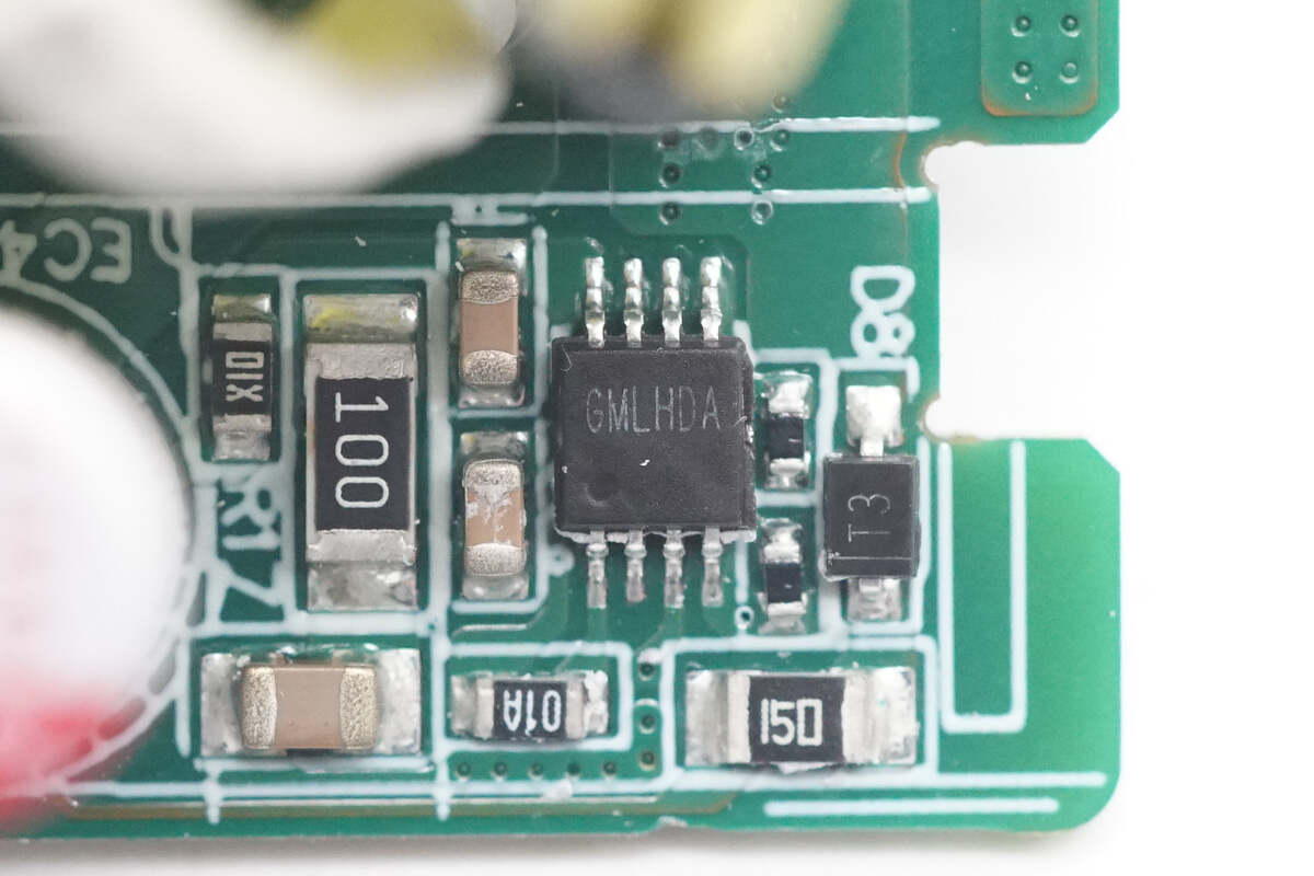
The synchronous rectifier controller marked with GML is from Silergy and adopts the MSOP8 package.
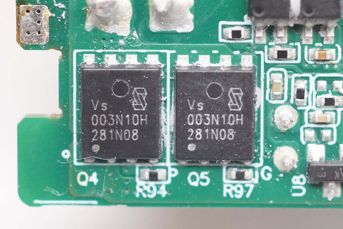
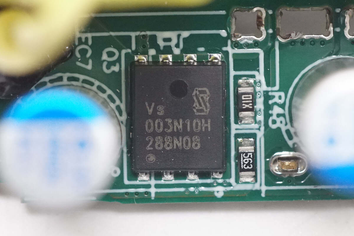
These two synchronous rectifiers are from Vergiga and adopt the PDFN5*6 package. They are connected in parallel. 100V 3.8mΩ. Model is VSP003N10HS-G.
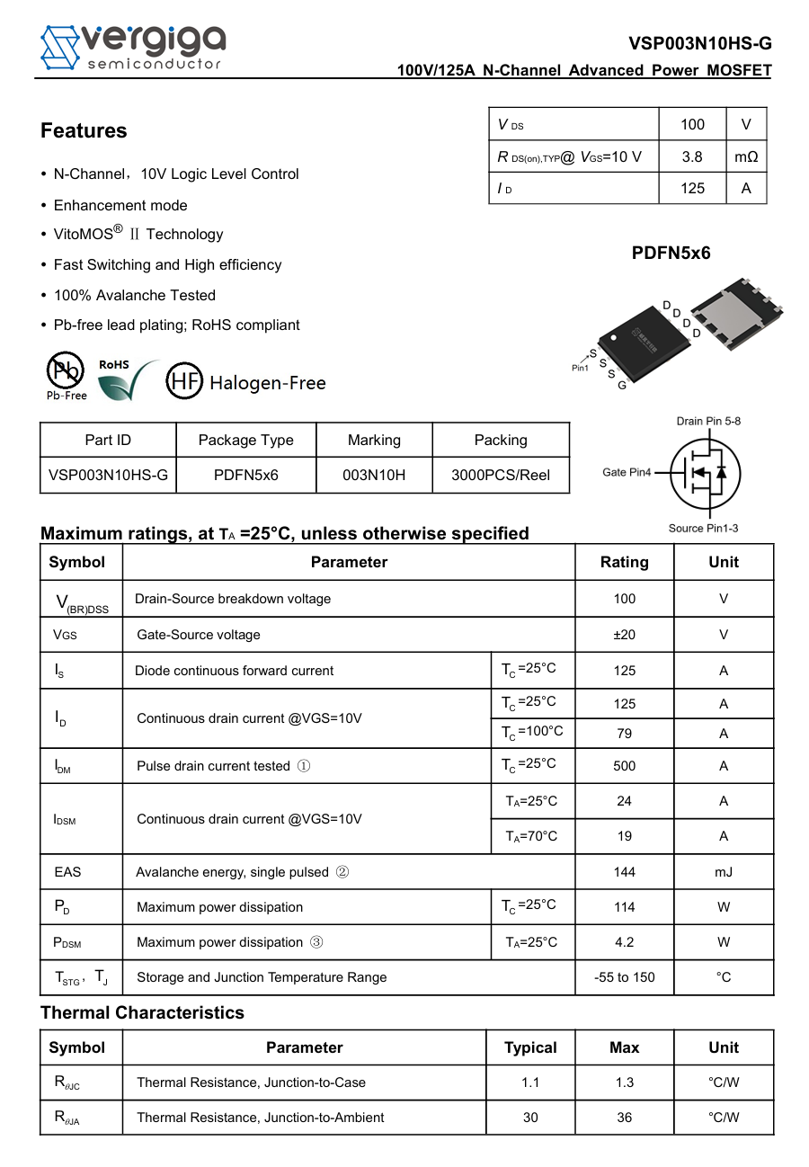
Here is the information about Vergiga VSP003N10HS-G.
The solid capacitor is from BERYL and belongs to the BC series. 80μF 25V.
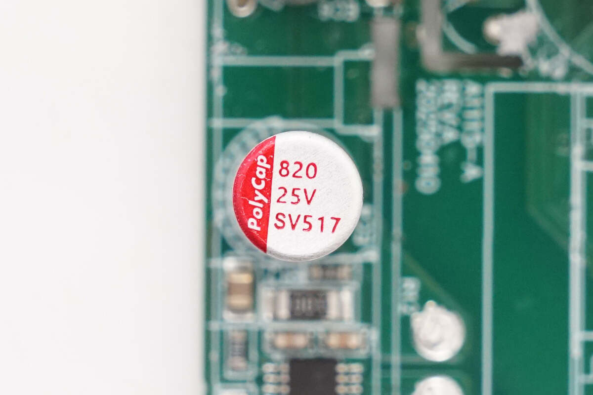
The other capacitor is from PolyCap. 820μF 25V.
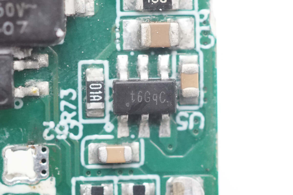
The synchronous rectifier controller marked with t6 is from Silergy and adopts the SOT23-6 package.
The synchronous rectifier is from Vergiga. Model is VSP003N10HS-G.
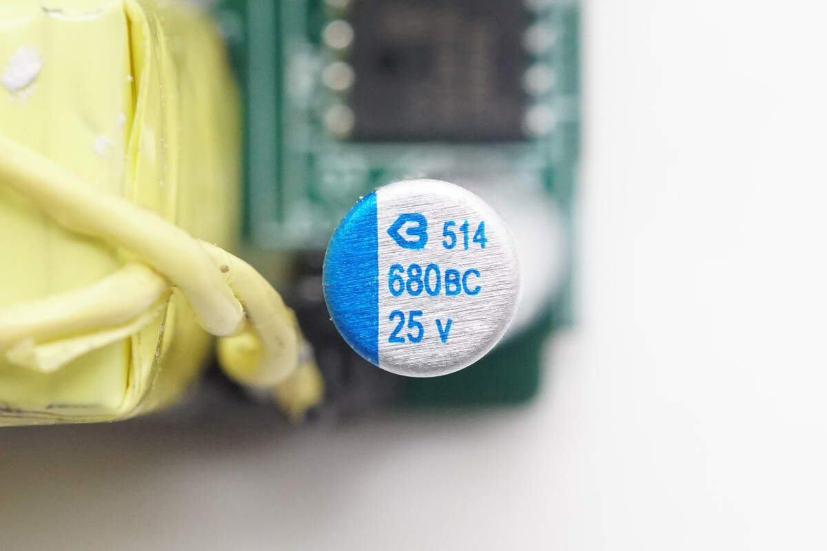
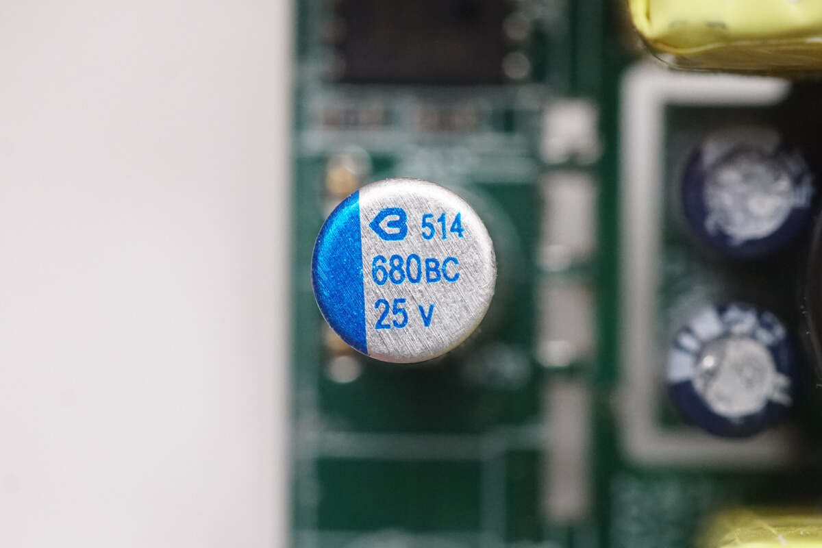
This is the solid capacitor for output filtering. 680μF 25V.
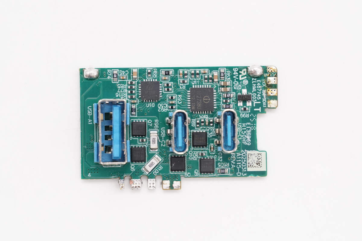
The output protocol PCB features a protocol chip, a VBUS MOSFET, and a current-sense resistor. The USB-C and USB-A sockets are secured through-hole soldering.
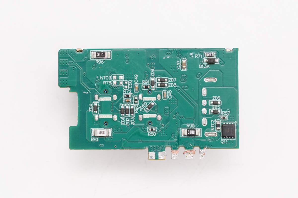
The back is also equipped with a current-sense resistor and a VBUS MOSFET.
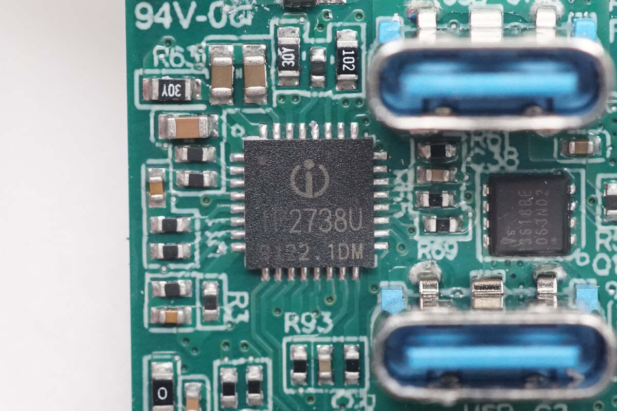
The protocol chips for the two USB-C ports are from Injoinic. They support multiple USB interfaces and are designed for dual-port fast charging applications ranging from 18W to 140W. Each chip features independent feedback control and independent USB PD control, effectively integrating the functionality of two IP2736 chips into one. The fast charging specifications are identical to those of the IP2736. They support USB PD3.1 with the 28V EPR mode, UFCS (Universal Fast Charging Specification), as well as a comprehensive range of fast charging protocols, including PD3.0 and PPS, offering excellent compatibility. Model is IP2738U.
It integrates four independent NMOS drivers, which can be used for controlling multiple output ports, switching between multiple VBUS MOSFETs, and managing dual power rail parallel output. It also supports dual-channel independent overcurrent, overvoltage, and short-circuit protection to ensure safe operation.
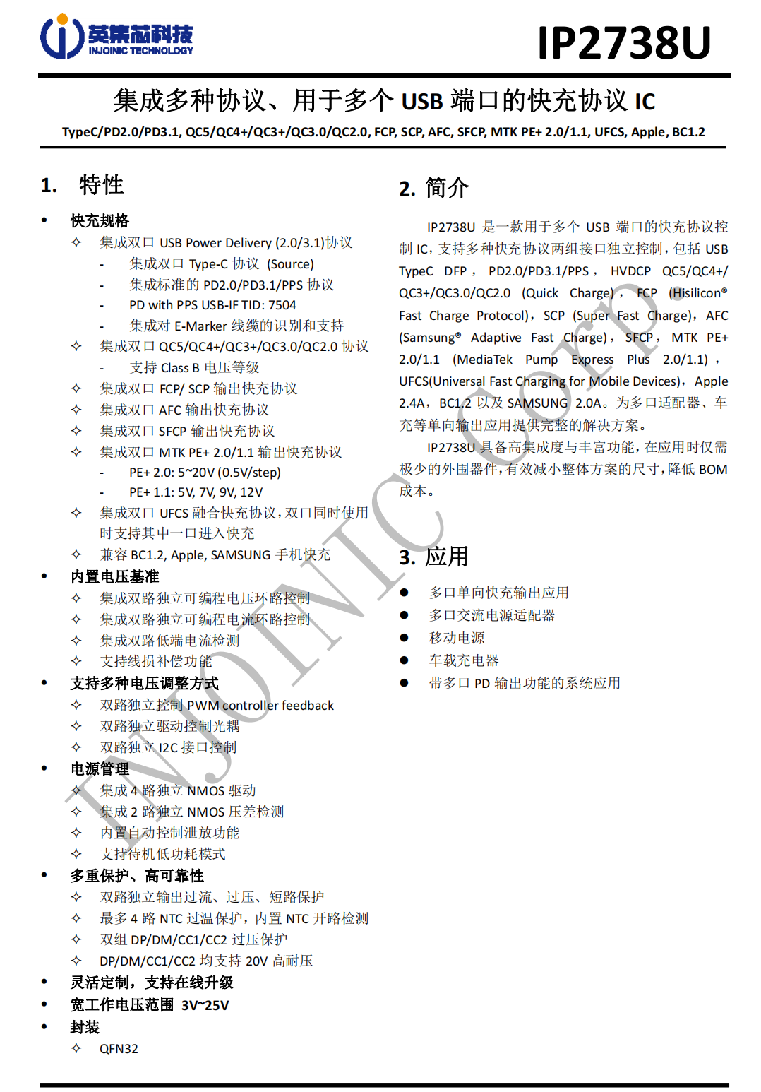
Here is the information about Injoinic IP2738U.
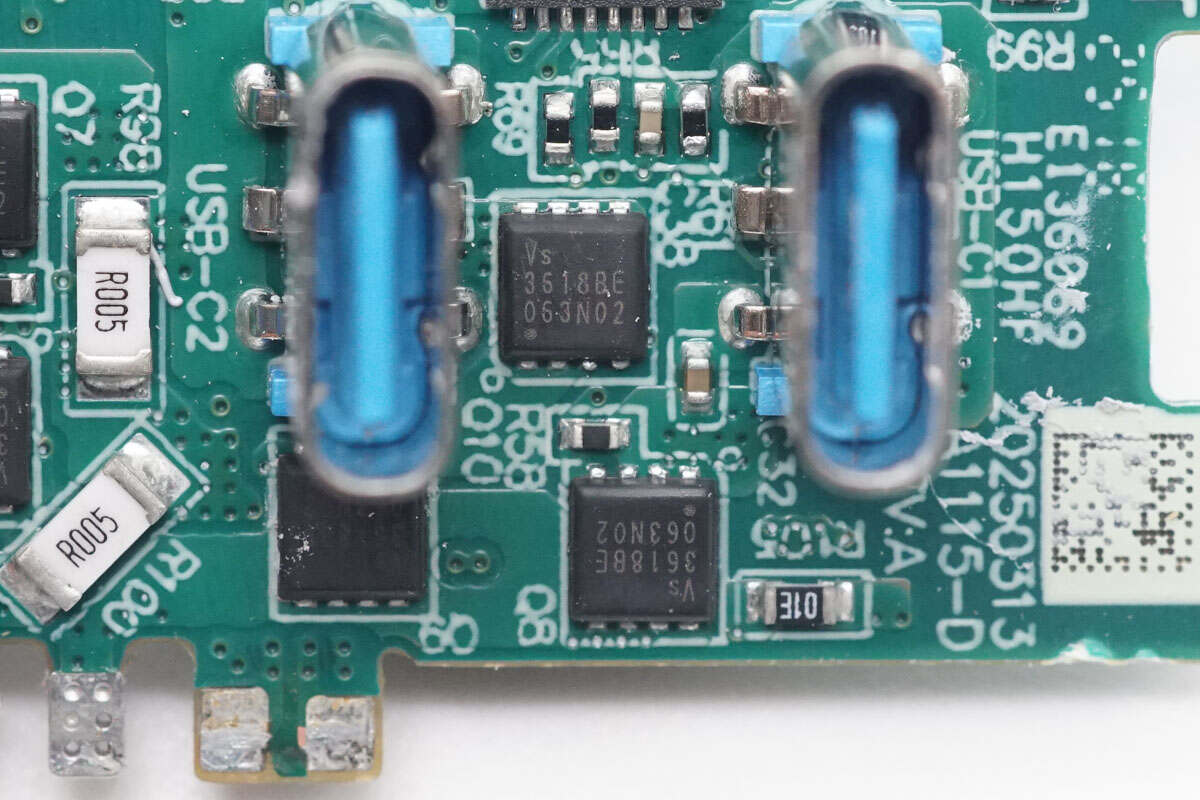
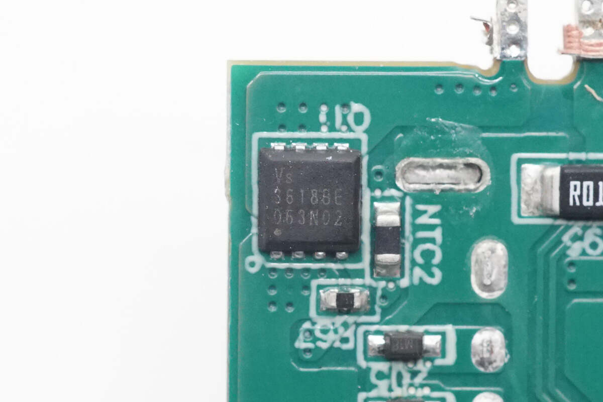
The three VBUS MOSFETs are from Vergiga and use the PDFN3333 package. 30V 5.2mΩ. Model is VS3618BE.
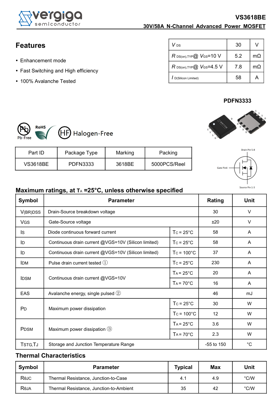
Here is the information about Vergiga VS3618BE.
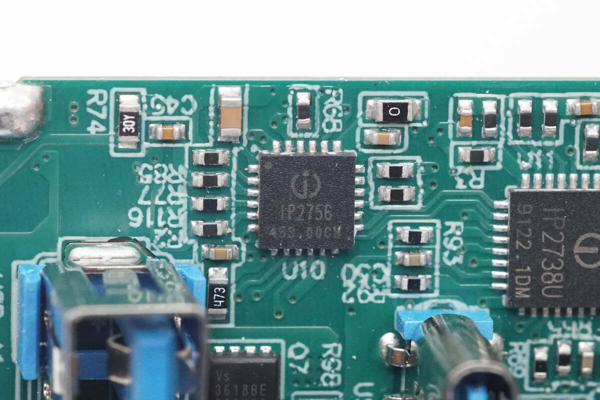
The protocol chip for the USB-A port is from Injoinic and adopts the QFN24 package. It is a fast charging protocol controller IC designed for USB ports, integrating support for multiple protocols including PD2.0, PD3.1 SPR & EPR 36V, HVDCP, QC5/4+/3+/3.0/2.0, VFCP, UFCS, Apple 2.4A, BC1.2, and Samsung 2.0A. It provides a complete solution for single-direction output applications such as adapters and car chargers. Model is IP2756.
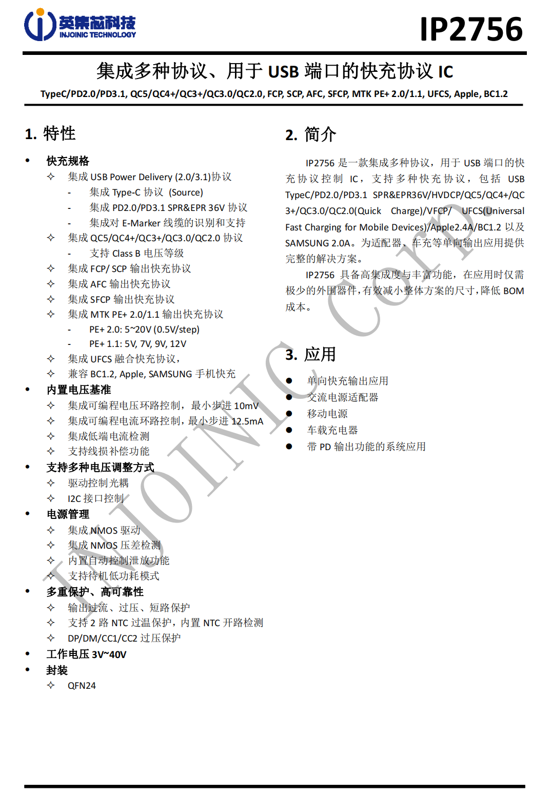
The IP2756 features high integration and rich functionality, requiring only minimal external components in the application. This effectively reduces the overall solution size and lowers the BOM cost.
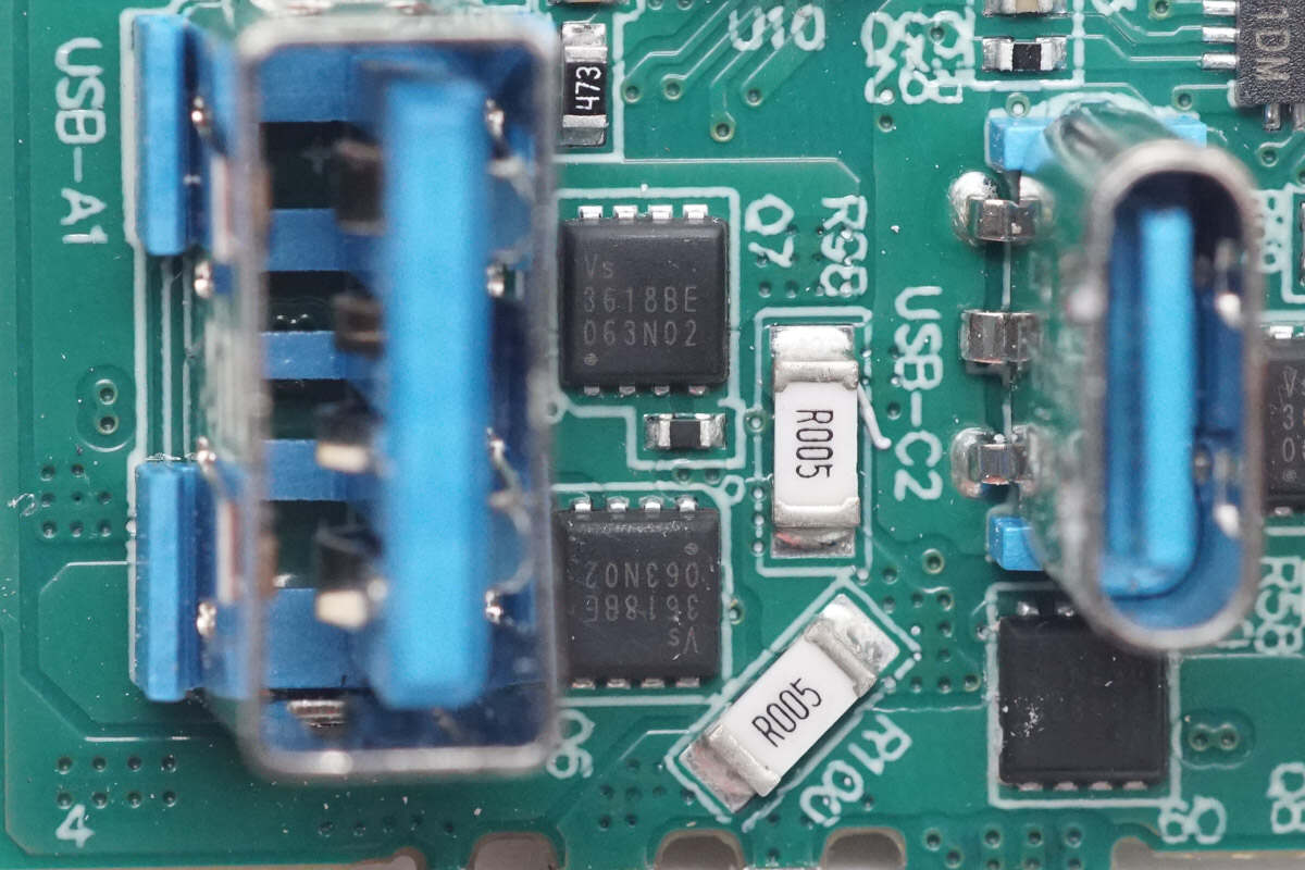
These two VBUS MOSFETs are from Vergiga. Model is VS3618BE.
There is also a VBUS MOSFET of the same model on the back.
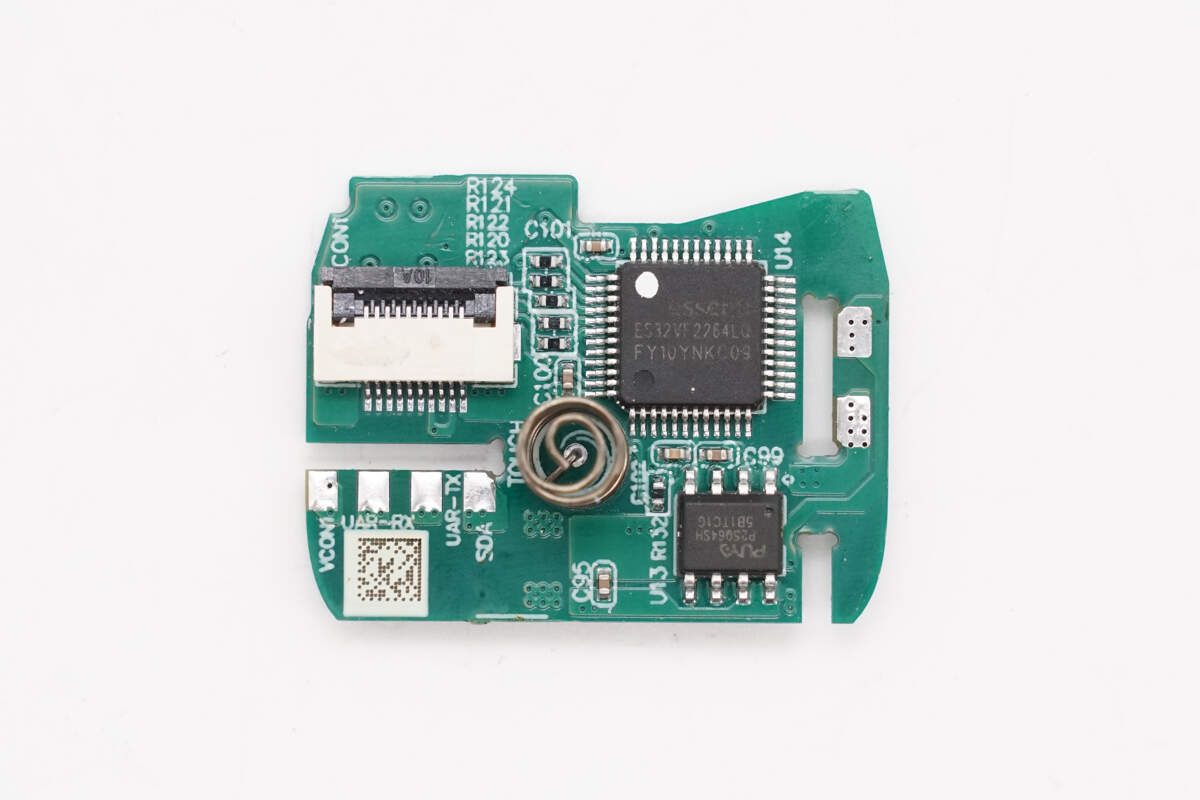
The small PCB of the display is equipped with an MCU and memory, as well as a screen flex cable connector and touch spring.
The back has a synchronous buck chip, a regulator, and a touch controller chip.
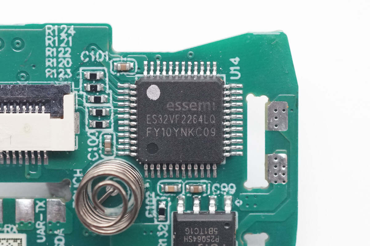
The MCU used to drive the display is from essemi and adopts the LQFP48 package. It features an E902 core with a main frequency of 72 MHz, and includes 256KB of FLASH and 32KB of SRAM. Model is ES32VF2264LQ.
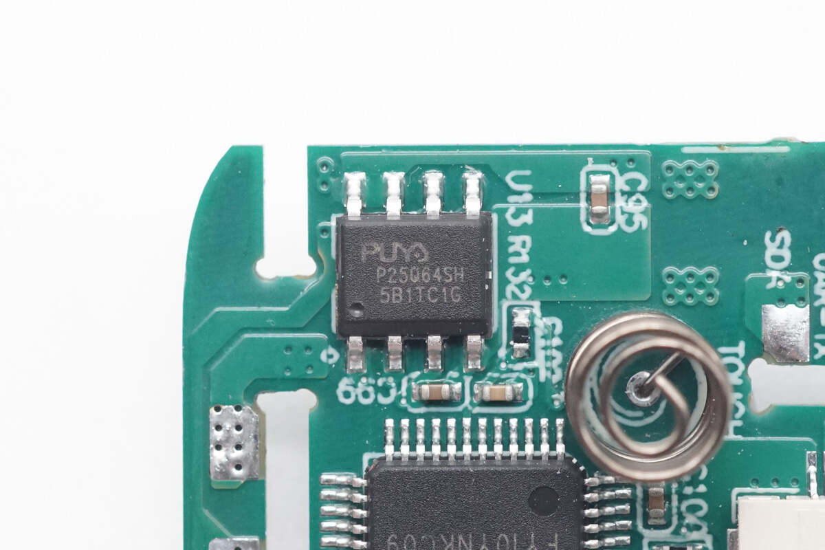
The external memory is from Puya and adopts the SOP8 package. The capacity is 8 MB. Model is P25Q64SH.
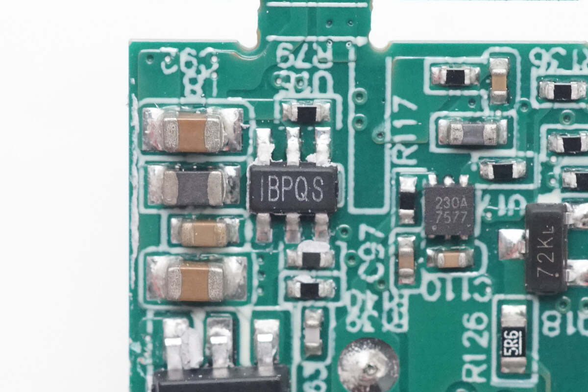
The synchronous buck converter marked BPQ is from MPS and adopts the TSOT23-6 package. It supports a 45V input voltage and an output current of 0.6A. The chip has an integrated MOSFET and operates at a switching frequency of 1.7MHz. Model is MP2460.
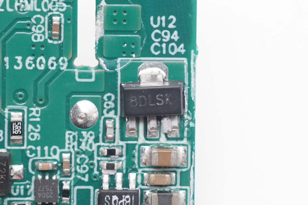
The regulator marked with 8DL is from LRC and adopts the SOT-89-3 package. It has an input voltage rating of 36V, an output voltage of 3.3V, and an output current of 250mA. Model is LR6375A33P.
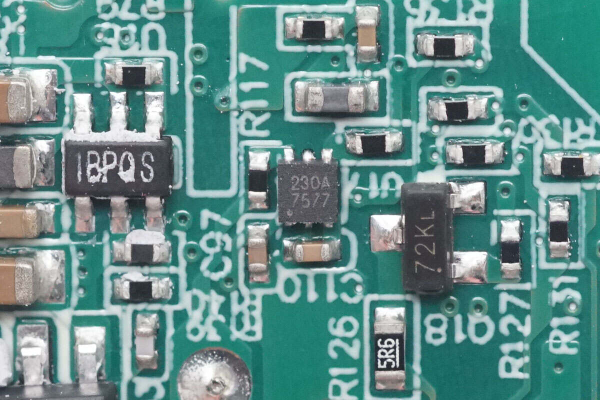
The touch controller chip marked with 230A is used for detecting touch.
Well, those are all components of the Anker GaNPrime Lite 100W Charger.
Summary of ChargerLAB
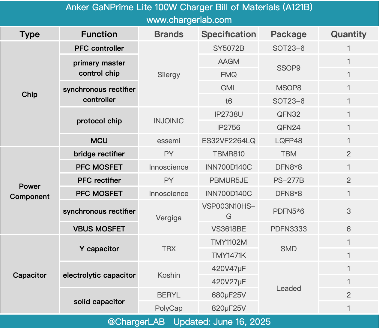
Here is the component list of the Anker GaNPrime Lite 100W Charger for your convenience.
It supports 100W output power and features two USB-C ports and one USB-A port. The USB-C ports support 100W output and are compatible with Xiaomi’s 90W proprietary fast charging protocol. Its LCD screen displays output power and temperature, allowing users to easily monitor the charging status.
After taking it apart, we found that it adopts a PFC + flyback topology. The PFC controller, master control chip, and synchronous rectifier controller are all from Silergy. The output uses Injoinic IP2738U and IP2756 for protocol control, and an Essemi MCU for the display. Heatsinks are installed on both sides of the PCBA module, and potting compound is applied internally to enhance thermal conduction and improve heat dissipation performance.
Related Articles:
1. Teardown of Original 60W PD Charger of Nintendo Switch 2
2. Teardown of vivo 90W FlashCharge GaN Charger (V9082L0E1-CN)
3. Teardown of Xiaomi 90W GaN Pudding Charger (MDY-18-EU)