Introduction
Today, we’re bringing you a teardown of the 90W GaN charger that comes standard with the Xiaomi 15 Pro. In addition to supporting Xiaomi’s proprietary 90W fast charging, the included USB-A to USB-C cable also supports 65W PD output. Next, let’s take it apart to see its internal components and structure.
Product Appearance
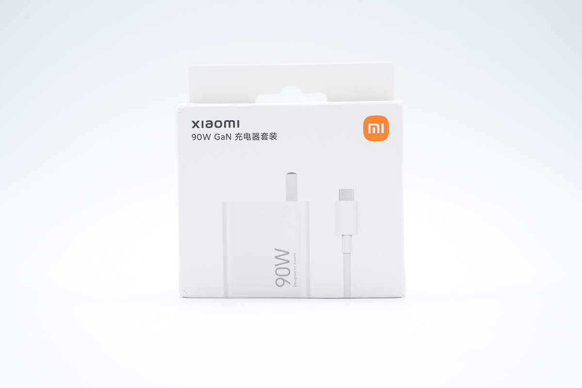
The front of the packaging features the Xiaomi logo, the product name, and an image of the charger set.

The back of the box has an information label.
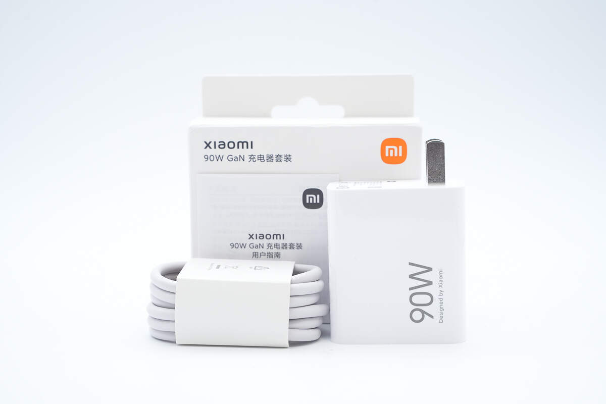
The package includes the charger, cable, and some documents.
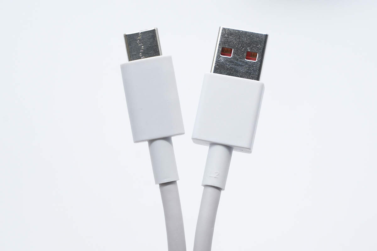
The USB-A to USB-C cable features a bend-resistant design.
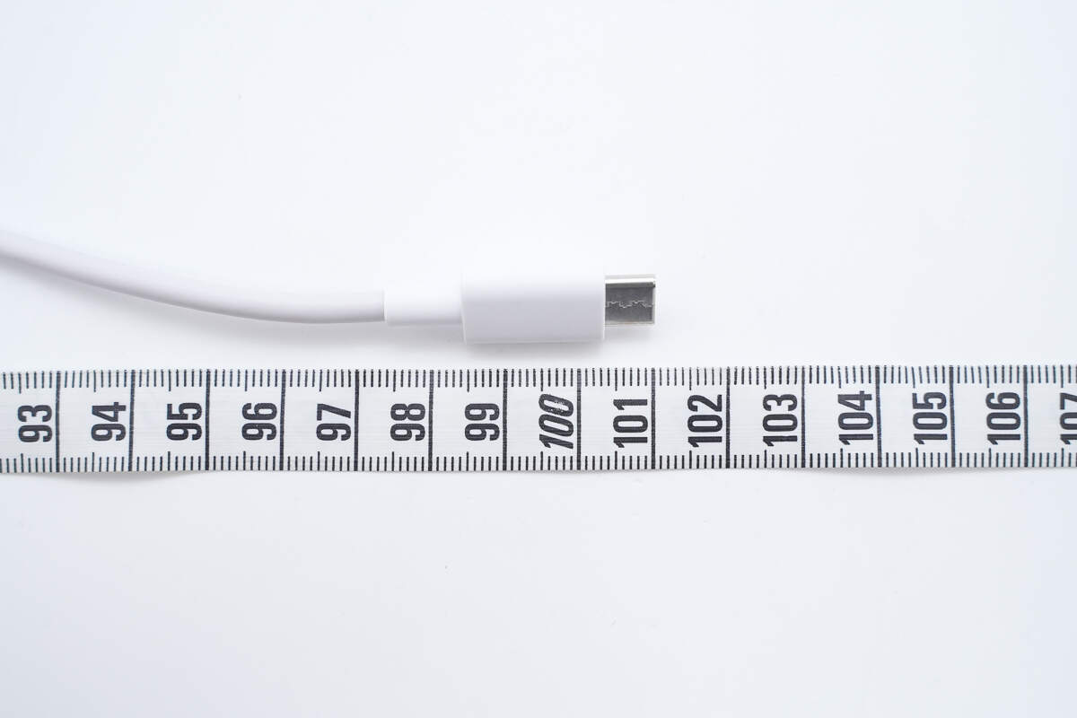
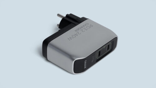
The length of the charger is about 1 m (3.28 ft).
It uses a flame-retardant PC casing with a glossy surface.
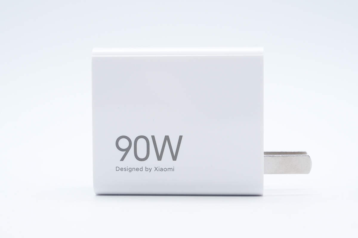
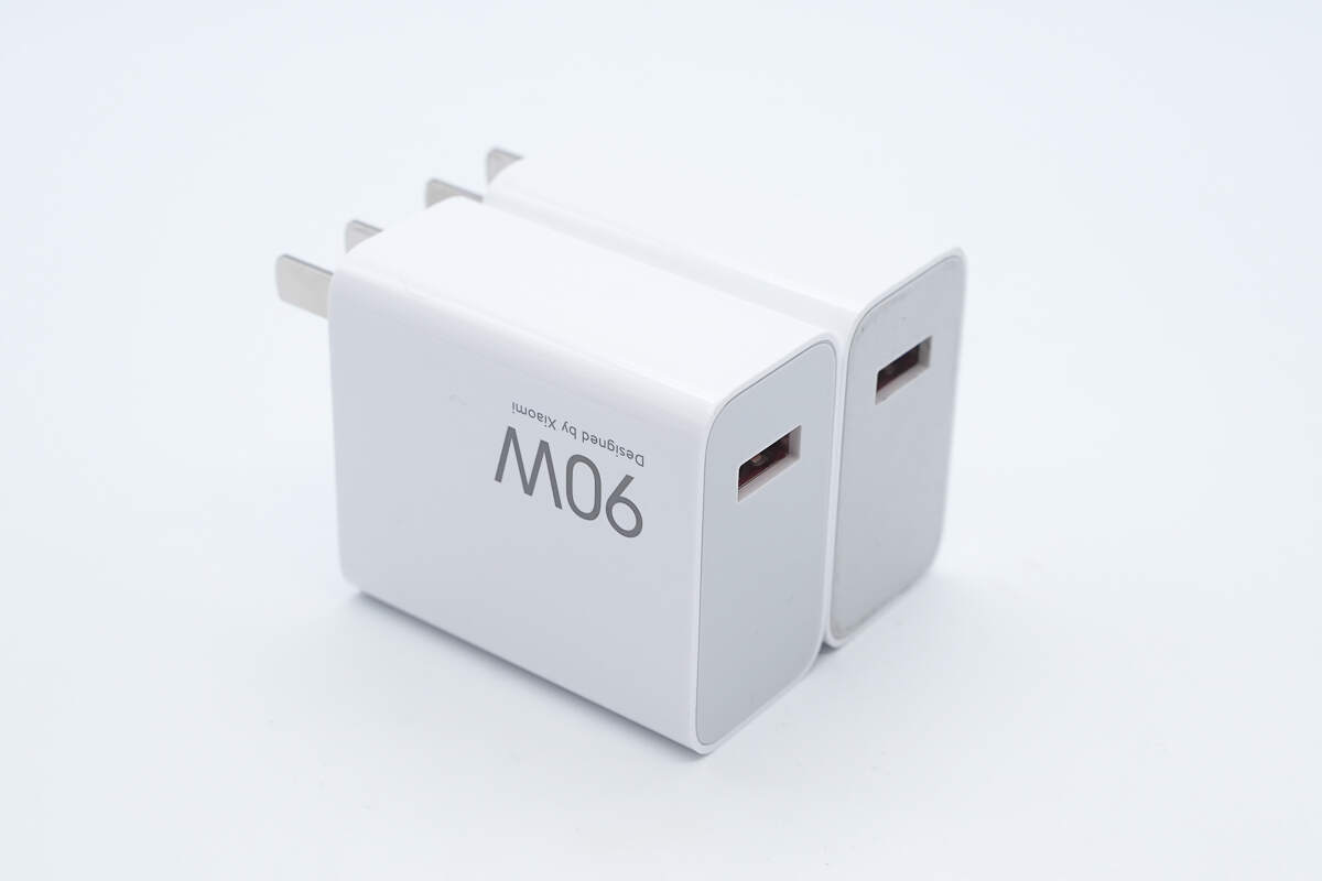
The front is printed with "90W" and "Designed by Xiaomi."
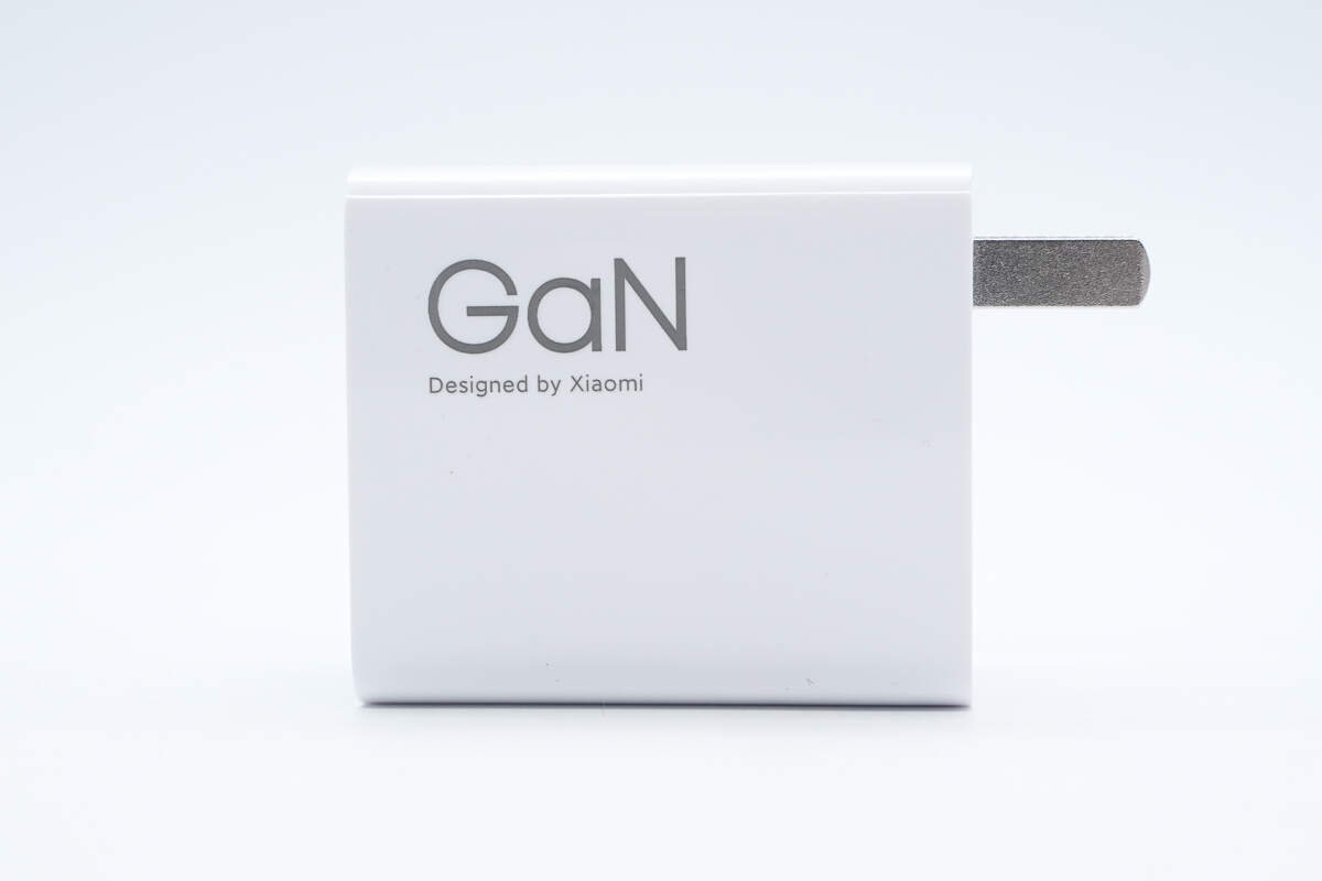
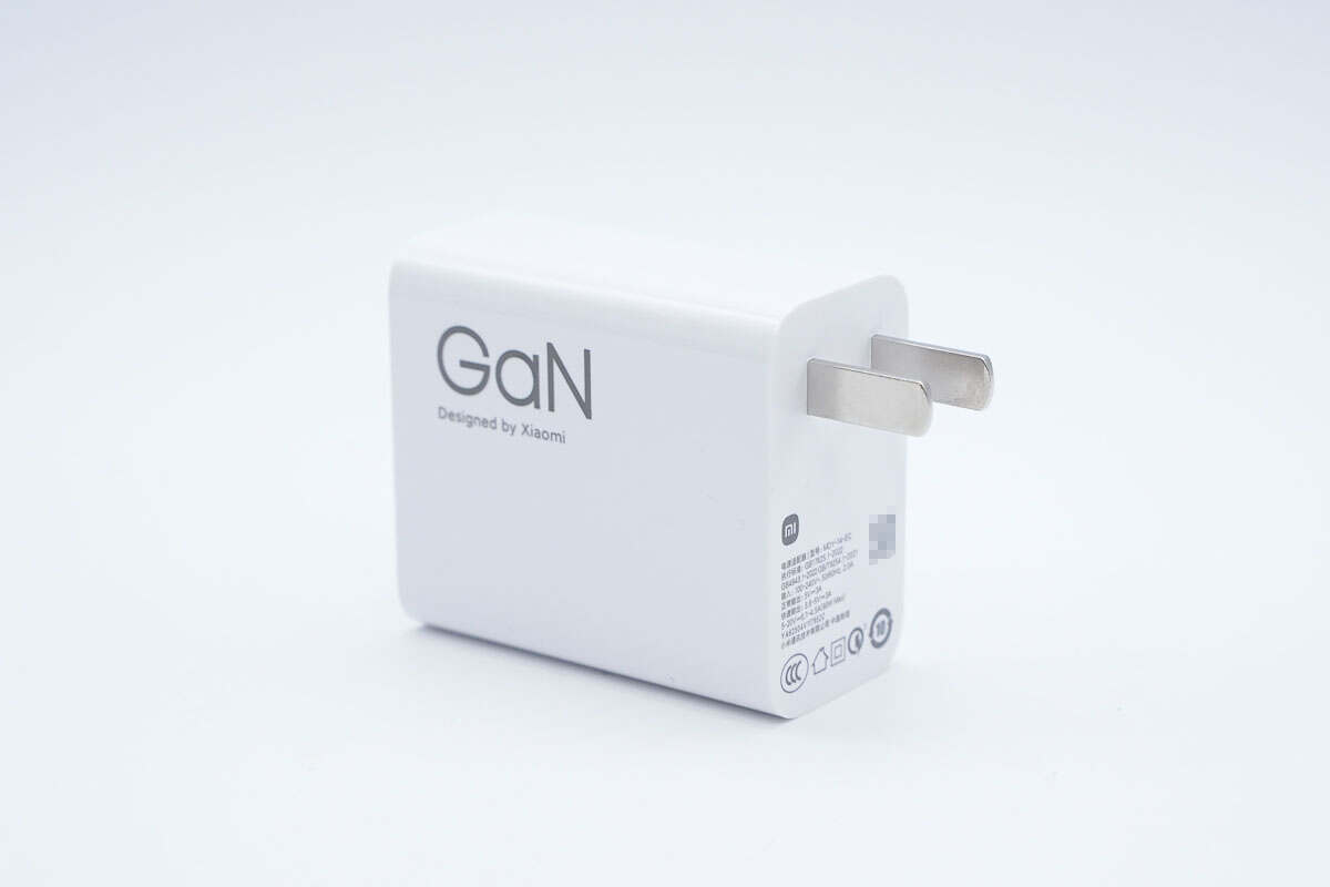
The other side is printed with "GaN" and "Designed by Xiaomi."
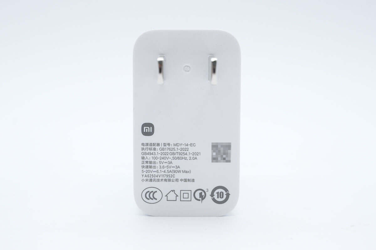
The input-side casing is printed with spec info.
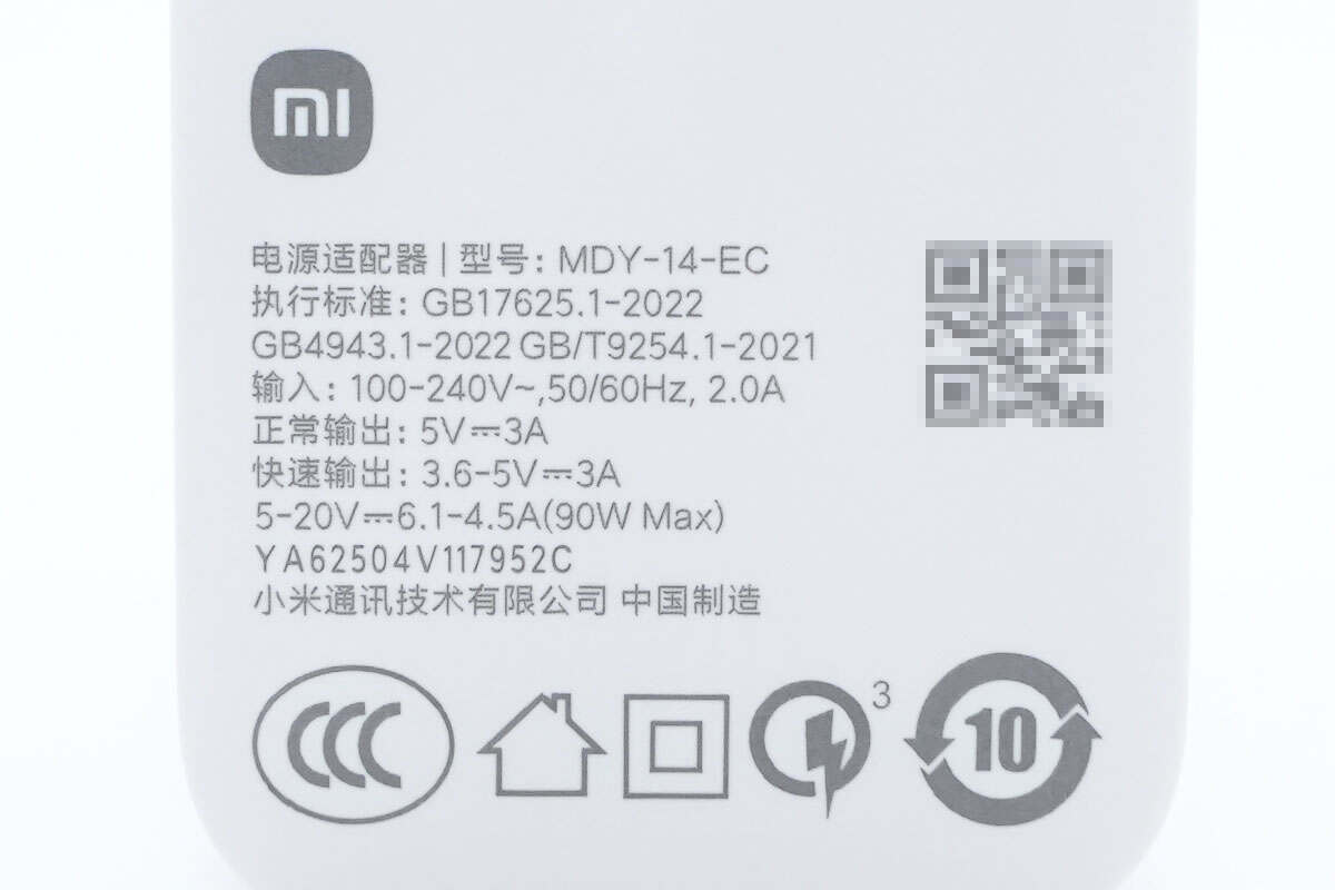
Model: MDY-14-EC
Input: 100-240V\~50/60Hz 2A
Standard Output: 5V 3A
Fast Output: 3.6-5V 3A, 5-20V 6.1-4.5A (90W Max)
It has passed the CCC certification.
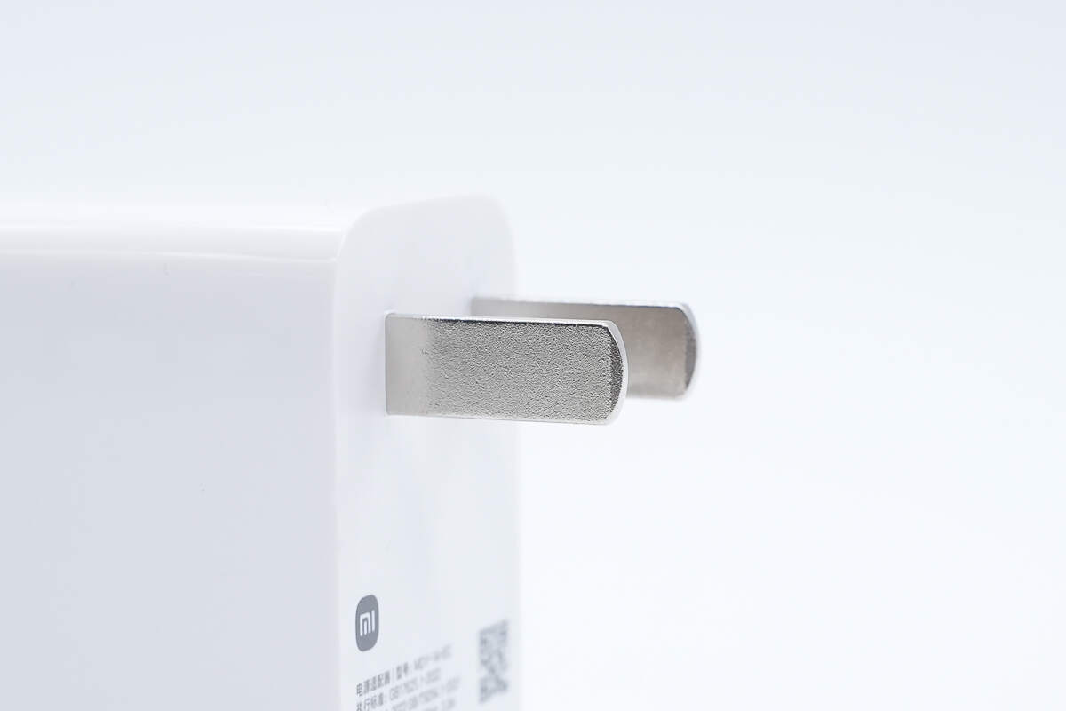
It is equipped with fixed prongs.

The USB-A plastic sheet is orange-red.
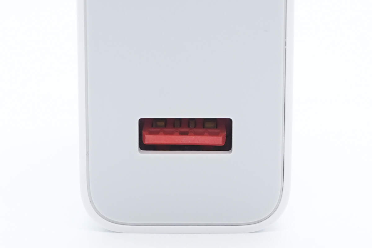
The front end of the plastic sheet has special contacts which, when used with the original cable, can achieve 65W PD output.
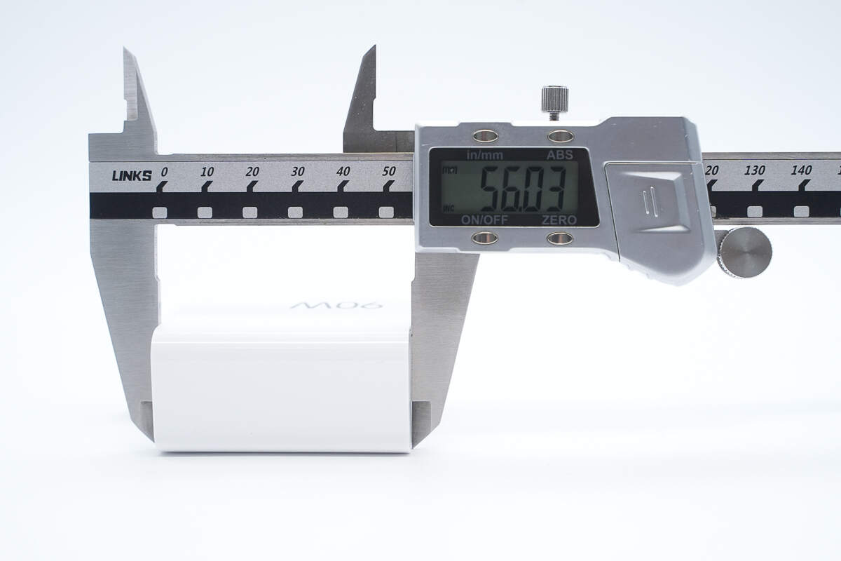
The length of the charger is about 56.03 mm (2.21 inches).
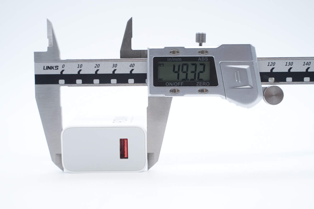
The width is about 49.32 mm (1.94 inches).
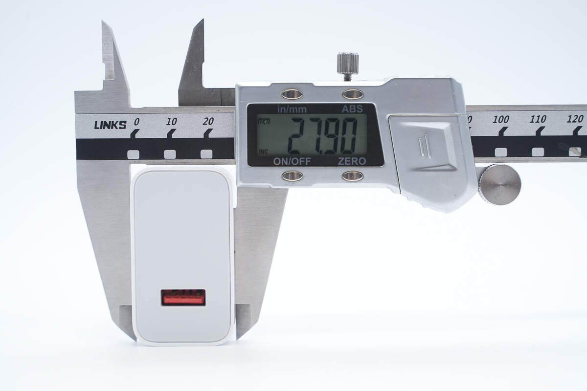
The thickness is about 27.9 mm (1.098 inches).
Compared to their previous generation 90W phone charger, the size remains unchanged.
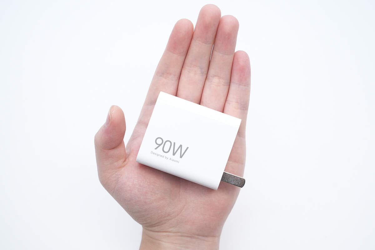
That's how big it is in the hand.
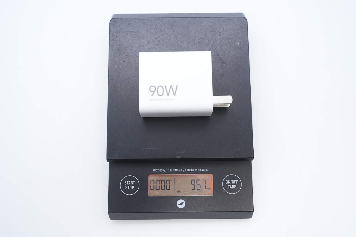
The weight is about 96 g (3.39 oz).
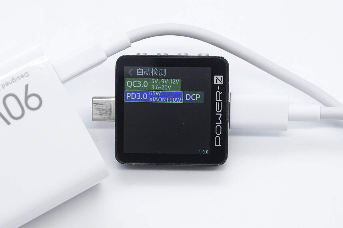
ChargerLAB POWER-Z KM003C shows that it supports QC3.0, PD3.0, and DCP charging protocols, as well as Xiaomi’s 90W proprietary protocol.
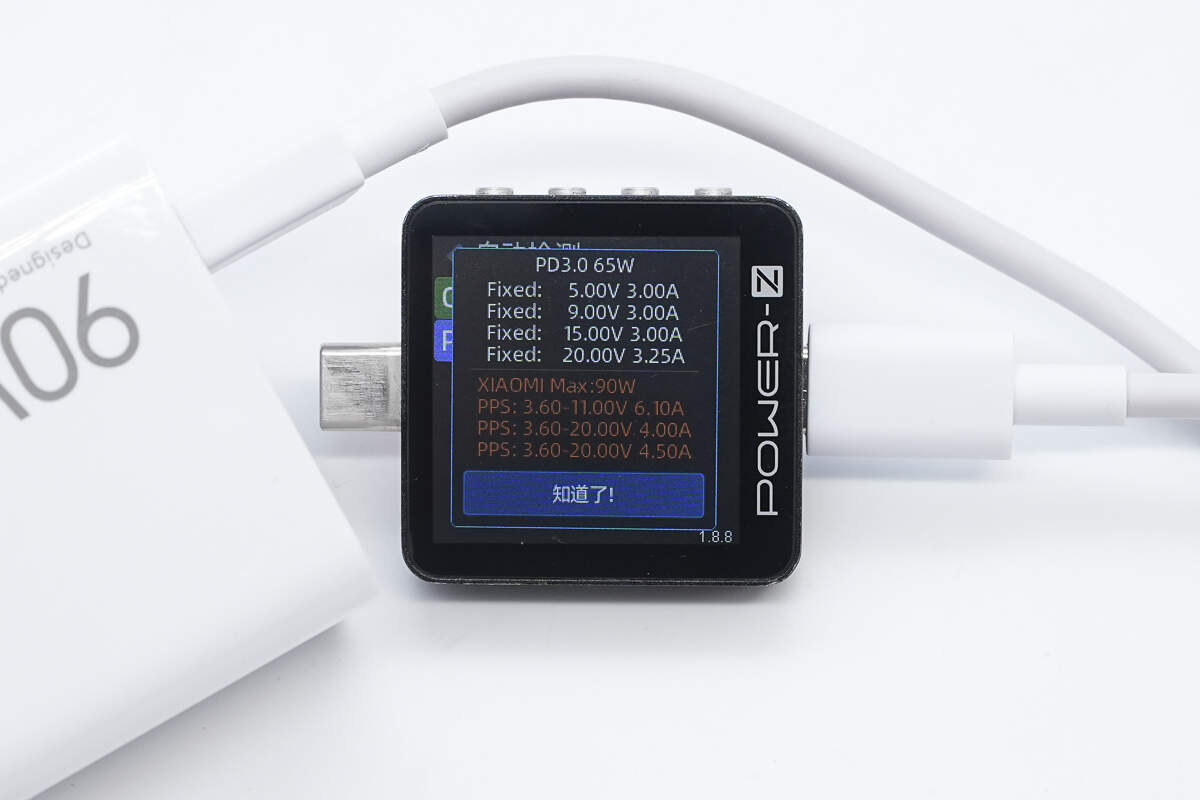
And it has four fixed PDOs of 5V3A, 9V3A, 15V3A, and 20V3.25A, as well as two Xiaomi proprietary voltage ranges: .6-11V6.1A, 3.6-20V4A, and 3.6-20V4.5A.
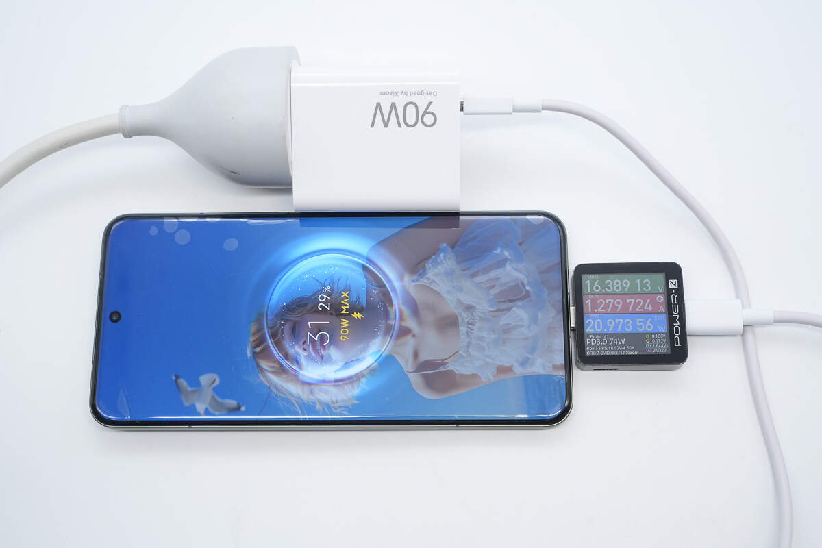
Using it to charge the Xiaomi 15 Pro successfully activates the 90W proprietary protocol.
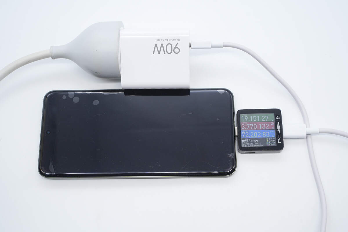
When the charging power climbs to a stable state, it is approximately 72.2W.
Teardown
Next, let's take it apart to see its internal components and structure.
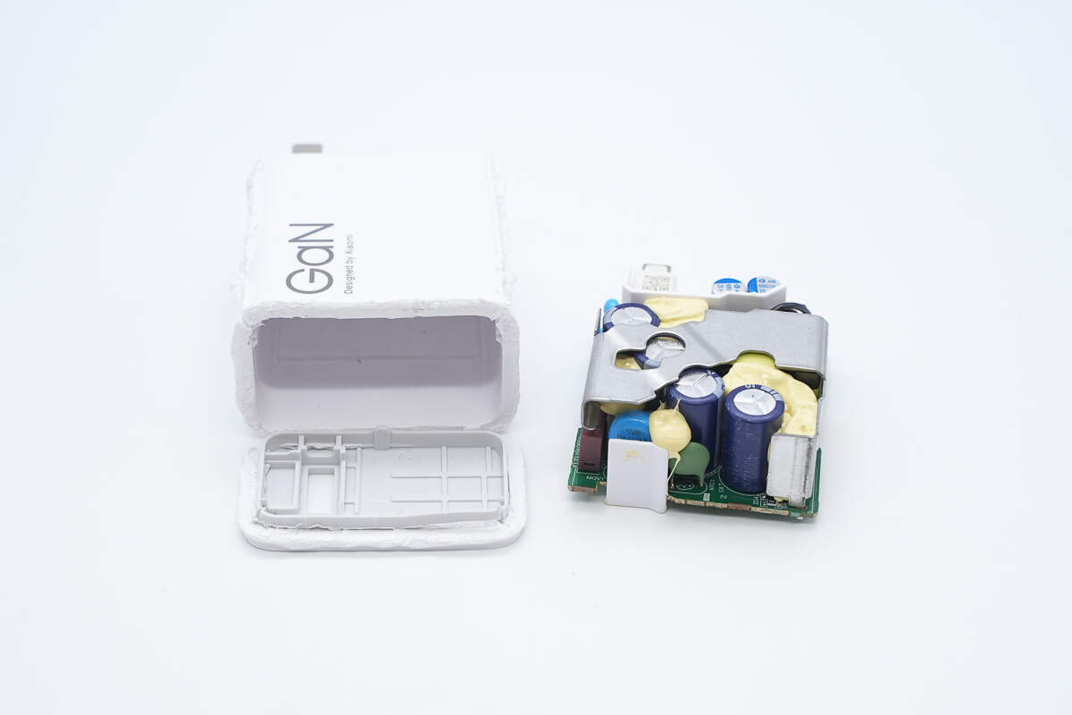
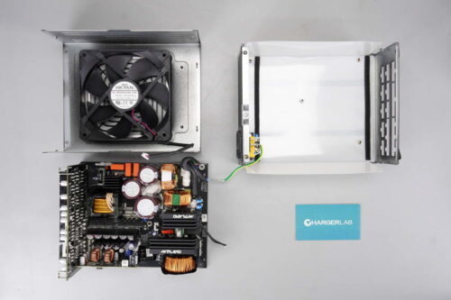
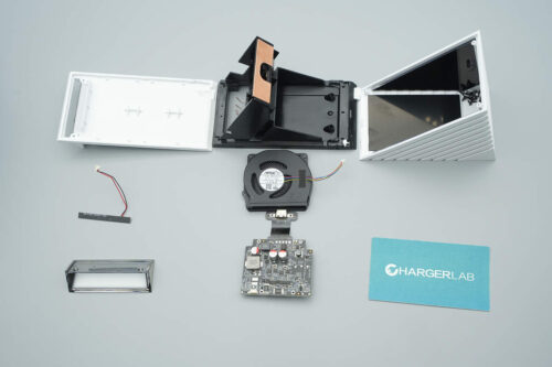
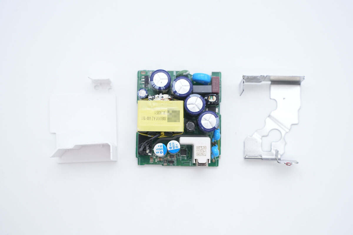
Cut open the casing to remove the PCBA module.
The input-side prongs and the PCBA module are connected by contact. The prongs are crimped with metal spring clips.
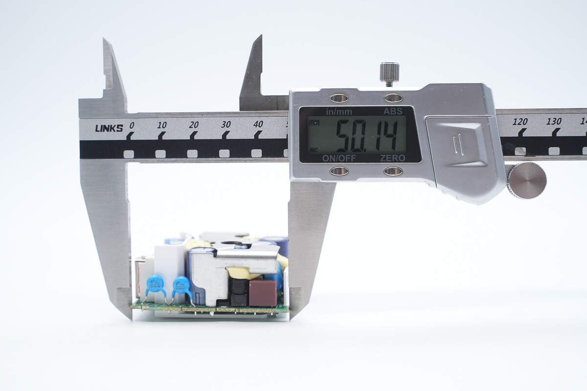
The length of the PCBA module is about 50.14 mm (1.97 inches).
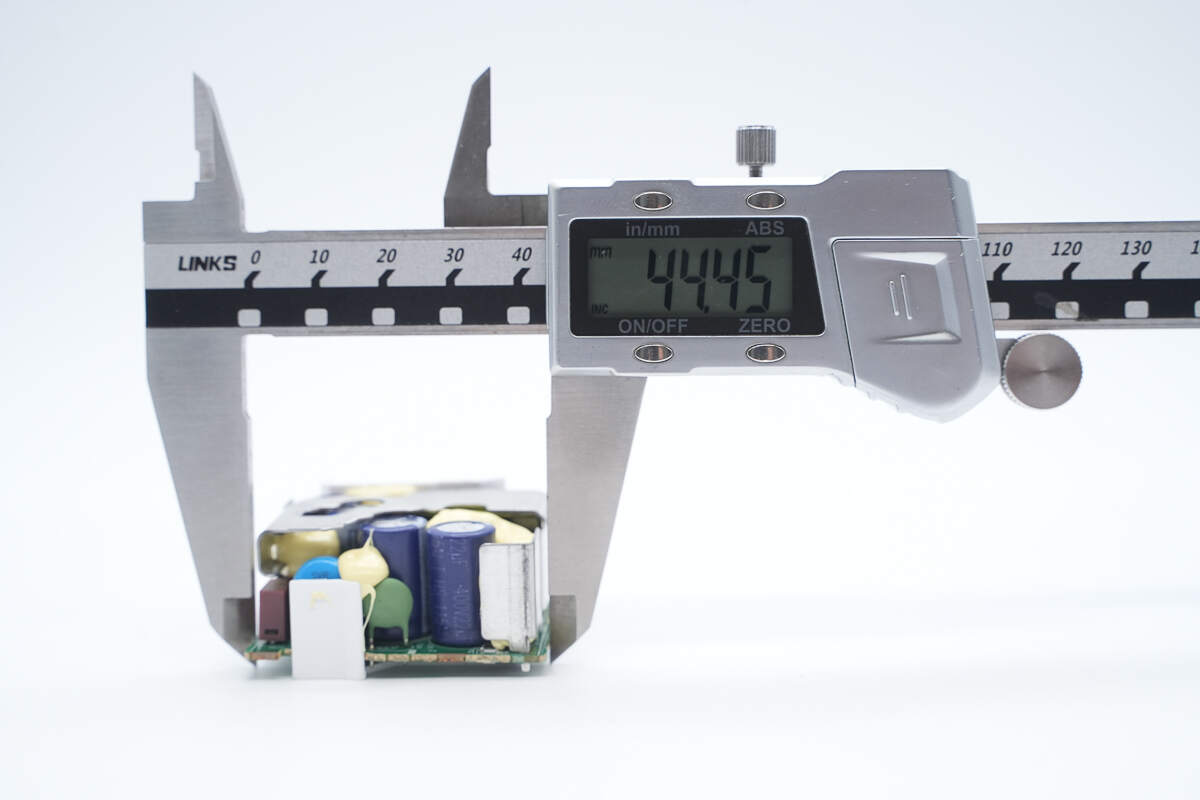
The width is about 44.45 mm (1.75 inches).
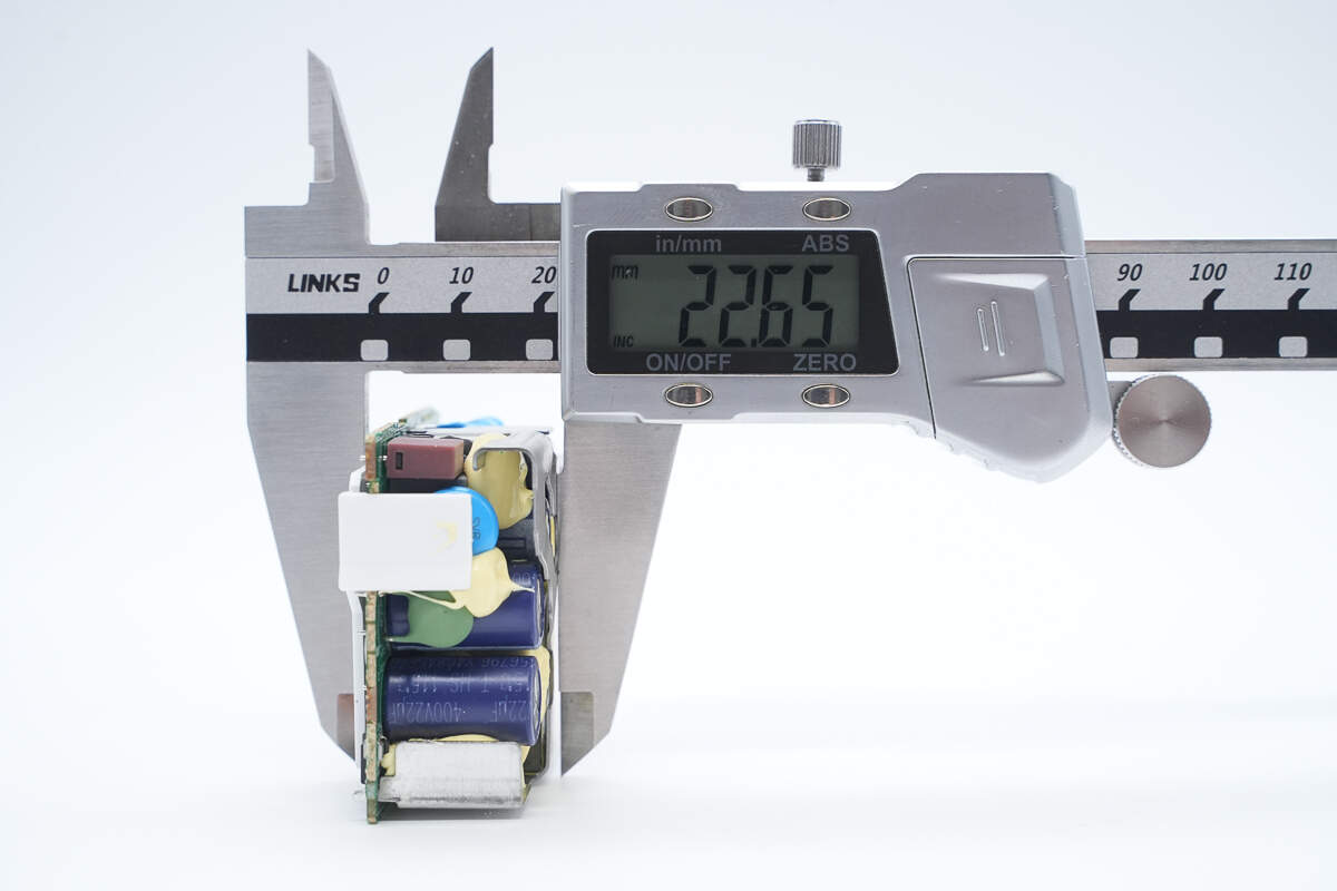
The thickness is about 22.65 mm (0.89 inches).
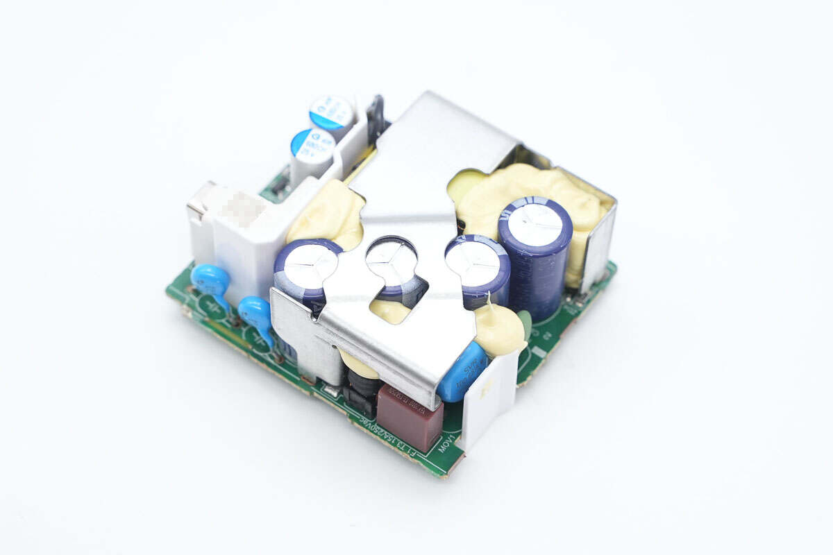
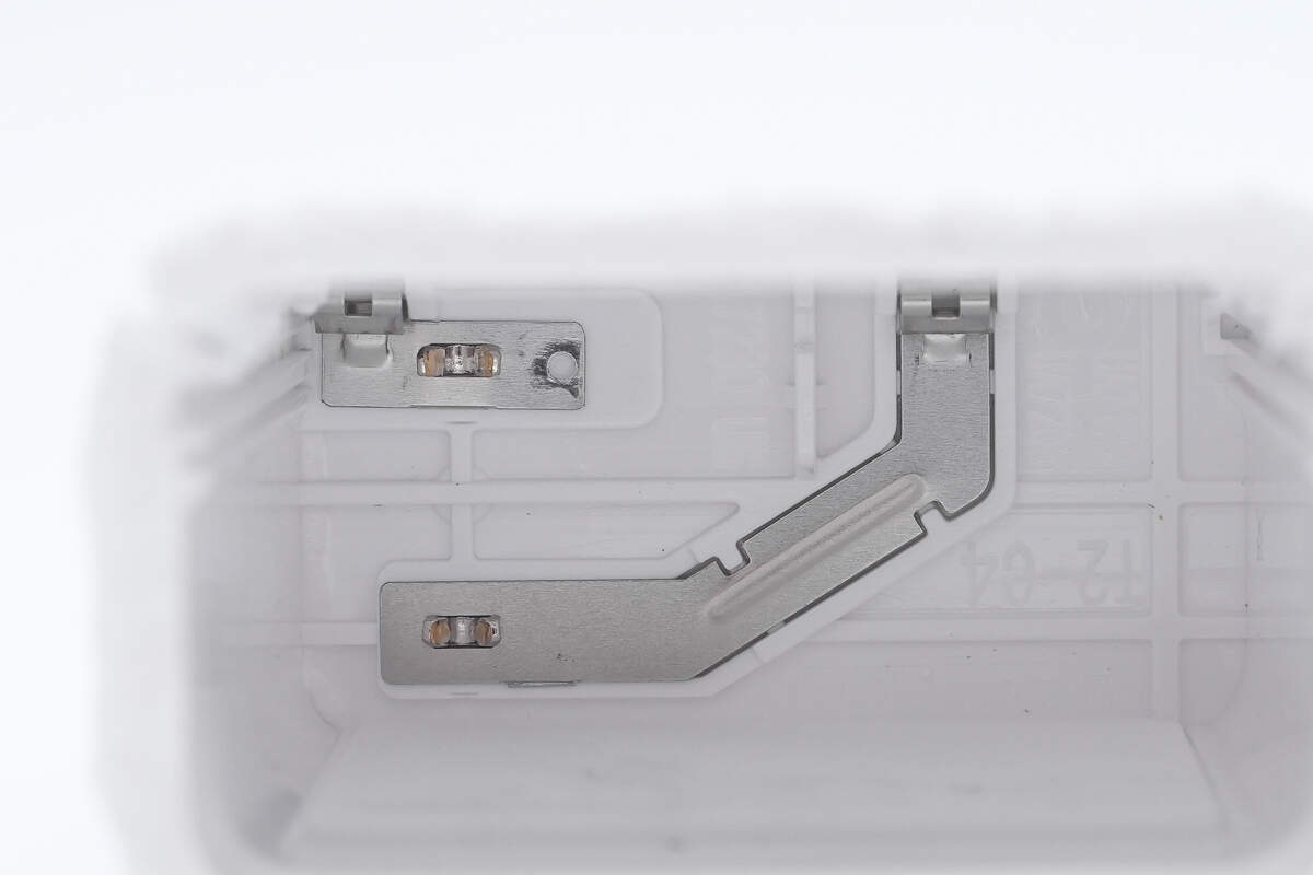
There is a plastic partition corresponding to the area of the delayed fuse, and a metal heat sink covers the top and both sides of the module.
There is also a plastic partition between the primary and secondary sides.
The back of the module is covered with a plastic plate and is covered with copper foil.
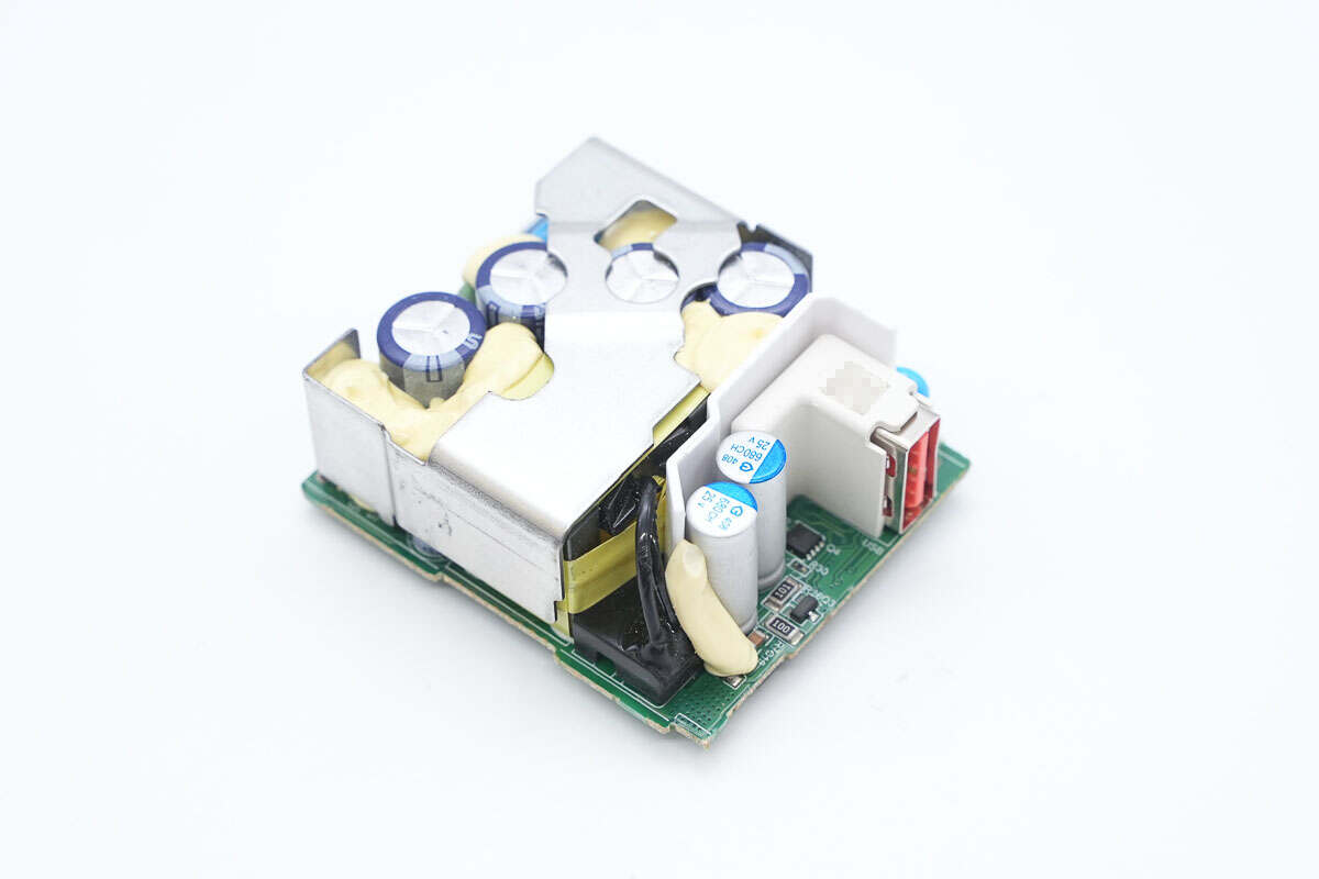
Remove the heat sink and the plastic plate.
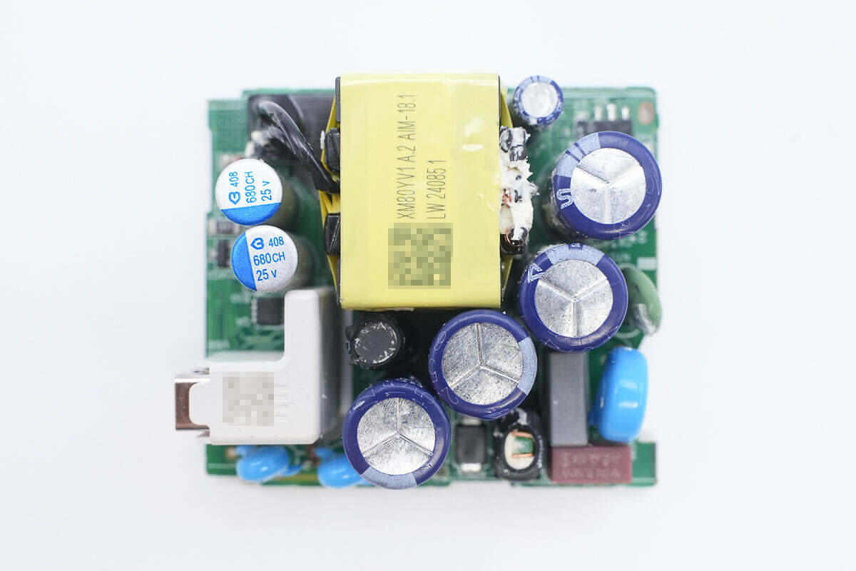
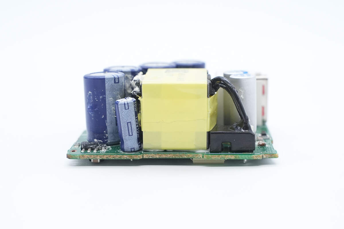
The front of the PCBA module has components such as a fuse, capacitors, and a transformer.
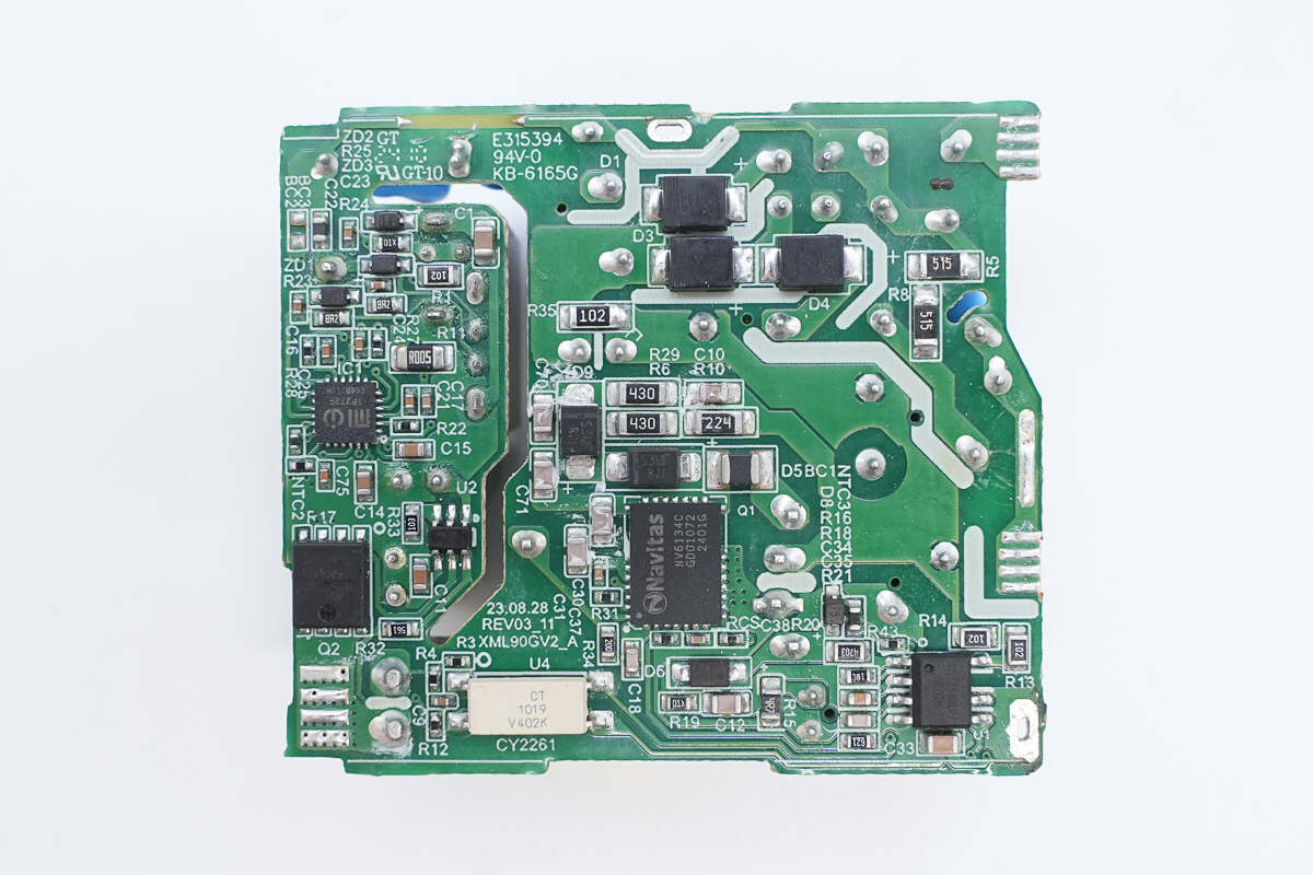
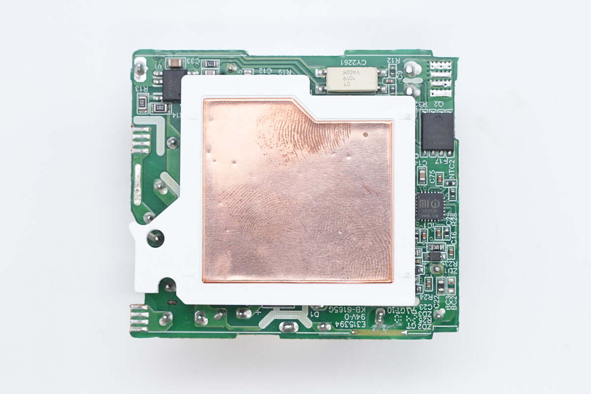
The back of the PCBA module contains components such as the master control chip, primary MOSFET, synchronous rectifier, and protocol chip.
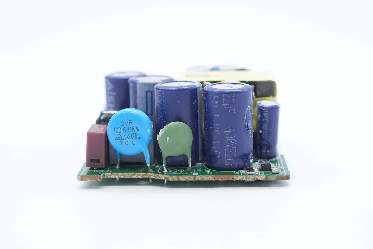
The front end of the PCBA module has a time-delay fuse, varistor, NTC thermistor, and electrolytic capacitors.
On the side, there are a safety X2 capacitor, a common mode choke, and two electrolytic capacitors.
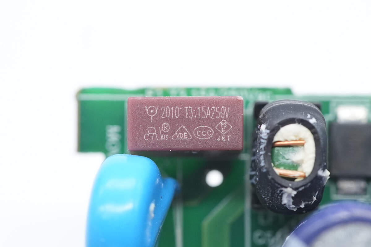
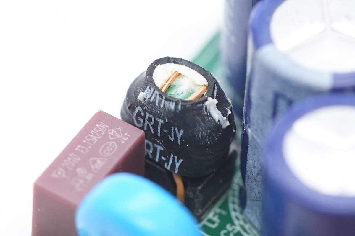
The time-delay fuse is from WalterFuse. 3.15A 250V.
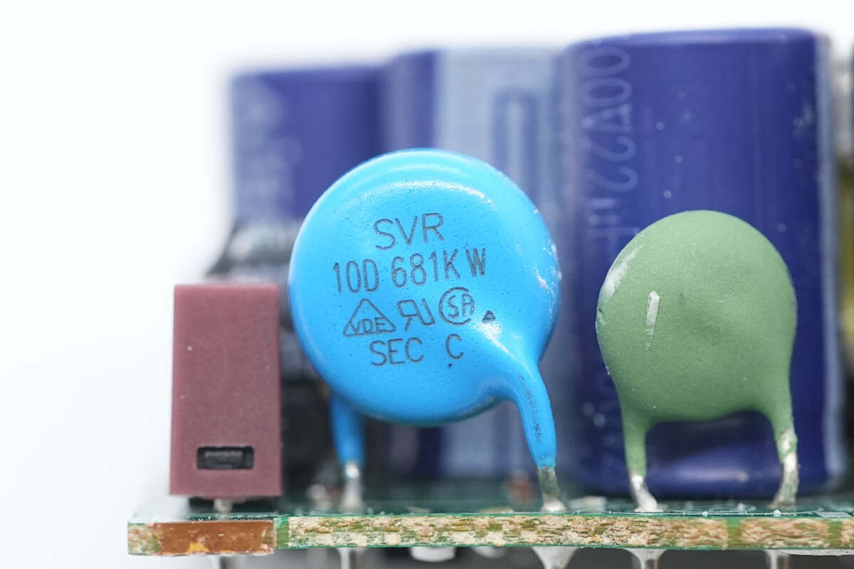
The varistor model is 10D681K, used to absorb surge overvoltage.
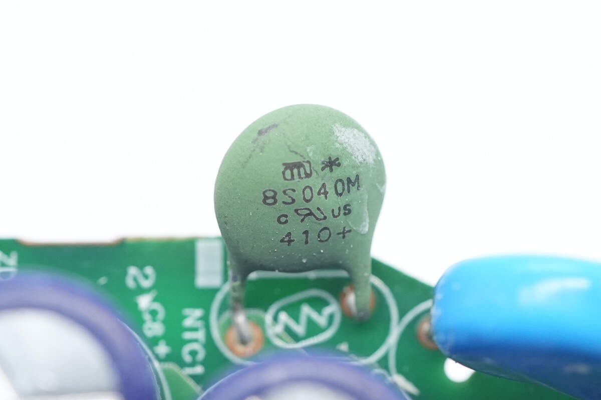
The NTC thermistor is used to suppress the inrush current when the charger is plugged in.
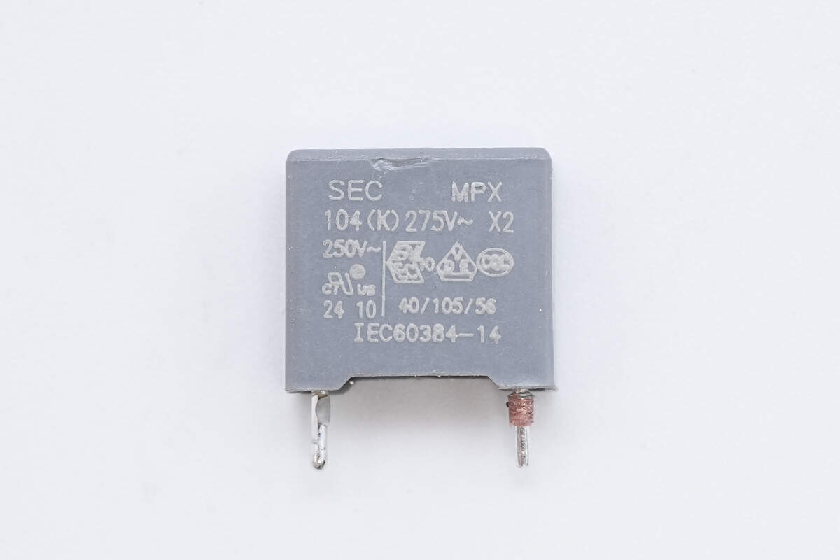
The safety X2 capacitor is from SEC. 0.1μF.
The common mode choke uses a toroidal winding, with an insulated base soldered underneath and covered with heat shrink tubing for insulation.
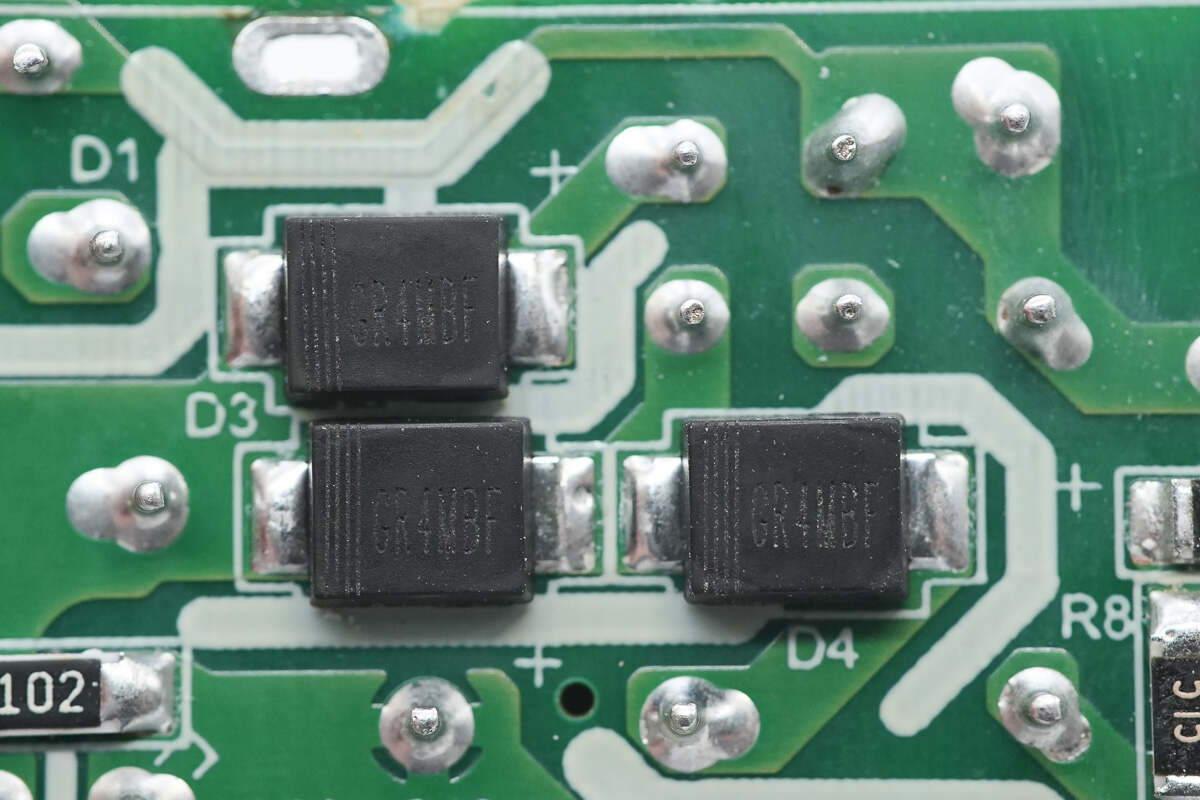
The bridge rectifier is made up of four diodes, three of which are located on the back side of the PCB.
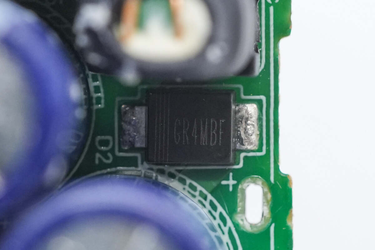
The fourth diode, model GR4MBF, is located next to the common mode choke. 4A 1000V.
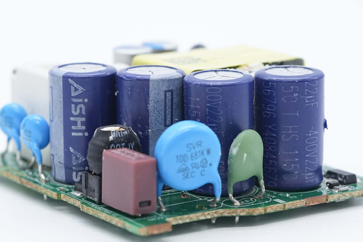
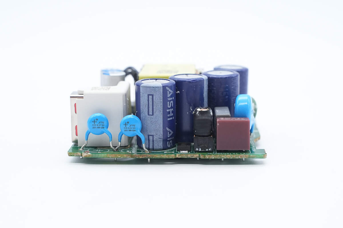
The four electrolytic capacitors are from AiSHi, each rated at 400V 22μF.
The differential mode inductor uses an E-core winding and is insulated with heat shrink tubing.
On this side, there is a capacitor that supplies power to the master control chip, as well as the transformer.
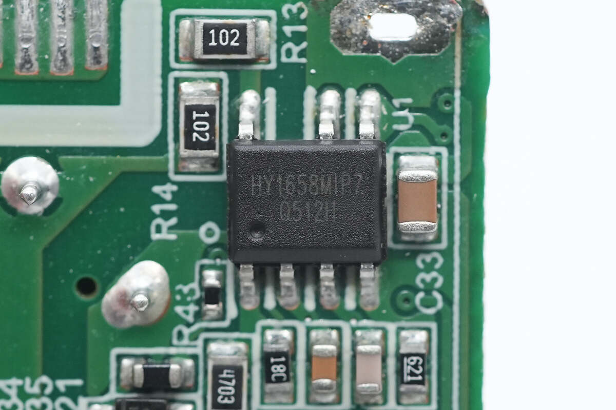
The master control chip is from HYASiC, model HY1658M. It is an intelligent multi-mode flyback controller featuring built-in high-voltage startup and support for multiple operating modes. It can automatically switch between QR and CCM to balance switching loss and conduction loss. It includes built-in frequency jittering to improve EMI performance, and an adaptive gate driver that balances switching loss and EMI. The driver output voltage clamp is set at 12V.
The HY1658M offers comprehensive protection functions, including output overvoltage protection, power supply overvoltage protection, transformer magnetic saturation protection, undervoltage/overvoltage protection, overload protection, over-temperature protection, and current sense resistor open-circuit protection. It is suitable for USB PD chargers, TV/monitor standby power supplies, and laptop power applications. The chip comes in an SOP7L package. Located at the lower left corner of the chip is an NTC thermistor, which provides internal over-temperature protection for the charger.
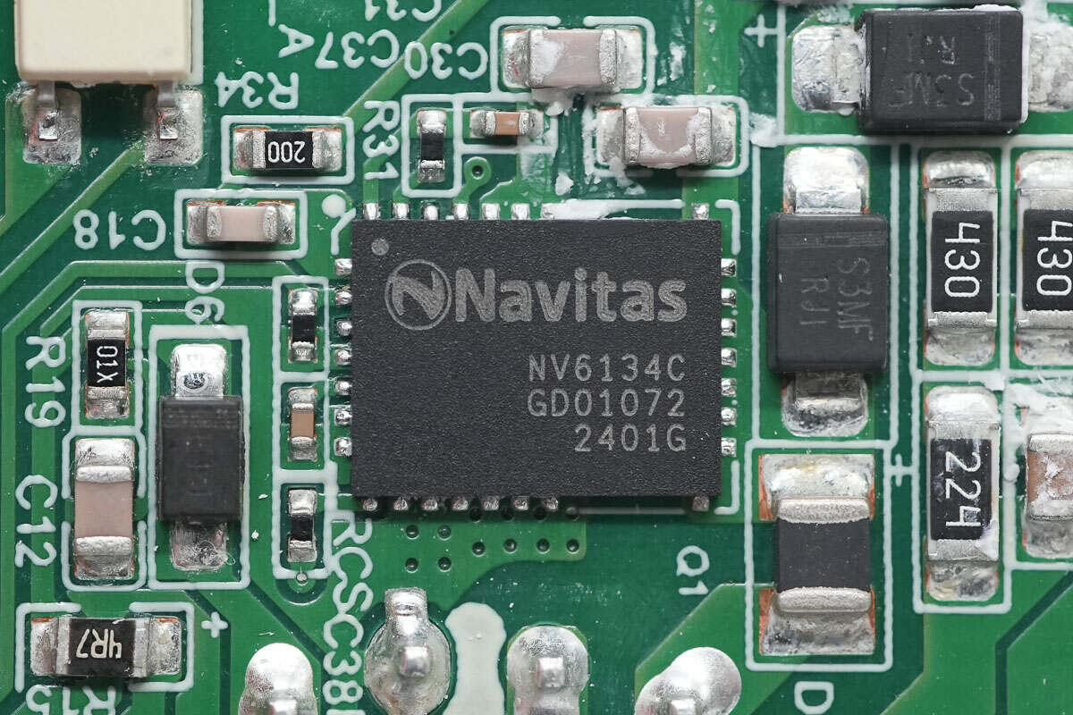
The primary MOSFET is the Navitas NV6134C, a highly integrated GaN power IC. It features a built-in driver and a high-precision, lossless current sensing circuit, eliminating the power loss associated with traditional sense resistors. The NV6134C integrates a 260mΩ GaN FET rated for 700V and supports switching frequencies up to 2MHz. It comes in a compact 6×8mm QFN package, helping to save board space.
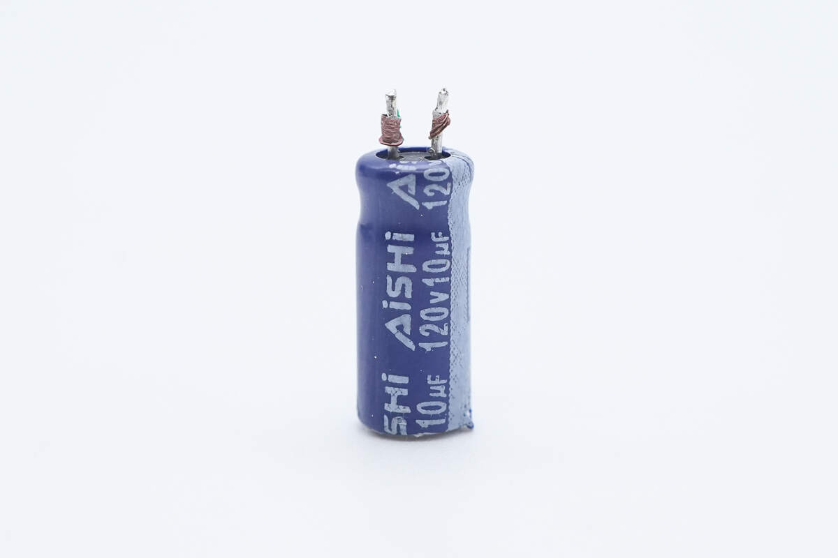
The capacitor that supplies power to the master control chip is also from AiSHi. 120V 10μF.
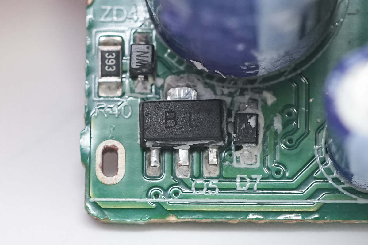
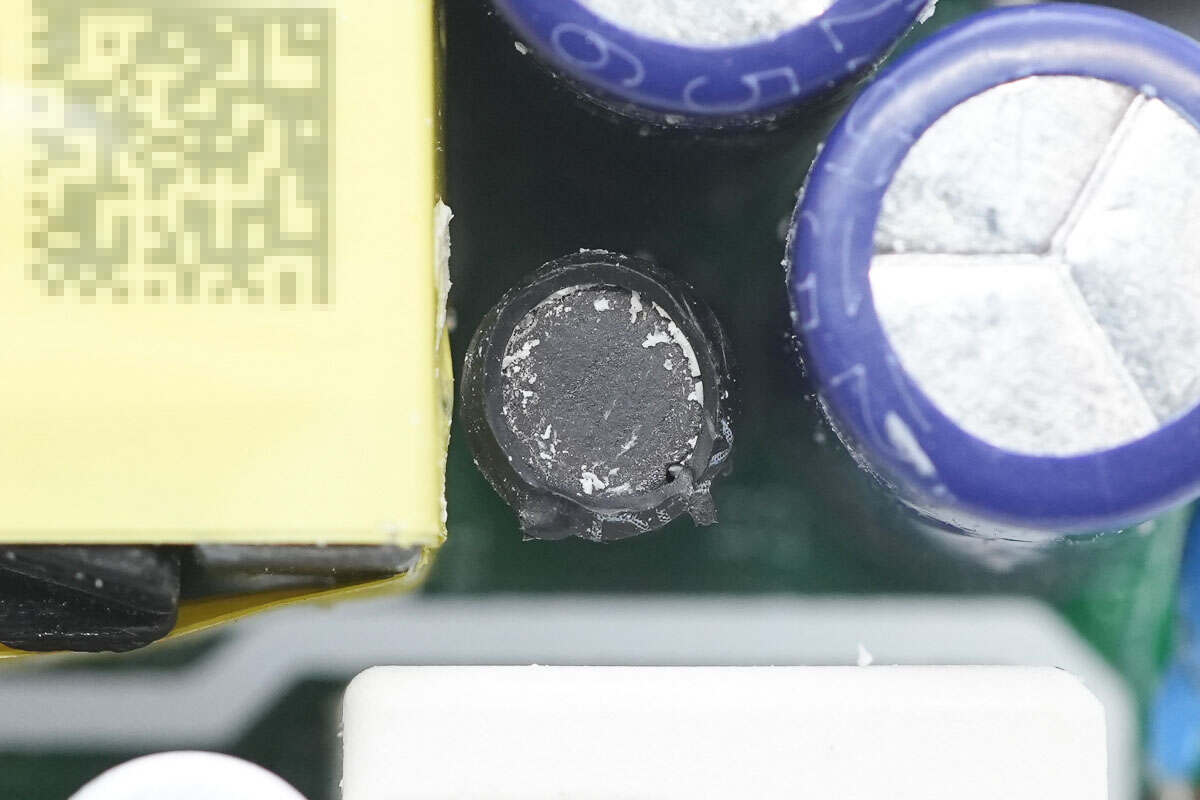
The transistor marked with "BL" is used for power supply voltage regulation.
Close-up of the transformer.
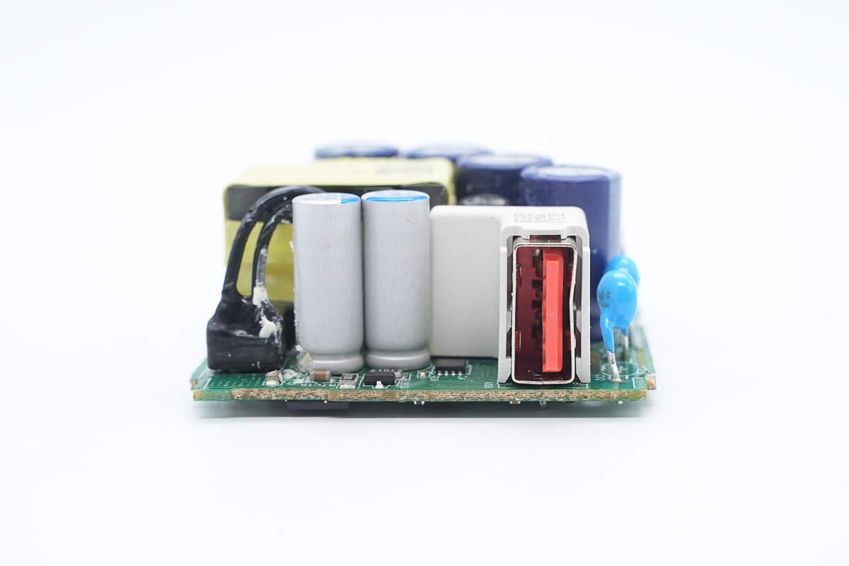
On this side, there are a USB-A socket, blue Y capacitors, solid capacitors, and a VBUS MOSFET.
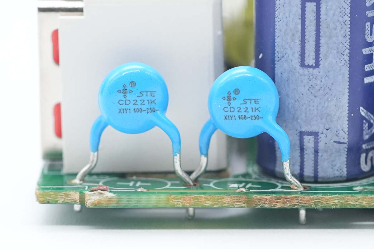
The two blue Y capacitors are from STE. After two 220pF capacitors are connected in series, the resulting capacitance is only 110pF, which keeps the leakage current between the primary and secondary extremely low, preventing any electric shock sensation upon contact.

The CT1019 optocoupler is used for output voltage feedback regulation.
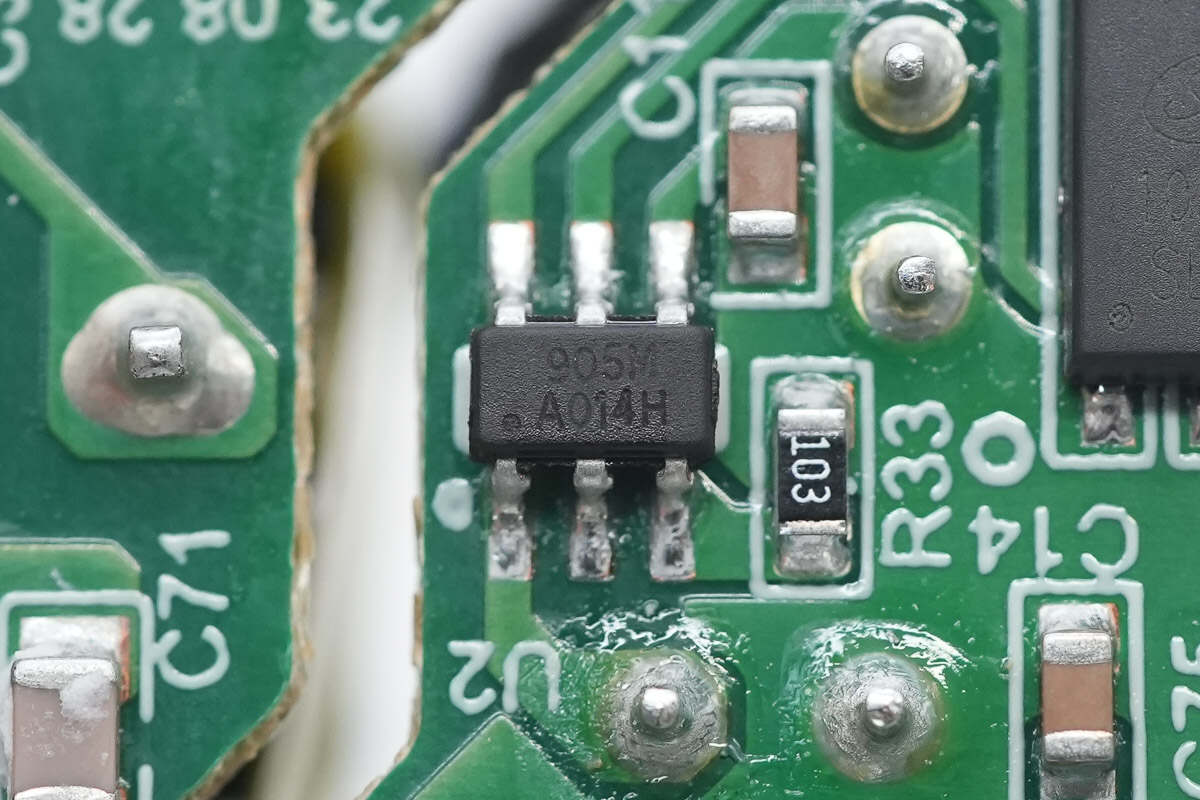
The synchronous rectifier controller is from HYASiC, model HY905M. It is a digital adaptive multi-mode synchronous rectifier controller that supports low-side applications without requiring an auxiliary coil for power. It supports multiple operating modes, including DCM, CCM, PFM, and QR. The supply voltage range is 3.2–25V, with a drive voltage clamp at 7.4V. It features high current output capability, is compatible with various synchronous rectifiers, and includes adaptive pre-shutdown driving to accelerate turn-off transitions. The controller comes in a SOT23-6 package.
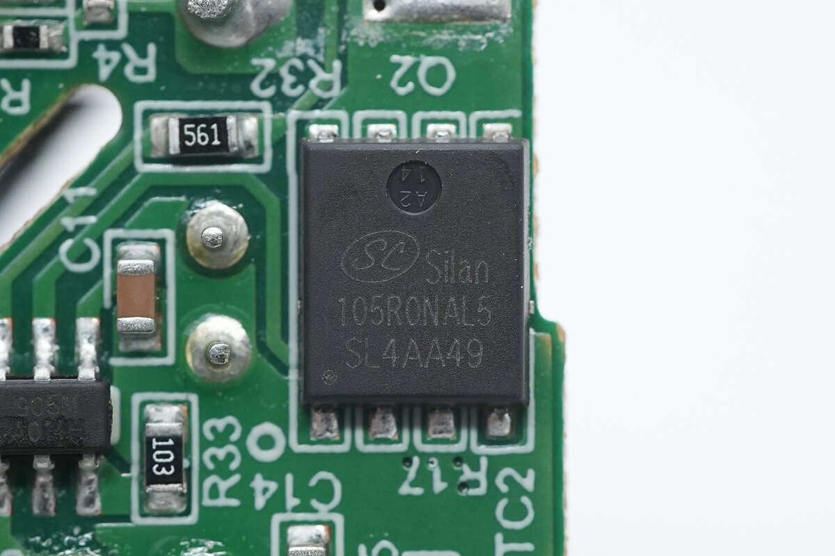
The synchronous rectifier is from Silan, model SVG105R0NAL5. It is a 100V-rated NMOS with an on-resistance of 3.8mΩ, packaged in a PDFN5×6-8 form factor.
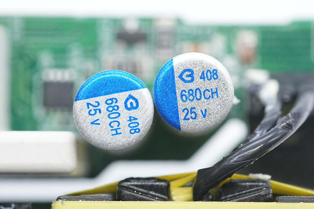
The two solid capacitors are from BERYL, CH series, each rated at 25V 680μF.
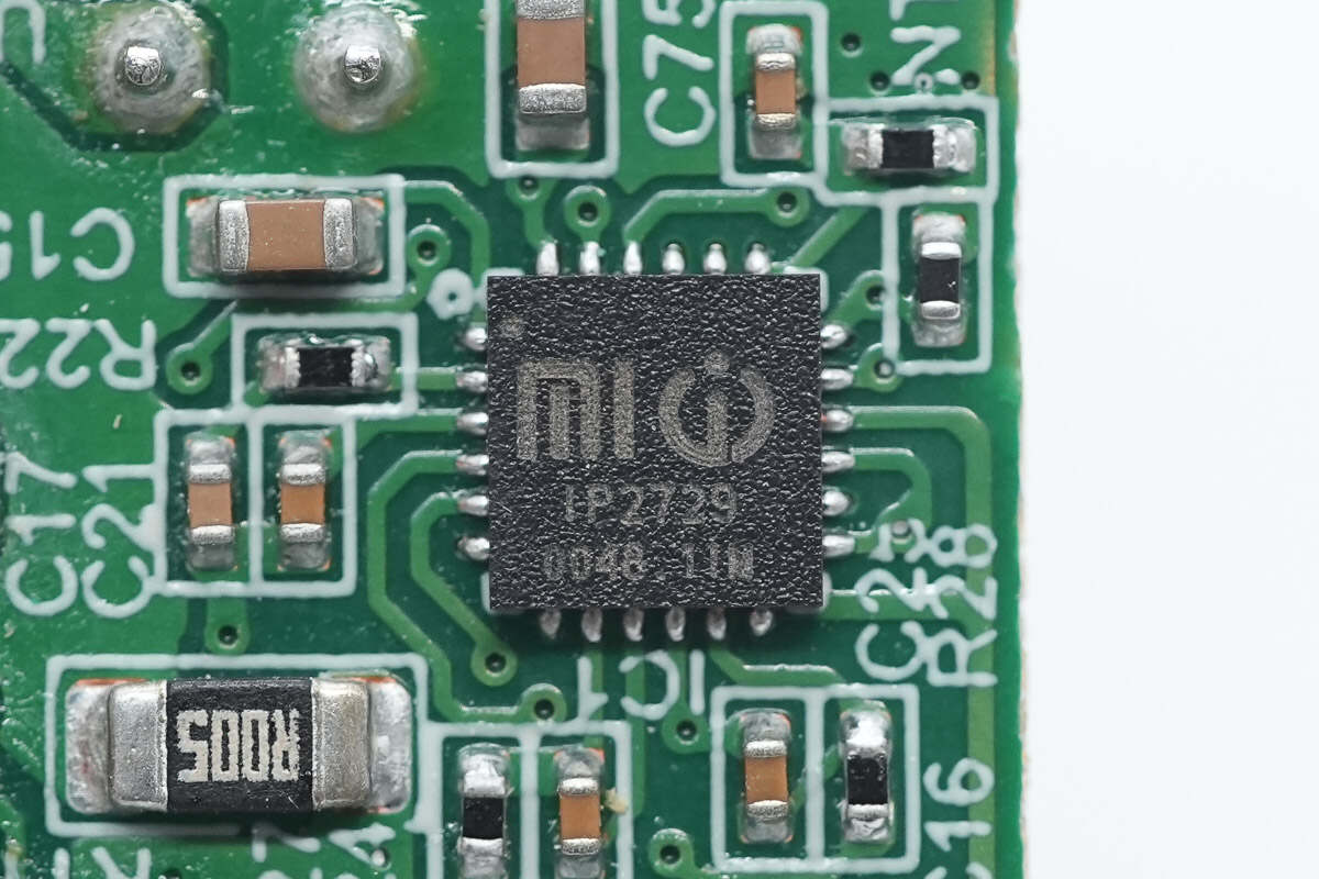
The protocol chip is from Injoinic, model IP2729. It is a Xiaomi-customized protocol chip that integrates USB PD, QC 3.0 fast charging, and Xiaomi’s 120W proprietary protocol, offering very powerful functionality. To the right of the protocol chip is a thermistor used to monitor internal temperature rise and provide overheat protection for the charger.
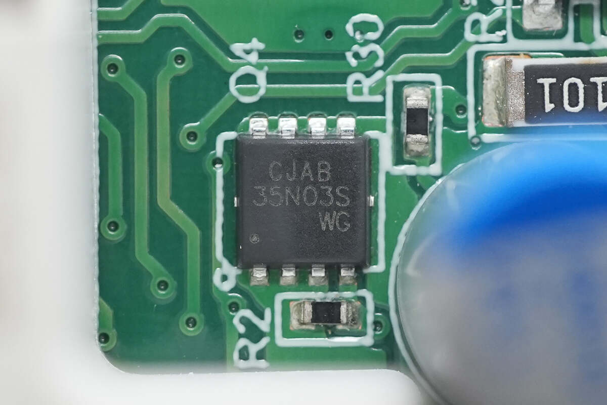
The VBUS MOSFET is from JSCJ, model CJAB35N03S. It is an NMOS with a voltage rating of 30V and an on-resistance of 5.2mΩ, housed in a PDFNWB 3.3×3.3-8L package.
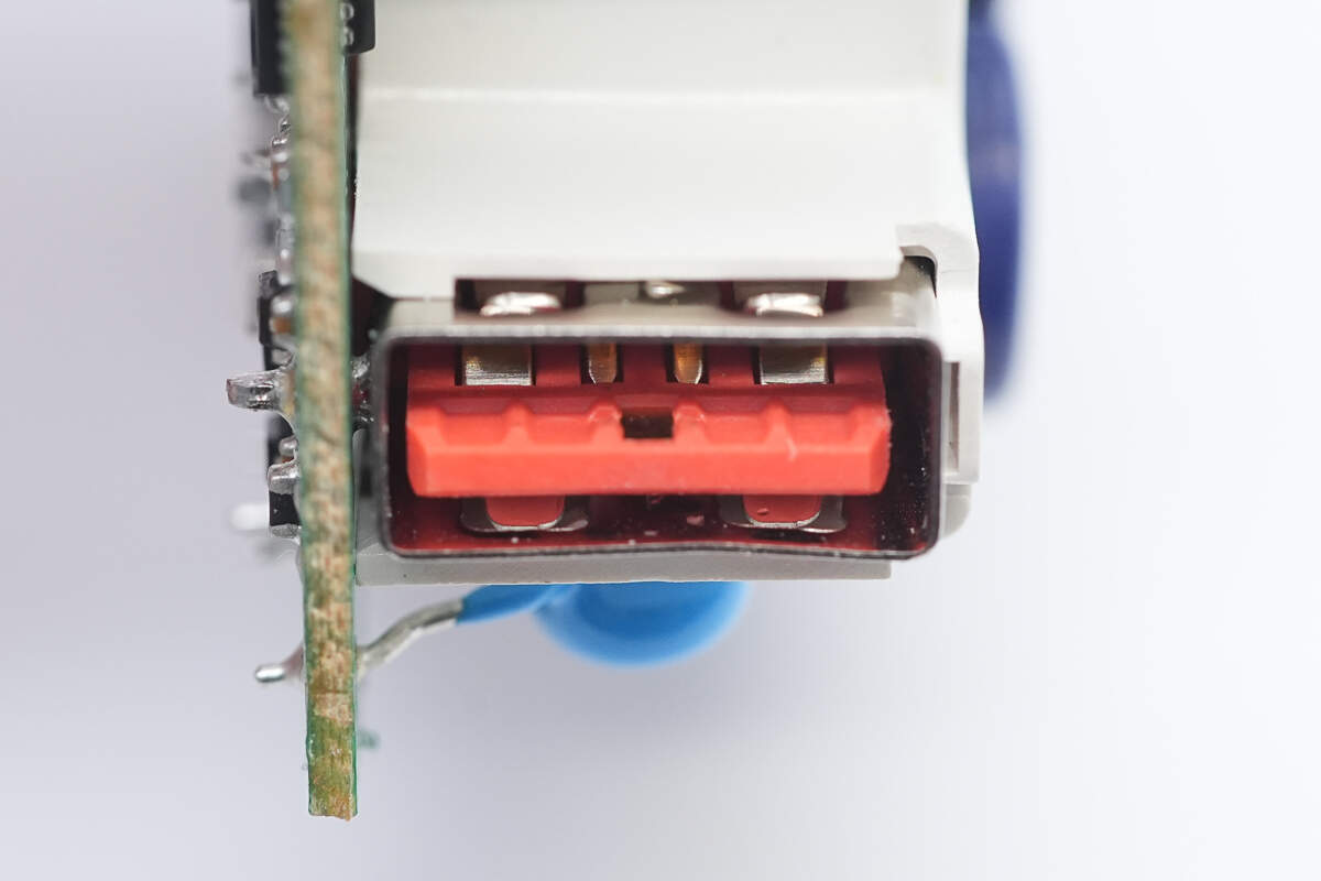
Close-up of the USB-A socket.

Well, those are all components of the Xiaomi 15 Pro 90W GaN Charger.
Summary of ChargerLAB
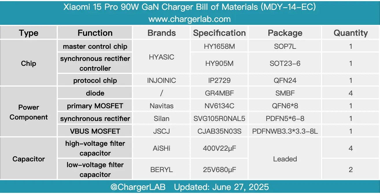
Here is the component list of the Xiaomi 15 Pro 90W GaN Charger for your convenience.
As the standard charger for the Xiaomi 15 Pro, its appearance hasn’t changed much compared to the previous generation. It features fixed prongs and a USB-A port, supporting 90W Xiaomi proprietary protocol and 65W PD protocol.
After taking it apart, we found that it uses the HYASiC HY1658M + HY905M high-frequency QR switching power supply solution, paired with the Navitas NV6134C GaN FET and Silan synchronous rectifier. The protocol chip is a customized Injoinic IP2729 model. The filtering capacitors come from two well-known brands, AiSHi and BERYL. The charger’s internal layout is compact, with solid and reliable components.
Related Articles:
1. Teardown of CUKTECH 67W CP6 GaN Charger (AD653W)
2. Teardown of Bitmain 1600W Power Supply (APW3++-12-1600-A3)
3. Teardown of Newsmy P72 100W 72000mAh Portable Power Station