Introduction
The Pudding series chargers are popular fast-charging products launched by Xiaomi. They have been well-received by consumers thanks to their compact and highly recognizable design, as well as excellent performance and build quality. Recently, a new member has joined the Xiaomi Pudding series—the 90W GaN charger. It continues the same design language as the previous models but, for the first time, features foldable prongs, making it even more portable. Next, let's take it apart to see its internal components and structure.
Product Appearance
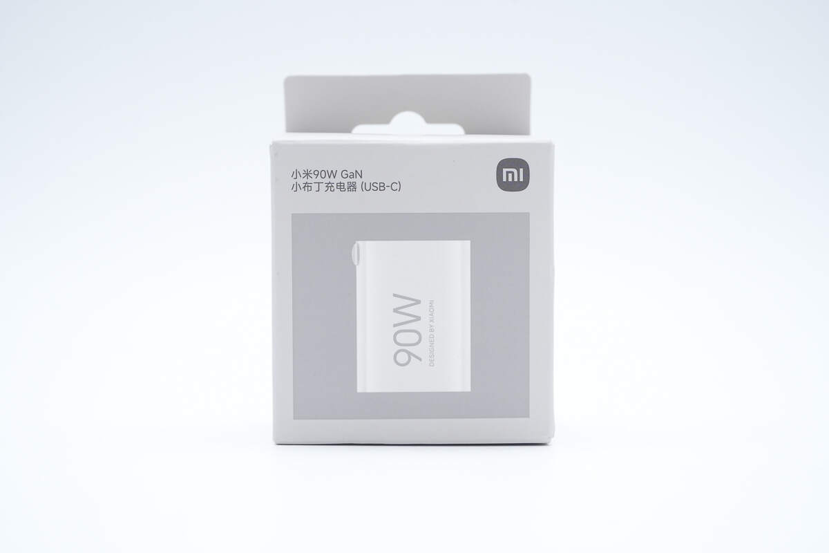
The front of the box features the Xiaomi logo, the product name, and an image of the charger.
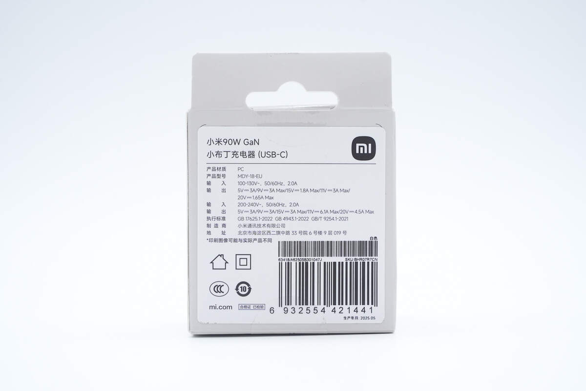
A product information sticker is attached to the back.
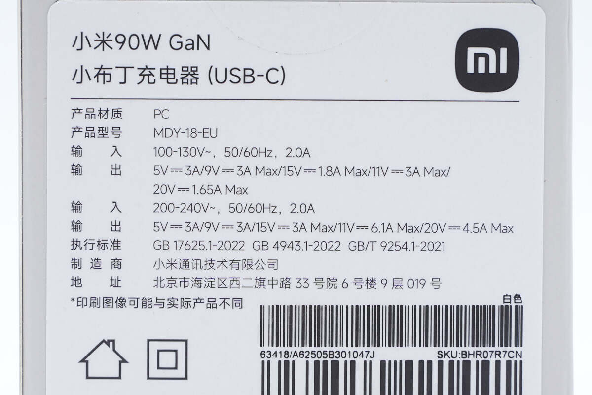
Details will be introduced in the product hands-on display section later.
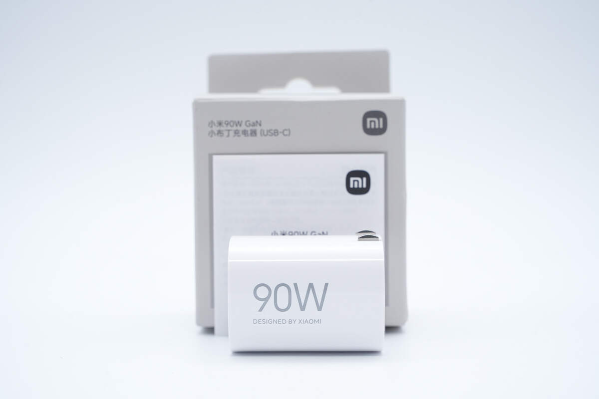
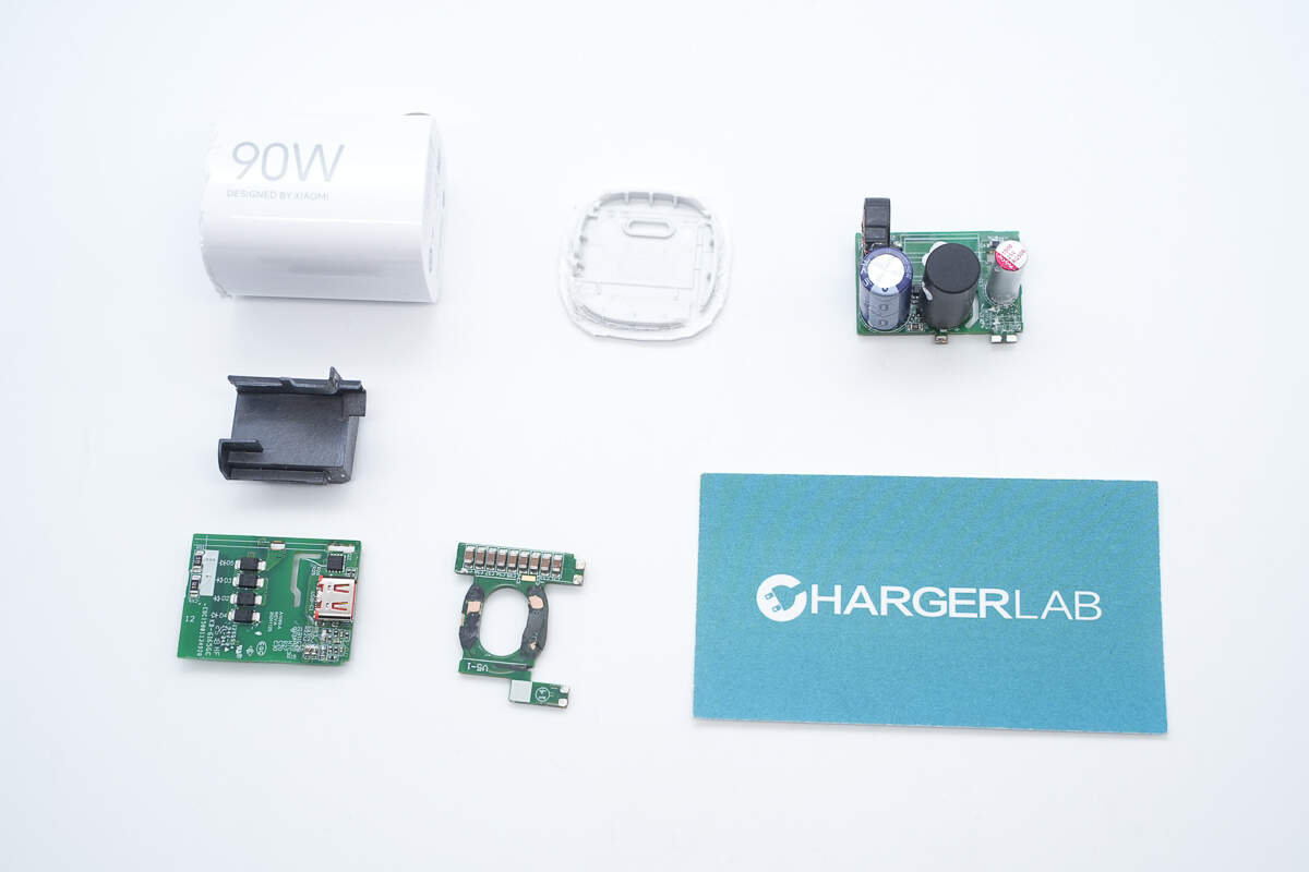
The box contains the charger and some documents.
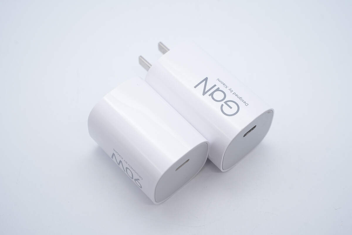
Its surface is smooth with rounded edges.
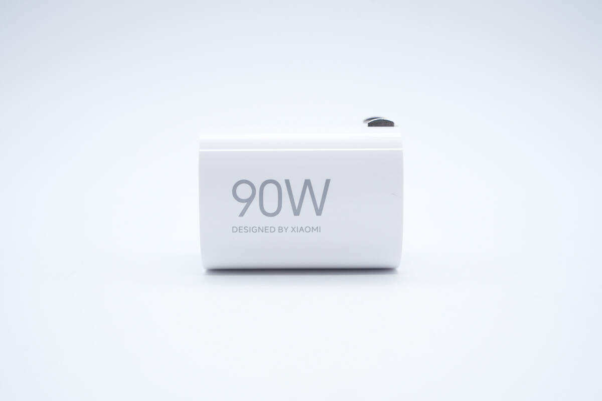
The front is printed with “90W” and “DESIGNED BY XIAOMI.”
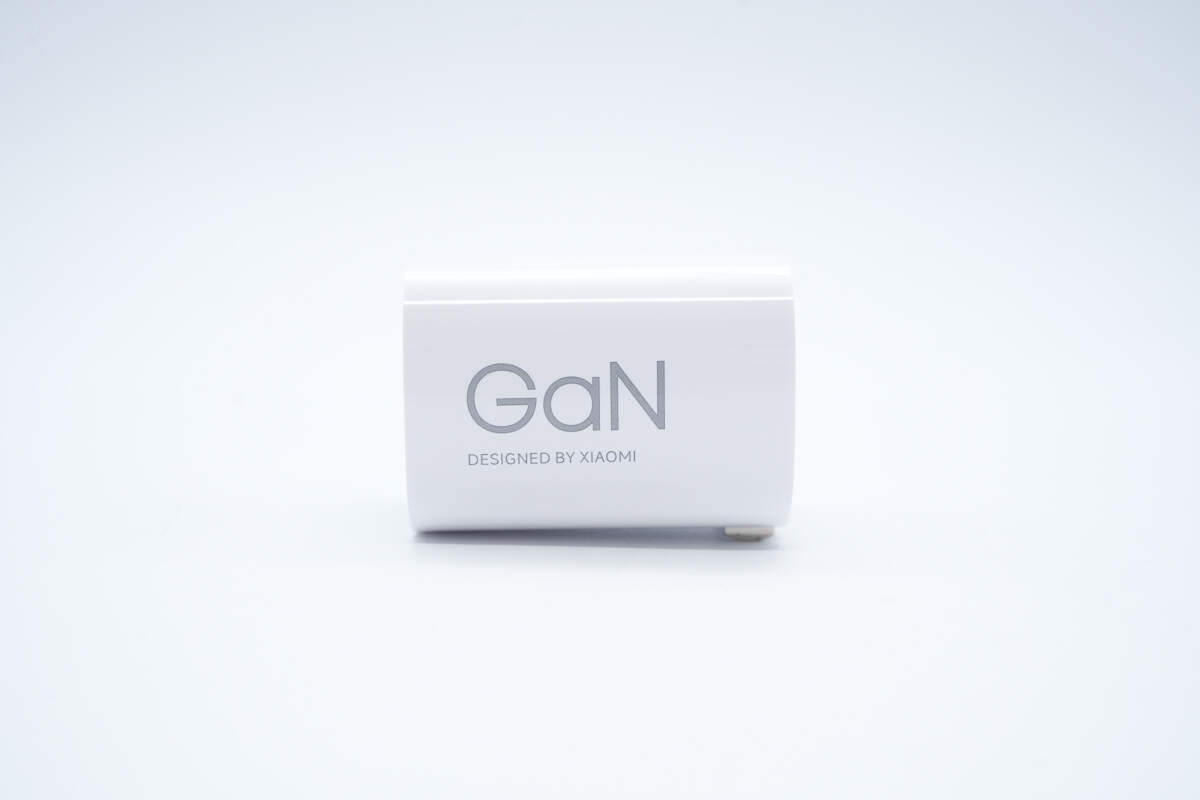
The other side is printed with “GaN” and “DESIGNED BY XIAOMI.”
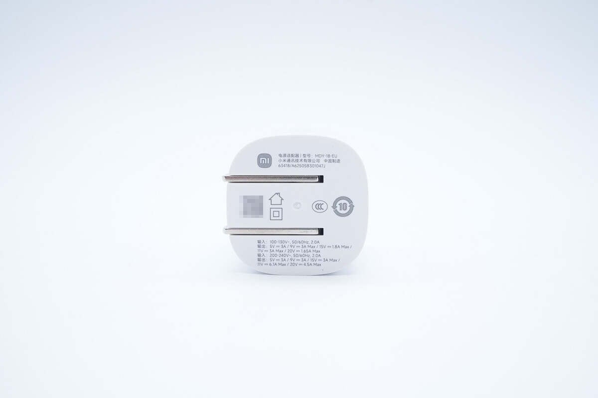
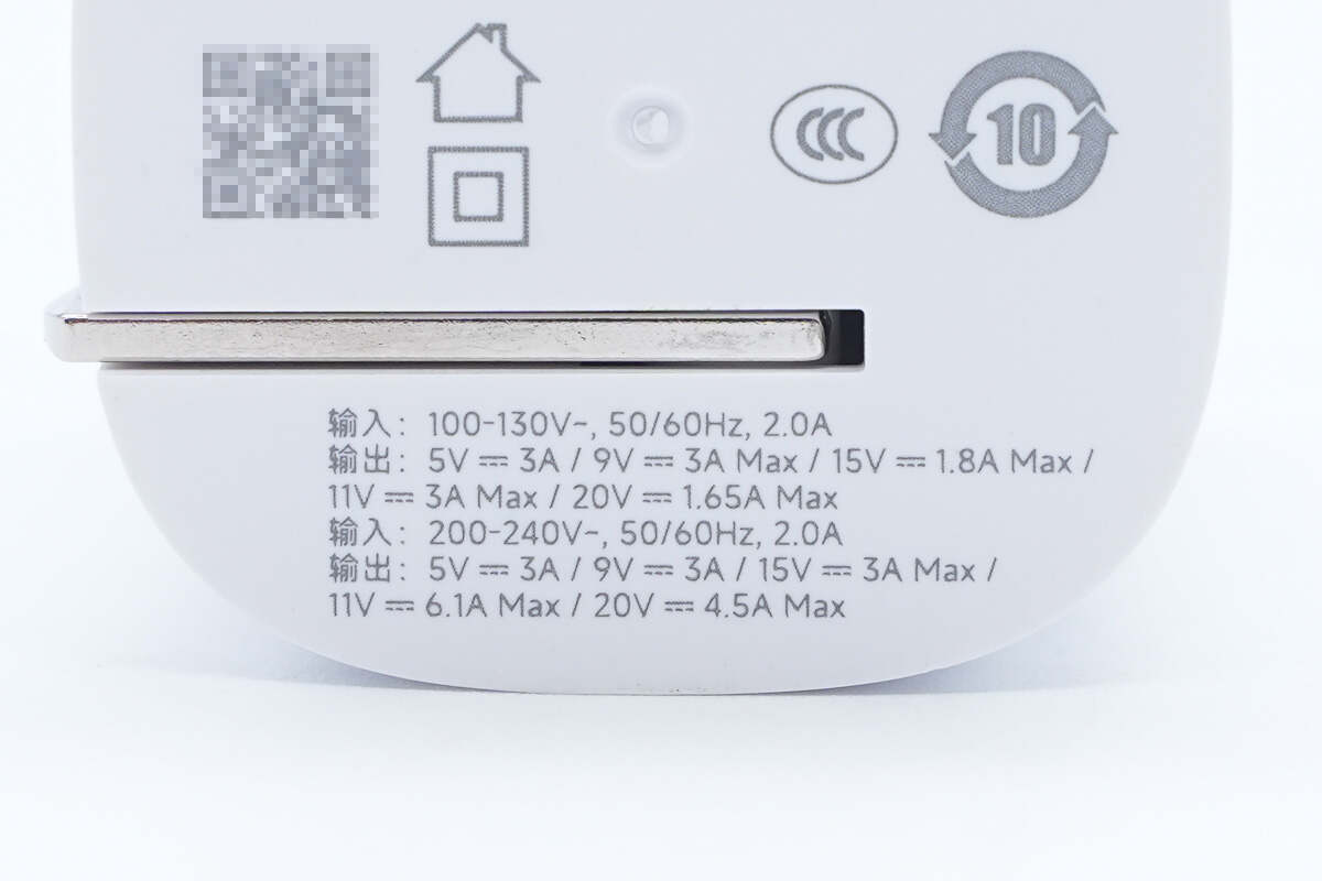
The input side is printed with the specifications.
Model: MDY-18-EU
Input: 100-130V~50/60Hz 2.0A
Output: 5V⎓3A, 9V⎓3A, 15V⎓1.8A, 11V⎓3A, 20V⎓1.65A Max
Input: 200-240V~50/60Hz 2.0A
Output: 5V⎓3A, 9V⎓3A, 15V⎓3A, 11V⎓6.1A, 20V⎓4.5A Max
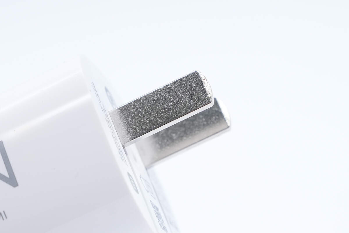
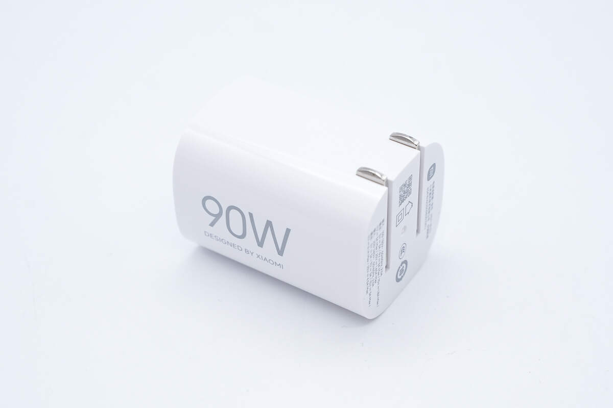
It is equipped with foldable prongs.

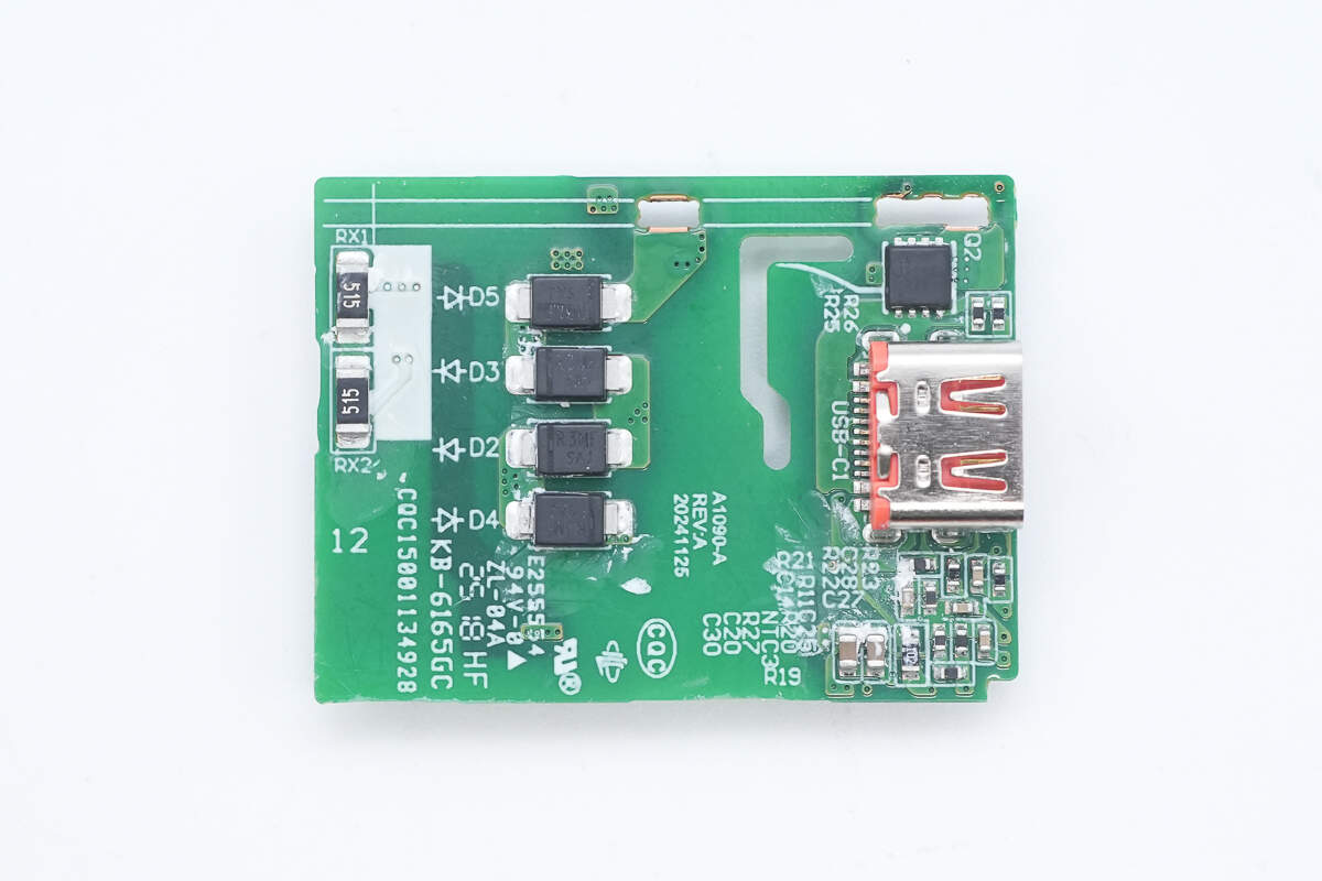
The output end features one USB-C port.
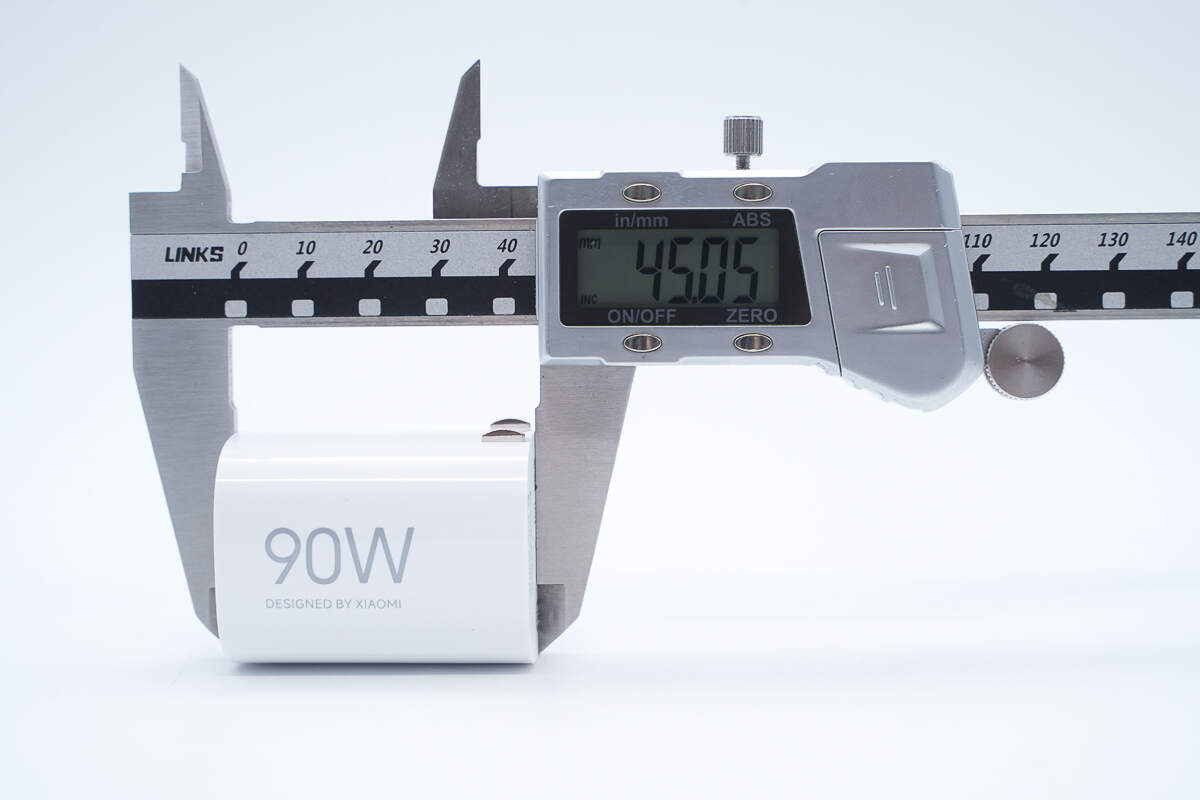
The height is about 45.05 mm (1.77 inches).
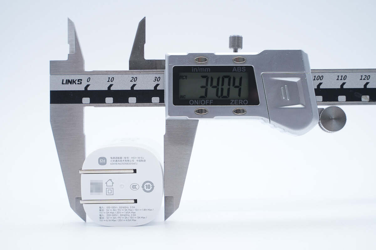
The length is about 34.04 mm (1.34 inches).
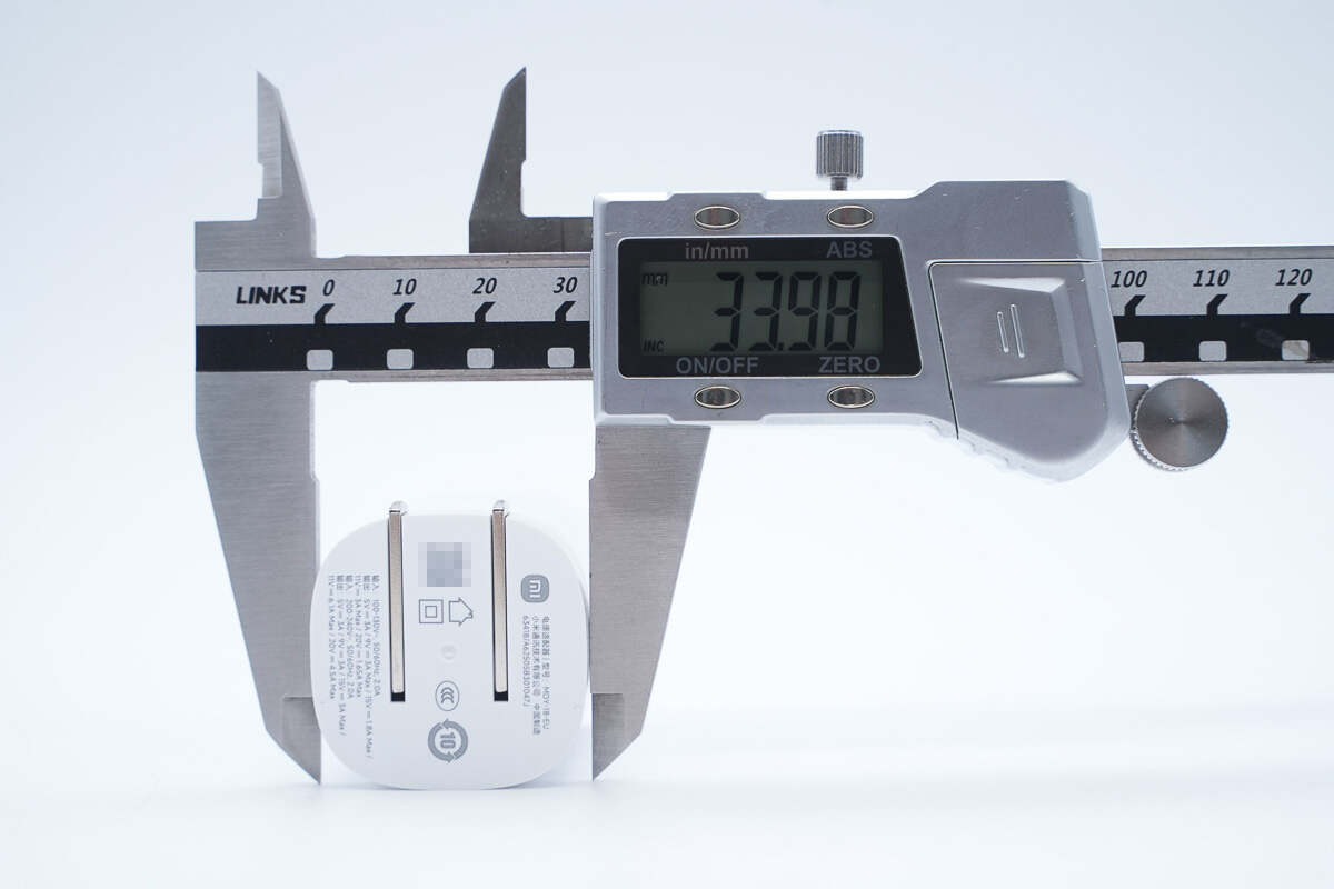
The width is about 33.98 mm (1.34 inches). The volume is about 52.11 cm³. Based on the charger power of 90W, the power density is about 1.73 W/cm³.
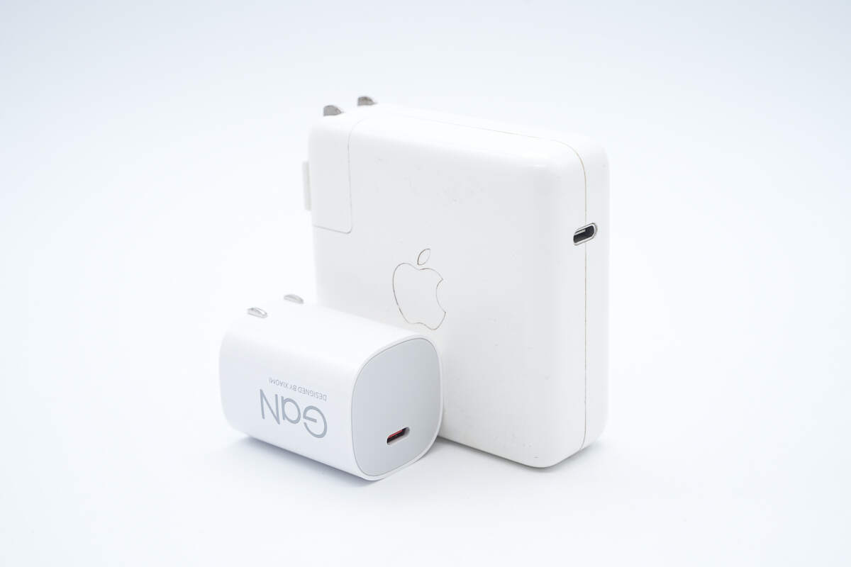
It is significantly smaller than the Apple 87W charger.
Compared to the Xiaomi 120W Pudding charger, this model is slightly shorter in length.
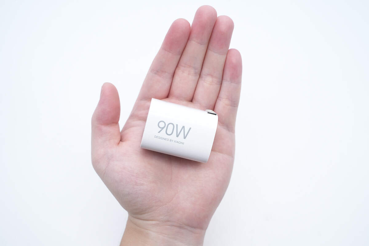
That's how big it is in the hand.
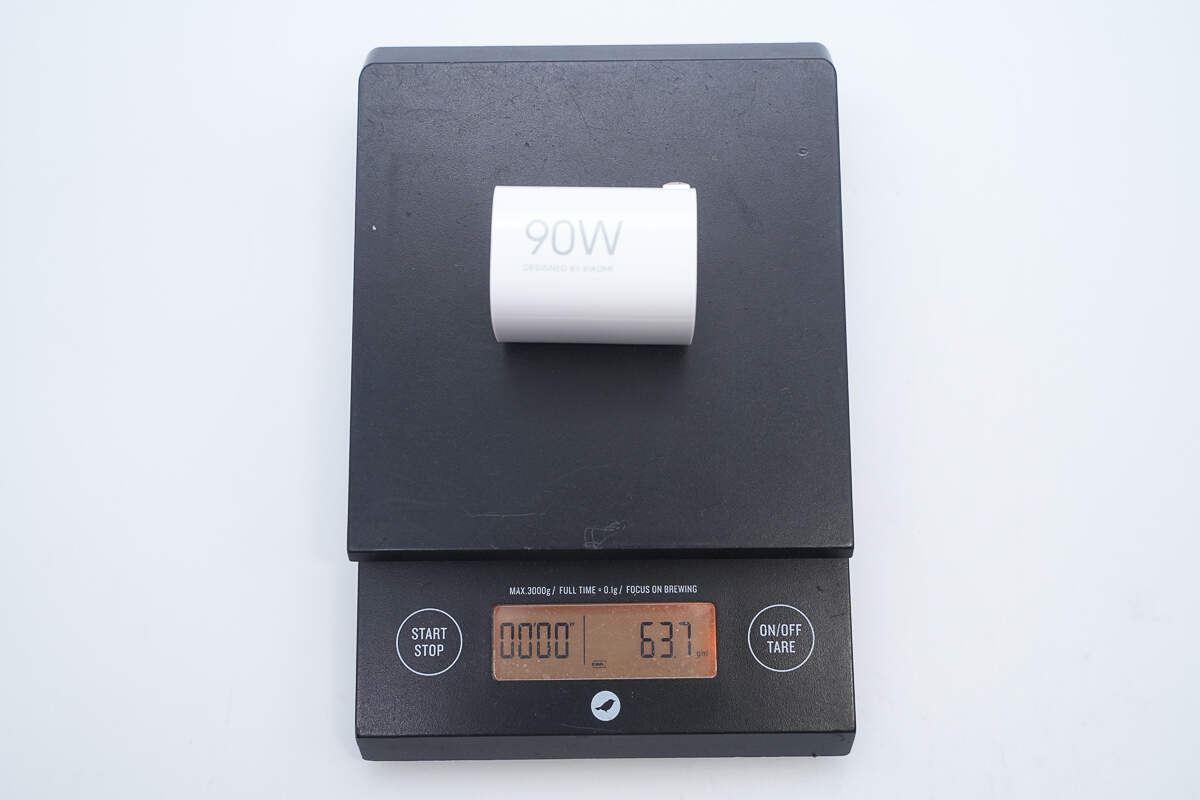
The weight is about 64 g (2.26 oz).
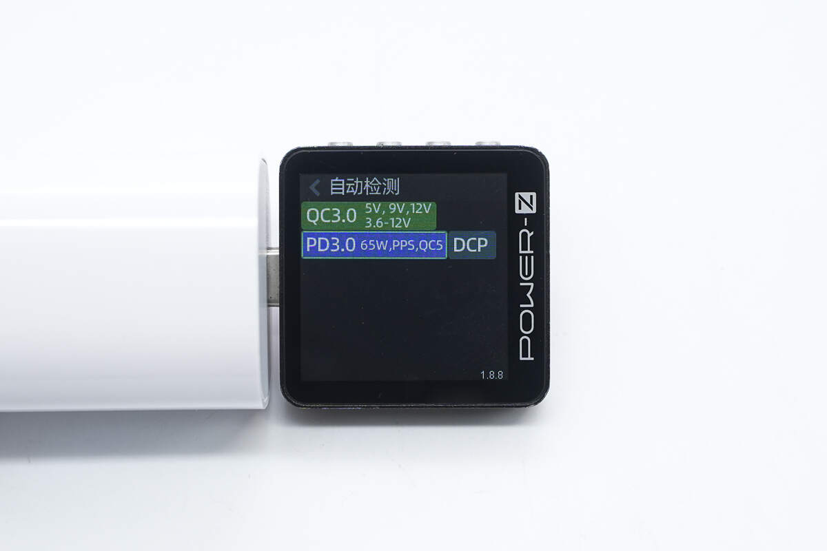
ChargerLAB POWER-Z KM003C shows it supports QC3.0, PD3.0, PPS, and DCP protocols.
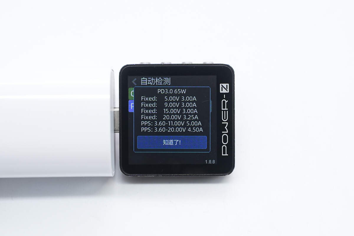
It supports four fixed PDOs of 5V3A, 9V3A, 15V3A, and 20V3.25A, as well as two Xiaomi proprietary fast-charging profiles: 3.6-11V 5A and 3.6-20V 4.5A.
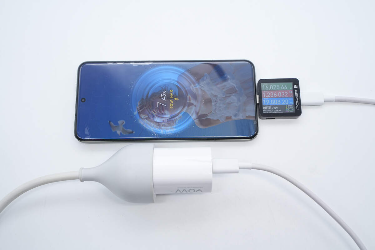
Using it to charge the Xiaomi 15 Pro, the 90W proprietary fast charging was successfully activated.
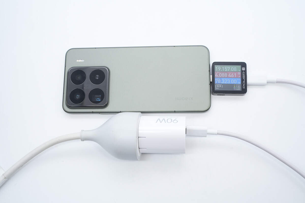
When the charging power climbed to a stable level, the measured power was approximately 78.32W.
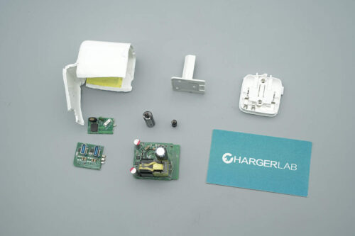
Teardown
Next, let's take it apart to see its internal components and structure.
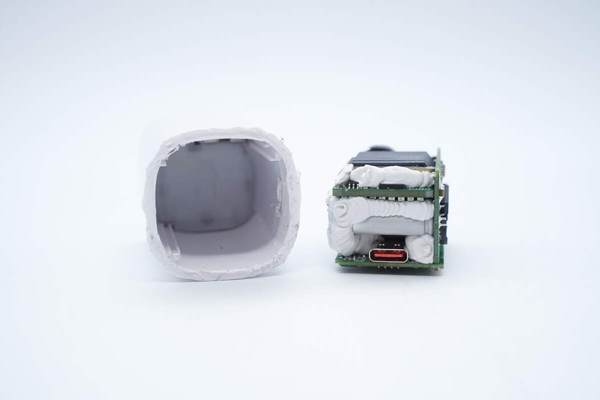
Open the top casing and remove the PCBA module.
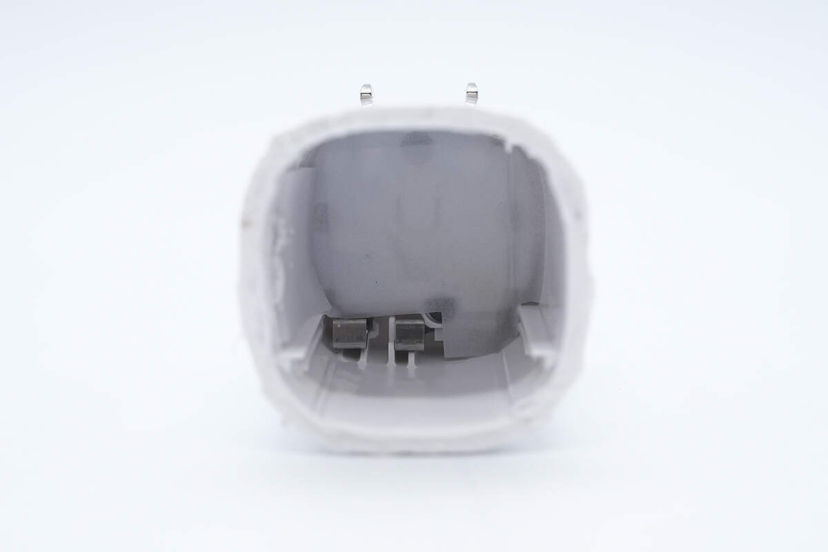
The prongs connect to the PCBA module through metal springs to complete the electrical circuit.
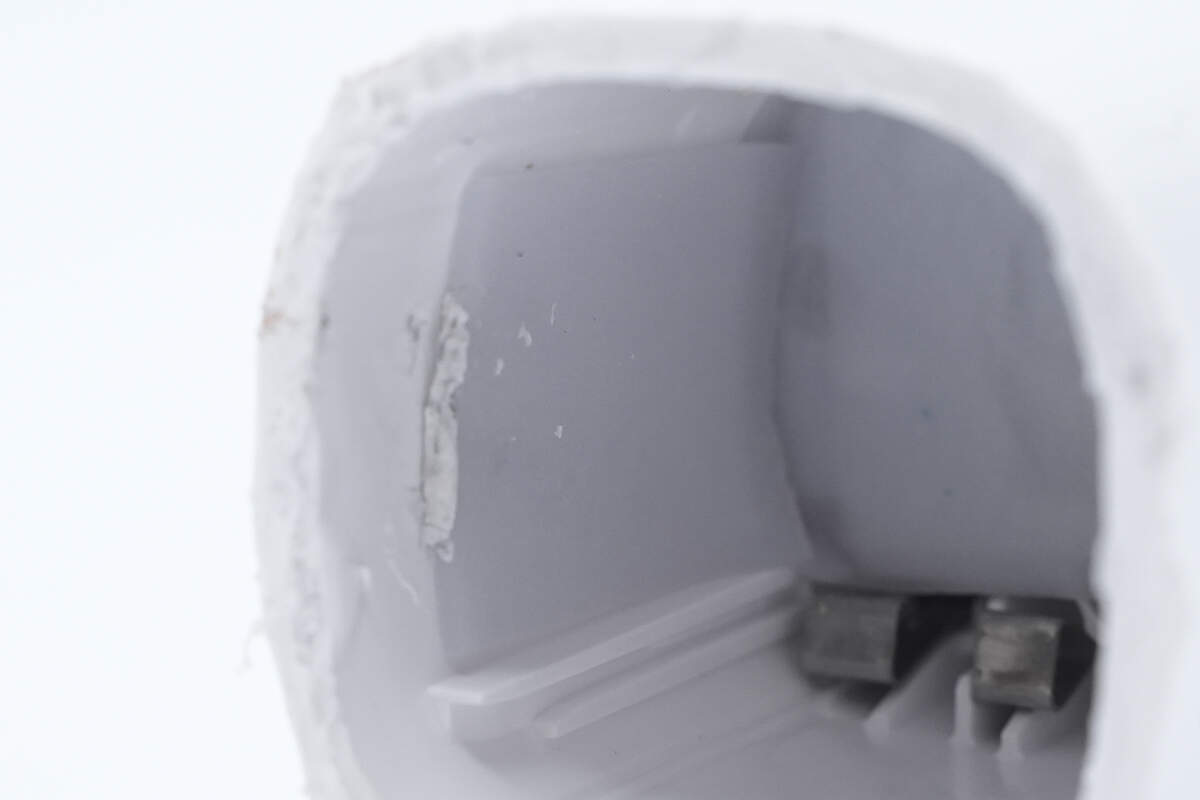
There is a sponge pad attached to the inside of the casing.
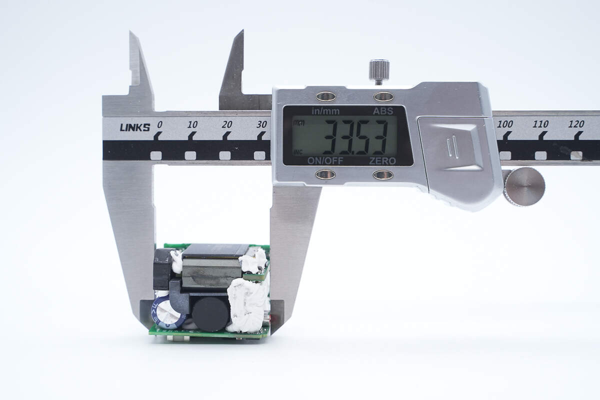
The length of the PCBA module is about 33.53 mm (1.32 inches).
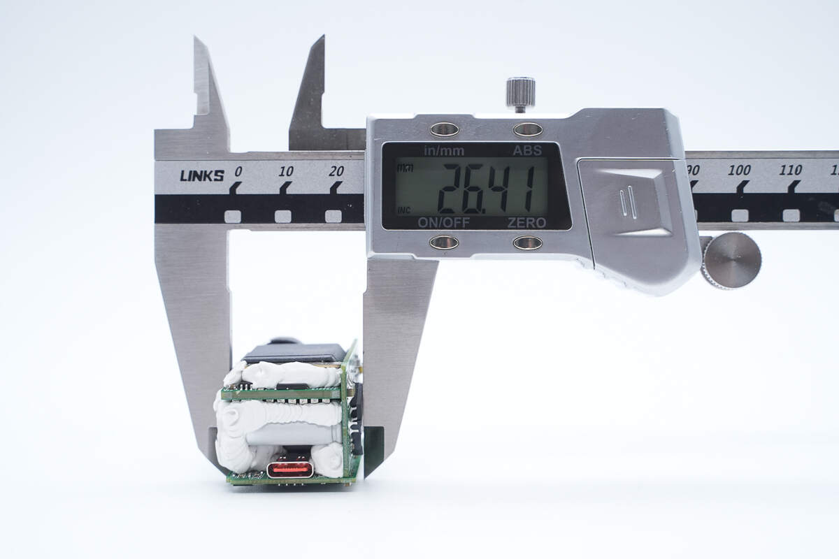
The width is about 26.41 mm (1.04 inches).
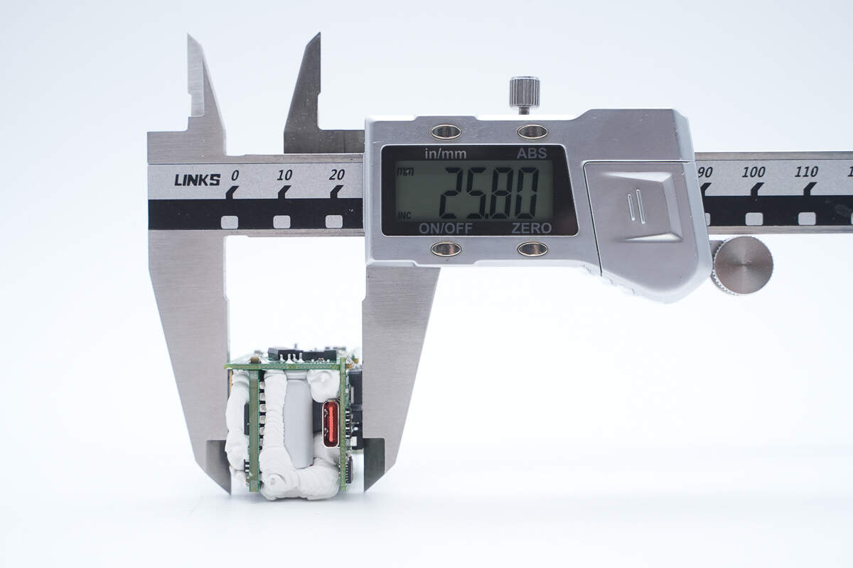
The thickness is about 25.8 mm (1.016 inches).
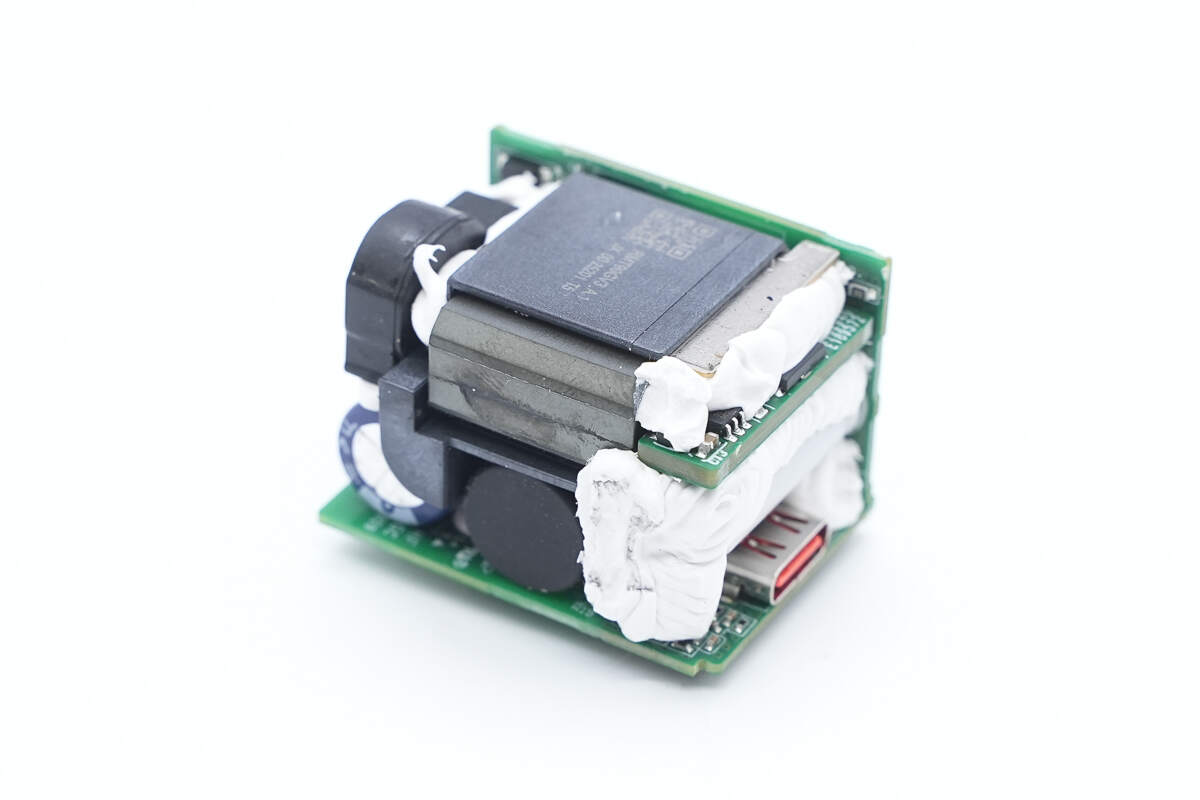
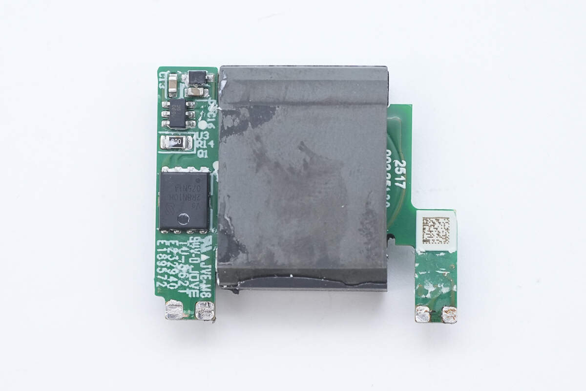
The PCBA module consists of two small PCBs soldered together. There is a planar transformer on the side PCB, and the gap between the PCBs is filled with potting compound for reinforcement.
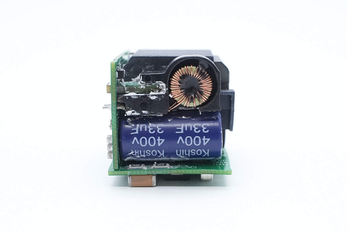
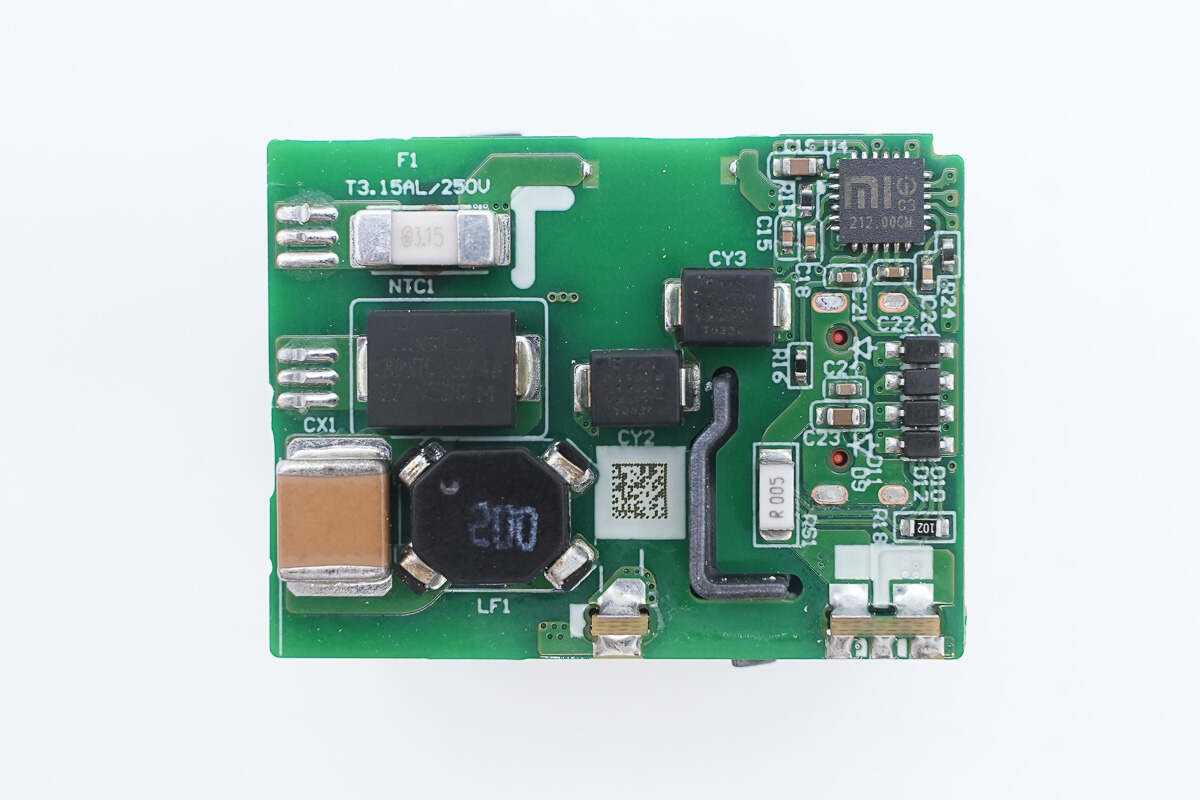
Cleaning off the potting compound, the input end reveals a filter inductor and an electrolytic capacitor.
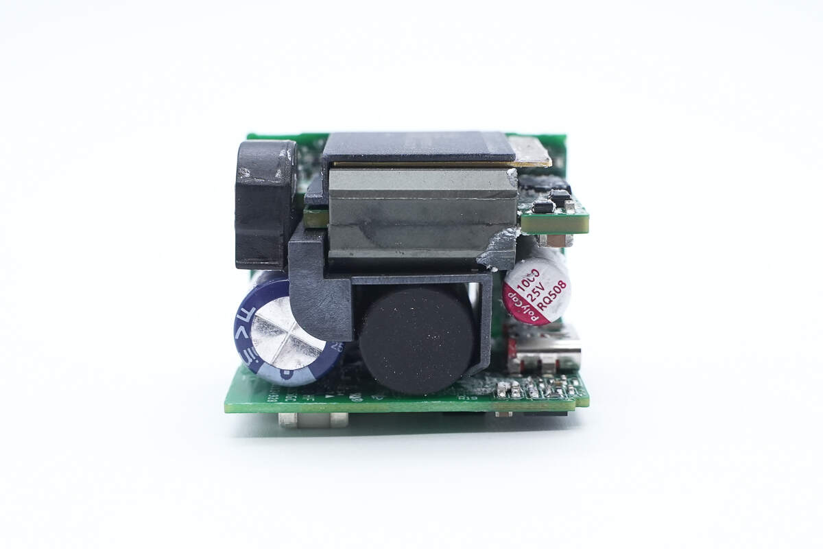
The front of the side PCB is soldered with a planar transformer and a solid capacitor.
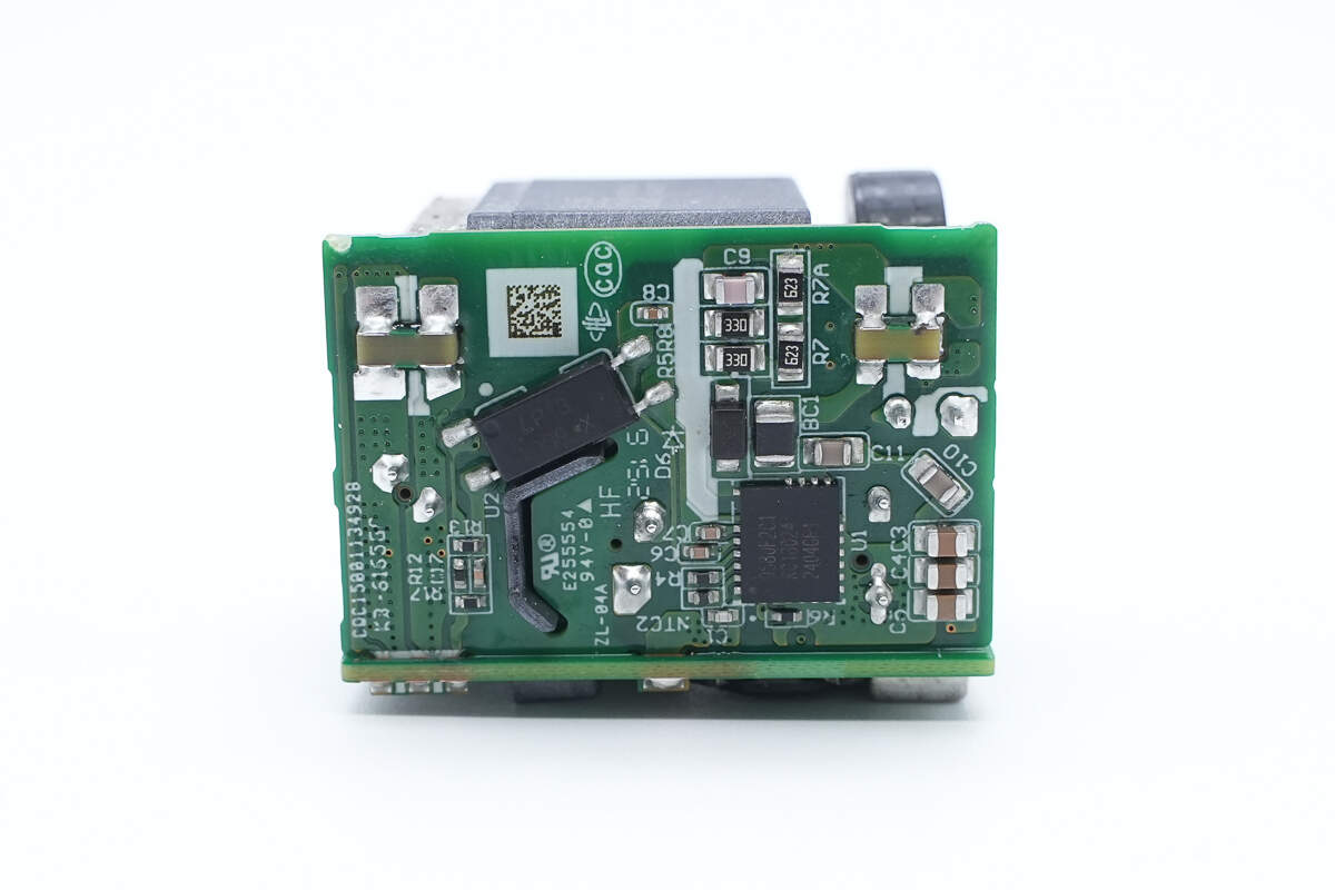
On the back, there is a master control chip and an optocoupler.
The back side of the mainboard is equipped with components such as an SMD fuse, an SMD thermistor, an SMD X capacitor, an SMD common mode choke, an SMD Y capacitor, and a protocol chip.
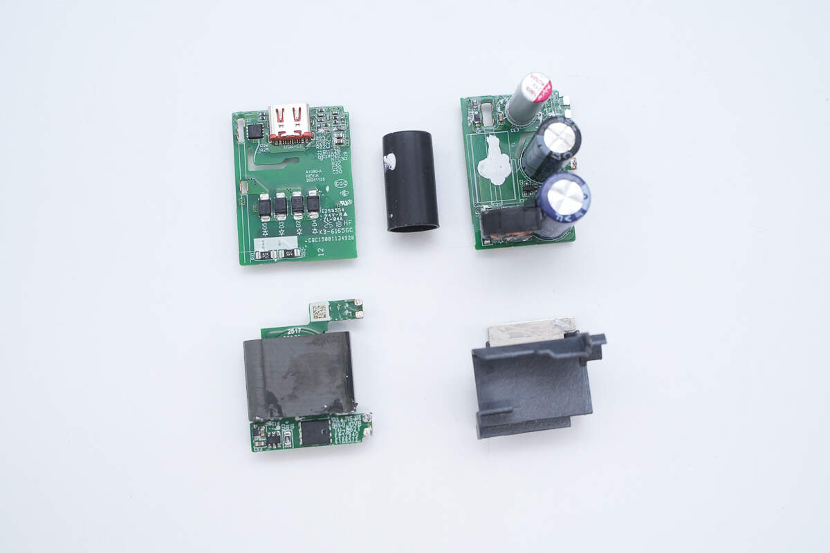
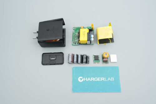
Disassemble the module into separate parts.
The front of the mainboard has four rectifiers and an output VBUS MOSFET.
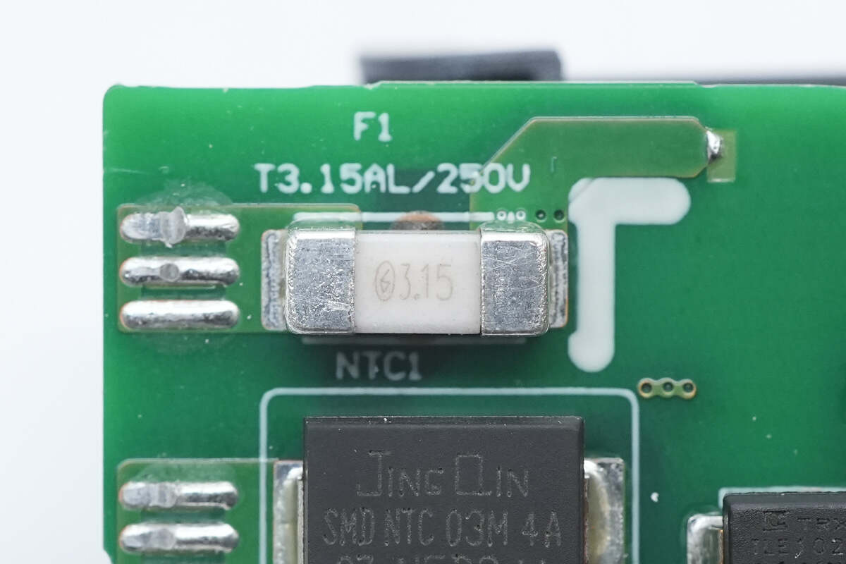
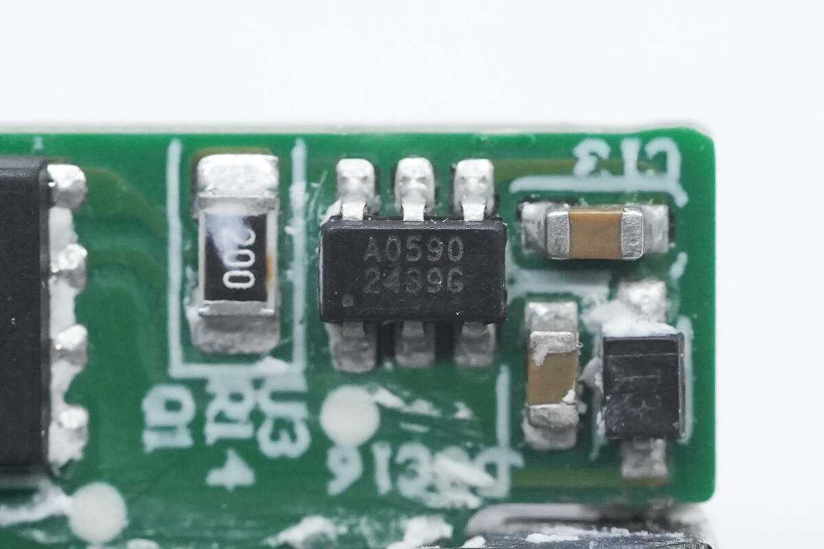
The SMD fuse is rated for a current of 3.15A.
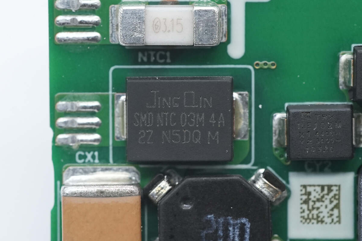
The SMD thermistor is from JinsQin. Model is SMD-NTC03M4A.
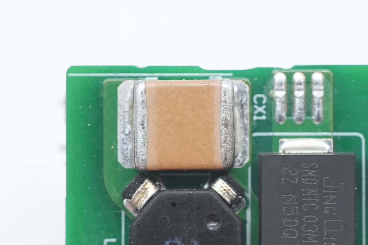
The SMD X capacitor is used to eliminate differential mode interference.
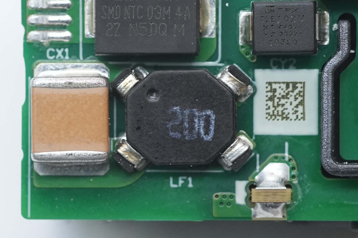
This is the SMD common mode choke.
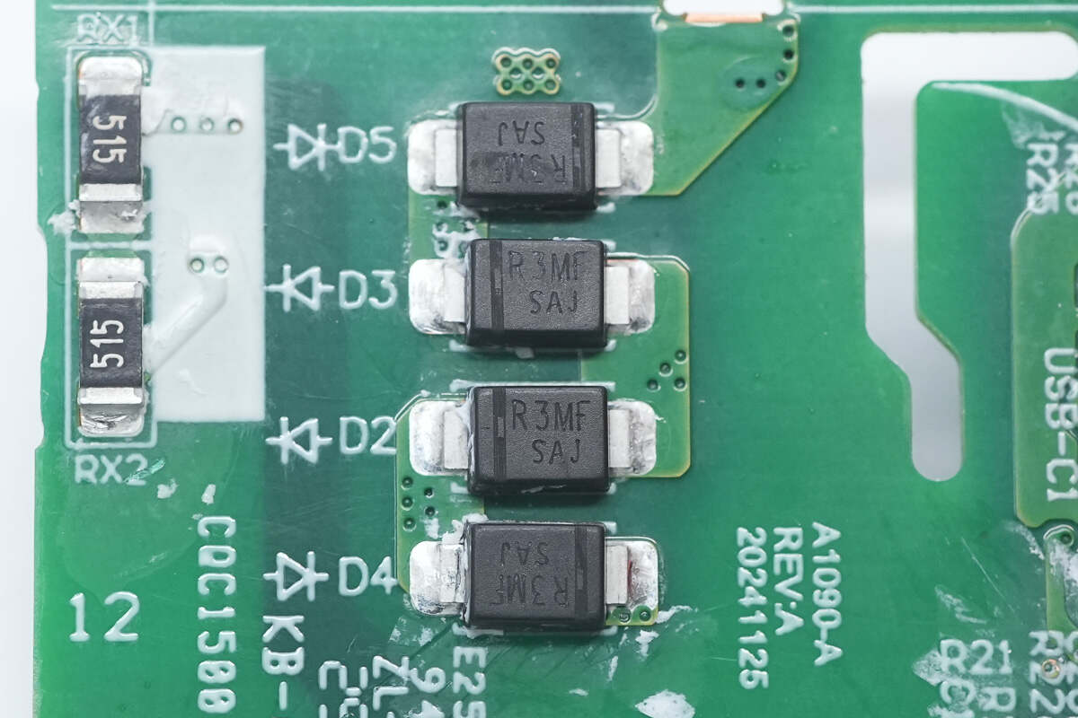
The rectifiers are marked with R3MF and use four units to form a bridge rectifier.
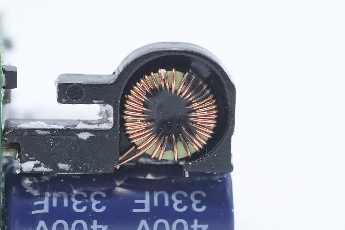
This is the filter inductor.
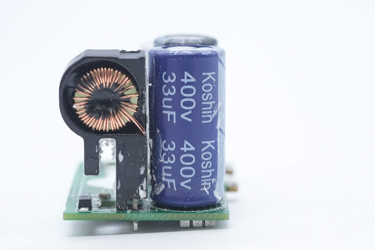
The electrolytic capacitor is from Koshin. 400V 33μF.
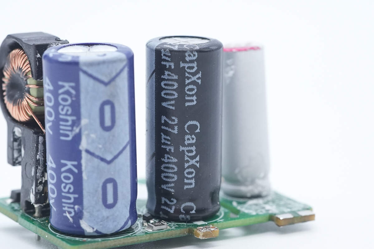
The other electrolytic capacitor is from CapXon. 400V 27μF.
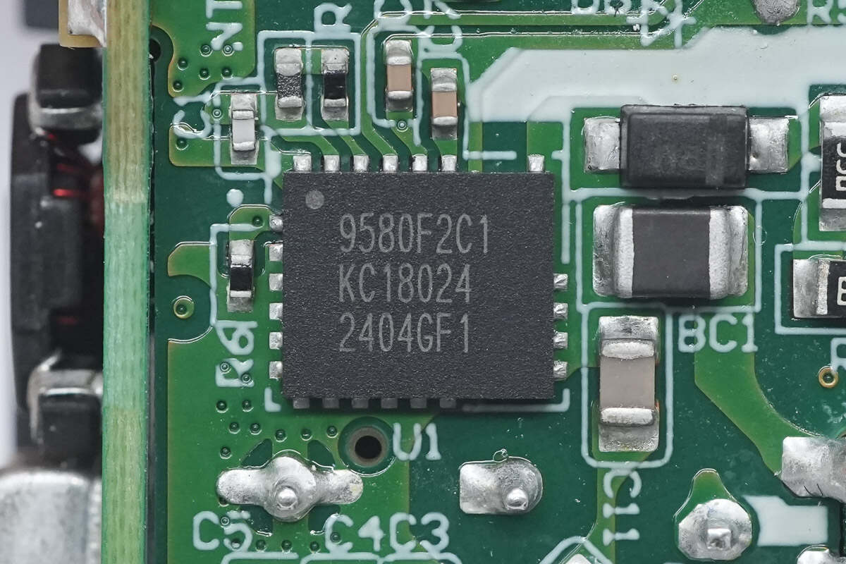
The master control chip is from Navitas' GaNSense Control series. It features a built-in 170mΩ GaN FET and a high-frequency QR controller, offering lossless current sensing, high integration, and high conversion efficiency, enabling compact fast-charging designs. It supports CCM, QR, and DCM control modes and integrates protections such as cycle-by-cycle current limit, AOCP, OTP, and LPS, with an ultra-low standby power consumption of just 20 mW.
The NV9580 comes in a QFN 5x6 package and operates at a maximum switching frequency of 225kHz, helping engineers flexibly design and optimize transformer size and EMI performance. It can operate over a wide VDD range without requiring an additional clamp circuit, reducing BOM costs and shrinking PCB size. Model is NV9580.
The planar transformer is equipped with a synchronous rectifier controller and a synchronous rectifier.
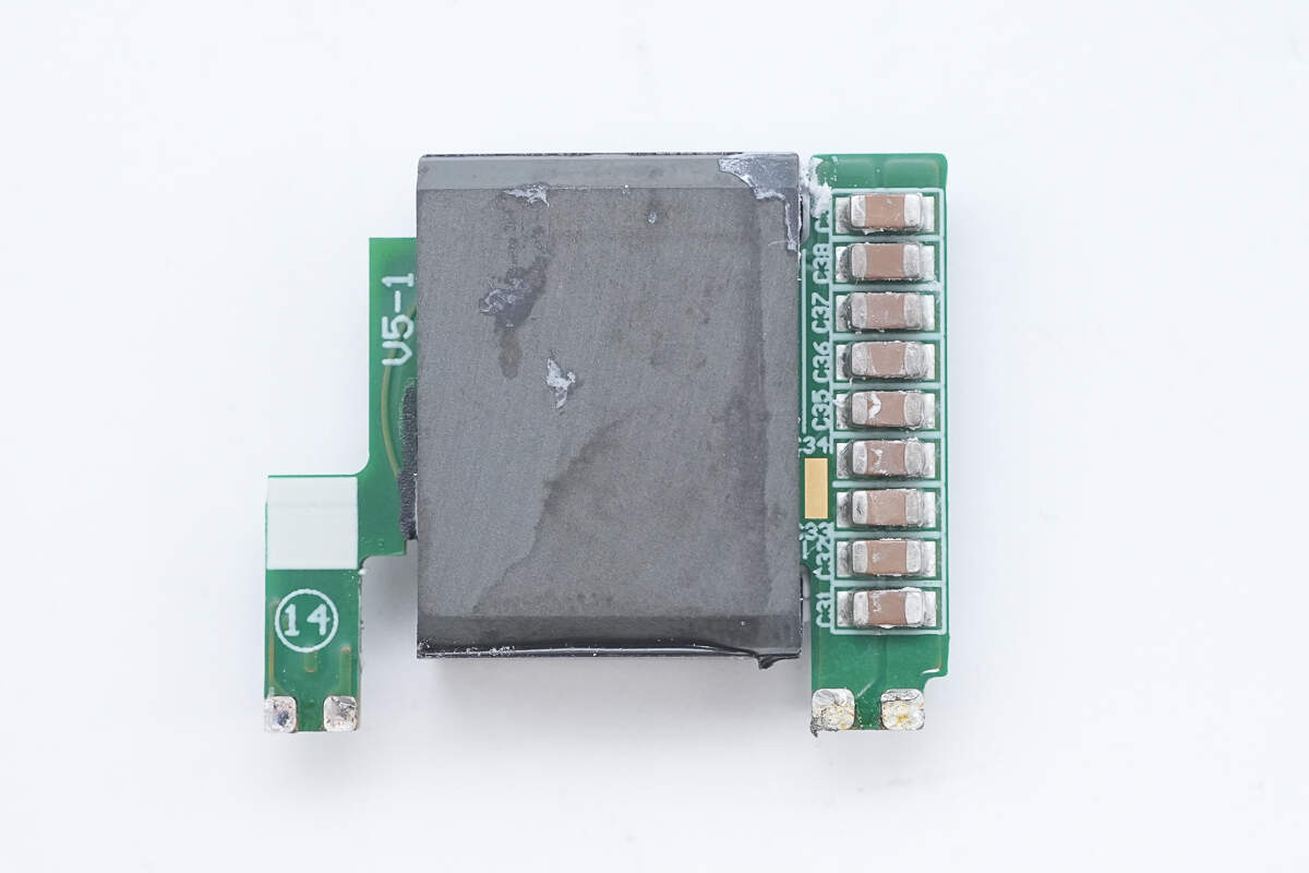
The other side has MLCC filter capacitors.
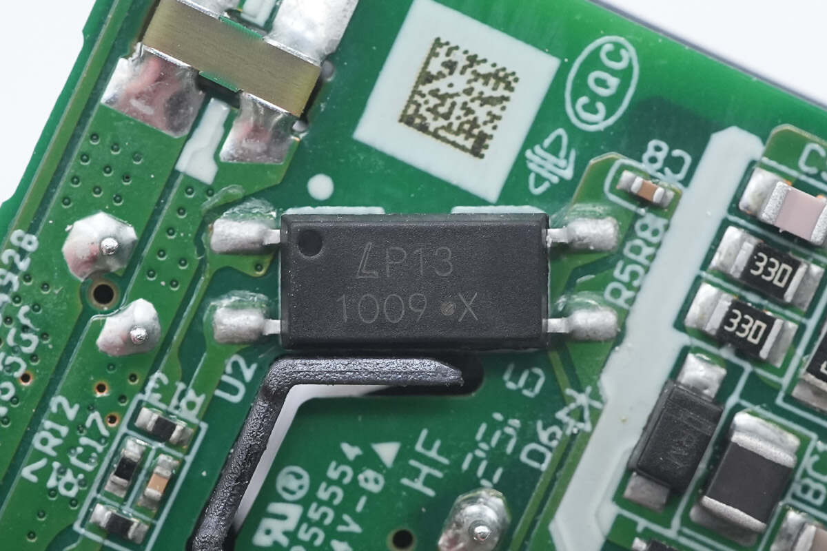
The 1009 optocoupler is used for output voltage feedback.
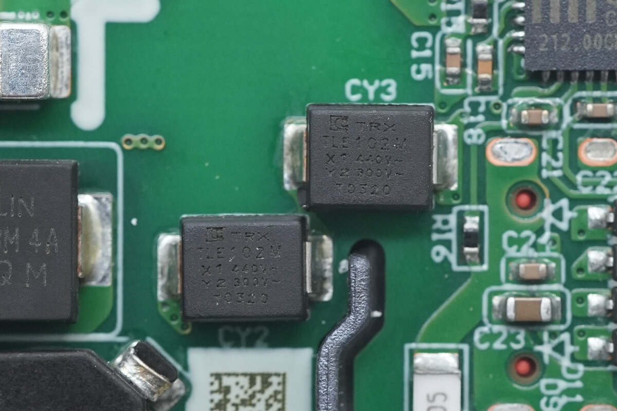
The SMD Y capacitor is from TRX. Its small size and light weight are suitable for high-density power products such as GaN fast chargers.
The synchronous rectifier controller is also from Navitas and adopts the SOT-23-6L package. It uses a patented shut-off control algorithm, enabling stable support for DCM, QR, and CCM modes, which helps achieve a highly reliable flyback converter design. Model is NV9701.
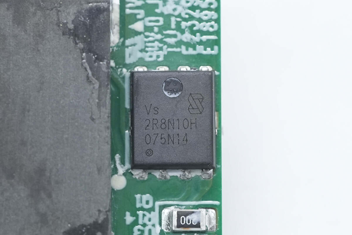
The synchronous rectifier is from Vergiga and adopts the PDFN5060X package. Model is VSP2R8N10HS-G. 100V 2.3mΩ.
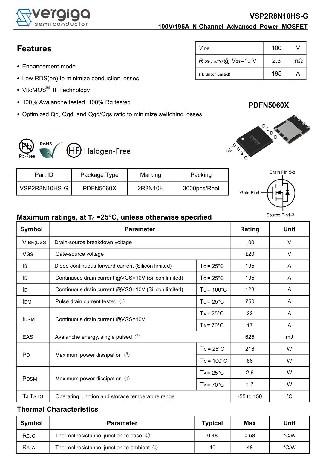
This is the information about Vergiga VSP2R8N10HS-G.
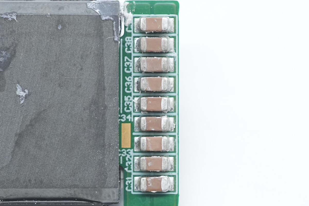
There are MLCC filter capacitors.
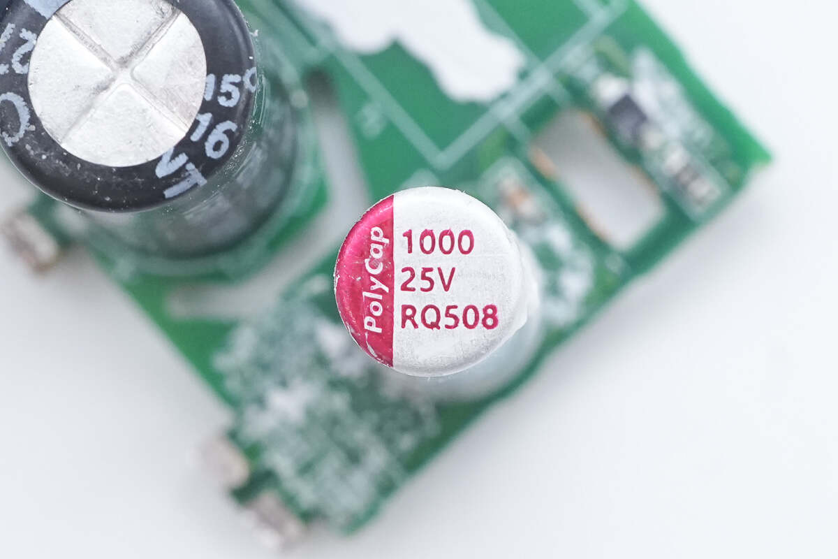
The solid capacitor for output filtering is from PolyCap. 25V 1000μF.
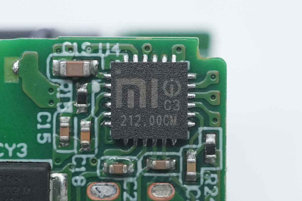
The protocol chip is custom-made by Injoinic for Xiaomi. The chip is marked with both Xiaomi’s and Injoinic’s logos, as well as C3.
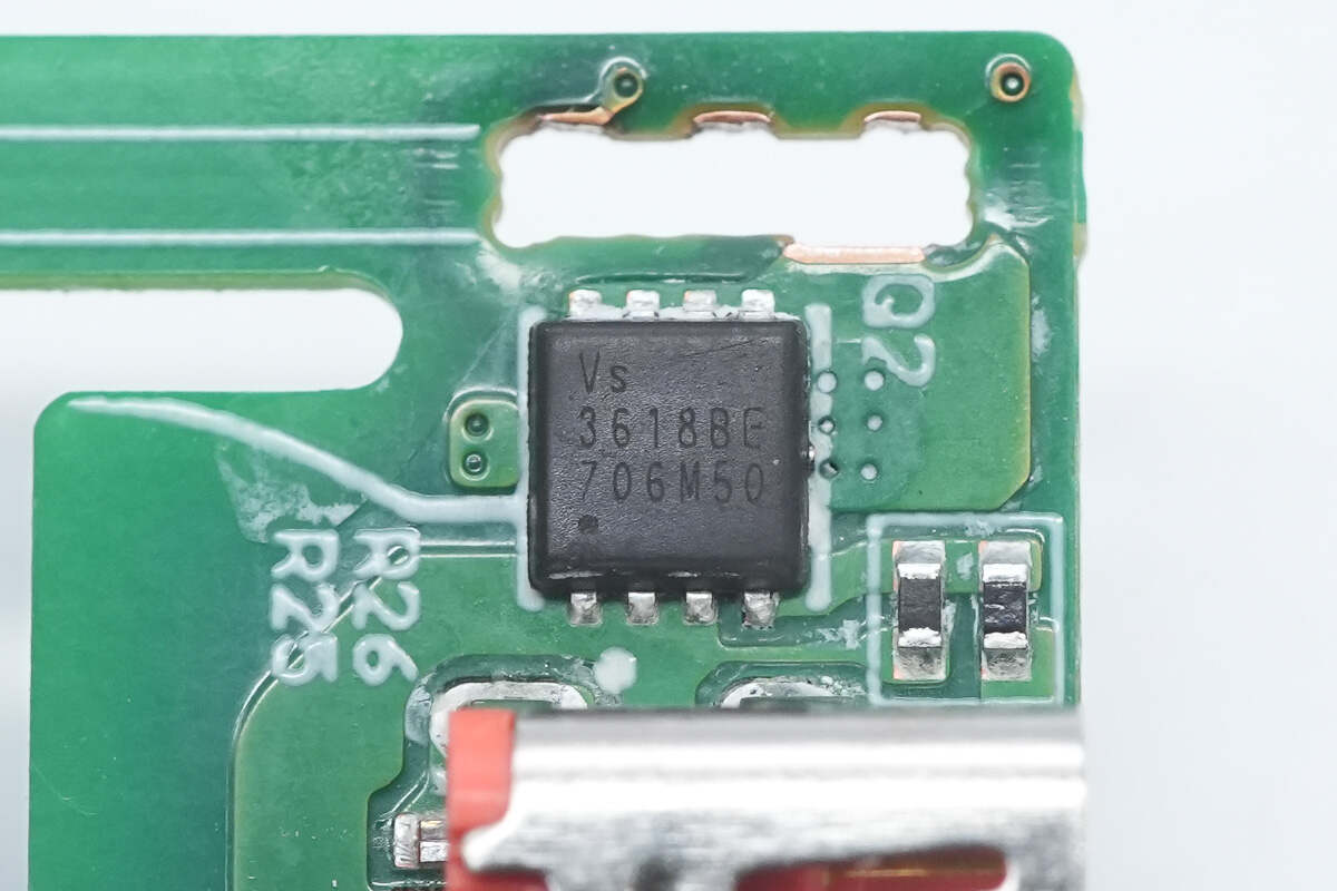
The VBUS MOSFET is from Vergiga and adopts the PDFN3333 package. 30V 5.2mΩ. Model is VS3618BE.
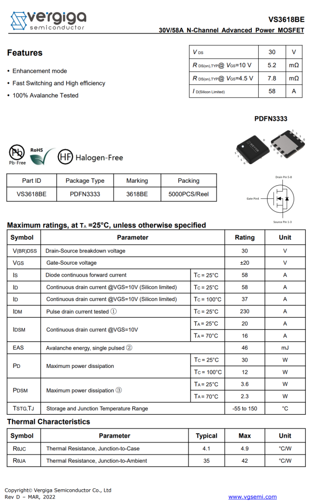
There is information about Vergiga VS3618BE.
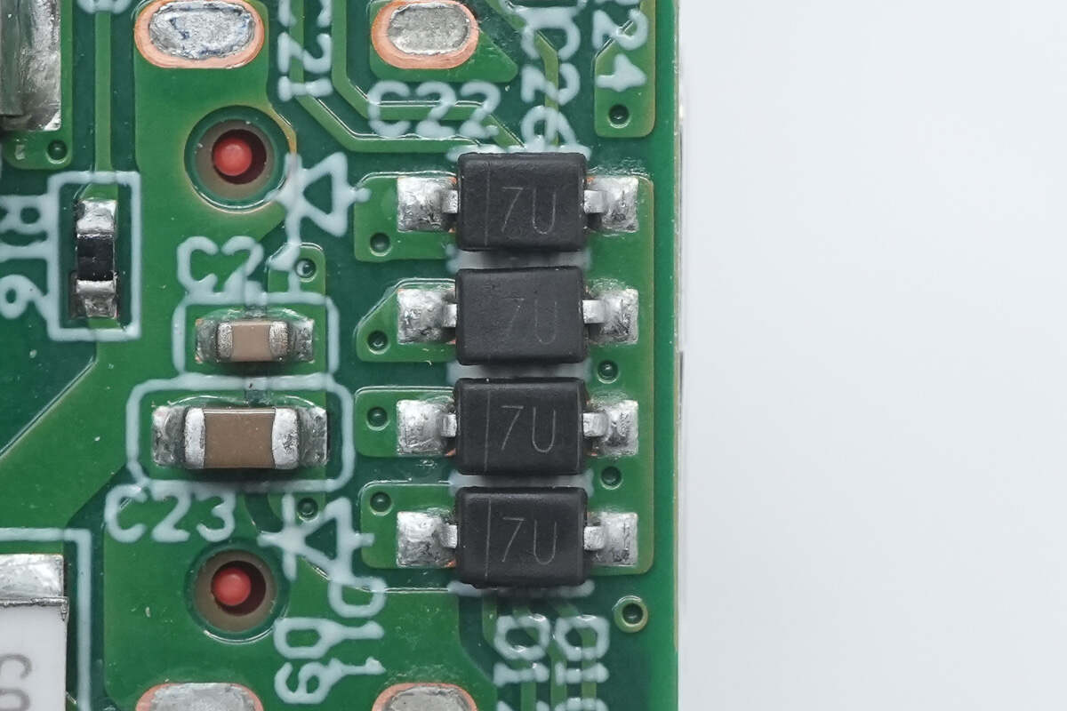
The TVS marked with 7U is used for overvoltage protection at the port end.
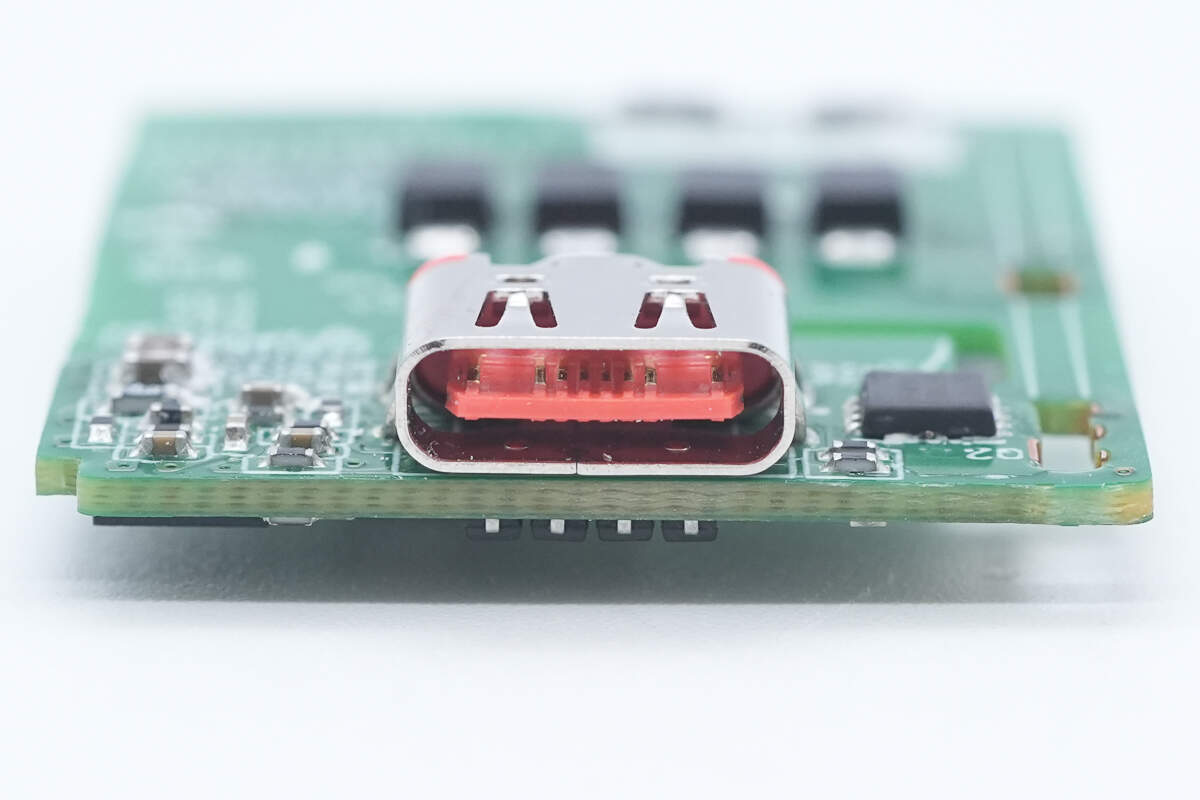
There is the USB-C socket.
Well, those are all components of the Xiaomi 90W GaN Pudding Charger.
Summary of ChargerLAB
Here is the component list of the Xiaomi 90W GaN Pudding Charger for your convenience.
The Xiaomi 90W Pudding charger continues the series’ design language with a compact, smooth, and uniquely styled body. Equipped with foldable prongs, it offers enhanced portability and convenience. It supports Xiaomi proprietary 90W fast charging protocol as well as 65W PD fast charging, not only meeting the fast-charging needs of devices like the Xiaomi 15 Pro but also powering laptops and other equipment.
After taking it apart, we found that it is designed based on Navitas Semiconductor’s highly integrated GaN solution, combining the NV9580 and NV9701 chips. It uses MOSFETs from Vergiga
and a custom protocol chip from Injoinic to control output. The PCBA module employs a modular planar transformer stacked with two additional small PCBs. Together with the GaN design, this not only keeps the overall size very compact but also ensures stability and efficient heat dissipation.
Related Articles:
1. Teardown of Huawei Pura X Original 66W GaN Charger (HW-110600C05)
2. Teardown of ANKER 253W GaN Power Adapter
3. Teardown of ANKER 150W 4 USB-C Ports GaN Charger