Introduction
The VERYSUN 100W GaN Charger X100Pro features two USB-C ports and one USB-A port. Despite its compact design, it includes a TFT smart display that provides real-time power readings and temperature monitoring.
Both USB-C ports support 100W output and are compatible with PD3.2. With PPS fast charging capabilities, the charger offers a voltage range of 9-20V at 5A. Next, through a detailed teardown, we will take a closer look at its internal design and component selection.
Product Appearance
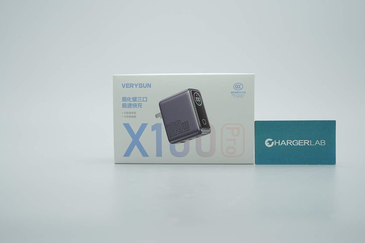
The front of the packaging box features the VERYSUN logo, product name, appearance, and model number.
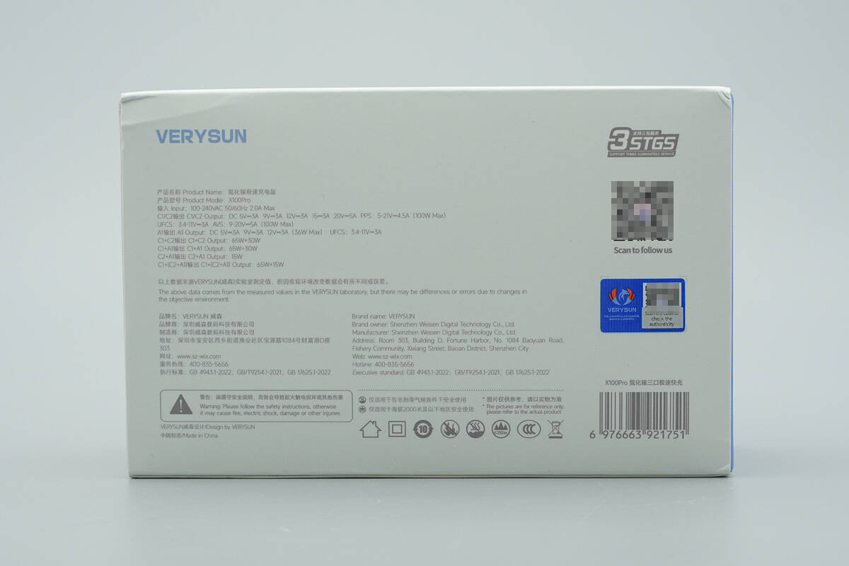
The back of the packaging displays product specifications, as well as merchant information and other relevant details.
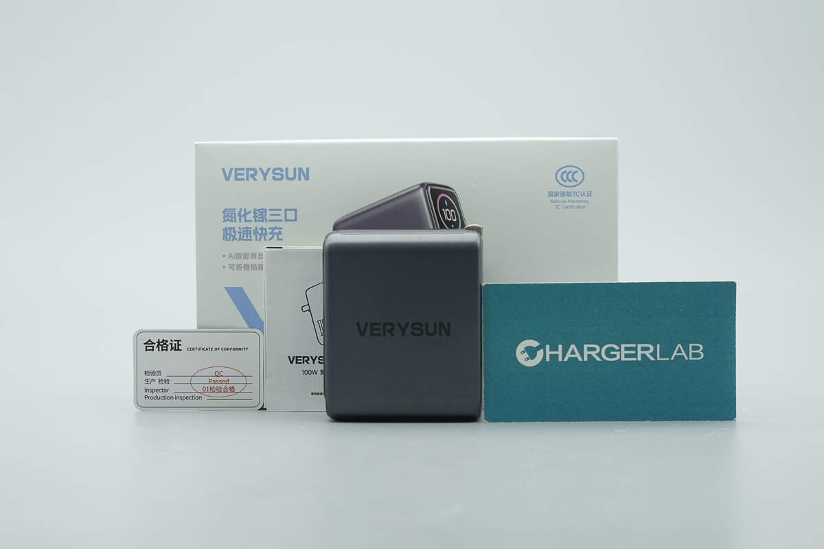
The package includes the charger, user manual, and a certificate of conformity.
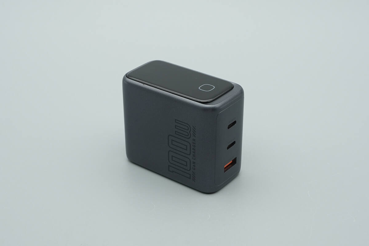
The outer shell is made of PC flame-retardant material with a painted surface finish.
The center of the front is printed with the VERYSUN logo.
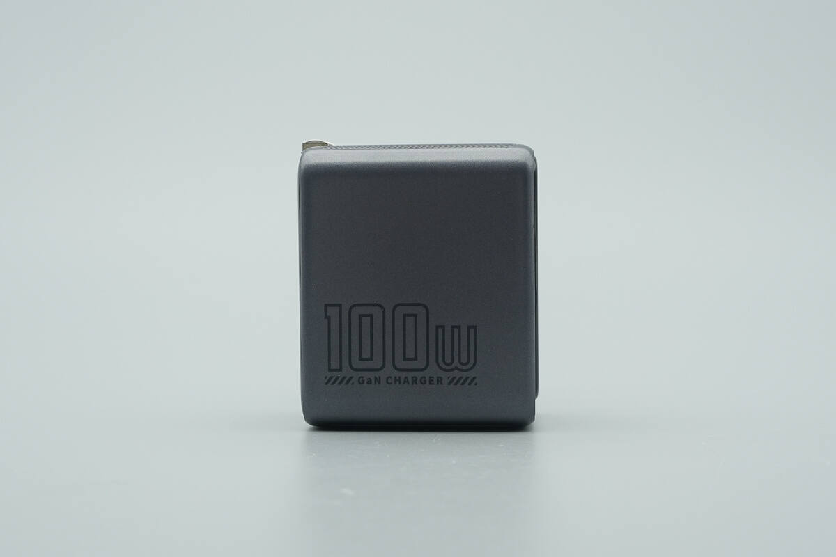
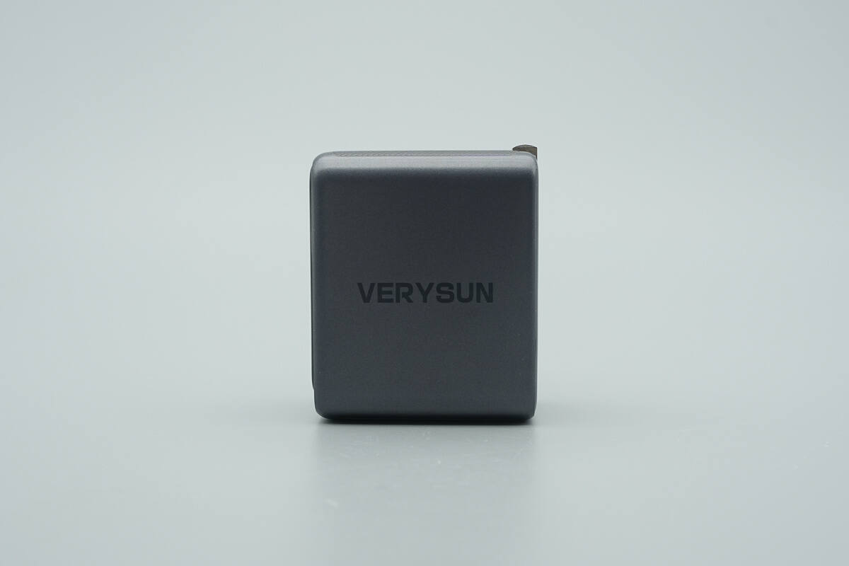
The back of the charger is printed with "100W GaN CHARGER."
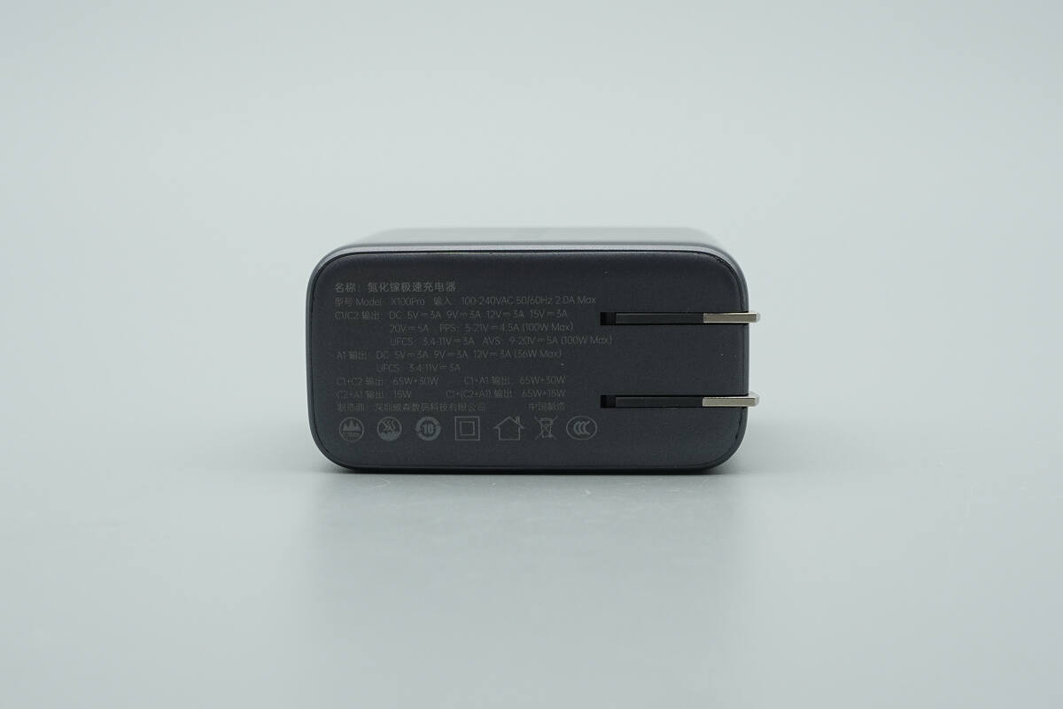
The bottom of the shell is printed with the parameter information.
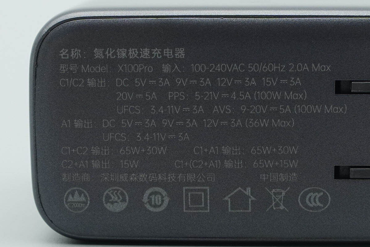
Model: X100Pro
Input: 100-240V~50/60Hz 2A Max
C1/C2 Output: DC 5V3A, 9V3A, 12V3A, 15V3A, 20V5A
PPS: 5-21V-4.5A (100W Max)
UFCS: 3.4-11V3A
AVS: 9-20V5A (100W Max)
A1 Output: DC 5V3A, 9V3A, 12V3A (36W Max)
UFCS: 3.4-11V3A
C1 + C2: 65W + 30W
C1 + A1: 65W + 30W
C2 + A1: 15W
C1 + (C2 + A1): 65W + 15W
The product has passed CCC certification.
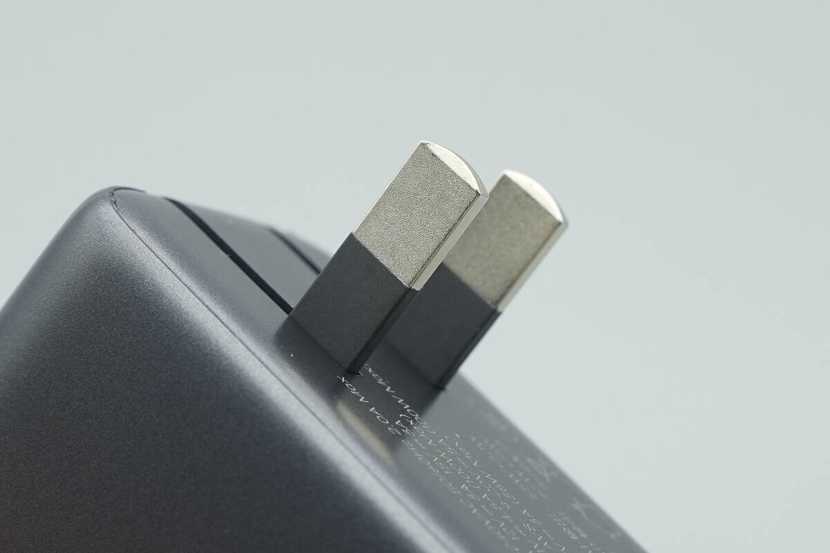
It is equipped with foldable plugs.
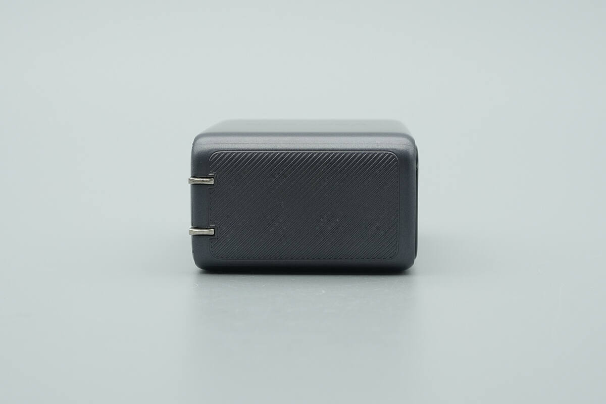
This side has a diagonal texture.
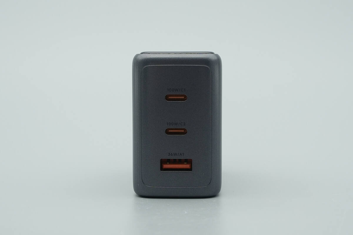
The other end is equipped with two USB-C ports and one USB-A port.
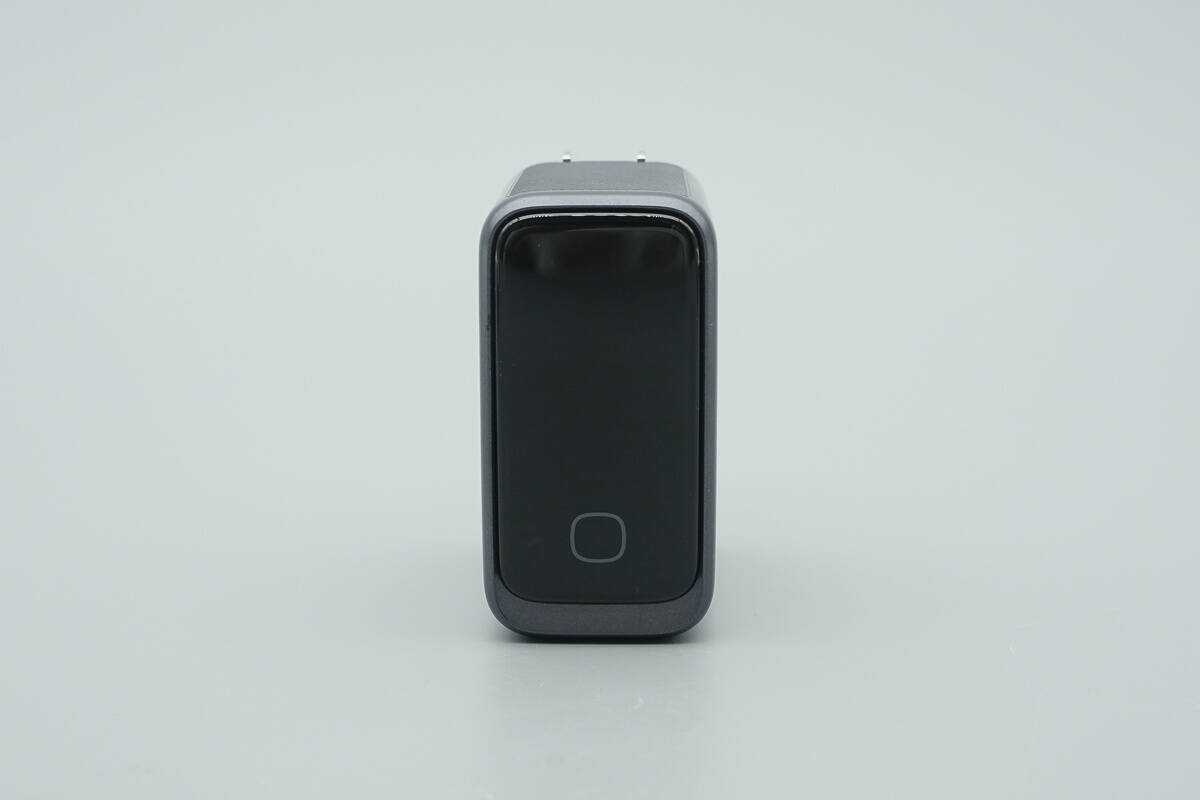
The top is equipped with a TFT smart display and touch control buttons.
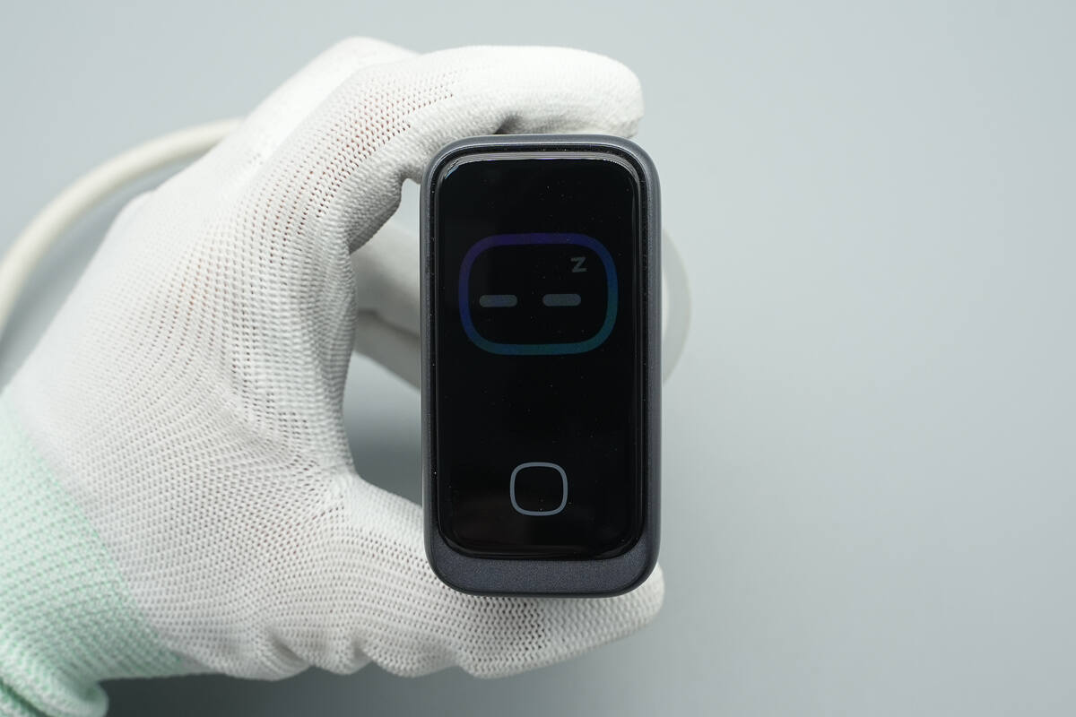
When powered on, the screen lights up with interactive standby expressions.
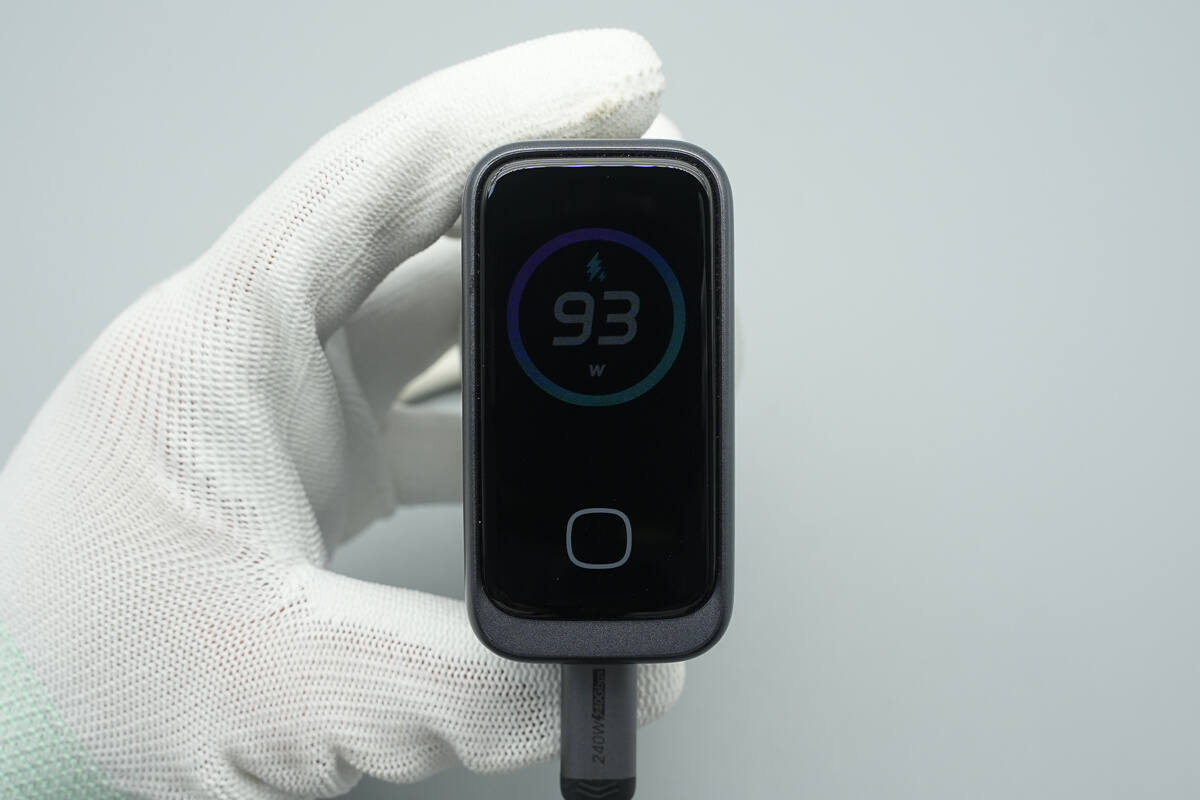
The interface can be switched through the touch control buttons, and the screen displays the total output power.
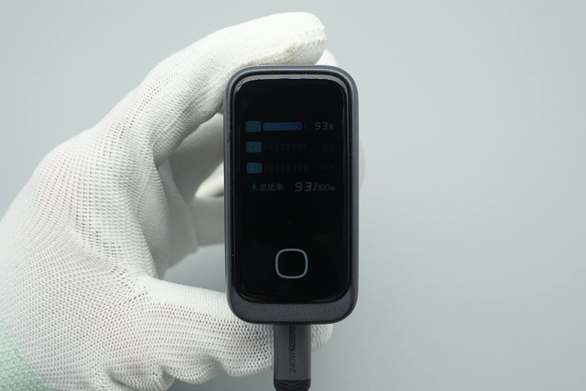
It can also display the output power of each port.
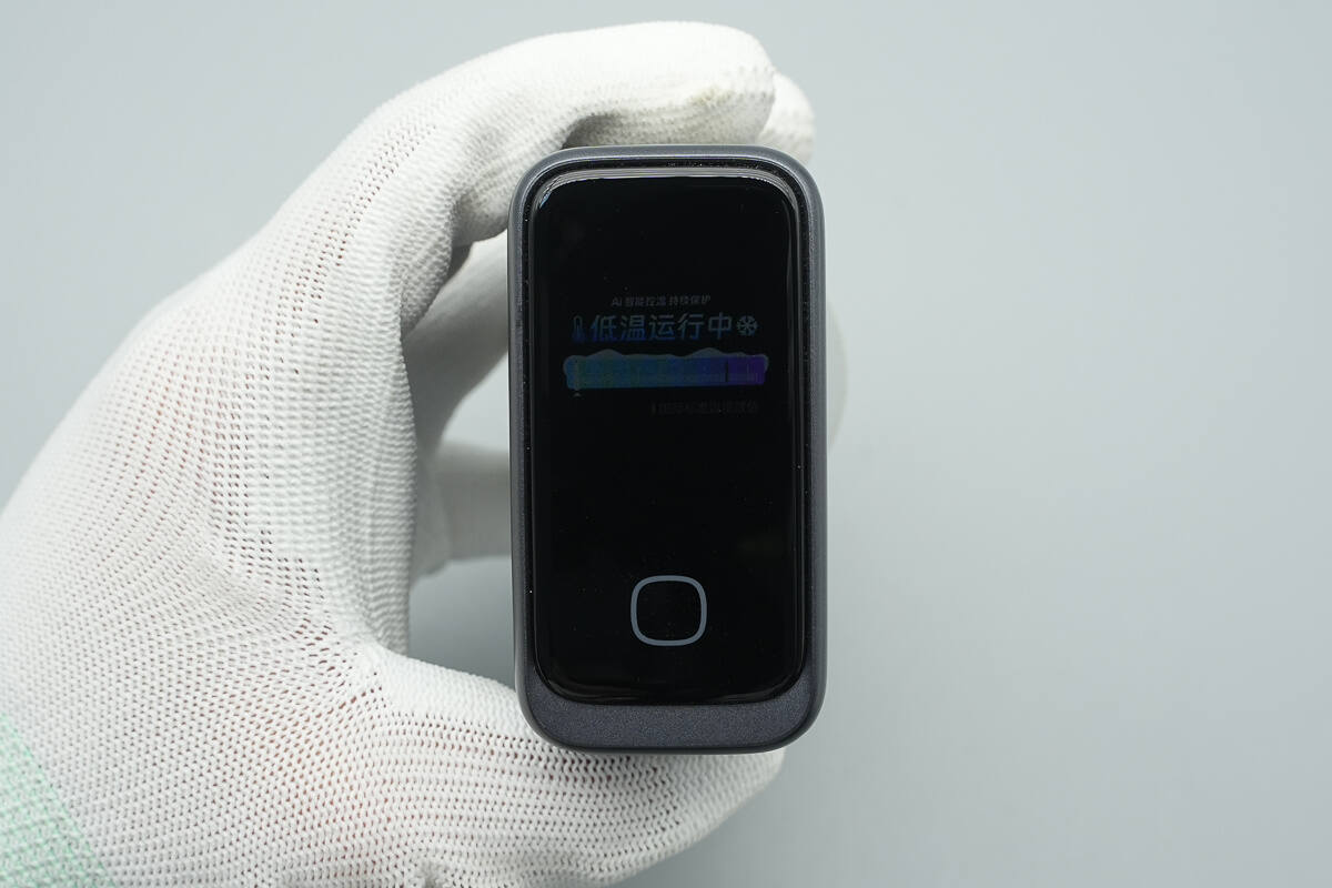
You can check the charging temperature, ensuring safety through visual monitoring.
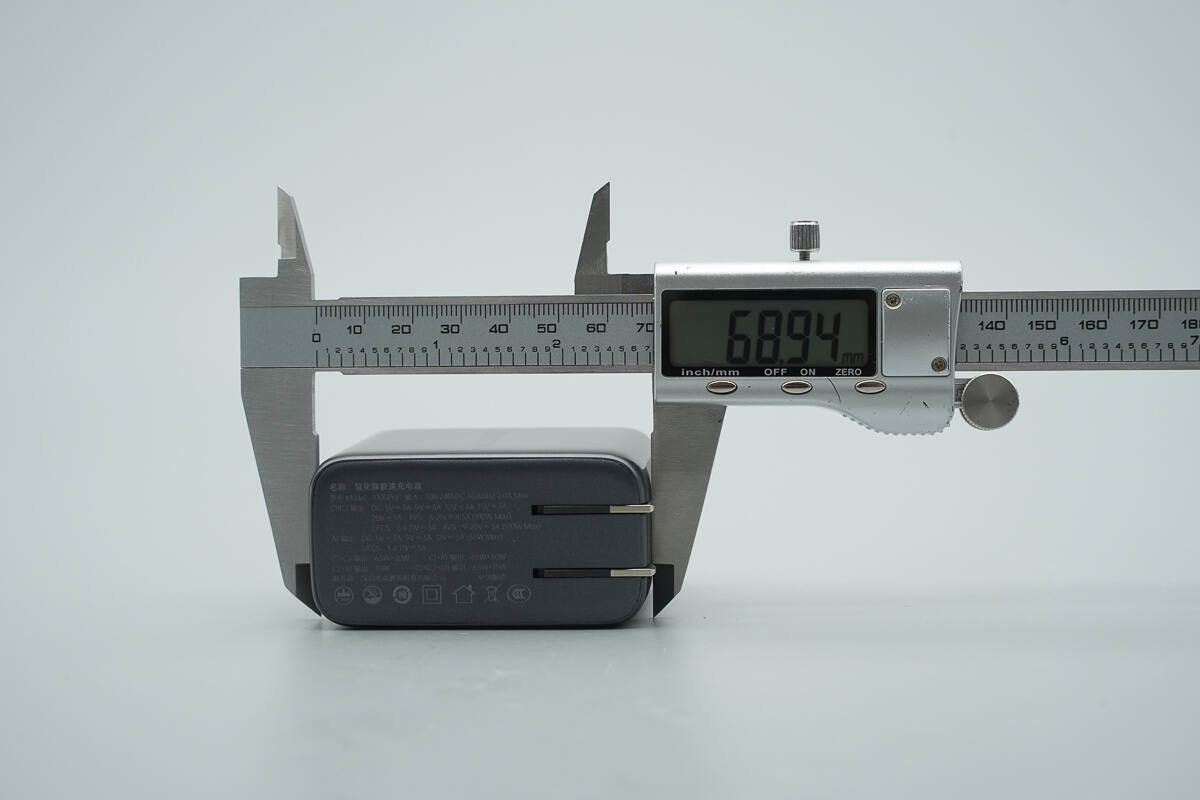
The length of the charger is about 68.94 mm (2.71 inches).
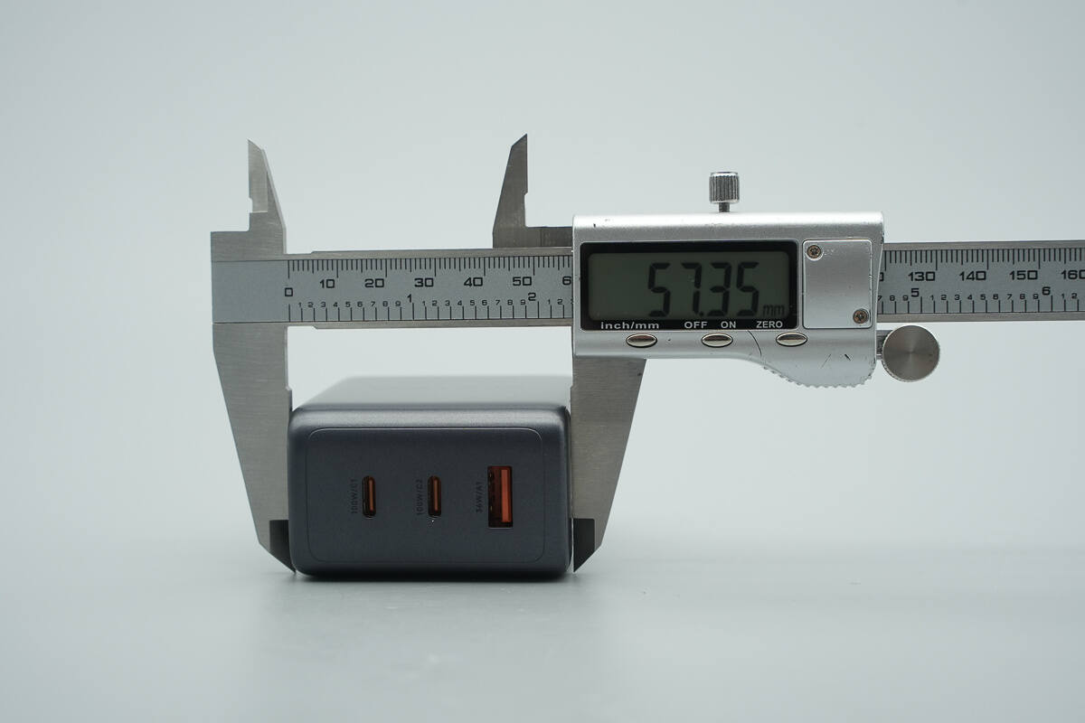
The width is about 57.35 mm (2.26 inches).
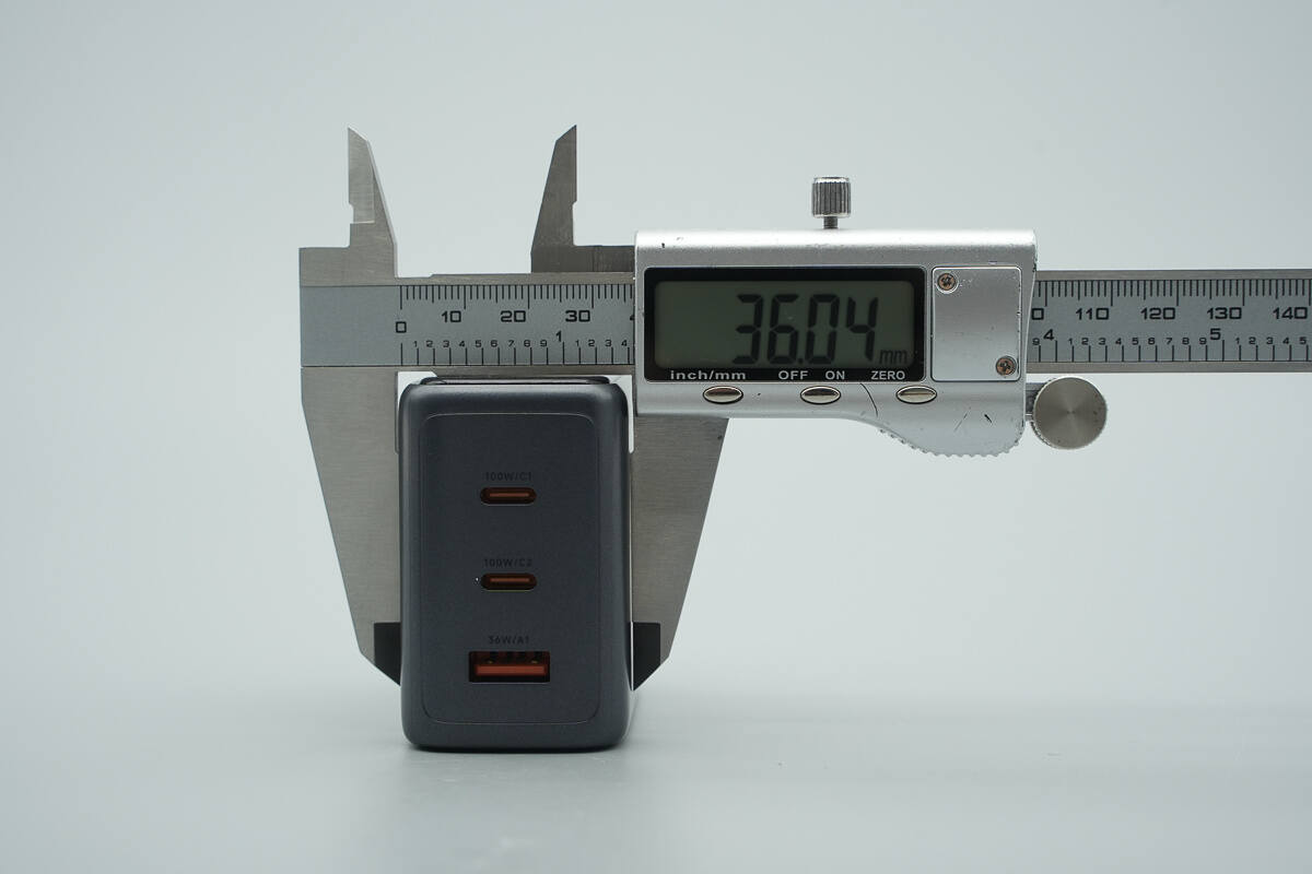
The thickness is about 36.04 mm (1.42 inches).
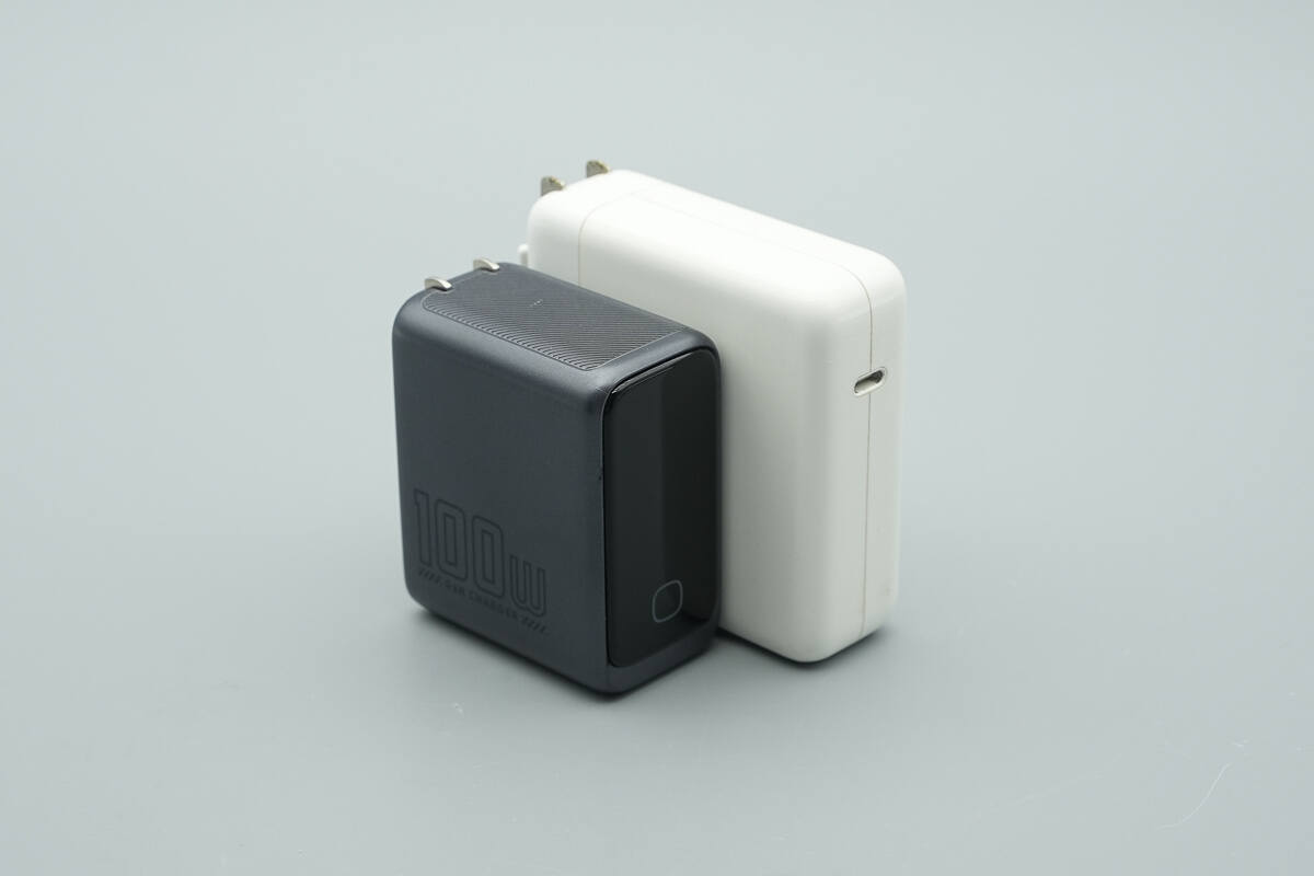
Its size is slightly smaller than that of the Apple 96W charger.
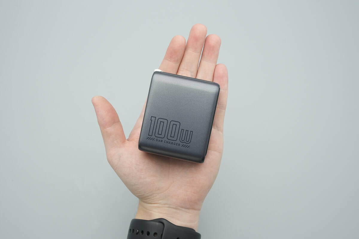
That's how big it is on the hand.

The weight is about 191 g (6.74 oz).
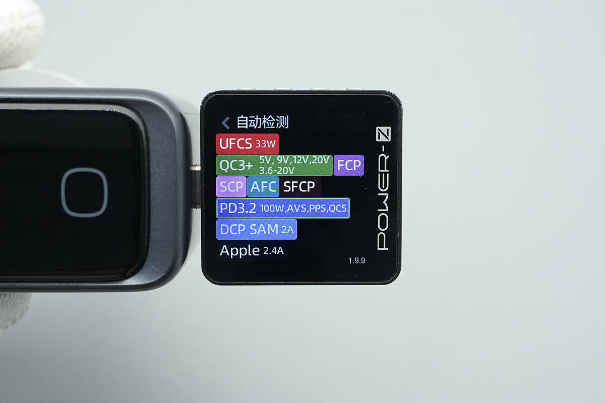
ChargerLAB POWER-Z KM003C shows that the USB-C1 port supports UFCS, QC3+/5, FCP, SCP, AFC, SFCP, PD3.2, PPS, DCP, SAM 2A, and Apple 2.4A charging protocols.
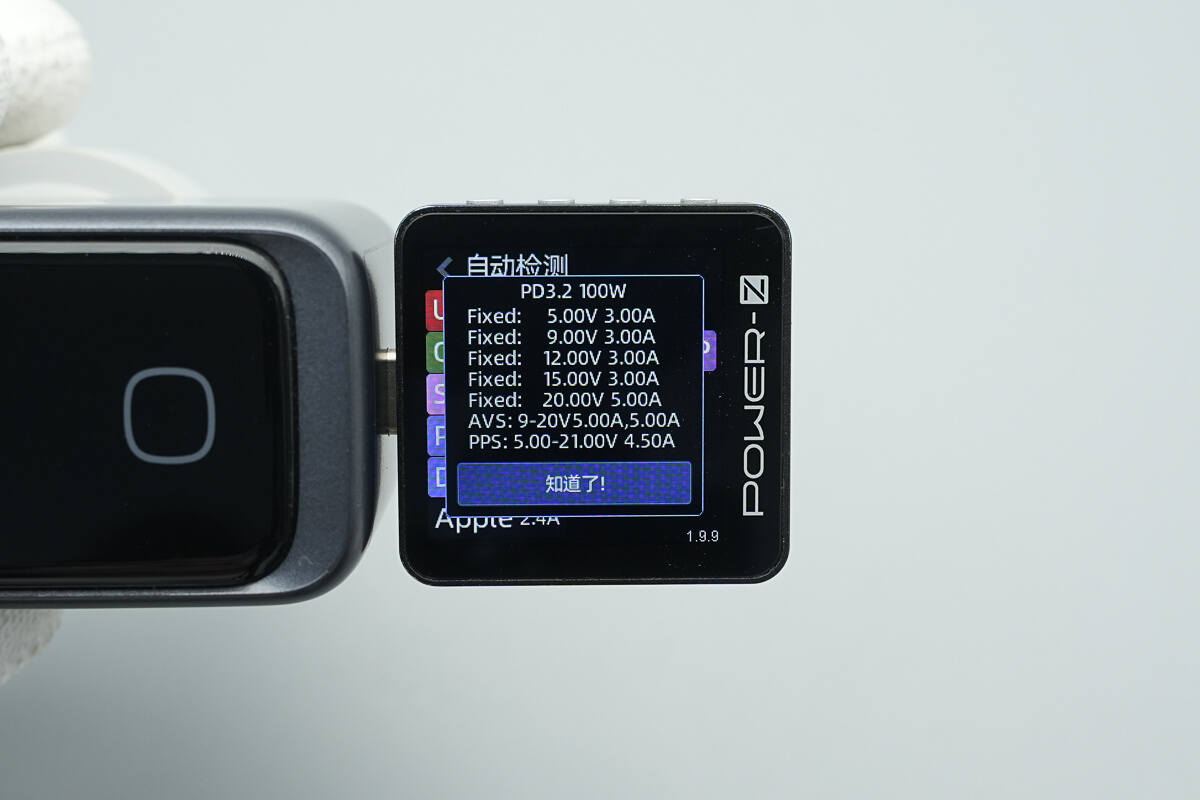
It features five fixed PDOs of 5V3A, 9V3A, 12V3A, 15V3A, and 20V5A, along with a 5-21V4.5A PPS voltage range and a 9-20V5A AVS voltage range.
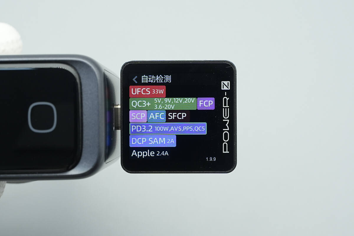
The protocols compatible with the USB-C2 port are the same as those of the USB-C1 port.
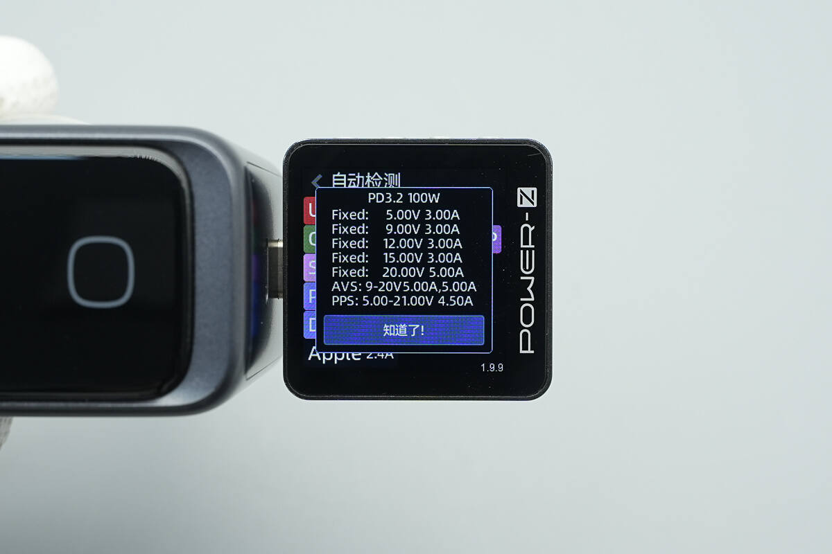
The PDO messages are also the same.
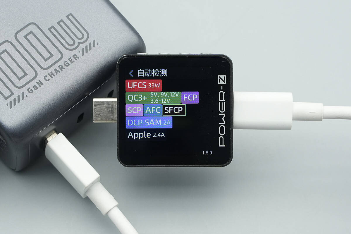
The USB-A supports UFCS, QC3+, FCP, SCP, AFC, SFCP, DCP, SAM 2A, and Apple 2.4A charging protocols.
Teardown
Next, let's take it apart to see its internal components and structure.
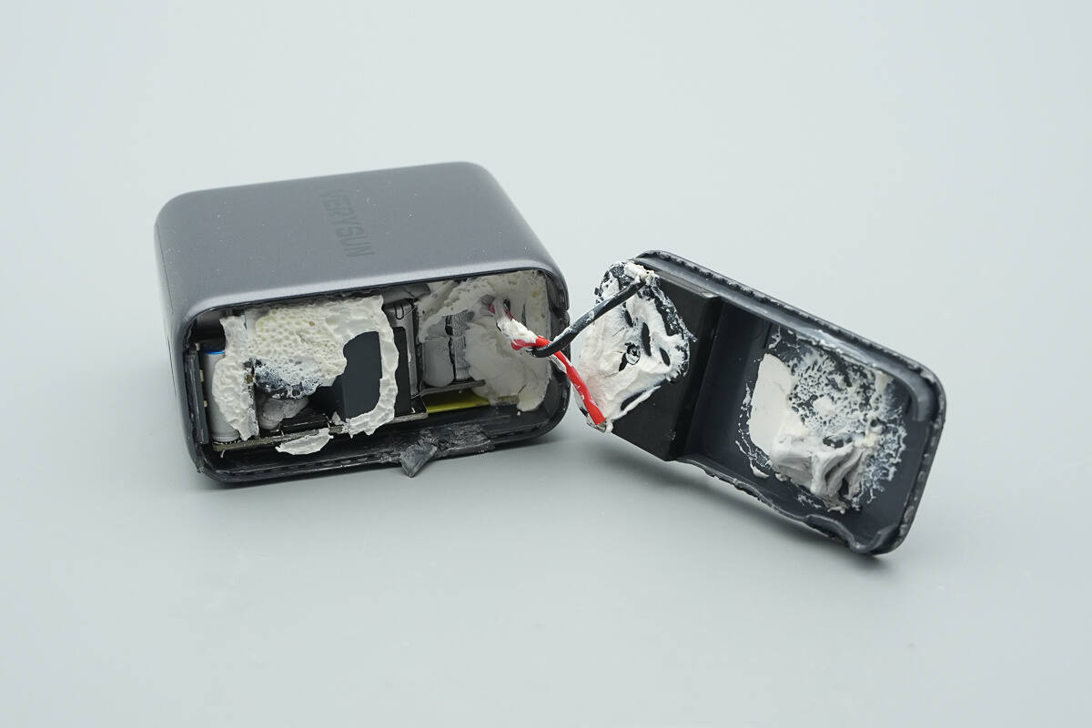
Disassemble the input end shell, with the plug fixed using a plastic plate and screws, and connect it to the PCBA module through wires.
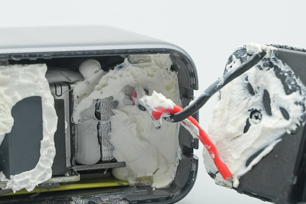
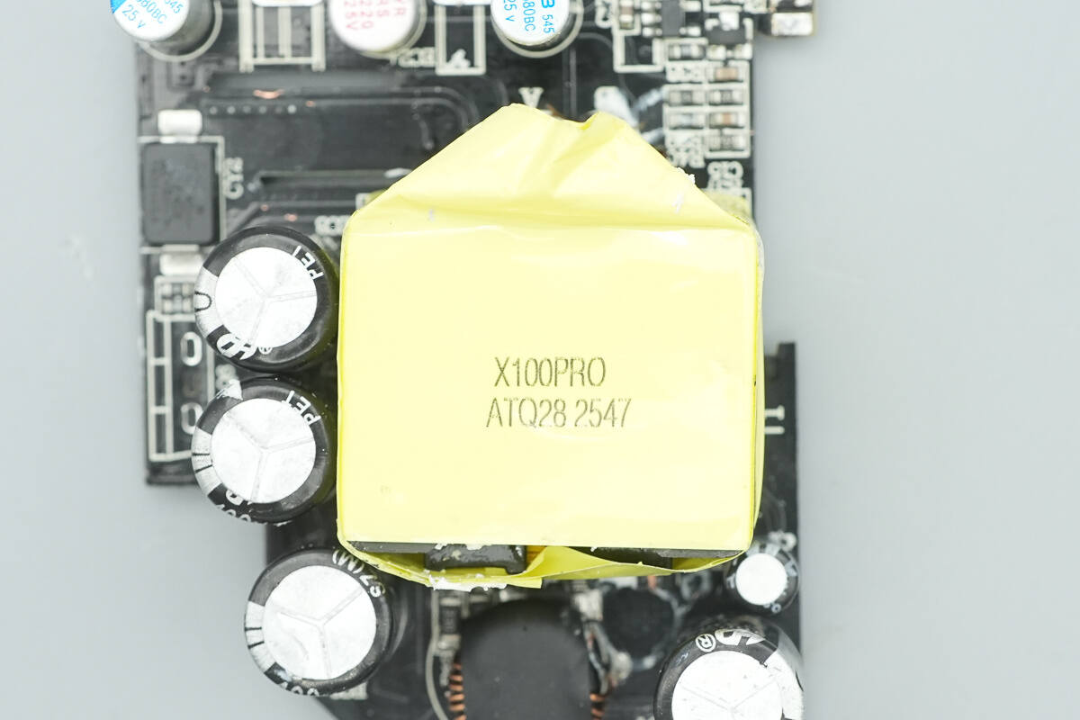
White adhesive is used to fill the gap between the shell and the module for reinforcement.
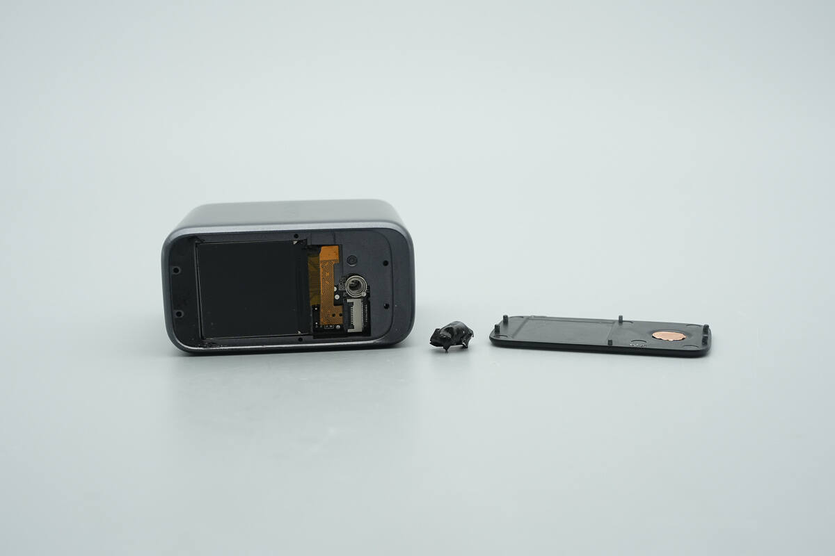
The top cover is removed, and the cover is secured with double-sided adhesive tape.
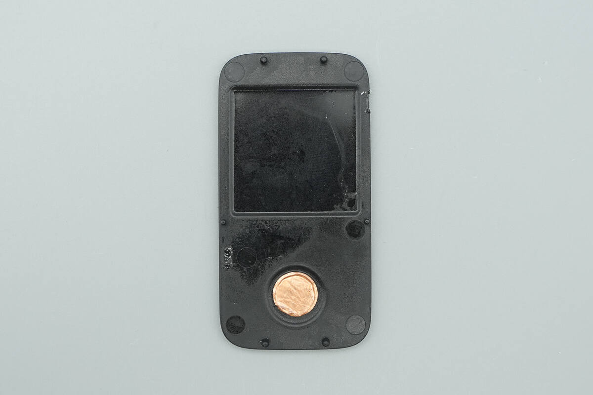
The cover has a screen window, and copper foil is applied to the area corresponding to the touch control button.
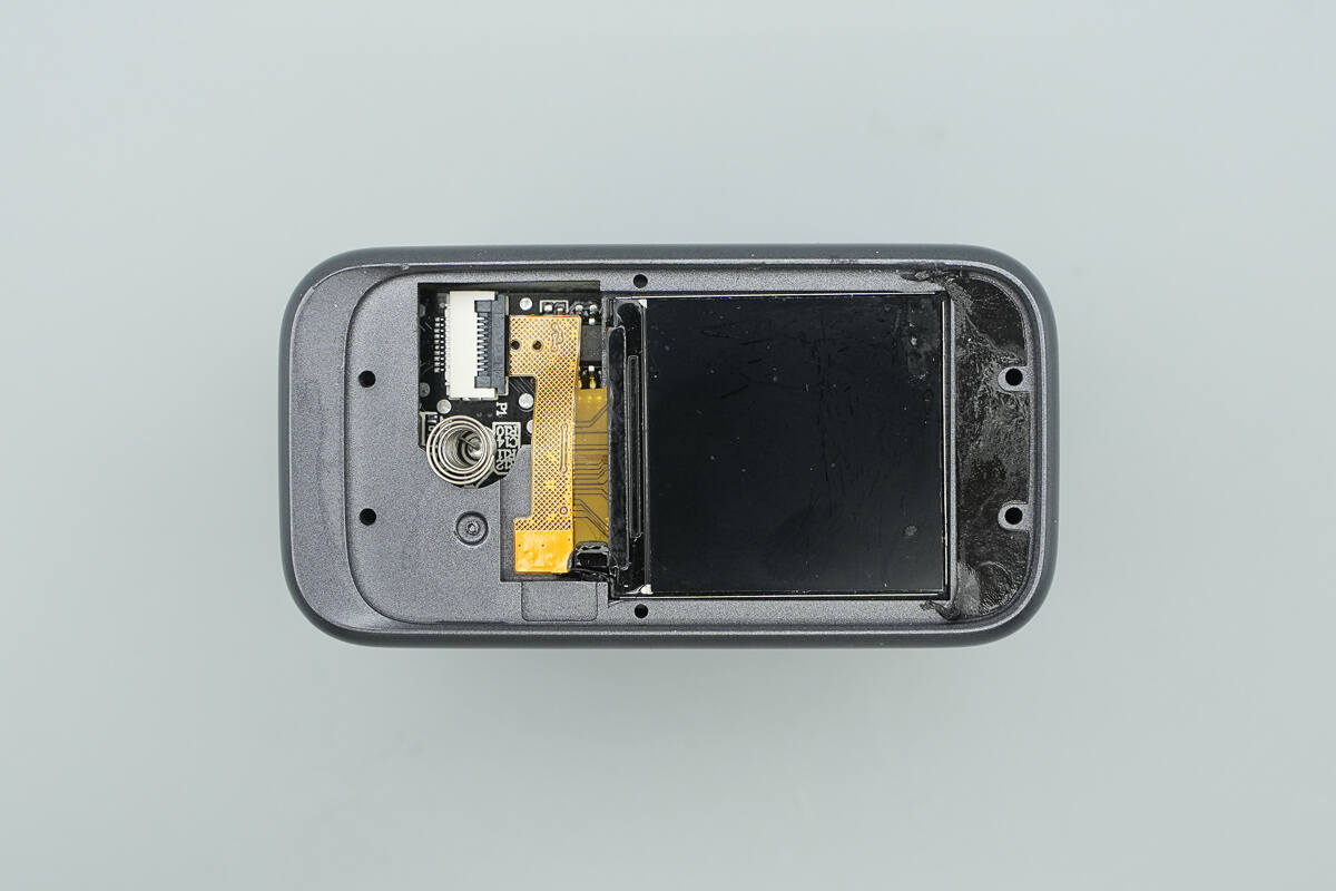
The screen is placed in a recessed slot and connected to the PCBA module via a ribbon cable.

Remove the PCBA module.
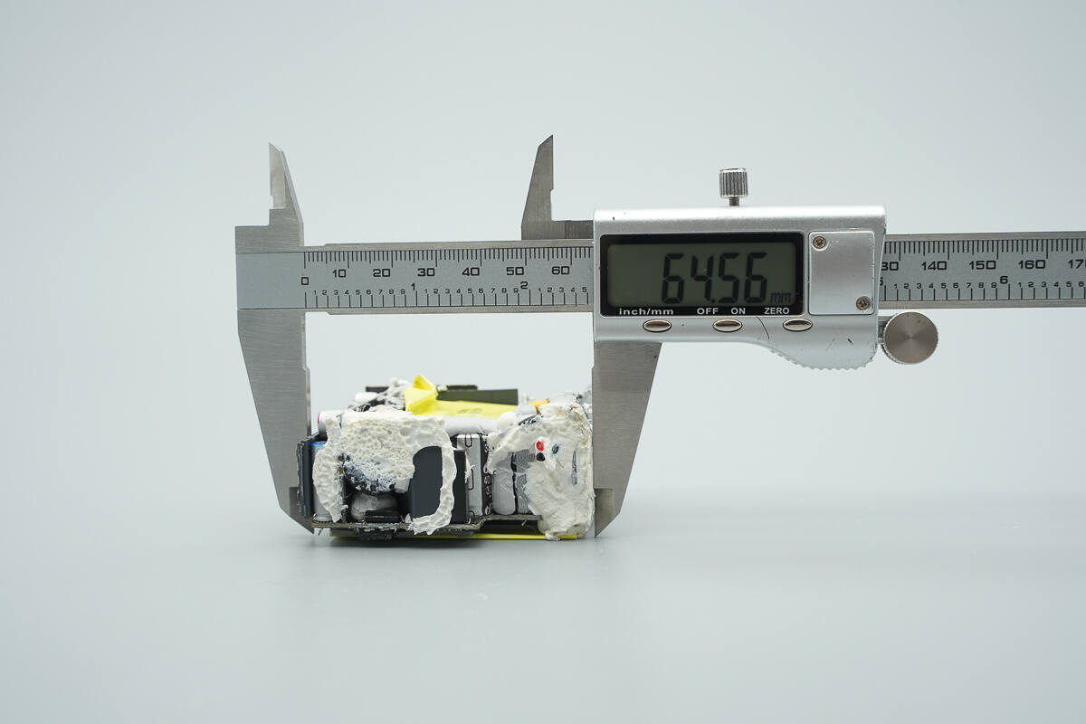
The length of the PCBA module is about 64.56 mm (2.54 inches).
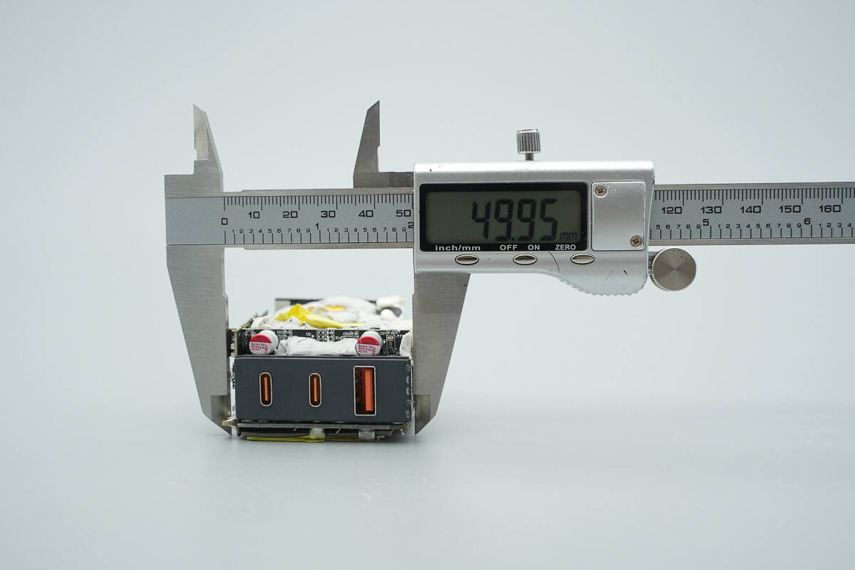
The width is about 49.95 mm (1.97 inches).
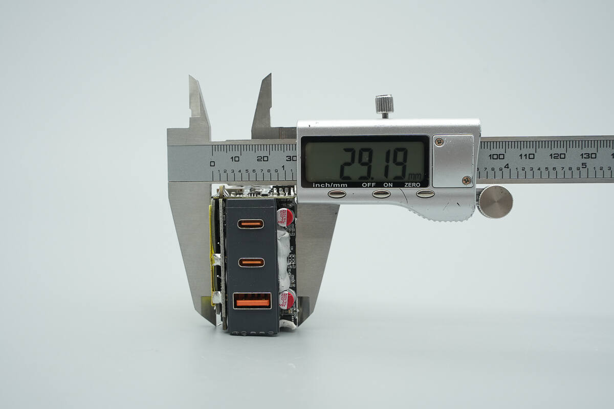
The thickness is about 29.19 mm (1.15 inches).

Thermal adhesive is applied between the components on the front of the module, and Mylar sheets are used around the transformer for insulation.

The bottom of the module is covered with a thermal pad and a heatsink, with the heatsink wrapped in insulating tape.
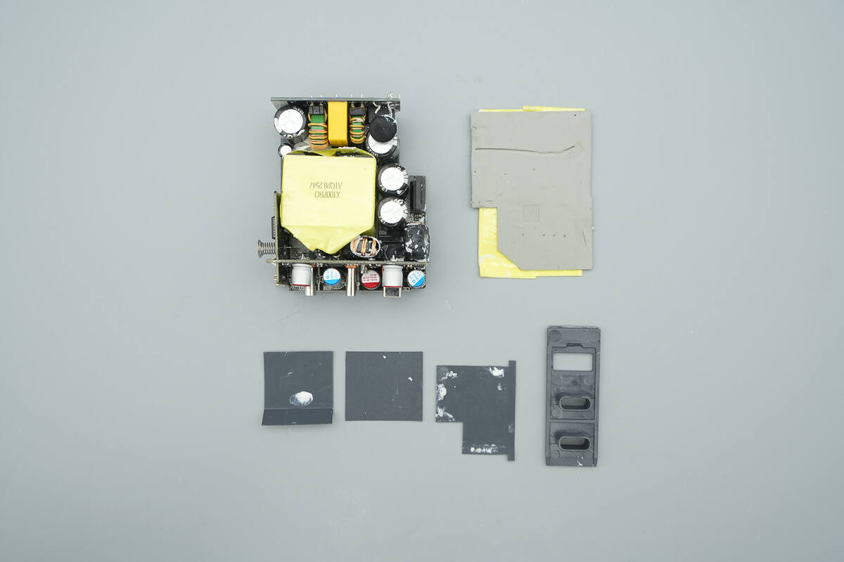
Remove the heatsink, Mylar sheets, and other components, and clean off the thermal adhesive.

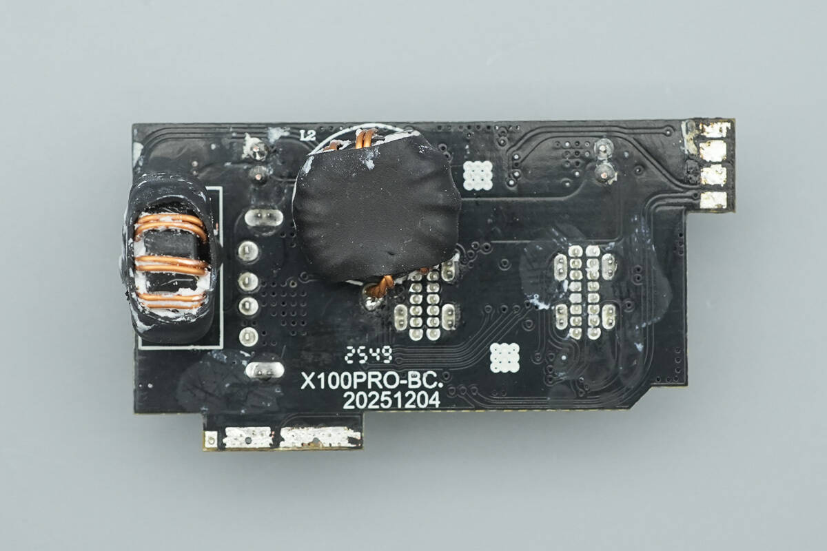
The PCBA module has three small PCBs, and the overall layout is compact.
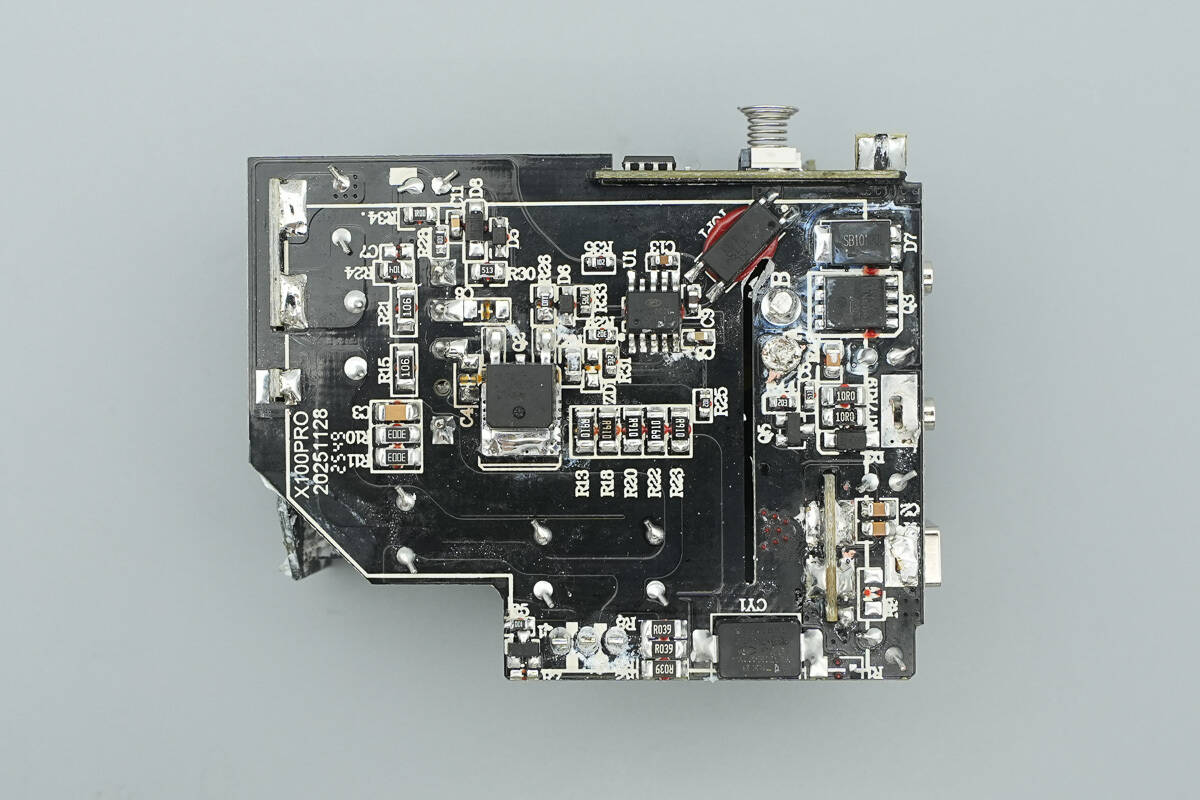
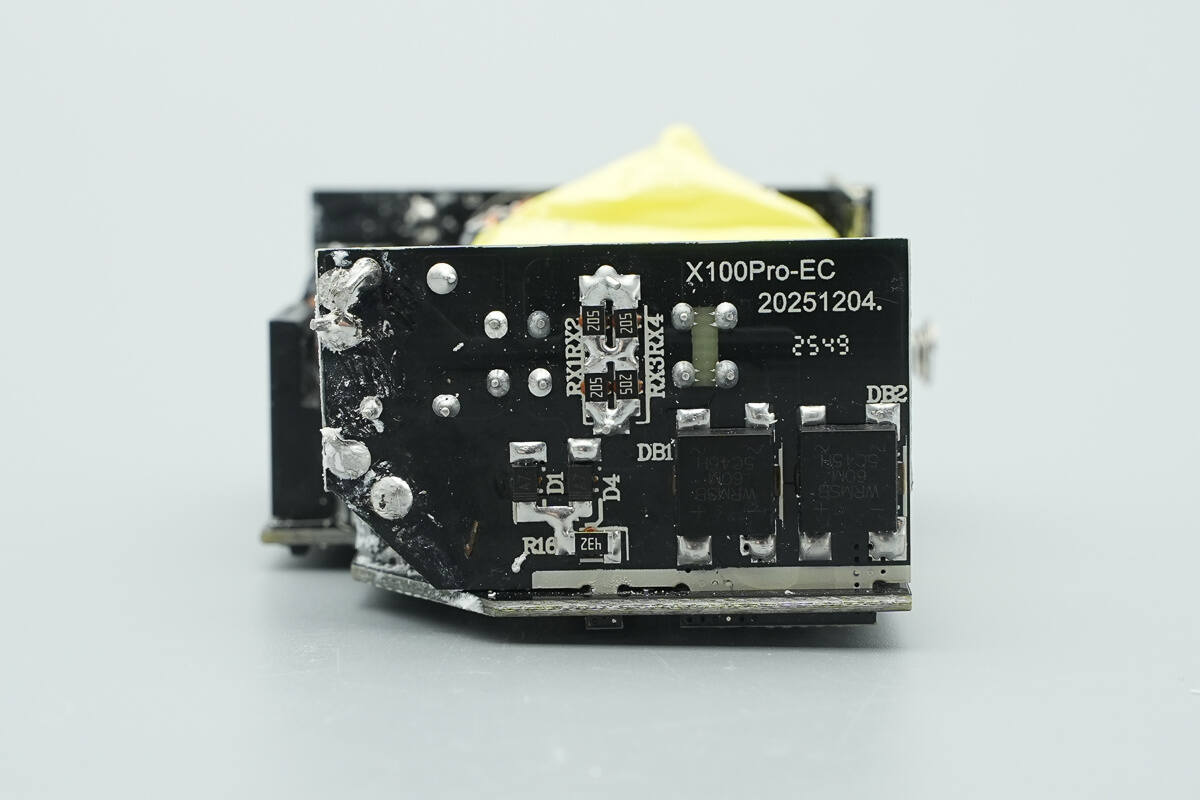
On the back, there are components including the master control chip, primary MOSFET, optocoupler, SMD Y capacitor, and synchronous rectifier.
On the back of the small PCB at the front of the module, there are two bridge rectifiers.
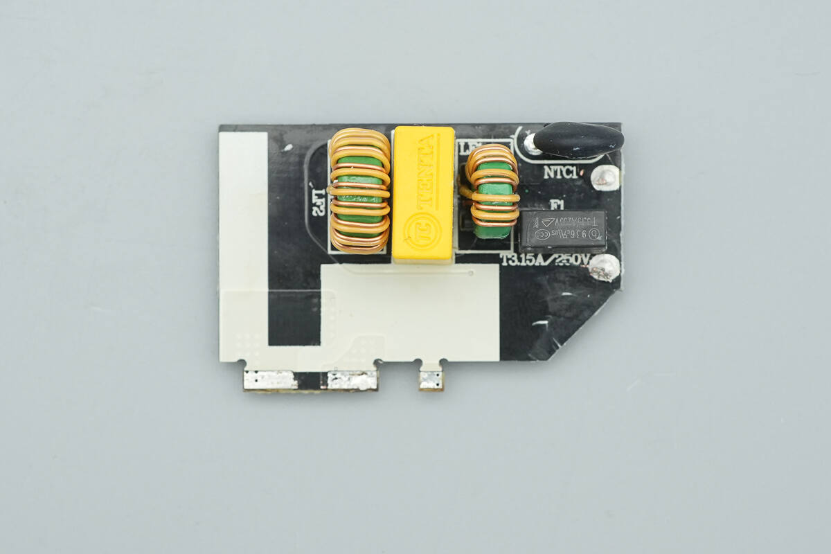
Remove the small PCB, and on the front, there is a time-delay fuse, an NTC thermistor, common mode chokes, and a safety X2 capacitor.

The time-delay fuse is from Betterfuse, with part number 936, and has a specification of 3.15A 250V.
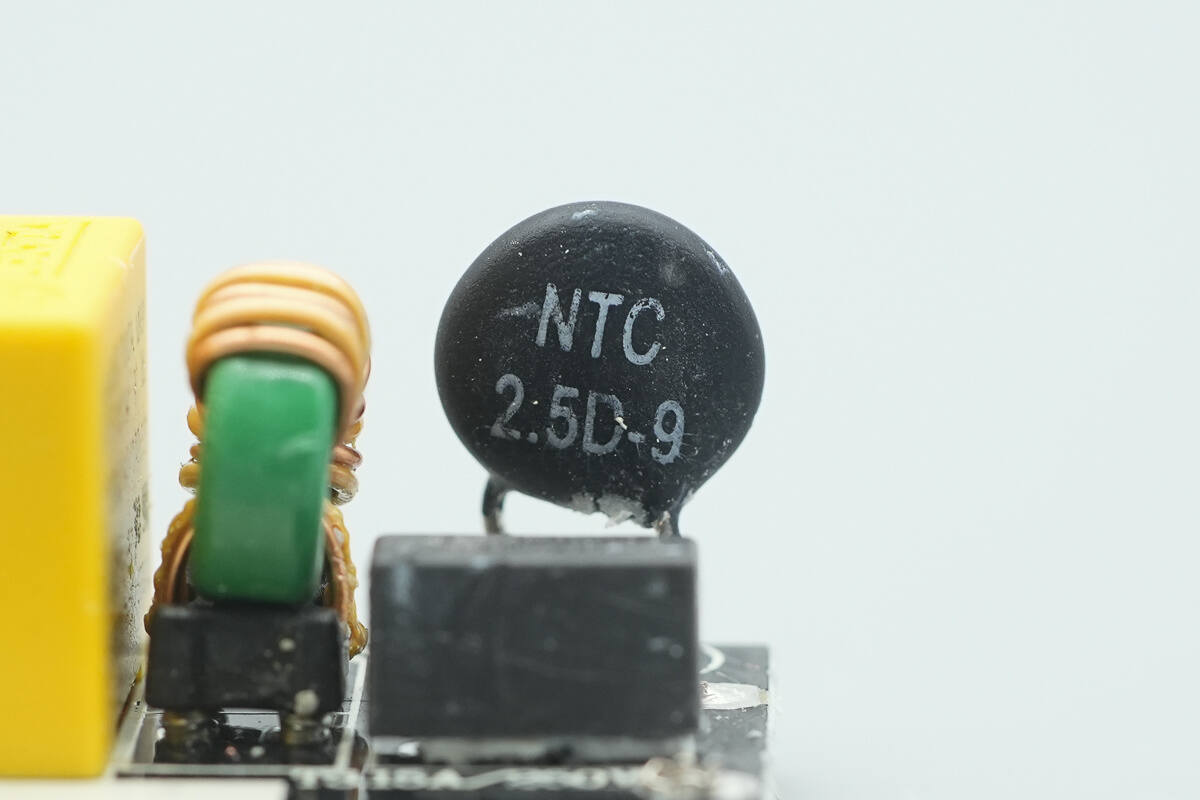
The NTC thermistor is used to suppress inrush current during power-up.

The common mode choke is used to filter out EMI noise.
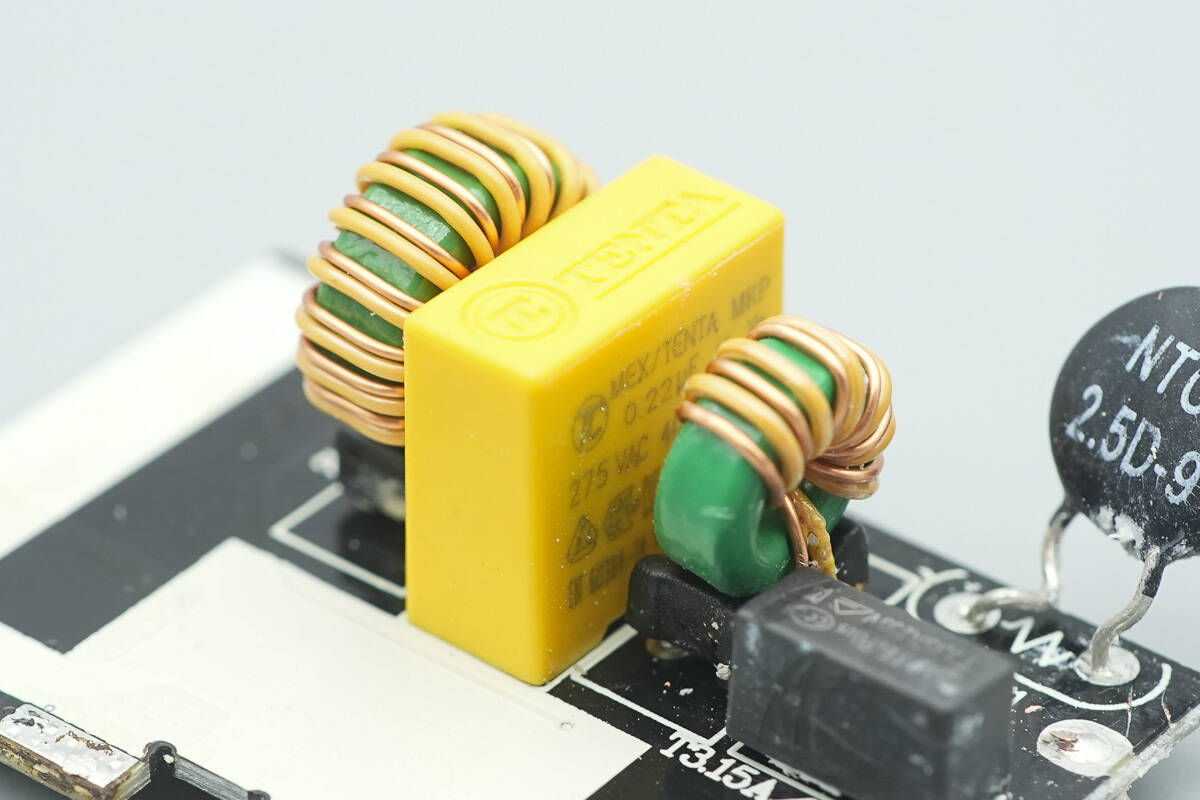
The safety X2 capacitor has a capacitance of 0.22μF.
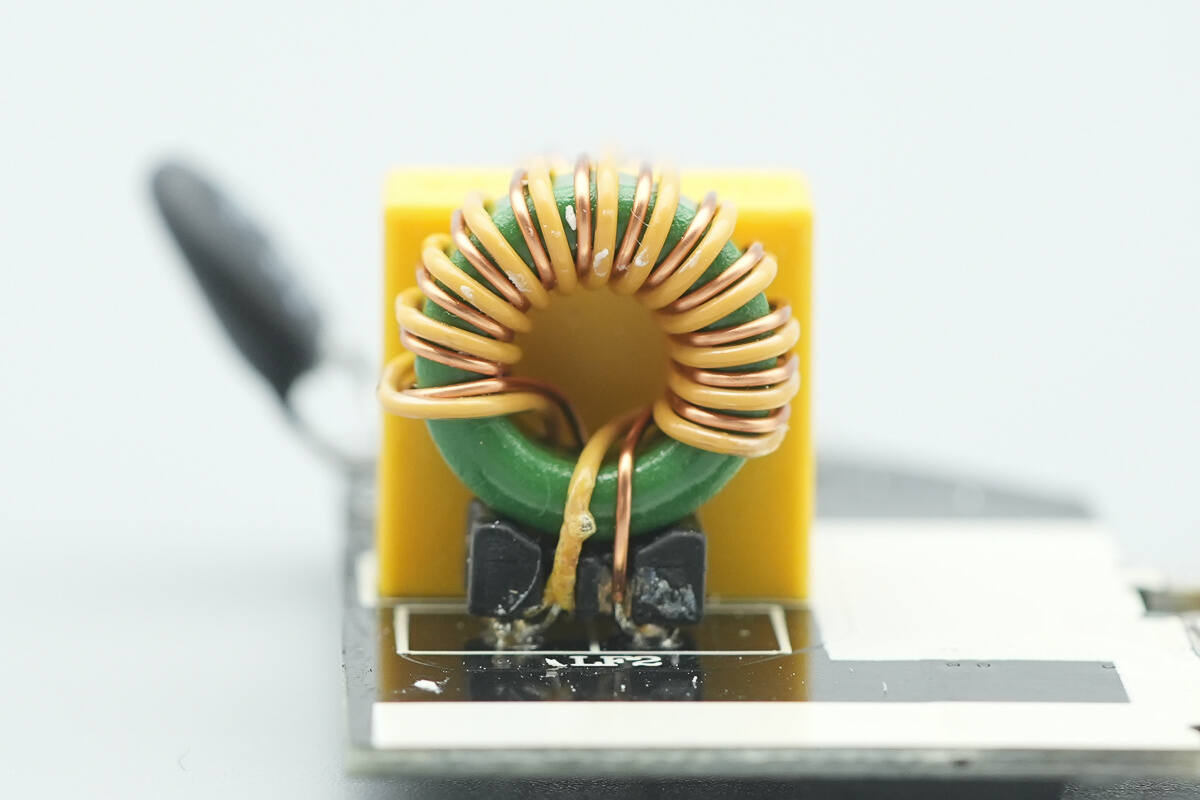
A close-up of the other common mode choke.

The bridge rectifiers are from World Industrial, model WRMSB60M. They are ultra-fast recovery bridge rectifiers with a specification of 6A 1000V, and they use an MSB package.
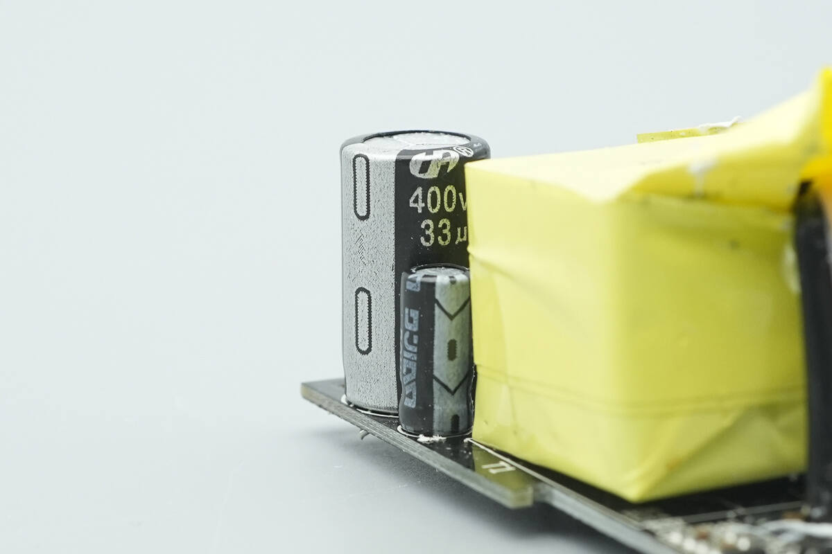
The high-voltage filtering electrolytic capacitor has a specification of 400V 33μF.

The filtering inductor is insulated with a heat-shrink tube.
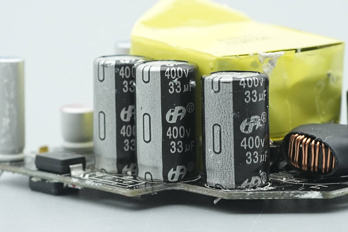
The other three high-voltage filtering electrolytic capacitors all have a specification of 400V 33μF.
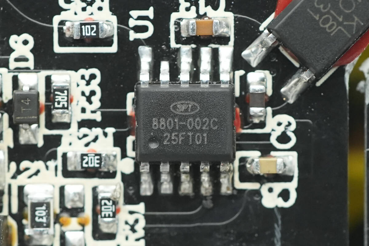
The master control chip is from Si-Power, model SP8801. This is a high-performance mixed-signal control chip suitable for AC/DC flyback topologies. By digitizing key analog signals and performing comprehensive logic processing, it adapts to a wide range of operating conditions and enables more complex functionalities. It is ideal for high-power-density and multi-voltage/current flyback power supply applications.
The chip consists of a state machine-based digital core and analog peripherals, integrating output current calculation and an innovative valley-lock control strategy to ensure efficiency and ripple under different conditions, as well as constant or constant power output current limiting. This meets the safety requirements of LPS (Limited Power Source) or multi-port charging.
The chip supports active CCM/QR/DCM multi-mode switching and optionally features PFC-less switching capacitor functionality, which is helpful for chargers and adapter products with input power >75W, meeting CLASS A harmonic requirements. It also integrates a high-voltage startup module, with standby power consumption complying with Level 6 energy efficiency standards.

The SP8801 integrates comprehensive protection features, including primary current limit protection, overload protection, internal over-temperature protection, sampling resistor short-circuit protection, output rectifier short-circuit protection, input overvoltage and undervoltage protection, output overvoltage and undervoltage protection, VDD overvoltage protection, and ZCD open-circuit and short-circuit protection. The chip is packaged in an SSOP10 form factor.
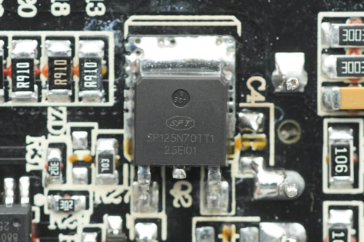
The primary MOSFET is also from Si-Power, model SP125N70TT1. This is an advanced GaN FET with a working voltage of 700V and a normally closed characteristic. This device enables higher power density and is suitable for high-frequency DC-DC converters and fast-charging applications.
The SP125N70TT1 complies with the EU RoHS environmental standards and has passed 100% high-temperature reverse-bias and high-temperature gate-bias reliability testing. It also holds a complete functional reliability certification.
Here is the information about Si-power SP125N70TT1.
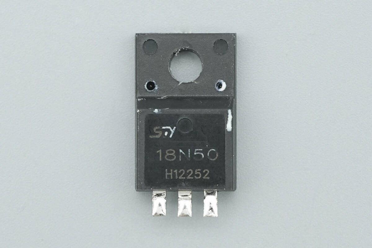
The MOSFET marked with 18N50 is packaged in a TO220F form factor.
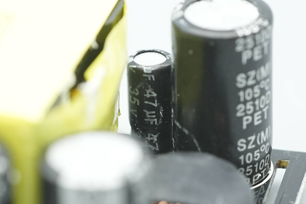
The capacitor that powers the master control chip has a specification of 35V 47μF.
Close-up of the transformer.
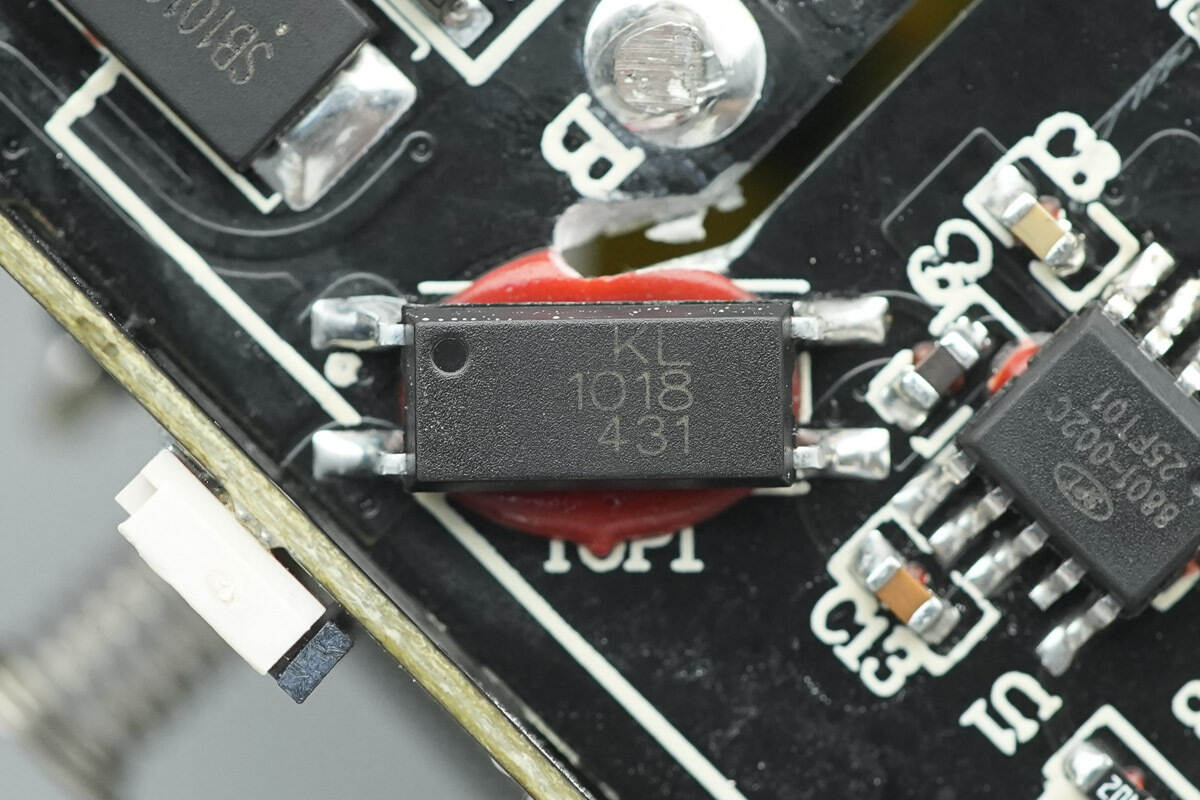
The KL1018 optocoupler is used for output voltage feedback.

The SMD Y capacitor is from TRX. Its compact size and light weight make it well-suited for high-density power products such as GaN fast chargers. The part number is TMY1471K.
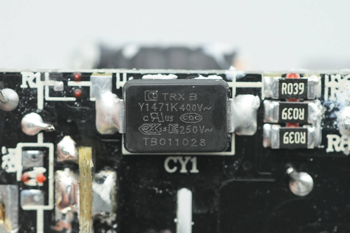
Another TRX SMD Y capacitor has the same part number, TMY1471K.
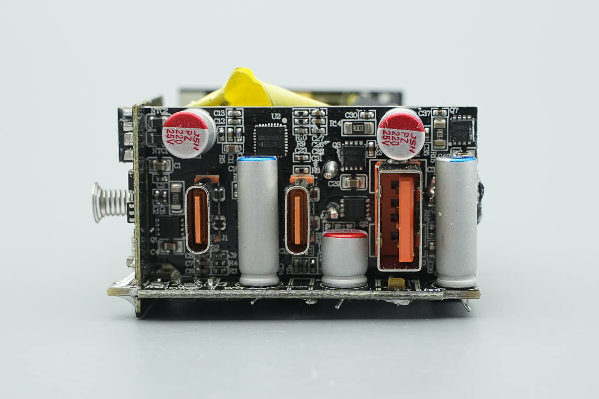
The three USB sockets are soldered onto a separate small PCB.
Remove the small PCB, and on the back, there are two buck inductors, both insulated with heat shrink tubing.
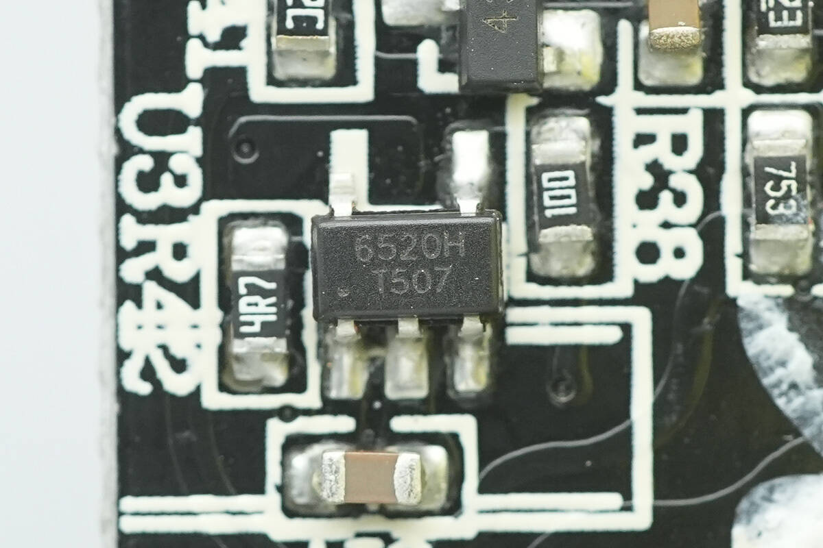
The synchronous rectifier controller is from Si-Power, model SP6520H. In low-voltage, high-current switch-mode power supply applications, it easily meets Level 6 energy efficiency standards, making it an ideal solution for ultra-low on-resistance rectifier devices. The chip supports switching frequencies of up to 500kHz and is compatible with various switch-mode power supply operating modes such as CCM/QR/DCM.
The SP6520H features a self-powered circuit and can be flexibly placed on either the positive or negative side. When placed on the positive side, no additional auxiliary windings are required. The 10ns turn-off delay and up to 4A pull-down current help the system reliably operate in CCM mode. Its unique turn-on and turn-off mechanism maximizes the conduction time of the external MOSFET, resulting in higher conversion efficiency. The chip is packaged in a SOT23-5 form factor.
Here is the information about Si-power SP6520H.
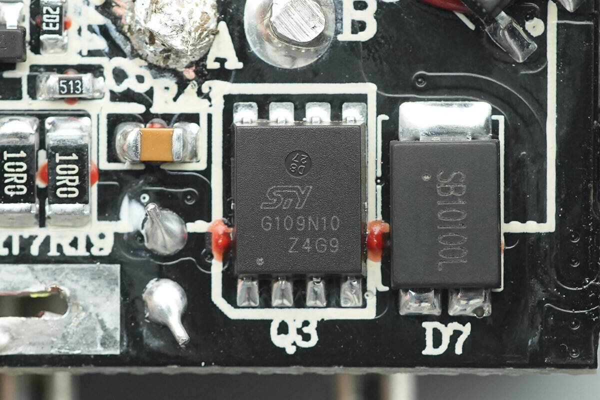
The synchronous rectifier, marked with G109N10, is packaged in a DFN 5x6 form factor.
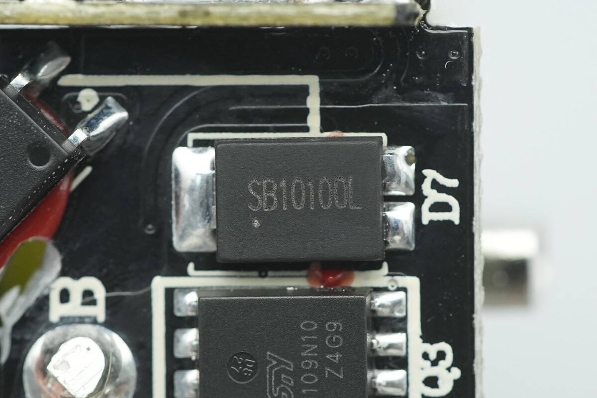
An SB10100L Schottky diode is paralleled next to it to improve light-load efficiency.
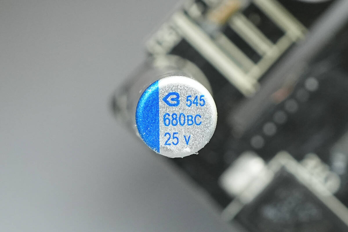
The output filter solid capacitor is from BERYL, with a specification of 25V 680μF.
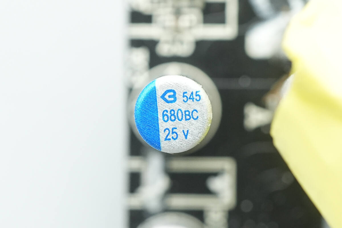
The other one is identical.
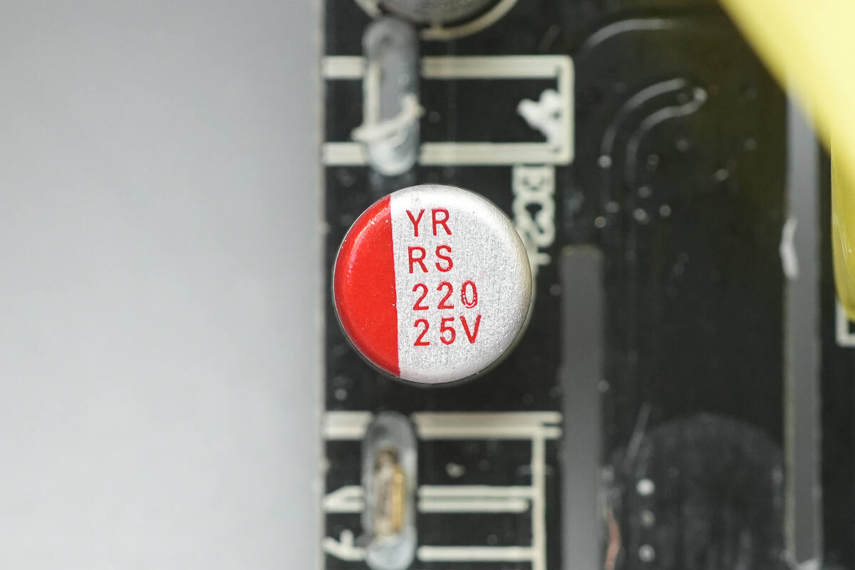
The third solid capacitor has a specification of 25V 220μF.
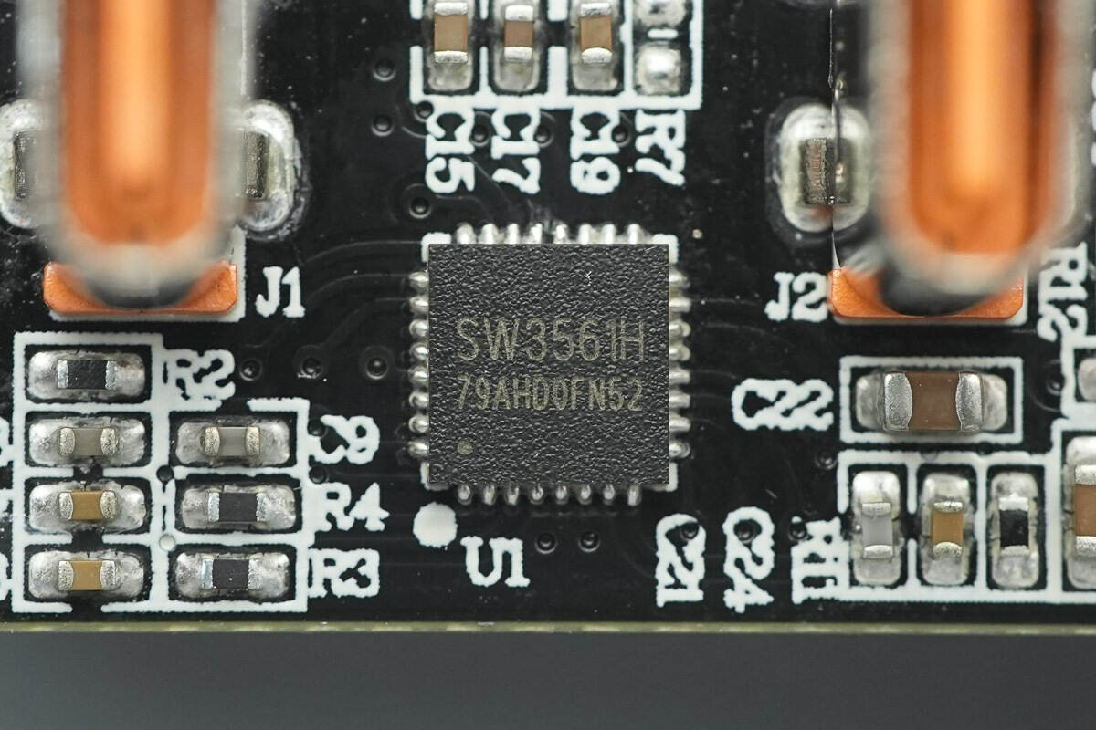
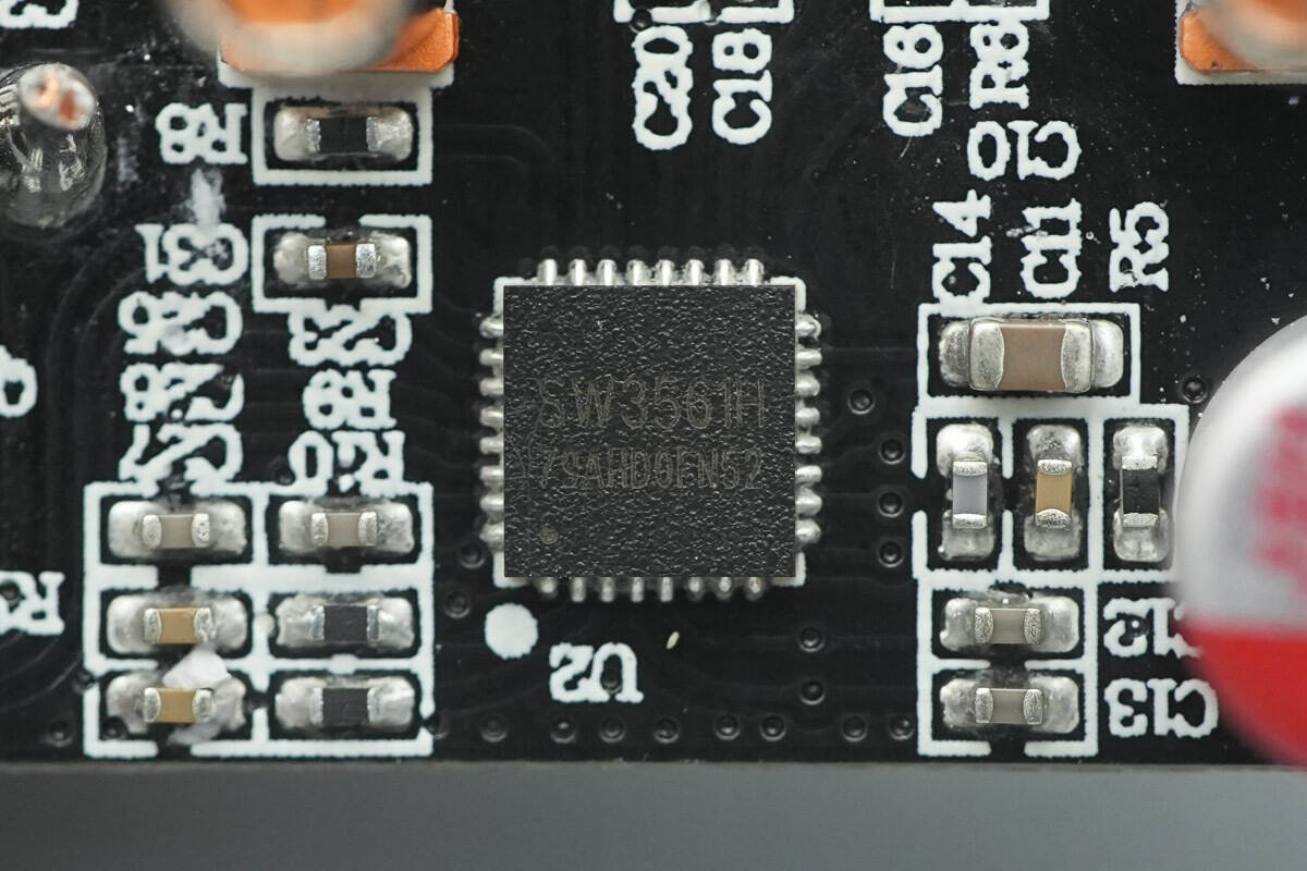
The buck protocol chip for the USB-C1 port is from iSmartWare, model SW3561H. It supports dual USB-C output ports, integrates a high-efficiency synchronous buck converter, supports 20V 5A power output, and is compliant with USBPD 3.1 SPR. The chip integrates an ARM Cortex-M0 core and Type-C logic, supporting PD 3.1, QC, SCP, UFCS, and other fast charging protocols, as well as customizable fast charging protocols.
The SW3561H supports dual USB-C port routing control and line loss compensation. When paired with two synchronous buck MOSFETs and the corresponding VBUS MOSFETs for each port, it enables dual-port buck output. The integrated buck converter operates at a default frequency of 180kHz, but supports customizable frequencies and can deliver up to 100W of power, catering to compact designs. The chip also includes comprehensive protection features, such as overheat protection, input/output overvoltage/undervoltage protection, output overcurrent protection, and data pin overvoltage protection. It comes in a QFN-32 package.
Here is the information about iSmartWare SW3561H.
The buck protocol chip for the USB-C2 and USB-A ports is also the iSmartWare SW3561H.
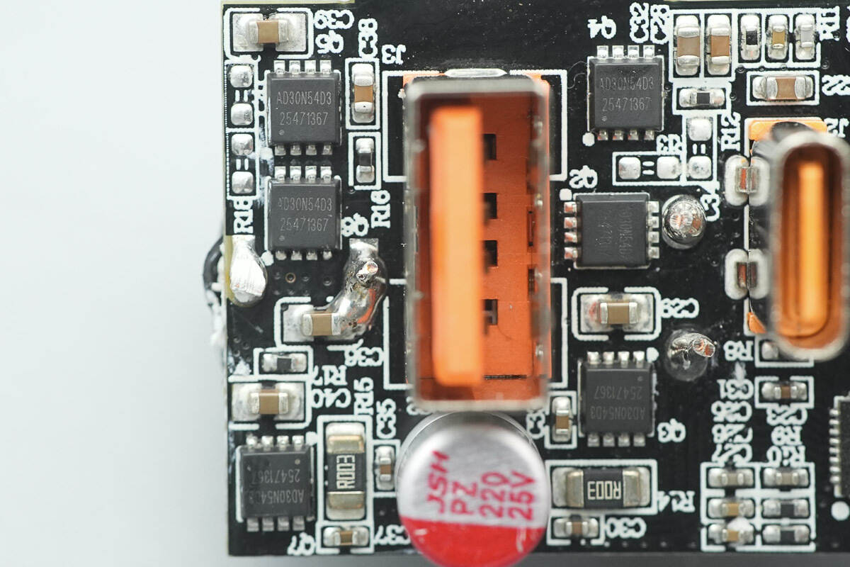
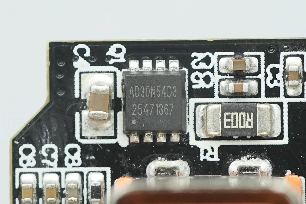
The synchronous buck MOSFETs for the two buck circuits and the output VBUS MOSFETs for the three USB ports all use the ADAMANT AD30N54D3.
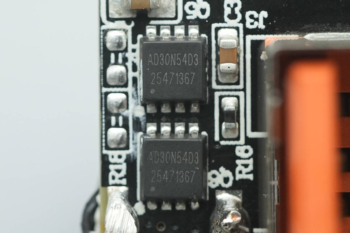
The synchronous buck MOSFETs are from ADAMANT, model AD30N54D3. These are NMOS transistors with a voltage rating of 30V, a Rds(on) of 5.7mΩ, and are packaged in a PPAK 3x3 form factor.
A close-up of the output VBUS MOSFET for the USB-C1 port.
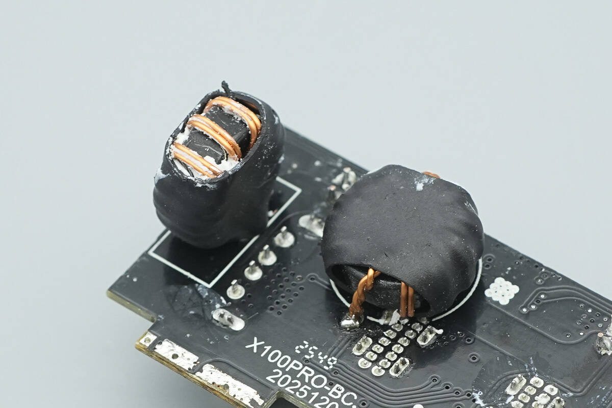
A close-up of the two buck inductors.
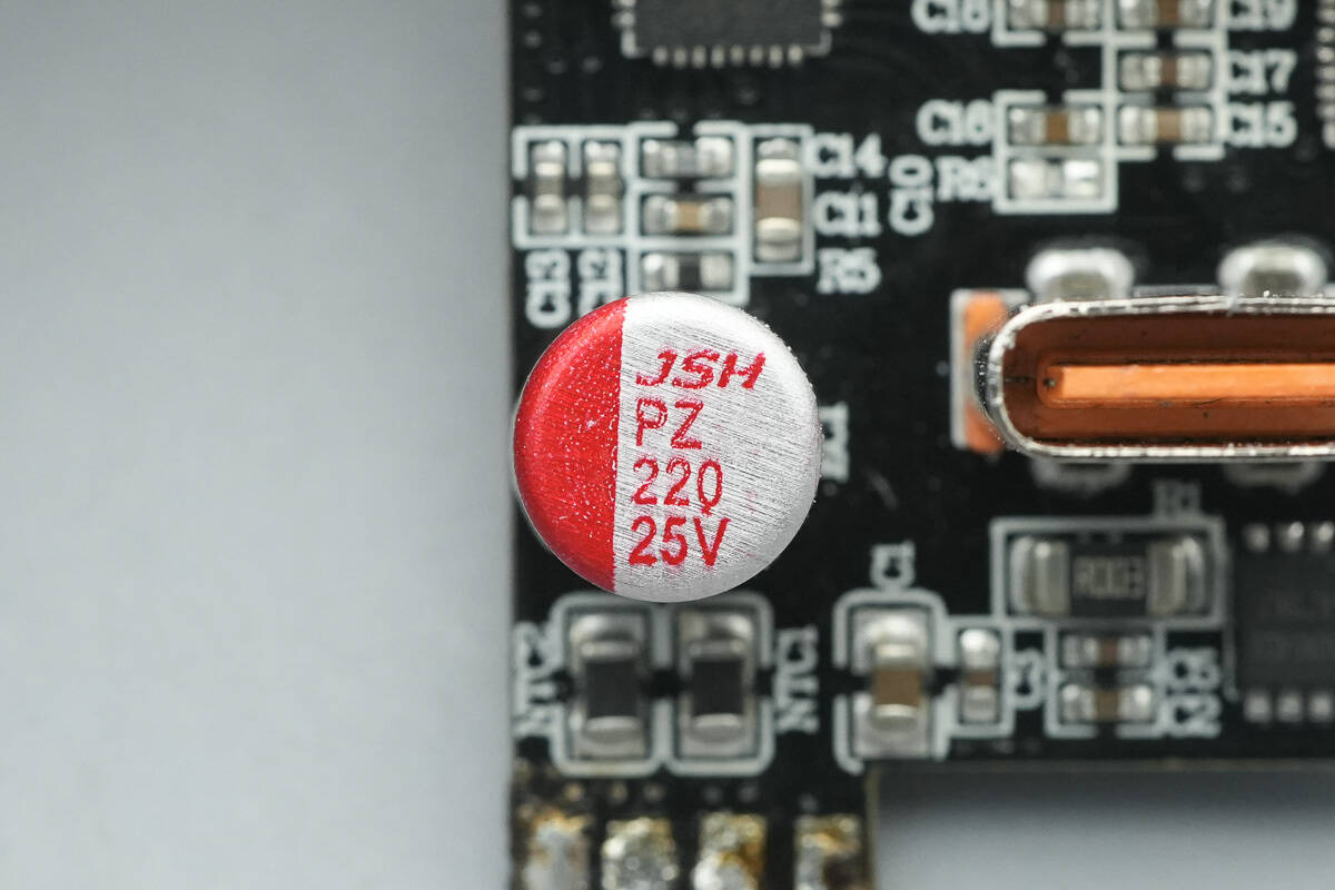
The secondary buck output filter solid capacitor is from JSH, with a specification of 25V 220μF.
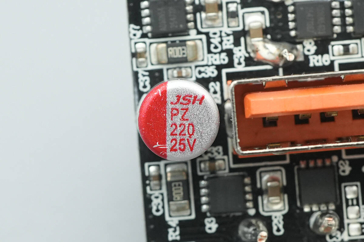
The other solid capacitor has the same part number.
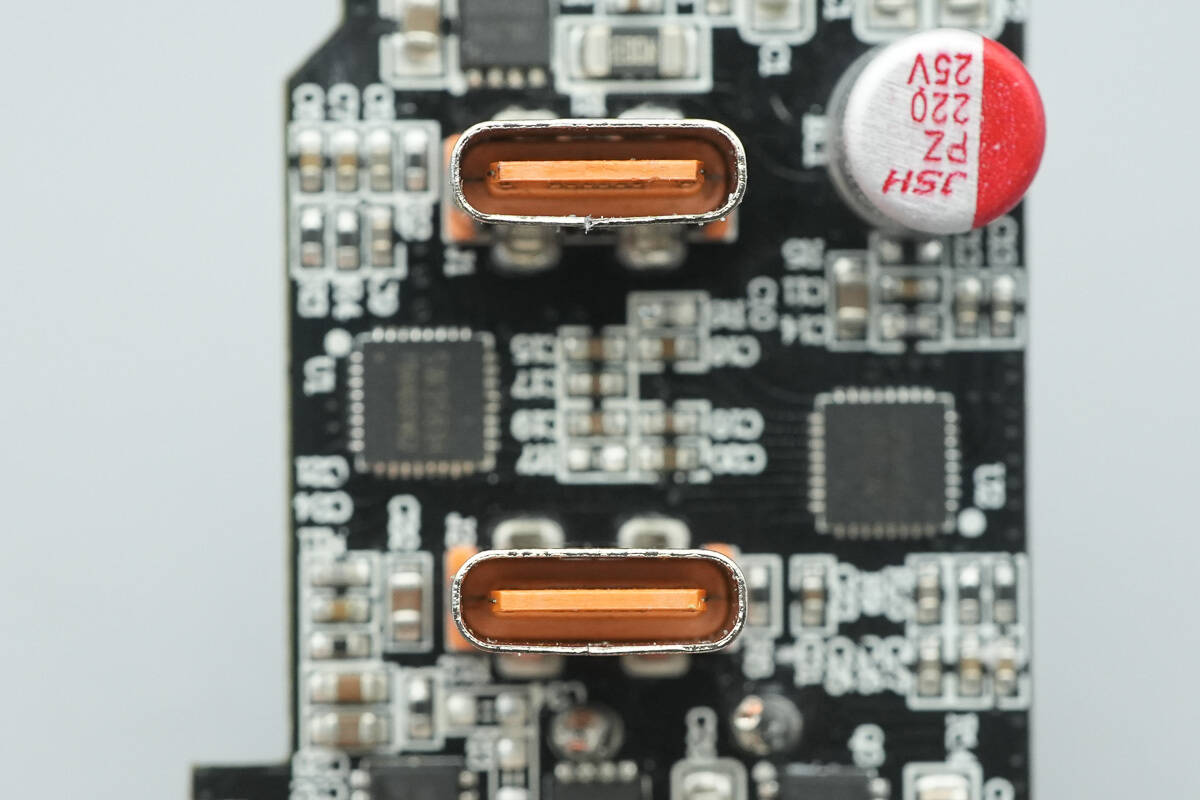
A close-up of the two USB-C sockets.
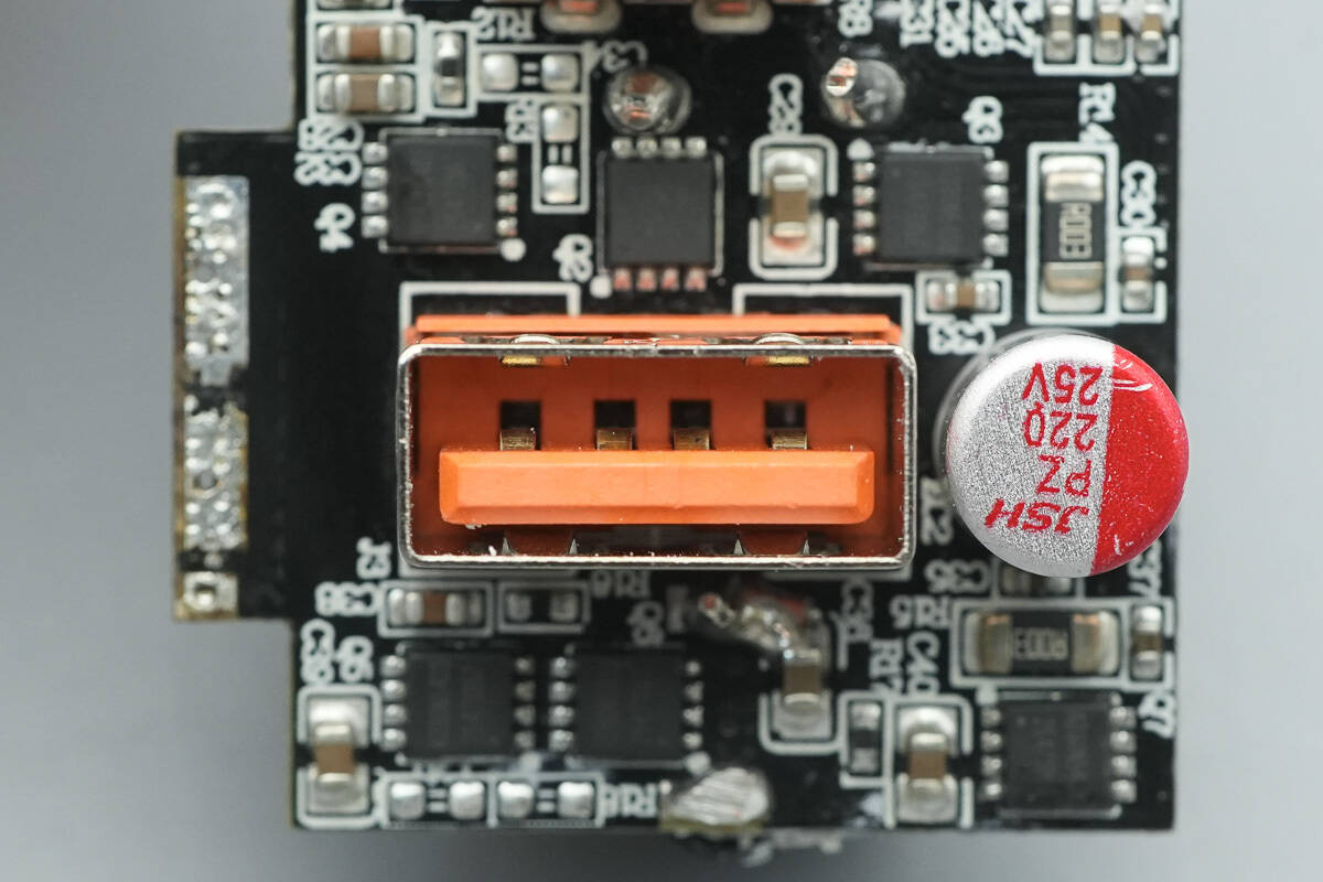
A close-up of the USB-A socket.
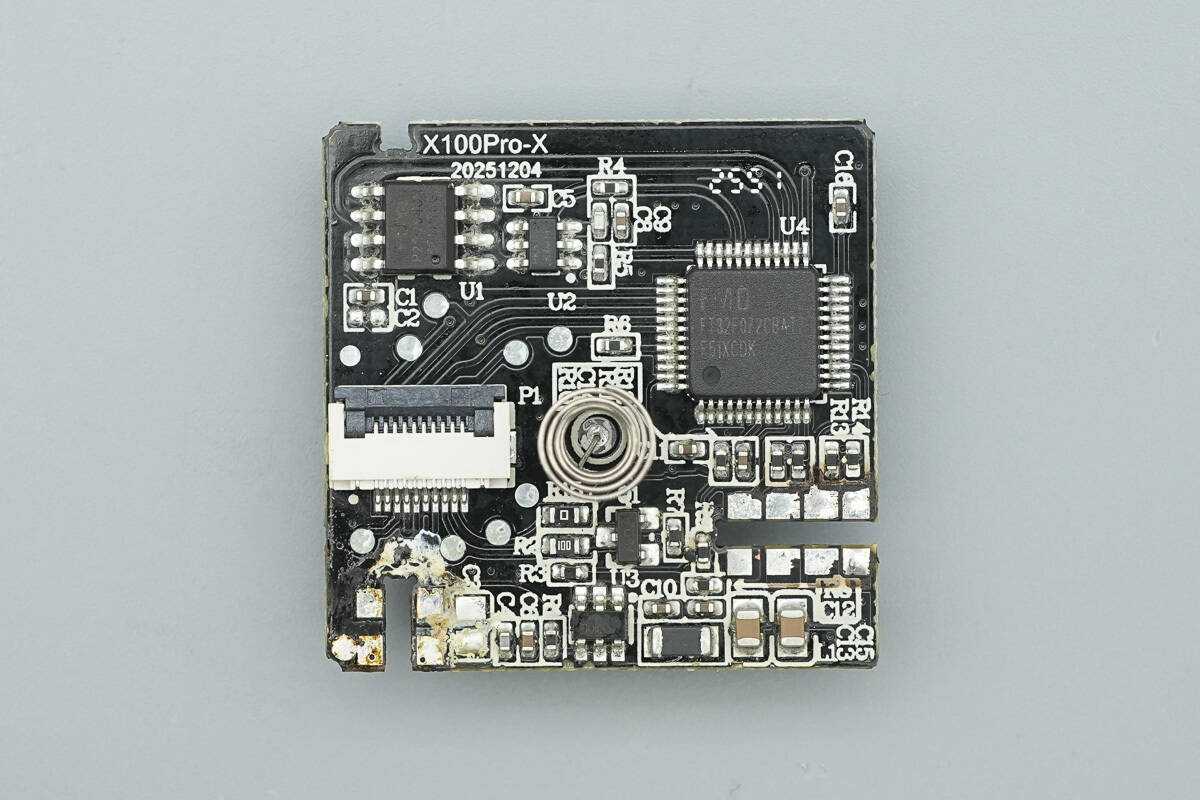
A close-up of the screen control small PCB.
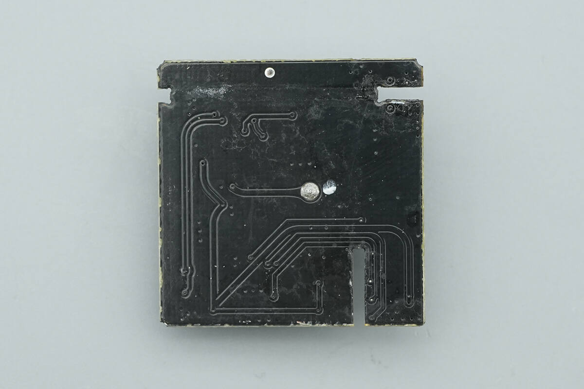
The back side has no components.
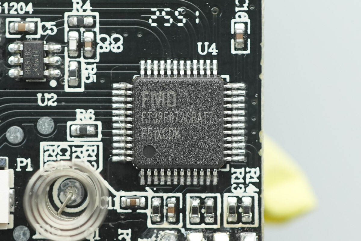
The MCU is from FMD, model FT32F072CBAT7. This MCU series uses the ARM® Cortex®-M0 32-bit RISC core, with a maximum operating frequency of 96MHz. It features high-speed memory, including up to 128k bytes of flash memory and 24k bytes of SRAM, as well as a wide range of enhanced I/O ports. The chip is packaged in an LQFP48 form factor.
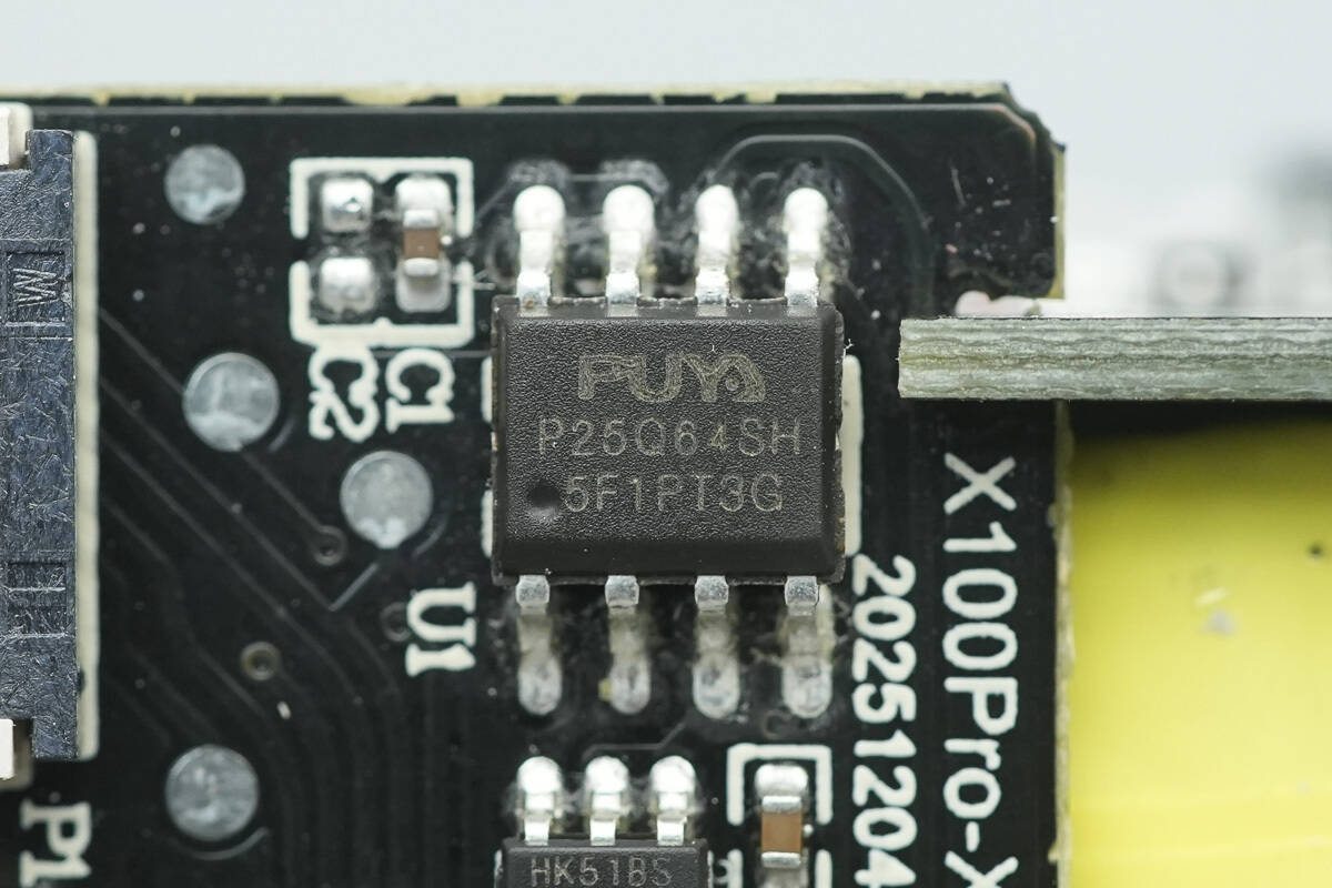
The external memory is from Puya, model P25Q64SH, with a capacity of 8MB, and is packaged in an SOP8 form factor.

The synchronous buck converter, marked with QKXx, is used for buck voltage conversion.
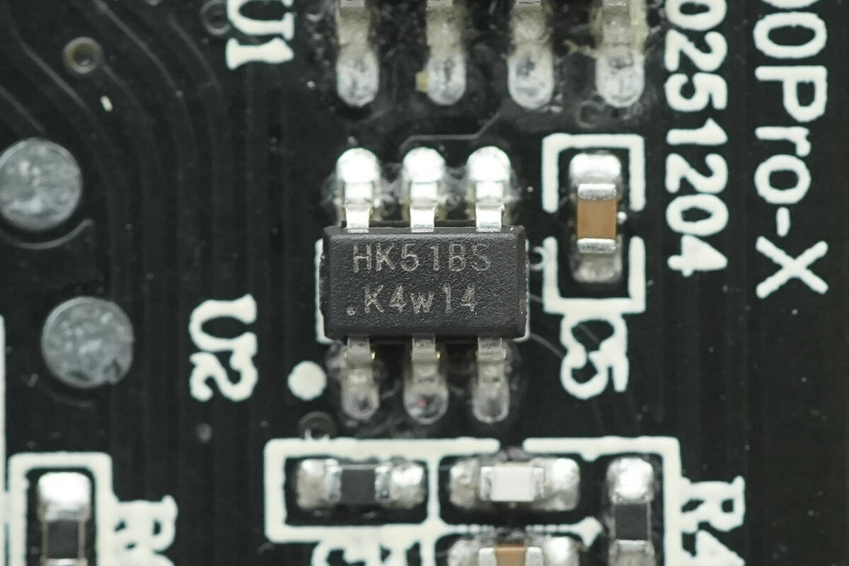
The touch detection chip, marked with HK51BS, is packaged in an SOT23-6 form factor.
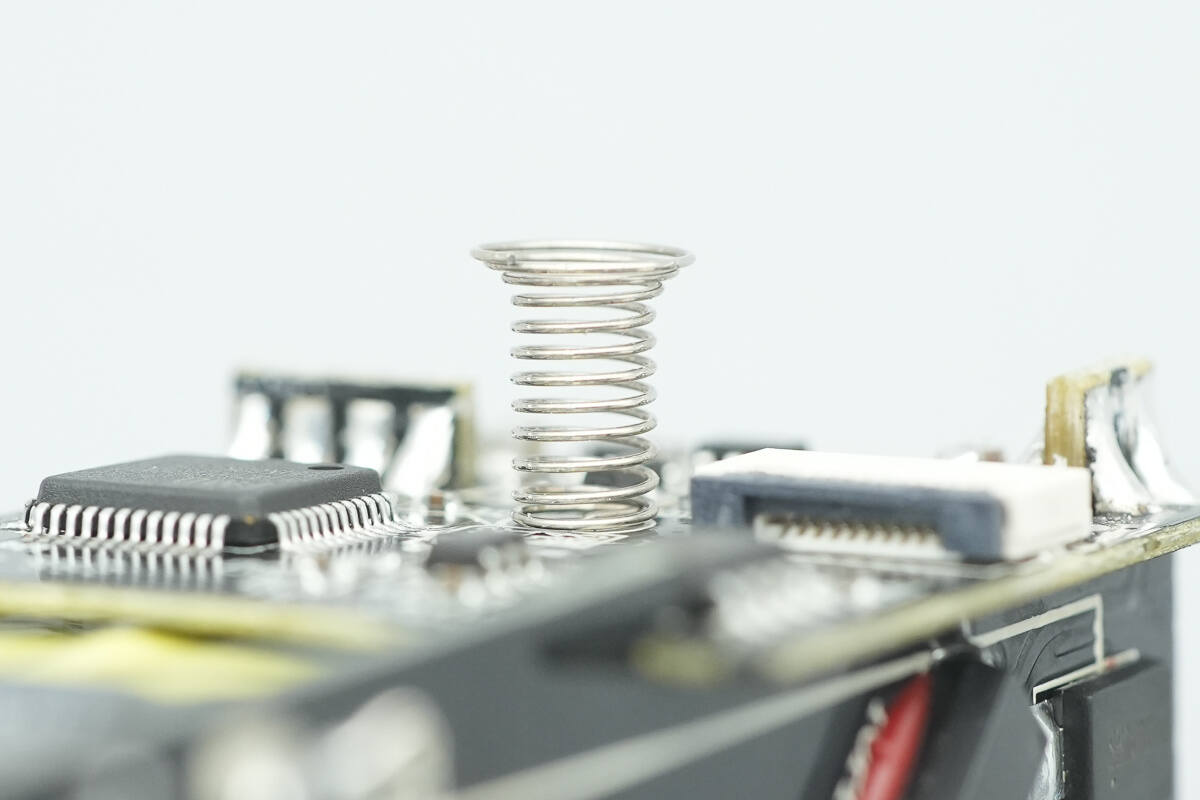
A close-up of the touch spring.
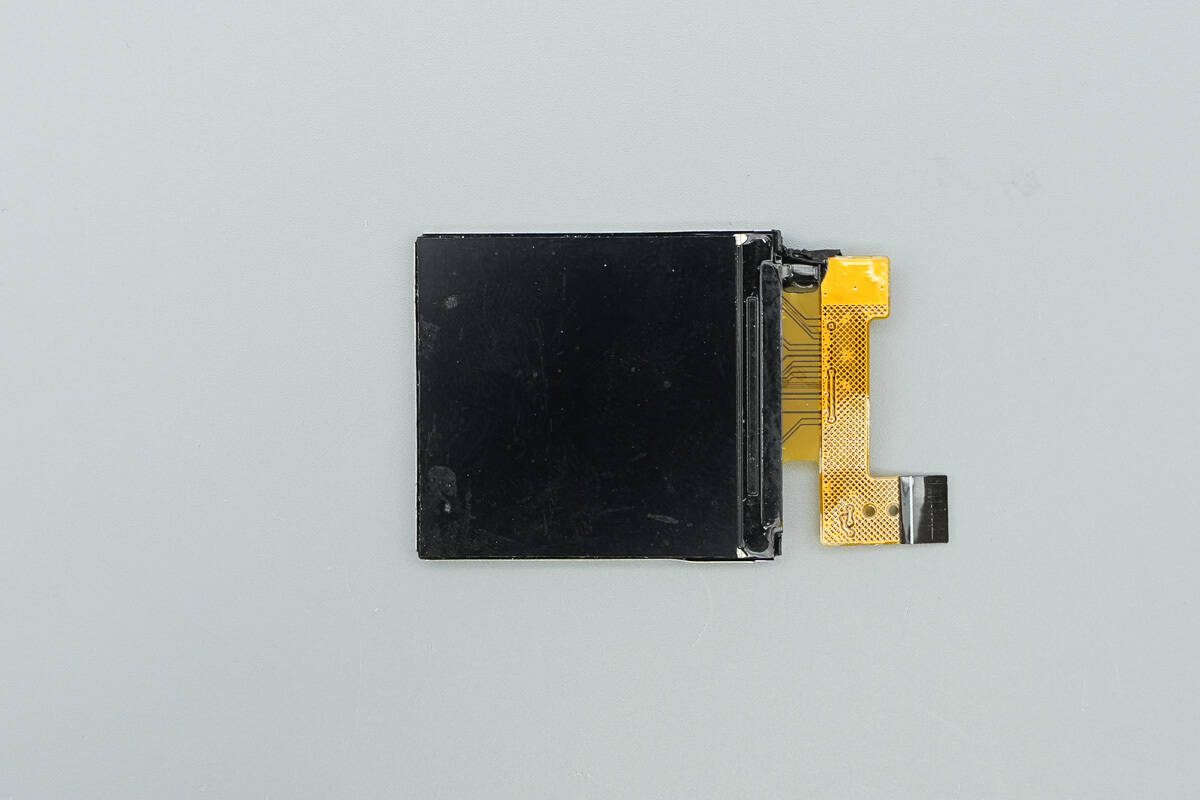
A close-up of the TFT color display.

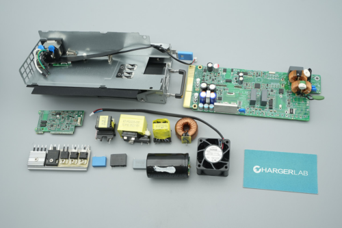
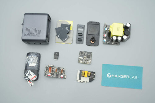
Well, those are all components of the VERYSUN 100W GaN Charger.
Summary of ChargerLAB
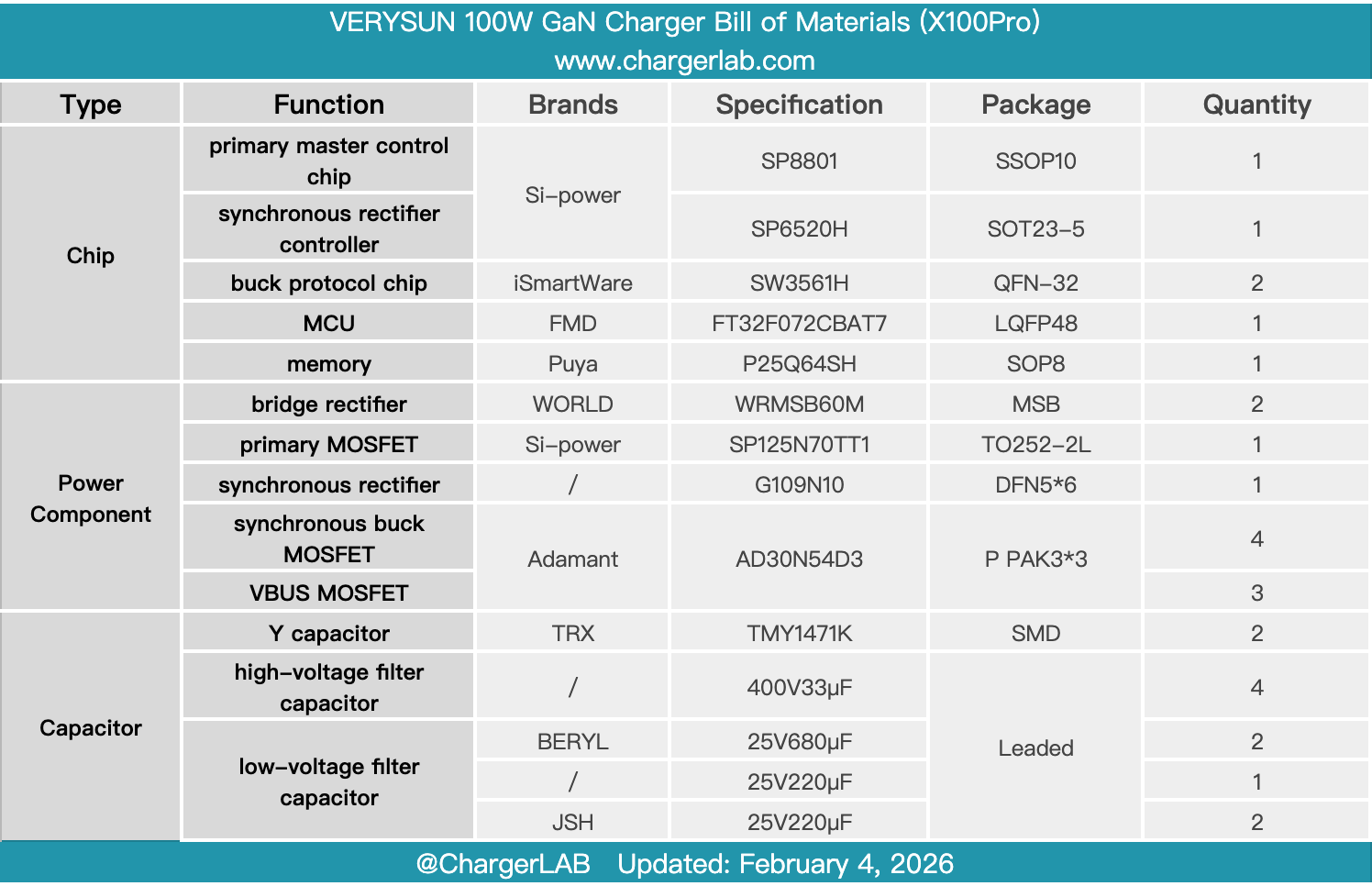
Here is the component list of the VERYSUN 100W GaN Charger for your convenience.
It is equipped with a TFT color screen that displays real-time power, temperature, and multi-port operating status. The charger features two USB-C ports and one USB-A port, supporting fast charging protocols such as PD3.2, PPS, and AVS. The support for the PD3.2 AVS voltage range, in particular, allows it to meet the fast charging needs of various devices.
After taking it apart, we found that it adopts a high-performance power solution using Si-Power SP8801 + SP6520H with a PFC-less switching capacitor, paired with the Si-Power SP125N70TT1 GaN FET. On the secondary side, two iSmartWare SW3561H buck protocol chips are used.
Internally, a large amount of adhesive is used, and heatsinks are applied to enhance heat dissipation, while a thermistor is included for temperature monitoring to ensure stability and safety under high load conditions. Notably, the successful mass production and application of Si-Power's power solution, which deeply integrates digital control with GaN power devices, marks a significant breakthrough in the high-end fast-charging power supply field. This solution provides a high-performance, high-reliability domestic technology option for the multi-port fast-charging market with power ratings of 100W and above.
Related Articles:
1. Teardown of Lenovo thinkplus FLUXO 150W GaN Desktop Charging Station (CSFO150A4)
2. Teardown of Momax 10000mAh Semi-Solid State Magnetic Power Bank (IP163Q22)
3. Teardown of Aohai Technology 3200W 80 PLUS Titanium Server Power Supply (AH-CRPS3200A1A)