Introduction
On June 5th, Nintendo launched the next-generation gaming console, the Switch 2, eight years after the release of its predecessor. With such a long gap, significant advancements in technology have been made, and as a result, the Switch 2 boasts substantial upgrades in hardware performance, display quality, and controller design.
Thanks to these improvements, the Switch 2 has seen impressive sales, selling over 3.5 million units in just four days. We got our hands on the new console as soon as possible for a review. The original charger supports up to 60W PD fast charging. Let’s take it apart to see its internal components and structure.
Product Appearance
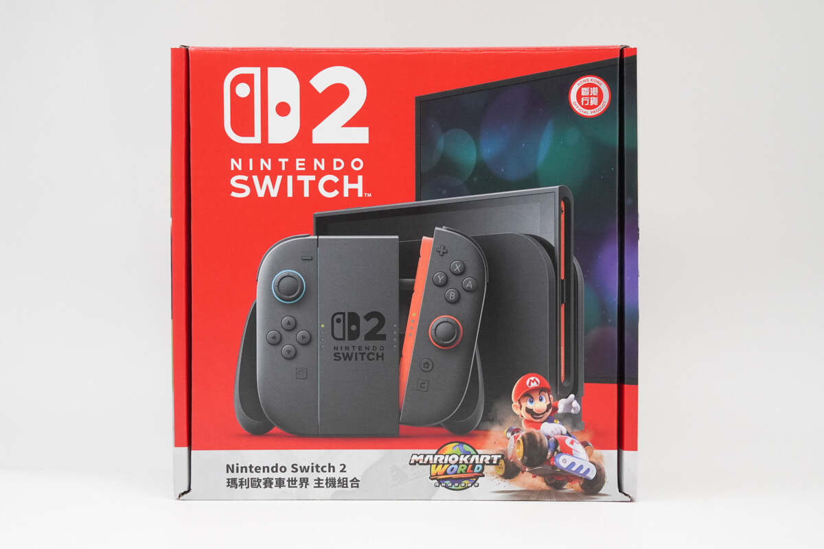
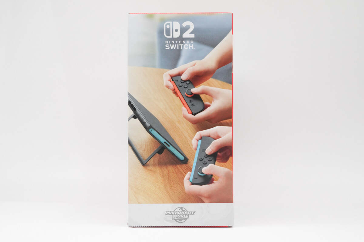
The packaging continues the classic red theme, with the front featuring images of the product itself as well as elements from Mario Kart and other related graphics.
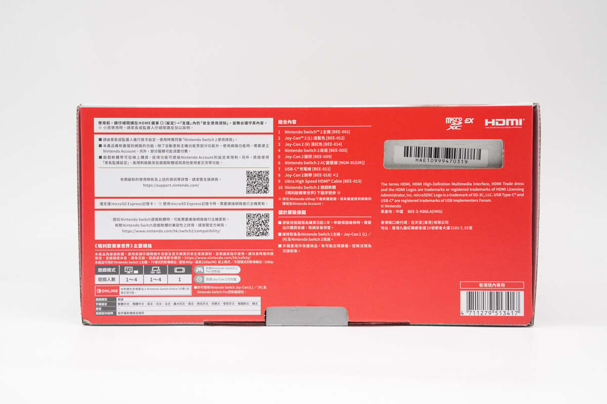
The packing list and precautions are printed on the side.
The other side is printed with product usage scenarios.
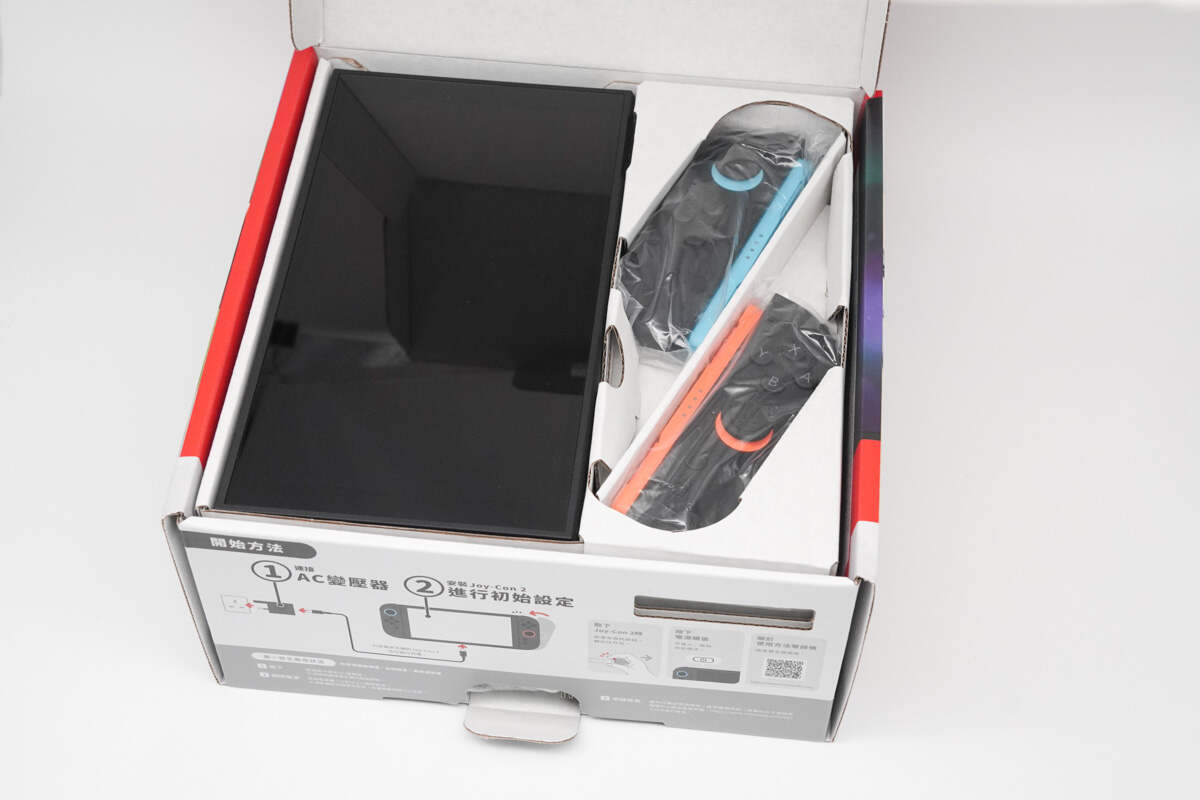
The Nintendo Switch 2 is secured with cardboard.
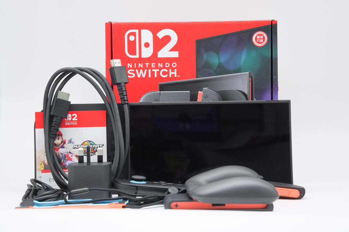
The package includes the Switch 2 console, Joy-Con set, dock, charger kit, HDMI cable, and more.
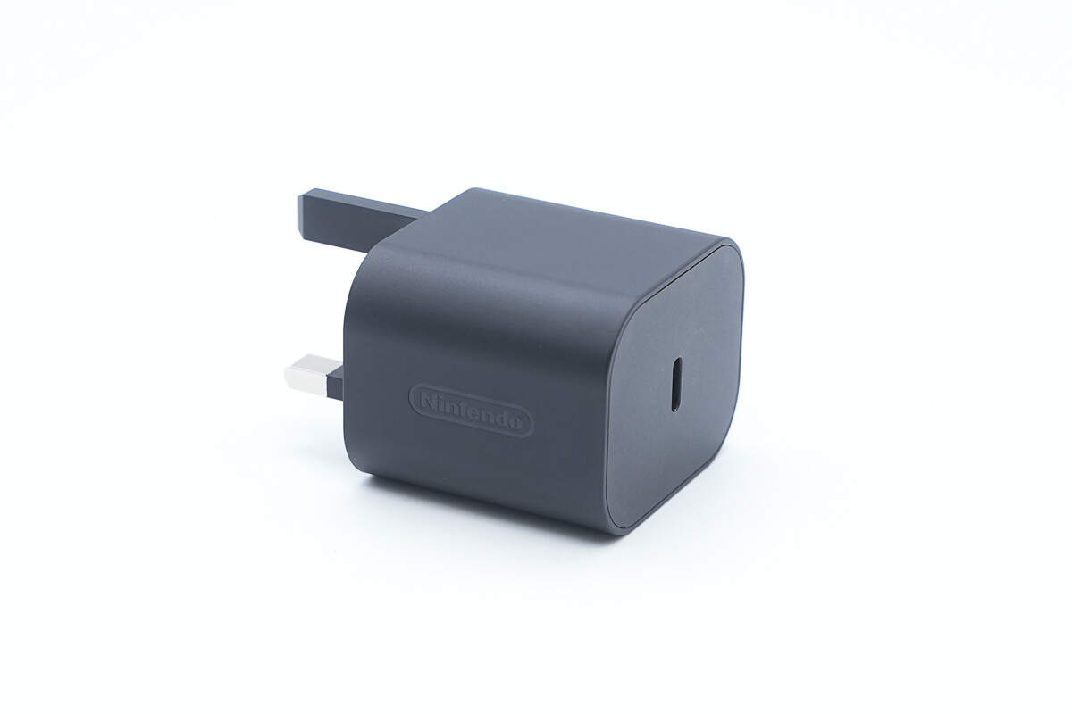
The charger is made of flame-retardant PC material, with a frosted surface and rounded edges on both sides.
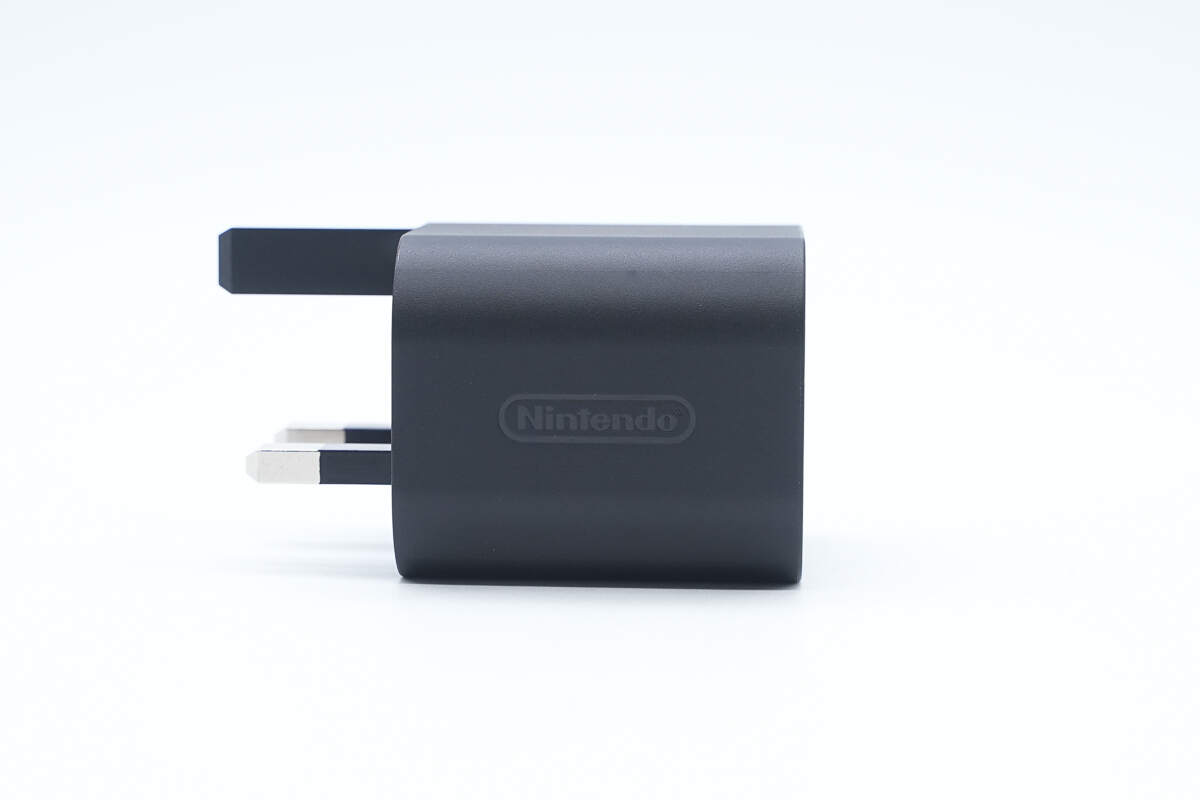
There is a Nintendo logo on one side.
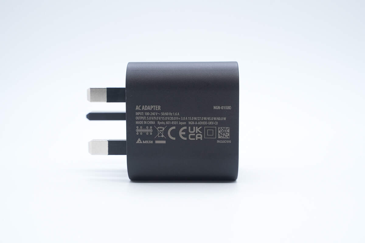
The spec info is printed on the back.
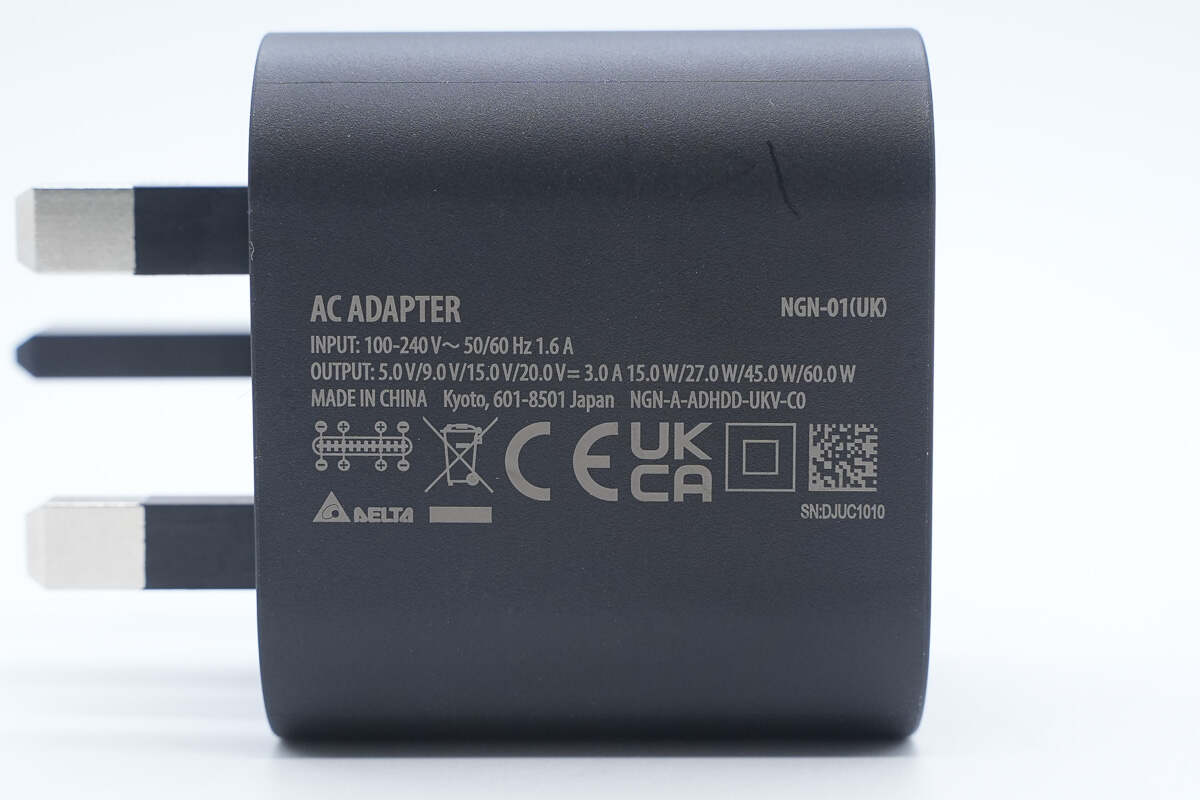
Input: 100-240V~50/60Hz 1.6A
Output: 5/9/15/20V3A 60W Max
Manufacturer: Delta Electronics Co., Ltd.
It is CE, UKCA certified.
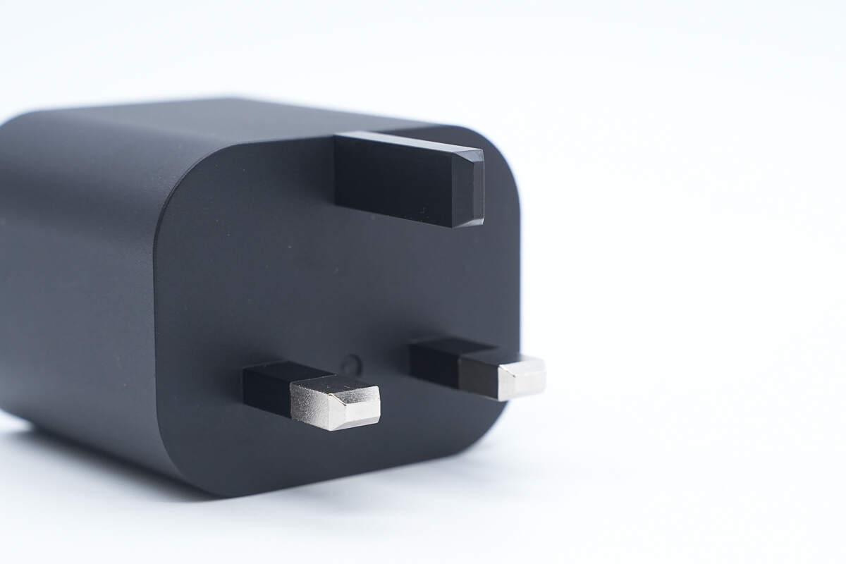
The input end is equipped with a UK plug.
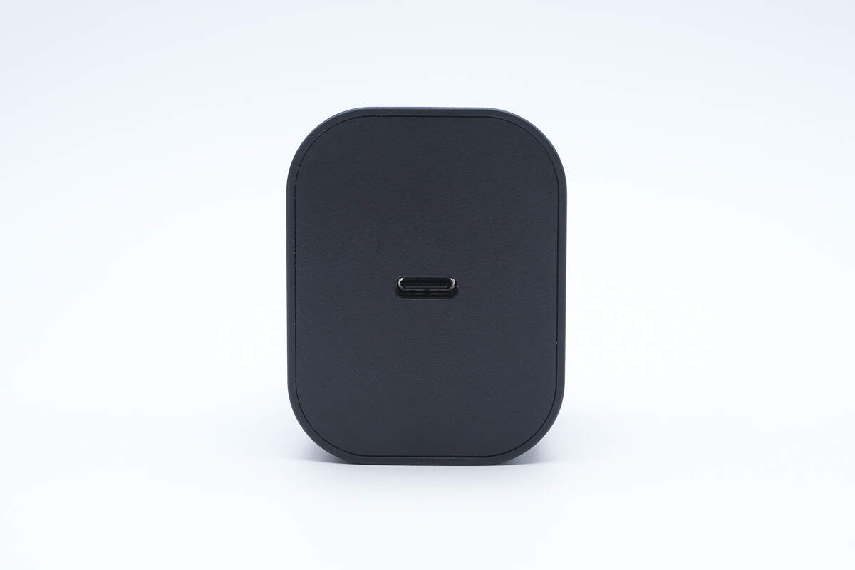
The output end is equipped with a USB-C port.
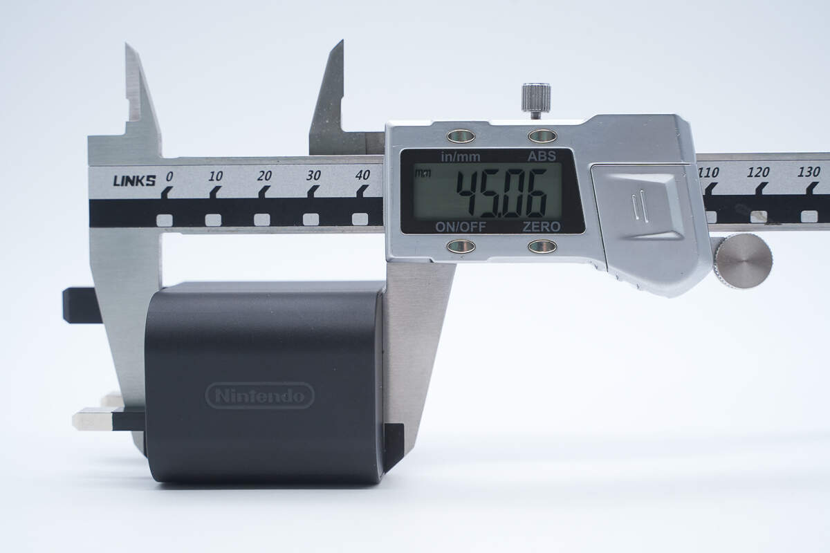
The length is about 45.06 mm (1.77 inches).
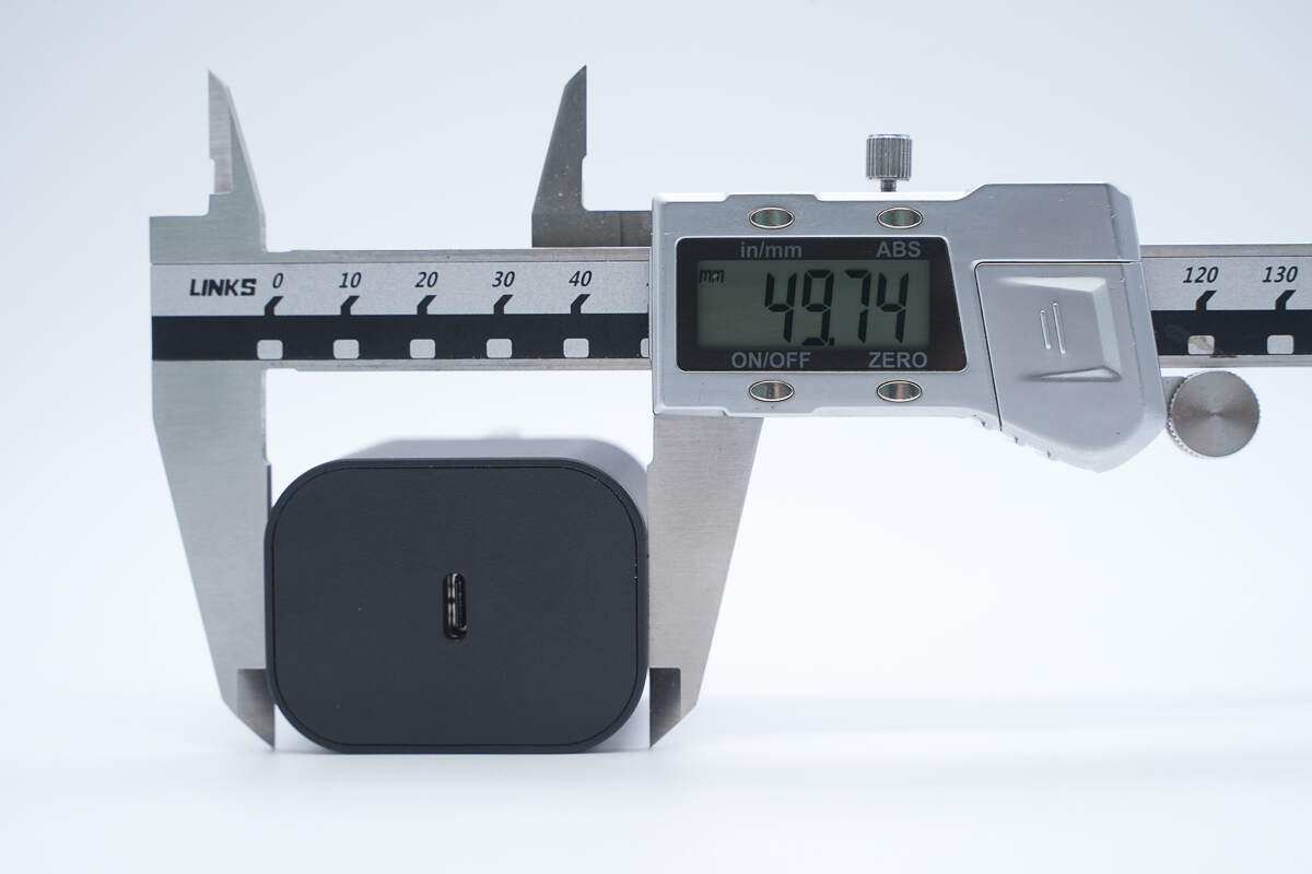
The width is about 49.74 mm (1.96 inches).
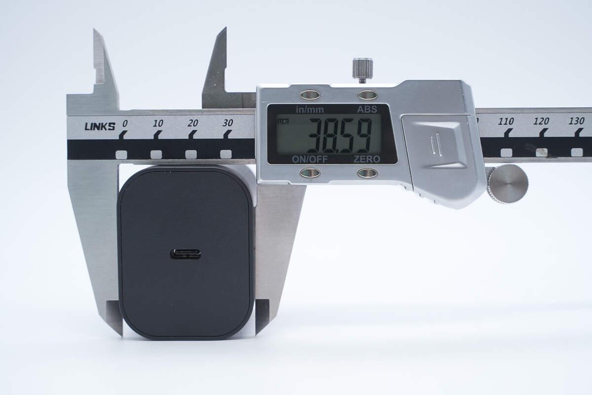
The thickness is about 38.59 mm (1.52 inches).
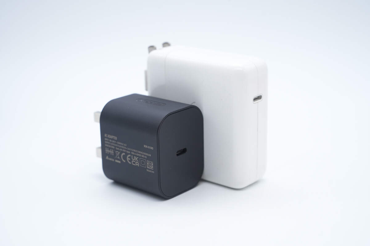
It is significantly smaller than the Apple 61W charger.
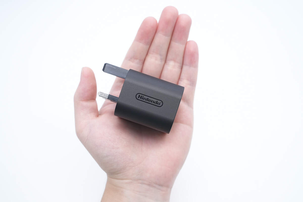
That's how big it is in the hand.
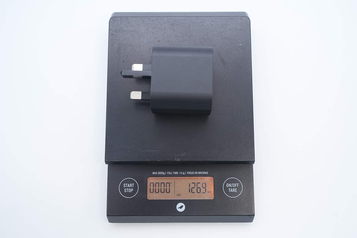
The weight is about 127 g (4.48 oz).
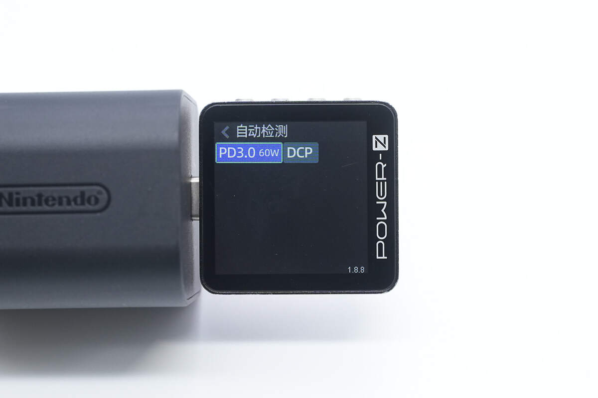
ChargerLAB POWER-Z KM003C shows it supports PD3.0 and DCP protocols.
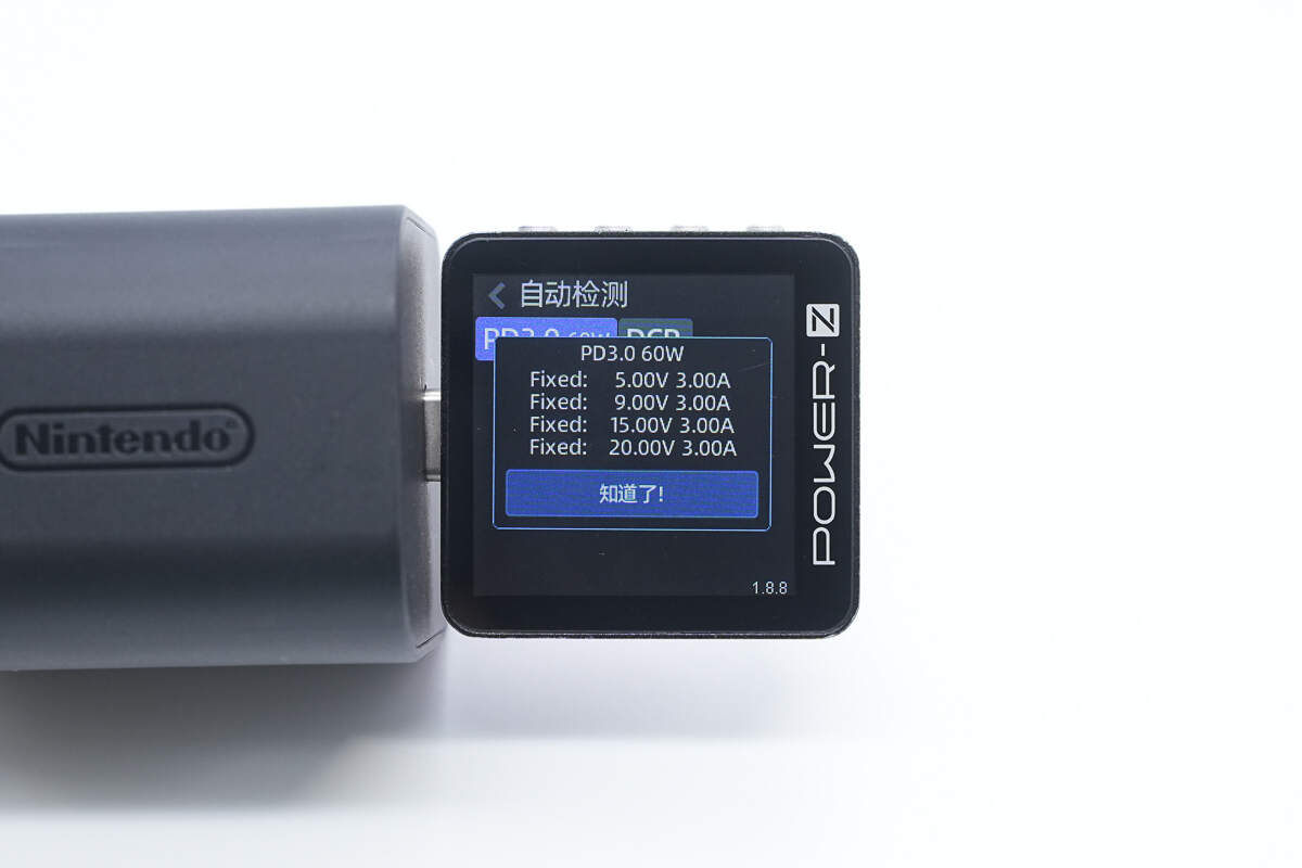
It has four fixed PDOs of 5V3A, 9V3A, 15V3A, and 20V3A.
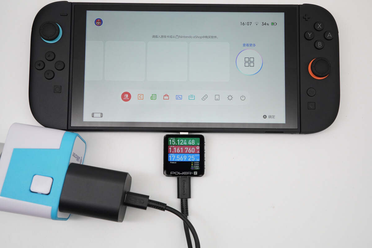
Using it to charge the Switch 2, the power is about 17.57W.
Teardown
Next, let's take it apart to see its internal components and structure.
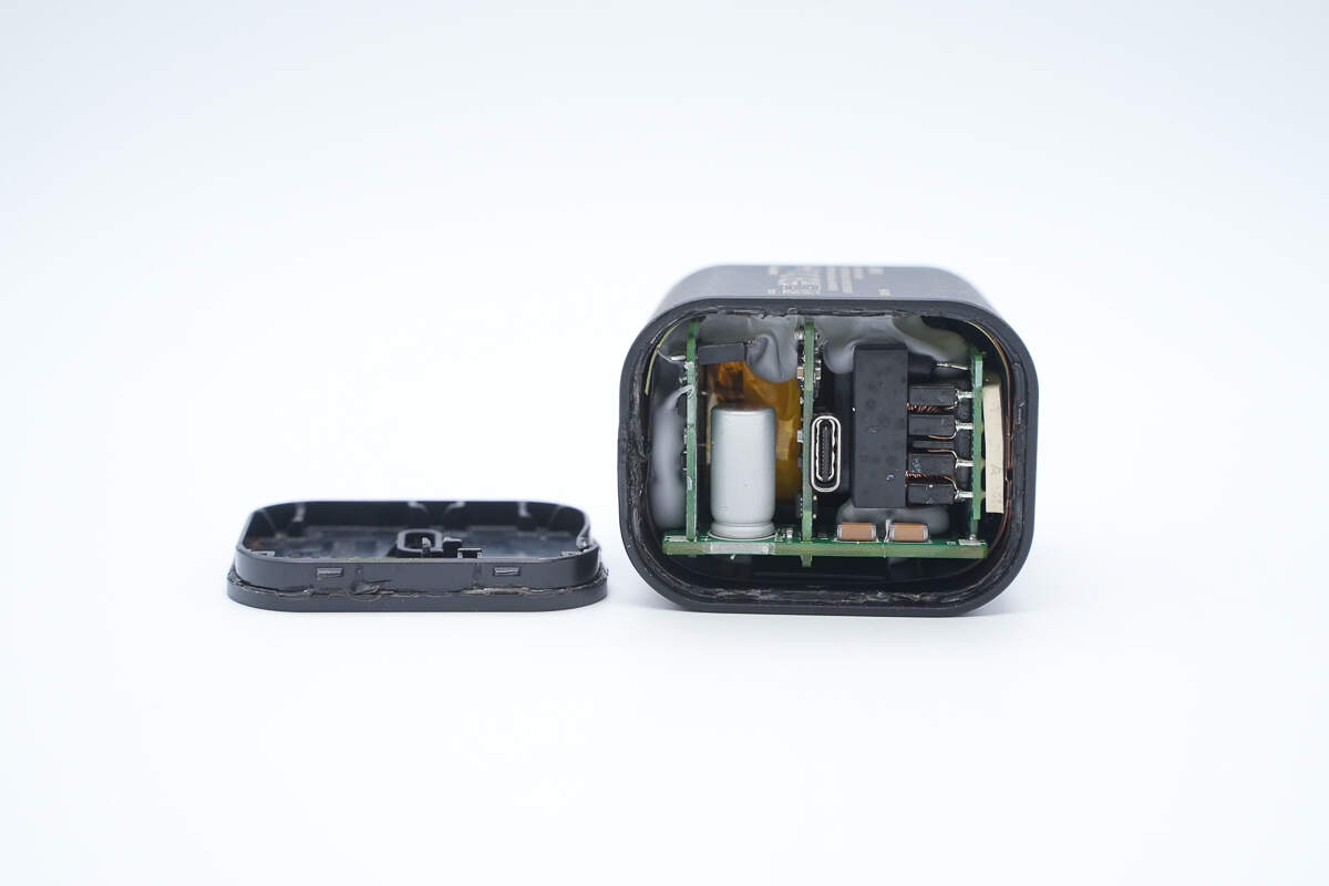
Cut open the top cover, it is secured with ultrasonic welding.
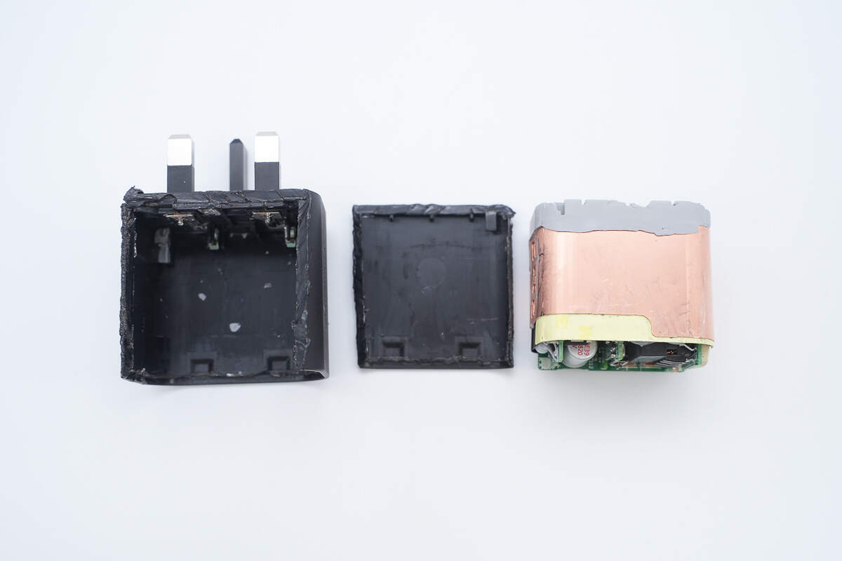
The PCBA module is fixed firmly and can only be removed by cutting the case.
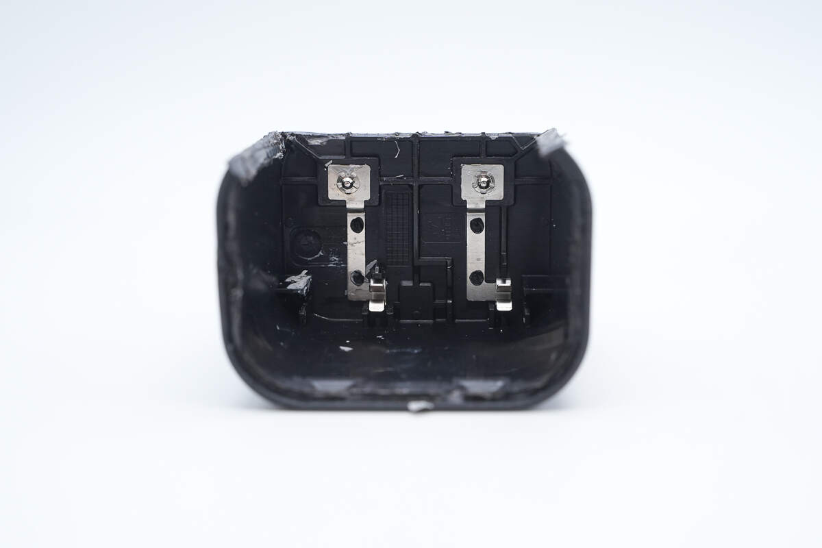
The input terminal uses a contact design for power supply.
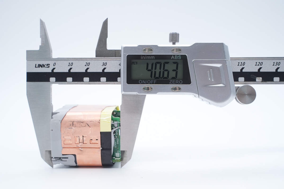
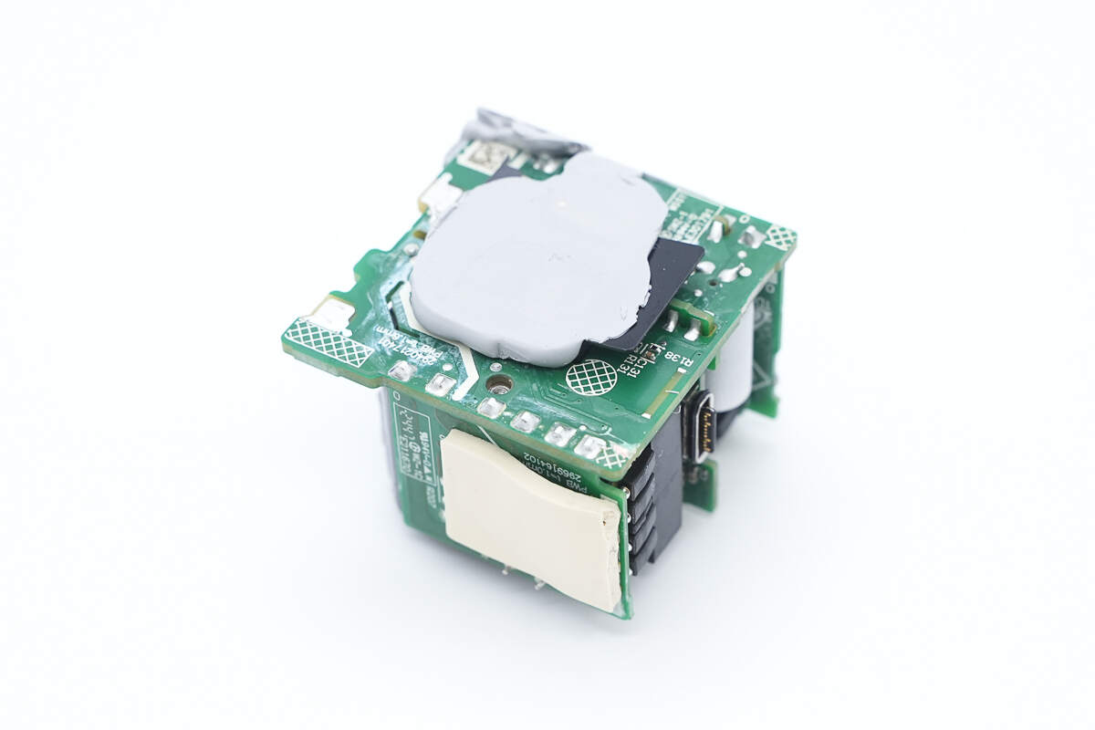
The length of the PCBA module is about 40.63 mm (1.6 inches).
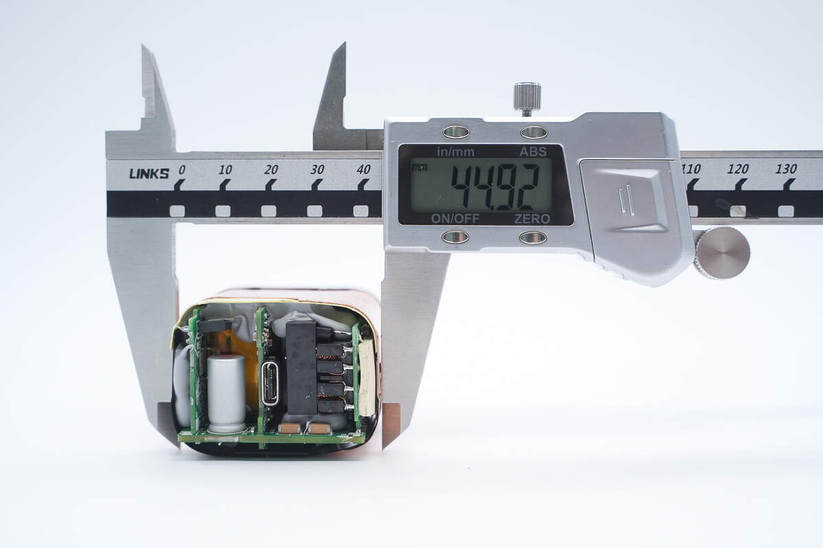
The width is about 44.92 mm (1.77 inches).
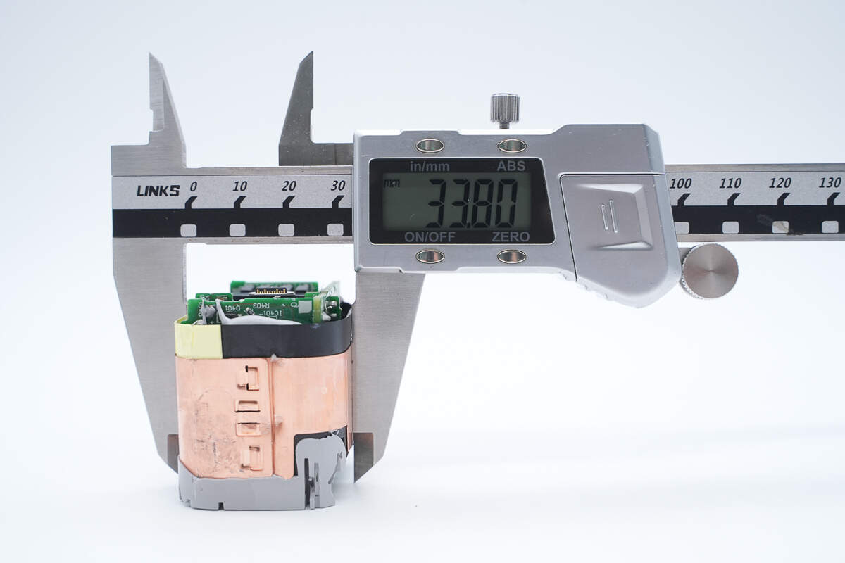
The thickness is about 33.8 mm (1.33 inches).
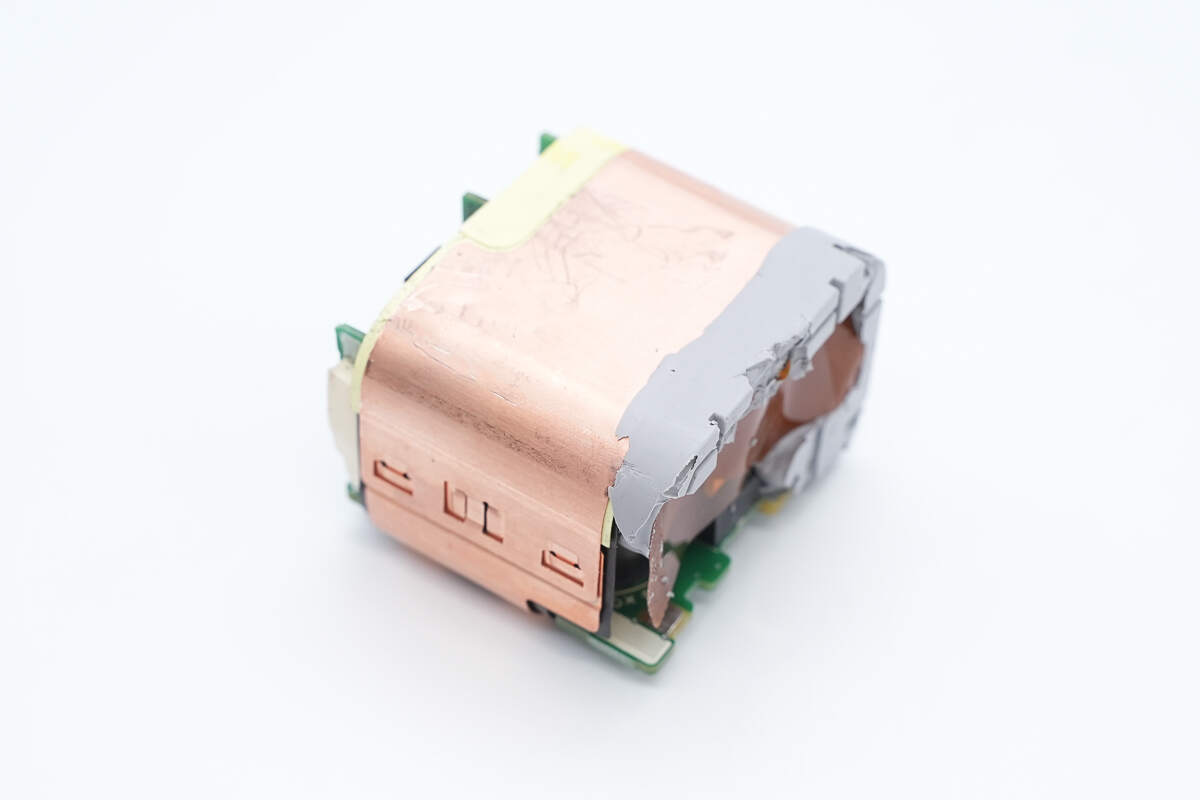
The PCBA module is wrapped in copper heat sinks and secured with a snap-on structure. The input end is glued and a high-temperature resistant insulation sheet is attached.
The copper heat sink is also fixed with screws and has Mylar sheets on the inside for insulation.
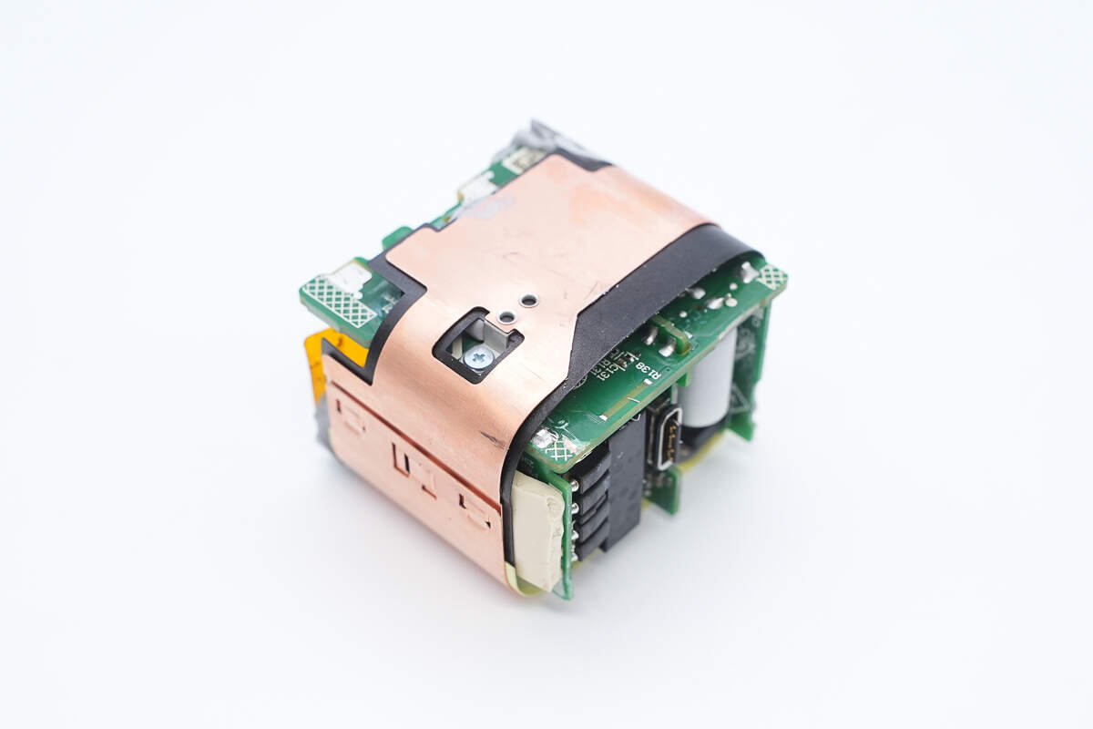
Remove the heat sink, the module is filled with potting compound, and the small PCB on the side is attached with a thermal pad.
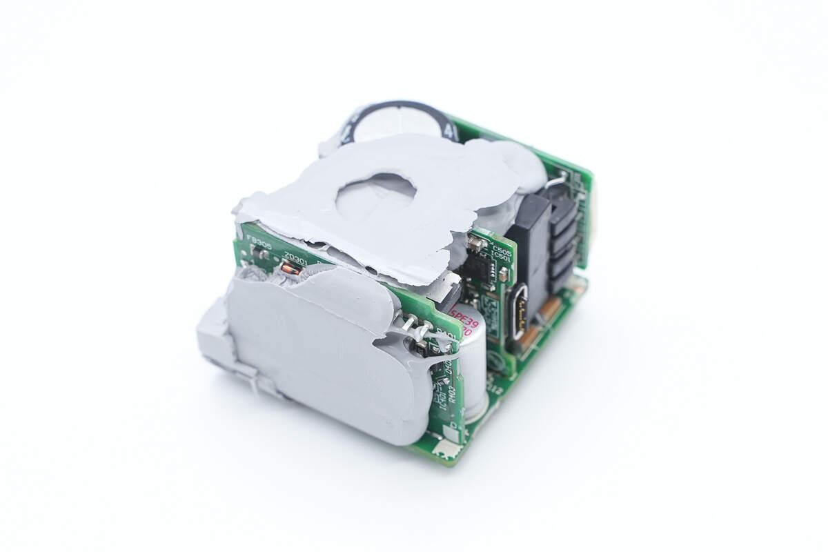
The other side is also filled with potting compound.
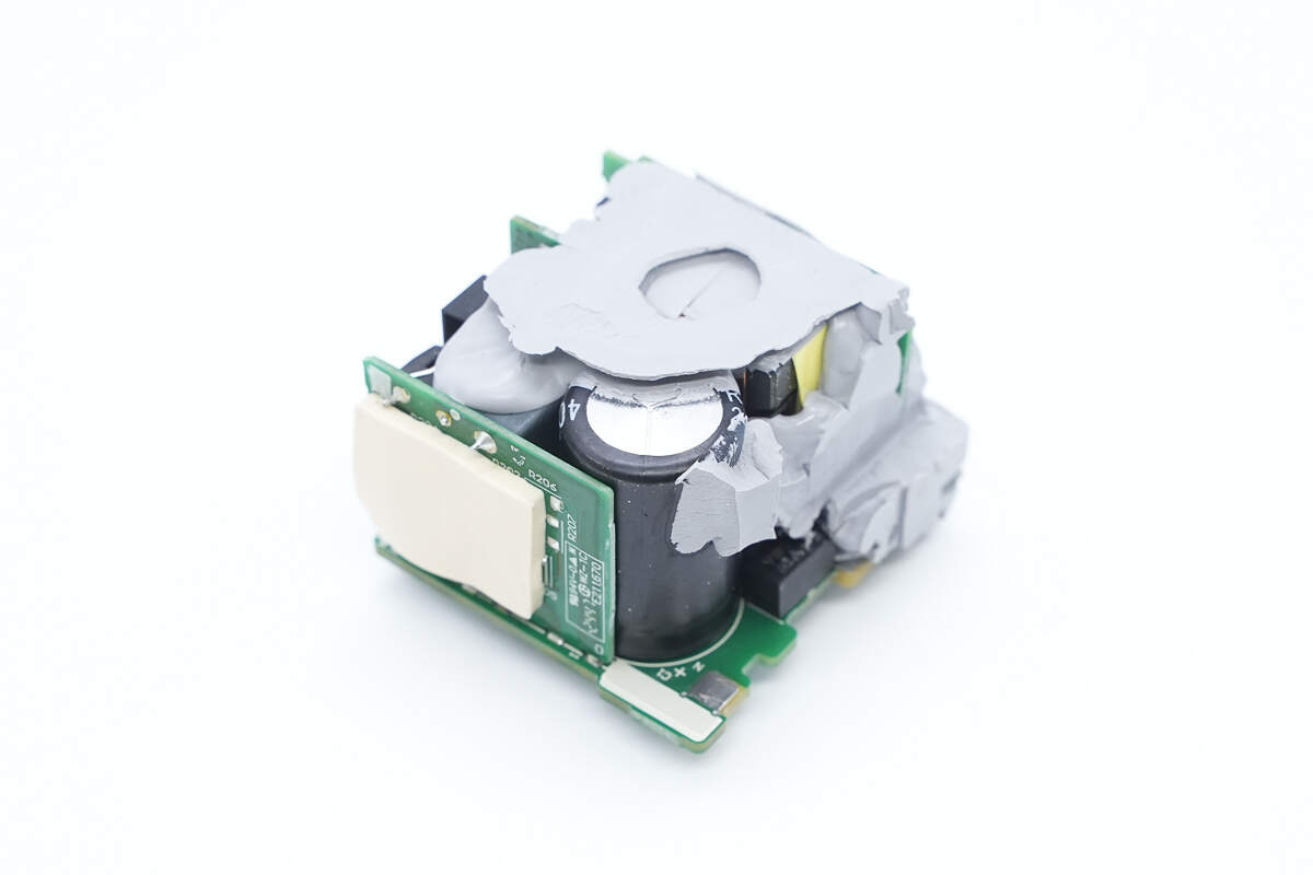
The mainboard's back side also has potting compound in the center, with Mylar film used for insulation between the primary and secondary sides.
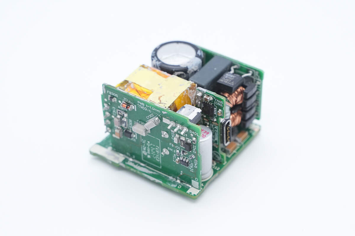
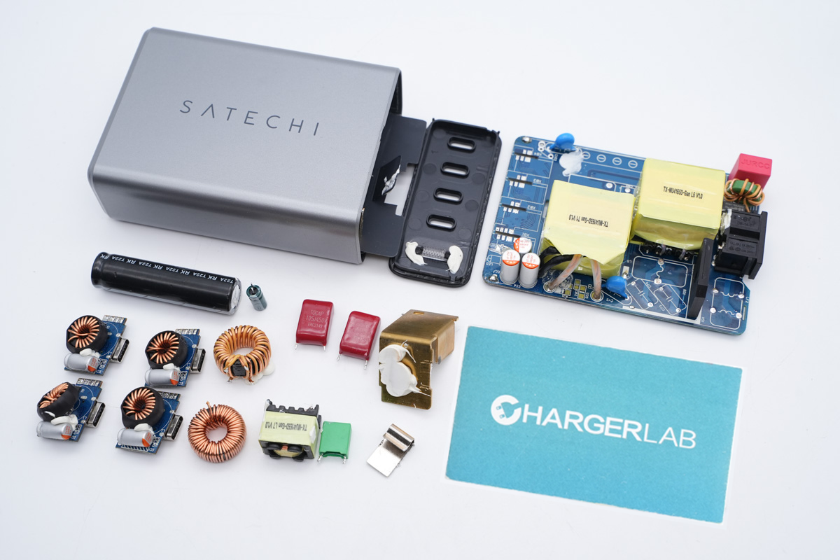
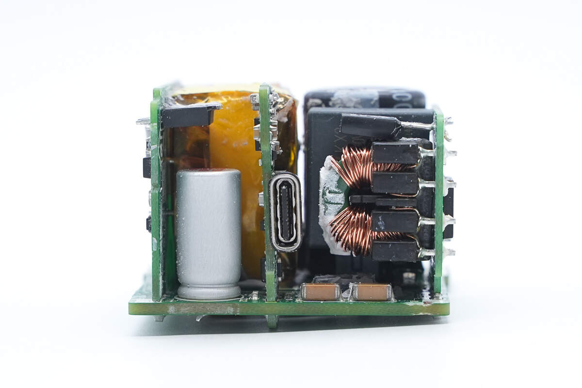
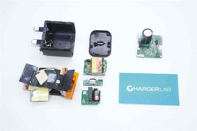
Clean off the potting compound. The PCBA module uses a design of stacking multiple small PCBs to make full use of the space.
The area between the small PCBs on both sides houses components such as a electrolytic capacitor and a transformer.
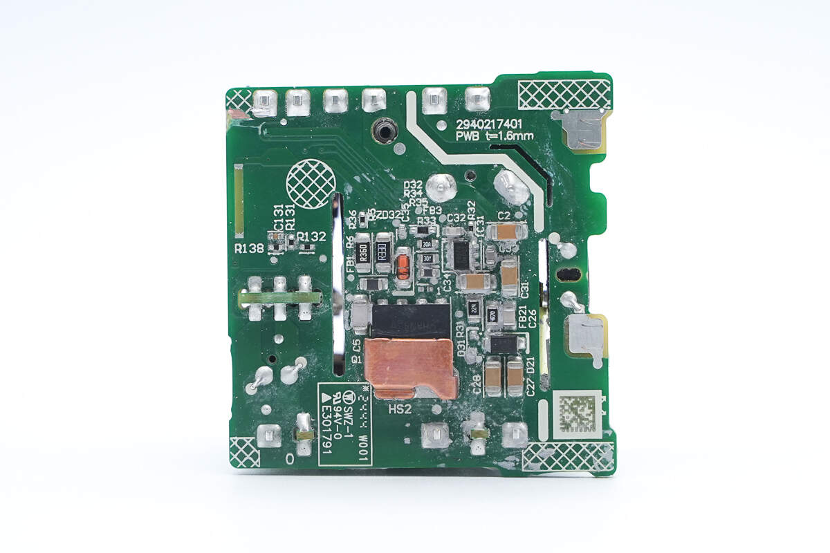
The back side has a master control chip and primary MOSFET, and the MOSFET is covered with a copper heat sink.
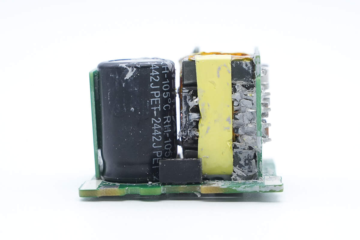
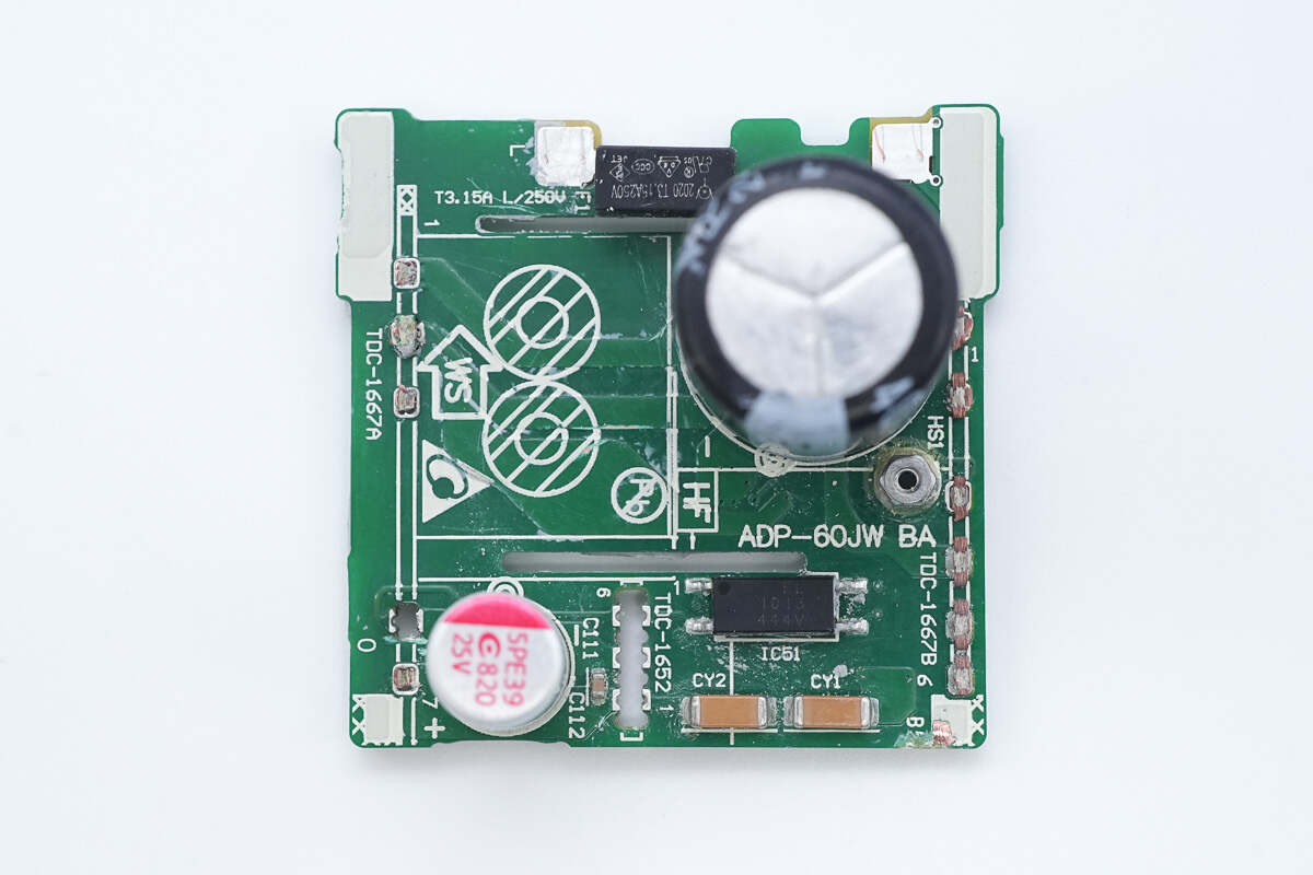
The input end has a time-delay fuse and an electrolytic capacitor.
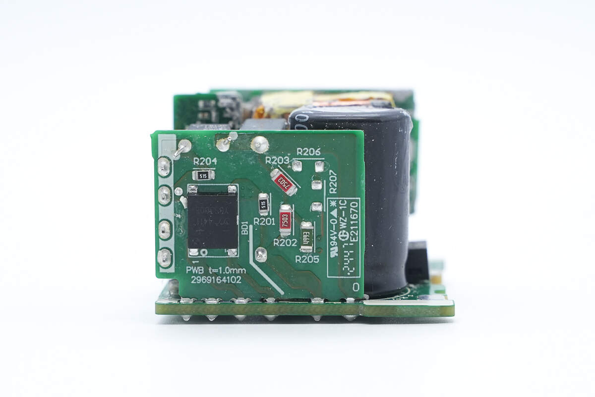
There is a bridge rectifier on the small PCB on the side.
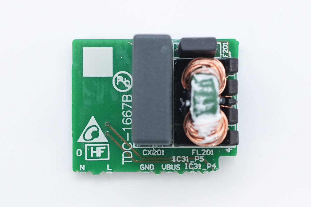
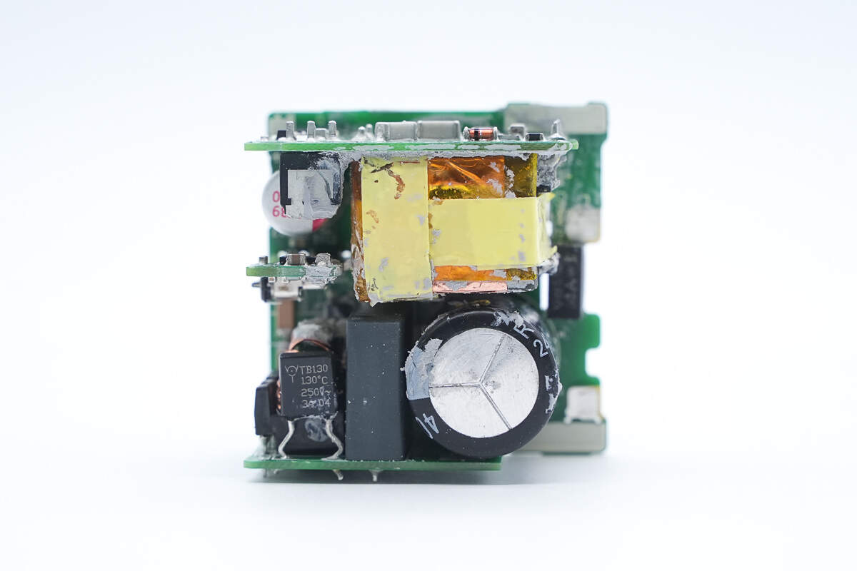
Remove the small PCB, there's a common mode choke, an X2 safety capacitor, and a thermal fuse on the other side.
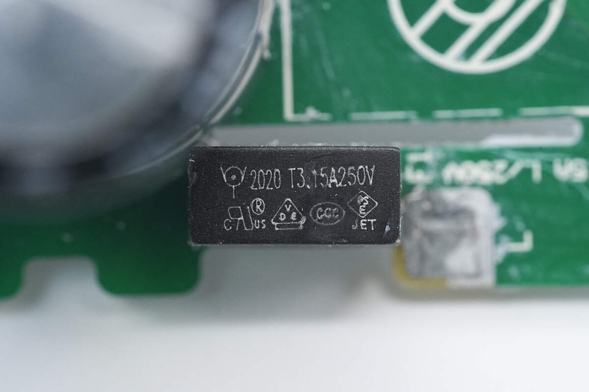
The time-delay fuse is from WalterFuse. 3.15A 250V.
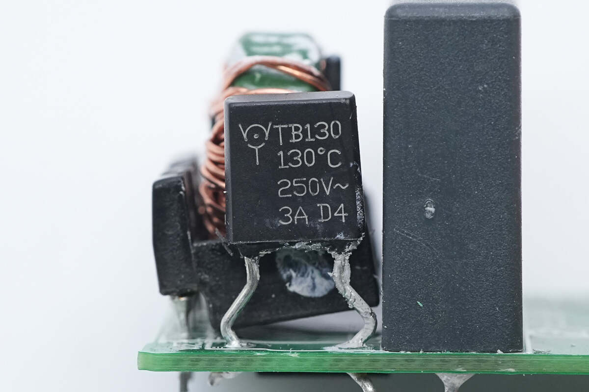
The thermal fuse is also from WalterFuse.
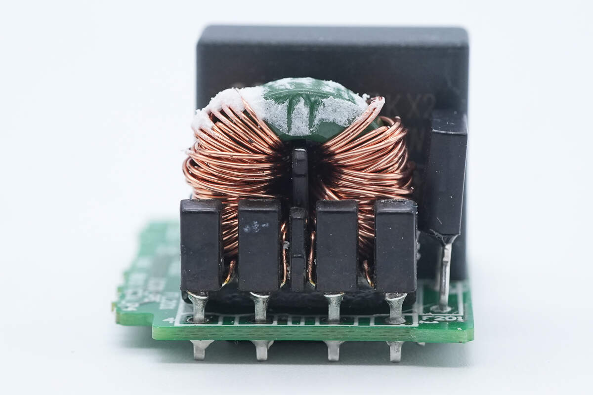
The common mode choke is used to filter out EMI interference.
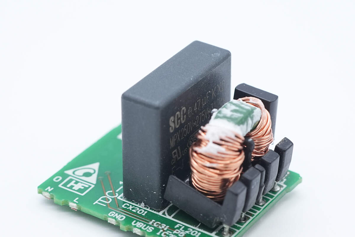
The safety X2 capacitor is from SCC. 0.47μF.
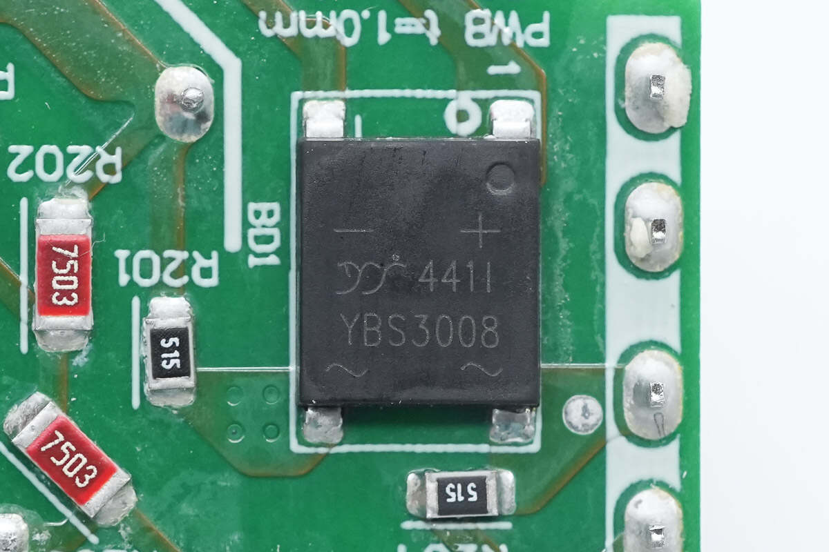
The bridge rectifier is from YJ and adopts the YBS package. 3A 800V. Model is YBS3008.
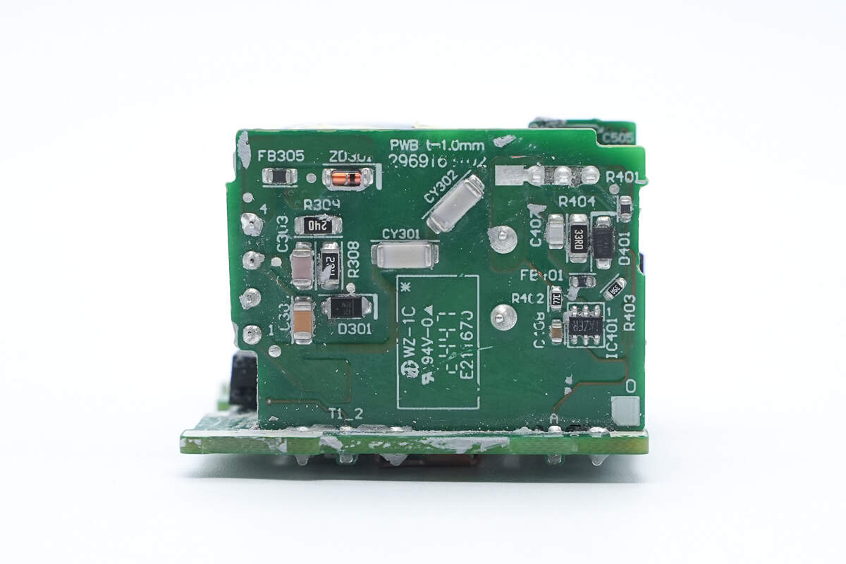
There is a synchronous rectifier controller on the back of the small PCB on the other side.
Remove the small PCB, there is a transformer and a synchronous rectifier on the other side.
After removing all the small PCBs, the front of the mainboard is equipped with an optocoupler, SMD Y capacitor and a solid capacitor for output filtering.
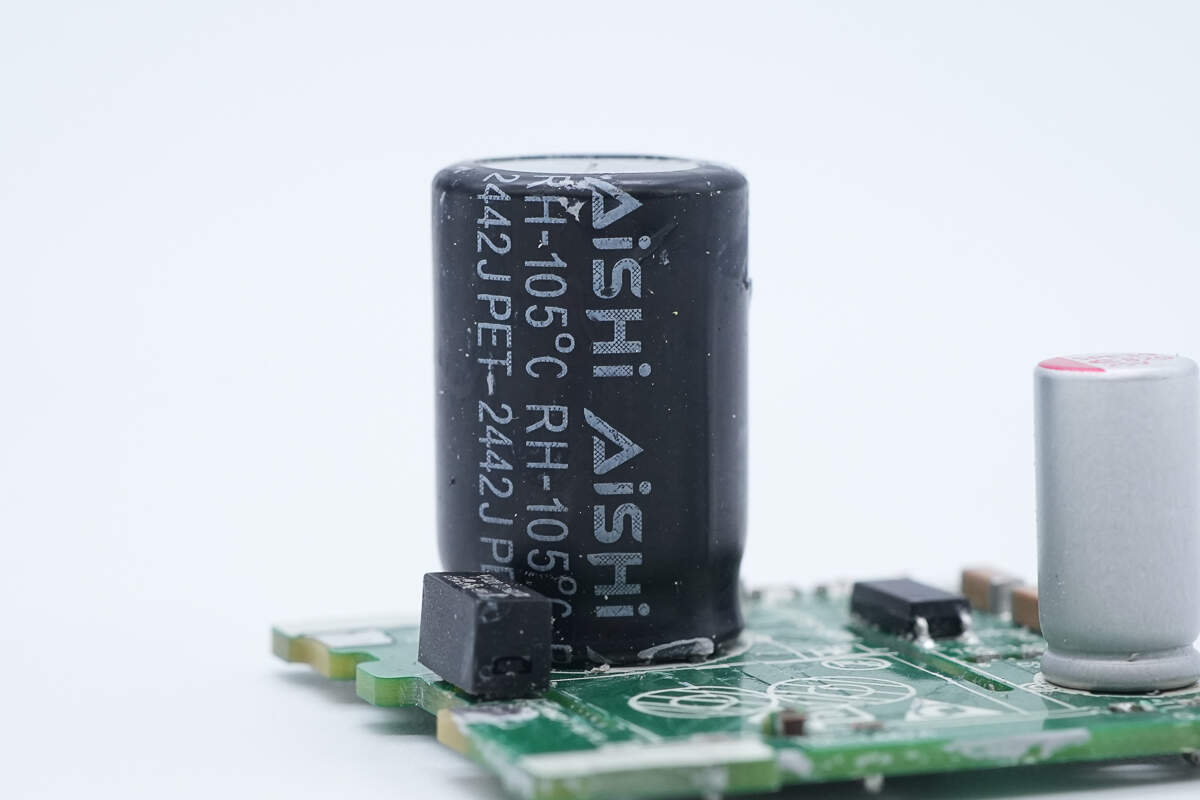
The electrolytic capacitor is from AiSHi.
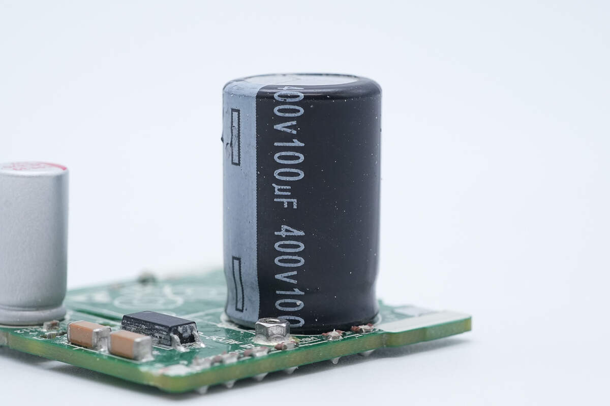
The specification is 400V 100μF.
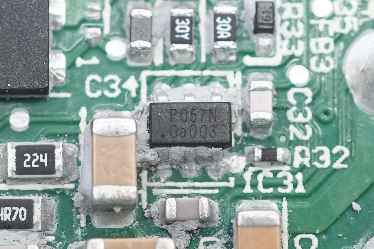
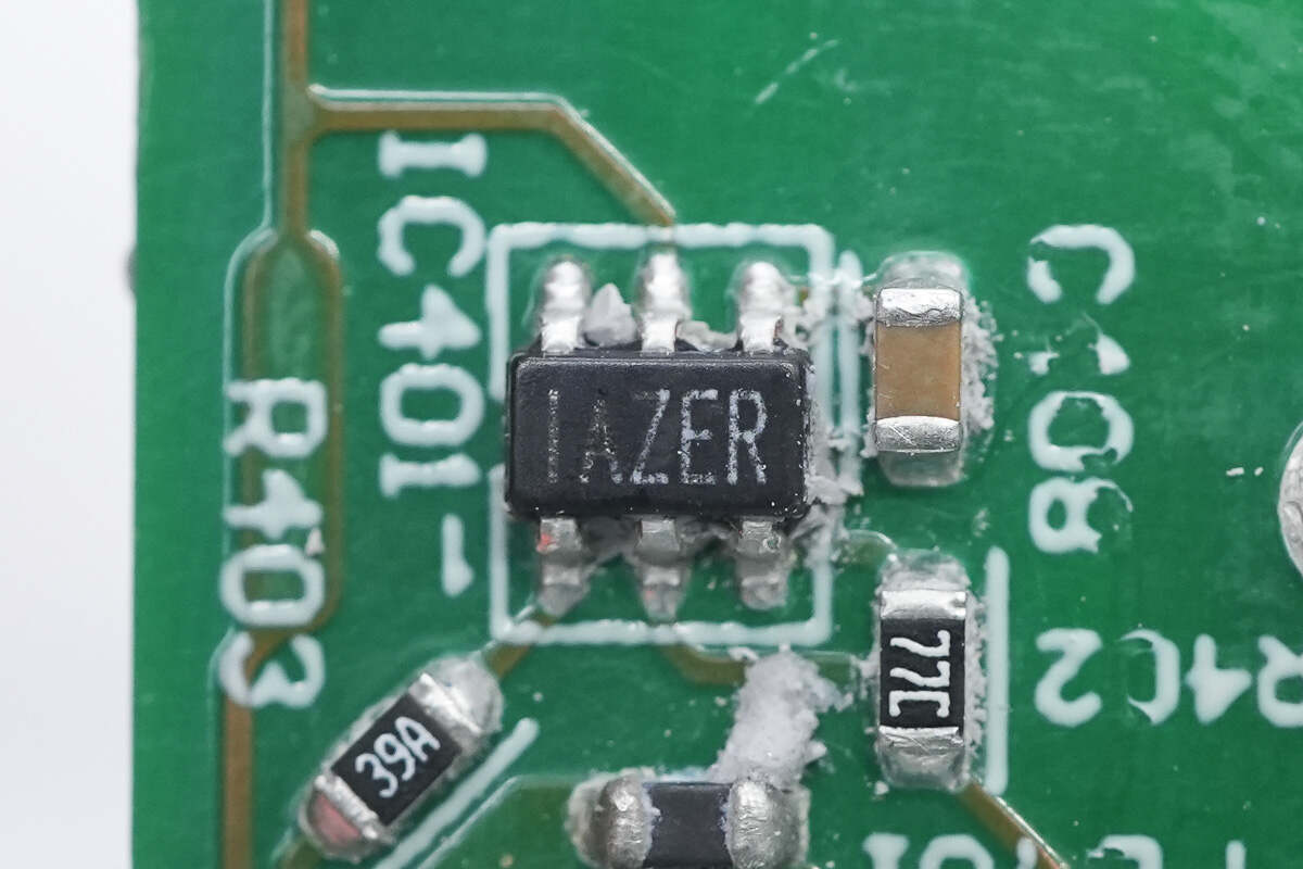
The master control chip is marked with P057N and adopts the SOT23-6 package.
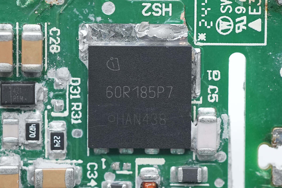
The primary MOSFET is from Infineon, belonging to the CoolMOS P7 series. It adopts the PG-VSON-4 package. 650V 185mΩ. Model is IPL60R185P7.
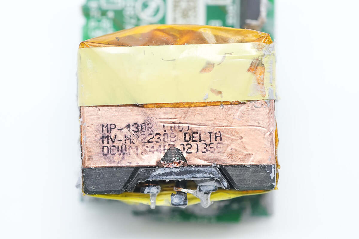
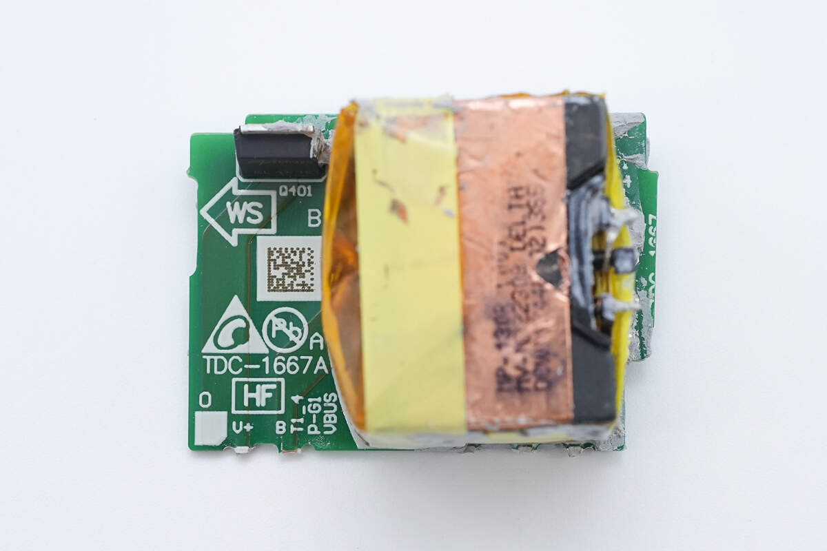
The transformer is wrapped with copper foil and insulating tape.
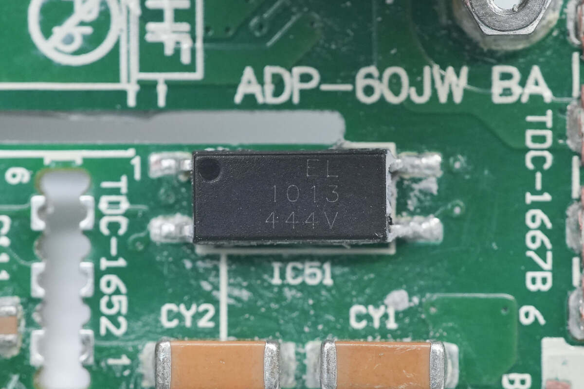
The Everlight EL 1013 optocoupler is used for output voltage feedback.
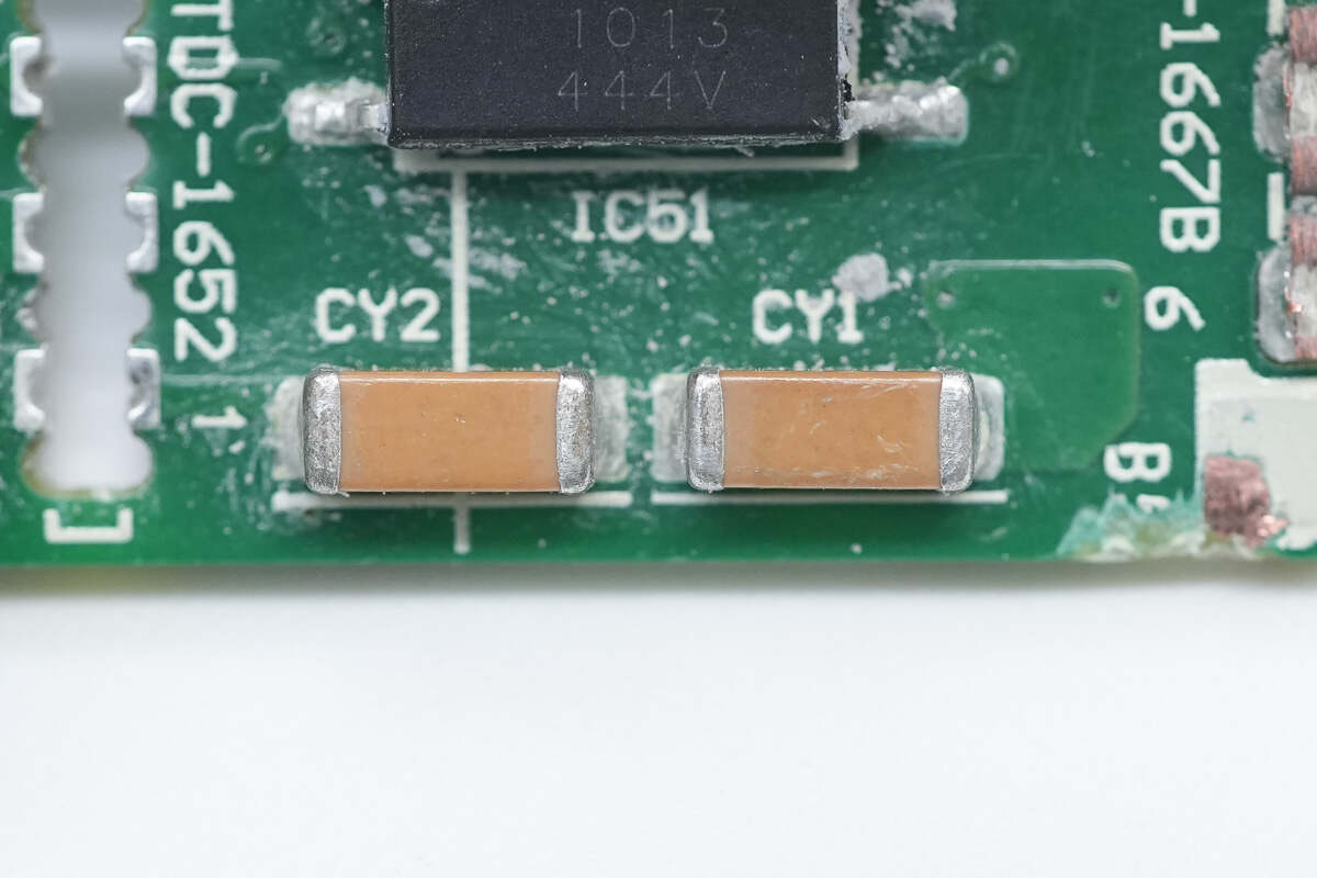
The two SMD Y capacitors next to it are connected in series to increase the withstand voltage rating.
The synchronous rectifier controller is from MPS. It supports a wide output voltage range, supports DCM/CCM/quasi-resonant operation modes, and supports high-side and low-side synchronous rectification. Model is MP6908
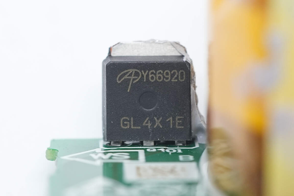
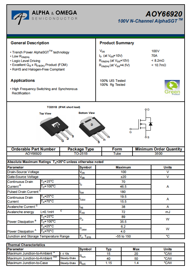
The synchronous rectifier is from AOS and adopts the TO251B package. 100V 8.2mΩ. Model is AOY66920.
There is the information about the AOS AOY66920.
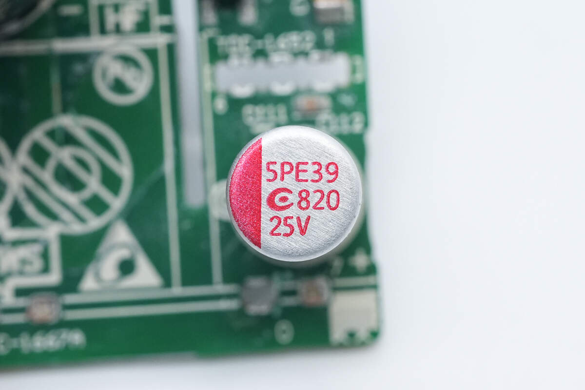
The solid capacitor for output filtering is from APAQ. 25V 820μF.
The output end has a small PCB with a USB-C port soldered in the center.
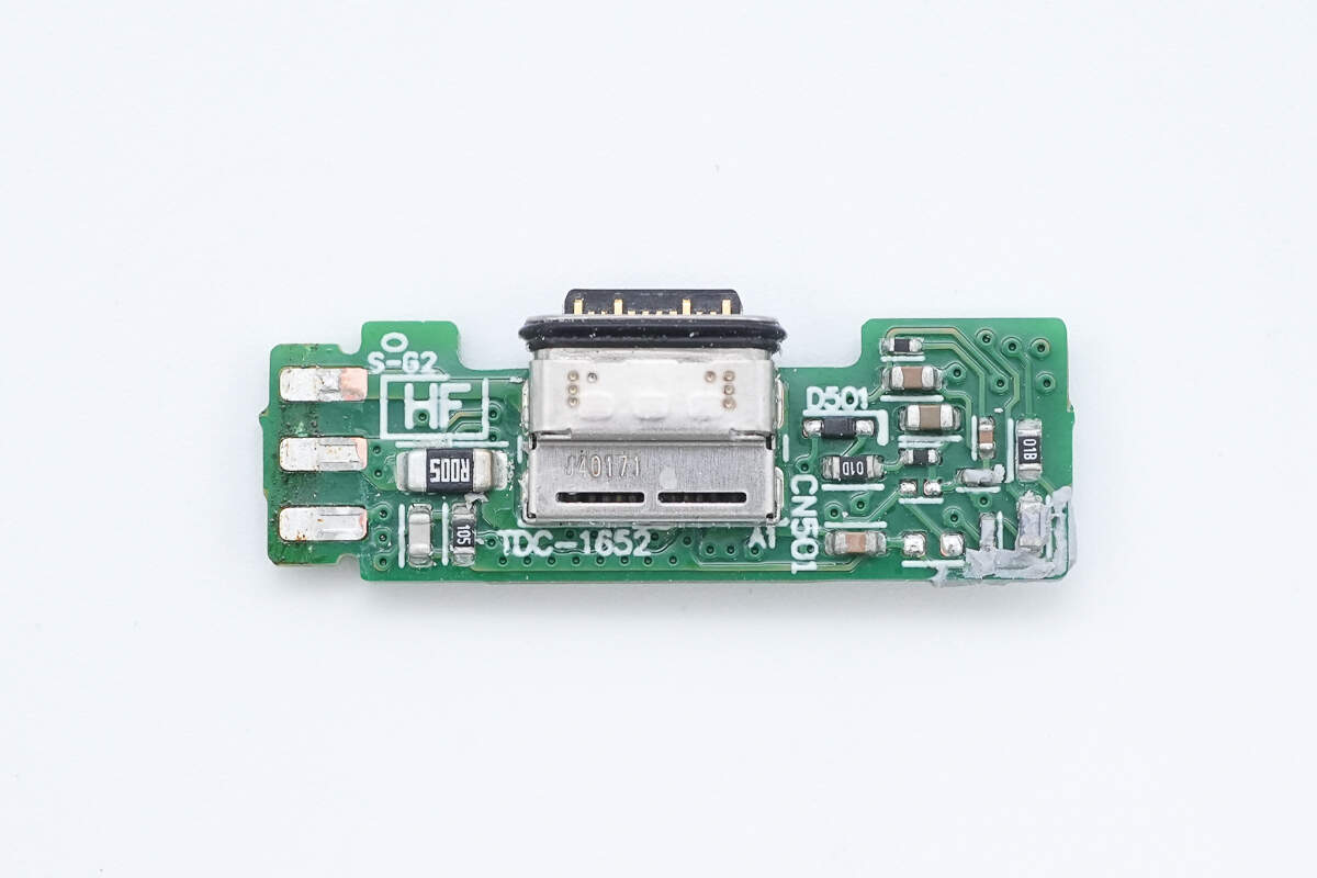
The USB-C socket is soldered on the front of the small PCB.
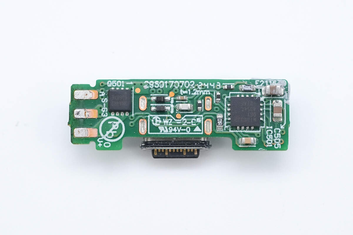
There is a protocol chip and output VBUS MOSFET on the back.
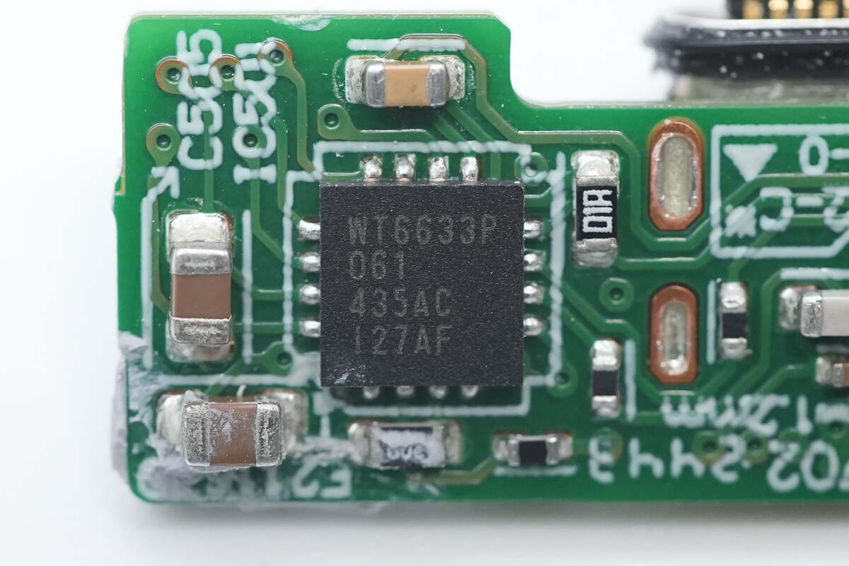
The protocol chip is from Weltrend. It supports USB PD3.0, Qualcomm QC4, QC4+ and QC5. It has passed USB-IF certification, TID1070018. It has also passed Qualcomm QC5 certification, certification number 4789627043-2, Qualcomm QC4+ certification, certification number 4788566324-2. It has a built-in 8051 core, built-in constant voltage and constant current control, integrated output current sensing, support line loss compensation, and built-in comprehensive protection functions. Model is WT6633P.
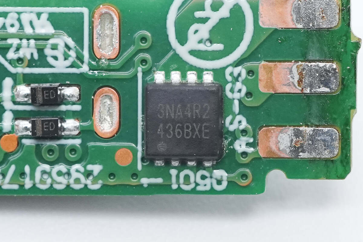
The output VBUS MOSFET is from APEC and adopts the PMPAK3*3 package. 30V 4.2mΩ. Model is AP3NA4R2YT.
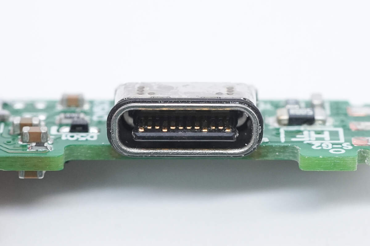
The USB-C socket is reinforced with steel sleeve.
Well, those are all components of the Original 60W PD Charger of Nintendo Switch 2.
Summary of ChargerLAB
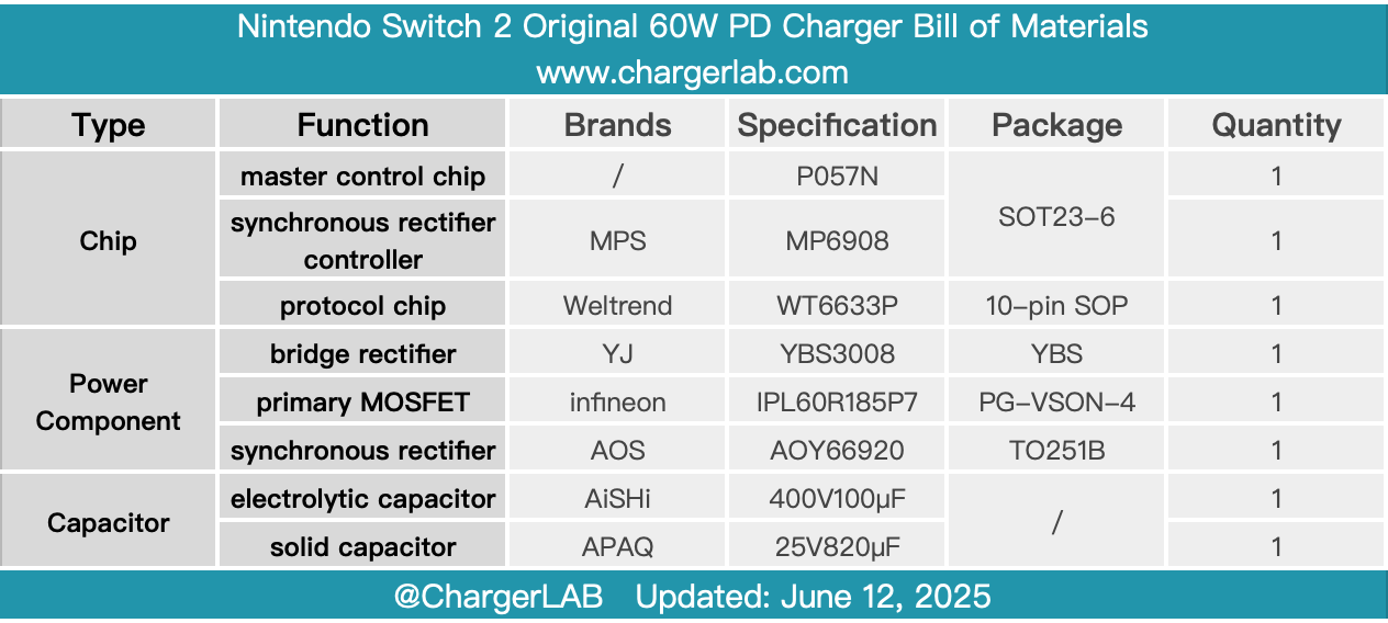
Here is the component list of the Original 60W PD Charger of Nintendo Switch 2 for your convenience.
The Nintendo Switch 2’s 60W charger features a more stylish appearance and a detachable cable design, making it more portable and convenient. Equipped with a USB-C port, it supports PD 3.0 and can deliver a maximum output of 60W, allowing it to power not only the Switch 2 but also phones, tablets, and even lightweight laptops.
After taking it apart, we found that it is based on the classic QR flyback power architecture and uses a custom master control chip paired with an MPS MP6908 synchronous rectifier controller. It also integrates an Infineon IPL60R185P7 primary MOSFET and an AOS AOY66920 synchronous rectifier, while the Weltrend WT6633P protocol chip manages the output. Additionally, it uses high-quality filter capacitors from renowned brands AiSHi and APAQ. The main components are sourced from well-known manufacturers and are assembled by Delta Electronics. The PCBA module is filled with potting compound and equipped with copper heat sinks for cooling, ensuring excellent material quality and craftsmanship.
Related Articles:
1. Unboxing of Nintendo Switch 2
2. Charging Compatibility Test of Nintendo Switch 2 (Handheld Mode)
3. How Fast Is Nintendo Switch Charged? - ChargerLAB Compatibility 100