Introduction
MOVESPEED has launched a 165W GaN desktop charger featuring 3 USB-C ports and 1 USB-A port. USB-C1 supports PD3.1 with up to 140W output, while USB-C2 and USB-C3 support 100W and 45W PD output, respectively. The USB-A port provides 30W output and is compatible with fast charging protocols such as UFCS, QC, SCP, FCP, and AFC. With a thickness of just 2cm, this desktop charger offers a sleek design. Next, we will take a closer look at its internal design and components.
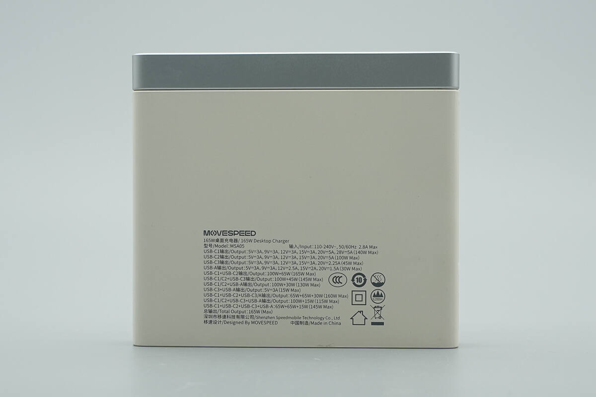
Product Appearance
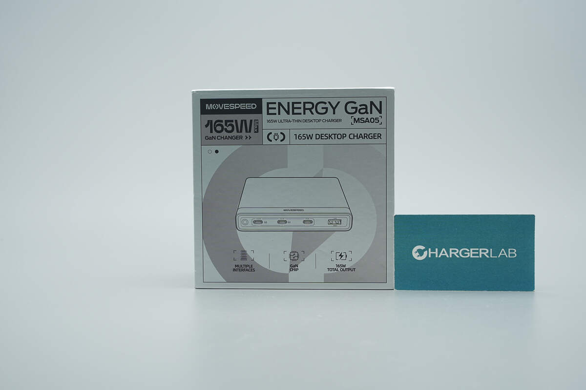
The front of the packaging features the MOVESPEED logo, an illustration of the product's appearance, and key selling points.
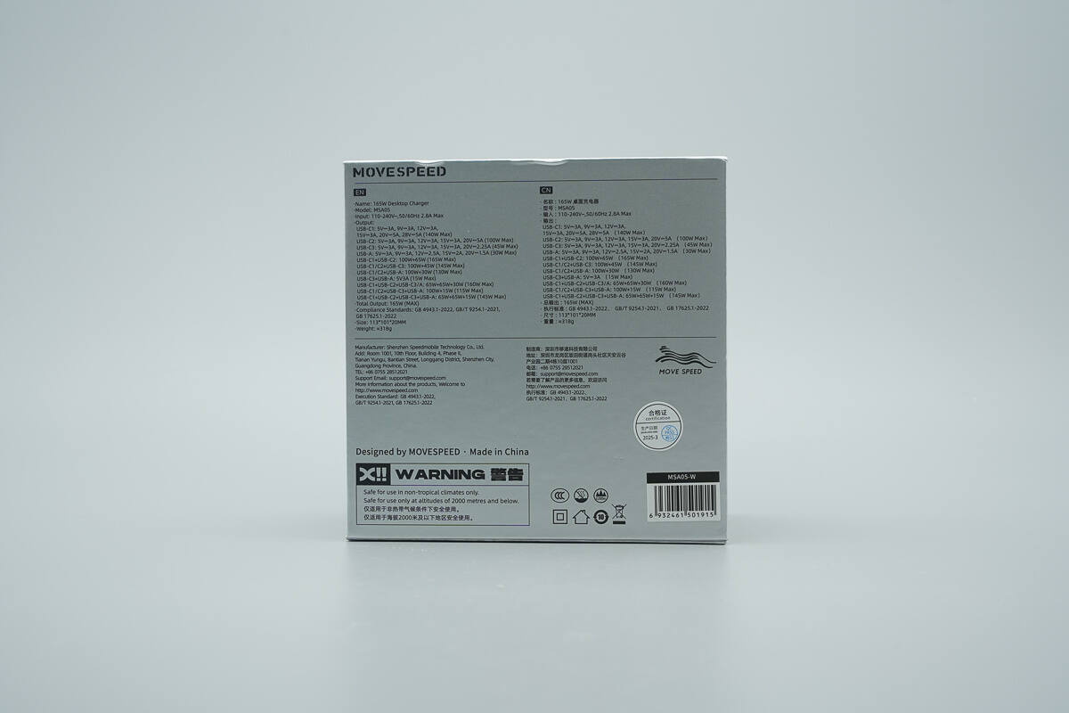
The back of the packaging displays the product specifications, vendor information, and important notices.
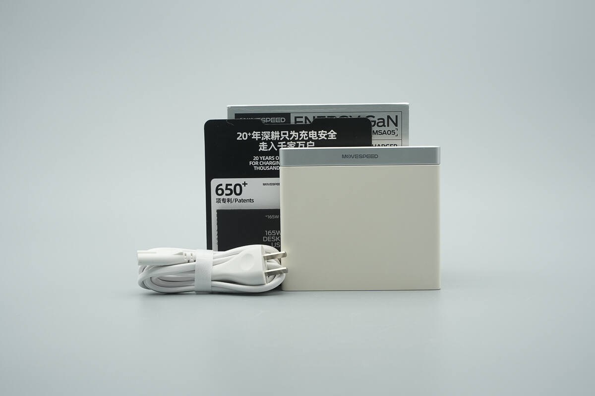
The package includes the desktop charger, a power cable, and a user manual.
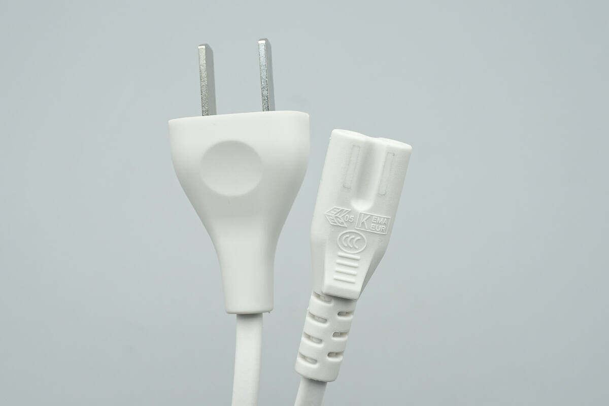
The power cable features a two-prong plug on one end and a figure-eight plug on the other.
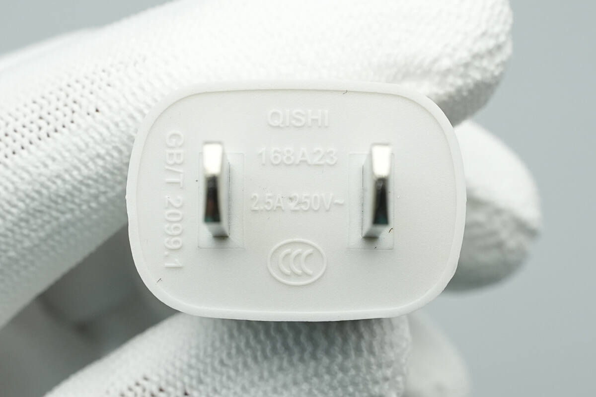
The power cable is rated at 2.5A 250V~ and has passed CCC certification.
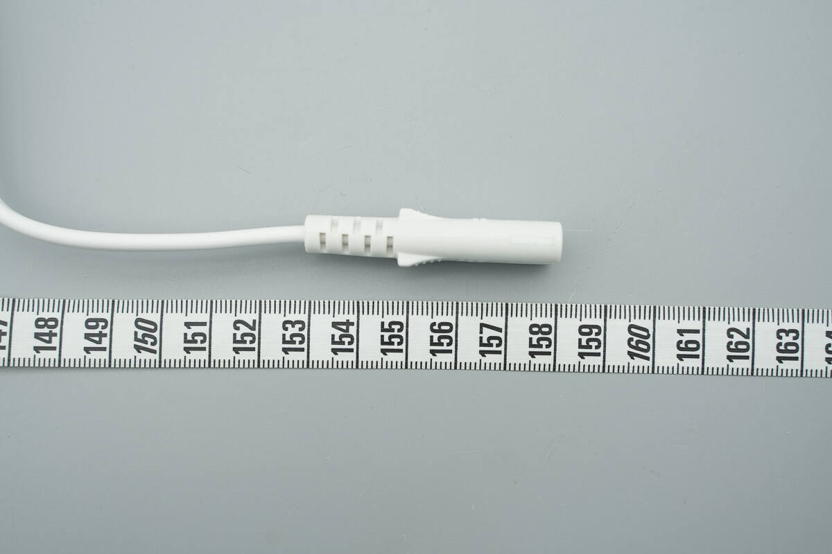
The length is about 158 cm (62.2 inches).
The exterior is made of flame-retardant material with a matte finish.
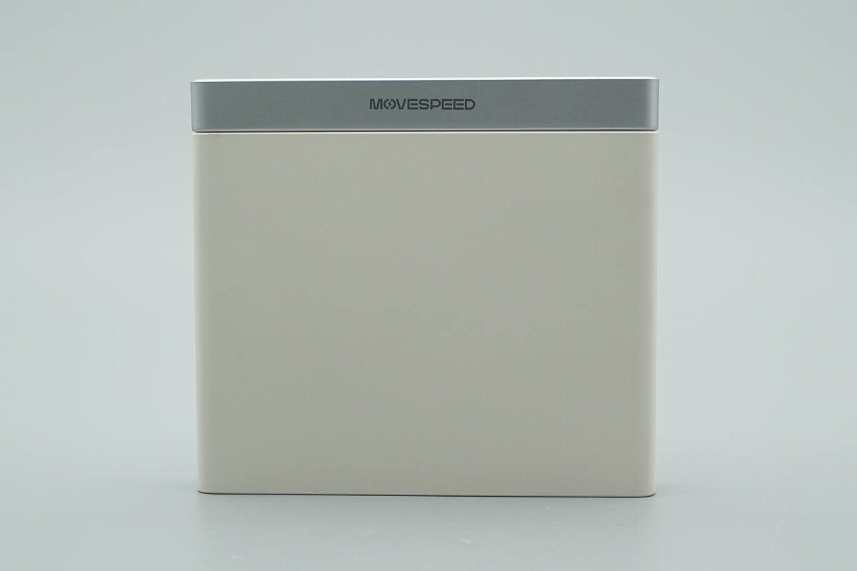
The front is coated with silver-gray metallic paint and features the MOVESPEED logo.
The bottom of the casing has the product's specification information printed on it.
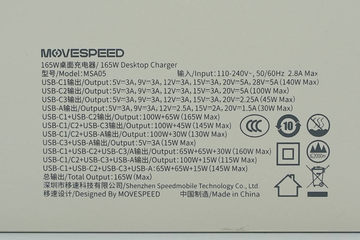
Model: MSA05
Input: 110-240V~, 50/60Hz 2.8A Max
Output:
USB-C1: 5V3A, 9V3A, 12V3A, 15V3A, 20V5A, 28V5A (140W Max)
USB-C2: 5V3A, 9V3A, 12V3A, 15V3A, 20V5A (100W Max)
USB-C3: 5V3A, 9V3A, 12V3A, 15V3A, 20V2.25A (45W Max)
USB-A: 5V3A, 9V3A, 12V2.5A, 15V2A, 20V1.5A (30W Max)
USB-C1 + USB-C2: 100W + 65W (165W Max)
USB-C1/C2 + USB-C3: 100W + 45W (145W Max)
USB-C1/C2 + USB-A: 100W + 30W (130W Max)
USB-C3 + USB-A: 5V3A (15W Max)
USB-C1 + USB-C2 + USB-C3/A: 65W + 65W + 30W (160W Max)
USB-C1/C2 + USB-C3 + USB-A: 100W + 15W (115W Max)
USB-C1 + USB-C2 + USB-C3 + USB-A: 65W + 65W + 15W (145W Max)
Total Output: 165W (Max)
The product is CCC certified.
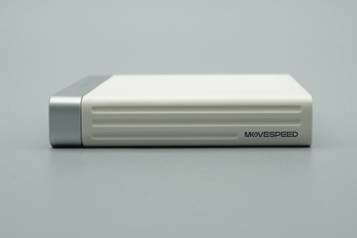
One side is printed with the MOVESPEED logo.
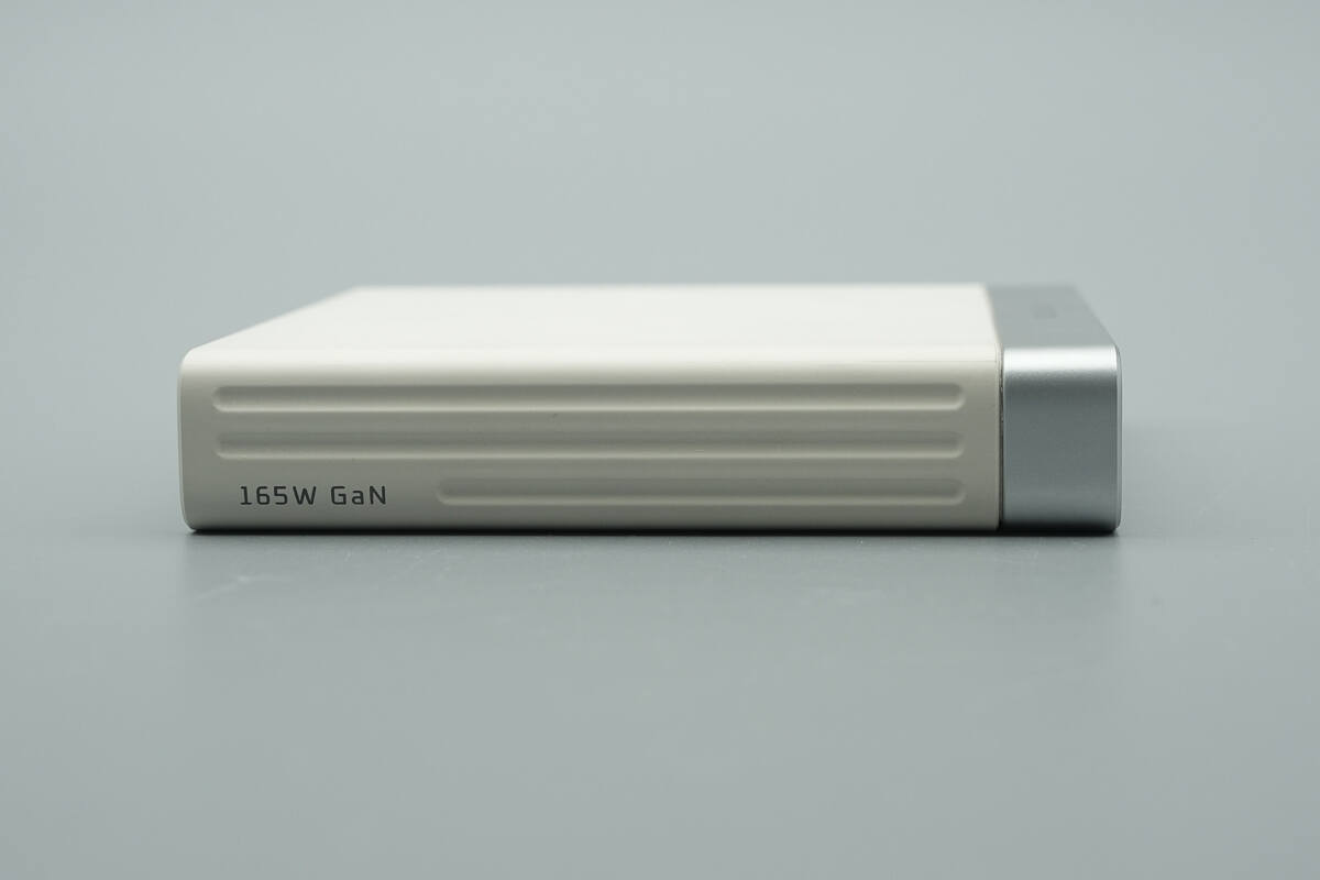
The other side is printed with "165W GaN."
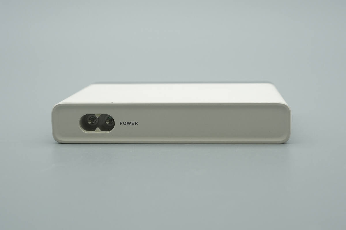
The back features the power input port.
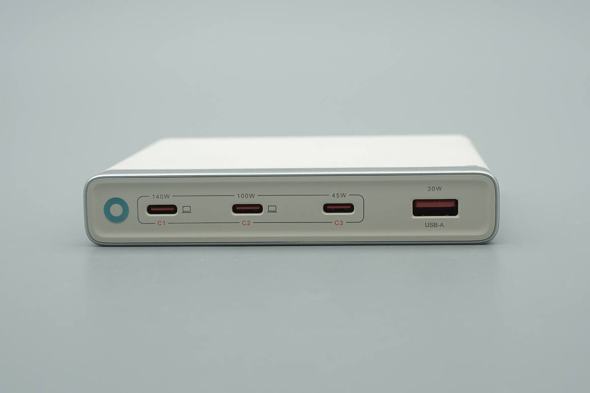
It is equipped with 3 USB-C ports and 1 USB-A port, with the corresponding output power printed next to each port.
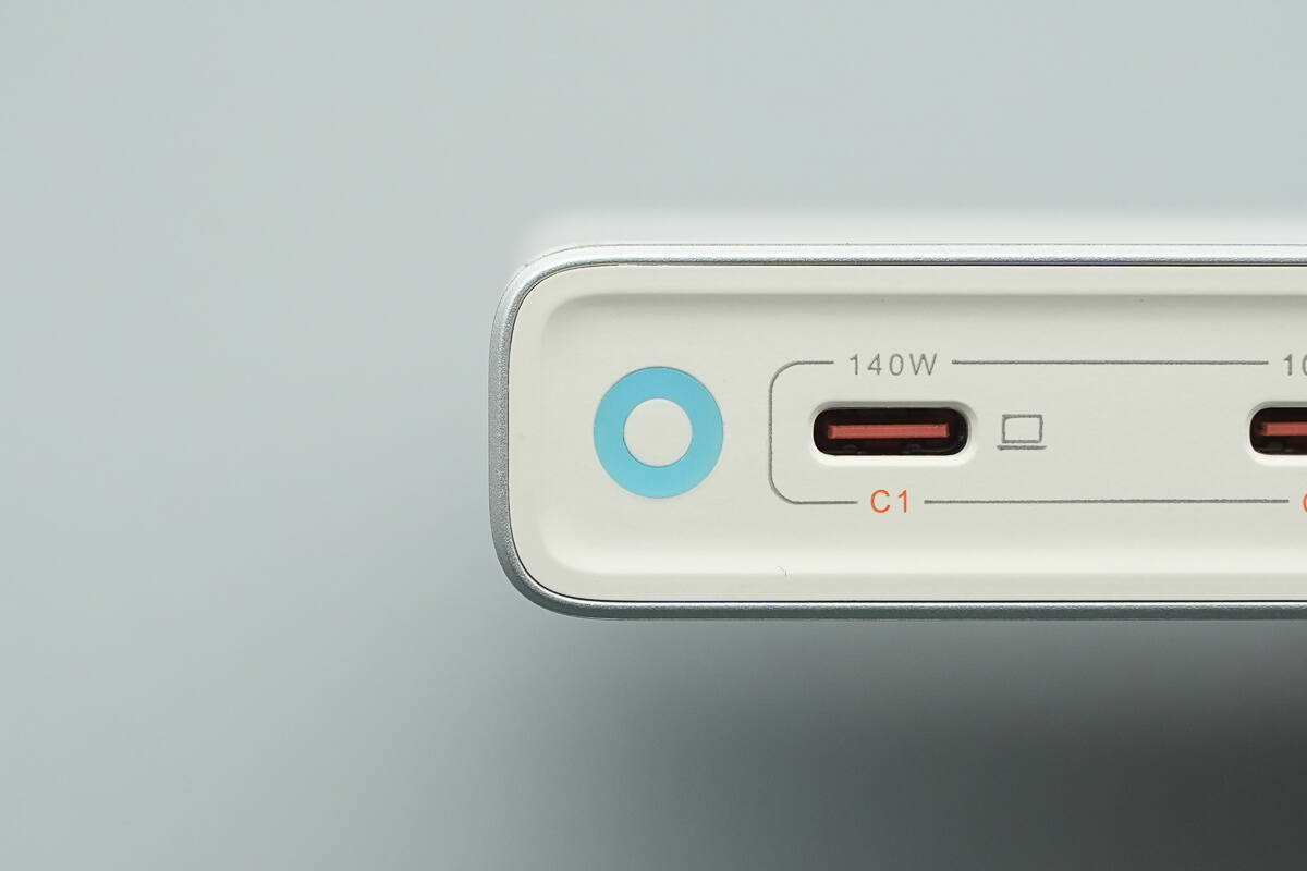
The left side features an indicator light ring.
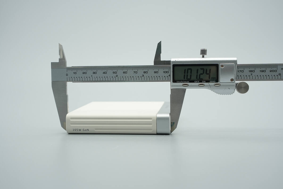
The length of the charger is about 101.24 mm (3.99 inches).
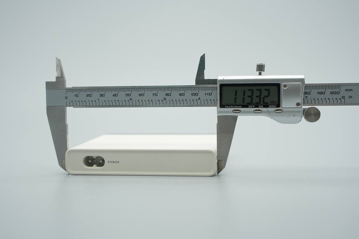
The width is about 113.32 mm (4.46 inches).
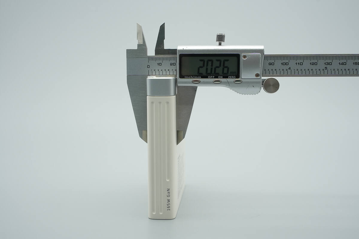
The thickness is about 20.26 mm (0.8 inches).
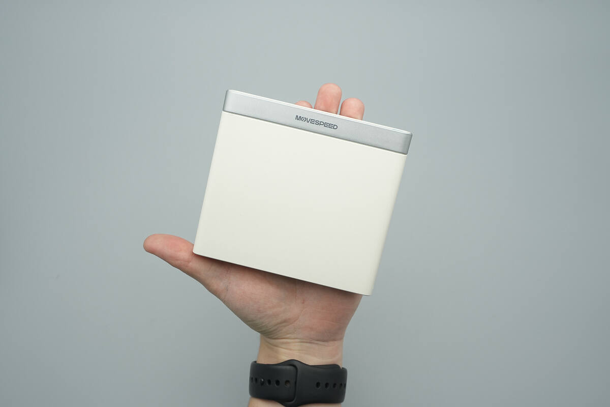
That's how big it is on the hand.
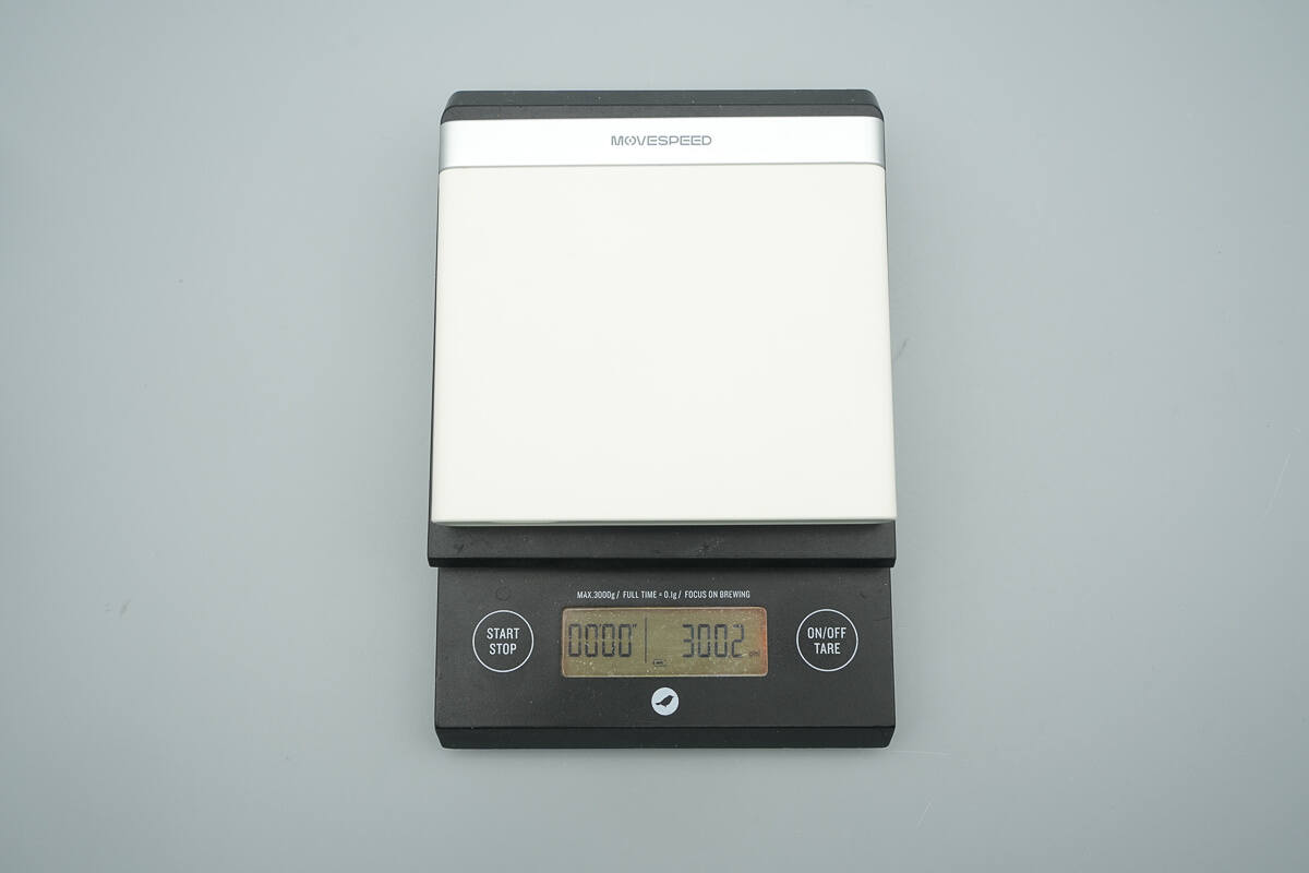
The weight is about 300 g (10.58 oz).
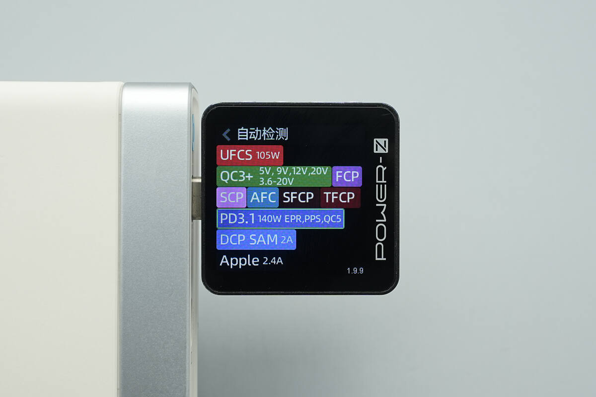
ChargerLAB POWER-Z KM003C shows that the USB-C1 port supports UFCS, QC3+/5, FCP, SCP, AFC, SFCP, TFCP, PD3.1, PPS, DCP, SAM 2A, and Apple 2.4A charging protocols.
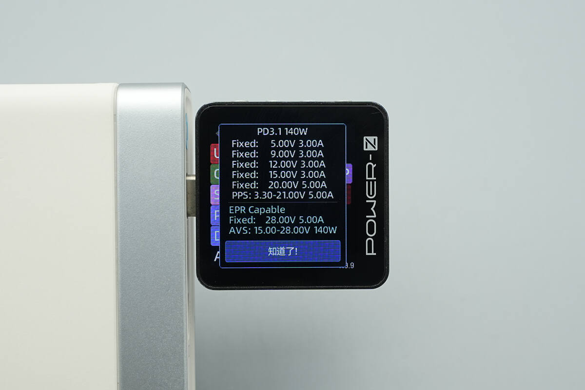
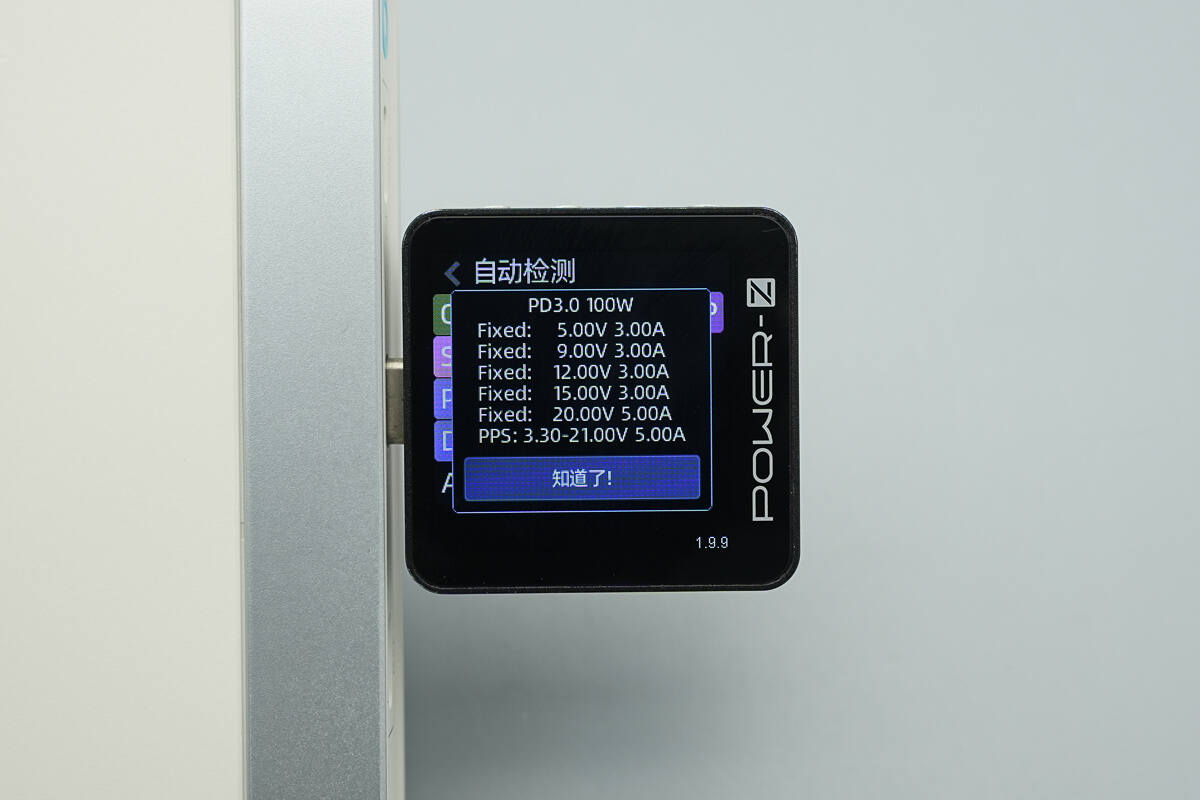
It features six fixed PDOs of 5V3A, 9V3A, 12V3A, 15V3A, 20V5A, and 28V5A, as well as 3.3-21V5A PPS voltage levels and 15-28V 140W AVS voltage levels.
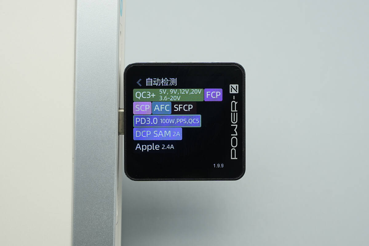
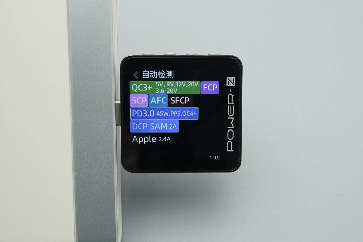
The USB-C2 port supports QC3+/5, FCP, SCP, AFC, SFCP, PD3.0, PPS, DCP, SAM 2A, and Apple 2.4A charging protocols.
It features five fixed PDOs of 5V3A, 9V3A, 12V3A, 15V3A, 20V5A, along with a 3.3-21V5A PPS voltage range.
The USB-C3 port supports QC3+/4+, FCP, SCP, AFC, SFCP, PD3.0, PPS, DCP, SAM 2A, and Apple 2.4A charging protocols.
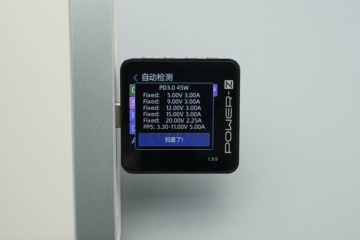
It features five fixed PDOs of 5V3A, 9V3A, 12V3A, 15V3A, 20V2.25A, along with a 3.3-11V5A PPS voltage range.
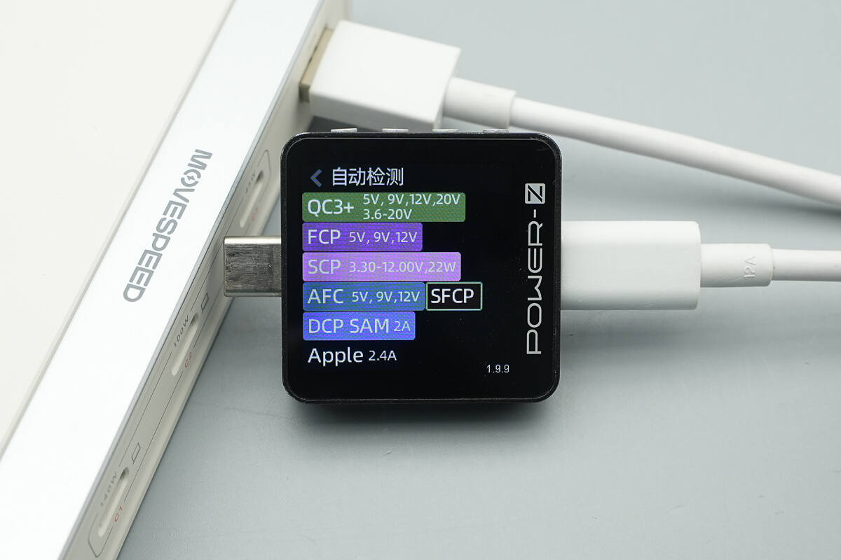
The USB-A port supports QC3+, FCP, SCP, AFC, SFCP, DCP, SAM 2A, and Apple 2.4A charging protocols.
Teardown
Next, let's take it apart to see its internal components and structure.
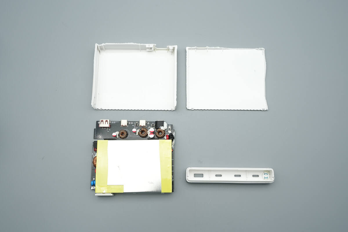
Cut the outer shell to remove the PCBA module.
Both the front and back of the module are covered with heat sinks, which are secured in place using clips.
The inner side of the bottom heat sink is equipped with a Mylar sheet for isolation and insulation.
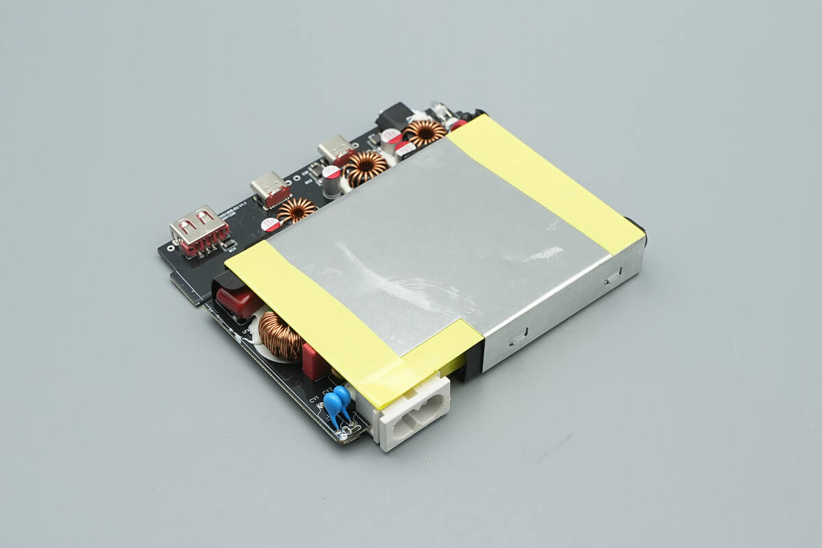
The small PCB at the output end and the PCBA module are connected through red and black wires soldered together.
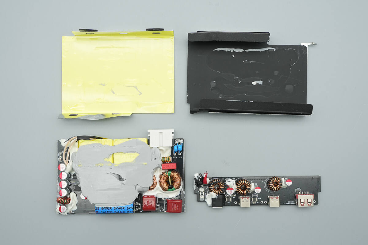
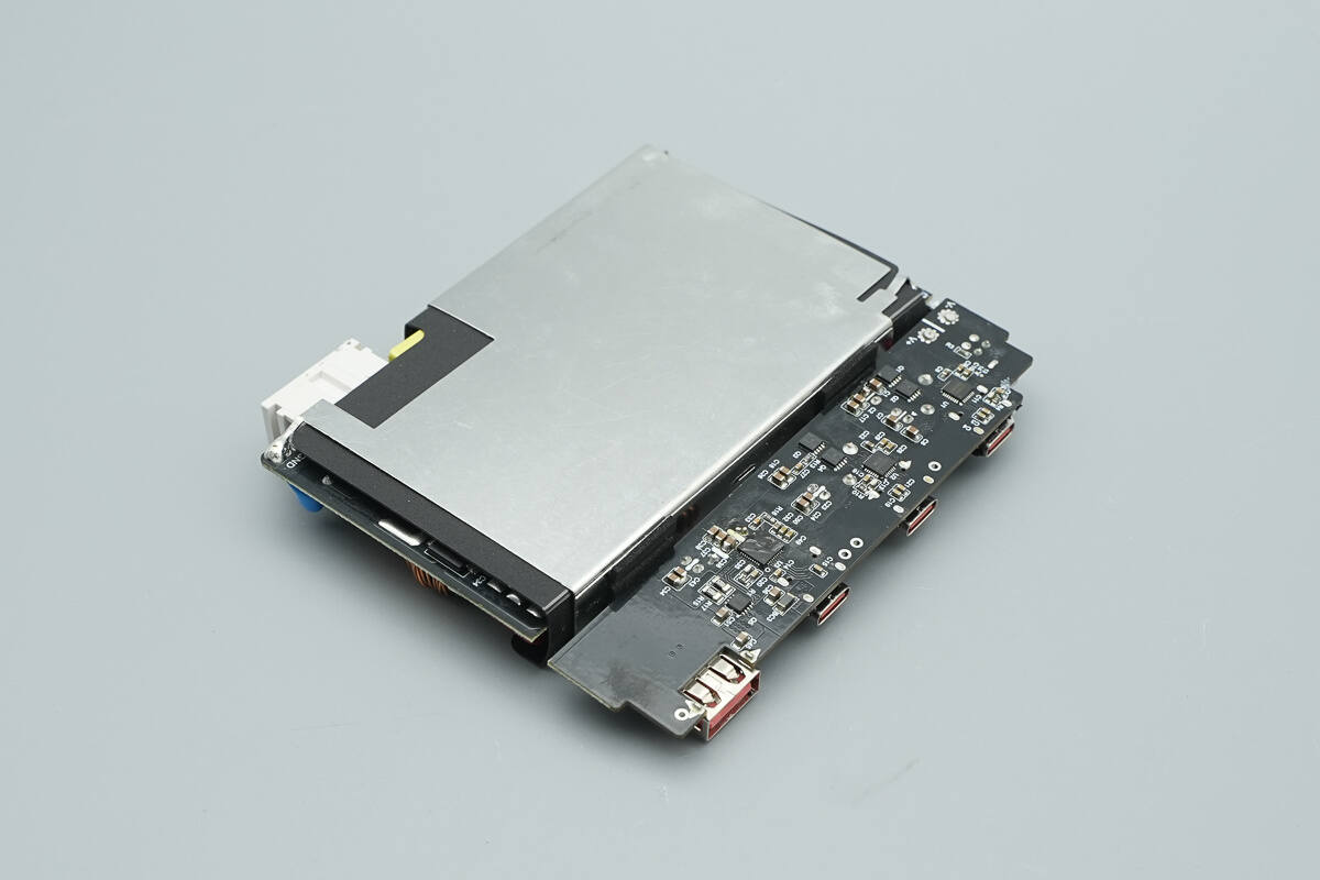
Remove the heat sinks to separate the two PCBs.
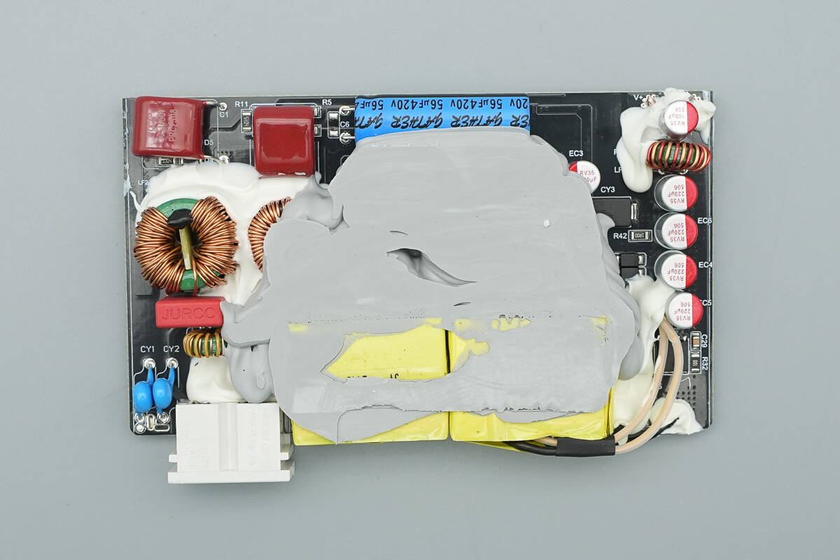
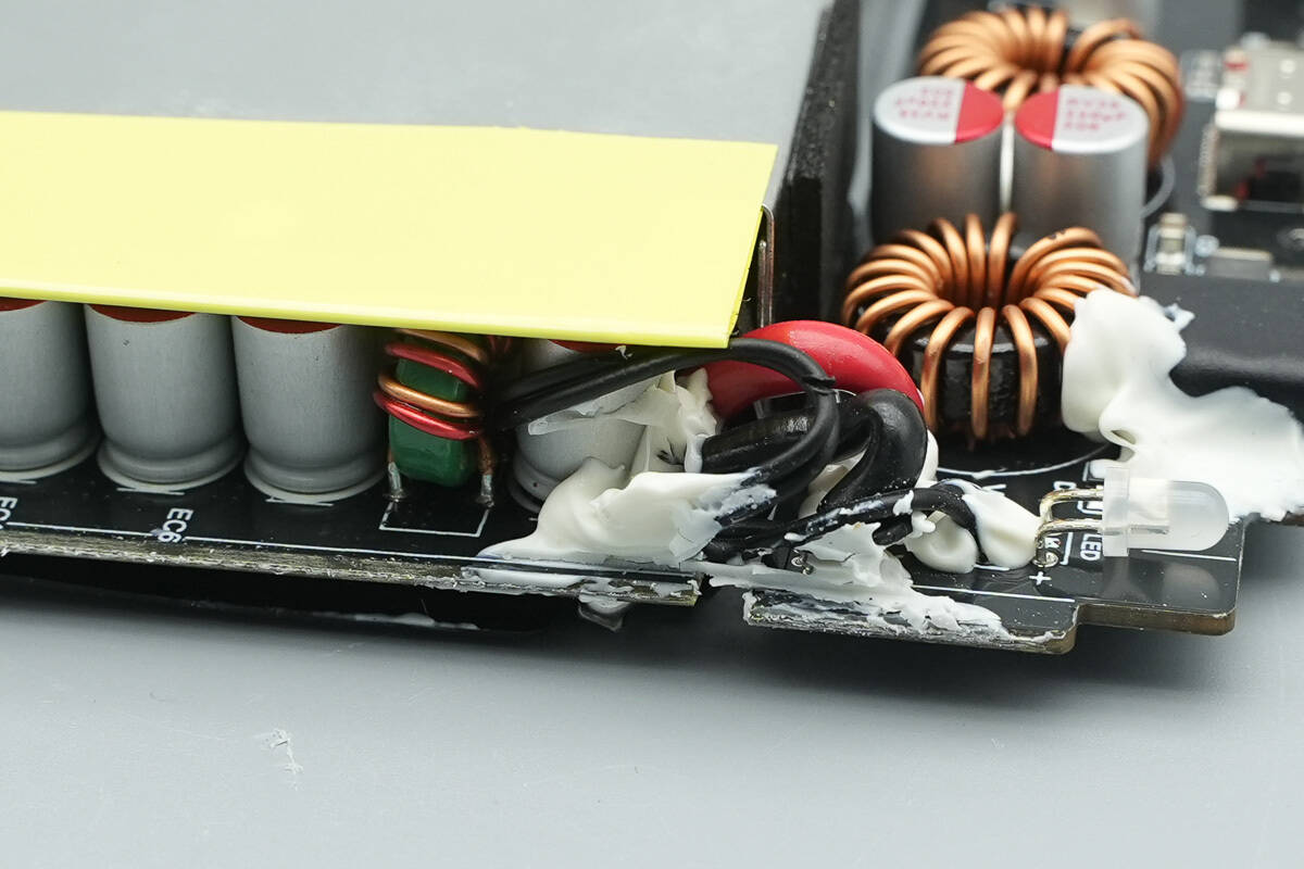
The PCBA module is heavily filled with thermal adhesive to assist with heat dissipation.
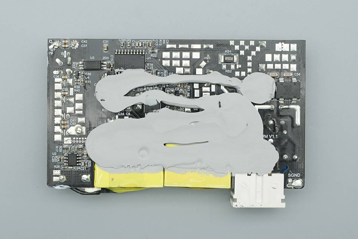
The backside is also coated with adhesive to aid in heat dissipation.
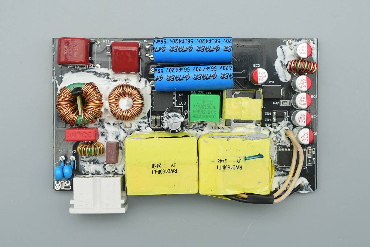
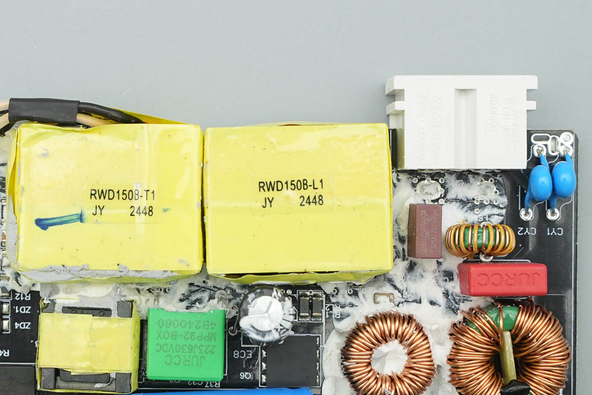
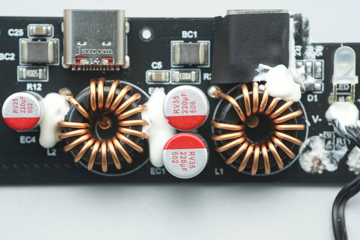
Remove the adhesive. The front of the PCBA module contains components such as a fuse, common mode chokes, film capacitors, filter inductors, PFC boost inductors, electrolytic capacitors, resonant capacitors, transformers, and solid capacitors.
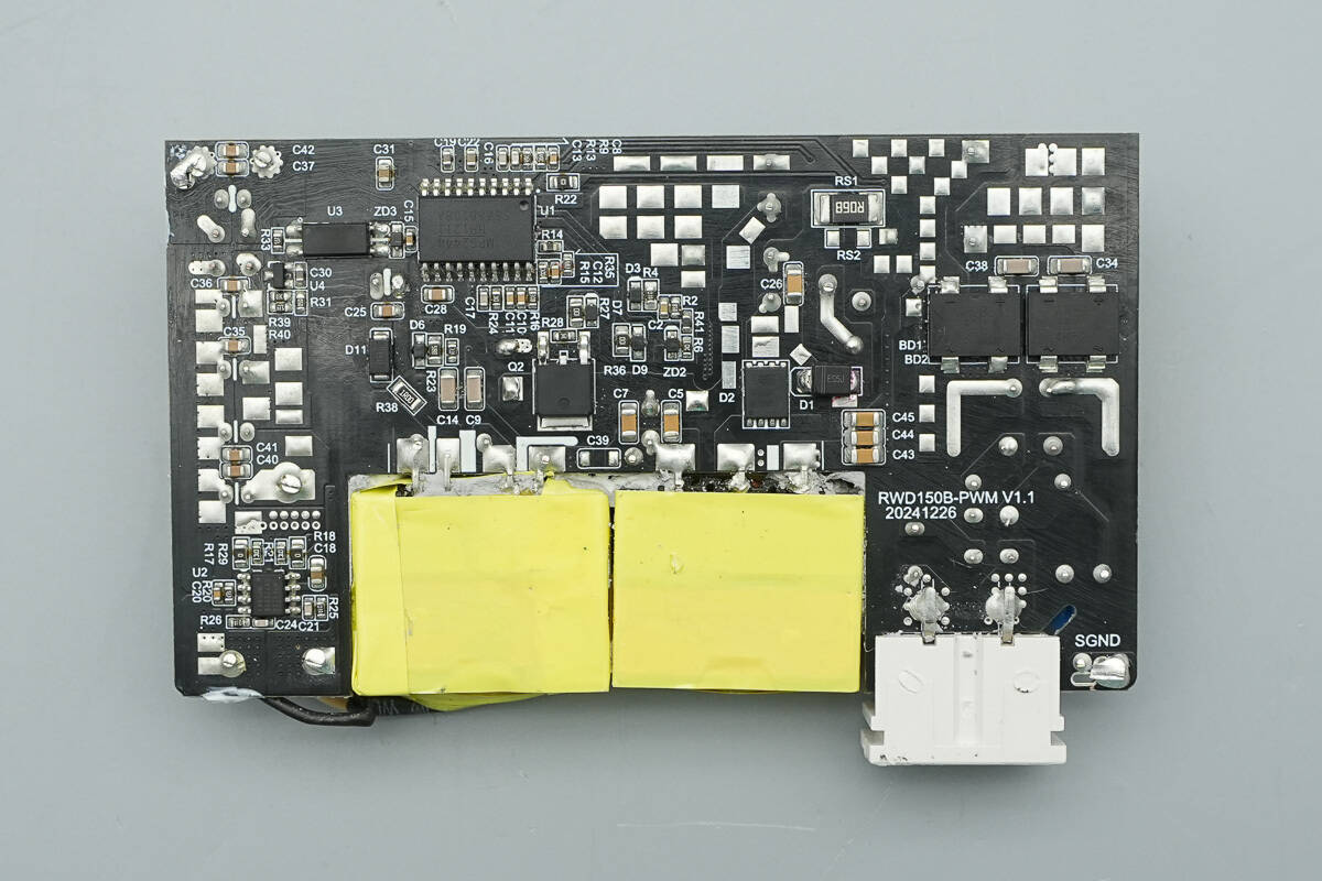
The backside of the PCBA module features bridge rectifiers, the master control chip, PFC rectifiers, LLC MOSFETs, an optocoupler, and a synchronous rectifier controller.
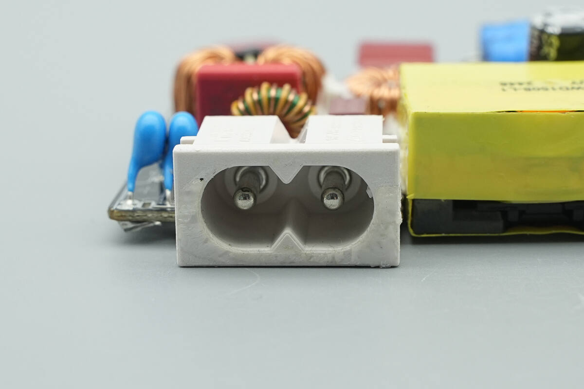
A close-up of the input socket.
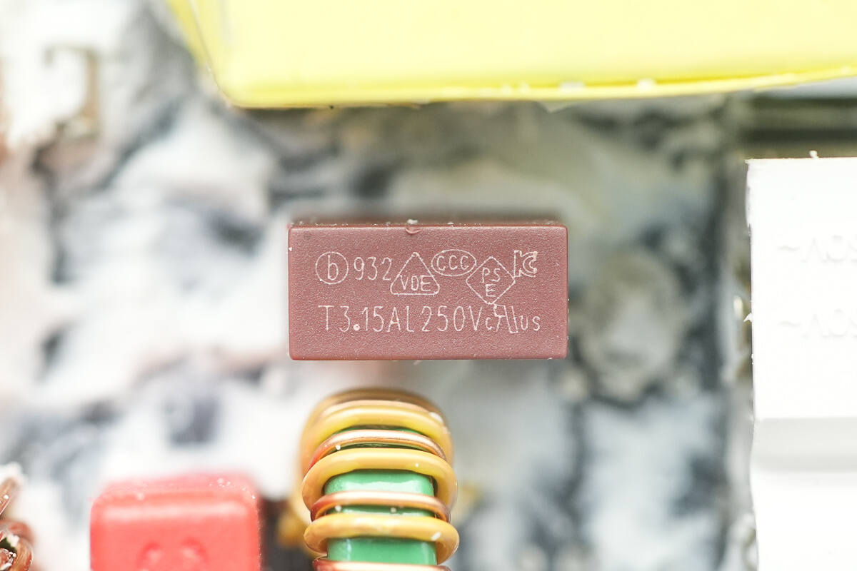
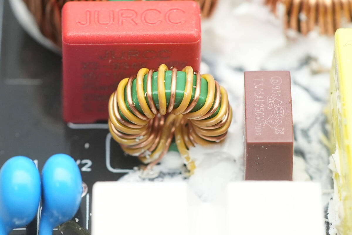
The time-delay fuse is from Betterfuse, with part number 932 and a rating of 3.15A 250V.
The common mode choke is wound with two wires and is used to filter out EMI.
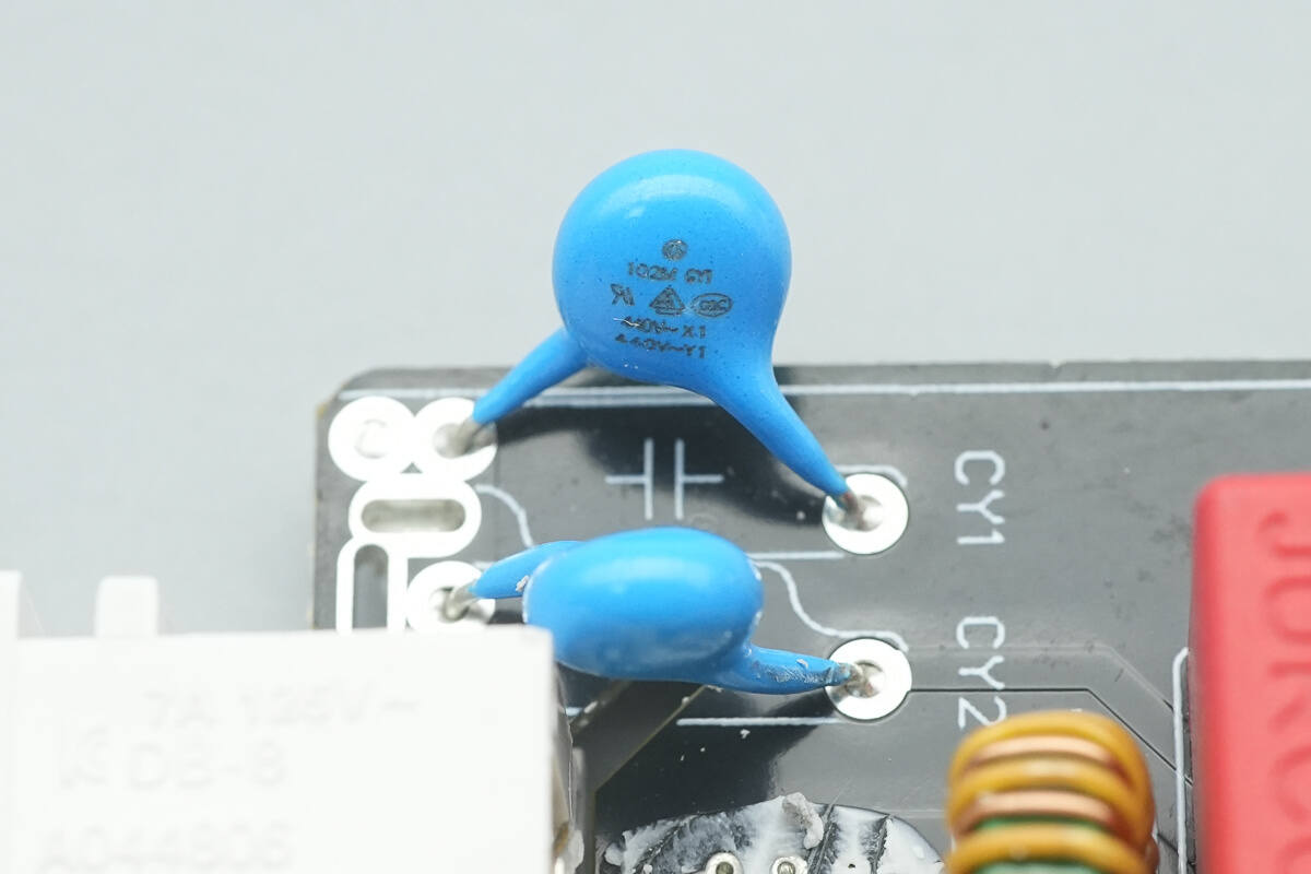
A close-up of the two blue capacitors.
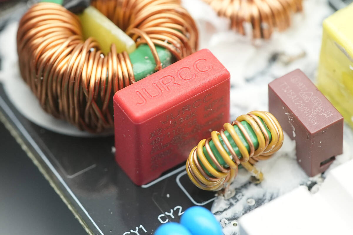
The safety X2 capacitor is from JURCC, with a specification of 0.33μF.
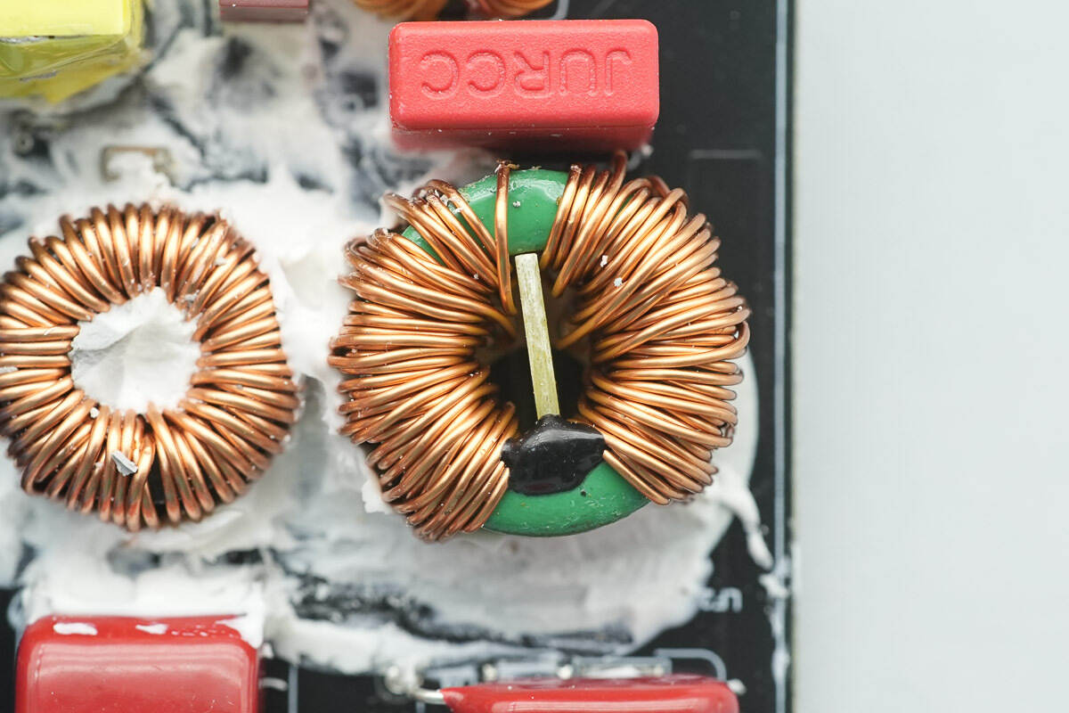
A close-up of the other common mode choke.
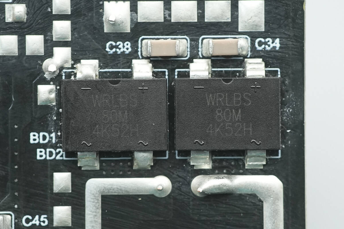
The input bridge rectifiers are from World Industrial, model WRLBS80M, with a specification of 8A 1000V. These soft bridge rectifiers, with their softer recovery curves and smoother turn-off characteristics, help reduce diode junction capacitance and minimize the generation of harmonic oscillations. They come in an LBS package.
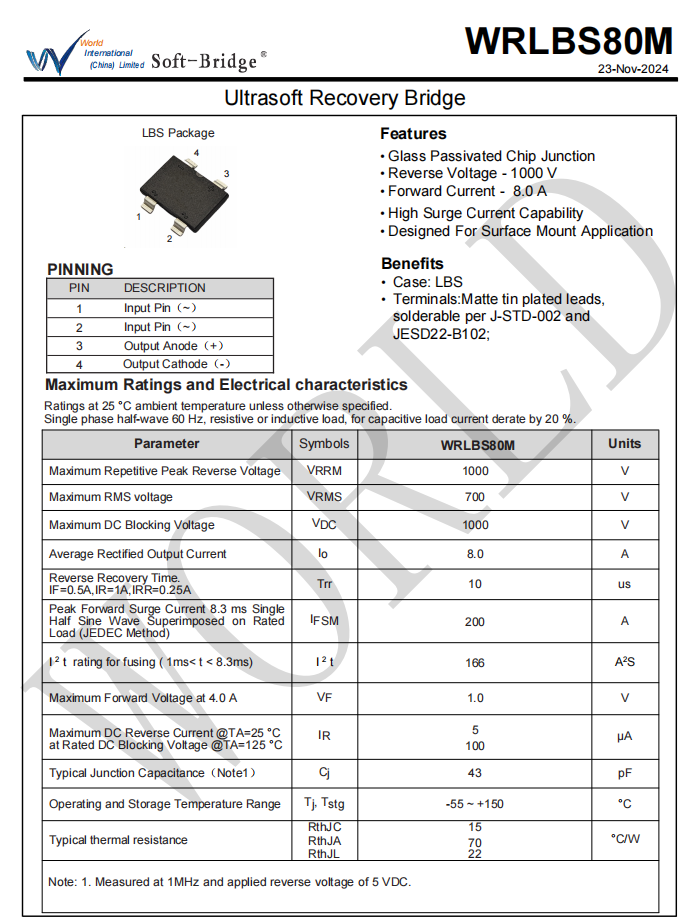
Here is the information about World Industrial WRLBS80M.
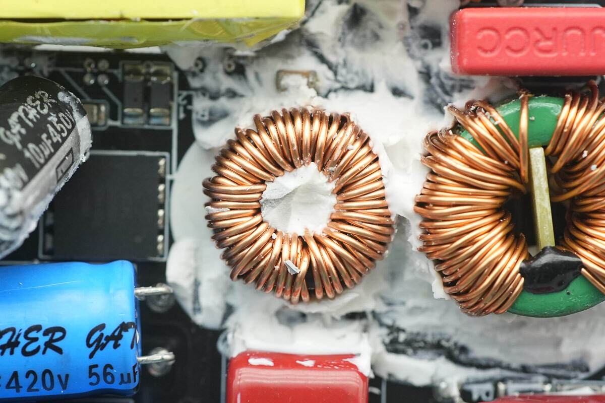
A close-up of the filter inductor.
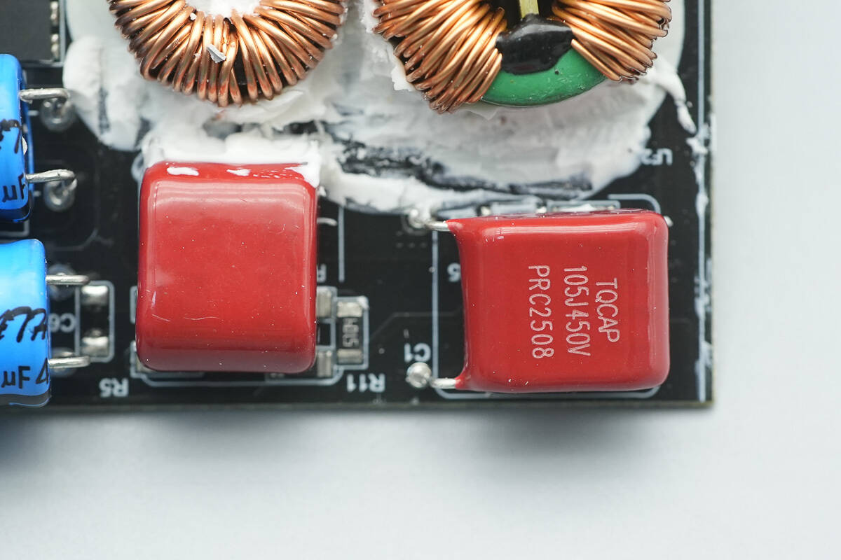
The two film capacitors are from TQCAP, both with a specification of 1μF 450V.
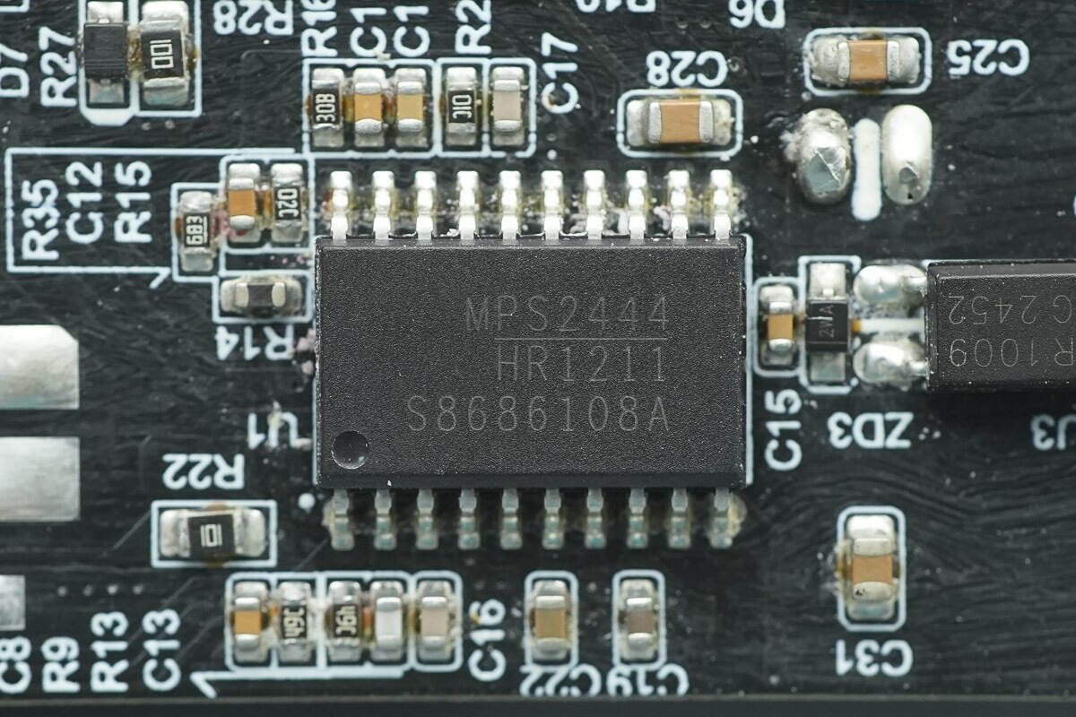
The master control chip is from MPS, model HR1211. It is a multi-mode PFC and current-mode LLC combined controller, integrating the functions that traditionally required 2-3 chips into a single chip. The PFC controller supports both CCM and DCM operating modes.
The HR1211 uses a digital control core, supports high-voltage startup, and features intelligent X-capacitor discharge. The PFC stage supports a maximum operating frequency of 250KHz, while the LLC stage includes a 600V half-bridge driver with an integrated bootstrap diode. The operating frequency reaches up to 500KHz and supports a range of protection functions. It comes in an SOIC-20 package.
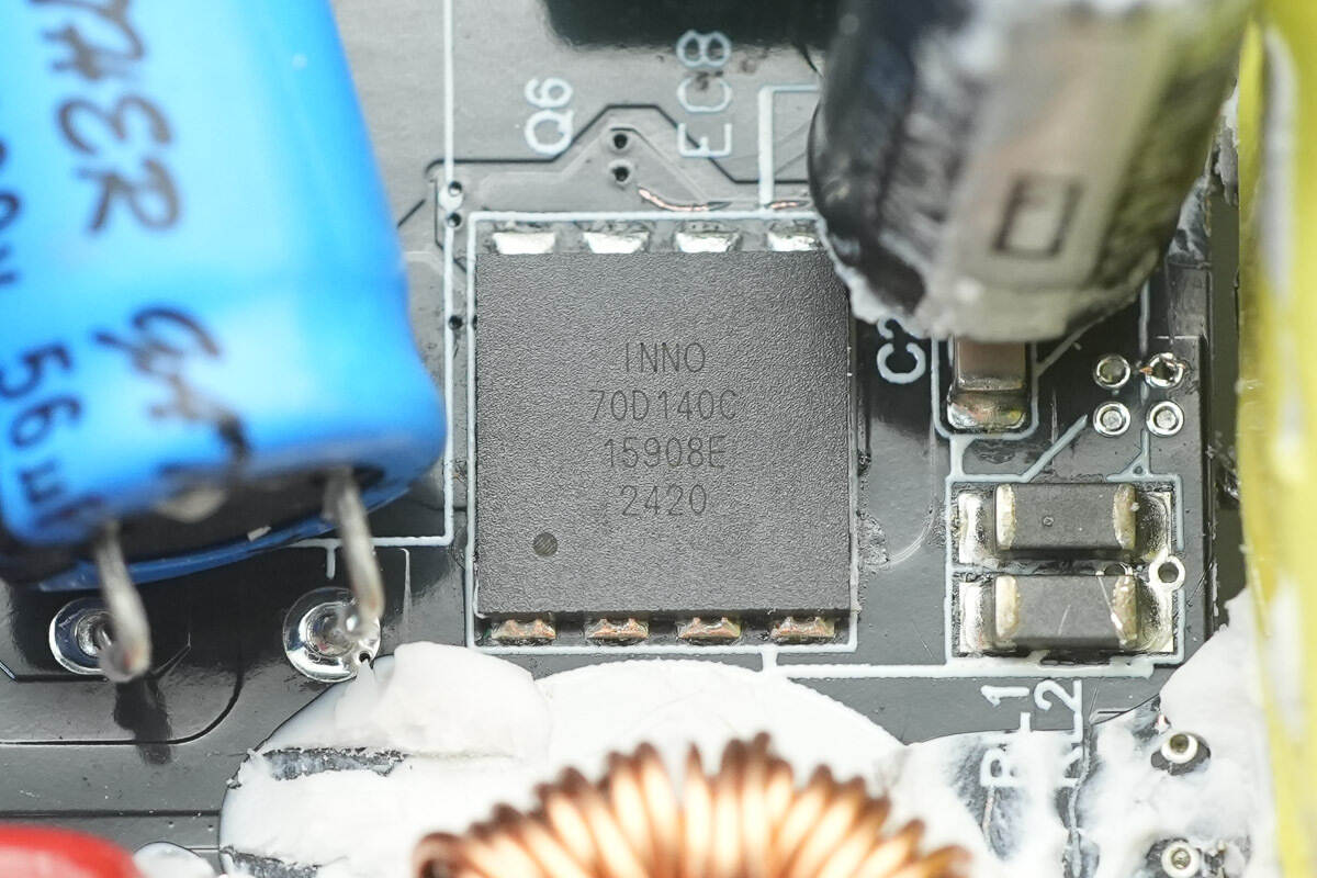
The PFC MOSFET is from Innoscience, marked with 70D140C, and model INN700D140C. It is an enhanced GaN FET with a voltage rating of 700V and a transient voltage rating of 800V. The on-resistance is 140mΩ, and it features a Kelvin source. The device is packaged in a DFN 8*8 package, with two units connected in parallel.
Innoscience's GaN FETs have extremely low gate charge and output charge, meeting the industrial application requirements of JEDEC standards. They also include built-in ESD protection and comply with RoHS, lead-free, and EU REACH regulations. These MOSFETs are suitable for totem-pole PFCs, fast-charging power supplies, high power density, and high-efficiency switch-mode power supply applications.
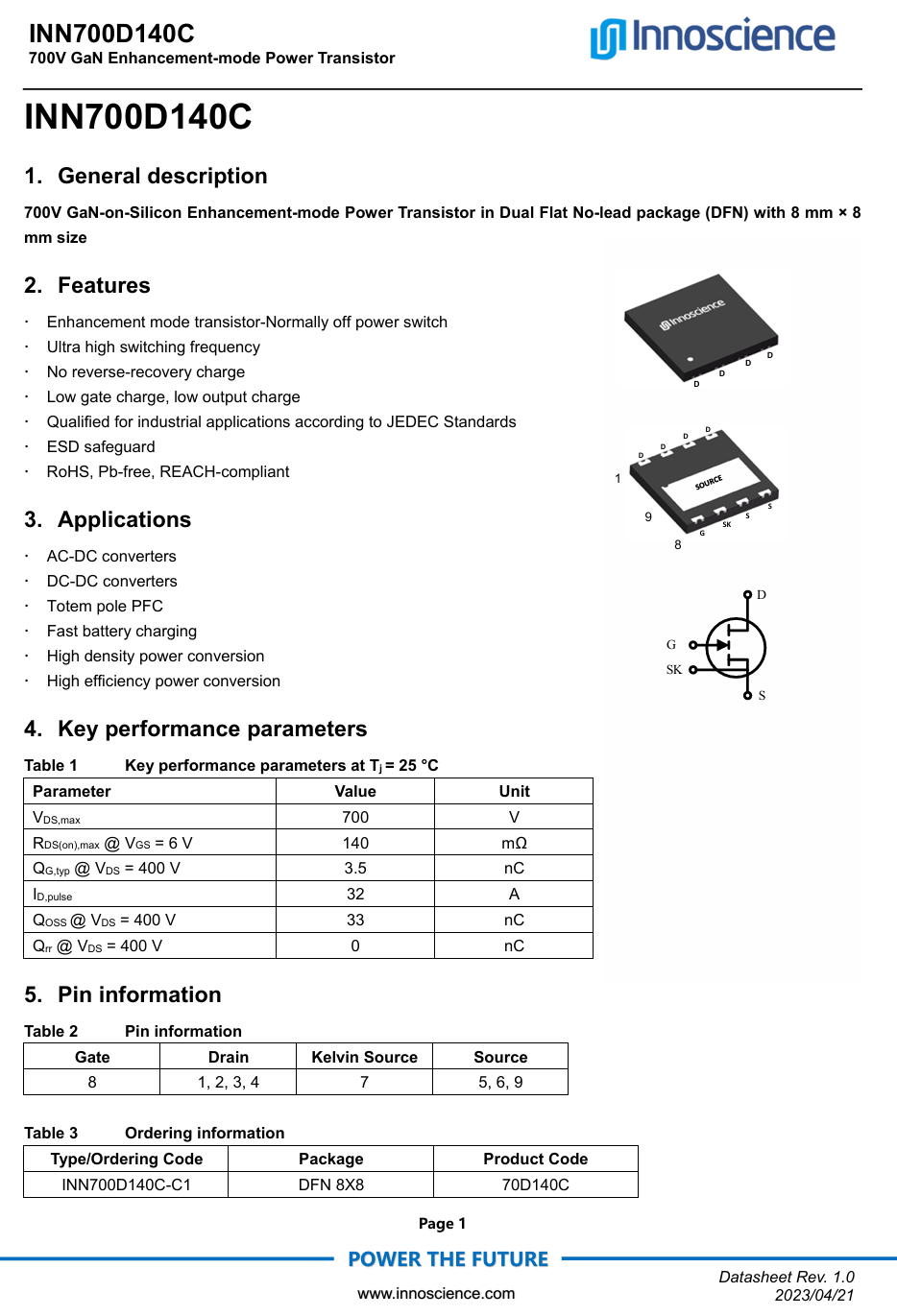
Here is the information about Innoscience INN700D140C.
A close-up of the PFC boost inductors.
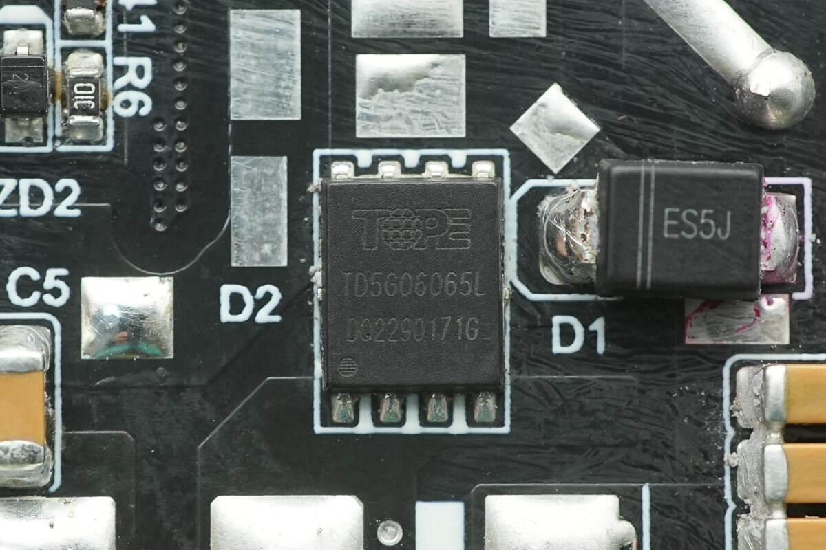
The PFC rectifier is from TOPE, model TD5G06065L. It is a silicon carbide Schottky diode with a voltage rating of 650V and comes in a DFN 5*6 package.
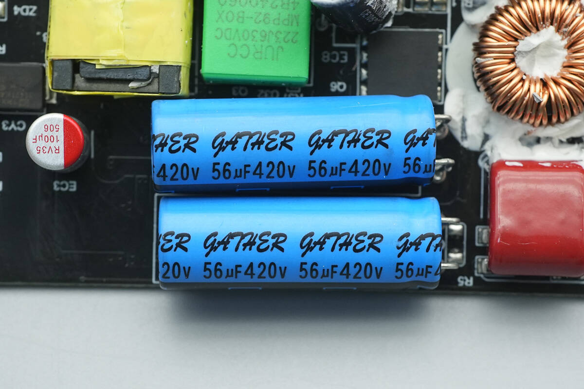
The two high-voltage filter electrolytic capacitors are from GATHER, both with a specification of 420V 56μF.

There is also one capacitor with a specification of 450V 10μF.
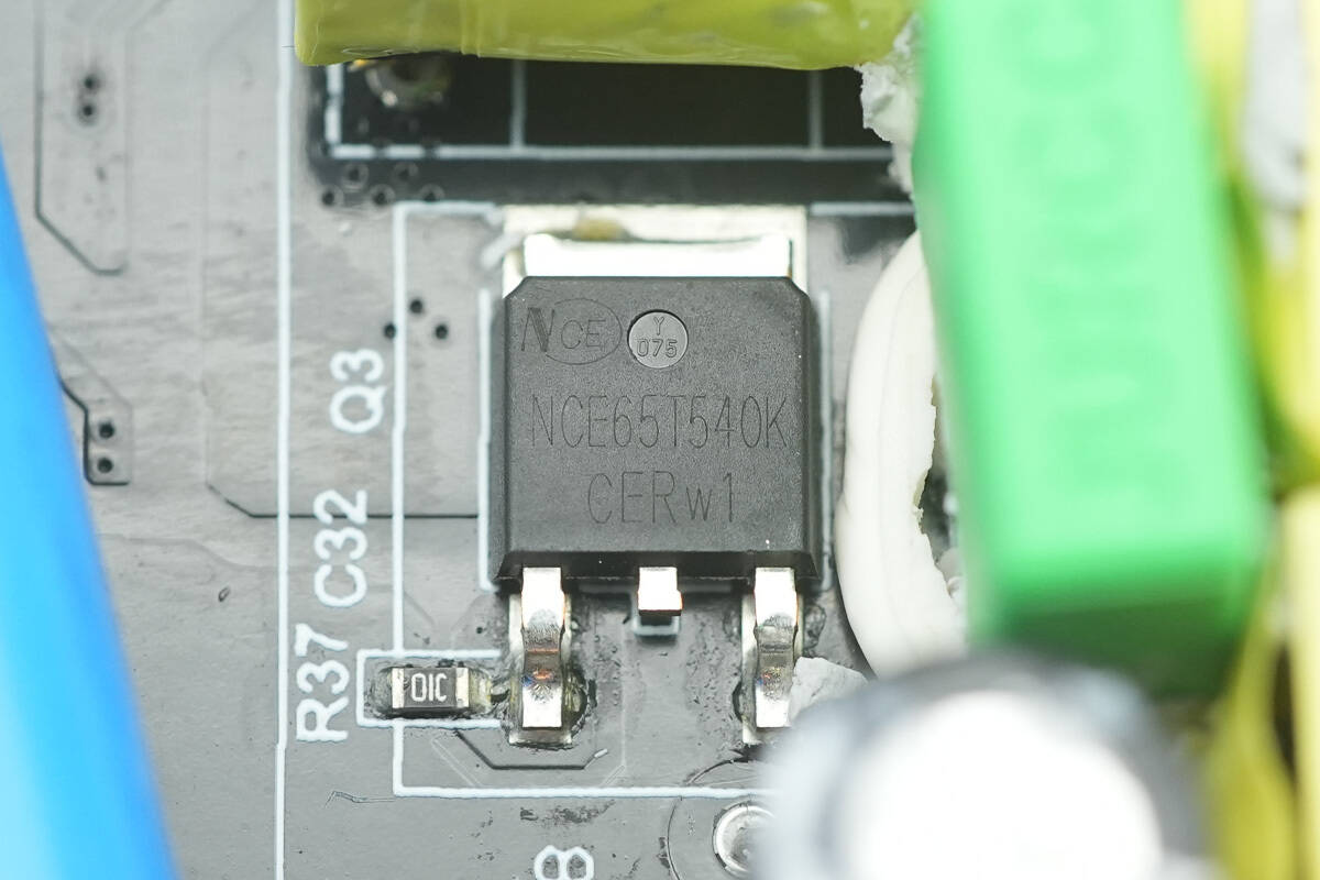
The LLC MOSFET is from NCEPower, model NCE65T540K. It is an NMOS transistor with a voltage rating of 650V and an on-resistance of 460mΩ. It comes in a TO-252 package.
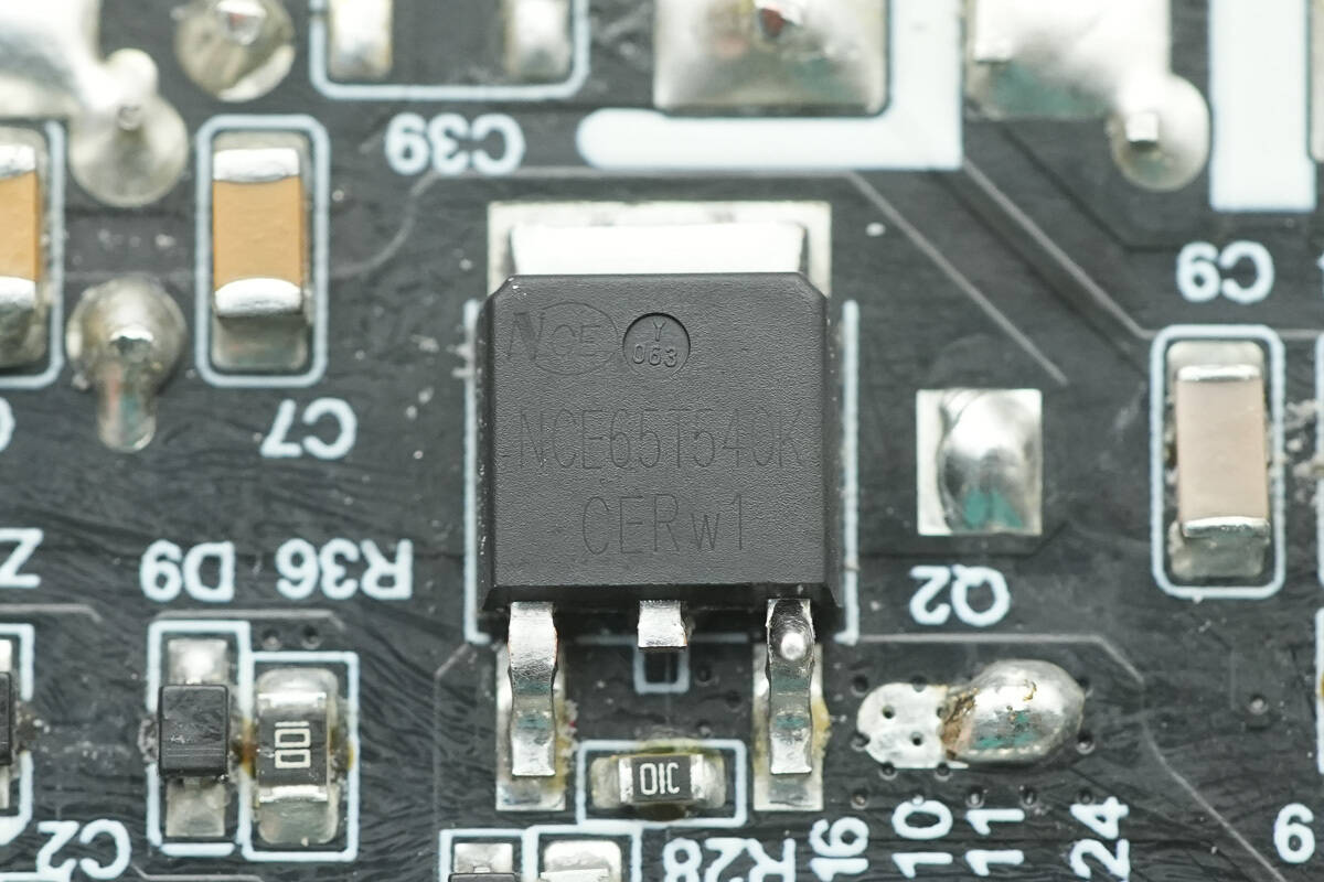
Another NCEPower NCE65T540K LLC MOSFET is located on the backside of the PCBA module.
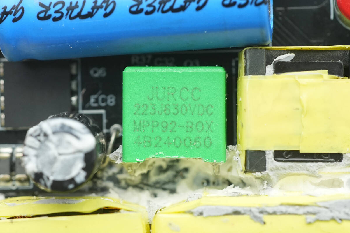
The resonant capacitor is from JURCC, with a specification of 0.022μF 630V.
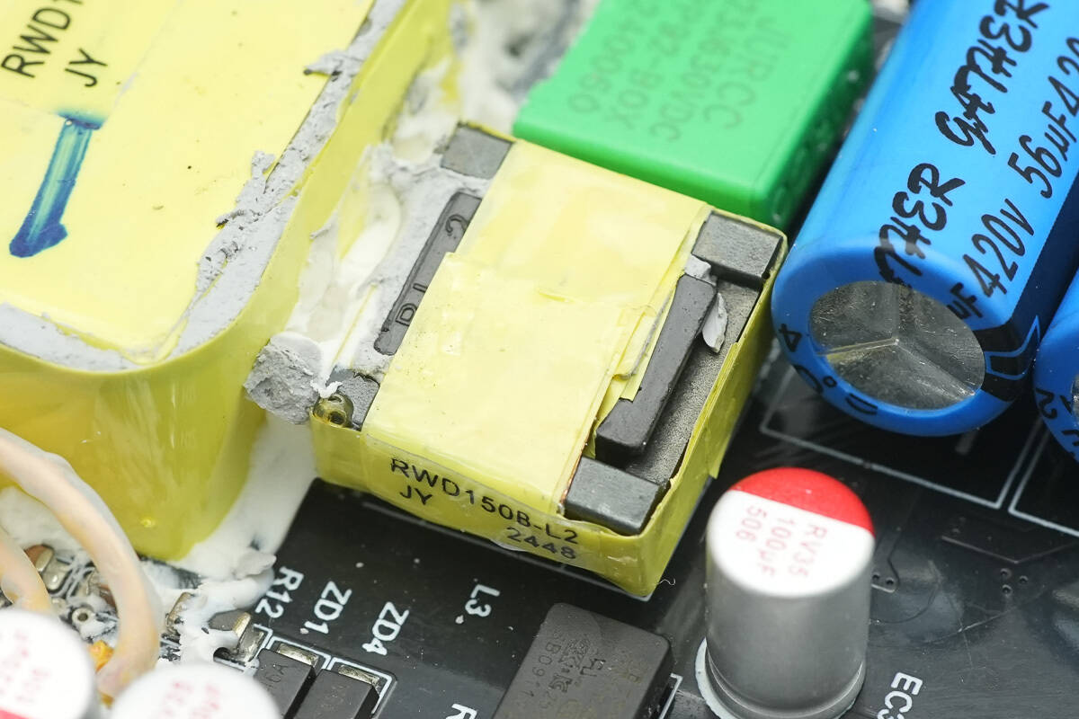
A close-up of the resonant inductor.
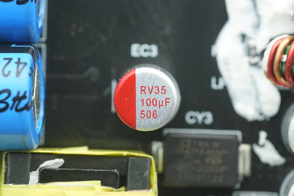
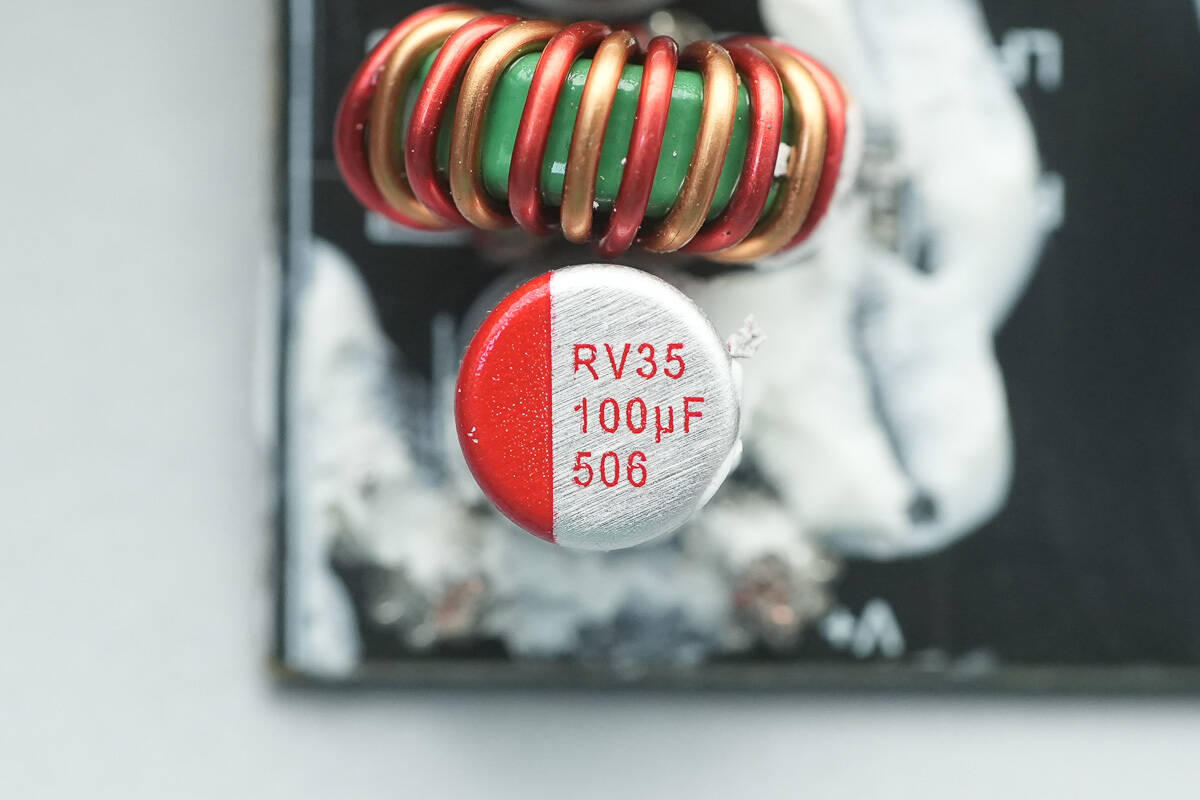
The capacitor that supplies power to the master control chip has a specification of 35V 100μF.
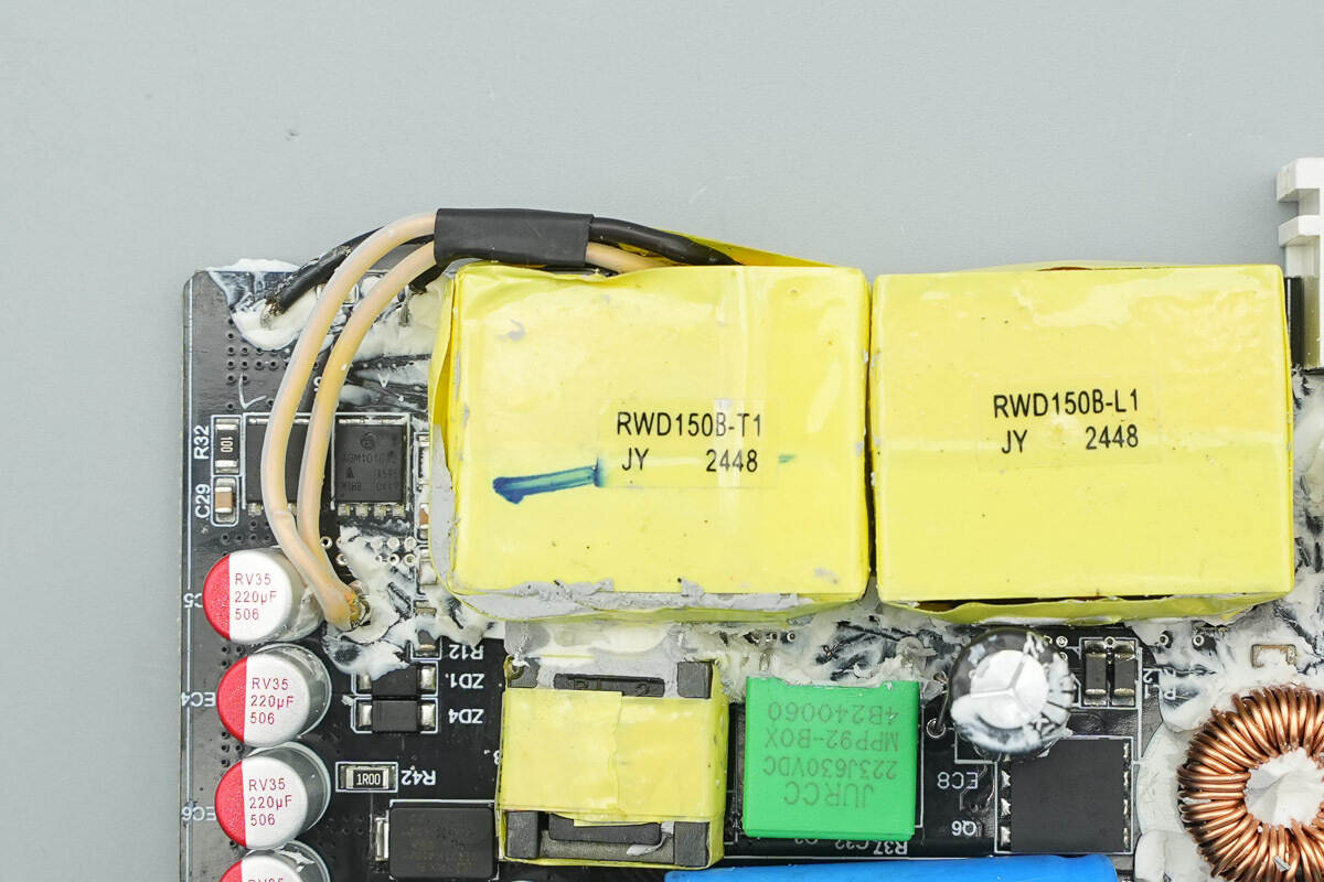
A close-up of the transformer.
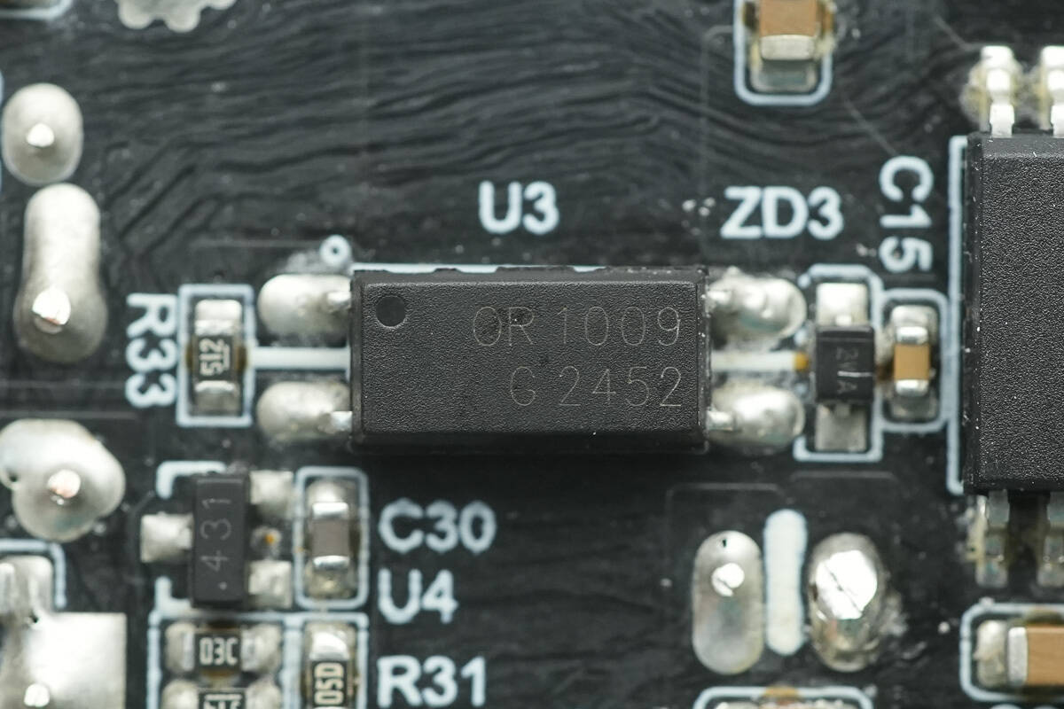
The OR1009 optocoupler is used for output voltage feedback.
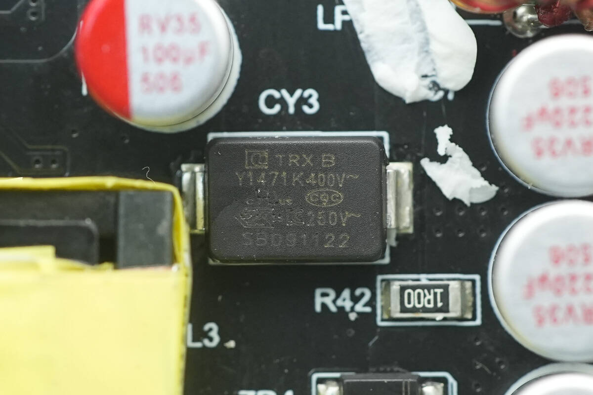
The SMD Y capacitor is from TRX. Its compact size and light weight make it well-suited for high-density power products such as GaN fast chargers. The part number is TMY1471K.
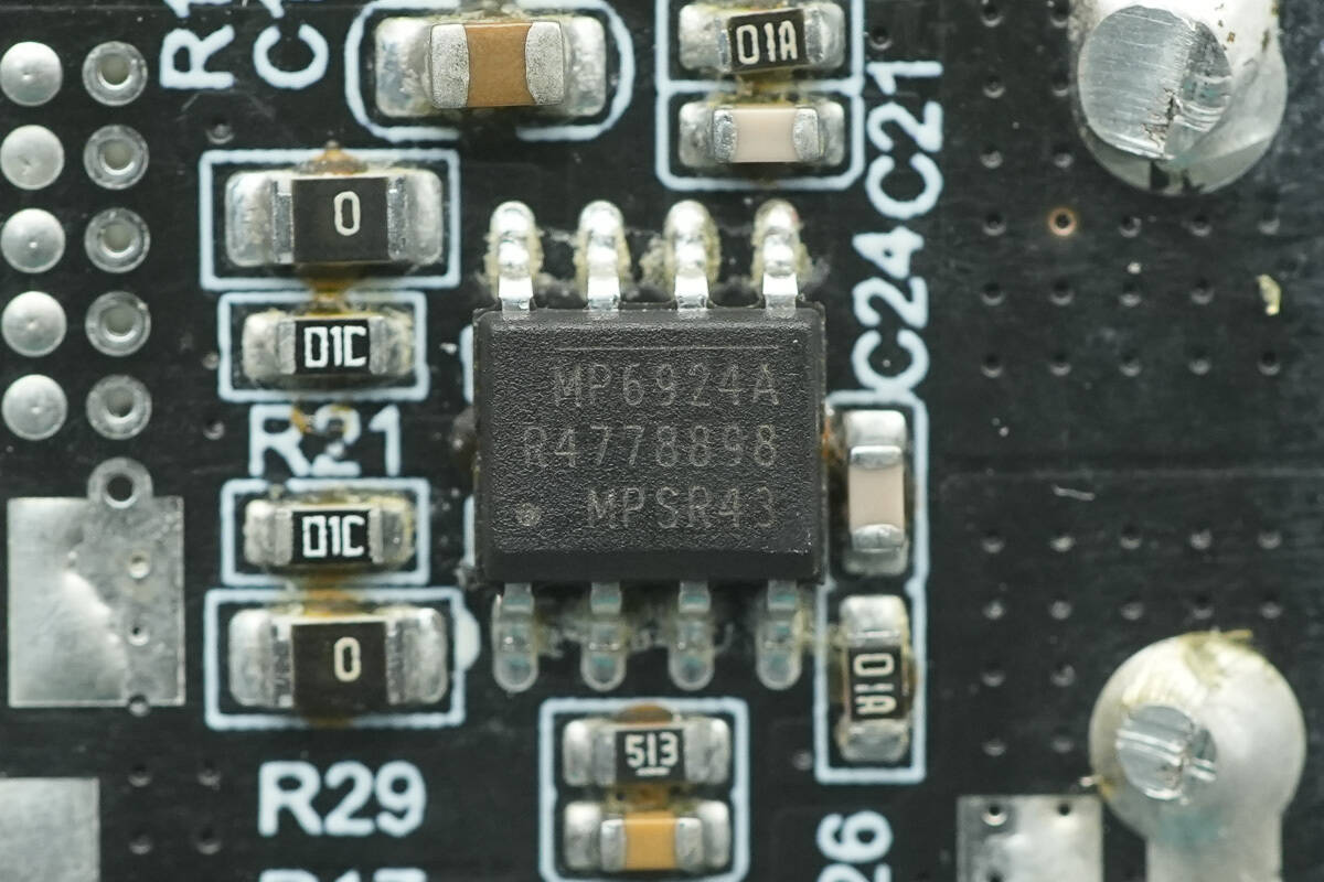
The synchronous rectifier controller is from MPS, model MP6924A. It is an LLC synchronous rectifier controller with enhanced interference immunity and fast turn-off functionality, compatible with both CCM and DCM modes. The MP6924A integrates two synchronous rectifier controllers internally, each designed for rectification applications on the two secondary windings of the LLC transformer. It is suitable for synchronous rectification applications in LLC converters and comes in an SOIC-8 package.
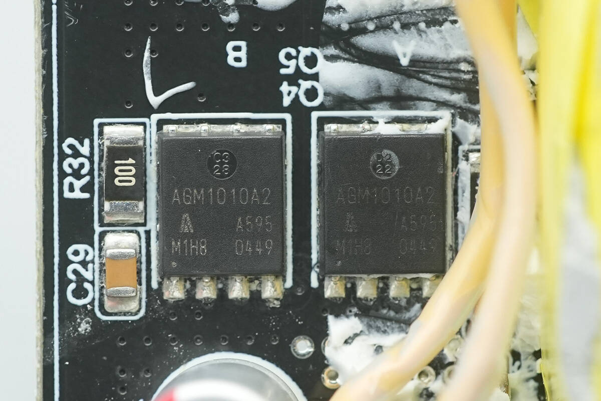
The synchronous rectifiers are from AGM-Semi, model AGM1010A2. They are NMOS transistors with a voltage rating of 100V and an on-resistance of 7.8mΩ. They come in a PDFN 5*6 package.
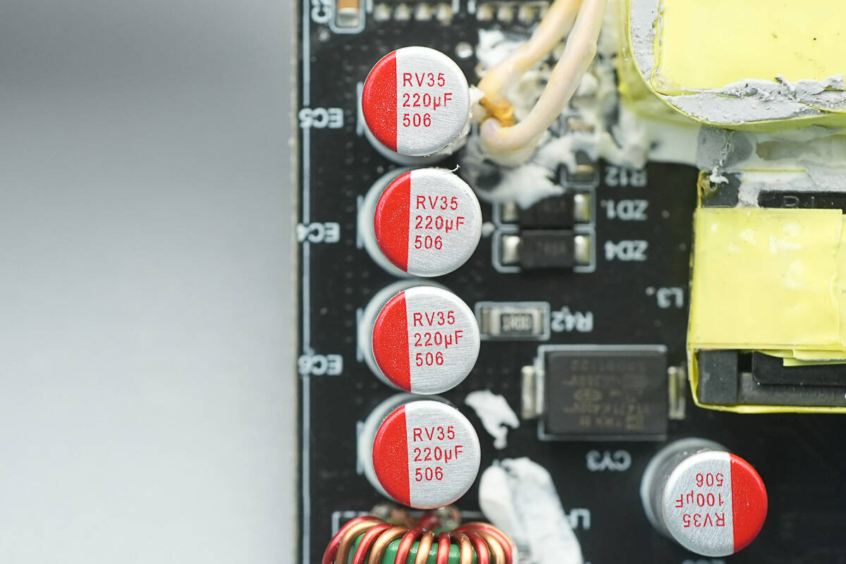
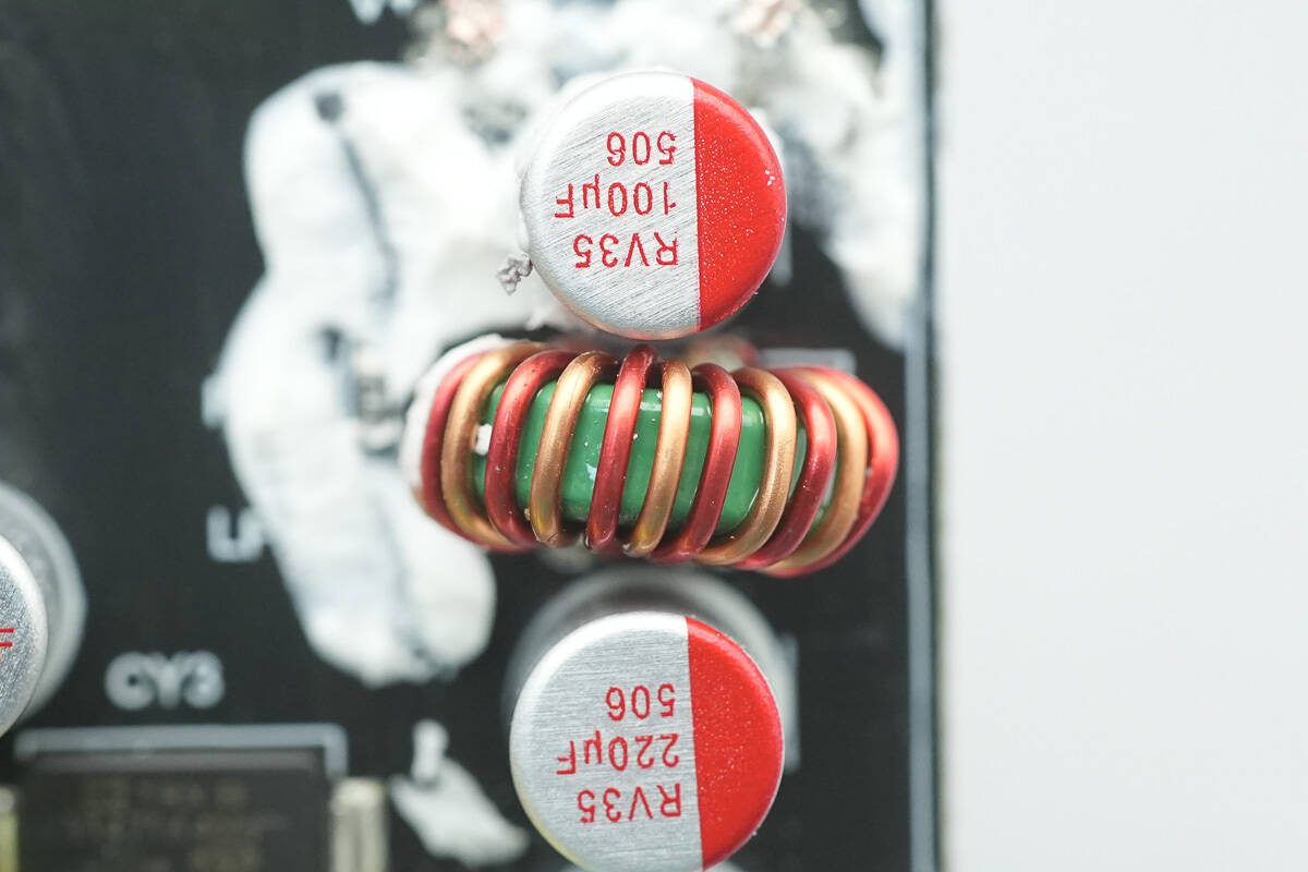
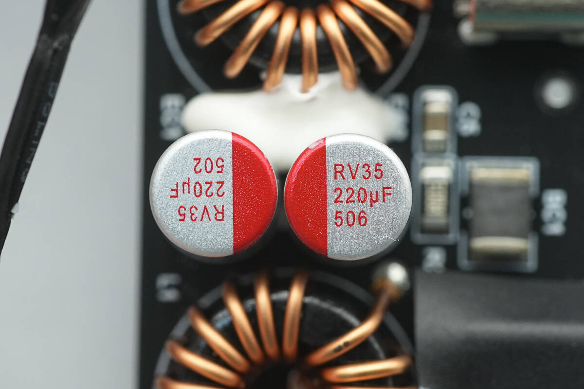
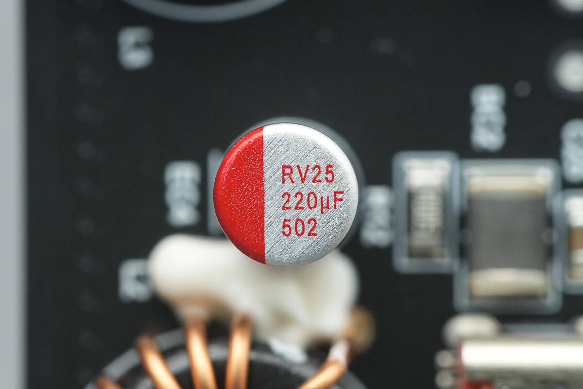
The four output filter solid capacitors all have a specification of 35V 220μF.
The fifth solid filter capacitor has a specification of 35V 100μF.
A close-up of the filter inductor.
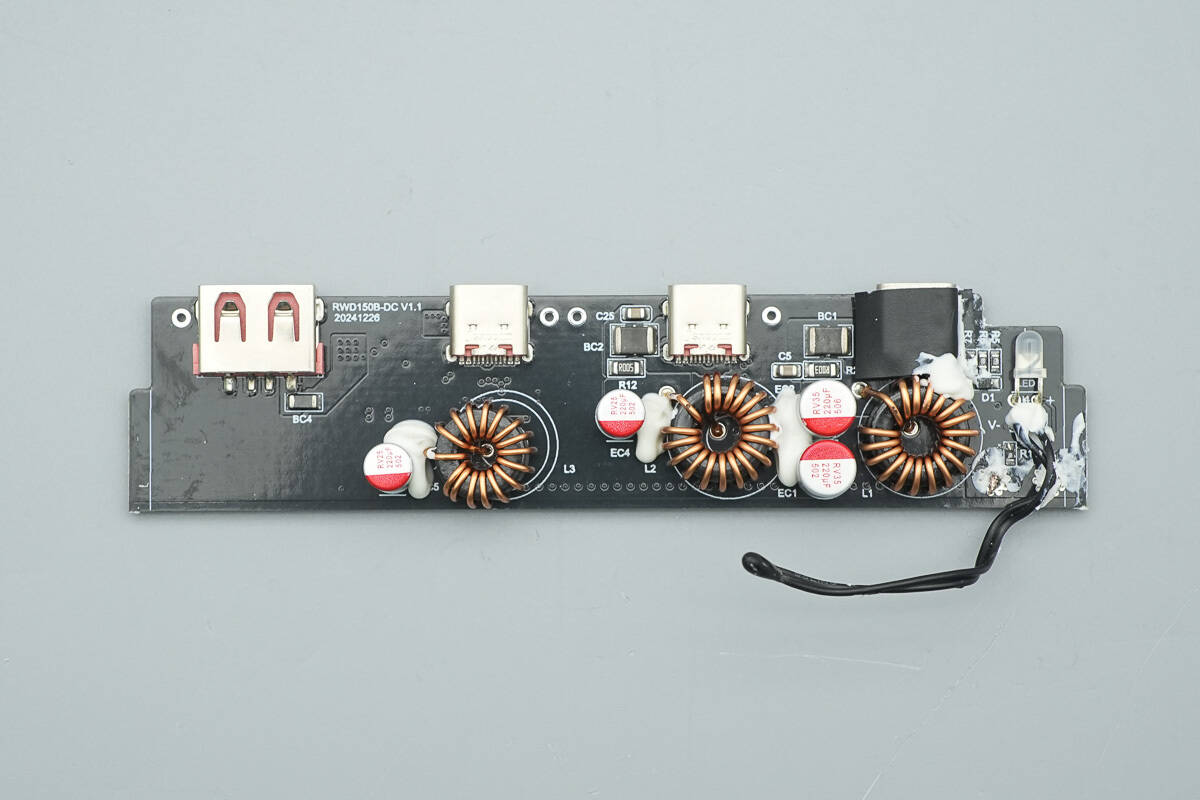
The front of the output PCB features an indicator light, thermistor, buck inductors, and solid-state capacitors.
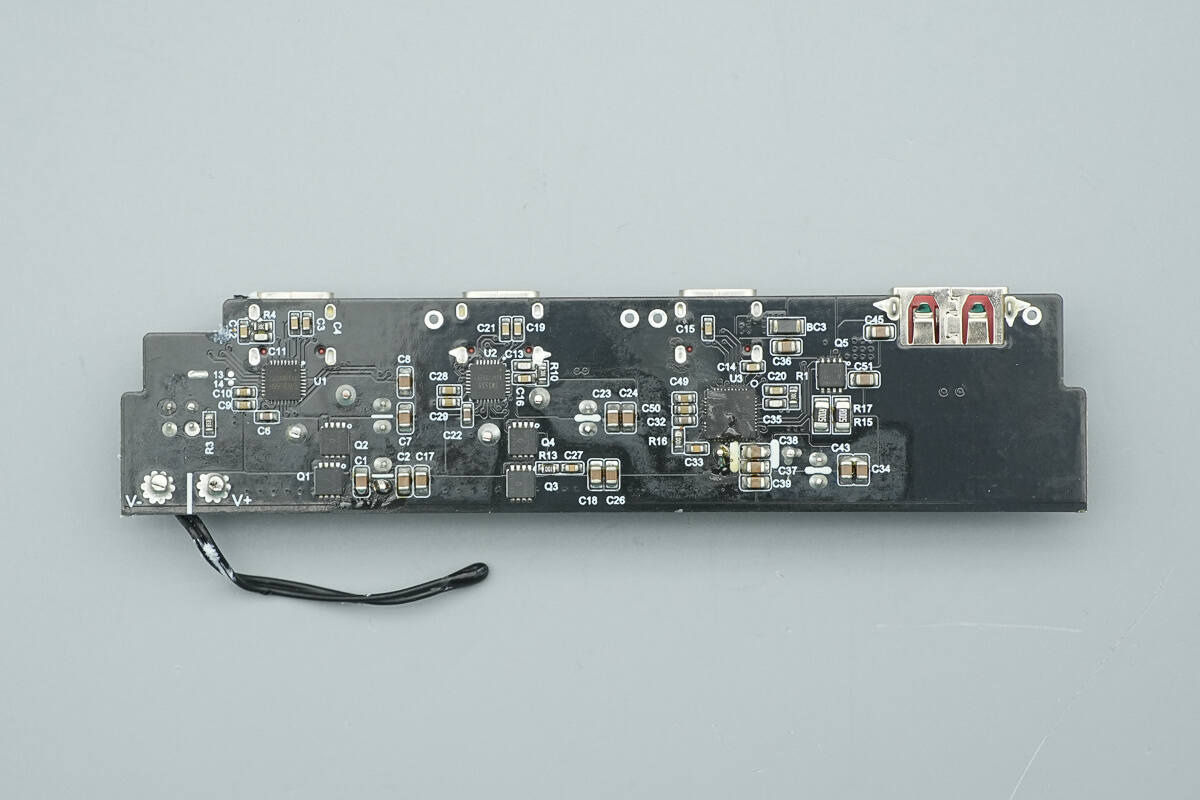
The back of the PCB contains buck protocol chips, synchronous buck MOSFETs, and a VBUS MOSFET.
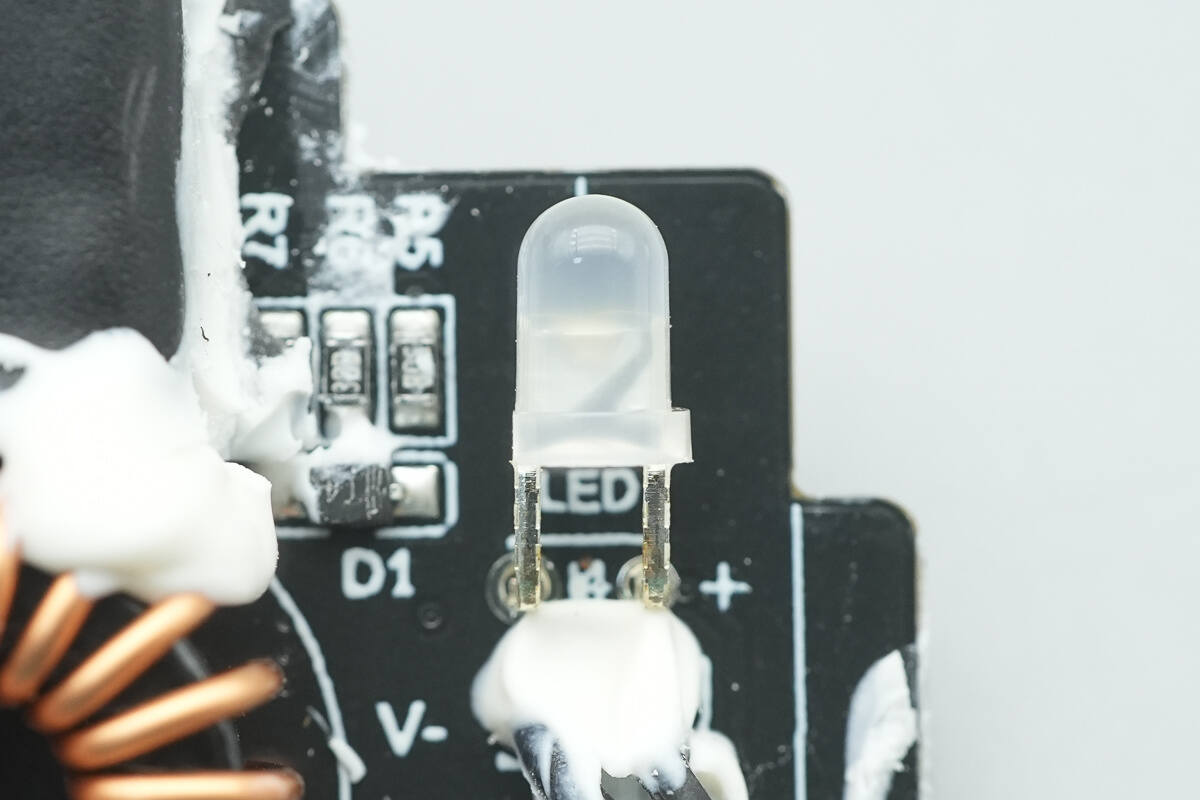
A close-up of the indicator light.
A close-up of the thermistor.
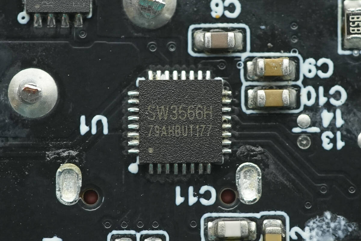
The buck protocol chip used for the USB-C1 interface is from iSmartWare, model SW3566H. It is a highly integrated dual-port fast charging SOC that supports USB-C and USB-A charging, with independent current limiting for both ports. It integrates a high-efficiency synchronous buck converter, supporting 20V7A and 28V5A outputs, and is compatible with fast charging protocols such as PD3.1, QC, SCP, UFCS, etc. It also supports custom fast charging protocols, with a maximum output power of 140W.
The SW3566H integrates CC/CV mode, dual-port management logic, and bus voltage detection. Paired with corresponding buck switching devices and VBUS MOSFETs, it can achieve dual-port buck output. The chip's built-in buck converter operates at a frequency of 180kHz, supporting both PWM and PFM modes. Output current, line loss compensation, and other protection thresholds can be set via the I2C interface. The built-in ADC allows data sampling of nine channels, including input/output voltage, output current, and chip temperature, and supports an external MCU for parameter display.
The SW3566H supports an input voltage of up to 36V and a maximum output current of 7A. The chip features built-in soft start, input overvoltage/undervoltage protection, output overvoltage/undervoltage protection, output overcurrent/short-circuit protection, DP/DM/CC overvoltage protection, chip overheat protection, external NTC thermistor protection, and power limiting protection. The chip is packaged in a QFN 4*4-32 form factor.
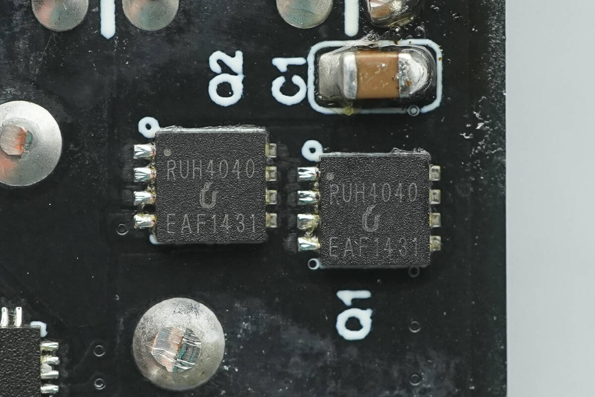
The two synchronous buck MOSFETs are from Ruichips, model RUH4040. They are NMOS transistors with a voltage rating of 40V and an on-resistance of 8mΩ. They come in a PDFN 3333 package.
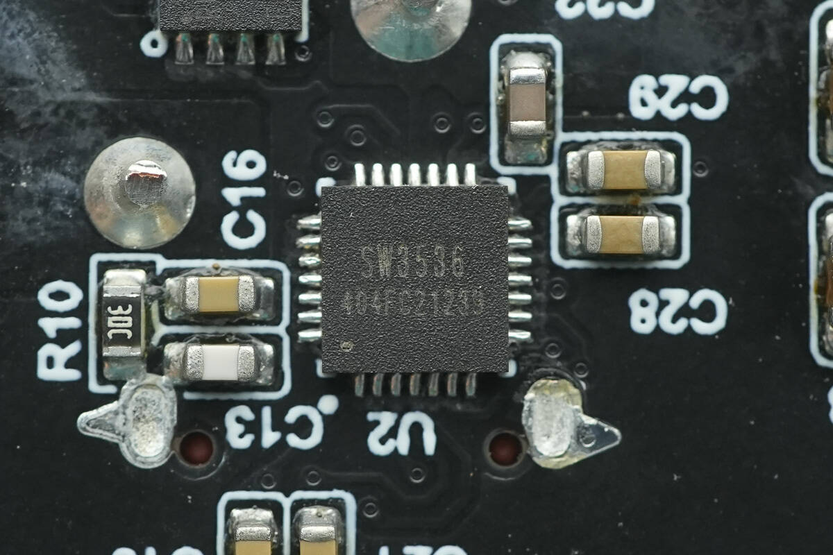
The buck protocol chip for the USB-C2 port is from iSmartWare, model SW3536. It is a highly integrated multi-protocol dual-port charging chip that supports USB-A + USB-C dual-port fast charging output with independent current limiting for both ports. It integrates a 7A high-efficiency synchronous buck converter and supports multiple fast charging protocols, including PPS, PD, QC, AFC, FCP, SCP, PE, SFCP, and TFCP. The chip supports a maximum output power of 140W.
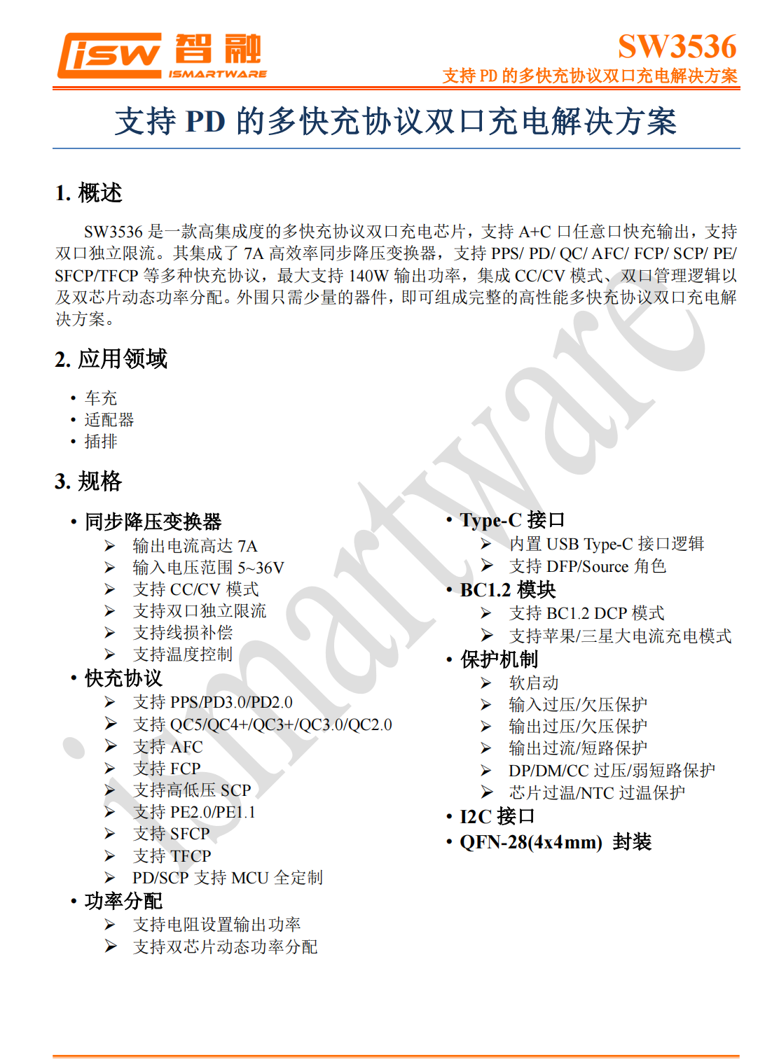
The SW3536 integrates CC/CV mode, dual-port management logic, and dynamic power distribution between two chips, with a simplified set of external components. It provides a complete, high-performance multi-protocol dual-port charging solution. The SW3536 supports an input voltage of up to 36V, making it suitable for 12-24V input car charging applications. It is ideal for fast charging adapters, power strips, and car charger applications.
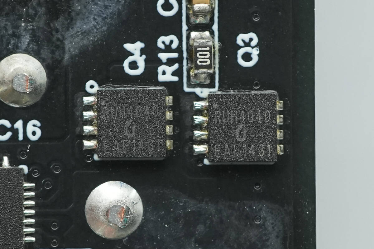
These two synchronous buck MOSFETs are also Ruichips RUH4040.
A close-up of the buck inductors used in the two buck conversion circuits, with the USB-C1 socket wrapped in insulating tape.
The two solid capacitors used for synchronous buck output filtering on the USB-C1 port have a specification of 35V 220μF.
The solid capacitor used for the USB-C2 port has a specification of 25V 220μF.
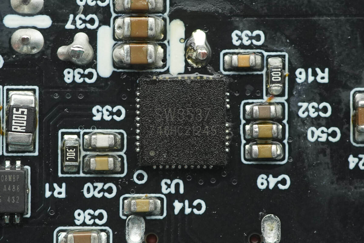
The buck protocol chip used for the USB-C3 and USB-A ports is from iSmartWare, model SW3537. It integrates a 5A high-efficiency synchronous rectifier buck converter and supports multiple charging protocols, including PPS, PD, QC, AFC, FCP, SCP, PE, SFCP, and low-voltage direct charging. It also supports CC/CV mode. Only a few external components are needed to form a complete, high-performance multi-protocol dual-port charging solution.
Thanks to the chip's high integration, the SW3537 combines the protocol chip, synchronous buck controller, and buck MOSFET all in one package, greatly simplifying the circuit design for multi-port fast charging. The chip supports A+C dual-port fast charging applications and includes comprehensive protection features.
Here is the information about iSmartWare SW3537.
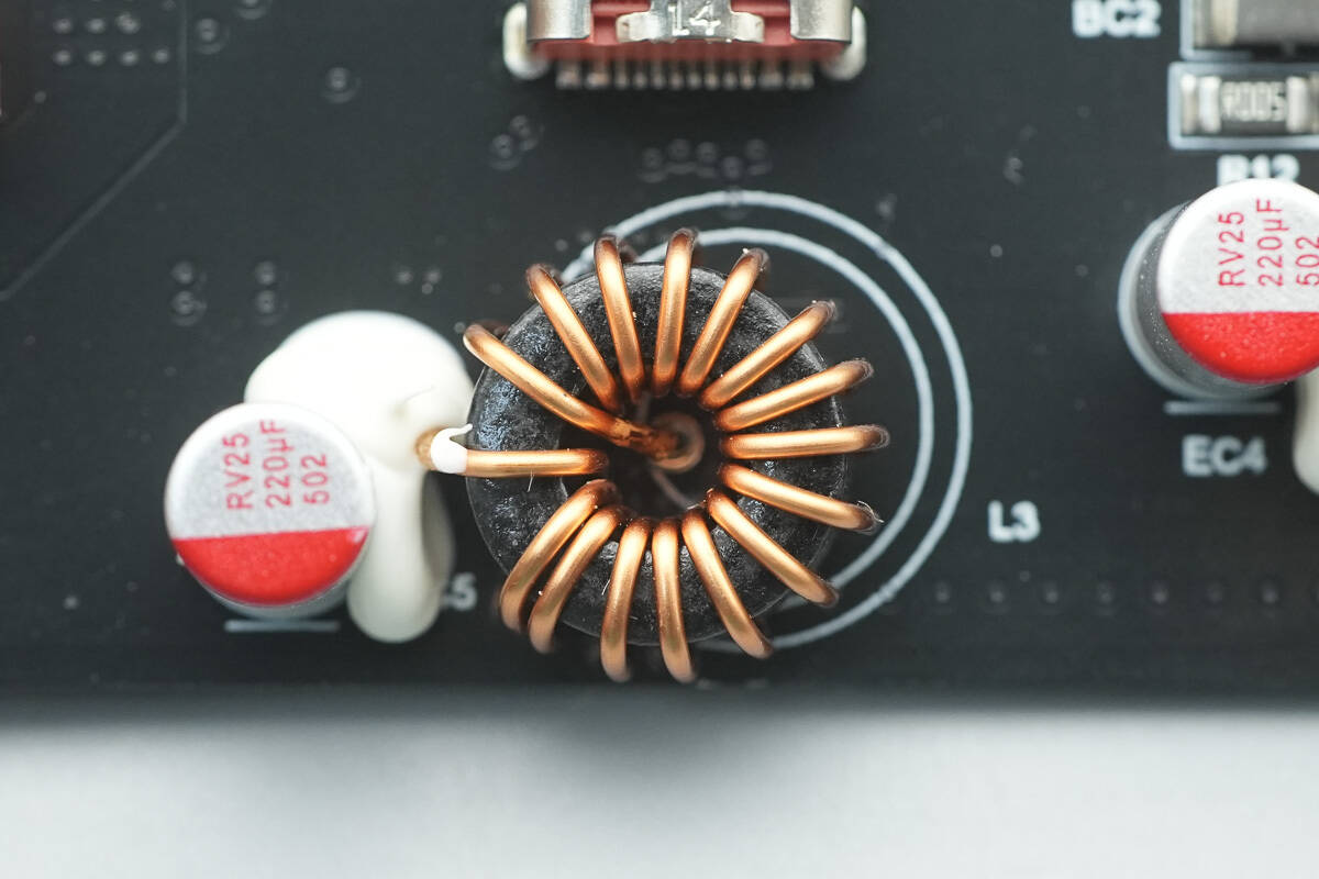
A close-up of the buck inductors used in the system.
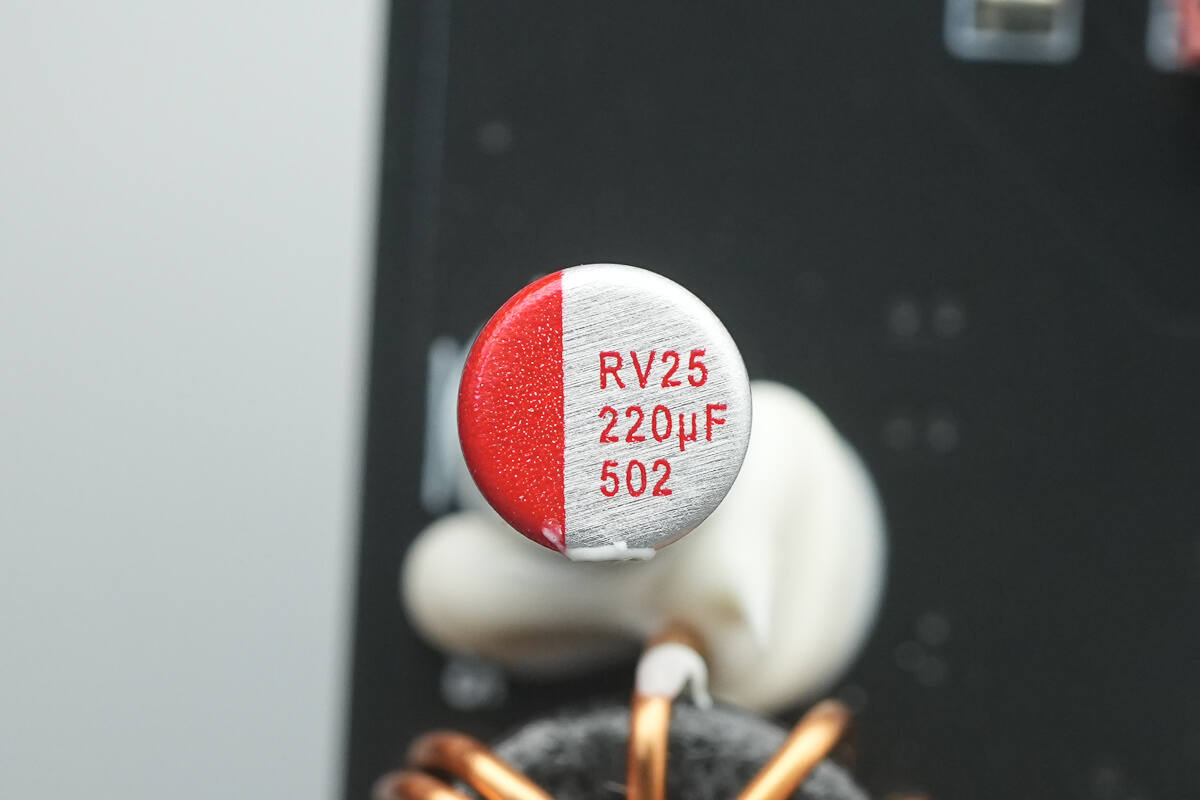
The solid capacitor for the buck output has a specification of 25V 220μF.
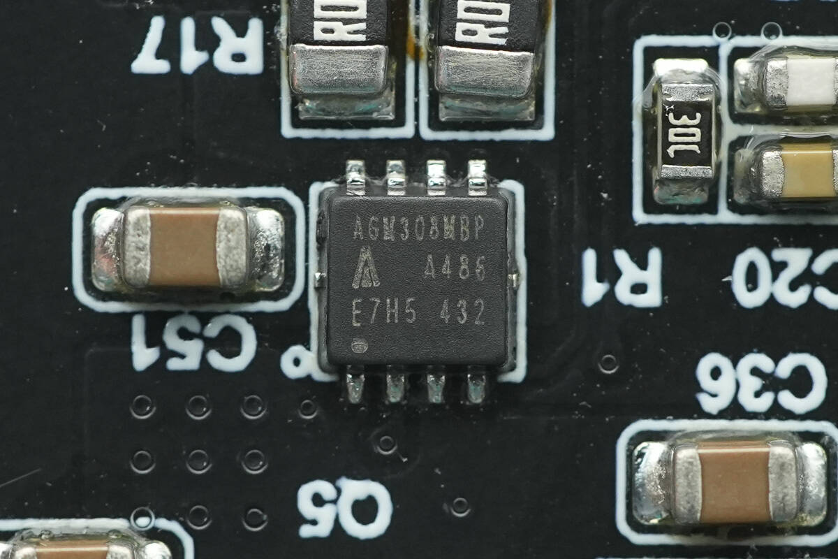
The VBUS MOSFET is from AGM-Semi, model AGM308MBP. It is a dual NMOS with a voltage rating of 30V and an on-resistance of 7mΩ. It comes in a PDFN 3*3 package.
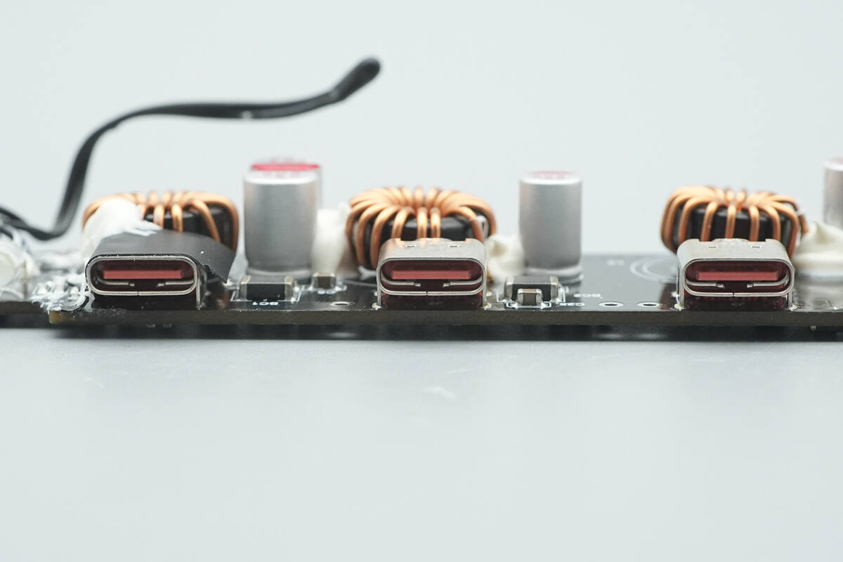
A close-up of the three USB-C sockets.
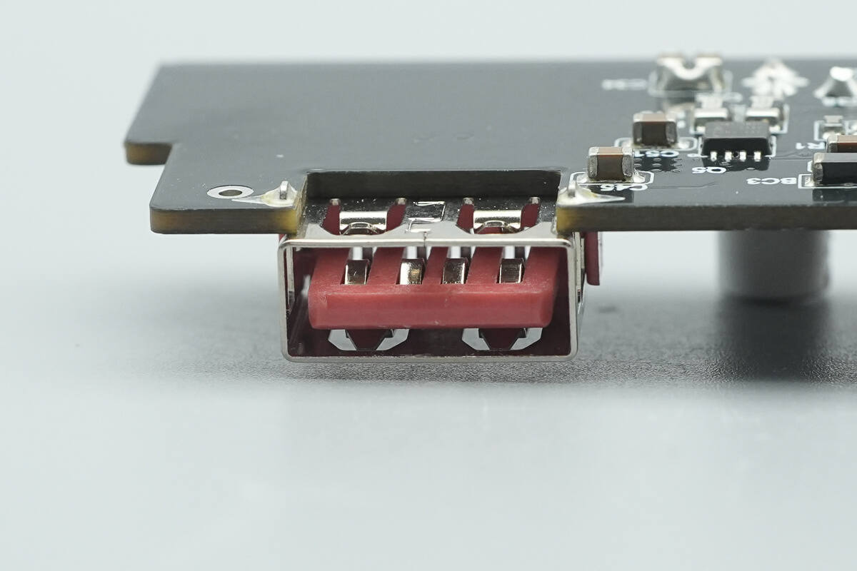
A close-up of the USB-A sockets.
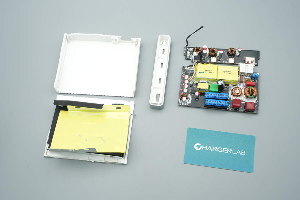
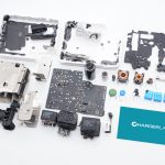
Well, those are all components of the MOVESPEED 165W GaN Desktop Charger.
Summary of ChargerLAB
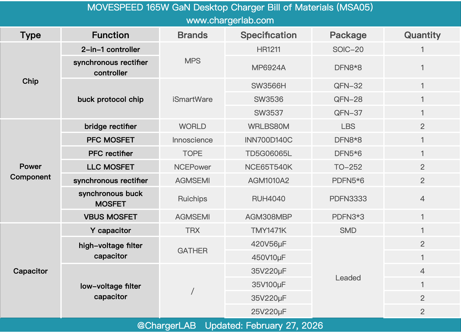
Here is the component list of the MOVESPEED 165W GaN Desktop Charger for your convenience.
It is equipped with 3 USB-C ports and 1 USB-A port, supporting multiple power output levels of 140W, 100W, 45W, and 30W, meeting the charging needs of various devices such as laptops, tablets, smartphones, and gaming consoles simultaneously.
After taking it apart, we found that it uses the MPS HR1211 two-in-one controller paired with the Innoscience INN700D140C GaN FET for a high-performance PFC+LLC power architecture. The PFC rectifier utilizes the TOPE TD5G06065L silicon carbide Schottky diode, while the LLC MOSFETs are from NCEPower, model NCE65T540K. The synchronous rectifier controller is the MPS MP6924A, paired with AGM-Semi AGM1010A2 synchronous rectifiers.
The output uses a three-channel independent buck conversion scheme, with the iSmartWare SW3566H, SW3536, and SW3537 buck protocol chips for each port, enabling independent fast charging output and intelligent power distribution. The PCBA module is filled with a large amount of thermal adhesive, paired with a large heat sink to enhance heat dissipation. The use of solid and reliable materials ensures the stability and charging compatibility of the charger.
Related Articles:
1. Teardown of Belkin 112W 4-Port GaN Charger (WCH017yz)
2. Teardown of Meizu PANDAER 66W Vertical Air-cooled Wireless Charger (WP06)
3. Teardown of VERTIV 3500W SiC Rectifier Module (R48-3500e3)