Introduction
Previously, we shared our review of the Lenovo Legion Go S, highlighting its impressive specs like the exclusive AMD Z2 Go APU based on Zen 3+ architecture, a stunning PURESIGHT display, and dual USB4 ports—all packed into a sleek handheld design. Rather than revisit the performance details, today we’re taking a different approach: a full teardown of the Legion Go S. Let’s dive inside and see how Lenovo has engineered this compact gaming console from the inside out.
Product Appearance
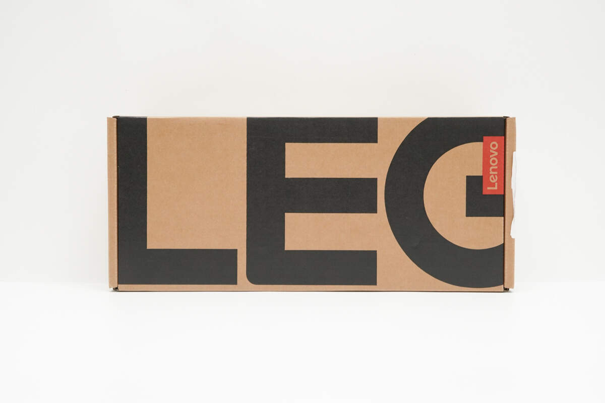
The Lenovo logo is printed on the right side of the box.
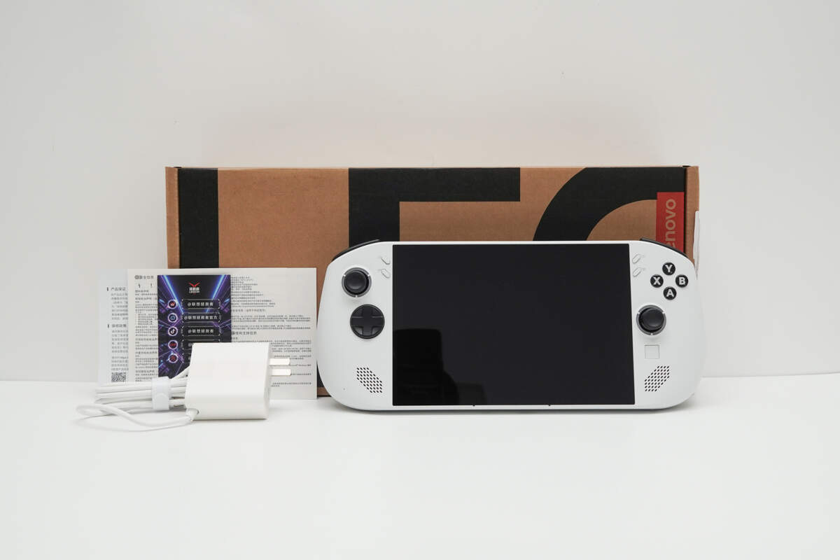
The box contains the Lenovo Legion Go S, an adapter, and some documents.
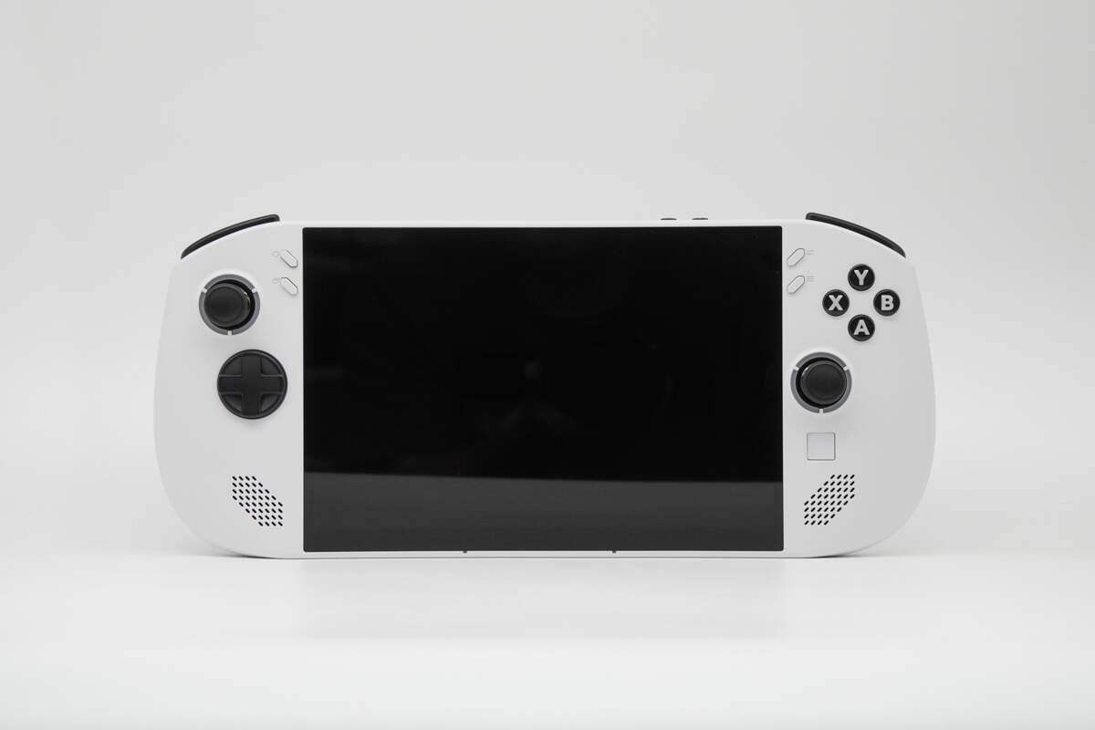
The Lenovo Legion Go S abandons the detachable controller design seen in the Legion Go, which is similar to the Switch, and instead adopts an integrated design. Its corners are rounded, and the overall lines are smooth, ensuring that extended use does not result in discomfort.
In Beast Mode, airflow is increased by 68%, effectively reducing the device’s temperature and ensuring stability during high-performance gaming. In Silent Mode, noise levels drop as low as 25dB(A), allowing for quiet gameplay even late at night without disturbing others.
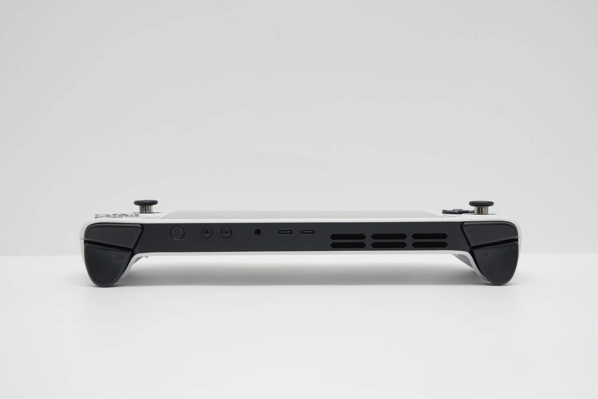
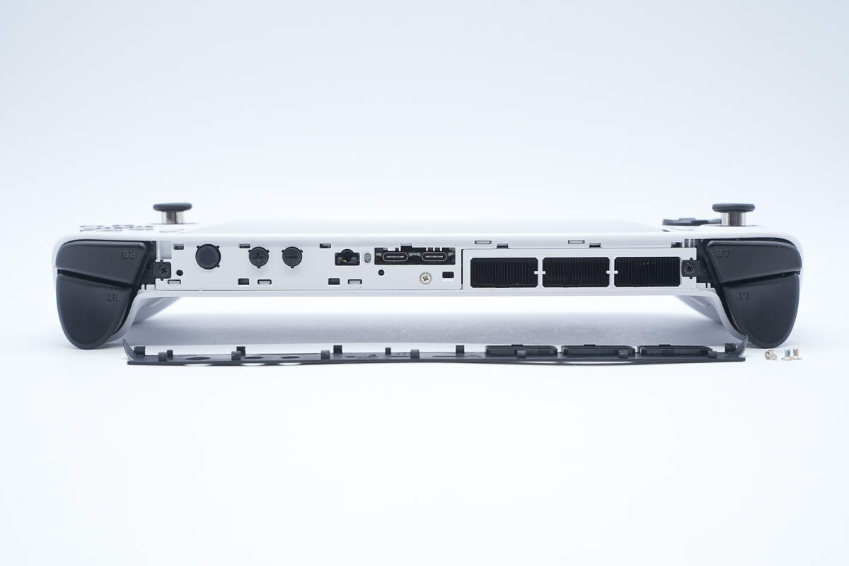
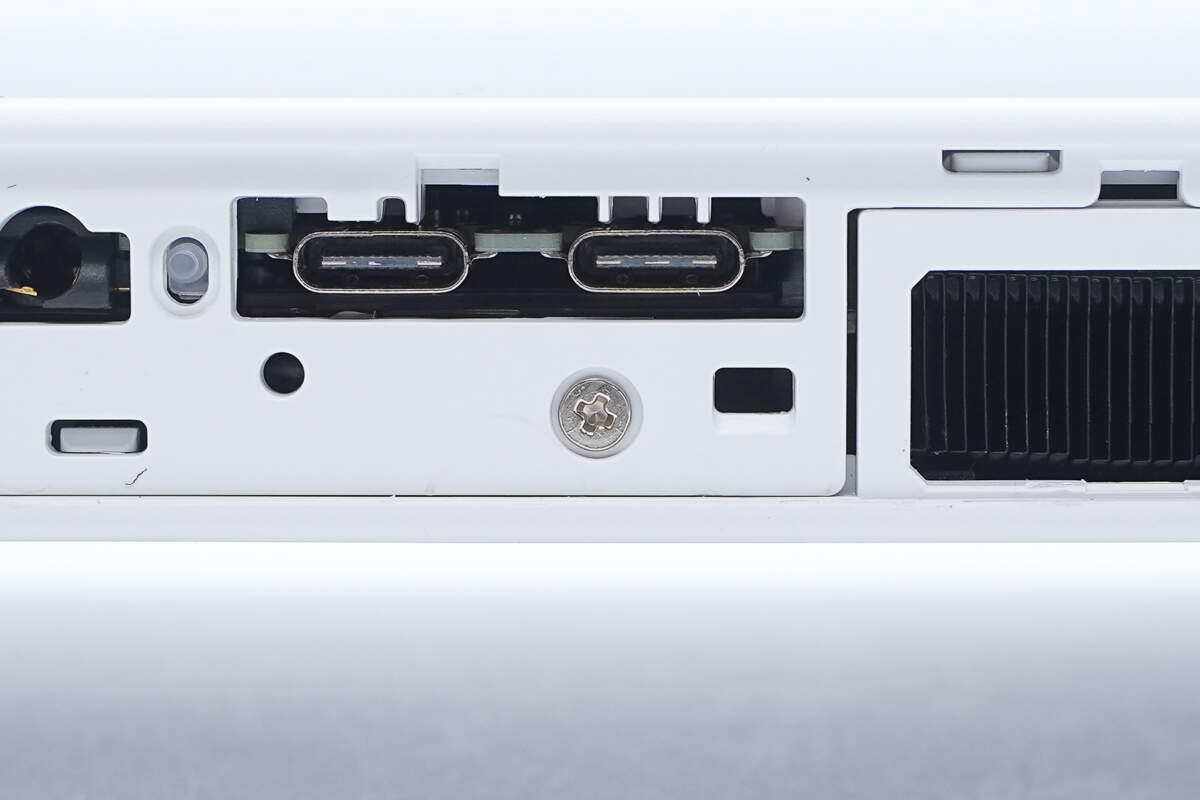
It is equipped with two USB-C ports on the top, both conforming to the USB4 standard. These ports support PD 100W charging, 4K 120Hz video output, and data transfer rates of up to 40 Gbps.
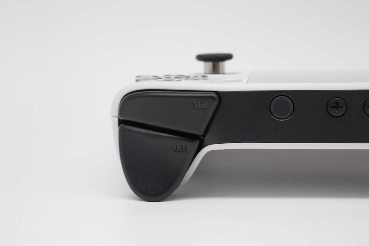
Both sides of the top feature adjustable two-stage Hall trigger designs. The pressure and damping feel are highly responsive, allowing for more precise control during gameplay.
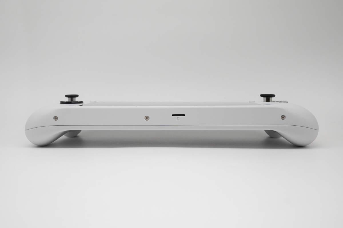
The bottom features an SD card slot with a maximum capacity of 2TB, and it also supports 2280 NVMe SSD expansion.
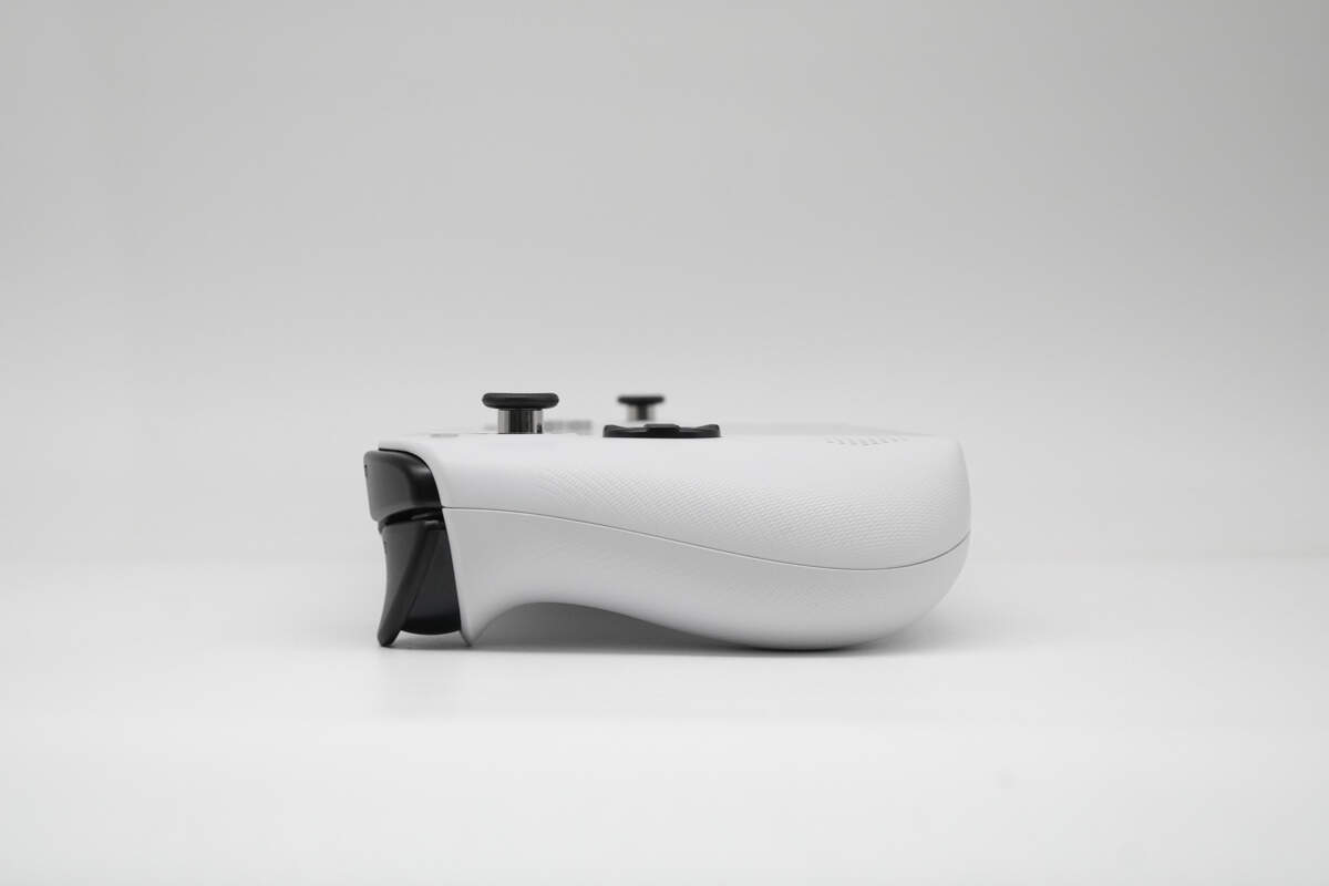
The overall design follows an ergonomic structure, with the thicker handles providing a fuller, more comfortable grip.
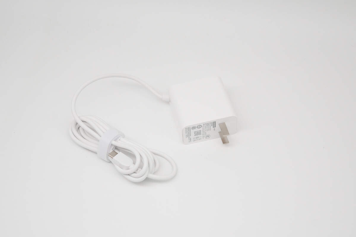
It comes with a 65W adapter with an integrated USB-C cable and a fine-grained frosted surface for a delicate touch.
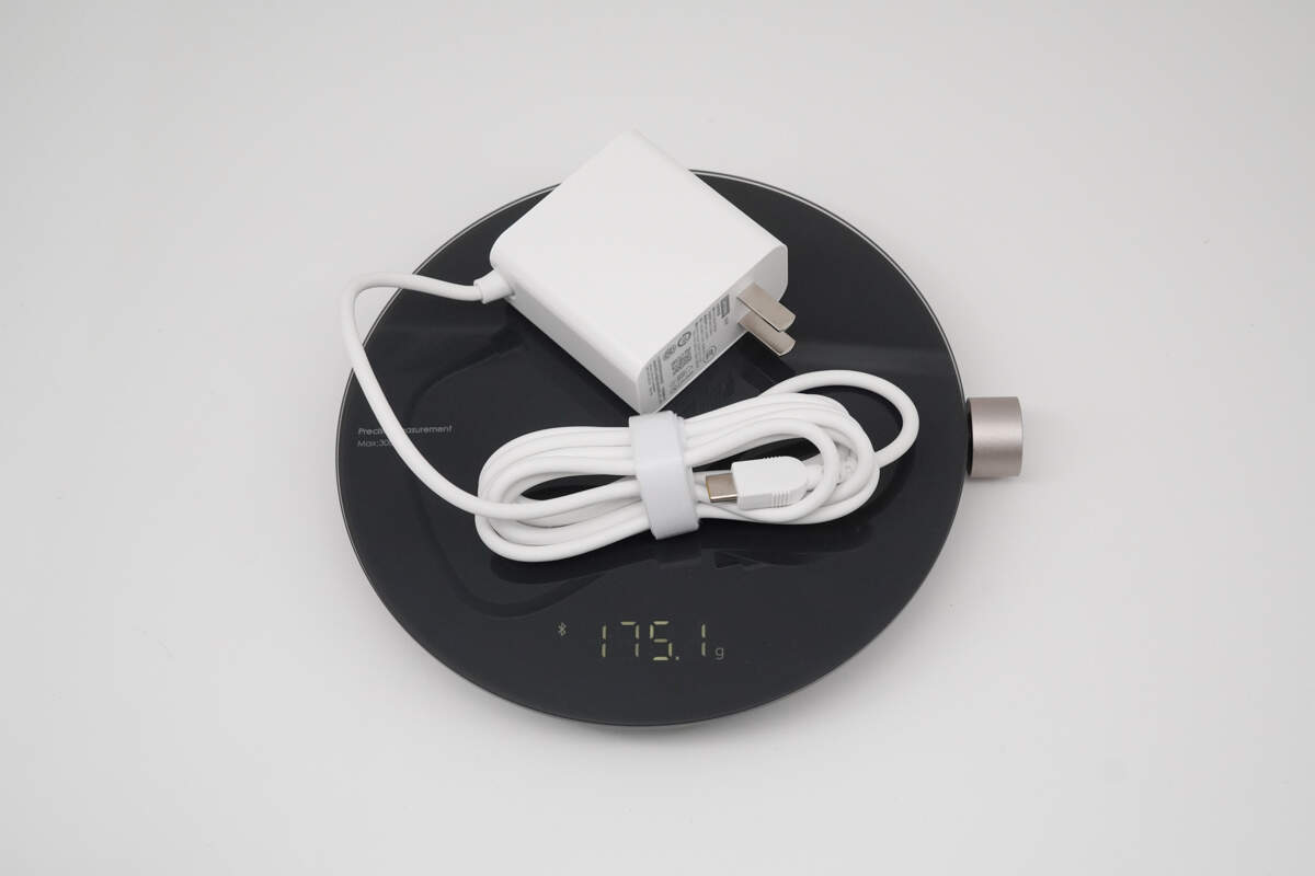
The weight is about 175 g (6.17 oz)
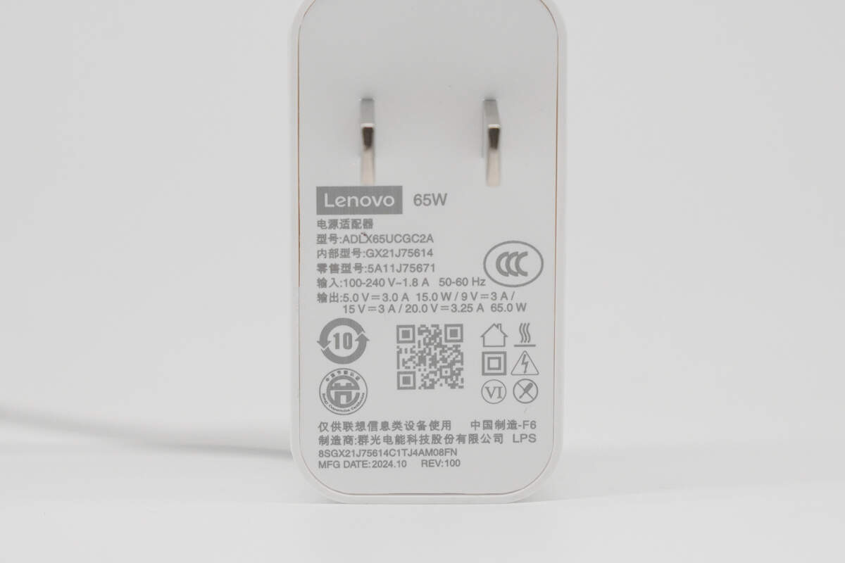
Model: ADLX65UCGC2A
Input: 100-240V-1.8A 50-60 Hz
Output: 5.0V3.0A 15.0W / 9V3A / 15V3A / 20.0V3.25A 65.0W
It has passed CCC, VI-level energy efficiency, and other certifications.
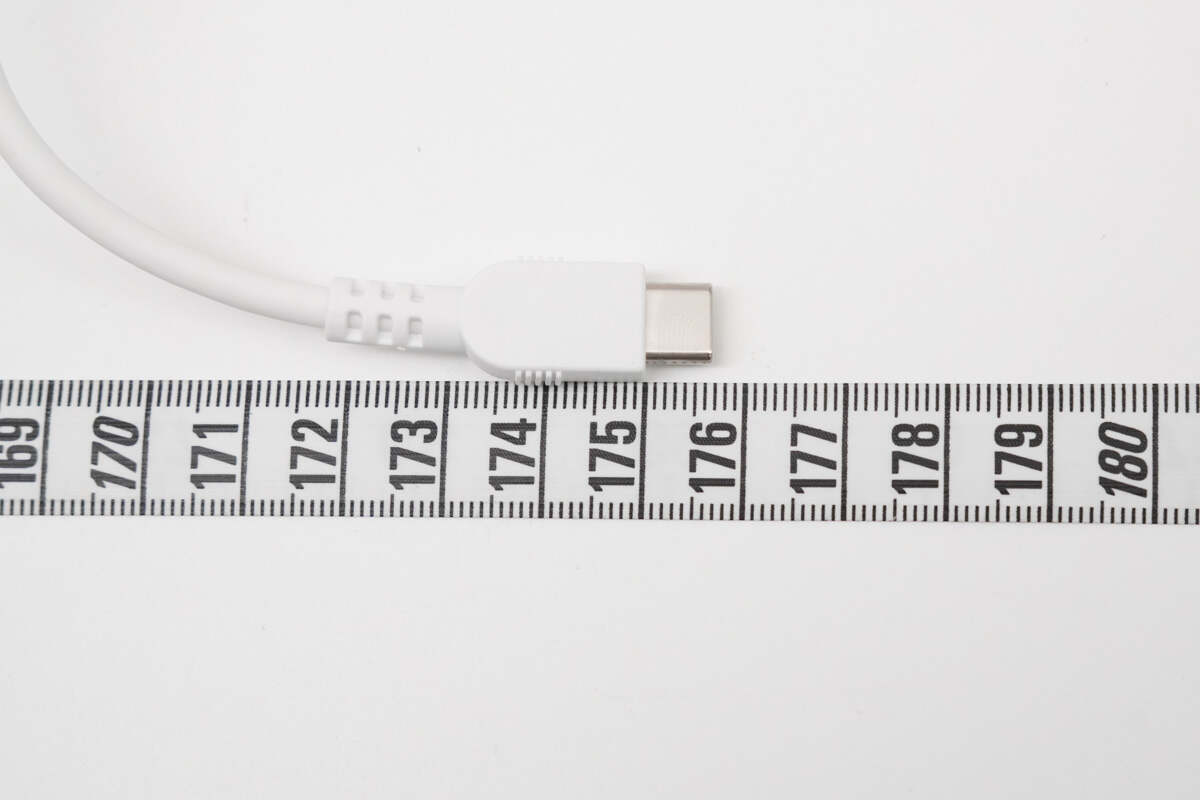
The length of the cable is about 176 cm (69.29 inches).
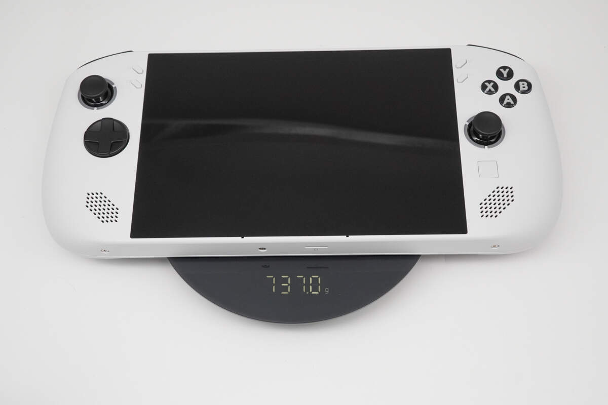
The weight of the gaming console is about 737 g (26 oz).
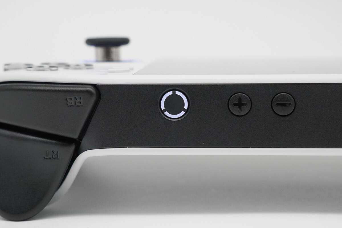
After turning on, the white indicator lights around the power button light up.
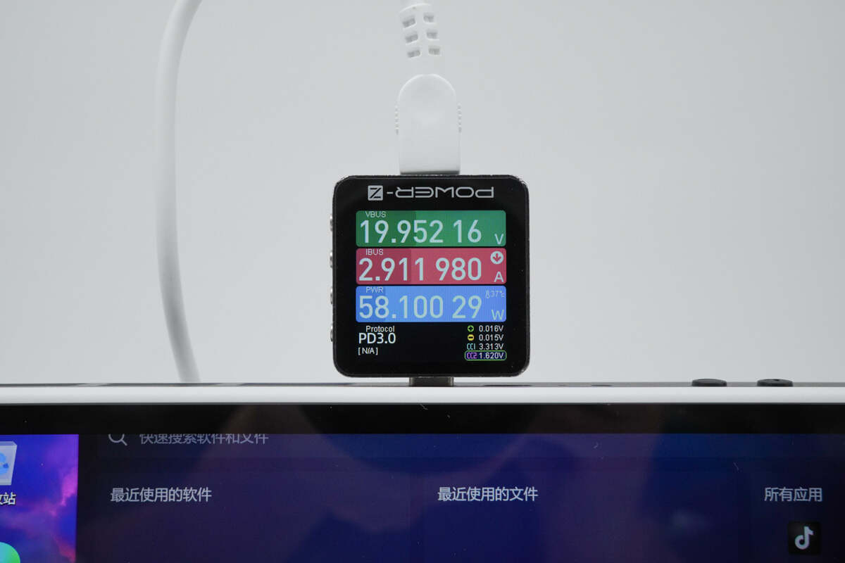
ChargerLAB POWER-Z KM003C shows the voltage is 19.95V, the current is 2.91A, and the power is about 58.1W.
Teardown
Next, let's take it apart to see its internal components and structure.
First, pry off the top cover.
This is the screw that holds the case in place.
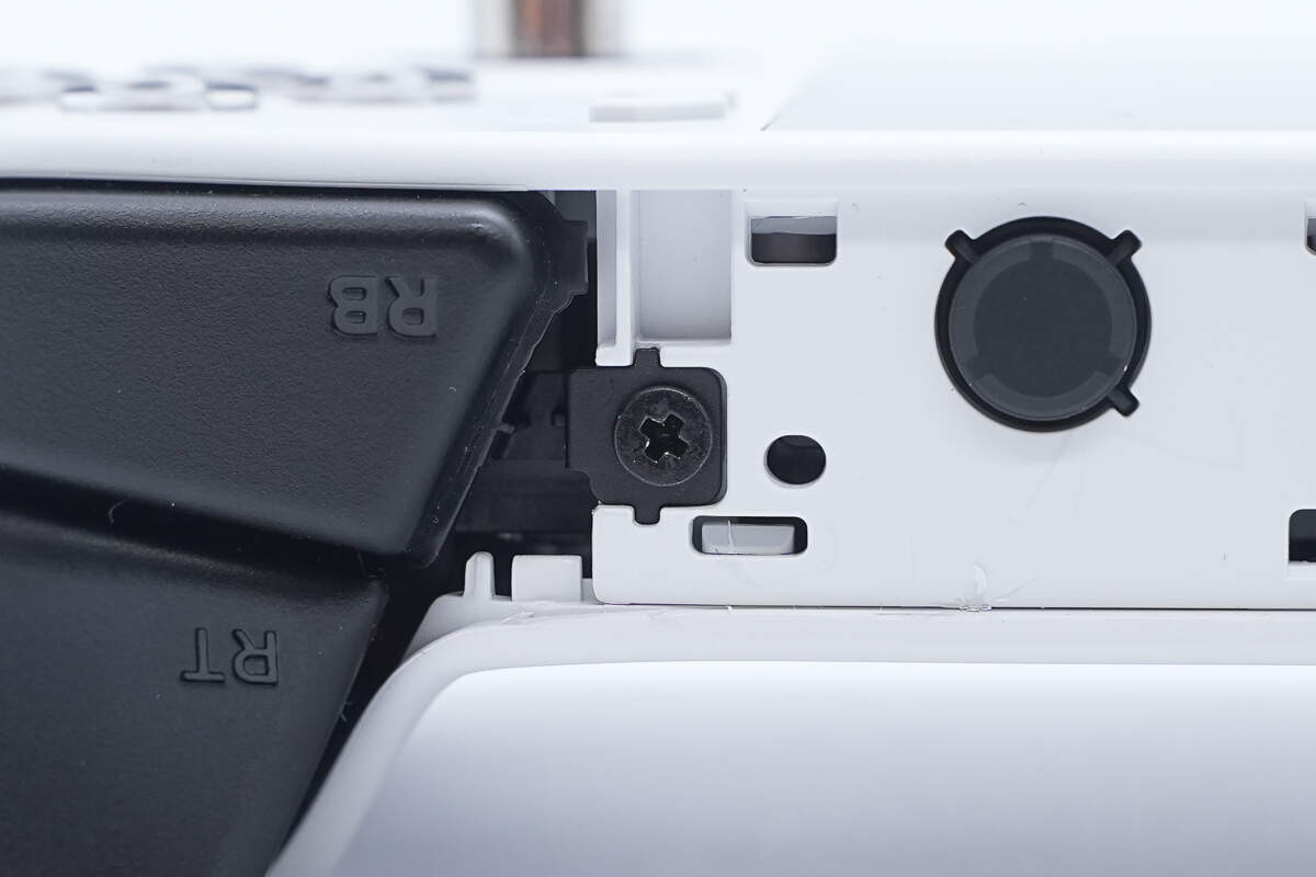
The shoulder buttons are also secured with screws.
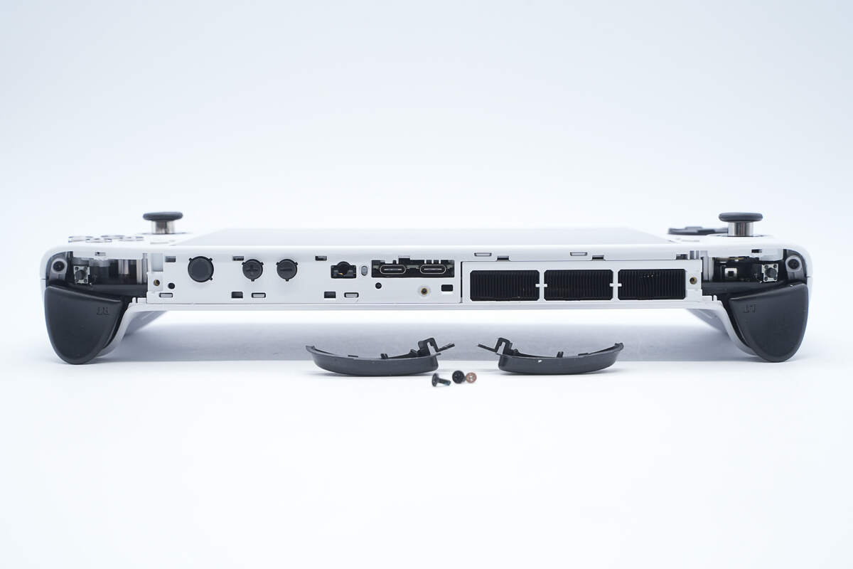
Unscrew the screws and remove the shoulder buttons. There are also fixing screws inside.
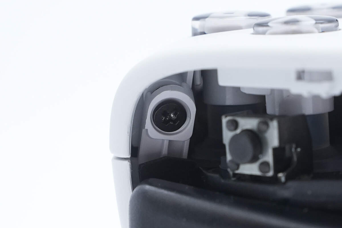
A close-up of the screws used to secure the case.
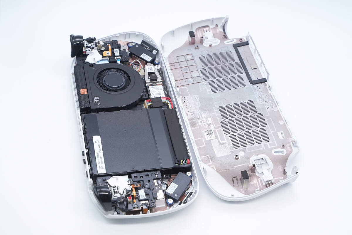
Remove the screws and open the outer case.
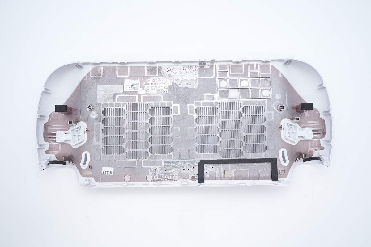
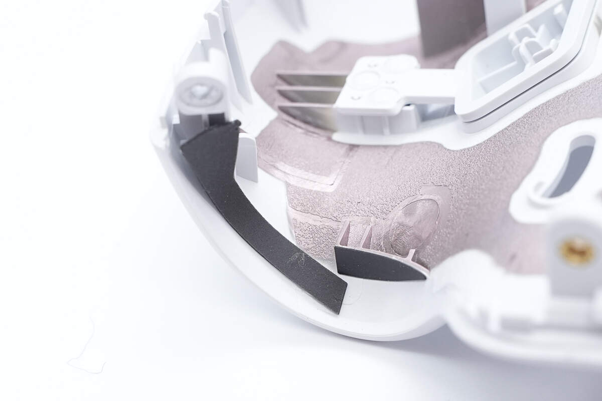
The inner side of the case has a shielding coating.
There is a button support structure inside.
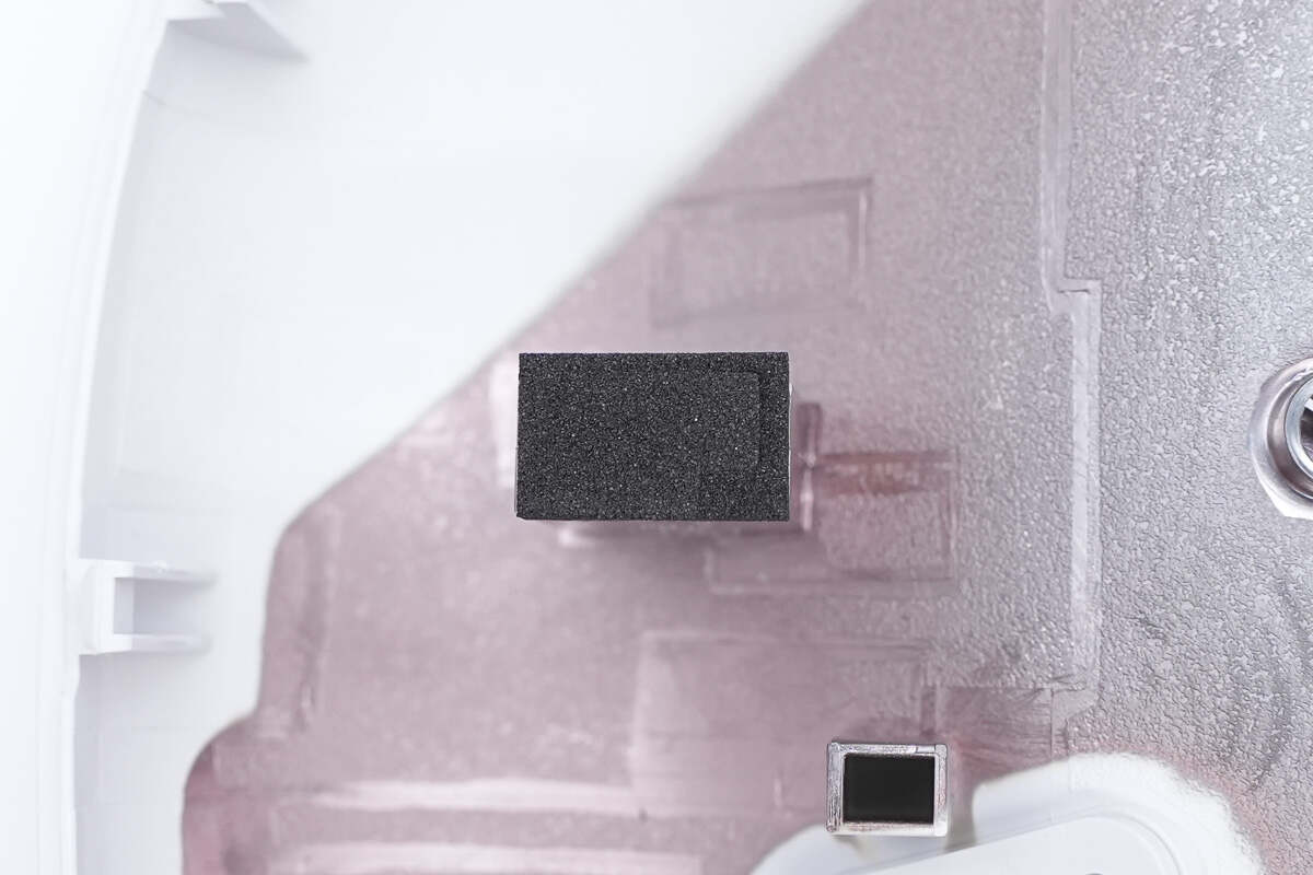
Cushioning foam is applied at the shoulder button area.
Foam sealing is applied around the heatsink area, along with conductive fabric for grounding purposes.
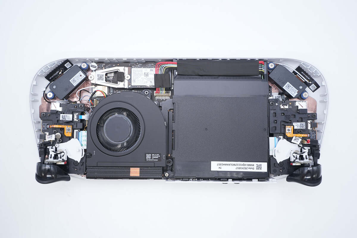
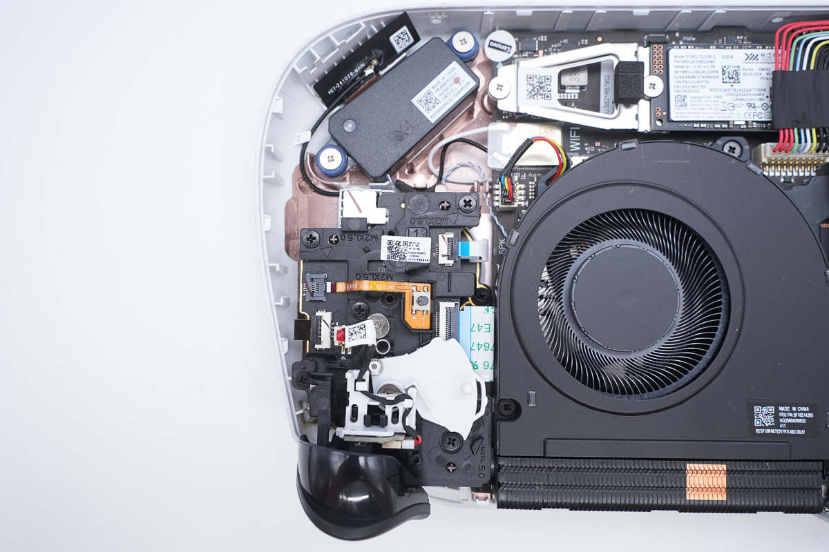
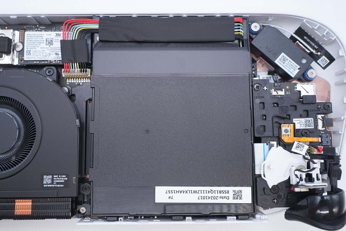
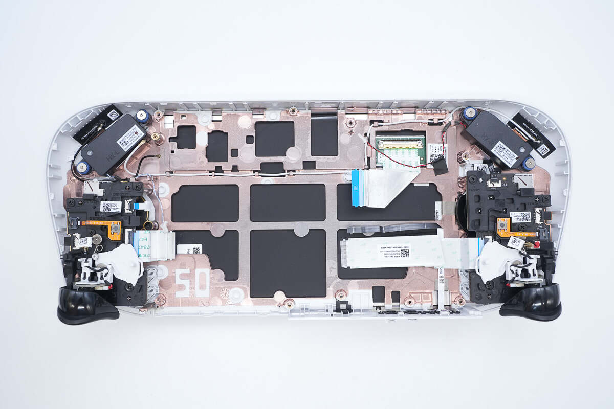
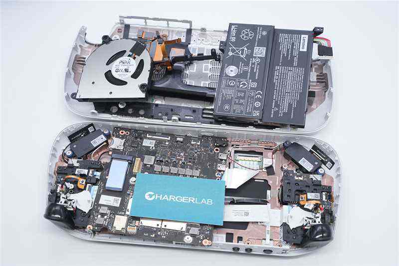
Inside, the cooling fan is positioned on the left side, with the SSD located above it. The battery pack is housed on the right side.
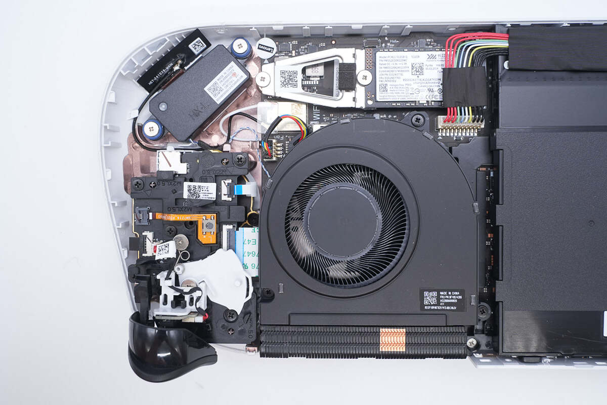
The cooling fan is connected via wires and secured in place with screws. The battery pack is also connected through wires.
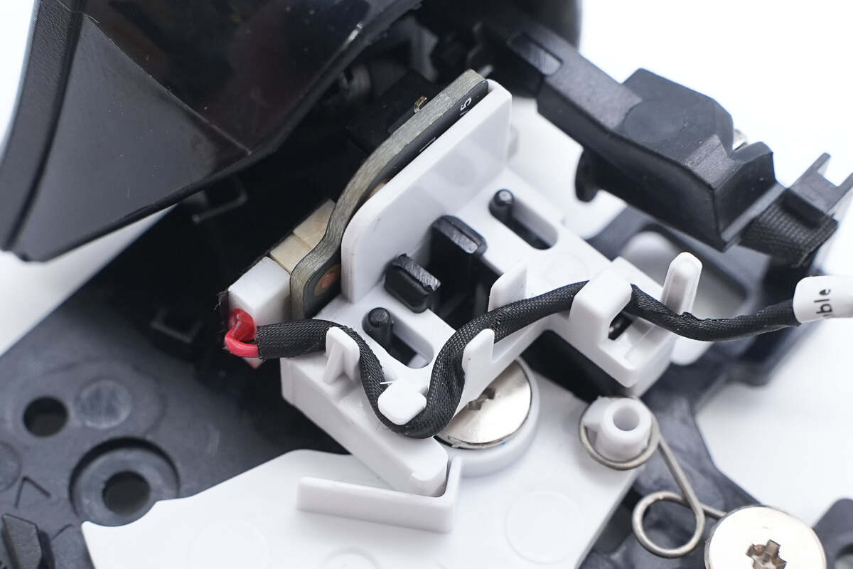
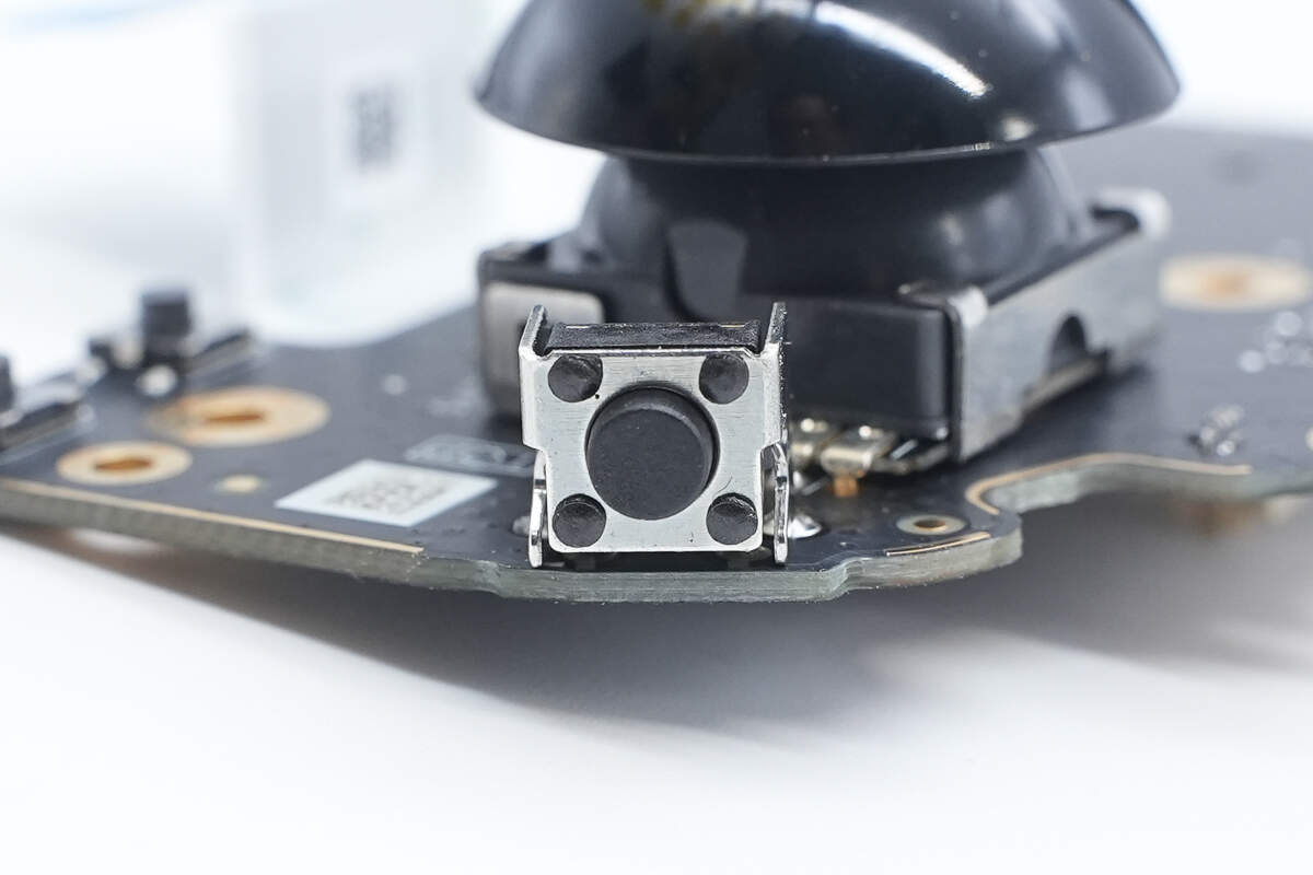
The buttons and joysticks are secured with screws.
This connector links the ribbon cable responsible for powering the RGB LED lights.
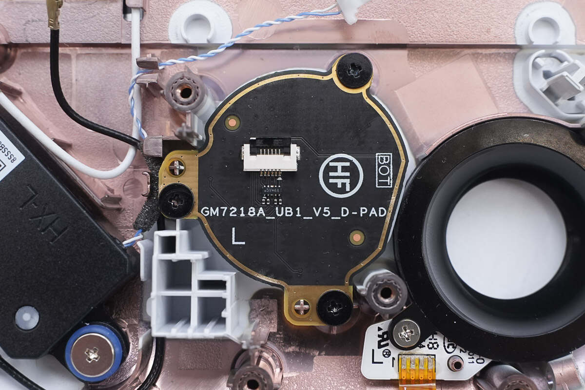
Close-up of the ribbon cable for the directional buttons.
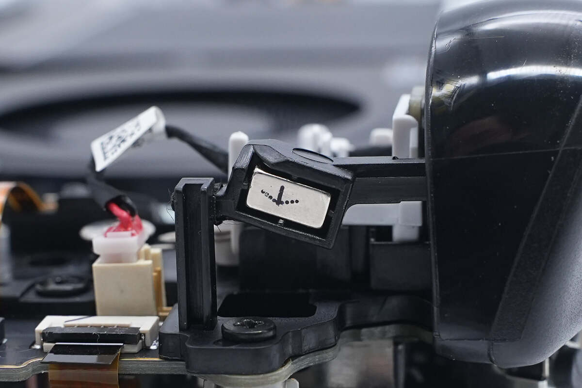
Close-up of the magnet for the Hall-effect trigger.
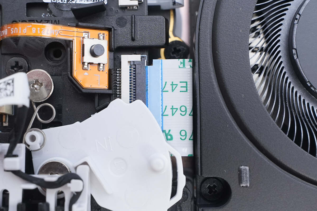
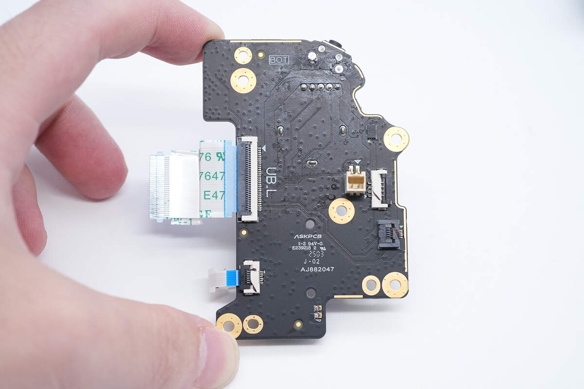
The secondary board is connected to the mainboard via a ribbon cable.
The speaker is secured with screws.
The WiFi antenna is secured inside the case.
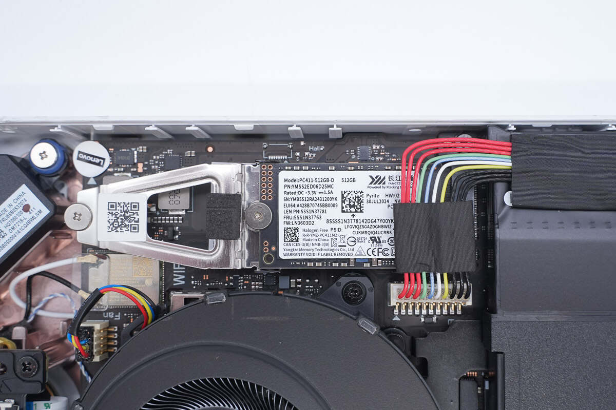
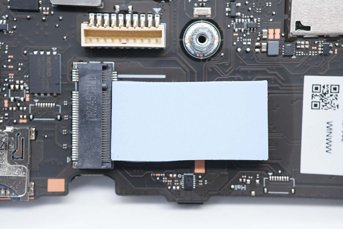
The SSD is a 2242 form factor and is secured using an extension board.
The battery pack is secured with screws.
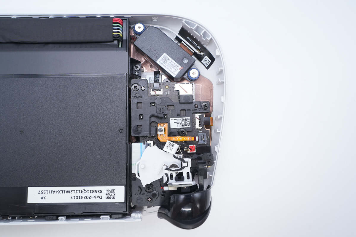
On the other side, there is also a joystick mechanism, speaker, and a WiFi antenna.
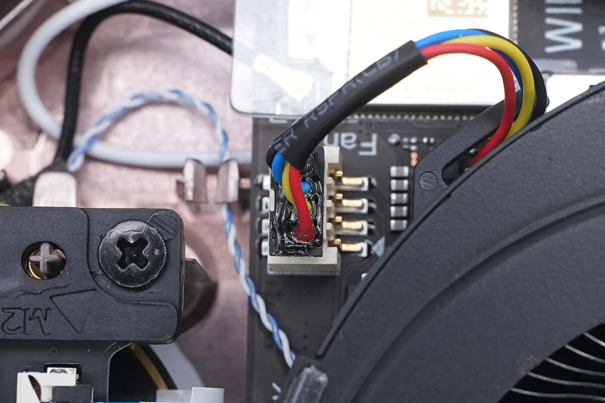
Close-up of the cooling fan connector.
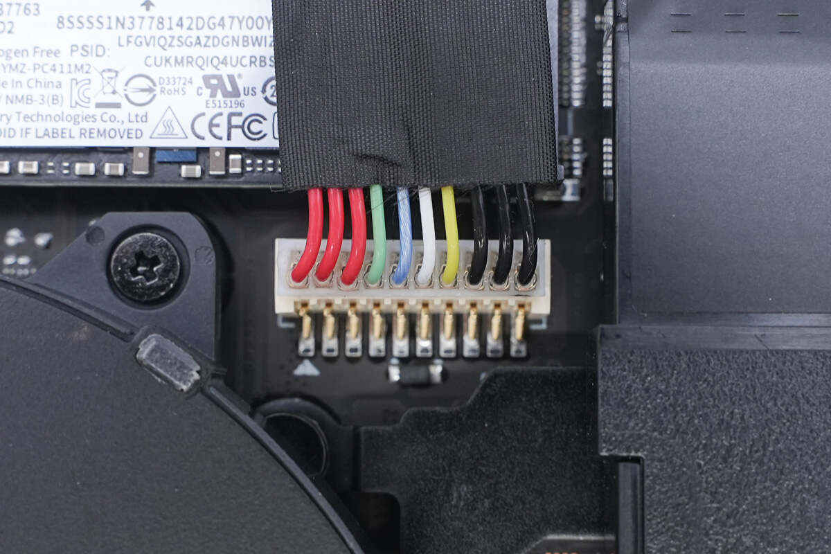
Close-up of the battery pack connector.
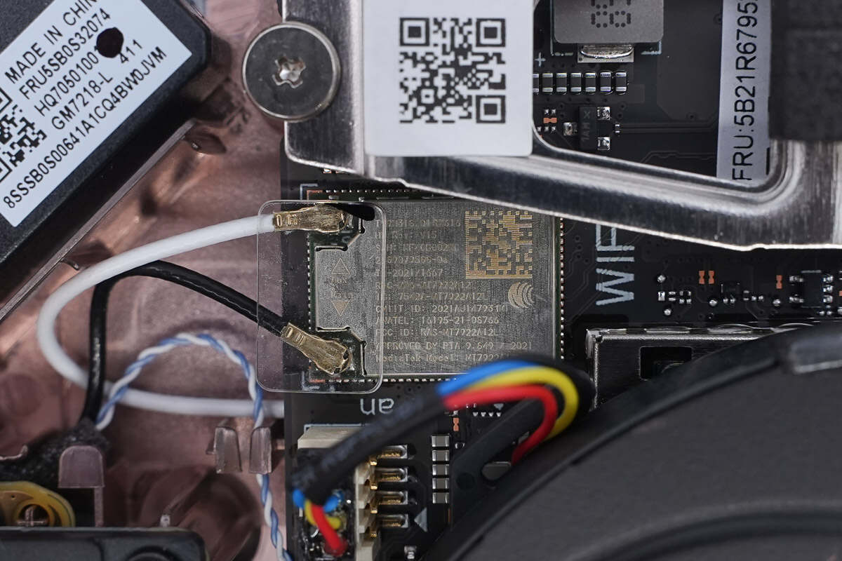
The WiFi antenna is connected via a connector.
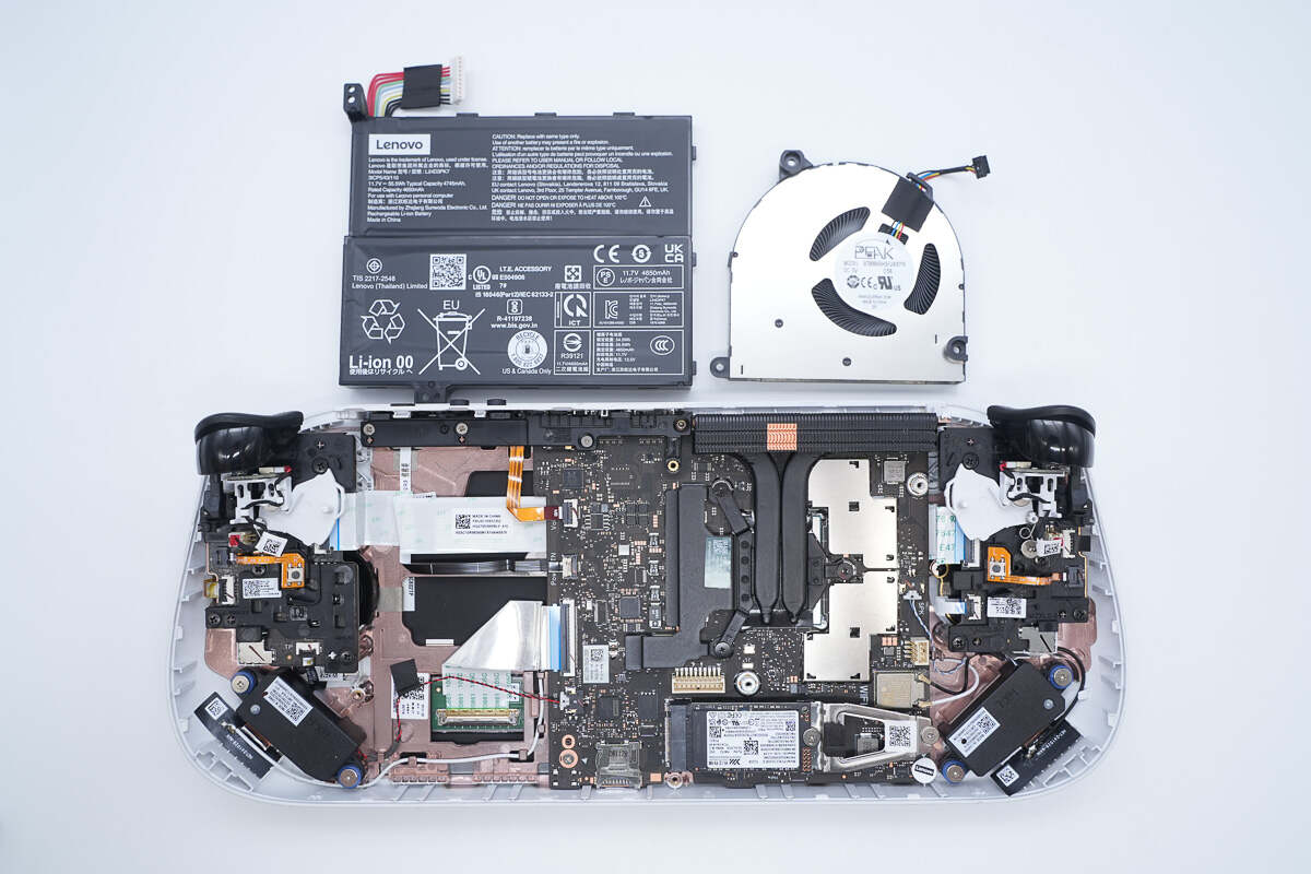
Unscrew the screws to remove the battery pack and cooling fan.
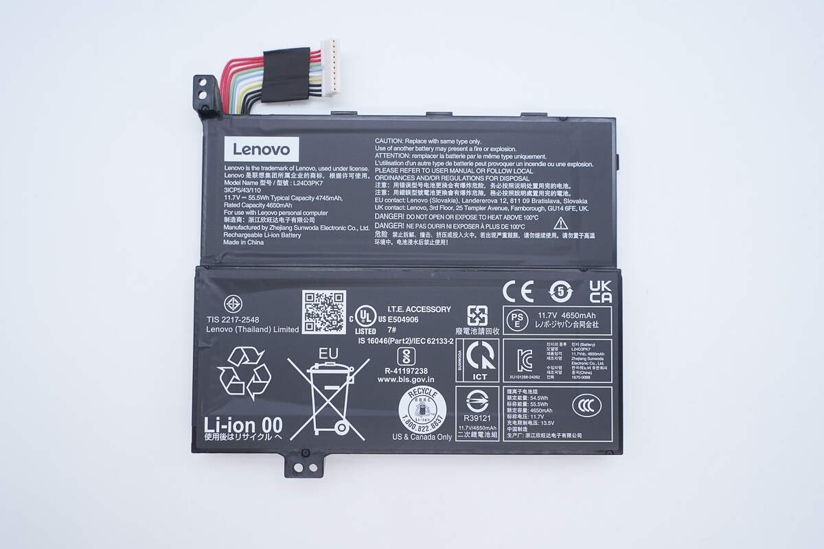
The battery pack is enclosed in a plastic casing and secured with screws.
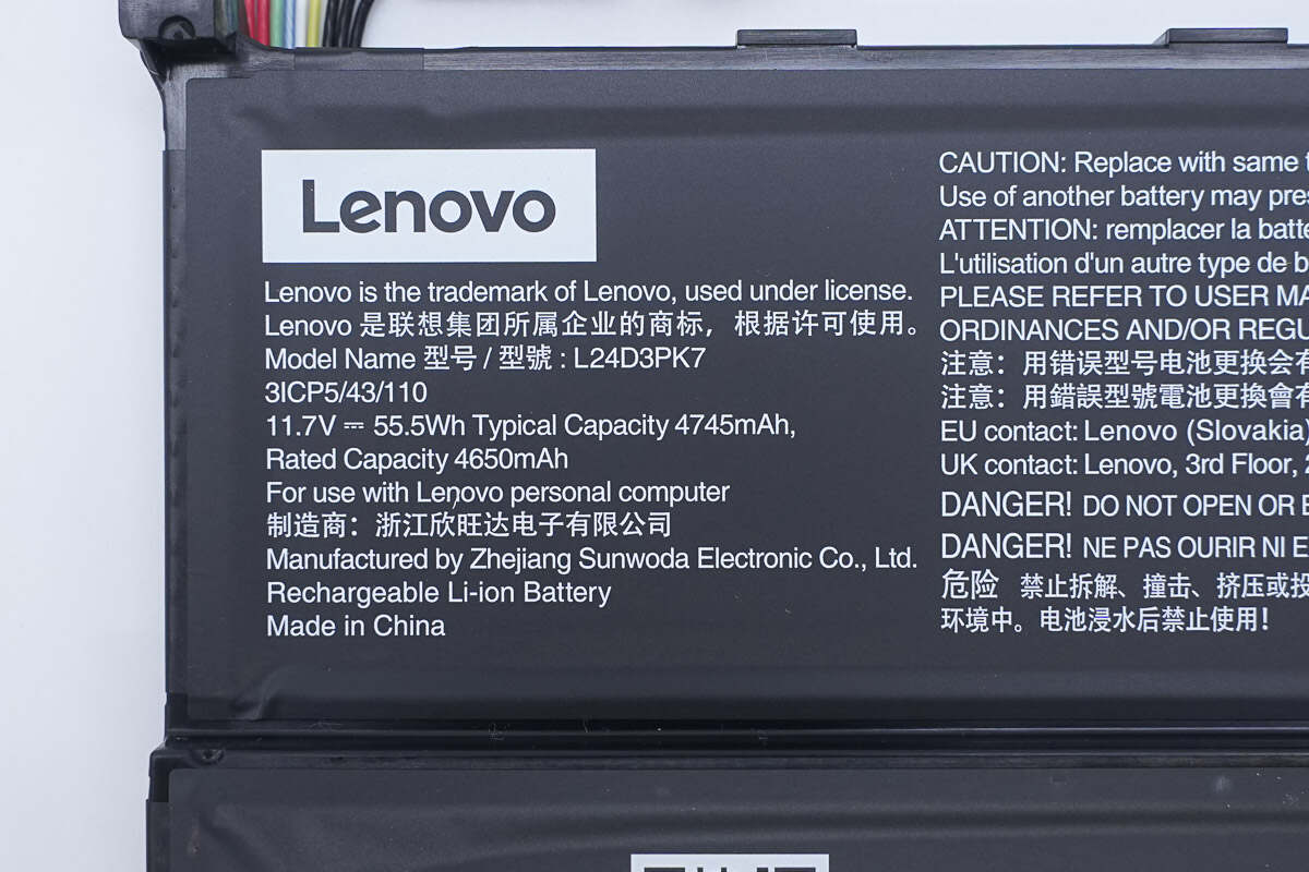
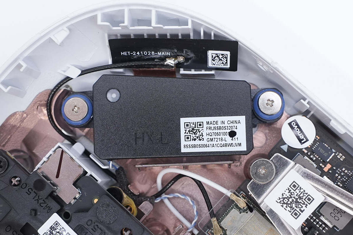
The battery pack model is L24D3PK7, with a nominal voltage of 11.7V and an energy capacity of 55.5Wh. It has a typical capacity of 4745mAh and a rated capacity of 4650mAh. The battery is manufactured by Zhejiang Sunwoda Electronics Co., Ltd.
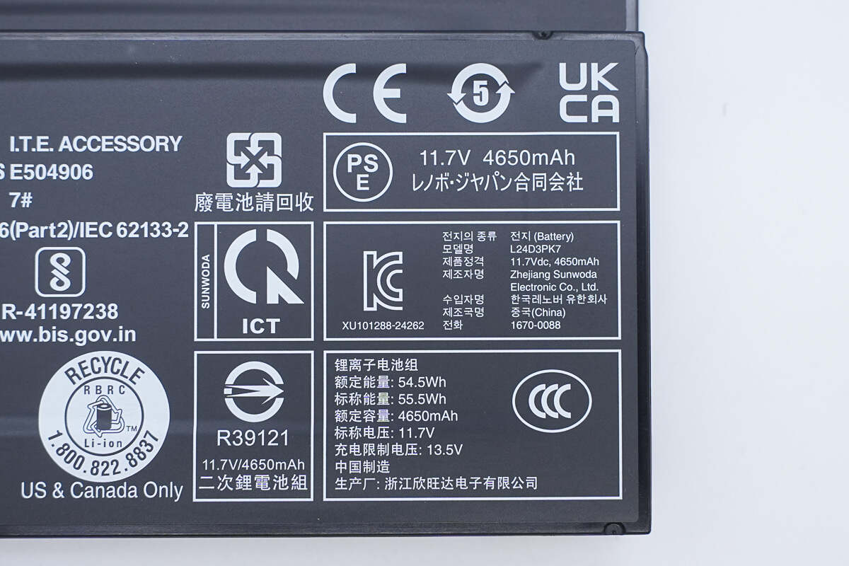
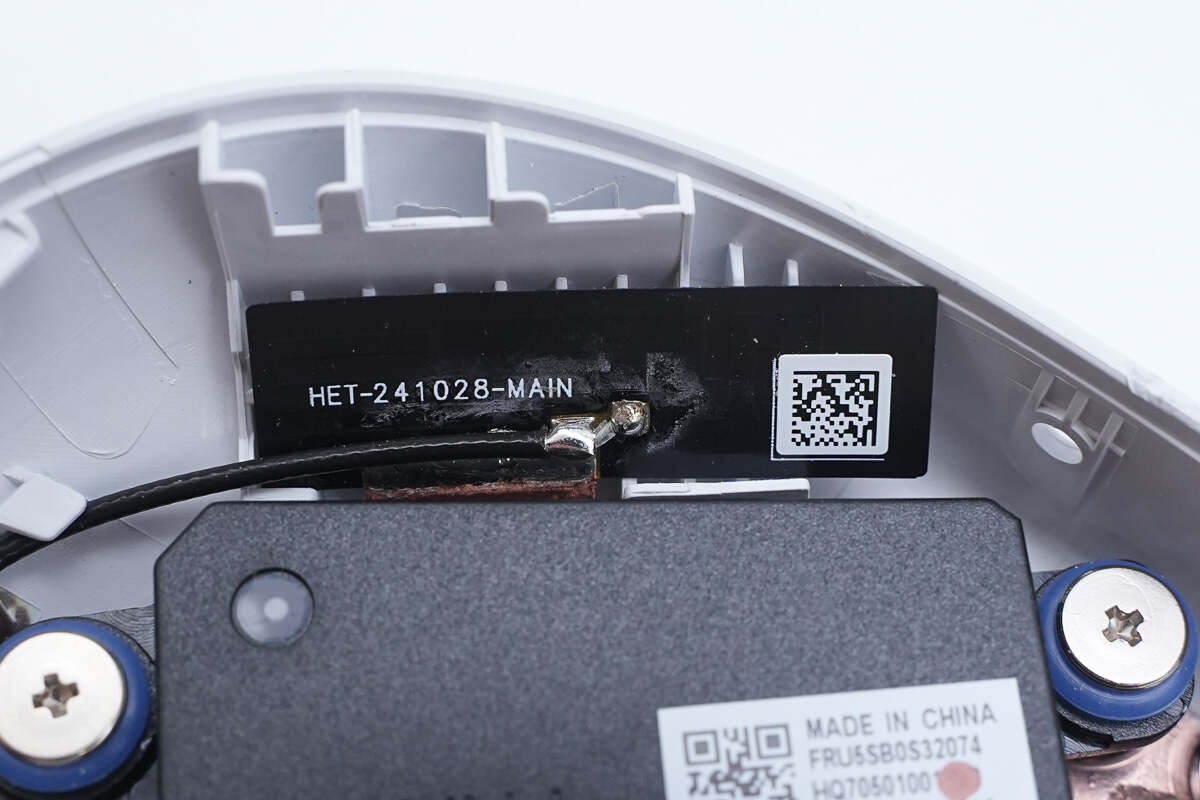
Battery information is labeled on the bottom right corner.
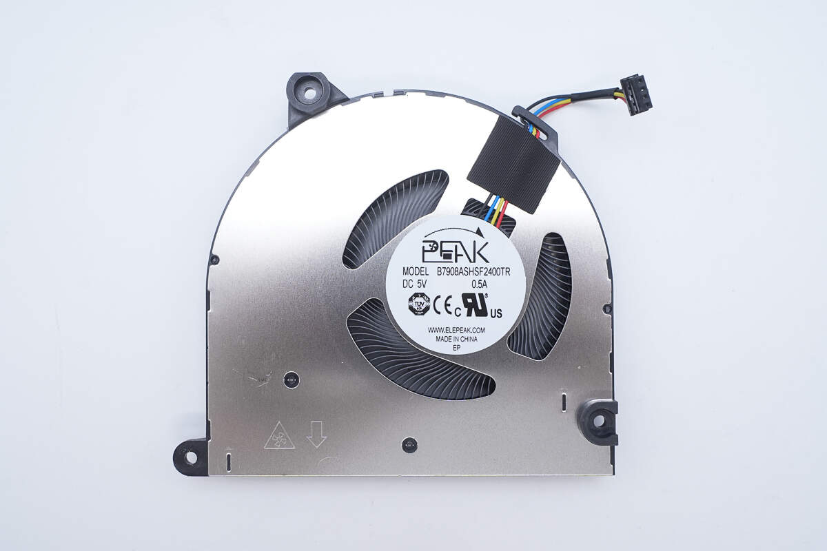
Close-up of the centrifugal cooling fan.
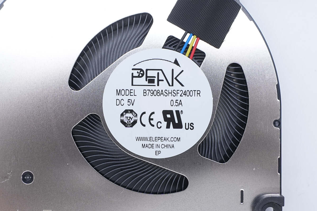
The cooling fan is manufactured by Kunshan Pindai Electrical Co., Ltd. It is a four-wire PWM fan, with a sticker indicating the clockwise rotation direction. 5V 0.5A. Model is B7908ASHSF2400TR.
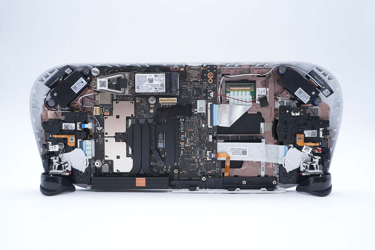
After removing the cooling fan and battery pack, the internal layout is fully exposed. The mainboard is connected to the display and the right-side daughterboard via ribbon cables.
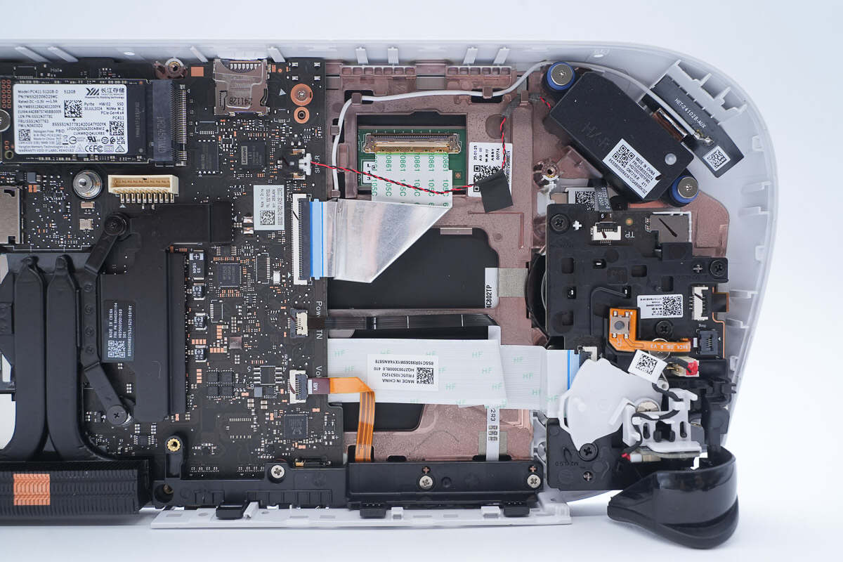
Aluminum foil is applied to the display ribbon cable for shielding.
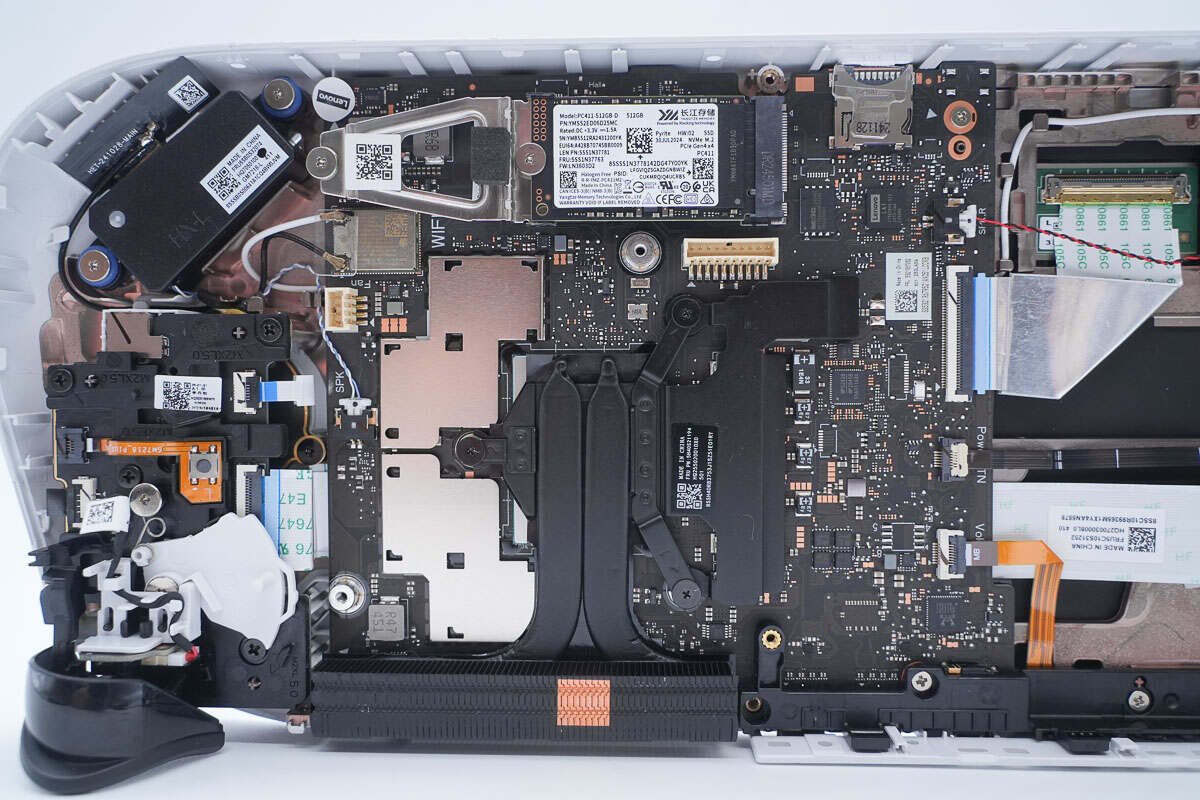
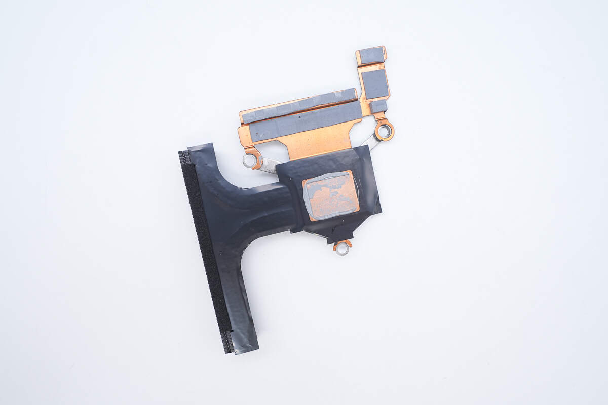
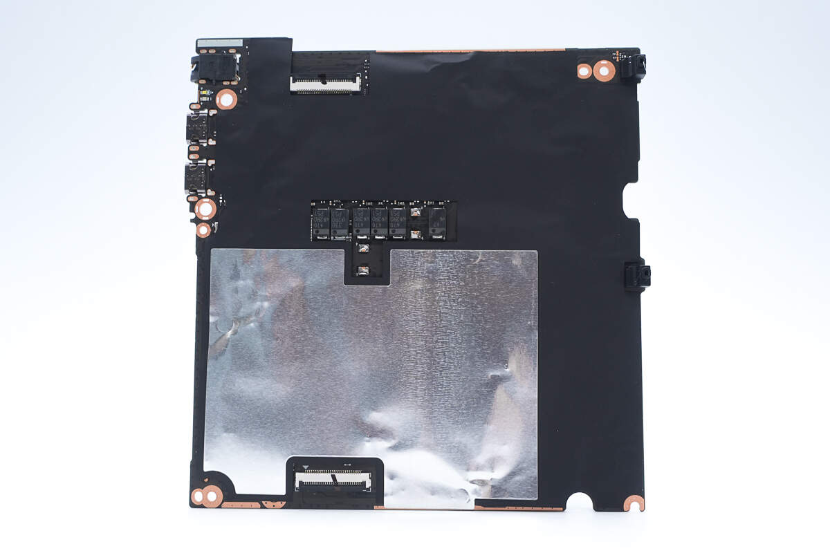
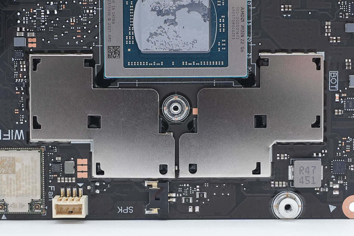
The mainboard is equipped with a shielding cover, and the heat pipe cooler is secured with screws.
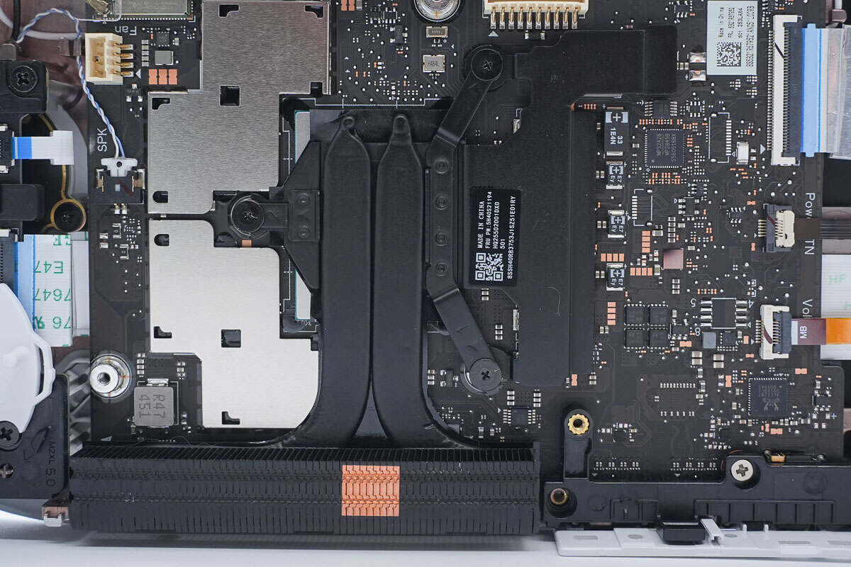
The two heat pipe coolers are secured with three screws and also provides cooling for the power delivery circuitry.
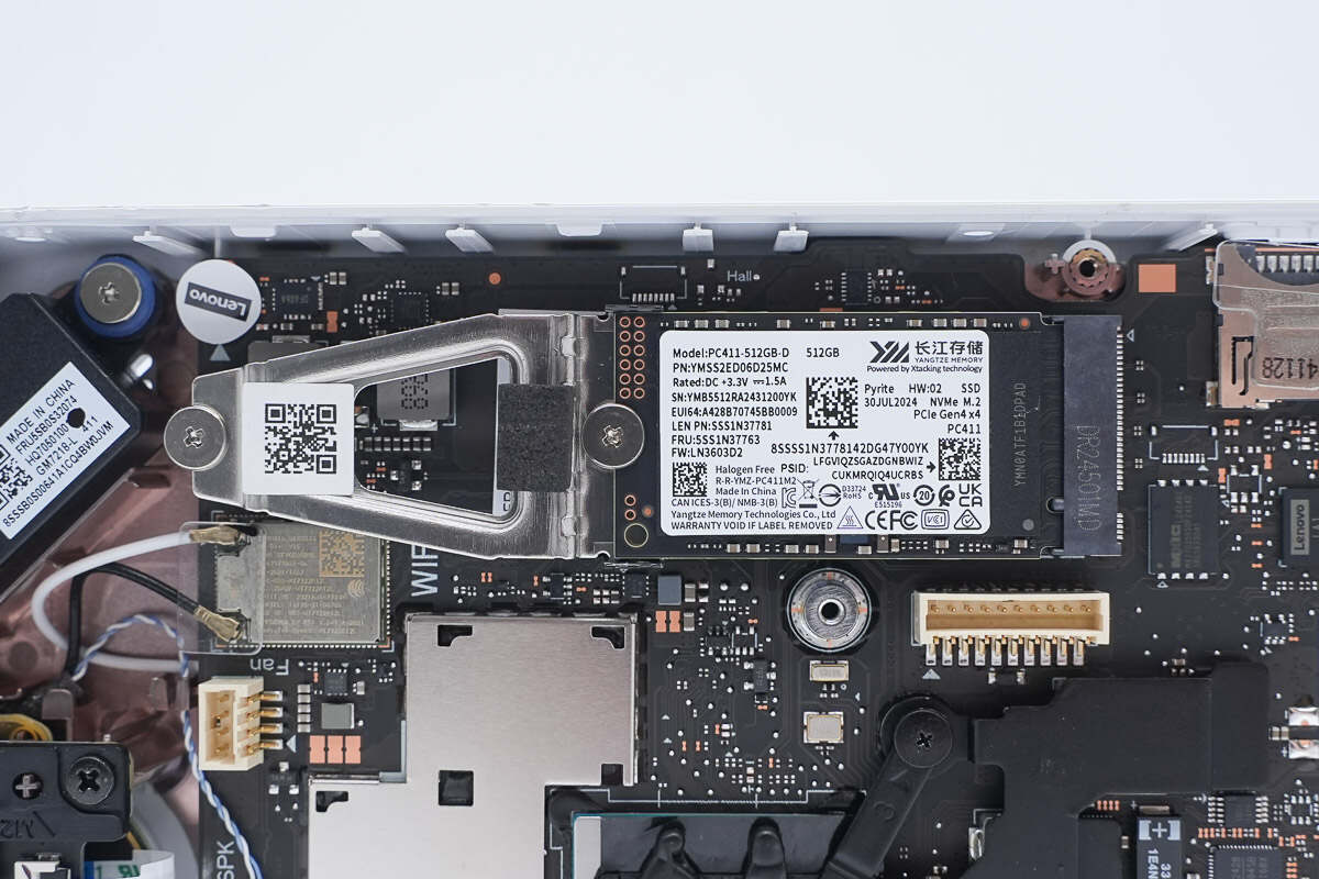
The SSD is from Yangtze Memory Technologies, with a capacity of 512 GB. It uses a PCIe Gen4 x4 interface and has a 2242 form factor. Model is PC411-512GB-D.
Close-up of the connector for the right-side speaker.
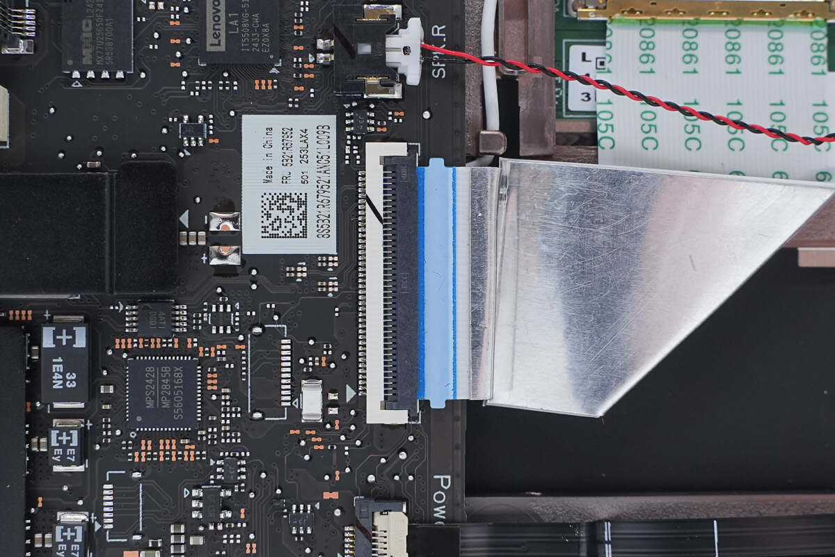
Close-up of the display ribbon cable.
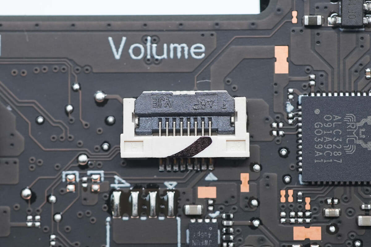
Close-up of the ribbon cable for the volume buttons.
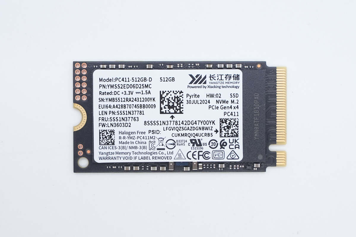
The Yangtze Memory PC411 SSD features a PCIe Gen4 x4 interface and NVMe 1.4 protocol. It is compatible with mainstream computer motherboards and comes in a single-sided design supporting both 2242 and 2280 form factors. This enhanced physical compatibility makes it ideal for devices with limited space slots, such as laptops and PlayStation gaming consoles.
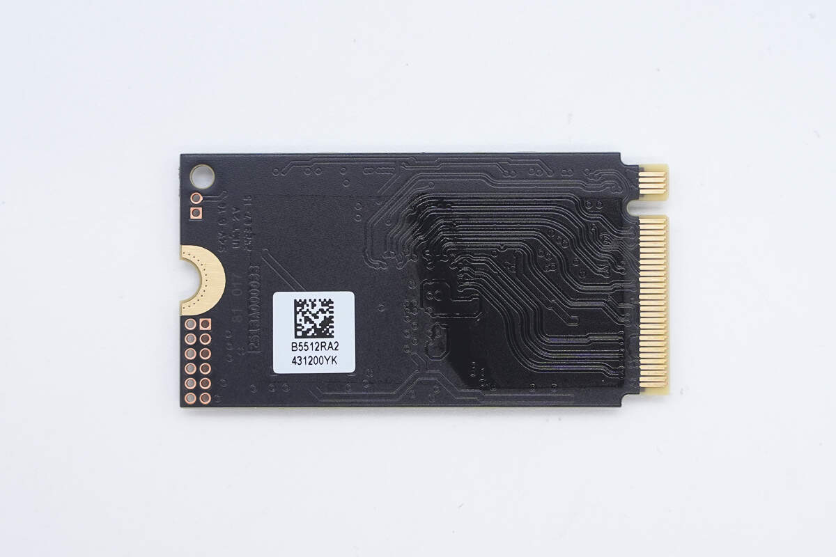
The SSD features a single-sided design.
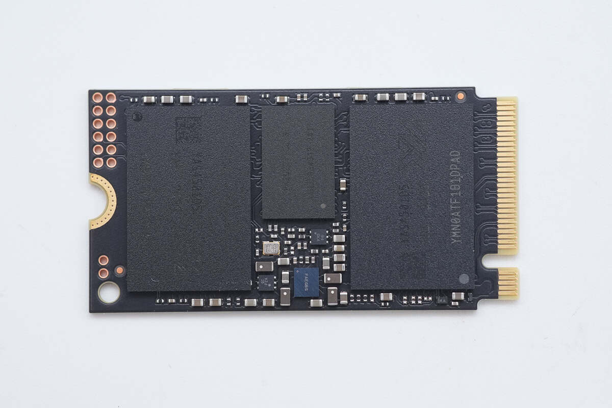
Peel off the label on the front of the SSD. The master controller chip is located in the center, flash memory chips are positioned on both sides, and the PMIC is situated at the bottom.
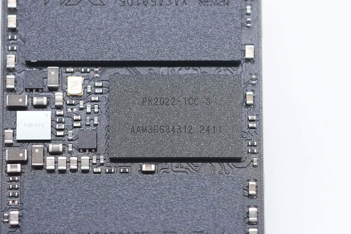
The master controller chip is marked with PK2022-10C S.
Close-up of the external clock chip for the main controller.
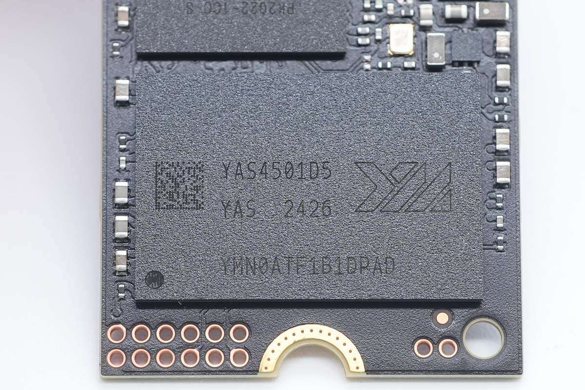
Flash memory chips, each with a capacity of 256 GB. Model is YMN0ATF1B1DPAD
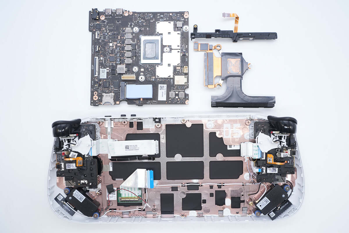
Disconnect the ribbon cables, remove the heatsink, and take out the motherboard from the case.
An insulating sheet is placed on the motherboard beneath the cooling assembly, with thermal pads applied over the power ICs and power inductors.
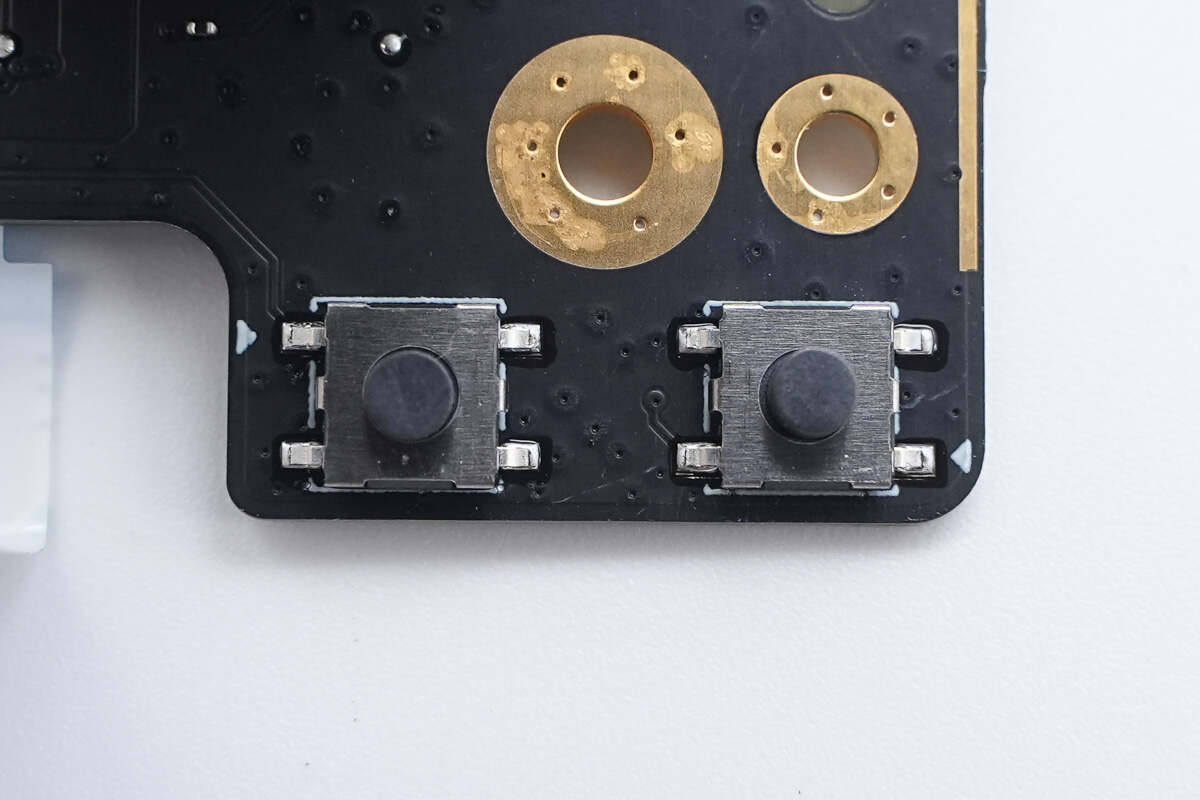
The pressure plate is equipped with volume buttons.
Close-up of the volume button dome switch.
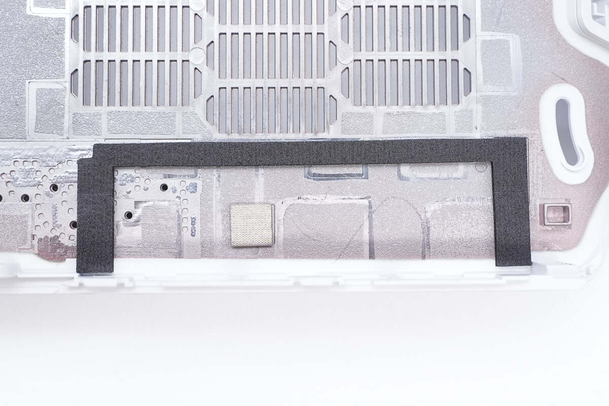
The interior of the case features a hollowed-out design.
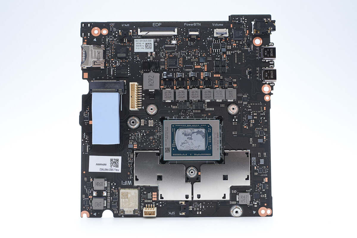
On the front side of the mainboard is the CPU. Below the CPU are two shielding covers housing the memory chips. Above the CPU are the power delivery components, including DrMOS, power inductors, and a power controller. In the upper-left corner are the embedded controller (EC) chip and its associated memory. Below these lies the SSD slot, and in the lower-left corner is the wireless network card. The upper-right corner houses the audio codec chip, the 3.5mm audio jack, and two USB-C ports.
The back of the mainboard is covered with a black plastic insulating film, with aluminum foil shielding applied at the area corresponding to the back of the CPU.
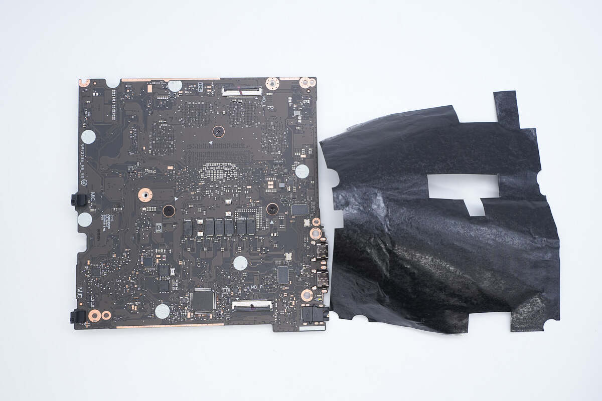
Peel off the black plastic insulating film.
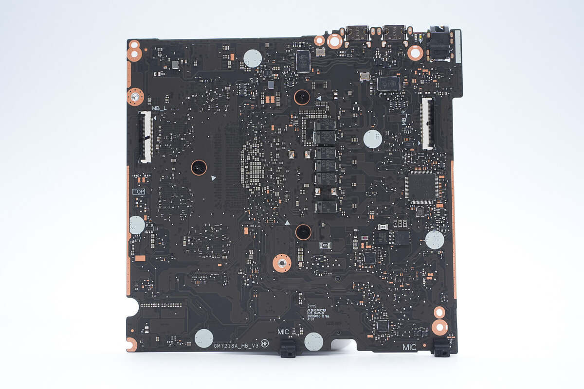
On the back of the mainboard are CPU power filtering capacitors, the retimer chip for the USB-C ports, the MCU, the battery charging chip, and the card reader chip.
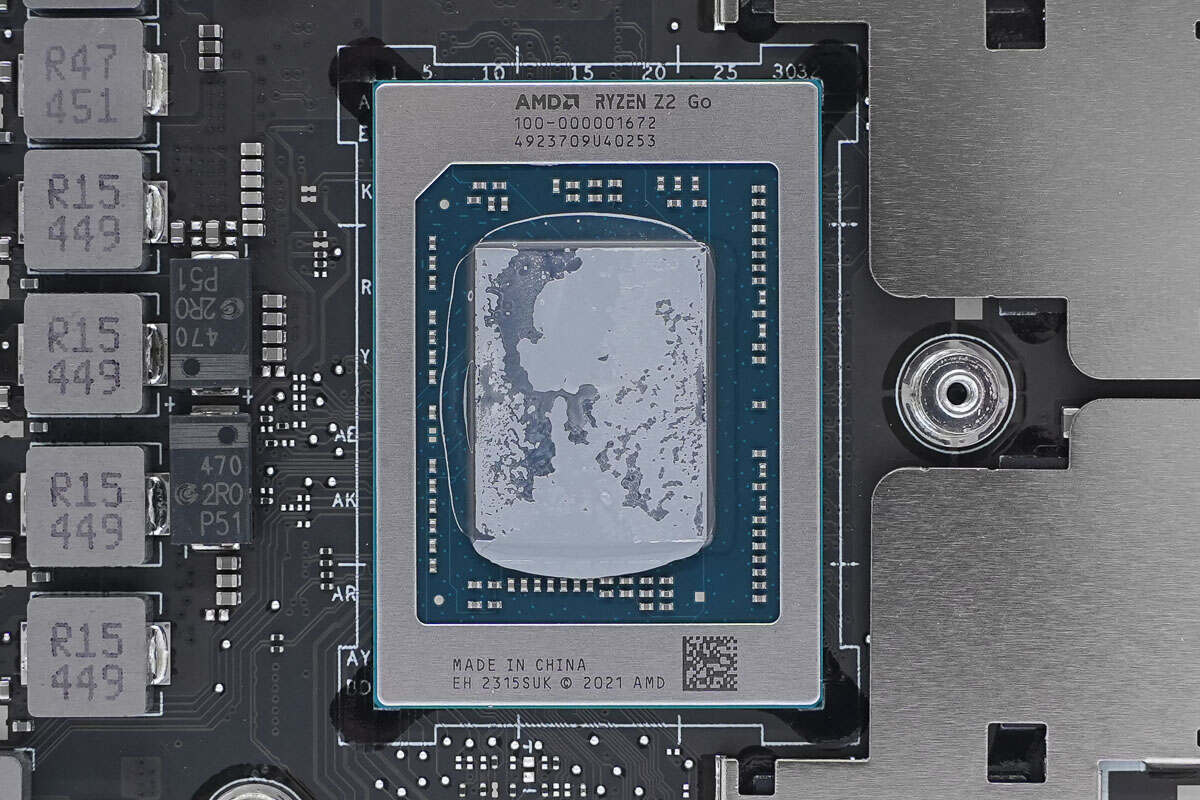
The AMD RYZEN Z2 Go processor is based on the Zen 3+ architecture, featuring 4 cores and 8 threads with a maximum boost clock of 4.3 GHz. It integrates 12 RDNA 2 GPU cores.
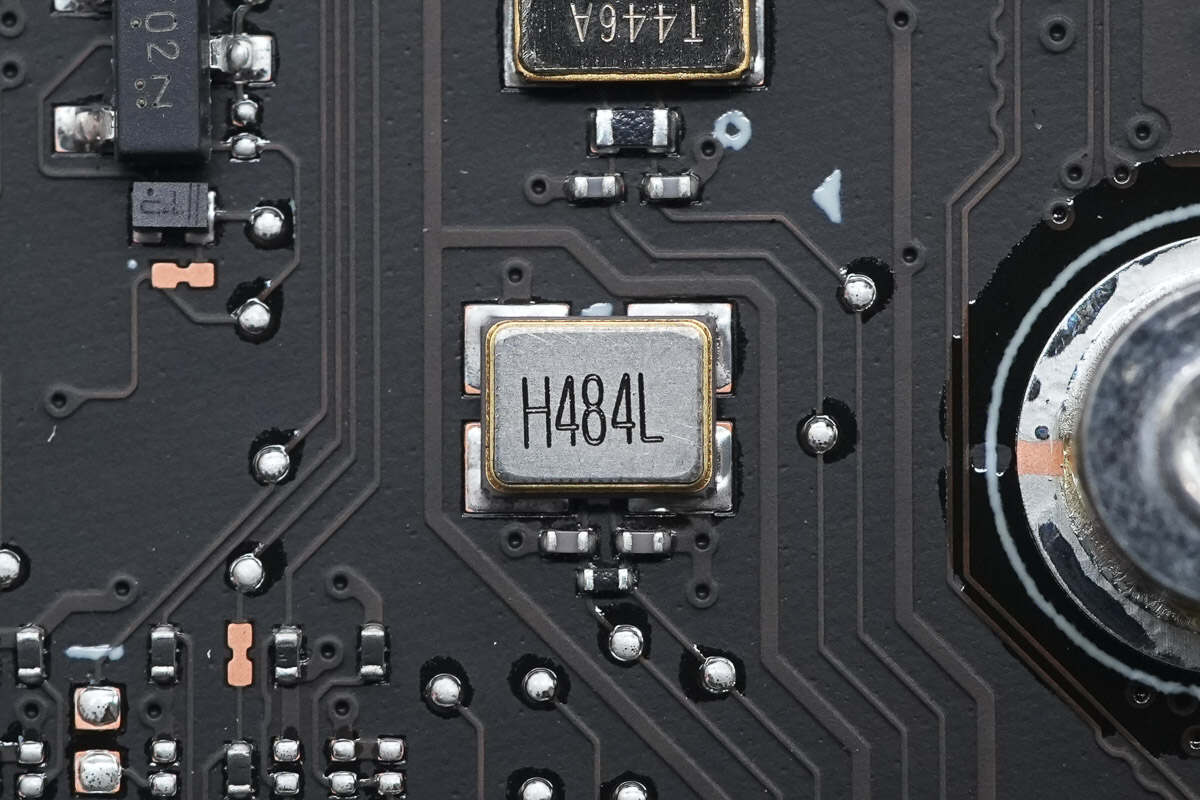
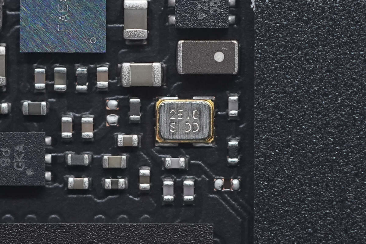
Close-up of the 48.000 MHz crystal oscillator.
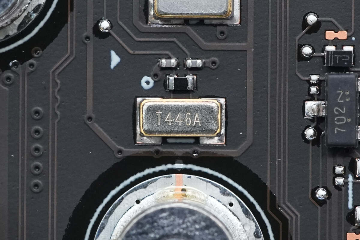
Close-up of the 32.768 KHz crystal oscillator.
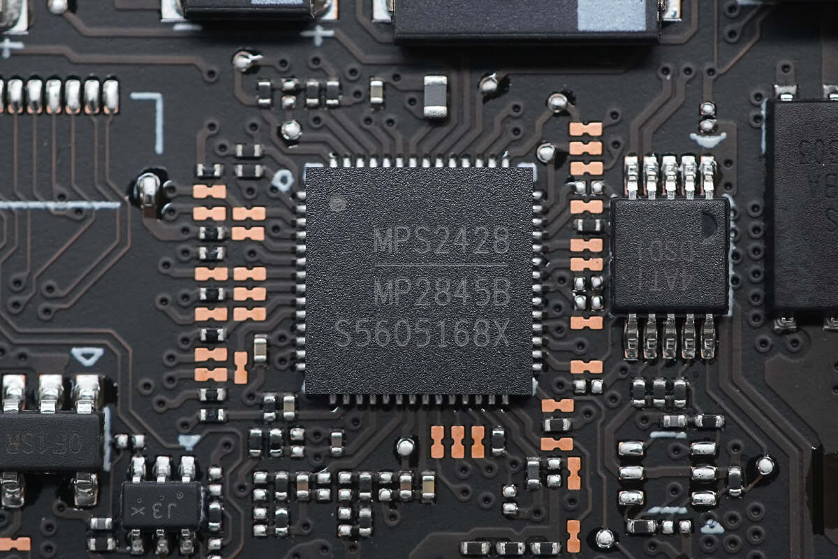
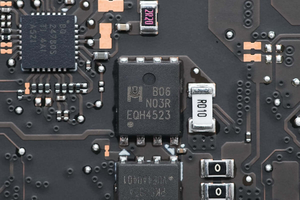
The power delivery controller is from MPS. Model is MP2845B。
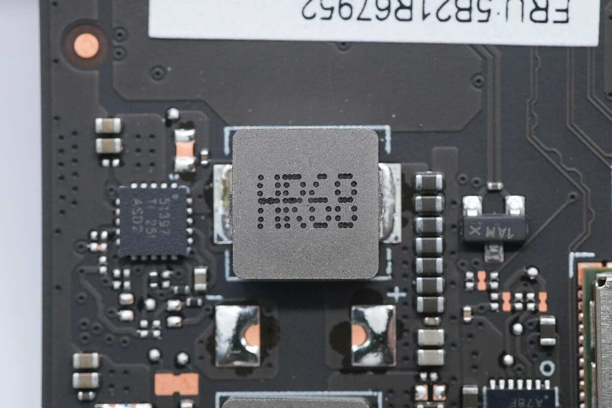
Close-up of the four-phase DrMOS used for CPU core power delivery.
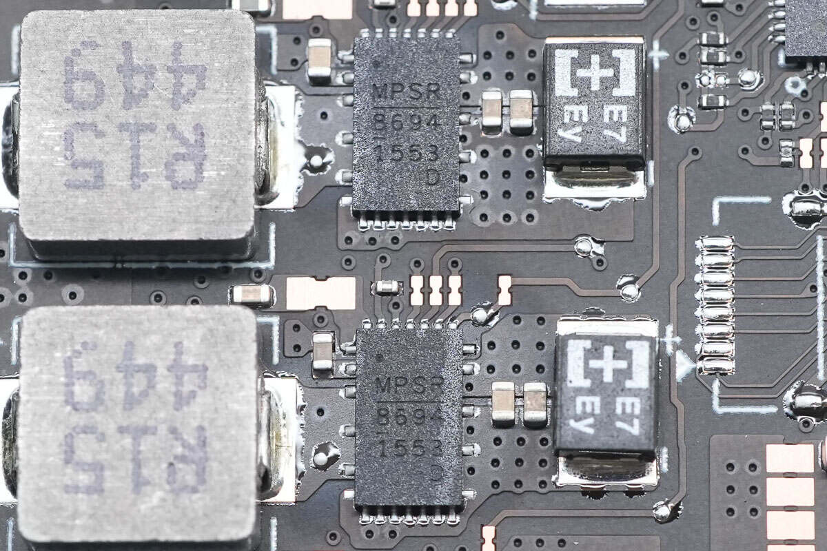
The DrMOS is from MPS. Model is MP86941.
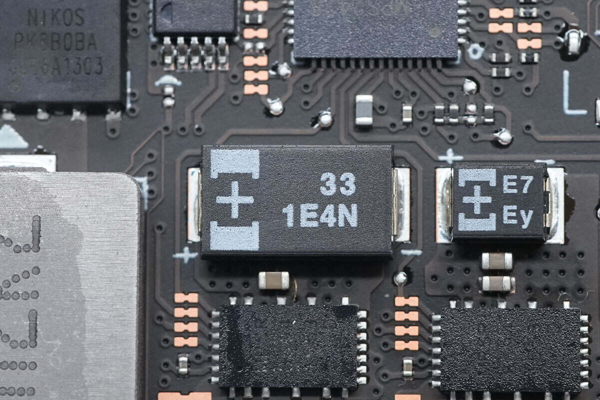
The power filtering capacitors are from Panasonic. 33μF 25V.
These power filtering capacitors are rated at 15μF and 25V.
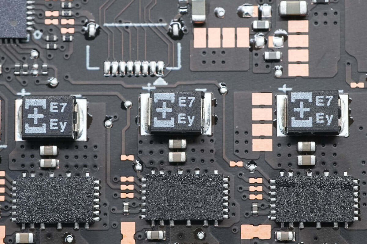
The capacitors for output filtering are from APAQ. 470μF 2V.
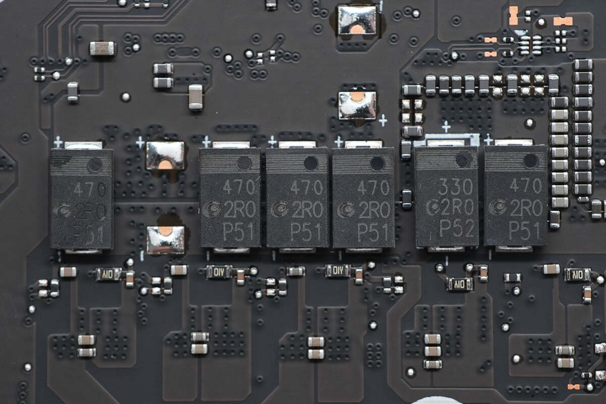
On the back, there are six filter capacitors, five of which are rated at 470μF and 2V.
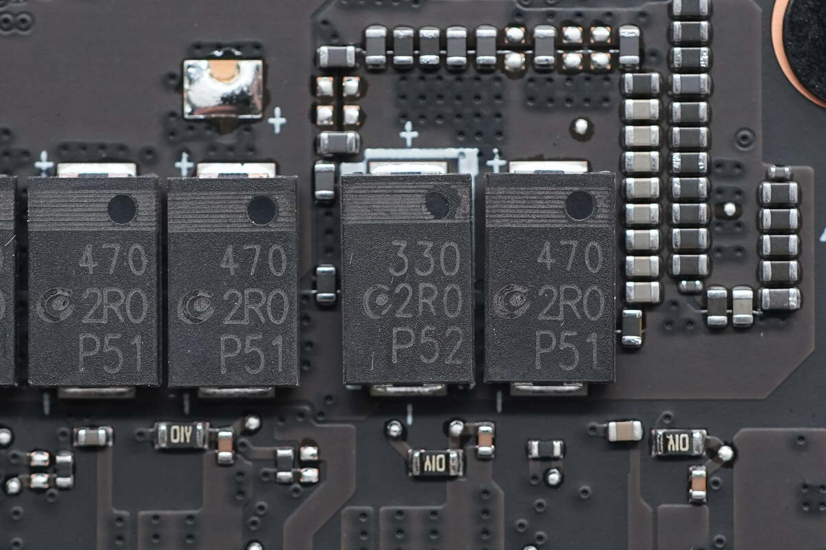
The remaining one is rated at 330μF and 2V.
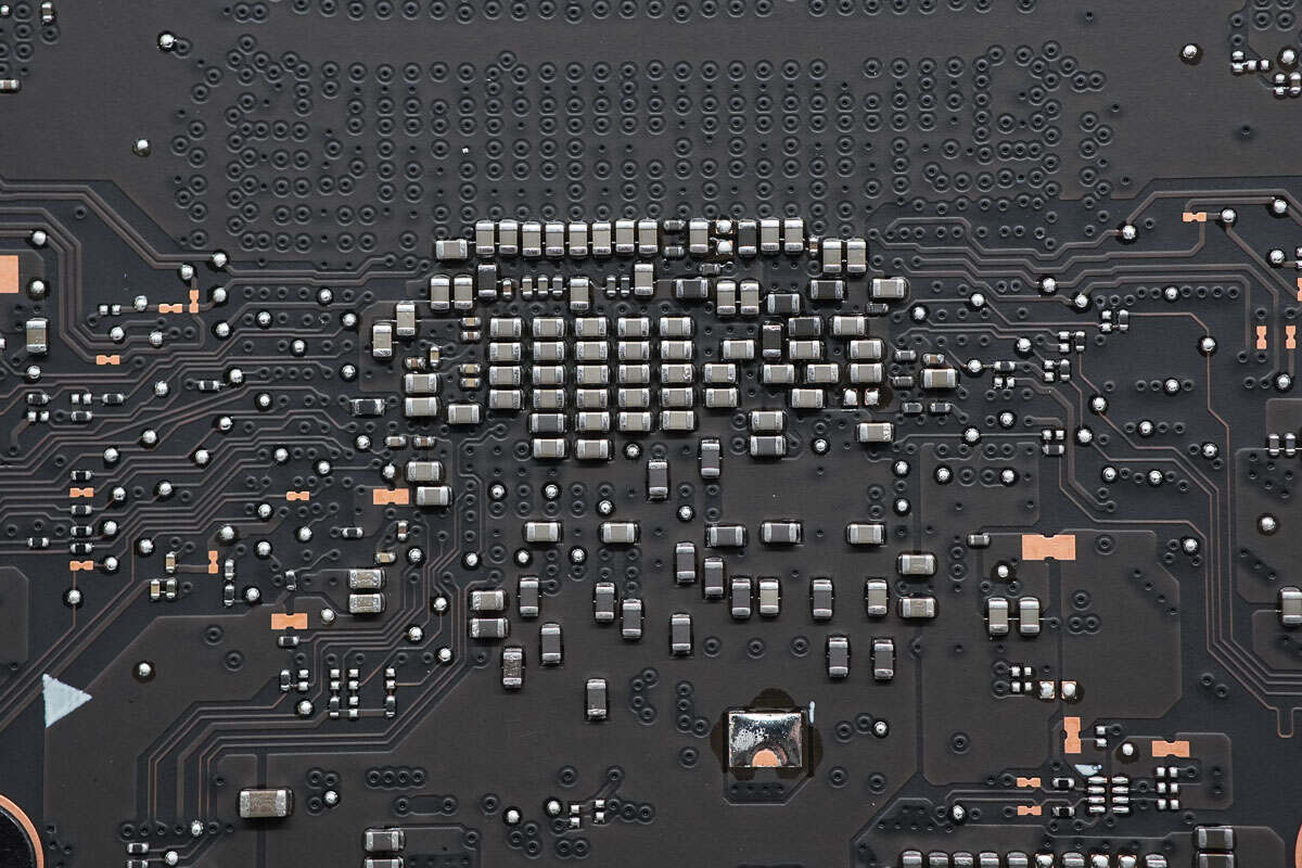
The back of the CPU features MLCC capacitors.
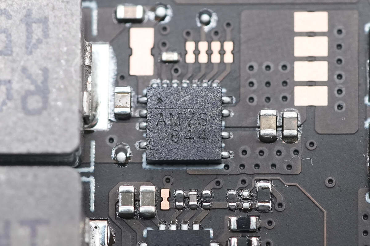
The DrMOS marked with AMV is from MPS and adopts a QFN-13 package. Model is MP86901-AGQT.
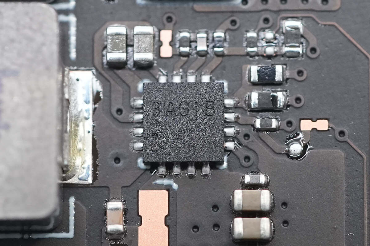
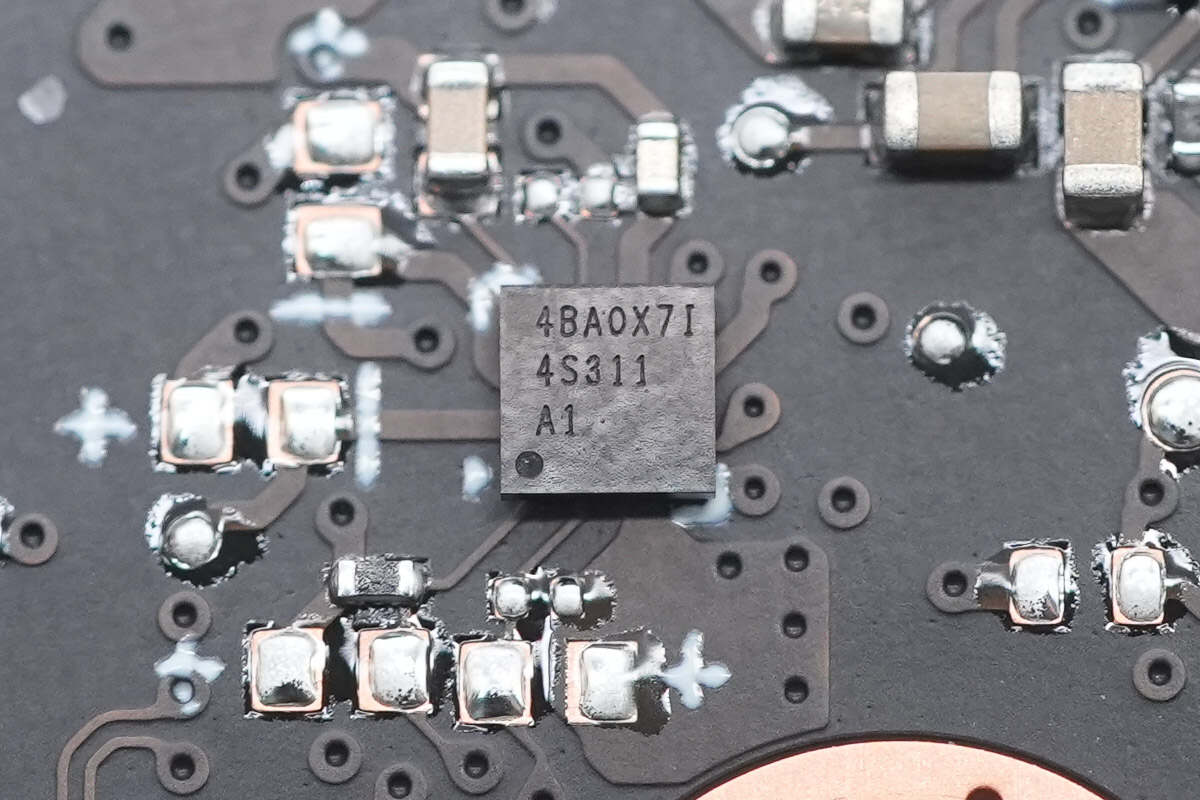
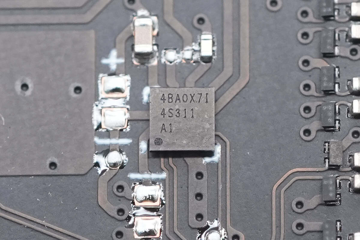
This chip is marked with 3AGjB.
Below the CPU, there are two shielding covers housing the memory chips.
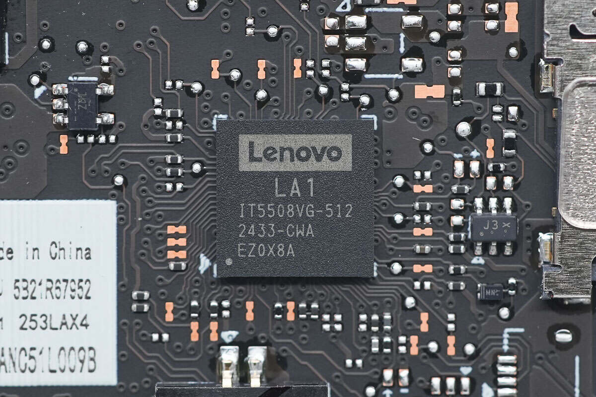
The IO chip is marked with the Lenovo logo and LA1 IT5508VG-512.
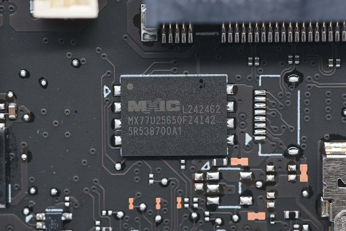
The memory chip is from MXIC, with a capacity of 32MB, packaged in a WSON-8 form factor. Model is MX77U25650FZ4I42.
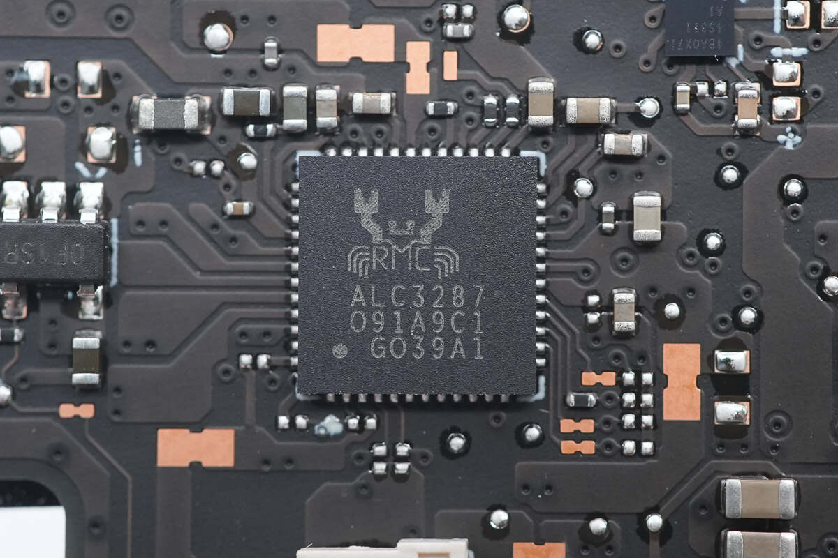
The audio chip is from REALTEK and uses a QFN48 package. Model is ALC3287.
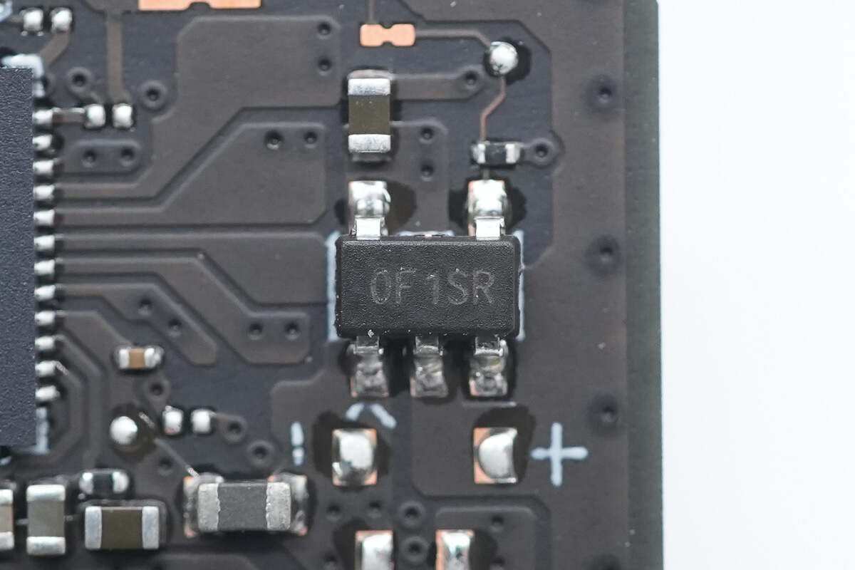
This chip is marked with 0F1SR.
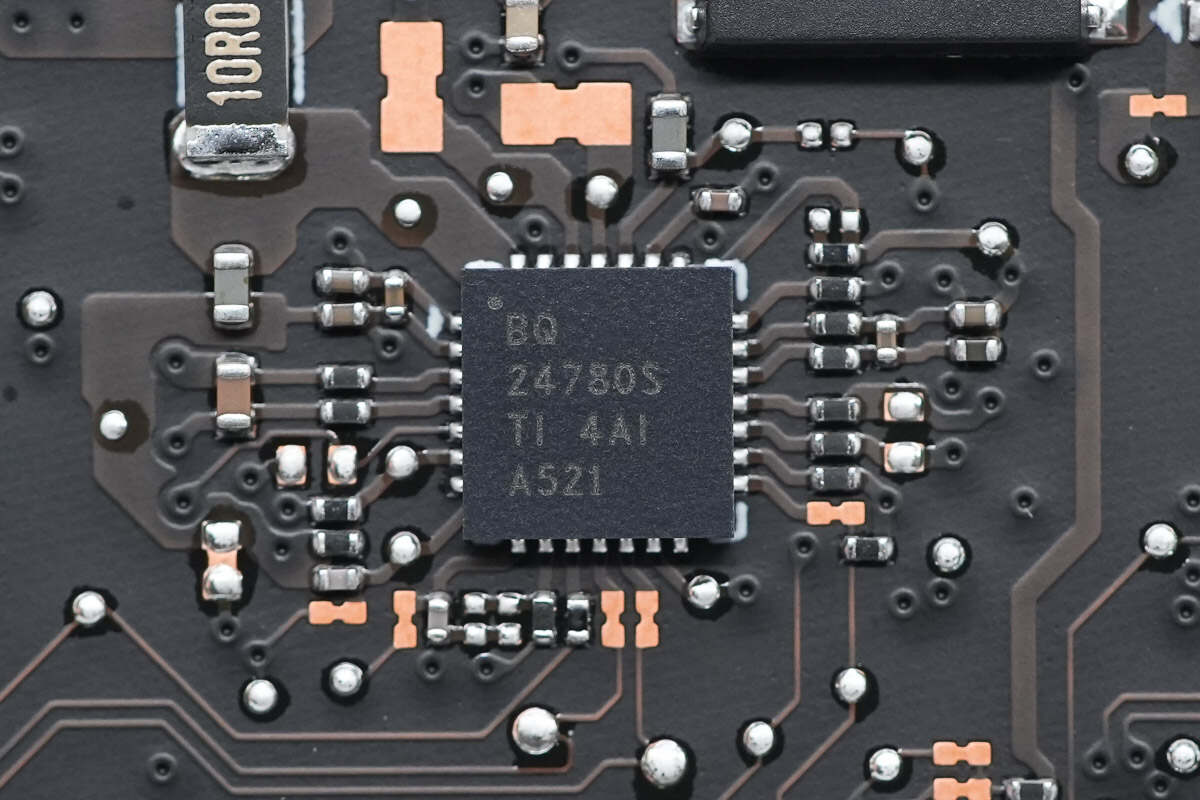
The battery charging chip is from TI. It is a charging controller supporting hybrid boost mode, compatible with input voltages from 4.5V to 24V, and designed for 1 to 4 cell battery applications. The chip features synchronous buck charging and supports hybrid boost mode. It comes in a WQFN28 package. Model is BQ24780S.
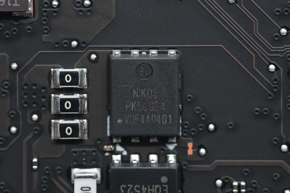
The VBUS MOSFET is from NIKO-SEM. It is an NMOS with a voltage rating of 30V and an on-resistance of 2.4mΩ, housed in a PDFN 5x6P package. Model is PK5C8EA.
The VBUS MOSFET is from Excelliance. It is an NMOS with a voltage rating of 30V and an on-resistance of 6mΩ, packaged in an EDFN 5x6 form factor. Model is EMB06N03HR.
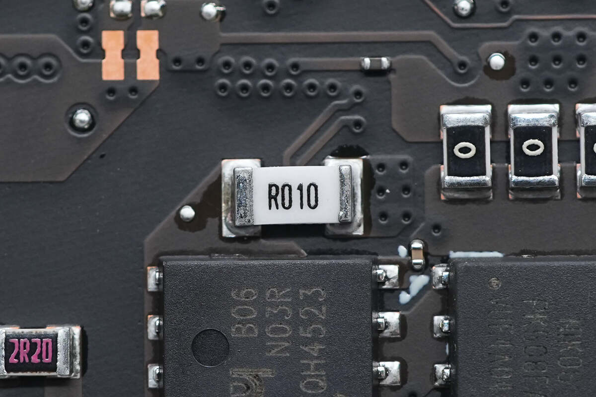
The current sensing resistor is used for input current detection. 10mΩ.
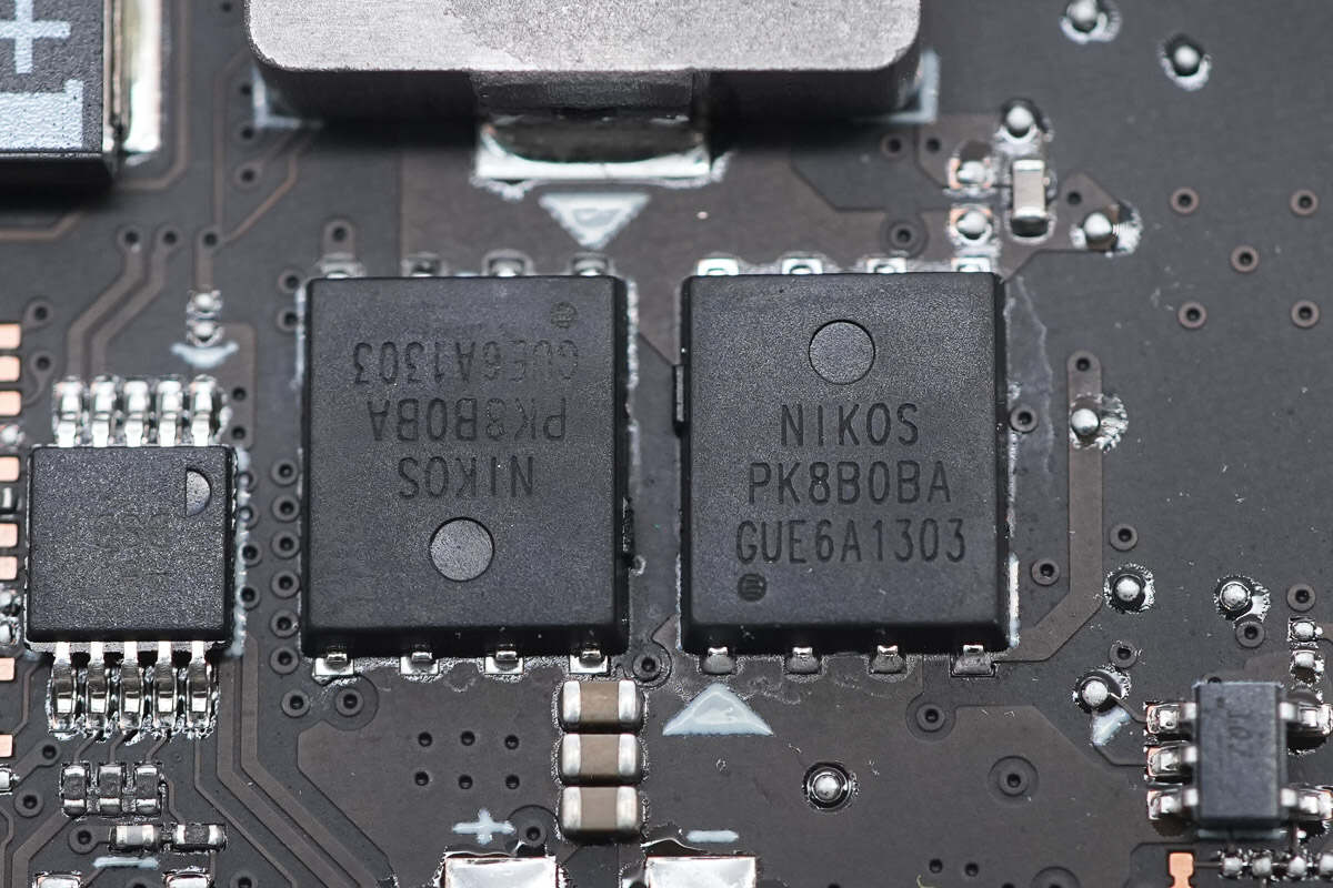
The two MOSFETs used for charging are from NIKO-SEM. They are NMOS with a voltage rating of 30V and an on-resistance of 7.8mΩ, packaged in a PDFN 5x6P form factor. Model is PK8B0BA.
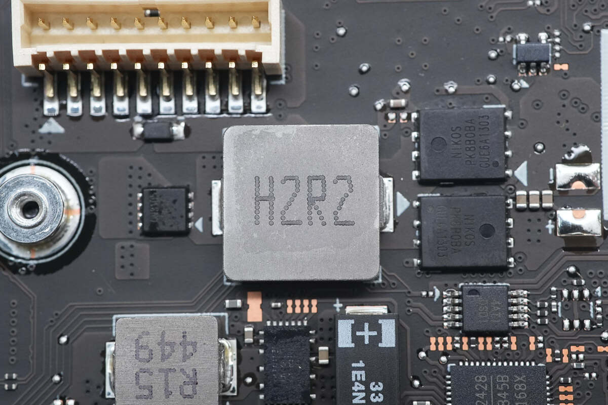
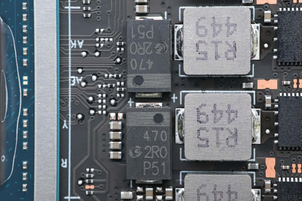
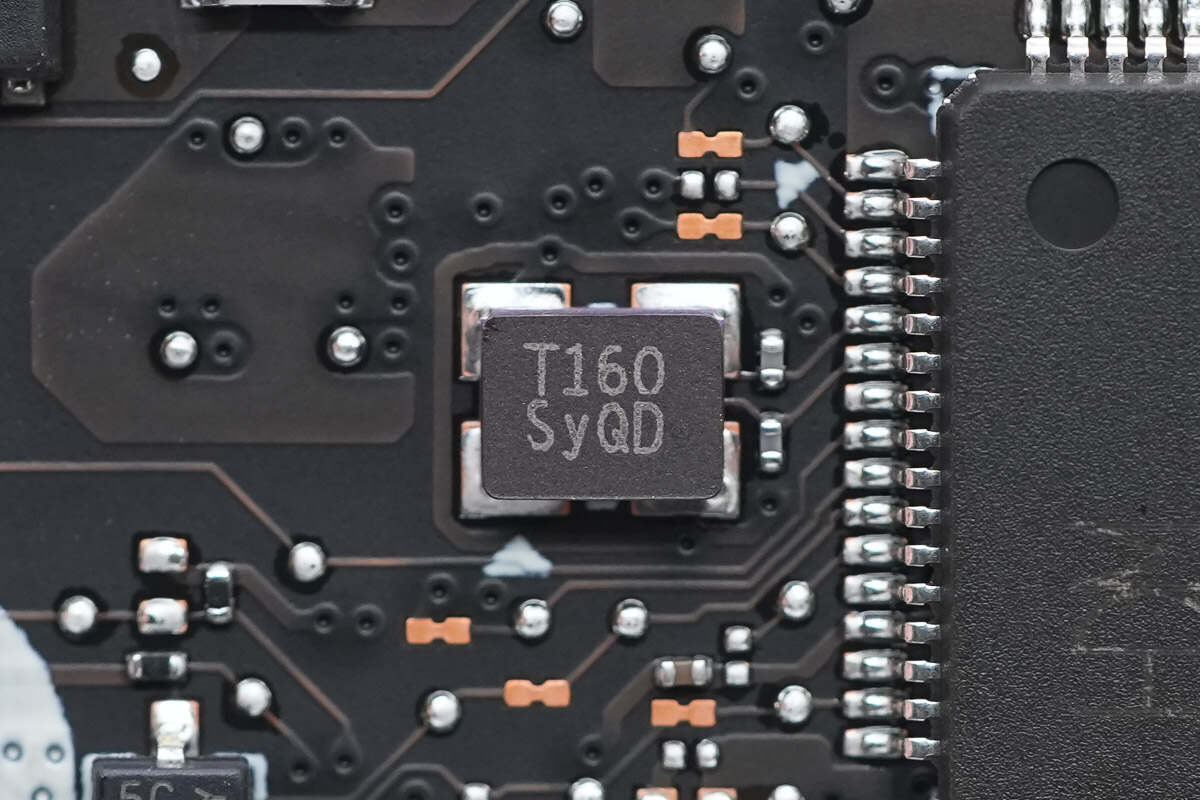
Close-up of the 2.2μH alloy inductor.
The 5mΩ sense resistor is used for battery-side current detection.
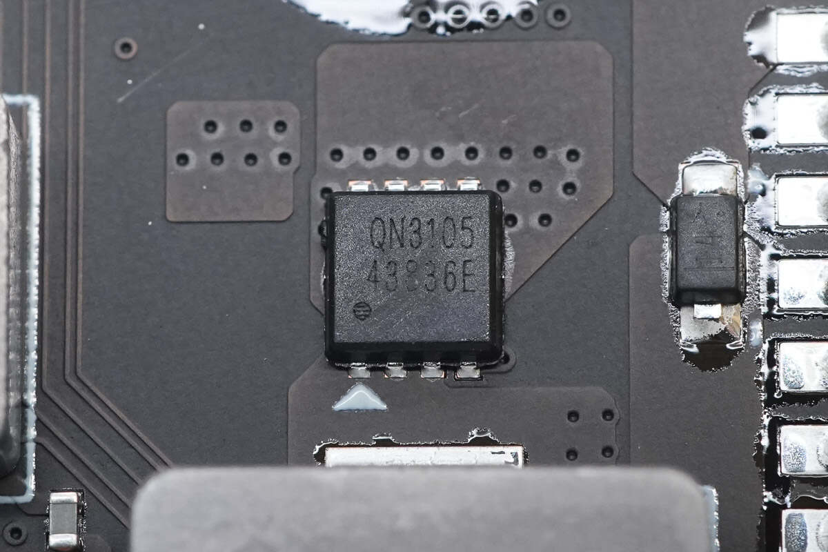
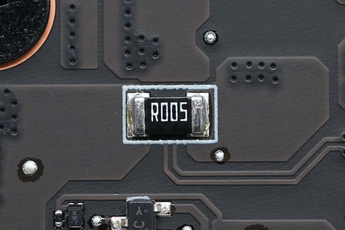
The battery-side MOSFET is from uPI SEMI. It is an NMOS with a voltage rating of 30V and an on-resistance of 4.5mΩ, packaged in a PRPAK 3x3 form factor. Model is QN3105M3N.
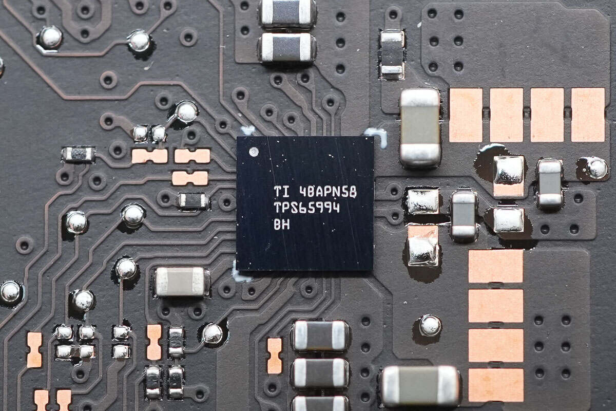
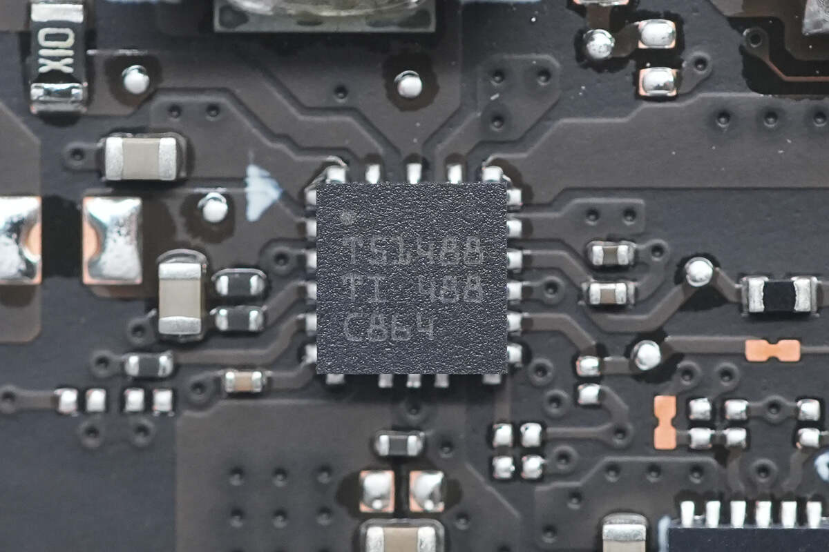
The USB-C controller is from TI. It is used for dual USB-C port control and supports PC and laptop applications. Model is TPS65994BH.
The VBUS MOSFET is from Excelliance. It is an NMOS with a voltage rating of 30V and an on-resistance of 7mΩ, packaged in an EDFN 3x3 form factor. Model is EMB07N03V.
The USB-C protector is from TI. It features overvoltage protection for CC1, CC2, SBU1, and SBU2 pins, with 35V surge protection on the CC pins and 30V surge protection on the SBU pins. It also supports 600mA Vconn power supply and comes in a DSBGA16 package. Model is TPD4S311A.
The other protector is of the same model, protecting each of the two USB-C ports.
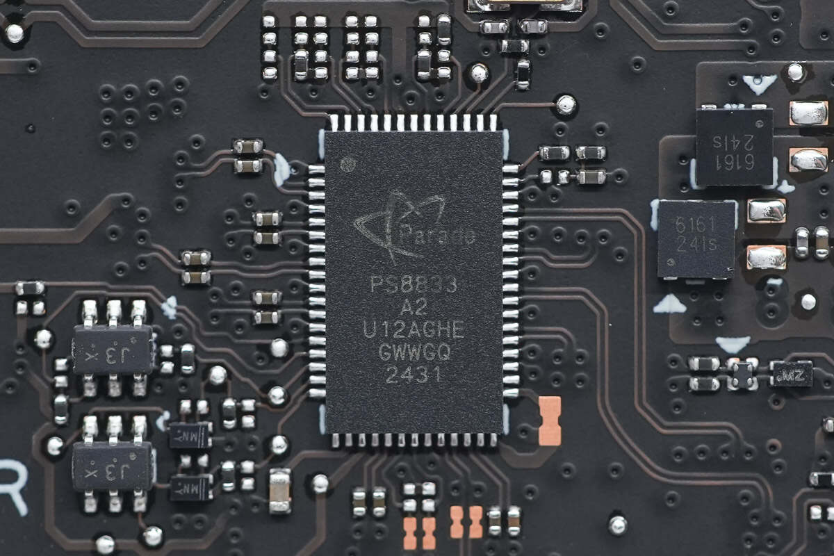
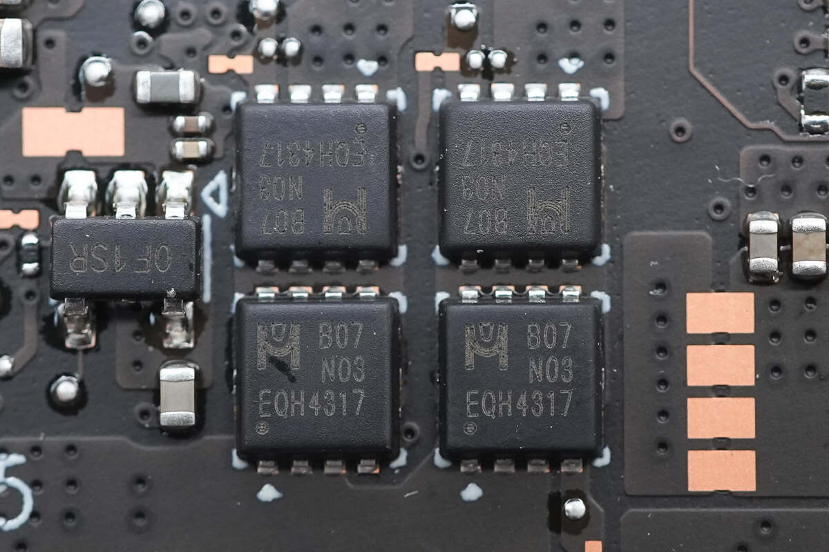
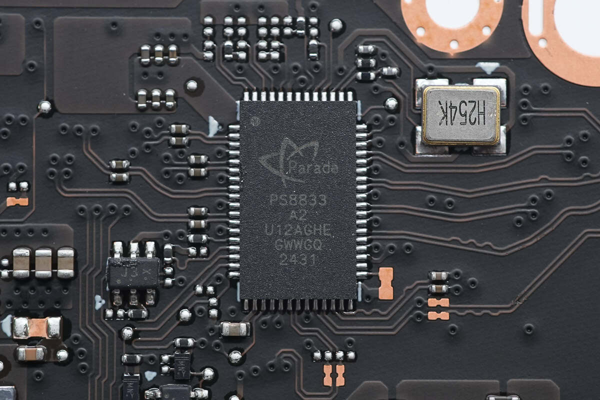
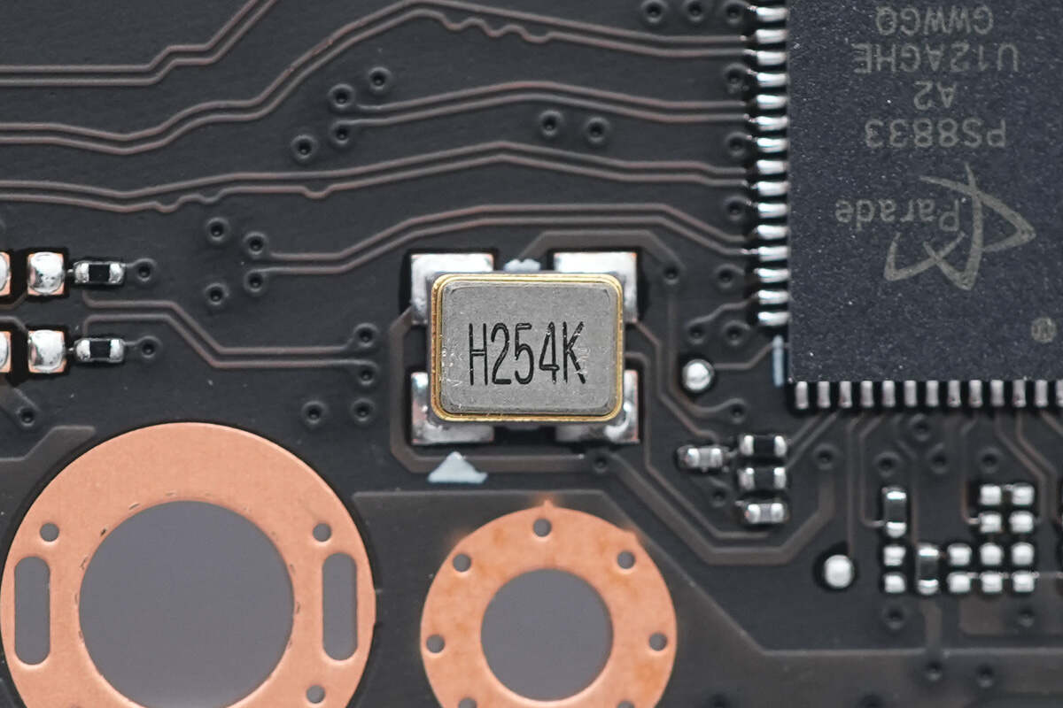
The retimer is from Parade. It supports USB4 at 40 Gbps and 20 Gbps, as well as DP and Thunderbolt Alt modes, and DP2.1 video output. It comes in a QFN62 package. Model is PS8833.
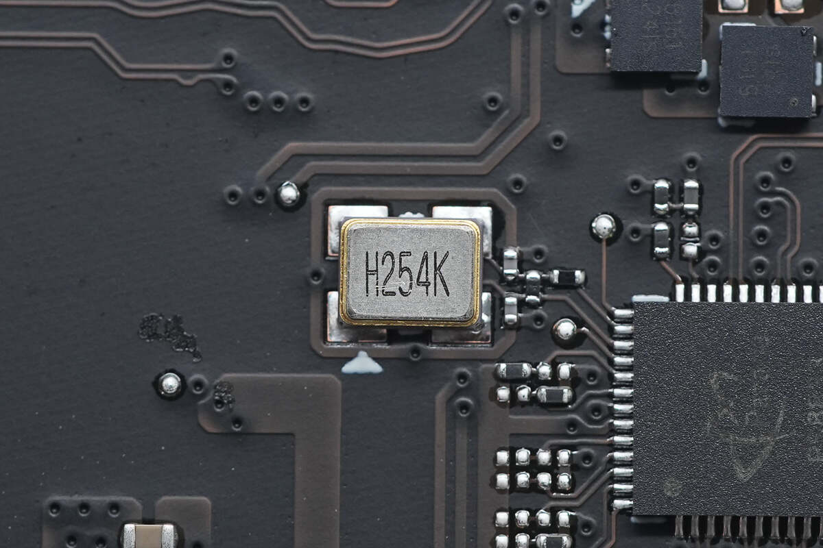
The chip is paired with an external 25.000 MHz SMD crystal oscillator.
A close-up of the other Parade PS8833 retimer, with two chips used to manage each of the two USB-C ports.
The chip is paired with an external 25.000 MHz SMD crystal oscillator.
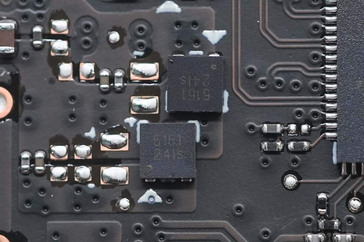
The two TVS diodes are from OmniVision, with a working voltage of 24V. They are used to absorb overvoltage surges and provide overvoltage protection for the USB-C ports. The diodes come in a DFN 2x2-3L package. Model is ESD56161D-24.
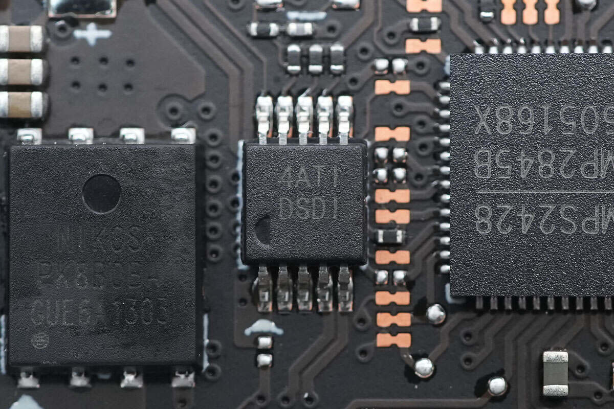
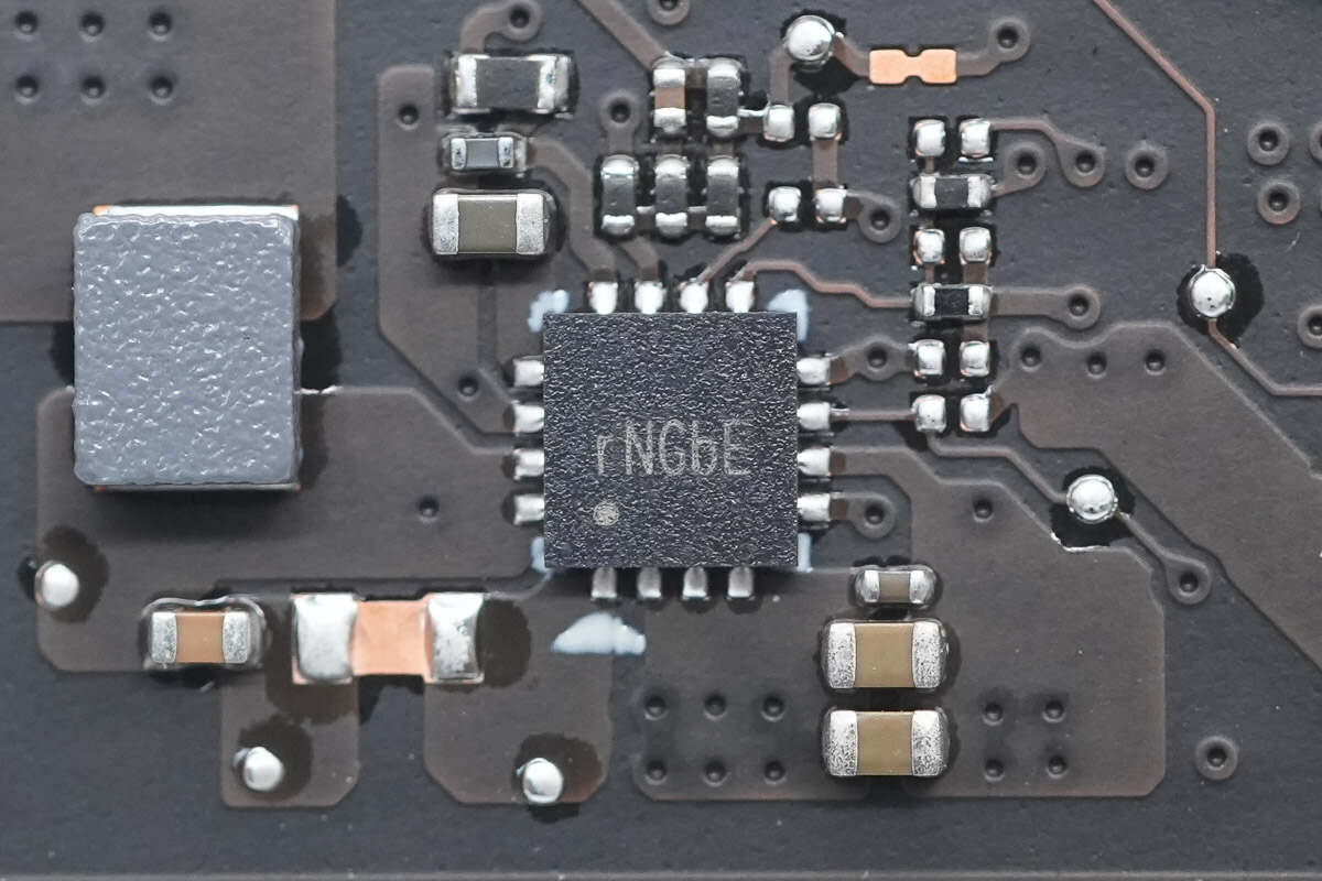
The temperature sensor, marked with DSDI, is from TI. It supports two external channels and local temperature detection, providing three channels of temperature monitoring with an accuracy of ±1°C. Communication is via the SMBus serial interface, and it comes in a VSSOP-10 package. Model is TMP432.
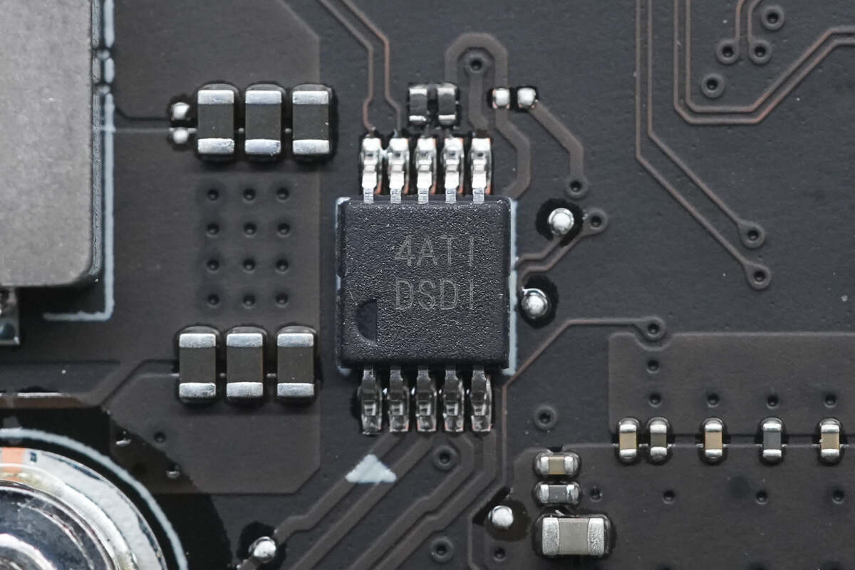
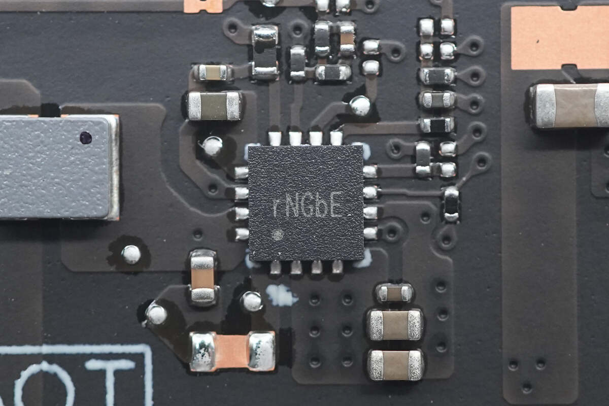
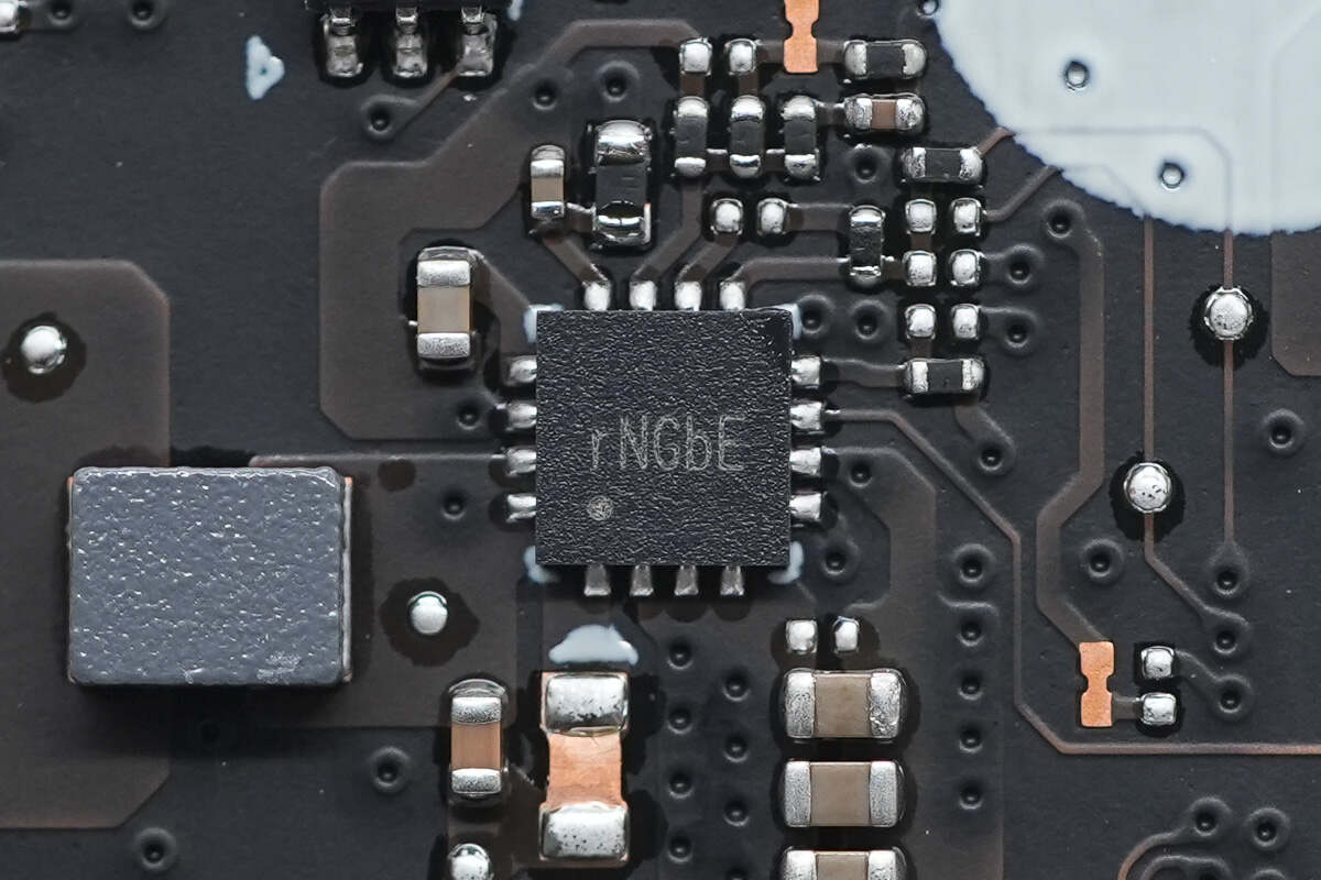
A close-up of the other sensor of the same model.
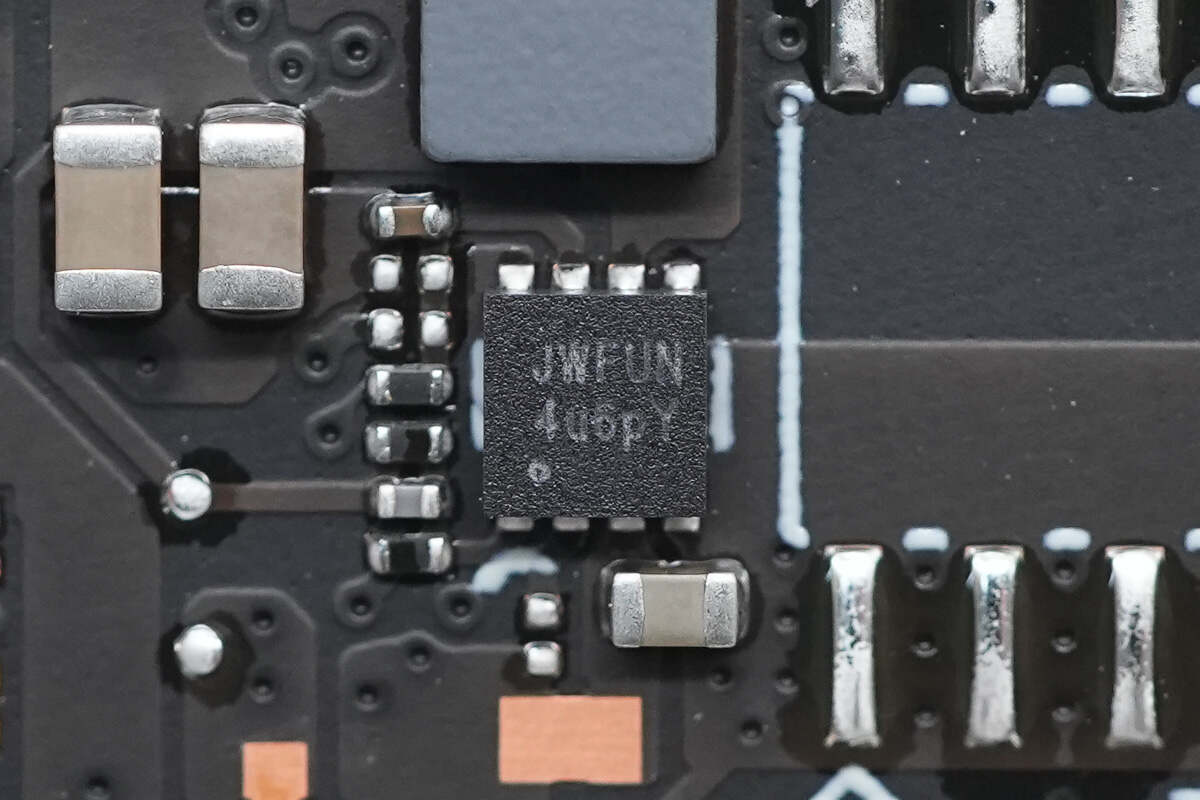
The synchronous buck chip, marked with JWFU, is from JOULWATT. It supports an input voltage range of 2.5-6V and provides a 3A output current. The chip integrates the switch MOSFET and operates at a switching frequency of 1 MHz. It features input undervoltage lockout, overcurrent protection, overvoltage protection, and overtemperature protection, and comes in a DFN 2x2 package. Model is JW5213L.
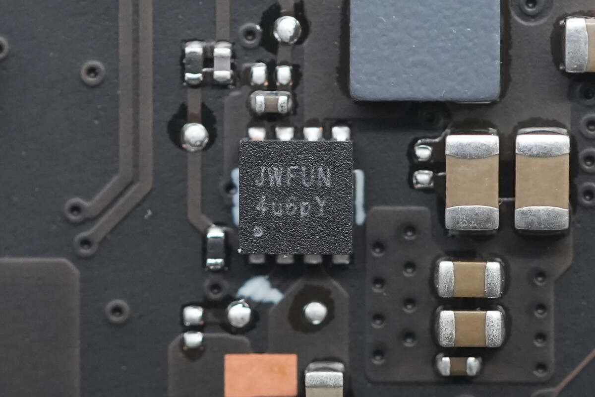
Close-up of the JOULWATT JW5213L synchronous buck chip.
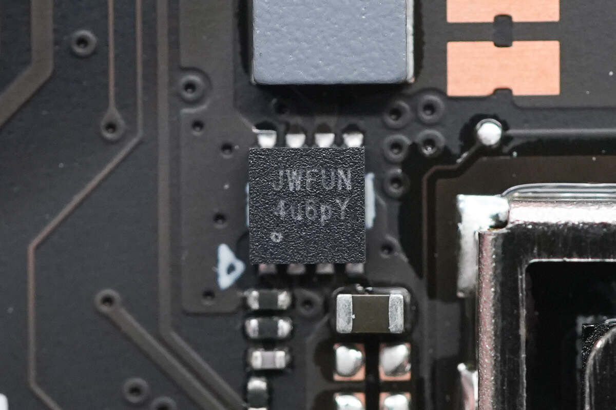
A total of three JOULWATT JW5213 synchronous buck chips are used.
This synchronous buck chip is from Silergy. It supports an input voltage of 24V and provides a 6A output current. The chip integrates 38/19mΩ MOSFETs, features output indication and discharge, and offers cycle-by-cycle valley and peak current limiting. It also includes self-resetting output overvoltage protection and comes in a QFN16 package. Model is SY8386A.
Close-up of the Silergy SY8386A synchronous buck chip.
A total of three Silergy SY8386A synchronous buck chips are used.
The LPDDR5 memory power supply chip is from TI and comes in a VQFN18 package. Model is TPS51488.
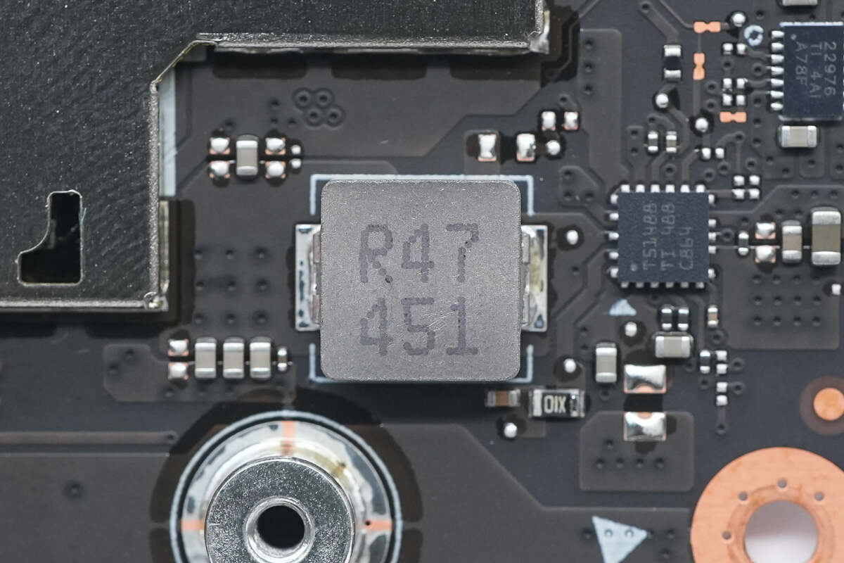
Close-up of the 0.47μH buck inductor used in conjunction.
The synchronous buck chip is from Silergy. It is a high-efficiency synchronous buck converter that supports a 24V input voltage. The chip integrates 18/8mΩ MOSFETs and provides a fixed output voltage of 3.36V with a 10A output current capability. It comes in a QFN 3x4-13 package. Model is SY8371B.
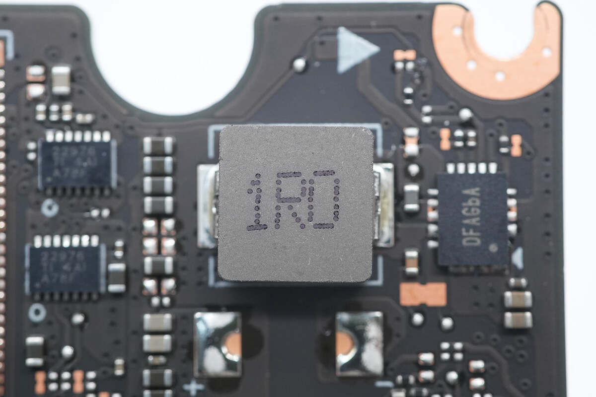
Close-up of the 1μH buck inductor used in conjunction.
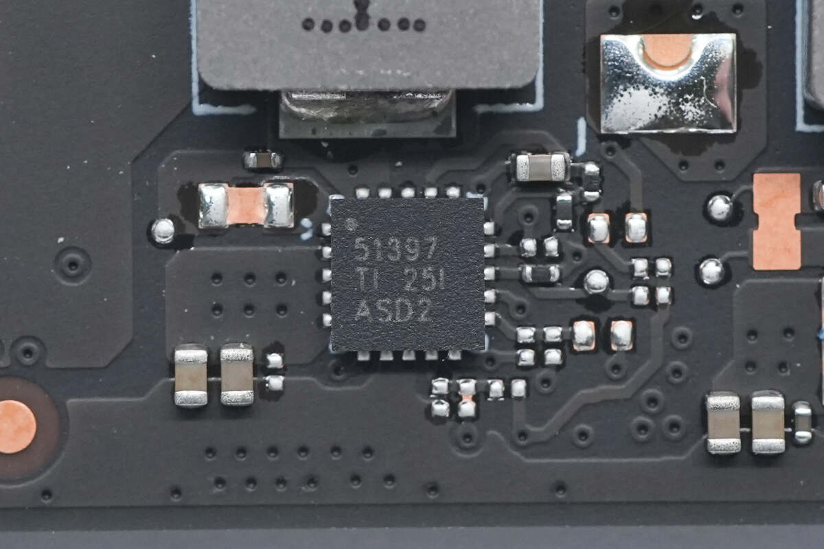
The synchronous buck chip is from TI and adopts the VQFN-20 package. Model is TPS51397.
Close-up of the 0.68μH buck inductor used in conjunction.
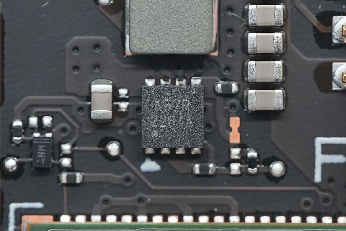
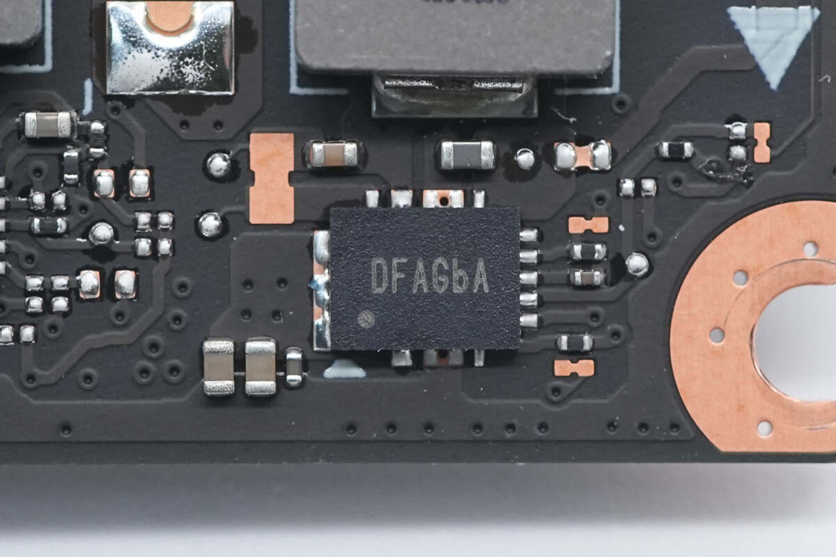
This chip is marked with A37R.
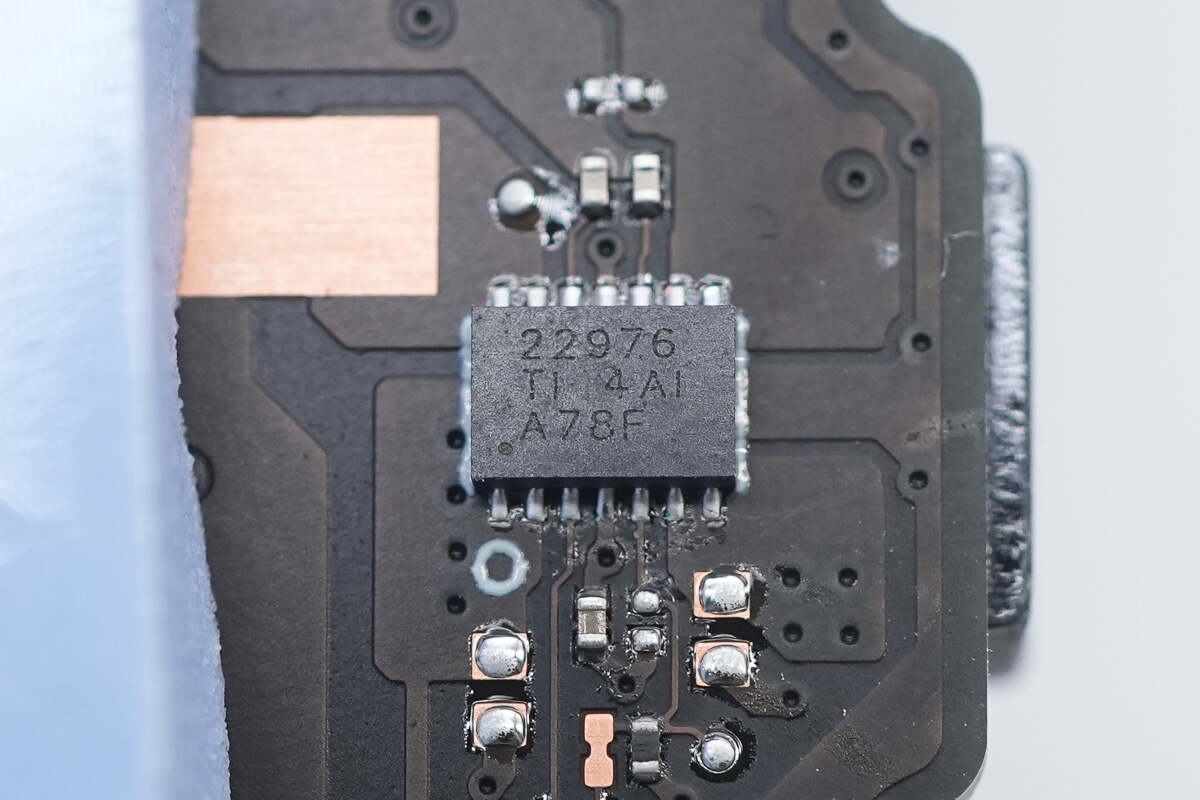
The load switch is from TI. The chip features two internal channels, supports 5V applications, and provides a maximum continuous current of 6A. It comes in a WSON14 package. Model is TPS22976.
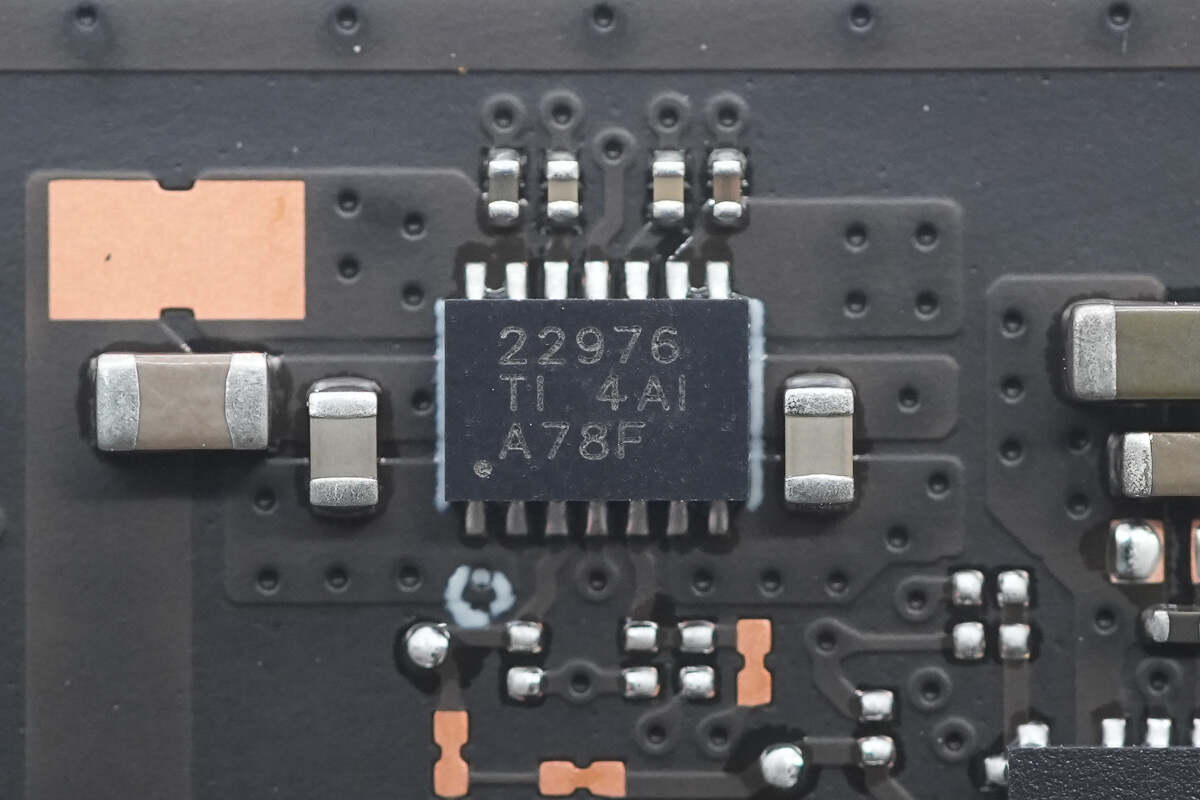
A close-up of the other TPS22976 load switch.
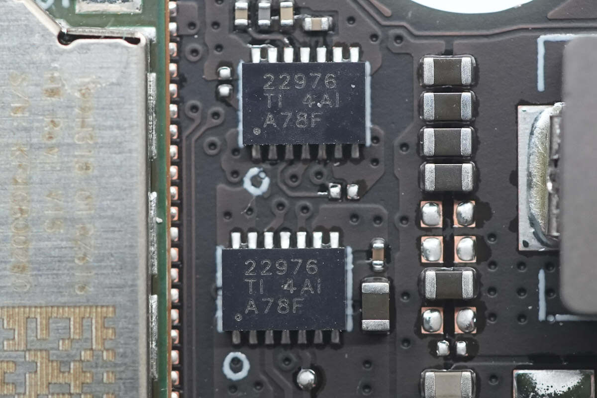
A total of four TPS22976 load switches are used.
A thermal silicone pad is placed at the location corresponding to the SSD.
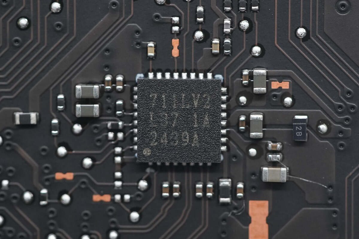
The card reader chip is from BayHub. It supports PCIe to TF interface and comes in a QFN32 package. Model is OZ711LV2.
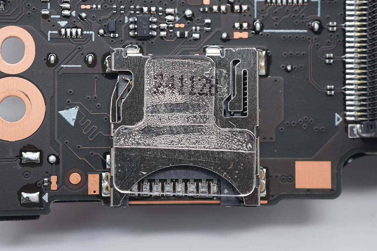
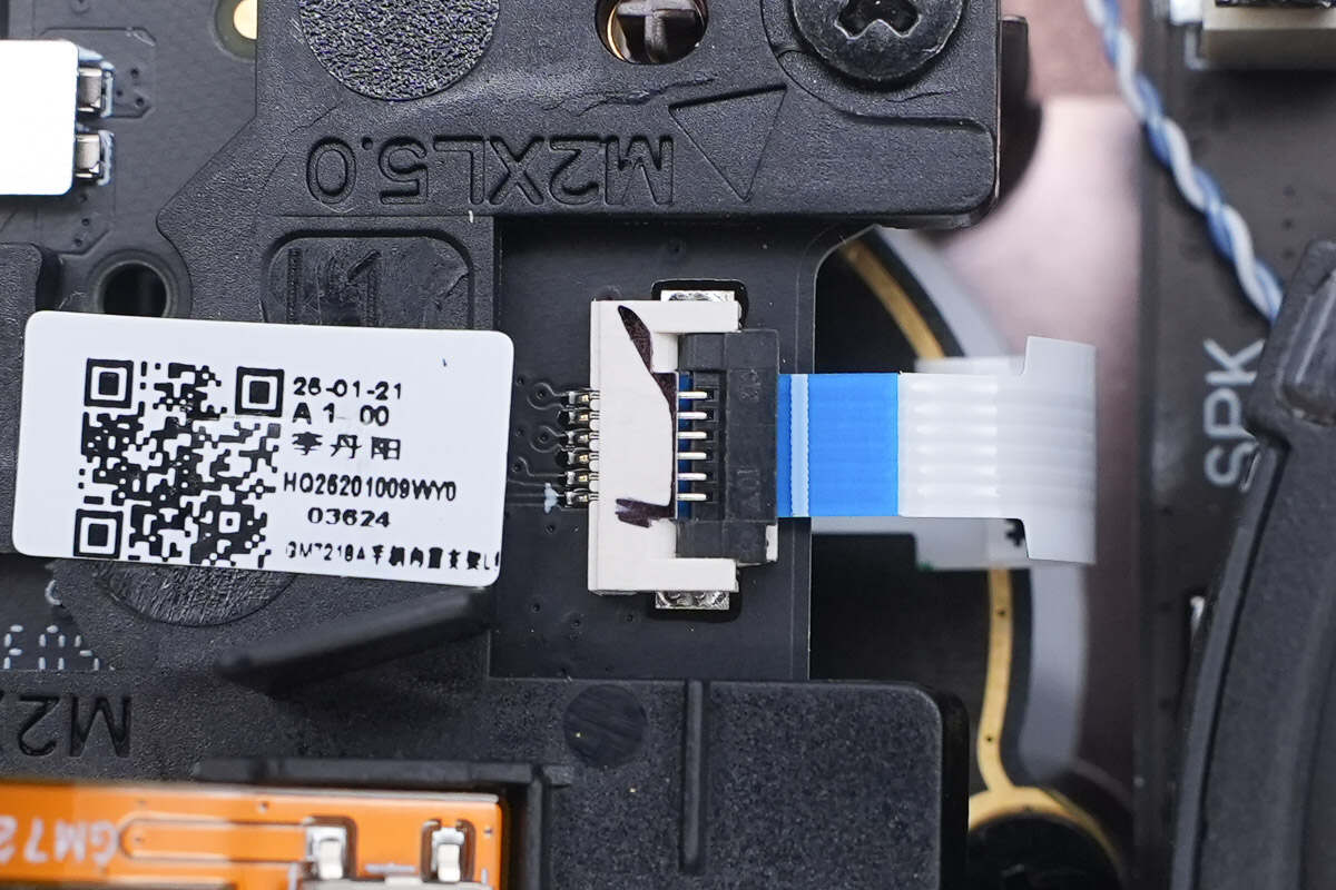
Close-up of the TF card slot, which supports up to 2TB of expansion.
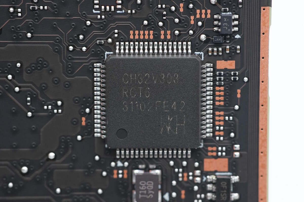
The MCU is from WCH. It is an industrial-grade general-purpose enhanced MCU based on a 32-bit RISC-V instruction set and architecture. It integrates 64KB of SRAM and 256KB of Flash, operates at a main frequency of 144 MHz, and features interfaces such as I2C, I2S, SPI, USART, SDIO, and CAN controller. It comes in an LQFP64M package. Model is CH32V303RCT6.
Close-up of the external 16MHz clock crystal oscillator for the MCU.
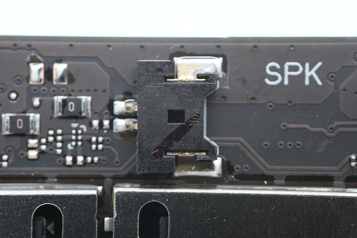
Close-up of the connector for the left-side speaker.
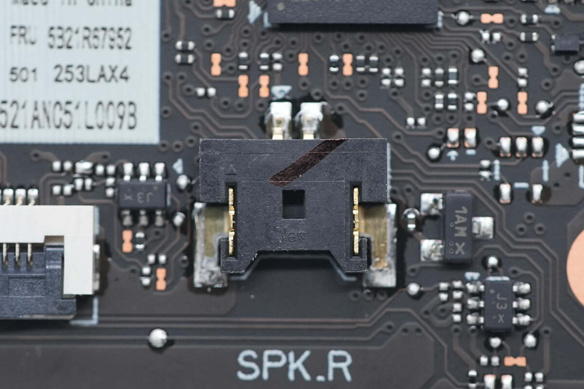
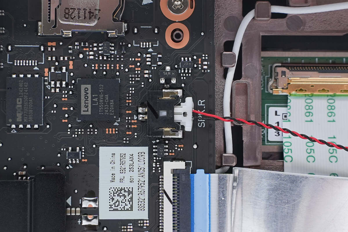
Close-up of the connector for the right-side speaker.
Close-up of the connector for the volume button flex cable.
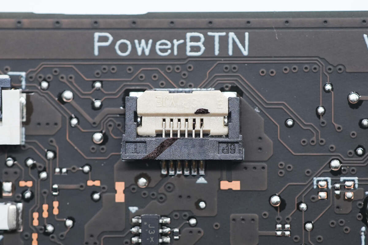
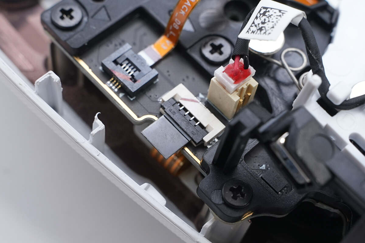
Close-up of the power button flex cable socket.
Close-up of the connector for the power button flex cable.
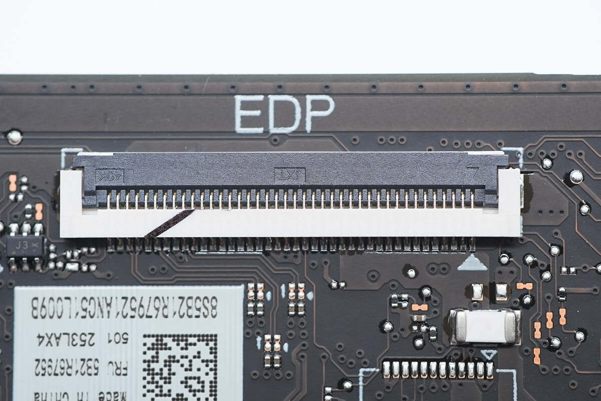
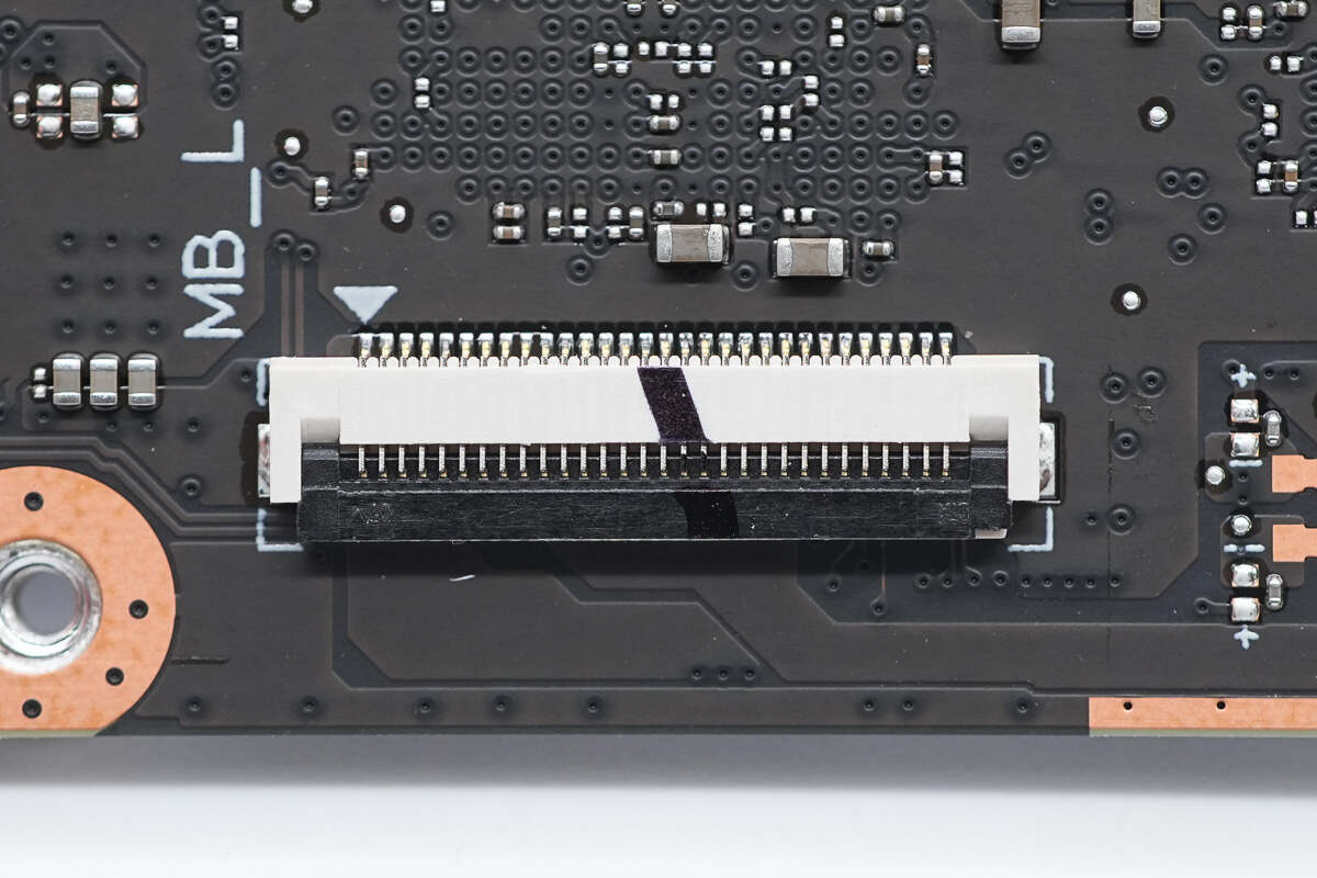
Close-up of the connector for the screen eDP cable.
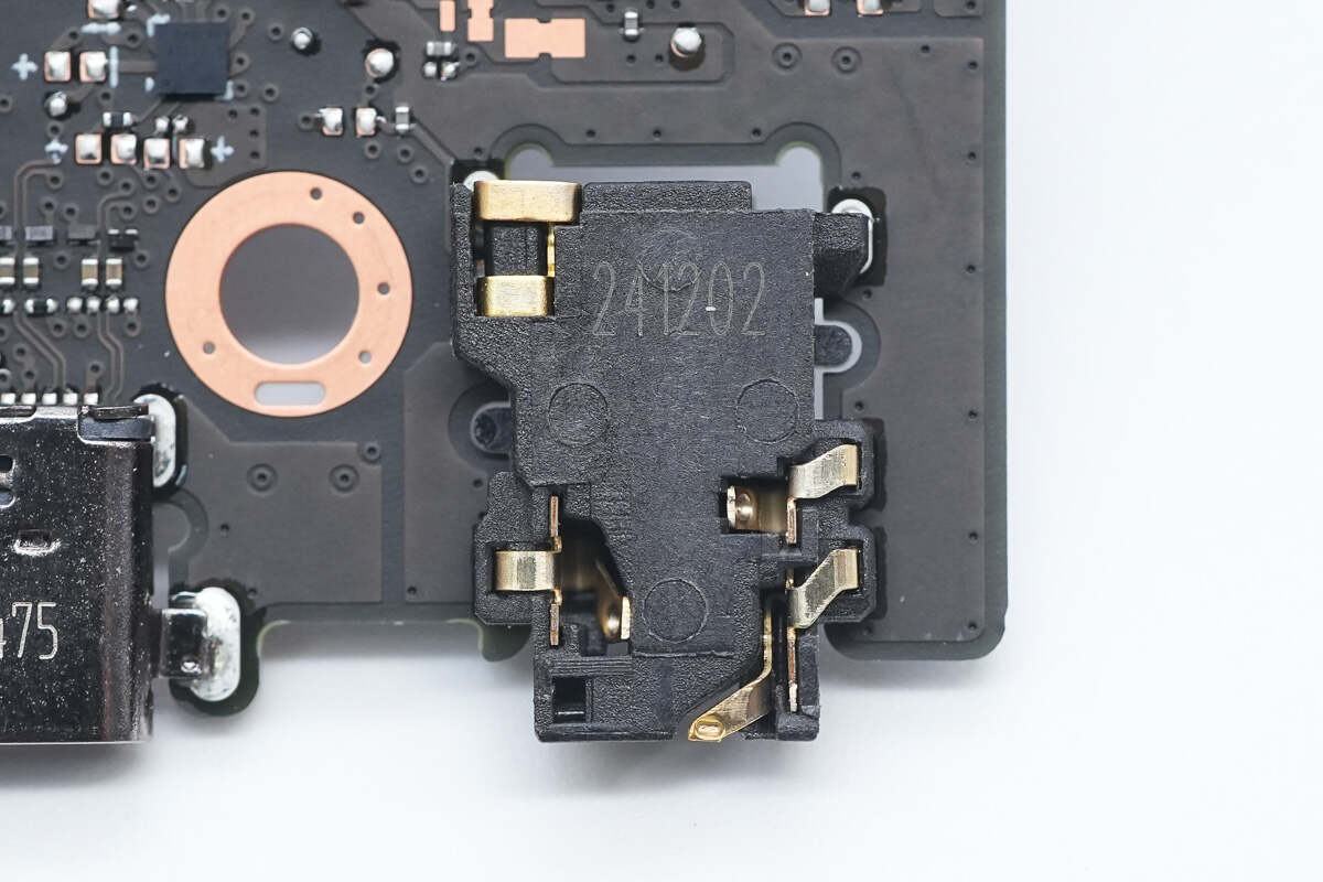
Close-up of the 3.5mm audio jack.
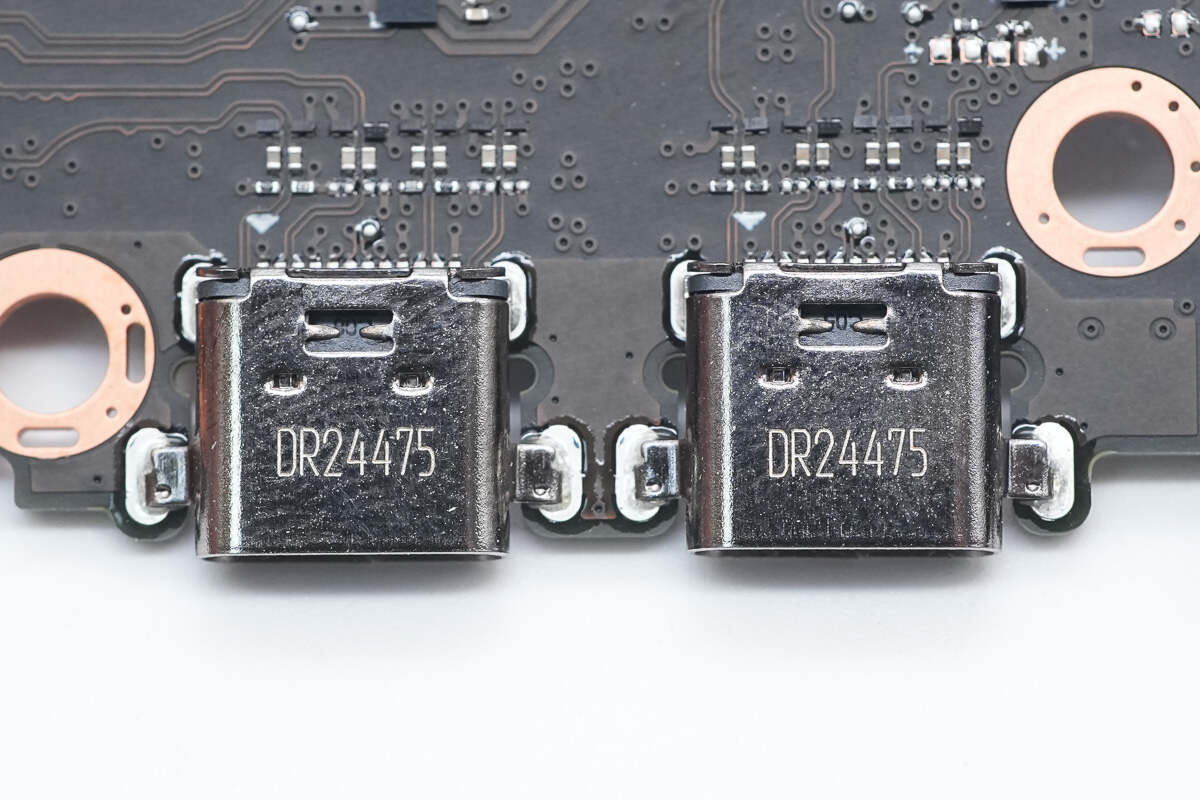
Close-up of two USB-C ports, fixed with through-hole soldering.
Close-up of the battery connector.
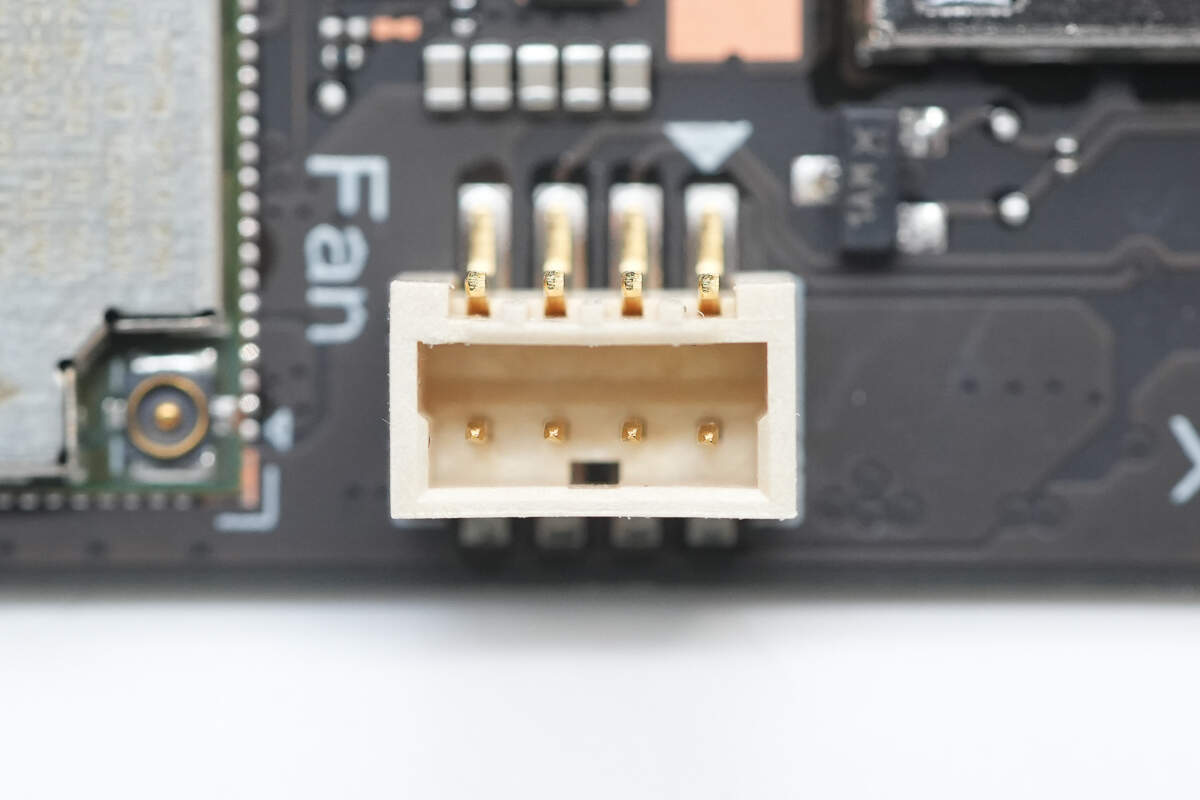
Close-up of the fan connector.
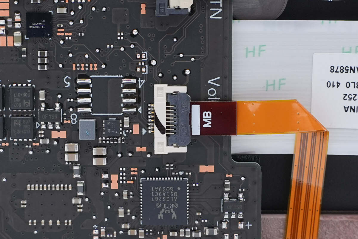
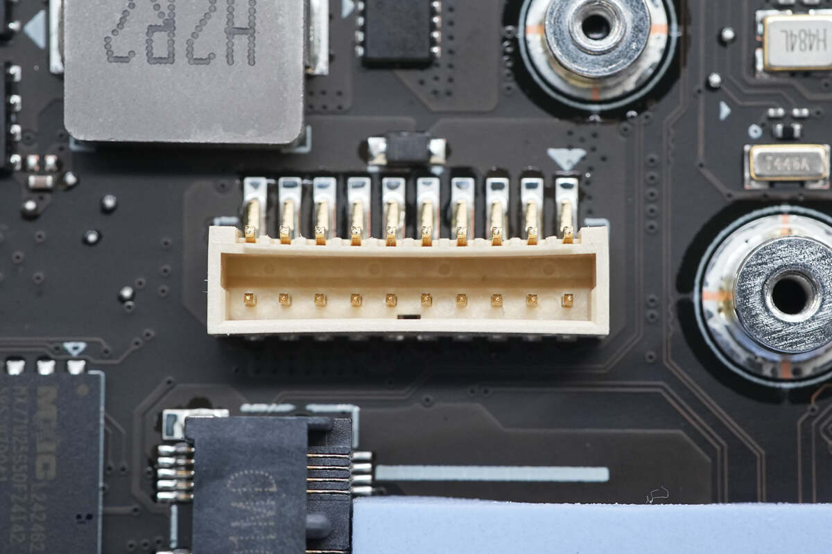
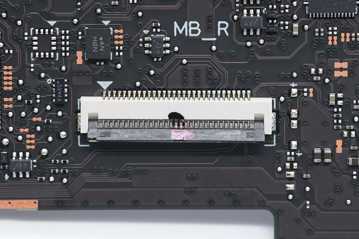
Close-up of the ribbon cable connector on the secondary board.
Close-up of the ribbon cable connector on the right-side secondary board.
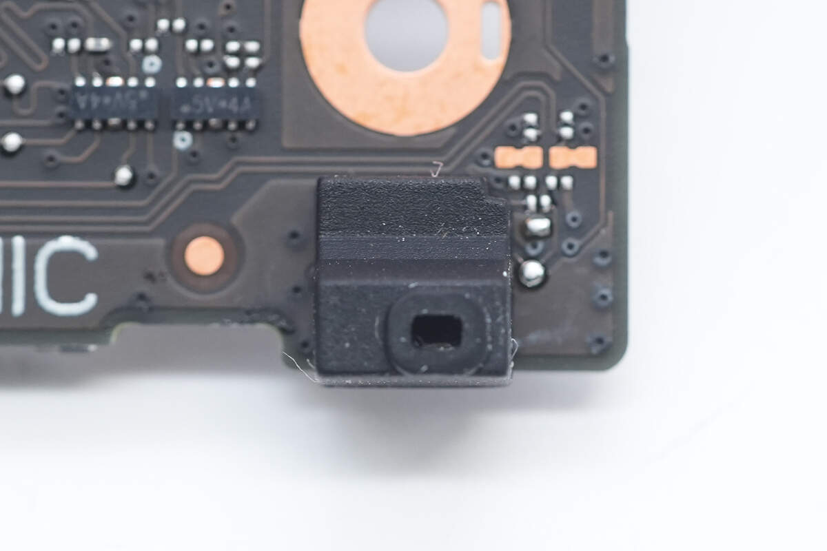
The microphone is covered with a sealing rubber sleeve.
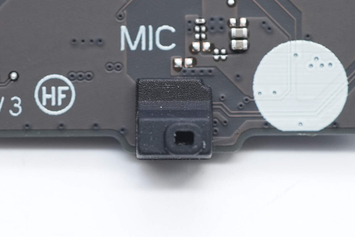
The other microphone is also covered with a sealing rubber sleeve.
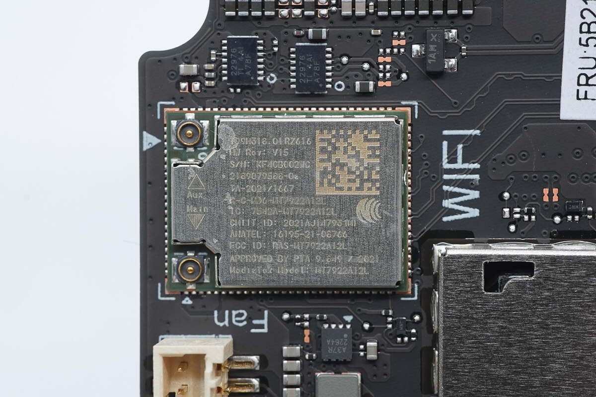
The wireless network card features a built-in MediaTek MT7922 wireless chip. Model is RZ616.
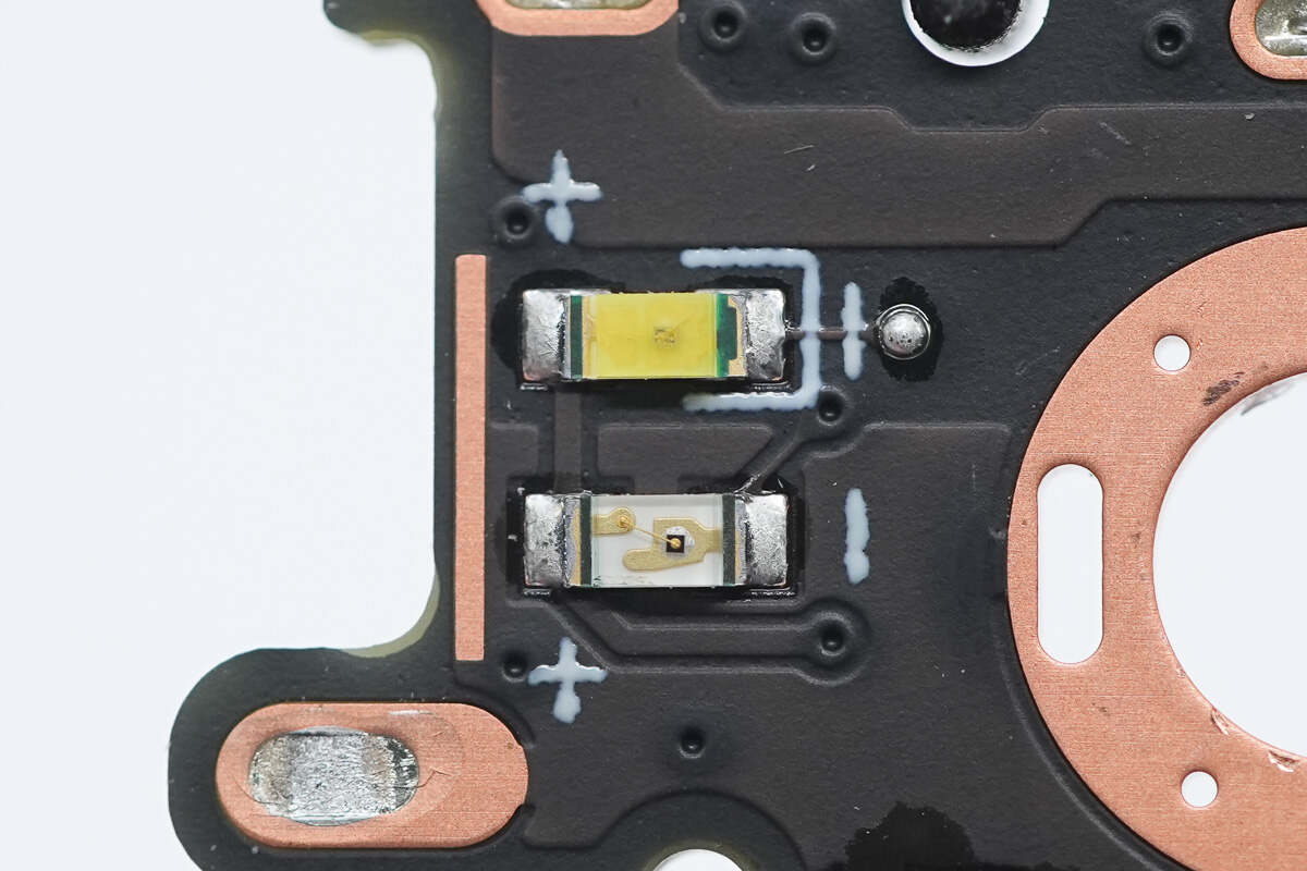
Two SMD LEDs are used to indicate the charging status.
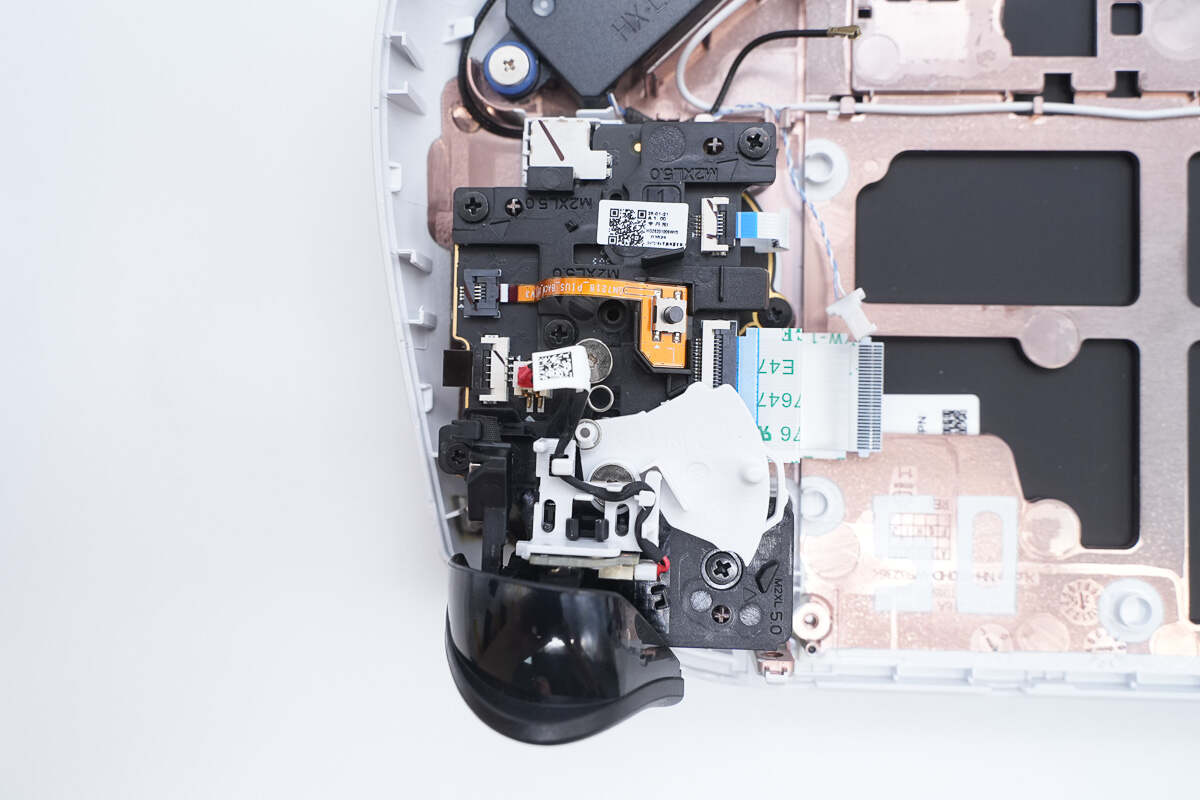
Next, we will disassemble the shoulder buttons, regular buttons, and joystick mechanisms on both sides.
First, remove the shoulder buttons.
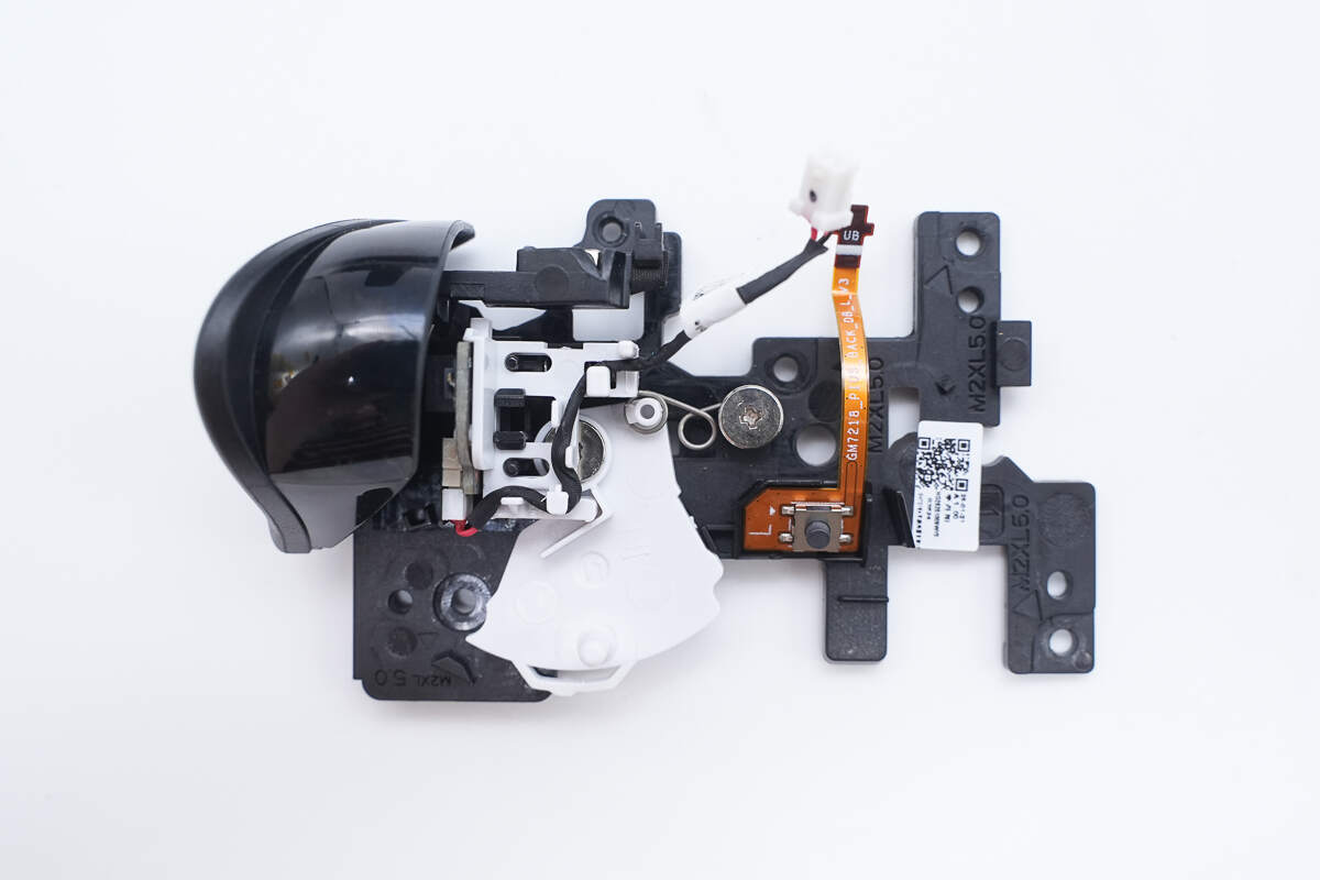
The shoulder button mechanism includes a range switch and a control button.
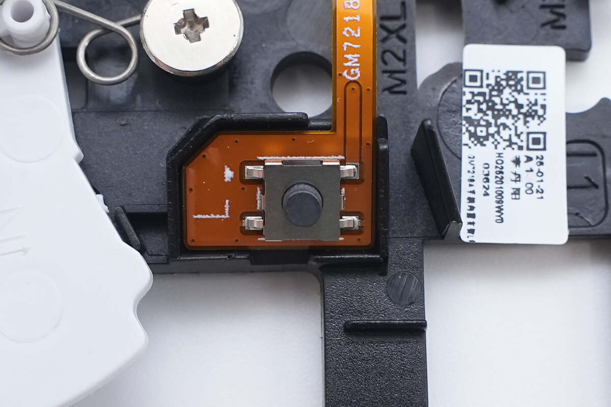
Close-up of the micro switch for the control button.
The shoulder button micro switch is mounted on a separate small PCB and connected via wires.
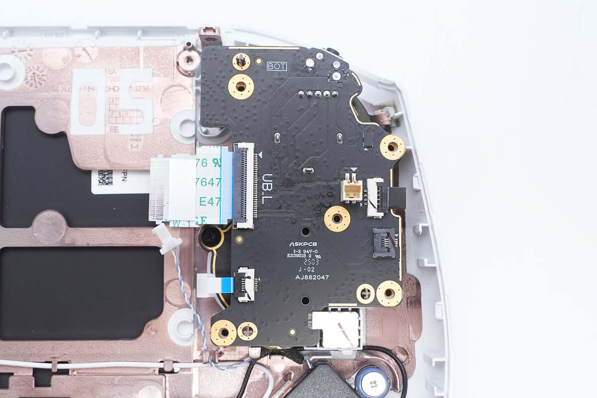
The secondary board features multiple ribbon cable connectors for connecting buttons and RGB LEDs.
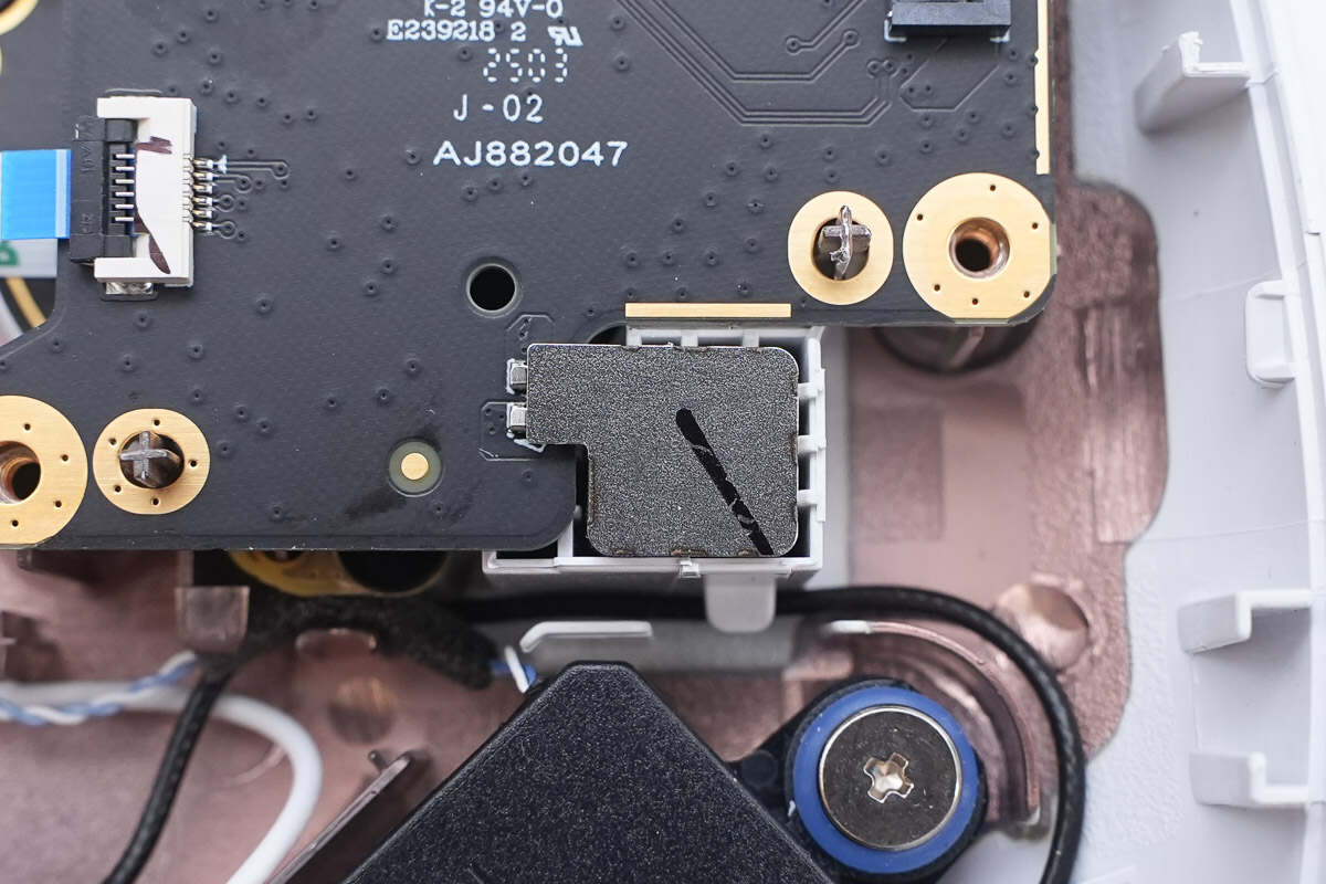
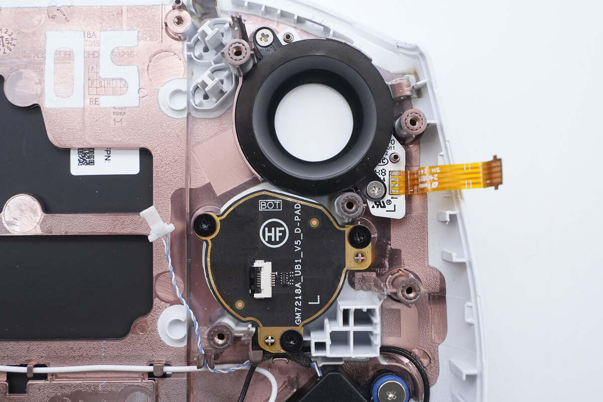
Close-up of the built-in linear motor.
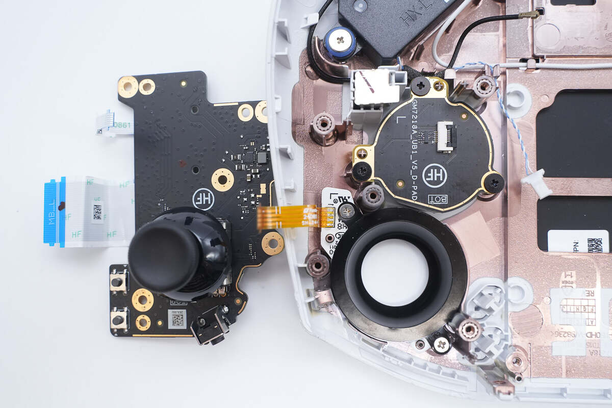
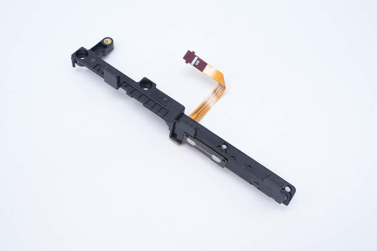
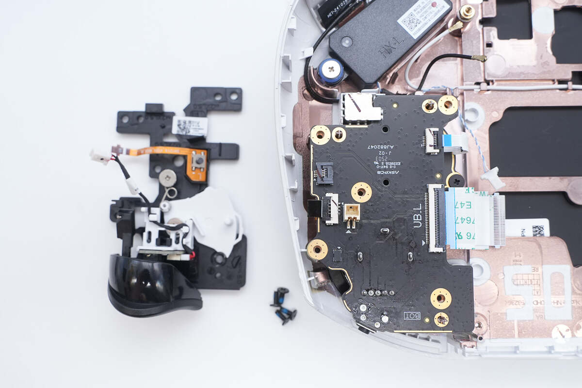
After removing the side secondary board, you can see that the joystick and shoulder buttons are mounted on the board, while the directional pad is fixed to the outer shell.
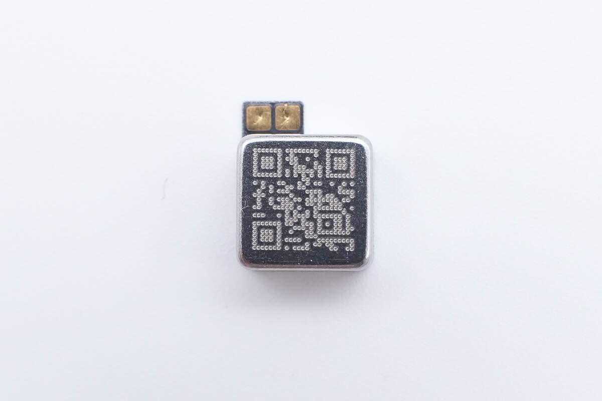
The housing of the linear motor has a QR code printed on it.
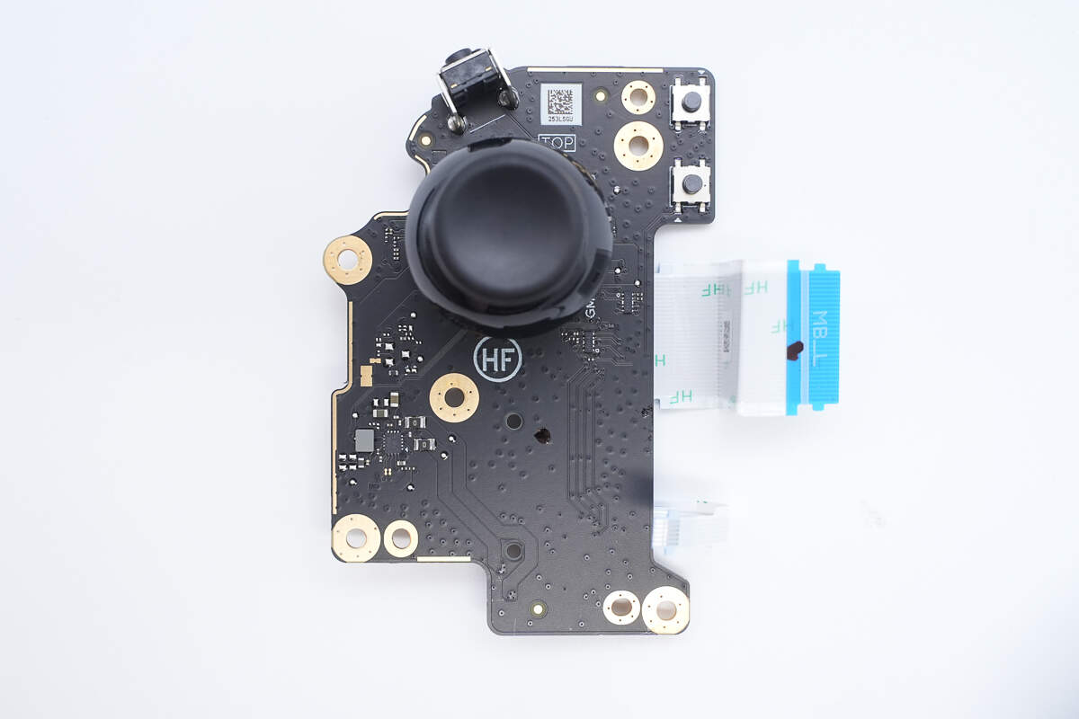
In the upper left corner of the secondary board is a shoulder button, below it is the joystick, and function buttons are located on the right side.
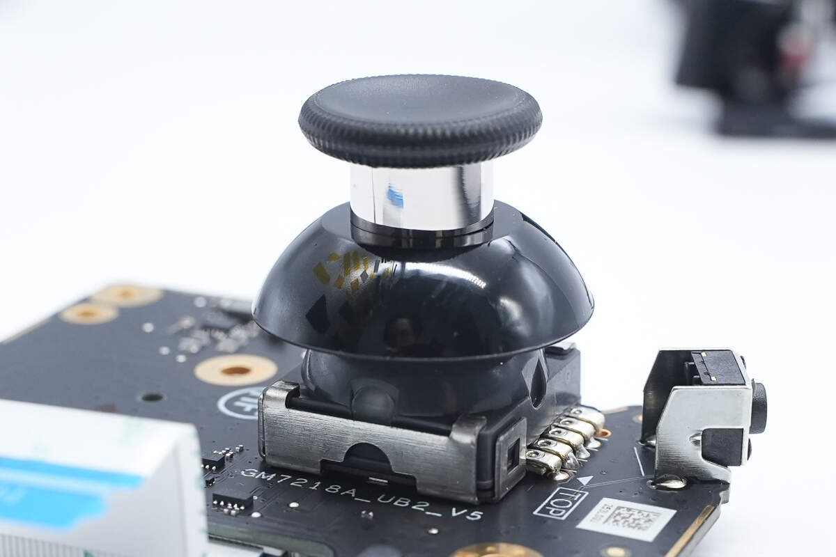
The joystick is secured through through-hole soldering.
Close-up of the Legion L button and the view button.
The shoulder buttons are secured through through-hole soldering.
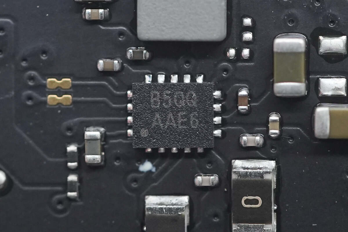
The linear motor driver marked with B5QQ is from awinic. The chip integrates a high-voltage H-bridge driver and a synchronous boost converter. It can be configured via an I2C interface and features three hardware trigger inputs. The chip comes in an FCQFN-18L package. Model is AW86937FCR.
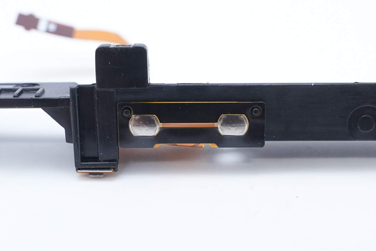
The back side of the secondary board is also equipped with a Hall sensor to detect the trigger position.
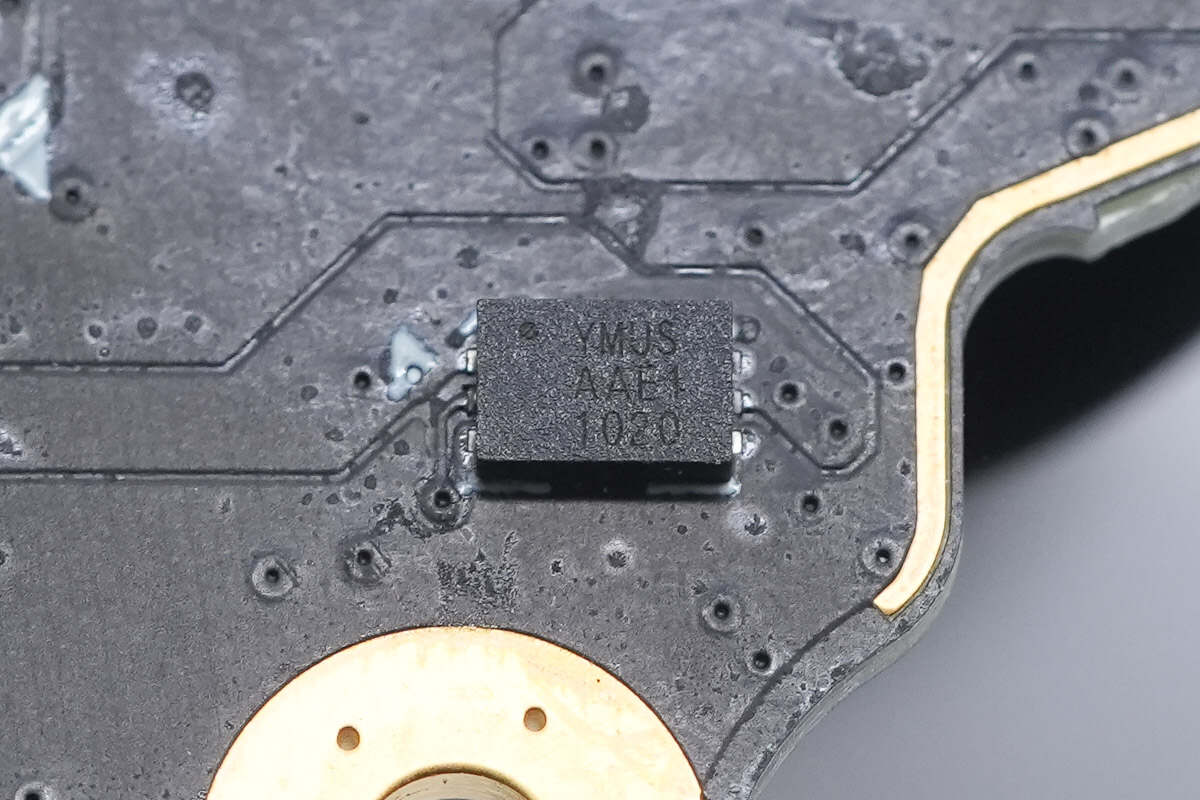
The Hall sensor marked with YMUS is from Awinic. It is a high-sensitivity linear Hall sensor and comes in a DFN-6 package. Model is AW86561DNR.
Close-up of the RGB LED ring and the small PCB for the button.
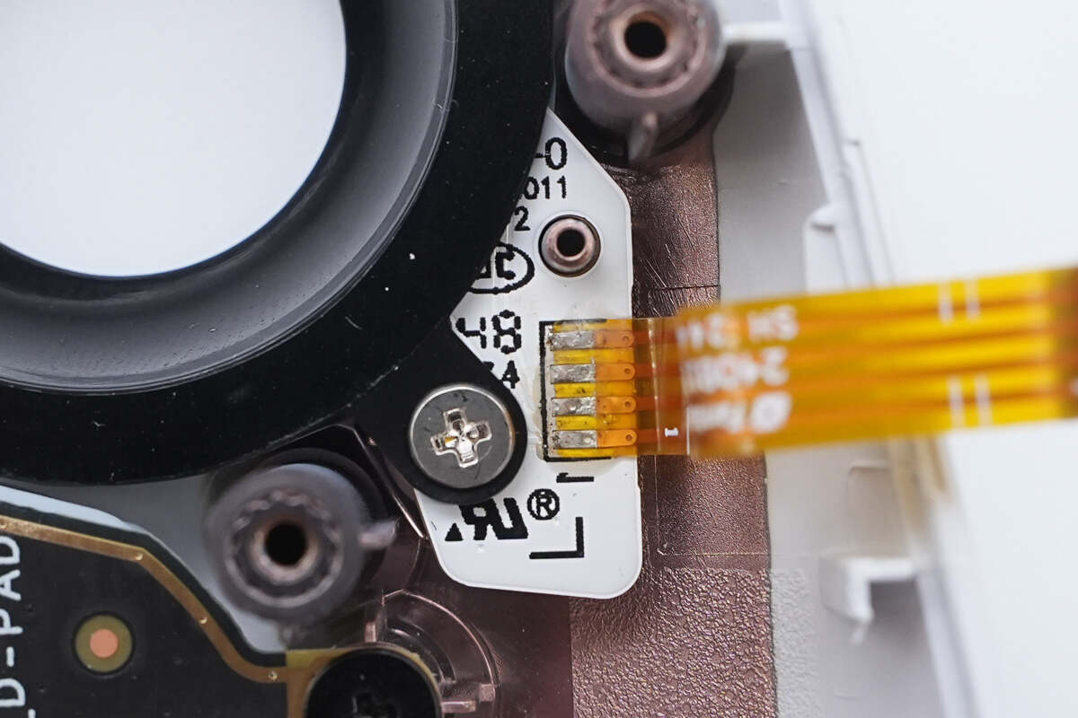
The RGB LED ring is connected via soldered ribbon cables.
The small PCB for the button is connected using a ribbon cable connector.
Well, those are all components of the Lenovo Legion Go S Gaming Console.
Summary of ChargerLAB
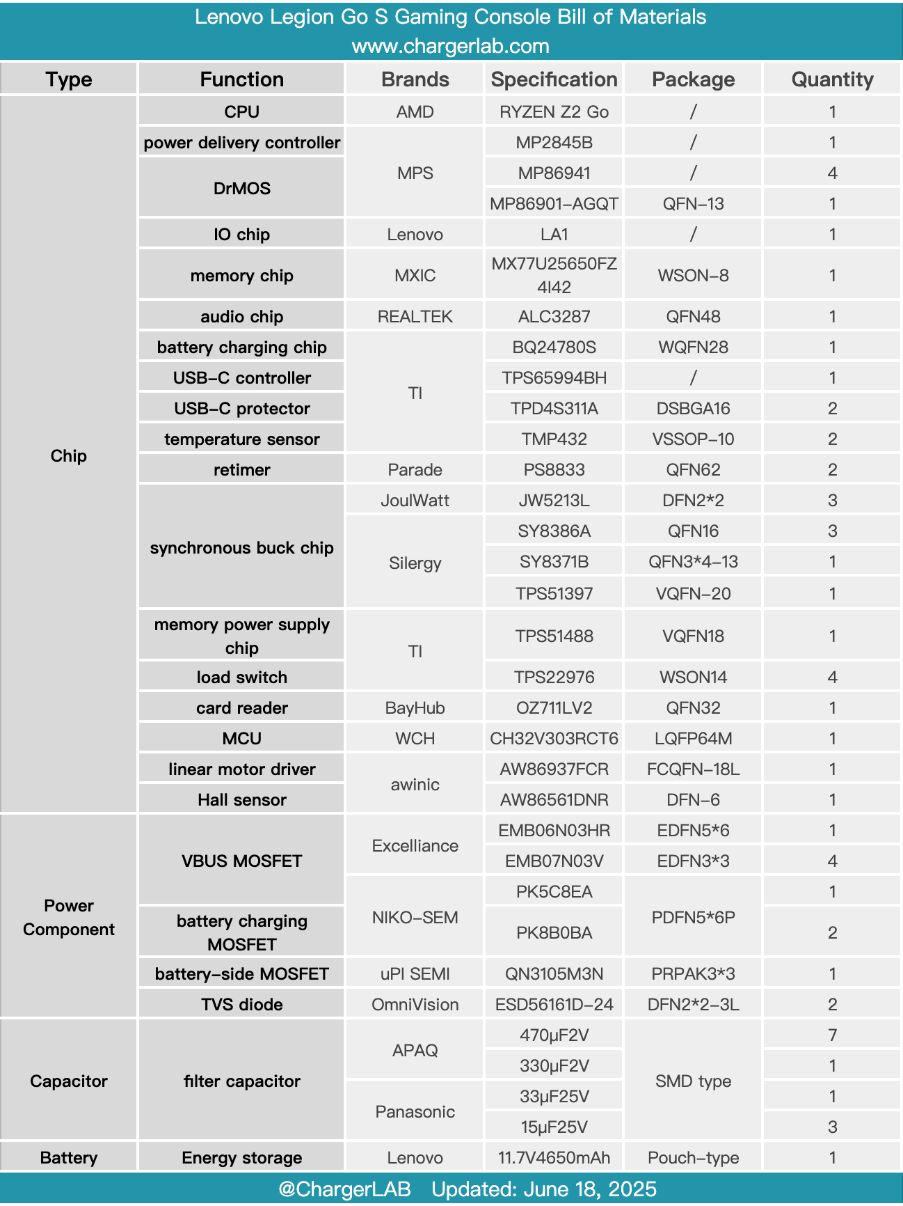
Here is the component list of the Lenovo Legion Go S Gaming Console for your convenience.
It features an 8-inch 120Hz high refresh rate display, with Hall-effect joysticks and Hall-effect shoulder buttons on both sides of the screen, along with a directional pad and function buttons for convenient gaming controls. It offers dual USB4 ports, supporting 100W charging and 4K 120Hz video output, making it easy to connect to external power sources, displays, and storage devices.
After taking it apart, we found that it is equipped with an AMD Ryzen Z2 Go processor and uses MPS power management chips along with DrMOS. The audio codec chip is from Realtek. The internal USB-C interface controller, port protection chip, and battery charging chip are all from TI.
The USB-C retimer is from Parade, and the synchronous buck converters are from JOULWATT and Silergy. For the CPU power supply, SMD capacitors from APAQ and Panasonic are used. There are secondary boards on both sides inside the device, connected to the mainboard via ribbon cables. Components such as the battery pack and cooling fan are also connected through plug-in connectors, which facilitate assembly and manufacturing.
Related Articles:
1. Unboxing of Lenovo Legion Go S
2. Charging Review of Lenovo Legion Go Handheld Game Console
3. How Fast Is Lenovo Legion Go Charged? - ChargerLAB Compatibility 100