Chargerlab Chargerlab
  • News
    • What's New
    • Interviews
    • Vlogs
    • Events
    • Industry
  • Reviews
    • Charging Compatibility
    • Fully Charging
    • Comparison
    • Chargers & Cables
    • Power Banks & Stations
    • Mobile Devices
    • Accessories
  • Teardowns
    • Chargers & Cables
    • Power Banks & Stations
    • Power Supplies
    • Prototypes
    • Batteries
    • Accessories
  • Videos
    • YouTube
    • TikTok
  • Guides
    • How to Buy
    • Explained
    • Deals
    • ICs
  • POWER-Z
    • KM003C/KM002C
    • KT002
    • Buy POWER-Z
    • Technical Support
  • Contact Us
Home › Teardowns › Chargers & Cables › Teardown of Infinix 180W USB-C GaN Charger (U1800XEA)
  • 1

Teardown of Infinix 180W USB-C GaN Charger (U1800XEA)

Rusell
August 1, 2024

Introduction

ChargerLAB this time got a 180W USB-C GaN charger from Infinix. This charger is equipped with European pins and a USB-C port. It can support a charging power of up to 20V9A 180W. It can provide fast charging for phones and laptops.

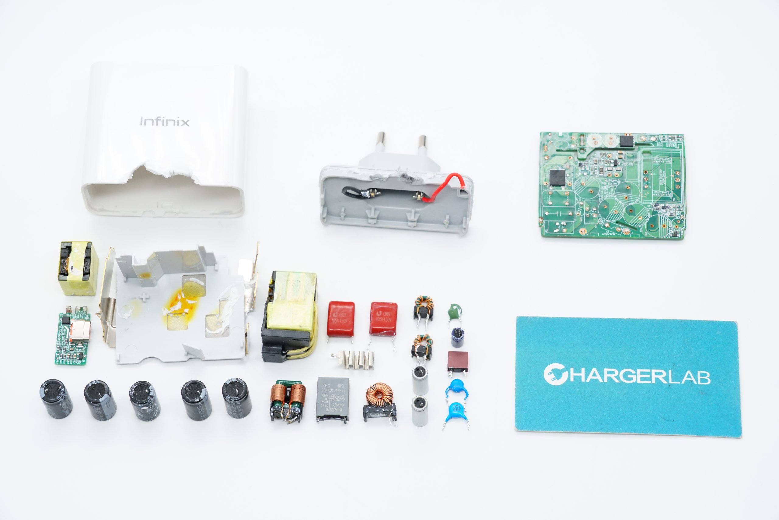
Next, we are going to take it apart to see its internal components and structure.

Product Appearance

Teardown of Infinix 180W USB-C GaN Charger (U1800XEA)-Chargerlab

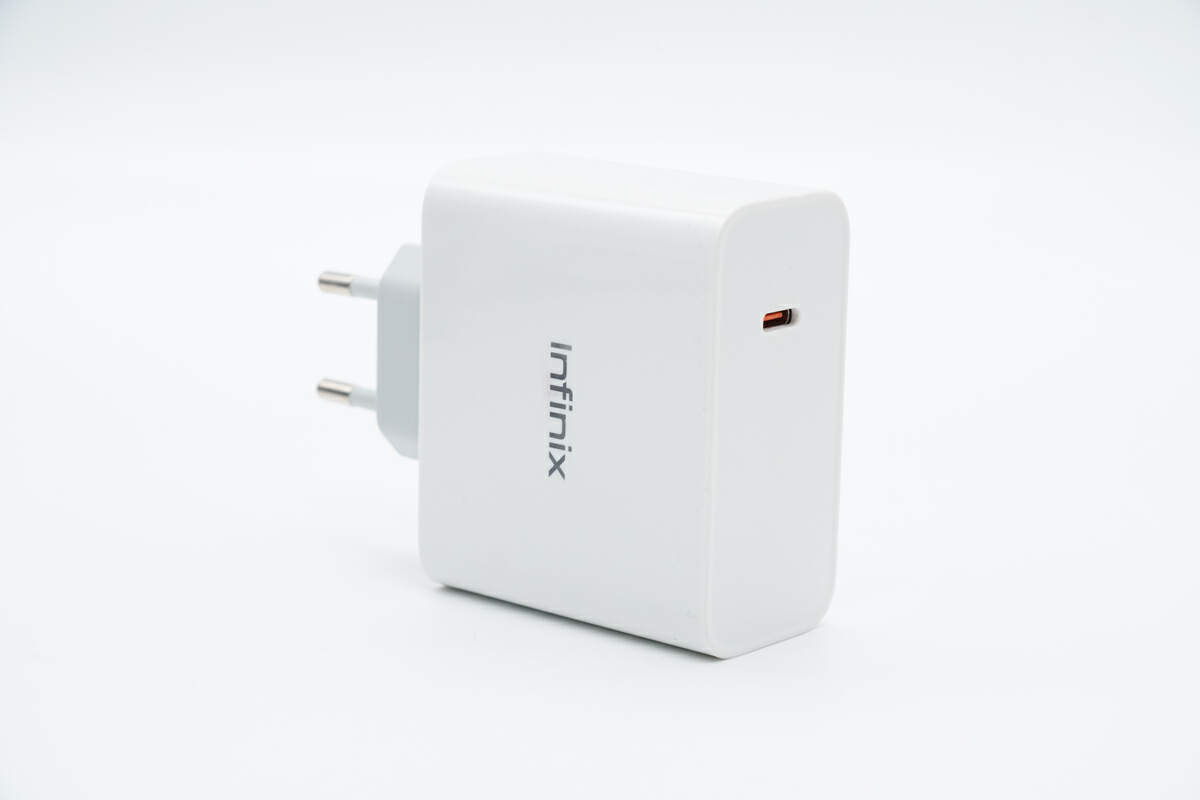
It adopts a one-piece white case.

Teardown of Infinix 180W USB-C GaN Charger (U1800XEA)-Chargerlab

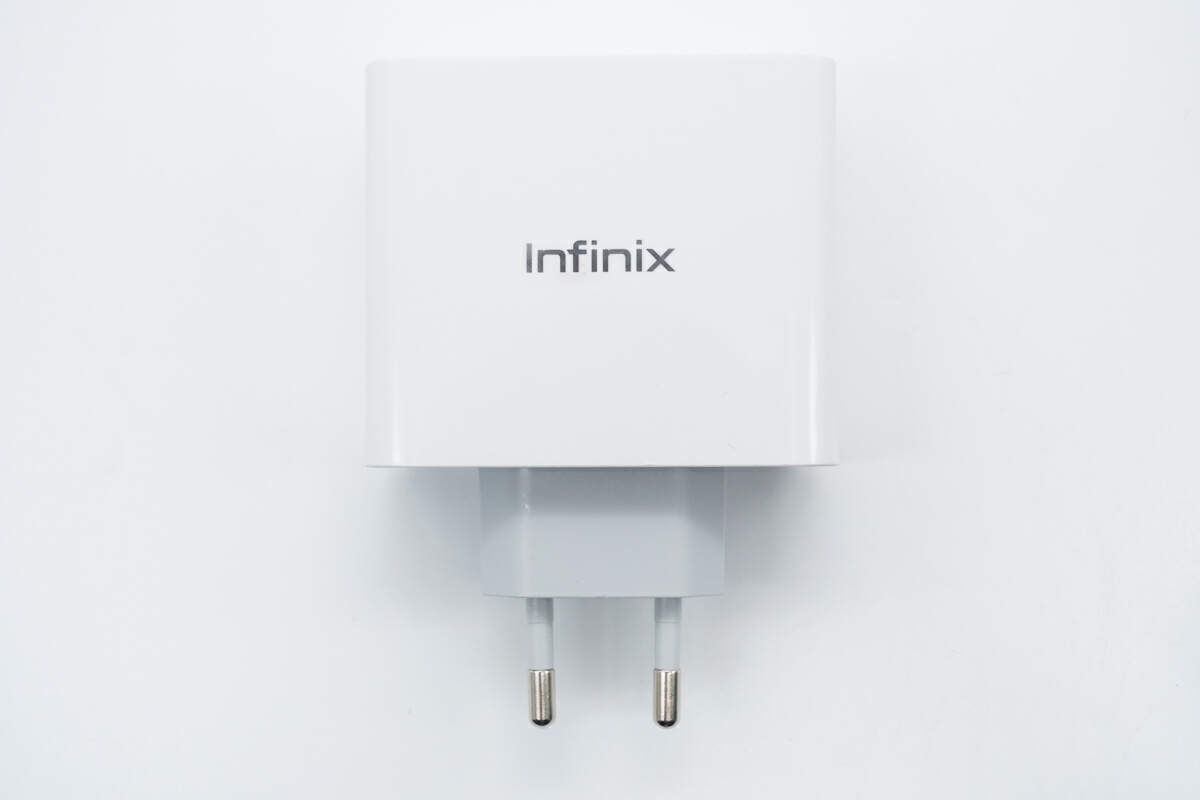
The "infinix" is printed in the middle.

Teardown of Infinix 180W USB-C GaN Charger (U1800XEA)-Chargerlab

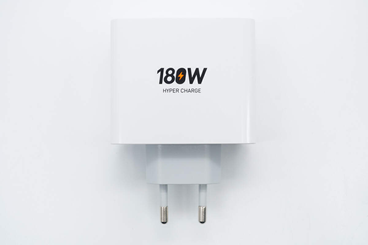
There is "180W HYPER CHARGE" printed on the center of the back.

Teardown of Infinix 180W USB-C GaN Charger (U1800XEA)-Chargerlab

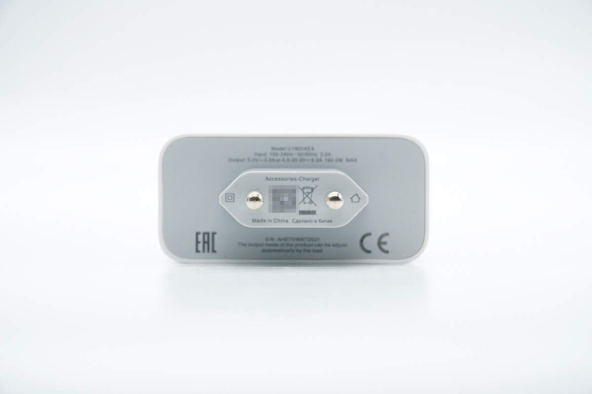
The specs info are printed on the input end. It has passed EAC and CE certifications.

Teardown of Infinix 180W USB-C GaN Charger (U1800XEA)-Chargerlab

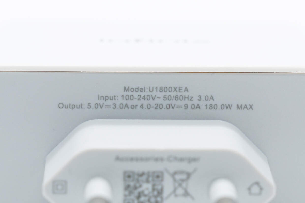
Model is U1800XEA. It can support input of 100-240V~50/60Hz 3A. And it can support output of 5V3A, and 4-20V9A. The maximum output power is 180W.

Teardown of Infinix 180W USB-C GaN Charger (U1800XEA)-Chargerlab

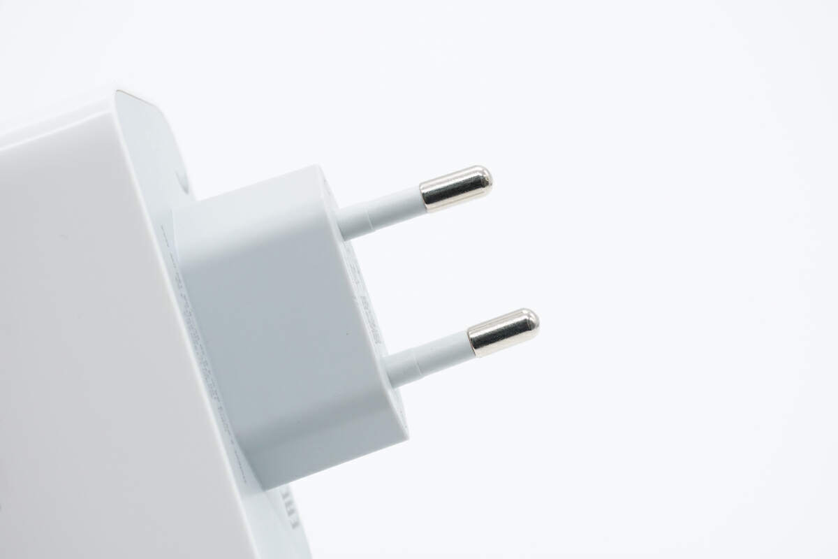
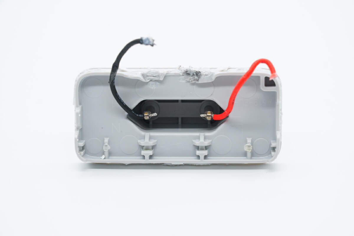
The charger is equipped with European pins.

Teardown of Infinix 180W USB-C GaN Charger (U1800XEA)-Chargerlab

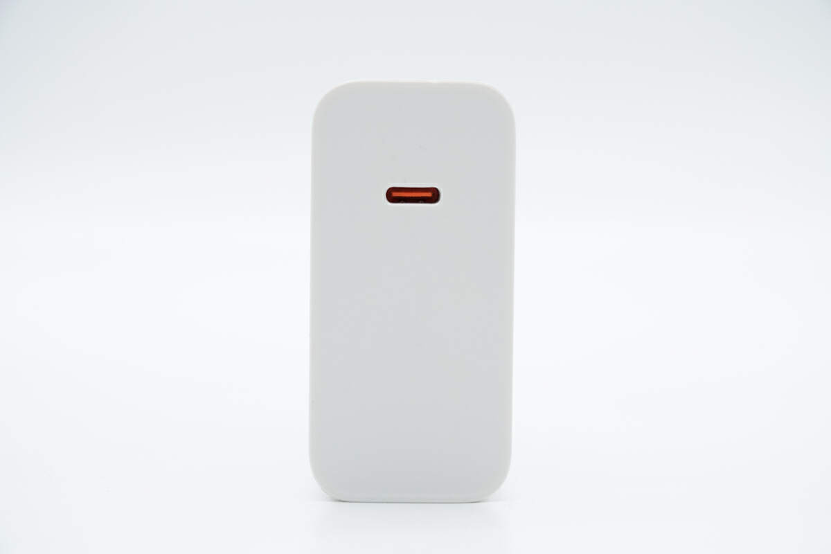
Here is the USB-C port. 

Teardown of Infinix 180W USB-C GaN Charger (U1800XEA)-Chargerlab

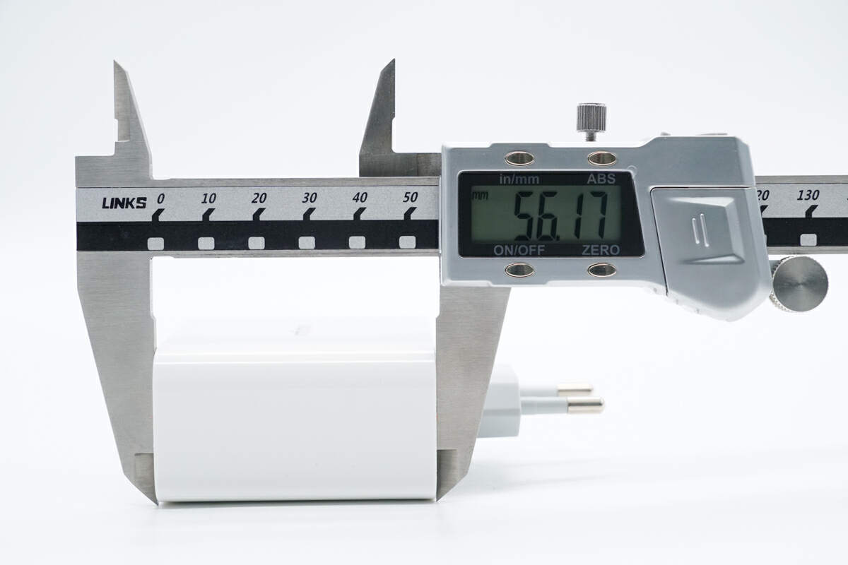
The height of it is about 56 mm (2.2 inches).

Teardown of Infinix 180W USB-C GaN Charger (U1800XEA)-Chargerlab

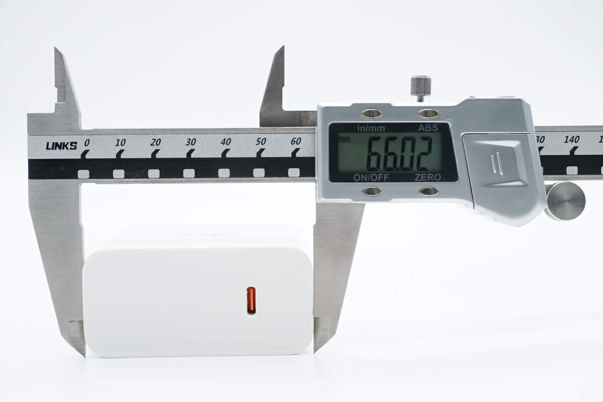
The width is about 66 mm (2.6 inches). 

Teardown of Infinix 180W USB-C GaN Charger (U1800XEA)-Chargerlab

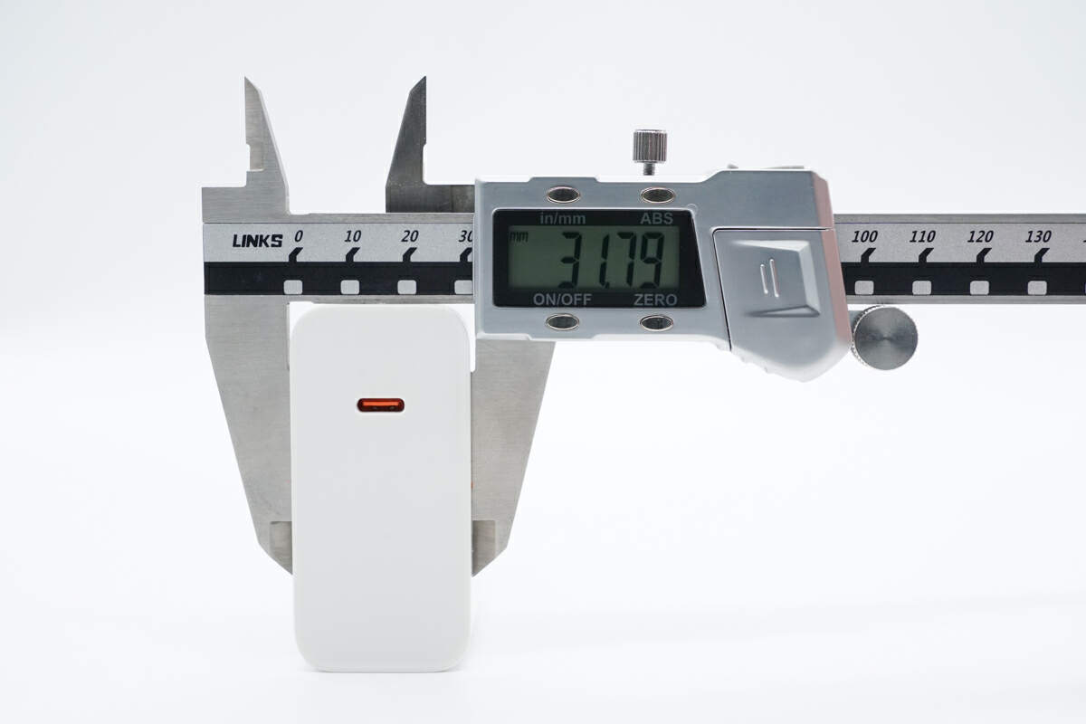
The thickness is about 32 mm (1.26 inches).

Teardown of Infinix 180W USB-C GaN Charger (U1800XEA)-Chargerlab

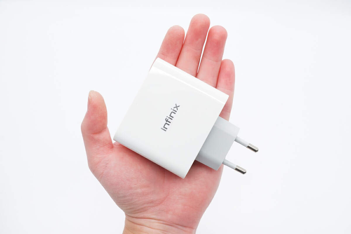
That's how big it is in the hand.

Teardown of Infinix 180W USB-C GaN Charger (U1800XEA)-Chargerlab

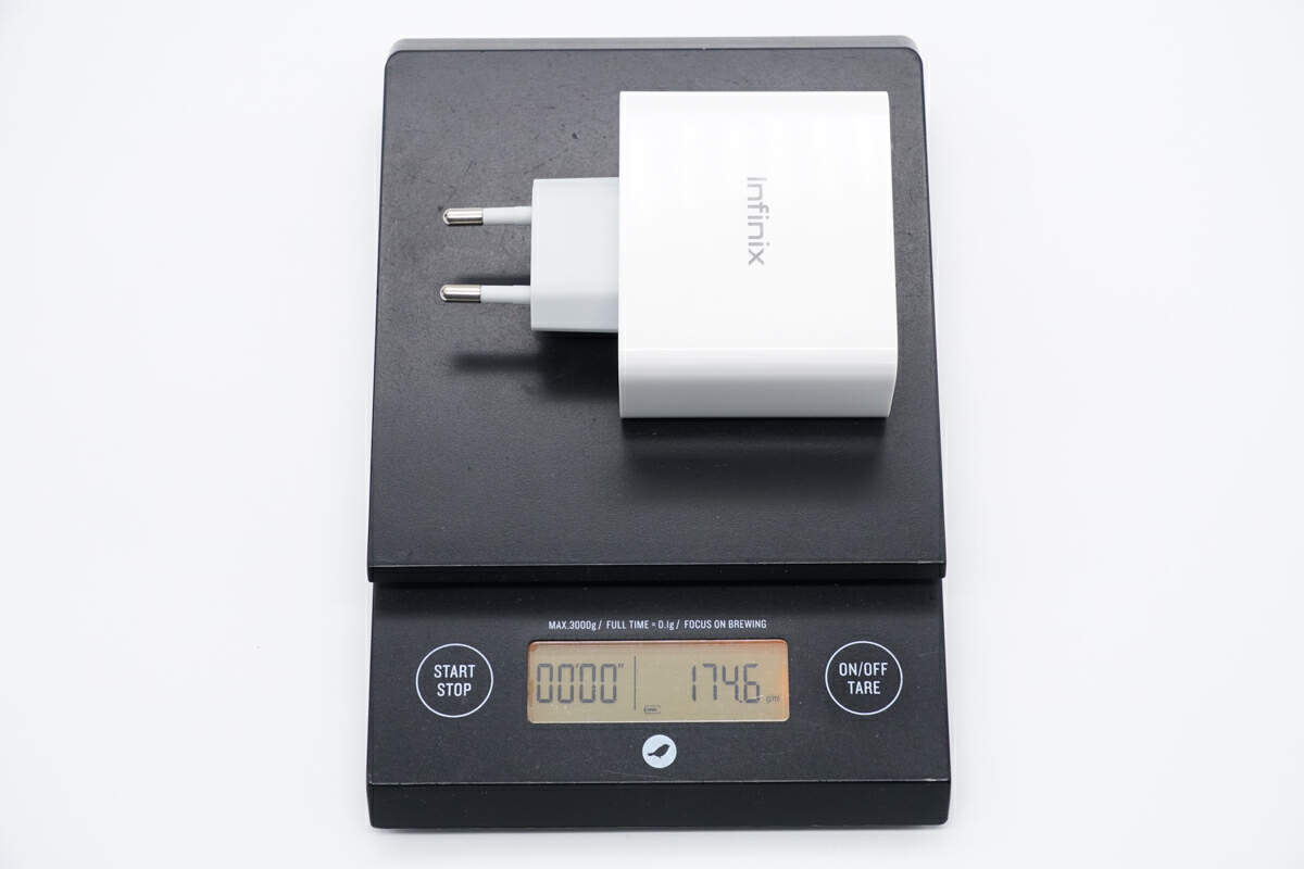
The weight is about 175 g (6.17 oz).

Teardown of Infinix 180W USB-C GaN Charger (U1800XEA)-Chargerlab

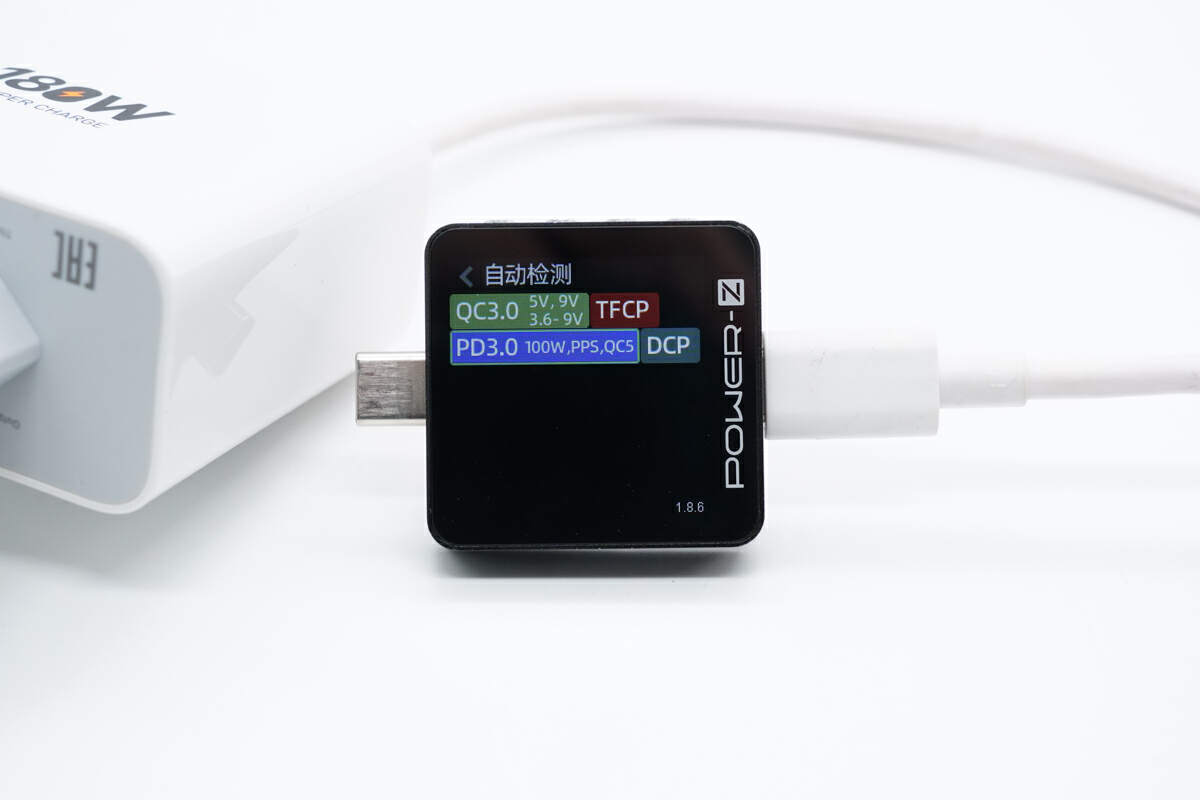
The ChargerLAB POWER-Z KM003C shows the USB-C port can support QC3.0, TFCP, PD3.0, PPS, QC5, and DCP charging protocols. 

Teardown of Infinix 180W USB-C GaN Charger (U1800XEA)-Chargerlab

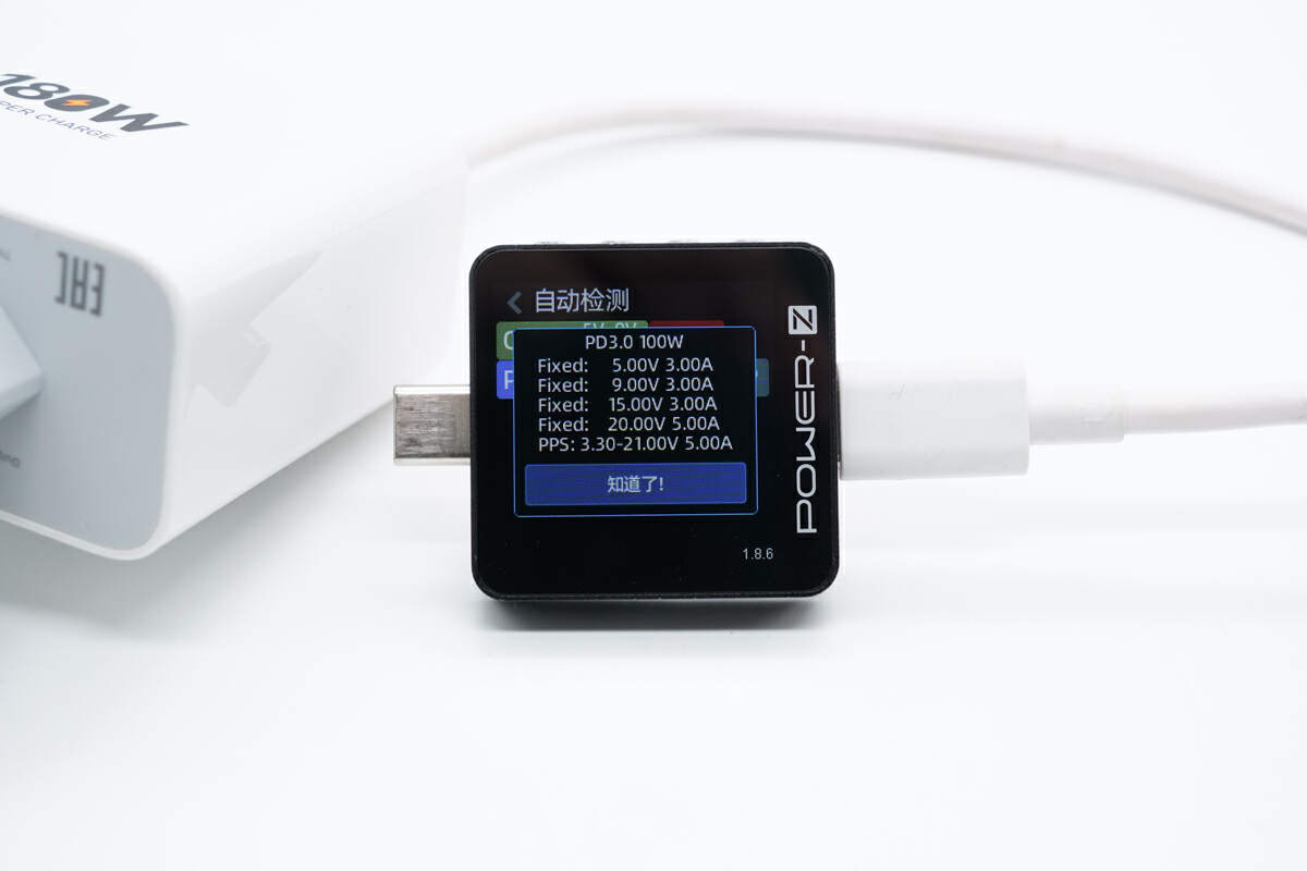
And it has four fixed PDOs of 5V3A, 9V3A, 15V3A, 20V5A, and a set of PPS, which is 3.3-21V5A.

Teardown

After the product's appearance, let's start to take it apart.

Teardown of Infinix 180W USB-C GaN Charger (U1800XEA)-Chargerlab

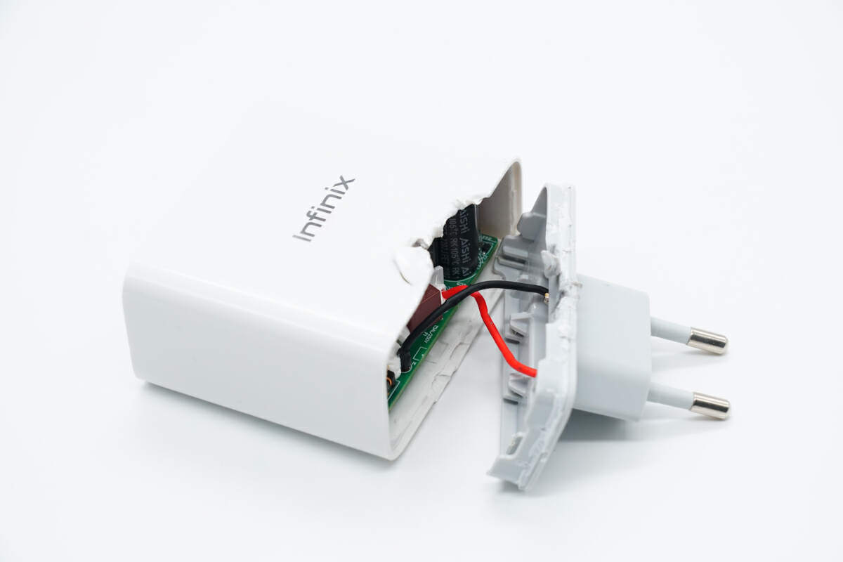
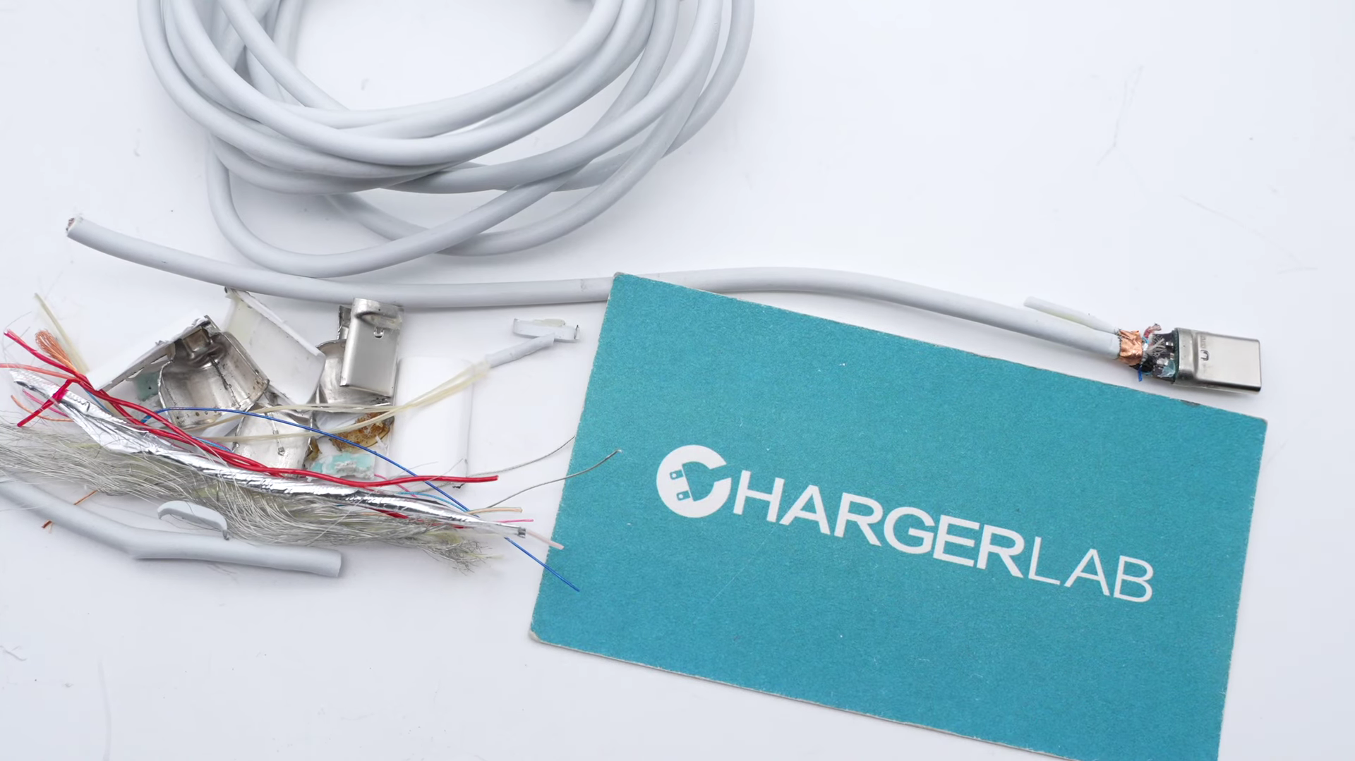
Remove the cover along the gap. The PCBA module and the prongs are connected by wires.

Teardown of Infinix 180W USB-C GaN Charger (U1800XEA)-Chargerlab

The wires are soldered to the PCBA module.

Teardown of Infinix 180W USB-C GaN Charger (U1800XEA)-Chargerlab

The foldable prongs are connected by crimping.

Teardown of Infinix 180W USB-C GaN Charger (U1800XEA)-Chargerlab

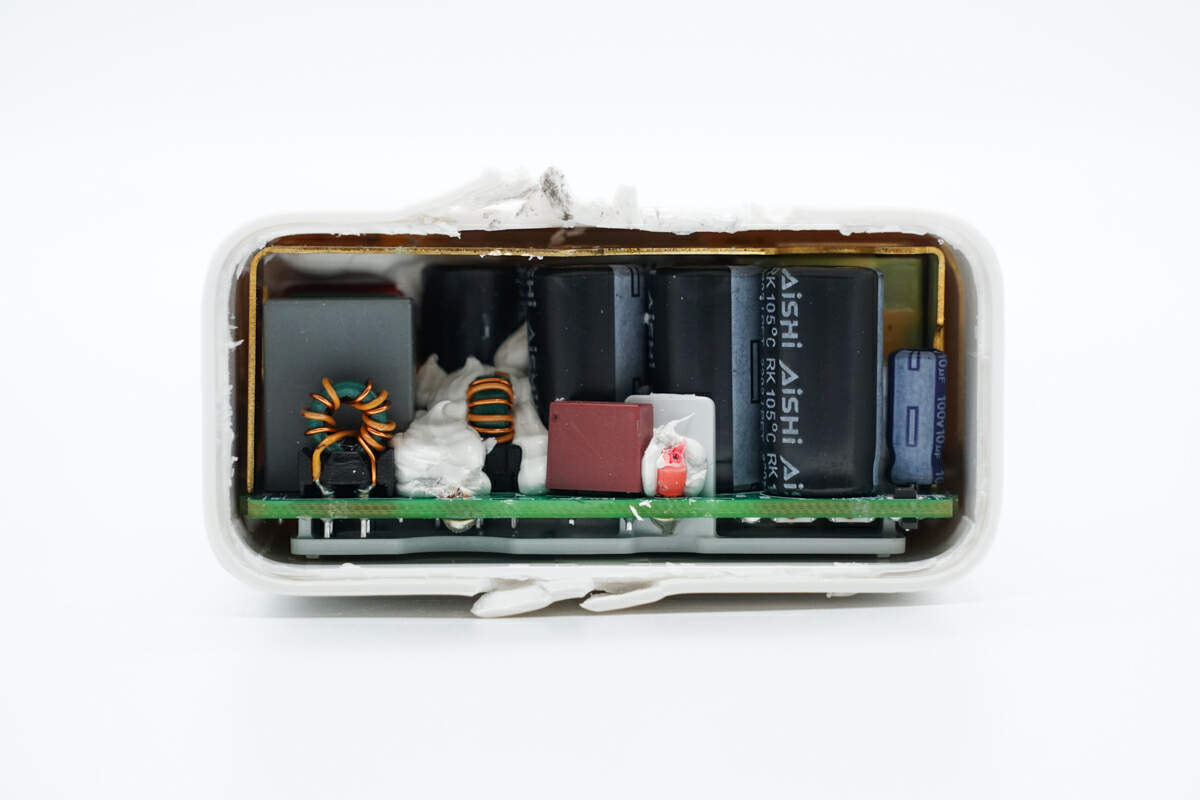
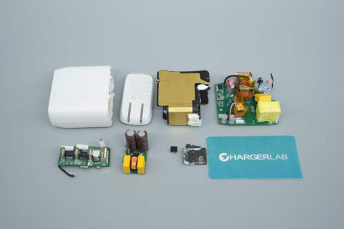
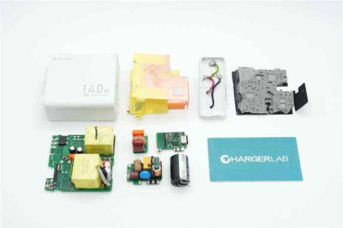
Here is the PCBA module.

Teardown of Infinix 180W USB-C GaN Charger (U1800XEA)-Chargerlab

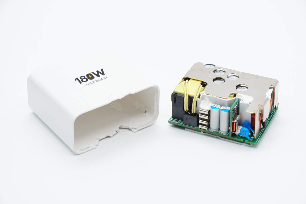
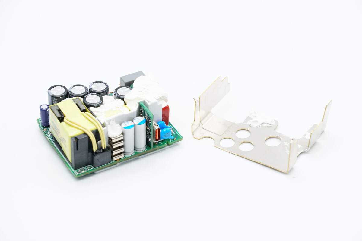
Take out the PCBA module from the case.

Teardown of Infinix 180W USB-C GaN Charger (U1800XEA)-Chargerlab

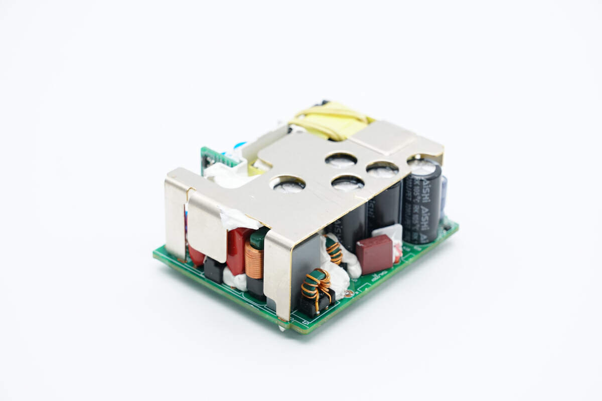
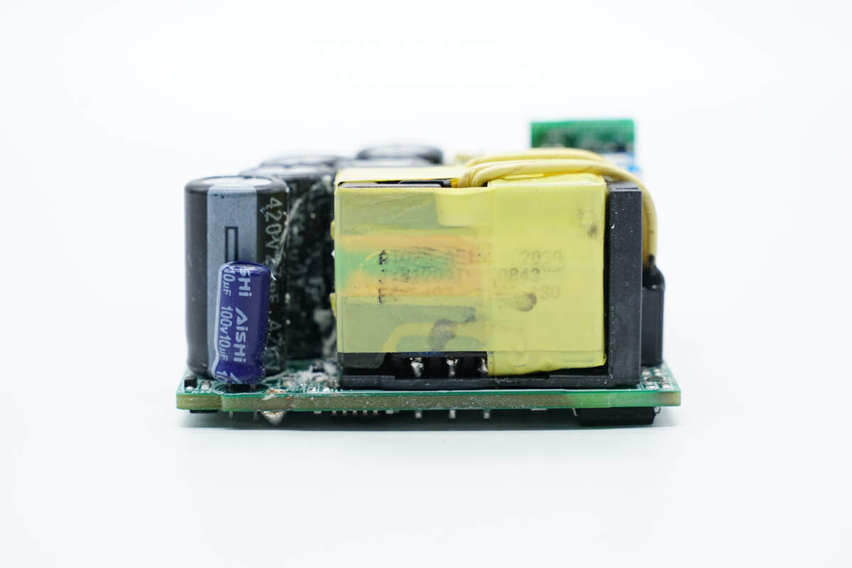
There is a heat sink on the top of the PCBA module.

Teardown of Infinix 180W USB-C GaN Charger (U1800XEA)-Chargerlab

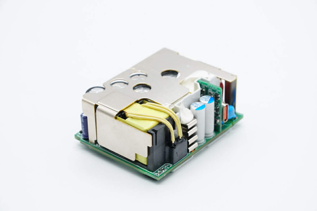
There is a white board between the primary and secondary sides for insulation.

Teardown of Infinix 180W USB-C GaN Charger (U1800XEA)-Chargerlab

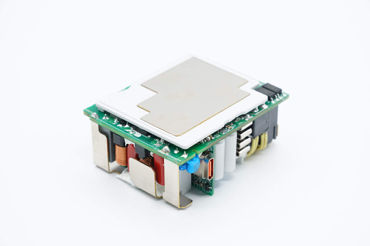
There is also a white plastic board on the back of the PCBA module for isolation. And there is a metal sheet on the board to enhance the heat dissipation.

Teardown of Infinix 180W USB-C GaN Charger (U1800XEA)-Chargerlab

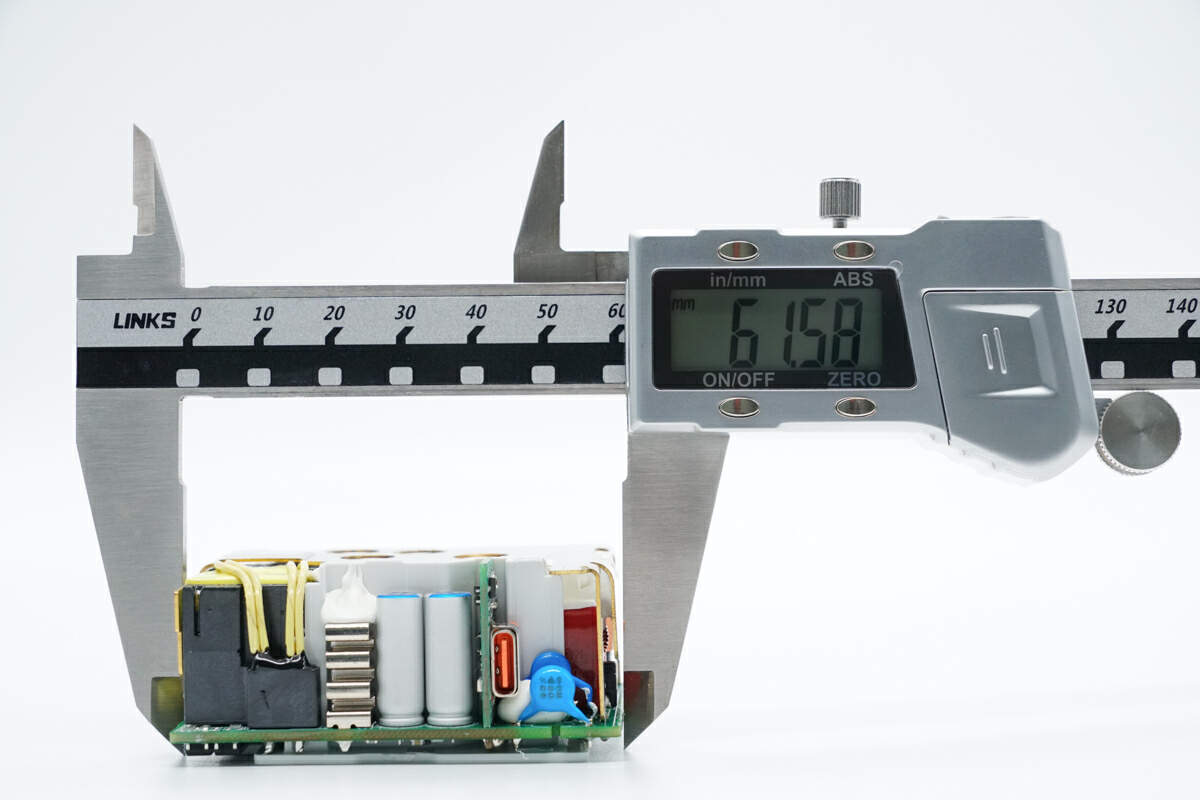
The length of the PCBA module is about 62 mm (2.44 inches).

Teardown of Infinix 180W USB-C GaN Charger (U1800XEA)-Chargerlab

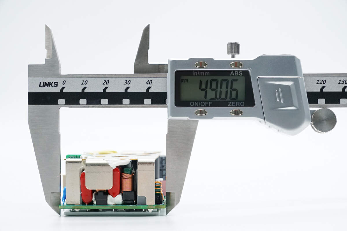
The width is about 49 mm (1.93 inches).

Teardown of Infinix 180W USB-C GaN Charger (U1800XEA)-Chargerlab

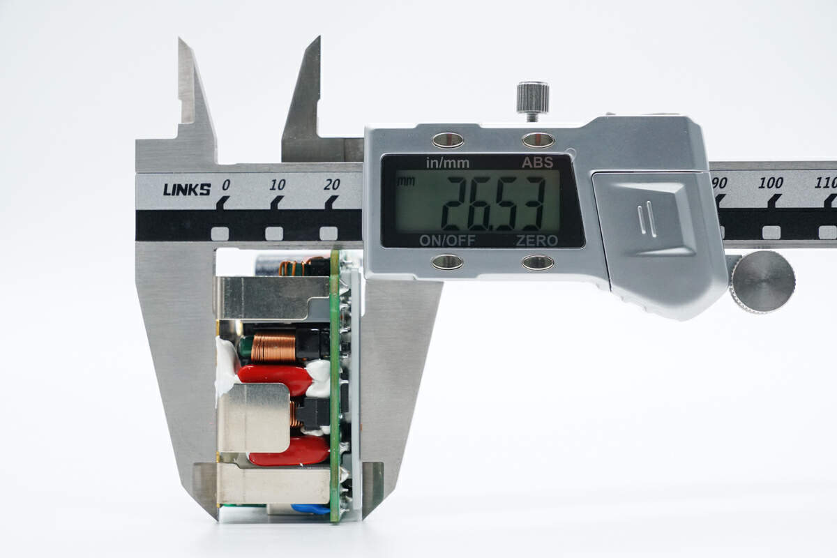
The thickness is about 27 mm (1.06 inches).

Teardown of Infinix 180W USB-C GaN Charger (U1800XEA)-Chargerlab

Remove the heat sink. The position corresponding to the PFC boost inductor has potting compound for heat dissipation.

Teardown of Infinix 180W USB-C GaN Charger (U1800XEA)-Chargerlab

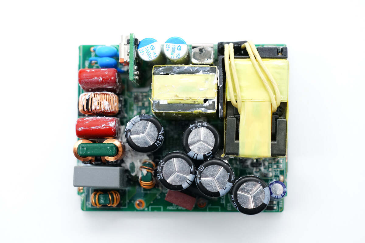
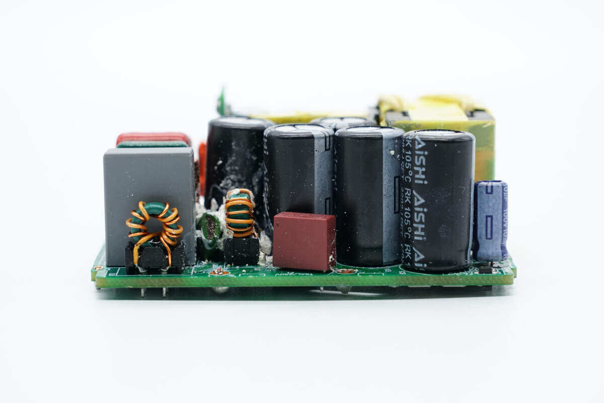
There are fuse, common mode choke, capacitors, inductors, small PCB of USB-C, and transformer on the front.

Teardown of Infinix 180W USB-C GaN Charger (U1800XEA)-Chargerlab

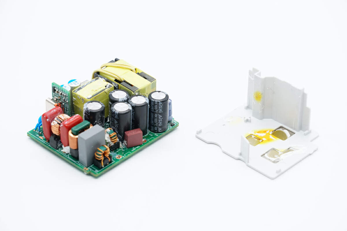
Remove the heat sink on the back of the PCBA module. The position corresponding to the GaN FET and rectifier has potting compound for heat dissipation.

Teardown of Infinix 180W USB-C GaN Charger (U1800XEA)-Chargerlab

The PFC controller, PFC rectifier, flyback controller, optocouplers, SMD Y capacitor, and synchronous rectifier controller are on the back.

ChargerLAB found it adopts a PFC circuit and flyback topology with synchronous rectification.

Next, we will take a look at each component starting from the input end.

Teardown of Infinix 180W USB-C GaN Charger (U1800XEA)-Chargerlab

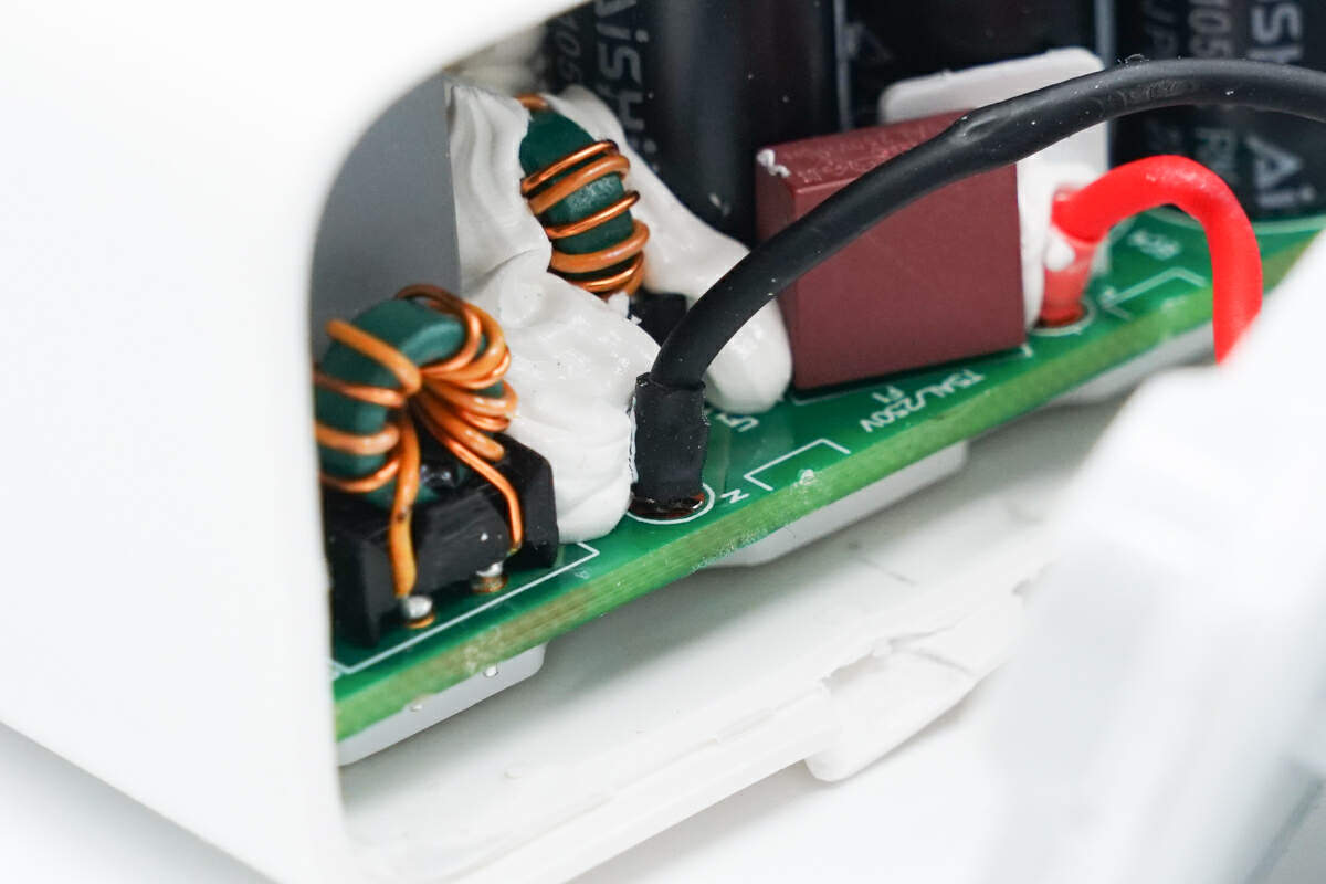
There are fuse, common mode choke, and safety X2 capacitor at the input end.

Teardown of Infinix 180W USB-C GaN Charger (U1800XEA)-Chargerlab

The input fuse marked with 932 is from Betterfuse. 5A 250V.

Teardown of Infinix 180W USB-C GaN Charger (U1800XEA)-Chargerlab

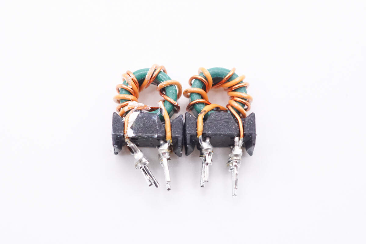
The common mode chokes are wound with magnets and insulated wires, and they're also insulated with frames.

Teardown of Infinix 180W USB-C GaN Charger (U1800XEA)-Chargerlab

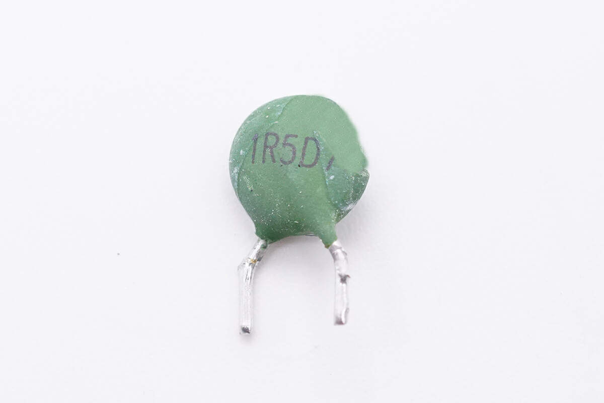
The green thermistor is used to suppress the surge current.

Teardown of Infinix 180W USB-C GaN Charger (U1800XEA)-Chargerlab

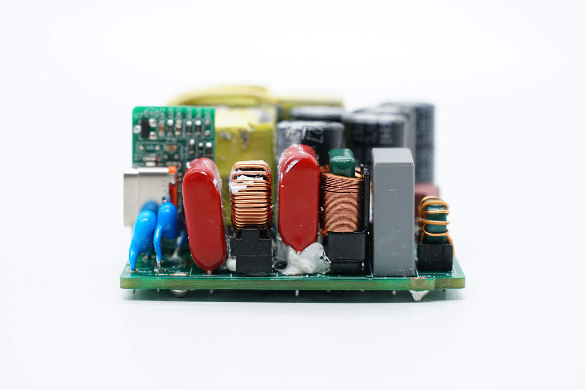
There are common mode choke, safety X2 capacitor, film filter capacitors, and blue Y capacitors on the side of the PCBA module.

Teardown of Infinix 180W USB-C GaN Charger (U1800XEA)-Chargerlab

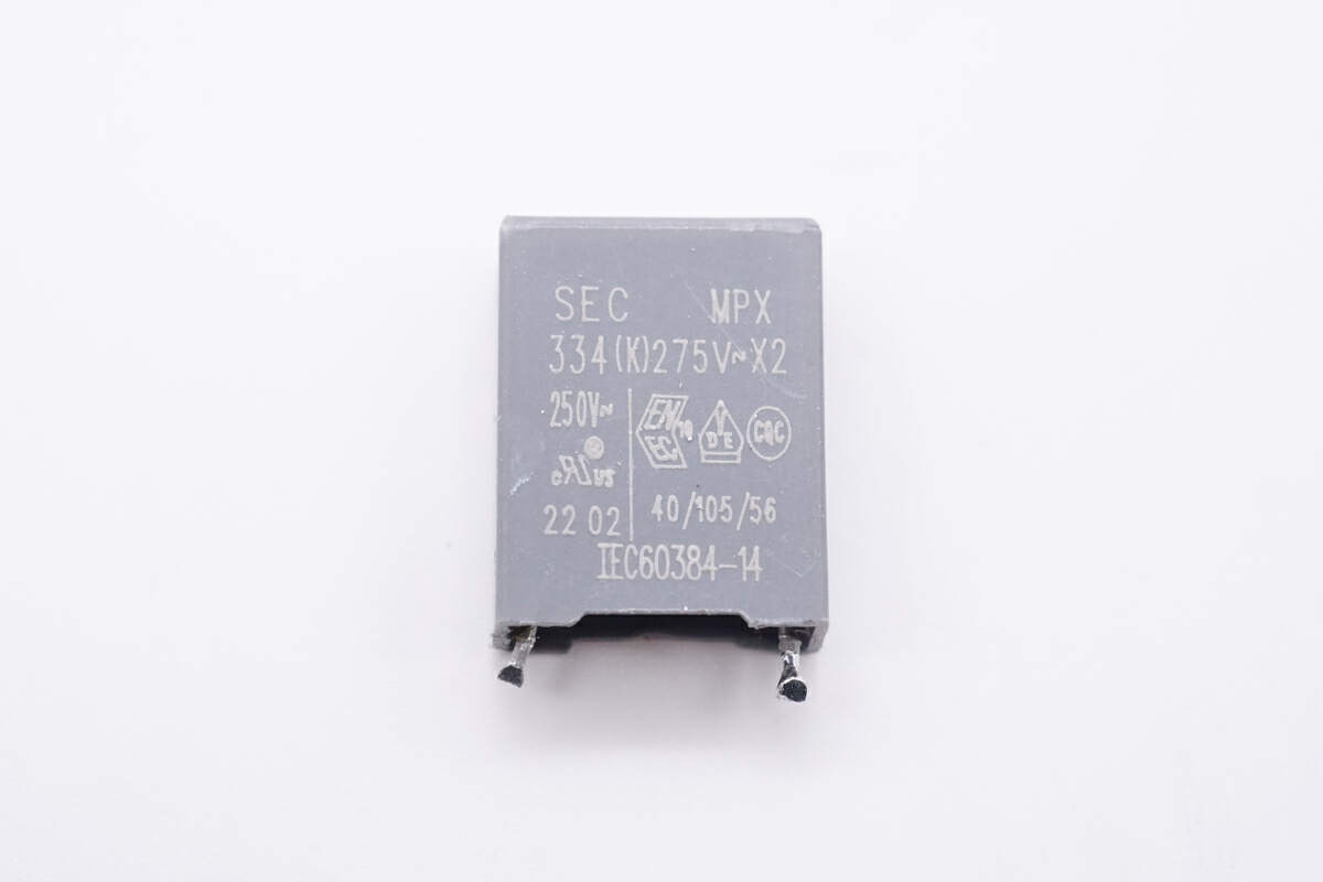
The safety X2 capacitor is from SEC. 0.33μF.

Teardown of Infinix 180W USB-C GaN Charger (U1800XEA)-Chargerlab

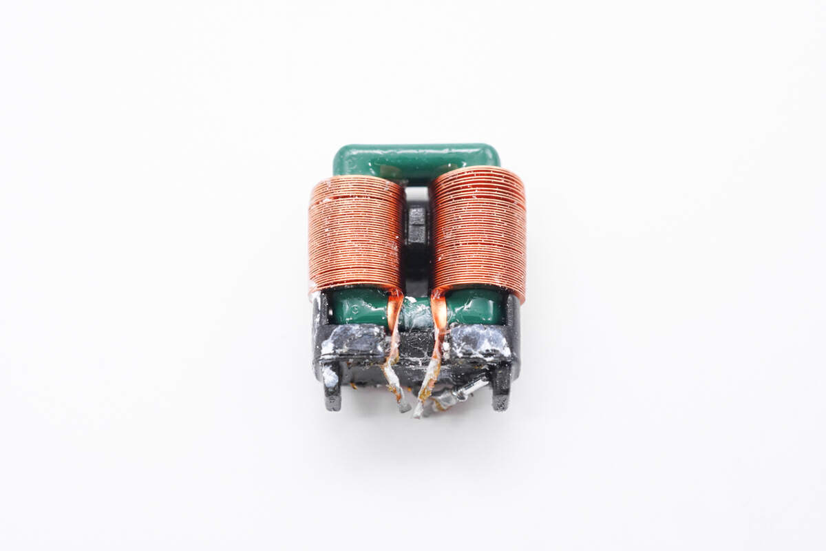
Another common mode choke is wound with flat copper wire, and insulated with a frame.

Teardown of Infinix 180W USB-C GaN Charger (U1800XEA)-Chargerlab

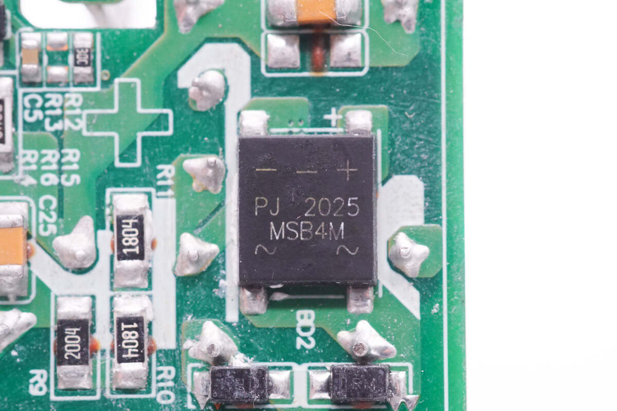
The bridge rectifier is from PANJIT. Model is MSB4M. 1000V 4A.

Teardown of Infinix 180W USB-C GaN Charger (U1800XEA)-Chargerlab

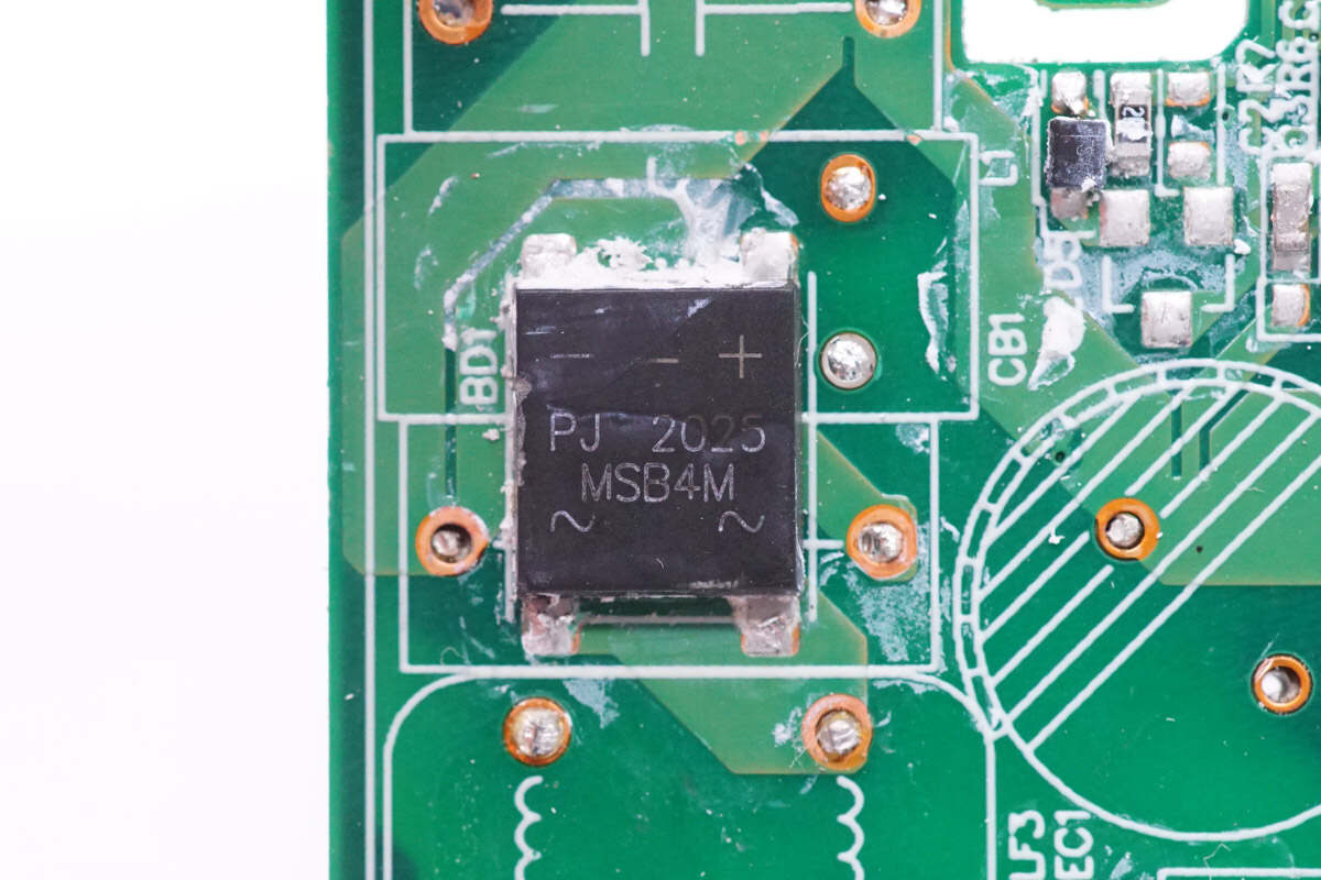
The other bridge rectifier is the same as the previous one. The two bridge rectifiers can share the heat equally.

Teardown of Infinix 180W USB-C GaN Charger (U1800XEA)-Chargerlab

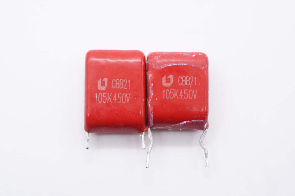
There are two film filter capacitors. 1μF 450V.

Teardown of Infinix 180W USB-C GaN Charger (U1800XEA)-Chargerlab

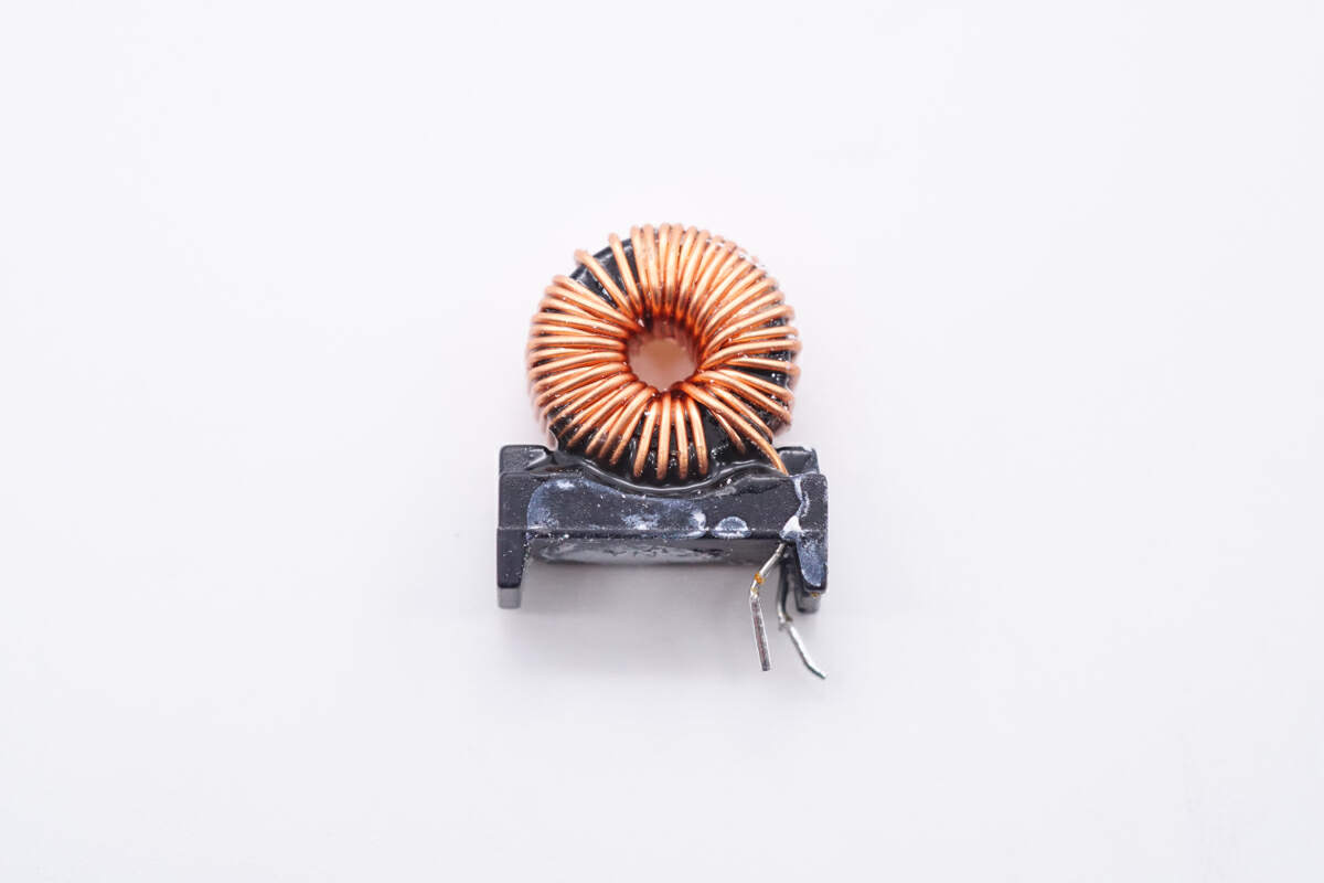
The filter inductor is wounded with magnetic ring and insulated by a black frame.

Teardown of Infinix 180W USB-C GaN Charger (U1800XEA)-Chargerlab

The PFC controller is from Silergy. It integrates the boost converter for high efficiency. Model is SY5072B. 

Teardown of Infinix 180W USB-C GaN Charger (U1800XEA)-Chargerlab

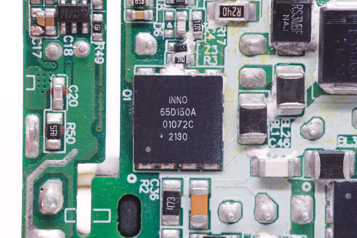
The PFC boost MOSFET is from Innoscience and adopts DFN8 x 8 package. It supports high switching frequency and has the low gate charge and output charge. Model is INN650D150A. 650V 150mΩ.

Teardown of Infinix 180W USB-C GaN Charger (U1800XEA)-Chargerlab

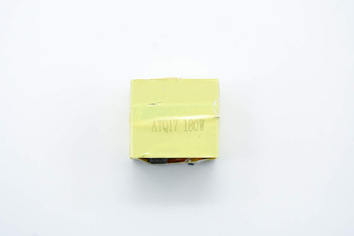
The PFC boost inductor is wound with ATQ17 magnetic core. 180W.

Teardown of Infinix 180W USB-C GaN Charger (U1800XEA)-Chargerlab

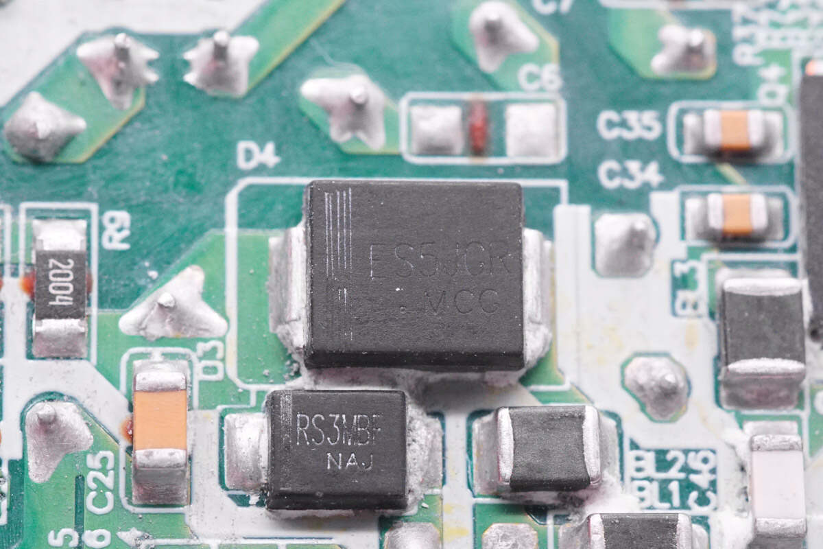
The PFC rectifier is from Pingwei. Model is ES5JGR. 5A 600V.

Teardown of Infinix 180W USB-C GaN Charger (U1800XEA)-Chargerlab

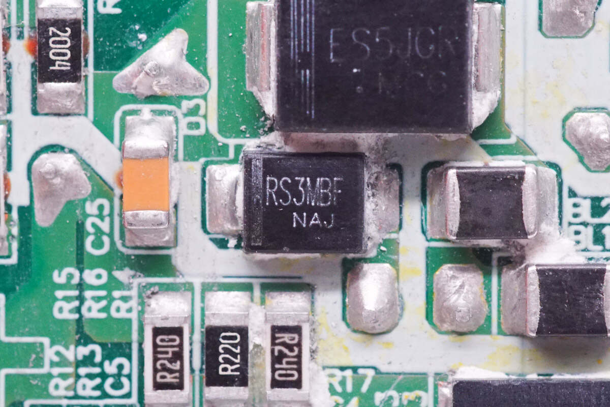
The diode is marked with RS3MBF.

Teardown of Infinix 180W USB-C GaN Charger (U1800XEA)-Chargerlab

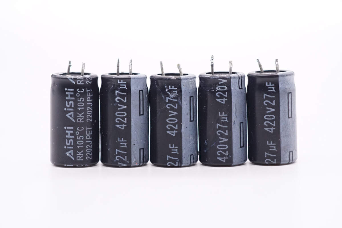
These electrolytic capacitors for input filtering are from AiSHi RK series and they are connected in in parallel. 420V 27μF for each. The total capacity is 135μF.

Teardown of Infinix 180W USB-C GaN Charger (U1800XEA)-Chargerlab

The PWM controller is from Dialog. It is a digital flyback controller that supports zero-voltage switching and adaptive multi-mode control operation. Model is iW9801. 

Teardown of Infinix 180W USB-C GaN Charger (U1800XEA)-Chargerlab

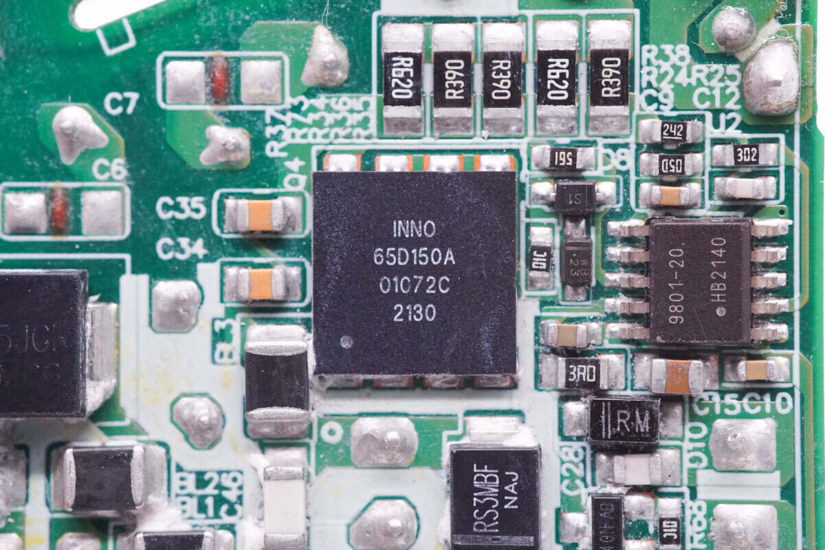
This MOSFET is from Innoscience. Model is INN650D150A. 

Teardown of Infinix 180W USB-C GaN Charger (U1800XEA)-Chargerlab

There are filter capacitors and a transformer on the side of the PCBA module.

Teardown of Infinix 180W USB-C GaN Charger (U1800XEA)-Chargerlab

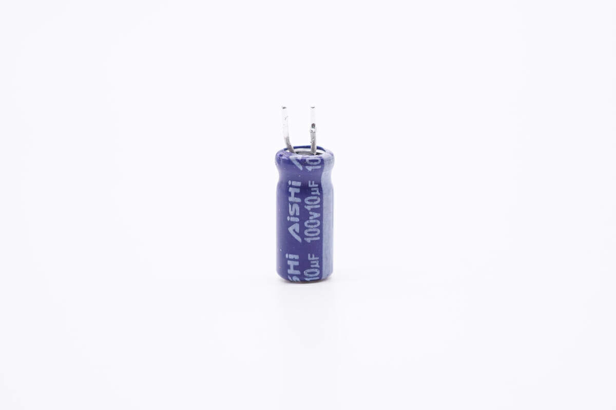
This is the filter capacitor that powers the master control chip. 100V 10μF. 

Teardown of Infinix 180W USB-C GaN Charger (U1800XEA)-Chargerlab

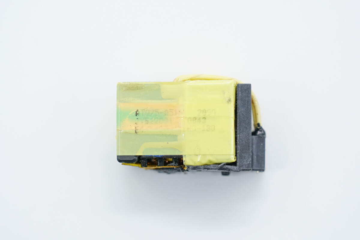
The transformer adopts ATQ25 magnetic core.

Teardown of Infinix 180W USB-C GaN Charger (U1800XEA)-Chargerlab

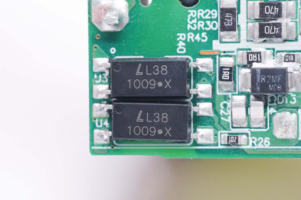
These two optocouplers are used for PFC control and output voltage feedback respectively.

Teardown of Infinix 180W USB-C GaN Charger (U1800XEA)-Chargerlab

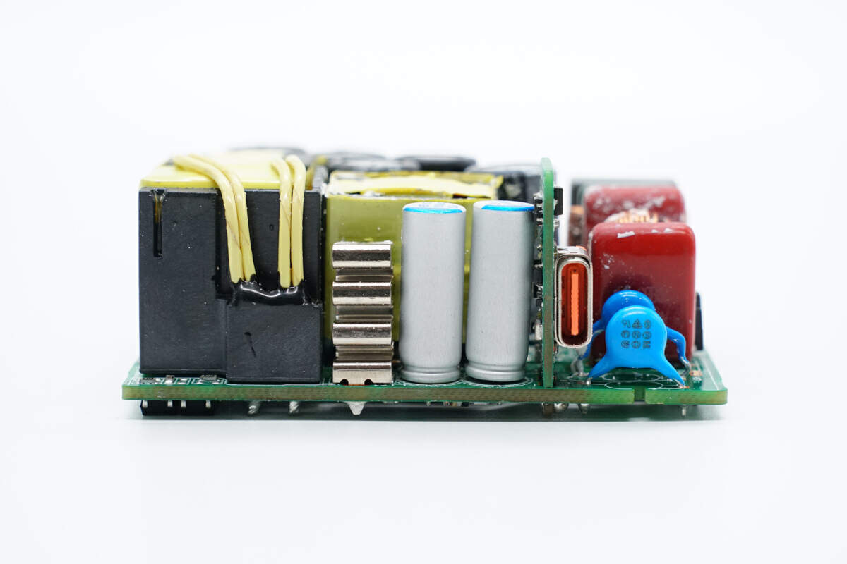
The output side has a synchronous rectifier, two solid capacitors, a PCB of USB-C socket, and two blue Y capacitors.

Teardown of Infinix 180W USB-C GaN Charger (U1800XEA)-Chargerlab

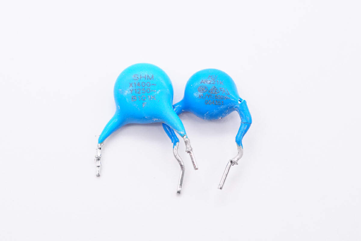
There are two blue Y capacitors.

Teardown of Infinix 180W USB-C GaN Charger (U1800XEA)-Chargerlab

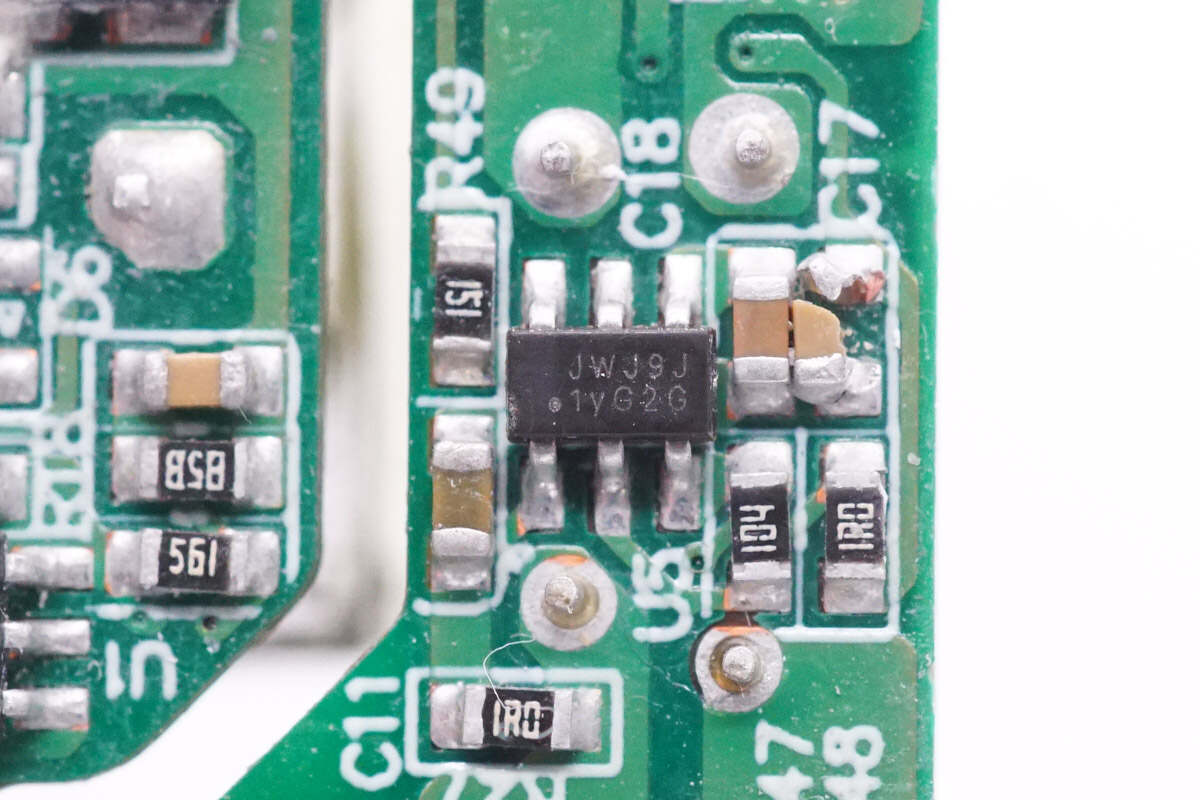
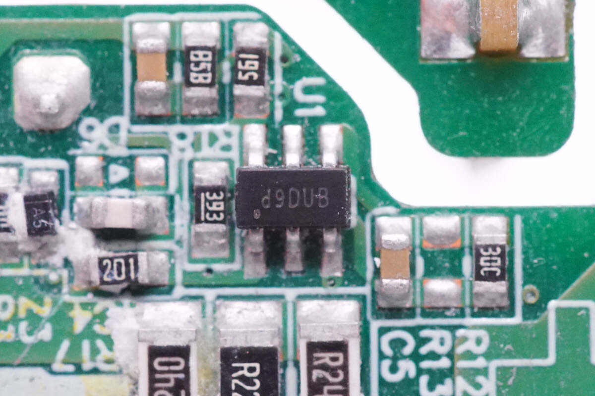
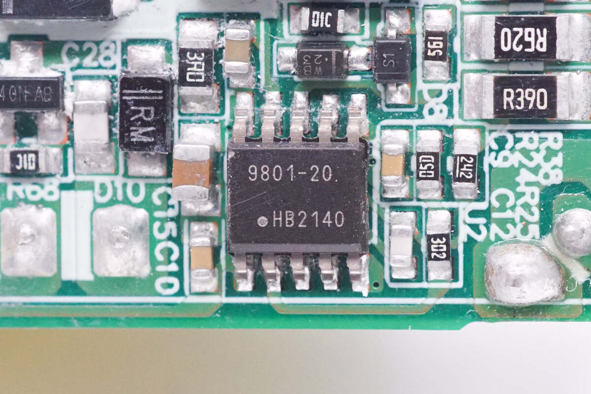
The synchronous rectifier controller marked with JWJ9J is from JOULWATT. It supports modes of DCM, CCM, QR, and ACF. Model is JW7726B. 

Teardown of Infinix 180W USB-C GaN Charger (U1800XEA)-Chargerlab

There is all the information about the JOULWATT JW7726B. 

Teardown of Infinix 180W USB-C GaN Charger (U1800XEA)-Chargerlab

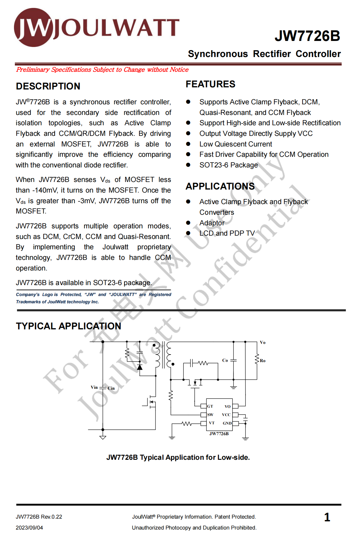
The synchronous rectifier is from AOS and adopts DFN5 x 6 package. Model is AONS66947. 100V 2.9mΩ. 

Teardown of Infinix 180W USB-C GaN Charger (U1800XEA)-Chargerlab

This is the heat sink for the synchronous rectifier.

Teardown of Infinix 180W USB-C GaN Charger (U1800XEA)-Chargerlab

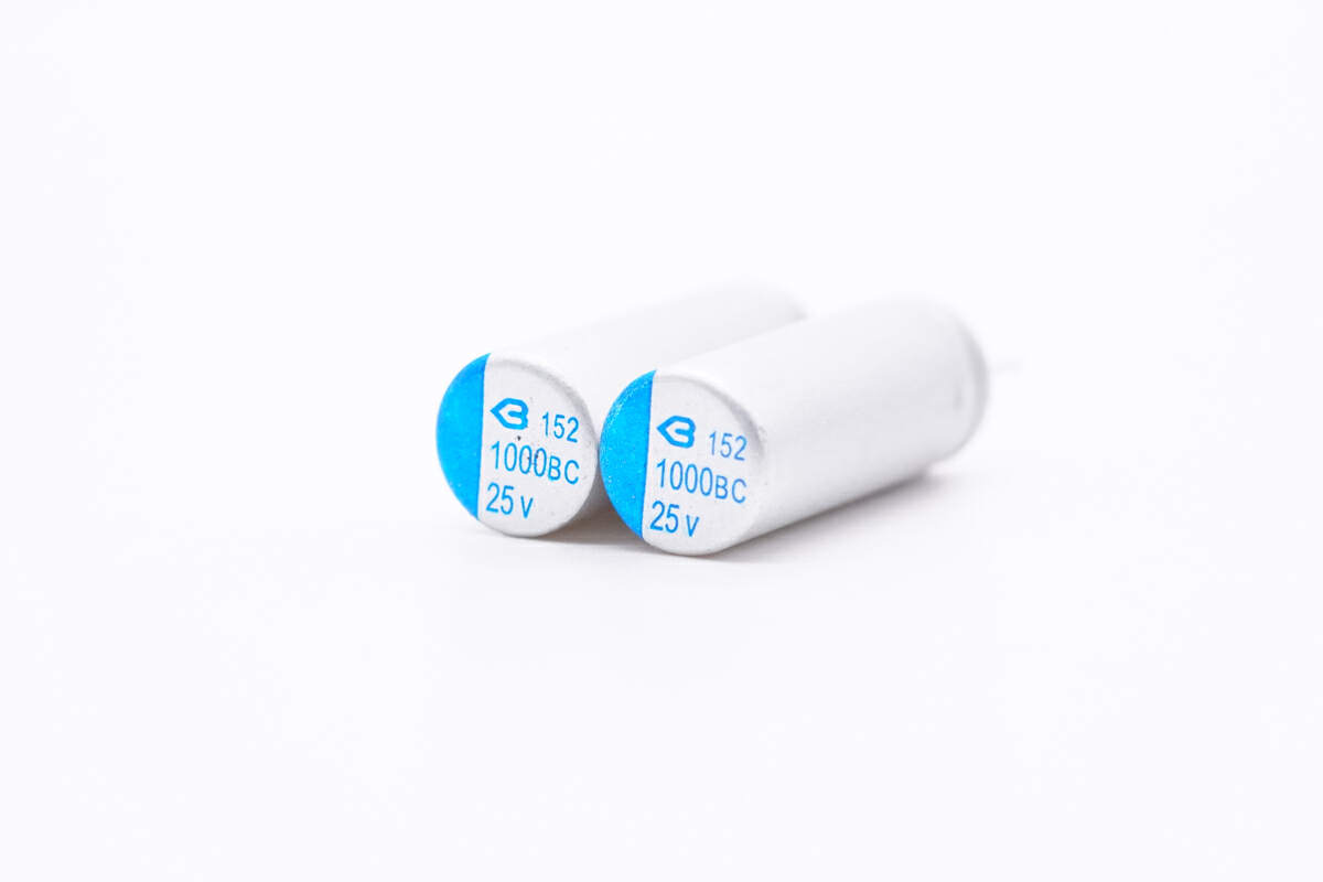
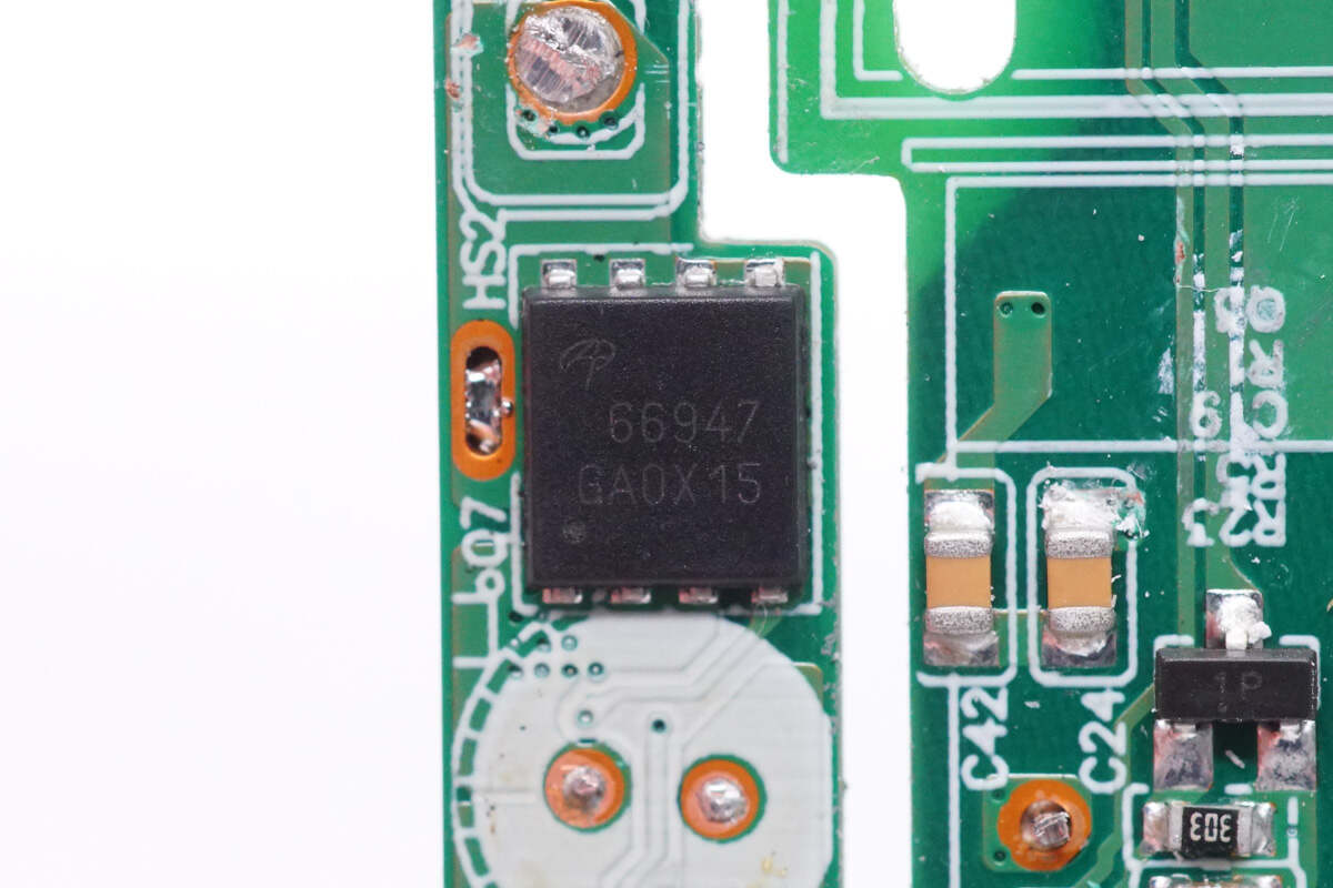
These two solid capacitors are from BERYL. 1000μF 25V, respectively. 

Teardown of Infinix 180W USB-C GaN Charger (U1800XEA)-Chargerlab

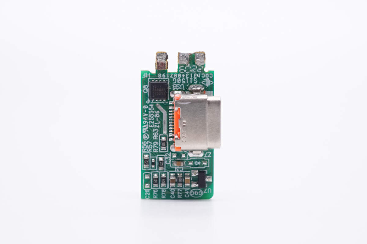
There is a VBUS MOSFET on the front of the PCB of the USB-C socket. 

Teardown of Infinix 180W USB-C GaN Charger (U1800XEA)-Chargerlab

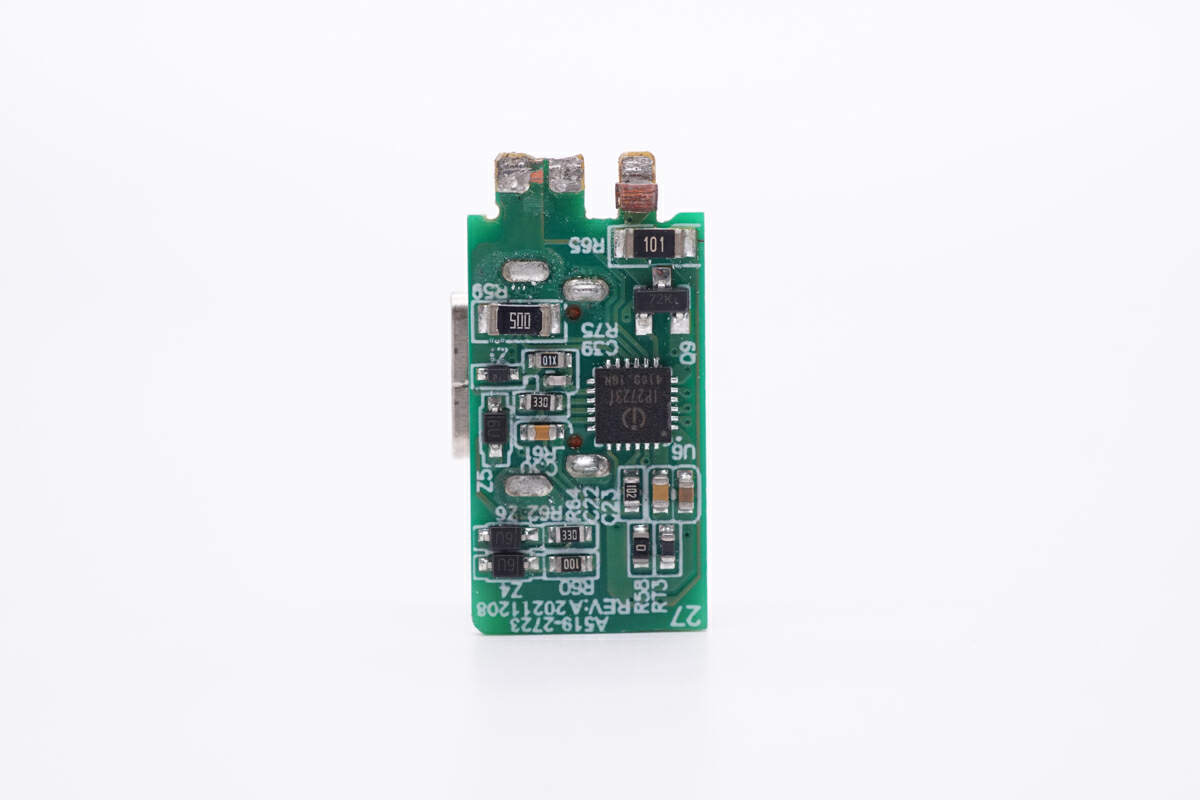
The protocol chip, current sampling resistor, TVS diode, and thermistor are on the back.

Teardown of Infinix 180W USB-C GaN Charger (U1800XEA)-Chargerlab

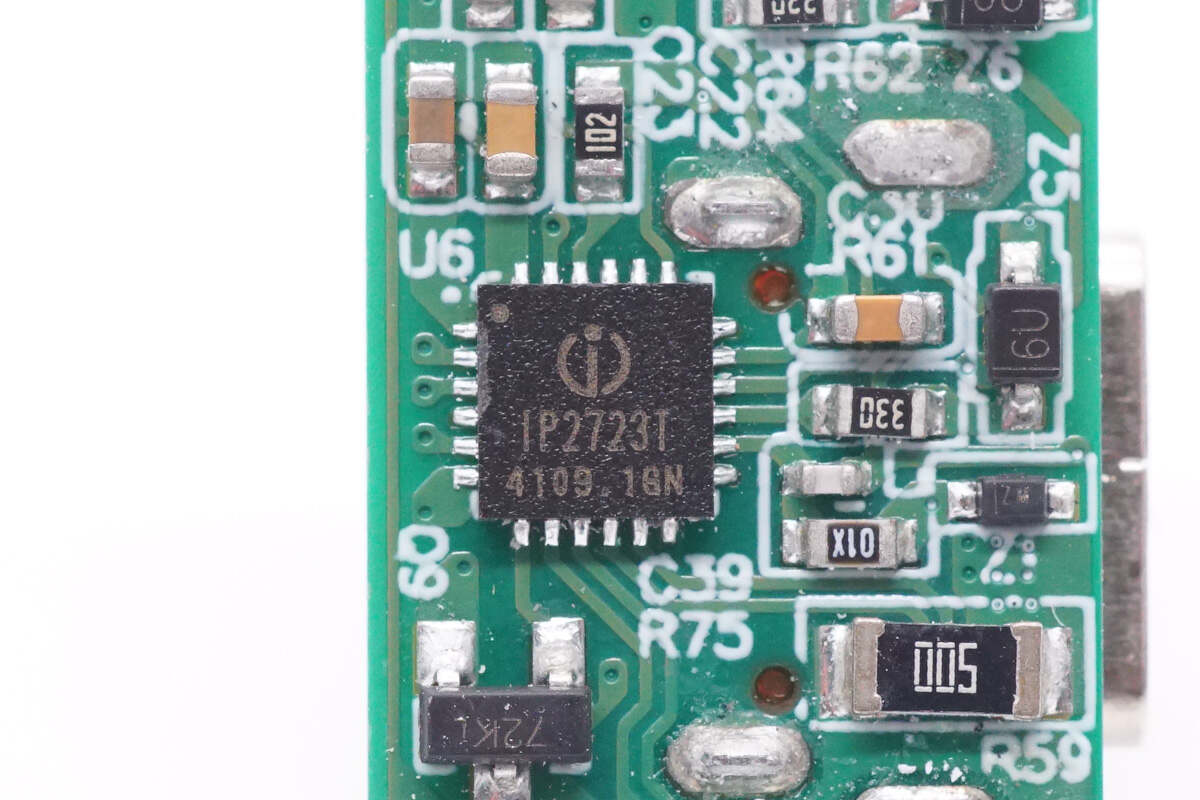
The protocol chip is from Injoinic. It supports a variety of fast charging protocols, including DFP, PD2.0/3.0, PPS, QC4, QC4+, QC3.0/2.0, FCP, SCP, AFC, MTK PE+ 2.0/1.1, Apple 2.4A, and SAM 2A. Model is IP2723T. 

Teardown of Infinix 180W USB-C GaN Charger (U1800XEA)-Chargerlab

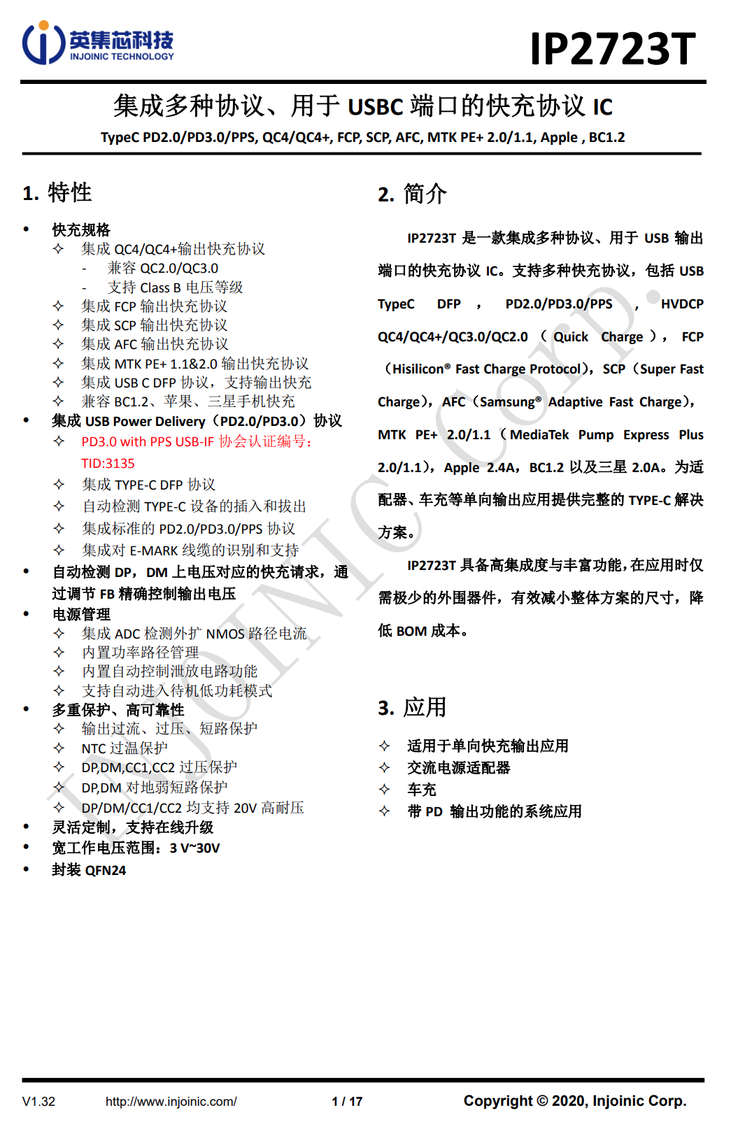
There is all the information of the Injoinic IP2723T. 

Teardown of Infinix 180W USB-C GaN Charger (U1800XEA)-Chargerlab

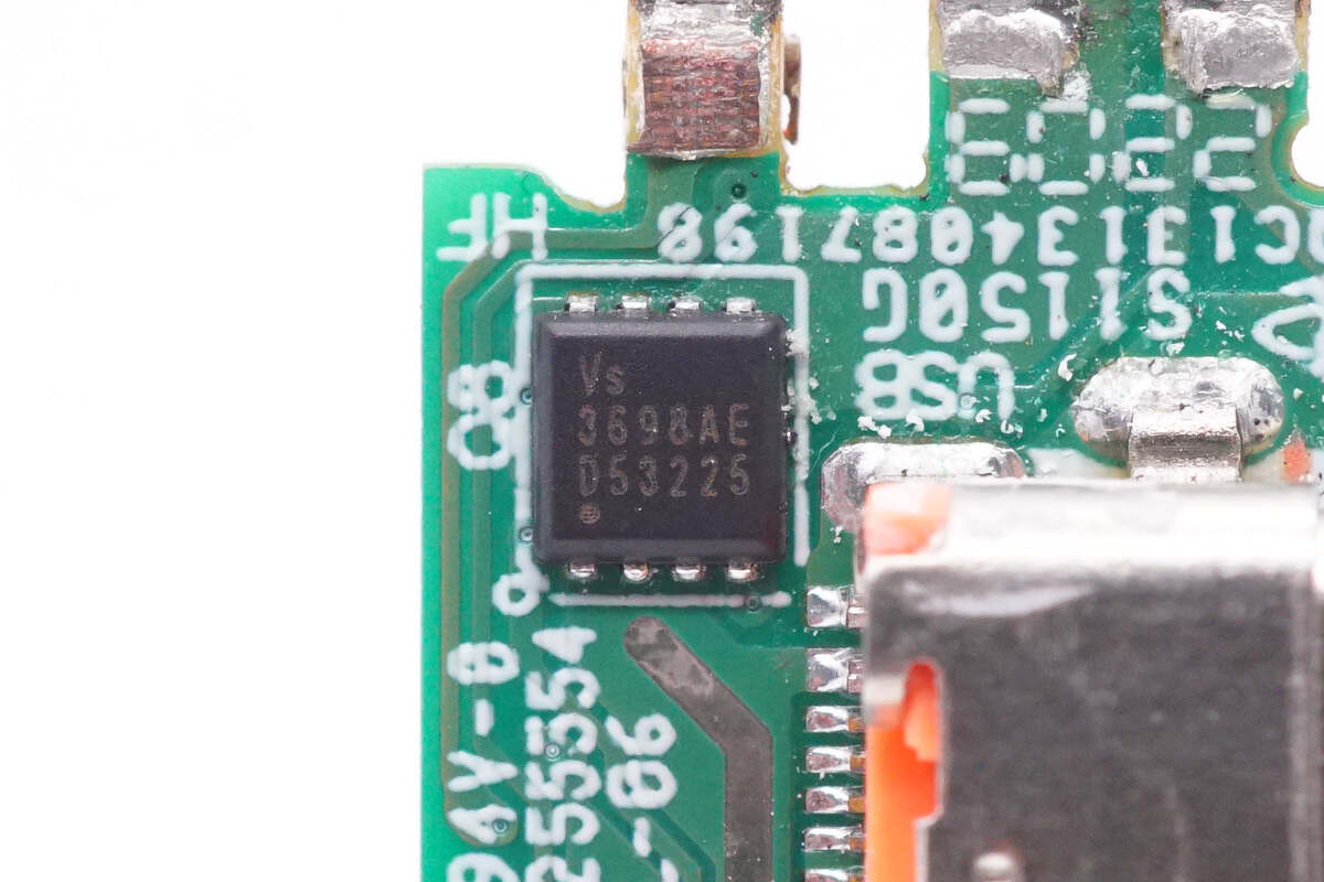
The VBUS MOSFET for output is from VGSEMI and adopts PDFN3333 package. Model is VS3698AE. 30V 3mΩ. 

Teardown of Infinix 180W USB-C GaN Charger (U1800XEA)-Chargerlab

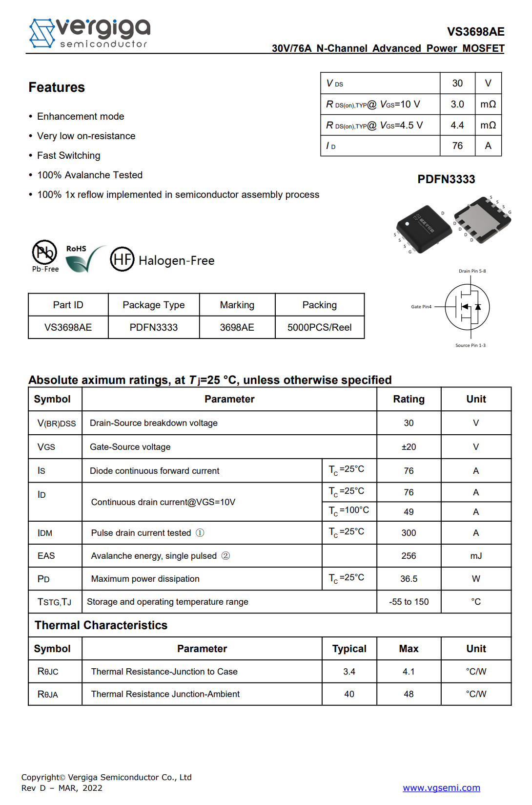
There is all the information about the VGSEMI VS3698AE.

Teardown of Infinix 180W USB-C GaN Charger (U1800XEA)-Chargerlab

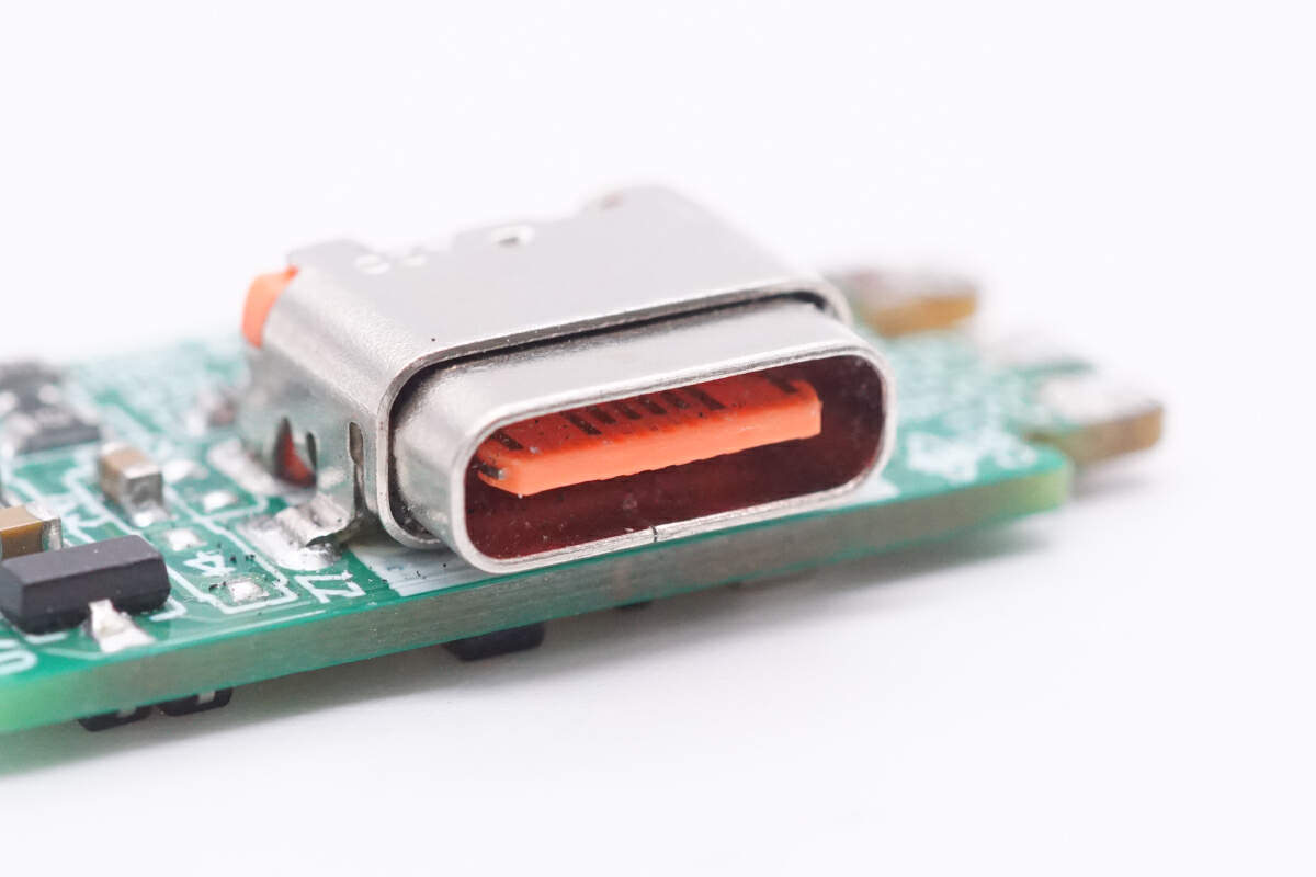
There is the orange USB-C socket.

Teardown of Infinix 180W USB-C GaN Charger (U1800XEA)-Chargerlab

Well, those are all components of the Infinix 180W USB-C GaN charger.

Summary of ChargerLAB

It adopts a one-piece white case and European pins. The maximum output power is 20V9A 180W. It can also support fast charging of 100W PD and 3.3-21V5A PPS. It has good fast charging compatibility for Android phones and laptops.

After taking it apart, we found it adopts a PFC circuit and flyback topology. It uses a PFC controller and a ZVS flyback controller, paired with two GaN FETs. The charger has copper heat sinks to dissipate heat for the PFC boost inductor and GaN FETs. The internal components are fixed with glue, and the workmanship is solid. 

Related Articles:
1. PD3.1 | Teardown of Kovol 140W GaN Charger
2. Teardown of MOVESPEED 140W PD3.1 4-in-1 Charger (YSFCG107-140Y)
3. Teardown of LDNIO 140W GaN 6-in-1 Desktop Charger (A6140C)

180W Infinix
1
myCharge Recalls POWER HUB ALL-In-One Portable Chargers Due to Fire and Burn Hazards;Sold Exclusively at Costco
Previous
EcoFlow Launches New DELTA Pro 3 Series with X-CORE 3.0 Technology for a Revolutionary Experience
Next

Hot posts

Anker Prime Thunderbolt 5 Docking Station: 14 Ports, Dual 8K Support, and 140W Power Delivery
Charging Compatibility Test of Nintendo Switch 2 (Handheld Mode)
Teardown of vivo 90W FlashCharge GaN Charger
Teardown of Xiaomi 15S Pro 15th Anniversary Edition: Featuring 3nm Self-Developed SoC Xring O1

Related posts

Teardown of Dell 130W USB-C Power Adapter (HA130PM170)

Teardown of Dell 130W USB-C Power Adapter (HA130PM170)

September 2, 2021
4
AUKEY PA-Y19 27W PD Charger Teardown Review: GaNFast Inside

AUKEY PA-Y19 27W PD Charger Teardown Review: GaNFast Inside

May 21, 2019
0
Teardown of Xiaomi 80W Wireless Charging Stand (White)

Teardown of Xiaomi 80W Wireless Charging Stand (White)

October 15, 2021
0
Teardown of ASUS ROG 130W USB-C GaN Power Adapter (ADP-130HB B)

Teardown of ASUS ROG 130W USB-C GaN Power Adapter (ADP-130HB B)

November 11, 2024
1
1

ABOUT ME

As a sibling site of chongdiantou.com, ChargerLAB covers everything about charging, including chargers, wireless chargers, power banks, cables, car chargers, portable power stations and other peripherals. You can contact us by sending the email to info@chargerlab.com.

FOLLOW US

Facebook Instagram TikTok Twitter YouTube

E-COOL MEDIA

POWER-Z Chongdiantou 52Audio
Copyright © 2016-2025 Chargerlab. Designed by nicetheme.
  • News
    • What's New
    • Interviews
    • Vlogs
    • Events
    • Industry
  • Reviews
    • Charging Compatibility
    • Fully Charging
    • Comparison
    • Chargers & Cables
    • Power Banks & Stations
    • Mobile Devices
    • Accessories
  • Teardowns
    • Chargers & Cables
    • Power Banks & Stations
    • Power Supplies
    • Prototypes
    • Batteries
    • Accessories
  • Videos
    • YouTube
    • TikTok
  • Guides
    • How to Buy
    • Explained
    • Deals
    • ICs
  • POWER-Z
    • KM003C/KM002C
    • KT002
    • Buy POWER-Z
    • Technical Support
  • Contact Us
  • Apple
  • GaN
  • Power Bank
  • ANKER
  • 65W
  • iPhone 15
  • Qi2
  • ChargerLAB
  • USB-C
  • 100W

Rusell

Editor