Introduction
On November 25, Huawei officially released the Mate 80 series, which comes bundled with a very compact 66W charger. In addition to supporting Huawei’s 66W SuperCharge, it also supports 65W PD/PPS, allowing it to charge laptops, tablets, and other devices, including those from third-party brands. Below, we take a closer look at the detailed design and internal components of this charger.
Product Appearance
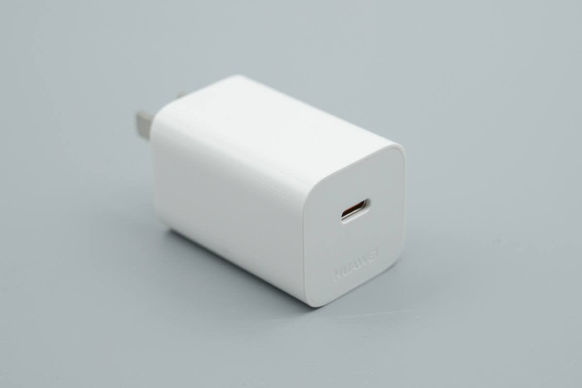
The enclosure is made of flame-retardant PC material with a glossy surface finish.
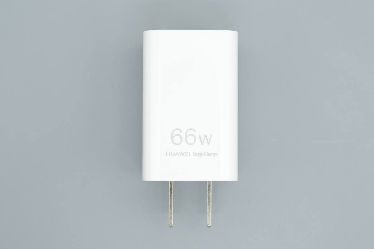
This side is printed with “66W” and “HUAWEI SuperCharge”.
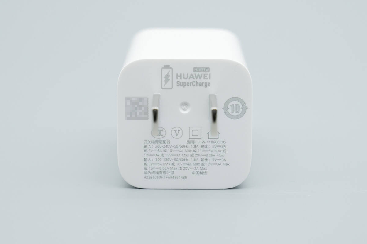
The charger specifications are printed on the input-side housing.
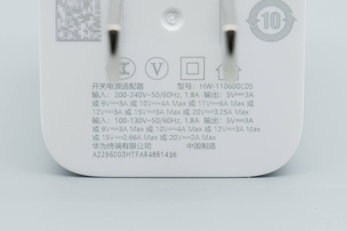
Model: HW-110600C05
Input: 200–240V~ 50/60Hz 1.8A
Output: 5V 3A, 9V 3A, 10V 4A, 11V 6A, 12V 3A, 15V 3A, 20V 3.25A Max
Input: 100–130V~ 50/60Hz 1.8A
Output: 5V 3A, 9V 3A, 10V 4A, 12V 3A, 15V 2.66A, 20V 2A Max
The charger has passed CCC certification.
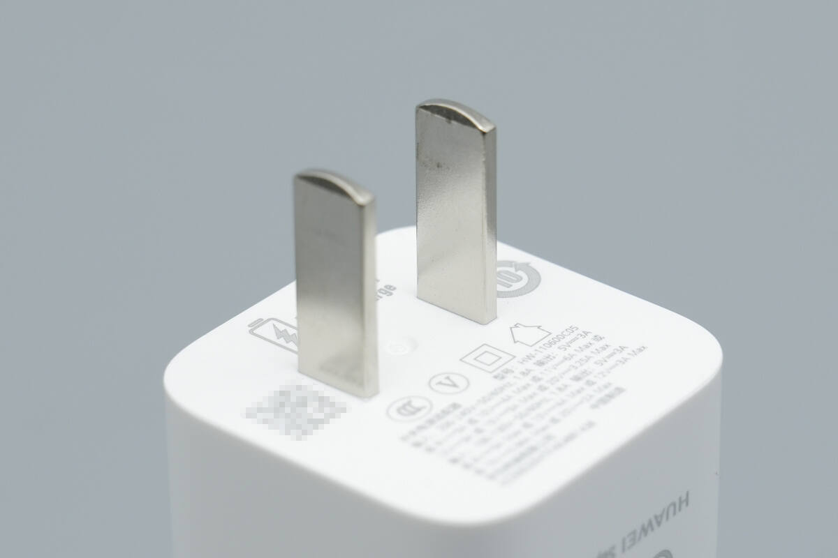
It is equipped with a fixed plug.
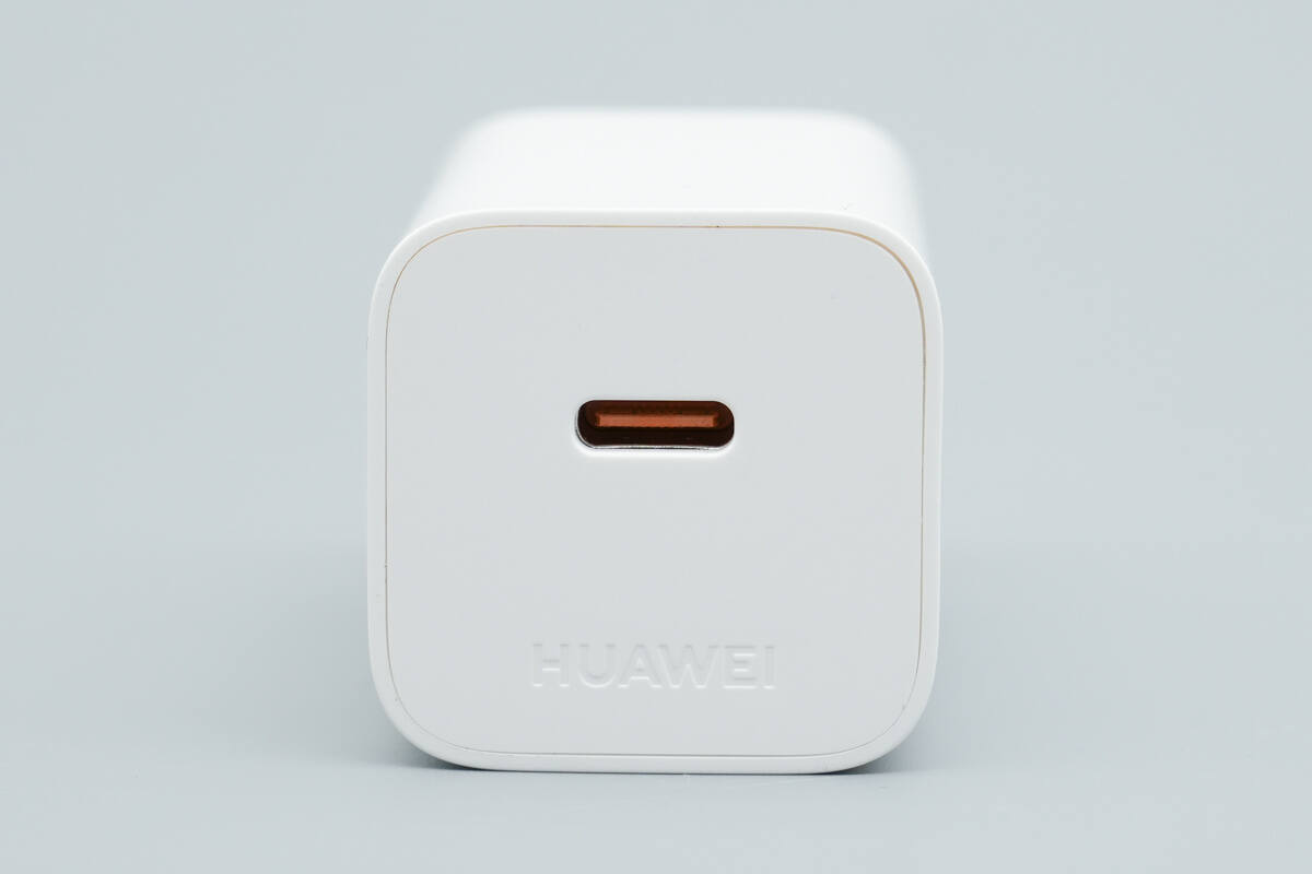
There is a USB-C output port on the top.
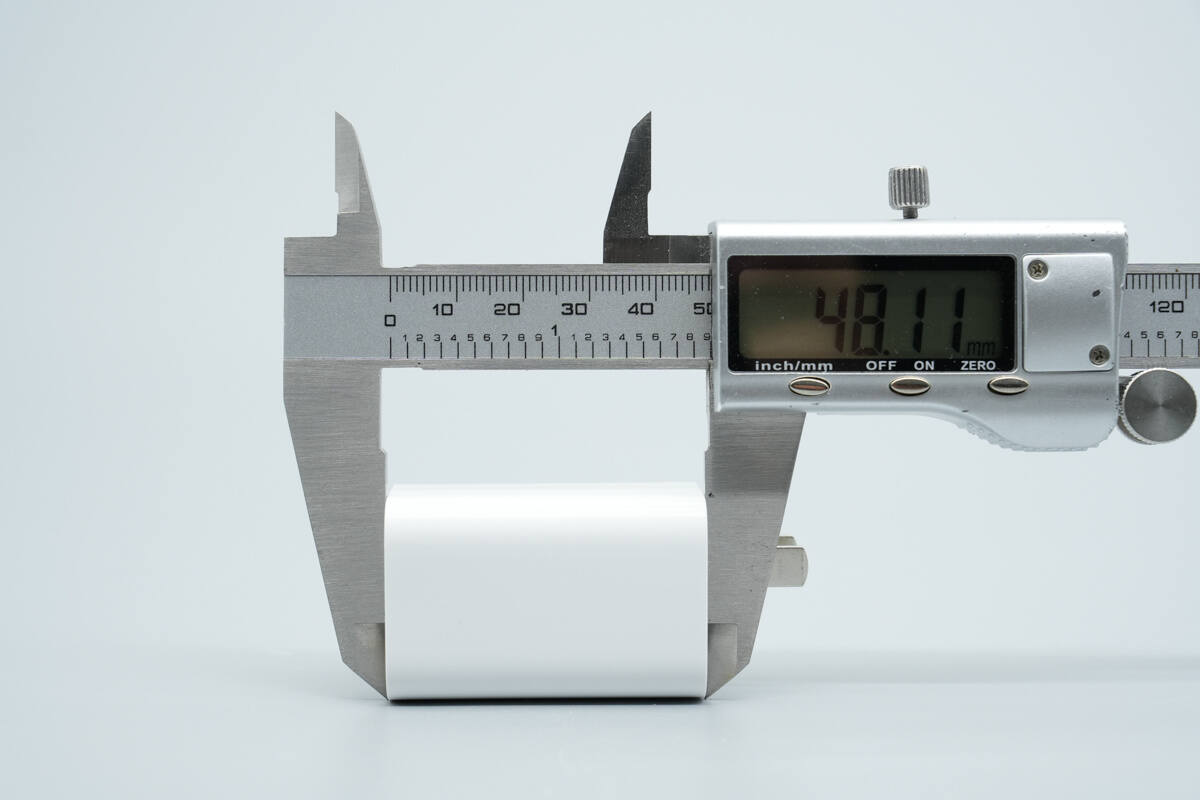
The length of the charger is about 48.11 mm (1.89 inches).

The width is about 31.01 mm (1.22 inches).
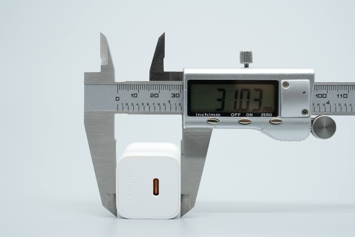
The thickness is about 31.03 mm (1.22 inches).
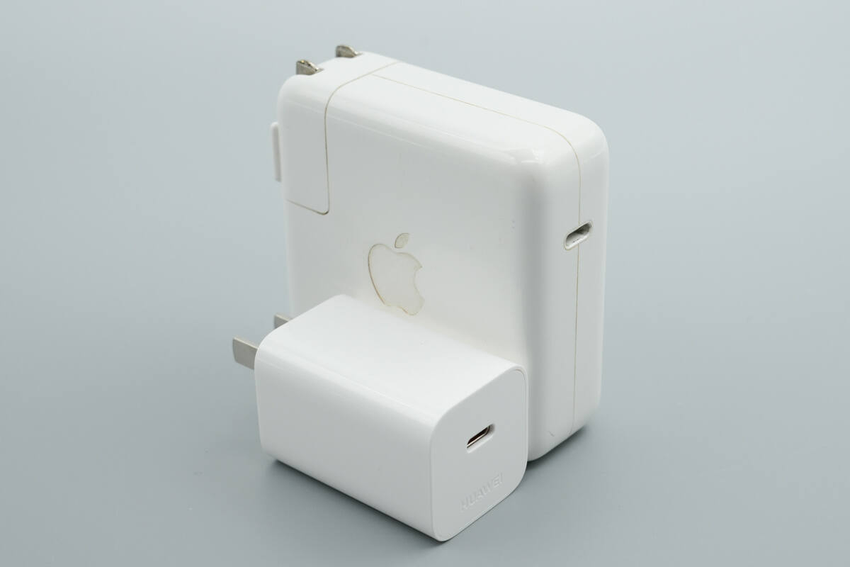
Compared with the Apple 67W charger, its size advantage is obvious.
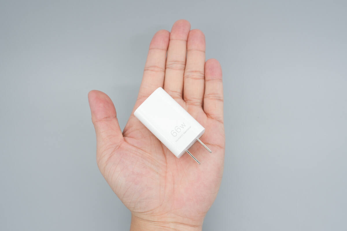
That's how big it is on the hand.
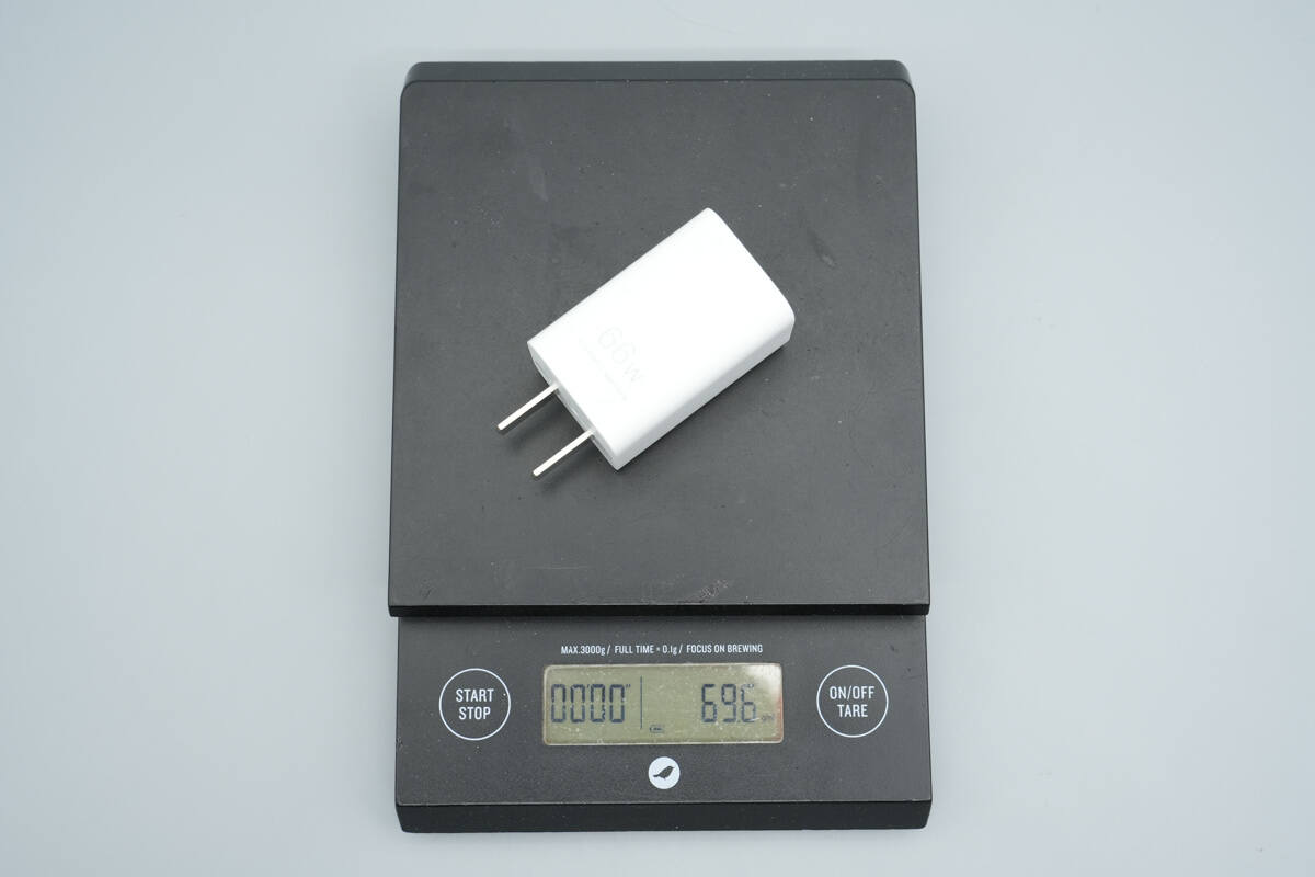
The weight is about 70 g (2.47 oz).
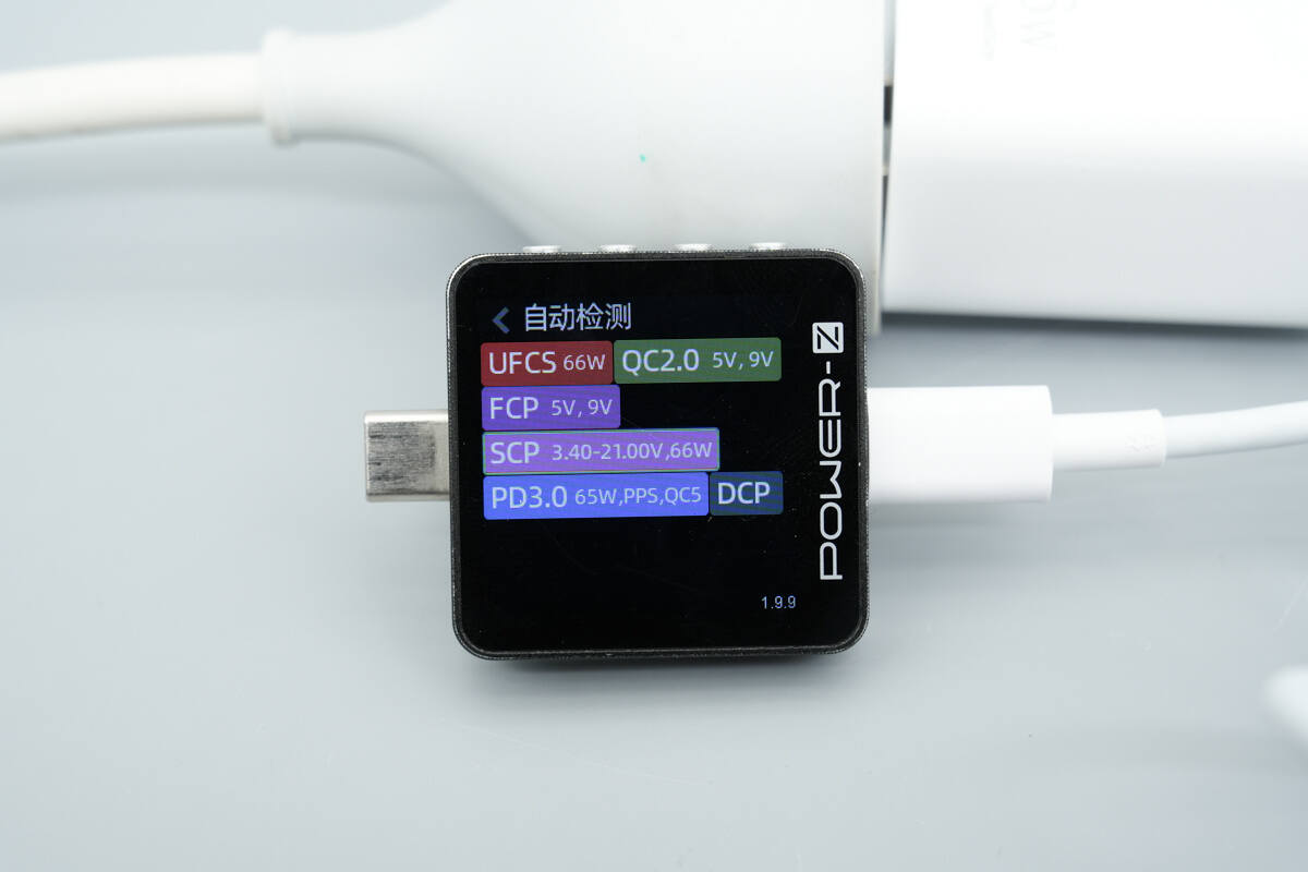
ChargerLAB POWER-Z KM003C shows that the USB-C1 supports FCP, SCP, QC2.0/5, PD3.0, PPS, and DCP protocol.
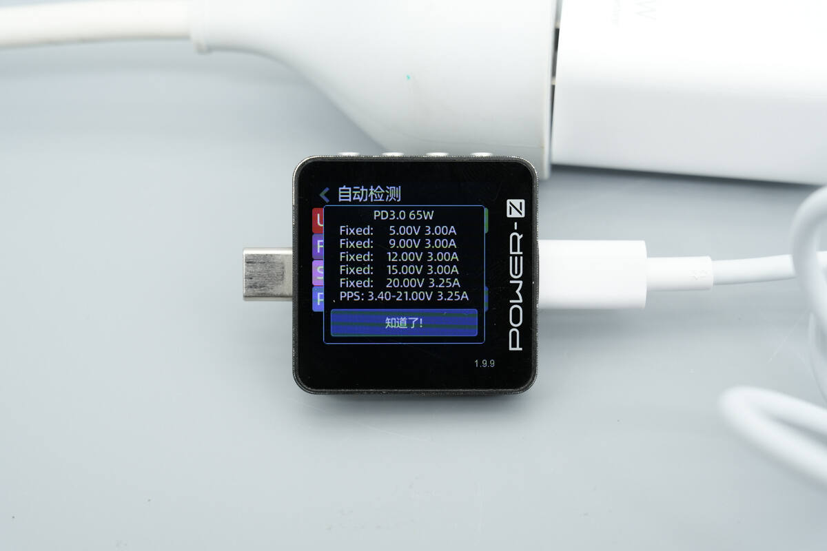
It has five fixed PDOs: 5V3A, 9V3A, 12V3A, 15V3A, and 20V3.25A, along with one set of PPS at 3.4-21V 3.25A.
Teardown
Next, let's take it apart to see its internal components and structure.
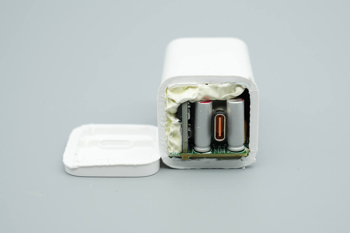
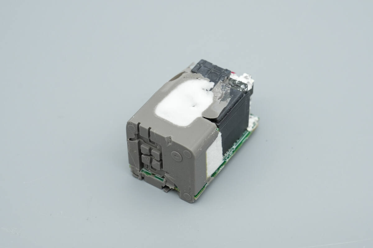
Cut open the top casing, and the internal PCB module is reinforced with white adhesive.
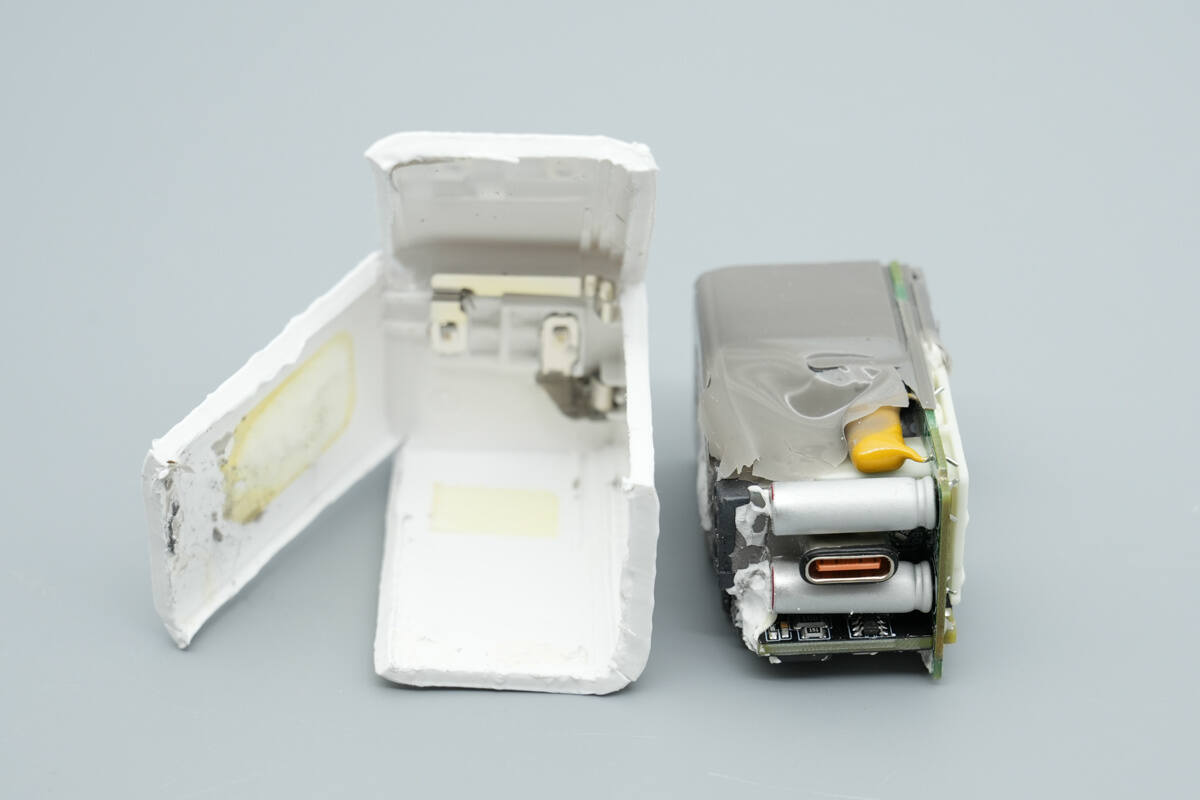
Remove the PCB module. The input side uses contact-type electrical connections.
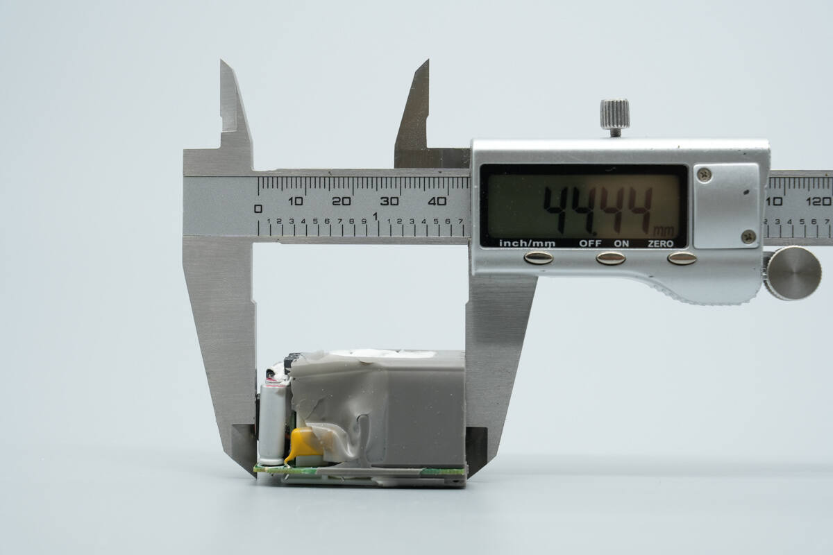
The length of the PCBA module is about 44.44 mm (1.75 inches).
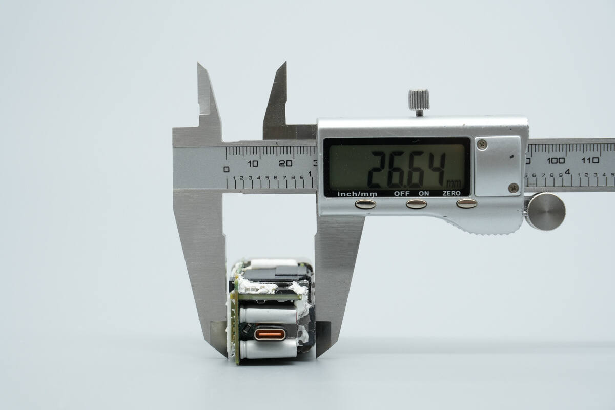
The width is about 26.64 mm (1.049 inches).
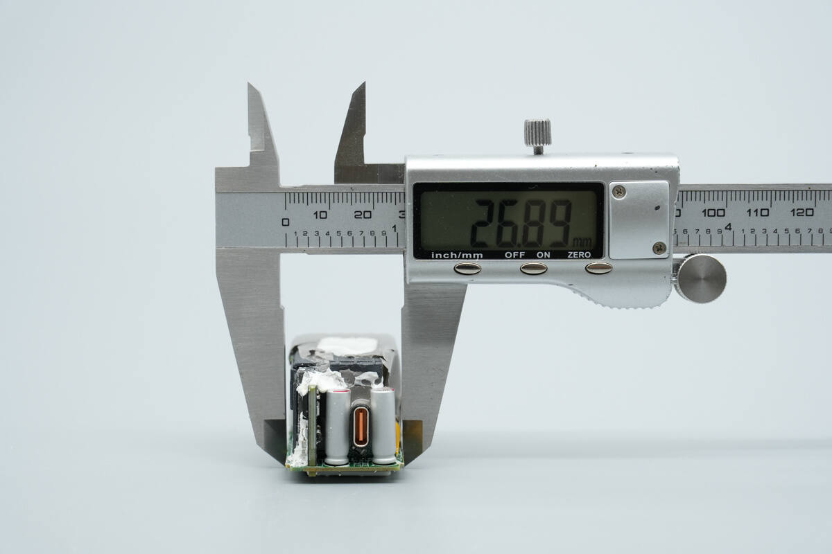
The thickness is about 26.89 mm (1.059 inches).
The input side is sealed and secured with thermally conductive adhesive.
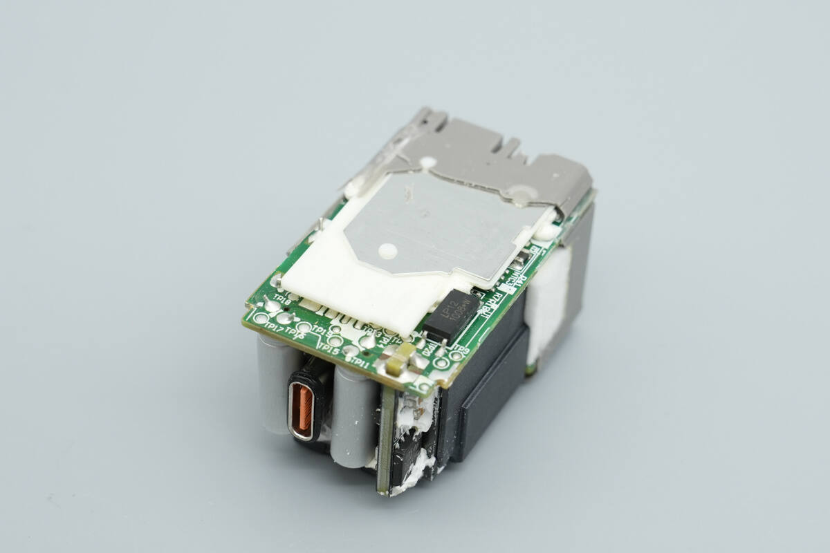
The back is covered with an insulating plastic plate and a heatsink.
After removing the thermally conductive adhesive and taking off the plastic plate, it is revealed that the plate also has an integrated barrier for isolating the primary and secondary sides.
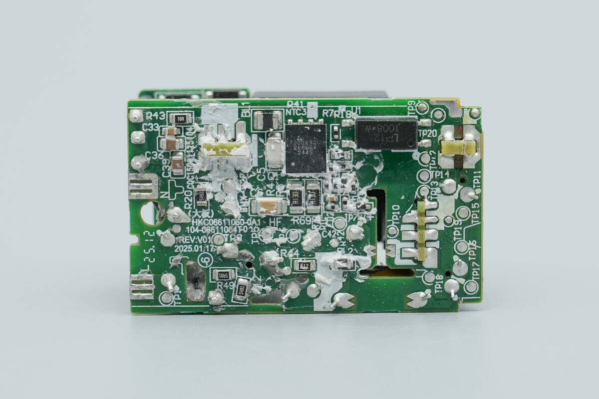
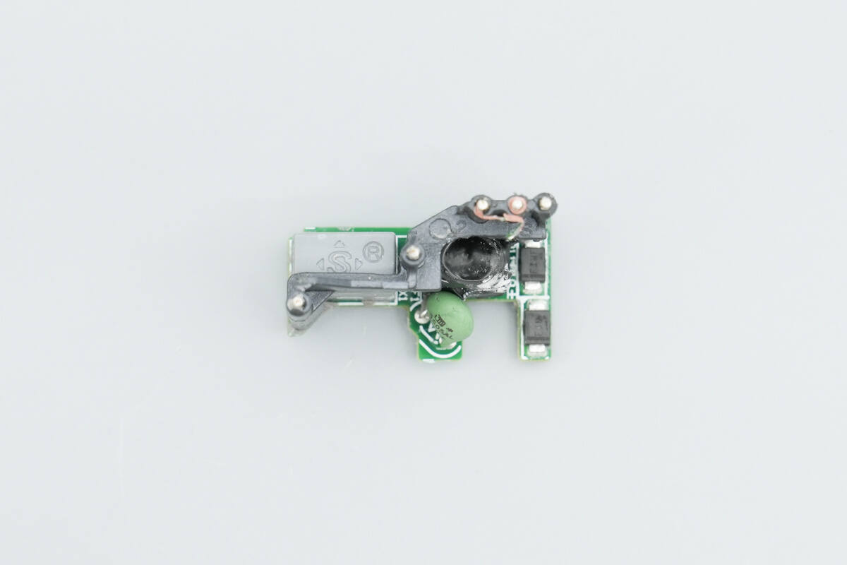
The back of the module is equipped with a primary MOSFET and an optocoupler.
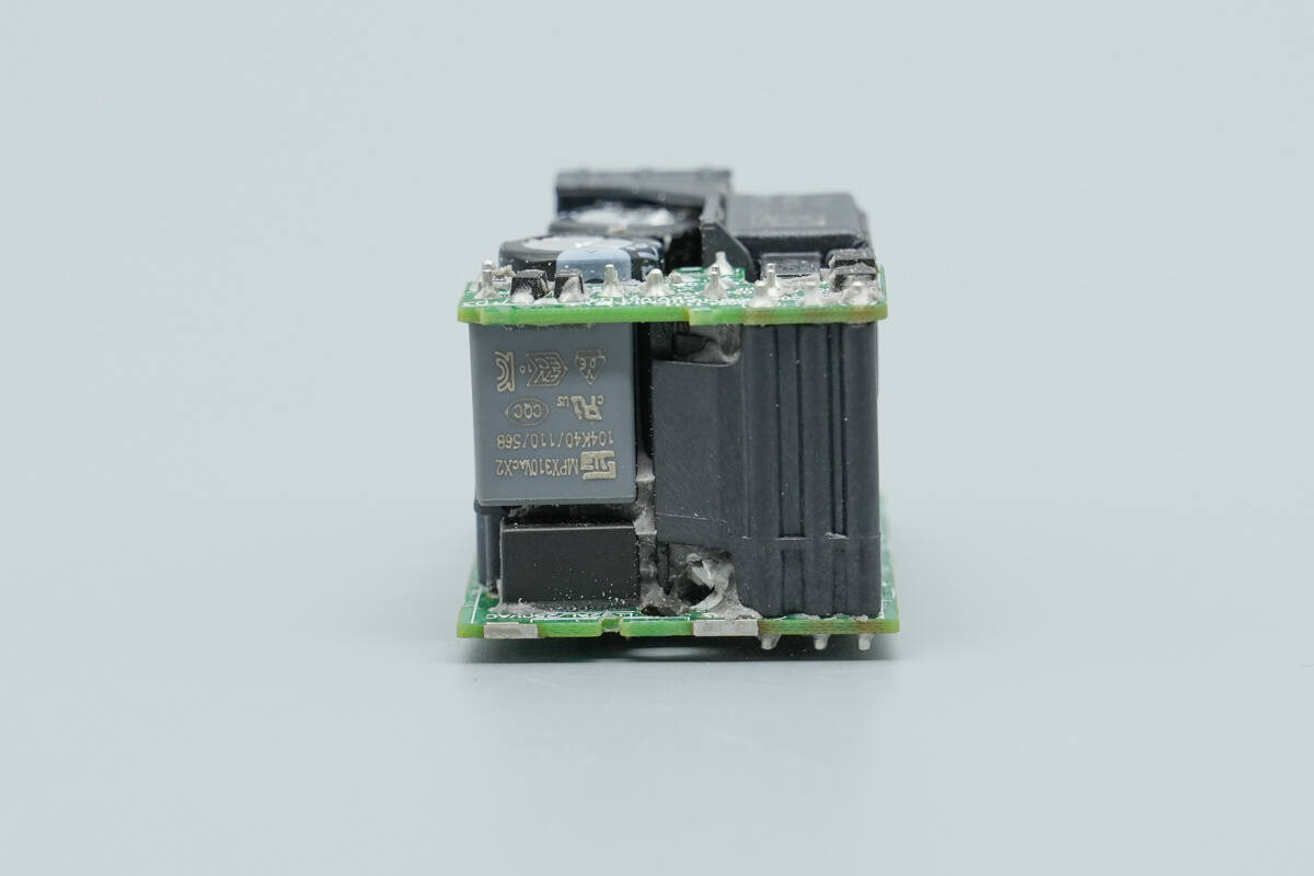
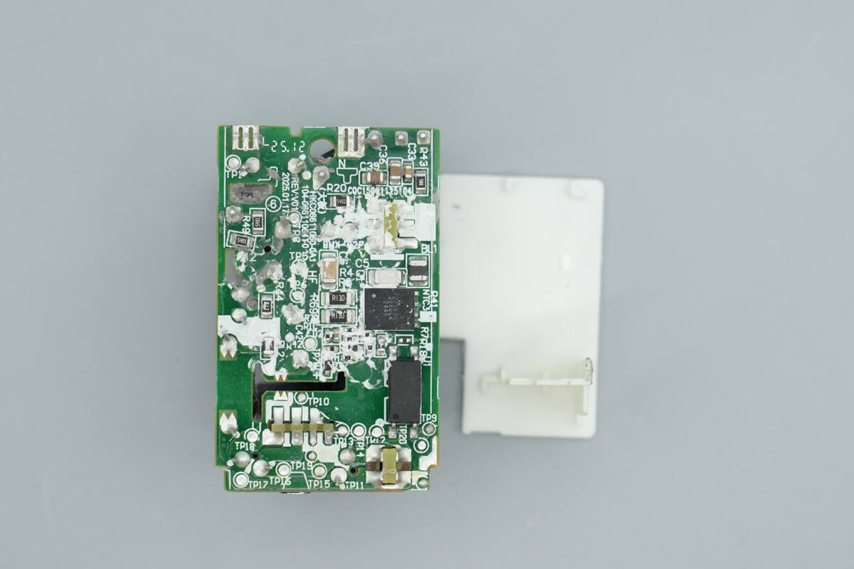
A small PCB is located at the top of the input side and is supported and secured to the main board via a plastic bracket.
A planar transformer PCB is mounted on this side.
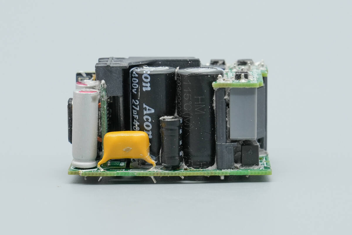
The opposite side is equipped with an I-shaped inductor, electrolytic capacitors, and other components.
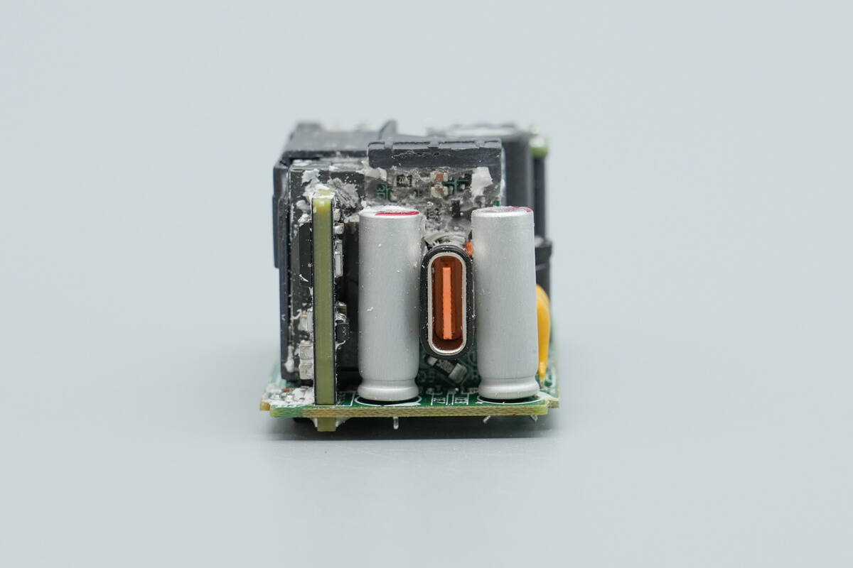
The output side features a small PCB with the USB-C socket and two solid capacitors.
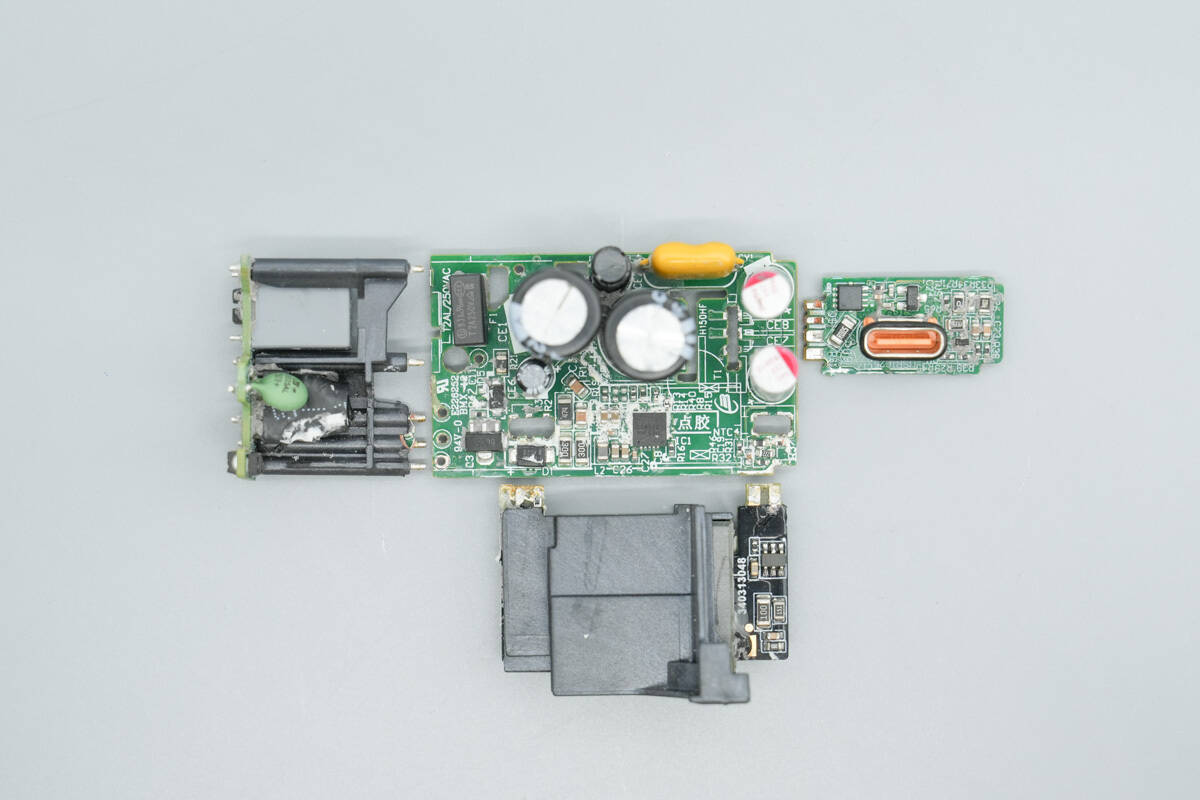
The PCB module is fully disassembled.
On the front of the small PCB at the top of the input side, there is an NTC thermistor, a safety X2 capacitor, and a common mode choke. Besides the common mode choke, there are also two rectifier diodes.
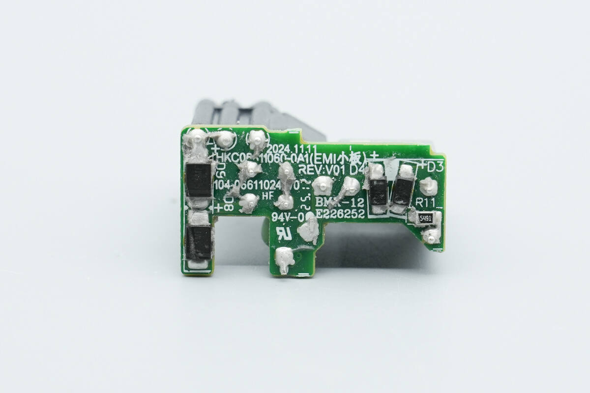
The other two rectifier diodes are located on the back of the PCB, forming a bridge rectifier together with the front two diodes.
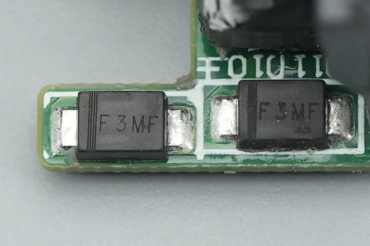
Close-up of the two rectifier diodes.
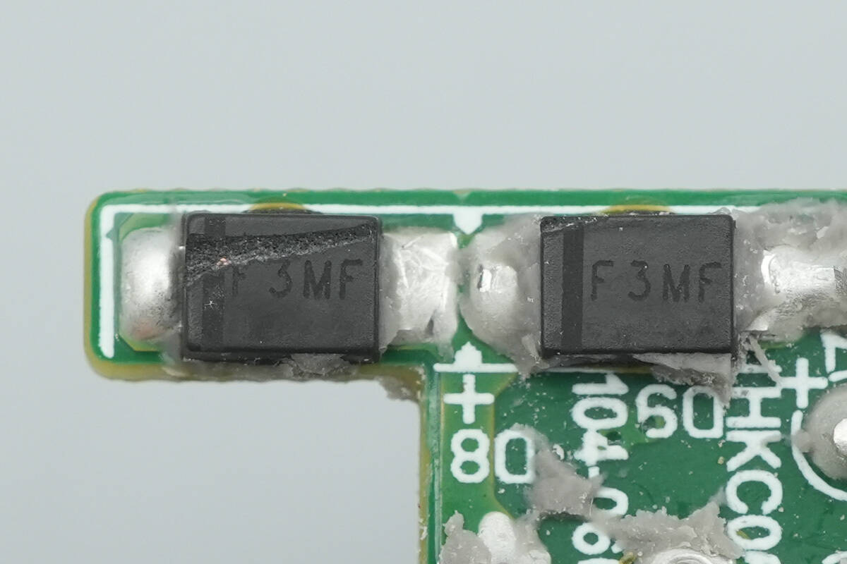
Close-up of the other two.
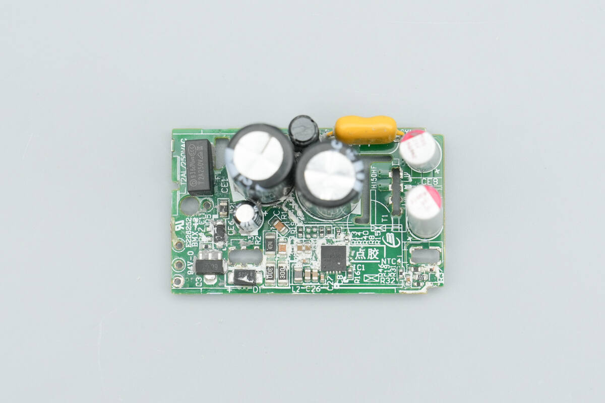
The front of the main board is equipped with a time-delay fuse, a master control chip, capacitors, and other components.
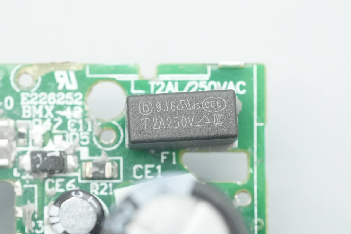
The time-delay fuse is from Betterfuse, part number 936, rated at 2A 250V.
The NTC thermistor is used to suppress inrush current at power-up.
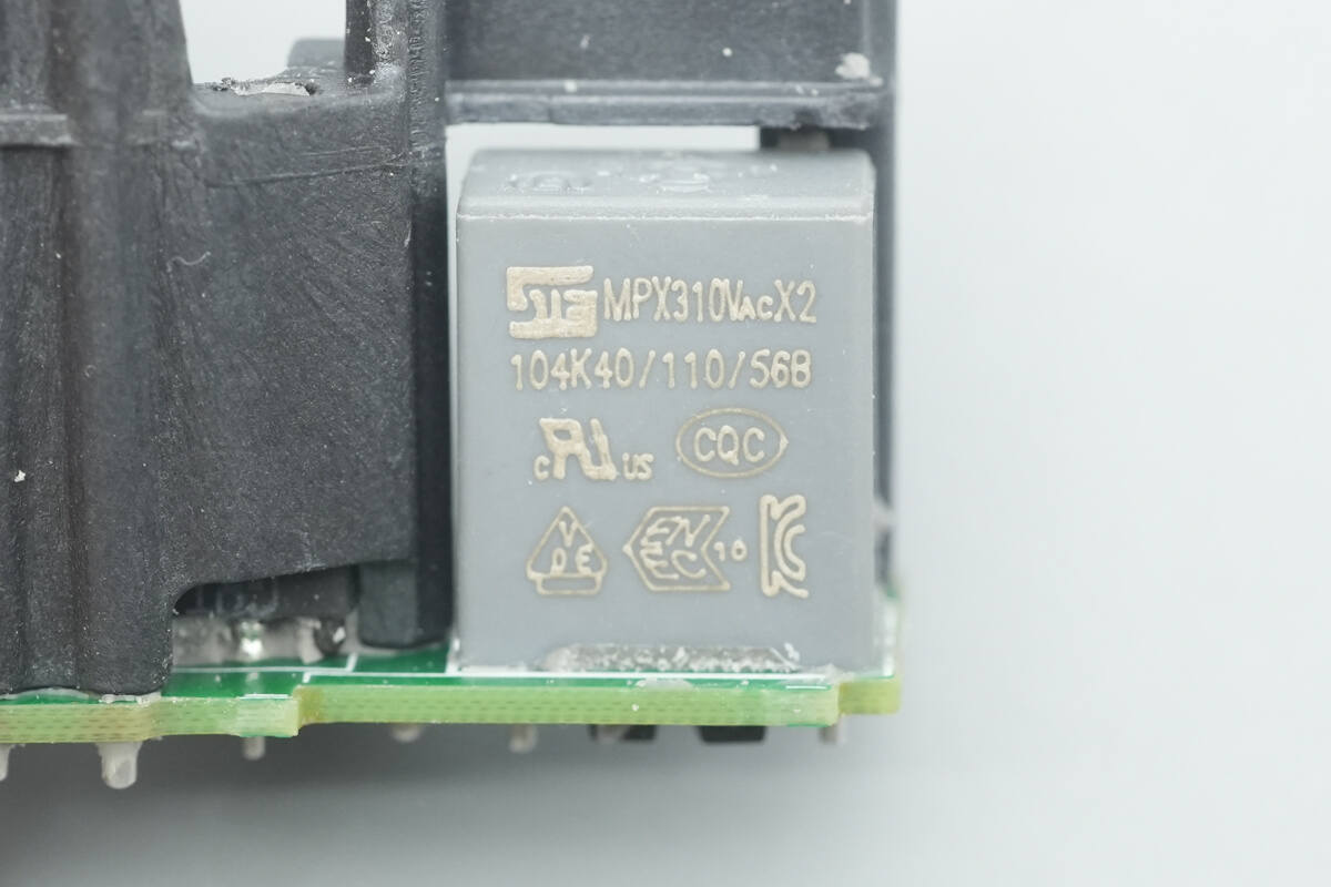
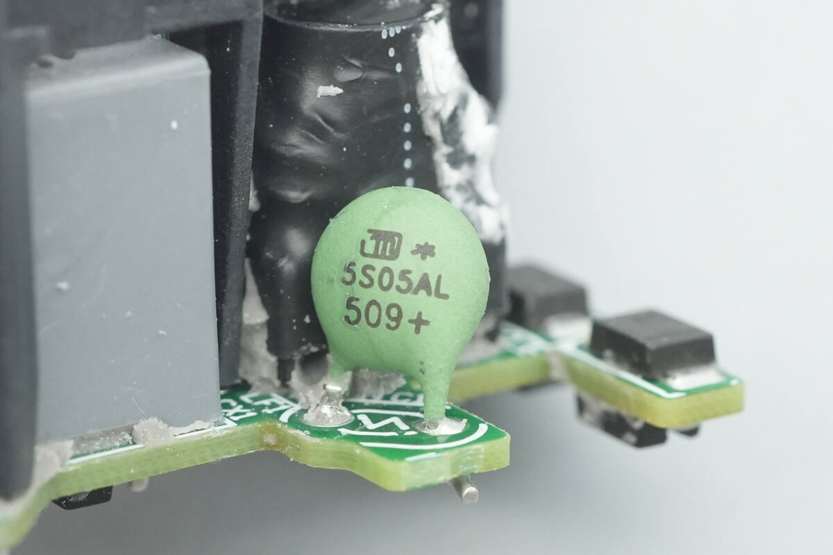
The safety X2 capacitor is from STE, with a capacitance of 0.1 μF.
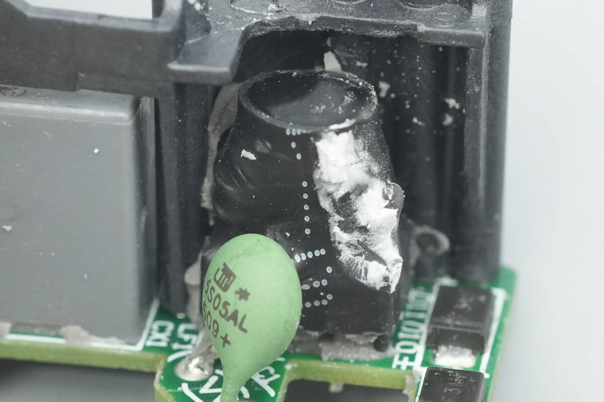
The common mode choke is used to filter EMI interference and is insulated with a heat-shrink sleeve for protection.
The I-shaped inductor is insulated and protected with heat-shrink tubing.
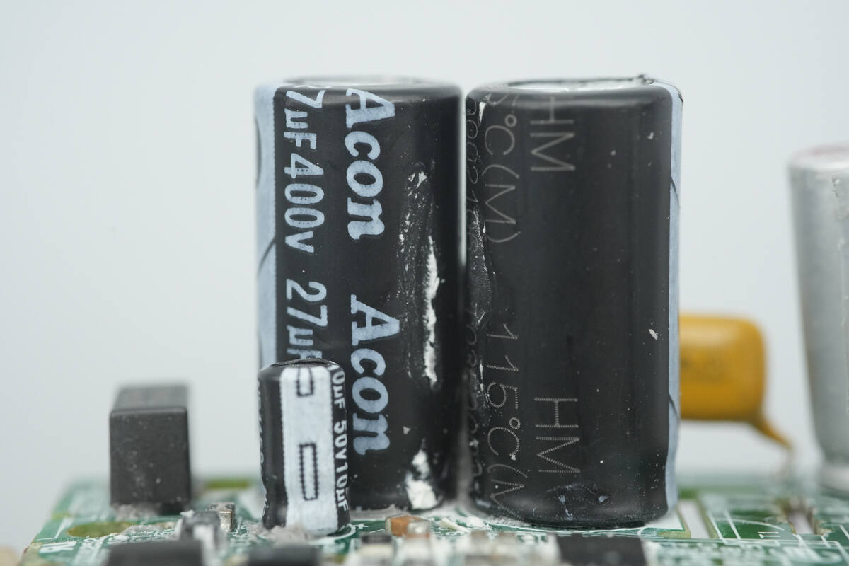
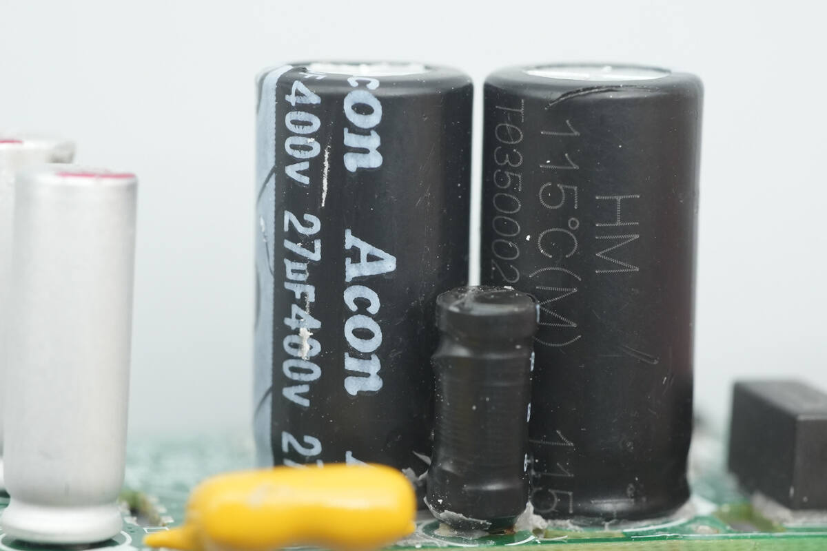
Two high-voltage filter electrolytic capacitors are sourced from Acon, each with a rating of 400 V and 27 μF.
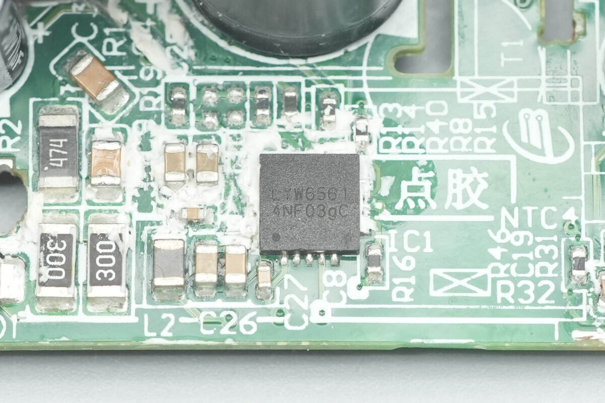
The master control chip is marked with LYW6561.
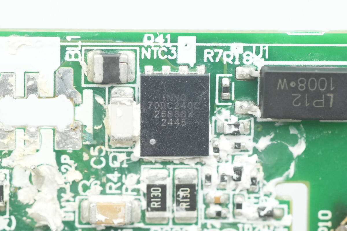
The primary MOSFET is sourced from Innoscience, model INN700DC240C. It is a 700 V enhancement-mode GaN FET with an on-resistance of 240 mΩ, compliant with JEDEC industrial application standards. It features integrated ESD protection and is packaged in a DFN 5 × 6 form factor.
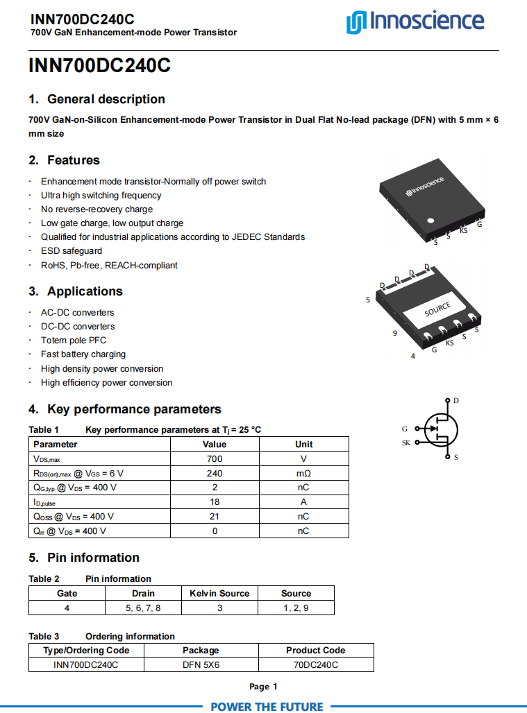
Here is the information about Innoscience INN700DC240C.
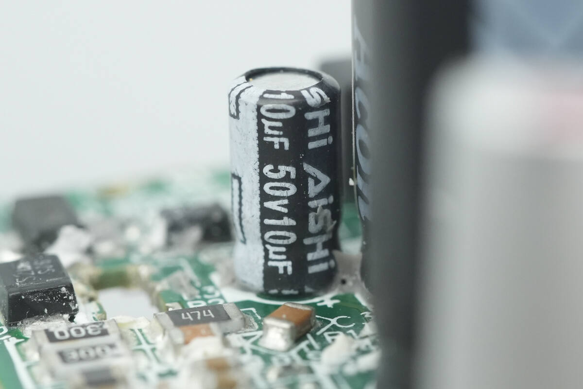
The capacitor supplying power to the master control chip is sourced from AiSHi, with a rating of 50 V and 10 μF.
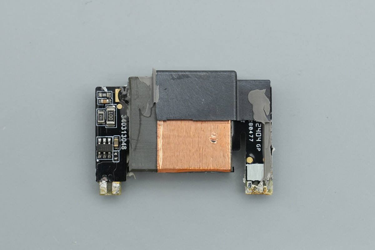
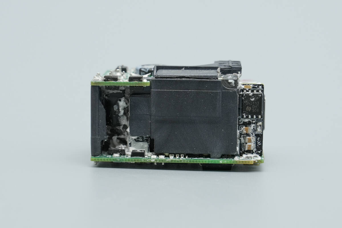
The planar transformer module has its magnetic core wrapped with copper foil, and a synchronous rectifier controller is located on the left side.
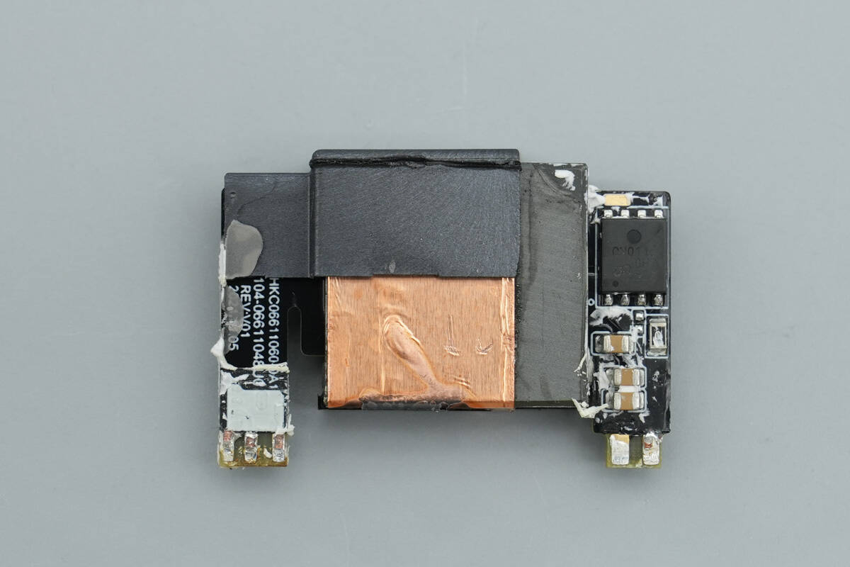
A synchronous rectifier is installed at the corresponding position on the back side.

After breaking the magnetic core, the racetrack-shaped windings inside the planar transformer are revealed.
A 1018 optocoupler is used for output voltage feedback.
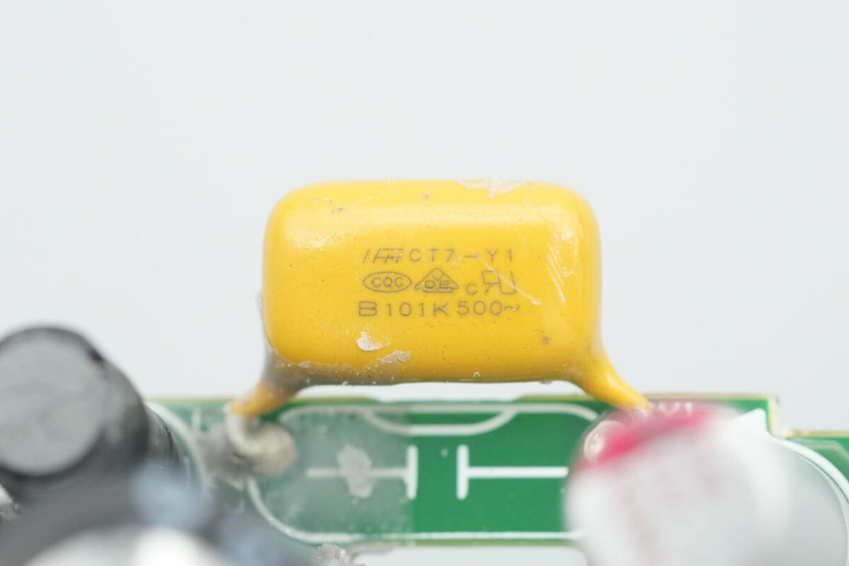
The safety Y capacitor is a CT7 series series-connected Y capacitor, using a yellow resin encapsulation.
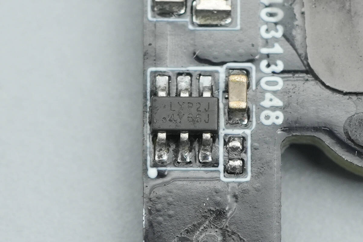
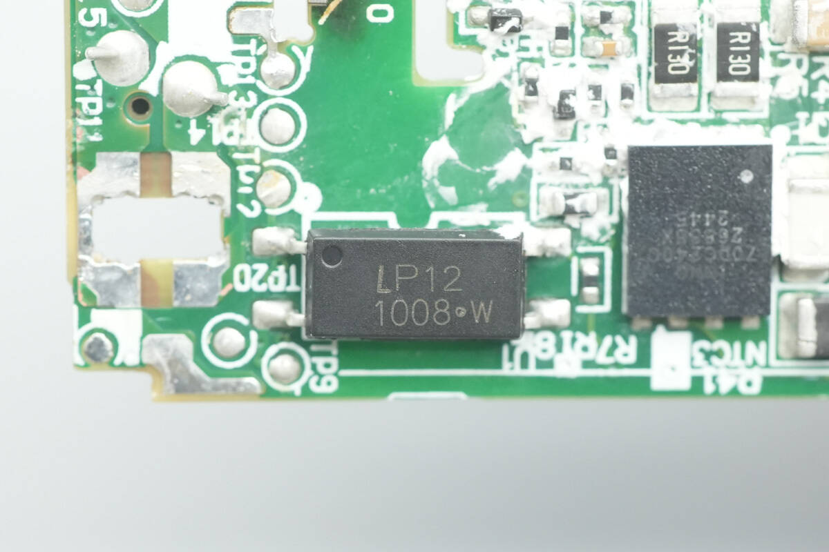
The synchronous rectifier controller is marked with LYP2J.
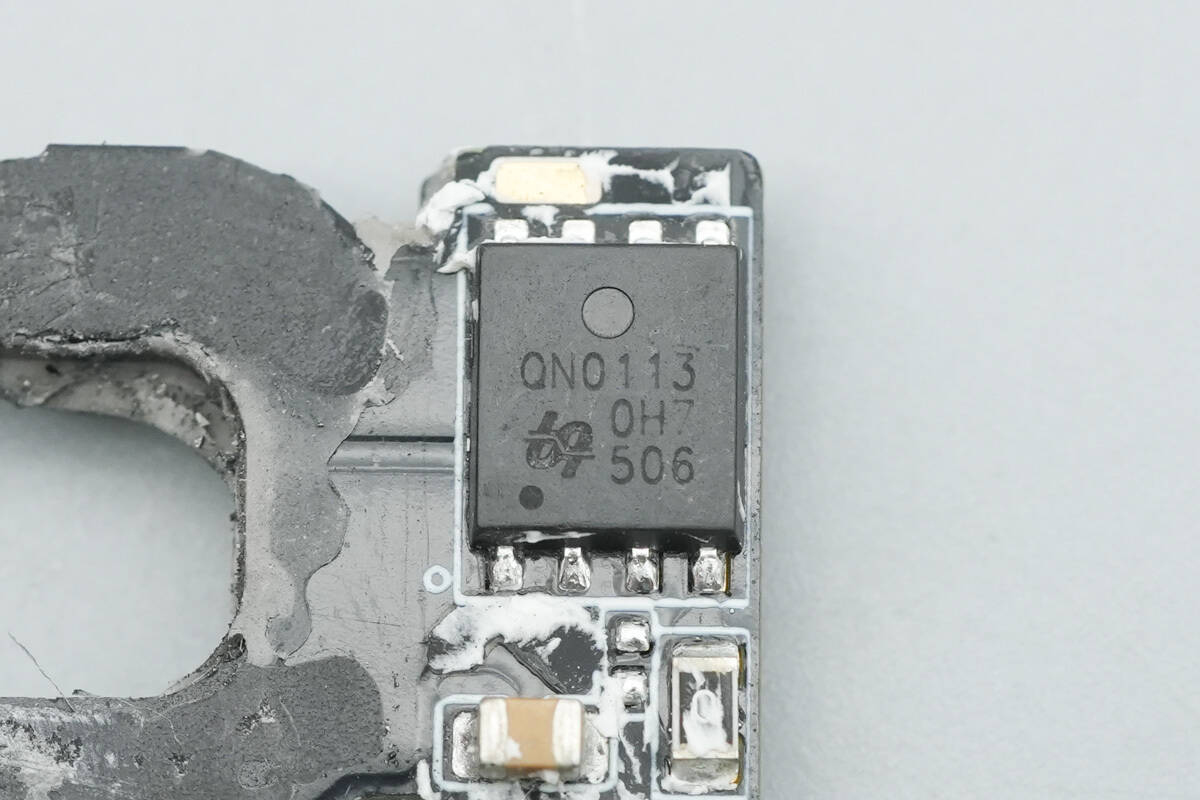
The synchronous rectifier is from uPI, model QN0113M6N. It is an NMOS with a voltage rating of 100 V and an on-resistance of 6 mΩ, packaged in a PRPAK 5 × 6 form factor.
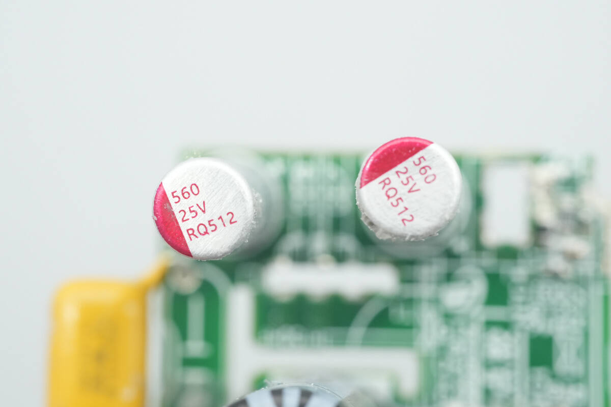
Two output solid capacitors are rated at 25 V and 560 μF each.
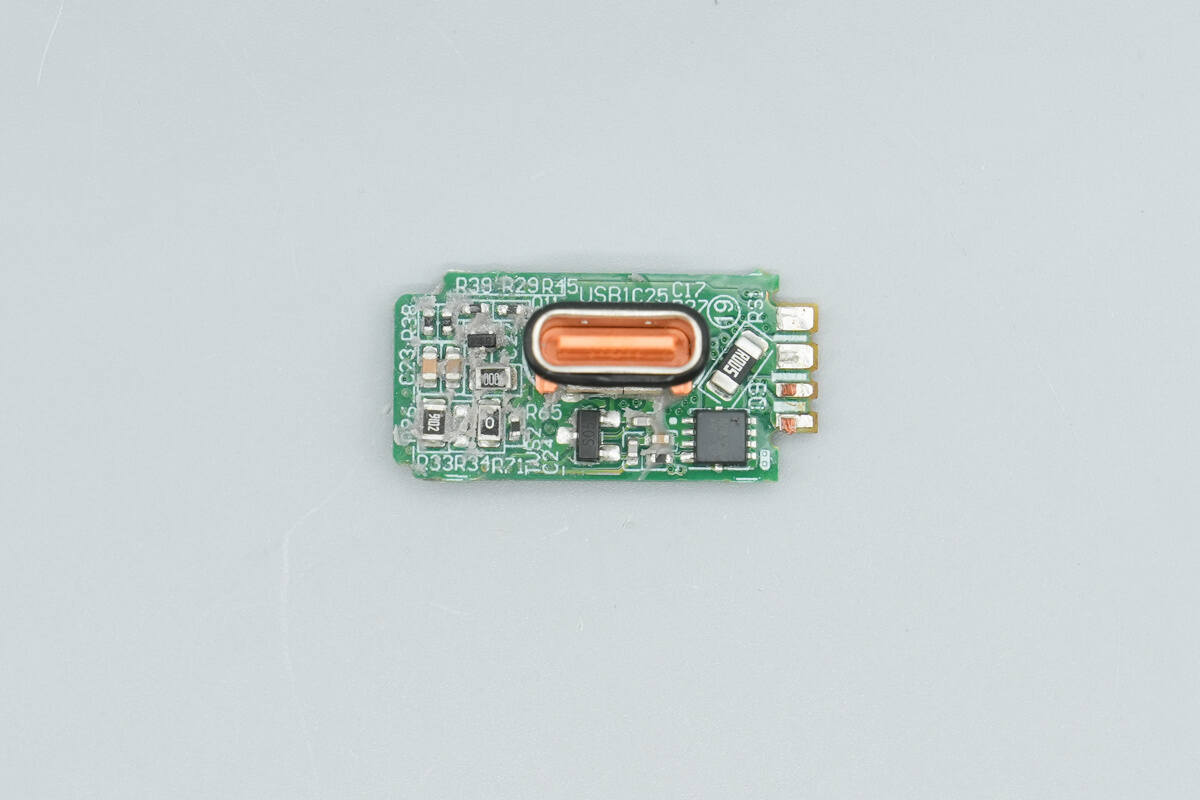
There is an output VBUS MOSFET on the front side of the output PCB.
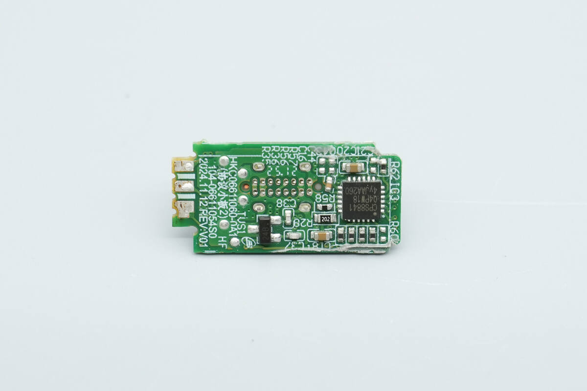
A protocol chip is installed on the back side.
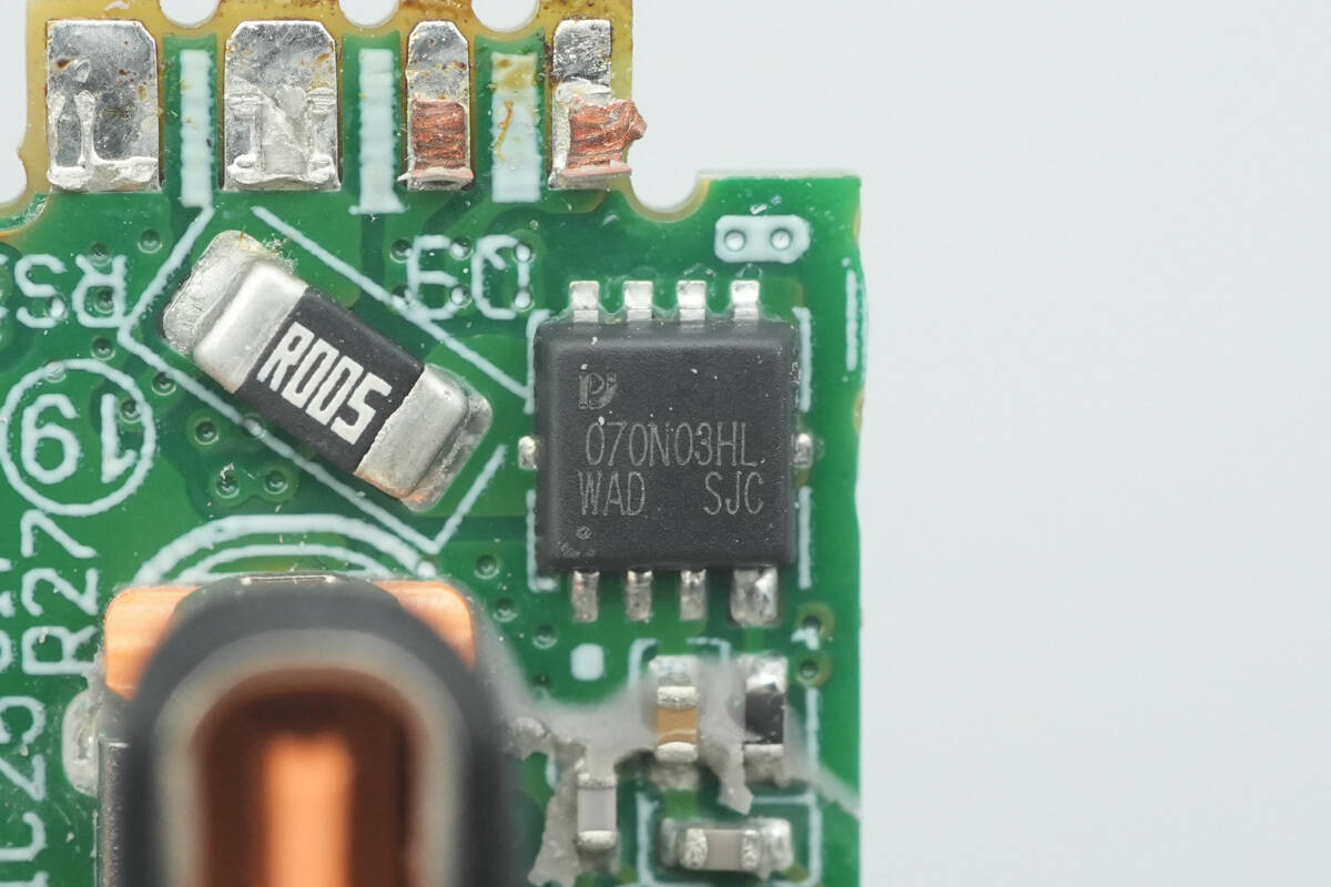
The output VBUS MOSFET is sourced from PY, marked 070N03HL, and is packaged in a DFN 3 × 3 form factor.
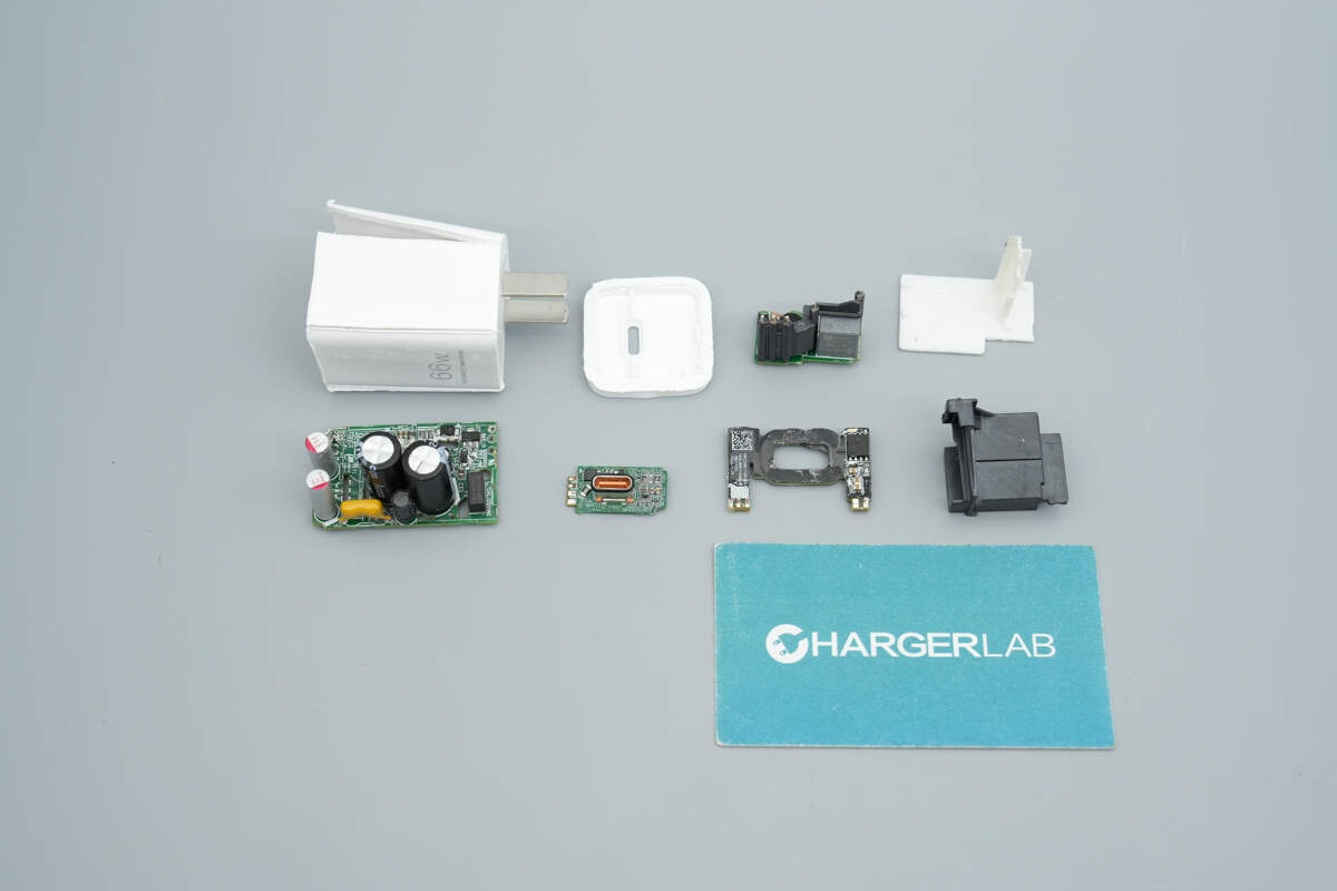
Well, those are all components of the Huawei SuperCharge 66W GaN Charger for Mate 80.
Summary of ChargerLAB
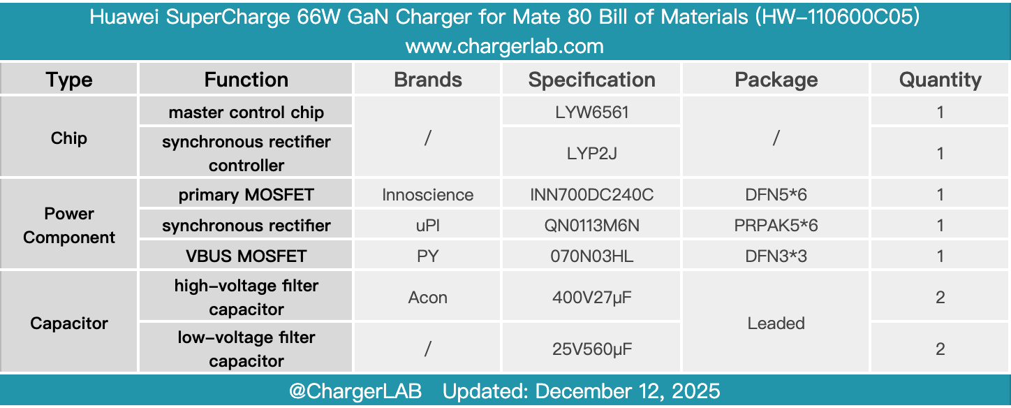
Here is the component list of the Huawei SuperCharge 66W GaN Charger for Mate 80 for your convenience.
It features a stacked architecture, and with GaN technology, it achieves a significant breakthrough in power density. It not only supports Huawei 66 W SuperCharge but also 65 W PD/PPS, making it highly compatible with Huawei devices while also capable of fast charging third-party smartphones, tablets, and laptops.
After taking it apart, we found that the PCBA module uses multiple small PCBs stacked together. It employs a high-efficiency power design, supports intelligent temperature control, and features 12 protection functions, including short-circuit, overcurrent, overvoltage, and undervoltage. The input side is potting-treated and uses Innoscience GaN devices. The product maintains Huawei’s consistent high standard of materials and craftsmanship.
Related Articles:
1. Teardown of Huntkey 140W GaN Charger (HKC14028050-0B1)
2. Teardown of NIU 280W E-bike Charger (DZL482015N)
3. Teardown of GreatWall SPARK 850W GaN 80 PLUS Gold Fully Modular Power Supply (G-850)