Introduction
On March 20th, at the Huawei Pura Product Launch, the first smartphone fully equipped with HarmonyOS 5—Huawei Pura X—was officially unveiled, marking the full transition of Huawei’s terminals into the HarmonyOS era. The new device is equipped with a 4720mAh high-silicon anode battery and supports 66W wired and 40W wireless charging, eliminating users' charging anxiety.
Next, we'll teardown the Huawei 66W GaN charger, which is the included charger of the Huawei Pura X. Its compact design maximizes portability. It supports Huawei 66W SuperCharge, 66W UFCS, and 65W PD fast charging, making it an ideal companion for devices like the Mate 70 series/Pura X, as well as fast charging for smartphones and laptops from brands like Apple and Samsung.
Product Appearance
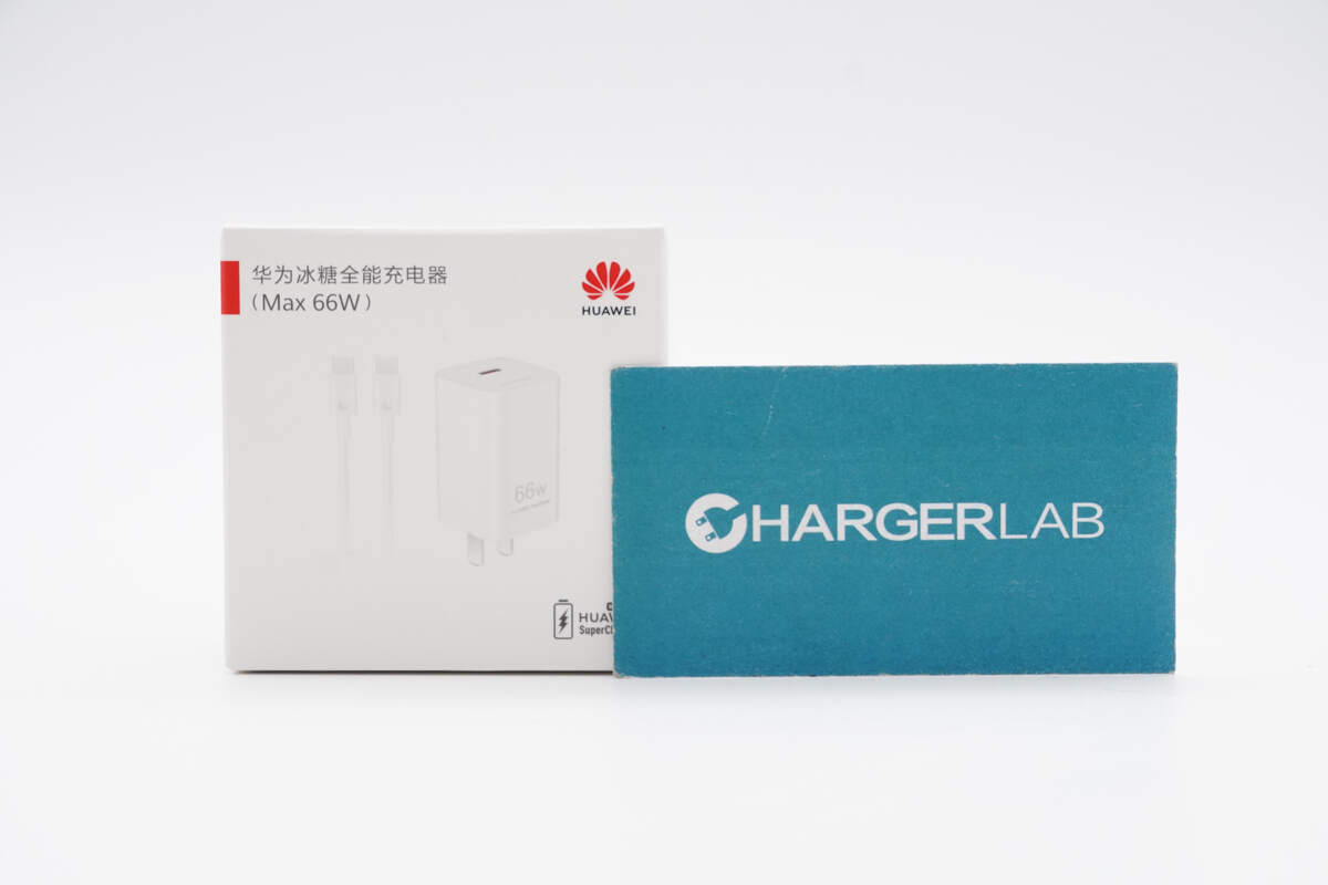
The packaging is printed with the Huawei logo, name, product appearance, and HUAWEI SuperCharge logo.
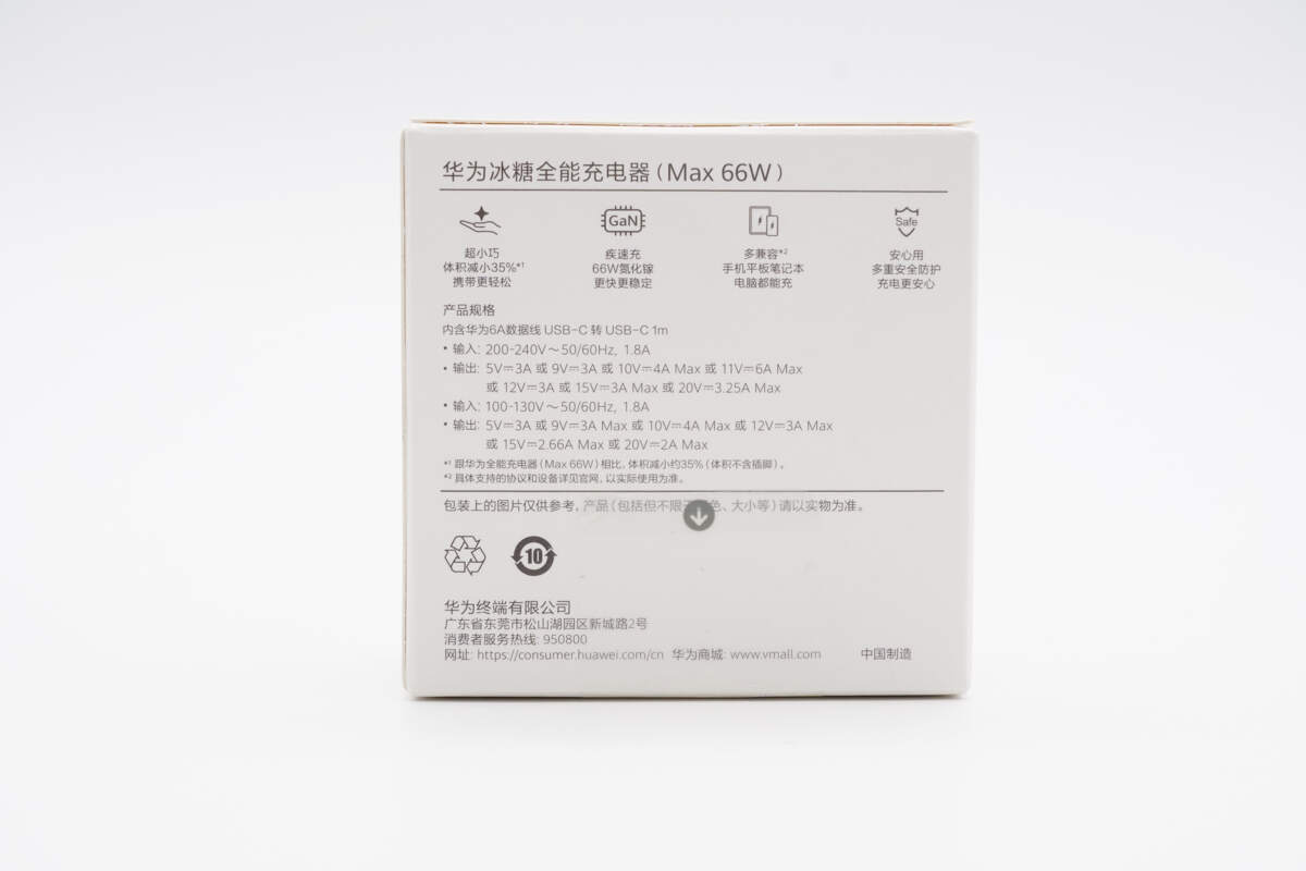
The specs info and selling points are printed on the back.
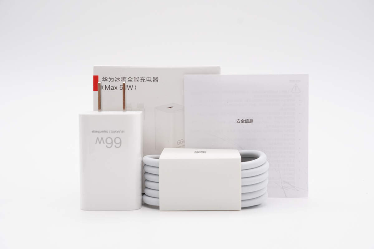
The packaging contains the charger, cable, and some documents.
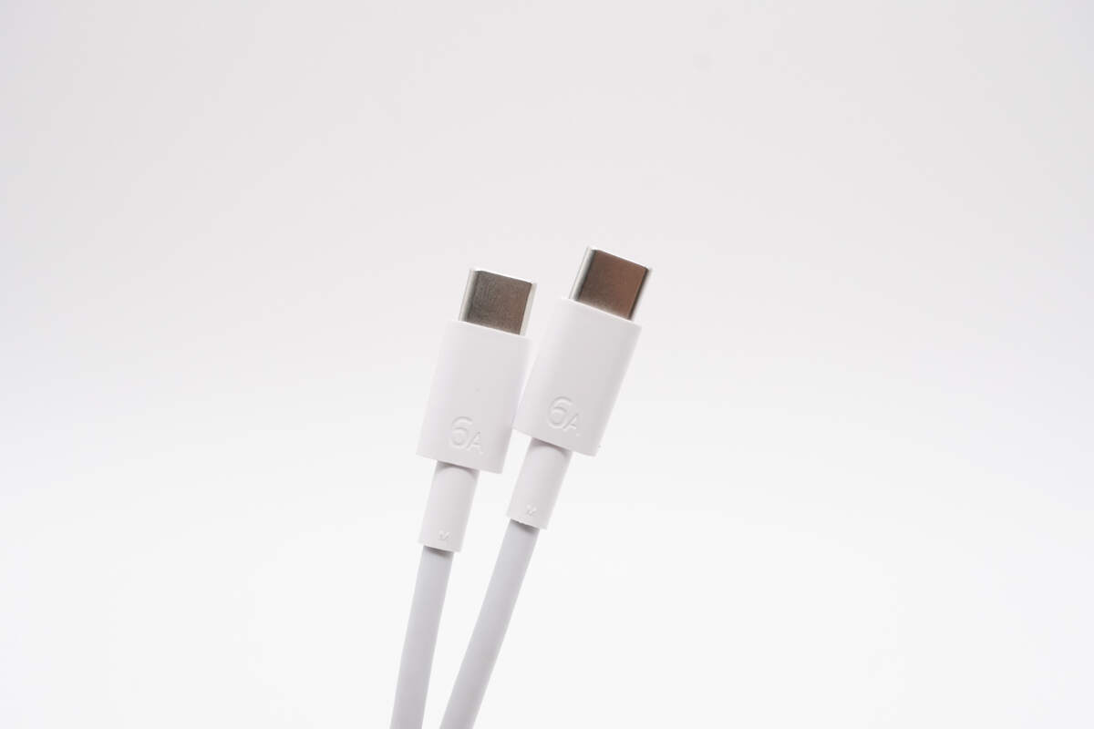
The dual USB-C cable is engraved with 6A.
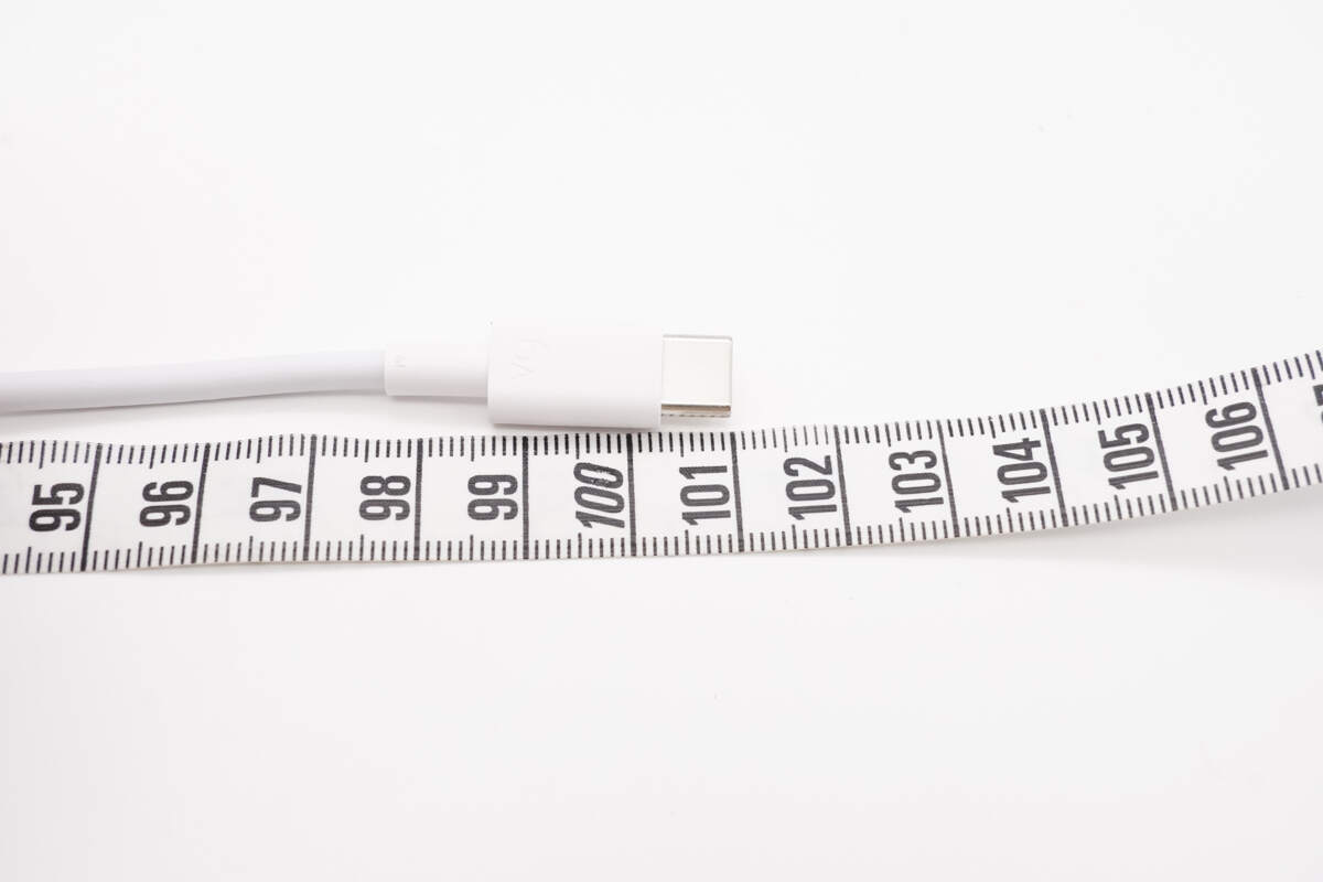
The length of the cable is about 1 m (3' 3.37'').
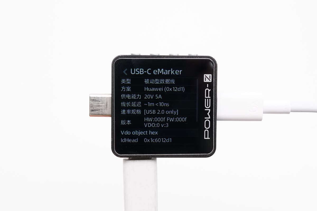
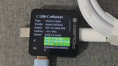
ChargerLAB POWER-Z KM003C shows it has an E-marker chip, supports 20V5A, and USB 2.0.
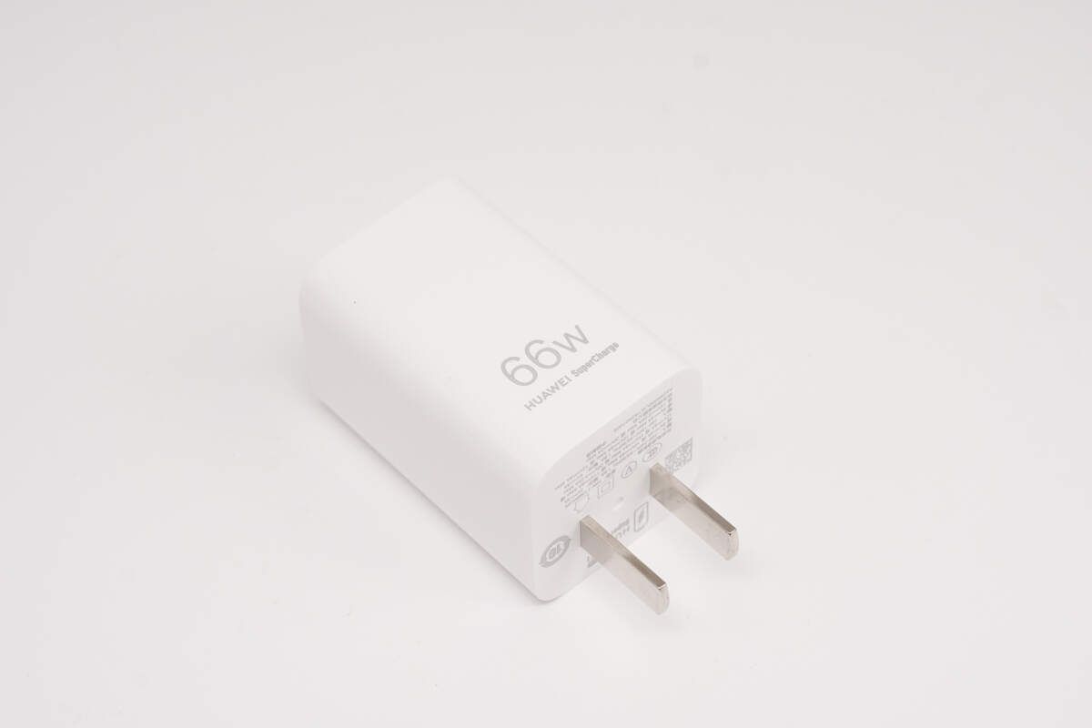
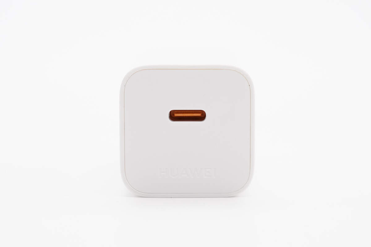
The charger is simple in design, small, and exquisite.
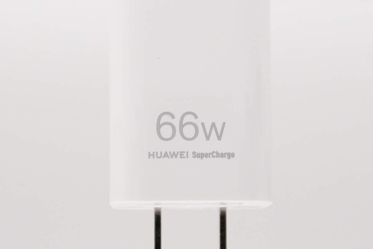
66W and HUAWEI SuperCharge are printed on the front.
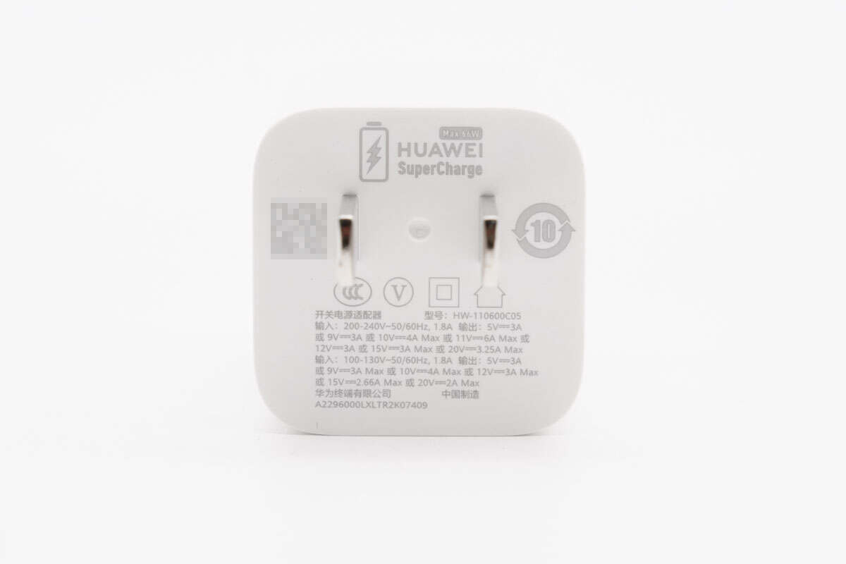
Model: HW-110600C05
Input: 200-240V~50/60Hz 1.8A
Output: 5V3A, 9V3A, 10V4A, 11V6A, 12V3A, 15V3A, 20V3.25A Max
Input: 100-130V~50/60Hz 1.8A
Output: 5V3A, 9V3A, 10V4A, 12V3A, 15V2.66A, 20V2A Max
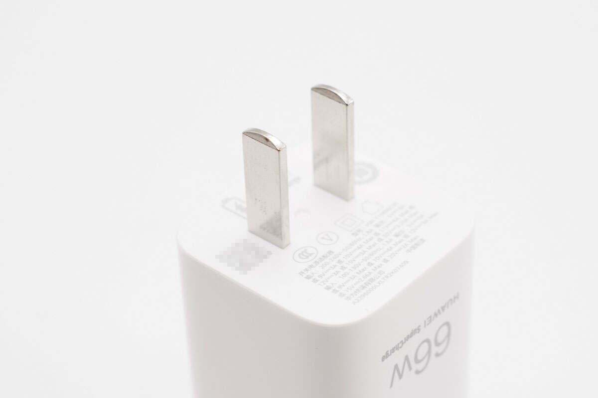
It adopts a fixed plug.
The plastic sheet is orange.
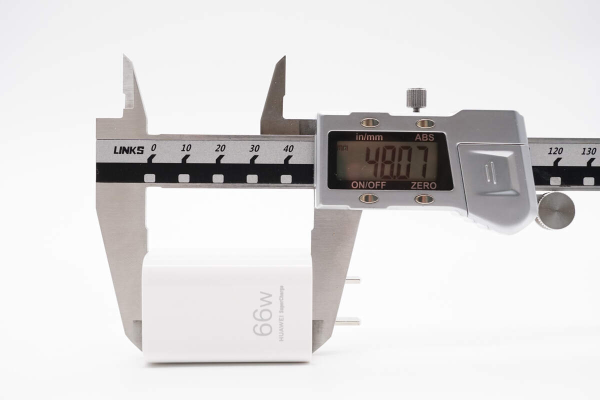
The length of the charger is about 48.07 mm (1.89 inches).
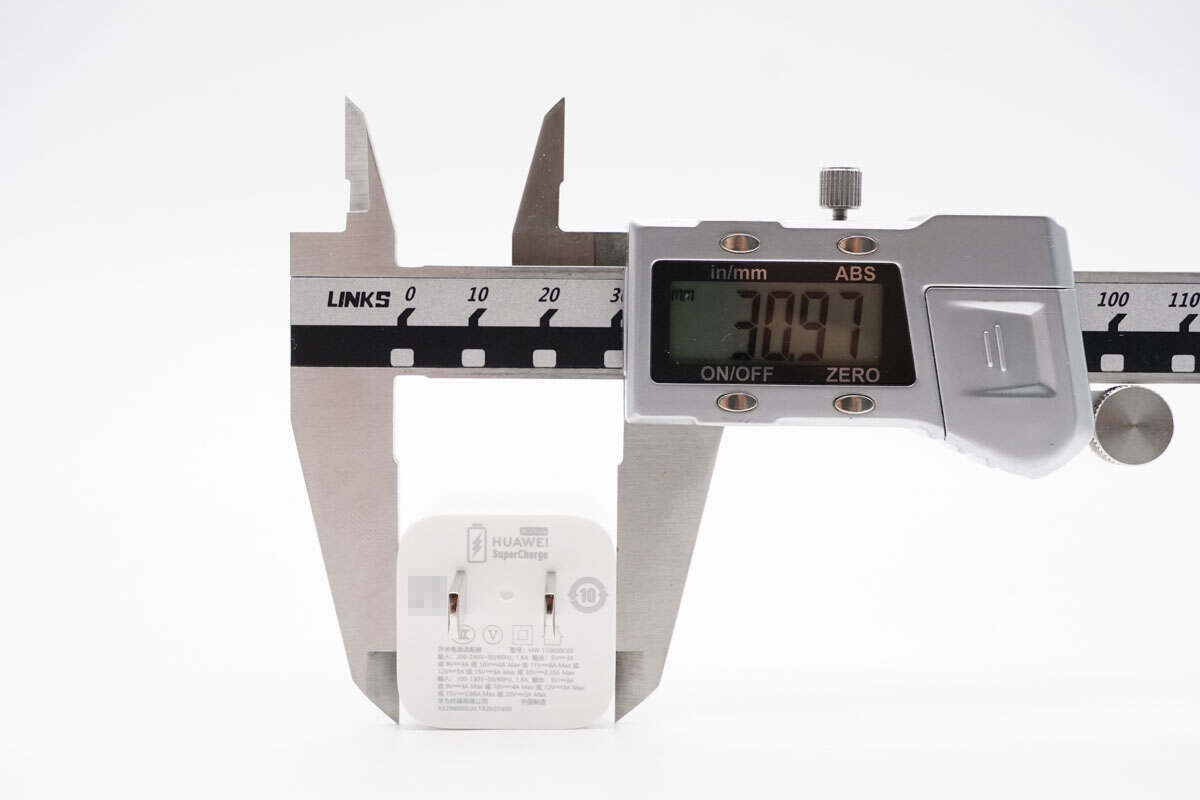
The width is about 30.97 mm (1.22 inches).
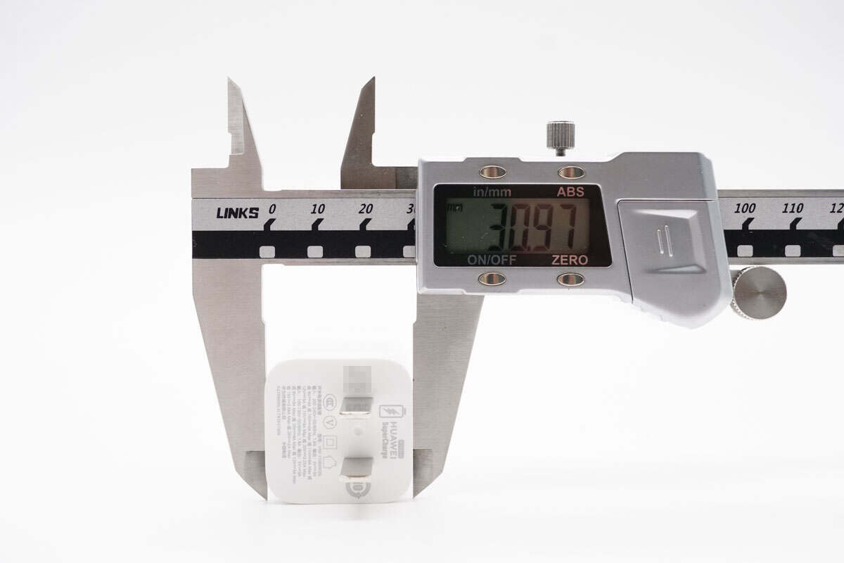
The thickness is about 30.97 mm (1.22 inches). The volume is about 46.11cm³, and the power density is about 1.43W/cm³.
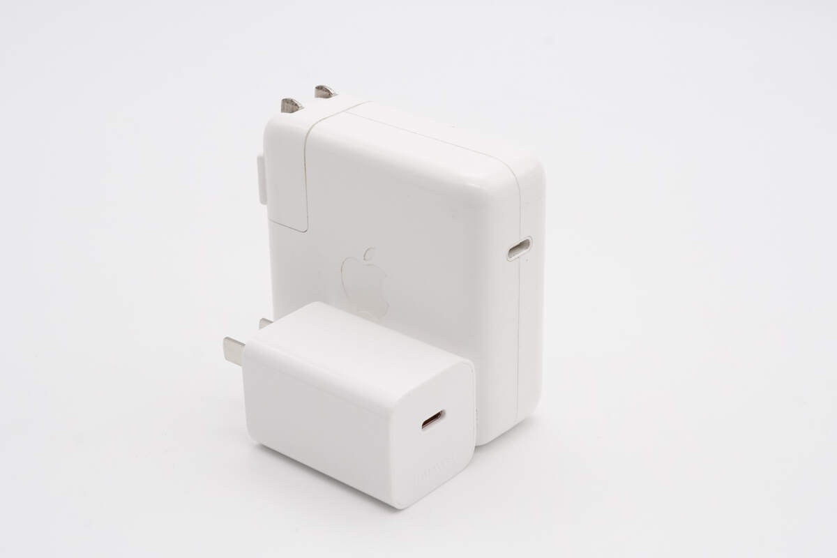
It is much smaller than the Apple 61W charger.
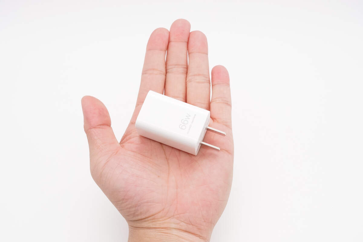
That's how big it is in the hand.
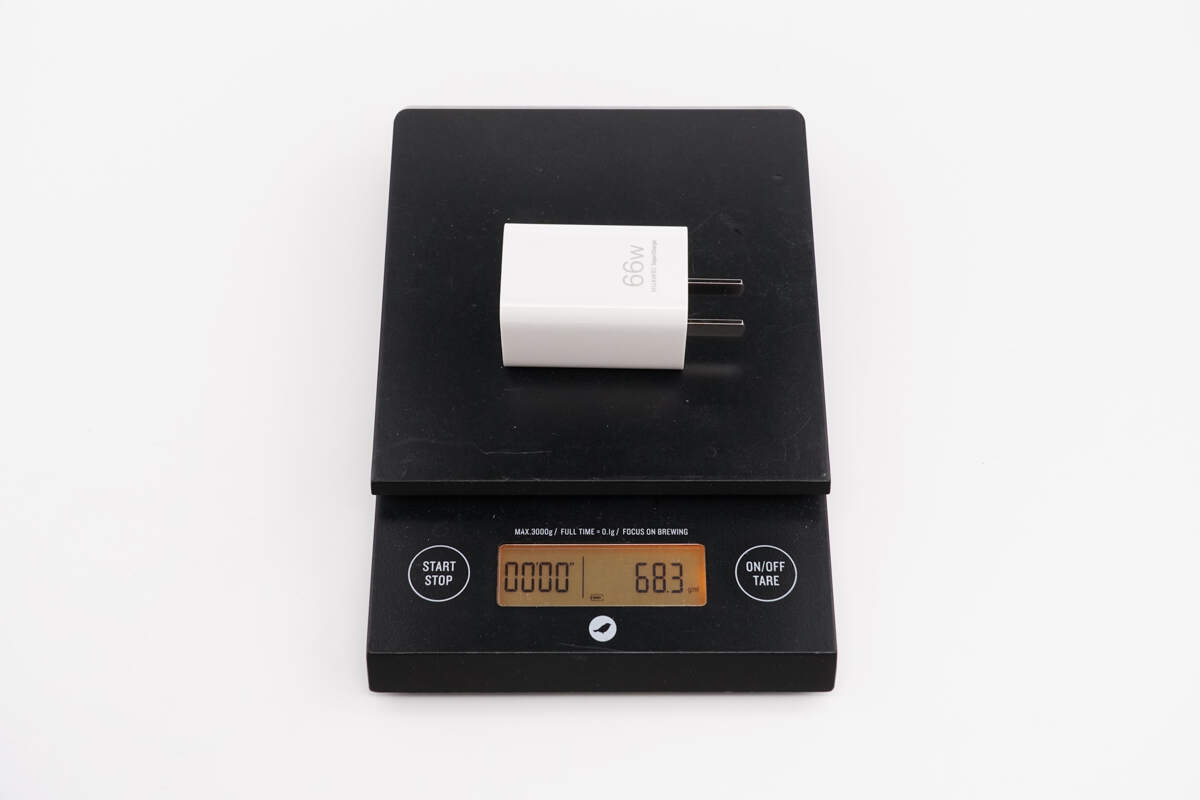
The weight is about 68.3 g (2.41 oz).
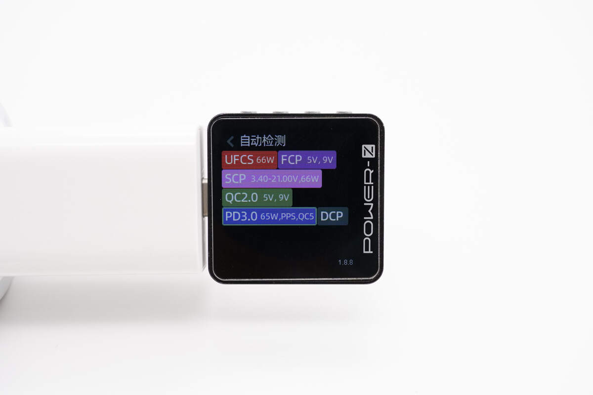
ChargerLAB POWER-Z KM003C shows the USB-C port can support UFCS, FCP, SCP, QC2.0/5, PD3.0, PPS, and DCP charging protocols.
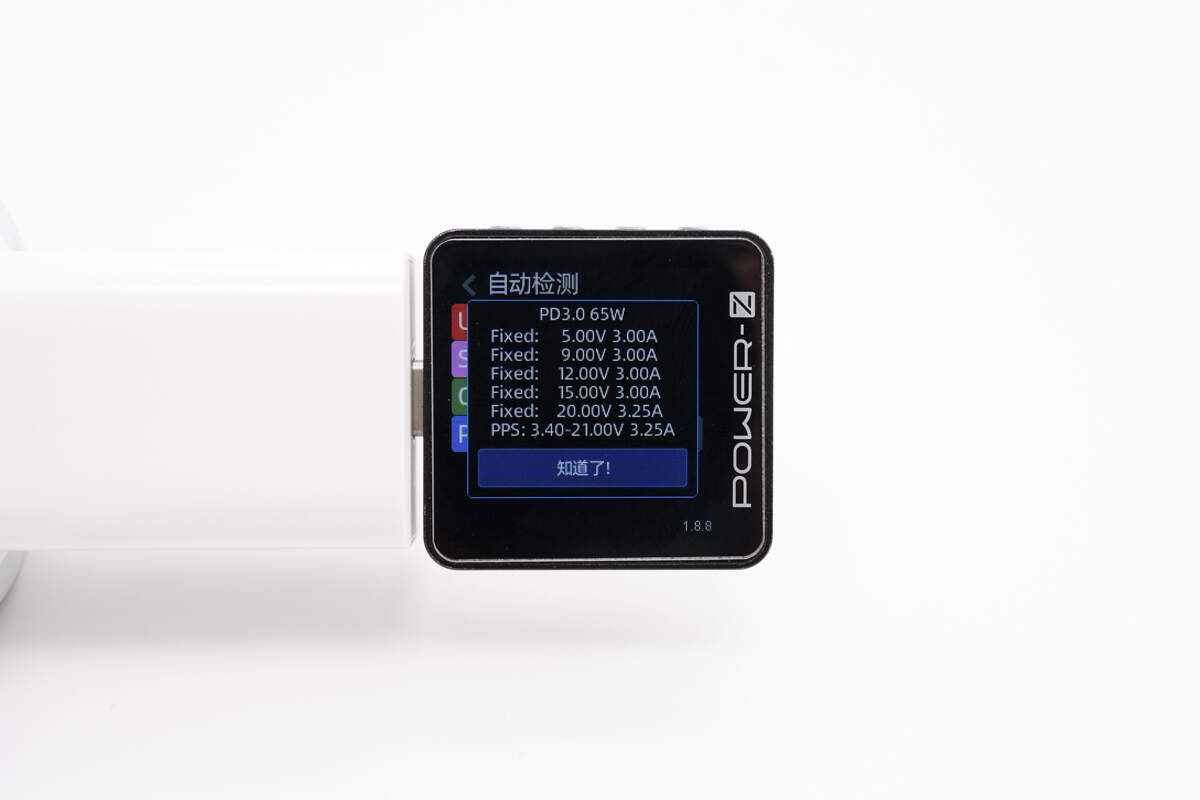
And it has five fixed PDOs of 5V3A, 9V3A, 12V3A, 15V3A, and 20V3.25A. It also has a set of PPS, which is 3.4-21V 3.25A.
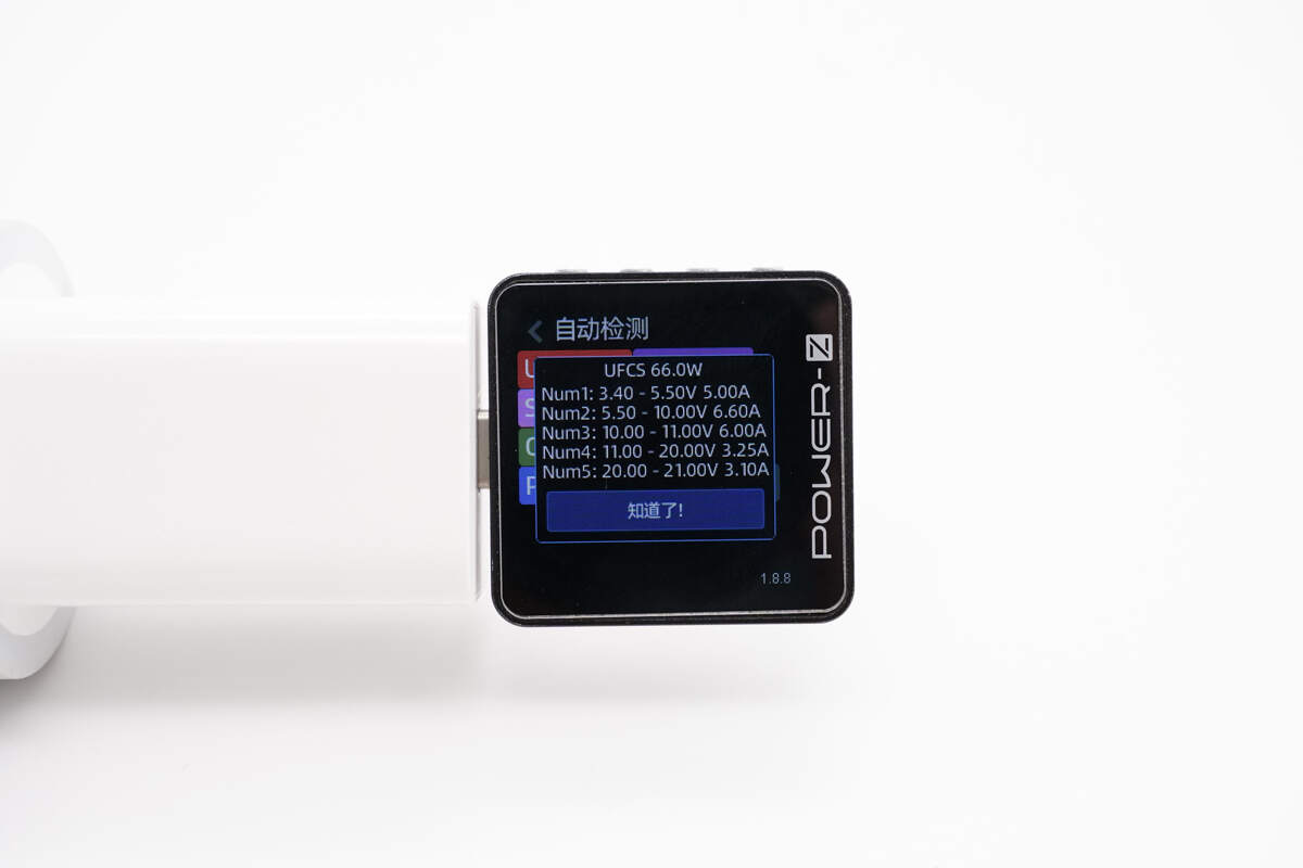
It has five sets of UFCS, which are 3.4-5.5V 5A, 5.5-10V 6.6A, 10-11V 6A, 11-20V 3.25A, and 20-21V 3.1A.
Teardown
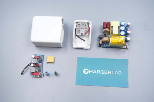
Next, let's take it apart to see its internal components and structure.
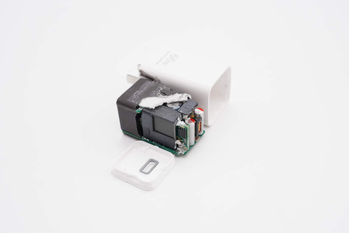
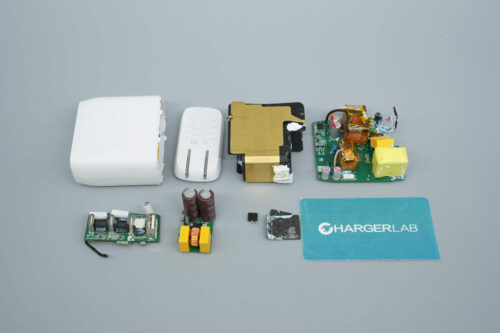
Disassemble the output end cover and take out the PCBA module.
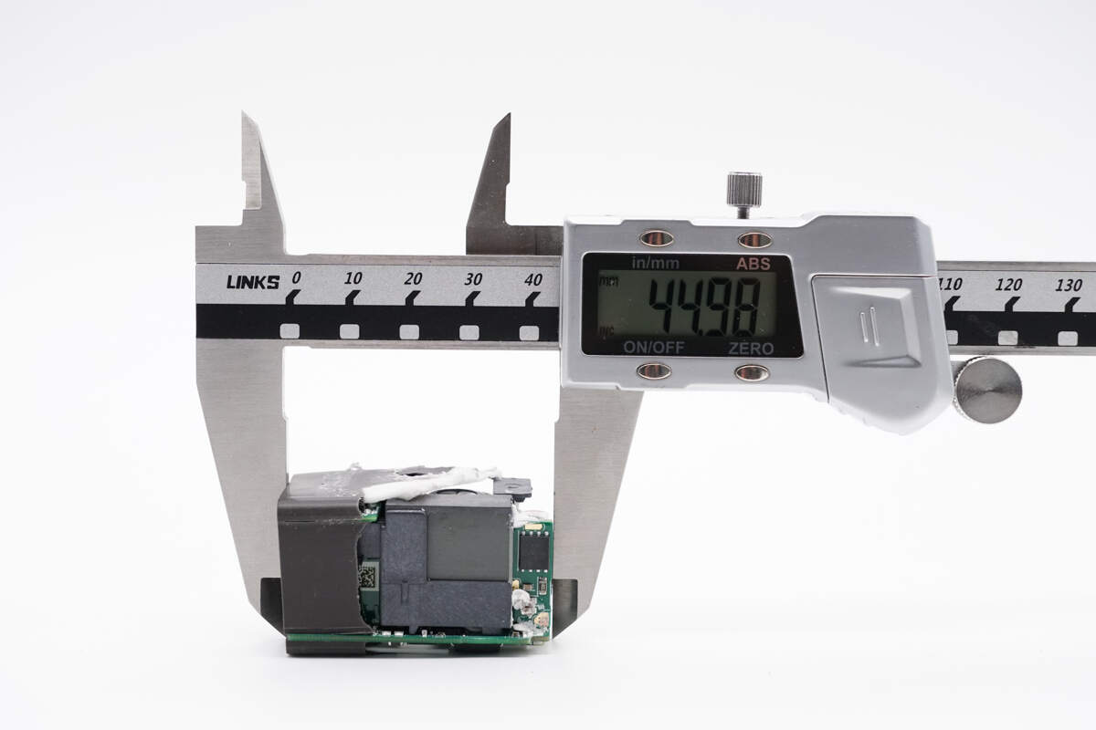
The length of the PCBA module is about 44.98 mm (1.77 inches).
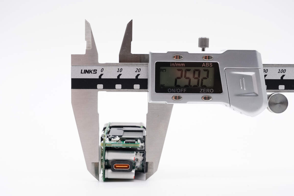
The width is about 25.92 mm (1.02 inches).
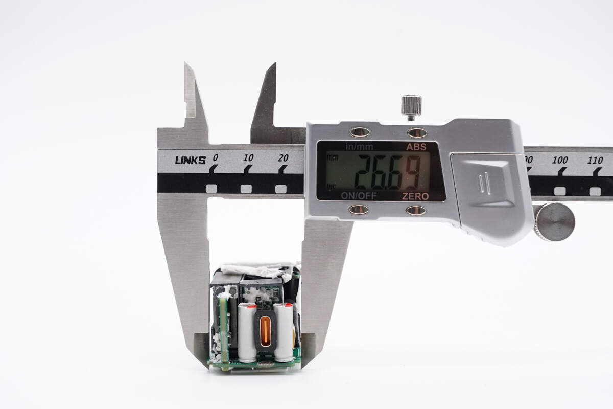
The thickness is about 26.69 mm (1.051 inches).

The input end of the PCBA module is designed for a contact power supply.
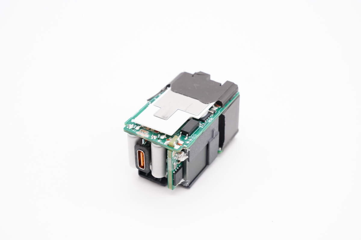
The back side is covered with insulating plates and heat sinks.
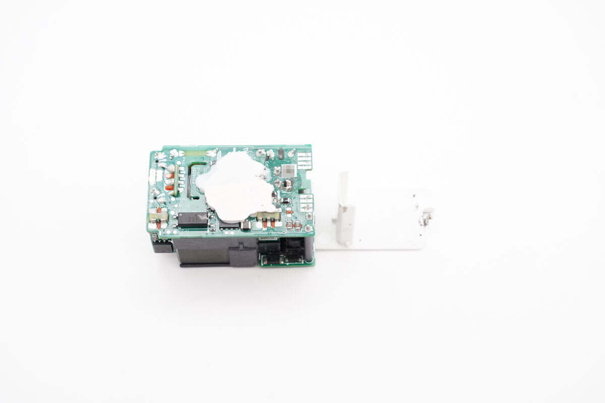
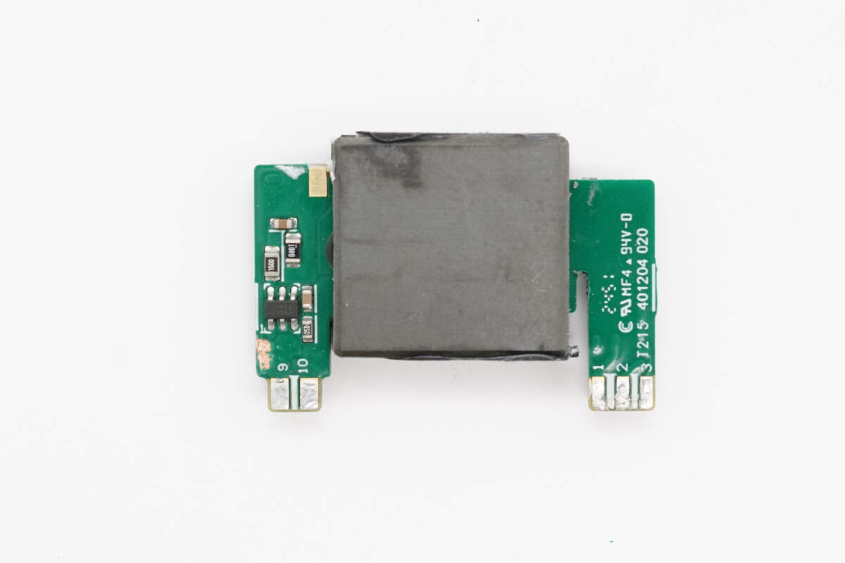
After cleaning off the potting compound, there is a small PCB on the top of the input terminal, which is fixed to the PCBA module through a plastic bracket.
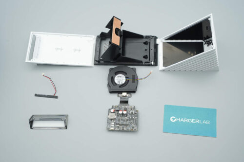
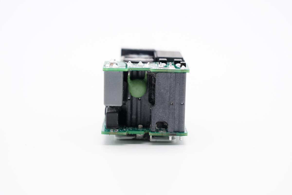
From the side, you can see that there is a small white board between the primary and secondary stages for isolation, which is an integrated design with the plastic board on the back.
There is a planar transformer on the other side, the magnetic core is covered with a plastic shell, and the back of the USB-C socket is also isolated by a plastic shell.
Remove the white plastic plate and use the potting compound on the back of the PCB to help conduct heat.
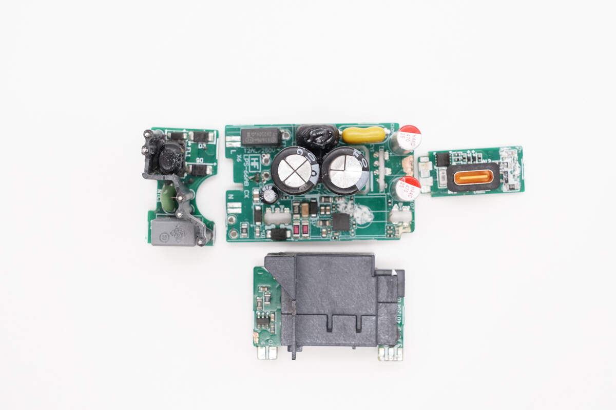
Split the module apart.
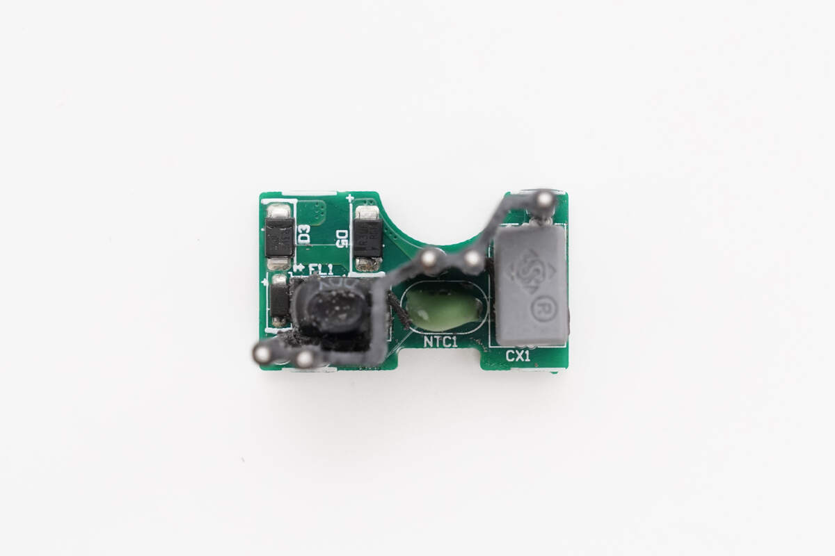
The front of the small PCB at the top of the input end is equipped with an NTC thermistor, a safety X capacitor, a common mode choke, and two rectifiers.
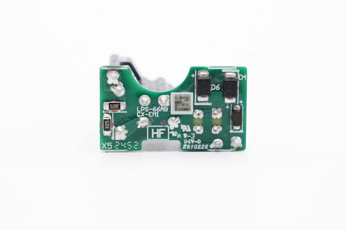
The other two rectifiers are on the back, and four of them form a bridge rectifier.
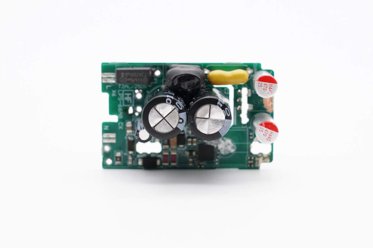
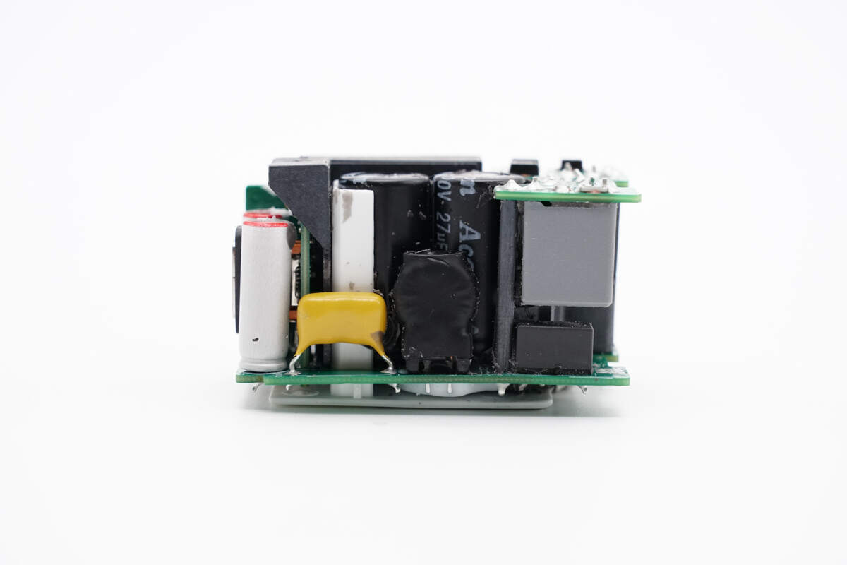
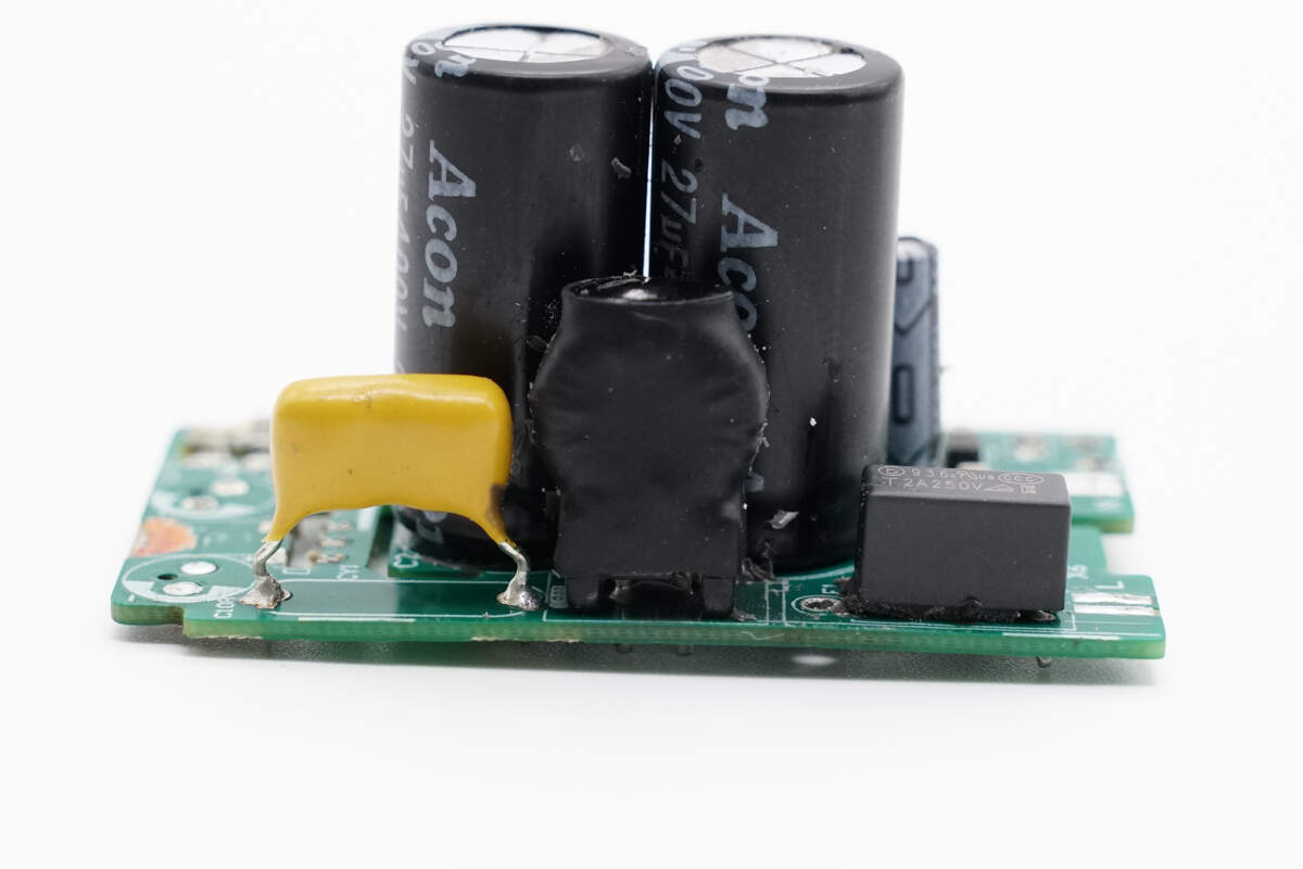
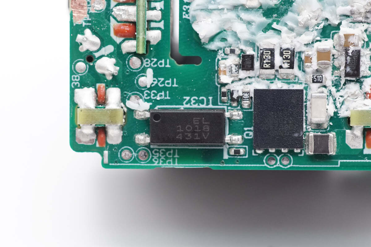
There is a time delay fuse, an electrolytic capacitor, a filter inductor, a master control chip, a safety Y capacitor, and a solid capacitor on the front of the PCBA.
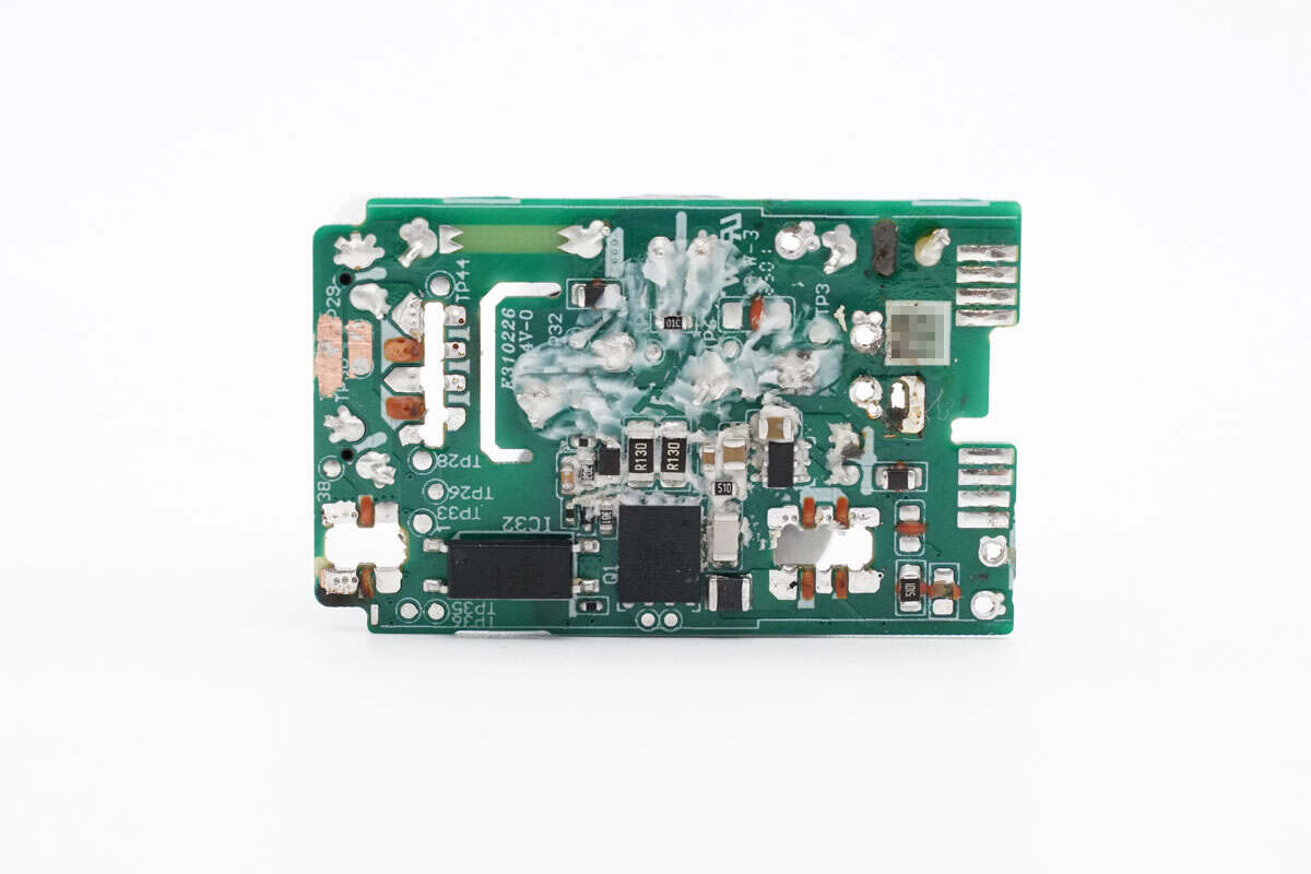
The back is equipped with a primary MOSFET, an optocoupler, and other components.
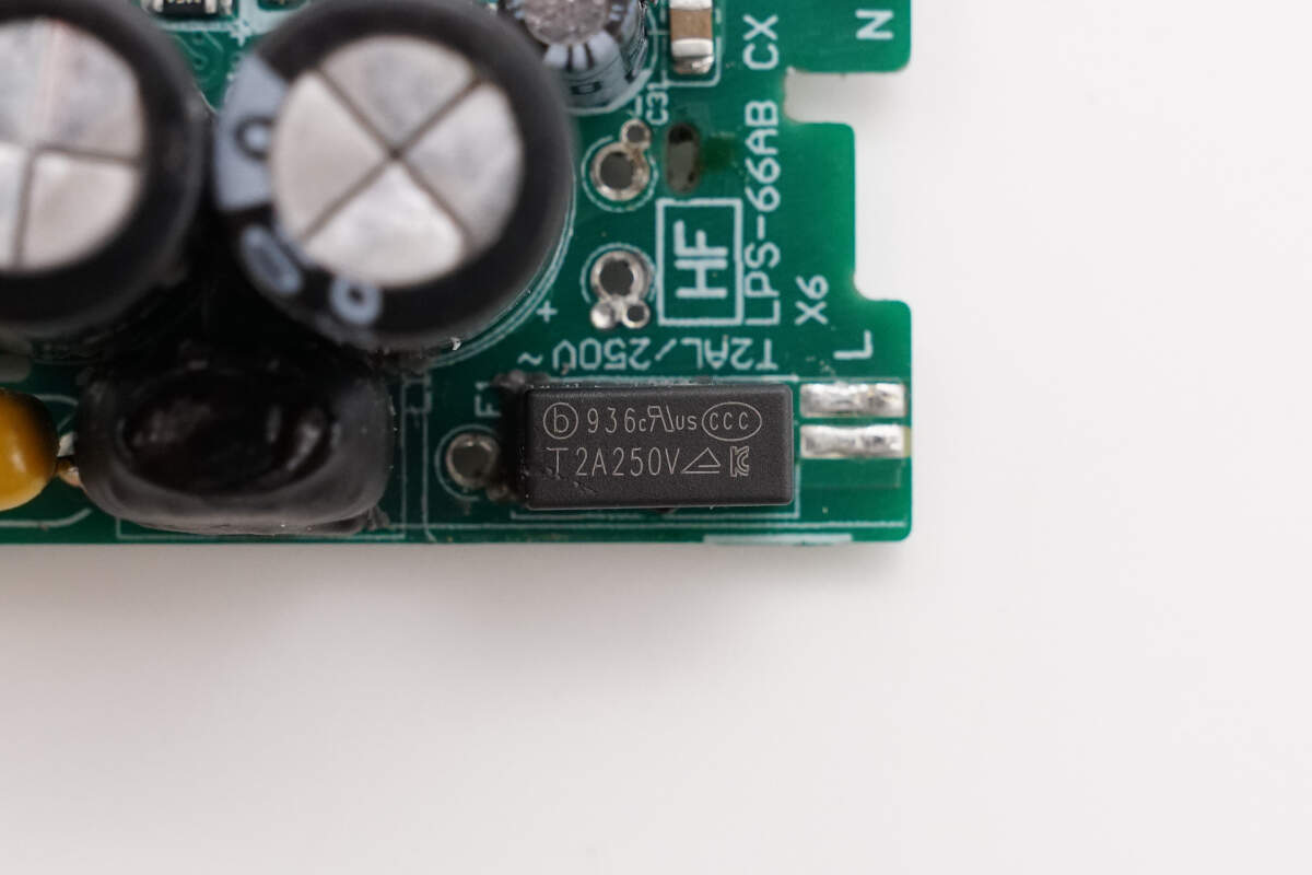
The time delay fuse is from Betterfuse. 2A 250V.
The NTC thermistor is used to suppress the power-on surge current.
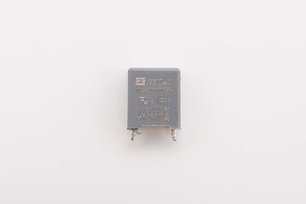
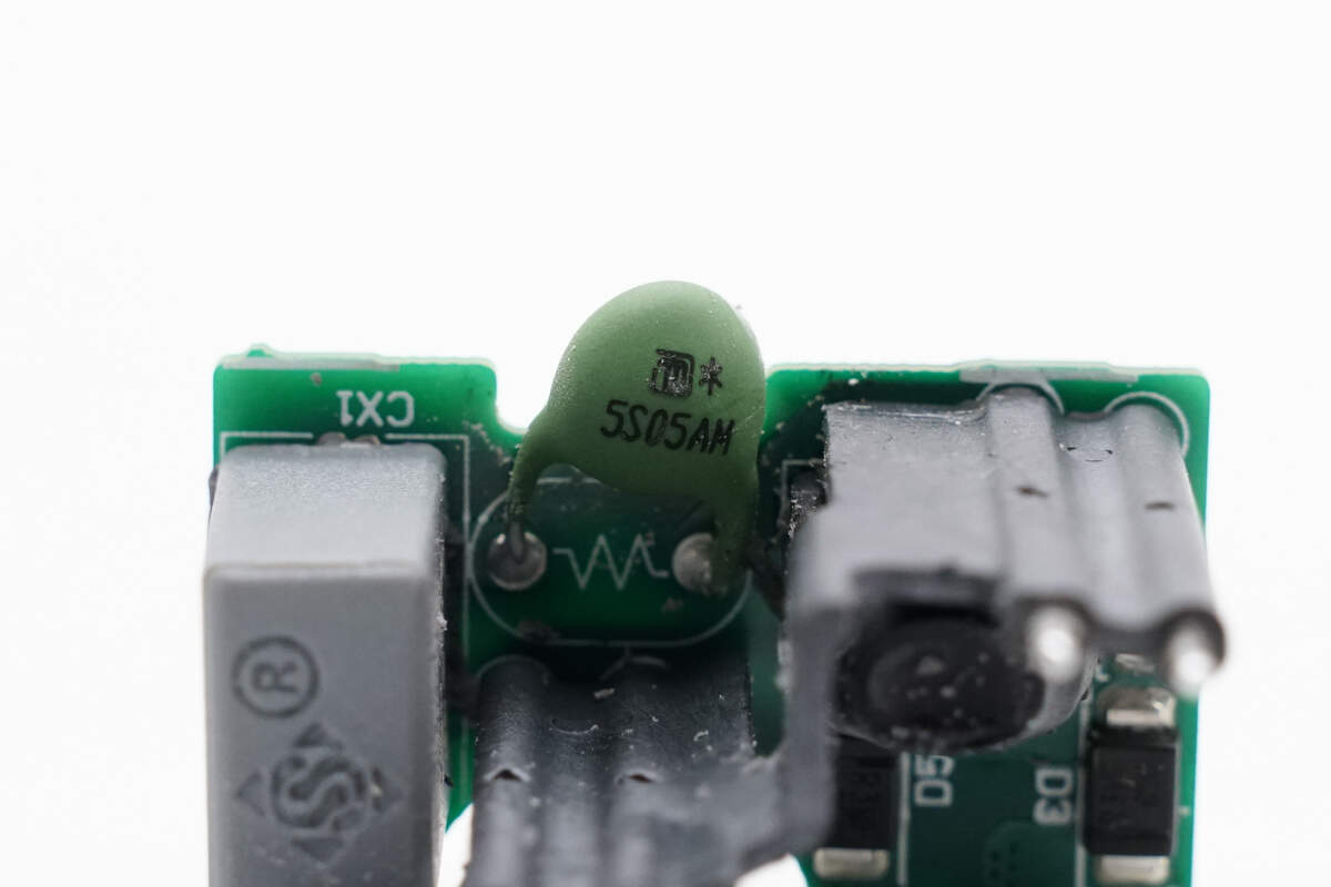
The safety X2 capacitor is from STE. 0.1μF.
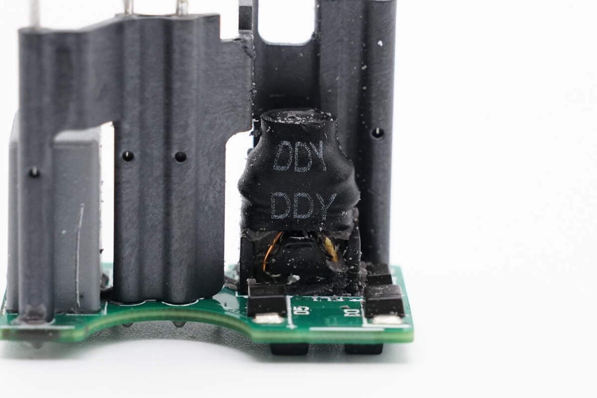
The common mode choke is used to filter out EMI interference and is insulated by heat-shrinkable tubing.
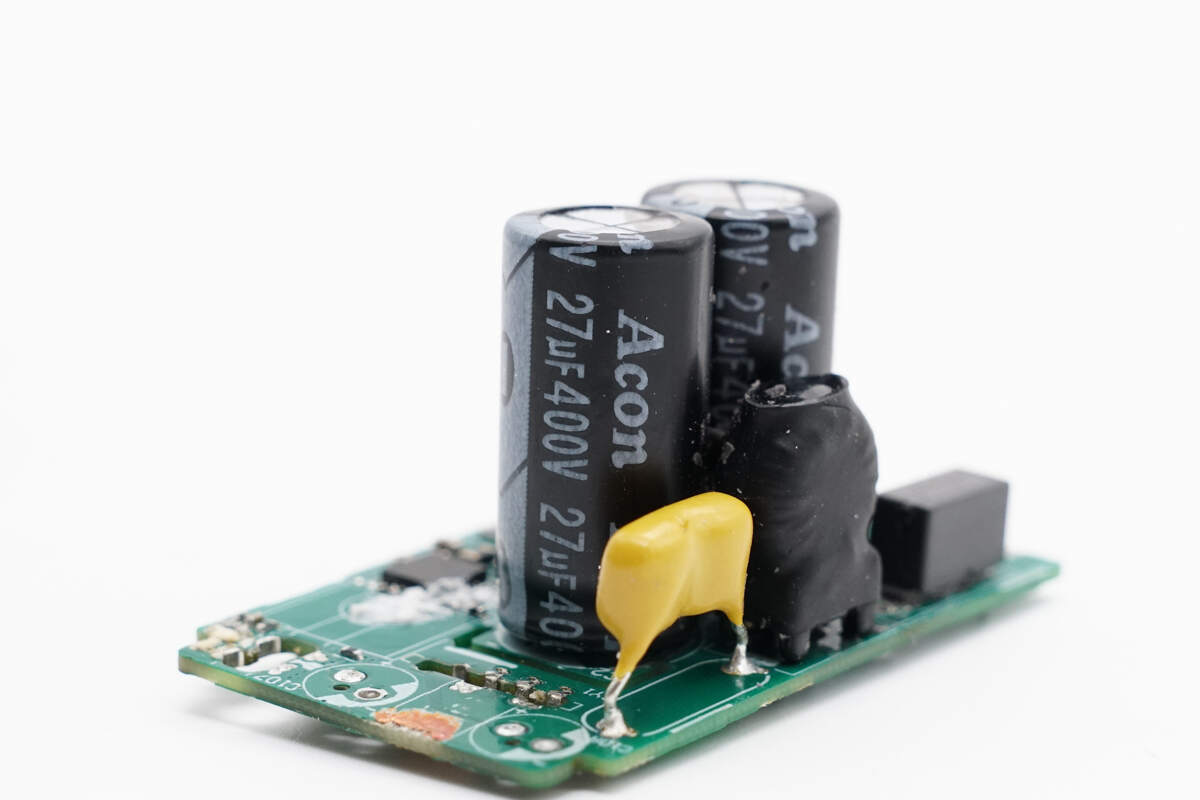
The two electrolytic capacitors are from Acon. 400V 27μF.
The filter inductor is insulated by heat-shrinkable tubing.
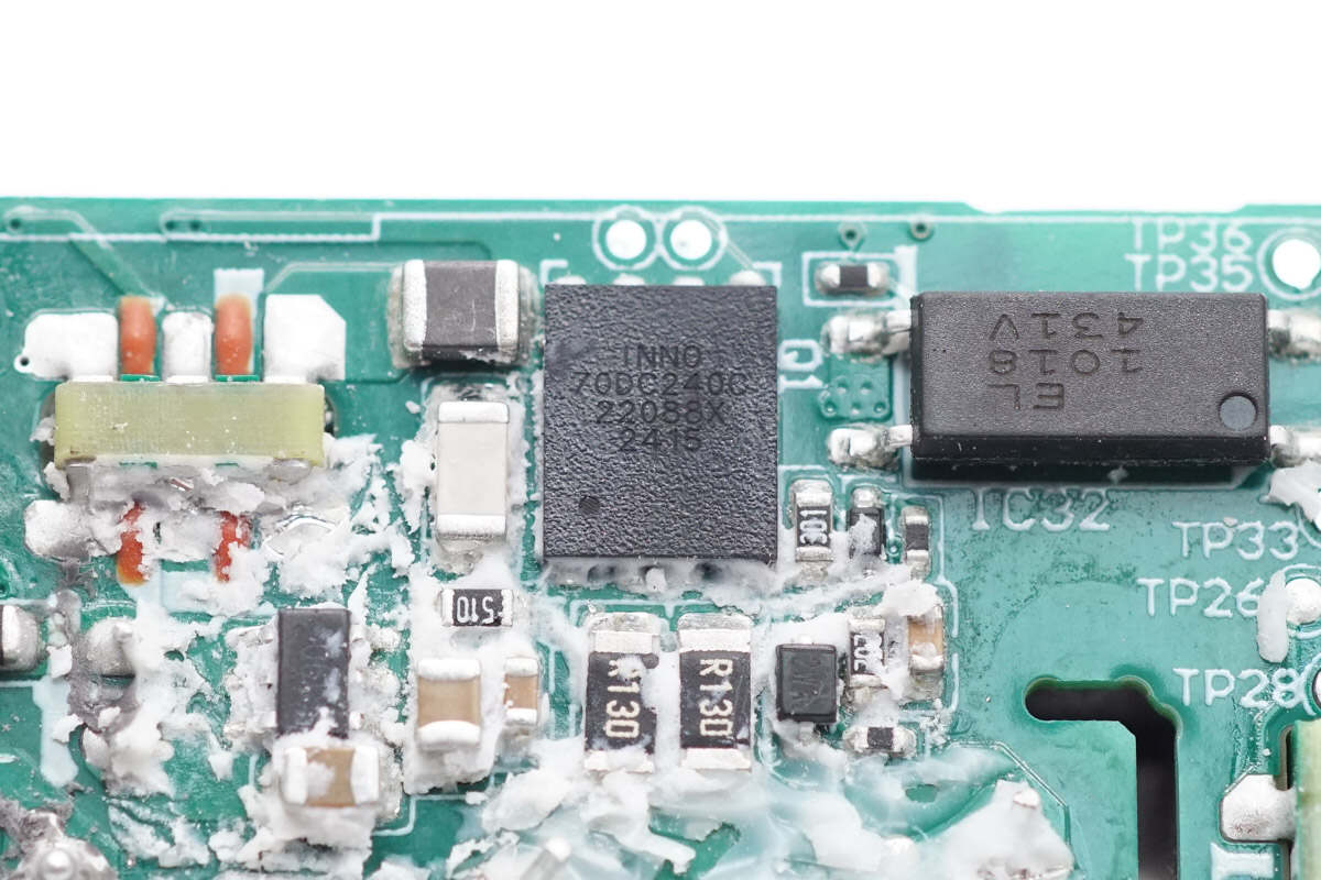
The primary MOSFET is from Innoscience and adopts the DFN5*6 package. Withstand voltage 700V, conduction resistance 240mΩ, meets JEDEC standard industrial application requirements, built-in ESD protection. Model is INN700DC240C.
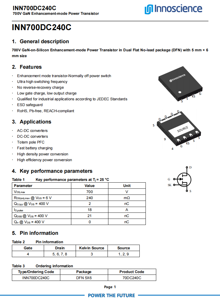
Here is the information about the Innoscience INN700DC240C.
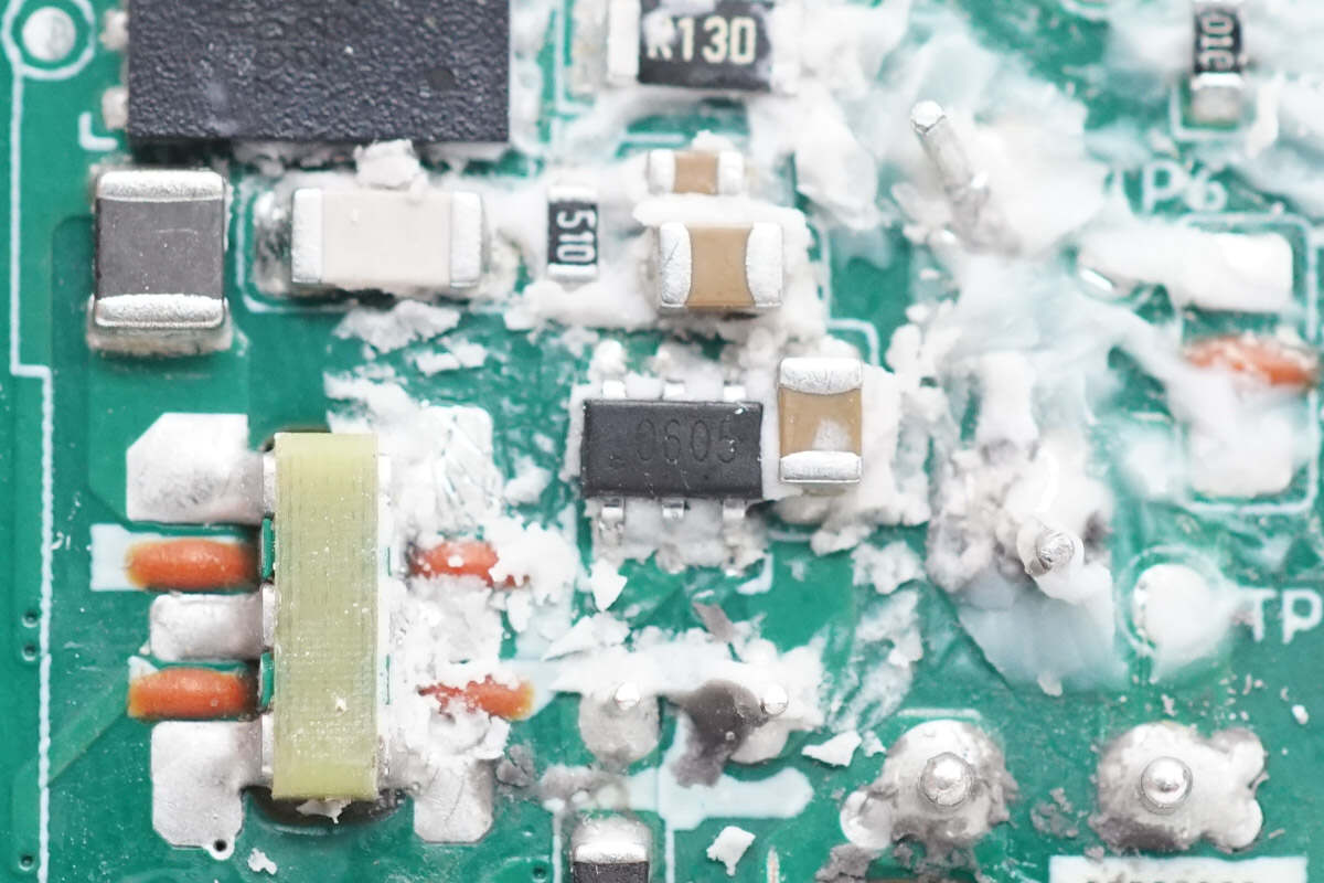
The auxiliary MOSFET is marked with 0605.
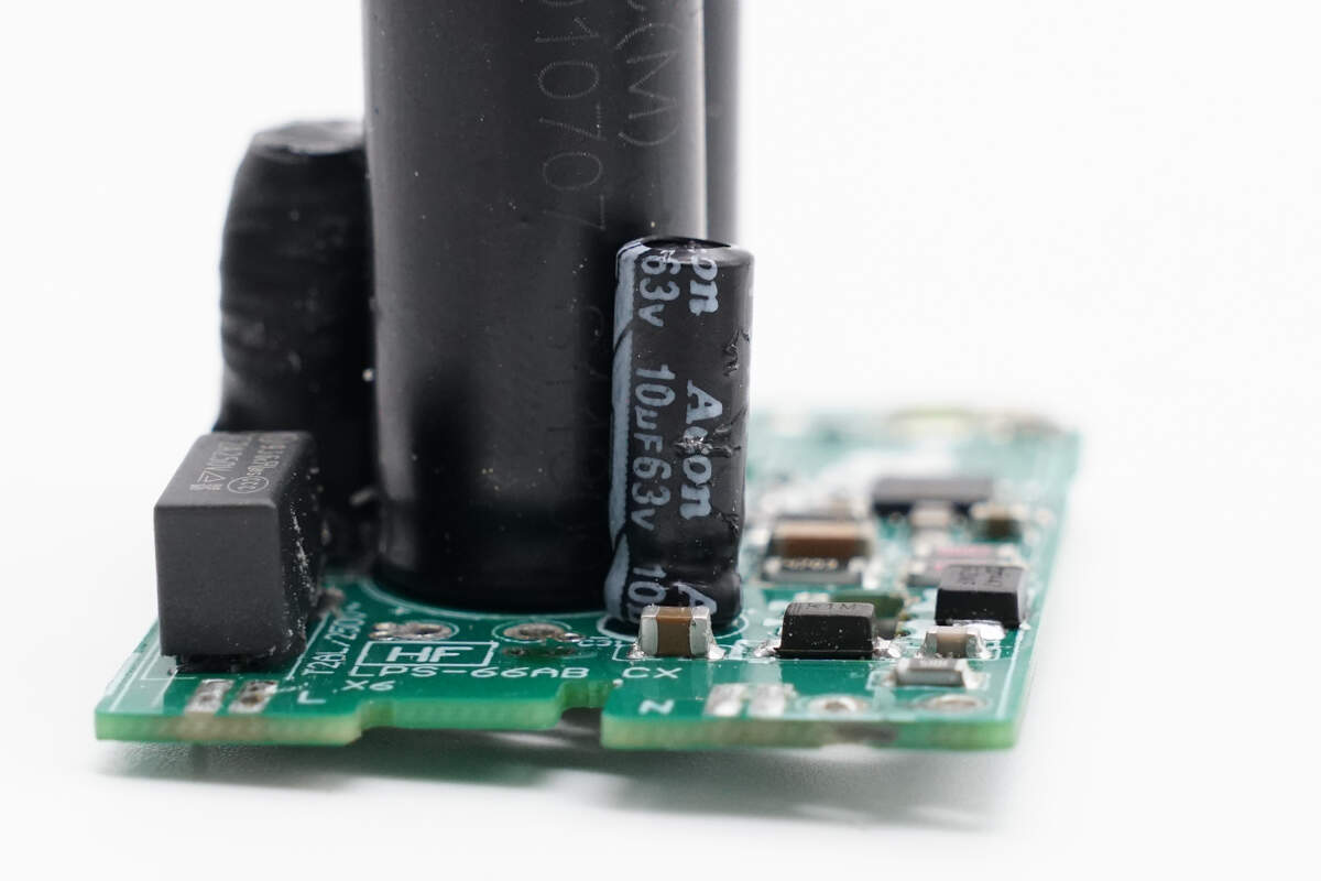
The capacitor that powers the master control chip is also from Acon. 63V 10μF.
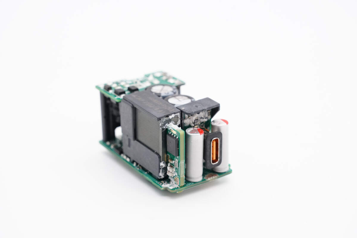
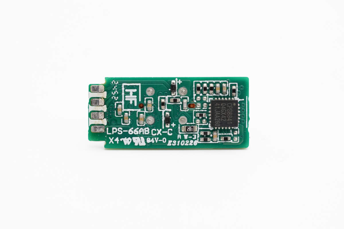
The magnetic core of the planar transformer is protected by a plastic shell, and there is a synchronous rectifier controller on the left side of the PCB.
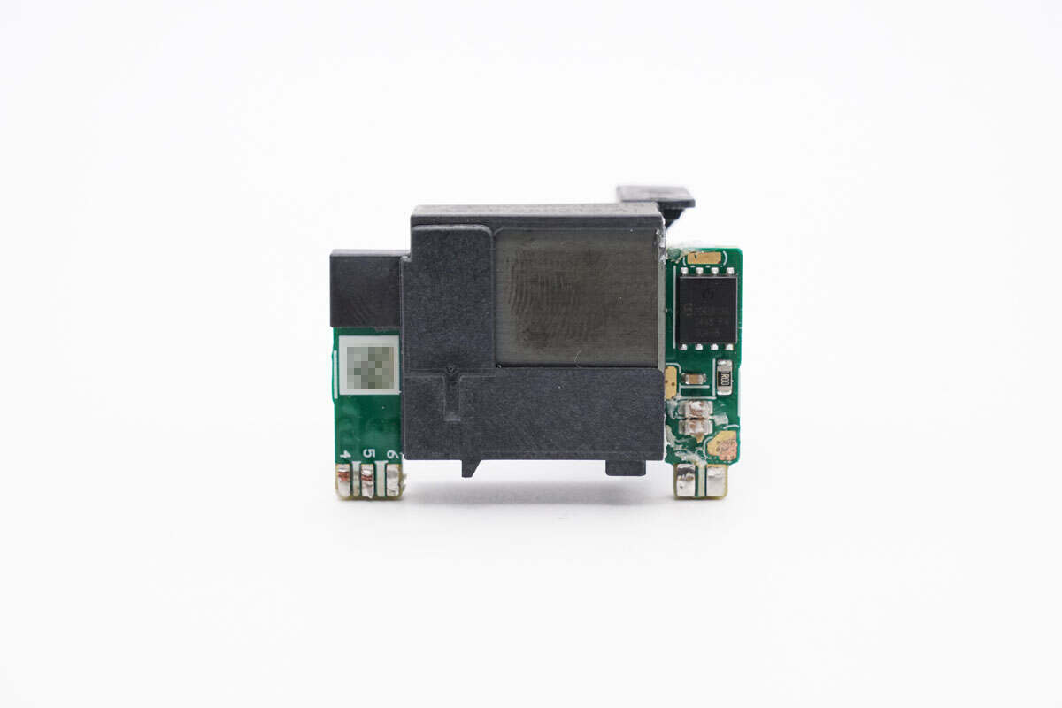
There is a synchronous rectifier on the back.
Remove the plastic shell.
The optocoupler is from Everlight and is used for output voltage feedback.
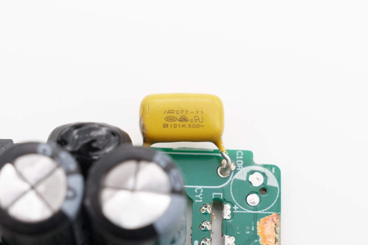
The safety Y capacitor is from Fenghua Advanced. It is a CT7 series Y capacitor.
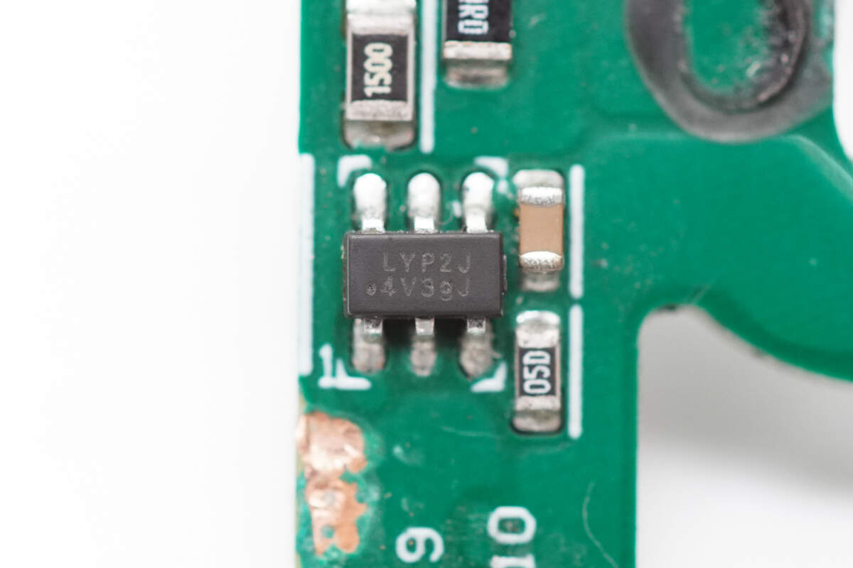
The synchronous rectifier controller is marked with LYP2J.
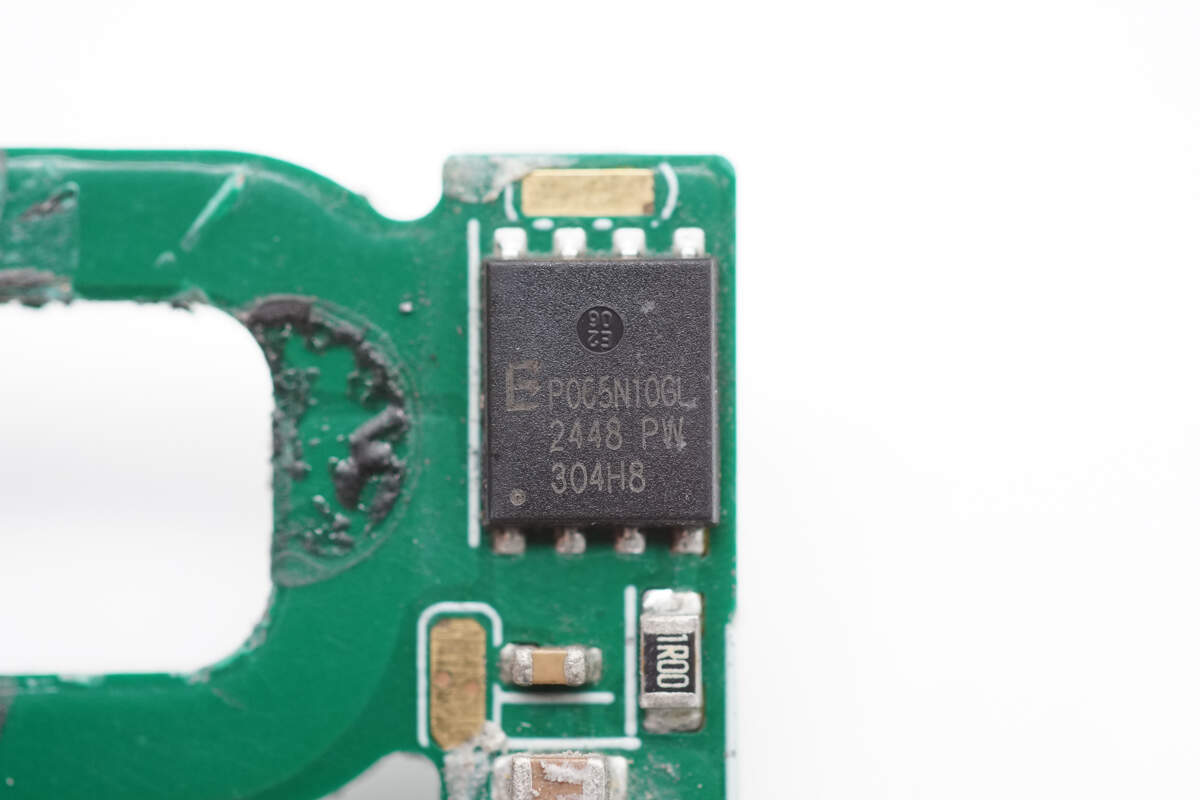
The synchronous rectifier is from Belling and adopts the PDFN5*6 package. 100V 6mΩ. Model is BLP065N10GL.
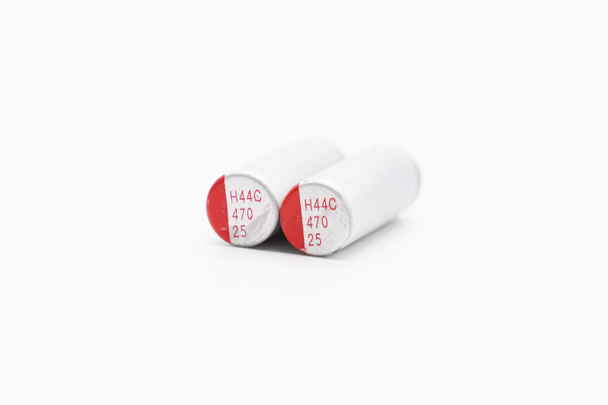
There are two solid capacitors for output filtering. 25V 470μF.
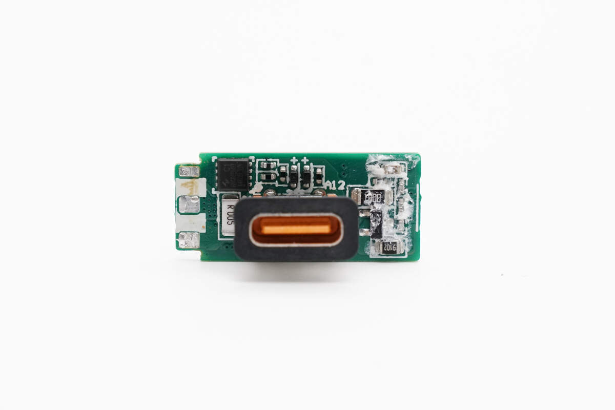
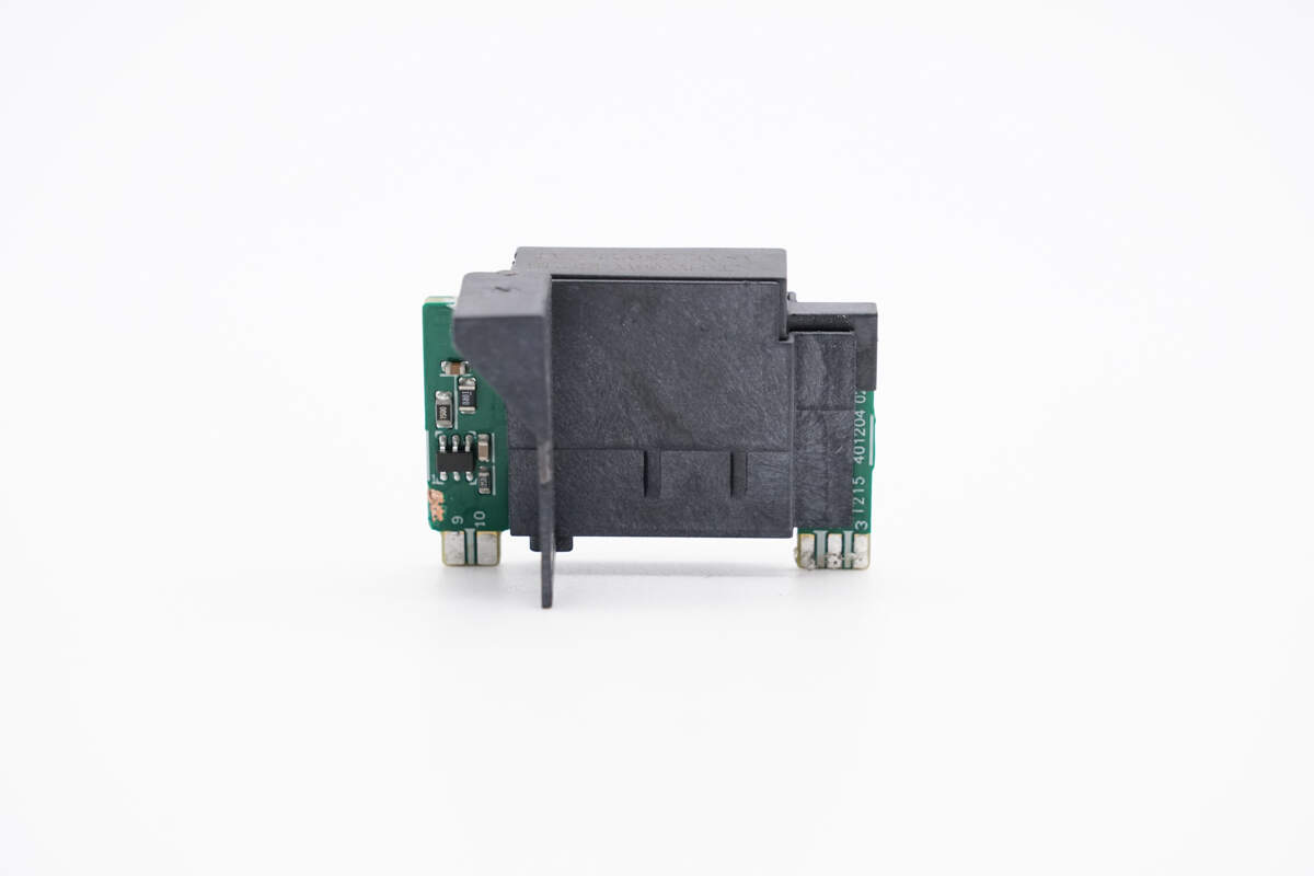
There is a USB-C female socket and an output VBUS MOSFET on the small PCB at the output end.
There is a protocol chip on the back.
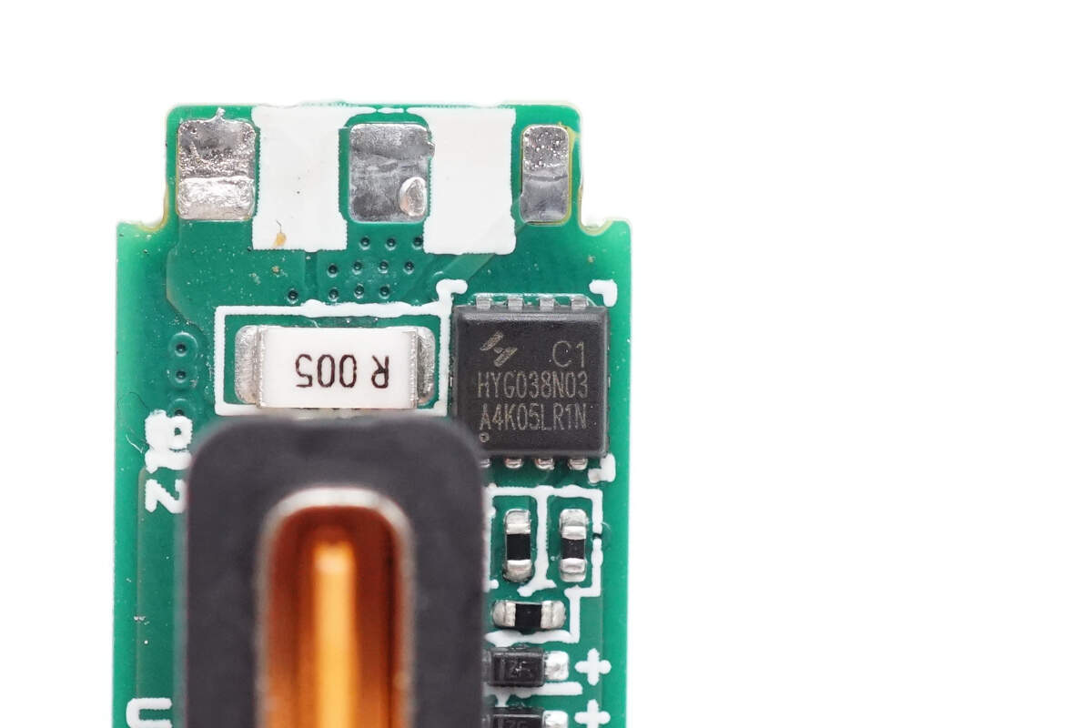
The output VBUS MOSFET is from Huayi and adopts the PDFN 8L package. 30V 3.1mΩ. Model is HYG038N03LR1C1.
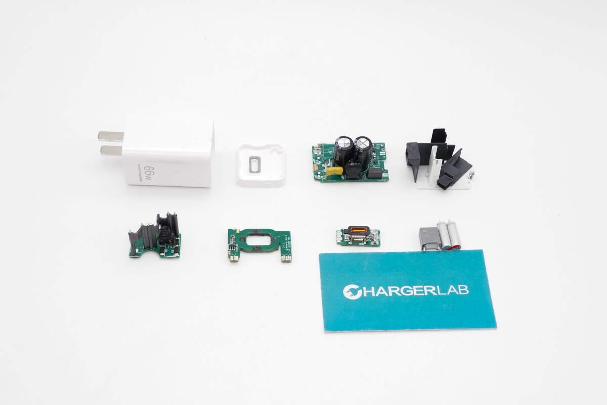
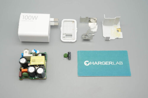
Well, those are all components of the Huawei Pura X Original 66W GaN Charger.
Summary of ChargerLAB
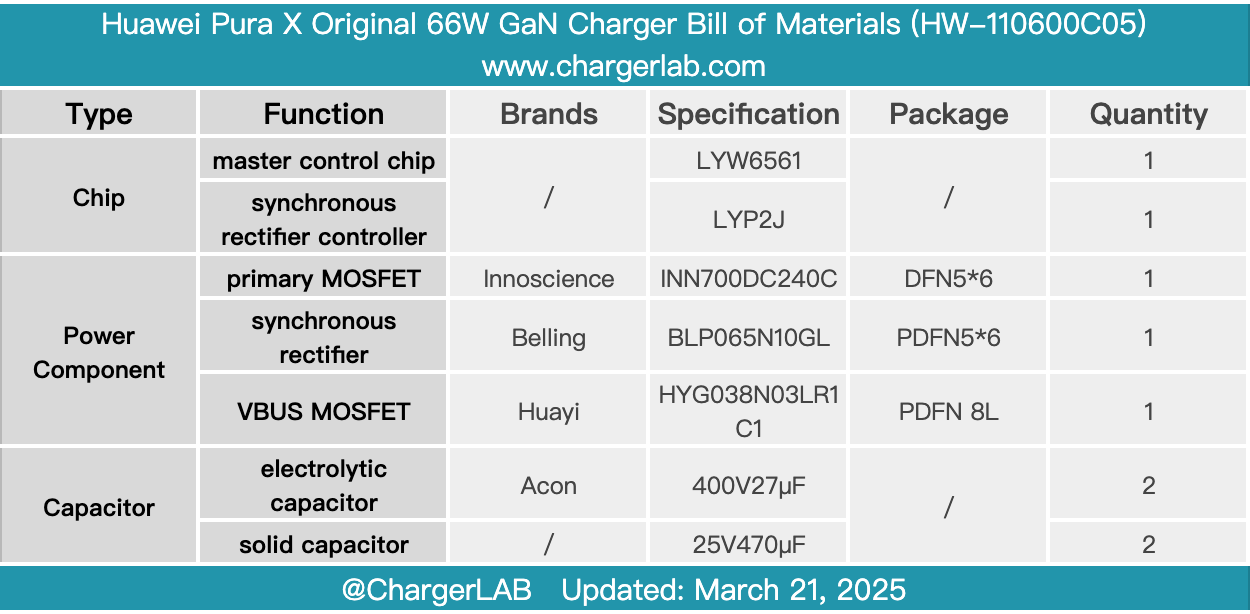
Here is the component list of the Huawei Pura X Original 66W GaN Charger for your convenience.
It is small and exquisite, very convenient to carry. It not only supports 66W Huawei Super Fast Charge but also supports 65W PD and UFCS, meeting the fast charging needs of different brands of phones, laptops, tablets, watches, headphones, game consoles, and other devices.
After taking it apart, we found that its internal PCBA module adopts a design of stacking multiple small PCBs, and is equipped with plastic brackets, shells, isolation plates, etc., which not only provides good protection, but also makes the module more stable and reliable as a whole. Its internal structure is stable and reliable, and the space utilization is compact and reasonable.
Related Articles:
1. Teardown of ANKER 253W GaN Power Adapter
2. Teardown of ANKER 150W 4 USB-C Ports GaN Charger
3. Teardown of Motorola 50W Charger