Introduction
The device being disassembled in this session is the Huawei P30 smartphone. Released in 2019, it features a 6.1-inch OLED waterdrop display with a resolution of 2340 × 1080 pixels and supports in-display fingerprint recognition. It is powered by the Kirin 980 octa-core processor, paired with 8GB of RAM and up to 256GB of internal storage.
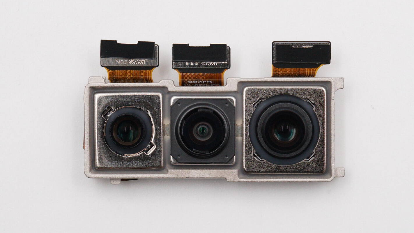
The phone is equipped with a 40-megapixel main camera, a 16-megapixel ultra-wide camera, and an 8-megapixel telephoto lens, while the front-facing camera has a resolution of 32 megapixels. It houses a 3650mAh battery with support for 22.5W fast charging. Below, we'll provide a full teardown of the Huawei P30, showcasing the internal design and material quality.
Product Appearance
The display measures 6.1 inches with a resolution of 2340 × 1080 pixels and features a front-facing camera at the top.
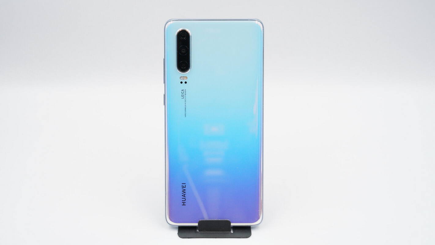
On the back, it is equipped with a 40-megapixel main camera, a 16-megapixel ultra-wide camera, and an 8-megapixel telephoto lens, with a fill light and laser sensor positioned below.
The left side of the device houses the SIM card slot.
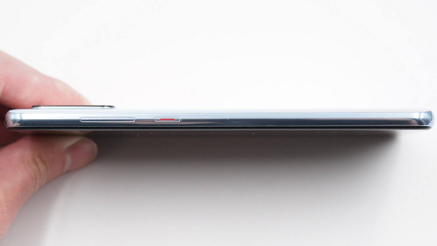
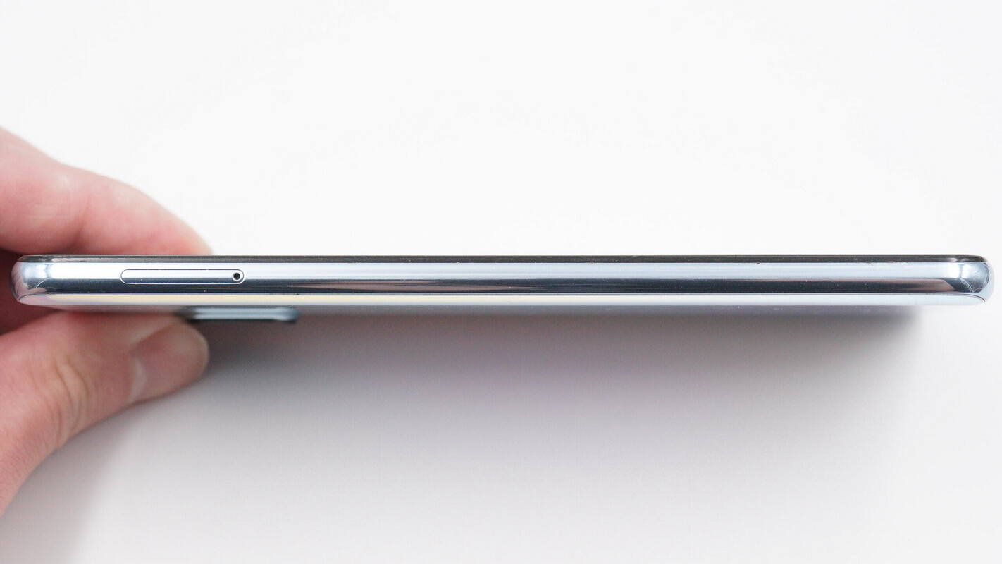
The right side of the device features the volume buttons and the power button.
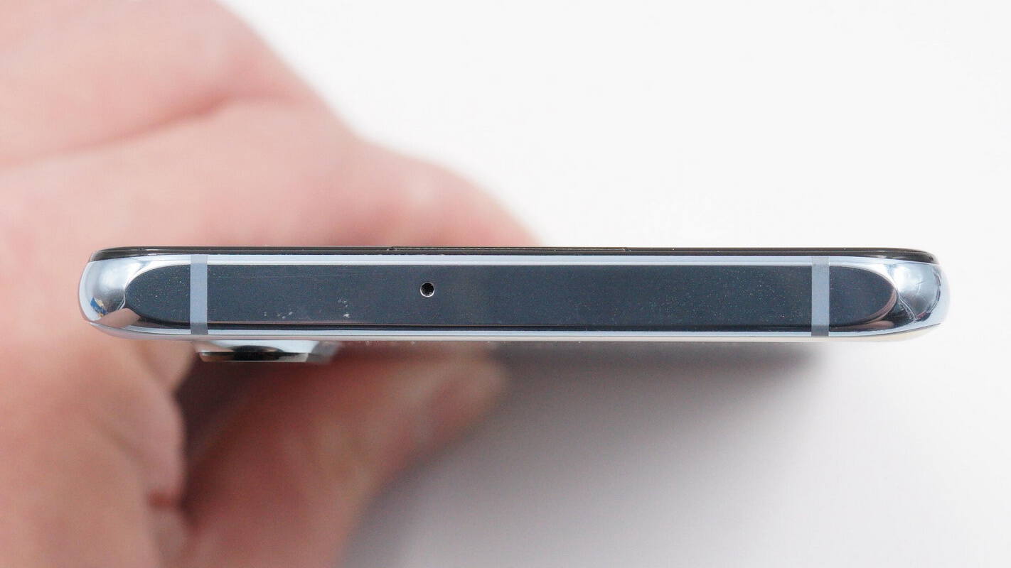
The top of the device is equipped with a microphone opening.
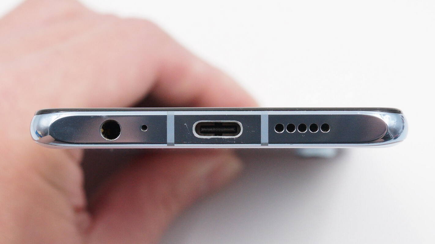
The bottom of the device features a 3.5mm headphone jack, a microphone opening, a USB-C port, and a speaker grille.
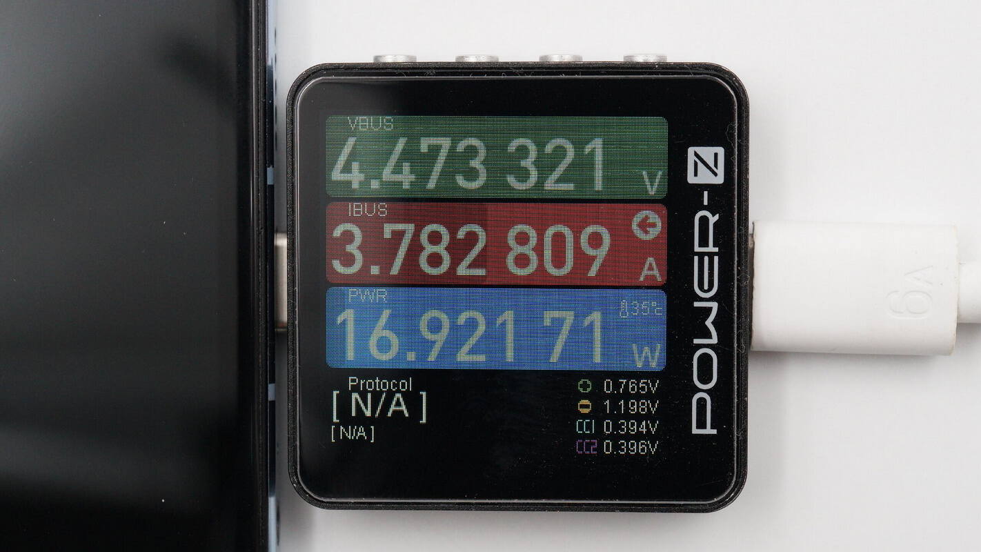
ChargerLAB POWER-Z KM003C shows the charging voltage is about 4.47 V, the charging current is about 3.78 A, resulting in a charging power of about 17 W.
Teardown
Next, let's take it apart to see its internal components and structure.
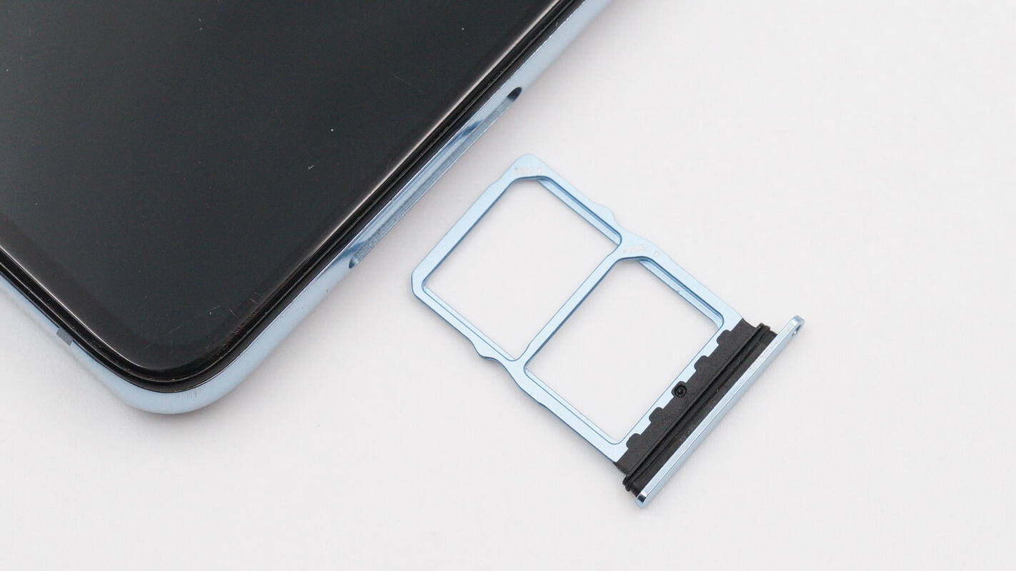
Remove the SIM tray, revealing a sealing gasket.
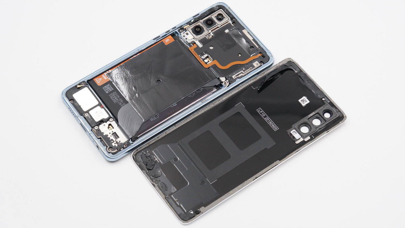
Cut through the adhesive along the edges, and remove the back cover.
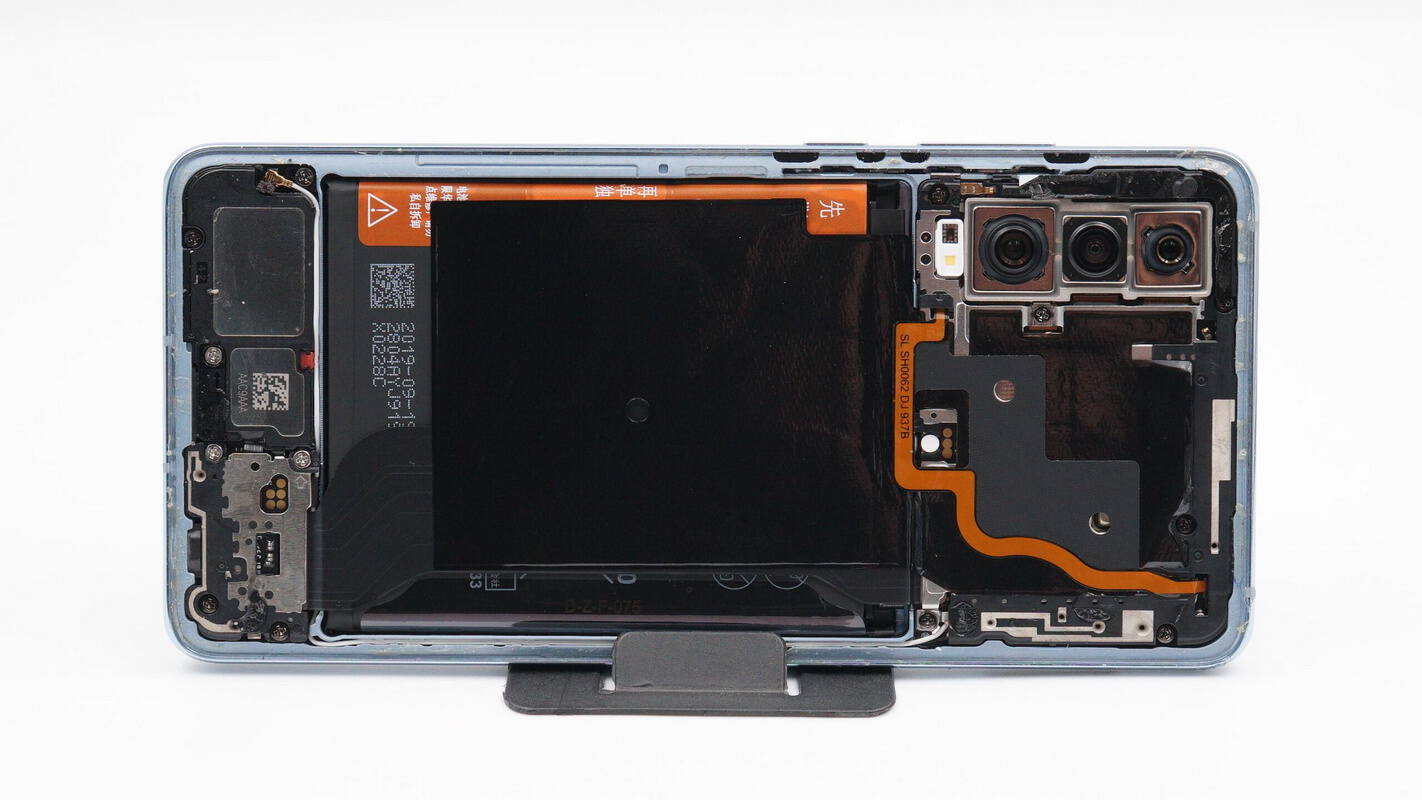
The mainboard and daughterboard are secured with plastic clamps and screws. Above the battery, there are connecting flex cables and a graphite thermal pad.
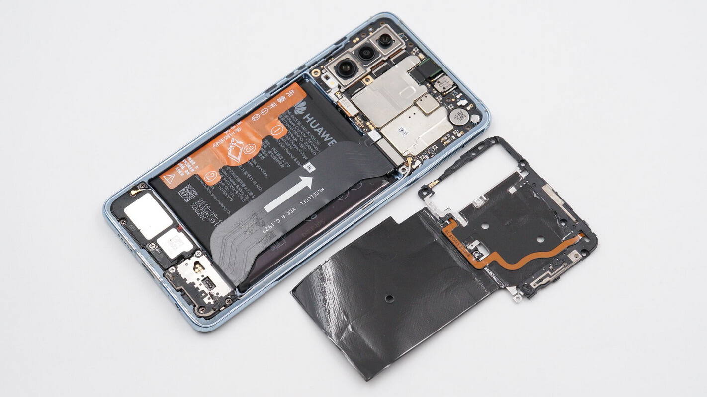
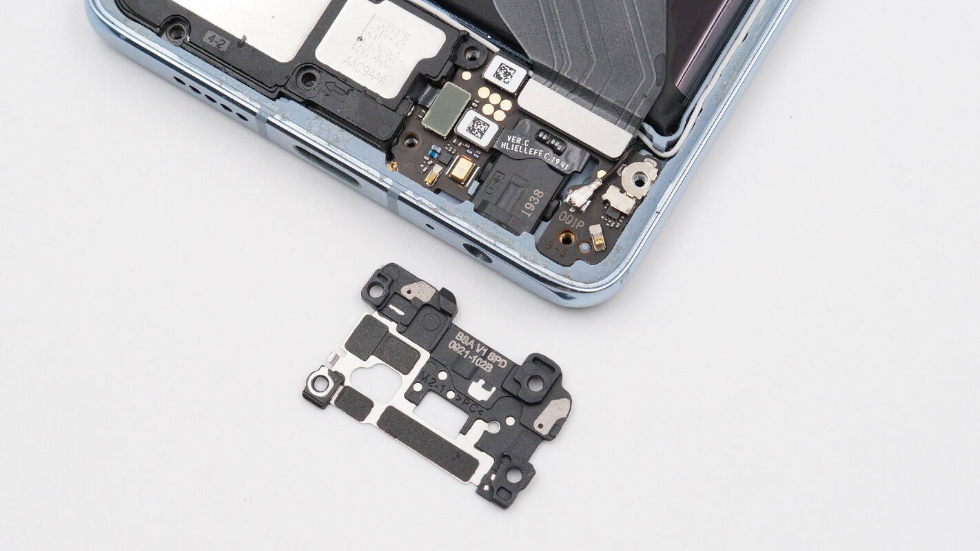
Unscrew the screws and remove the plastic clamp on the mainboard.
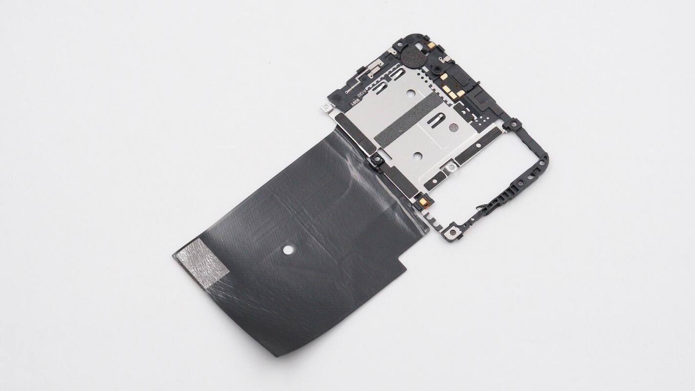
On the inner side of the plastic clamp, there is a metal plate with antennas along the edges, and a graphite thermal pad is attached.
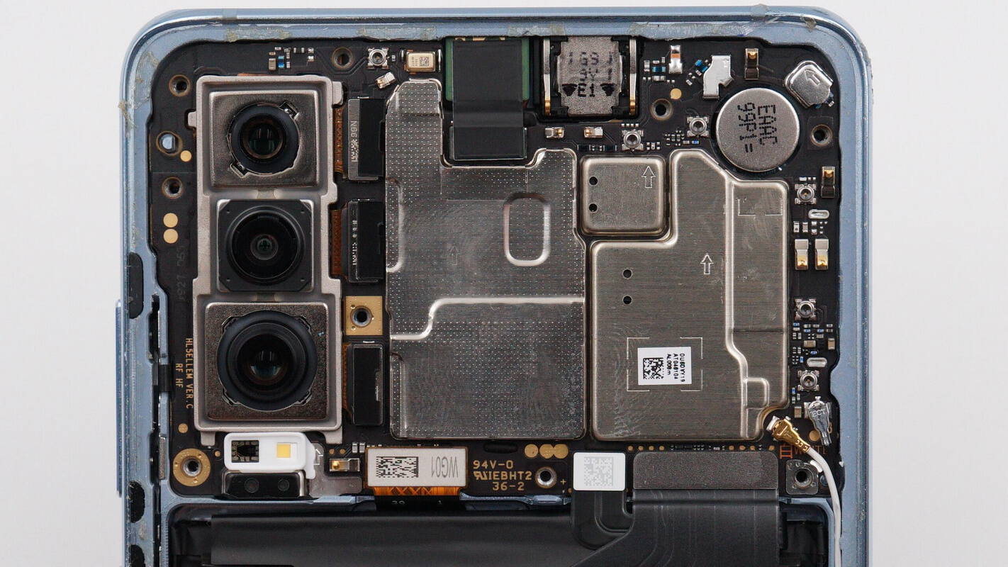
The camera, display, and USB-C PCB are all connected to the mainboard via connectors.
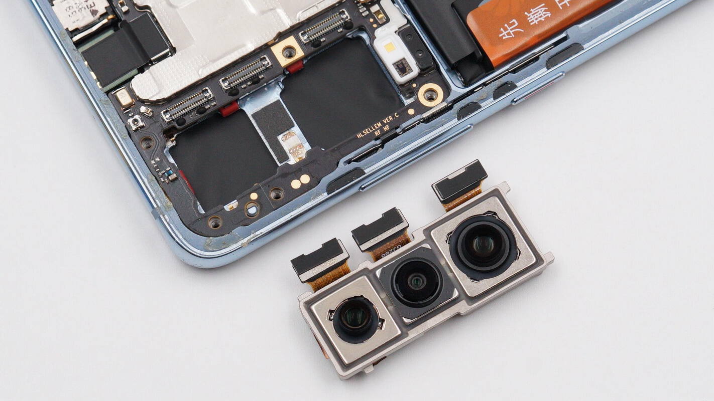
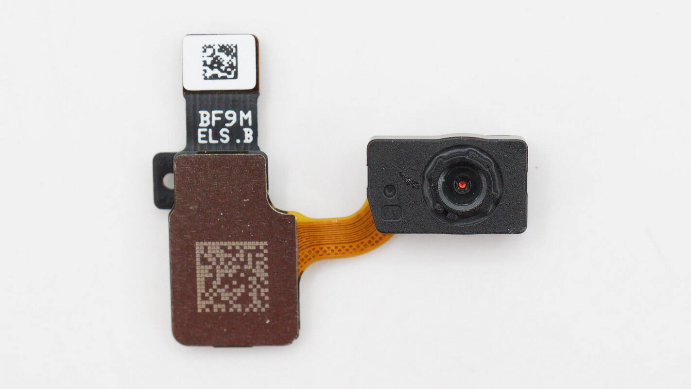
Open the connector and remove the cameras.
The cameras are secured inside the anti-roll frame using adhesive.
Remove the clamp on the daughterboard.
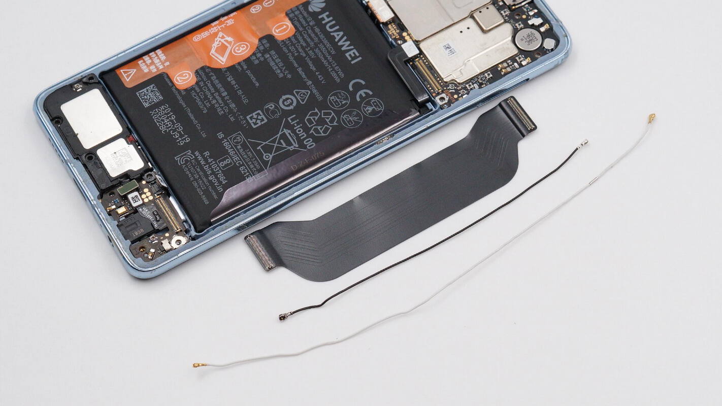
Disconnect the flex cable and coaxial signal cables.
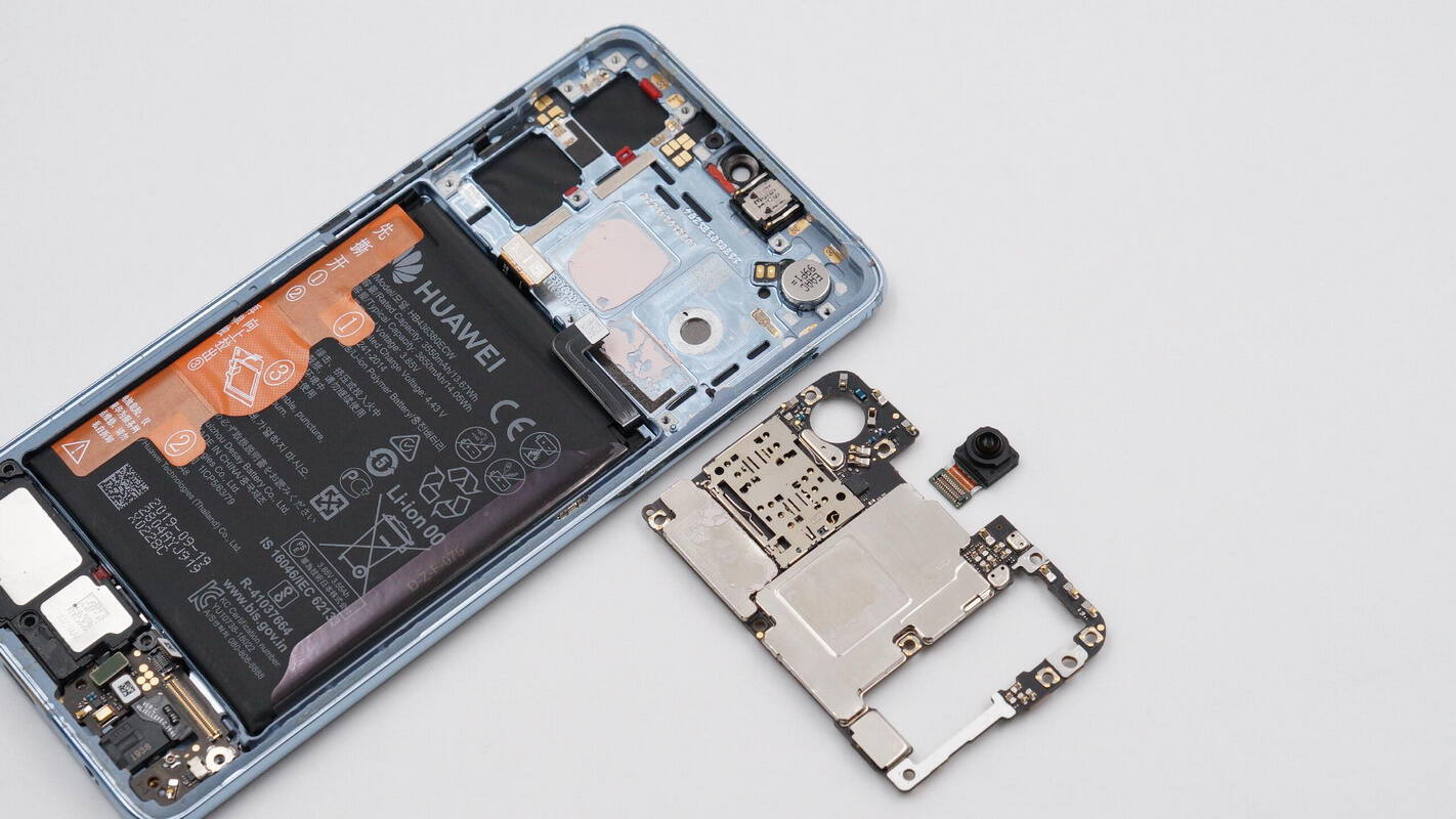
Remove the front-facing camera and the mainboard.
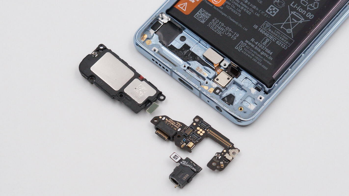
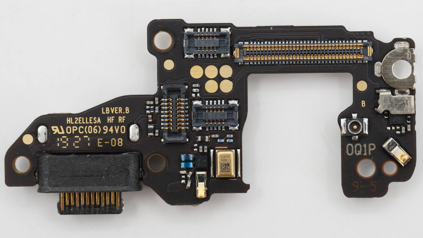
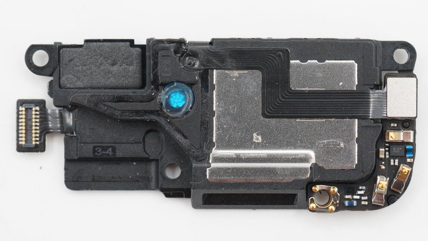
Remove the daughterboard, the headphone jack, and the speaker.
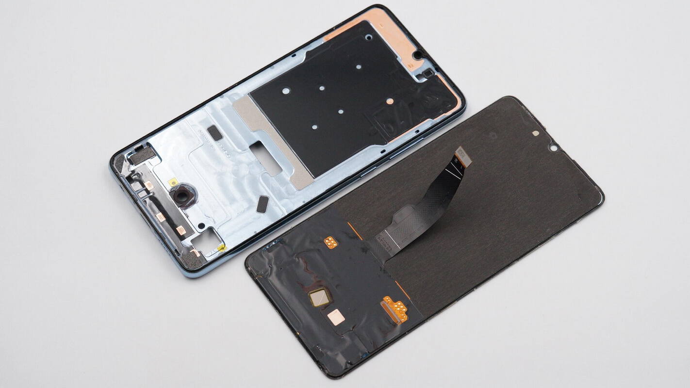
Remove the OLED display.
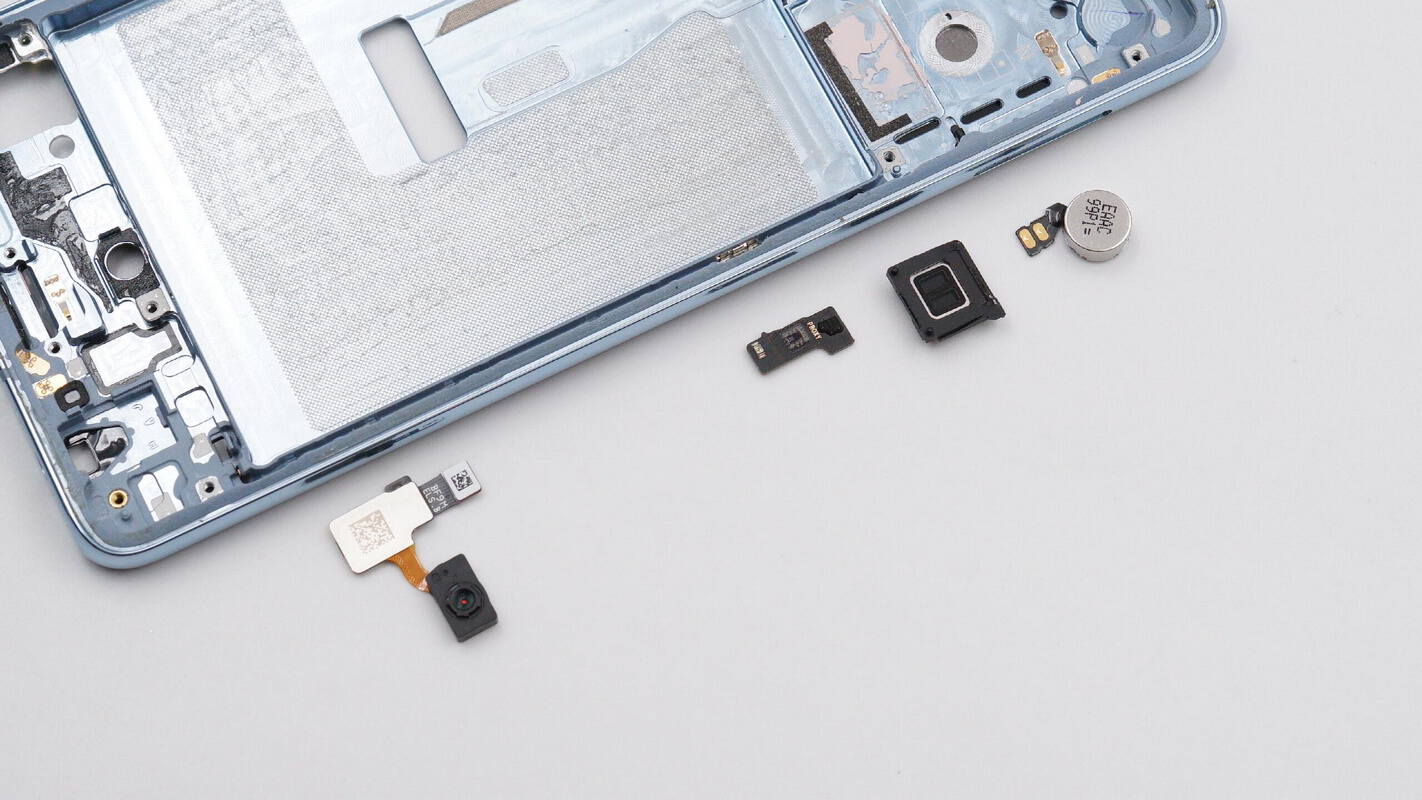
Remove the under-display fingerprint sensor, proximity sensor, earpiece speaker, and vibration motor.
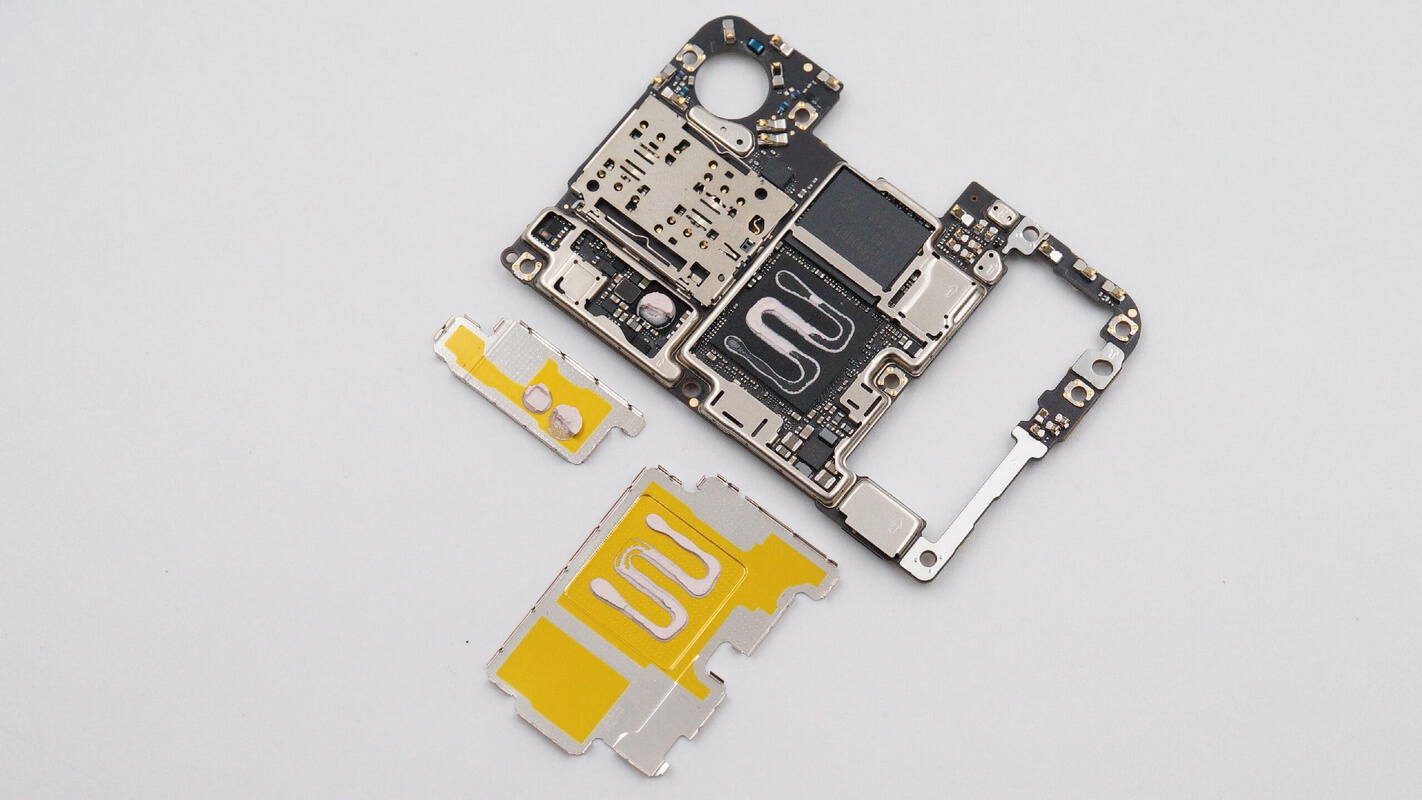
Remove the shielding cover on the front of the main PCB. Thermal gel is applied at the locations corresponding to the processor and power management chips.
Next, remove the shielding cover on the back.
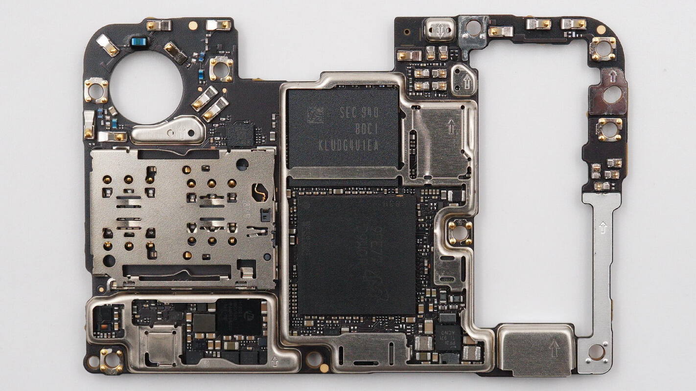
On the front of the main PCB, the SIM card slot is located on the left. Beneath the shielding cover at the bottom is the PMIC. In the center is the UFS storage, with the processor positioned below it. The right side features a cutout area for the camera.
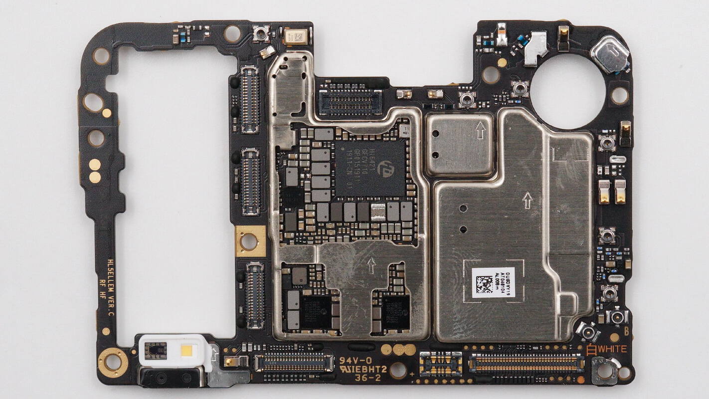
On the back, there is a fill light and a proximity sensor. In the middle are three PMICs, and the shielding cover on the right houses RF-related components.
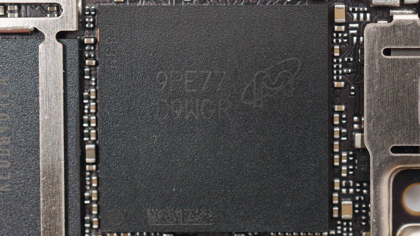
The memory chip is from Micron, marked with D9WGR, model MT53D1G64D8NZ-046 WT: E. It is LPDDR4X memory with a capacity of 8GB, a speed of 4266 Mbps, and uses a 376-ball FBGA package.
Below the memory chip is the Kirin 980 processor, manufactured with TSMC’s 7nm process. It integrates the CPU, GPU, NPU, ISP, and DSP. The CPU configuration is 2× Cortex-A76 at 2.6 GHz, 2× Cortex-A76 at 1.92 GHz, and 4× Cortex-A55 at 1.8 GHz, while the GPU is a Mali-G76 MP10.
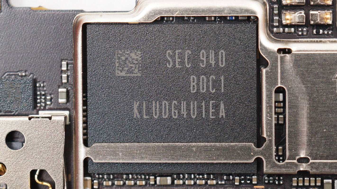
The UFS storage is from Samsung, model KLUDG4U1EA-B0C1. It conforms to the UFS 2.1 standard, has a capacity of 128GB, and uses a G32 lane interface.
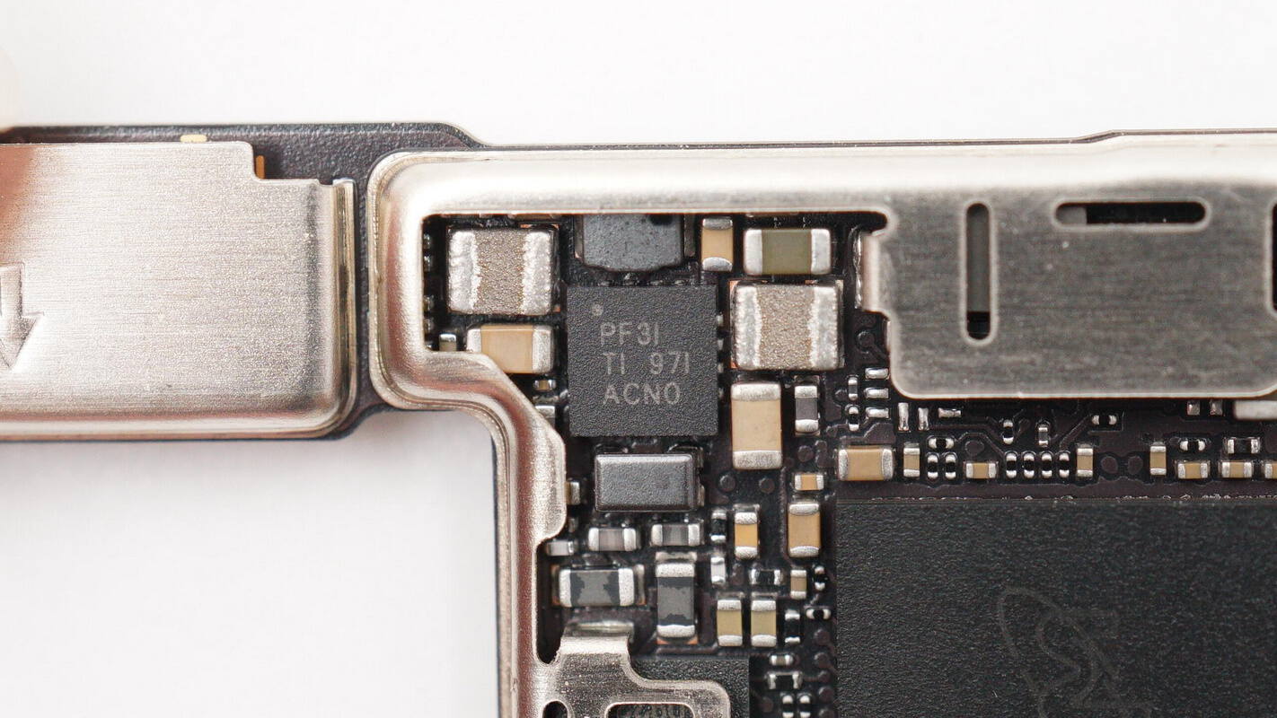
The power conversion chip is from Texas Instruments, marked with PF3I.
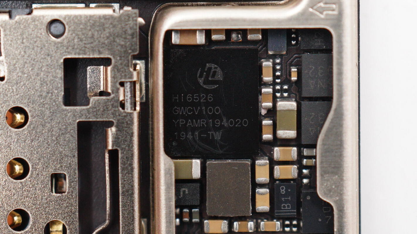
Close-up of the HiSilicon Hi6526 power management IC.
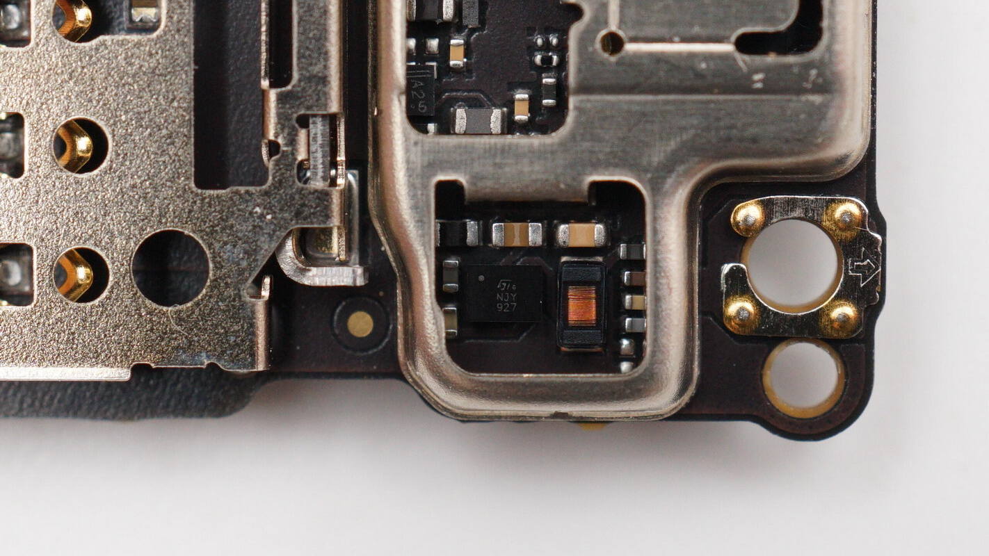
Close-up of the STMicro chip marked with NJY.
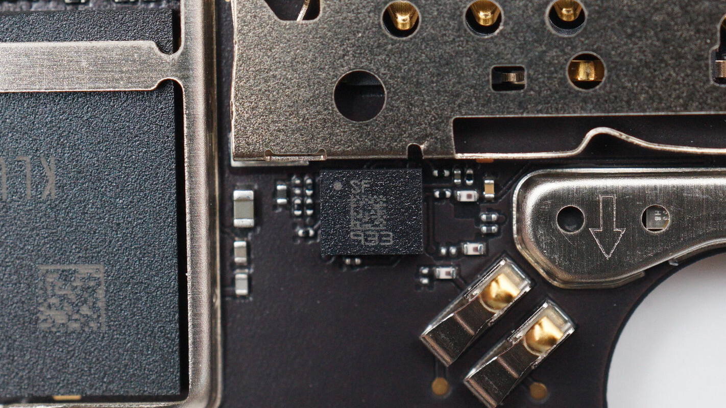
The gyroscope is from STMicro, marked with SF, model LSM6DSL. It integrates a 3D digital accelerometer and a 3D digital gyroscope, and comes in an LGA package.
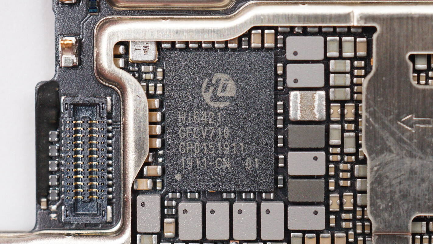
Inside the shielding cover is the HiSilicon Hi6421 power management chip.
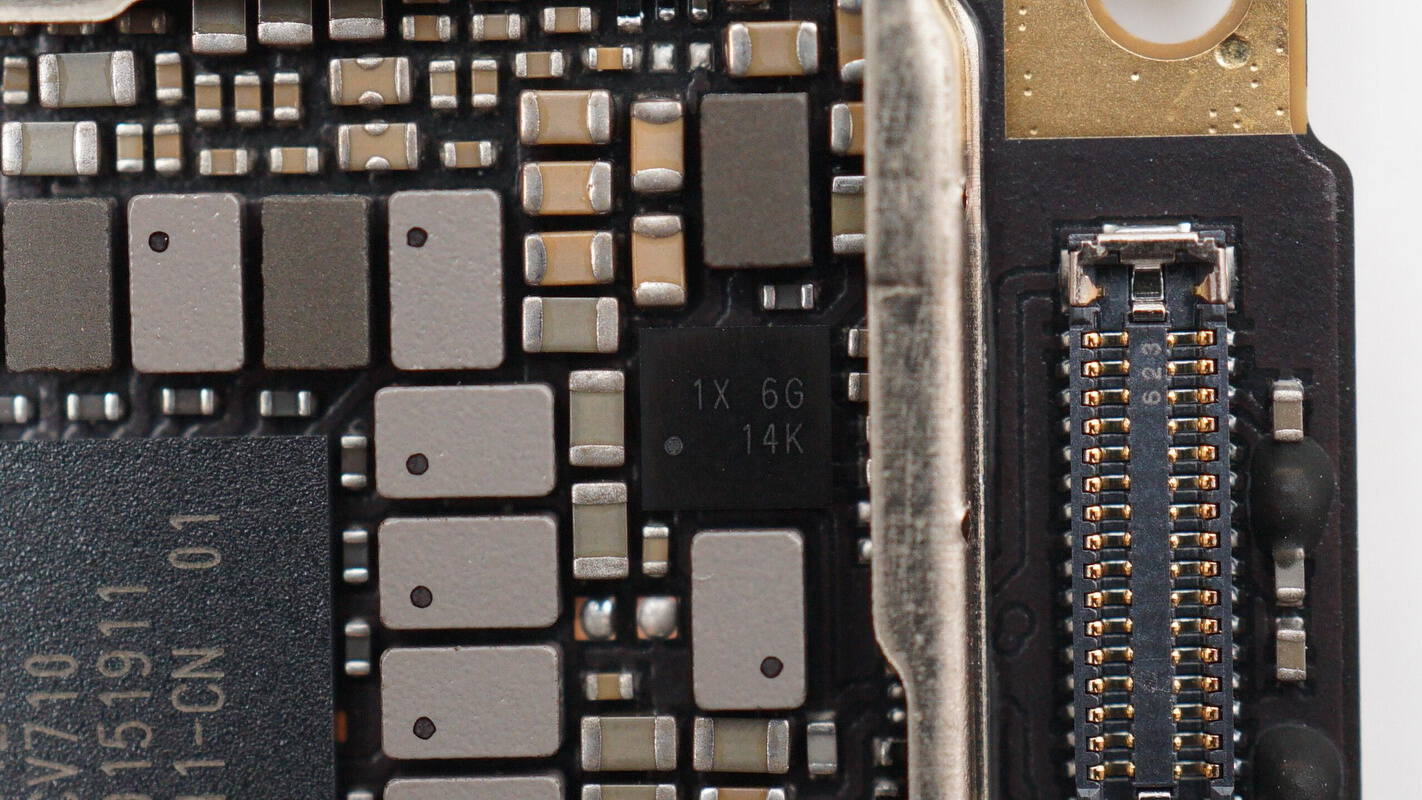
Close-up of the chip marked with 1X 6G 14K.
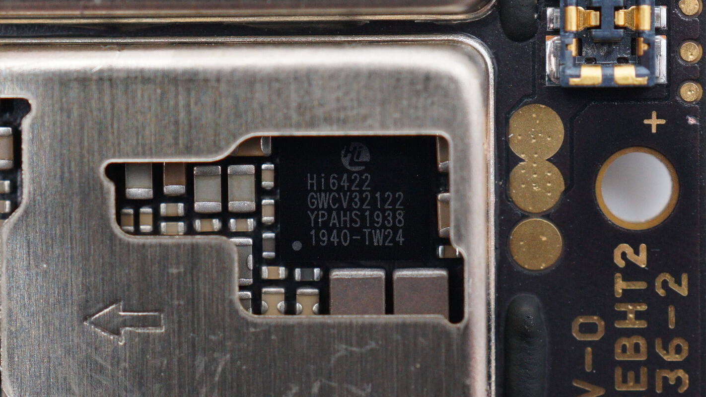
Close-up of the HiSilicon Hi6422 power management chip.
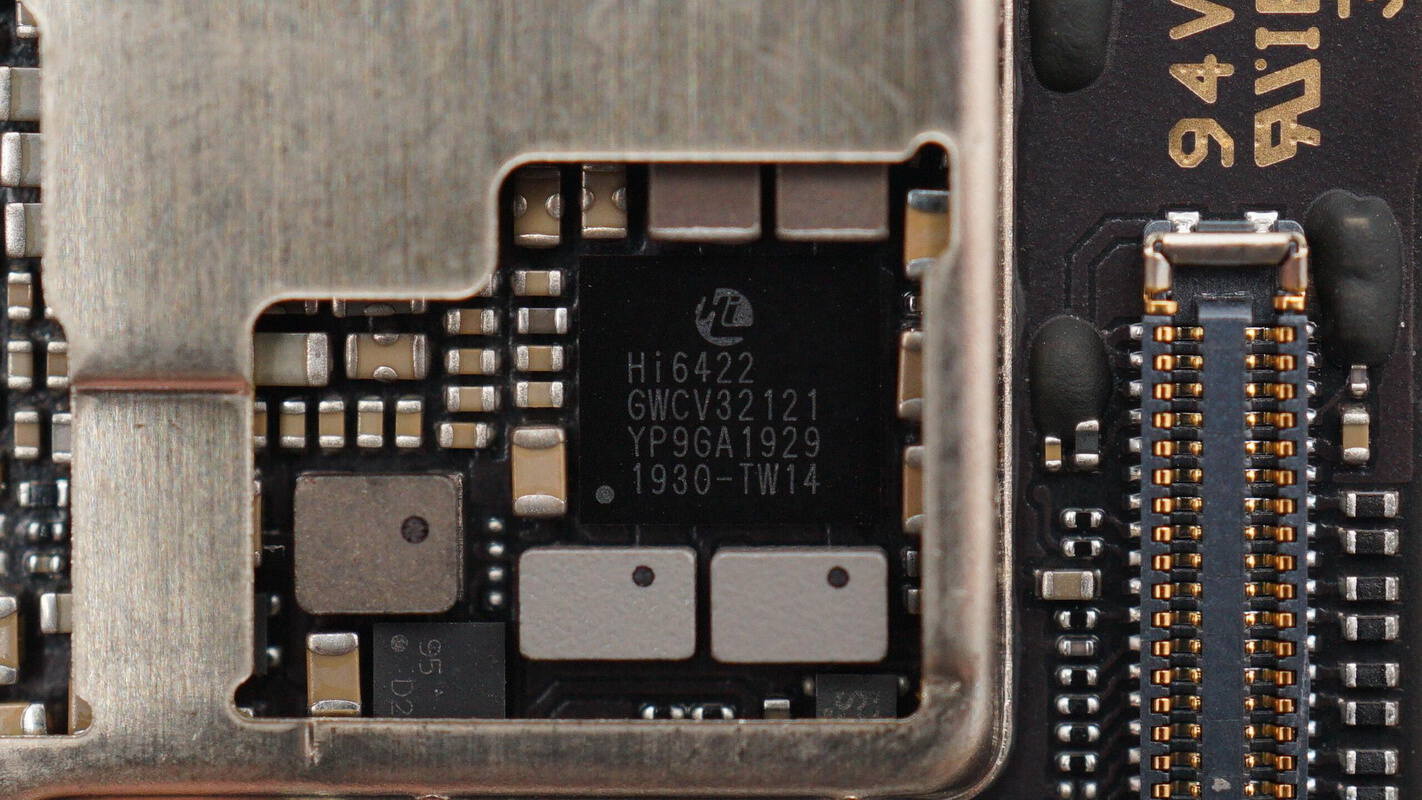
Another power management chip of the same model.
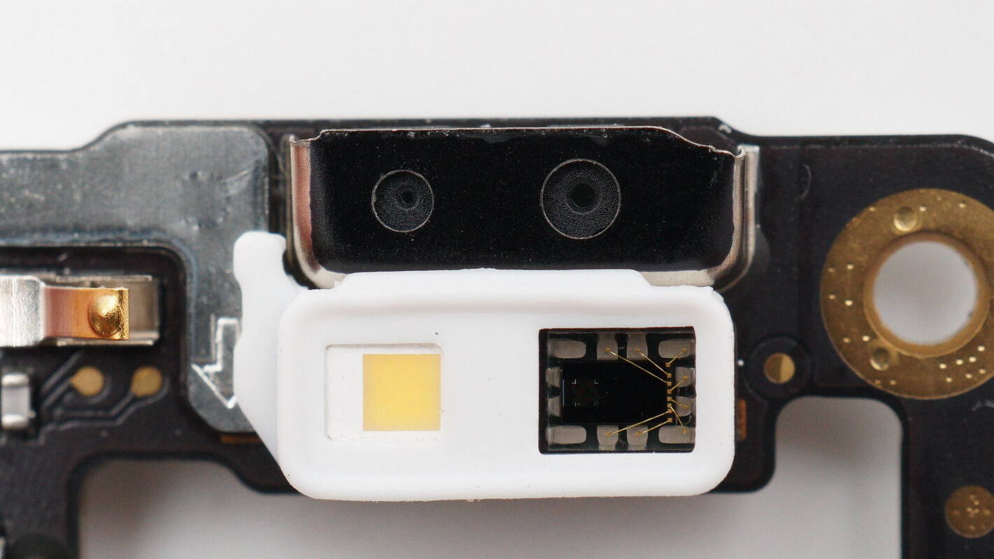
Close-up of the fill light, proximity sensor, and laser sensor.
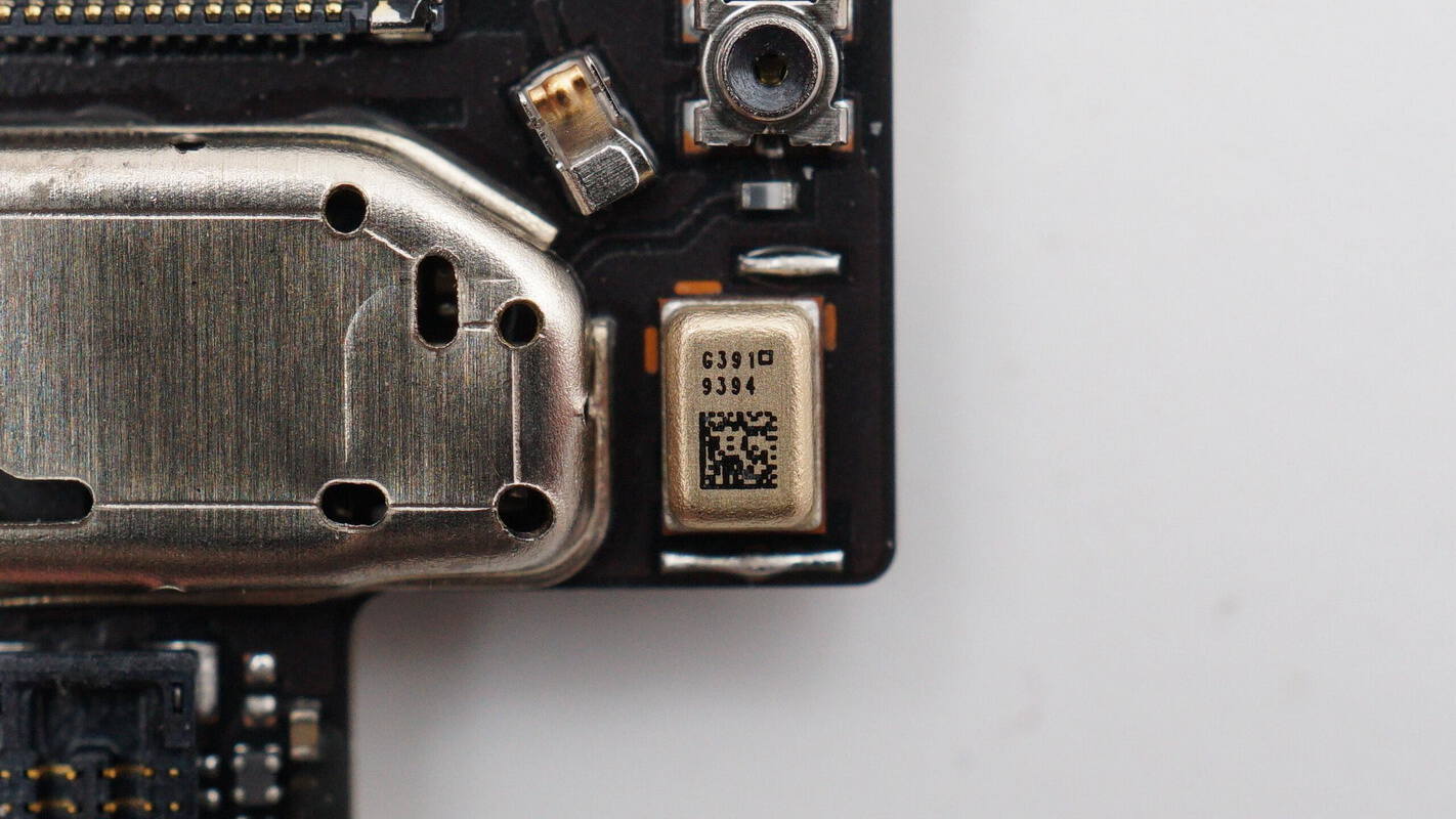
Close-up of the top MEMS microphone.
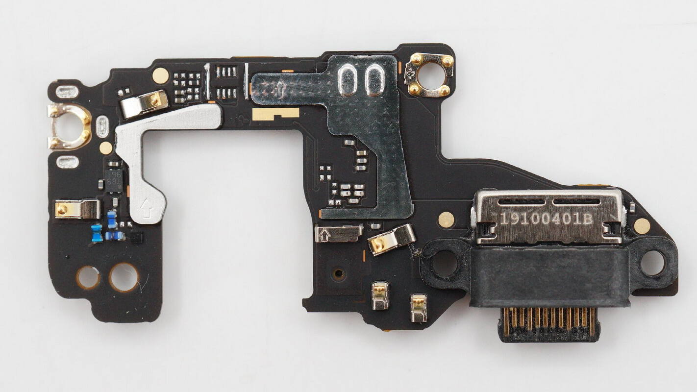
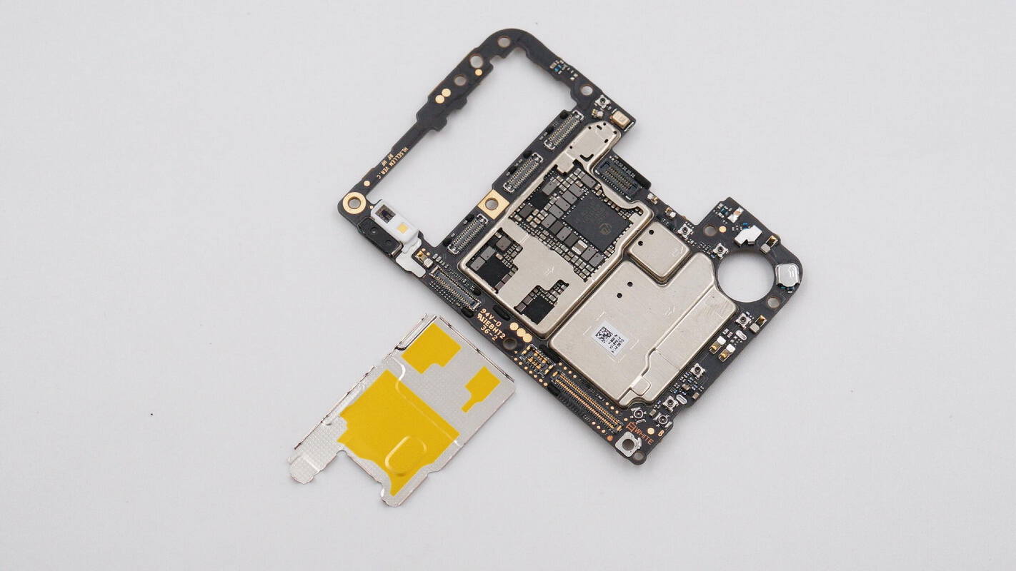
The daughterboard features the USB-C connector.
The other side is equipped with multiple connectors.
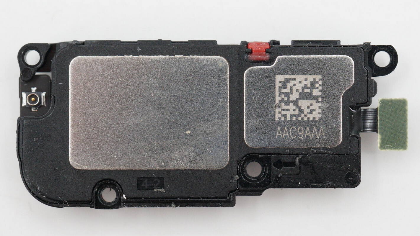
The speaker is laser-engraved with AAC9AAA.
On the back of the speaker assembly, there is a flex cable that connects to the small PCB located at the bottom right.
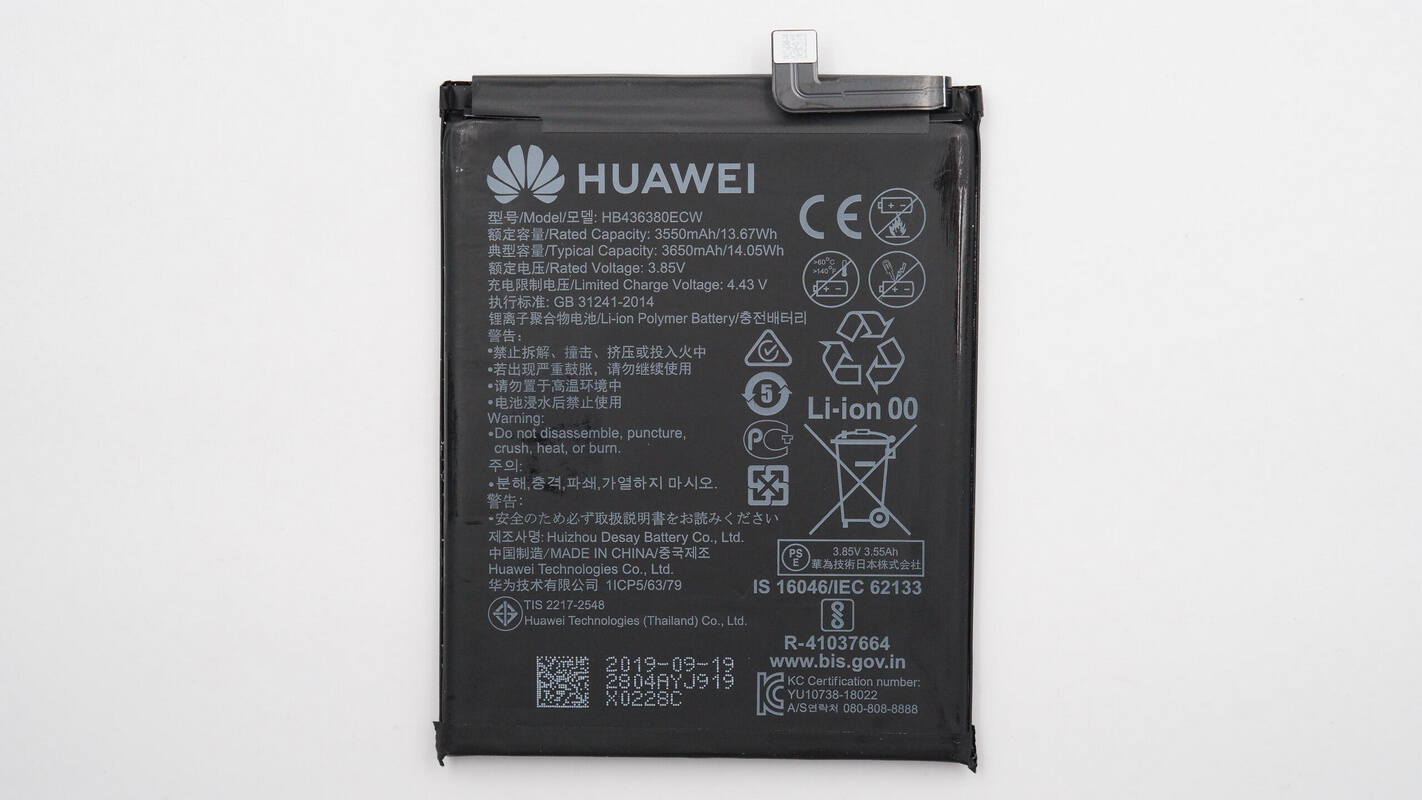
Close-up of the battery specifications:
Rated capacity: 3550 mAh / 13.67 Wh
Typical capacity: 3650 mAh / 14.05 Wh
Rated voltage: 3.85 V
Charge limit voltage: 4.43 V
Standard: GB31241-2014
Type: Lithium-ion polymer battery
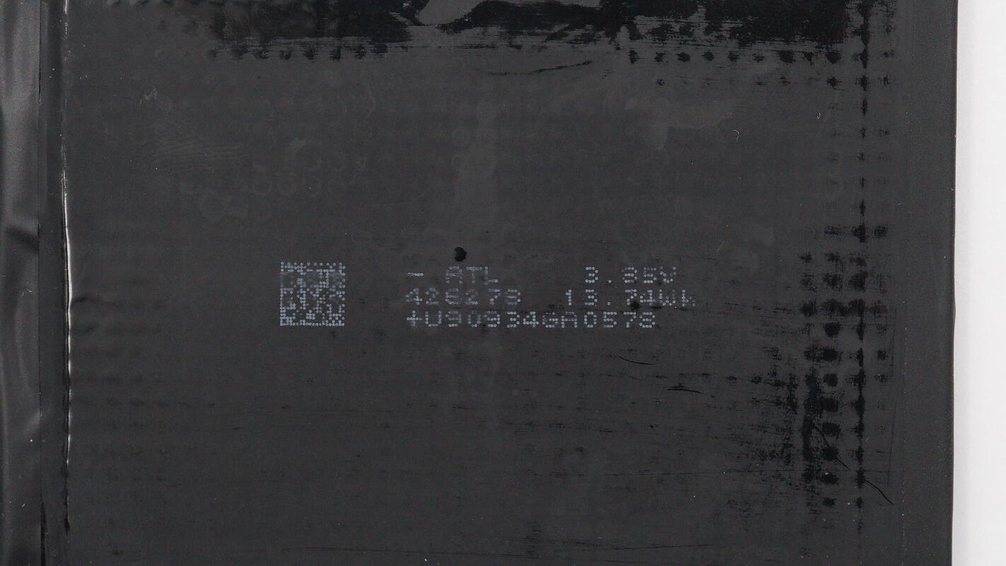
The battery is from ATL, with dimensions of 426278.
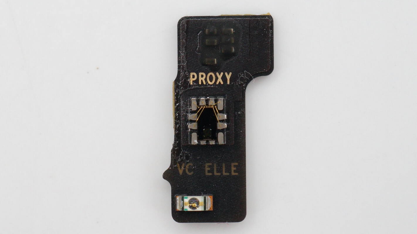
Close-up of the small PCB for the proximity sensor located beneath the display.
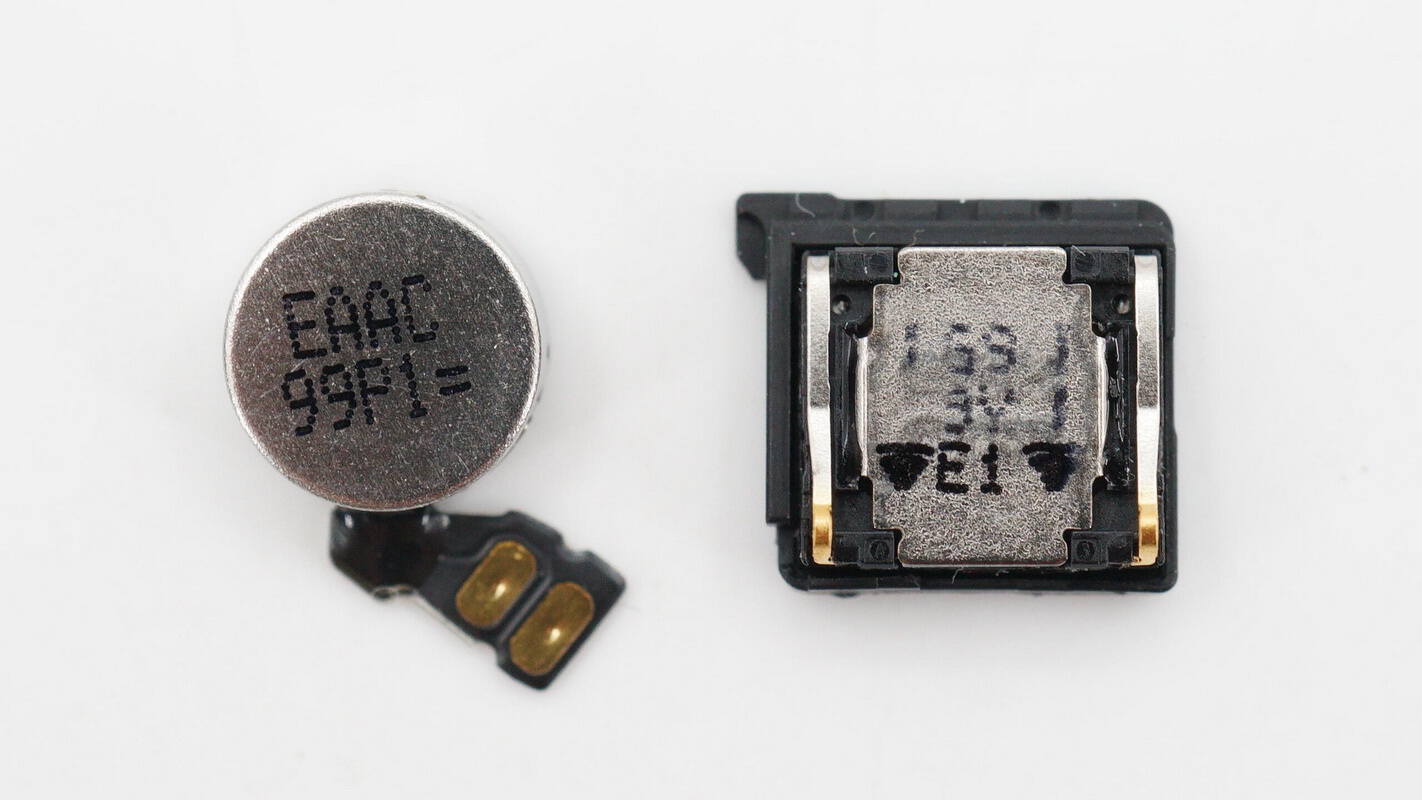
Close-up of the vibration motor and the earpiece speaker.
Close-up of the ultra-thin fingerprint sensor.
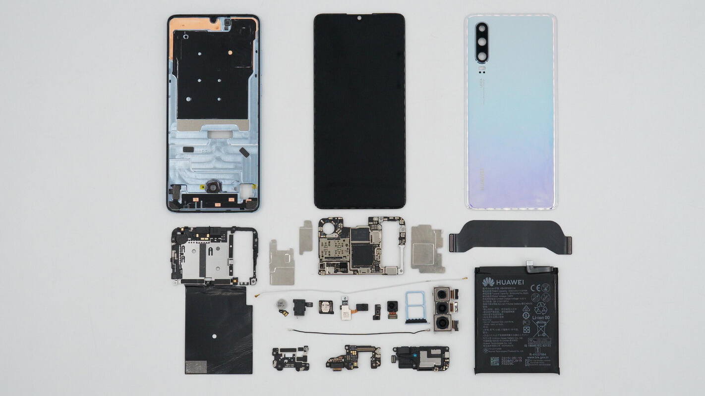
Well, those are all components of the Huawei P30.
Summary of ChargerLAB
The Huawei P30 features a waterdrop display, with the front-facing camera positioned at the top center of the screen and an under-display camera at the bottom for fingerprint recognition. The rear triple-camera setup is vertically aligned, with a fill light and proximity sensor located below. It houses a 3550 mAh battery and supports 22.5 W fast charging.
After taking it apart, we found that it uses a classic three-section design with a compact internal layout. The upper main PCB has a cutout to accommodate the vertically aligned rear cameras and features shielding covers on both the front and back. The main PCB and daughterboard are connected via a flex cable. The battery includes a quick-release pull tab, and the fingerprint sensor is located beneath the battery.
It is powered by the Kirin 980 octa-core processor, paired with 8GB of Micron LPDDR4X memory and 128GB of Samsung UFS storage. Multiple HiSilicon power management chips are used for battery charging and chip power supply. The internal structure is compact, and the cutout design maximizes space utilization.
Related Articles:
1. Teardown of OPPO 50W AirVOOC Magnetic Wireless Charger (OAWV09)
2. Teardown of VMAX AC Power Supply (VT450AB220A)
3. Teardown of OPPO 120W SuperVOOC GaN Charger (OSABBCBBAC)