Introduction
Previously, we disassembled the original Huawei Pura X 66W GaN charger. This time, we've got our hands on the 100W GaN charger from the same series. It combines a compact size with powerful performance, supporting Huawei's 66W SuperCharge, 100W UFCS, and 65W PD. It's more than capable of charging Huawei Mate 70 series, Pura X models, and even laptops with ease. Next, let's take it apart to see its internal components and structure.
Product Appearance
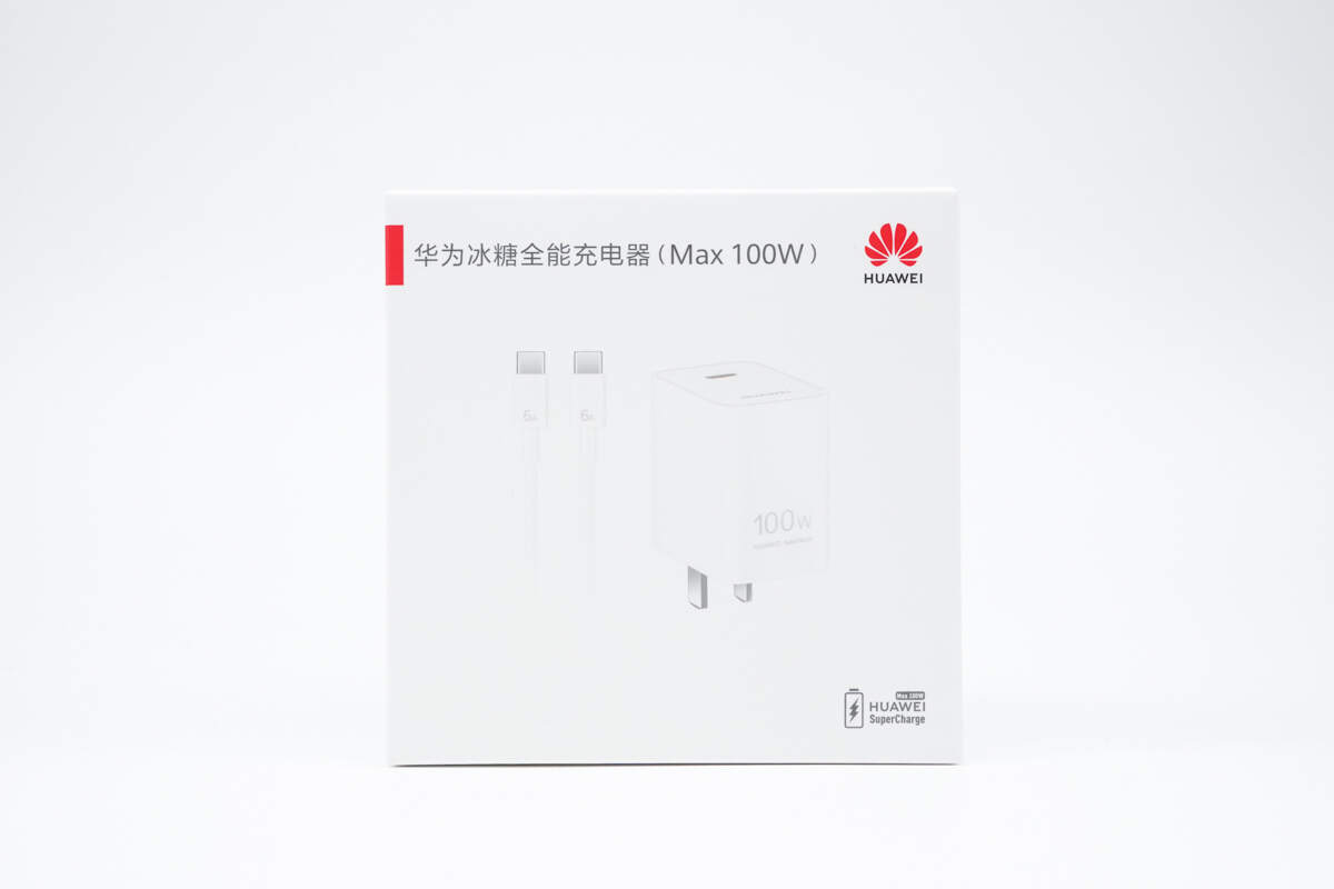
The packaging is printed with the Huawei logo, name, product appearance, and HUAWEI SuperCharge logo.
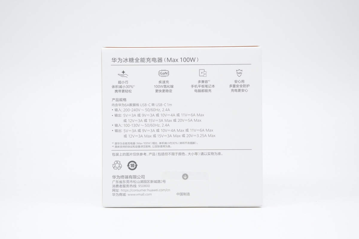
The specs info and selling points are printed on the back.
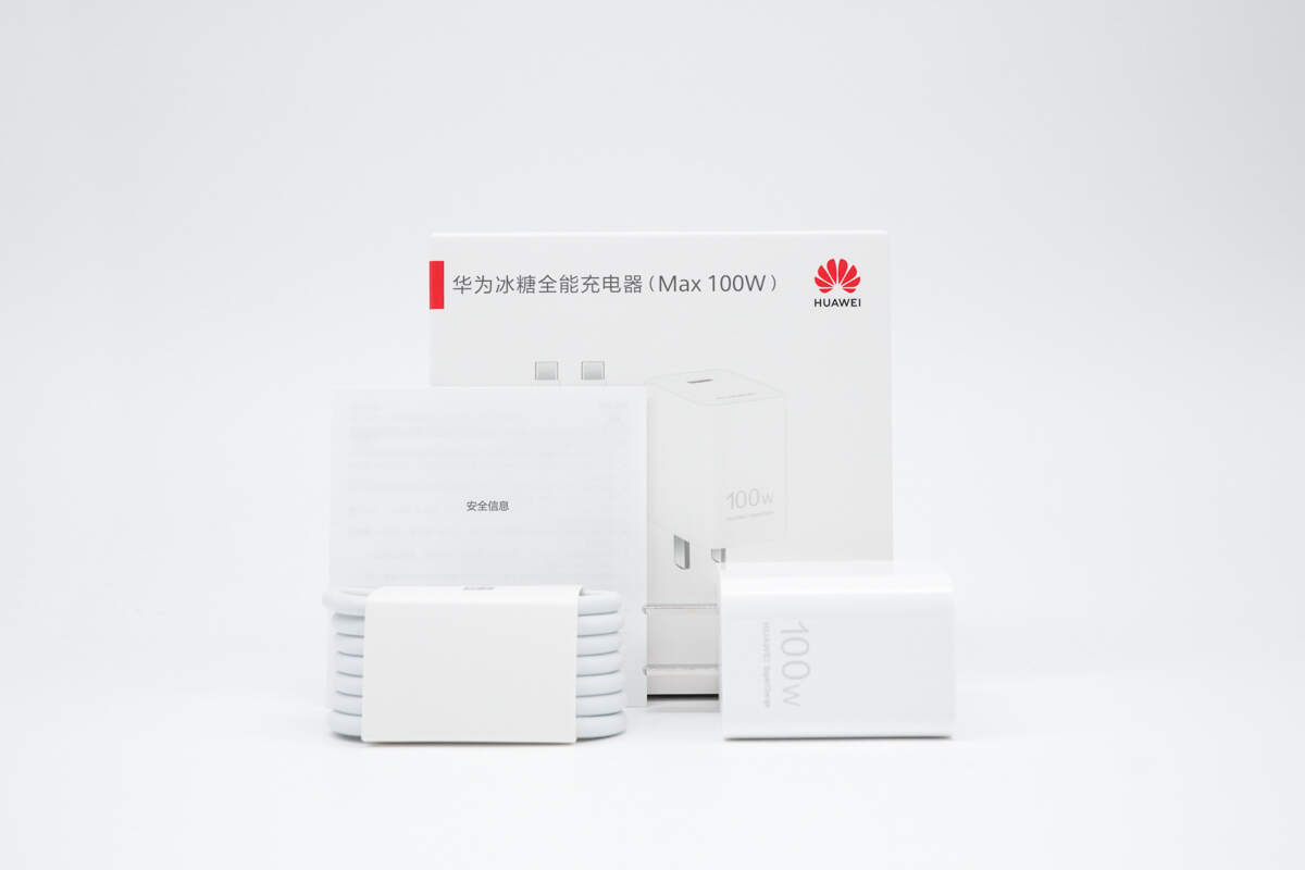
The packaging contains the charger, cable, and some documents.
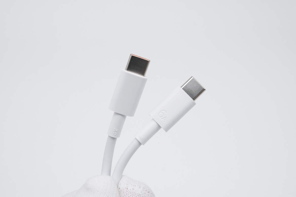
The dual USB-C cable is engraved with 6A.
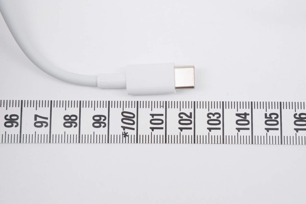
The length of the cable is about 1 m (3' 3.37'').
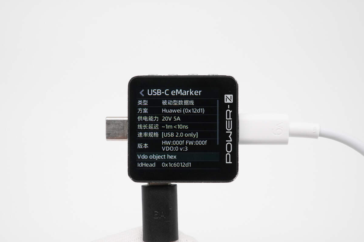
ChargerLAB POWER-Z KM003C shows it has an E-marker chip, supports 20V5A, and USB 2.0.
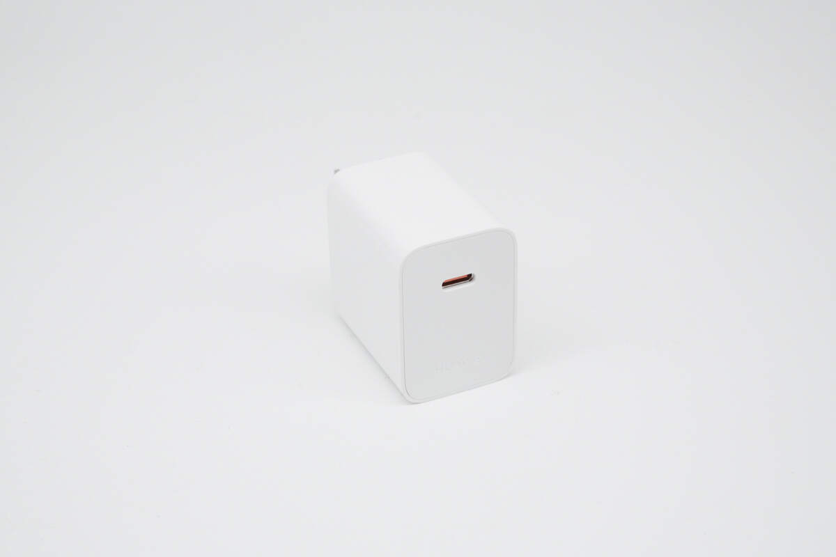
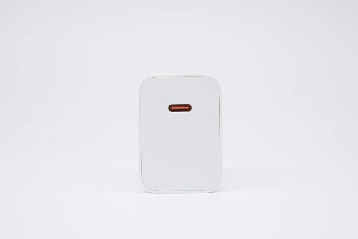
The charger has a minimalist design. Compared to the 66W version, it is shorter but wider.
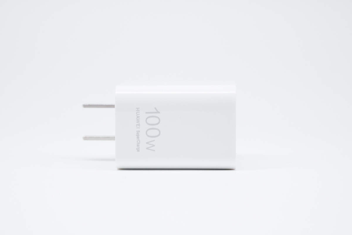
100W and HUAWEI SuperCharge are printed on the front.
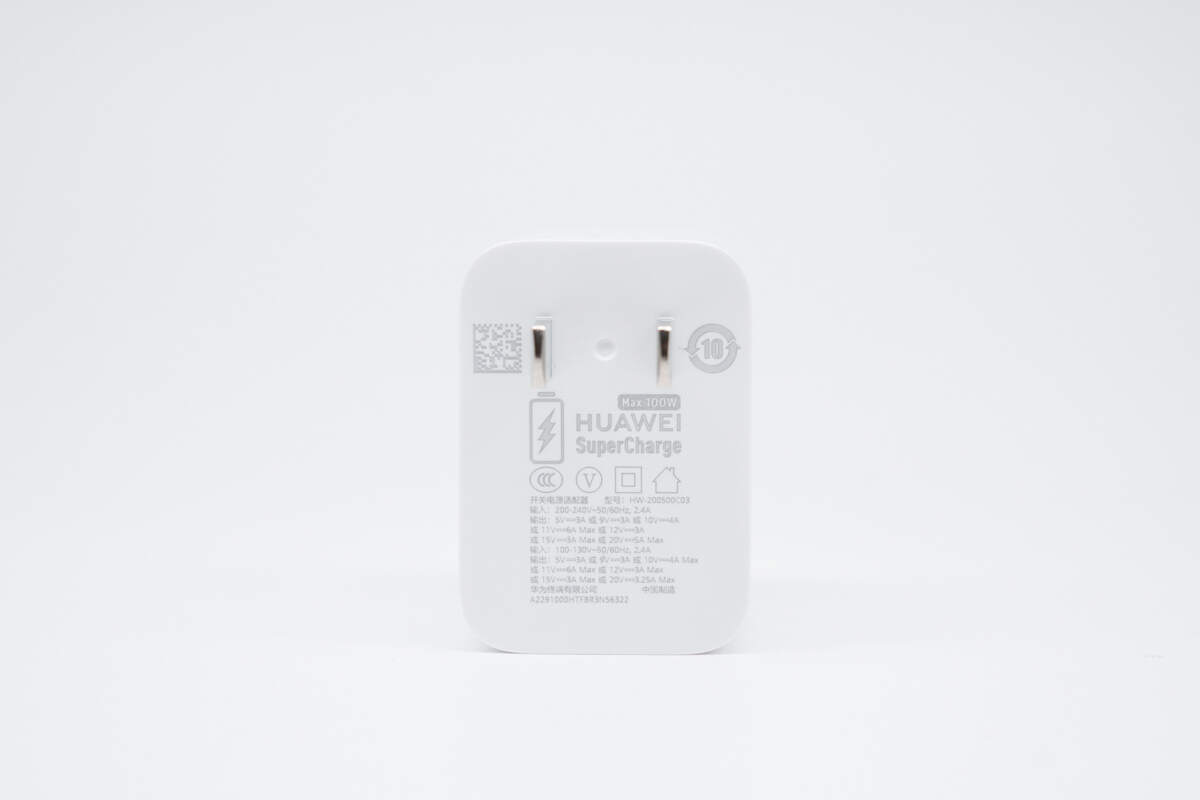
The spec info is printed on the input end.
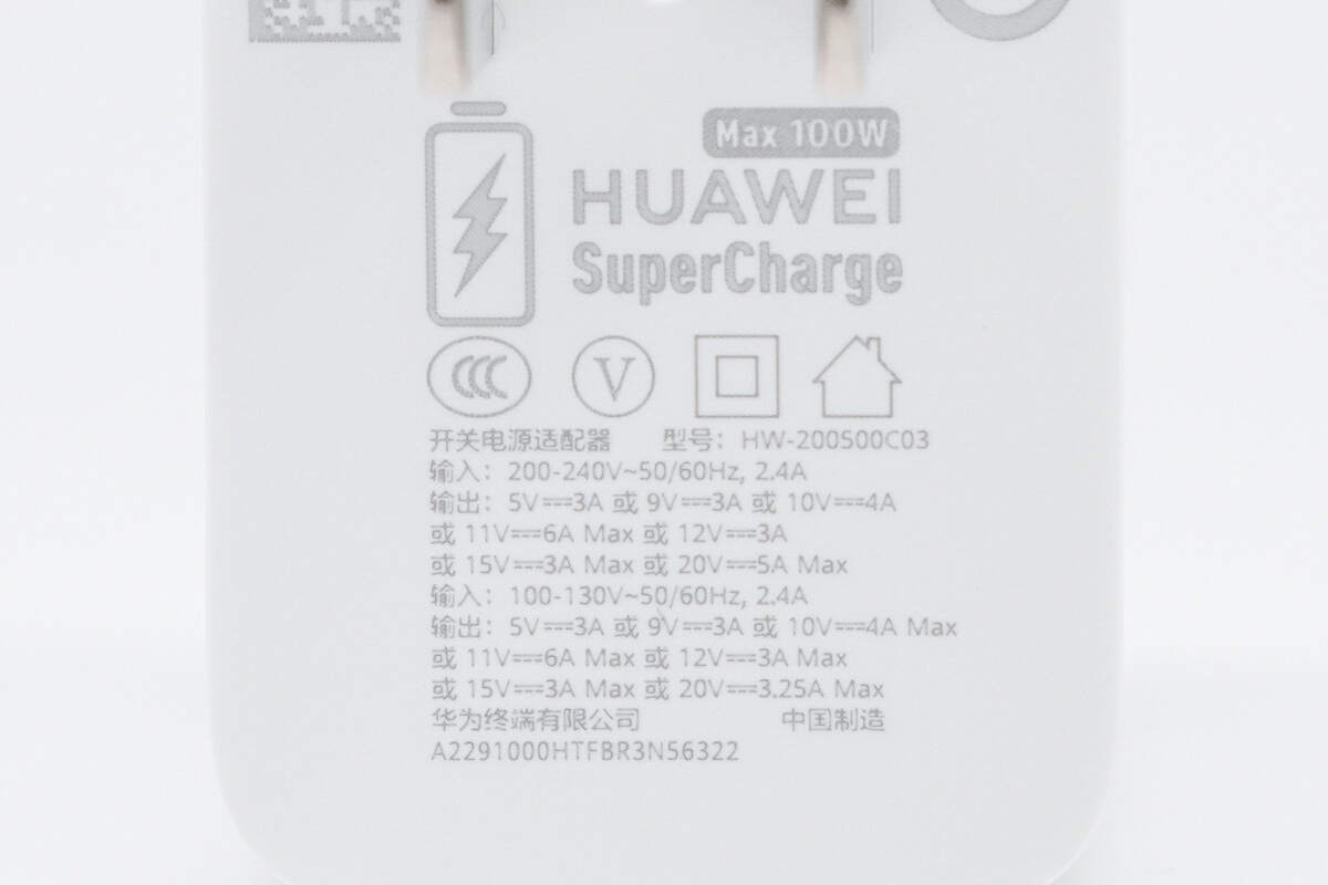
Model: HW-200500C03
Input: 200-240V~50/60Hz 2.4A
Output: 5V3A, 9V3A, 10V4A, 11V6A, 12V3A, 15V3A, 20V5A Max
Input: 100-130V~50/60Hz 2.4A
Output: 5V3A, 9V3A, 10V4A, 11V6A, 12V3A, 15V3A, 20V3.25A Max
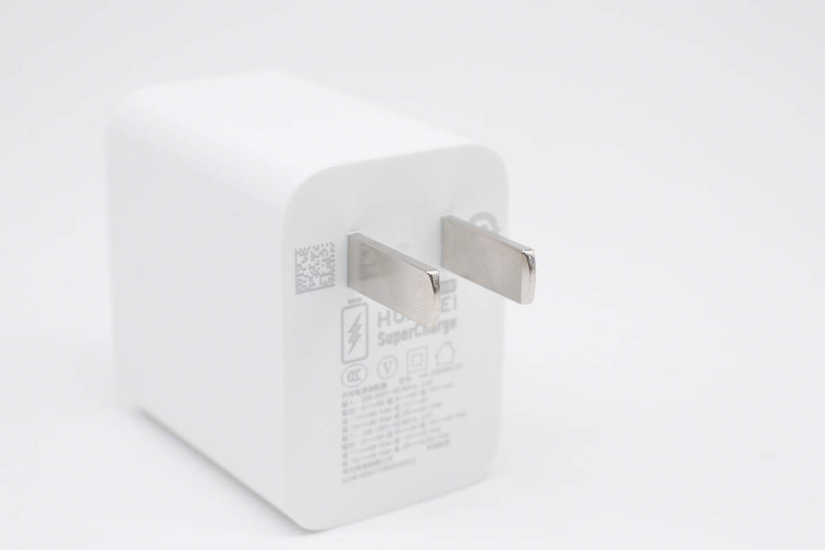
It adopts a fixed plug.
The plastic sheet is orange.
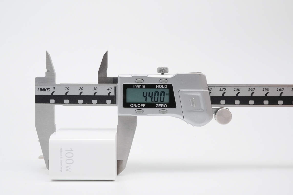
The length of the charger is about 44 mm (1.73 inches).
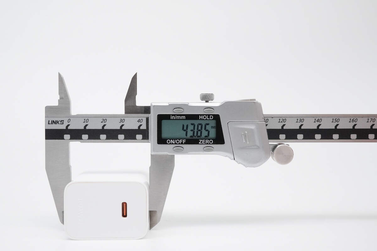
The width is about 43.85 mm (1.73 inches).
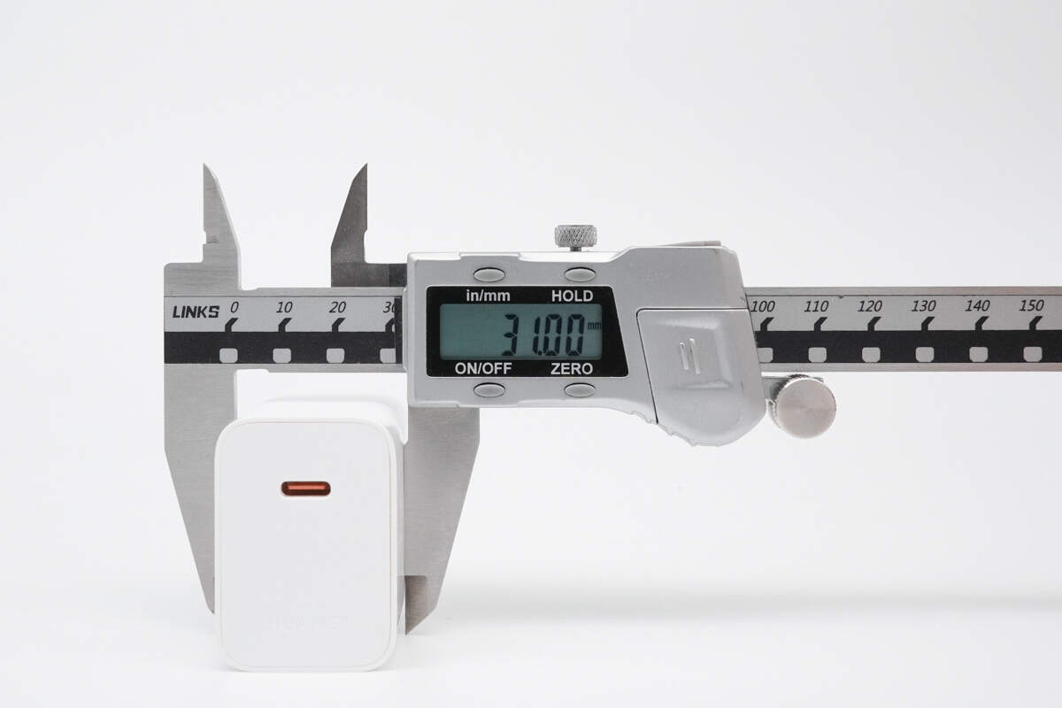
The thickness is about 31 mm (1.22 inches).
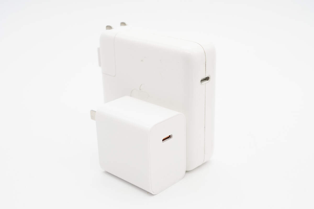
It is much smaller than the Apple 96W charger.
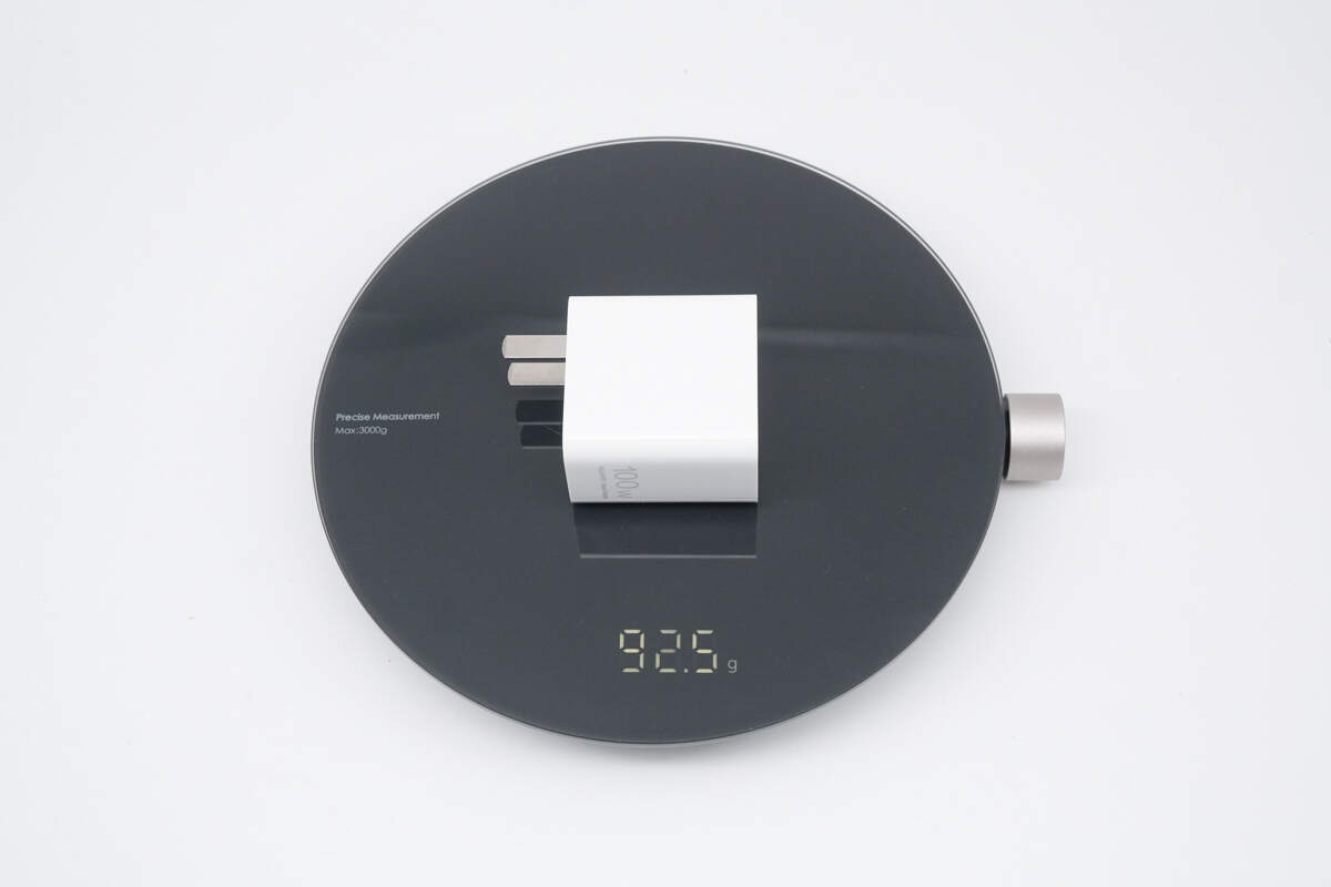
The weight is about 93 g (3.28 oz).
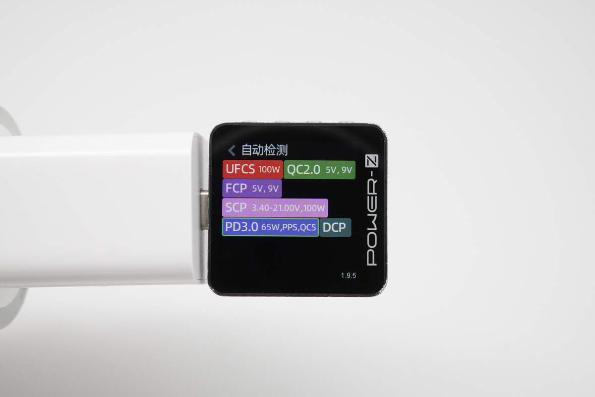
ChargerLAB POWER-Z KM003C shows the USB-C port can support UFCS, FCP, SCP, QC2.0/5, PD3.0, PPS, and DCP charging protocols.
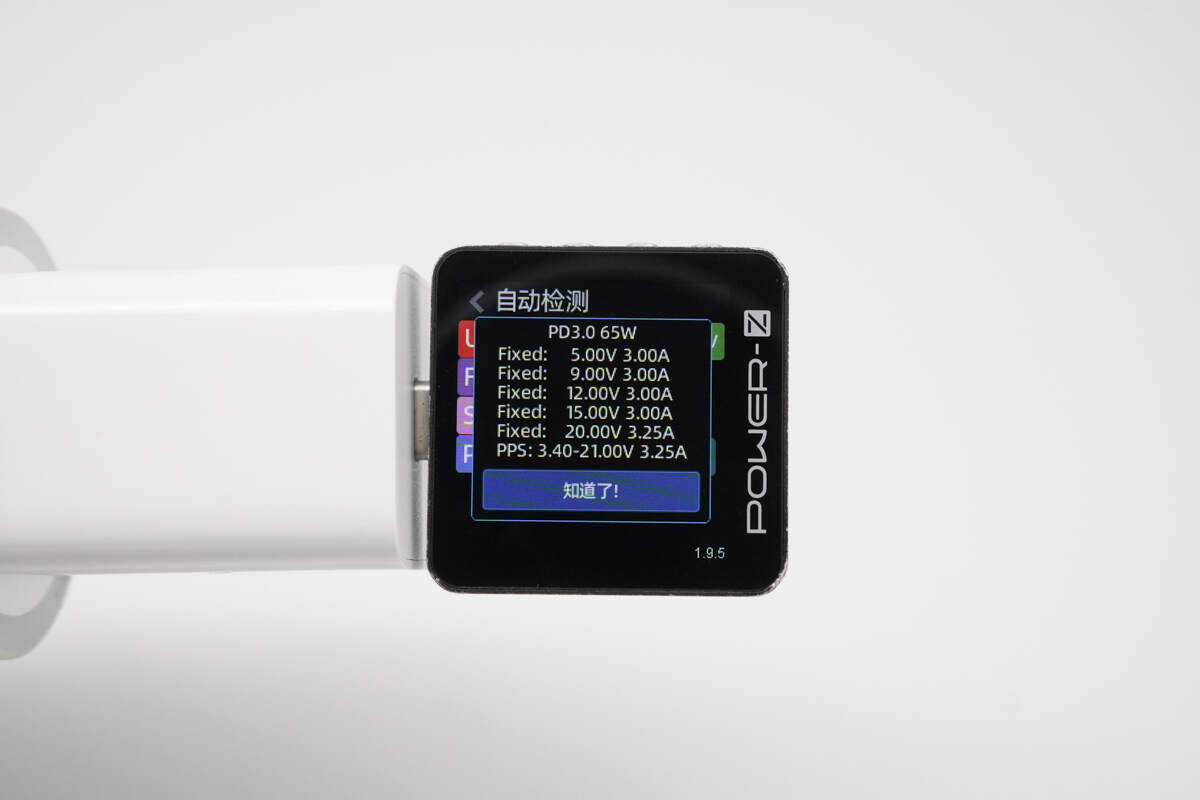
And it has five fixed PDOs of 5V3A, 9V3A, 12V3A, 15V3A, and 20V3.25A. It also has a set of PPS, which is 3.4-21V 3.25A.
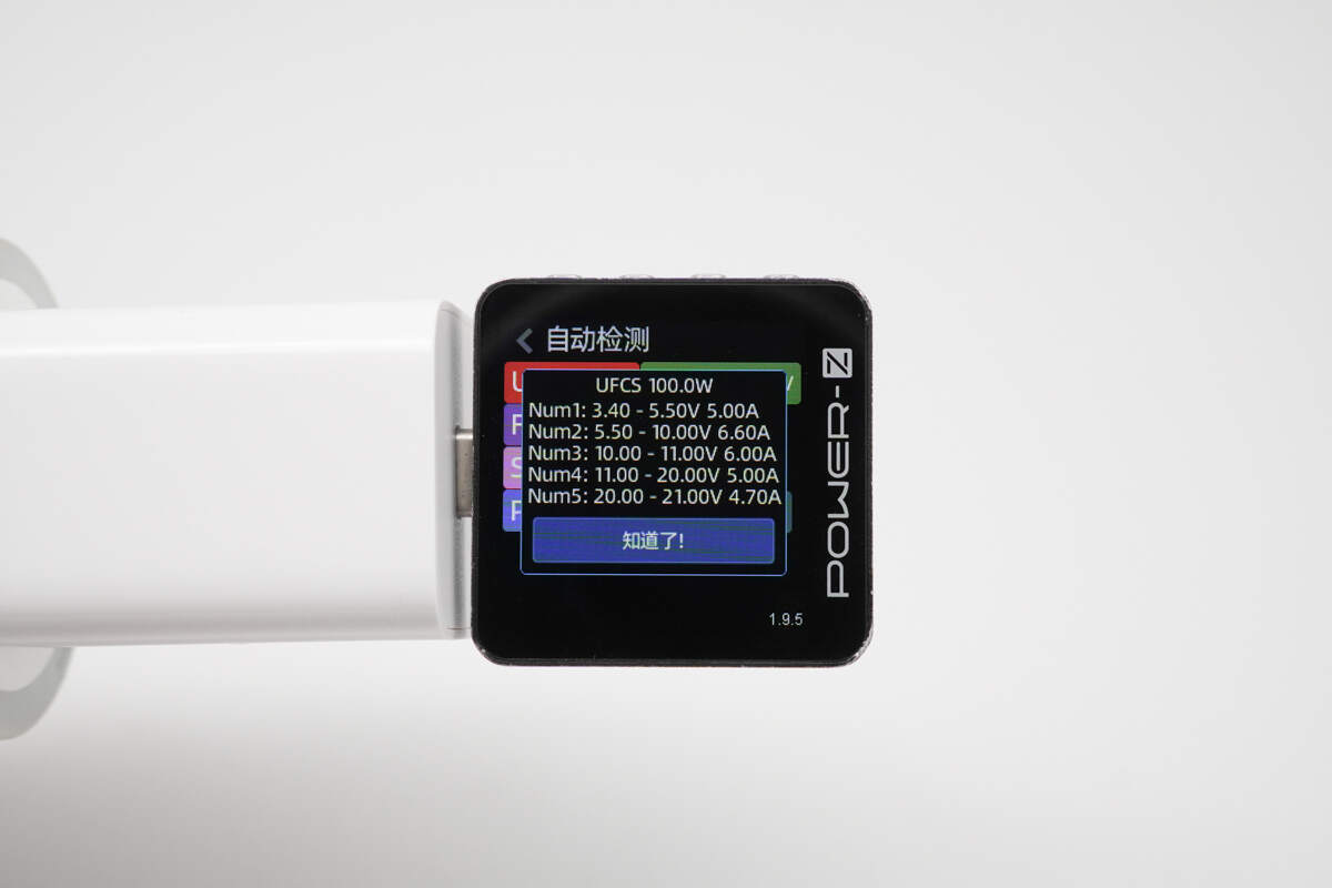
It has five sets of UFCS, which are 3.4-5.5V 5A, 5.5-10V 6.6A, 10-11V 6A, 11-20V 5A, and 20-21V 4.7A.
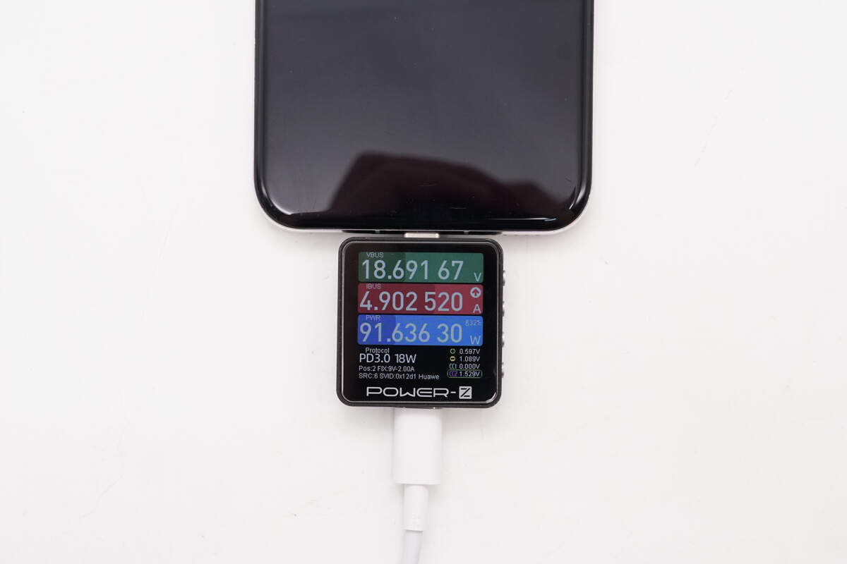
Use it to charge Huawei Pura X, the charging power is about 91.64W.
Teardown
Next, let's take it apart to see its internal components and structure.
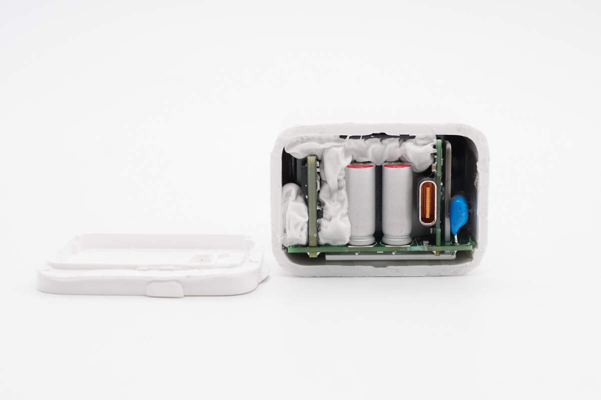
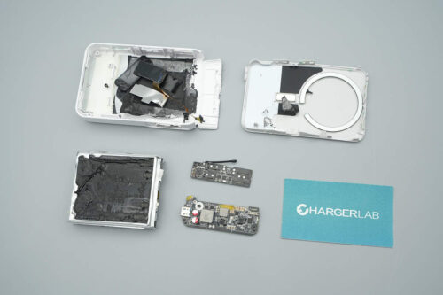
Disassemble the output end cover.
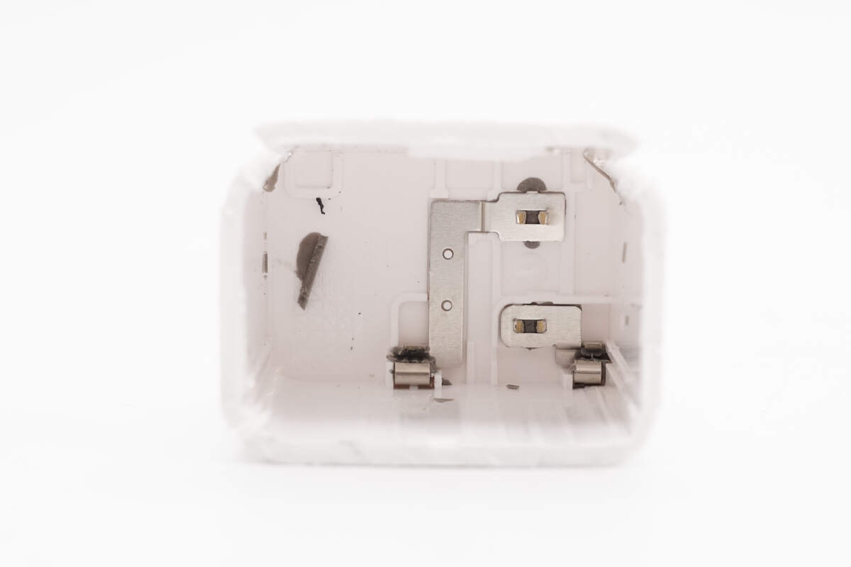
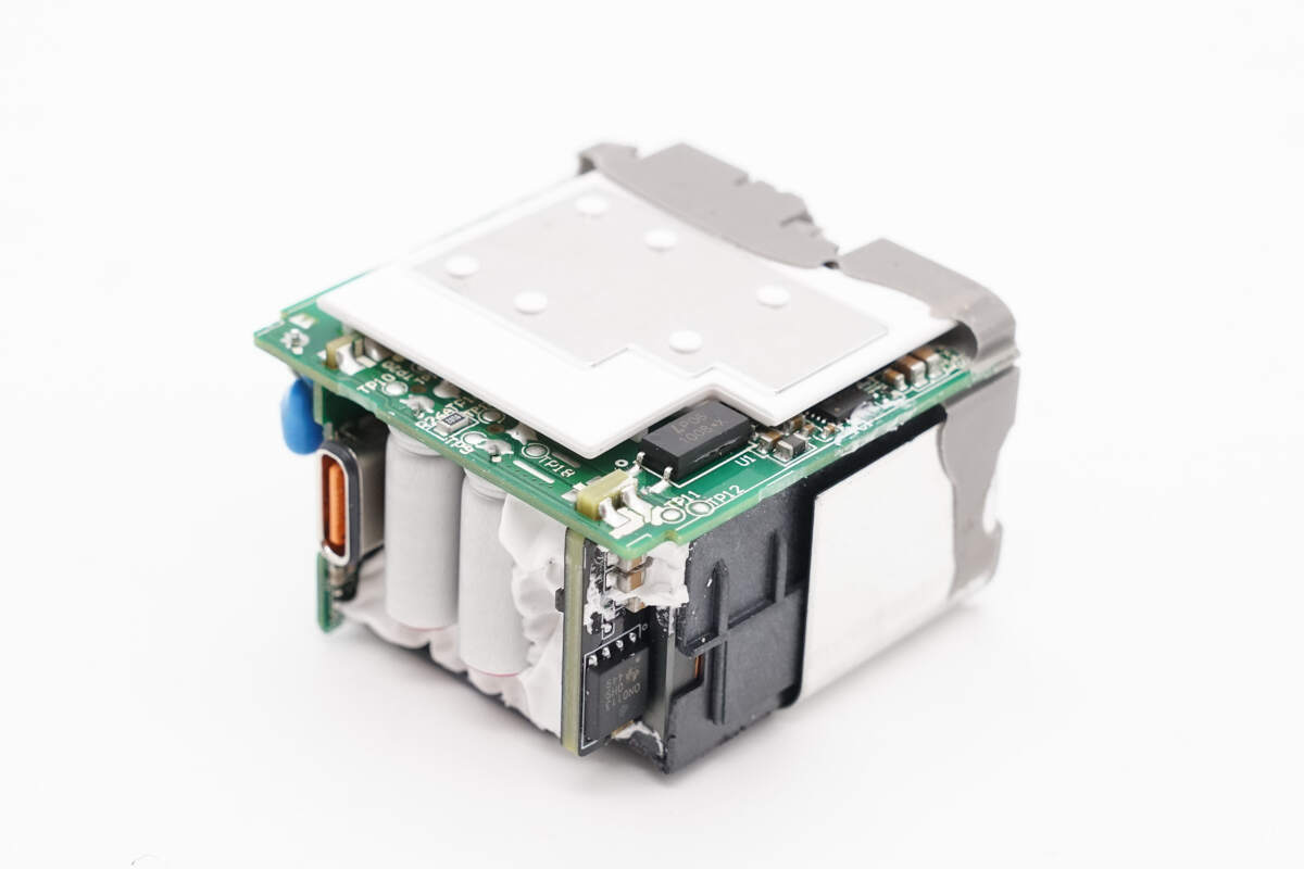
Take out the PCBA module. The input pins are press-fitted with metal shrapnel, using a contact-based power delivery design.
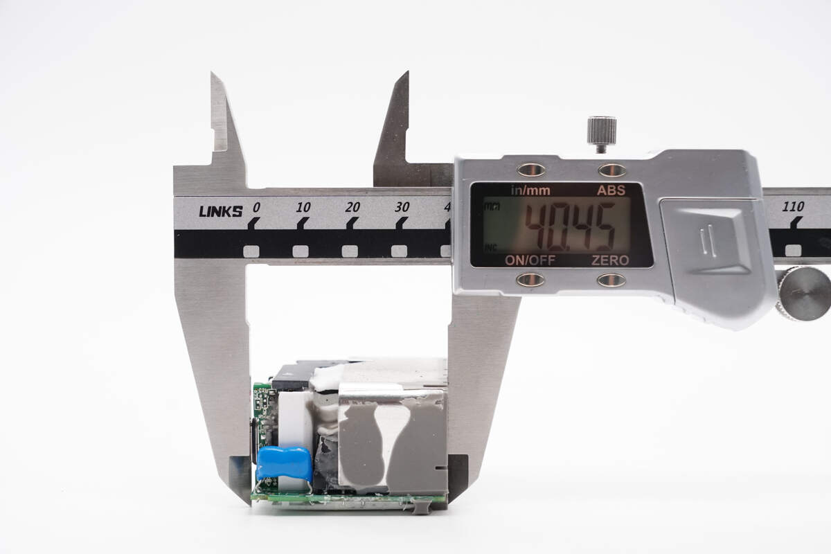
The length of the PCBA module is about 40.45 mm (1.59 inches).
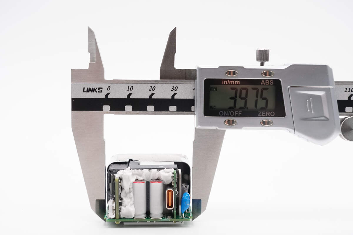
The width is about 39.75 mm (1.56 inches).
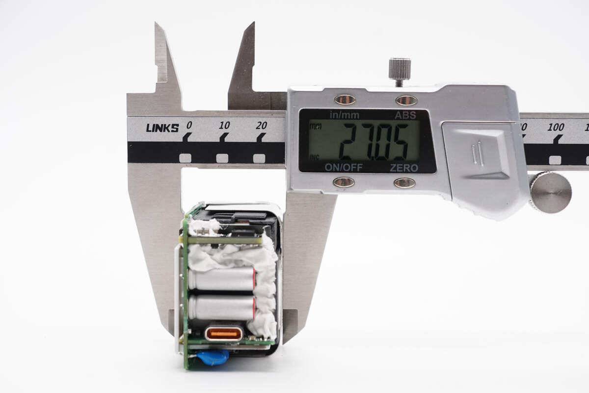
The thickness is about 27.05 mm (1.065 inches).
The input end of the PCBA module is designed for a contact power supply.
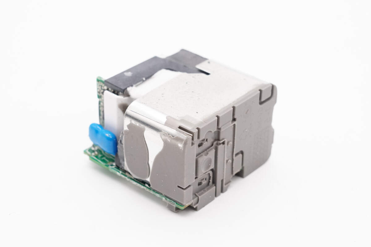
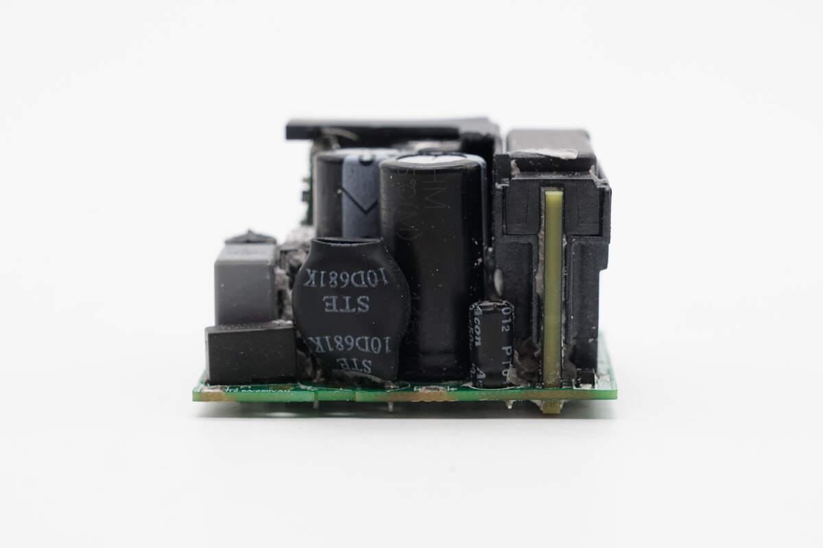
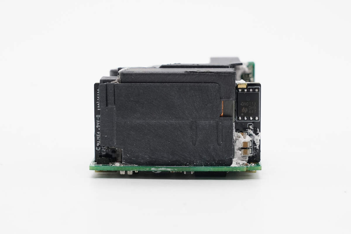
The module is covered with heat sinks, with a plastic isolation plate between the primary and secondary sides. The gaps between components are filled with potting compound for reinforcement.
The back of the module is covered with an insulating plate and a heat sink.
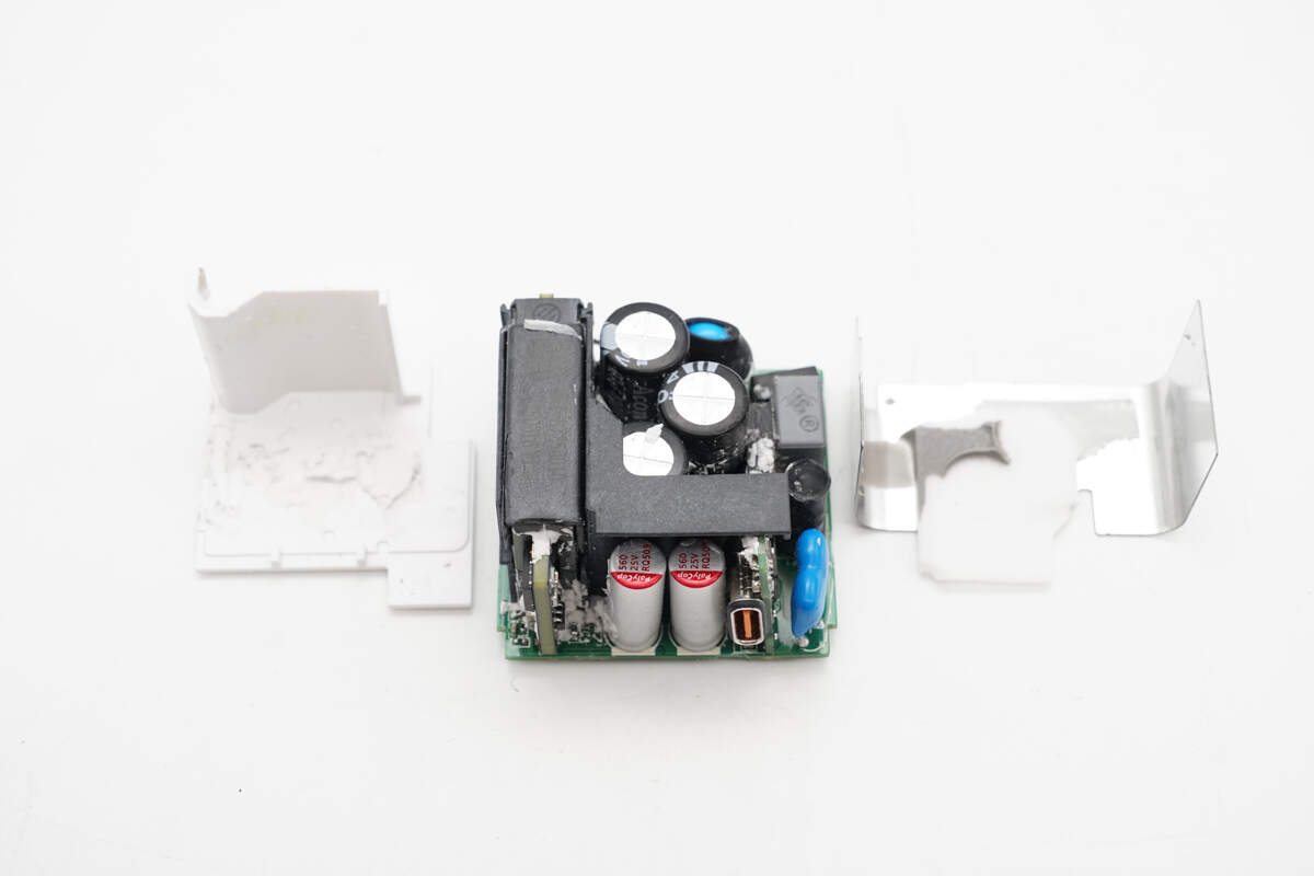
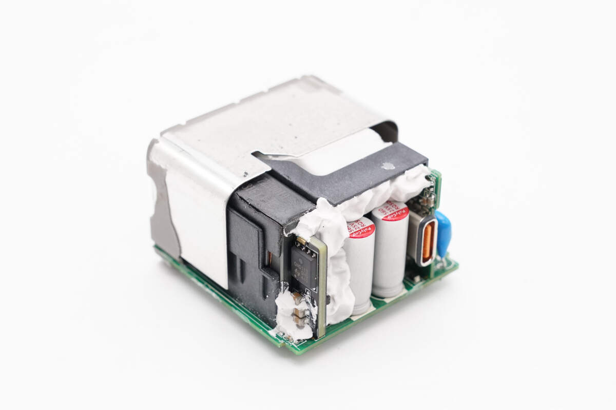
Remove the heat sinks and clean off the potting compound.
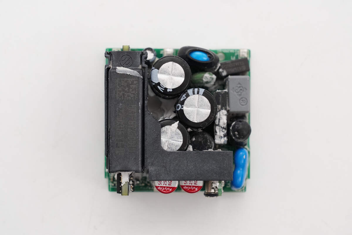
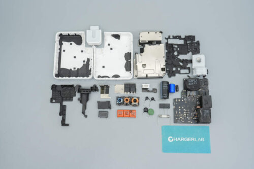
The module includes components such as a time-delay fuse, a safety X2 capacitor, and capacitors. On the left side, there is also a planar transformer module, with a compact component layout.
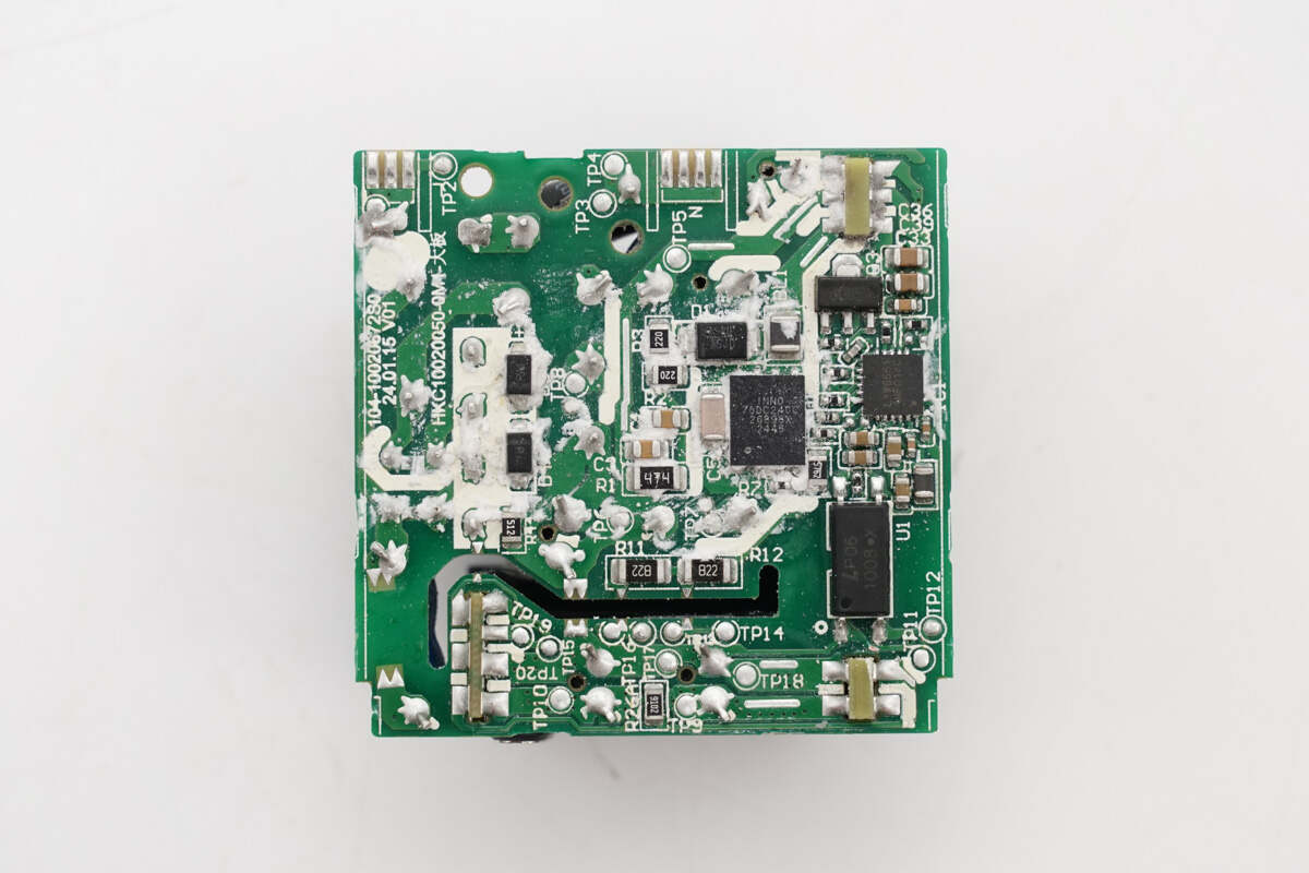
On the back, there are components such as the master control chip, MOSFET, and optocoupler.
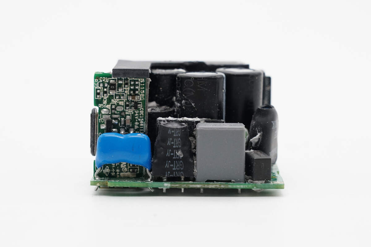
On this side, there are components such as the time-delay fuse, safety X2 capacitor, common mode choke, bridge rectifier, and I-shaped inductor.
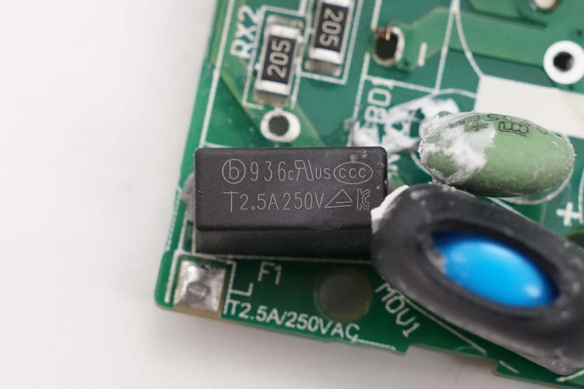
The time-delay fuse is from Betterfuse. 2.5A 250V.
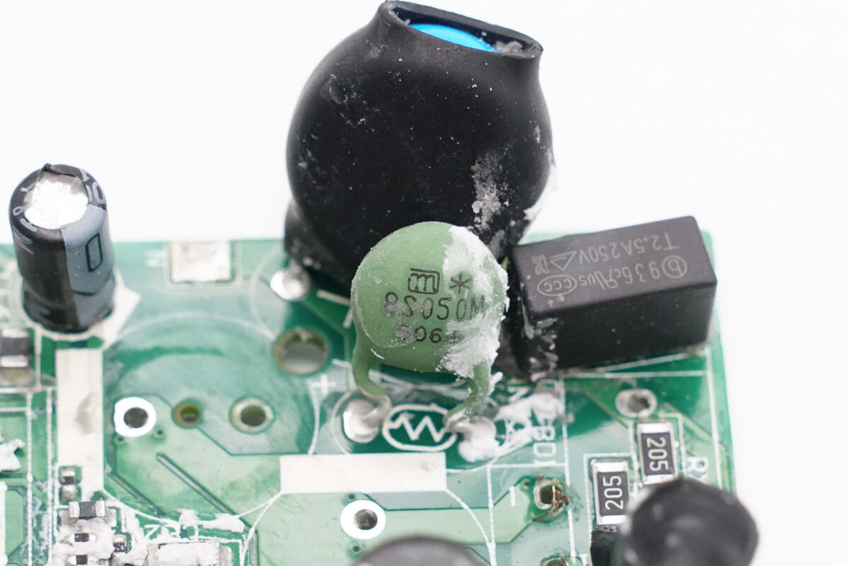
The NTC thermistor is used to suppress inrush current during power-up.
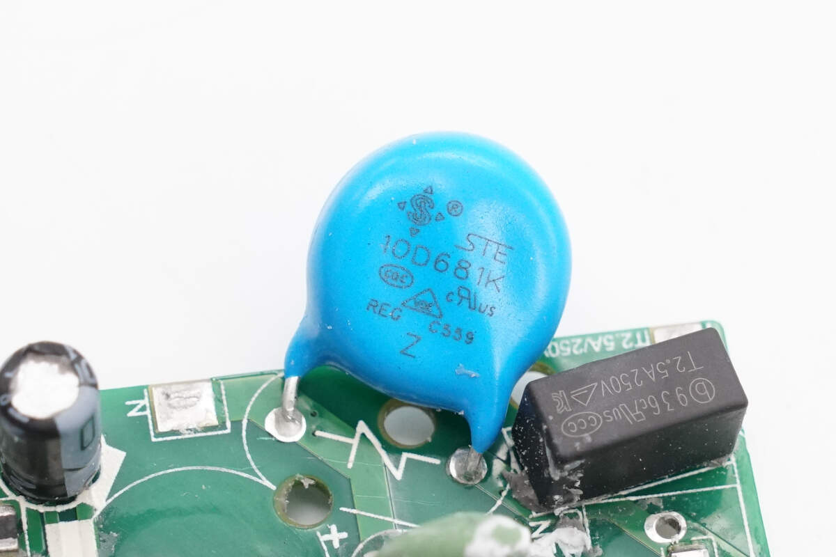
The varistor is from STE, with the specification 10D681K, and is insulated by heat-shrinkable tubing.
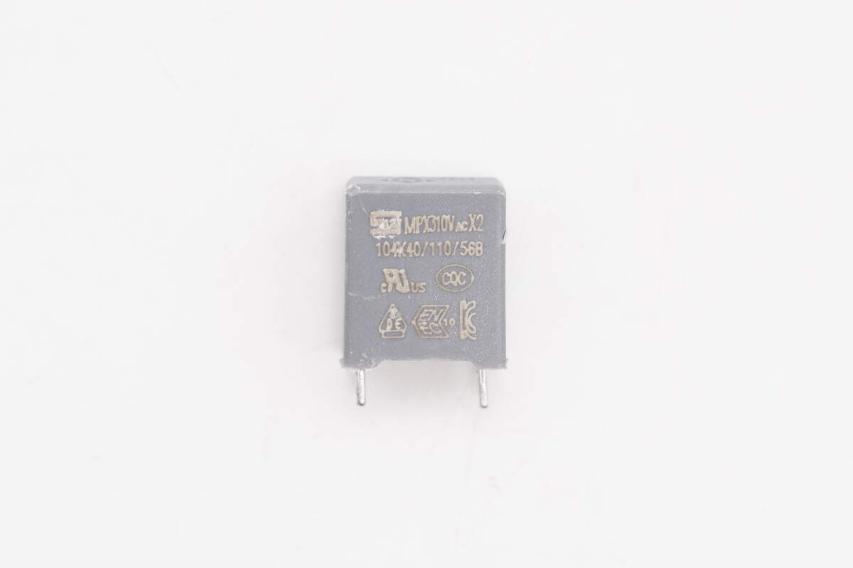
The safety X2 capacitor is from STE. 0.1μF.
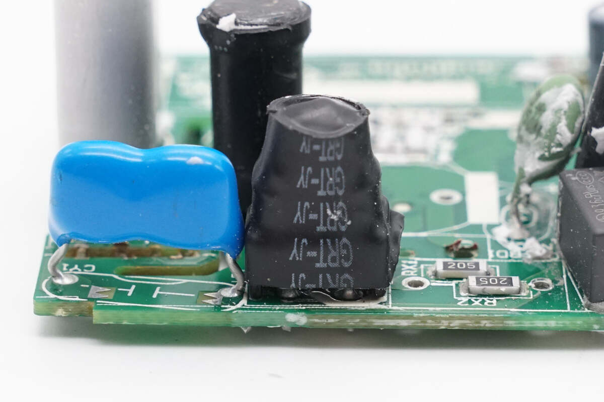
The common mode choke is insulated by heat-shrinkable tubing.
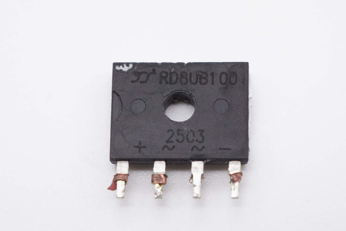
The bridge rectifier is from YJ and uses the D3K package. 8A 1000V. Model is RD8UB100.
The I-shaped inductor is insulated by heat-shrinkable tubing.
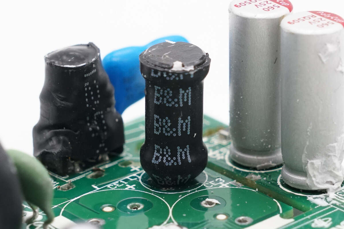
At the front end of the module, there is a capacitor that supplies power to the master control chip, and at the center, there are three electrolytic capacitors.
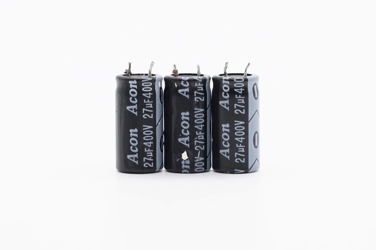
The three electrolytic capacitors are from Acon. 400V 27μF.
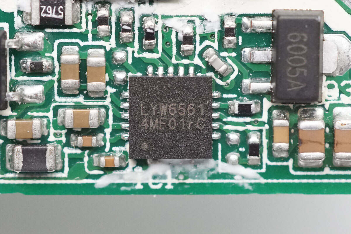
The master control chip is marked with LYW6561.
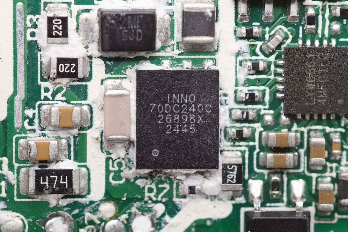
The MOSFET is from Innoscience. It is a 700V enhancement-mode GaN power transistor with an on-resistance of 240 mΩ. Designed to meet JEDEC standards for industrial applications, it features built-in ESD protection and comes in a DFN5×6 package. Model is INN700DC240C.
Here is the information about Innoscience INN700DC240C.
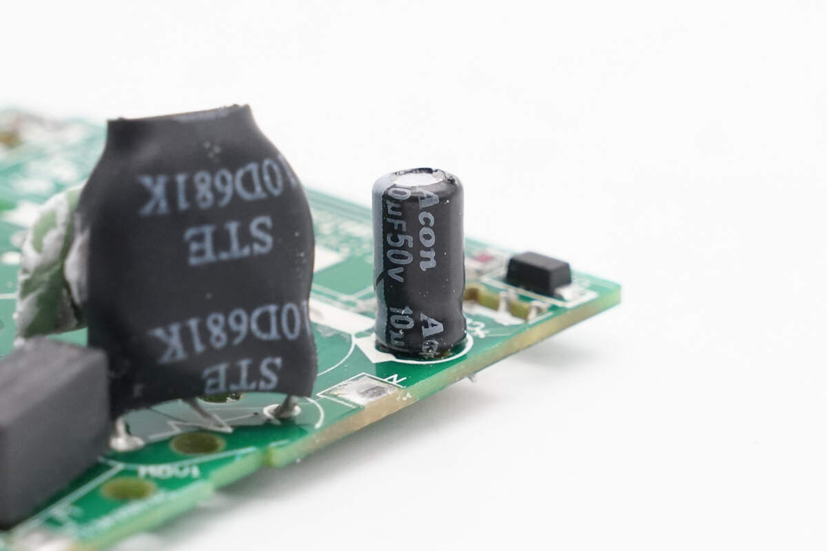
The capacitor that supplies power to the master control chip is also from Acon. 50V 10μF.
On the other side, a planar transformer module is soldered and enclosed in a plastic casing for insulation and protection.
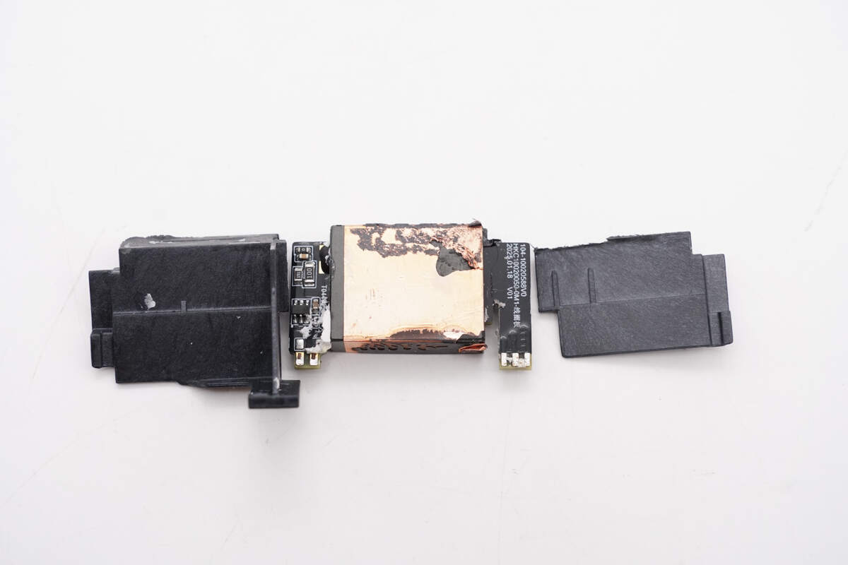
After removing the planar transformer module and taking off the plastic casing, the magnetic core is found to be wrapped with copper foil.
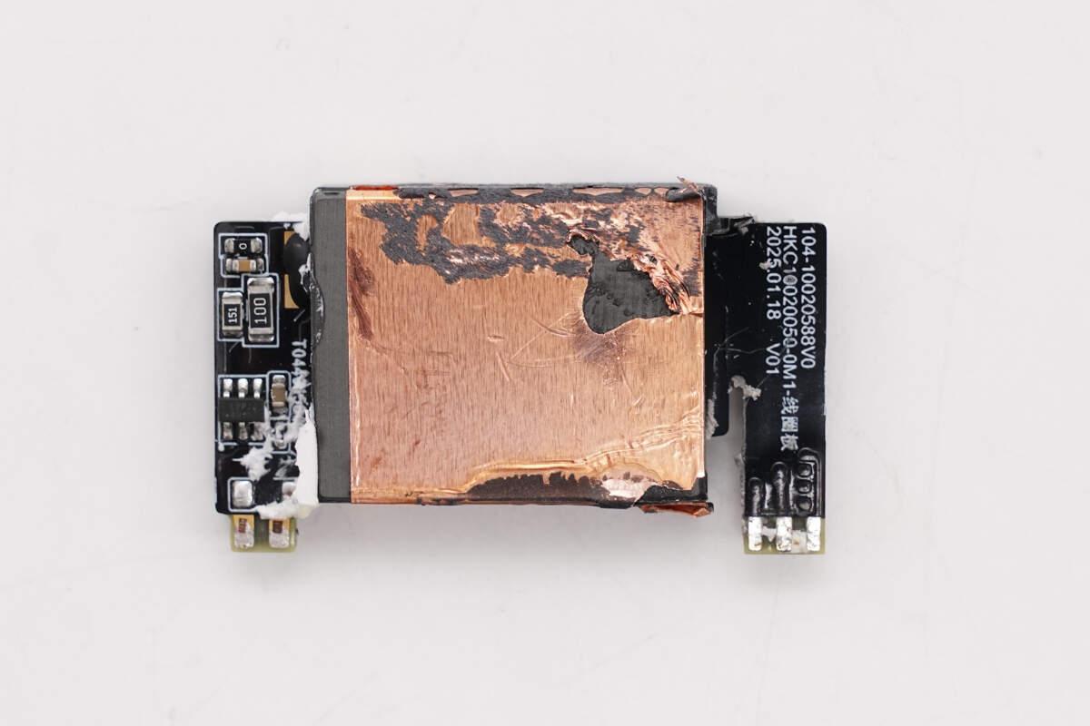
On the left side of the planar transformer module, there is a synchronous rectifier controller.
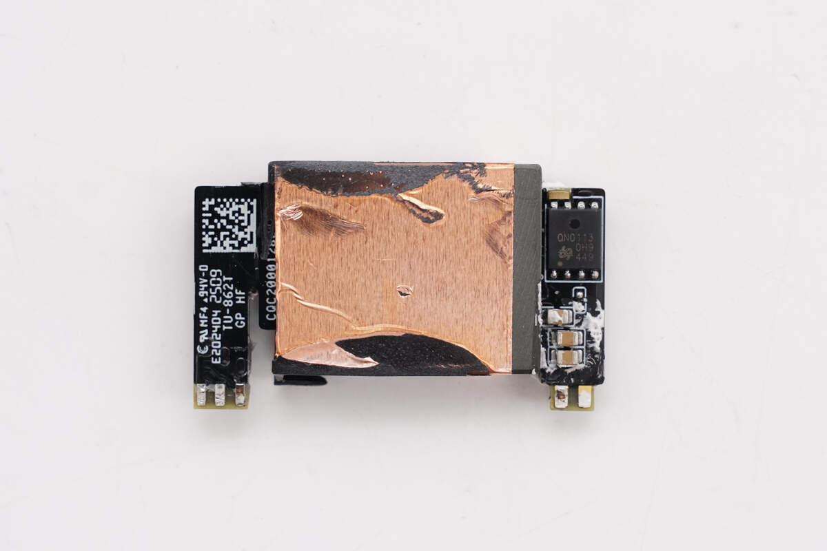
The synchronous rectifier corresponding to the synchronous rectifier controller is located on the back side.
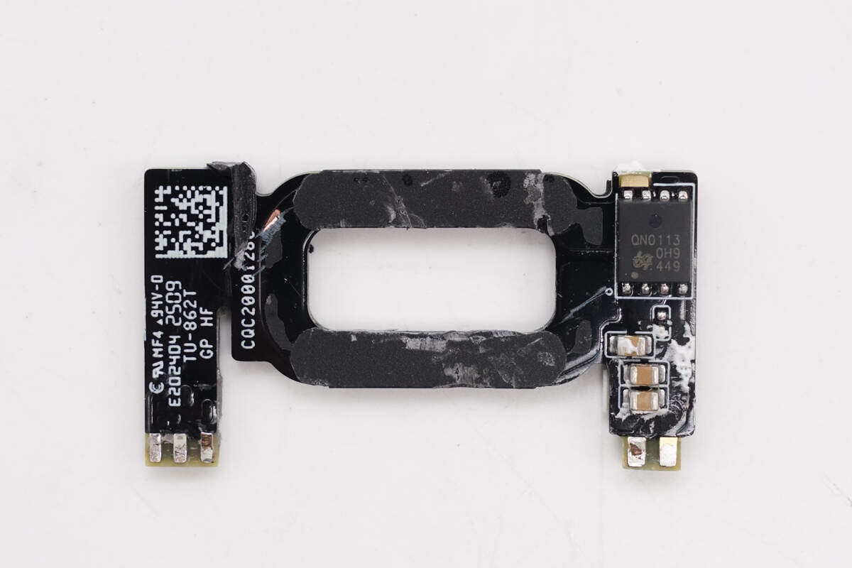
Breaking the magnetic core reveals an overview of the racetrack-shaped coil inside the planar transformer.
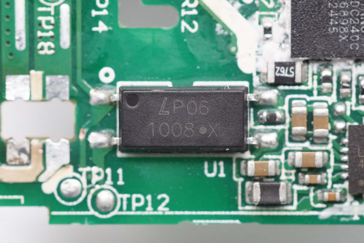
The 1008 optocoupler is used for output voltage feedback.
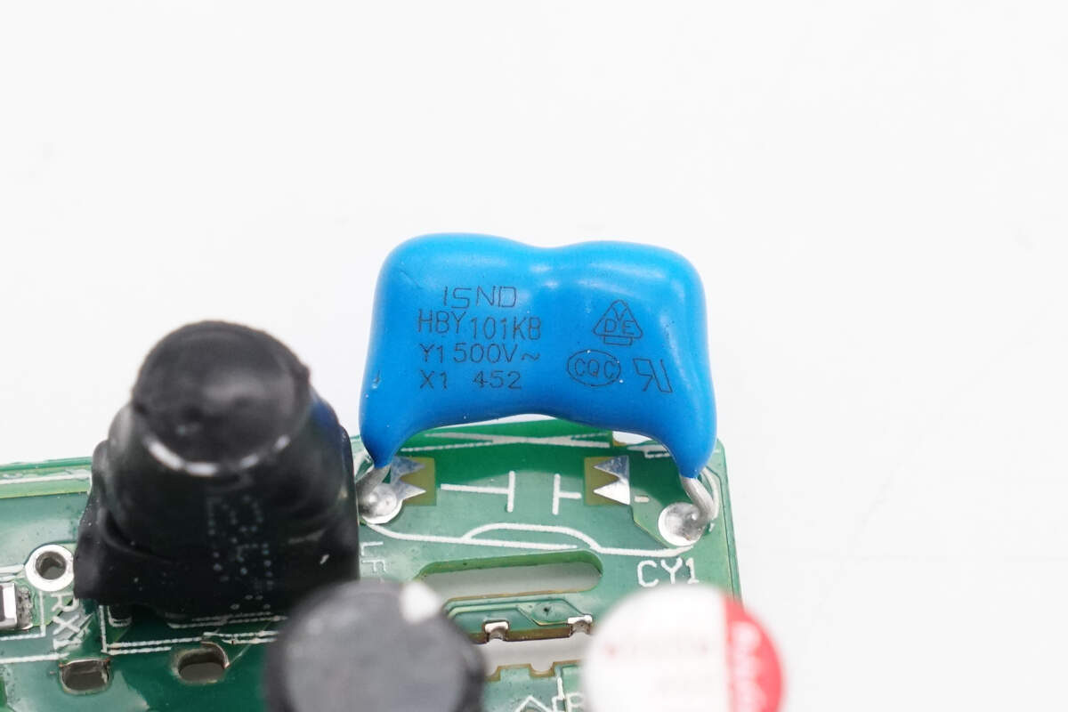
The Y capacitor is from ISND and features a double-insulation design in series.
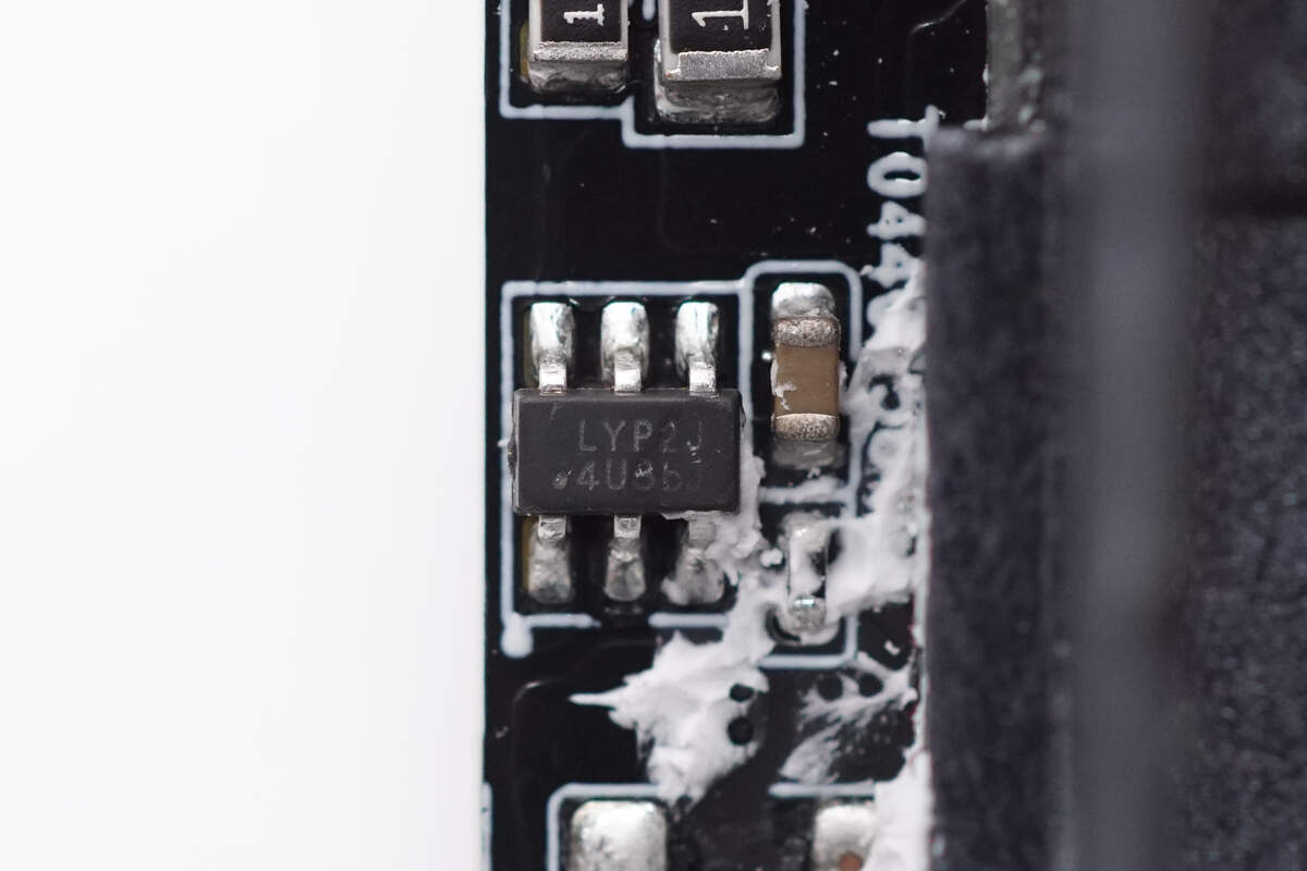
The synchronous rectifier controller is marked with LYP2J.
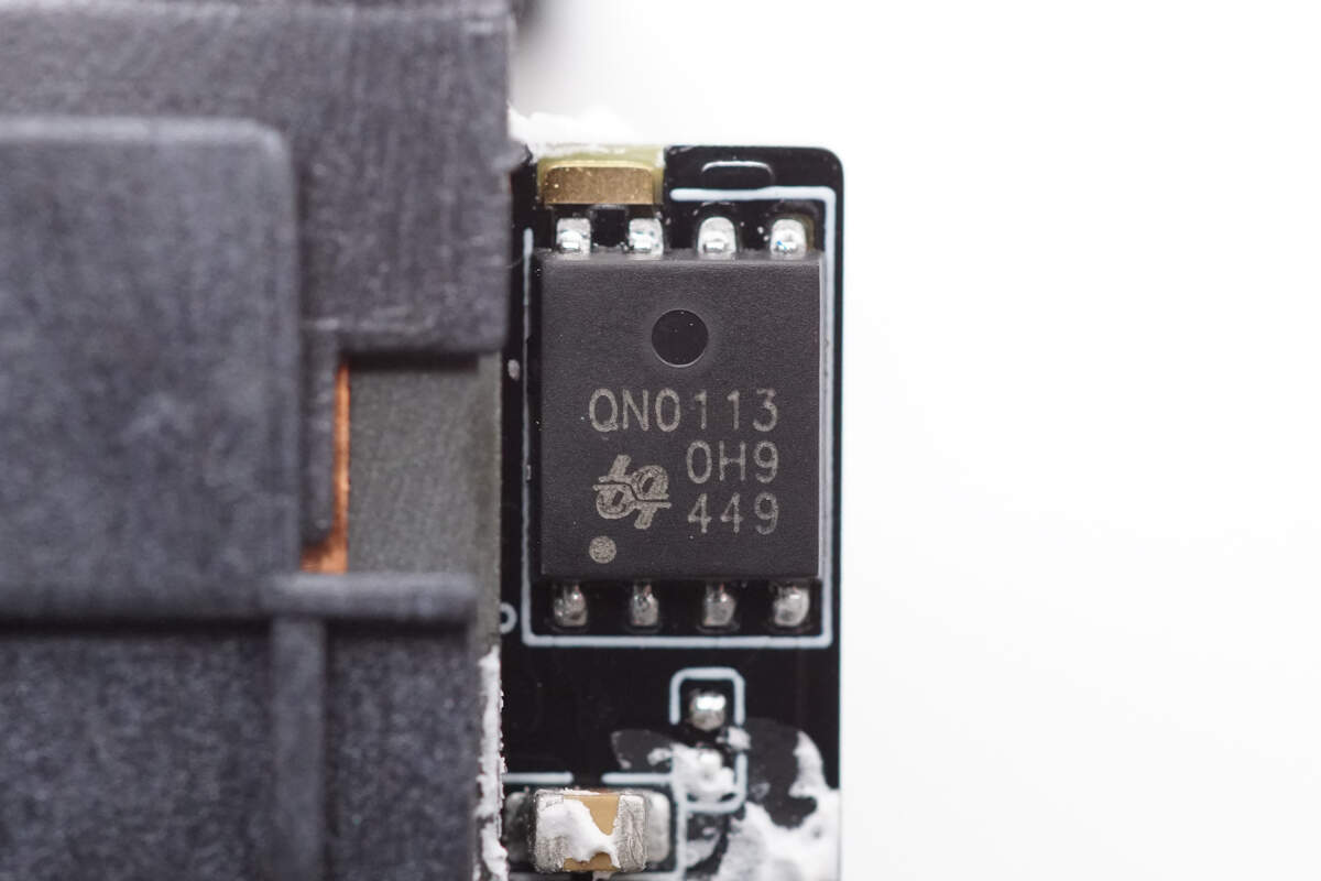
The synchronous rectifier is from uPI. It is an NMOS transistor with a voltage rating of 100V and an on-resistance of 6mΩ, housed in a PRPAK5×6 package. Model is QN0113M6N.
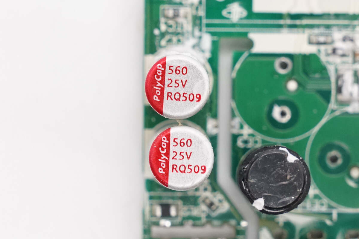
The two solid capacitors for output filtering are from PolyCap, both rated at 25V 560μF.
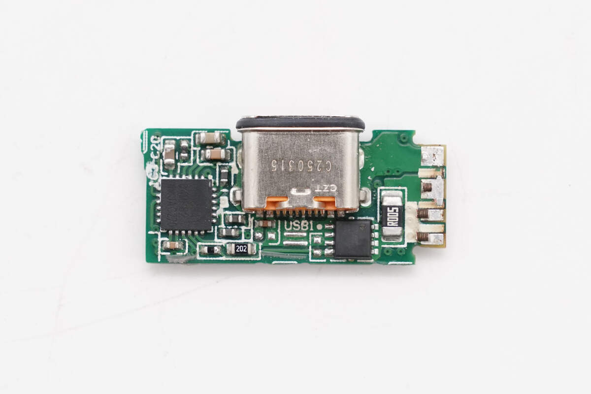
On the front side of the output PCB, there are a protocol chip, an output VBUS MOSFET, and a USB-C socket.
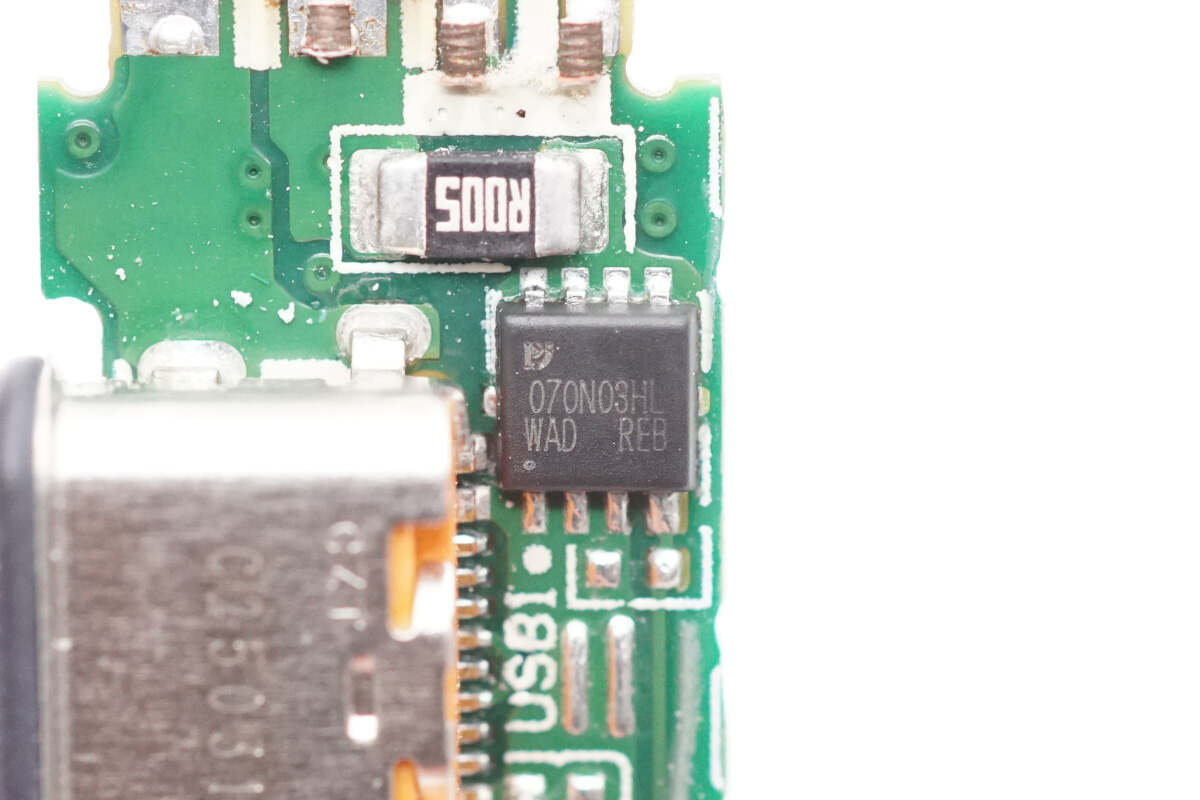
The output VBUS MOSFET marked with 070N03HL is from Pingwei and uses a DFN3×3 package.
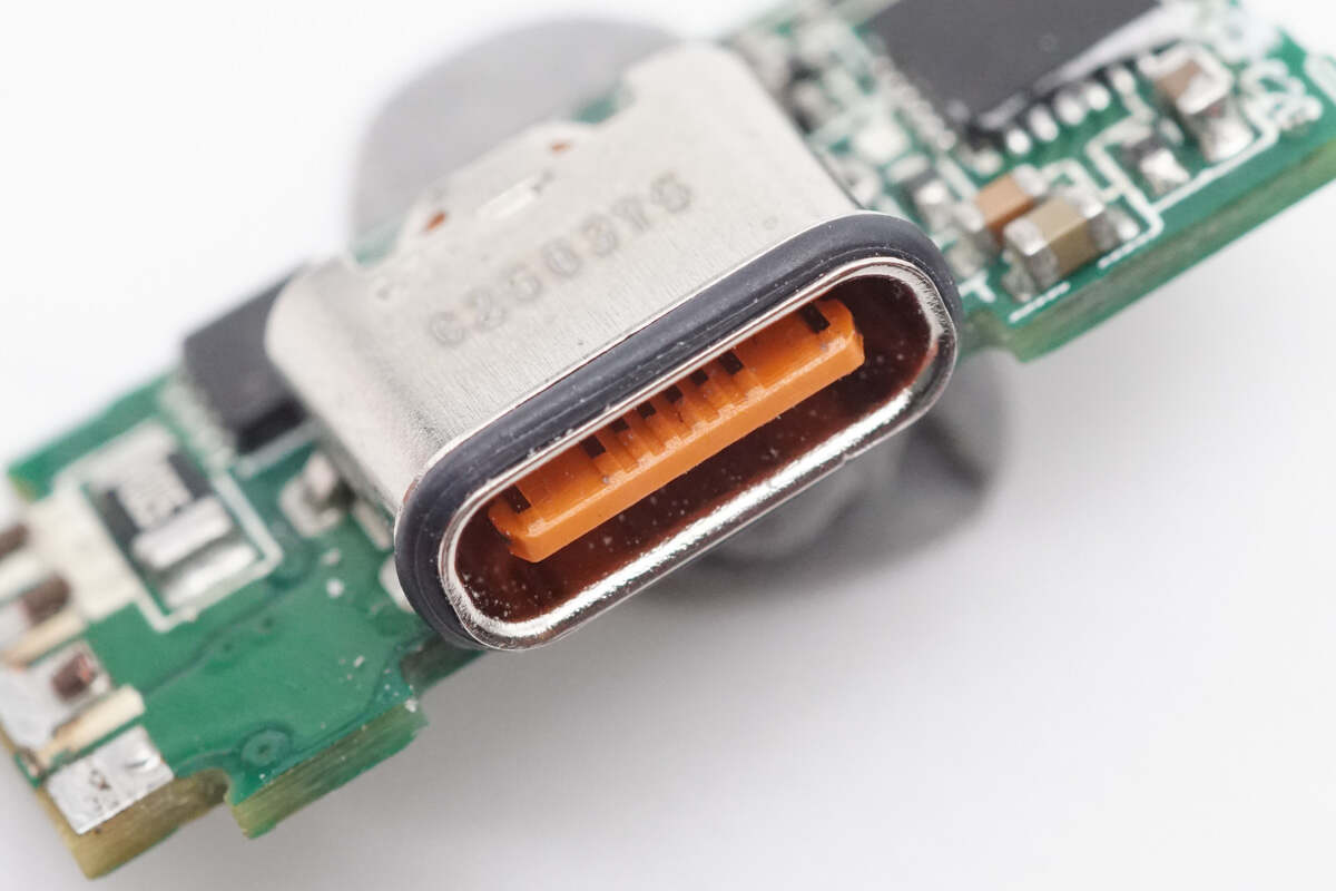
Close-up of the USB-C socket.

Well, those are all components of the Huawei 100W SuperCharge GaN Charger.
Summary of ChargerLAB
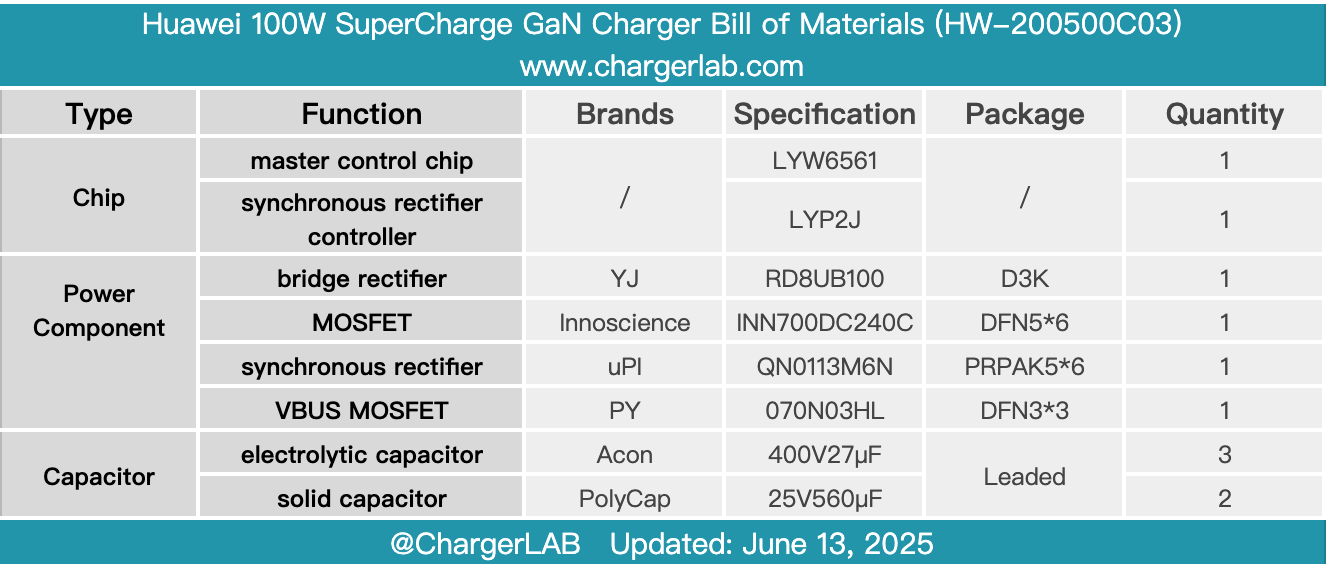
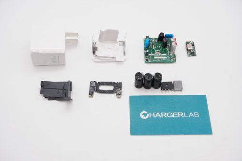
Here is the component list of the Huawei 100W SuperCharge GaN Charger for your convenience.
Its size is almost the same as the previously disassembled 66W model, but the maximum output power has been significantly increased. This not only ensures the compact and portable but also meets the needs of users with higher performance requirements. It supports UFCS, FCP, SCP, QC2.0, PD3.0, and PPS fast charging protocols, making it compatible not only with Huawei devices but also well-suited for Apple, Samsung, and other brand products.
After taking it apart, we found that it uses a GaN solution combined with a compact planar transformer module, further reducing the size of the PCBA. In addition, the component layout is compact, with added isolation plates, heat sinks, and more. The components are reinforced with potting compound, making the entire module more stable and reliable.
Thanks to the efficient power design, it supports intelligent temperature control as well as 12 protection functions, including short circuit, overcurrent, overvoltage, and undervoltage, ensuring fast charging that won’t damage the device and making charging safer.
Related Articles:
1. Teardown of Huawei Pura X Original 66W GaN Charger (HW-110600C05)
2. Teardown of Xiaomi 90W GaN Pudding Charger (MDY-18-EU)
3. Teardown of vivo 90W FlashCharge GaN Charger (V9082L0E1-CN)